JP3935847B2 - Programmable logic device including programmable interface core and central processing unit - Google Patents
Programmable logic device including programmable interface core and central processing unit Download PDFInfo
- Publication number
- JP3935847B2 JP3935847B2 JP2002591993A JP2002591993A JP3935847B2 JP 3935847 B2 JP3935847 B2 JP 3935847B2 JP 2002591993 A JP2002591993 A JP 2002591993A JP 2002591993 A JP2002591993 A JP 2002591993A JP 3935847 B2 JP3935847 B2 JP 3935847B2
- Authority
- JP
- Japan
- Prior art keywords
- data
- master
- slave
- address
- signal
- Prior art date
- Legal status (The legal status is an assumption and is not a legal conclusion. Google has not performed a legal analysis and makes no representation as to the accuracy of the status listed.)
- Expired - Lifetime
Links
Images


Classifications
-
- G—PHYSICS
- G06—COMPUTING; CALCULATING OR COUNTING
- G06F—ELECTRIC DIGITAL DATA PROCESSING
- G06F15/00—Digital computers in general; Data processing equipment in general
- G06F15/76—Architectures of general purpose stored program computers
- G06F15/78—Architectures of general purpose stored program computers comprising a single central processing unit
- G06F15/7867—Architectures of general purpose stored program computers comprising a single central processing unit with reconfigurable architecture
Landscapes
- Engineering & Computer Science (AREA)
- Computer Hardware Design (AREA)
- Theoretical Computer Science (AREA)
- Physics & Mathematics (AREA)
- General Engineering & Computer Science (AREA)
- General Physics & Mathematics (AREA)
- Logic Circuits (AREA)
- Bus Control (AREA)
- Microcomputers (AREA)
- Stored Programmes (AREA)
Description
発明の分野
この発明は、プログラマブルロジックデバイスに関し、具体的には、インターフェイスコアおよび中央処理装置を含むプログラマブルロジックデバイスに関する。
The present invention relates to programmable logic devices, and in particular to programmable logic devices that include an interface core and a central processing unit.
関連技術の説明
マイクロプロセッサは、コンピュータを制御する周知の集積回路である。マイクロプロセッサがコンピュータを制御する様態によって、コンピュータの速度およびパワーが決定される。コンピュータを制御するために、マイクロプロセッサは、無数の命令を処理し、その各々が、マイクロプロセッサに対してある特定の動作を実行するように伝える。典型的なマイクロプロセッサは、所望の演算および論理機能を実行する中央処理装置(CPU)およびCPUが入力を受取ってこれらの機能を実行し、および/または、その結果をコンピュータの構成要素の残りの部分と通信することを可能にする入力/出力ユニットを含む。
2. Description of Related Art A microprocessor is a well-known integrated circuit that controls a computer. The manner in which the microprocessor controls the computer determines the speed and power of the computer. To control the computer, the microprocessor processes a myriad of instructions, each telling the microprocessor to perform a certain operation. A typical microprocessor is a central processing unit (CPU) that performs the desired arithmetic and logic functions and the CPU receives these inputs to perform these functions and / or passes the results to the rest of the computer components. Includes an input / output unit that allows communication with the part.
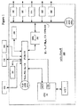
図1は、CPU101および2つの拡張バス102および103を含む公知のマイクロプロセッサ100を例示する。拡張バスによって、CPU101が他のデバイスと通信することが可能となり、マイクロプロセッサの動作が拡張される。プロセッサローカルバス(PLB)とも称される拡張バス102は、CPU101を高速デバイス104に接続する。これらの高速デバイス104は、メモリおよび高性能の周辺装置を含み得る。PLB102を制御してそれ自体の転送を扱うデバイスが、「マスタ」と呼ばれ、マスタからコマンドを受取ってデータを送るデバイスが、「スレーブ」と呼ばれる。
FIG. 1 illustrates a
オンチップ周辺バス(OPB)とも称される拡張バス103が、低速デバイス105へのアクセスをCPU101に提供する。これらの低速デバイス105は、UARTおよびイーサネット(R)接続を含み得る。なお、低速デバイス105は、高速デバイス104のように、マスタとスレーブとの両方を含み得る。しかしながら、これらの低速デバイス105がCPU101の性能に影響を及ぼすことを防ぐために、OPB103は、CPU101に直接接続されない。代わりに、OPB103は、OPBブリッジ106を介してPLB102に結合される。低速デバイスにメインバス上の貴重な帯域幅を消費させないように、大部分のシステムで、バスのセグメンテーションが行なわれることが検討されることが注目されるべきである。しかしながら、メインバスにほとんど影響を及ぼさずに、より高速の周辺装置の有利な動作を可能にする、メインバスと並列なバスとして、セグメンテーション部を扱うことが、多くの場合に有利である。OPBブリッジ106は、データを1つのバスから別のものへと移動させるように設計されるシステムビルディングブロックである。OPBブリッジ106は、自動的にデータフォーマットおよびプロトコルを変換し得、OPB103とPLB102との間の情報転送を容易にする。
An expansion bus 103, also referred to as an on-chip peripheral bus (OPB), provides the
特定用途向け集積回路(ASIC)も、集積回路技術において周知である。ASICは、予め定められたアプリケーション用に設計されるチップである。ASICを構築するために、複数の基本的な回路セルが相互接続される。通例、これらの回路セルは、ASICのメーカによって提供されるライブラリ内で見つけられる。現在、いくつかのメーカは、ASIC上での集積のためのマイクロプロセッサセルを提供している。これらの種類のマイクロプロセッサは、「組込用(embedded)」マイクロプロセッサと呼ばれる。 Application specific integrated circuits (ASICs) are also well known in integrated circuit technology. An ASIC is a chip designed for a predetermined application. In order to build an ASIC, a plurality of basic circuit cells are interconnected. Typically, these circuit cells are found in a library provided by the ASIC manufacturer. Currently, some manufacturers offer microprocessor cells for integration on ASICs. These types of microprocessors are referred to as “embedded” microprocessors.
プログラマブルロジックデバイス(PLD)も、集積回路技術において周知である。PLDは、論理設計を実現するフィールドでユーザによってプログラムされ得る。1つの種類のPLDは、書替え可能ゲートアレイ(FPGA)である。通例のアーキテクチャでは、FPGAは、プログラマブル入力/出力ブロック(IOB)によって囲まれるコンフィギャラブルロジックブロック(CLB)のアレイを含む。IOBは、パッケージピンとCLBとの間でインターフェイスを提供し、CLBは、FPGA上でロジックを構成するための機能的要素を提供する。CLBおよびIOBは、プログラマブルルーティングリソースの階層によって相互接続される。これらのCLB、IOB、およびプログラマブルルーティングリソースは、コンフィギュレーションビットストリームをFPGAにロードすることによって、カスタマイズされる。このコンフィギュレーションビットストリームは、ソフトウェアツールを用いて生成される。 Programmable logic devices (PLDs) are also well known in integrated circuit technology. The PLD can be programmed by the user in the field that implements the logic design. One type of PLD is a rewritable gate array (FPGA). In a typical architecture, an FPGA includes an array of configurable logic blocks (CLB) surrounded by programmable input / output blocks (IOBs). The IOB provides an interface between the package pins and the CLB, and the CLB provides functional elements for configuring logic on the FPGA. CLBs and IOBs are interconnected by a hierarchy of programmable routing resources. These CLB, IOB, and programmable routing resources are customized by loading the configuration bitstream into the FPGA. This configuration bitstream is generated using a software tool.
図2は、ザイリンクス社(Xilinx, Inc.)が販売するバーテックス(Virtex)(商標)FPGA内のCLB200を示す簡素化されたブロック図を例示する。CLB200は、2つの「スライス」201Aおよび201Bを含む。各スライス201は、プログラマブルインターコネクトから第1の複数の入力信号G1−G4を受けるための第1のLUT202と、同様にプログラマブルインターコネクトから第2の複数の入力信号F1−F4を受けるための第2のLUT203とを含む。各スライス201は、LUT202からの出力信号Yを(そのD端子上で)受け、さらには信号YQを(そのQ端子上で)出力するためのフリップフロップ204をさらに含む。同様の様態で、各スライス201は、LUT203からの出力信号Xを(そのD端子上で)受け、さらには信号XQを(そのQ端子上で)出力するためのフリップフロップ205をさらに含む。バーテックス(商標)FPGAについてのこれ以外の詳細は、ザイリンクス社によって出版される「プログラマブルロジックデータブック2000」(“The Programmable Logic Data Book 2000”)の第3−7頁から第3−17頁、および第3−76頁から第3−87頁上に開示される。 FIG. 2 illustrates a simplified block diagram illustrating CLB 200 in a Virtex ™ FPGA sold by Xilinx, Inc. The CLB 200 includes two “slices” 201A and 201B. Each slice 201 has a first LUT 202 for receiving a first plurality of input signals G1-G4 from the programmable interconnect and a second for receiving a second plurality of input signals F1-F4 from the programmable interconnect as well. LUT203. Each slice 201 further includes a flip-flop 204 for receiving the output signal Y from the LUT 202 (on its D terminal) and outputting the signal YQ (on its Q terminal). In a similar manner, each slice 201 further includes a flip-flop 205 for receiving the output signal X from the LUT 203 (on its D terminal) and further outputting the signal XQ (on its Q terminal). Additional details on the Vertex ™ FPGA are described on pages 3-7 to 3-17 of “The Programmable Logic Data Book 2000” published by Xilinx, and It is disclosed on pages 3-76 to 3-87.
バーテックスFPGAのようないくつかのFPGAは、「コア」と呼ばれる予め設計された機能を備えたブロックを組込むようにプログラムされ得る。一実施例では、コアは、1つ以上の機能を実行するようにFPGAをプログラムする予め定められたコンフィギュレーションビットセットを含み得る。別の実施例では、コアは、設計の接続性および論理を示す回路図(schematics)またはソースコードを含み得る。典型的なコアは、デジタル信号処理(DSP)機能、メモリ、記憶素子、および数学的機能を提供し得るが、これらに限定されているわけではない。コアには、特定のFPGAのための、最適に構成されたレイアウトが提供され得る。コアはさらに、パラメータ表示可能であり得、つまり、ユーザがパラメータを入力して特定のコア機能を活性化または変更することを可能にする。 Some FPGAs, such as vertex FPGAs, can be programmed to incorporate a block with a pre-designed function called a “core”. In one embodiment, the core may include a predetermined set of configuration bits that program the FPGA to perform one or more functions. In another embodiment, the core may include schematics or source code indicating design connectivity and logic. A typical core may provide, but is not limited to, digital signal processing (DSP) functions, memory, storage elements, and mathematical functions. The core can be provided with an optimally configured layout for a particular FPGA. The core may further be parameterizable, i.e., allow a user to enter parameters to activate or change a particular core function.
図3は、FPGA内で1つ以上のコアを用いるための1つのIPプロセスレイアウト300を例示する。ここで、IPとは、FPGAのための論理設計等の一般的な知的財産を指す。この発明の譲受人または他によって開発された、ユーザおよびコアによって提供される両方の論理設計が、IPとみなされる。レイアウト300では、システムレベルツール301によって活性化されるコアジェネレータ304が、サードパーティが提供する1つ以上のプラグインコア302を受取り得る。代替的には、コアジェネレータ304は、ライブラリセット303内で提供されるコアを用い得、これらのライブラリ303は、コアジェネレータ304の一部を形成する。一旦コアが選択されると、それは、FPGAソフトウェアツール306に提供され得る。例示的なFPGAソフトウェアは、アライアンス(Alliance)(商標)、ファンデーション(Foundation)(商標)、またはファンデーションISE(商標)ソフトウェアを含み得、すべてが、この発明の譲受人によってライセンス供与されている。このソフトウェアは、ユーザが提供するトップレベル設計305を受取ることもできる。このトップレベル設計は、コアに加えてFPGA上で実現される論理設計を示す。一実施例では、FPGAソフトウェアツール306は、VHDL、Ve
rilog、または標準の概略的な形で、トップレベル設計305を受取り得る。FPGAソフトウェアツール306は、FPGA307をプログラムするコンフィギュレーションビットストリームを生成して、コアおよびトップレベル設計によって指定される機能を提供する。
FIG. 3 illustrates one
The top-
技術の向上が実現されるにつれて、FPGAは、以前はASIC専用であったアプリケーションへとますます移行しつつある。しかしながら、物理的なリソースは、ASIC上よりもFPGA上においてより制約される。したがって、FPGA上でマイクロプロセッサ構成要素を提供することは、特別な配慮を必要とする重要な作業となる。 As technology improvements are realized, FPGAs are increasingly migrating to applications that were previously dedicated to ASICs. However, physical resources are more constrained on the FPGA than on the ASIC. Thus, providing microprocessor components on an FPGA is an important task that requires special consideration.
発明の概要
この発明に従うと、プログラマブルロジックデバイス(PLD)は、中央処理装置(CPU)およびCPUに結合されるプログラマブルインターフェイスを含み、プログラマブルインターフェイスは、ユーザによって指定されるコアにより作成される。通例、PLDは、複数のデバイスをさらに含み、各デバイスは、プログラマブルインターフェイスを介してCPUに情報を提供するか、プログラマブルインターフェイスを介してCPUから情報を受取るか、またはプログラマブルインターフェイスを介して別のデバイスと通信するかのいずれかである。
SUMMARY OF THE INVENTION According to the present invention, a programmable logic device (PLD) includes a central processing unit (CPU) and a programmable interface coupled to the CPU, the programmable interface being created by a core specified by the user. Typically, the PLD further includes a plurality of devices, each device providing information to the CPU via the programmable interface, receiving information from the CPU via the programmable interface, or another device via the programmable interface. Either to communicate with.
一実施例では、プログラマブルインターフェイスは、複数のデバイスを結合するためのクロスポイントスイッチを含む。クロスポイントスイッチは、アドレス/制御経路とデータ経路との両方を含む。アドレス/制御経路は、PLD上の第1のプログラマブルリソースセットから形成され得、データ経路は、PLD上の第2のプログラマブルリソースセットから形成され得る。第1および第2のプログラマブルリソースセットは、別々であり得るか、またはPLD上でオーバーラップし得る。 In one embodiment, the programmable interface includes a crosspoint switch for coupling a plurality of devices. The crosspoint switch includes both an address / control path and a data path. The address / control path may be formed from a first programmable resource set on the PLD and the data path may be formed from a second programmable resource set on the PLD. The first and second programmable resource sets may be separate or may overlap on the PLD.
一実施例では、PLDは、プログラマブルインターフェイスに結合されるオンチップ周辺バス(OPB)をさらに含む。ブリッジモジュールが、OPBをプログラマブルインターフェイスに結合する。マスタとスレーブとの両方を含む、PLD上の第1のデバイスグループが、OPBに結合され得る。したがって、この第1のマスタおよびスレーブグループは、ブリッジモジュールを用いてプログラマブルインターフェイスと通信し得る。第1のマスタおよびスレーブグループは、低速デバイスとして通例特徴づけられる周辺デバイスを含み得る。一実施例では、これらのマスタおよびスレーブのうちの少なくとも1つが、コアを用いるPLD上で作成される。別の実施例では、これらのマスタおよびスレーブのうちの少なくとも1つが、チップ外に置かれる。さらに別の実施例では、コアを用いて、マスタ機能とスレーブ機能との両方を有するデバイス(第1のグループのうちの1つ)が作成され得る。第1のデバイスグループは、PLD上またはチップ外に存在し得る。 In one embodiment, the PLD further includes an on-chip peripheral bus (OPB) coupled to the programmable interface. A bridge module couples the OPB to the programmable interface. A first device group on the PLD, including both masters and slaves, can be coupled to the OPB. Thus, this first master and slave group can communicate with the programmable interface using the bridge module. The first master and slave group may include peripheral devices that are typically characterized as low speed devices. In one embodiment, at least one of these masters and slaves is created on a PLD that uses the core. In another embodiment, at least one of these masters and slaves is placed off-chip. In yet another example, the core may be used to create a device (one of the first group) that has both a master function and a slave function. The first device group may exist on the PLD or off-chip.
同様にマスタおよびスレーブを含む、PLD上の第2のデバイスグループは、プログラマブルインターフェイスに結合され得る。第2のデバイスグループは、メモリデバイスまたはダブルデータレートデバイス等の高速デバイスを含み得る。第2のデバイスグループは、PLD上またはチップ外に存在し得る。一実施例では、第2のデバイスグループ内のマスタのうちの1つは、プログラマブルインターフェイスおよびOPBに結合される高速バスインターフェイスを含み、高速バスインターフェイスは、チップ外のデバイスに通信を提供する。この発明のPLDは、他の構成要素を含むシステムに容易に組込まれ得、プログラマブルインターフェイスおよび高速バスインターフェイスは、有利なことには、これらの構成要素に対して、CPU関連の機能への効率的なアクセスを提供する。 A second group of devices on the PLD, including masters and slaves as well, may be coupled to the programmable interface. The second device group may include high speed devices such as memory devices or double data rate devices. The second device group may exist on the PLD or off-chip. In one embodiment, one of the masters in the second device group includes a high speed bus interface coupled to the programmable interface and the OPB, the high speed bus interface providing communication to off-chip devices. The PLD of the present invention can be easily incorporated into a system that includes other components, and the programmable and high-speed bus interfaces advantageously provide an efficient for CPU-related functions for these components. Provide secure access.
この発明の一実施例では、プログラマブルインターフェイスは、クロスポイントスイッチを含む。アドレス/制御論理では、クロスポイントスイッチは、アドレスをマスタから受取るための複数のアドレスデコーダと、デコードされたアドレスをアドレスデコーダから受取り、さらにはマスタとスレーブとの間でトランザクションをアービトレートするための複数のアクセスアービタとを含み得る。クロスポイントスイッチは、アドレスデコーダとアクセスアービタとの間で、十分な、またはそれ未満の接続性を提供し得る。 In one embodiment of the present invention, the programmable interface includes a crosspoint switch. In address / control logic, the crosspoint switch has a plurality of address decoders for receiving addresses from the master, a plurality of address decoders for receiving decoded addresses from the address decoder, and for arbitrating transactions between the master and slaves. Access arbiters. The crosspoint switch may provide sufficient or less connectivity between the address decoder and the access arbiter.
データ論理では、クロスポイントスイッチは、マスタから書込データを受取るための複数の書込マルチプレクサを含み得、各書込マルチプレクサは、書込データを1つのスレーブに対して選択的に提供し、クロスポイントスイッチは、スレーブから読出データを受取るための複数の読出マルチプレクサを含み得、各読出マルチプレクサは、読出データを1つのマスタに選択的に提供する。書込マルチプレクサおよび読出マルチプレクサは、複数のアクセスアービタによって制御され得る。クロスポイントスイッチは、各書込マルチプレクサと複数のマスタデバイスとの間で、十分な、またはそれ未満の接続性を提供し得る。クロスポイントスイッチはまた、各読出マルチプレクサと複数のスレーブデバイスとの間で、十分な、またはそれ未満の接続性を提供し得る。一実施例では、アドレス/制御および/またはデータ論理は、マスタとスレーブとの間のトランザクションをパイプライン化するためのレジスタをさらに含む。 In data logic, the crosspoint switch may include multiple write multiplexers for receiving write data from the master, each write multiplexer selectively providing write data to one slave, The point switch may include a plurality of read multiplexers for receiving read data from slaves, each read multiplexer selectively providing read data to one master. The write multiplexer and read multiplexer can be controlled by multiple access arbiters. A crosspoint switch may provide sufficient or less connectivity between each write multiplexer and multiple master devices. The crosspoint switch may also provide sufficient or less connectivity between each read multiplexer and multiple slave devices. In one embodiment, the address / control and / or data logic further includes a register for pipelining transactions between the master and the slave.
この発明の別の実施例に従うと、組込用中央処理装置(CPU)を有する書替え可能ゲートアレイ(FPGA)は、コアによって作られるハイブリッドスイッチを含み、ハイブリッドスイッチは、FPGA上で実現されるユーザ論理とCPUとの間で通信を提供する。この実施例では、CPUは、マスタデバイスを含み、論理は、複数のスレーブデバイスおよび複数のマスタデバイスを含む。このハイブリッドスイッチは、クロスポイントおよび共有バス構成の両方を含んで、マスタデバイスとスレーブデバイスとの間に経路を提供する。 According to another embodiment of the present invention, a rewritable gate array (FPGA) having an embedded central processing unit (CPU) includes a hybrid switch made by a core, the hybrid switch being a user implemented on the FPGA. Provides communication between logic and CPU. In this embodiment, the CPU includes a master device and the logic includes a plurality of slave devices and a plurality of master devices. This hybrid switch provides a path between the master and slave devices, including both crosspoint and shared bus configurations.
具体的には、ハイブリッドスイッチは、マスタからアドレスを受取るための複数のアドレスデコーダと、デコードされたアドレスをアドレスデコーダから受取り、さらにはマスタとスレーブとの間でトランザクションをアービトレートするための複数のアクセスアービタとを含み得る。少なくとも1つのアクセスアービタが、1つよりも多くのスレーブに対してアービトレーションを提供し、少なくとも1つのアクセスアービタが、1つのスレーブに対してのみアービトレーションを提供する。クロスポイントスイッチはまた、書込データをマスタから受取り、さらには書込データをスレーブに提供するための複数の書込マルチプレクサを含み得る。一実施例では、少なくとも1つの書込マルチプレクサが、その書込データを1つよりも多くのスレーブに提供し、少なくとも1つの書込マルチプレクサが、その書込データを1つのスレーブに対してのみ提供する。クロスポイントスイッチは、読出データをスレーブから受取り、さらには読出データをマスタに選択的に提供するための複数の読出マルチプレクサも含み得る。一実施例では、少なくとも1つの読出マルチプレクサが、その読出データを1つよりも多くのマスタに提供し、少なくとも1つの読出マルチプレクサが、その読出データを1つのマスタに対してのみ提供する。書込マルチプレクサおよび読出マルチプレクサは、複数のアクセスアービタによって制御され得る。ハイブリッドスイッチは、この発明のクロスポイントスイッチのように、マスタとスレーブとの間のトランザクションのためのパイプライン方式を含み得る。 Specifically, the hybrid switch has a plurality of address decoders for receiving addresses from the master, a plurality of accesses for receiving decoded addresses from the address decoder, and further arbitrating transactions between the master and slaves. And an arbiter. At least one access arbiter provides arbitration for more than one slave, and at least one access arbiter provides arbitration for only one slave. The crosspoint switch may also include a plurality of write multiplexers for receiving write data from the master and further providing write data to the slave. In one embodiment, at least one write multiplexer provides the write data to more than one slave, and at least one write multiplexer provides the write data to only one slave. To do. The crosspoint switch may also include a plurality of read multiplexers for receiving read data from the slave and further selectively providing read data to the master. In one embodiment, at least one read multiplexer provides the read data to more than one master, and at least one read multiplexer provides the read data to only one master. The write multiplexer and read multiplexer can be controlled by multiple access arbiters. The hybrid switch may include a pipeline scheme for transactions between the master and slave, like the crosspoint switch of the present invention.
この発明の一実施例に従うと、書替え可能ゲートアレイ(FPGA)は、複数のマスタデバイスを含み、組込用マイクロプロセッサは、少なくとも1つのこのようなマスタデバイスであり、書替え可能ゲートアレイ(FPGA)はさらに、複数のスレーブデバイス、および複数のマスタデバイスと複数のスレーブデバイスとの間で接続性を選択的に提供す
るための手段を含む。接続性を選択的に提供するための手段は、コアによって生成され得る。
According to one embodiment of the present invention, a rewritable gate array (FPGA) includes a plurality of master devices, and the embedded microprocessor is at least one such master device, and the rewritable gate array (FPGA) Further includes a plurality of slave devices and means for selectively providing connectivity between the plurality of master devices and the plurality of slave devices. Means for selectively providing connectivity may be generated by the core.
アドレス/制御論理では、十分な接続性を選択的に提供するための手段は、マスタデバイスからのアドレスをデコードするための手段と、デコードされたアドレスに基づいて、複数のマスタデバイスと複数のスレーブデバイスとの間でトランザクションをアービトレートするための手段とを含み得る。一実施例では、接続性を選択的に提供するための手段は、デコードするための手段とアービトレートするための手段との間で、十分な接続性を提供し、他の実施例では、接続性を選択的に提供するための手段は、デコードするための手段とアービトレートするための手段との間で、十分には満たない接続性を提供する。 In the address / control logic, the means for selectively providing sufficient connectivity includes means for decoding an address from the master device, and a plurality of master devices and a plurality of slaves based on the decoded address. Means for arbitrating transactions with the device. In one embodiment, the means for selectively providing connectivity provides sufficient connectivity between the means for decoding and the means for arbitrating, and in other embodiments, the connectivity The means for selectively providing provides a less than sufficient connectivity between the means for decoding and the means for arbitrating.
データ論理では、接続性を選択的に提供するための手段は、書込データを複数のマスタデバイスから受取り、さらには指定されるスレーブデバイスに書込データを選択的に提供するための手段と、読出データを複数のスレーブデバイスから受取り、さらには指定されるマスタデバイスに読出データを選択的に提供するための手段とを含み得る。一実施例では、書込データを受取るための手段と読出データを受取るための手段とは、アービトレートするための手段によって制御される。 In data logic, the means for selectively providing connectivity comprises means for receiving write data from a plurality of master devices and further selectively providing write data to a designated slave device; Means for receiving read data from a plurality of slave devices and further selectively providing read data to a designated master device. In one embodiment, the means for receiving write data and the means for receiving read data are controlled by means for arbitrating.
接続性を選択的に提供するための手段は、書込データを受取るための手段と複数のマスタデバイスとの間で、十分な、またはそれ未満の接続性を提供し得る。加えて、接続性を選択的に提供するための手段は、読出データを受取るための手段と複数のスレーブデバイスとの間で、十分な、またはそれ未満の接続性を提供し得る。 The means for selectively providing connectivity may provide sufficient or less connectivity between the means for receiving write data and the plurality of master devices. In addition, the means for selectively providing connectivity may provide sufficient or less connectivity between the means for receiving read data and the plurality of slave devices.
有利なことには、この発明は、公知のPLDソフトウェアツールに含まれ得る。一実施例では、システムレベルツールによって活性化されるコアジェネレータは、サードパーティによって提供される、この発明のプログラマブルインターフェイスコアを受取り得る。代替的には、コアジェネレータは、コアジェネレータの一部を形成するライブラリセット内で提供されるプログラマブルインターフェイスコアを用い得る。一旦プログラマブルインターフェイスコアが選択されると、それは、PLDソフトウェアツールに提供され得る。このソフトウェアは、ユーザが提供するトップレベル設計も受取り得る。このPLDソフトウェアツールは、PLDをプログラムするコンフィギュレーションビットストリームを生成して、プログラマブルインターフェイスコアおよびトップレベル設計が指定する機能を提供する。 Advantageously, the present invention can be included in known PLD software tools. In one embodiment, a core generator activated by a system level tool may receive the programmable interface core of the present invention provided by a third party. Alternatively, the core generator may use a programmable interface core provided in a library set that forms part of the core generator. Once the programmable interface core is selected, it can be provided to the PLD software tool. This software can also accept top-level designs provided by the user. The PLD software tool generates a configuration bitstream that programs the PLD and provides the functionality specified by the programmable interface core and the top-level design.
重要なことには、この発明のプログラマブルインターフェイスコアは、複数のコンプライアンスレベルを有し得る。たとえば、コアは、特定の機能だけがPLD上で提供されることを許容し得る。たとえば、一実施例では、プロセッサローカルバス(PLB)機能のサブセットが許容される。既存のIPまたはパラメータ表示されないIPを含む実施例等の他の実施例では、この発明は、サブセットを、そのIPによって必要とされる機能に(または、そのIPに基づいた、予め定められたコンプライアンスレベルに)調整し得る。 Importantly, the programmable interface core of the present invention may have multiple compliance levels. For example, the core may allow only certain functions to be provided on the PLD. For example, in one embodiment, a subset of processor local bus (PLB) functions are allowed. In other embodiments, such as those that include an existing IP or an IP that is not parameterized, the present invention may apply a subset to a function required by that IP (or a predetermined compliance based on that IP). Can be adjusted).
この発明に従うと、プログラマブルロジックデバイス(PLD)上の中央処理装置(CPU)とユーザによって実現されるPLD上の論理との間でインターフェイスを提供するための方法が提供される。この方法は、論理が提供する複数のマスタデバイスと論理が提供する複数のスレーブデバイスとの間で接続性を選択的に提供するステップを含み、CPUは、少なくとも1つのマスタデバイスを含む。アドレス/制御論理中に接続性を選択的に提供するステップは、アドレスデコーダを用いてマスタデバイスからのアドレスをデコードし、さらにはアクセスアービタおよびデコードされたアドレスを用いて複数のスレーブデバイスと複数のマスタデバイスとの間でトランザクションをアービトレートするステップを含む。一実施例では、接続性を選択的に提供するステップは、アドレスデコーダと
アクセスアービタとの間の十分な接続性を提供する。別の実施例では、接続性を選択的に提供するステップは、アドレスデコーダとアクセスアービタとの間の十分には満たない接続性を提供する。
In accordance with the present invention, a method is provided for providing an interface between a central processing unit (CPU) on a programmable logic device (PLD) and logic on a PLD implemented by a user. The method includes selectively providing connectivity between a plurality of master devices provided by the logic and a plurality of slave devices provided by the logic, and the CPU includes at least one master device. The step of selectively providing connectivity during the address / control logic includes decoding an address from the master device using an address decoder, and further using the access arbiter and the decoded address to Arbitrating transactions with the master device. In one embodiment, the step of selectively providing connectivity provides sufficient connectivity between the address decoder and the access arbiter. In another embodiment, the step of selectively providing connectivity provides less than sufficient connectivity between the address decoder and the access arbiter.
この発明の方法では、データ論理内で接続性を選択的に提供するステップは、複数のマスタデバイスから書込データを受取り、さらには第1のマルチプレクサセットを用いて書込データを指定されるスレーブデバイスに選択的に提供するステップと、複数のスレーブデバイスから読出データを受取り、さらには第2のマルチプレクサセットを用いて読出データを指定されるマスタデバイスに選択的に提供するステップとを含む。接続性を選択的に提供するステップは、第1のマルチプレクサセットと複数のマスタデバイスとの間で、十分な、またはそれ未満の接続性を提供し得る。接続性を選択的に提供するステップは、第2のマルチプレクサセットと複数のスレーブデバイスとの間で、十分な、またはそれ未満の接続性も提供し得る。 In the method of the present invention, the step of selectively providing connectivity within the data logic receives write data from a plurality of master devices, and further slaves that are designated with the first multiplexer set. Selectively providing to the device; receiving read data from the plurality of slave devices; and further using the second multiplexer set to selectively provide the read data to the designated master device. The step of selectively providing connectivity may provide sufficient or less connectivity between the first multiplexer set and the plurality of master devices. The step of selectively providing connectivity may also provide sufficient or less connectivity between the second set of multiplexers and the plurality of slave devices.
この発明の方法では、接続性を選択的に提供するステップは、複数のマスタデバイスと複数のスレーブデバイスとの間でトランザクションをパイプライン化するステップを含む。有利なことには、このパイプライン化は、アドレス/制御論理およびデータ論理内で提供され得、したがって、両方において性能が向上する。 In the method of the invention, selectively providing connectivity includes pipeline transactions between a plurality of master devices and a plurality of slave devices. Advantageously, this pipelining can be provided within address / control logic and data logic, thus improving performance in both.
この発明に従うと、プログラマブルロジックデバイス(PLD)上の中央処理装置(CPU)とユーザによって実現されるPLD上の論理との間のインターフェイスを提供するための方法が与えられる。この方法は、ライブラリからコアを選択するステップを含み、コアは、論理が提供する複数のマスタデバイスと論理が提供する複数のスレーブデバイスとの間の接続性を選択的に提供し、CPUは、少なくとも1つのマスタデバイスを含む。この方法は、コア内で少なくとも1つのパラメータをセットするステップをさらに含み、したがって、接続性に影響を及ぼす。 In accordance with the present invention, a method is provided for providing an interface between a central processing unit (CPU) on a programmable logic device (PLD) and logic on a PLD implemented by a user. The method includes selecting a core from a library, the core selectively providing connectivity between a plurality of master devices provided by the logic and a plurality of slave devices provided by the logic, the CPU comprising: Including at least one master device. The method further includes setting at least one parameter within the core, thus affecting connectivity.
別の実施例では、システムを構築するために必要とされる各コアからの情報内容が、データ分析のために、集中型機構に集められる。このデータは、コアをインスタンス生成する上で、またはパラメータ表示において、ユーザが代替的な選択を行なうことができるようにするために、ユーザにとって利用可能である。たとえば、コアのパラメータ表示における特定の選択によって、結果として、システム全体に関して異なる性能が得られ得る。 In another embodiment, the information content from each core needed to build the system is collected in a centralized mechanism for data analysis. This data is available to the user to instantiate the core or to allow the user to make alternative choices in the parameter display. For example, certain choices in the core parameter display may result in different performance for the entire system.
この発明は、ASIC環境での標準的な組込CPUと比較して、いくつかの重要な利点を提供する。第1に、この発明は、ユーザのニーズおよび/または関連の設計に基づいてパラメータ表示され得る機能の提供において、かなりの柔軟性を提供する。これらのパラメータ表示される機能は、PLD上のプログラマブルリソース内で実現され得、これらの機能がいつでも修正されることが可能になる。第2に、これらのプログラマブルリソースのため、プログラマブルインターフェイス用に実際に必要とされるリソースのみが実現され得、ユーザがPLDの残りの部分の使用を最適化することが可能となる。たとえば、アドレス/制御論理とデータ論理との両方が、「トリミング」され得る。言い換えると、ユーザの設計によって必要とされていない経路(および、それらの関連論理)が除去され得、信号速度を上昇させ、シリコン面積が縮小され得る。別の例では、追加的な領域が利用可能となるため、マスタまたはスレーブデバイスの数が増加し得る。第3に、この発明は、プロセッサローカルバスの機能を効率的に制限することができ、したがって、PLDがASICの性能レベルに近づくか、それどころか、それを超えることを可能にする。 The present invention provides several important advantages over a standard embedded CPU in an ASIC environment. First, the present invention provides considerable flexibility in providing functionality that can be parameterized based on user needs and / or associated design. These parameterized functions can be implemented in programmable resources on the PLD, allowing these functions to be modified at any time. Secondly, because of these programmable resources, only the resources that are actually needed for the programmable interface can be realized, allowing the user to optimize the use of the rest of the PLD. For example, both address / control logic and data logic may be “trimmed”. In other words, paths (and their associated logic) that are not required by the user's design can be removed, increasing the signal speed and reducing the silicon area. In another example, the number of master or slave devices may increase as additional space becomes available. Third, the present invention can effectively limit the functionality of the processor local bus, thus allowing the PLD to approach or exceed the performance level of the ASIC.
図の詳細な説明
以下の目次は、主題構成の概要を読者に伝えるために提供される。
Detailed Description of the Figures The following table of contents is provided to give the reader an overview of the subject structure.
目次
I.用語および規定
A.定義
B.信号の名称および番号付け規定
C.タイミング規定
II.リソース区別の認識
III.制約的バス機能
A.PLBサブセット機能
1.アービトレーション制御機能
2.データ転送機能
B.PLBスーパーセット機能
C.信号:PLBからPICへのマッピング
IV.FPGA実現例:概要
A.中央処理装置
B.プログラマブルインターフェイスコア(PIC)
C.マスタおよびスレーブデバイス
D.オンチップ周辺バス(OPB)
E.高速バスインターフェイス
V.FPGA実現例:詳細
A.マスタ/スレーブデバイス:ポートおよびタイミング
1.マスタデバイスとPICとの間の通信
a.マスタのためのアドレスポート
b.マスタのための書込ポート
c.マスタのための読出ポート
2.マスタデバイスのタイミング
3.スレーブデバイスとPICとの間の通信
a.スレーブのためのアドレスポート
b.スレーブのための書込ポート
c.スレーブのための読出ポート
4.スレーブデバイスのタイミング
B.プログラマブルインターフェイスコア
C.DCU/ICU:PLBに対するインターフェイス
D.BRAM:PLBに対するインターフェイス
E.OPBブリッジモジュール
1.ブリッジアウトモジュール
2.ブリッジインモジュール
F.ハイブリッドプログラマブルインターフェイスコア
G.ソフトウェアツール。
Table of Contents I. Terms and conventions Definition B. Signal names and numbering conventions Timing specification
II. Resource differentiation awareness
III. Restrictive bus functions A. PLB subset function Arbitration control function Data transfer function PLB super set function C.I. Signal: PLB to PIC mapping
IV. FPGA implementation example: overview Central processing unit B. Programmable interface core (PIC)
C. Master and slave devices On-chip peripheral bus (OPB)
E. High-speed bus interface FPGA implementation example: details Master / slave device: port and timing Communication between master device and PIC a. Address port for master b. Write port for master c. 1. Read port for
I.用語および規定
この発明は、当業者にとって馴染みのあり得る、または馴染みのない場合もある、特定の用語および規定を用いて説明される。したがって、以下の定義、信号および番号付け規定、およびタイミング規定は、読者がこの発明を理解するときの助けとなるように、さらに詳細に説明される。
I. Terms and Definitions The present invention is described using specific terms and definitions that may or may not be familiar to those skilled in the art. Accordingly, the following definitions, signal and numbering conventions, and timing conventions are described in further detail to assist the reader in understanding the present invention.
A.定義
この説明で用いられる頭文字、略記、および技術用語は、この段落の後で、アルファベット順に定義される。なお、いくつかの頭文字、略記、および技術用語は、詳細な説明で
定義され得る。
A. Definitions The acronyms, abbreviations, and technical terms used in this description are defined in alphabetical order after this paragraph. It should be noted that some initials, abbreviations, and technical terms may be defined in the detailed description.
BEAR:バスエラーアドレスレジスタ
BESR:バスエラーシンドロームレジスタ
BRAM:プログラマブルロジックデバイス上で提供されるブロックランダムアクセスメモリ(RAM)
バースト:1つよりも多くのデータ単位が転送されるトランザクションであり、通例、マスタとスレーブとの間で迅速にデータブロックを移動させるために用いられる
キャッシュ:命令および/またはデータを含む、最近アクセスされたデータ内容を記憶するためのCPU内部の小さく、かつ速いメモリ
コア:ある特定の機能を提供するための、予め設計されたプログラマブルロジックデバイス部分であって、この部分は、通例、プログラマブルロジックデバイス上の予め定められた量の物理的リソースを用いて実現される
CPU:通例、制御ユニットおよび算術演算装置(ALU)を含む中央処理装置
DCU:データキャッシュユニット
DDR:ダブルデータレート
HSBI:PIC上の高速マスタポートを有するデバイスとして、ここで包括的に言及される高速バスインターフェイス
ICU:命令キャッシュユニット
IP:集積回路、特に、FPGAに組込むための設計
リトルエンディアン:16ビットまたは32ビットワードを仮定した場合、より低いアドレスでのバイトがより低い有効性を有するアーキテクチャ
ISA:命令セットアーキテクチャ
OPB:オンチップ周辺バス
PIC:この発明に従って、CPUとプログラマブルロジックデバイスリソースとの間に提供されるプログラマブルインターフェイスコア
パイプライン方式:第1のバスサイクルが完了する前に、マスタデバイスが第2のバスサイクルを実行し始め得るプロセス、つまり、いくつかのバスサイクルを、各々、異なるステージで同時に処理すること
PLB:プロセッサローカルバス
パワーPC:IBM、モトローラ、およびアップルコンピュータによって共同で設計された規格を満たすRISCマイクロプロセッサであって、規格は、共通の命令セットアーキテクチャ(ISA)を特定する
レジスタ:FPGA上で提供される高速記憶領域
SDRAM:従来のメモリよりも高いクロック速度で動作することができ、さらにはそれ自体をいくつかのCPUのバスと同期させることのできる同期ダイナミックランダムアクセスメモリ(DRAM)
シングルデータビート:非バースト転送、つまり、バスにおけるシングルクロックサイクル内のシングルデータ
ワード:32ビットのデータ量を示す。
BEAR: Bus error address register BESR: Bus error syndrome register BRAM: Block random access memory (RAM) provided on a programmable logic device
Burst: A transaction in which more than one data unit is transferred and is typically used to move data blocks between master and slave quickly Cache: Recent access, including instructions and / or data Small and fast memory core inside the CPU for storing the programmed data content: a pre-designed programmable logic device part to provide a certain function, this part usually being a programmable logic device Implemented using the above predetermined amount of physical resources CPU: Typically, central processing unit including control unit and arithmetic unit (ALU) DCU: Data cache unit DDR: Double data rate HSBI: On PIC As a device with a high-speed master port, this ICU: Instruction cache unit IP: Designed for integration into integrated circuits, especially FPGAs Little endian: Given 16-bit or 32-bit words, bytes at lower addresses are more Low-efficiency architecture ISA: Instruction set architecture OPB: On-chip peripheral bus PIC: Programmable interface core provided between CPU and programmable logic device resources in accordance with the present invention Pipeline method: First bus cycle completed Process, in which the master device can begin to execute the second bus cycle, ie several bus cycles are processed simultaneously in different stages PLB: processor local bus power C: RISC microprocessor that meets a standard designed jointly by IBM, Motorola, and Apple Computer, which specifies a common instruction set architecture (ISA) Register: A high-speed storage area provided on an FPGA SDRAM: Synchronous Dynamic Random Access Memory (DRAM) that can operate at higher clock speeds than conventional memory and that can itself synchronize with several CPU buses
Single data beat: Non-burst transfer, that is, a single data word in a single clock cycle on the bus: Indicates a data amount of 32 bits.
B.信号の名称および番号付け規定
この発明の特徴を説明するために、さまざまな信号が参照される。ここで用いられる規定に従うと、図6および図8の信号名は、信号の流れの方向、どのデバイスがその信号を送っているのか、どのデバイスがその信号を受取るのかを表す接頭部で始まる。他の図の信号名は、送信を行なうデバイスのみを表す接頭部で開始し得る。デバイス名は、参照しやすくするために、略されている。接頭部の後に下線(_)が続き、次に、信号自体の名前が続く。接尾部「_n」は、アクティブロー信号を表す。たとえば、信号名PIC2M_fooは、プログラマブルインターフェイスコア(PIC)によって駆動され、かつマスタデバイスによって受取られる信号“foo”を示す。
B. Signal Names and Numbering Conventions Various signals are referred to to illustrate the features of the present invention. In accordance with the convention used here, the signal names in FIGS. 6 and 8 begin with a prefix that indicates the direction of signal flow, which device is sending the signal, and which device receives the signal. Signal names in other figures may begin with a prefix that represents only the device that is transmitting. Device names are abbreviated for ease of reference. The prefix is followed by an underscore (_), followed by the name of the signal itself. The suffix “_n” represents an active low signal. For example, the signal name PIC2M_foo indicates the signal “foo” driven by the programmable interface core (PIC) and received by the master device.
Nビットバスビットは、右側の0から左側のN−1にまで番号が付けられる。なお、この番号付け規定は、さまざまなプロプラエタリCPUとの互換性の問題にかかわらず、PIC ISAを変更せず、またはCPUソフトウェア互換性に影響を及ぼさない。 N-bit bus bits are numbered from 0 on the right to N-1 on the left. It should be noted that this numbering convention does not change the PIC ISA or affect CPU software compatibility, regardless of compatibility issues with various proprietary CPUs.
C.タイミング規定
高性能を達成するために、タイミングが考慮されるべきである。当業者に知られているように、タイミングは、多くの場合、ある特定の設計実現例に特有である。したがって、例示的なタイミング参照を含むことは、この発明のパイプライン方式をここでサポートするが、すべての設計のためのタイミングをカバーすることは意図されない。
C. Timing specification Timing should be considered to achieve high performance. As is known to those skilled in the art, timing is often specific to a particular design implementation. Thus, including exemplary timing references supports the inventive pipeline scheme here, but is not intended to cover timing for all designs.
タイミング情報に関して、用語「早い」、「中位」、および「遅い」が用いられ得る。ここで用いられる規定では、早いタイミングが最善であり、遅いタイミングが最も望ましくない。 With respect to timing information, the terms “early”, “medium”, and “late” may be used. In the convention used here, early timing is best and late timing is most undesirable.
入力信号が早いタイミングを有する場合、ユーザは、データを、それをラッチする前に処理するためにフルクロックサイクルを有する。早い入力信号タイミングは、信号がレジスタ出力部から駆動されることを暗示する。出力信号が早いタイミングを有する場合、ユーザは、データを送り出す前に、フルクロックサイクルを用い得る。早い出力信号タイミングは、信号がレジスタの入力を駆動することを暗示する。 If the input signal has early timing, the user has a full clock cycle to process the data before latching it. Early input signal timing implies that the signal is driven from the register output. If the output signal has early timing, the user can use a full clock cycle before sending out the data. Early output signal timing implies that the signal drives the input of the register.
入力信号が中位のタイミングを有する場合、ユーザは、データを、それをラッチする前に処理するために、約半分のクロックサイクルを有する。中位の入力信号タイミングは、信号が、少量の論理またはユーザへのルーティングを通して、レジスタ出力部から駆動されることを暗示する。出力信号が中位のタイミングを有する場合、ユーザは、データを送り出す前に約半分のクロックサイクルを用い得る。中位の出力信号タイミングは、信号が、レジスタの入力部に到達する前に、少量の論理またはルーティングを駆動することを暗示する。 If the input signal has moderate timing, the user has about half a clock cycle to process the data before latching it. The medium input signal timing implies that the signal is driven from the register output through a small amount of logic or routing to the user. If the output signal has moderate timing, the user can use about half the clock cycle before sending out the data. Medium output signal timing implies that the signal drives a small amount of logic or routing before reaching the input of the register.
入力信号が遅いタイミングを有する場合、ユーザは、データを、それをラッチする前に処理するために、クロックサイクルのごく一部を有する。遅い入力信号タイミングは、信号が、多量の論理およびルーティングを通してレジスタ出力部から駆動されることを暗示する。したがって、ユーザは、データを、それを用いる前にラッチするための小さなウィンドウを有する。出力信号が遅いタイミングを有する場合、ユーザは、データを送り出す前に、クロックサイクルのごく一部を用い得る。遅い出力信号タイミングは、信号が、多量の論理またはルーティングを通してレジスタ入力部を駆動することを暗示する。したがって、ユーザは、レジスタから直接この出力を駆動すべきである。 If the input signal has late timing, the user has a fraction of the clock cycle to process the data before latching it. Slow input signal timing implies that the signal is driven from the register output through a great deal of logic and routing. Thus, the user has a small window for latching data before using it. If the output signal has a late timing, the user can use a fraction of the clock cycle before sending out the data. Slow output signal timing implies that the signal drives the register inputs through a large amount of logic or routing. The user should therefore drive this output directly from the register.
上記の点を考慮すると、特定の実現例が、各信号が提供する手段を説明し得る。いくつかの信号は、より多くの時間を必要とし(たとえば、遅い信号)、これは、システムの動作時の周波数に悪影響を及ぼし得る。これらの問題点に対処するために、パイプライン方式が実現されて、信号のタイミングを緩和し得る。これらのパイプラインレジスタは、たとえレイテンシがあったとしても、クロック周期内のより早い部分に信号を再同期させる機会を提供する。 In view of the above points, a particular implementation may explain the means each signal provides. Some signals require more time (eg, slow signals), which can adversely affect the frequency of operation of the system. To address these issues, a pipeline scheme can be implemented to mitigate signal timing. These pipeline registers provide an opportunity to resynchronize the signal earlier in the clock period, even if there is latency.
II.リソース区別の認識
ASIC内ではなく、プログラマブルロジックデバイス(たとえば、FPGA)内に中央処理装置(CPU)を組込むためには、これらの2種類のデバイスの区別が理解され、対処されなければならない。
II. Resource distinction recognition In order to incorporate a central processing unit (CPU) in a programmable logic device (e.g., FPGA) rather than in an ASIC, the distinction between these two types of devices must be understood and addressed.
性能に影響を及ぼし得る、FPGAとASICとの間の1つの重要な違いは、論理リソースである。具体的には、上述のように、FPGA内の論理ジェネレータは、通例、CLB内のルックアップテーブルを用いて構築される。したがって、高いファンインまたは複雑な組合せの論理機能が、一般に、いくつかのルックアップテーブルレベルを必要とし、したがって、かなりの遅延が作られる。対照的に、ASICは、特定の論理機能を実行するために設計されるカスタム構造を提供し得、したがって、多数の論理レベルを除去する。 One important difference between FPGA and ASIC that can affect performance is logical resources. Specifically, as described above, the logic generator in the FPGA is typically constructed using a lookup table in the CLB. Thus, high fan-in or complex combinations of logic functions generally require several look-up table levels, thus creating considerable delay. In contrast, an ASIC may provide a custom structure that is designed to perform a specific logic function, thus eliminating multiple logic levels.
性能に影響を及ぼし得る、FPGAとASICとの間の別の重要な違いは、ルーティングリソースである。具体的には、FPGAは、プログラマブルおよび専用の(たとえば、キャリーチェーンロジック)ルーティングチャネル両方の上で信号をルーティングする。対照的に、ASICは、カスタマイズされた信号経路を提供し、したがって、プログラマビリティのオーバーヘッドを解消する。したがって、ASIC相応の速度に近づくために、FPGAは、通例FPGA上で提供されるよりも厚いトレースおよびより大きなバッファを含む必要があり得る。これらのルーティングリソースのアップサイジングは、FPGAのシリコン領域の増大を必要とし得、したがって、その製造コストを望ましくないほど上昇させる。 Another important difference between FPGA and ASIC that can affect performance is routing resources. Specifically, the FPGA routes signals over both programmable and dedicated (eg, carry chain logic) routing channels. In contrast, the ASIC provides a customized signal path, thus eliminating programmability overhead. Thus, in order to approach ASIC comparable speeds, FPGAs may need to include thicker traces and larger buffers than are typically provided on FPGAs. Upsizing these routing resources may require an increase in FPGA silicon area, thus undesirably increasing its manufacturing cost.
上述の区別に関して、CPUとインターフェイスをとるFPGAリソースは、高速設計で性能と帯域幅との両方を達成することを著しく妨害し得る。しかしながら、この発明に従うと、さらには以下で詳細に説明されるように、FPGAファブリックを有利に活用して、CPUを含む、向上されたトランザクションと標準のトランザクションとの両方が提供され得る。結果として得られるシステムは、現在のASICシステムに近づくことができ、さらにはそれを超えることさえもできる。なぜならば、システムは、この問題に対処するために、IC技術ではなくアーキテクチャを用いるためである。 With respect to the above distinction, FPGA resources that interface with the CPU can significantly hinder achieving both performance and bandwidth in high speed designs. However, according to the present invention, and as will be described in more detail below, the FPGA fabric can be advantageously utilized to provide both enhanced and standard transactions, including CPUs. The resulting system can approach current ASIC systems and can even go beyond. This is because the system uses architecture rather than IC technology to address this problem.
III.制約的PLB機能
通例のCPUは、PLBプロトコルセットとともに動作して、他のデバイスと通信する。FPGA上で完全なPLBプロトコルセットを提供することは、かなりの論理を必要とし得、したがって、性能と面積との両方に悪影響を及ぼす。したがって、この発明の1つの特徴に従うと、FPGA性能に大きな影響を及ぼすことなく、標準のPLBプロトコルのうちのいくつかが、有利に除去され得る。
III. Constrained PLB Function A typical CPU operates with the PLB protocol set to communicate with other devices. Providing a complete PLB protocol set on an FPGA may require significant logic and thus adversely affects both performance and area. Thus, according to one aspect of the present invention, some of the standard PLB protocols can be advantageously removed without significantly affecting FPGA performance.
総括では、この発明は、複雑なデータ経路操作を必要とするPLBプロトコルを解消する。複雑なデータ経路操作は、広いバスおよび長距離に広がる多量の論理を用いる。したがって、FPGA内での複雑なデータ経路操作は、IPユーザに対して制約のある機能だけを追加しながら、かなりのリソースを独占し得る。 In summary, the present invention eliminates the PLB protocol that requires complex data path manipulation. Complex data path manipulation uses a large bus and a large amount of logic spread over long distances. Thus, complex data path manipulation within the FPGA can monopolize considerable resources while adding only limited functionality to IP users.
この発明は、非同期ハンドシェーキングを必要とするPLBプロトコルも解消する。非同期ハンドシェーキングでは、信号は、通例、長い距離(つまり、マスタからスレーブまで、さらにはマスタに戻るまでの経路)を伝わり、有効な論理を通り、これらのすべては、単一のクロックサイクル内にある。したがって、非同期ハンドシェーキングは、複雑なデータ経路操作のように、このタイミング目標を達成するために、かなりのリソースを独占しなければならない。 The present invention also eliminates the PLB protocol that requires asynchronous handshaking. In asynchronous handshaking, the signal typically travels a long distance (that is, the path from the master to the slave and back to the master) and goes through valid logic, all of which are within a single clock cycle. It is in. Asynchronous handshaking, therefore, must monopolize considerable resources to achieve this timing goal, such as complex data path manipulation.
さまざまな標準PLBプロトコルをサポートしないことによって、いくつかの利点が実現され得る。第1に、この発明は、データ論理内のクリティカルパスをかなり簡素化することができる。データ経路論理を簡素化することは、重要である。なぜならば、これらの広いバスは、FPGAにおいて長距離に及ぶためである。言換えると、データ経路内の論理を減じることによって、有利なことには、信号速度が上がる。第2に、この発明は、制
御論理内のクリティカルパスをかなり簡素化することができ、したがって、信号速度をさらに上げる。第3に、これらのPLBプロトコルを除去することによって、トランザクションがより確定的となり得る。たとえば、マスタが所与のトランザクションに対してスレーブからより小さなセットの応答を予測できる場合、論理は、通例、簡素化され得る。明らかに、マスタまたはスレーブが有し得る応答またはアクションの種類が多ければ多いほど、論理は、これらの応答またはアクションに対応するために、より複雑にならなければならない。
By not supporting various standard PLB protocols, several advantages can be realized. First, the present invention can significantly simplify the critical path in the data logic. It is important to simplify the data path logic. This is because these wide buses span long distances in FPGAs. In other words, reducing the logic in the data path advantageously increases the signal speed. Second, the present invention can significantly simplify the critical path in the control logic, thus further increasing the signal speed. Third, removing these PLB protocols can make the transaction more deterministic. For example, logic can typically be simplified if the master can predict a smaller set of responses from the slave for a given transaction. Clearly, the more types of responses or actions a master or slave can have, the more complex the logic must be to accommodate these responses or actions.
なお、PLBプロトコルの除去は、CPUとともに実行され得るPLB機能の数に直接的な影響を及ぼす。しかしながら、以下で詳細に説明されるように、この発明は、この問題に対処する。 Note that the removal of the PLB protocol directly affects the number of PLB functions that can be executed with the CPU. However, as described in detail below, the present invention addresses this problem.
A.PLBサブセット機能
この発明に従うと、FPGA内で実現されるPLB機能のサブセットは、CPUが通例実行するトランザクションの種類に焦点を置き、このクリティカルコンポーネントの性能を最適化する。具体的には、PLB上の大部分のデータ転送は、デバイス‐メモリ間、またはメモリーデバイス間であり、デバイス間では行われない。したがって、メモリ性能は、PLBにおいて貴重である。重要なことには、大部分のFPGAユーザメモリインターフェイスが、CPUのそれらと同様のトランザクションを実行する。したがって、PLB機能のサブセットは、FPGA上で起こる可能性が最も高いさまざまな種類のトランザクションを有利にサポートし得る。さまざまなPLB機能をFPGAに組込むことに関する分析が、以下に提供される。
A. PLB Subset Function According to the present invention, the subset of PLB function implemented in the FPGA focuses on the type of transaction that the CPU typically executes and optimizes the performance of this critical component. Specifically, most data transfer on the PLB is between device and memory or between memory devices and not between devices. Therefore, memory performance is valuable in PLB. Importantly, most FPGA user memory interfaces perform transactions similar to those of the CPU. Thus, a subset of PLB functions may advantageously support the various types of transactions that are most likely to occur on the FPGA. An analysis regarding the incorporation of various PLB functions into the FPGA is provided below.
1.アービトレーション制御機能
アドレスデコード機能:標準的なPLB内のスレーブ内でアドレスデコードを実現することは、現在、共有バスを用いて行われている。共有バスでは、マスタが要求するアドレスが、バス上のすべてのスレーブに提供される。スレーブは、アドレスをデコードし、選択されたスレーブは、次に、アドレス肯定応答をルーティングして、要求をしているマスタに戻す。残念ながら、このプロセスによって、かなりの遅延が起こる。したがって、この発明に従うと、アドレスデコーディングは、(図5A−図5Eで説明される)プログラマブルインターフェイスコア(PIC)内で分散されて実行される。このコアのトランザクションフォワードの性質のために、スレーブには、トランザクションがそれに対して呈示される場合、アドレスヒットが保証される。この様態で、この発明は、現在スレーブ内で提供されるアドレスデコード論理を大きく減じ、より容易なスレーブの開発および構築が促進される。なお、ハイブリッドシステムでは、多数のスレーブがバスを共有する場合、追加的なアドレスデコーダがスレーブ内に提供され得る。このハイブリッドシステムでは、バスを共有するスレーブの数は、比較的小さく、したがって、アドレスデコード論理が簡素化される。
1. Arbitration control function Address decoding function: Realization of address decoding in a slave in a standard PLB is currently performed using a shared bus. In the shared bus, the address requested by the master is provided to all slaves on the bus. The slave decodes the address, and the selected slave then routes the address acknowledgment back to the requesting master. Unfortunately, this process introduces significant delays. Thus, according to the present invention, address decoding is performed in a distributed manner within the programmable interface core (PIC) (described in FIGS. 5A-5E). Because of this core transaction forward nature, the slave is guaranteed an address hit if a transaction is presented to it. In this manner, the present invention greatly reduces the address decode logic currently provided within the slave, facilitating easier slave development and construction. Note that in a hybrid system, if multiple slaves share a bus, an additional address decoder can be provided in the slave. In this hybrid system, the number of slaves sharing the bus is relatively small, thus simplifying the address decode logic.
バスエラー(アドレスまたはデータエラー)機能:バスエラー機能は、この発明のPICコアと標準のPLBとの両方によってサポートされる。 Bus error (address or data error) function: The bus error function is supported by both the PIC core of the present invention and the standard PLB.
アボート機能:アボート機能をサポートすることは、トランザクションフォワードシステム内では困難である。なぜならば、トランザクションは、アボート信号がアサートされる機会を持つ前に、スレーブに渡され得るためである。なお、標準のPLBでは、トランザクションは、スレーブが要求を肯定応答した後は、アボートされ得ない。さらに、アボートをPICコアへと渡すためには、追加的な論理が必要とされ得、システムのタイミングにマイナスの影響を与える。したがって、この発明では、一般的なルールとして、マスタは、アボート信号を生成しない。 Abort function: Supporting the abort function is difficult in a transaction forward system. This is because the transaction can be passed to the slave before the abort signal has an opportunity to be asserted. Note that in standard PLB, a transaction cannot be aborted after the slave acknowledges the request. Furthermore, additional logic may be required to pass aborts to the PIC core, negatively impacting system timing. Therefore, in the present invention, as a general rule, the master does not generate an abort signal.
マスタがアボート信号を生成する場合、マスタは、インターフェイスモジュールを用い得、これは、要求を迅速に認識し、要求を肯定応答し、さらには要求を直接関連のスレーブに送る。このインターフェイスモジュールは、PICに対するポートとマスタとの間の経路内に置かれる。したがって、マスタはアボート信号を生成しないという一般的なルールは、維持される。 If the master generates an abort signal, the master may use the interface module, which quickly recognizes the request, acknowledges the request, and sends the request directly to the associated slave. This interface module is placed in the path between the port for the PIC and the master. Therefore, the general rule that the master does not generate an abort signal is maintained.
なお、パイプライン化されたシステム内でアボート信号をサポートすることによって、結果として、ユーザのコードが分岐する、または割込む場合に性能の向上がいくらか得られ得る。具体的には、アボートがサポートされ、マスタが、アボートをアサートする時間を許容されている場合、不必要なトランザクションは、早くに中止され得、データ論理の使用が有利に減じられる。分岐する、または割込むコードは、現在マスタが要求する情報の必要性をなくす。データは必要とされていないことを発見した後に、マスタがトランザクションをアボートできる場合、性能が向上する。しかしながら、この利点は、システムの残りの部分のより低いクロック周波数および複雑性によって相殺され得る。 Note that supporting abort signals in a pipelined system may result in some performance improvement when the user code branches or interrupts. In particular, if aborts are supported and the master is allowed time to assert aborts, unnecessary transactions can be aborted early and the use of data logic is advantageously reduced. The code that branches or interrupts eliminates the need for information currently required by the master. If the master can abort the transaction after discovering that no data is needed, performance is improved. However, this advantage can be offset by the lower clock frequency and complexity of the rest of the system.
優先されるアービトレーション機能:動的プライオリティに基づいてマスタ間でアービトレートするための組合せ論理を構築することによって、FPGA内の性能を著しく落とすおそれのある多くの論理レベルが必要とされ得る。したがって、この発明の一実施例では、ラウンドロビンまたは固定プライオリティアービトレーションが提供される。他の実施例では、ユーザが選択するアービトレーションが提供され得る。 Preferred arbitration function: By building combinatorial logic to arbitrate between masters based on dynamic priority, many logic levels can be required that can significantly degrade performance within the FPGA. Thus, in one embodiment of the invention, round robin or fixed priority arbitration is provided. In other embodiments, arbitration may be provided for the user to select.
再試行機能:(時として、再アービトレート機能とも呼ばれる)再試行機能が、通例、複数のマスタ間のデッドロックを防止するために、共有バスアーキテクチャ内で必要とされる。しかしながら、この発明のPICコアに従うと、多数のトランザクションが並列に進行し得、再試行の必要性を著しく減じるか、または単に減じる。なお、トランザクションフォワードシステム内で再試行機能を実現することによって、スレーブからマスタへと信号を渡すことが必要とされ得、アービタ内の論理の複雑性が望ましくないほど増す。 Retry function: A retry function (sometimes also referred to as a re-arbitrate function) is typically required within a shared bus architecture to prevent deadlocks between multiple masters. However, according to the PIC core of the present invention, a large number of transactions can proceed in parallel, greatly reducing or simply reducing the need for retries. It should be noted that by implementing a retry function within the transaction forward system, it may be necessary to pass signals from the slave to the master, which undesirably increases the logic complexity within the arbiter.
なお、再試行機能は、共有バスを用いるハイブリッドシステム内で提供され得る。ハイブリッドシステムでは、アクセスアービタが修正されて再試行機能が活性化され得、再試行信号がマスタに戻される必要がなくなる。 Note that the retry function can be provided in a hybrid system using a shared bus. In a hybrid system, the access arbiter can be modified to activate the retry function, eliminating the need for a retry signal to be returned to the master.
バスロック機能:バスロック機能によって、ある特定のスレーブが1つのマスタによってのみアクセス可能であることが保証される。しかしながら、バスロック機能は、クリティカルタイミングパス内にある、PICコア内のアービトレーション論理に影響を及ぼし得る。したがって、バスロック機能がイネーブルされ得るが、おそらくは、いくらかの性能損失を伴う。 Bus lock function: The bus lock function ensures that a particular slave can only be accessed by one master. However, the bus lock function can affect the arbitration logic in the PIC core that is in the critical timing path. Thus, the bus lock function can be enabled, but possibly with some performance loss.
アドレスパイプライン機能:アドレスパイプライン機能が、標準のPLBと、この発明のPICコアとの両方においてサポートされる。パイプライン方式は、多数のトランザクションが並列に進行することを可能にすることによって、システム性能を著しく向上させ得る。なお、コード分岐は、パイプライン方式の利点を衰えさせ得る。 Address pipeline function: The address pipeline function is supported in both the standard PLB and the PIC core of the present invention. Pipelining can significantly improve system performance by allowing multiple transactions to proceed in parallel. Note that code branching can diminish the advantages of the pipeline method.
転送タイプ機能:標準のPLB内の転送タイプ機能は、たとえば、ダイレクトメモリアクセス(DMA)およびフライバイ(fly-by)を含み得る。一般に、各転送タイプは、異なるプロトコルの組合せを必要とする。したがって、複数の転送タイプを提供することによって、かなりの複雑性がFPGAシステムに追加され得る。この発明に従うと、転送は、基本的なメモリ転送に限定されており、したがって、FPGAの複雑性および論理が簡素化される。 Transfer type functions: Transfer type functions within a standard PLB may include, for example, direct memory access (DMA) and fly-by. In general, each transfer type requires a different combination of protocols. Thus, considerable complexity can be added to an FPGA system by providing multiple transfer types. In accordance with the present invention, transfers are limited to basic memory transfers, thus simplifying the complexity and logic of the FPGA.
2.データ転送機能
シングルデータビート転送機能:シングルデータビート転送機能、つまり、単一データ単位転送は、CPUの基本的な動作であり、したがって、この発明によってサポートされる。なお、この転送機能は、書込動作または読出動作のいずれかであり得、いずれかのバイトイネーブルパターンを含み得る。各トランザクションは、データにおいて最大バス幅のサイズを転送するのみである。なお、この機能は、バーストとは異なる。
2. Data Transfer Function Single Data Beat Transfer Function: Single data beat transfer function, ie single data unit transfer, is the basic operation of the CPU and is therefore supported by the present invention. Note that this transfer function can be either a write operation or a read operation, and can include any byte enable pattern. Each transaction only transfers the maximum bus width size in the data. This function is different from burst.
不確定な長さのバースト機能:この発明によって提供されるように、パイプライン化されたアドレスおよびデータ経路内で不確定な長さのバースト機能を提供することによって、重大な性能問題がもたらされる。たとえば、マスタは、バーストの終りを、要求されるスレーブに伝達するために、1つ以上のサイクルを必要とし得る。しかしながら、その間、スレーブは、あまりに多すぎるデータを送るおそれがある。さらに、アドレスデコーディング論理は、不確定な長さのバーストが、割当てられた時間内にアドレス境界をオーバーランするかを判断することを計算的に困難と認識し得る。したがって、この発明では、不確定な長さのバーストは、サポートされない。 Indeterminate length burst function: As provided by the present invention, providing an indeterminate length burst function in pipelined address and data paths introduces significant performance problems. . For example, the master may require one or more cycles to communicate the end of the burst to the required slave. In the meantime, however, the slave may send too much data. Furthermore, the address decoding logic may recognize that it is computationally difficult to determine whether an indeterminate length burst will overrun an address boundary within the allotted time. Therefore, indefinite length bursts are not supported in the present invention.
バースト終了機能:標準のPLBによって、スレーブがいつでも固定長のバーストを終了させることが可能となる。しかしながら、再度、マスタは、終了信号をスレーブに伝達するために、1つ以上のサイクルを必要とし得る。この時間期間、スレーブは、あまりに多すぎるデータを送るおそれがある。したがって、一実施例では、この発明は、バースト終了機能をサポートしない。代わりに、この発明は、確定的な挙動を、つまり、スレーブが読出肯定応答(RdAck)信号および書込肯定応答(WrAck)信号の正確な数を戻すことを必要とする。別の実施例では、バースト終了信号を用いてデータの流れが制御される場合、スレーブは、RdAck信号とWrAck信号との間に待ち状態を挿入して、より多くの時間を提供し得る。代替的には、問題が生じた場合、スレーブは、読出エラーを示すか、または割込を生成し得る。 Burst end function: Standard PLB allows the slave to end a fixed length burst at any time. However, again, the master may require one or more cycles to communicate the termination signal to the slave. During this time period, the slave may send too much data. Thus, in one embodiment, the present invention does not support an end of burst function. Instead, the present invention requires deterministic behavior, that is, the slave returns the exact number of read acknowledge (RdAck) and write acknowledge (WrAck) signals. In another embodiment, if data flow is controlled using an end of burst signal, the slave may insert a wait state between the RdAck signal and the WrAck signal to provide more time. Alternatively, if a problem occurs, the slave may indicate a read error or generate an interrupt.
確定した長さのバースト機能:確定した長さのバーストを、つまり、2から16の転送を提供することによって、マスタの設計が簡素化されるが、代わりに、アドレス境界またはページ境界交差を検出するために論理をスレーブに追加することが必要とされる。したがって、一実施例では、この機能は、この発明においてサポートされず、代わりに、キャッシュラインアライメントが提供される。この実施例では、PICコアは、そのサイズにアラインされる2のベキ乗の固定長バーストを実行し得る(すなわち、キャッシュライン転送)。別の実施例では、確定した長さのバースト機能がサポートされ、ユーザは、アドレス修飾子を定義し、これらの修飾子をサポートするようにマスタ/スレーブIPを設計する。別の実施例では、確定した長さのバースト機能が、バースト長サイズに対するアラインされた転送として強制的に実現され、アドレス境界チェックを有する必要性をなくす。
Fixed-length burst function: providing a fixed-length burst,
バーストサイズ機能:バーストサイズを変化させることによって、スレーブ内の設計経路の複雑性が増す。具体的には、スレーブは、いずれかの数のデータ幅を扱うために、データ経路を実現する必要があり得る。一実施例では、バーストサイズは、データ経路幅にセットされ得る。 Burst size function: Changing the burst size increases the complexity of the design path within the slave. Specifically, the slave may need to implement a data path to handle any number of data widths. In one embodiment, the burst size can be set to the data path width.
キャッシュライン転送機能:キャッシュライン転送、つまり、特定の長さおよびアライメントのアトミックデータバーストが、アドレスまたはページ境界アライメントに関してスレーブの設計を簡素化する。この発明に従うと、キャッシュライン転送がサポートされる。この発明の実施例では、2、4、8、16、および32ワードのキャッシュライン転送が提供される。なお、これらのサイズは、DDR SDRAMを有利にサポートする。 Cache line transfer function: Cache line transfer, ie atomic data bursts of a specific length and alignment, simplifies slave design with respect to address or page boundary alignment. According to the invention, cache line transfer is supported. In embodiments of the invention, 2, 4, 8, 16, and 32 word cache line transfers are provided. Note that these sizes advantageously support DDR SDRAM.
ダイナミックバスサイジング機能:ダイナミックバスサイジングは、FPGAの複雑性を著しく増すおそれのあるデータミラーリングおよびステアリングロジックを必要とする。さらに、マスタとスレーブとの両方は、それらの内部論理をデータ転送サイクルの正確な数に調整できるように、転送幅を把握しなければならない。したがって、この発明に従うと、PICコアは、異なる幅のマスタおよびスレーブをサポートしない。代わりに、転送幅は、システムを通して固定されており、したがって、FPGA内の複雑性が減じられる。一実施例では、パラメータ表示されるIPは、32ビットまたは64ビット転送にセットされ得る。ダイナミックバスサイジングの効果は、バイトイネーブル信号およびソフトウェア制御の使用を通して適応され得る。 Dynamic bus sizing functionality: Dynamic bus sizing requires data mirroring and steering logic that can significantly increase the complexity of the FPGA. Furthermore, both master and slave must keep track of the transfer width so that their internal logic can be adjusted to the exact number of data transfer cycles. Thus, according to the present invention, the PIC core does not support different width masters and slaves. Instead, the transfer width is fixed throughout the system, thus reducing the complexity within the FPGA. In one embodiment, the parameterized IP may be set to 32-bit or 64-bit transfer. The effect of dynamic bus sizing can be adapted through the use of byte enable signals and software control.
B.PLBスーパーセット機能
この発明に従うと、いくつかの実現される機能は、標準のPLB機能のスーパーセットである。たとえば、この発明は、ダブルデータレート(DDR)データ経路のためのサポートを提供し、データ経路は、アドレス経路のクロック周波数の2倍で動作し得る。加えて、この発明は、ダイナミック書込バイトイネーブルメカニズムを含んで、書込トランザクションが接続ファブリックにおいて最適化されることが可能になる。具体的には、転送される書込データの各バイトに対して、この発明は、追加的なビットを提供し得、データの各バイトが選択的にスキップされることが可能となる。この様態で、ダイナミック書込バイトイネーブルメカニズムは、効率的にバイトパターンを書込むことができ、非連続的なメモリ書込動作中のシステム性能が強化される。これは、DMAを用いるシステムにおいて特に有利である。具体的には、DMAエンジンは、ミスアラインされたデータを順に実行する(sequence through)ための複雑な論理をもはや必要としない。代わりに、DMAエンジンは、転送内容に適応するために適切なバイトイネーブルパターンを示すのみでよい。さらに、DMAエンジンは、そのデータを転送するために多くのバスサイクルをもはや消費せず、追加的な利用可能な性能がシステムに加えられる。最後に、この発明のPICコアは、トランザクションフォワードアーキテクチャを用いてパイプライン方式をサポートし、より高い全システム性能を可能にする。これらのスーパーセット機能は、FPGA内のIP性能を飛躍的に高める。
B. PLB Superset Function According to the present invention, some implemented functions are a superset of standard PLB functions. For example, the present invention provides support for a double data rate (DDR) data path, which can operate at twice the clock frequency of the address path. In addition, the present invention includes a dynamic write byte enable mechanism that allows write transactions to be optimized in the connected fabric. Specifically, for each byte of write data transferred, the present invention may provide an additional bit, allowing each byte of data to be selectively skipped. In this manner, the dynamic write byte enable mechanism can efficiently write byte patterns, enhancing system performance during non-continuous memory write operations. This is particularly advantageous in systems using DMA. Specifically, the DMA engine no longer requires complex logic to sequence through the misaligned data. Instead, the DMA engine need only indicate an appropriate byte enable pattern to accommodate the transfer content. Furthermore, the DMA engine no longer consumes many bus cycles to transfer its data, and additional available performance is added to the system. Finally, the PIC core of the present invention supports pipelines using a transaction forward architecture, allowing higher overall system performance. These superset functions dramatically increase the IP performance in the FPGA.
C.信号:PLBからPICへのマッピング
上述のPLB機能を提供するために、さまざまな信号が、システムのマスタ/スレーブとPLBとの間で転送される。これらのPLB信号は、以下に列挙されており、この発明に対するマッピングを示す。たとえば、表1は、マスタの観点からさまざまなPLB信号を、これらの信号が基本的なCPU内で必要とされるか、および、これらの信号が妥当な性能でもってFPGA内で実現され得るかを列挙する。
C. Signals: PLB to PIC mapping In order to provide the PLB functionality described above, various signals are transferred between the master / slave of the system and the PLB. These PLB signals are listed below and show the mapping for this invention. For example, Table 1 shows the various PLB signals from the master's point of view, whether these signals are required in a basic CPU, and whether these signals can be implemented in an FPGA with reasonable performance. Is enumerated.

表2は、スレーブの観点からさまざまなPLB信号を、これらの信号が基本的なCPU内で必要とされるか、および、これらの信号が妥当な性能でもってFPGA内で実現され得るかを列挙する。 Table 2 lists the various PLB signals from the slave's point of view, whether these signals are required in the basic CPU, and whether these signals can be implemented in the FPGA with reasonable performance. To do.
IV.FPGA実現例
この発明の一実施例に従うと、プログラマブルインターフェイスコア(PIC)は、FPGA上およびFPGA外の両方にある他の装置と中央処理装置(CPU)との間で通信を提供する。この発明によって指定される上述のPLB機能サブセットのために、PICコアは、標準のFPGAリソース、つまり、ルックアップテーブル、マルチプレクサ、およびフリップフロップを有利に用いて、これらの機能を効率的に実現し得る。この発明は、これらのリソースにうまくマッピングされる論理機能およびパイプライン方式を活用する。
IV. FPGA Implementation According to one embodiment of the present invention, the programmable interface core (PIC) provides communication between the central processing unit (CPU) and other devices both on and off the FPGA. Because of the above-mentioned PLB functional subset specified by the present invention, the PIC core advantageously implements these functions using advantageously standard FPGA resources, ie look-up tables, multiplexers, and flip-flops. obtain. The present invention takes advantage of logical functions and pipelines that map well to these resources.
A.中央処理装置(CPU)
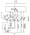
図4は、FPGA400上の非プログラマブルリソースから形成される中央処理装置(CPU)401を含むFPGA400を例示する。一実施例では、CPU401は、IBMのパワーPC405 CPUを含む。しかしながら、この発明は、いずれのCPUにも同様に適用可能である。さらに、この発明は、いくつの数のCPUとともに用いられてもよい。具体的には、図4に例示されるアーキテクチャが、FPGA上の各CPUに対して繰返され得る。
A. Central processing unit (CPU)
FIG. 4 illustrates an
この実施例では、CPU401は、ブロックランダムアクセスメモリ(BRAM)408Aおよび408B等の複数の「オンチップ」メモリと直接通信し得る。各CPUは、このようなオンチップメモリに対するプロプラエタリ接続およびそれ自体のポートを規定するため、これらの詳細は、ここで提供されない。
In this example,
CPU401は、任意の数の周辺モジュール、つまり、マスタモジュール406またはスレーブモジュール404によってCPU401に送られる「フラグ」を妨害および優先する割込コントローラ(INTC)409にも結合される。したがって、いずれかのスレーブモジュール404またはマスタモジュール406が、割込コントローラ409に結合され得る(線は図示せず)。これらのフラグは、CPU401からの即時アテンションを要求する周辺モジュールに関連した「イベント」を表す。この様態で、CPU401は、周辺モジュールの連続的なチェックを行なうことから解放され、CPU401が可能な限り効率的に動作し得ることが確実となる。たとえば、周辺モジュールからの1つのフラグは、CPU401に対して、ユーザがキーボード上の「入力」キーを押したことを知らせ得る。これらのフラグの生成は、当業者には周知であるため、ここで詳細に説明されない。周辺モジュールによって生成される割込に応答するために、CPU401は、PIC4
02およびOPB403を用いる(両方が以下で詳細に説明される)。
The
02 and OPB403 are used (both described in detail below).
なお、CPU401は、FPGAファブリックに対するCPU401の専用ピンアウトの結合を容易にする構造を含み得る。この発明は、異なる構造を有するさまざまなCPUとともに機能し得る。
Note that the
FPGA400は、複数の高速デバイス410およびマスタ/スレーブモジュール404/406からCPU401までのデータ転送を可能にする複数のデータ経路(図示せず)をさらに含む。したがって、図4に示される経路は、この発明に従ったトランザクション経路を示すことが意図される。
The
B.プログラマブルインターフェイスコア(PIC)
この発明に従うと、(FPGA400上およびチップ外の両方にある)他のデバイスとの高性能通信を提供するために、CPU401は、プログラマブルインターフェイスコア(PIC)402を用いる。プログラマブルインターフェイスコア402は、名前が示すように、FPGAソフトウェアツール(図3のFPGAソフトウェアツール306参照)によって生成されるコンフィギュレーションビットを用いてFPGA400上で実現される。1つの最適な実施例では、プログラマブルインターフェイスコア402は、クロスポイントスイッチを含み、クロスポイントスイッチは、(CPU401または高速バスインターフェイス(HSBI)407等の)いずれかのマスタデバイスがいずれかのスレーブデバイス410と通信することを選択的に可能にする。さらに、クロスポイントスイッチでは、第1のトランザクションが進行している間に、別のマスタデバイスが、同時に別のスレーブデバイスと通信することができる。この様態で、この発明は、FPGA400上およびチップ外の両方における、スレーブデバイスとマスタデバイスとの間の高性能インターフェイスを提供し得る。
B. Programmable interface core (PIC)
In accordance with the present invention, the
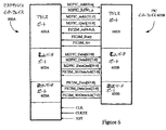
図4に示される実施例では、プログラマブルインターフェイスコア402は、4入力(マスタ)×4出力(スレーブ)(4×4)クロスポイントスイッチを用いて、マスタデバイスをスレーブデバイスに接続し得る。具体的には、マスタデバイスは、CPU401の命令キャッシュユニット(ICU)と、CPU401のデータキャッシュユニット(DCU)と、高速バスインターフェイス(HSBI)407と、OPBブリッジインモジュール(OPB/BI)とを含み得、スレーブデバイスは、DDR SDRAMコントローラデバイス410Aと、オフチップメモリ410B−410Dのうちの1つと、オンチップメモリ410E(一実施例では、BRAM)と、OPBブリッジアウトモジュール(OPB/BO)とを含み得る。NのマスタデバイスとMのスレーブデバイスとを有する他の実施例では、プログラマブルインターフェイスコア402は、N×Mクロスポイントスイッチとして構成され得る。しかしながら、重要なことには、他の種類のスイッチと比較して増大するクロスポイントスイッチ接続性のために、クロスポイントスイッチの実現は、FPGA400上の利用可能なリソースを最適化するように慎重に評価されなければならない。この評価は、以下で詳細に説明される。
In the example shown in FIG. 4, the
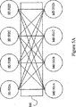
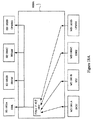
図5Aは、プログラマブルインターフェイスコアの一部として提供される、簡素化された4×4クロスポイントスイッチ500を例示し、クロスポイントスイッチ500は、4つのマスタデバイス501A−501Dおよび4つのスレーブデバイス502A−502Dを選択的に結合する。一実施例では、クロスポイントスイッチ400のサイズは、16×16スイッチにまで拡大され得る。なお、論理リソースによって、通例、クロスポイントスイッチのサイズが制限されるが、ルーティングリソースも制限的であり得る。したがって、クロスポイントスイッチの最大サイズは、FPGAに左右される。一実施例では、最大サイズは、PICを生成するために用いられるパラメータおよびN×Mサイズを考慮に入れて計算され得る。クロスポイントスイッチ500は、トランザクションのアドレス
およびデータ経路のための2つの別個の構造を含む。実際のFPGAでは、図5B(500A)および図5C(500B)を参照して説明されるこれらの構造は、オーバーラップするプログラマブルリソース上に置かれ得る。他の実施例では、トランザクションのアドレスおよびデータ論理内で用いられる構造は、オーバーラップしないプログラマブルリソースから形成される。
FIG. 5A illustrates a simplified 4 × 4
図5Bは、アドレス論理内のクロスポイントスイッチ(以下では、クロスポイントスイッチ500A)の一実現例のより詳細な図を示す。この実現例では、クロスポイントスイッチ500Aは、Nのアドレスデコーダ511(Nは、マスタデバイス501の数に等しい)と、Mのアクセスアービタ512(Mは、スレーブデバイス502の数に等しい)とを含む。マスタデバイス501A−501Dは、データキャッシュユニット(DCU)、命令キャッシュユニット(ICU)、高速バスインターフェイス(HSBI)、およびオンチップ周辺バスブリッジインモジュールOPB/BIを含む。スレーブデバイス502A−502Dは、DDRデバイス、スタティックランダムアクセスメモリ(SRAM)、ブロックRAM(BRAM)、およびOPBブリッジアウトマスタOPB/BOを含む。
FIG. 5B shows a more detailed diagram of one implementation of a crosspoint switch in address logic (hereinafter
OPB/BIおよびOPB/BOモジュールに関して、CPU401(図4)がスレーブモジュール404またはマスタ/スレーブモジュール405と通信する必要がある場合(以下で説明)、プログラマブルインターフェイスコア(PIC)402内のOPBブリッジアウトモジュールOPB/BOが、CPUのコマンドをOPB403に対して駆動することが注目される。しかしながら、PIC402の観点からは、このOBP/BOモジュールは、スレーブデバイスとして機能する。対照的に、マスタモジュール406またはマスタ/スレーブモジュール405がデバイス410に対してコマンドを発行する場合、その要求は、プログラマブルインターフェイスコア402内のブリッジインモジュールOPB/BIによって受取られる。したがって、PIC402の観点からは、OPB/BIは、マスタとして機能するように見える。したがって、OPB/BOおよびOPB/BIは、マスタ機能とスレーブ機能との両方を有するプログラマブルインターフェイスコア502内のブリッジモジュールとして特徴付けられ得る。OPB/BOMおよびOPB/BIは、図16および図17を参照しながらより詳細に説明される。
For OPB / BI and OPB / BO modules, if the CPU 401 (FIG. 4) needs to communicate with the slave module 404 or the master / slave module 405 (described below), the OPB bridge out in the programmable interface core (PIC) 402 It is noted that the module OPB / BO drives CPU commands to the
クロスポイントスイッチ500A内では、アクセスデコーダ511は、そのそれぞれのマスタデバイス501からアドレスを受取り、次に、アドレスをデコードして、マスタデバイスがどのスレーブデバイス502にアクセスすることを望むかを判断する。デコーディングの後、アドレスデコーダ511は、要求されたスレーブデバイス502に関連したアクセスアービタ512にアドレスを送る。多数のマスタデバイス501が1つのスレーブデバイス502にアクセスすることを望み得ることが思い出されたい。したがって、アクセスアービタ512を用いて、要求を行なうマスタデバイス間でプライオリティを決定する。アクセスアービタ512によって用いられ得るいくつかの公知のアルゴリズムは、シングルレベルラウンドロビン、マルチレベルラウンドロビン、最長時間未使用法、およびプライオリティベースのアプローチ(OPBバスアービタ503Aを参照しながら以下でより詳細に説明)を含む。なお、トランザクションは読出動作であるのか、または書込動作であるかということ、およびデータ転送サイズを含む、マスタデバイス501からの追加的な情報が、デコードされたアドレスとともにスレーブデバイス502に転送される。
Within
クロスポイントスイッチ500A内でアドレスデコーダ511およびアクセスアービタ512を用いることによって、前のトランザクションが完了する前に、マスタデバイス501が別のトランザクションを開始することが可能になる。言い換えると、デコードされたアドレスがアクセスアービタ512に一旦提供されると、アドレスデコーダ511は、次のアドレスをデコードし始め得る。この種のプロセスは、「トランザクションフォワー
ド」と呼ばれる。この発明は、トランザクションフォワードを有利に用いて、クロスポイントスイッチの性能を高める。
Using the address decoder 511 and access arbiter 512 within the
この発明の一実施例では、このトランザクションフォワード特徴は、(簡素化のために1つしか示されていない)多数のレジスタ513をアドレス論理内に含むことによって、さらに強化され得る。図5Bでは、これらのレジスタは、アドレスデコーダ511の前に、アドレスデコーダ511の後およびアクセスアービタ512の前に、および/または、アクセスアービタ512の後およびスレーブデバイス502の前に、置かれ得る。なお、追加的なレジスタが、アドレス論理内のいずれかのポイントに置かれ得る(しかしながら、各アドレス経路は、アドレス/制御経路において一貫したタイミングを保証するために、同じ場所にレジスタを有するべきである)。この発明では、これらのレジスタ513は、アドレスおよび制御情報のためにパイプライン方式を提供し得、したがって、他のトランザクションが処理されている間に、要求を行なうマスタが別のトランザクションを開始することが可能になる。したがって、この様態で、この発明のパイプライン方式は、システムの全アドレス/制御帯域幅を増大させることができ、多数のトランザクションのためのアドレス論理の速度を上げる。
In one embodiment of the invention, this transaction forward feature may be further enhanced by including a number of registers 513 (only one is shown for simplicity) in the address logic. In FIG. 5B, these registers may be placed before the address decoder 511, after the address decoder 511 and before the access arbiter 512, and / or after the access arbiter 512 and before the slave device 502. Note that additional registers may be placed at any point in the address logic (however, each address path should have a register in the same location to ensure consistent timing in the address / control path. is there). In the present invention, these
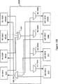
ある特定のスレーブデバイス502が、トランザクションに対して解放されているとアクセスアービタ512によって判断された後、そのアクセスアービタ512は、データ論理内で提供される構造と通信して、図5Cを参照しながら説明されるような適切な接続を生成する。図5Cは、データ論理のためのクロスポイントスイッチ(以下では、クロスポイントスイッチ500B)の一実現例のより詳細な図を示す。この実現例では、クロスポイントスイッチ500Bは、Nの書込マルチプレクサ514(Nは、書込動作において書込され得るスレーブデバイス502の数に等しい)と、Mの読出マルチプレクサ515(Mは、読出動作においてデータを受取り得るマスタデバイス501の数に等しい)とを含む。マルチプレクサ514A−514Dおよび515A−515Dは、アクセスアービタ512A−512D(図5B)によって制御される。
After the access arbiter 512 determines that a particular slave device 502 has been released for the transaction, the access arbiter 512 communicates with the structure provided in the data logic, see FIG. 5C. Create an appropriate connection as described in FIG. 5C shows a more detailed view of one implementation of a crosspoint switch for data logic (hereinafter
アドレス論理と同様に、クロスポイントスイッチ500Bは、レジスタ513によって提供されるパイプライン方式を含み得る。一実施例では、これらのレジスタ513は、マスタデバイス501と書込マルチプレクサ514との間に、および、スレーブデバイス502と読出マルチプレクサ515との間に置かれる。なお、追加的なレジスタがデータ論理内のいずれかのポイントに置かれ得る。しかしながら、各データ経路は、データ経路において一貫したタイミングを保証するために、同じ場所にレジスタを有するべきである。この発明では、これらのレジスタ513は、転送されるデータに対してパイプライン方式を提供し得、別の読出または書込トランザクションが処理されている間に、要求を行なうマスタまたはアクセスされるスレーブのいずれかが、別の読出または書込トランザクションを開始することが可能になる。したがって、この様態で、この発明のパイプライン方式は、システムの全データ帯域幅も増大させることができ、多数のトランザクションのデータ論理のスループットを上げる。
Similar to the address logic,
上述のように、この発明は、アドレスおよびデータ論理の両方においてトランザクションフォワードを有利に用い得る。パイプライン方式によって、トランザクションフォワードの最適化が可能になる。具体的には、マスタデバイスは、スレーブデバイスと直接通信しないため、パイプラインレジスタが、アドレス/データ論理内の多数の場所で提供され得る。したがって、一旦マスタデバイスがアドレスを送り出し、スレーブから肯定応答を受取ると、マスタデバイスは、そのトランザクションに関連した情報の残り(制御とデータとの両方)をパイプライン処理し得る。一旦スレーブデータ肯定応答信号がマスタに到達すると、マスタは、スレーブが実際にデータを受取るのを待たずにデータを供給できる点において、パイプライン方式は役立つ。この時点で、マスタデバイスは、別のトランザ
クションを開始できる。パイプライン化の量によって、同時にアクティブになり得るトランザクションの数が決定される。
As mentioned above, the present invention can advantageously use transaction forwarding in both address and data logic. The pipeline method enables optimization of transaction forward. Specifically, since the master device does not communicate directly with the slave device, pipeline registers can be provided at multiple locations within the address / data logic. Thus, once the master device sends out an address and receives an acknowledgment from the slave, the master device can pipeline the rest of the information associated with the transaction (both control and data). Once the slave data acknowledge signal reaches the master, the pipeline method is useful in that the master can supply the data without waiting for the slave to actually receive the data. At this point, the master device can begin another transaction. The amount of pipelining determines the number of transactions that can be active at the same time.
なお、全システム性能に関して、レイテンシ(つまり、このパイプライン方式に関連した遅延)も考慮されなければならない。たとえば、一実施例では、レジスタは、クロック信号を必要とするフリップフロップを用いて実現され得る。このクロック信号は、アドレスデコーダおよびアドレスアービタがそれらのそれぞれの機能を実行するために必要な時間に基づいてセットされ得る。なお、パイプライン方式は、周波数と直接相関関係がある。したがって、パイプライン化すればするほど、より高い周波数が提供される。しかしながら、周波数を増大させることは、また、レイテンシを望ましくないほど増大させる。したがって、以下にさらに詳細に説明されるように、この発明は、(パイプライン方式によって提供されるような)帯域幅とレイテンシとの間でバランスを確立する。 Note that latency (ie, delay associated with this pipeline method) must also be considered for overall system performance. For example, in one embodiment, the register may be implemented using flip-flops that require a clock signal. This clock signal may be set based on the time required for the address decoder and address arbiter to perform their respective functions. The pipeline method has a direct correlation with the frequency. Therefore, the higher the frequency, the higher the frequency provided. However, increasing the frequency also undesirably increases latency. Thus, as described in more detail below, the present invention establishes a balance between bandwidth and latency (as provided by a pipeline scheme).
別の利点として、この発明は、各スレーブデバイス内で提供される論理を大きく減じることができる。具体的には、この発明に関連するマスタデバイスと通信するスレーブデバイスは、アドレスデコードするために必要とされる複雑な回路をなくすことができる。したがって、この発明は、スレーブデバイスの設計、実現、および製造の作業を簡素化する。 As another advantage, the present invention can greatly reduce the logic provided within each slave device. Specifically, the slave device that communicates with the master device associated with the present invention can eliminate the complex circuitry required for address decoding. Thus, the present invention simplifies the work of designing, implementing and manufacturing slave devices.
対照的に、共有バスシステムでは、マスタデバイスは、アドレスをすべてのスレーブデバイスに一斉送信し得る。したがって、このシステムでは、各スレーブデバイスは、アドレスをデコードし、アドレスがそのスレーブデバイスに関係するかを判断するための論理を含み得る。アドレスがデコードされた後、適切なスレーブデバイスが信号をマスタデバイスに送り返し、これが、次に、トランザクションに関する情報の残りを、識別されたスレーブデバイスに送り得る。 In contrast, in a shared bus system, a master device can broadcast an address to all slave devices. Thus, in this system, each slave device may include logic to decode the address and determine whether the address is associated with that slave device. After the address is decoded, the appropriate slave device sends a signal back to the master device, which may then send the rest of the information about the transaction to the identified slave device.
上の説明から理解され得るように、共有バスシステムは、システム内に含まれ得るパイプラインの量を大きく制限し得る。たとえば、一旦マスタデバイスがアドレスを送り出すと、すべてのスレーブデバイスがアドレスをデコードしなければならず、他の指定されていないスレーブデバイスが、他のマスタデバイスとの他のトランザクションを進めることが妨げられる。したがって、先行技術の共有バスシステムは、本質的に、この発明のクロスポイントスイッチよりも低い性能を提供する。なお、(以下で説明される)ハイブリッドシステムでは、共有バス上のスレーブの数が制限され得る。この様態で、アドレスを一斉送信し、さらにはスレーブからの応答を待つ時間が、最小限にされ得る。言い換えると、高い帯域幅を必要とするデバイスは、共有バス構成に内在する余分なレイテンシを支え得るものと釣り合わされ得、ある特定のシステムが最適化される。 As can be appreciated from the above description, a shared bus system can greatly limit the amount of pipeline that can be included in the system. For example, once a master device sends out an address, all slave devices must decode the address, preventing other unspecified slave devices from proceeding with other transactions with other master devices. . Thus, the prior art shared bus system provides inherently lower performance than the crosspoint switch of the present invention. Note that in a hybrid system (described below), the number of slaves on a shared bus can be limited. In this manner, the time to broadcast addresses and wait for a response from the slave can be minimized. In other words, devices that require high bandwidth can be balanced with those that can support the extra latency inherent in a shared bus configuration, and certain systems are optimized.
この発明のスイッチファブリックとしてFPGA内のクロスポイントスイッチを構成することによって、いくつかの利点が提供される。第1に、クロスポイントスイッチは、「非閉塞的」であり、入力は、出力に対する非輻輳経路が保証されることが確実である。この局面は、この発明のパイプライン化されたアーキテクチャにおいて特に有利である。第2に、FPGAリソースを用いて実現されるクロスポイントスイッチによって、接続が迅速に、選択的に変更されることが可能となる。なお、このような接続の変更は、したがって、経路の変更も、他のいずれの経路の接続にも影響を及ぼさない。第3に、クロスポイントスイッチは、プログラマブルに「トリミング」されて、FPGA上で用いられるリソースを最小にし得る。 Configuring a crosspoint switch in an FPGA as the switch fabric of the present invention provides several advantages. First, the crosspoint switch is “non-blocking” and the input is guaranteed to be guaranteed a non-congested path to the output. This aspect is particularly advantageous in the pipelined architecture of the present invention. Second, the crosspoint switch implemented using FPGA resources allows connections to be quickly and selectively changed. It should be noted that such a connection change therefore does not affect the path change nor any other path connection. Third, the crosspoint switch can be programmably “trimmed” to minimize the resources used on the FPGA.
たとえば、図5Dは、アドレス/制御論理がトリミングされるクロスポイントスイッチ500Aの一実施例を示す。この実施例では、ユーザは、あるアドレス/制御論理が用いられないことを決定した。なお、ソフトウェアは、どの論理がトリミングされ得るかをユ
ーザが特定する助けとはなり得るが、このような決定をするためには、ユーザが通例、ソフトウェアに基本的なパラメータを提供しなければならない。この発明は、用いられない論理を除去し、その論理に関連するリソースがユーザの設計の他のコンポーネントのために用いられることを可能にする。代替的には、たとえユーザの設計の他のコンポーネントが、トリミングされた論理を用いない場合でも、ユーザの設計は縮小され得、おそらくは、より小さなFPGAが用いられるか、またはより多くのマスタまたはスレーブが同じサイズのFPGA内で実現されることさえも可能となる。図5Dでは、以下のアドレス/制御論理が除去される。すなわち、ICUからOPB/BO、HSBIからBRAM、HSBIからOPB/BO、OPB/BIからBRAM、およびOPB/BIからOPB/BOである。
For example, FIG. 5D shows one embodiment of a
別の例として、図5Eは、データ論理がトリミングされるクロスポイントスイッチ500Bの一実施例を示す。この実施例では、ユーザは、あるデータ論理が用いられないことを決定した。この発明は、用いられない論理を有利に除去し得る。図5Eでは、以下の書込データ論理が除去される。すなわち、HSBIからBRAMおよびOPB/BO、ICUからいずれかのスレーブデバイス(つまり、ICUはリードオンリデバイス)、OPB/BIからBRAMおよびOPB/BOである。加えて、この実施例では、以下の読出論理も除去される。すなわち、BRAMからHSBIおよびOPB/BI、およびOPB/BOからHSBIおよびOPB/BIである。
As another example, FIG. 5E shows one embodiment of a
この発明に従うと、いずれかの経路(および、関連の論理)のトリミングによって、残りの回路が簡素化され得る。たとえば、図5Eでは、書込マルチプレクサ514Cおよび514Dの各々は、1つの入力のみを有する。したがって、これらのマルチプレクサは、たとえば、簡素なパストランジスタとして実現され得る。読出マルチプレクサ515Cおよび515D等の他のマルチプレクサも簡素化され得る。論理を簡素化することによって、システムの速度および他の性能パラメータが改善され得る。したがって、この発明に従ったプログラマブルリソースをトリミングする能力によって、FPGAの性能および面積において、著しい改善が提供され得る。
In accordance with the present invention, trimming any path (and associated logic) can simplify the remaining circuitry. For example, in FIG. 5E, each of
この発明の一実施例では、クロスポイントスイッチ500A/500Bは、アドレス/制御論理がCLKで動作し、さらにはデータ論理がCLK2Xで動作するように、設計される。具体的には、スレーブデバイス502がトランザクションに利用可能であることが、アクセスアービタ512によって一旦判断されると、そのアクセスアービタ512は、適切な書込マルチプレクサ514または読出マルチプレクサ515を制御することによって、そのトランザクションのための必要な論理を生成し得る。したがって、この時点では、追加的な論理または経路変更が必要とされないため、書込または読出動作は、さらなる遅延を伴わずに進行することができる。したがって、一実施例では、アドレス/制御論理は、133MHzで動作し得、データ論理は、266MHzで動作し得る。 In one embodiment of the invention, the crosspoint switches 500A / 500B are designed so that the address / control logic operates on CLK and the data logic operates on CLK2X. Specifically, once the access arbiter 512 determines that the slave device 502 is available for a transaction, the access arbiter 512 controls the appropriate write multiplexer 514 or read multiplexer 515 to The necessary logic for the transaction can be generated. Thus, at this point, no additional logic or path changes are required, so the write or read operation can proceed without further delay. Thus, in one embodiment, the address / control logic can operate at 133 MHz and the data logic can operate at 266 MHz.
重要なことには、デュアルクロックシステムでは、制御経路は、公称データクロックレートの1/2で動作して、そのタスクを達成するための優先的な時間をこの経路に提供する。さらに、1/2対1比が存在するため、データレイテンシは、実質的に減じられ、データ転送周波数が上昇し得る。 Importantly, in a dual clock system, the control path operates at half the nominal data clock rate to provide this path with a preferential time to accomplish its task. Furthermore, since there is a 1/2 to 1 ratio, the data latency can be substantially reduced and the data transfer frequency can be increased.
なお、クロスポイントスイッチ500A/500Bは、1つ以上の特定の信号をマスタデバイス501に転送するための専用の追加的なラインを含み得る。これらの追加的なラインは、肯定応答信号を転送し得るが、転送に限定されているわけではない。たとえば、一実施例では、トランザクションフォワードは、要求を行なうマスタデバイス501に対してアクセスアービタ512により提供される肯定応答信号によって、トリガされ得る。具体的には、制御信号およびデータのパイプライン処理は、要求を行なうマスタデバイス
501が肯定応答信号を受け取った後に、開始される。
It should be noted that the
C.マスタおよびスレーブモジュール
この発明に従うと、通例、先行技術のシステム内では周辺デバイスとして提供される、マスタモジュール406とスレーブモジュール404との両方が、ユーザのトップレベル設計の一部として、またはコアとして、FPGA上に置かれ得る。この発明の一実施例では、FPGA400は、マスタとスレーブとの両方として働くハイブリッドモジュール405を含み得る。具体的には、ハイブリッドマスタ/スレーブモジュール405は、特定の時間期間中にトランザクションを開始し、オンチップ周辺バス(OPB)403を制御することができ、他の期間中は、トランザクションを受入れ、データをOPBバス403に提供し得る。たとえば、ネットワーキングアプリケーションでは、データパケットが、スレーブとしてのハイブリッドモジュール405によって受取られると、ハイブリッドモジュール405は、DMAを用いるマスタとしてパケットをメモリに送り得る。別の実施例では、マスタ機能は、スレーブモジュール内に組込まれる。
C. Master and Slave Modules According to the present invention, both the master module 406 and the slave module 404, typically provided as peripheral devices in prior art systems, are either part of the user's top-level design or as a core. It can be placed on an FPGA. In one embodiment of the invention,
有利なことには、この発明によって、パラメータ表示が容易にされるため、マスタおよびスレーブモジュールの数は、動的にさえも、変更され得る。したがって、この発明は、ユーザの設計を実現するために必要とされるFPGA上のリソースのみを用いる。 Advantageously, the present invention facilitates parameter display so that the number of master and slave modules can be changed even dynamically. Therefore, the present invention uses only the resources on the FPGA that are required to realize the user's design.
D.OPBバス
この発明に従うと、オンチップ周辺バス(OPB)403は、プログラマブルインターフェイスコア402とモジュール404/406との間の通信を容易にする接続インフラストラクチャを含む。OPB403は、複数のより低い性能の周辺デバイス、つまり、モジュール404/406をサポートする共有バスアーキテクチャを用いる。これらのモジュール404/406は、たとえば、シリアルポートおよびイーサネット(R)接続を用い得る。一実施例では、モジュール404/406は、IBMのコアコネクト(CoreConnect)(商標)OPB仕様に従い得る。
D. OPB Bus In accordance with the present invention, on-chip peripheral bus (OPB) 403 includes a connection infrastructure that facilitates communication between
重要なことには、OPB403は、FPGA400上に提供されるプログラマブルルーティングリソースから形成され得る。具体的には、バスのラインがプログラマブルルーティングリソースから形成され得、スイッチング論理は、CLB内のプログラマブルリソースから形成され得る。この様態で、OPB403は、FPGA400上のどこに位置付けられてもよい。さらに、OPB403は、いかなる数のモジュール404/406にも対応するように構成され得る。言い換えると、3つのマスタモジュール406および1つのスレーブモジュール404のみが、ユーザによってFPGA400上に置かれる場合、この発明は、これらの4つのモジュールのみのためのポートが作成されることを保証する。したがって、この発明に従うと、OPB403は、完全にパラメータ表示可能である。
Importantly,
OPB403は、単一のマスタモジュール406がスレーブモジュール404またはマスタ/スレーブ405と通信することを可能にするスイッチング論理を含む。具体的には、共有バスアーキテクチャのために、他のマスタモジュール406またはマスタ/スレーブ405は、各アクティブトランザクション中に、それらのそれぞれのスレーブモジュール404とのそれらのトランザクションを開始することを待たなければならない。これらのトランザクションにプライオリティを割当てるために、OPBアービタ403Aが提供される。
この発明の一実施例に従うと、OPBアービタ403Aは、いずれかの種類のアービトレーション方式を提供するように構成され得、さらにはFPGA400が動作しているときに動的に変化するようにさえも構成され得るコアである。なお、OPB403のように、OPBアービタ403Aは、完全にパラメータ表示可能である。したがって、OPBア
ービタ403Aは、ユーザによって指定された数のマスタモジュール406をアービトレートするために必要なFPGA400上のプログラマブルリソースのみを用いる。一般に、OPBアービタ403Aは、予め構築されたアルゴリズムを用いて、どのマスタモジュール406がOPB403を制御し得るかということと、その制御の時間期間とを決定する。
According to one embodiment of the present invention,
アービトレーションは、公平性とプライオリティという相反する目標を解決しなければならない。公平性は、1つのマスタモジュール406がOPB403を独占することを許可されるべきではないことを要求する。しかしながら、プライオリティは、特定の状況下では、予め定められたマスタモジュール406がより頻繁にOPB403を用いてタイムクリティカルな目標を達成すべきであることを要求する。OPBアービタ403Aによって用いられ得るいくつかの典型的なアルゴリズムは、シングルレベルラウンドロビン、マルチレベルラウンドロビン、最長時間未使用法、およびプライオリティベースのアプローチである。
Arbitration must solve the conflicting goals of fairness and priority. Fairness requires that one master module 406 should not be allowed to monopolize
シングルレベルラウンドロビンアプローチでは、小さな時間単位、つまり、量子が定義される。(特定のマスタ306に関連する)すべてのトランザクションが、巡回待ち行列内に置かれる。OPBアービタ403Aは、待ち行列に従い、マスタモジュールによるOPB403の使用を割当てて、1量子の時間間隔のためのトランザクションを達成し得る。待ち行列内の最後のトランザクションの後に、いずれかの新しいトランザクションが加えられ得る。
In the single level round robin approach, a small time unit, ie quantum, is defined. All transactions (related to a particular master 306) are placed in a circular queue. The
量子の終わりの前にトランザクションが終了すると、マスタモジュール406は、自発的にOPB403を解除し得る。しかしながら、トランザクションが量子の終わりにおいても依然として動作している場合、マスタモジュール406は、プリエンプトされ得、トランザクションは、待ち行列の終わりの部分に加えられ得る。なお、別の実施例では、マスタモジュール406は、そのトランザクションを完了することができる。このとき、OPBアービタ403Aは、OPB403を待ち行列内の次のトランザクションに割当て得る。
If the transaction ends before the end of the quantum, the master module 406 may voluntarily release the
マルチレベルラウンドロビンアプローチでは、少なくとも2つの巡回待ち行列が形成される。たとえば、第1の待ち行列と第2の待ち行列とが形成されると仮定すると、OPB403を頻繁に用いるトランザクションが、第1の待ち行列内に置かれ得、OPB403をそれほどは頻繁に用いないトランザクションが、第2の待ち行列内に置かれ得る。第2の待ち行列内のトランザクションは、同じ待ち行列内に存在するならば、OPB403に対して等しいアクセスを有し得る。しかしながら、第2の待ち行列内のトランザクションは、グループとして、第1の待ち行列内の各トランザクションと同等の、OPB403に対するアクセスを有し得る。言い換えると、第2の待ち行列のトランザクションは、「スーパートランザクション」を効率的に形成し、スーパートランザクションは、第1の待ち行列内のトランザクションのうちの1つであると考えられる。したがって、第1の待ち行列トランザクションのラウンドごとに、第2の待ち行列の1つのトランザクションが実行され得る。このアプローチでは、量子の終わりの前にトランザクションが終了すると、マスタモジュール406は、自発的にOPB403を解除し得る。しかしながら、トランザクションが量子の終わりにおいても依然として動作している場合は、マスタモジュール406は、プリエンプトされ得、トランザクションは、適切な待ち行列の終わりの部分に加えられ得る。
In the multi-level round robin approach, at least two cyclic queues are formed. For example, assuming that a first queue and a second queue are formed, transactions that frequently use
最長時間未使用法では、任意の待ち行列が形成される。OPBアービタ403Aは、最初は待ち行列に従い、待ち行列内の次のマスタモジュール406がOPB403の制御権を得ることを可能にする前に、各トランザクションを終了させ得る。しかしながら、OP
Bアービタ403Aが、待ち行列内において次ではないマスタモジュール406からバス制御の要求を受取った場合、OPBアービタ403Aは、最長時間未使用のOPB403を有したマスタモジュール406に対して(実行されているトランザクションの完了後に)OPB403の制御権を与え得る。
In the least recently used method, an arbitrary queue is formed. The
When the
最後に、プライオリティベースのアプローチでは、OPBアービタ403Aは、マスタモジュール406によって実行される関連のトランザクションのプライオリティにのみ基づいて、バス制御を決定し得る。このアプローチでは、より高いプライオリティの各トランザクションが、より低いプライオリティのトランザクションが開始許可され得る前に、完了し得る。一実施例では、プライオリティベースのアプローチは、FPGA内の性能に最も大きな影響を及ぼすマスタに対してプライオリティを許可することを含む。
Finally, in a priority-based approach, the
E.高速バスインターフェイス
この発明の一実施例に従うと、FPGA400は、バス407Aおよび407Bを介して、プログラマブルインターフェイスコア402とオフチップデバイス(図示せず)との間で多くの量のデータを転送することのできる高速バスインターフェイス(HSBI)407を含む。例示的なオフチップデバイスは、ギガビットI/O、高速I/O、PCI-X、または他の公知の高性能プロトコルを用いて、インターフェイス407と通信し得る。このインターフェイス407は、コアの形で提供され得る。なお、転送されるデータは、(フラッシュメモリ、SRAMメモリ、および/または別の種類のメモリ等の)オフチップメモリまたは(BRAM等の)オンチップメモリから、またはそこへと、転送され得る。
E. High Speed Bus Interface According to one embodiment of the present invention, the
一実施例では、HSBI407は、バス407Cを通って非データ移動のためにアドレス指定され得る。これらのバスは、CPU401または他のバスマスタが、HSBI407の内部レジスタセットに対する局所的なアクセスを有することを可能にする。たとえば、HSBI407は、INTC409に対する割込を生成して、それがデータパケットを受取り、さらにはそれを外部のDDRメモリデバイスに転送することを完了したことを示し得た。CPU401は、割込に応答するとき、バス407Aを用いてHSBI407と対話(talk)して、サービスに対するその要求が何についてであるかを把握し得る。しかしながら、バス407Aを用いる行為は、いずれの進行中のデータ移動動作も割込まれる必要があり得ることを意味する。したがって、一実施例では、テリアリ(teriary)バス407Cセットが、OPB403に対するマスタおよびスレーブ動作の両方のために存在する。バス407Cを用いることにより、CPU401は、バス407A上のデータ移動に影響を与えずにHSBI407と対話できる。さらに、HSBI407がデータをデバイス404Cに移動させたい場合、それは、まずPIC402にアクセスする必要なしに、および/または、それをメモリに記憶することなく、それを行ない得る。むしろ、HSBI407は、OPB403上でトランザクションを開始し、データを直接転送することができ、データをダブルバッファする必要性をなくし、システム全体の著しい性能向上に貢献する。
In one embodiment,
V.FPGA実現例:詳細
A.PICおよびデバイス:ポート、タイミング、および実施例
マスタデバイスおよびスレーブデバイスは、よりモジュラな設計を可能にする包括的インターフェイスを用いる。具体的には、これらのモジュールは、プログラマブルインターフェイスコアに「プラグイン」され得る包括的なポート(以下で詳細に説明)を用いる。ここでの説明では、用語「ポート」は、マスタ/スレーブデバイスとプログラマブルインターフェイスコアとの間に提供される信号セットを含み得る。これらの包括的ポートのため、いかなる数のマスタデバイスおよびスレーブデバイスが、いずれの組合せで、この発明に含まれてもよい。一実施例では、NのマスタデバイスとMのスレーブデバイスとが、
プログラマブルインターフェイスコアに結合され、NおよびMは、1以上の整数である(いくつかの事例では、同じ整数である)。
V. FPGA implementation example: details PICs and Devices: Ports, Timing, and Examples Master and slave devices use a comprehensive interface that allows for a more modular design. Specifically, these modules use generic ports (described in detail below) that can be “plugged in” to the programmable interface core. In the description herein, the term “port” may include a set of signals provided between a master / slave device and a programmable interface core. Because of these generic ports, any number of master and slave devices may be included in this invention, in any combination. In one embodiment, N master devices and M slave devices are:
Coupled to the programmable interface core, N and M are integers greater than or equal to 1 (in some cases, the same integer).
なお、この発明では、より多くの機能を提供する複雑なプロトコルとより速く実行され得る簡潔なプロトコルとの間で、正しいバランスを選ぶことの重要性が認識される。ここで詳細に説明される実施例では、比較的簡素なプロトコルが用いられ、依然として大部分のタスクを達成しながらも、非常に速く実行される。 It should be noted that the present invention recognizes the importance of choosing the right balance between complex protocols that provide more functions and simple protocols that can be executed faster. In the embodiment described in detail herein, a relatively simple protocol is used, which executes very quickly while still accomplishing most tasks.
1.マスタデバイスとPICとの間の通信
図6は、いずれかのマスタデバイスとプログラマブルインターフェイスコアとの間で転送され得る典型的な信号を例示する。この転送を容易にするために、マスタデバイスは、アドレスポート601A、書込データポート602A、および読出データポート603Aを有するインターフェイス600Aを含む。同様の構成で、プログラマブルインターフェイスコアは、アドレスポート601B、書込データポート602B、および読出データポート603Bを有するPICインターフェイス600Bを含む。一実施例では、ポート間で転送される各信号(または、信号セット)は、関連のライン/バスを有し、その信号の効率的な転送を容易にする。なお、ここでの説明では、信号の名称は、関連のライン/バスも指し得る。以下に説明される実施例に従うと、標準のPLBプロトコルが制限され、より少ない機能が提供されるが、FPGAがずっと速く動作することが可能になる。
1. Communication between Master Device and PIC FIG. 6 illustrates exemplary signals that may be transferred between any master device and the programmable interface core. To facilitate this transfer, the master device includes an
a.マスタのためのアドレスポート
アドレスポート601Aは、以下の信号を出力し得る。
a. Address Port for Master The
M2PIC_AddrReq
このステータス信号は、マスタがデータ転送を要求することを望むことを表す。なお、M2PIC_AddrReqがアクティブである場合、他の信号、具体的には、M2PIC_Addr[31:0]、M2PIC_AddrQual、およびM2PIC_RdWr_nも有効でなければならない。この発明の一実施例では、論理1信号(1)が、要求はペンディングであることを表し、論理0(0)信号が、1つの要求もペンディングでないことを表す。この信号は、中位のタイミングの信号として特徴づけられ、CLKのクロックドメインを有する。
M2PIC_AddrReq
This status signal indicates that the master wants to request data transfer. Note that if M2PIC_AddrReq is active, other signals, specifically M2PIC_Addr [31: 0], M2PIC_AddrQual, and M2PIC_RdWr_n must also be valid. In one embodiment of the invention, a
M2PIC_Addr[0:31]
この32ビット信号は、アドレス、つまり、要求される転送の、メモリスペース内の特定のバイトを表す。上述のように、この信号は、M2PIC_AddrReqが有効である同じサイクル上で有効でなければならない。このバスは、クリティカルパス上にある。なぜならば、それは、プログラマブルインターフェイスコアのためのアドレスデコーダ(たとえば、図5Bのアドレスデコーダ511参照)に信号を与えるためである。したがって、一実施例では、上位ビットのみが実際には比較され、下位のビットは、中位のタイミングを有するとして扱われ得る。具体的には、上位ビットは、スレーブのアドレスを識別し、下位ビットは、スレーブ内の目標メモリを識別する。したがって、スレーブの識別が本発明のアービトレーションに先行し(たとえば、図5Bのアクセスアービタ512を参照)、いずれかの1つの時間期間中に、1つのトランザクションのみがスレーブ内でアクティブになり得るため、上位ビットの読出しは、遅いタイミングとして特徴づけられるべきであり、スレーブ内の実際の記憶場所は、中位のタイミングとして特徴づけられ得る。
M2PIC_Addr [0:31]
This 32-bit signal represents the address, ie a specific byte in the memory space of the requested transfer. As mentioned above, this signal must be valid on the same cycle that M2PIC_AddrReq is valid. This bus is on the critical path. This is because it provides a signal to an address decoder for the programmable interface core (see, for example, address decoder 511 in FIG. 5B). Thus, in one embodiment, only the upper bits are actually compared, and the lower bits can be treated as having intermediate timing. Specifically, the upper bit identifies the address of the slave and the lower bit identifies the target memory within the slave. Thus, slave identification precedes arbitration of the present invention (see, eg, access arbiter 512 in FIG. 5B), and only one transaction can be active in the slave during any one time period. The upper bit read should be characterized as late timing, and the actual memory location in the slave can be characterized as medium timing.
なお、要求されるデータ転送は、好ましくは、転送サイズに対してアドレスアラインされる。たとえば、8ワード転送では、アドレスは8ワード境界上にあるべきである。言い換えると、2ワード転送は、論理アドレス0、2、4等で始まり得、4ワード転送は、論理アドレス0、4、8等で始まり得、8ワード転送は、論理アドレス0、8、16等で始
まり得る(例外として、目標ワード第1転送(target word first transfer)を特定する場合、アラインされていないアドレスが与えられ得る)。アライメントは、DDR SRAMのようなデバイスのために必要とされる。なぜならば、これらのデバイスは、アラインされたブロック転送を実行するように設計されているためである。この信号は、CLKのクロックドメインを有する。
Note that the requested data transfer is preferably address aligned with the transfer size. For example, in an 8-word transfer, the address should be on an 8-word boundary. In other words, a 2-word transfer may start with
M2PIC_RdWr_n
この信号は、アドレス要求信号(M2PIC_AddrReq)に付随するための読出または書込フラグを提供する。上述のように、この信号は、M2PIC_AddrReqが有効である同じサイクル上で有効でなければならない。一実施例では、論理1信号(1)が、読出動作が要求されることを表し、論理0(0)信号が、書込動作が要求されることを表す。この信号は、中位のタイミングの信号として特徴づけられ、CLKのクロックドメインを有する。
M2PIC_RdWr_n
This signal provides a read or write flag to accompany the address request signal (M2PIC_AddrReq). As mentioned above, this signal must be valid on the same cycle that M2PIC_AddrReq is valid. In one embodiment, a
M2PIC_AddrQual[16:0]
このアドレス転送修飾子信号は、プロプラエタリCPU、一実施例では、IBMのパワーPC405に特有である。上述のように、この信号は、M2PIC_AddrReqが有効である同じサイクル上で有効でなければならない。これらの信号は、プログラマブルインターフェイスコアによってデコードまたは処理されず、適切なスレーブデバイスへとルーティングされるだけである。この信号は、中位のタイミングの信号として特徴づけられ、CLKのクロックドメインを有する。この信号のためのビット定義は、以下のとおりである。
M2PIC_AddrQual [16: 0]
This address transfer modifier signal is specific to the proprietary CPU, in one embodiment, the IBM Power PC 405. As mentioned above, this signal must be valid on the same cycle that M2PIC_AddrReq is valid. These signals are not decoded or processed by the programmable interface core, but are only routed to the appropriate slave device. This signal is characterized as a medium timing signal and has a clock domain of CLK. The bit definition for this signal is as follows:
なお、32ビットシステムでは、ユーザは、32ワードバーストモードをサポートする
ことを望まない場合もある。なぜならば、これは、FPGAプリミティブに効率的にマッピングしない構造を必要とし得るためである。
Note that in 32-bit systems, the user may not want to support 32-word burst mode. This is because it may require a structure that does not map efficiently to FPGA primitives.
バイトイネーブルがシングルビート(つまり、1または2ワード)転送に提供されて、CPUのようなデバイスが、バイトおよびハーフワード読出のようなより小さなサイズの読出を実行することを可能にする。この機能は、たとえば、(図16および図17を参照しながら詳細に説明される)OPBブリッジ内で特に重要である。なぜならば、いくつかのOPBデバイス(特に、スレーブ)は、バイト長レジスタのみを有し得るためである。DRAMまたはSRAM等のメモリデバイスにとっては、たとえバイトのみが必要とされている場合でも、ワードまたはダブルワードで読出すことに問題はなく、これらのデバイスは、シングルビート転送バイトイネーブルを無視し得る。これらのバイトイネーブルビットは、情報がデータ経路バイトイネーブルに対して冗長ではあるが、書込に対しても有効である。 A byte enable is provided for single beat (ie, 1 or 2 word) transfers to allow devices such as CPUs to perform smaller size reads such as byte and halfword reads. This function is particularly important within an OPB bridge (described in detail with reference to FIGS. 16 and 17), for example. This is because some OPB devices (especially slaves) may only have byte length registers. For memory devices such as DRAM or SRAM, there is no problem reading in words or double words, even if only bytes are needed, and these devices can ignore single beat transfer byte enables. These byte enable bits are useful for writing, although the information is redundant to the data path byte enable.
アドレスポート601Aは、以下の信号を受取ることもできる。
PIC2M_AddrAck
(プログラマブルインターフェイスコアからの)このストローブ信号は、現在のアドレスを肯定応答し、もしあれば、次のアドレス要求をフェッチする。PIC2M_AddrAckがアサートされた後のサイクル上で、M2PIC_AddrReq、M2PIC_Addr、M2PIC_RdWr_n、およびM2PIC_AddrQualが更新される。この信号は、アドレス要求当たり、1CLKサイクルだけアサートされる。この信号は、遅いタイミングの信号として特徴づけられ、CLKのクロックドメインを有する。
PIC2M_AddrAck
This strobe signal (from the programmable interface core) acknowledges the current address and fetches the next address request, if any. On the cycle after PIC2M_AddrAck is asserted, M2PIC_AddrReq, M2PIC_Addr, M2PIC_RdWr_n, and M2PIC_AddrQual are updated. This signal is asserted for 1 CLK cycle per address request. This signal is characterized as a late timing signal and has a clock domain of CLK.
PIC2M_Busy
この信号は、要求しているマスタに対して、そのトランザクションのうちの1つがスレーブ内で進行していることを伝える。この信号は、プログラマブルインターフェイスコアがそのPIC2M_AddrAckを発行した後に、ハイとなり、スレーブが(以下で詳細に説明される)そのS2PIC_RdXferDoneまたはS2PIC_WrXferDone信号をアサートしたときにローに戻って、データ転送がスレーブによって完了したことを表す。一実施例では、PIC2M_Busy信号およびマスタのM2PIC_AddrReq信号が、ORゲートに提供される。この様態で、マスタは、それがプログラマブルインターフェイスコア上のすべてのそのトランザクションをいつ完了したかを判断し得る。この信号は、“Sync”または“EIEIO”(エンフォース命令実行インオーダ(Enforce Instruction Execution In Order))命令をCPU内でサポートする。一実施例では、論理1は、プログラマブルインターフェイスコアがデータ転送でビジーであることを示し、論理0は、進行中のトランザクションが存在しないことを示す。なお、スレーブは、それがトランザクションを内部で完了していない場合、それがS2PIC_RdXferDone/S2PIC_WrXferDoneをアサートした後、信号PIC2M_Busyをアクティブに保持することが許可されている。この信号は、中位のタイミングの信号として特徴づけられ、CLKのクロックドメインを有する。
PIC2M_Busy
This signal tells the requesting master that one of its transactions is in progress in the slave. This signal goes high after the programmable interface core issues its PIC2M_AddrAck and returns low when the slave asserts its S2PIC_RdXferDone or S2PIC_WrXferDone signal (described in detail below), completing the data transfer by the slave Represents that In one embodiment, the PIC2M_Busy signal and the master M2PIC_AddrReq signal are provided to the OR gate. In this manner, the master can determine when it has completed all its transactions on the programmable interface core. This signal supports "Sync" or "EIEIO" (Enforce Instruction Execution In Order) instructions in the CPU. In one embodiment, a
PIC2M_Err
この信号は、マスタに対して、その進行中のトランザクションのうちの1つがエラーを生じさせたことを伝える。読出エラーに対しては、この信号は、(以下で説明される)PIC2M_RdDataAckとともにアクティブになり得る。書込エラーに対しては、この信号は、プログラマブルインターフェイスコア上のトランザクション中またはその後に、アサートされ得る。より具体的には、PIC2M_Busy信号がアクティブなままである限り、書込トランザクションがプログラマブルインターフェイスコア上で完了した後に、エラー信号がアサートされ得るのみである。この時点で、要求を行なっているマス
タは、エラーレジスタ、つまり、スレーブのBEARおよびBESRを調べて、エラーは何であったのかを判断し得る。この信号は、遅いタイミングの信号として特徴づけられ、CLK2Xのクロックドメインを有する。
PIC2M_Err
This signal tells the master that one of its ongoing transactions has caused an error. For read errors, this signal can be active with PIC2M_RdDataAck (described below). For write errors, this signal may be asserted during or after a transaction on the programmable interface core. More specifically, as long as the PIC2M_Busy signal remains active, the error signal can only be asserted after the write transaction is completed on the programmable interface core. At this point, the requesting master can examine the error register, ie, the slave's BEAR and BESR, to determine what the error was. This signal is characterized as a late timing signal and has a clock domain of CLK2X.
b.マスタのための書込ポート
この発明に従うと、マスタは、それが転送要求している全書込データを、それが供給できることを確信していなければならない。データフロー制御信号は存在しないため、マスタは、転送されているデータの流れを遅くする、または中断することはできない。しかしながら、スレーブデバイスは、データ肯定応答信号(つまり、PIC2M_WrData
Ack)を遅らせる(hold off)ことによって、データ転送間で待機状態を強制することができる。これらの制約の観点から、マスタ書込ポート602Aは、以下の信号を出力し得る。
b. Write Port for Master According to the present invention, the master must be confident that it can supply all the write data it is requesting to transfer. Since there is no data flow control signal, the master cannot slow down or interrupt the flow of data being transferred. However, the slave device does not accept the data acknowledge signal (ie, PIC2M_WrData
By delaying (Ack) (hold off), a standby state can be forced between data transfers. In view of these constraints, the master write port 602A can output the following signals.
M2PIC_Data
この信号は、書込転送データを提供する。一般に、転送されるべき書込データの第1の部分は、対応のアドレス要求がスレーブに到達する機会を持つときまでに、利用可能である。一実施例では、アドレスデータがプログラマブルインターフェイスコアをパイプライン方式で通る(pipeline through)ために2つのCLK(または、4つのCLKX2)サイクルのレイテンシが存在する。したがって、アドレス要求が発行された後、書込データは、2つのCLKサイクルに対して準備ができているべきである。なお、スレーブが書込に対して所与の最小応答時間を有するカスタムシステムでは、書込データのアベイラビリティは、この量だけ遅延され得る。
M2PIC_Data
This signal provides write transfer data. In general, the first part of the write data to be transferred is available by the time the corresponding address request has an opportunity to reach the slave. In one embodiment, there is a latency of two CLK (or four CLKX2) cycles for the address data to pipeline through the programmable interface core. Thus, after the address request is issued, the write data should be ready for two CLK cycles. Note that in a custom system where the slave has a given minimum response time for writing, the availability of the write data can be delayed by this amount.
一実施例では、書込転送データは、64ビットを含む。しかしながら、他の実施例では、より少ない、またはより多くのビットが用いられ得る。いずれの場合も、書込転送データを運ぶバスは、最適な幅にまでスケールダウン/アップされ得る。なお、このバスは、プログラマブルインターフェイスコアにおいて長い距離に及び得るため、そのタイミングが重要である。したがって、この信号は、遅いタイミングの信号として特徴づけられ、CLK2Xのクロックドメインを有する。 In one embodiment, the write transfer data includes 64 bits. However, in other embodiments, fewer or more bits may be used. In either case, the bus carrying the write transfer data can be scaled down / up to the optimum width. Note that the timing of this bus is important because it can span a long distance in the programmable interface core. Therefore, this signal is characterized as a late timing signal and has a clock domain of CLK2X.
M2PIC_DataBE[7:0]
この書込転送データバイトイネーブル信号は、M2PIC_Data信号と同じタイミングを有し、バイトイネーブル修飾子として書込データに付随する。一実施例では、インターリーブドビットまたはオールビットオフを含むいずれかのバイトイネーブルパターンが許容される。たとえば、高速マスタは、16ワードバースト転送を開始し、第1のデータ転送上ですべてのバイトイネーブルをオフにして、3動作ではなく1動作で14ワードバーストを効率的に実行し得る(8ワードバースト+4ワードバースト+1ダブルワード)。この信号は、32ビットPICシステム内では4ビット幅であり得る。この信号は、遅いタイミングの信号として特徴づけられ、CLK2Xのクロックドメインを有する。
M2PIC_DataBE [7: 0]
This write transfer data byte enable signal has the same timing as the M2PIC_Data signal, and accompanies the write data as a byte enable modifier. In one embodiment, any byte enable pattern including interleaved bits or all bit off is allowed. For example, a high speed master may initiate a 16 word burst transfer, turn off all byte enables on the first data transfer, and efficiently perform a 14 word burst in one operation instead of three operations (8 words Burst + 4 word burst + 1 double word). This signal may be 4 bits wide in a 32 bit PIC system. This signal is characterized as a late timing signal and has a clock domain of CLK2X.
M2PIC_DataQual[N:0]
この信号は、追加的な情報が書込データおよび/または書込バイトイネーブルとともに転送されることを可能にする。たとえば、一実施例では、パリティまたはエラー訂正コードビットが、書込データとともに転送され得る。なお、各M2PIC_DataQual信号は、各データとともに変化し得る。この信号は、遅いタイミングの信号として特徴づけられ、CLK2Xのクロックドメインを有する。
M2PIC_DataQual [N: 0]
This signal allows additional information to be transferred with the write data and / or write byte enable. For example, in one embodiment, parity or error correction code bits may be transferred along with the write data. Each M2PIC_DataQual signal can change with each data. This signal is characterized as a late timing signal and has a clock domain of CLK2X.
PIC2M_WrDataAck[7:0]
このストローブは、書込データを肯定応答し、次のデータ部分が転送されることを可能にする。PIC2M_WrDataAck信号がアサートされた後のサイクル上では、も
しあれば、次のデータが駆動されなければならない。各PIC2M_WrDataAckビット(この実施例では、合計8ビット)は、その対応のバイトレーンのデータを肯定応答する。この様態で、より小さな幅またはより遅いスレーブが、一度にいくつかのバイトレーンを肯定応答できる。しかしながら、たとえバイトイネーブルビットがそのバイトレーンのためにセットされていなくても、トランザクションは、すべてのバイトレーンに対して肯定応答される。この様態で、マスタは、データが適切に書込まれたことを知る。PIC2M_WrDataAck信号の動的な性質は有利である。なぜならば、それによって、データが転送において連続しないことが可能となるためである。一実施例では、PIC2M_WrDataAckビットは、増加するバイトアドレスの順序で(つまり、システムに応じて、ビット[7]から[0]、または[0]から[7]で)サイクルする。32ビットシステムでは、この信号は、4ビット幅であり得る。この信号は、遅いタイミングの信号として特徴づけられ、CLK2Xのクロックドメインを有する。
PIC2M_WrDataAck [7: 0]
This strobe acknowledges the write data and allows the next data portion to be transferred. On the cycle after the PIC2M_WrDataAck signal is asserted, the next data, if any, must be driven. Each PIC2M_WrDataAck bit (in this example, a total of 8 bits) acknowledges the data in its corresponding byte lane. In this manner, a smaller or slower slave can acknowledge several byte lanes at a time. However, the transaction is acknowledged for all byte lanes even if the byte enable bit is not set for that byte lane. In this manner, the master knows that the data has been properly written. The dynamic nature of the PIC2M_WrDataAck signal is advantageous. This is because it makes it possible for the data not to be continuous in the transfer. In one embodiment, the PIC2M_WrDataAck bits cycle in increasing byte address order (ie, bits [7] to [0], or [0] to [7], depending on the system). In a 32-bit system, this signal can be 4 bits wide. This signal is characterized as a late timing signal and has a clock domain of CLK2X.
c.マスタのための読出ポート
読出動作では、マスタデバイスは、それが転送要求している全データを、それが受取ることができることを確信していなければならない。データフロー制御信号は存在しないため、マスタデバイスは、転送されているデータの流れを遅くする、または中断することはできない。しかしながら、スレーブデバイスは、データ肯定応答信号(つまり、PIC2M_RdDataAck)を遅らせる(hold off)ことによって、データ転送間で待機状態を強制することができる。
c. Read Port for Master In a read operation, the master device must be sure that it can receive all the data it is requesting to transfer. Since there is no data flow control signal, the master device cannot slow down or interrupt the flow of data being transferred. However, the slave device can force a wait state between data transfers by holding off the data acknowledgment signal (ie, PIC2M_RdDataAck).
読出ポート603Aは、以下の信号を受取り得る。 Read port 603A may receive the following signals.
PIC2M_Data
この信号は、転送されるべき読出データを含む。一実施例では、これは、64ビットのデータを含む。別の実施例では、より少ない、またはより多くのビットが転送され得る。いずれの場合にも、この信号バスを転送しているバスは、適切なサイズにスケールダウン/アップされ得る。このバスは、プログラマブルインターフェイスコアにおいて長い距離に及び得るため、そのタイミングは、重要である。したがって、この信号は、遅いタイミングの信号として特徴づけられ、CLK2Xのクロックドメインを有する。
PIC2M_Data
This signal contains the read data to be transferred. In one embodiment, this includes 64 bits of data. In other embodiments, fewer or more bits may be transferred. In either case, the bus transferring this signal bus can be scaled down / up to an appropriate size. The timing is important because this bus can span a long distance in the programmable interface core. Therefore, this signal is characterized as a late timing signal and has a clock domain of CLK2X.
PIC2M_DataQual
この信号は、読出データ転送修飾子を指す。一実施例では、ビット定義は、以下のとおりである。
PIC2M_DataQual
This signal points to the read data transfer modifier. In one embodiment, the bit definitions are as follows:
なお、一実施例では、CPUは、サイズにおいて最大32ワードの転送を要求し得る。したがって、5ビットの「読出ワードアドレス」が、CPUをサポートするために必要とされる(論理的に、この信号は、32ワードよりも大きな転送を定義できない)。この信号は、遅いタイミングの信号として特徴づけられ、CLK2Xのクロックドメインを有する。 Note that in one embodiment, the CPU may request a transfer of up to 32 words in size. Thus, a 5 bit “read word address” is required to support the CPU (logically this signal cannot define a transfer larger than 32 words). This signal is characterized as a late timing signal and has a clock domain of CLK2X.
PIC2M_RdDataAck[7:0]
この読出ストローブ信号は、読出データが受取られることを許可する。各PIC2M_RdDataAckビットは、その対応のバイトレーンのためのデータを個別に肯定応答し、より小さな幅またはより遅いスレーブが一度に数個のバイトレーンを肯定応答することを可能にする。スレーブは、たとえバイトイネーブルビットがそのバイトレーンに対してセットされていなくても、すべてのバイトレーンが肯定応答されることを保証する。加えて、増加するバイトアドレスの順序で(これは、システムがビッグエンディアンまたはリトルエンディアンであるかに応じて、ビット[7]から[0]、または[0]から[7]になり得る)、スレーブは、PIC2M_RdDataAckビットをサイクルし得る。結果として、32ビットPICシステムでは、この信号は、4ビット幅になり得る。この信号は、遅いタイミングの信号として特徴づけられ、CLK2Xのクロックドメインを有する。
PIC2M_RdDataAck [7: 0]
This read strobe signal allows read data to be received. Each PIC2M_RdDataAck bit individually acknowledges the data for its corresponding byte lane, allowing a smaller or slower slave to acknowledge several byte lanes at a time. The slave ensures that all byte lanes are acknowledged even if the byte enable bit is not set for that byte lane. In addition, in increasing byte address order (this can be bits [7] to [0], or [0] to [7], depending on whether the system is big endian or little endian) The slave may cycle the PIC2M_RdDataAck bit. As a result, in a 32-bit PIC system, this signal can be 4 bits wide. This signal is characterized as a late timing signal and has a clock domain of CLK2X.
2.マスタデバイスのタイミング
図7は、マスタデバイスが、8ワード書込動作を生成し、次に8ワード読出動作を生成するタイミング図を示す。書込動作では、マスタは、時間t1においてアドレス要求(m_addr_req)をアサートする。同時に、マスタは、トランザクションが書込動作であることを示し(m_addr_r_wnがローに遷移する)、書込アドレス(m_addr[31:0])および転送サイズならびに他のいずれかの修飾子(m_addr_qual[])を送る。
2. Master Device Timing FIG. 7 shows a timing diagram in which the master device generates an 8-word write operation and then generates an 8-word read operation. In a write operation, the master asserts an address request (m_addr_req) at time t1. At the same time, the master indicates that the transaction is a write operation (m_addr_r_wn transitions low), the write address (m_addr [31: 0]) and transfer size and any other qualifier (m_addr_qual [] )
1クロック(clk)サイクルのレイテンシ後(レイテンシは、他の実施例では異なり得る)、マスタは、時間t3においてプログラマブルインターフェイスコアからアドレス肯定応答(m_addr_ack)を受取り、マスタが時間t5において別のトランザクションを開始することを可能にする。なお、時間t1において、マスタは、書込データ(D1w)を送るが、時間t3においてのアドレス肯定応答(m_addr_ack)の受取り後まで待機してから、時間t3、t4、およびt5において書込データの残り(D2w、D3w、およびD4w)を引き続き送る(1DDRクロック(clk2x)サイクルのレイテンシ)。(この実施例では、ワードは、32ビットに等しい。したがって、64ビットデータ経路では、4つの64ビット転送のみが必要とされる。)
図7では、読出動作が書込動作の直後に続く。したがって、アドレス要求(m_addr_req)は、論理1のままである。しかしながら、マスタは、トランザクションが読出動作であることを示さなければならない。したがって、m_addr_r_wnは、時間t5においてハイに遷移する。この発明の一実施例のパイプライン方式に従うと、時間t5において、つまり、書込動作が時間t7で完了する前に、マスタは、読出アドレス(m_addr[31:0])およびアドレス修飾子(m_addr_qual[])を送り得る。マスタデバイスは、時間t8で開始し、かつ時間t12で終了する読出修飾子(Q1r、Q2r、Q3r、およびQ4r)および読出データ(D1r、D2r、D3r、およびD4r)を受取る。
After a latency of one clock (clk) cycle (latency may be different in other embodiments), the master receives an address acknowledgment (m_addr_ack) from the programmable interface core at time t3, and the master performs another transaction at time t5. Allows you to start. At time t1, the master sends write data (D1w), but after waiting for the address acknowledgment (m_addr_ack) at time t3, the master transmits the write data at time t3, t4, and t5. Continue to send the rest (D2w, D3w, and D4w) (1 DDR clock (clk2x) cycle latency). (In this example, a word is equal to 32 bits. Therefore, in a 64-bit data path, only four 64-bit transfers are required.)
In FIG. 7, the read operation continues immediately after the write operation. Therefore, the address request (m_addr_req) remains at logic one. However, the master must indicate that the transaction is a read operation. Therefore, m_addr_r_wn transitions high at time t5. According to the pipeline scheme of one embodiment of the present invention, at time t5, that is, before the write operation is completed at time t7, the master reads the read address (m_addr [31: 0]) and the address qualifier (m_addr_qual). []) Can be sent. The master device receives read qualifiers (Q1r, Q2r, Q3r, and Q4r) and read data (D1r, D2r, D3r, and D4r) starting at time t8 and ending at time t12.
3.スレーブデバイスとPICとの間の通信
スレーブデバイスは、データを転送するためのコマンドを受取り、マスタデバイスが要求する読出動作または書込動作を実行する。図8は、スレーブデバイスとプログラマブルインターフェイスコアとの間で転送され得る典型的な信号を示す。この転送を容易にするために、スレーブデバイスは、アドレスポート801A、書込データポート802A、および読出データポート803Aを有するインターフェイス800Aを含む。同様の構成で、プログラマブルインターフェイスコアは、アドレスポート801B、書込データポート802B、および読出データポート803Bを有するPICインターフェイス800Bを含む。なお、いくつかの信号は、マスタポートのためのそれら(図6)と類似しており、それらの信号の方向が逆になっている。
3. Communication between slave device and PIC The slave device receives a command for transferring data, and executes a read operation or a write operation requested by the master device. FIG. 8 shows exemplary signals that may be transferred between the slave device and the programmable interface core. To facilitate this transfer, the slave device includes an interface 800A having an
a.スレーブのためのアドレスポート
アドレスポート801Aは、以下の信号を受取り得る。
a. Address Port for
PIC2S_AddrReq
このステータス信号は、マスタからのペンディングアドレス要求が存在するかを示す。PIC2S_AddrReqがアクティブであるとき、アドレス(PIC2S_Addr)およびアドレス修飾子(PIC2S_AddrQual、PIC2S_RdWr_n)も有効でなければならない。一実施例では、論理1は、要求がペンディングであることを示し、論理0は、要求がペンディングでないことを示す。この信号は、早いタイミングの信号として特徴づけられ、CLKのクロックドメインを有する。
PIC2S_AddrReq
This status signal indicates whether there is a pending address request from the master. When PIC2S_AddrReq is active, the address (PIC2S_Addr) and address qualifiers (PIC2S_AddrQual, PIC2S_RdWr_n) must also be valid. In one embodiment, a
PIC2S_RdWr_n
アドレス要求信号に付随するこの信号は、要求が読出動作であるか、または書込動作であるかを識別する。この信号は、PIC2S_AddrReqが有効である同じサイクル上で有効でなければならない。一実施例では、論理1は、READ動作を示し、論理0は、WRITE動作を示す。この信号は、早いタイミングの信号として特徴づけられ、CLKのクロックドメインを有する。
PIC2S_RdWr_n
This signal that accompanies the address request signal identifies whether the request is a read operation or a write operation. This signal must be valid on the same cycle that PIC2S_AddrReq is valid. In one embodiment, a
PIC2S_Addr[31:0]
この信号は、要求される転送のアドレスを提供する。具体的には、アドレス値は、メモリスペース内の特定のバイトを示し、PIC2S_AddrReqが有効である同じサイクル上で有効でなければならない。なお、マスタは、データ転送のサイズに関してアラインされたアドレス値を提供する。この信号は、早いタイミングの信号として特徴づけられ、CLKのクロックドメインを有する。
PIC2S_Addr [31: 0]
This signal provides the address of the requested transfer. Specifically, the address value indicates a particular byte in the memory space and must be valid on the same cycle that PIC2S_AddrReq is valid. Note that the master provides an aligned address value with respect to the size of the data transfer. This signal is characterized as an early timing signal and has a clock domain of CLK.
PIC2S_AddrQual[20:0]
このアドレス転送修飾子信号は、プロプラエタリCPU、一実施例では、IBMのパワーPC405に特有である。上述のように、このアドレス修飾子情報は、PIC2S_AddrReq信号が有効である同じサイクル上で有効でなければならない。この信号は、早いタイミングの信号として特徴づけられ、CLKのクロックドメインを有する。ビット定義は、以下のとおりである。
PIC2S_AddrQual [20: 0]
This address transfer modifier signal is specific to the proprietary CPU, in one embodiment, the IBM Power PC 405. As described above, this address qualifier information must be valid on the same cycle that the PIC2S_AddrReq signal is valid. This signal is characterized as an early timing signal and has a clock domain of CLK. The bit definition is as follows.
バイトイネーブルがシングルビート転送のために提供されて、CPUのようなデバイスが、バイトおよびハーフワード読出のようなより小さなサイズの読出を実行することを可能にする。これは、たとえば、OPBブリッジにおいて特に重要である。なぜならば、いくつかのOPBデバイスは、バイト長レジスタのみを有し得るためである。DRAMまたはSRAM等のメモリデバイスにとっては、たとえバイトのみが必要とされている場合でも、ワードまたはダブルワードで読出すことに問題はなく、これらのデバイスは、シングルビート転送バイトイネーブルを無視し得る。これらのバイトイネーブルビットは、たとえ情報がデータ経路バイトイネーブルに対して冗長であっても、書込に対して有効である。 A byte enable is provided for single beat transfers, allowing devices such as CPUs to perform smaller size reads such as byte and halfword reads. This is particularly important in an OPB bridge, for example. This is because some OPB devices may only have byte length registers. For memory devices such as DRAM or SRAM, there is no problem reading in words or double words, even if only bytes are needed, and these devices can ignore single beat transfer byte enables. These byte enable bits are valid for writing even if the information is redundant to the data path byte enable.
アドレスポート801Aは、以下の信号を出力することもできる。
The
S2PIC_AddrAck
このストローブ信号は、アドレスを肯定応答し、もしあれば、次のアドレス要求を取出す。S2PIC_AddrAck信号がアサートされた後のサイクル上では、PIC2S_AddrReq信号、PIC2S_Addr信号、PIC2S_RdWr_n信号、およびPIC2S_AddrQual信号が、もしあれば、次のアドレス要求に更新される
。このストローブ信号は、アドレス要求当り1CLKサイクルに対してアサートされるのみである。この信号は、早いタイミングの信号として特徴づけられ、CLKのクロックドメインを有する。
S2PIC_AddrAck
This strobe signal acknowledges the address and retrieves the next address request, if any. On the cycle after the S2PIC_AddrAck signal is asserted, the PIC2S_AddrReq signal, the PIC2S_Addr signal, the PIC2S_RdWr_n signal, and the PIC2S_AddrQual signal, if any, are updated to the next address request. This strobe signal is only asserted for 1 CLK cycle per address request. This signal is characterized as an early timing signal and has a clock domain of CLK.
アドレスパイプライン方式をサポートすることを望むスレーブは、この発明のコアが次のアドレスを取出すことができるように、アドレス情報を迅速に肯定応答し得る。第1の要求に関連するデータ転送をスレーブが完了するまでは、スレーブは、第2のアドレス要求を肯定応答することはできない。言い換えると、スレーブは、パイプラインアドレス要求を用いて次の転送をセットアップすることはできるが、スレーブは、時期尚早に第2のアドレスを肯定応答してはならない。 Slaves wishing to support the address pipeline scheme can quickly acknowledge the address information so that the core of the present invention can fetch the next address. Until the slave completes the data transfer associated with the first request, the slave cannot acknowledge the second address request. In other words, the slave can set up the next transfer using a pipeline address request, but the slave must not acknowledge the second address prematurely.
この一般的なルールに対する1つの例外は、第2の要求が異なるデータポートを用いる場合、スレーブは、迅速に第2の要求を肯定応答してもよいことである。たとえば、スレーブは、読出転送を肯定応答し、次に、書込転送を肯定応答し、次に、第3のアドレスを見ることができる。 One exception to this general rule is that if the second request uses a different data port, the slave may quickly acknowledge the second request. For example, the slave can acknowledge the read transfer, then acknowledge the write transfer, and then see the third address.
S2PIC_Busy[15:0]
この信号は、マスタに対して、そのトランザクションのうちの1つがスレーブ内で進行中であることを伝える。具体的には、スレーブは、トランザクションを開始した対応のマスタまでビジー信号を駆動して戻すことを担う。この発明の相互接続コアは、スレーブが(以下で説明される)S2PIC_RdXferDoneまたはS2PIC_WrXferDone信号を発行する時まで、マスタに対してこのビジー信号を自動的にアサートし得る。代替的には、スレーブは、S2PIC_Wr/RdXferDone信号の後にビジー信号を駆動し続けて、トランザクションがスレーブ内で完了していないこと(つまり、トランザクションが依然として別のバス上でペンディングであるか、または依然としてスレーブ内で待ち行列を作っていること)をマスタに対して伝え得る。この信号は、“Sync”または“EIEIO”(エンフォース命令実行インオーダ)命令をCPU内でサポートする。一実施例では、論理1は、スレーブが依然としてデータ転送にビジーであることを示し、論理0は、スレーブが進行中のトランザクションを有さないことを示す。この信号は、中位のタイミングの信号として特徴づけられ、CLKのクロックドメインを有する。
S2PIC_Busy [15: 0]
This signal tells the master that one of its transactions is in progress in the slave. Specifically, the slave is responsible for driving the busy signal back to the corresponding master that initiated the transaction. The interconnect core of the present invention may automatically assert this busy signal to the master until the slave issues the S2PIC_RdXferDone or S2PIC_WrXferDone signal (described below). Alternatively, the slave continues to drive the busy signal after the S2PIC_Wr / RdXferDone signal and the transaction is not complete in the slave (ie, the transaction is still pending on another bus or still You can tell the master that you are queuing in the slave. This signal supports "Sync" or "EIEIO" (enforce instruction execution in order) instructions within the CPU. In one embodiment, a
S2PIC_Err[15:0]
この信号は、マスタに対して、その進行中のトランザクションのうちの1つがエラーを引起こしたことを伝える。具体的には、スレーブは、トランザクションを開始した対応のマスタに対してErr信号を駆動して戻すことを担う。読出エラーでは、この信号は、S2PIC_RdDataAck信号とともにアクティブになり得る。書込エラーでは、この信号は、(S2PIC_Busy信号がアクティブのままであるならば)コア上でのトランザクション中または後の任意のときにアサートされ得る。エラーを生成し得るスレーブは、(BEARおよびBESR等の)エラーレジスタを含み得、マスタがエラーの原因を見つけ出すことを可能にする。この信号は、遅いタイミングの信号として特徴づけられ、CLK2Xのクロックドメインを有する。
S2PIC_Err [15: 0]
This signal tells the master that one of its ongoing transactions has caused an error. Specifically, the slave is responsible for driving the Err signal back to the corresponding master that initiated the transaction. In a read error, this signal can be active with the S2PIC_RdDataAck signal. For write errors, this signal can be asserted at any time during or after the transaction on the core (if the S2PIC_Busy signal remains active). Slaves that can generate errors can include error registers (such as BEAR and BESR) to allow the master to find the cause of the error. This signal is characterized as a late timing signal and has a clock domain of CLK2X.
b.スレーブのための書込ポート
書込データポート802Aは、以下の信号を受取り得る。
b. Write Port for Slave
PIC2S_WrDataReq
スレーブは、書込データがマスタから転送されることを要求し始める前に、この信号がアクティブになるのを待つ。マスタは、マスタが書込むことを望む全データをそれが供給できることを保証しなければならないため、この信号は、データ転送の途中で変更される
ことはない。この信号がアクティブになった後、それは、スレーブがS2PIC_WrXferDone信号をアサートするまで、ハイのままである。スレーブは、S2PIC_WrDataAck信号をアサートし、PIC2S_WrDataReq信号がアクティブになる同じサイクル上でデータを転送し始め得る。この信号は、早いタイミングの信号として特徴づけられ、CLKのクロックドメインを有する。
PIC2S_WrDataReq
The slave waits for this signal to become active before it begins to request that write data be transferred from the master. This signal is not changed in the middle of the data transfer because the master must ensure that it can supply all the data that the master wants to write. After this signal becomes active, it remains high until the slave asserts the S2PIC_WrXferDone signal. The slave may assert the S2PIC_WrDataAck signal and begin to transfer data on the same cycle that the PIC2S_WrDataReq signal becomes active. This signal is characterized as an early timing signal and has a clock domain of CLK.
PIC2S_Data[63:0]
この信号は、書込転送データを含む。なお、64ビットが示されているが、このバスは、32ビット幅にまでスケールダウンされて、32ビットシステム内で用いられ得る。このバスは、コアにおいて長い距離に及び得るため、そのタイミングが重要である。この信号は、中位のタイミングの信号として特徴づけられ、CLK2Xのクロックドメインを有する。
PIC2S_Data [63: 0]
This signal includes write transfer data. Note that although 64 bits are shown, this bus can be scaled down to 32 bits wide and used in a 32 bit system. The timing of this bus is important because it can span a long distance in the core. This signal is characterized as a medium timing signal and has a clock domain of CLK2X.
PIC2S_DataBE[7:0]
この信号は、PIC2S_Data信号と同じタイミングを有し、バイトイネーブル修飾子として書込データに付随する。「インターリーブド」ビットまたは「オールビットオフ」を含むすべてのバイトイネーブルパターンが許容される。なお、32ビットシステムでは、このバスは、4ビット幅にまでスケールダウンされ得る。書込データのように、このバスも、コアにおいて長い距離に及び得るため、そのタイミングも重要である。この信号は、中位のタイミングの信号として特徴づけられ、CLK2Xのクロックドメインを有する。
PIC2S_DataBE [7: 0]
This signal has the same timing as the PIC2S_Data signal and accompanies the write data as a byte enable modifier. All byte enable patterns including “interleaved” bits or “all bits off” are allowed. Note that in a 32-bit system, this bus can be scaled down to 4 bits wide. Like write data, this bus can also be a long distance in the core, so its timing is also important. This signal is characterized as a medium timing signal and has a clock domain of CLK2X.
PIC2S_DataQual[N:0]
この信号は、通例はCPUによって必要とされないが、PICのために提供され得る。たとえば、別のCPUまたはシステムが、書込データおよび/または書込バイトイネーブル信号とともに転送される追加的な情報から利益を得ることができ得る。一実施例では、この追加的な情報は、パリティビットまたはエラー訂正コードを含み得る。この信号は、中位のタイミングの信号として特徴づけられ、CLK2Xのクロックドメインを有する。
PIC2S_DataQual [N: 0]
This signal is not typically required by the CPU, but can be provided for the PIC. For example, another CPU or system may benefit from additional information transferred with write data and / or write byte enable signals. In one embodiment, this additional information may include parity bits or error correction codes. This signal is characterized as a medium timing signal and has a clock domain of CLK2X.
書込データポート802Aは、以下の信号を出力することもできる。
The
出力:S2PIC_WrDataAck[7:0]
このストローブ信号は、書込データを肯定応答し、次のデータ部分が転送されることを可能にする。S2PIC_WrDataAck信号とPIC2S_Data信号上で利用可能な次のデータワードとの間のレイテンシは、システムに左右される。一実施例では、デフォルトは、S2PIC_WrDataAck信号とアサートされている次のデータとの間の3CLK2Xサイクル遅延であり得る。S2PIC_WrDataAck信号の各ビットは、その対応のバイトレーンのためのデータを個別に肯定応答し、より小さな幅またはより遅いスレーブが一度にいくつかのバイトレーンを肯定応答することを可能にする。なお、スレーブは、たとえバイトイネーブルビットがそのバイトレーンのためにセットされていなくても、すべてのバイトレーンを肯定応答しなければならない。加えて、スレーブは、増加するバイトアドレスの順序で(これは、システムがビッグエンディアンまたはリトルエンディアンであるかに応じて、ビット[7]から[0]、または[0]から[7]になり得る)S2PIC_WrDataAckビットをアサートしなければならない。遅いスレーブデバイスはまた、S2PIC_WrDataAck信号のアサート間にギャップを挿入して、スレーブがデータを転送するレートを制御することが許可される。結果として、32ビットシステムでは、この信号は、4ビット幅であり得る。この信号は、遅いタイミングの信号として特徴づけられ、CLK2Xのクロックドメインを有する。
Output: S2PIC_WrDataAck [7: 0]
This strobe signal acknowledges the write data and allows the next data portion to be transferred. The latency between the S2PIC_WrDataAck signal and the next data word available on the PIC2S_Data signal is system dependent. In one embodiment, the default may be a 3CLK2X cycle delay between the S2PIC_WrDataAck signal and the next data being asserted. Each bit of the S2PIC_WrDataAck signal individually acknowledges the data for its corresponding byte lane, allowing a smaller width or slower slave to acknowledge several byte lanes at a time. Note that the slave must acknowledge all byte lanes even if the byte enable bit is not set for that byte lane. In addition, the slaves will be in increasing byte address order (this will be bits [7] to [0] or [0] to [7] depending on whether the system is big endian or little endian. Get) S2PIC_WrDataAck bit must be asserted. Slow slave devices are also allowed to insert a gap between the assertions of the S2PIC_WrDataAck signal to control the rate at which the slave transfers data. As a result, in 32-bit systems, this signal can be 4 bits wide. This signal is characterized as a late timing signal and has a clock domain of CLK2X.
S2PIC_WrXferDone
スレーブは、この信号をアサートして、スレーブが書込データバスの使用を終え、さらには全データを転送したことを示す。この信号は、スレーブが送る必要のあるS2PIC_WrDataAck信号の最後のサイクル上でアサートされ得る。なお、S2PIC_WrXferDone信号は、対応の書込データがPIC2S_Data信号およびPIC2S_DataBE信号を介して到着する前に、アサートされ得る。この信号は、中位のタイミングの信号として特徴づけられ、CLKのクロックドメインを有する。
S2PIC_WrXferDone
The slave asserts this signal to indicate that the slave has finished using the write data bus and has transferred all data. This signal may be asserted on the last cycle of the S2PIC_WrDataAck signal that the slave needs to send. Note that the S2PIC_WrXferDone signal may be asserted before the corresponding write data arrives via the PIC2S_Data signal and the PIC2S_DataBE signal. This signal is characterized as a medium timing signal and has a clock domain of CLK.
c.スレーブのための読出ポート
読出ポート803Aは、以下の信号を受取り得る。
c. Read Port for
PIC2S_RdDataReq
スレーブは、マスタが要求する読出データを転送し始め得る前に、この信号がアクティブになることを待たなければならない。マスタは、それが読出すことを望むすべてのデータをそれが受取り得ることを保証しなければならないため、この信号は、データ転送の途中で変化することはない。この信号がアクティブになった後、それは、スレーブがS2PIC_RdXferDone信号をアサートするまで、ハイのままである。スレーブは、S2PIC_RdDataAck信号をアサートし、PIC2S_RdDataReq信号がアクティブになる同じサイクル上でデータを転送し始めることができる。この信号は、早いタイミングの信号として特徴づけられ、CLKのクロックドメインを有する。
PIC2S_RdDataReq
The slave must wait for this signal to become active before it can begin transferring read data requested by the master. This signal does not change during the data transfer because the master must ensure that it can receive all the data it wants to read. After this signal becomes active, it remains high until the slave asserts the S2PIC_RdXferDone signal. The slave can assert the S2PIC_RdDataAck signal and begin to transfer data on the same cycle that the PIC2S_RdDataReq signal becomes active. This signal is characterized as an early timing signal and has a clock domain of CLK.
読出データポート803Aは、以下の信号を出力することもできる。
The read
S2PIC_Data[63:0](CLK2X、中位)
この信号は、転送される読出データを含む。この信号は、32ビットシステム内の32ビットにまでスケールダウンされ得る。この信号は、中位のタイミングの信号として特徴づけられ、CLK2Xのクロックドメインを有する。
S2PIC_Data [63: 0] (CLK2X, middle order)
This signal includes read data to be transferred. This signal can be scaled down to 32 bits in a 32 bit system. This signal is characterized as a medium timing signal and has a clock domain of CLK2X.
S2PIC_DataQual[2:0]
この信号は、読出データ転送修飾子を含む。一実施例では、ビット定義は、以下のとおりである。
S2PIC_DataQual [2: 0]
This signal includes a read data transfer modifier. In one embodiment, the bit definitions are as follows:
一実施例では、CPUは、サイズにおいて最大32ワードまでの転送を要求し得る。したがって、5ビットの「読出ワードアドレス」が、このCPUをサポートするために必要とされる。論理的には、したがって、「読出ワードアドレス」フィールドは、32ワードよりも大きな転送に対して定義されないことになる。目標ワード第1転送(つまり、任意の順序でワードを転送する能力)をサポートしないスレーブは、通常のシーケンシャルな順序でデータを転送し、応じて「読出ワードアドレス」ビットをセットするだけでよい。この信号は、中位のタイミングの信号として特徴づけられ、CLK2Xのクロックドメインを有する。 In one embodiment, the CPU may request a transfer of up to 32 words in size. Therefore, a 5-bit “read word address” is required to support this CPU. Logically, therefore, the “read word address” field will not be defined for transfers larger than 32 words. Slaves that do not support the target word first transfer (ie, the ability to transfer words in any order) need only transfer the data in the normal sequential order and set the “read word address” bit accordingly. This signal is characterized as a medium timing signal and has a clock domain of CLK2X.
S2PIC_RdDataAck[7:0]
この読出ストローブ信号は、読出データが受取られることを許可する。各S2PIC_
RdDataAckビットは、その対応のバイトレーンのためのデータを肯定応答し、より小さな幅またはより遅いスレーブが一度にいくつかのバイトレーンを肯定応答することを可能にする。スレーブは、たとえバイトイネーブルビットがそのバイトレーンに対してセットされていなくても、すべてのバイトレーンを肯定応答しなければならない。加えて、スレーブは、増加するバイトアドレスの順序で(これは、システムがビッグエンディアンまたはリトルエンディアンであるかに応じて、ビット[7]から[0]、または[0]から[7]にまでなり得る)、S2PIC_RdDataAckビットをアサートしなければならない。結果として、32ビットシステムでは、この信号は、4ビット幅であり得る。この信号は、遅いタイミングの信号として特徴づけられ、CLK2Xのクロックドメインを有する。
S2PIC_RdDataAck [7: 0]
This read strobe signal allows read data to be received. Each S2PIC_
The RdDataAck bit acknowledges data for its corresponding byte lane, allowing a smaller width or slower slave to acknowledge several byte lanes at a time. The slave must acknowledge all byte lanes even if the byte enable bit is not set for that byte lane. In addition, the slaves in the order of increasing byte addresses (this is from bit [7] to [0] or from [0] to [7], depending on whether the system is big endian or little endian. The S2PIC_RdDataAck bit must be asserted. As a result, in 32-bit systems, this signal can be 4 bits wide. This signal is characterized as a late timing signal and has a clock domain of CLK2X.
S2PIC_RdXferDone(CLK、中位)
この信号は、スレーブによってアサートされて、それが、読出データバスの使用を終え、すべての要求されるデータを転送したことを示す。この信号は、早いタイミングの信号として特徴づけられ、CLKのクロックドメインを有する。
S2PIC_RdXferDone (CLK, middle)
This signal is asserted by the slave to indicate that it has finished using the read data bus and has transferred all required data. This signal is characterized as an early timing signal and has a clock domain of CLK.
4.スレーブデバイスのタイミング
図9は、8ワード書込動作中のスレーブのタイミング図を示す。時間t1において、スレーブは、アドレス要求(s_addr_req)、アドレス(s_addr[31:0])、およびアドレス修飾子(s_addr_qual[])を受取る。時間t3では、スレーブは、アドレス肯定応答(s_addr_ack)を生成し、マスタが別のトランザクションを進めることを可能にし、時間t3では、データD1wの書込動作を始める。なお、この実施例では、時間t7においてスレーブがデータD2wを書込む前に、2クロック(clk)サイクルのレイテンシが提供される。このレイテンシは、パイプライン方式に基づき、他の実施例では異なり得る。
4). Slave Device Timing FIG. 9 shows a slave timing diagram during an 8-word write operation. At time t1, the slave receives an address request (s_addr_req), an address (s_addr [31: 0]), and an address qualifier (s_addr_qual []). At time t3, the slave generates an address acknowledgment (s_addr_ack), allowing the master to proceed with another transaction, and at time t3, begins writing data D1w. In this embodiment, a latency of 2 clock (clk) cycles is provided before the slave writes data D2w at time t7. This latency is based on a pipeline scheme and may be different in other embodiments.
一旦スレーブが時間t3において書込動作を開始すると、スレーブは、データを書込むために必要とされる時間(つまり、2クロック(clk)サイクル)の間、書込肯定応答(s_wdata_ack[0])をアサートする。言い換えると、スレーブは、すべてのデータを求め、それが実際にデータを受取る前に、書込トランザクションのサイズを肯定応答する。この様態で、一旦データの残り(つまり、データD2w−D4w)が受取られると、スレーブは、3DDRサイクルで、つまり、時間t7−t9で、このデータを書込み得る。スレーブが、時間t9(1クロック(clk)サイクルのレイテンシ)でトランザクションのためのデータを受取ったことを確認した後、スレーブは、書込転送終了信号(s_wxfer_done)をマスタに戻す。なお、PICは、書込データ要求を時間t3−t11の間、アサートし、これは、スレーブに対するアクティブ書込期間を示す。 Once the slave starts the write operation at time t3, the slave acknowledges the write (s_wdata_ack [0]) for the time required to write the data (ie, 2 clock (clk) cycles). Is asserted. In other words, the slave asks for all the data and acknowledges the size of the write transaction before it actually receives the data. In this manner, once the rest of the data (ie, data D2w-D4w) is received, the slave can write this data in 3DDR cycles, ie, from time t7-t9. After confirming that the slave has received data for the transaction at time t9 (1 clock (clk) cycle latency), the slave returns a write transfer end signal (s_wxfer_done) to the master. Note that the PIC asserts the write data request during time t3-t11, which indicates the active write period for the slave.
図10は、8ワード読出動作中のスレーブのタイミング図を示す。時間t1において、スレーブは、アドレス要求(s_addr_req)、アドレス(s_addr[31:0])、およびアドレス修飾子(s_addr_qual[])を受取る。時間t3において、スレーブは、アドレス肯定応答(s_addr_ack)を生成し、マスタが別のトランザクションを進めることを可能にする。なお、スレーブは、マスタからの書込データを待っていないため、スレーブは、1クロック(clk)サイクルのレイテンシの後、時間t5において、その読出動作をすぐに開始できる。 FIG. 10 shows a timing diagram of the slave during the 8-word read operation. At time t1, the slave receives an address request (s_addr_req), an address (s_addr [31: 0]), and an address qualifier (s_addr_qual []). At time t3, the slave generates an address acknowledgment (s_addr_ack), allowing the master to proceed with another transaction. Since the slave is not waiting for write data from the master, the slave can immediately start its read operation at time t5 after a latency of one clock (clk) cycle.
一旦、時間t5においてスレーブが読出動作を開始すると、スレーブは、データを読出すために必要とされる時間(つまり、2クロック(clk)サイクル)の間、読出肯定応答(s_rdata_ack[0])をアサートする。1クロック(clk)サイクルのレイテンシ後、スレーブは、読出転送終了信号(s_rxfer_done)をマスタに
戻す。なお、スレーブは、読出データ要求を時間t3−t9の間、アサートし、これは、スレーブのためのアクティブ読出期間を示す。
Once at time t5, the slave initiates a read operation, the slave acknowledges the read acknowledgment (s_rdata_ack [0]) for the time required to read the data (ie, 2 clock (clk) cycles). Assert. After the latency of one clock (clk) cycle, the slave returns a read transfer end signal (s_rxfer_done) to the master. Note that the slave asserts a read data request during time t3-t9, which indicates an active read period for the slave.
B.プログラマブルインターフェイスコア
図11Aおよび図11Bは、PICに関連するさまざまなアドレス/制御信号を含むプログラマブルインターフェイスコア(PIC)内のアドレス/制御経路の一実施例を示す。図11Aおよび図11Bでは、4つのマスタデバイスが示される。すなわち、DCU 1101A(CPUのデータキャッシュユニット)、ICU 1101B(CPUの命令キャッシュユニット)、OPBスレーブ(ブリッジイン)1101C、および高速バスインターフェイス(HSBI)1101Dを示す。この実施例では、各マスタ1101は、その要求をファーストインファーストアウト(FIFO)レジスタ1104に提供する。したがって、マスタ1101からの要求は、FIFO1104内で待ち行列に入れられる。
B. Programmable Interface Core FIGS. 11A and 11B illustrate one example of an address / control path within a programmable interface core (PIC) that includes various address / control signals associated with the PIC. In FIG. 11A and FIG. 11B, four master devices are shown. That is,
マスタデバイス1101A内に示されるレジスタへの書込および活性化のための回路1102が、マスタデバイス1101B−1101Dにおいて繰返され得る。具体的には、各マスタデバイス1101は、論理ゲート1102、たとえば、(簡素化のために、1つのフリップフロップとして図示される)複数のフリップフロップ1103を活性化するためのANDゲートを含み得る。論理ゲート1102が受取る制御信号に基づいて、適切な制御信号が、レジスタ1104の書込イネーブル(WEN)端子に提供される。レジスタ1104は、一杯のときは、そのFULL端子上で適切な論理信号をアサートし、これが次に論理ゲート1102に提供されて、レジスタ1104のWENを不活性化する。
フリップフロップ1103も、トランザクションのためのアドレス修飾子およびアドレスを受取る。なお、フリップフロップ1103は、DDR、つまり、clk2xで、この情報を受取り得、FIFO1104は、標準のFPGAクロック、つまり、clkで、この情報を受取る。FIFO1104A−1104Dは、それらのそれぞれのアドレスをPIC1100内の複数のアドレスコンパレータ1105A−1105Dに提供する。各アドレスコンパレータ1105は、その入来アドレスをデコードし、デコードされたアドレスをFPGA内のスレーブデバイスの、その記憶されたアドレスと比較する。
Flip-
上述のように、一実施例では、アドレスの上位ビットのみが、スレーブデバイスを識別し、下位ビットは、スレーブデバイス内のメモリアドレスを識別する。この様態で、アドレスコンパレータ1105は、どのスレーブデバイスが要求されているのかを迅速に判断することができる。一旦「ヒット」が判断されると、つまり、要求されるスレーブが、トランザクションに対して識別されると、スレーブ識別情報が、複数のレジスタ1106に提供され、これらが、次に、情報をアービトレーション論理1108に転送する。なお、アドレスに関連するアドレス修飾子は、エンコードされず、したがって、アドレスコンパレータ1105を通過しない。一実施例では、アドレス修飾子は、FIFO1104からレジスタ1106へと直接転送され、次に、マルチプレクサ1107に転送される。
As described above, in one embodiment, only the upper bits of the address identify the slave device and the lower bits identify the memory address within the slave device. In this manner, the address comparator 1105 can quickly determine which slave device is requested. Once a "hit" is determined, i.e., the requested slave is identified for the transaction, slave identification information is provided to a plurality of
マルチプレクサ1107は、どのアドレス修飾子が別のレジスタ1109セットに出力されるのかを選択的に選ぶ。なお、レジスタ1109は、レジスタ1106のように、この発明のパイプライン方式を提供し得る。この発明の他の実施例は、より少ない、またはより多くのレジスタを含み得る。マルチプレクサ1107は、ステートマシン1110によって制御され、これは、循環アービトレーション論理1108およびマルチプレクサ1107から入力を受取る(なお、一旦ステートマシン1110が適切なマスタを選択すると、ステートマシン1110は、選択されたマスタが読出または書込トランザクションを要求しているのかを知る必要がある)。最初、ステートマシン1110は、アイドル状態にあり、それは、(レジスタ1109を介して)スレーブデバイスに対し、1つの要求も
ペンディングでないことを伝える。アービトレーション論理1108によって提供される、選択されるアドレス要求を受けた後、ステートマシン1110は、「チャネル」がセットされるアドレス送信状態に入る。言換えると、ステートマシン1110は、トランザクションのための選択されたマスタデバイスを肯定応答し、アドレス要求およびアドレス修飾子を適切なスレーブデバイスに送り始める。一旦、スレーブデバイスがアドレス要求を受取ると、スレーブは、受取りを肯定応答し、ステートマシン1110をアイドル状態に再セットし得る。この様態で、ステートマシン1110は、次のトランザクションを見ることができる。なお、次のトランザクションが、現在のトランザクションに現在関与しているスレーブに対するものであるならば、現在のトランザクションが完了するまで、スレーブは、その肯定応答を送らない。
The
図12Aおよび図12Bは、この発明に従った書込データ経路に関連する回路の一実施例を示す。図12Aは、図11Aに示される同じ4つのマスタデバイスを示す。すなわち、DCU 1101A、ICU 1101B、OPBスレーブ1101C、および高速バスインターフェイス(HSBI)1101Dを示す。この実施例では、各マスタ1101は、そのデータをファーストインファーストアウト(FIFO)レジスタ1204に提供する。したがって、マスタ1101からの要求は、FIFO1204内で待ち行列に入れられる。
12A and 12B show one embodiment of circuitry associated with the write data path according to the present invention. FIG. 12A shows the same four master devices shown in FIG. 11A. That is,
マスタデバイス1101A内で示されるFIFO1204にデータを転送するための回路が、マスタデバイス1101B−1101Dにおいて繰返され得る。具体的には、各マスタデバイス1101は、論理ゲート1202、たとえば、(簡素化のために、1つのフリップフロップとして図示される)複数のフリップフロップ1203を活性化するためのANDゲートを含み得る。論理ゲート1202が受取る制御信号に基づいて、適切な制御信号が、FIFO1204の書込イネーブル(WEN)端子に提供される。
A circuit for transferring data to the FIFO 1204 shown in the
フリップフロップ1203も、トランザクションのためのデータを受取る。なお、フリップフロップ1203は、この情報をDDR、つまり、clk2xで受取り得、FIFO1204は、この情報を標準のFPGAクロック、つまり、clkで受取る。FIFO1204A−1204Dは、それらのそれぞれのデータをパイプライン方式のために複数のレジスタ1205に提供し、次に、マルチプレクサ1206に提供する。なお、フリップフロップ対FIFOの実現は、アプリケーションに依存し得る。たとえば、マスタが書込データの全DDRレートについていくことができる場合、フリップフロップが用いられ得る。しかしながら、マスタが全DDRレートについていくことができない場合、書込データはFIFOに送られ、マスタがそれ自体のペースで書込データを処理することが可能となり得る。
The flip-
マルチプレクサ1206は、どのデータがデータ経路に沿って別のパイプラインレジスタ1210に出力されるのかを選択的に選ぶ。なお、PIC1200のフルクロスポイント実現例では、ステートマシン1208、マルチプレクサ1206、およびパイプラインレジスタ1210が、各スレーブデバイスごとに繰返され得る。マルチプレクサ1206は、(フリップフロップ1209を介して)ステートマシン1208によって制御され、これは、このデータ経路が現在用いられているかを示すスレーブから入力を受取る。経路が用いられている場合(この場合には、論理1信号がアサートされる)、データ経路は、「ビジー」であり、ステートマシン1208は、別のマスタがその同じデータ経路上で書込動作を開始することを可能にしない。
Multiplexer 1206 selectively selects which data is output to another
最初は、ステートマシン1208は、アイドル状態にあり、それは、スレーブデバイスに対して、1つの書込要求もペンディングでないことを伝える。なお、別のスレーブがそれを用いているために、書込データリソースがビジーである場合には、ステートマシン1
208は、IDLEでとどまらなければならない。書込要求を受けた後、ステートマシン1208は、転送状態に入り、(1つのスレーブデバイスに対するデータ経路に関連した)マルチプレクサ1206を活性化してデータを送る。一旦スレーブデバイスがデータを受取ると、スレーブは、適切な論理信号を論理(AND)ゲート1211に提供することによって、受取りを肯定応答し得る。なお、論理ゲート1211およびパイプラインレジスタ1212は、スレーブデバイスの数だけ繰返される。論理ゲート1211もマルチプレクサ選択信号を受ける。言換えると、論理ゲート1211のうちの1つのみが、マルチプレクサ選択信号と書込肯定応答との両方のためのアクティブ信号を受取る。次に、レジスタ1212の出力が、ORゲート1213に提供され、これは、次に、書込肯定応答信号をマスタ1101のうちの1つ(この場合、マスタデバイス1101A)に提供する。書込トランザクションが完了した後、スレーブは、書込転送終了信号をステートマシン1208に送り、ステートマシン1208がそのアイドル状態に再び入ることを可能にする。
Initially, the
208 must stay with IDLE. After receiving the write request,
図13Aおよび図13Bは、この発明に従った読出データ経路に関連する回路の一実施例を示す。図13Aでは、図11Aと同じ4つのマスタデバイスが示される。すなわち、DCU 1101A、ICU 1101B、OPBスレーブ1101C、および高速バスインターフェイス(HSBI)1101Dが示される。この実施例では、マスタデバイス1101Aおよび1101Bは、それぞれ、それらの読出データを受取るためのフリップフロップ1301Aおよび1301Bを含み、マスタデバイス1101Cおよび1101Dは、それぞれ、それらの読出データを受取るためのファーストインファーストアウト(FIFO)レジスタ1302Cおよび1302Dを含む。なお、フリップフロップ対FIFOの実現は、アプリケーションに依存し得る。たとえば、マスタが、読出データの全DDRレートについていくことができる場合には、フリップフロップが用いられ得る。しかしながら、マスタが全DDRレートについていくことができない場合には、データはFIFOに送られ得、マスタがそれ自体のペースで読出データを処理することが可能になる。
13A and 13B show one embodiment of circuitry associated with a read data path according to the present invention. In FIG. 13A, the same four master devices as in FIG. 11A are shown. That is,
最初は、ステートマシン1303は、アイドル状態にあり、それは、スレーブデバイスに対して、1つの読出要求もペンディングでないことを伝える。この状態は、ORゲート1304に提供される複数の読出マルチプレクサ選択信号によって決定される。これらのマルチプレクサ選択信号のうちのいずれか1つがアクティブハイであって、読出データ経路がアクティブであることを示す場合、ステートマシン1303は、アイドル状態にとどまる。読出要求を受取り、かつ読出データ経路がインアクティブであることを確認した後、ステートマシン1303は、転送状態に入り、(1つのマスタデバイスに対するデータ経路に関連した)マルチプレクサ1307を活性化してデータを送る。なお、フリップフロップ1306は、読出データ経路内でパイプライン方式を提供する。したがって、スレーブデバイス(図示せず)とフリップフロップ1306との間、およびステートマシン1303とフリップフロップ1306との間で実質的に等しい遅延を保証するために、フリップフロップ1305が、フリップフロップ1306への制御経路内に加えられる。
Initially, the
一旦スレーブデバイスが要求を受取ると、スレーブは、適切な論理信号を論理(AND)ゲート1308に提供することによって、要求を肯定応答し得る。なお、論理ゲート1308およびパイプラインレジスタ1309は、スレーブデバイスの数だけ繰返される。論理ゲート1308も、マルチプレクサ選択信号を受ける。言換えると、論理ゲート1308のうちの1つのみが、マルチプレクサ選択信号と読出肯定応答との両方のためのアクティブ信号を受ける。次に、レジスタ1309の出力がORゲート1310に提供され、これは、次に、読出肯定応答信号をマスタ1101のうちの1つ(この場合、マスタデバイス1101A)に提供する。書込トランザクションが完了した後、スレーブは、書込転送終了信号をステートマシン1208に送り、ステートマシン1208がそのアイドル状態に再び入ることを可能にする。
Once the slave device receives the request, the slave may acknowledge the request by providing an appropriate logic signal to a logic (AND)
重要なことには、図11A/11B、図12A/12B、および図13A/13Bに示される回路によって例示されるように、この発明は、パイプラインレジスタ間の論理の量を最小にする。この様態で、アドレス/制御経路とデータ経路との両方が、「バランスをとる」。言換えると、両方の経路に沿った論理およびパイプラインレジスタは、均一に分配され、レジスタ(または、論理)間の遅延が実質的に同じになることが保証される。次に、このセットされたタイミングによって、経路の論理が簡素化され得る。 Importantly, the present invention minimizes the amount of logic between pipeline registers, as illustrated by the circuits shown in FIGS. 11A / 11B, 12A / 12B, and 13A / 13B. In this manner, both the address / control path and the data path are “balanced”. In other words, the logic and pipeline registers along both paths are evenly distributed, ensuring that the delay between registers (or logic) is substantially the same. Then, with this set timing, the logic of the path can be simplified.
C.DCU/ICU:PLBに対するインターフェイス
図14は、PLBに対するデータキャッシュユニット(DCU)(または、命令キャッシュユニット(ICU))インターフェイスの一実施例を示す。この種のインターフェイスは、当該技術分野では公知であり、設計内で用いられているCPUに対してプロプラエタリである。なお、この発明は、いずれのCPUにも適用可能であるため、インターフェイス1400は、使用されるCPUに基づいて変わり得る。図14では、インターフェイス1400は、IBMのパワーPC 405 CPU用として示される。
C. DCU / ICU: Interface to PLB FIG. 14 shows one embodiment of a data cache unit (DCU) (or instruction cache unit (ICU)) interface to the PLB. This type of interface is well known in the art and is proprietary to the CPU used in the design. Since the present invention is applicable to any CPU, the
D.ブロックRAM:PICに対するインターフェイス
図15は、2つのポートAおよびBを有するブロックRAM(BRAM)1501を示し、各ポートは、それ自体のクロッキング、制御、アドレス、読出/書込機能、およびデータ幅を有し、独立した読出/書込能力を可能にする。この実施例では、ポートBは、FPGA上のユーザ論理に結合され、ポートAは、インターフェイス1502に結合される。インターフェイス1502は、有限ステートマシン(FSM)1503を介して、PICから信号を受け、PICにさまざまな信号を提供する。次に、FSM1503は、BRAM1501内のポートAの書込イネーブルを制御する。インターフェイス1502は、カウンタ1504をさらに含み、PICから複数のアドレスを受け取り、さらにはそのカウンタに基づいて、ある特定のアドレスを提供する。なお、このカウンタのロードおよびイネーブル機能も、FSM1503によって制御される。この様態で、さまざまなアドレスがロードされ得るが、FSM1503が、いつそれらがBRAM1501に提供されるのかを決定する。ポートAの書込および読出データ端子は、PICに結合される。
D. Block RAM: Interface to PIC FIG. 15 shows a block RAM (BRAM) 1501 with two ports A and B, each port having its own clocking, control, address, read / write function, and data width. And allows independent read / write capabilities. In this example, port B is coupled to user logic on the FPGA, and port A is coupled to
BRAM1501は、ポートAとポートBとの両方からの同じメモリセルの同時アクセスを可能にする。したがって、一方のポートが、所与のメモリセルに書込む場合、他方のポートは、その書込動作中は、同じメモリセルをアドレス指定できない。なお、競合の解消に取組むために、ユーザは、データコヒーレンシおよび同期の問題に対処するようにユーザ論理およびソフトウェアを設計し得る。
E.OPBブリッジモジュール
1.OPBブリッジアウトモジュール
OPB/BOは、プログラマブルインターフェイスコア(PIC)に対するスレーブデバイスおよびOPBに対するマスタデバイスとして働くブリッジアウトモジュールである。図16は、ブリッジアウトモジュール1600の一実施例のハイレベル図を示し、これは、パイプラインアーキテクチャを用いて、それが高クロック周波数でOPBマスタインターフェイス上で動作することを可能にする。一実施例では、OPB/BOは、PIC側で64ビットDDRデータ経路をサポートし、OPB側で32ビットバイトイネーブル転送をサポートする。ブリッジアウトモジュール1600は、論理1601を含んでPIC転送要求をデコードし、FIFO1602および1603を含んでトランザクションを待ち行列に入れる。具体的には、ダイナミックバイトイネーブルを備えた書込トランザクションは、FIFO1602および1603内で待ち行列に入れられて、OPB転送が完了することを待たずに、PICマスタ(図示せず)からデータをオフロードすることができる。ブリッジアウトモジュール1600は、OPBマスタ1605の制御およびデータ経
路論理の一部として含まれる複数のステータスレジスタも含む。これらのステータスレジスタは、PICマスタによって開始されるトランザクションから結果として得られるいずれかのOPBエラーを記録し得る。OPBマスタ1605は、エラーおよびビジー信号を適切に生成して各PICマスタに戻す論理をさらに含む。
E. OPB bridge module OPB Bridgeout Module OPB / BO is a bridgeout module that acts as a slave device for the programmable interface core (PIC) and a master device for OPB. FIG. 16 shows a high-level diagram of one embodiment of the bridge-
ブリッジアウトモジュール1600を含む書込動作では、プログラマブルインターフェイスコア(PIC)は、論理1601によってデコードされる書込コマンド(スレーブ制御信号1606のうちの1つ)を発行する。ブリッジアウトモジュール1600が別のトランザクションの実行にビジーではないと、デコード論理1601が判断すると、デコード論理1601は、データを書込データFIFO1603に転送し始める。デコード論理1601は、アドレスおよび転送修飾子をアドレスFIFO1602にもロードする。ブリッジアウトモジュール1600は、FIFO1602/1603が一杯になったとき、さらなるいずれのデータ転送も停止する。一実施例では、書込データFIFO1603は、64ビット幅であるが、転送サイズに応じて、32ビットまたは64ビット幅の量のデータで書込まれ得る。
For write operations involving the bridge-
OPBマスタ1605のポートに接続される別個の論理グループが、ペンディングトランザクションを求めてアドレスFIFO1602をポーリングする。アドレスFIFO1602が空でない場合、トランザクション要求がそこから読出される。アドレス、転送サイズ、および読出/書込情報が、OPBデータ転送プロセスを開始するOPBマスタ1605内のステートマシンに送られる。OPBマスタ1605内のOPB転送論理は、OPBに対するバスアクセスを要求し、OPBマスタ1605にOPBバスが許可された場合に書込転送を開始する。転送がバースト(つまり、1つよりも多いフルワード)である場合、(バスロックおよびシーケンシャルアドレス信号等の)適切な信号がアサートされてOPB書込バーストが実行される。書込データが、書込データFIFO1603から転送されてデータをOPBに供給する。転送が完了すると、アドレスFIFO1602は、追加的な転送要求を求めて再びポーリングされる。いずれかの肯定応答またはタイムアウト状態が、BEAR/BESR(図示せず)が更新された状態で、対応のPICマスタにシグナルバックされる。
A separate logical group connected to the port of the OPB master 1605 polls the
ブリッジアウトモジュール1600を含む読出動作では、読出転送要求は、論理1601によってデコードされ、アドレスFIFO1602内で、それが一杯でないと仮定して、待ち行列に入れられる。アドレスFIFO1602をポーリングするOPBマスタ1605内の論理は、ペンディング読出要求を認識し、OPB上において読出転送を実行する。1つよりも多くのフルワードが読出されるべき場合、バースト読出動作が実行される。読出データは、フリップフロップ1604を介してPICマスタに戻される。再び、いずれかの肯定応答またはタイムアウト状態が、BEAR/BESRが更新された状態で、対応のPICマスタにシグナルバックされる。
For read operations involving the bridge-
OPBとインターフェイスをとるOPBマスタ1605内の論理は、好ましくは、設計のOPB性能目標を満たすように設計される。具体的には、OPBは、シングルサイクルハンドシェーキングプロトコルを用いるため、OPBマスタ1605の出力がフリップフロップから直接駆動されることが重要である。言換えると、最悪の事態の分析では、すべての信号は、遅いタイミングを有すると仮定されるべきであり、したがって、レジスタ駆動されてOPBにおける最大伝搬時間を提供すべきである。加えて、一実施例では、OPBマスタ1605によって受取られている信号は、再びレジスタされる前に、1つ以下の論理レベルをトラバースし、信号がOPBを通ってスレーブモジュールへと伝搬し、ブリッジアウトモジュール1600に戻る時間量を最大にする。
The logic within the OPB master 1605 that interfaces with the OPB is preferably designed to meet the OPB performance goals of the design. Specifically, since OPB uses a single cycle handshaking protocol, it is important that the output of the OPB master 1605 is driven directly from a flip-flop. In other words, in the worst case analysis, all signals should be assumed to have late timing and therefore should be register driven to provide maximum propagation time in OPB. In addition, in one embodiment, the signal being received by the OPB master 1605 traverses no more than one logic level before being reregistered, and the signal propagates through the OPB to the slave module, Maximize the amount of time to return to the
ブリッジアウトモジュール1600では、アドレスおよび書込データFIFO1602
/1603は、高いクロックレートで実行するように設計され得る。一実施例では、FIFO設計は、シフトレジスタルックアップテーブル(SRL)FPGAプリミティブに基づいており、読出ポートと書込ポートとの間で同期的関係を必要とする。なお、SRLベースのFIFOの実現は、どのシフトレジスタタップがアクセスされるかを制御するアップ/ダウンカウンタを通例含む。カウンタは、FIFOが書込まれるが、読出されない場合にカウントアップし、FIFOが読出されるが、書込まれない場合に、カウントダウンする。他の様態では、カウンタは、変更されない。それらの簡素性のため、SRLベースのFIFOは、通例、いずれの保護メカニズムもサポートしない。したがって、空のときにFIFOが読出される場合、または一杯の状態でFIFOが書込まれる場合、回復不能なエラーが生じ得る。これを防ぐために、論理1601は、FIFO1602/1603が適切に用いられることを保証するように設計されるべきである。
In the bridge-
/ 1603 may be designed to run at a high clock rate. In one embodiment, the FIFO design is based on a shift register lookup table (SRL) FPGA primitive and requires a synchronous relationship between the read port and the write port. Note that the implementation of an SRL-based FIFO typically includes an up / down counter that controls which shift register taps are accessed. The counter counts up when the FIFO is written but not read, and counts down when the FIFO is read but not written. In other aspects, the counter is not changed. Because of their simplicity, SRL-based FIFOs typically do not support any protection mechanism. Thus, if the FIFO is read when empty, or if the FIFO is written full, an unrecoverable error can occur. To prevent this, the logic 1601 should be designed to ensure that the
上述のように、ブリッジアウトモジュール1600は、フルワードバイトイネーブル転送を用い得る。より高い性能およびより少ない面積を提供するために、ブリッジアウトモジュール1600は、従来のOPBデバイスによって用いられる「ダイナミックバスサイジング」機能を取除き得る。したがって、この実施例では、ブリッジアウトモジュール1600に接続されるOPBモジュールは、フルワードバイトイネーブル転送プロトコルを用い得る。
As described above, the bridge-
しかしながら、FPGAファブリックの観点では、ブリッジアウトモジュール1600は、性能と論理使用との間で異なるトレードオフを提供するように、容易にカスタマイズされ得る。たとえば、ポストされる書込動作がサポートされない場合、アドレスFIFO1602は除去され、書込データFIFO1603は簡素化され得る。エラーおよびビジー信号を扱うOPBマスタ1605内の論理を簡素化することによって、さらなる論理減少がなされ得る。なお、トランザクションをブリッジアウトモジュール1600内で待ち行列に入れることはできないため、これらの変形例は、性能を低下させ得るが、面積を著しく減少させ得る。
However, from an FPGA fabric perspective, the bridge-
この発明の別の実施例に従うと、アドレスFIFO1602および書込データFIFO1603は、SRL FIFOとともに設計される代わりに、ブロックRAM(BRAM)ベースのFIFOに変えられて、論理使用を減じる。さらに、BRAM FIFOは、より高いクロック対出力遅延を有し、達成され得る最大OPBクロックレートを潜在的に減じる。BRAM FIFOは、非同期FIFOを実現するためにも用いられ得、OPBクロックがブリッジアウトモジュール1600のクロックからデカップルされることを有利なことには可能にする。
According to another embodiment of the present invention,
デカップリングが望まれる場合、最高の性能が必要とされないことを仮定して、OPBマスタ1605内の論理は、簡素で、容易な態様で設計され得る。具体的には、(ブリッジアウトモジュール1600のクロックレートの半分等の)より遅いOPBクロックレートでは、論理のうちの多くは、マルチサイクル経路を含むかまたはより多くの論理レベルが用いられることを可能にするように、設計され得、設計の論理使用を著しく減じる。 If decoupling is desired, the logic within OPB master 1605 can be designed in a simple and easy manner, assuming that the best performance is not required. Specifically, at slower OPB clock rates (such as half the clock rate of bridge-out module 1600), much of the logic can include multi-cycle paths or more logic levels can be used. Can be designed to significantly reduce the logical use of the design.
2.OPBブリッジインモジュール
OPB/BIモジュールは、スレーブとしてOPBトランザクション要求を受取り、マスタとして、それらの要求をPIC転送に変換する。図17は、この発明に従ったブリッジインモジュール1700の一実施例のハイレベル図を示す。ブリッジインモジュール1700内では、OPBからトランザクションをオフロードするためにデータをバッファリングする書込データFIFO1704にOPB書込データが記憶される。可変長バーストがPICスレーブモジュールによってサポートされない一実施例では、OPBバースト書込は、PIC上で一連のシングルビートまたはキャッシュライン転送に変換され得る。O
PB読出の結果として、PICスレーブモジュールに対して発行されるデータフェッチが得られる。バースト読出要求は、ブリッジインモジュール1700に最大8ワードのデータプリフェッチを実行させる。ブリッジインモジュール1700は、必要なクロックドメインおよびバス幅変換も実行して、PIC64ビットDDR読出/書込データ経路とOPB32ビット非DDR共有データ経路との間でデータを移動させ得る。
2. OPB bridge-in module The OPB / BI module receives OPB transaction requests as slaves and converts those requests into PIC transfers as a master. FIG. 17 shows a high level diagram of one embodiment of a bridge-in
As a result of the PB reading, a data fetch issued to the PIC slave module is obtained. The burst read request causes the bridge-in
書込動作では、OPBブリッジインモジュール1700によって受取られるOPB上のトランザクションは、書込データFIFO1704へとバッファリングされる。書込データFIFO1704は、書込ポスティングをサポートして、トランザクションがPIC上で実行されている間にOPBが停滞する(tied up)ことを防ぐ。書込トランザクションの行先アドレスおよび書込バーストの長さが、別個の書込要求FIFO1705に記録される。書込要求がブリッジインモジュール1700内で完全に待ち行列に入れられた後、OPBトランザクションは完了し、OPBは、他のトランザクションに利用可能となる。書込データFIFO1703または書込要求FIFO1705が一杯である場合、いずれかの追加の書込要求が、再試行信号が論理1701によりアサートされるようにする。
In a write operation, transactions on OPB received by OPB bridge-in
アドレスポート制御論理1706内のステートマシンは、ペンディング書込トランザクションを求めて書込要求FIFO1705を連続的にポーリングする。書込要求FIFO1705が空ではないことを、制御論理1706が認識すると、待ち行列に入れられた書込トランザクションが取出され、処理される。OPBからの書込トランザクションは、いずれかのワード境界で開始し、最大32ワード長になり得る。したがって、書込トランザクションは、PICによってサポートされる一連のワードまたはキャッシュラインアラインド転送に変換され得る。この変換は、開始アドレスおよびバースト長を見て、用いられ得る最大のPIC転送サイズを計算する、制御論理1706内でも提供される要求アライメント論理の助けを用いて実行される。PIC転送は、アドレスFIFO1710へと入れられ、ここで、トランザクションは、PIC(マスタ)ポート上で呈示され得る。完全なトランザクションセットがアドレスFIFO1710にロードされるまで、元の書込バーストの任意の残りの部分は、反復的に制御論理1706を通して送られる。なお、この時点では、書込データは、待ち行列に入れられ、PICにとって利用可能である。
The state machine in the address
読出トランザクションは、PICスレーブからの読出フェッチを制御し、さらにはデータをOPBを通して戻す制御論理1706内の別個のステートマシンを通して扱われる。OPB読出要求が非バーストである場合、シングルワード読出要求が、アドレスFIFO1710にロードされる。OPB読出要求がバースト動作である場合、ブリッジインモジュール1700は、必要な最小のサイズの読出要求をアドレスFIFO1710にロードすることによって、次の8ワードキャッシュライン境界までのデータをフェッチする。
Read transactions are handled through a separate state machine in
読出要求から戻されるデータは、PIC64ビットDDR読出データ経路をサポートするシフトレジスタ1709に記憶される。シフトレジスタ1709内のデータは、次に、(上で詳細に説明される)適切な32ビットOPBデータ経路へと多重伝送され、対応の転送肯定応答信号がアサートされる。8ワード境界を超えて続く読出バーストについては、新しい8ワードキャッシュライン要求が、PICを介して次の記憶場所に対して作成されてバーストを続ける。ブリッジインモジュール1700がデータをキャッシュしない一実施例では、たとえデータが前のトランザクションから利用可能であったとしても、各読出は、新しいPICトランザクション要求を必要とする。なお、PICからのいずれかの読出エラーにより、OPBエラー肯定応答信号がアサートされ得る(図示されないが、シフトレジスタ1709の論理によってキャプチャされ得る)。一実施例では、論理1701は、それが読出データが戻されるのを待つ間、タイムアウト抑制をアサートし得る。この機能は、PICトランザクションが完了するために不確定な量の時間がかかり得るため、有益である。
Data returned from the read request is stored in a
書込制御論理1703および1707の一部を形成するアドレスデコーダ論理は、PICから複製され、ブリッジインモジュール1700は、PIC側に存在することが知られているアドレスのためのトランザクションのみを受入れる。この様態で、ブリッジインモジュール1700は、アドレスエラーを生成することを妨げられ、さらにはブリッジアウトモジュール(図16参照)を備えたフィードバックループを引起こすことを妨げられる。さらに、この複製によって、ブリッジインモジュールとブリッジアウトモジュールとの間のPIC接続経路が取除かれることも可能となり、貴重な論理リソースが節約される。
The address decoder logic that forms part of the
アドレスFIFO 1710、書込要求FIFO 1705、および書込データFIFO 1704は、高いクロックレートで実行されるように設計され得る。具体的には、一実施例では、これらのFIFOは、読出ポートと書込ポートとの間で同期的な関係を必要とするシフトレジスタルックアップテーブル(SRL)FPGAプリミティブに基づき得る。上述のように、それらの簡素化のために、SRLベースのFIFOは、通例、いずれの保護メカニズムもサポートしない。したがって、空のときにFIFOが読出される場合、または一杯であるときにFIFOが書込まれる場合、回復不能なエラーが生じ得る。これを防ぐために、論理1706/1703/1707は、FIFO1710/1705/1704が適切に用いられることを保証するように設計されるべきである。
ブリッジインモジュール1700内のPICマスタポートの高クロック周波数は、設計のタイミング要件を満たすことを困難にし得る。したがって、2Xクロックドメインで動作するか、または1Xクロックの経路に敏感な(sensitive)論理は、フリップフロップ間に最大1論理レベルが存在するように、慎重に設計されなければならない。この設計制約によって、タイミングを改善する助けとなり得る特定のFPGAプリミティブおよび/または効率的な論理構造の使用が促進される。
The high clock frequency of the PIC master port in the bridge-in
この発明の一実施例では、読出プリフェッチサイズは、8ワードから16(または、32)ワードへと増大し、長いOPB読出バーストが一般的である場合に、ブリッジインモジュール1700の効率を改善する。なお、短いOPBバースト読出は、より高いレイテンシを経験し得る。したがって、設計者は、何が最適なプリフェッチサイズであるかを決定しなければならない。有利なことには、この発明は、追加的な論理をほとんど用いることなく16または32ワードプリフェッチを用いるように変更され得る。具体的には、上述のように、PICからの読出データは、64ビット幅SRLアレイに記憶され得る。各SRLは、本質的には16のレジスタの深さ(deep)であるため、32ワードの読出データのための十分な記憶部分が既に存在する。したがって、この場合、ユーザは、読出データ多重論理を変更し、読出ステートマシン論理を修正して、より長い読出要求をアドレスFIFO1710にロードし得る。
In one embodiment of the invention, the read prefetch size increases from 8 words to 16 (or 32) words, improving the efficiency of the bridge-in
この発明の別の実施例では、書込要求FIFO1705が除去されて、設計内で用いられる論理の量が減じられ得る。しかしながら、このFIFOの除去は、書込ポスティング機能をディセーブルにし得る。書込ポスティング機能をディセーブルにすることは、PIC上のペンディングトランザクションにより停止される書込トランザクションのために、OPB性能を減じるおそれがある。
In another embodiment of the invention, the
書込データFIFO1704内の制御論理は、多量の冗長論理を用いる。この冗長性は、ファンアウトを減じ、FIFO1704が所望のDDRクロックレートまでランすることを可能にする。より低いクロック速度では、この冗長制御論理のうちの多くが除去され得る。加えて、タイミング制約が緩和されている場合には、図17のレジスタ1711、1702、および1708等のいくつかの読出データ経路パイプラインレジスタも取出されて、レイテンシおよびリソース使用が減じられ得る。
The control logic in the
F.ハイブリッドプログラマブルインターフェイスコア
この発明の別の実施例では、プログラマブルインターフェイスコア(PIC)は、上で詳細に説明されたクロスポイントスイッチに加えて、共有バスの要素を含む。読者の便宜を図って、図18Aおよび図18Bは、それぞれ、共有バスアーキテクチャのアドレス/制御経路およびデータ経路を示す。図18Aに示されるように、アドレス/制御経路のための共有バス1800Aは、マスタデバイス1801のアドレス/制御信号を受取るアービタ1803を提供することによって、実現され得る。一旦、アクセスアービタ1803が、どのマスタデバイス1801が選択されてそのトランザクションを進めるべきかを決定すると、要求は、すべてのスレーブデバイス1802に送られる。各スレーブデバイス1802は、アドレス/制御情報をデコードし、それがそのトランザクションのための要求されるスレーブであるかを判断する。図18Bを参照して、データ経路用の共有バス1800Bは、マスタデバイス1801から書込データを受取る単一の書込マルチプレクサ1804を提供することによって、実現され得る。共有バス内では、すべてのスレーブデバイス1802が、選択される書込データを受取るが、1つのスレーブデバイス1802しか、実際にはデータを書込まない。読出動作では、スレーブデバイス1802は、そのスレーブデバイスが読出トランザクションにおいてアクティブでない限りは、論理0信号を出力し得る。この様態で、ORゲート1805は、読出情報を読出マルチプレクサ1806に転送する。制御回路は、図示されていないが、書込動作を完了するために、どの書込データが書込マルチプレクサ1804によって選択されるのかを決定し、さらには、読出動作を完了するために、どの読出マルチプレクサ1806が選択されるのかを決定する。
F. Hybrid Programmable Interface Core In another embodiment of the present invention, a programmable interface core (PIC) includes elements of a shared bus in addition to the crosspoint switch described in detail above. For the convenience of the reader, FIGS. 18A and 18B show the address / control path and data path of the shared bus architecture, respectively. As shown in FIG. 18A, a shared
図19Aおよび図19Bは、それぞれ、この発明の別の実施例に従ったハイブリッドクロスポイント/共有バスアーキテクチャのアドレス/制御経路およびデータ経路を示す。図19Aに示されるように、アドレス/制御経路用のハイブリッドスイッチ1900Aは、それぞれ、マスタデバイス1901A−1901Dからアドレス/制御情報を受取るための複数のアドレスデコーダ1911A−1911Dを含む。ハイブリッドスイッチ1900A内では、3つのアクセスアービタ1912A−1912Cが、アドレスデコーダ1911A−1911Dから、デコードされたアドレスを受取り得る。アクセスアービタ1912Cは、2つのスレーブデバイス1922Aおよび1922Bのためのアービトレーションを決定する。この実施例では、アクセスアービタ1912Cに結合される共有バスのために、スレーブデバイス1922Aおよび1922Bのうちの1つのみが、トランザクション内でアクティブになり得る。スレーブデバイス1902Aおよび1902Bとは異なり、スレーブデバイス1922Aおよび1922Bは、デコーディング論理を含んで、それらのうちのどれがトランザクションのために選択されたのかを判断しなければならない。なお、ハイブリッドスイッチ1900Aの共有バス部分では、パイプラインレジスタが除去された。
19A and 19B show the address / control path and data path, respectively, of a hybrid crosspoint / shared bus architecture according to another embodiment of the present invention. As shown in FIG. 19A,
図19Bに示されるように、データ経路用のハイブリッドスイッチ1900Bは、複数の読出マルチプレクサ1919を含み、その1つ1つは、各マスタデバイス1901用である。なお、スレーブデバイス1902Cおよび1902Dは、クロスポイントスイッチ(図5C参照)内でのように読出マルチプレクサ1901に直接出力を提供する代わりに、論理(OR)ゲート1930に出力を提供する。したがって、ハイブリッドスイッチ1900B内では、任意の時点において、1つのスレーブデバイス1902Cまたは1902Dしか、読出情報をマスタデバイス1901に提供し得ない。この実施例では、スレーブデバイス1902Cおよび1902Dのうちのインアクティブスレーブデバイスが、論理0を出力し得る。ハイブリッドスイッチ1900Bは、スレーブデバイス1902の数に満たない、複数の書込マルチプレクサ1914A−1914Cも含む。したがって、スレーブデバイス1902Cと1902Dとの両方が、書込マルチプレクサ1914Cによ
って提供される書込データを受取る。(アクセスアービタ1912Cによって提供されるアドレスにより決定されるような(図19A参照))選択されるスレーブデバイス1902は、データを書込み、選択されていないスレーブデバイス1902は、データを無視する。
As shown in FIG. 19B, a
重要なことには、ハイブリッドスイッチ1900A/1900B内のマスタプロトコルおよびスレーブプロトコルの両方が、クロスポイントスイッチ500A/500Bに関して上で詳細に説明されたように同じままであり得る。しかしながら、一実施例では、再アービトレートポートが追加されて、ハイブリッドスイッチの共有バス部分上のデッドロックが防がれ得る。なお、ハイブリッドスイッチ1900A/1900Bは、クロスポイントスイッチのように、不必要な経路をなくすためにトリミングされ得る。したがって、たとえば、マスタデバイス1901B(つまり、ICU)に関連する書込経路が、トリミングされ得る。
Importantly, both the master and slave protocols within
ハイブリッドスイッチ1900A/1900Bは、フルクロスポイントスイッチと比較して、用いられるリソースの数を減じ得る。具体的には、ハイブリッドスイッチ内で用いられる論理ゲートは、クロスポイントスイッチのマルチプレクサよりも、より少ないリソースを用いる。しかしながら、この利点は、潜在的な性能低下とバランスをとらなければならない。一実施例では、この発明は、第2のスレーブデバイスセットよりも遅い第1のスレーブデバイスセットが、ハイブリッドスイッチの共有バス部分を用いるように構成され得、第2のスレーブデバイスセットがハイブリッドスイッチのクロスポイント部分を用いるように構成され得ることを決定し得る。FPGA環境では、システム設計者は、共有バス/クロスポイントスイッチリソースの適切な混合を容易に決定して性能を最大にし、面積を最小にすることができる。
The
G.ソフトウェアツール
この発明に従うと、プログラマブルロジックデバイス(PLD)のためのコンフィギュレーションビットストリームを生成するための方法が提供される。この方法は、図3を参照しながら説明されるシステムに容易に組込まれ得る。具体的には、この発明の方法は、コアジェネレータを活性化することと、コアジェネレータを用いてプログラマブルインターフェイスコアを選択することと、コンフィギュレーションビットストリームを生成するPLDソフトウェアツールにプログラマブルインターフェイスコアを提供することとを含む。PLDソフトウェアは、この発明のプログラマブルインターフェイスを受取ることに加えて、ユーザが提供するトップレベル設計を受取ることができる。重要なことには、プログラマブルインターフェイスコアは、複数のコンプライアンスレベルを選択的に提供することができる。たとえば、プログラマブルインターフェイスコアは、上で詳細に説明されたように、プロセッサローカルバス(PLB)機能のサブセットを提供し得る。一実施例では、プログラマブルインターフェイスコアは、トップレベル設計が必要とする機能にサブセットを調整することができる。
G. Software Tool In accordance with the present invention, a method for generating a configuration bitstream for a programmable logic device (PLD) is provided. This method can be easily incorporated into the system described with reference to FIG. Specifically, the method of the present invention provides a programmable interface core to a PLD software tool for activating a core generator, selecting a programmable interface core using the core generator, and generating a configuration bitstream. Including. In addition to receiving the programmable interface of the present invention, the PLD software can receive a user-provided top-level design. Importantly, the programmable interface core can selectively provide multiple compliance levels. For example, the programmable interface core may provide a subset of processor local bus (PLB) functionality, as described in detail above. In one embodiment, the programmable interface core can adjust the subset to the functionality required by the top-level design.
ここで提供されるこの発明の説明は、例示にすぎず、限定ではない。具体的には、この発明のさまざまな実施例が、上で詳細に説明された。これらの実施例の変形例は、当業者には明らかであろう。したがって、この発明の範囲は、添付の請求項によってのみ規定され得る。 The description of the invention provided herein is exemplary only and not limiting. Specifically, various embodiments of the invention have been described in detail above. Variations of these embodiments will be apparent to those skilled in the art. Accordingly, the scope of the invention can only be defined by the appended claims.
Claims (13)
中央処理装置と、
前記中央処理装置に結合されるプログラマブルインターフェイスとを含み、前記プログラマブルインターフェイスは、コアを含み、前記プログラマブルロジックデバイスはさらに、
前記プログラマブルインターフェイスに結合される周辺バスを含み、ブリッジモジュールが、前記周辺バスを前記プログラマブルインターフェイスに結合し、前記プログラマブルロジックデバイスはさらに、
前記プログラマブルインターフェイスを介して情報を前記中央処理装置へ提供すること、および前記プログラマブルインターフェイスを介して情報を前記中央処理装置から受取ることのうちの一方のための第1のデバイスを含む、プログラマブルロジックデバイス。 A programmable logic device,
A central processing unit;
A programmable interface coupled to the central processing unit, the programmable interface comprising a core, and the programmable logic device further comprising:
A peripheral bus coupled to the programmable interface, wherein a bridge module couples the peripheral bus to the programmable interface, and the programmable logic device further includes:
A programmable logic device comprising a first device for one of providing information to the central processing unit via the programmable interface and receiving information from the central processing unit via the programmable interface .
前記クロスポイントスイッチは、アドレス/制御経路およびデータ経路を含む、請求項2に記載のプログラマブルロジックデバイス。 The programmable interface includes a crosspoint switch for coupling the plurality of devices,
The programmable logic device of claim 2, wherein the crosspoint switch includes an address / control path and a data path.
のプログラマブルロジックデバイス。 The programmable logic device of claim 3, wherein the address / control path and the data path are trimmable.
前記オフチップデバイスは、ダブルデータレートデバイスまたはメモリデバイスを含む、請求項8に記載のプログラマブルロジックデバイス。 Further comprising an off-chip device, wherein the off-chip device is part of the second device group;
The programmable logic device of claim 8 , wherein the off-chip device comprises a double data rate device or a memory device.
Applications Claiming Priority (2)
| Application Number | Priority Date | Filing Date | Title |
|---|---|---|---|
| US09/861,112 US7076595B1 (en) | 2001-05-18 | 2001-05-18 | Programmable logic device including programmable interface core and central processing unit |
| PCT/US2002/012234 WO2002095598A2 (en) | 2001-05-18 | 2002-04-17 | Programmable logic device including programmable interface core and central processing unit |
Publications (3)
| Publication Number | Publication Date |
|---|---|
| JP2004529581A JP2004529581A (en) | 2004-09-24 |
| JP2004529581A5 JP2004529581A5 (en) | 2005-08-25 |
| JP3935847B2 true JP3935847B2 (en) | 2007-06-27 |
Family
ID=25334909
Family Applications (1)
| Application Number | Title | Priority Date | Filing Date |
|---|---|---|---|
| JP2002591993A Expired - Lifetime JP3935847B2 (en) | 2001-05-18 | 2002-04-17 | Programmable logic device including programmable interface core and central processing unit |
Country Status (6)
| Country | Link |
|---|---|
| US (3) | US7076595B1 (en) |
| EP (1) | EP1402395B1 (en) |
| JP (1) | JP3935847B2 (en) |
| CA (1) | CA2446983C (en) |
| DE (1) | DE60213601T2 (en) |
| WO (1) | WO2002095598A2 (en) |
Families Citing this family (106)
| Publication number | Priority date | Publication date | Assignee | Title |
|---|---|---|---|---|
| US8176296B2 (en) | 2000-10-26 | 2012-05-08 | Cypress Semiconductor Corporation | Programmable microcontroller architecture |
| US6724220B1 (en) | 2000-10-26 | 2004-04-20 | Cyress Semiconductor Corporation | Programmable microcontroller architecture (mixed analog/digital) |
| US7076595B1 (en) * | 2001-05-18 | 2006-07-11 | Xilinx, Inc. | Programmable logic device including programmable interface core and central processing unit |
| US6976239B1 (en) | 2001-06-12 | 2005-12-13 | Altera Corporation | Methods and apparatus for implementing parameterizable processors and peripherals |
| US20030033374A1 (en) * | 2001-07-24 | 2003-02-13 | Condor Engineering, Inc. | Method and system for implementing a communications core on a single programmable device |
| US7145903B2 (en) * | 2001-09-06 | 2006-12-05 | Meshnetworks, Inc. | Multi-master bus architecture for system-on-chip designs |
| US6857035B1 (en) * | 2001-09-13 | 2005-02-15 | Altera Corporation | Methods and apparatus for bus mastering and arbitration |
| US7420392B2 (en) * | 2001-09-28 | 2008-09-02 | Xilinx, Inc. | Programmable gate array and embedded circuitry initialization and processing |
| US7676588B2 (en) * | 2001-10-05 | 2010-03-09 | International Business Machines Corporation | Programmable network protocol handler architecture |
| US6886092B1 (en) | 2001-11-19 | 2005-04-26 | Xilinx, Inc. | Custom code processing in PGA by providing instructions from fixed logic processor portion to programmable dedicated processor portion |
| US6941538B2 (en) * | 2002-02-22 | 2005-09-06 | Xilinx, Inc. | Method and system for integrating cores in FPGA-based system-on-chip (SoC) |
| US7085973B1 (en) | 2002-07-09 | 2006-08-01 | Xilinx, Inc. | Testing address lines of a memory controller |
| US7755641B2 (en) * | 2002-08-13 | 2010-07-13 | Broadcom Corporation | Method and system for decimating an indexed set of data elements |
| US7373432B2 (en) * | 2002-10-31 | 2008-05-13 | Lockheed Martin | Programmable circuit and related computing machine and method |
| US6920627B2 (en) * | 2002-12-13 | 2005-07-19 | Xilinx, Inc. | Reconfiguration of a programmable logic device using internal control |
| US7512103B1 (en) * | 2003-06-19 | 2009-03-31 | Rockwell Collins, In.C | Virtual channel communications system |
| US7885320B1 (en) | 2003-09-11 | 2011-02-08 | Xilinx, Inc. | MGT/FPGA clock management system |
| US7421014B2 (en) * | 2003-09-11 | 2008-09-02 | Xilinx, Inc. | Channel bonding of a plurality of multi-gigabit transceivers |
| JP3966873B2 (en) * | 2003-10-08 | 2007-08-29 | 株式会社東芝 | Logic circuit device and operating voltage changing method |
| US20050097291A1 (en) * | 2003-10-31 | 2005-05-05 | Infineon Technologies North America Corp. | Multiple data rate bus using return clock |
| US7340548B2 (en) * | 2003-12-17 | 2008-03-04 | Microsoft Corporation | On-chip bus |
| US7209998B2 (en) * | 2004-02-04 | 2007-04-24 | Qualcomm Incorporated | Scalable bus structure |
| JP2005250833A (en) * | 2004-03-04 | 2005-09-15 | Nec Electronics Corp | Bus system and access control method |
| JP2006048530A (en) * | 2004-08-06 | 2006-02-16 | Fujitsu Ltd | Bus switch circuit and bus switch system |
| US7225285B1 (en) * | 2004-09-07 | 2007-05-29 | Altera Corporation | Assigning interrupts in multi-master systems |
| US7363473B2 (en) * | 2004-09-10 | 2008-04-22 | Intel Corporation | System for dynamic service provisioning |
| US7284229B1 (en) | 2004-10-01 | 2007-10-16 | Xilinx, Inc. | Multiple bitstreams enabling the use of partially defective programmable integrated circuits while avoiding localized defects therein |
| US7424655B1 (en) | 2004-10-01 | 2008-09-09 | Xilinx, Inc. | Utilizing multiple test bitstreams to avoid localized defects in partially defective programmable integrated circuits |
| US7809982B2 (en) * | 2004-10-01 | 2010-10-05 | Lockheed Martin Corporation | Reconfigurable computing machine and related systems and methods |
| US7353317B2 (en) * | 2004-12-28 | 2008-04-01 | Intel Corporation | Method and apparatus for implementing heterogeneous interconnects |
| US7676782B2 (en) * | 2004-12-29 | 2010-03-09 | Dhabalendu Samanta | Efficient method for mapping a logic design on field programmable gate arrays |
| JP4457025B2 (en) * | 2005-02-17 | 2010-04-28 | Okiセミコンダクタ株式会社 | Wireless integrated circuit |
| JP2008532169A (en) * | 2005-03-04 | 2008-08-14 | コーニンクレッカ フィリップス エレクトロニクス エヌ ヴィ | Electronic device and method for arbitrating shared resources |
| US7856026B1 (en) * | 2005-06-28 | 2010-12-21 | Altera Corporation | Configurable central memory buffered packet switch module for use in a PLD |
| US7426709B1 (en) * | 2005-08-05 | 2008-09-16 | Xilinx, Inc. | Auto-generation and placement of arbitration logic in a multi-master multi-slave embedded system |
| EP1955175A1 (en) * | 2005-09-09 | 2008-08-13 | Freescale Semiconductor, Inc. | Interconnect and a method for designing an interconnect |
| US7412680B1 (en) * | 2005-09-15 | 2008-08-12 | Altera Corporation | Method and apparatus for performing integrated global routing and buffer insertion |
| US7382154B2 (en) * | 2005-10-03 | 2008-06-03 | Honeywell International Inc. | Reconfigurable network on a chip |
| JP2007122410A (en) * | 2005-10-28 | 2007-05-17 | Nec Electronics Corp | Bus arbitration circuit and method |
| US7392032B2 (en) * | 2005-12-30 | 2008-06-24 | L3 Communications Corporation | Modular ASIC with crosspoint switch |
| US7536669B1 (en) * | 2006-08-30 | 2009-05-19 | Xilinx, Inc. | Generic DMA IP core interface for FPGA platform design |
| US7594207B2 (en) * | 2006-09-13 | 2009-09-22 | Cadence Design Systems, Inc. | Computationally efficient design rule checking for circuit interconnect routing design |
| US8289966B1 (en) | 2006-12-01 | 2012-10-16 | Synopsys, Inc. | Packet ingress/egress block and system and method for receiving, transmitting, and managing packetized data |
| US8127113B1 (en) | 2006-12-01 | 2012-02-28 | Synopsys, Inc. | Generating hardware accelerators and processor offloads |
| US8706987B1 (en) | 2006-12-01 | 2014-04-22 | Synopsys, Inc. | Structured block transfer module, system architecture, and method for transferring |
| US8065356B2 (en) * | 2006-12-20 | 2011-11-22 | L3 Communications Integrated Systems, L.P. | Datapipe synchronization device |
| US7685332B2 (en) * | 2006-12-20 | 2010-03-23 | L3 Communications Integrated Systems, L.P. | Datapipe CPU register array and methods of use |
| US7734846B2 (en) * | 2006-12-20 | 2010-06-08 | L3 Communications Integrated Systems, L.P. | Datapipe CPU register array |
| US7655278B2 (en) * | 2007-01-30 | 2010-02-02 | Sabic Innovative Plastics Ip B.V. | Composite-forming method, composites formed thereby, and printed circuit boards incorporating them |
| US8407658B2 (en) | 2007-02-01 | 2013-03-26 | International Business Machines Corporation | Methods, systems, and computer program products for using direct memory access to initialize a programmable logic device |
| US8479124B1 (en) | 2007-02-14 | 2013-07-02 | Xilinx, Inc. | Graphical user interface (GUI) including input files with information that determines representation of subsequent content displayed by the GUI |
| US7711907B1 (en) * | 2007-02-14 | 2010-05-04 | Xilinx, Inc. | Self aligning state machine |
| US7913022B1 (en) | 2007-02-14 | 2011-03-22 | Xilinx, Inc. | Port interface modules (PIMs) in a multi-port memory controller (MPMC) |
| US7720636B1 (en) | 2007-02-14 | 2010-05-18 | Xilinx, Inc. | Performance monitors (PMs) for measuring performance in a system and providing a record of transactions performed |
| US20080263322A1 (en) * | 2007-04-19 | 2008-10-23 | L3 Communications Integrated Systems, L.P. | Mac architecture for pipelined accumulations |
| US7865695B2 (en) * | 2007-04-19 | 2011-01-04 | L3 Communications Integrated Systems, L.P. | Reading and writing a memory element within a programmable processing element in a plurality of modes |
| US7673274B2 (en) * | 2007-04-19 | 2010-03-02 | L3 Communications Integrated Systems, LP | Datapipe interpolation device |
| US7394287B1 (en) * | 2007-05-21 | 2008-07-01 | Altera Corporation | Programmable logic device having complex logic blocks with improved logic cell functionality |
| JP5146454B2 (en) * | 2007-08-22 | 2013-02-20 | 日本電気株式会社 | Information processing apparatus and information processing method |
| US7830172B1 (en) * | 2007-09-13 | 2010-11-09 | Xilinx, Inc. | Accessing user registers in an integrated circuit |
| US7810059B1 (en) | 2007-10-11 | 2010-10-05 | Xilinx, Inc. | Methods of enabling the validation of an integrated circuit adapted to receive one of a plurality of configuration bitstreams |
| US7853916B1 (en) * | 2007-10-11 | 2010-12-14 | Xilinx, Inc. | Methods of using one of a plurality of configuration bitstreams for an integrated circuit |
| US7865644B2 (en) * | 2007-10-30 | 2011-01-04 | International Business Machines Corporation | Method and apparatus for attaching multiple slave devices to a single bus controller interface while supporting command pipelining |
| WO2009116171A1 (en) * | 2008-03-21 | 2009-09-24 | 富士通株式会社 | Information processing device, data transfer circuit, and method for controlling information processing device |
| US8006021B1 (en) * | 2008-03-27 | 2011-08-23 | Xilinx, Inc. | Processor local bus bridge for an embedded processor block core in an integrated circuit |
| US8441298B1 (en) | 2008-07-01 | 2013-05-14 | Cypress Semiconductor Corporation | Analog bus sharing using transmission gates |
| US7934046B2 (en) * | 2008-07-02 | 2011-04-26 | International Business Machines Corporation | Access table lookup for bus bridge |
| DE102008037431B4 (en) | 2008-10-10 | 2013-06-06 | Lear Corporation Gmbh | Method for dynamically configuring a signal conditioner |
| US9448964B2 (en) | 2009-05-04 | 2016-09-20 | Cypress Semiconductor Corporation | Autonomous control in a programmable system |
| US8135884B1 (en) | 2009-05-04 | 2012-03-13 | Cypress Semiconductor Corporation | Programmable interrupt routing system |
| US8179161B1 (en) | 2009-05-05 | 2012-05-15 | Cypress Semiconductor Corporation | Programmable input/output circuit |
| US8487655B1 (en) | 2009-05-05 | 2013-07-16 | Cypress Semiconductor Corporation | Combined analog architecture and functionality in a mixed-signal array |
| US9612987B2 (en) * | 2009-05-09 | 2017-04-04 | Cypress Semiconductor Corporation | Dynamically reconfigurable analog routing circuits and methods for system on a chip |
| EP2282268B1 (en) * | 2009-07-23 | 2012-11-21 | STMicroelectronics Srl | Interfacing device and method, for example for systems-on-chip |
| US8285912B2 (en) * | 2009-08-07 | 2012-10-09 | Arm Limited | Communication infrastructure for a data processing apparatus and a method of operation of such a communication infrastructure |
| US20120210028A1 (en) * | 2009-11-11 | 2012-08-16 | Zte Corporation | Service scheduling system and method, and control device |
| US20110179395A1 (en) * | 2010-01-20 | 2011-07-21 | Maxim Smirnov | Distributed Pipeline Synthesis for High Level Electronic Design |
| US8667206B2 (en) * | 2010-03-12 | 2014-03-04 | The United States Of America As Represented By The Secretary Of The Navy | Interface device for coordinating control of an output device by multiple control consoles |
| US8656081B2 (en) * | 2010-03-12 | 2014-02-18 | The United States Of America As Represented By The Secretary Of The Navy | System and method for coordinating control of an output device by multiple control consoles |
| WO2011149725A2 (en) * | 2010-05-28 | 2011-12-01 | Verigy (Singapore) Pte. Ltd. | Flexible storage interface tester with variable parallelism and firmware upgradeability |
| JP2012128627A (en) * | 2010-12-15 | 2012-07-05 | Toshiba Corp | Data transfer system |
| US9762246B2 (en) | 2011-05-20 | 2017-09-12 | Semiconductor Energy Laboratory Co., Ltd. | Semiconductor device with a storage circuit having an oxide semiconductor |
| US8583844B2 (en) * | 2011-05-31 | 2013-11-12 | Lsi Corporation | System and method for optimizing slave transaction ID width based on sparse connection in multilayer multilevel interconnect system-on-chip architecture |
| US8793421B2 (en) | 2011-10-31 | 2014-07-29 | Apple Inc. | Queue arbitration using non-stalling request indication |
| CN103136163B (en) * | 2011-11-29 | 2015-06-24 | 中国航空工业集团公司第六三一研究所 | Protocol processor chip capable of allocating and achieving FC-AE-ASM and FC-AV protocol |
| JP5975811B2 (en) | 2012-09-12 | 2016-08-23 | レノボ・エンタープライズ・ソリューションズ(シンガポール)プライベート・リミテッド | Integrity check of measured signal trace data |
| US9153292B2 (en) * | 2013-03-07 | 2015-10-06 | Xilinx, Inc. | Integrated circuit devices having memory and methods of implementing memory in an integrated circuit device |
| US9665670B1 (en) * | 2013-06-28 | 2017-05-30 | Altera Corporation | Emulation of synchronous pipeline registers in integrated circuits with asynchronous interconnection resources |
| US9674118B2 (en) * | 2014-03-19 | 2017-06-06 | xCelor LLC | System and method for low-latency network data switching |
| WO2015149329A1 (en) * | 2014-04-03 | 2015-10-08 | 华为技术有限公司 | Field programmable gate array and communication method |
| US9558129B2 (en) | 2014-06-10 | 2017-01-31 | Xilinx, Inc. | Circuits for and methods of enabling the access to data |
| US9846661B2 (en) * | 2014-07-17 | 2017-12-19 | Empire Technology Development Llc | Utilization of solid state memory devices |
| US10365947B2 (en) | 2014-07-28 | 2019-07-30 | Hemett Packard Enterprise Development Lp | Multi-core processor including a master core performing tasks involving operating system kernel-related features on behalf of slave cores |
| US9806885B1 (en) * | 2014-09-26 | 2017-10-31 | Rockwell Collins, Inc. | Dual use cryptographic system and method |
| US9798686B2 (en) * | 2014-11-19 | 2017-10-24 | Silicon Laboratories Inc. | Slave side bus arbitration |
| US9880966B1 (en) * | 2015-09-03 | 2018-01-30 | Xilinx, Inc. | Encapsulating metadata of a platform for application-specific tailoring and reuse of the platform in an integrated circuit |
| US10042692B1 (en) * | 2015-09-29 | 2018-08-07 | Xilinx, Inc. | Circuit arrangement with transaction timeout detection |
| US9979693B2 (en) * | 2016-01-28 | 2018-05-22 | Fiber Logic Communications, Inc. | IP allocation method for use in telecommunication network automatic construction |
| US10120831B1 (en) * | 2016-12-02 | 2018-11-06 | Xilinx, Inc. | Circuit and method for handling write and read requests between a master circuit and a slave circuit in different clock domains |
| US11055292B2 (en) | 2017-11-21 | 2021-07-06 | Gto Llc | Systems and methods for generating and arbitrating among multiple market-data feeds |
| US10852800B1 (en) * | 2019-01-25 | 2020-12-01 | Cadence Design Systems, Inc. | Multi-modal power control |
| KR20210025403A (en) * | 2019-08-27 | 2021-03-09 | 삼성전자주식회사 | Apparatus and method for operating multi-fpga in wireless communication system |
| WO2021112710A1 (en) * | 2019-12-05 | 2021-06-10 | Общество С Ограниченной Ответственностью "Научно-Технический Центр Мзта" | System for automatically configuring a modular plc |
| WO2021112708A1 (en) * | 2019-12-05 | 2021-06-10 | Общество С Ограниченной Ответственностью "Научно-Технический Центр Мзта" | Controller with processor submodule |
| CN111766807A (en) * | 2020-06-23 | 2020-10-13 | 济南浪潮高新科技投资发展有限公司 | Hospital ward night shift inspection robot control system |
| WO2023229616A1 (en) * | 2022-05-25 | 2023-11-30 | Rakuten Symphony Uk Ltd | Distributed firmware interfacing processors and intergrated circuits |
Family Cites Families (96)
| Publication number | Priority date | Publication date | Assignee | Title |
|---|---|---|---|---|
| USRE34363E (en) | 1984-03-12 | 1993-08-31 | Xilinx, Inc. | Configurable electrical circuit having configurable logic elements and configurable interconnects |
| US4706216A (en) | 1985-02-27 | 1987-11-10 | Xilinx, Inc. | Configurable logic element |
| US5142625A (en) | 1985-06-12 | 1992-08-25 | Minolta Camera Kabushiki Kaisha | One-chip microcomputer including a programmable logic array for interrupt control |
| US5072418A (en) | 1989-05-04 | 1991-12-10 | Texas Instruments Incorporated | Series maxium/minimum function computing devices, systems and methods |
| US4855669A (en) | 1987-10-07 | 1989-08-08 | Xilinx, Inc. | System for scan testing of logic circuit networks |
| US4878174A (en) | 1987-11-03 | 1989-10-31 | Lsi Logic Corporation | Flexible ASIC microcomputer permitting the modular modification of dedicated functions and macroinstructions |
| US5111423A (en) * | 1988-07-21 | 1992-05-05 | Altera Corporation | Programmable interface for computer system peripheral circuit card |
| JPH02235156A (en) | 1989-03-08 | 1990-09-18 | Canon Inc | Information processor |
| US5274570A (en) | 1989-05-22 | 1993-12-28 | Mazda Motor Corporation | Integrated circuit having metal substrate |
| US5109503A (en) * | 1989-05-22 | 1992-04-28 | Ge Fanuc Automation North America, Inc. | Apparatus with reconfigurable counter includes memory for storing plurality of counter configuration files which respectively define plurality of predetermined counters |
| JPH03210649A (en) | 1990-01-12 | 1991-09-13 | Fujitsu Ltd | Microcomputer and its bus cycle control method |
| US5550782A (en) | 1991-09-03 | 1996-08-27 | Altera Corporation | Programmable logic array integrated circuits |
| US5347181A (en) | 1992-04-29 | 1994-09-13 | Motorola, Inc. | Interface control logic for embedding a microprocessor in a gate array |
| WO1993025968A1 (en) | 1992-06-10 | 1993-12-23 | Furtek Frederick C | A modular computer based on reconfigurable logic |
| US5671355A (en) | 1992-06-26 | 1997-09-23 | Predacomm, Inc. | Reconfigurable network interface apparatus and method |
| US5339262A (en) | 1992-07-10 | 1994-08-16 | Lsi Logic Corporation | Method and apparatus for interim, in-situ testing of an electronic system with an inchoate ASIC |
| US5311114A (en) | 1992-10-27 | 1994-05-10 | Seeq Technology, Incorporated | Apparatus and method for full-duplex ethernet communications |
| GB9223226D0 (en) | 1992-11-05 | 1992-12-16 | Algotronix Ltd | Improved configurable cellular array (cal ii) |
| US5361373A (en) | 1992-12-11 | 1994-11-01 | Gilson Kent L | Integrated circuit computing device comprising a dynamically configurable gate array having a microprocessor and reconfigurable instruction execution means and method therefor |
| GB9303084D0 (en) | 1993-02-16 | 1993-03-31 | Inmos Ltd | Programmable logic circuit |
| JPH0736858A (en) | 1993-07-21 | 1995-02-07 | Hitachi Ltd | Signal processor |
| US5457410A (en) | 1993-08-03 | 1995-10-10 | Btr, Inc. | Architecture and interconnect scheme for programmable logic circuits |
| WO1995004402A1 (en) | 1993-08-03 | 1995-02-09 | Xilinx, Inc. | Microprocessor-based fpga |
| US5740404A (en) | 1993-09-27 | 1998-04-14 | Hitachi America Limited | Digital signal processor with on-chip select decoder and wait state generator |
| US5500943A (en) | 1993-11-02 | 1996-03-19 | Motorola, Inc. | Data processor with rename buffer and FIFO buffer for in-order instruction completion |
| JPH09509797A (en) | 1993-12-13 | 1997-09-30 | ラティス・セミコンダクター・コーポレイション | Application specific module in programmable logic device |
| US5742179A (en) | 1994-01-27 | 1998-04-21 | Dyna Logic Corporation | High speed programmable logic architecture |
| US5574942A (en) | 1994-02-28 | 1996-11-12 | Intel Corporation | Hybrid execution unit for complex microprocessor |
| US5543640A (en) | 1994-03-15 | 1996-08-06 | National Semiconductor Corporation | Logical three dimensional interconnections between integrated circuit chips using a two dimensional multi-chip module |
| US5572717A (en) * | 1994-04-06 | 1996-11-05 | Altera Corporation | Method and apparatus for assigning and analyzing timing specifications in a computer aided engineering program |
| US5600845A (en) | 1994-07-27 | 1997-02-04 | Metalithic Systems Incorporated | Integrated circuit computing device comprising a dynamically configurable gate array having a microprocessor and reconfigurable instruction execution means and method therefor |
| US5574930A (en) | 1994-08-12 | 1996-11-12 | University Of Hawaii | Computer system and method using functional memory |
| US5732250A (en) | 1994-09-15 | 1998-03-24 | Intel Corporation | Multi-function microprocessor wait state mechanism using external control line |
| US5742180A (en) | 1995-02-10 | 1998-04-21 | Massachusetts Institute Of Technology | Dynamically programmable gate array with multiple contexts |
| US5892961A (en) | 1995-02-17 | 1999-04-06 | Xilinx, Inc. | Field programmable gate array having programming instructions in the configuration bitstream |
| US5737631A (en) | 1995-04-05 | 1998-04-07 | Xilinx Inc | Reprogrammable instruction set accelerator |
| US5748979A (en) | 1995-04-05 | 1998-05-05 | Xilinx Inc | Reprogrammable instruction set accelerator using a plurality of programmable execution units and an instruction page table |
| US5752035A (en) | 1995-04-05 | 1998-05-12 | Xilinx, Inc. | Method for compiling and executing programs for reprogrammable instruction set accelerator |
| EP0823091A1 (en) | 1995-04-28 | 1998-02-11 | Xilinx, Inc. | Microprocessor with distributed registers accessible by programmable logic device |
| GB9508931D0 (en) | 1995-05-02 | 1995-06-21 | Xilinx Inc | Programmable switch for FPGA input/output signals |
| JP3736855B2 (en) | 1995-07-10 | 2006-01-18 | ジーリンクス インコーポレイテッド | System including field programmable gate array and intelligent memory |
| US6175952B1 (en) | 1997-05-27 | 2001-01-16 | Altera Corporation | Technique of fabricating integrated circuits having interfaces compatible with different operating voltage conditions |
| US5933023A (en) | 1996-09-03 | 1999-08-03 | Xilinx, Inc. | FPGA architecture having RAM blocks with programmable word length and width and dedicated address and data lines |
| KR19990071991A (en) | 1996-10-10 | 1999-09-27 | 파레 호세 마리아 인센서 | Process for prototyping of mixed-signal applications and field programmable systems on chip for application of these processes |
| GB2321322B (en) | 1996-10-28 | 2001-10-10 | Altera Corp | Remote software technical support |
| US5889788A (en) | 1997-02-03 | 1999-03-30 | Motorola, Inc. | Wrapper cell architecture for path delay testing of embedded core microprocessors and method of operation |
| US6172990B1 (en) | 1997-06-19 | 2001-01-09 | Xaqti Corporation | Media access control micro-RISC stream processor and method for implementing the same |
| US5874834A (en) | 1997-03-04 | 1999-02-23 | Xilinx, Inc. | Field programmable gate array with distributed gate-array functionality |
| US6060903A (en) * | 1997-05-06 | 2000-05-09 | Altera Corporation | Programmable logic device architecture incorporating a dedicated cross-bar switch |
| US5943490A (en) * | 1997-05-30 | 1999-08-24 | Quickturn Design Systems, Inc. | Distributed logic analyzer for use in a hardware logic emulation system |
| US6011407A (en) | 1997-06-13 | 2000-01-04 | Xilinx, Inc. | Field programmable gate array with dedicated computer bus interface and method for configuring both |
| US5970254A (en) | 1997-06-27 | 1999-10-19 | Cooke; Laurence H. | Integrated processor and programmable data path chip for reconfigurable computing |
| US5995424A (en) | 1997-07-16 | 1999-11-30 | Tanisys Technology, Inc. | Synchronous memory test system |
| US6020755A (en) | 1997-09-26 | 2000-02-01 | Lucent Technologies Inc. | Hybrid programmable gate arrays |
| US6034542A (en) * | 1997-10-14 | 2000-03-07 | Xilinx, Inc. | Bus structure for modularized chip with FPGA modules |
| US6279045B1 (en) | 1997-12-29 | 2001-08-21 | Kawasaki Steel Corporation | Multimedia interface having a multimedia processor and a field programmable gate array |
| US6147890A (en) * | 1997-12-30 | 2000-11-14 | Kawasaki Steel Corporation | FPGA with embedded content-addressable memory |
| US6096091A (en) | 1998-02-24 | 2000-08-01 | Advanced Micro Devices, Inc. | Dynamically reconfigurable logic networks interconnected by fall-through FIFOs for flexible pipeline processing in a system-on-a-chip |
| US6178541B1 (en) | 1998-03-30 | 2001-01-23 | Lsi Logic Corporation | PLD/ASIC hybrid integrated circuit |
| US6163166A (en) | 1998-05-27 | 2000-12-19 | Altera Corporation | Programmable logic device with selectable schmitt-triggered and threshold-triggered buffers |
| US6480989B2 (en) | 1998-06-29 | 2002-11-12 | Lsi Logic Corporation | Integrated circuit design incorporating a power mesh |
| US6282627B1 (en) | 1998-06-29 | 2001-08-28 | Chameleon Systems, Inc. | Integrated processor and programmable data path chip for reconfigurable computing |
| US6467009B1 (en) | 1998-10-14 | 2002-10-15 | Triscend Corporation | Configurable processor system unit |
| US6343207B1 (en) | 1998-11-03 | 2002-01-29 | Harris Corporation | Field programmable radio frequency communications equipment including a configurable if circuit, and method therefor |
| US6154051A (en) | 1998-11-05 | 2000-11-28 | Vantis Corporation | Tileable and compact layout for super variable grain blocks within FPGA device |
| US6181163B1 (en) | 1999-01-21 | 2001-01-30 | Vantis Corporation | FPGA integrated circuit having embedded SRAM memory blocks and interconnect channel for broadcasting address and control signals |
| US6356987B1 (en) | 1999-03-10 | 2002-03-12 | Atmel Corporation | Microprocessing device having programmable wait states |
| US6301696B1 (en) | 1999-03-30 | 2001-10-09 | Actel Corporation | Final design method of a programmable logic device that is based on an initial design that consists of a partial underlying physical template |
| US6211697B1 (en) | 1999-05-25 | 2001-04-03 | Actel | Integrated circuit that includes a field-programmable gate array and a hard gate array having the same underlying structure |
| US6272451B1 (en) | 1999-07-16 | 2001-08-07 | Atmel Corporation | Software tool to allow field programmable system level devices |
| GB2352548B (en) * | 1999-07-26 | 2001-06-06 | Sun Microsystems Inc | Method and apparatus for executing standard functions in a computer system |
| JP3512166B2 (en) | 1999-11-26 | 2004-03-29 | 松下電器産業株式会社 | How to set up a programmable logic device |
| US6519753B1 (en) | 1999-11-30 | 2003-02-11 | Quicklogic Corporation | Programmable device with an embedded portion for receiving a standard circuit design |
| US6588006B1 (en) | 1999-12-16 | 2003-07-01 | Lsi Logic Corporation | Programmable ASIC |
| US6434735B1 (en) | 1999-12-16 | 2002-08-13 | Lsi Logic Corporation | Method for programming an FPGA and implementing an FPGA interconnect |
| US6539508B1 (en) | 2000-03-15 | 2003-03-25 | Xilinx, Inc. | Methods and circuits for testing programmable logic |
| US6587995B1 (en) | 2000-04-19 | 2003-07-01 | Koninklijke Philips Electronics N.V. | Enhanced programmable core model with integrated graphical debugging functionality |
| US6535043B2 (en) * | 2000-05-26 | 2003-03-18 | Lattice Semiconductor Corp | Clock signal selection system, method of generating a clock signal and programmable clock manager including same |
| EP1307820B1 (en) * | 2000-06-06 | 2014-07-23 | Vitesse Semiconductor Corporation | Crosspoint switch with switch matrix module |
| US6353331B1 (en) | 2000-07-10 | 2002-03-05 | Xilinx, Inc. | Complex programmable logic device with lookup table |
| US6507942B1 (en) | 2000-07-11 | 2003-01-14 | Xilinx , Inc. | Methods and circuits for testing a circuit fabrication process for device uniformity |
| US6693456B2 (en) * | 2000-08-04 | 2004-02-17 | Leopard Logic Inc. | Interconnection network for a field programmable gate array |
| US6518787B1 (en) | 2000-09-21 | 2003-02-11 | Triscend Corporation | Input/output architecture for efficient configuration of programmable input/output cells |
| US6611951B1 (en) | 2000-11-30 | 2003-08-26 | Lsi Logic Corporation | Method for estimating cell porosity of hardmacs |
| US6662285B1 (en) * | 2001-01-09 | 2003-12-09 | Xilinx, Inc. | User configurable memory system having local and global memory blocks |
| US6522167B1 (en) | 2001-01-09 | 2003-02-18 | Xilinx, Inc. | User configurable on-chip memory system |
| US6532572B1 (en) | 2001-03-14 | 2003-03-11 | Lsi Logic Corporation | Method for estimating porosity of hardmacs |
| US6675272B2 (en) * | 2001-04-24 | 2004-01-06 | Rambus Inc. | Method and apparatus for coordinating memory operations among diversely-located memory components |
| US6541991B1 (en) | 2001-05-04 | 2003-04-01 | Xilinx Inc. | Interface apparatus and method for testing different sized ball grid array integrated circuits |
| US7076595B1 (en) * | 2001-05-18 | 2006-07-11 | Xilinx, Inc. | Programmable logic device including programmable interface core and central processing unit |
| US6601227B1 (en) * | 2001-06-27 | 2003-07-29 | Xilinx, Inc. | Method for making large-scale ASIC using pre-engineered long distance routing structure |
| US6510548B1 (en) * | 2001-08-03 | 2003-01-21 | Xilinx, Inc. | Method for providing pre-designed modules for programmable logic devices |
| US6781407B2 (en) * | 2002-01-09 | 2004-08-24 | Xilinx, Inc. | FPGA and embedded circuitry initialization and processing |
| US6798239B2 (en) * | 2001-09-28 | 2004-09-28 | Xilinx, Inc. | Programmable gate array having interconnecting logic to support embedded fixed logic circuitry |
| US6886092B1 (en) * | 2001-11-19 | 2005-04-26 | Xilinx, Inc. | Custom code processing in PGA by providing instructions from fixed logic processor portion to programmable dedicated processor portion |
| US6686769B1 (en) * | 2001-12-14 | 2004-02-03 | Altera Corporation | Programmable I/O element circuit for high speed logic devices |
-
2001
- 2001-05-18 US US09/861,112 patent/US7076595B1/en not_active Expired - Lifetime
-
2002
- 2002-04-17 WO PCT/US2002/012234 patent/WO2002095598A2/en active IP Right Grant
- 2002-04-17 CA CA2446983A patent/CA2446983C/en not_active Expired - Lifetime
- 2002-04-17 JP JP2002591993A patent/JP3935847B2/en not_active Expired - Lifetime
- 2002-04-17 DE DE60213601T patent/DE60213601T2/en not_active Expired - Lifetime
- 2002-04-17 EP EP02723894A patent/EP1402395B1/en not_active Expired - Lifetime
-
2006
- 2006-06-14 US US11/452,850 patent/US7266632B2/en not_active Expired - Lifetime
- 2006-06-14 US US11/452,859 patent/US7406557B2/en not_active Expired - Lifetime
Also Published As
| Publication number | Publication date |
|---|---|
| WO2002095598A2 (en) | 2002-11-28 |
| US7406557B2 (en) | 2008-07-29 |
| CA2446983C (en) | 2010-08-10 |
| US7076595B1 (en) | 2006-07-11 |
| US20060236018A1 (en) | 2006-10-19 |
| DE60213601T2 (en) | 2007-08-09 |
| WO2002095598A3 (en) | 2003-12-31 |
| EP1402395B1 (en) | 2006-08-02 |
| US7266632B2 (en) | 2007-09-04 |
| EP1402395A2 (en) | 2004-03-31 |
| US20070255886A1 (en) | 2007-11-01 |
| CA2446983A1 (en) | 2002-11-28 |
| JP2004529581A (en) | 2004-09-24 |
| DE60213601D1 (en) | 2006-09-14 |
Similar Documents
| Publication | Publication Date | Title |
|---|---|---|
| JP3935847B2 (en) | Programmable logic device including programmable interface core and central processing unit | |
| EP1239374B1 (en) | Shared program memory for use in multicore DSP devices | |
| US7737725B1 (en) | Device control register for a processor block | |
| US7143221B2 (en) | Method of arbitrating between a plurality of transfers to be routed over a corresponding plurality of paths provided by an interconnect circuit of a data processing apparatus | |
| US9418042B2 (en) | Memory interface and method of interfacing between functional entities | |
| US7673087B1 (en) | Arbitration for an embedded processor block core in an integrated circuit | |
| US6653859B2 (en) | Heterogeneous integrated circuit with reconfigurable logic cores | |
| US6483342B2 (en) | Multi-master multi-slave system bus in a field programmable gate array (FPGA) | |
| US6769046B2 (en) | System-resource router | |
| US7353310B2 (en) | Hierarchical memory access via pipelining with deferred arbitration | |
| US8019950B1 (en) | Memory controller interface for an embedded processor block core in an integrated circuit | |
| Kurth et al. | An open-source platform for high-performance non-coherent on-chip communication | |
| JP2002049576A (en) | Bus architecture for system mounted on chip | |
| Sharma et al. | Wishbone bus architecture-a survey and comparison | |
| Rosinger | Connecting customized IP to the MicroBlaze soft processor using the Fast Simplex Link (FSL) channel | |
| US8185720B1 (en) | Processor block ASIC core for embedding in an integrated circuit | |
| US8769231B1 (en) | Crossbar switch device for a processor block core | |
| JP2002149419A (en) | Logic unit for clarifying interruption and integrated circuit | |
| CN114662432A (en) | Micro-network on chip and micro-sector infrastructure | |
| Roy et al. | On efficient minimization techniques of logical constituents and sequential data transmission for digital IC | |
| JP2006513489A (en) | System and method for scalable interconnection of adaptive processor nodes for clustered computer systems | |
| US7353484B1 (en) | Methods and apparatus for variable latency support | |
| Mereu | Conception, Analysis, Design and Realization of a Multi-socket Network-on-Chip Architecture and of the Binary Translation support for VLIW core targeted to Systems-on-Chip | |
| Saleem | Implementation and Performance Analysis of Wishbone Shared Bus for Single Master-Multiple Slaves | |
| JP2007305073A (en) | Data processor and memory controller chip |
Legal Events
| Date | Code | Title | Description |
|---|---|---|---|
| A621 | Written request for application examination |
Free format text: JAPANESE INTERMEDIATE CODE: A621 Effective date: 20050310 |
|
| A977 | Report on retrieval |
Free format text: JAPANESE INTERMEDIATE CODE: A971007 Effective date: 20061018 |
|
| A131 | Notification of reasons for refusal |
Free format text: JAPANESE INTERMEDIATE CODE: A131 Effective date: 20061031 |
|
| A521 | Request for written amendment filed |
Free format text: JAPANESE INTERMEDIATE CODE: A523 Effective date: 20070126 |
|
| TRDD | Decision of grant or rejection written | ||
| A01 | Written decision to grant a patent or to grant a registration (utility model) |
Free format text: JAPANESE INTERMEDIATE CODE: A01 Effective date: 20070220 |
|
| A61 | First payment of annual fees (during grant procedure) |
Free format text: JAPANESE INTERMEDIATE CODE: A61 Effective date: 20070320 |
|
| R150 | Certificate of patent or registration of utility model |
Ref document number: 3935847 Country of ref document: JP Free format text: JAPANESE INTERMEDIATE CODE: R150 Free format text: JAPANESE INTERMEDIATE CODE: R150 |
|
| FPAY | Renewal fee payment (event date is renewal date of database) |
Free format text: PAYMENT UNTIL: 20100330 Year of fee payment: 3 |
|
| FPAY | Renewal fee payment (event date is renewal date of database) |
Free format text: PAYMENT UNTIL: 20110330 Year of fee payment: 4 |
|
| R250 | Receipt of annual fees |
Free format text: JAPANESE INTERMEDIATE CODE: R250 |
|
| R250 | Receipt of annual fees |
Free format text: JAPANESE INTERMEDIATE CODE: R250 |
|
| FPAY | Renewal fee payment (event date is renewal date of database) |
Free format text: PAYMENT UNTIL: 20120330 Year of fee payment: 5 |
|
| FPAY | Renewal fee payment (event date is renewal date of database) |
Free format text: PAYMENT UNTIL: 20130330 Year of fee payment: 6 |
|
| R250 | Receipt of annual fees |
Free format text: JAPANESE INTERMEDIATE CODE: R250 |
|
| FPAY | Renewal fee payment (event date is renewal date of database) |
Free format text: PAYMENT UNTIL: 20130330 Year of fee payment: 6 |
|
| FPAY | Renewal fee payment (event date is renewal date of database) |
Free format text: PAYMENT UNTIL: 20140330 Year of fee payment: 7 |
|
| R250 | Receipt of annual fees |
Free format text: JAPANESE INTERMEDIATE CODE: R250 |
|
| R250 | Receipt of annual fees |
Free format text: JAPANESE INTERMEDIATE CODE: R250 |
|
| R250 | Receipt of annual fees |
Free format text: JAPANESE INTERMEDIATE CODE: R250 |
|
| R250 | Receipt of annual fees |
Free format text: JAPANESE INTERMEDIATE CODE: R250 |
|
| R250 | Receipt of annual fees |
Free format text: JAPANESE INTERMEDIATE CODE: R250 |
|
| R250 | Receipt of annual fees |
Free format text: JAPANESE INTERMEDIATE CODE: R250 |
|
| R250 | Receipt of annual fees |
Free format text: JAPANESE INTERMEDIATE CODE: R250 |
|
| R250 | Receipt of annual fees |
Free format text: JAPANESE INTERMEDIATE CODE: R250 |
|
| R250 | Receipt of annual fees |
Free format text: JAPANESE INTERMEDIATE CODE: R250 |
|
| R250 | Receipt of annual fees |
Free format text: JAPANESE INTERMEDIATE CODE: R250 |
|
| EXPY | Cancellation because of completion of term |