JP3923341B2 - Semiconductor integrated circuit and driving method thereof - Google Patents
Semiconductor integrated circuit and driving method thereof Download PDFInfo
- Publication number
- JP3923341B2 JP3923341B2 JP2002059903A JP2002059903A JP3923341B2 JP 3923341 B2 JP3923341 B2 JP 3923341B2 JP 2002059903 A JP2002059903 A JP 2002059903A JP 2002059903 A JP2002059903 A JP 2002059903A JP 3923341 B2 JP3923341 B2 JP 3923341B2
- Authority
- JP
- Japan
- Prior art keywords
- current source
- current
- switching unit
- electrically connected
- semiconductor integrated
- Prior art date
- Legal status (The legal status is an assumption and is not a legal conclusion. Google has not performed a legal analysis and makes no representation as to the accuracy of the status listed.)
- Expired - Fee Related
Links
Images


Classifications
-
- G—PHYSICS
- G09—EDUCATION; CRYPTOGRAPHY; DISPLAY; ADVERTISING; SEALS
- G09G—ARRANGEMENTS OR CIRCUITS FOR CONTROL OF INDICATING DEVICES USING STATIC MEANS TO PRESENT VARIABLE INFORMATION
- G09G3/00—Control arrangements or circuits, of interest only in connection with visual indicators other than cathode-ray tubes
- G09G3/20—Control arrangements or circuits, of interest only in connection with visual indicators other than cathode-ray tubes for presentation of an assembly of a number of characters, e.g. a page, by composing the assembly by combination of individual elements arranged in a matrix no fixed position being assigned to or needed to be assigned to the individual characters or partial characters
- G09G3/22—Control arrangements or circuits, of interest only in connection with visual indicators other than cathode-ray tubes for presentation of an assembly of a number of characters, e.g. a page, by composing the assembly by combination of individual elements arranged in a matrix no fixed position being assigned to or needed to be assigned to the individual characters or partial characters using controlled light sources
- G09G3/30—Control arrangements or circuits, of interest only in connection with visual indicators other than cathode-ray tubes for presentation of an assembly of a number of characters, e.g. a page, by composing the assembly by combination of individual elements arranged in a matrix no fixed position being assigned to or needed to be assigned to the individual characters or partial characters using controlled light sources using electroluminescent panels
- G09G3/32—Control arrangements or circuits, of interest only in connection with visual indicators other than cathode-ray tubes for presentation of an assembly of a number of characters, e.g. a page, by composing the assembly by combination of individual elements arranged in a matrix no fixed position being assigned to or needed to be assigned to the individual characters or partial characters using controlled light sources using electroluminescent panels semiconductive, e.g. using light-emitting diodes [LED]
- G09G3/3208—Control arrangements or circuits, of interest only in connection with visual indicators other than cathode-ray tubes for presentation of an assembly of a number of characters, e.g. a page, by composing the assembly by combination of individual elements arranged in a matrix no fixed position being assigned to or needed to be assigned to the individual characters or partial characters using controlled light sources using electroluminescent panels semiconductive, e.g. using light-emitting diodes [LED] organic, e.g. using organic light-emitting diodes [OLED]
- G09G3/3275—Details of drivers for data electrodes
- G09G3/3283—Details of drivers for data electrodes in which the data driver supplies a variable data current for setting the current through, or the voltage across, the light-emitting elements
-
- G—PHYSICS
- G09—EDUCATION; CRYPTOGRAPHY; DISPLAY; ADVERTISING; SEALS
- G09G—ARRANGEMENTS OR CIRCUITS FOR CONTROL OF INDICATING DEVICES USING STATIC MEANS TO PRESENT VARIABLE INFORMATION
- G09G3/00—Control arrangements or circuits, of interest only in connection with visual indicators other than cathode-ray tubes
- G09G3/20—Control arrangements or circuits, of interest only in connection with visual indicators other than cathode-ray tubes for presentation of an assembly of a number of characters, e.g. a page, by composing the assembly by combination of individual elements arranged in a matrix no fixed position being assigned to or needed to be assigned to the individual characters or partial characters
- G09G3/22—Control arrangements or circuits, of interest only in connection with visual indicators other than cathode-ray tubes for presentation of an assembly of a number of characters, e.g. a page, by composing the assembly by combination of individual elements arranged in a matrix no fixed position being assigned to or needed to be assigned to the individual characters or partial characters using controlled light sources
- G09G3/30—Control arrangements or circuits, of interest only in connection with visual indicators other than cathode-ray tubes for presentation of an assembly of a number of characters, e.g. a page, by composing the assembly by combination of individual elements arranged in a matrix no fixed position being assigned to or needed to be assigned to the individual characters or partial characters using controlled light sources using electroluminescent panels
- G09G3/32—Control arrangements or circuits, of interest only in connection with visual indicators other than cathode-ray tubes for presentation of an assembly of a number of characters, e.g. a page, by composing the assembly by combination of individual elements arranged in a matrix no fixed position being assigned to or needed to be assigned to the individual characters or partial characters using controlled light sources using electroluminescent panels semiconductive, e.g. using light-emitting diodes [LED]
- G09G3/3208—Control arrangements or circuits, of interest only in connection with visual indicators other than cathode-ray tubes for presentation of an assembly of a number of characters, e.g. a page, by composing the assembly by combination of individual elements arranged in a matrix no fixed position being assigned to or needed to be assigned to the individual characters or partial characters using controlled light sources using electroluminescent panels semiconductive, e.g. using light-emitting diodes [LED] organic, e.g. using organic light-emitting diodes [OLED]
- G09G3/3266—Details of drivers for scan electrodes
-
- G—PHYSICS
- G09—EDUCATION; CRYPTOGRAPHY; DISPLAY; ADVERTISING; SEALS
- G09G—ARRANGEMENTS OR CIRCUITS FOR CONTROL OF INDICATING DEVICES USING STATIC MEANS TO PRESENT VARIABLE INFORMATION
- G09G2300/00—Aspects of the constitution of display devices
- G09G2300/04—Structural and physical details of display devices
- G09G2300/0404—Matrix technologies
- G09G2300/0408—Integration of the drivers onto the display substrate
-
- G—PHYSICS
- G09—EDUCATION; CRYPTOGRAPHY; DISPLAY; ADVERTISING; SEALS
- G09G—ARRANGEMENTS OR CIRCUITS FOR CONTROL OF INDICATING DEVICES USING STATIC MEANS TO PRESENT VARIABLE INFORMATION
- G09G2300/00—Aspects of the constitution of display devices
- G09G2300/08—Active matrix structure, i.e. with use of active elements, inclusive of non-linear two terminal elements, in the pixels together with light emitting or modulating elements
- G09G2300/0809—Several active elements per pixel in active matrix panels
- G09G2300/0814—Several active elements per pixel in active matrix panels used for selection purposes, e.g. logical AND for partial update
-
- G—PHYSICS
- G09—EDUCATION; CRYPTOGRAPHY; DISPLAY; ADVERTISING; SEALS
- G09G—ARRANGEMENTS OR CIRCUITS FOR CONTROL OF INDICATING DEVICES USING STATIC MEANS TO PRESENT VARIABLE INFORMATION
- G09G2300/00—Aspects of the constitution of display devices
- G09G2300/08—Active matrix structure, i.e. with use of active elements, inclusive of non-linear two terminal elements, in the pixels together with light emitting or modulating elements
- G09G2300/0809—Several active elements per pixel in active matrix panels
- G09G2300/0842—Several active elements per pixel in active matrix panels forming a memory circuit, e.g. a dynamic memory with one capacitor
- G09G2300/0861—Several active elements per pixel in active matrix panels forming a memory circuit, e.g. a dynamic memory with one capacitor with additional control of the display period without amending the charge stored in a pixel memory, e.g. by means of additional select electrodes
-
- G—PHYSICS
- G09—EDUCATION; CRYPTOGRAPHY; DISPLAY; ADVERTISING; SEALS
- G09G—ARRANGEMENTS OR CIRCUITS FOR CONTROL OF INDICATING DEVICES USING STATIC MEANS TO PRESENT VARIABLE INFORMATION
- G09G2330/00—Aspects of power supply; Aspects of display protection and defect management
- G09G2330/02—Details of power systems and of start or stop of display operation
-
- G—PHYSICS
- G09—EDUCATION; CRYPTOGRAPHY; DISPLAY; ADVERTISING; SEALS
- G09G—ARRANGEMENTS OR CIRCUITS FOR CONTROL OF INDICATING DEVICES USING STATIC MEANS TO PRESENT VARIABLE INFORMATION
- G09G3/00—Control arrangements or circuits, of interest only in connection with visual indicators other than cathode-ray tubes
- G09G3/20—Control arrangements or circuits, of interest only in connection with visual indicators other than cathode-ray tubes for presentation of an assembly of a number of characters, e.g. a page, by composing the assembly by combination of individual elements arranged in a matrix no fixed position being assigned to or needed to be assigned to the individual characters or partial characters
- G09G3/2007—Display of intermediate tones
- G09G3/2018—Display of intermediate tones by time modulation using two or more time intervals
- G09G3/2022—Display of intermediate tones by time modulation using two or more time intervals using sub-frames
-
- G—PHYSICS
- G09—EDUCATION; CRYPTOGRAPHY; DISPLAY; ADVERTISING; SEALS
- G09G—ARRANGEMENTS OR CIRCUITS FOR CONTROL OF INDICATING DEVICES USING STATIC MEANS TO PRESENT VARIABLE INFORMATION
- G09G3/00—Control arrangements or circuits, of interest only in connection with visual indicators other than cathode-ray tubes
- G09G3/20—Control arrangements or circuits, of interest only in connection with visual indicators other than cathode-ray tubes for presentation of an assembly of a number of characters, e.g. a page, by composing the assembly by combination of individual elements arranged in a matrix no fixed position being assigned to or needed to be assigned to the individual characters or partial characters
- G09G3/22—Control arrangements or circuits, of interest only in connection with visual indicators other than cathode-ray tubes for presentation of an assembly of a number of characters, e.g. a page, by composing the assembly by combination of individual elements arranged in a matrix no fixed position being assigned to or needed to be assigned to the individual characters or partial characters using controlled light sources
- G09G3/30—Control arrangements or circuits, of interest only in connection with visual indicators other than cathode-ray tubes for presentation of an assembly of a number of characters, e.g. a page, by composing the assembly by combination of individual elements arranged in a matrix no fixed position being assigned to or needed to be assigned to the individual characters or partial characters using controlled light sources using electroluminescent panels
- G09G3/32—Control arrangements or circuits, of interest only in connection with visual indicators other than cathode-ray tubes for presentation of an assembly of a number of characters, e.g. a page, by composing the assembly by combination of individual elements arranged in a matrix no fixed position being assigned to or needed to be assigned to the individual characters or partial characters using controlled light sources using electroluminescent panels semiconductive, e.g. using light-emitting diodes [LED]
- G09G3/3208—Control arrangements or circuits, of interest only in connection with visual indicators other than cathode-ray tubes for presentation of an assembly of a number of characters, e.g. a page, by composing the assembly by combination of individual elements arranged in a matrix no fixed position being assigned to or needed to be assigned to the individual characters or partial characters using controlled light sources using electroluminescent panels semiconductive, e.g. using light-emitting diodes [LED] organic, e.g. using organic light-emitting diodes [OLED]
- G09G3/3225—Control arrangements or circuits, of interest only in connection with visual indicators other than cathode-ray tubes for presentation of an assembly of a number of characters, e.g. a page, by composing the assembly by combination of individual elements arranged in a matrix no fixed position being assigned to or needed to be assigned to the individual characters or partial characters using controlled light sources using electroluminescent panels semiconductive, e.g. using light-emitting diodes [LED] organic, e.g. using organic light-emitting diodes [OLED] using an active matrix
- G09G3/3233—Control arrangements or circuits, of interest only in connection with visual indicators other than cathode-ray tubes for presentation of an assembly of a number of characters, e.g. a page, by composing the assembly by combination of individual elements arranged in a matrix no fixed position being assigned to or needed to be assigned to the individual characters or partial characters using controlled light sources using electroluminescent panels semiconductive, e.g. using light-emitting diodes [LED] organic, e.g. using organic light-emitting diodes [OLED] using an active matrix with pixel circuitry controlling the current through the light-emitting element
- G09G3/3241—Control arrangements or circuits, of interest only in connection with visual indicators other than cathode-ray tubes for presentation of an assembly of a number of characters, e.g. a page, by composing the assembly by combination of individual elements arranged in a matrix no fixed position being assigned to or needed to be assigned to the individual characters or partial characters using controlled light sources using electroluminescent panels semiconductive, e.g. using light-emitting diodes [LED] organic, e.g. using organic light-emitting diodes [OLED] using an active matrix with pixel circuitry controlling the current through the light-emitting element the current through the light-emitting element being set using a data current provided by the data driver, e.g. by using a two-transistor current mirror
- G09G3/325—Control arrangements or circuits, of interest only in connection with visual indicators other than cathode-ray tubes for presentation of an assembly of a number of characters, e.g. a page, by composing the assembly by combination of individual elements arranged in a matrix no fixed position being assigned to or needed to be assigned to the individual characters or partial characters using controlled light sources using electroluminescent panels semiconductive, e.g. using light-emitting diodes [LED] organic, e.g. using organic light-emitting diodes [OLED] using an active matrix with pixel circuitry controlling the current through the light-emitting element the current through the light-emitting element being set using a data current provided by the data driver, e.g. by using a two-transistor current mirror the data current flowing through the driving transistor during a setting phase, e.g. by using a switch for connecting the driving transistor to the data driver
Landscapes
- Engineering & Computer Science (AREA)
- Physics & Mathematics (AREA)
- Computer Hardware Design (AREA)
- General Physics & Mathematics (AREA)
- Theoretical Computer Science (AREA)
- Control Of Indicators Other Than Cathode Ray Tubes (AREA)
- Control Of El Displays (AREA)
- Electroluminescent Light Sources (AREA)
- Semiconductor Integrated Circuits (AREA)
- Electronic Switches (AREA)
- Transforming Electric Information Into Light Information (AREA)
- Devices For Indicating Variable Information By Combining Individual Elements (AREA)
Description
【0001】
【発明の属する技術分野】
本発明は、半導体集積回路及びその駆動方法の技術に関する。また、本発明の半導体集積回路を備えた駆動回路部と画素部を備えた発光装置に関する。特に、本発明の半導体集積回路を駆動回路部の信号線駆動回路に適応した、マトリクス状に複数の画素が配置され、各画素にスイッチング素子及び発光素子が配置されたアクティブマトリクス型の発光装置に関する。
【0002】
【従来の技術】
近年、発光装置として、自発光素子である発光素子を用いた発光装置の研究開発が進められている。これらの発光装置は、高画質、薄型、軽量などの利点を生かして、携帯電話の表示画面やパソコンを使用するときの発光装置として幅広く利用されている。特に発光素子を用いた発光装置は動画表示に適した速い応答速度、低電圧、低消費電力駆動などの特徴を有しているため、新世代の携帯電話や携帯情報端末(PDA)をはじめ、幅広い用途が見込まれ、次世代ディスプレイとして大きく注目されている。
【0003】
発光素子の1つとして有機発光ダイオード(Organic Light Emitting Diode : OLED)があり、陽極と、陰極と、前記陽極と前記陰極との間に有機化合物層が挟まれた構造を有している。この有機化合物層は通常、積層構造であり、代表的には、コダック・イーストマン・カンパニーのTangらが提案した「正孔輸送層/発光層/電子輸送層」という積層構造が挙げられる。
【0004】
発光素子を発光させるときには、発光素子を駆動する半導体素子は、オン電流が大きいポリシリコン(多結晶シリコン)により形成される。そして発光素子を駆動する半導体素子として、ポリシリコンで形成されたポリシリコントランジスタが用いられる。この発光素子に流れる電流量と、発光素子の輝度は正比例の関係にあり、発光素子は有機化合物層に流れる電流量に応じた輝度で発光を行う。
【0005】
ところで、発光素子を用いた発光装置に多階調の画像を表示するときの駆動方法としては、アナログ階調方式(アナログ駆動方式)とデジタル階調方式(デジタル駆動方式)が挙げられる。両方式の相違点は、発光素子の発光、非発光のそれぞれの状態において該発光素子を制御する方法にある。前者のアナログ階調方式は、発光素子に流れる電流をアナログ的に制御して階調を得るという方式である。また後者のデジタル階調方式は、発光素子がオン状態(輝度がほぼ100%である状態)と、オフ状態(輝度がほぼ0%である状態)の2つの状態のみによって駆動するという方式である。
【0006】
また発光素子を用いた発光装置に入力する信号の種類によって分類することができ、そのうちの1つとして、電流入力方式が提案されている。この電流入力方式は、発光素子を駆動するTFTの特性に左右されず、発光素子に流れる電流の大きさを制御することが可能であるとされている。
【0007】
電流入力方式は、上述のアナログ階調方式及びデジタル階調方式の両方が適用される。電流入力方式は、画素に入力するビデオ信号が電流である方式であり、入力したビデオ信号(電流)に応じた電流を発光素子に流すことにより、発光素子の輝度を制御する方式である。
【0008】
ここで発光装置において、電流入力方式を適用した画素の回路構成の一例とその駆動方法について、図14を用いて簡単に説明する。図14に示した画素は、信号線1401、第1〜第3の走査線1402〜1404、電源線1405、トランジスタ1406〜1409、容量素子1410、発光素子1411を有する。電流源回路1412は、信号線に設けられている。
【0009】
TFT1406のゲート電極は、第1の走査線1402に接続され、第1の電極は信号線1401に接続され、第2の電極は、TFT1407の第1の電極、TFT1408の第1の電極、およびTFT1409の第1の電極に接続されている。TFT1407のゲート電極は、第2の走査線1403に接続され、第2の電極はTFT1408のゲート電極に接続されている。TFT1408の第2の電極は、電流線1405に接続されている。TFT1409のゲート電極は、第3の走査線1404に接続され、第2の電極は発光素子1411の一方の電極に接続されている。容量素子1410はTFT1408のゲート電極と第2の電極との間に接続され、TFT1408のゲート・ソース間電圧を保持する。電流線1405および発光素子1411の陰極には、それぞれ所定の電位が入力され、互いに電位差を有する。
【0010】
次にビデオ信号の書き込みから発光までの動作について説明する。まず、第1の走査線1402および第2の走査線1403にパルスが入力され、トランジスタ1406、1407がオンする。このとき、信号線1401を流れる信号電流をIdataとし、Idataは電流源回路1412から供給される。
【0011】
トランジスタ1406がオンした瞬間には、まだ容量素子1410には電荷が保持されていないため、トランジスタ1408はオフしている。すなわちこの間は、容量素子1410における電荷の蓄積による電流のみが流れている。
【0012】
その後、徐々に容量素子1410に電荷が蓄積され、両電極間に電位差が生じ始める。両電極の電位差がTFT1408のしきい値電圧Vthとなると、トランジスタ1408がオンして、電流が生ずる。このとき、容量素子1410に流れる電流は次第に減少するが、依然電流は流れており、容量素子1410には電荷の蓄積が行われる。
【0013】
容量素子1410においては、その両電極の電位差、つまりトランジスタ1408のゲート・ソース間電圧が所望の電圧、つまりトランジスタ1408が電流Idataを流すことが出来るだけの電圧(VGS)になるまで電荷の蓄積が続く。やがて電荷の蓄積が終了すると、トランジスタ1408には、電流Idataが流れ続ける。以上で信号の書き込み動作が完了する。最後に第1の走査線1402および第2の走査線1403の選択が終了し、トランジスタ1406、1407がオフする。
【0014】
続いて、発光動作に移る。第3の走査線1404にパルスが入力され、トランジスタ1409がオンする。容量素子1410には、先ほど書き込んだVGSが保持されているため、トランジスタ1408はオンしており、電源線1405から、電流が流れる。これにより発光素子1411が発光する。このとき、トランジスタ1408が飽和領域において動作するようにしておけば、トランジスタ1408のソース・ドレイン間電圧が変化したとしても、発光素子1411に流れる発光電流IELはIdataと変わりなく流れることが出来る。
【0015】
上述したように電流入力方式とは、電流源回路1412で設定した値の信号電流と同じ、または比例した電流値のドレイン電流がトランジスタ1408のソース・ドレイン間に流れ、このドレイン電流に応じた輝度で発光素子1411が発光を行う方式をいう。上記のような画素を用いることにより、画素を構成するTFTの特性バラツキの影響を抑制して、所望の電流を発光素子に供給することが出来る。また電流入力型の画素回路は他に、US6,229,506B1や特開2001-147659に報告されている。
【発明が解決しようとする課題】
【0016】
電流入力方式を適用した発光装置では、ビデオ信号に応じた信号電流を正確に画素に入力する必要がある。しかしながら、信号電流を画素に入力する役目を担う駆動回路(図14では電流源回路1412に相当する。)をポリシリコントランジスタで形成すると、結晶成長方向や結晶粒界における欠陥、積層された膜厚の不均一性や膜のパターニング精度に起因して、その特性にバラツキが生じるため、該信号電流にもバラツキが生じてしまい、その結果、表示した画像にムラが生じてしまう。
【0017】
つまり電流入力方式を適用した発光装置では、画素に信号電流を入力する駆動回路を構成するトランジスタの特性バラツキの影響を抑制する必要がある。すなわち画素及び駆動回路の両方を構成するの両方を構成するトランジスタの特性バラツキの影響を抑制する必要がある。すなわち、ポリシリコントランジスタはバラツキが大きいため、正確な信号電流を生成することが難しく、表示が縦スジだらけになってしまう。
【0018】
本発明は上記の問題点を鑑みてなされたものである。そこで本発明は電流源回路の各電流源におけるトランジスタ特性のバラツキの影響を抑制し、トランジスタの特性に左右されない、半導体集積回路及び半導体集積回路の駆動方法を提供する。また、本発明の半導体集積回路を備えた駆動回路部と画素部を備えた発光装置を提供する。特に、本発明の半導体集積回路を駆動回路部の信号線駆動回路に適応した、マトリクス状に複数の画素が配置され、各画素にスイッチング素子及び発光素子が配置されたアクティブマトリクス型の発光装置を提供する。また、本発明は画素部と駆動回路部との素子をポリシリコン薄膜トランジスタで形成し、画素部と駆動回路部とが同一基板上に一体形成された発光装置を提供する。
【0019】
なお、電流源回路は1以上の電流源からなり、電流源は1以上のトランジスタを有する。また、一定の電流を供給する電流源を定電流源と呼ぶこともある。
【0020】
【課題を解決するための手段】
本発明の半導体集積回路は、信号線と、前記信号線へ入力される電流を出力する電流源回路と、前記信号線に接続される電流源回路を一定期間ごとに切り換える手段(以下、単に切り換え手段という。この切り換え手段はスイッチング機能を有する回路を複数有して構成しているため、切り換え回路ともいう。)と、を有することを特徴とする。
【0021】
本発明の切り換え手段により、電流源回路から出力される電流がばらついていても、信号線に接続される電流源回路が切り換わり、それにともない信号線へ入力される電流が一定期間ごとに切り換わるため、発光素子に流れる電流、つまり輝度が時間的に均一化されたように見え、表示ムラを解消することができ、トランジスタの特性のバラツキに左右されない発光装置を提供できる。
【発明の実施の形態】
(実施の形態)
【0022】
本発明の半導体集積回路である信号線駆動回路の概略について図6を用いて説明する。図6ではわかりやすくするため、電流源回路のうち3つの電流源C(i)、C(i+1)、C(i+2)と画素へ電流を供給する信号線S(m)に着目して説明する。電流源C(i)、C(i+1)、C(i+2)と信号線S(m)とは切り換え手段を介して接続される。この切り換え手段により3つの電流源C(i)〜C(i+2)から供給される電流I(i)〜I(i+2)を一定期間毎に切り換えて、信号線S(m)へ入力することを特徴とする。
【0023】
次に切り換え手段について説明する。図7には切り換え手段の構成が記載されている。電流源C(i)、C(i+1)、C(i+2)はそれぞれ電流I(i)、I(i+1)、I(i+2)が流れる特性を有している。そして電流源C(i)、C(i+1)、C(i+2)は、スイッチを介して信号線S(m)に接続できるように設けられている。スイッチには信号が入力され、この信号に応じて、スイッチは信号線S(m)が電流源C(i)、C(i+1)、C(i+2)のいずれかと接続するように切り換わる機能を有する。
【0024】
このスイッチが電流源C(i)に接続されると、信号線S(m)へ電流I(i)が流れる。またスイッチが電流源C(i+1)に接続されると、信号線S(m)へ電流I(i+1)が流れる。そしてスイッチが電流源C(i+2)に接続されると、信号線S(m)へ電流I(i+2)が流れる。すなわち、信号線S(m)へ流れる電流は、I(i)、I(i+1)、I(i+2)が切り換わり流れるのである。
【0025】
図6及び図7で説明した例は、わかりやすくするため信号線1つに着目しているが、実際の信号線は以下の実施例に示すように複数設けられる。図7の切り換え手段のスイッチは端子を有するように記載されるが、実際は以下の実施例に示すようにアナログスイッチ等の回路によりスイッチング機能を持たせる。
【0026】
本発明は、この一定期間内において切り換わる期間が非常に短いため、電流源の特性のちがい、つまり電流源から供給される電流がばらついても、人間の目には表示が均一化してみえる。
【0027】
よって、本発明は上記のような切り換え手段により、トランジスタの特性に左右されない電流源回路を備えた半導体集積回路を得ることができる。そして、所望の信号電流を発光素子に供給することができ、表示にバラツキのない発光装置を提供する。
【0028】
また、関数をもちいて本発明を一般化すると、m本の信号線S1、S2、・・・、Smと、i個の電流源C1、C2、・・・、Ciとを有する電流源回路と、n個の切り換えユニットU1、U2、・・・、Unを含む切り換え手段とを有する半導体集積回路であって、前記n個の切り換えユニットはそれぞれ前記i個の電流源のうちj個の電流源と接続され、M番目の前記信号線SMはN番目の前記切り換えユニットUNと接続され、前記切り換えユニットUNは関数Fk(x)(k=1〜j、x=1〜n)を満たすF1(N)番目の電流源、F2(N)番目の電流源、F3(N)番目の電流源、・・・、Fj(N)番目の電流源と接続される構成を特徴とする。
【0029】
また本発明は、m本の信号線S1、S2、・・・、Smと、i個の電流源C1、C2、・・・、Ciとを有する電流源回路と、n個の切り換えユニットU1、U2、・・・、Unを含む切り換え手段とを有する半導体集積回路であって、前記n個の切り換えユニットはそれぞれ前記i個の電流源のうちj個の電流源と接続され、M番目の前記信号線SMはN番目の前記切り換えユニットUNと接続され、前記切り換えユニットUNは関数Fk(x)(k=1〜j、x=1〜n)を満たすF1(N)番目の電流源、F2(N)番目の電流源、F3(N)番目の電流源、・・・、Fj(N)番目の電流源と接続され、(M−1)番目の前記信号線SM-1は(N−1)番目の前記切り換えユニットUN-1と接続され、前記切り換えユニットUN-1は前記関数を満たすF1(N−1)番目の電流源、F2(N−1)番目の電流源、F3(N−1)番目の電流源、・・・、Fj(N−1)番目の電流源と接続される構成を特徴とする。
【0030】
また本発明は、隣り合う切り換えユニットにおいて電流源を共有できる。これを上記関数を用いて表すと、例えばi=3を満たすとき、電流源はF3(N)=F2(N+1)=F1(N+2)である。すなわち隣り合う切り換えユニットのN番目、N+1番目、N+2番目においで電流源を共有することができる。別の例としてi=5を満たすとき、電流源はF5(N)=F4(N+1)=F3(N+2)=F4(N+3)=F5(N+4)であり、隣り合う切り換えユニットのN番目、N+1番目、N+2番目、N+3番目、N+4番目においで電流源を共有することができる。
【0031】
このように、本発明は各切り換えユニットにおいて電流源を共有することができるため、ある信号線と隣接する信号線とで境界が生じず、すべての信号線が同じように平均化される。結果、表示画面のいずれの部分においても境界が生じず、表示のスジや輝度ムラのない発光装置を提供できる。
【0032】
なお、本発明は半導体集積回路に用いられる素子の特性のバラツキを解決するものであり、ポリシリコントランジスタ以外の素子であっても、素子特性のバラツキを制御することが望まれる素子、例えば単結晶シリコントランジスタであっても同様の効果を得られる。
【実施例】
(実施例1)
【0033】
本実施例では、本発明の半導体集積回路を駆動回路部の信号線駆動回路に適応し、信号線駆動回路に具備される電流源回路の構成及び駆動方法について、具体的に説明する。
【0034】
本発明の具体例を図1に示す。本実施例は電流源がNチャネル型のトランジスタから構成される例で説明する。また、トランジスタの極性はnチャネル型、pチャネル型どちらでもよく、一般的に画素の極性により決定される。つまり、画素から電流源回路の方へ電流が流れる場合の極性はN型、電流源回路から画素の方へ流れる場合の極性はP型、が望ましい。なぜなら、トランジスタのソース電位が固定されている方が便利だからである。
【0035】
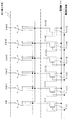
図1をみると、電流源C(i)〜C(i+5)を構成するトランジスタTr(i)〜Tr(i+5)と、切り換え手段と、信号線S(m)〜S(m+5)と、を有する。トランジスタTr(i)〜Tr(i+5)のゲート電極は電流制御線へ接続され、Nチャネル型であるのでソース電極がVssに接続されている。この電流制御線に加える電圧により電流値を制御する。
【0036】
ここでは簡単のため、Tr(i)〜Tr(i+5)のゲート電極には同じ電流制御線が接続されているが、トランジスタごとに電流制御線を設け、電流制御線の電圧を変え、トランジスタごとに電流値を変えてもよい。但しこの場合は、各トランジスタの電流の出力先が切り換わるので、それにあわせて各電流制御線に加える電圧も切り換えておく必要がある。
【0037】
このときトランジスタTr(i)〜Tr(i+5)の特性が揃っていれば電流I(i)〜I(i+5)の値は等しい。しかし実際は、トランジスタTr(i)〜Tr(i+5)の特性のバラツキは大きく、電流I(i)〜I(i+5)の値もばらついてしまう。しかし本発明の切り換え手段により、信号線へ入力される電流I(i)〜I(i+5)を一定期間ごとに選択し切り換えることができる。そのため、発光素子に流れる電流も、一定期間ごとに切り換わることになる。結果として、人間の目には時間的に均一化された発光を見ることとなり輝度むらは減少する。
【0038】
次に図2にアナログスイッチ(またはトランスファーゲイトともいう)を備えた切り換え手段の構成を示す。なお、図2において、図1と同じ部分は同じ符号を用いて示す。トランジスタ線Tr(i)〜Tr(i+5)のドレイン電極は信号線S(m)〜S(m+5)と接続する。ただし、1つの信号線は3つの電流源と接続することができるようになっている。つまりスイッチング機能により3つの電流源のいずれかを選択することができる。
【0039】
例えば、スイッチング機能に端子1を選択する信号が入力されると、信号線S(m+1)は電流源C(i)と接続され、信号線S(m+2)は電流源C(i+1)と接続され、以下同様に信号線と電流源とが接続される。次にスイッチング機能に端子2を選択する信号が入力されると、信号線S(m+1)は電流源C(i+1)と接続され、信号線S(m+2)は電流源C(i+2)と接続され、以下同様に信号線と電流源とが接続される。その次に、スイッチング機能に端子3を選択する信号が入力されると、信号線S(m+1)は電流源C(i+2)と接続され、信号線S(m+2)は電流源C(i+3)と接続され、以下同様に信号線と電流源とが接続される。
【0040】
この接続を上記本発明の接続を一般化するため関数を用いて表すと、i=3であるとき、前記電流源はF1(N)=N+a、F2(N)=N+b、F3(N)=N+c、(但しa、b、cは整数でありかつa≠b≠c)を満たすように設定され、a=−1、b=0、c=1であると表すことができる。
【0041】
上記したように、1つの信号線に3つの電流源からの電流が切り換わることで、表示のバラツキを抑えることができる。
【0042】
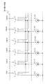
図3には、スイッチング機能を有する切り換え手段にアナログスイッチを用いた具体的な例を説明する。なお、図3において、図2と同じ部分は同じ符号を用いて示しており、電流源C(i)〜C(i+5)はトランジスタTr(i)〜Tr(i+5)を有している。
【0043】
図3に示すA(l)〜A(l+2)、A(l)b〜A(l+2)bは配線であり、複数のアナログスイッチと接続される。これらのアナログスイッチは1つの信号線に接続される群(これを切り換え切り換えユニットという)を形成している。図3をみるとアナログスイッチを3つ有する切り換えユニットU(n)〜U(n+5)は、それぞれ信号線S(m)〜S(m+5)に接続される。この切り換えユニットが複数集まり切り換え手段を構成している。
【0044】
ここで電流源C(i+1)をみると、トランジスタTr(i+1)のドレイン電極は切り換えユニットU(n+1)の1つのアナログスイッチと、切り換えユニットU(n)の1つのアナログスイッチと、切り換えユニットU(n+2)の1つのアナログスイッチと、に接続される。すなわちトランジスタのドレイン電極は3つ切り換え切り換えユニットの1つのアナログスイッチと接続される。同様に電流源C(i)、C(i+2)、C(i+3)、C(i+4)、C(i+5)もそれぞれのアナログスイッチに接続される。
【0045】
そして配線A(l)とA(l)bとに信号が入力されると、接続されるアナログスイッチが選択され導通状態となる。そして、該選択されたアナログスイッチと接続する電流源C(i+1)から信号線S(m+2)へ電流が流れる。同様に各電流源C(i+1)、C(i+3)、C(i+4)、C(i+5)、C(i+6)からそれぞれ信号線S(m)、S(m+2)、S(m+3)、S(m+4)、S(m+5)へ電流が流れる。これを選択(1)と記す。
【0046】
次に配線A(l+1)とA(l+1)bとに信号が入力されると、接続されるアナログスイッチが選択され導通状態となる。そして、該選択されたアナログスイッチと接続する電流源C(i+1)から信号線S(m+1)へ電流が流れる。同様に各電流源C(i+1)、C(i+3)、C(i+4)、C(i+5)、C(i+6)からそれぞれ信号線S(m+1)、S(m+3)、S(m+4)、S(m+5)、S(m+6)へ電流が流れる。また、電流源C(i+6)は記載されないが、電流源C(i+5)の右隣の電流源である。これを選択(2)と記す。
【0047】
次に配線A(l+2)とA(l+2)bとに信号が入力されると、接続されるアナログスイッチが選択され導通状態となる。そして、該選択されたアナログスイッチと接続する電流源C(i+1)から信号線S(m)へ電流が流れる。同様に各電流源C(i+1)、C(i+3)、C(i+4)、C(i+5)、C(i+6)からそれぞれ信号線S(m−1)、S(m+1)、S(m+2)、S(m+3)、S(m+4)へ電流が流れる。また、信号線S(m−1)は記載されないが、信号線S(m)の左隣の信号線である。これを選択(3)と記す。
【0048】
この選択(1)〜選択(3)を一定期間ごとで繰り返すことにより、電流源(i)〜電流源(i+5)から信号線S(m)〜S(m+5)に入力される電流がばらついていても、表示は均一化してみえる。
【0049】
ここで本発明の信号線駆動回路の切り換える期間について、図4のタイミングチャートを示して説明する。図4のF1〜F3はフレーム期間であり、発光装置が1画像を表示する期間を示すものである。なお1フレーム期間は、通常、人間の目がちらつきを感じない様に、1/60秒程度に設定されている。またA(l)〜A(l+2)及びA(l)b〜A(l+2)bは、配線A(l)〜A(l+2)及び配線A(l)b〜A(l+2)bに入力される信号の電位を示す。
【0050】
第1のフレーム期間F1に設けられるA(l)に入力される信号の電位がHigh(H)で、かつA(l)bに入力される信号の電位がLow(L)である切り換え期間では、配線A(l)及びA(l)bに接続されるアナログスイッチが導通状態となり、該導通されたアナログスイッチと接続するトランジスタからの電流が信号線へ入力される。そのため、導通状態となるアナログスイッチは各切り換えユニットに1つだけである。
【0051】
第2のフレーム期間F2に設けられるA(l+1)に入力される信号の電位がHigh(H)で、かつA(l+1)bに入力される信号の電位がLow(L)である切り換え期間では、配線A(l+1)及びA(l+1)bに接続されるアナログスイッチが導通状態となり、該導通されたアナログスイッチと接続するトランジスタからの電流が信号線へ入力される。
【0052】
第3のフレーム期間F3に設けられるA(l+2)に入力される信号の電位がHigh(H)で、かつA(l+2)bに入力される信号の電位がLow(L)である切り換え期間では、配線A(l+2)及びA(l+2)bに接続されるアナログスイッチが導通状態となり、該導通されたアナログスイッチと接続するトランジスタからの電流が信号線へ入力される。
【0053】
このフレーム期間F1〜F3を繰り返すことにより、切り換え手段は信号線S(m)〜S(m+5)に流れる電流を順に切り換えることができる。
【0054】
本実施例では、N型トランジスタを有する電流源に接続される電源線をVssとして、電流が画素からVssへ流れる構成を説明したが、上述したように画素の極性によってトランジスタの極性を設定すればよい。従って、画素へ電流が流れる構成の場合は、電源線をVddとし、電流源のトランジスタをP型の導電型とすればよい。
【0055】
次に、電流源にDA変換機能を持たせた場合について説明する。例えば3ビットのデジタルビデオ信号に対して、8階調のアナログ値を持つ電流を出力する場合で説明する。
【0056】
図5は、上記のような電流源回路の具体的な回路構成を示している。図5に示すように、電流源はそれぞれ3つのトランジスタTr1(i)、Tr2(i)、Tr3(i)を有している。そして3つのトランジスタTr1(i)、Tr2(i)、Tr3(i)のW(ゲート幅)/L(ゲート長)は=1:2:4としておけば、同じゲート電圧が加わっている場合、トランジスタTr1(i)、Tr2(i)、Tr3(i)を流れる電流は1:2:4となる。つまり電流源から供給される電流は1:2:4となり、23=8段階で電流の大きさを制御することができる。そうすると電流源回路は、3ビットのデジタルビデオ信号に対して、8階調のアナログ値を持つ電流を出力することが出来る。
【0057】
なお、トランジスタTr1(i)、Tr2(i)、Tr3(i)のうちのどれがオン状態になり、どれがオフ状態になるかは各ゲートに加える電圧を制御すればよい。それにより、電流源C(i)〜C(i+5)が出力する電流値を制御することができる。ただし、切り換え手段により、電流源C(i)〜C(i+5)の電流がそれぞれ、S(m)〜S(m+5)のどれに入力されるかはかわってくる。従ってそれにあわせて、電流源C(i)〜C(i+5)のトランジスタTr1(i)、Tr2(i)、Tr3(i)に加える電圧も切り換えておく必要がある。
【0058】
このように電流源にDA変換機能を持たせることにより、高精度な階調表示を行うことができる。また、ビット数は実施者が適宜設定すれば良く、そのビット数に応じてトランジスタを設計すればよい。
【0059】
上述した本発明の信号線駆動回路を用いた発光装置では、画素の表示ムラが視覚的に低減された、均一で表示ムラのない表示を提供する発光装置を得ることができる。外付け回路を用いて信号線に入力する場合においても、本発明を外付け回路に適用することにより、均一で表示ムラのない画素を提供することができる。
【0060】
また、信号線駆動回路の半導体素子をポリシリコントランジスタで形成する場合、画素部の半導体素子にポリシリコントランジスタをもちいることができるため、同一基板上に画素部と信号線駆動回路を備えた周辺回路部とを一体形成することができ、小型化・軽量化を達成できる。更に同一基板上に画素部と周辺回路部とを一体形成することにより外付け回路を付ける必要がない。よって、信号線と外付け回路とを接続時の、複雑な工程や不良を省き、信頼性が向上される。
【0061】
(実施例2)
【0062】
なお、本発明の信号線と電流源との接続は、1つの信号線に対して電流源が2つ以上であれば、電流源(電流源の列)の数は非対称であっても、電流源(電流源の列番号)が非対称の位置にあってもよく、信号線へ流れる電流を切り換えることにより、表示が均一化したようにみえる。本実施例では、切り換え手段の切り換えユニットと、信号線と、電流源との接続構成を例示する。
【0063】
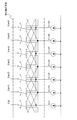
図8には、電流源C(i)〜C(i+5)と信号線S(m)〜S(m+5)とが切り換え手段を介して接続される。この切り換え手段は電流源からの電流を切り換える機能を持っていればよく、図の煩雑さを避けるため、この切り換える機能を模式的に表す3つの端子とスイッチング機能を有する構成で記載する。
【0064】
例えば信号線S(m+2)をみると、電流源C(i+2)、C(i+3)、C(i+4)のいずれかと接続することができる。つまり信号線は最も近い電流源とその右隣2つの電流源とに接続することができる。同様な規則で、信号線S(m)、S(m+1)、S(m+3)、S(m+4)、S(m+5)と信号線とが接続される。
【0065】
この接続を上記本発明の接続を一般化するため関数を用いて表すと、i=3であるとき、前記電流源はF1(N)=N+a、F2(N)=N+b、F3(N)=N+c、(但しa、b、cは整数でありかつa≠b≠c)を満たし、a=−2、b=−1、c=0を満たすと表すことができる。
【0066】
また本発明の電流源と信号線との接続関係は、最も近い位置、すなわち列にある電流源と信号線とを接続する必要はなく、離れた位置にある電流源と信号線と接続する構成でも構わない。その例として、図9に示す接続構成を説明する。
【0067】
図9には、電流源C(i)〜C(i+6)と信号線S(m)〜S(m+6)とが切り換え手段を介して接続される。この切り換え手段も同様に3つの端子とスイッチを有する構成で記載する。
【0068】
例えば信号線S(m+2)をみると、電流源C(i)、C(i+2)、C(i+4)のいずれかと接続することができる。つまり信号線は最も近い電流源とその1つ間をあけた両隣の2本の電流源とに接続することができる。同様な規則で、信号線S(m)、S(m+1)、S(m+3)、S(m+4)、S(m+5)、S(m+6)と電流源とが接続される。
【0069】
この接続を上記本発明の接続を一般化するため関数を用いて表すと、i=3であるとき、前記電流源はF1(N)=N+a、F2(N)=N+b、F3(N)=N+c、(但しa、b、cは整数でありかつa≠b≠c)を満たし、a=−2、b=0、c=−2を満たすと表すことができる。
【0070】
また、本発明の電流源と信号線との接続関係は、信号線が接続する電流源は3つに限るものではない。図10には一つの切り換えユニットにおいて、電流源が5本接続される例を示す。
【0071】
図10には、電流源C(i)〜C(i+6)と信号線S(m)〜S(m+6)とが切り換え手段を介して接続される。この切り換え手段における切り換えユニットも同様に5つの端子とスイッチを有する構成で記載する。
【0072】
例えば信号線S(m+2)をみると、電流源C(i)、C(i+1)、C(i+2)、C(i+3)、C(i+4)のいずれかと接続することができる。つまり信号線は最も近い電流源と両隣の2本ずつの電流源とに接続することができる。同様な規則で、信号線S(m)、S(m+1)、S(m+3)、S(m+4)、S(m+5)と電流源とが接続される。
【0073】
この接続を上記本発明の接続を一般化するため関数を用いて表すと、i=5であるとき、前記電流源はF1(N)=N+a、F2(N)=N+b、F3(N)=N+c、F4(N)=N+d、F5(N)=N+e、(但しa、b、c、d、eは整数でありかつa≠b≠c≠d≠e)を満たし、a=−2、b=−1、c=0、d=1、e=2を満たすと表すことができる。
【0074】
図10のように1つの信号線に対して接続できる電流源が多いほど、表示は均一化してみえ、バラツキを抑えることができる。
【0075】
なお、本実施例は実施例1に記載したアナログスイッチを用いて電流源を切り換える方法とにより、信号線へ流れる電流を切り換えることができる。また、電流源にDA変換機能を持たせた場合も実施例1を参考にすればよい。
【0076】
以上のように、本発明の信号線と電流源との接続は、1つの信号線に対して電流源が2つ以上であれば、非対称の数、非対称の位置にあってもよく、信号線へ流れる電流が切り換わればよい。
【0077】
なお、本実施例は実施例1に記載の切り換え手段と組み合わせて用いることができる。
(実施例3)
【0078】
本実施例では、1フレーム期間(入力されるビデオ信号の同期タイミングに対応する単位フレーム期間内)をサブフレーム期間毎に分割して階調を表示させる(時間階調駆動表示という)場合に、本発明を適応する例を示す。
【0079】
まず時間階調駆動表示について説明する。デジタルのビデオ信号を用いた時間階調の駆動方法(デジタル駆動法)の場合、1フレーム期間中に書き込み期間Taと表示期間(点灯期間ともいう)Tsとが繰り返し出現することで、1つの画像を表示することが可能である。
【0080】
例えばnビットのビデオ信号によって画像を表示する場合、少なくともn個の書き込み期間と、n個の表示期間とが1フレーム期間内に設けられる。n個の書き込み期間と、n個の表示期間は、ビデオ信号の各ビットに対応している。
【0081】
図11(A)に示すように書き込み期間Tam(mは1〜nの任意の数)の次には、同じビット数に対応する表示期間、この場合Tsmが出現する。書き込み期間Taと表示期間Tsとを合わせてサブフレーム期間SFと呼ぶ。mビット目に対応している書き込み期間Tamと表示期間Tsmとを有するサブフレーム期間はSFmとなる。表示期間Ts1〜Tsnの長さは、Ts1:Ts2:…:Tsn=20:21:…:2(n-1)を満たす。
【0082】
各サブフレーム期間において、発光素子を発光させるかさせないかを、デジタルのビデオ信号の各ビットによって選択される。そして、1フレーム期間中における発光する表示期間の長さの和を制御することで、階調数を制御することができる。
【0083】
なお、表示上での画質向上のため、表示期間の長いサブフレーム期間を、幾つかに分割しても良い。具体的な分割の仕方については、特願2000−267164号において開示されているので、参照することができる。
【0084】
本実施例は、このサブフレーム期間の表示期間において、電流源から信号線へ流れる電流を切り換えることが望ましい。書き込み期間で切り換えると、入力された電流、つまり発光素子を発光させるかさせないか上手く情報が伝わらない場合もあるからである。このような短い期間ごとに切り換えることにより、更に発光素子の輝度のバラツキが抑えられ、表示の均一性が向上する。
【0085】
具体的に3ビットの場合を図11(B)に示す。図11(B)をみると1フレーム期間にサブフレーム期間、SF1、SF2、SF3を有し、各サブフレームSF1、SF2、SF3は、書き込み期間Ta1、Ta2、Ta3と表示期間Ts1、Ts2、Ts3有している。そして、電流源を切り換える期間(以下、単に切り換え期間という。)1〜3が表示期間Ts1〜Ts3に設けられている。この切り換え期間1〜3に、信号線に入力される電流を切り換えることによって、短い期間ごとに切り換えることができ、表示がより均一化したように見える。
【0086】
図11(B)では切り換え期間1〜3はいずれも書き込み期間の直前にあるように記載されているが、表示期間の間であれば、どこに切り換え期間を設けても良い。
【0087】
図11(C)にアナログスイッチの入力する信号のタイミングチャートを示す。1フレーム目のSF1ではA1がオン、SF2ではA2がオン、SF3ではA3がオンになっており、2フレーム目のSF1ではA2がオン、SF2ではA3がオン、SF3ではA1がオンとなっている。図11(C)には記載しないが、同様に3フレーム目では、SF1ではA3、SF2ではA1、SF3ではA2がオンとなる。
【0088】
サブフレーム期間SF1からSF3において、A1からA3のオン状態を固定(1フレーム目から3フレーム目の、SF1では全部A1がオン、SF2では全部A2がオン、SF3では全部A3がオン)してしまうと、バラツキの均一化が十分ではなくなる。そのため本実施例のように、サブフレーム期間ごとに切り換えて、かつフレーム期間毎にも切り換えることが望ましい。
【0089】
本実施例は一例であり、どのサブフレーム期間にどの信号を入力するかは適宜設定すればよい。また、具体的な信号の入力方法は図4を参照すればよい。
【0090】
階調表示を高くするために実施例1で説明したDA変換機能を有する電流源とあわせて用いることは好ましく、本実施例は実施例1及び2に記載の発明と組み合わせて用いることができる。
【0091】
(実施例4)
本実施例では、本発明の発光装置の構成について図12を用いて説明する。
【0092】
本発明の発光装置は、基板401上に、複数の画素がマトリクス状に配置された画素部402を有し、画素部402の周辺には、本発明の信号線駆動回路1203、第1の走査線駆動回路404及び第2の走査線駆動回路405を有する。図12(A)においては、信号線駆動回路1203と、2組の走査線駆動回路404、405を有しているが、本発明はこれに限定されず、画素の構成に応じて任意に設計することができる。また信号線駆動回路1203と、第1の走査線駆動回路404及び第2の走査線駆動回路405には、FPC406を介して外部より信号が供給される。
【0093】
第1の走査線駆動回路404及び第2の走査線駆動回路405の構成について図12(B)を用いて説明する。第1の走査線駆動回路404及び第2の走査線駆動回路405は、シフトレジスタ407、バッファ408を有する。動作を簡単に説明すると、シフトレジスタ407は、クロック信号(G-CLK)、スタートパルス(S-SP)及びクロック反転信号(G-CLKb)に従って、順次サンプリングパルスを出力する。その後バッファ408で増幅されたサンプリングパルスは、走査線に入力されて1行ずつ選択状態にしていく。そして選択された走査線によって、制御される画素には、順に信号線から信号電流Idataが書き込まれる。
【0094】
なおシフトレジスタ407と、バッファ408の間にはレベルシフタ回路を配置した構成にしてもよい。レベルシフタ回路を配置することによって、電圧振幅を大きくすることが出来る。
【0095】
信号線駆動回路1203の構成については以下に後述する。また本実施例は、実施例1、2、3と任意に組み合わせることが可能である。
【0096】
また、本発明の信号線駆動回路に設けられる電流源の配置は一直線になっていなくてもよく、信号線駆動回路内でずれて配置されていてもよい。さらに、信号線駆動回路が画素部と対称に2つ設けられていても良い。すなわち本発明は、切り換え手段を介して電流源と信号線と接続されればよく、電流源の配置には限定されない。
【0097】
(実施例5)
本実施例では、図13(A)に示した信号線駆動回路1203の構成とその動作について説明する。本実施例では、1ビットのデジタル階調表示を行う場合に用いる信号線駆動回路1203について図13を用いて説明する。
【0098】
図13(A)には、1ビットのデジタル階調表示を行う場合における信号線駆動回路1203の概略図を示す。信号線駆動回路1203は、シフトレジスタ1211、第1のラッチ回路1212、第2のラッチ回路1213、定電流回路1214を有する。このシフトレジスタ1211、第1のラッチ回路1212、第2のラッチ回路1213は図1で示したビデオ信号用スイッチとして機能する。
【0099】
動作を簡単に説明するとシフトレジスタ1211は、フリップフロップ回路(FF)等を複数列用いて構成され、クロック信号(S-CLK)、スタートパルス(S-SP)、クロック反転信号(S-CLKb)が入力される。これらの信号のタイミングに従って、順次サンプリングパルスが出力される。
【0100】
シフトレジスタ1211より出力されたサンプリングパルスは、第1のラッチ回路1212に入力される。第1のラッチ回路1212には、デジタルビデオ信号が入力されており、サンプリングパルスが入力されるタイミングに従って、各列でビデオ信号を保持していく。
【0101】
第1のラッチ回路1212において、最終列までビデオ信号の保持が完了すると、水平帰線期間中に、第2のラッチ回路1213にラッチパルスが入力され、第1のラッチ回路1212に保持されていたビデオ信号は、一斉に第2のラッチ回路1213に転送される。すると、第2のラッチ回路1213に保持されたビデオ信号は、1行分が同時にビデオ用スイッチへと入力されることになる。このビデオ用スイッチをオン・オフさせることにより、画素への信号を入力するか否かを制御し、階調を表現する。
【0102】
第2のラッチ回路1213に保持されたビデオ信号が定電流回路1214に入力されている間、シフトレジスタ1211においては再びサンプリングパルスが出力される。以後この動作を繰り返し、1フレーム分のビデオ信号の処理を行う。
【0103】
また定電流回路1214は、電流源回路を複数列用いて構成される。図13(B)には、シフトレジスタ1211、第1のラッチ回路1212、第2のラッチ回路1213の具体的な回路を示している。
【0104】
また本実施例は、実施例1、2、3に記載の発明と任意に組み合わせることが可能である。
【0105】
(実施例6)
【0106】
本発明の発光装置を用いた電子機器として、ビデオカメラ、デジタルカメラ、ゴーグル型ディスプレイ(ヘッドマウントディスプレイ)、ナビゲーションシステム、音響再生装置(カーオーディオ、オーディオコンポ等)、ノート型パーソナルコンピュータ、ゲーム機器、携帯情報端末(モバイルコンピュータ、携帯電話、携帯型ゲーム機または電子書籍等)、記録媒体を備えた画像再生装置(具体的にはDigital Versatile Disc(DVD)等の記録媒体を再生し、その画像を表示しうるディスプレイを備えた装置)などが挙げられる。特に、斜め方向から画面を見る機会が多い携帯情報端末は、視野角の広さが重要視されるため、発光装置を用いることが望ましい。それら電子機器の具体例を図15に示す。
【0107】
図15(A)は発光装置であり、筐体2001、支持台2002、表示部2003、スピーカー部2004、ビデオ入力端子2005等を含む。本発明の発光装置は表示部2003に用いることができる。また本発明により、図15(A)に示す発光装置が完成される。発光装置は自発光型であるためバックライトが必要なく、液晶ディスプレイよりも薄い表示部とすることができる。なお、発光装置は、パソコン用、TV放送受信用、広告表示用などの全ての情報表示用発光装置が含まれる。
【0108】
図15(B)はデジタルスチルカメラであり、本体2101、表示部2102、受像部2103、操作キー2104、外部接続ポート2105、シャッター2106等を含む。本発明の発光装置は表示部2102に用いることができる。また本発明により、図15(B)に示すデジタルスチルカメラが完成される。
【0109】
図15(C)はノート型パーソナルコンピュータであり、本体2201、筐体2202、表示部2203、キーボード2204、外部接続ポート2205、ポインティングマウス2206等を含む。本発明の発光装置は表示部2203に用いることができる。また本発明により、図15(C)に示す発光装置が完成される。
【0110】
図15(D)はモバイルコンピュータであり、本体2301、表示部2302、スイッチ2303、操作キー2304、赤外線ポート2305等を含む。本発明の発光装置は表示部2302に用いることができる。また本発明により、図15(D)に示すモバイルコンピュータが完成される。
【0111】
図15(E)は記録媒体を備えた携帯型の画像再生装置(具体的にはDVD再生装置)であり、本体2401、筐体2402、表示部A2403、表示部B2404、記録媒体(DVD等)読み込み部2405、操作キー2406、スピーカー部2407等を含む。表示部A2403は主として画像情報を表示し、表示部B2404は主として文字情報を表示するが、本発明の発光装置はこれら表示部A、B2403、2404に用いることができる。なお、記録媒体を備えた画像再生装置には家庭用ゲーム機器なども含まれる。また本発明により、図15(E)に示すDVD再生装置が完成される。
【0112】
図15(F)はゴーグル型ディスプレイ(ヘッドマウントディスプレイ)であり、本体2501、表示部2502、アーム部2503を含む。本発明の発光装置は表示部2502に用いることができる。また本発明により、図15(F)に示すゴーグル型ディスプレイが完成される。
【0113】
図15(G)はビデオカメラであり、本体2601、表示部2602、筐体2603、外部接続ポート2604、リモコン受信部2605、受像部2606、バッテリー2607、音声入力部2608、操作キー2609等を含む。本発明の発光装置は表示部2602に用いることができる。また本発明により、図15(G)に示すビデオカメラが完成される。
【0114】
ここで図15(H)は携帯電話であり、本体2701、筐体2702、表示部2703、音声入力部2704、音声出力部2705、操作キー2706、外部接続ポート2707、アンテナ2708等を含む。本発明の発光装置は表示部2703に用いることができる。なお、表示部2703は黒色の背景に白色の文字を表示することで携帯電話の消費電流を抑えることができる。また本発明により、図15(H)に示す携帯電話が完成される。
【0115】
なお、将来的に発光材料の発光輝度が高くなれば、出力した画像情報を含む光をレンズ等で拡大投影してフロント型若しくはリア型のプロジェクターに用いることも可能となる。
【0116】
また、上記電子機器はインターネットやCATV(ケーブルテレビ)などの電子通信回線を通じて配信された情報を表示することが多くなり、特に動画情報を表示する機会が増してきている。発光材料の応答速度は非常に高いため、発光装置は動画表示に好ましい。
【0117】
また、発光装置は発光している部分が電力を消費するため、発光部分が極力少なくなるように情報を表示することが望ましい。従って、携帯情報端末、特に携帯電話や音響再生装置のような文字情報を主とする表示部に発光装置を用いる場合には、非発光部分を背景として文字情報を発光部分で形成するように駆動することが望ましい。
【0118】
以上の様に、本発明の適用範囲は極めて広く、あらゆる分野の電子機器に用いることが可能である。また本実施例の電子機器は、実施例1〜実施例5に示したいずれの構成の信号線駆動回路を用いることができる。
【発明の効果】
本発明により、電流源回路におけるトランジスタ特性のバラツキの影響を抑制し、トランジスタの特性に左右されない、半導体集積回路及び半導体集積回路の駆動方法を提供することができる。また、本発明の半導体集積回路を備えた駆動回路部と画素部を備えた発光装置を提供することができる。特に、本発明の半導体集積回路を駆動回路部の信号線駆動回路に適応した、マトリクス状に複数の画素が配置され、各画素にスイッチング素子及び発光素子が配置されたアクティブマトリクス型の発光装置を提供することができる。また、本発明は画素部と駆動回路部との素子をポリシリコン薄膜トランジスタで形成し、画素部と駆動回路部とが同一基板上に一体形成された発光装置を提供することができる。
【0119】
【図面の簡単な説明】
【図1】 本発明の半導体集積回路の構成を示す図。
【図2】 本発明の半導体集積回路の構成を示す図。
【図3】 本発明の半導体集積回路の構成を示す図。
【図4】 本発明の信号線駆動方法のタイミングチャートを示す図。
【図5】 本発明の半導体集積回路の構成を示す図。
【図6】 本発明の半導体集積回路の構成を示す図。
【図7】 本発明の半導体集積回路の切り換え手段の構成を示す図。
【図8】 本発明の半導体集積回路の構成を示す図。
【図9】 本発明の半導体集積回路の構成を示す図。
【図10】 本発明の半導体集積回路の構成を示す図。
【図11】 本発明の信号線駆動方法のタイミングチャートを示す図。
【図12】 本発明の発光装置の構造を示す図。
【図13】 本発明の半導体集積回路の構成を示す図
【図14】 発光装置の画素の回路図。
【図15】 本発明の発光装置が適用される電子機器を示す図。[0001]
BACKGROUND OF THE INVENTION
The present invention relates to a technology of a semiconductor integrated circuit and a driving method thereof. Further, the present invention relates to a light emitting device including a driving circuit portion including a semiconductor integrated circuit of the present invention and a pixel portion. In particular, the present invention relates to an active matrix light-emitting device in which a plurality of pixels are arranged in a matrix and a switching element and a light-emitting element are arranged in each pixel, in which the semiconductor integrated circuit of the present invention is adapted to a signal line driver circuit of a driver circuit portion. .
[0002]
[Prior art]
In recent years, research and development of a light-emitting device using a light-emitting element which is a self-light-emitting element has been advanced as a light-emitting device. These light-emitting devices are widely used as light-emitting devices when using a display screen of a mobile phone or a personal computer, taking advantage of high image quality, thinness, and light weight. In particular, light-emitting devices using light-emitting elements have features such as fast response speed, low voltage, and low power consumption that are suitable for moving image display. A wide range of applications is expected, and it is attracting much attention as a next-generation display.
[0003]
One of the light emitting elements is an organic light emitting diode (OLED) having a structure in which an organic compound layer is sandwiched between an anode, a cathode, and the anode and the cathode. This organic compound layer usually has a laminated structure, and a typical example is a laminated structure of “hole transport layer / light emitting layer / electron transport layer” proposed by Tang et al. Of Kodak Eastman Company.
[0004]
When the light emitting element emits light, the semiconductor element that drives the light emitting element is formed of polysilicon (polycrystalline silicon) having a large on-state current. A polysilicon transistor formed of polysilicon is used as a semiconductor element for driving the light emitting element. The amount of current flowing through the light-emitting element and the luminance of the light-emitting element are in a directly proportional relationship, and the light-emitting element emits light with luminance according to the amount of current flowing through the organic compound layer.
[0005]
By the way, as a driving method for displaying a multi-gradation image on a light emitting device using a light emitting element, an analog gradation method (analog driving method) and a digital gradation method (digital driving method) can be given. The difference between the two systems is in the method of controlling the light emitting element in each of the light emitting and non-light emitting states of the light emitting element. The former analog gradation method is a method of obtaining gradation by controlling the current flowing through the light emitting element in an analog manner. The latter digital gradation method is a method in which the light emitting element is driven only in two states: an on state (a state where the luminance is approximately 100%) and an off state (a state where the luminance is approximately 0%). .
[0006]
Moreover, it can classify | categorize according to the kind of signal input into the light-emitting device using a light emitting element, The electric current input system is proposed as one of them. This current input method is said to be able to control the magnitude of the current flowing through the light emitting element regardless of the characteristics of the TFT driving the light emitting element.
[0007]
As the current input method, both the analog gradation method and the digital gradation method described above are applied. The current input method is a method in which the video signal input to the pixel is a current, and the luminance of the light emitting element is controlled by flowing a current corresponding to the input video signal (current) to the light emitting element.
[0008]
Here, an example of a circuit configuration of a pixel to which a current input method is applied in a light-emitting device and a driving method thereof will be briefly described with reference to FIGS. The pixel illustrated in FIG. 14 includes a
[0009]
The gate electrode of the
[0010]
Next, operations from video signal writing to light emission will be described. First, a pulse is input to the
[0011]
At the moment when the
[0012]
After that, electric charges are gradually accumulated in the
[0013]
In the
[0014]
Subsequently, the light emission operation is started. A pulse is input to the
[0015]
As described above, in the current input method, a drain current having a current value that is the same as or proportional to the signal current set by the
[Problems to be solved by the invention]
[0016]
In a light emitting device to which a current input method is applied, it is necessary to accurately input a signal current corresponding to a video signal to a pixel. However, when a driver circuit (corresponding to the
[0017]
That is, in a light-emitting device to which a current input method is applied, it is necessary to suppress the influence of variation in characteristics of transistors included in a driver circuit that inputs a signal current to a pixel. You In other words, it is necessary to suppress the influence of the characteristic variation of the transistors constituting both the pixel and the drive circuit. That is, since the polysilicon transistor has a large variation, it is difficult to generate an accurate signal current, and the display becomes full of vertical stripes.
[0018]
The present invention has been made in view of the above problems. Therefore, the present invention provides a semiconductor integrated circuit and a method for driving the semiconductor integrated circuit that suppresses the influence of variation in transistor characteristics in each current source of the current source circuit and is not affected by the characteristics of the transistor. In addition, a light-emitting device including a driving circuit portion including a semiconductor integrated circuit of the present invention and a pixel portion is provided. In particular, an active matrix light-emitting device in which a plurality of pixels are arranged in a matrix and a switching element and a light-emitting element are arranged in each pixel, in which the semiconductor integrated circuit of the present invention is adapted to a signal line driver circuit of a driver circuit portion. provide. In addition, the present invention provides a light-emitting device in which elements of a pixel portion and a drive circuit portion are formed of polysilicon thin film transistors, and the pixel portion and the drive circuit portion are integrally formed on the same substrate.
[0019]
Note that the current source circuit includes one or more current sources, and the current source includes one or more transistors. In addition, a current source that supplies a constant current may be called a constant current source.
[0020]
[Means for Solving the Problems]
The semiconductor integrated circuit according to the present invention includes a signal line, a current source circuit that outputs a current input to the signal line, and a means for switching the current source circuit connected to the signal line at regular intervals (hereinafter simply switched). The switching means includes a plurality of circuits having a switching function, and is also referred to as a switching circuit).
[0021]
The switching means of the present invention switches the current source circuit connected to the signal line even if the current output from the current source circuit varies, and accordingly, the current input to the signal line switches at regular intervals. Therefore, the current flowing through the light-emitting element, that is, the luminance appears to be uniform in time, display unevenness can be eliminated, and a light-emitting device that is not affected by variations in transistor characteristics can be provided.
DETAILED DESCRIPTION OF THE INVENTION
(Embodiment)
[0022]
An outline of a signal line driver circuit which is a semiconductor integrated circuit of the present invention will be described with reference to FIG. For the sake of clarity in FIG. 6, the description will be given focusing on the three current sources C (i), C (i + 1), C (i + 2) in the current source circuit and the signal line S (m) for supplying current to the pixel. . The current sources C (i), C (i + 1), C (i + 2) and the signal line S (m) are connected via switching means. By this switching means, the currents I (i) to I (i + 2) supplied from the three current sources C (i) to C (i + 2) are switched at regular intervals and input to the signal line S (m). Features.
[0023]
Next, the switching means will be described. FIG. 7 shows the configuration of the switching means. The current sources C (i), C (i + 1), and C (i + 2) have characteristics that currents I (i), I (i + 1), and I (i + 2) flow, respectively. The current sources C (i), C (i + 1), and C (i + 2) are provided so as to be connected to the signal line S (m) through a switch. A signal is input to the switch, and in response to this signal, the switch has a function of switching so that the signal line S (m) is connected to one of the current sources C (i), C (i + 1), and C (i + 2). Have.
[0024]
When this switch is connected to the current source C (i), a current I (i) flows to the signal line S (m). When the switch is connected to the current source C (i + 1), the current I (i + 1) flows to the signal line S (m). When the switch is connected to the current source C (i + 2), the current I (i + 2) flows to the signal line S (m). That is, I (i), I (i + 1), and I (i + 2) switch and flow through the signal line S (m).
[0025]
The example described with reference to FIGS. 6 and 7 focuses on one signal line for the sake of clarity, but a plurality of actual signal lines are provided as shown in the following embodiments. Although the switch of the switching means in FIG. 7 is described as having a terminal, actually, as shown in the following embodiment, a switching function is provided by a circuit such as an analog switch.
[0026]
In the present invention, since the switching period within this fixed period is very short, even if the characteristics of the current source are different, that is, the current supplied from the current source varies, the display appears uniform to the human eye.
[0027]
Therefore, according to the present invention, a semiconductor integrated circuit including a current source circuit that is not affected by the characteristics of the transistor can be obtained by the switching means as described above. In addition, a light-emitting device that can supply a desired signal current to the light-emitting element and has no display variation is provided.
[0028]
Further, when the present invention is generalized using a function, m signal lines S 1 , S 2 ... S m And i current sources C 1 , C 2 ・ ・ ・ ・ ・ ・ C i A current source circuit having n switching units U 1 , U 2 ... U n The n switching units are connected to j current sources among the i current sources, respectively, and the Mth signal line S is provided. M Is the Nth switching unit U N Connected to the switching unit U N Is the function F k F satisfying (x) (k = 1 to j, x = 1 to n) 1 (N) th current source, F 2 (N) th current source, F Three (N) th current source, F j It is characterized in that it is connected to the (N) th current source.
[0029]
The present invention also provides m signal lines S. 1 , S 2 ... S m And i current sources C 1 , C 2 ・ ・ ・ ・ ・ ・ C i A current source circuit having n switching units U 1 , U 2 ... U n The n switching units are connected to j current sources among the i current sources, respectively, and the Mth signal line S is provided. M Is the Nth switching unit U N Connected to the switching unit U N Is the function F k F satisfying (x) (k = 1 to j, x = 1 to n) 1 (N) th current source, F 2 (N) th current source, F Three (N) th current source, F j The (M-1) th signal line S is connected to the (N) th current source. M-1 Is the (N-1) th switching unit U N-1 Connected to the switching unit U N-1 F satisfying the function 1 (N-1) th current source, F 2 (N-1) th current source, F Three (N-1) th current source, F j It is characterized by being connected to the (N-1) th current source.
[0030]
The present invention can also share a current source between adjacent switching units. When this is expressed using the above function, for example, when i = 3 is satisfied, the current source is F3 (N) = F2 (N + 1) = F1 (N + 2). That is, the current source can be shared by the Nth, N + 1th, and N + 2th switching units adjacent to each other. As another example, when i = 5 is satisfied, the current source is F5 (N) = F4 (N + 1) = F3 (N + 2) = F4 (N + 3) = F5 (N + 4), and the Nth, N + 1 of the adjacent switching units The current source can be shared at the Nth, N + 2, N + 3th, and N + 4th.
[0031]
Thus, since the present invention can share a current source in each switching unit, there is no boundary between a certain signal line and an adjacent signal line, and all signal lines are averaged in the same way. As a result, a boundary is not generated in any part of the display screen, and a light-emitting device free from display streaks and luminance unevenness can be provided.
[0032]
Note that the present invention solves variations in characteristics of elements used in a semiconductor integrated circuit, and even an element other than a polysilicon transistor, for example, a single crystal that is desired to control variation in element characteristics. The same effect can be obtained even with a silicon transistor.
【Example】
Example 1
[0033]
In this embodiment, a structure and a driving method of a current source circuit included in a signal line driver circuit will be specifically described by applying the semiconductor integrated circuit of the present invention to a signal line driver circuit of a driver circuit portion.
[0034]
A specific example of the present invention is shown in FIG. In this embodiment, an example in which the current source is composed of an N-channel transistor will be described. The polarity of the transistor may be either n-channel or p-channel, and is generally determined by the polarity of the pixel. That is, the polarity when the current flows from the pixel to the current source circuit is preferably N-type, and the polarity when the current flows from the current source circuit toward the pixel is preferably P-type. This is because it is more convenient that the source potential of the transistor is fixed.
[0035]
Referring to FIG. 1, transistors Tr (i) to Tr (i + 5) constituting current sources C (i) to C (i + 5), switching means, and signal lines S (m) to S (m + 5) Have. The gate electrodes of the transistors Tr (i) to Tr (i + 5) are connected to the current control line, and since they are N-channel type, the source electrode is connected to Vss. The current value is controlled by the voltage applied to the current control line.
[0036]
Here, for the sake of simplicity, the same current control line is connected to the gate electrodes of Tr (i) to Tr (i + 5). However, a current control line is provided for each transistor, and the voltage of the current control line is changed. The current value may be changed. However, in this case, since the output destination of the current of each transistor is switched, it is necessary to switch the voltage applied to each current control line accordingly.
[0037]
At this time, if the characteristics of the transistors Tr (i) to Tr (i + 5) are uniform, the values of the currents I (i) to I (i + 5) are equal. However, actually, the characteristics of the transistors Tr (i) to Tr (i + 5) vary greatly, and the values of the currents I (i) to I (i + 5) also vary. However, the switching means of the present invention can select and switch the currents I (i) to I (i + 5) input to the signal lines at regular intervals. Therefore, the current flowing through the light emitting element is also switched at regular intervals. As a result, the human eye sees light emission that is uniformed over time, and uneven brightness is reduced.
[0038]
Next, FIG. 2 shows a configuration of switching means provided with an analog switch (also referred to as a transfer gate). 2, the same parts as those in FIG. 1 are denoted by the same reference numerals. The drain electrodes of the transistor lines Tr (i) to Tr (i + 5) are connected to the signal lines S (m) to S (m + 5). However, one signal line can be connected to three current sources. That is, any of the three current sources can be selected by the switching function.
[0039]
For example, when a signal for selecting the
[0040]
Expressing this connection using a function to generalize the connection of the present invention, when i = 3, the current source is F1 (N) = N + a, F2 (N) = N + b, F3 (N) = N + c (where a, b, and c are integers and a ≠ b ≠ c) is set, and can be expressed as a = −1, b = 0, and c = 1.
[0041]
As described above, variations in display can be suppressed by switching the currents from the three current sources to one signal line.
[0042]
FIG. 3 illustrates a specific example in which an analog switch is used as switching means having a switching function. In FIG. 3, the same parts as those in FIG. 2 are denoted by the same reference numerals, and the current sources C (i) to C (i + 5) have transistors Tr (i) to Tr (i + 5).
[0043]
A (l) to A (l + 2) and A (l) b to A (l + 2) b shown in FIG. 3 are wirings and are connected to a plurality of analog switches. These analog switches form a group connected to one signal line (this is called a switching unit). Referring to FIG. 3, switching units U (n) to U (n + 5) having three analog switches are connected to signal lines S (m) to S (m + 5), respectively. A plurality of these switching units constitute a switching means.
[0044]
Looking at the current source C (i + 1), the drain electrode of the transistor Tr (i + 1) is one analog switch of the switching unit U (n + 1), one analog switch of the switching unit U (n), and the switching unit U. And (n + 2) one analog switch. That is, the drain electrode of the transistor is connected to one analog switch of the three switching unit. Similarly, current sources C (i), C (i + 2), C (i + 3), C (i + 4), and C (i + 5) are also connected to the respective analog switches.
[0045]
When a signal is input to the wirings A (l) and A (l) b, the connected analog switch is selected and becomes conductive. Then, a current flows from the current source C (i + 1) connected to the selected analog switch to the signal line S (m + 2). Similarly, signal lines S (m), S (m + 2), S (m + 3), S (from the current sources C (i + 1), C (i + 3), C (i + 4), C (i + 5), and C (i + 6), respectively. m + 4) and current flows to S (m + 5). This is referred to as selection (1).
[0046]
Next, when signals are input to the wirings A (l + 1) and A (l + 1) b, the analog switch to be connected is selected and becomes conductive. Then, a current flows from the current source C (i + 1) connected to the selected analog switch to the signal line S (m + 1). Similarly, signal lines S (m + 1), S (m + 3), S (m + 4), and S (m) from the current sources C (i + 1), C (i + 3), C (i + 4), C (i + 5), and C (i + 6), respectively. m + 5) and current flows to S (m + 6). Further, although the current source C (i + 6) is not described, it is a current source on the right side of the current source C (i + 5). This is referred to as selection (2).
[0047]
Next, when a signal is input to the wirings A (l + 2) and A (l + 2) b, the connected analog switch is selected and becomes conductive. Then, a current flows from the current source C (i + 1) connected to the selected analog switch to the signal line S (m). Similarly, signal lines S (m−1), S (m + 1), S (m + 2), C (i + 1), C (i + 3), C (i + 4), C (i + 5), and C (i + 6) A current flows to S (m + 3) and S (m + 4). Further, the signal line S (m−1) is not described, but is a signal line adjacent to the left of the signal line S (m). This is referred to as selection (3).
[0048]
By repeating this selection (1) to selection (3) at regular intervals, the currents input from the current sources (i) to (i + 5) to the signal lines S (m) to S (m + 5) vary. Even so, the display appears uniform.
[0049]
Here, the switching period of the signal line driver circuit of the present invention will be described with reference to the timing chart of FIG. F1 to F3 in FIG. 4 are frame periods, which indicate periods during which the light emitting device displays one image. Note that one frame period is normally set to about 1/60 seconds so that human eyes do not feel flicker. A (l) to A (l + 2) and A (l) b to A (l + 2) b are input to the wirings A (l) to A (l + 2) and the wirings A (l) b to A (l + 2) b. Signal potential.
[0050]
In the switching period in which the potential of the signal input to A (l) provided in the first frame period F1 is High (H) and the potential of the signal input to A (l) b is Low (L). The analog switches connected to the wirings A (l) and A (l) b are turned on, and a current from a transistor connected to the conducted analog switch is input to the signal line. Therefore, there is only one analog switch that is in a conductive state for each switching unit.
[0051]
In the switching period in which the potential of the signal input to A (l + 1) provided in the second frame period F2 is High (H) and the potential of the signal input to A (l + 1) b is Low (L). The analog switches connected to the wirings A (l + 1) and A (l + 1) b are turned on, and a current from a transistor connected to the conducted analog switch is input to the signal line.
[0052]
In the switching period in which the potential of the signal input to A (l + 2) provided in the third frame period F3 is High (H) and the potential of the signal input to A (l + 2) b is Low (L). The analog switches connected to the wirings A (l + 2) and A (l + 2) b are turned on, and a current from a transistor connected to the conducted analog switch is input to the signal line.
[0053]
By repeating the frame periods F1 to F3, the switching unit can sequentially switch the current flowing through the signal lines S (m) to S (m + 5).
[0054]
In this embodiment, the configuration in which the power line connected to the current source having the N-type transistor is Vss and the current flows from the pixel to Vss has been described. However, as described above, if the polarity of the transistor is set according to the polarity of the pixel Good. Therefore, in the case of a structure in which a current flows to the pixel, the power supply line may be Vdd and the current source transistor may be a P-type conductivity type.
[0055]
Next, the case where the current source has a DA conversion function will be described. For example, a case where a current having an analog value of 8 gradations is output for a 3-bit digital video signal will be described.
[0056]
FIG. 5 shows a specific circuit configuration of the current source circuit as described above. As shown in FIG. 5, each current source has three transistors Tr1 (i), Tr2 (i), and Tr3 (i). If the W (gate width) / L (gate length) of the three transistors Tr1 (i), Tr2 (i), Tr3 (i) is set to 1: 2: 4, the same gate voltage is applied. The current flowing through the transistors Tr1 (i), Tr2 (i), and Tr3 (i) is 1: 2: 4. In other words, the current supplied from the current source is 1: 2: 4. Three = The magnitude of the current can be controlled in 8 steps. Then, the current source circuit can output a current having an analog value of 8 gradations for a 3-bit digital video signal.
[0057]
Note that which of the transistors Tr1 (i), Tr2 (i), and Tr3 (i) is turned on and which is turned off may be controlled by controlling the voltage applied to each gate. Thereby, the current value output from the current sources C (i) to C (i + 5) can be controlled. However, it depends on which of the S (m) to S (m + 5) the currents of the current sources C (i) to C (i + 5) are input by the switching means. Accordingly, the voltages applied to the transistors Tr1 (i), Tr2 (i), and Tr3 (i) of the current sources C (i) to C (i + 5) must be switched accordingly.
[0058]
In this way, by providing the current source with the DA conversion function, it is possible to perform highly accurate gradation display. The number of bits may be set as appropriate by the practitioner, and the transistor may be designed according to the number of bits.
[0059]
In the light-emitting device using the signal line driver circuit of the present invention described above, a light-emitting device that provides a uniform and display-free display in which display unevenness of pixels is visually reduced can be obtained. Even in the case of inputting to a signal line using an external circuit, by applying the present invention to the external circuit, a uniform pixel without display unevenness can be provided.
[0060]
Further, in the case where the semiconductor element of the signal line driver circuit is formed using a polysilicon transistor, a polysilicon transistor can be used for the semiconductor element of the pixel portion. Therefore, the periphery including the pixel portion and the signal line driver circuit on the same substrate. The circuit portion can be integrally formed, and a reduction in size and weight can be achieved. Furthermore, it is not necessary to attach an external circuit by integrally forming the pixel portion and the peripheral circuit portion on the same substrate. Therefore, complicated processes and defects when connecting the signal line and the external circuit are omitted, and the reliability is improved.
[0061]
(Example 2)
[0062]
Note that the connection between the signal line and the current source according to the present invention is such that if there are two or more current sources for one signal line, the number of current sources (current source columns) is asymmetrical. The source (column number of the current source) may be in an asymmetric position, and the display appears to be uniformed by switching the current flowing to the signal line. In the present embodiment, a connection configuration of the switching unit of the switching means, the signal line, and the current source is illustrated.
[0063]
In FIG. 8, current sources C (i) to C (i + 5) and signal lines S (m) to S (m + 5) are connected via switching means. The switching means only needs to have a function of switching the current from the current source. In order to avoid the complexity of the drawing, the switching means is described with a configuration having three terminals schematically showing the switching function and a switching function.
[0064]
For example, the signal line S (m + 2) can be connected to any one of the current sources C (i + 2), C (i + 3), and C (i + 4). That is, the signal line can be connected to the nearest current source and the two current sources on the right side. The signal lines S (m), S (m + 1), S (m + 3), S (m + 4), S (m + 5) and the signal line are connected according to the same rule.
[0065]
Expressing this connection using a function to generalize the connection of the present invention, when i = 3, the current source is F1 (N) = N + a, F2 (N) = N + b, F3 (N) = N + c, where a, b, and c are integers and a ≠ b ≠ c, and a = −2, b = −1, and c = 0 are satisfied.
[0066]
In addition, the connection relationship between the current source and the signal line of the present invention is such that it is not necessary to connect the current source and the signal line in the closest position, that is, in the column, and the current source and the signal line in a remote position are connected. It doesn't matter. As an example, the connection configuration shown in FIG. 9 will be described.
[0067]
In FIG. 9, current sources C (i) to C (i + 6) and signal lines S (m) to S (m + 6) are connected via switching means. This switching means is also described with a configuration having three terminals and a switch.
[0068]
For example, the signal line S (m + 2) can be connected to any one of the current sources C (i), C (i + 2), and C (i + 4). That is, the signal line can be connected to the nearest current source and two adjacent current sources with one between them. The signal lines S (m), S (m + 1), S (m + 3), S (m + 4), S (m + 5), and S (m + 6) are connected to the current source according to the same rule.
[0069]
Expressing this connection using a function to generalize the connection of the present invention, when i = 3, the current source is F1 (N) = N + a, F2 (N) = N + b, F3 (N) = N + c, where a, b, and c are integers and a ≠ b ≠ c, and a = −2, b = 0, and c = −2.
[0070]
The connection relationship between the current source and the signal line of the present invention is not limited to three current sources connected to the signal line. FIG. 10 shows an example in which five current sources are connected in one switching unit.
[0071]
In FIG. 10, current sources C (i) to C (i + 6) and signal lines S (m) to S (m + 6) are connected via switching means. Similarly, the switching unit in this switching means is described as having a configuration having five terminals and a switch.
[0072]
For example, the signal line S (m + 2) can be connected to any one of the current sources C (i), C (i + 1), C (i + 2), C (i + 3), and C (i + 4). That is, the signal line can be connected to the nearest current source and two adjacent current sources. The signal lines S (m), S (m + 1), S (m + 3), S (m + 4), and S (m + 5) are connected to the current source according to the same rule.
[0073]
Expressing this connection using a function to generalize the connection of the present invention, when i = 5, the current source is F1 (N) = N + a, F2 (N) = N + b, F3 (N) = N + c, F4 (N) = N + d, F5 (N) = N + e, where a, b, c, d and e are integers and a ≠ b ≠ c ≠ d ≠ e, and a = −2, It can be expressed that b = −1, c = 0, d = 1, and e = 2.
[0074]
As the number of current sources that can be connected to one signal line increases as shown in FIG. 10, the display appears to be uniform, and variation can be suppressed.
[0075]
In this embodiment, the current flowing to the signal line can be switched by the method of switching the current source using the analog switch described in the first embodiment. Also, the first embodiment may be referred to when the current source has a DA conversion function.
[0076]
As described above, the connection between the signal line and the current source of the present invention may be in an asymmetrical number and an asymmetrical position as long as there are two or more current sources for one signal line. It suffices if the current flowing to the is switched.
[0077]
This embodiment can be used in combination with the switching means described in the first embodiment.
(Example 3)
[0078]
In this embodiment, when one frame period (within a unit frame period corresponding to the synchronization timing of the input video signal) is divided for each subframe period to display gradation (referred to as time gradation drive display), An example to which the present invention is applied is shown.
[0079]
First, time gradation drive display will be described. In the case of a time grayscale driving method (digital driving method) using a digital video signal, a writing period Ta and a display period (also referred to as a lighting period) Ts repeatedly appear in one frame period, so that one image is displayed. Can be displayed.
[0080]
For example, when an image is displayed by an n-bit video signal, at least n writing periods and n display periods are provided in one frame period. The n writing periods and the n display periods correspond to each bit of the video signal.
[0081]
As shown in FIG. 11A, a display period corresponding to the same number of bits, in this case Tsm, appears after the writing period Tam (m is an arbitrary number from 1 to n). The writing period Ta and the display period Ts are collectively referred to as a subframe period SF. The subframe period having the writing period Tam and the display period Tsm corresponding to the m-th bit is SFm. The length of the display periods Ts1 to Tsn is Ts1: Ts2:...: Tsn = 2 0 : 2 1 : ...: 2 (n-1) Meet.
[0082]
Whether or not the light emitting element emits light in each subframe period is selected by each bit of the digital video signal. Then, the number of gradations can be controlled by controlling the sum of the lengths of the display periods during which light is emitted during one frame period.
[0083]
Note that a subframe period having a long display period may be divided into several parts in order to improve image quality on display. A specific method of division is disclosed in Japanese Patent Application No. 2000-267164, and can be referred to.
[0084]
In this embodiment, it is desirable to switch the current flowing from the current source to the signal line in the display period of the subframe period. This is because if the switching is performed during the writing period, the input current, that is, whether or not the light emitting element is caused to emit light may not be transmitted successfully. By switching at such a short period, variation in luminance of the light emitting elements is further suppressed, and display uniformity is improved.
[0085]
Specifically, the case of 3 bits is shown in FIG. Referring to FIG. 11B, one frame period includes subframe periods SF1, SF2, and SF3. Each of the subframes SF1, SF2, and SF3 includes a writing period Ta1, Ta2, and Ta3 and a display period Ts1, Ts2, and Ts3. Have. Then, periods (hereinafter simply referred to as switching periods) 1 to 3 for switching the current source are provided in the display periods Ts1 to Ts3. By switching the current input to the signal line during the
[0086]
In FIG. 11B, the
[0087]
FIG. 11C shows a timing chart of signals input to the analog switch. In the first frame, SF1, A1 is on, in SF2, A2 is on, in SF3, A3 is on, in SF1, A2 is on, in SF2, A3 is on, and in SF3, A1 is on. Yes. Although not shown in FIG. 11C, similarly, in the third frame, A3 is turned on in SF1, A1 is turned on in SF2, and A2 is turned on in SF3.
[0088]
In the subframe periods SF1 to SF3, the ON state of A1 to A3 is fixed (from the first frame to the third frame, all A1 is on in SF1, all A2 is on in SF2, and all A3 is on in SF3). Then, the uniformity of the variation is not sufficient. Therefore, as in the present embodiment, it is desirable to switch every subframe period and also every frame period.
[0089]
This embodiment is an example, and what signal is input in which subframe period may be appropriately set. A specific signal input method may be referred to FIG.
[0090]
In order to increase the gradation display, it is preferably used in combination with the current source having the DA conversion function described in the first embodiment, and this embodiment can be used in combination with the inventions described in the first and second embodiments.
[0091]
Example 4
In this example, the structure of the light-emitting device of the present invention will be described with reference to FIG.
[0092]
A light-emitting device of the present invention includes a
[0093]
The structures of the first scan
[0094]
Note that a level shifter circuit may be provided between the
[0095]
The configuration of the signal line driver circuit 1203 will be described later. This embodiment can be arbitrarily combined with
[0096]
In addition, the arrangement of the current sources provided in the signal line driver circuit of the present invention may not be a straight line, and may be shifted in the signal line driver circuit. Further, two signal line driver circuits may be provided symmetrically with the pixel portion. That is, the present invention is not limited to the arrangement of the current source, as long as it is connected to the current source and the signal line via the switching means.
[0097]
(Example 5)
In this embodiment, a structure and operation of the signal line driver circuit 1203 illustrated in FIG. 13A will be described. In this embodiment, a signal line driver circuit 1203 used in the case of performing 1-bit digital gradation display will be described with reference to FIG.
[0098]
FIG. 13A is a schematic diagram of the signal line driver circuit 1203 in the case of performing 1-bit digital gradation display. The signal line driver circuit 1203 includes a
[0099]
The operation will be briefly described. The
[0100]
The sampling pulse output from the
[0101]
When the
[0102]
While the video signal held in the
[0103]
The constant current circuit 1214 is configured using a plurality of current source circuits. FIG. 13B illustrates specific circuits of the
[0104]
In addition, this embodiment can be arbitrarily combined with the inventions described in
[0105]
(Example 6)
[0106]
As an electronic device using the light emitting device of the present invention, a video camera, a digital camera, a goggle type display (head mounted display), a navigation system, a sound reproduction device (car audio, audio component, etc.), a notebook type personal computer, a game device, Play back a recording medium such as a portable information terminal (mobile computer, mobile phone, portable game machine, electronic book, etc.) or recording medium (specifically, Digital Versatile Disc (DVD)) A device having a display capable of displaying). In particular, it is desirable to use a light-emitting device for a portable information terminal that often has an opportunity to see a screen from an oblique direction because the wide viewing angle is important. Specific examples of these electronic devices are shown in FIGS.
[0107]
FIG. 15A illustrates a light-emitting device, which includes a
[0108]
FIG. 15B illustrates a digital still camera, which includes a
[0109]
FIG. 15C illustrates a laptop personal computer, which includes a
[0110]
FIG. 15D illustrates a mobile computer, which includes a
[0111]
FIG. 15E illustrates a portable image reproducing device (specifically, a DVD reproducing device) provided with a recording medium, which includes a
[0112]
FIG. 15F illustrates a goggle type display (head mounted display), which includes a
[0113]
FIG. 15G shows a video camera, which includes a main body 2601, a
[0114]
Here, FIG. 15H shows a mobile phone, which includes a
[0115]
If the emission luminance of the luminescent material is increased in the future, the light including the output image information can be enlarged and projected by a lens or the like to be used for a front type or rear type projector.
[0116]
In addition, the electronic devices often display information distributed through electronic communication lines such as the Internet and CATV (cable television), and in particular, opportunities to display moving image information are increasing. Since the light emitting material has a very high response speed, the light emitting device is preferable for displaying moving images.
[0117]
In addition, since the light emitting device consumes power in the light emitting portion, it is desirable to display information so that the light emitting portion is minimized. Therefore, when a light emitting device is used for a display unit mainly including character information, such as a portable information terminal, particularly a mobile phone or a sound reproduction device, it is driven so that character information is formed by the light emitting part with the non-light emitting part as the background. It is desirable to do.
[0118]
As described above, the applicable range of the present invention is so wide that it can be used for electronic devices in various fields. Further, the electronic device of this embodiment can use any of the signal line driver circuits shown in
【The invention's effect】
According to the present invention, it is possible to provide a semiconductor integrated circuit and a method for driving the semiconductor integrated circuit, in which the influence of variation in transistor characteristics in the current source circuit is suppressed and the characteristics of the transistors are not affected. In addition, a light-emitting device including a driving circuit portion including a semiconductor integrated circuit of the present invention and a pixel portion can be provided. In particular, an active matrix light-emitting device in which a plurality of pixels are arranged in a matrix and a switching element and a light-emitting element are arranged in each pixel, in which the semiconductor integrated circuit of the present invention is adapted to a signal line driver circuit of a driver circuit portion. Can be provided. In addition, the present invention can provide a light emitting device in which elements of a pixel portion and a drive circuit portion are formed of polysilicon thin film transistors, and the pixel portion and the drive circuit portion are integrally formed on the same substrate.
[0119]
[Brief description of the drawings]
FIG. 1 is a diagram showing a configuration of a semiconductor integrated circuit of the present invention.
FIG. 2 is a diagram showing a configuration of a semiconductor integrated circuit of the present invention.
FIG. 3 is a diagram showing a configuration of a semiconductor integrated circuit of the present invention.
FIG. 4 is a timing chart of a signal line driving method according to the present invention.
FIG. 5 is a diagram showing a configuration of a semiconductor integrated circuit of the present invention.
FIG. 6 is a diagram showing a configuration of a semiconductor integrated circuit of the present invention.
FIG. 7 is a diagram showing a configuration of switching means of a semiconductor integrated circuit according to the present invention.
FIG. 8 is a diagram showing a configuration of a semiconductor integrated circuit of the present invention.
FIG. 9 is a diagram showing a configuration of a semiconductor integrated circuit of the present invention.
FIG. 10 is a diagram showing a configuration of a semiconductor integrated circuit of the present invention.
FIG. 11 is a timing chart of the signal line driving method of the present invention.
FIG. 12 shows a structure of a light emitting device of the present invention.
FIG. 13 is a diagram showing a configuration of a semiconductor integrated circuit according to the present invention.
FIG. 14 is a circuit diagram of a pixel of a light-emitting device.
FIG. 15 is a diagram showing an electronic device to which the light emitting device of the invention is applied.
Claims (27)
i個の電流源C1、C2、・・・、Ciとを有する電流源回路と、
n個の切り換えユニットU1、U2、・・・、Unを含む切り換え手段とを有する半導体集積回路であって、
前記n個の切り換えユニットはそれぞれ前記i個の電流源のうちj個の電流源と電気的に接続され、
前記j個は3個以上であり、
M番目の前記信号線SMはN番目の前記切り換えユニットUNと電気的に接続され、前記切り換えユニットUNは関数Fk(x)(k=1〜j、x=1〜n)を満たすF1(N)番目の電流源、F2(N)番目の電流源、F3(N)番目の電流源、・・・、Fj(N)番目の電流源と電気的に接続され、
(M−1)番目の前記信号線SM-1は(N−1)番目の前記切り換えユニットUN-1と電気的に接続され、前記切り換えユニットUN-1は前記関数を満たすF1(N−1)番目の電流源、F2(N−1)番目の電流源、F3(N−1)番目の電流源、・・・、Fj(N−1)番目の電流源と電気的に接続され、
前記切り換えユニットはそれぞれ前記接続された電流源のうち一つを選択する機能を有し、
前記F1(N)番目の電流源、前記F2(N)番目の電流源、前記F3(N)番目の電流源、・・・、前記Fj(N)番目の電流源のうち少なくとも一つの電流源は、前記F1(N−1)番目の電流源、前記F2(N−1)番目の電流源、前記F3(N−1)番目の電流源、・・・、前記Fj(N−1)番目の電流源のうち少なくとも一つの電流源と同一であり、
前記F1(N)番目の電流源、前記F2(N)番目の電流源、前記F3(N)番目の電流源、・・・、前記Fj(N)番目の電流源のうち少なくとも一つは、前記F1(N−1)番目の電流源、前記F2(N−1)番目の電流源、前記F3(N−1)番目の電流源、・・・、前記Fj(N−1)番目の電流源のいずれとも同一でないことを特徴とする半導体集積回路。m signal lines S 1 , S 2 ,..., S m ,
a current source circuit having i current sources C 1 , C 2 ,..., C i ;
a semiconductor integrated circuit having switching means including n switching units U 1 , U 2 ,...
Each of the n switching units is electrically connected to j current sources of the i current sources;
J is 3 or more,
M-th of the signal lines S M is connected N-th of the switching unit U N and electrically, the switching unit U N is the function F k (x) (k = 1~j, x = 1~n) and F 1 (N) th current source, F 2 (N) th current source, F 3 (N) th current source,..., F j (N) th current source satisfying ,
(M-1) -th said signal lines S M-1 of is electrically connected to the switching unit U N-1 of th (N-1), F 1 the switching unit U N-1 is to satisfy the function (N-1) th current sources, F 2 (N-1) th current sources, F 3 (N-1) th current sources, ···, F j (N- 1) th current source and Electrically connected,
Each of the switching units has a function of selecting one of the connected current sources,
At least one of the F 1 (N) th current source, the F 2 (N) th current source, the F 3 (N) th current source,..., The F j (N) th current source. One current source includes the F 1 (N−1) th current source, the F 2 (N−1) th current source, the F 3 (N−1) th current source,. The same as at least one of the F j (N−1) th current sources;
At least one of the F 1 (N) th current source, the F 2 (N) th current source, the F 3 (N) th current source,..., The F j (N) th current source. One is the F 1 (N−1) th current source, the F 2 (N−1) th current source, the F 3 (N−1) th current source ,. (N-1) A semiconductor integrated circuit which is not the same as any of the current sources.
i個の電流源C1、C2、・・・、Ciとを有する電流源回路と、
n個の切り換えユニットU1、U2、・・・、Unを含む切り換え手段とを有する半導体集積回路であって、
前記n個の切り換えユニットはそれぞれ前記i個の電流源のうちj個の電流源と電気的に接続され、
前記j個は3個以上であり、
M番目の前記信号線SMはN番目の前記切り換えユニットUNと電気的に接続され、前記切り換えユニットUNは関数Fk(x)(k=1〜j、x=1〜n)を満たすF1(N)番目の電流源、F2(N)番目の電流源、F3(N)番目の電流源、・・・、Fj(N)番目の電流源と電気的に接続され、
(M−h)番目の前記信号線SM−hは(N−h)番目の前記切り換えユニットUN−hと電気的に接続され、前記切り換えユニットUN−hは前記関数を満たすF1(N−h)番目の電流源、F2(N−h)番目の電流源、F3(N−h)番目の電流源、・・・、Fj(N−h)番目の電流源と電気的に接続され、
前記切り換えユニットはそれぞれ前記接続された電流源のうち一つを選択する機能を有し、
前記F1(N)番目の電流源、前記F2(N)番目の電流源、前記F3(N)番目の電流源、・・・、前記Fj(N)番目の電流源のうち少なくとも一つの電流源は、前記F1(N−h)番目の電流源、前記F2(N−h)番目の電流源、前記F3(N−h)番目の電流源、・・・、前記Fj(N−h)番目の電流源のうち少なくとも一つの電流源と同一であり、
前記F1(N)番目の電流源、前記F2(N)番目の電流源、前記F3(N)番目の電流源、・・・、前記Fj(N)番目の電流源のうち少なくとも一つは、前記F1(N−h)番目の電流源、前記F2(N−h)番目の電流源、前記F3(N−h)番目の電流源、・・・、前記Fj(N−h)番目の電流源のいずれとも同一でないことを特徴とする半導体集積回路。m signal lines S 1 , S 2 ,..., S m ,
a current source circuit having i current sources C 1 , C 2 ,..., C i ;
a semiconductor integrated circuit having switching means including n switching units U 1 , U 2 ,...
Each of the n switching units is electrically connected to j current sources of the i current sources;
J is 3 or more,
M-th of the signal lines S M is connected N-th of the switching unit U N and electrically, the switching unit U N is the function F k (x) (k = 1~j, x = 1~n) and F 1 (N) th current source, F 2 (N) th current source, F 3 (N) th current source,..., F j (N) th current source satisfying ,
(M-h) -th signal line S M-h is electrically connected to the (N-h) -th switching unit U N-h, F 1 the switching unit U N-h is satisfying the function (N-h) -th current source, F 2 (N-h) th current sources, F 3 (N-h) -th current source, ..., and F j (N-h) -th current source Electrically connected,
Each of the switching units has a function of selecting one of the connected current sources,
At least one of the F 1 (N) th current source, the F 2 (N) th current source, the F 3 (N) th current source,..., The F j (N) th current source. One current source includes the F 1 (N−h) th current source, the F 2 (N−h) th current source, the F 3 (N−h) th current source,. Is identical to at least one of the F j (N−h) th current sources,
At least one of the F 1 (N) th current source, the F 2 (N) th current source, the F 3 (N) th current source,..., The F j (N) th current source. One is the F 1 (N−h) th current source, the F 2 (N−h) th current source, the F 3 (N−h) th current source ,. A semiconductor integrated circuit which is not the same as any of the (N-h) th current sources.
第1乃至第3の電流源とを有する電流源回路と、
第1乃至第3の切り換えユニットを含む切り換え手段とを有する半導体集積回路であって、
前記第1の信号線は前記第1の切り換えユニットに電気的に接続され、前記第2の信号線は前記第2の切り換えユニットに電気的に接続され、前記第3の信号線は前記第3の切り換えユニットに電気的に接続され、
前記第1の切り換えユニットは、前記第1及び第2の電流源それぞれと電気的に接続され、
前記第2の切り換えユニットは、前記第1乃至第3の電流源それぞれと電気的に接続され、
前記第3の切り換えユニットは、前記第2及び第3の電流源それぞれと電気的に接続され、
前記第1乃至第3の切り換えユニットはそれぞれ前記接続された電流源のうち一つを選択する機能を有することを特徴とする半導体集積回路。First to third signal lines;
A current source circuit having first to third current sources;
A semiconductor integrated circuit having switching means including first to third switching units,
The first signal line is electrically connected to the first switching unit, the second signal line is electrically connected to the second switching unit, and the third signal line is the third switching unit. Electrically connected to the switching unit
The first switching unit is electrically connected to each of the first and second current sources;
The second switching unit is electrically connected to each of the first to third current sources,
The third switching unit is electrically connected to each of the second and third current sources;
Each of the first to third switching units has a function of selecting one of the connected current sources.
第1乃至第5の電流源とを有する電流源回路と、
第1乃至第3の切り換えユニットを含む切り換え手段とを有する半導体集積回路であって、
前記第1の信号線は前記第1の切り換えユニットに電気的に接続され、前記第2の信号線は前記第2の切り換えユニットに電気的に接続され、前記第3の信号線は前記第3の切り換えユニットに電気的に接続され、
前記第1の切り換えユニットは、前記第1乃至第4の電流源それぞれと電気的に接続され、
前記第2の切り換えユニットは、前記第1乃至第5の電流源それぞれと電気的に接続され、
前記第3の切り換えユニットは、前記第2乃至第5の電流源それぞれと電気的に接続され、
前記第1乃至第3の切り換えユニットはそれぞれ前記接続された電流源のうち一つを選択する機能を有することを特徴とする半導体集積回路。First to third signal lines;
A current source circuit having first to fifth current sources;
A semiconductor integrated circuit having switching means including first to third switching units,
The first signal line is electrically connected to the first switching unit, the second signal line is electrically connected to the second switching unit, and the third signal line is the third switching unit. Electrically connected to the switching unit
The first switching unit is electrically connected to each of the first to fourth current sources,
The second switching unit is electrically connected to each of the first to fifth current sources,
The third switching unit is electrically connected to each of the second to fifth current sources,
Each of the first to third switching units has a function of selecting one of the connected current sources.
前記単位フレーム期間はm(mは2以上の自然数)個のサブフレーム期間SF1、SF2、・・・、SFmを有し、前記m個のサブフレーム期間SF1、SF2、・・・、SFmは、それぞれ書き込み期間Ta1、Ta2、・・・、Tamと表示期間Ts1、Ts2、・・・、Tsmとを有し、
前記表示期間内に前記第1乃至第3の切り換えユニットにより前記電流源のいずれかが選択されることを特徴とする半導体集積回路。In claim 11,
The unit frame period includes m (m is a natural number of 2 or more) subframe periods SF1, SF2,..., SFm, and the m subframe periods SF1, SF2,. Each has writing periods Ta1, Ta2,..., Tam and display periods Ts1, Ts2,.
One of the current sources is selected by the first to third switching units within the display period.
i個の電流源C1、C2、・・・、Ciとを有する電流源回路と、
n個の切り換えユニットU1、U2、・・・、Unを含む切り換え手段とを有し、
前記n個の切り換えユニットはそれぞれ前記i個の電流源のうちj個の電流源と電気的に接続され、
前記j個は3個以上であり、
M番目の前記信号線SMはN番目の前記切り換えユニットUNと電気的に接続され、前記切り換えユニットUNは関数Fk(x)(k=1〜j、x=1〜n)を満たすF1(N)番目の電流源、F2(N)番目の電流源、F3(N)番目の電流源、・・・、Fj(N)番目の電流源と電気的に接続され、
(M−h)番目の前記信号線SM−hは(N−h)番目の前記切り換えユニットUN−hと電気的に接続され、前記切り換えユニットUN−hは前記関数を満たすF1(N−h)番目の電流源、F2(N−h)番目の電流源、F3(N−h)番目の電流源、・・・、Fj(N−h)番目の電流源と電気的に接続され、
前記F1(N)番目の電流源、前記F2(N)番目の電流源、前記F3(N)番目の電流源、・・・、前記Fj(N)番目の電流源のうち少なくとも一つの電流源は、前記F1(N−h)番目の電流源、前記F2(N−h)番目の電流源、前記F3(N−h)番目の電流源、・・・、前記Fj(N−h)番目の電流源のうち少なくとも一つの電流源と同一であり、
前記F1(N)番目の電流源、前記F2(N)番目の電流源、前記F3(N)番目の電流源、・・・、前記Fj(N)番目の電流源のうち少なくとも一つは、前記F1(N−h)番目の電流源、前記F2(N−h)番目の電流源、前記F3(N−h)番目の電流源、・・・、前記Fj(N−h)番目の電流源のいずれとも同一でない半導体集積回路の駆動方法であって、
前記切り換えユニットは一定期間毎に、前記接続される電流源の選択を切り換えることを特徴とする半導体集積回路の駆動方法。m signal lines S 1 , S 2 ,..., S m ,
a current source circuit having i current sources C 1 , C 2 ,..., C i ;
switching means including n switching units U 1 , U 2 ,..., U n ,
Each of the n switching units is electrically connected to j current sources of the i current sources;
J is 3 or more,
M-th of the signal lines S M is connected N-th of the switching unit U N and electrically, the switching unit U N is the function F k (x) (k = 1~j, x = 1~n) and F 1 (N) th current source, F 2 (N) th current source, F 3 (N) th current source,..., F j (N) th current source satisfying ,
(M-h) -th signal line S M-h is electrically connected to the (N-h) -th switching unit U N-h, F 1 the switching unit U N-h is satisfying the function (N-h) -th current source, F 2 (N-h) th current sources, F 3 (N-h) -th current source, ..., and F j (N-h) -th current source Electrically connected,
At least one of the F 1 (N) th current source, the F 2 (N) th current source, the F 3 (N) th current source,..., The F j (N) th current source. One current source includes the F 1 (N−h) th current source, the F 2 (N−h) th current source, the F 3 (N−h) th current source,. Is identical to at least one of the F j (N−h) th current sources,
At least one of the F 1 (N) th current source, the F 2 (N) th current source, the F 3 (N) th current source,..., The F j (N) th current source. One is the F 1 (N−h) th current source, the F 2 (N−h) th current source, the F 3 (N−h) th current source ,. A method of driving a semiconductor integrated circuit that is not identical to any of the (Nh) th current sources,
The method for driving a semiconductor integrated circuit, wherein the switching unit switches selection of the connected current source at regular intervals.
i個の電流源C1、C2、・・・、Ciとを有する電流源回路と、
n個の切り換えユニットU1、U2、・・・、Unを含む切り換え手段と、
シフトレジスタと、前記シフトレジスタより制御される第1のラッチ回路と、前記第1のラッチ回路に保持された信号が転送される第2のラッチ回路と、を有し、
前記n個の切り換えユニットはそれぞれ前記i個の電流源のうちj個の電流源と電気的に接続され、
前記j個は3個以上であり、
M番目の前記信号線SMはN番目の前記切り換えユニットUNと電気的に接続され、前記切り換えユニットUNは関数Fk(x)(k=1〜j、x=1〜n)を満たすF1(N)番目の電流源、F2(N)番目の電流源、F3(N)番目の電流源、・・・、Fj(N)番目の電流源と電気的に接続され、
(M−h)番目の前記信号線SM−hは(N−h)番目の前記切り換えユニットUN−hと電気的に接続され、前記切り換えユニットUN−hは前記関数を満たすF1(N−h)番目の電流源、F2(N−h)番目の電流源、F3(N−h)番目の電流源、・・・、Fj(N−h)番目の電流源と電気的に接続され、
前記F1(N)番目の電流源、前記F2(N)番目の電流源、前記F3(N)番目の電流源、・・・、前記Fj(N)番目の電流源のうち少なくとも一つの電流源は、前記F1(N−h)番目の電流源、前記F2(N−h)番目の電流源、前記F3(N−h)番目の電流源、・・・、前記Fj(N−h)番目の電流源のうち少なくとも一つの電流源と同一であり、
前記F1(N)番目の電流源、前記F2(N)番目の電流源、前記F3(N)番目の電流源、・・・、前記Fj(N)番目の電流源のうち少なくとも一つは、前記F1(N−h)番目の電流源、前記F2(N−h)番目の電流源、前記F3(N−h)番目の電流源、・・・、前記Fj(N−h)番目の電流源のいずれとも同一でない半導体集積回路の駆動方法であって、
前記切り換えユニットは一定期間毎に、前記第2のラッチ回路により制御される前記電流源と前記信号線との電気的な接続を切り換えることを特徴とする半導体集積回路の駆動方法。m signal lines S 1 , S 2 ,..., S m ,
a current source circuit having i current sources C 1 , C 2 ,..., C i ;
switching means including n switching units U 1 , U 2 ,..., U n ;
A shift register, a first latch circuit controlled by the shift register, and a second latch circuit to which a signal held in the first latch circuit is transferred,
Each of the n switching units is electrically connected to j current sources of the i current sources;
J is 3 or more,
M-th of the signal lines S M is connected N-th of the switching unit U N and electrically, the switching unit U N is the function F k (x) (k = 1~j, x = 1~n) and F 1 (N) th current source, F 2 (N) th current source, F 3 (N) th current source,..., F j (N) th current source satisfying ,
(M-h) -th signal line S M-h is electrically connected to the (N-h) -th switching unit U N-h, F 1 the switching unit U N-h is satisfying the function (N-h) -th current source, F 2 (N-h) th current sources, F 3 (N-h) -th current source, ..., and F j (N-h) -th current source Electrically connected,
At least one of the F 1 (N) th current source, the F 2 (N) th current source, the F 3 (N) th current source,..., The F j (N) th current source. One current source includes the F 1 (N−h) th current source, the F 2 (N−h) th current source, the F 3 (N−h) th current source,. Is identical to at least one of the F j (N−h) th current sources,
At least one of the F 1 (N) th current source, the F 2 (N) th current source, the F 3 (N) th current source,..., The F j (N) th current source. One is the F 1 (N−h) th current source, the F 2 (N−h) th current source, the F 3 (N−h) th current source ,. A method of driving a semiconductor integrated circuit that is not identical to any of the (Nh) th current sources,
The method for driving a semiconductor integrated circuit, wherein the switching unit switches an electrical connection between the current source controlled by the second latch circuit and the signal line at regular intervals.
第1乃至第3の電流源とを有する電流源回路と、
第1乃至第3の切り換えユニットを含む切り換え手段とを有し、
前記第1の信号線は前記第1の切り換えユニットに電気的に接続され、前記第2の信号線は前記第2の切り換えユニットに電気的に接続され、前記第3の信号線は前記第3の切り換えユニットに電気的に接続され、
前記第1の切り換えユニットは、前記第1及び第2の電流源それぞれと電気的に接続され、
前記第2の切り換えユニットは、前記第1乃至第3の電流源それぞれと電気的に接続され、
前記第3の切り換えユニットは、前記第2及び第3の電流源それぞれと電気的に接続される半導体集積回路の駆動方法であって、
前記第1乃至第3の切り換えユニットは一定期間毎に、それぞれ前記接続される電流源の選択を切り換えることを特徴とする半導体集積回路の駆動方法。First to third signal lines;
A current source circuit having first to third current sources;
Switching means including first to third switching units,
The first signal line is electrically connected to the first switching unit, the second signal line is electrically connected to the second switching unit, and the third signal line is the third switching unit. Electrically connected to the switching unit
The first switching unit is electrically connected to each of the first and second current sources;
The second switching unit is electrically connected to each of the first to third current sources,
The third switching unit is a method of driving a semiconductor integrated circuit electrically connected to each of the second and third current sources,
The method for driving a semiconductor integrated circuit, wherein the first to third switching units switch selection of the connected current sources at regular intervals.
第1乃至第5の電流源とを有する電流源回路と、
第1乃至第3の切り換えユニットを含む切り換え手段とを有し、
前記第1の信号線は前記第1の切り換えユニットに電気的に接続され、前記第2の信号線は前記第2の切り換えユニットに電気的に接続され、前記第3の信号線は前記第3の切り換えユニットに電気的に接続され、
前記第1の切り換えユニットは、前記第1乃至第4の電流源それぞれと電気的に接続され、
前記第2の切り換えユニットは、前記第1乃至第5の電流源それぞれと電気的に接続され、
前記第3の切り換えユニットは、前記第2乃至第5の電流源それぞれと電気的に接続される半導体集積回路の駆動方法であって、
前記第1乃至第3の切り換えユニットは一定期間毎に、それぞれ前記接続される電流源の選択を切り換えることを特徴とする半導体集積回路の駆動方法。First to third signal lines;
A current source circuit having first to fifth current sources;
Switching means including first to third switching units,
The first signal line is electrically connected to the first switching unit, the second signal line is electrically connected to the second switching unit, and the third signal line is the third switching unit. Electrically connected to the switching unit
The first switching unit is electrically connected to each of the first to fourth current sources,
The second switching unit is electrically connected to each of the first to fifth current sources,
The third switching unit is a method of driving a semiconductor integrated circuit electrically connected to each of the second to fifth current sources,
The method for driving a semiconductor integrated circuit, wherein the first to third switching units switch selection of the connected current sources at regular intervals.
前記単位フレーム期間はm(mは2以上の自然数)個のサブフレーム期間SF1、SF2、・・・、SFmを有し、前記m個のサブフレーム期間SF1、SF2、…SFmは、それぞれ書き込み期間Ta1、Ta2、・・・、Tamと表示期間Ts1、Ts2、・・・、Tsmとを有し、
前記表示期間内に前記一定期間が設けられたことを特徴とする半導体集積回路の駆動方法。In claim 24,
The unit frame period has m (m is a natural number of 2 or more) subframe periods SF1, SF2,..., SFm, and the m subframe periods SF1, SF2,. Ta, Ta2, ..., Tam and display periods Ts1, Ts2, ..., Tsm,
A method for driving a semiconductor integrated circuit, wherein the predetermined period is provided within the display period.
Priority Applications (8)
| Application Number | Priority Date | Filing Date | Title |
|---|---|---|---|
| JP2002059903A JP3923341B2 (en) | 2002-03-06 | 2002-03-06 | Semiconductor integrated circuit and driving method thereof |
| CN031199380A CN1443002B (en) | 2002-03-06 | 2003-03-06 | Semi conductor integrated circuit and its driving method |
| US10/382,467 US7728653B2 (en) | 2002-03-06 | 2003-03-06 | Display and method of driving the same |
| TW092104826A TWI299578B (en) | 2002-03-06 | 2003-03-06 | Semiconductor intergrated circuit and method of driving the same |
| TW095129688A TWI300628B (en) | 2002-03-06 | 2003-03-06 | Semiconductor intergrated circuit and method of driving the same |
| CN201210294941.1A CN102831858B (en) | 2002-03-06 | 2003-03-06 | Semiconductor integrated circuit and method for driving the same |
| US12/791,533 US8004513B2 (en) | 2002-03-06 | 2010-06-01 | Semiconductor integrated circuit and method of driving the same |
| US13/214,288 US8373694B2 (en) | 2002-03-06 | 2011-08-22 | Semiconductor integrated circuit and method of driving the same |
Applications Claiming Priority (1)
| Application Number | Priority Date | Filing Date | Title |
|---|---|---|---|
| JP2002059903A JP3923341B2 (en) | 2002-03-06 | 2002-03-06 | Semiconductor integrated circuit and driving method thereof |
Related Child Applications (1)
| Application Number | Title | Priority Date | Filing Date |
|---|---|---|---|
| JP2006291985A Division JP4658016B2 (en) | 2006-10-27 | 2006-10-27 | Semiconductor device |
Publications (3)
| Publication Number | Publication Date |
|---|---|
| JP2003255880A JP2003255880A (en) | 2003-09-10 |
| JP2003255880A5 JP2003255880A5 (en) | 2005-07-07 |
| JP3923341B2 true JP3923341B2 (en) | 2007-05-30 |
Family
ID=27800159
Family Applications (1)
| Application Number | Title | Priority Date | Filing Date |
|---|---|---|---|
| JP2002059903A Expired - Fee Related JP3923341B2 (en) | 2002-03-06 | 2002-03-06 | Semiconductor integrated circuit and driving method thereof |
Country Status (4)
| Country | Link |
|---|---|
| US (3) | US7728653B2 (en) |
| JP (1) | JP3923341B2 (en) |
| CN (2) | CN1443002B (en) |
| TW (2) | TWI300628B (en) |
Cited By (1)
| Publication number | Priority date | Publication date | Assignee | Title |
|---|---|---|---|---|
| KR20150117749A (en) * | 2014-04-10 | 2015-10-21 | 삼성디스플레이 주식회사 | Organic light emitting display device, and method of driving the same |
Families Citing this family (17)
| Publication number | Priority date | Publication date | Assignee | Title |
|---|---|---|---|---|
| JP3923341B2 (en) * | 2002-03-06 | 2007-05-30 | 株式会社半導体エネルギー研究所 | Semiconductor integrated circuit and driving method thereof |
| WO2004054114A1 (en) | 2002-12-10 | 2004-06-24 | Semiconductor Energy Laboratory Co., Ltd. | Semiconductor device, digital-analog conversion circuit, and display device using them |
| US7961160B2 (en) | 2003-07-31 | 2011-06-14 | Semiconductor Energy Laboratory Co., Ltd. | Display device, a driving method of a display device, and a semiconductor integrated circuit incorporated in a display device |
| US7791570B2 (en) * | 2004-03-12 | 2010-09-07 | Koninklijke Philips Electronics N.V. | Electrical circuit arrangement for a display device |
| CN1934609A (en) * | 2004-03-24 | 2007-03-21 | 罗姆股份有限公司 | Organic el display driving circuit and organic el display device using the same |
| JP2006091850A (en) * | 2004-07-22 | 2006-04-06 | Toshiba Matsushita Display Technology Co Ltd | El display device and inspecting apparatus of el display panel |
| KR100707634B1 (en) | 2005-04-28 | 2007-04-12 | 한양대학교 산학협력단 | Data Driving Circuit and Driving Method of Light Emitting Display Using the same |
| KR100662985B1 (en) * | 2005-10-25 | 2006-12-28 | 삼성에스디아이 주식회사 | Data driving circuit and driving method of organic light emitting display using the same |
| JP3848358B1 (en) * | 2006-02-15 | 2006-11-22 | 株式会社日出ハイテック | Multi-channel drive circuit |
| US8405596B2 (en) * | 2007-01-31 | 2013-03-26 | Sharp Kabushiki Kaisha | Display device having dual scanning signal line driver circuits |
| JP5381823B2 (en) * | 2010-03-10 | 2014-01-08 | カシオ計算機株式会社 | Pixel driving device, light emitting device, electronic device, and driving control method for light emitting device |
| JP2012256012A (en) | 2010-09-15 | 2012-12-27 | Semiconductor Energy Lab Co Ltd | Display device |
| US9781800B2 (en) | 2015-05-21 | 2017-10-03 | Infineon Technologies Ag | Driving several light sources |
| US9974130B2 (en) | 2015-05-21 | 2018-05-15 | Infineon Technologies Ag | Driving several light sources |
| US9918367B1 (en) | 2016-11-18 | 2018-03-13 | Infineon Technologies Ag | Current source regulation |
| US20210041904A1 (en) * | 2019-03-22 | 2021-02-11 | Sitronix Technology Corp. | Current source circuit |
| KR20210013388A (en) | 2019-07-24 | 2021-02-04 | 삼성전자주식회사 | Image sensor |
Family Cites Families (89)
| Publication number | Priority date | Publication date | Assignee | Title |
|---|---|---|---|---|
| US3696393A (en) * | 1971-05-10 | 1972-10-03 | Hughes Aircraft Co | Analog display using light emitting diodes |
| JPS62232827A (en) | 1986-03-31 | 1987-10-13 | 松下電器産業株式会社 | Operation panel driver with lighting device |
| JPH0736410B2 (en) | 1986-12-26 | 1995-04-19 | 古河電気工業株式会社 | Tape-shaped lead for electrical connection |
| JPS6442099A (en) | 1987-08-07 | 1989-02-14 | Sharp Kk | Semiconductor device |
| JP3026439B2 (en) | 1989-01-19 | 2000-03-27 | 株式会社東芝 | Liquid crystal display drive |
| JPH0542488A (en) | 1990-09-04 | 1993-02-23 | Masahisa Miura | Rotary stapler |
| JP3242941B2 (en) | 1991-04-30 | 2001-12-25 | 富士ゼロックス株式会社 | Active EL matrix and driving method thereof |
| JP2544415Y2 (en) | 1991-11-08 | 1997-08-20 | 株式会社ノダ | Floor material |
| JP3390214B2 (en) | 1993-07-19 | 2003-03-24 | パイオニア株式会社 | Display device drive circuit |
| US5594463A (en) * | 1993-07-19 | 1997-01-14 | Pioneer Electronic Corporation | Driving circuit for display apparatus, and method of driving display apparatus |
| SG54123A1 (en) * | 1993-12-22 | 1998-11-16 | Seiko Epson Corp | Liquid-crystal display system and power supply method |
| US5657040A (en) * | 1993-12-29 | 1997-08-12 | Casio Computer Co., Ltd. | Driving apparatus for stably driving high-definition and large screen liquid crystal display panels |
| TW280037B (en) * | 1994-04-22 | 1996-07-01 | Handotai Energy Kenkyusho Kk | Drive circuit of active matrix type display device and manufacturing method |
| JPH09134149A (en) | 1995-11-09 | 1997-05-20 | Seiko Epson Corp | Picture display device |
| EP0718816B1 (en) | 1994-12-20 | 2003-08-06 | Seiko Epson Corporation | Image display device |
| US5805123A (en) * | 1995-03-16 | 1998-09-08 | Texas Instruments Incorporated | Display panel driving circuit having an integrated circuit portion and a high power portion attached to the integrated circuit |
| JPH0981087A (en) | 1995-09-18 | 1997-03-28 | Toshiba Corp | Liquid crystal display device |
| JPH09101759A (en) * | 1995-10-04 | 1997-04-15 | Pioneer Electron Corp | Method and device for driving light emitting element |
| US5719589A (en) * | 1996-01-11 | 1998-02-17 | Motorola, Inc. | Organic light emitting diode array drive apparatus |
| JP3352876B2 (en) | 1996-03-11 | 2002-12-03 | 株式会社東芝 | Output circuit and liquid crystal display driving circuit including the same |
| JP3547561B2 (en) * | 1996-05-15 | 2004-07-28 | パイオニア株式会社 | Display device |
| JPH1083166A (en) | 1996-09-09 | 1998-03-31 | Matsushita Electron Corp | Drive circuit of liquid crystal display device and its control method |
| US5990629A (en) * | 1997-01-28 | 1999-11-23 | Casio Computer Co., Ltd. | Electroluminescent display device and a driving method thereof |
| US6229506B1 (en) * | 1997-04-23 | 2001-05-08 | Sarnoff Corporation | Active matrix light emitting diode pixel structure and concomitant method |
| JP3102411B2 (en) | 1997-05-29 | 2000-10-23 | 日本電気株式会社 | Driving circuit for organic thin film EL device |
| TW381249B (en) * | 1997-05-29 | 2000-02-01 | Nippon Electric Co | Driving circuits of organic thin film electric laser components |
| JP3375117B2 (en) * | 1997-06-11 | 2003-02-10 | シャープ株式会社 | Semiconductor device, manufacturing method thereof, and liquid crystal display device |
| JP3287391B2 (en) * | 1997-07-17 | 2002-06-04 | シャープ株式会社 | Semiconductor device |
| JPH11183870A (en) | 1997-12-18 | 1999-07-09 | Sony Corp | Driving circuit for liquid crystal panel and display device |
| JPH11231834A (en) * | 1998-02-13 | 1999-08-27 | Pioneer Electron Corp | Luminescent display device and its driving method |
| US6037888A (en) * | 1998-03-23 | 2000-03-14 | Pmc-Sierra Ltd. | High accuracy digital to analog converter combining data weighted averaging and segmentation |
| JP3252897B2 (en) * | 1998-03-31 | 2002-02-04 | 日本電気株式会社 | Element driving device and method, image display device |
| US6268842B1 (en) * | 1998-04-13 | 2001-07-31 | Semiconductor Energy Laboratory Co., Ltd. | Thin film transistor circuit and semiconductor display device using the same |
| JP4081852B2 (en) * | 1998-04-30 | 2008-04-30 | ソニー株式会社 | Matrix driving method for organic EL element and matrix driving apparatus for organic EL element |
| JP3315652B2 (en) | 1998-09-07 | 2002-08-19 | キヤノン株式会社 | Current output circuit |
| JP2000194428A (en) * | 1998-12-28 | 2000-07-14 | Stanley Electric Co Ltd | Driving device and driving method for organic el element |
| JP2001056669A (en) * | 1999-01-29 | 2001-02-27 | Seiko Instruments Inc | Constant current output driver |
| JP2000267164A (en) | 1999-03-15 | 2000-09-29 | Fuji Photo Film Co Ltd | Lens collapsible mount type camera and its control method |
| US6952194B1 (en) * | 1999-03-31 | 2005-10-04 | Semiconductor Energy Laboratory Co., Ltd. | Liquid crystal display device |
| JP2000293141A (en) | 1999-04-06 | 2000-10-20 | Matsushita Electric Ind Co Ltd | Method for driving liquid crystal display device |
| JP4588833B2 (en) | 1999-04-07 | 2010-12-01 | 株式会社半導体エネルギー研究所 | Electro-optical device and electronic apparatus |
| US7122835B1 (en) | 1999-04-07 | 2006-10-17 | Semiconductor Energy Laboratory Co., Ltd. | Electrooptical device and a method of manufacturing the same |
| JP2000356972A (en) | 1999-06-15 | 2000-12-26 | Pioneer Electronic Corp | Device and method for driving light emitting panel |
| JP4627822B2 (en) * | 1999-06-23 | 2011-02-09 | 株式会社半導体エネルギー研究所 | Display device |
| MY124036A (en) * | 1999-07-08 | 2006-06-30 | Nichia Corp | Image display apparatus and its method of operation |
| US7379039B2 (en) * | 1999-07-14 | 2008-05-27 | Sony Corporation | Current drive circuit and display device using same pixel circuit, and drive method |
| TW526455B (en) | 1999-07-14 | 2003-04-01 | Sony Corp | Current drive circuit and display comprising the same, pixel circuit, and drive method |
| WO2001011598A1 (en) | 1999-08-05 | 2001-02-15 | Kabushiki Kaisha Toshiba | Flat display device |
| JP4806481B2 (en) | 1999-08-19 | 2011-11-02 | 富士通セミコンダクター株式会社 | LCD panel drive circuit |
| US6351076B1 (en) * | 1999-10-06 | 2002-02-26 | Tohoku Pioneer Corporation | Luminescent display panel drive unit and drive method thereof |
| JP2001147659A (en) | 1999-11-18 | 2001-05-29 | Sony Corp | Display device |
| US6339391B1 (en) * | 1999-12-13 | 2002-01-15 | Lsi Logic Corporation | Method and apparatus for optimizing crossover voltage for differential pair switches in a current-steering digital-to-analog converter or the like |
| US6606080B2 (en) * | 1999-12-24 | 2003-08-12 | Semiconductor Energy Laboratory Co., Ltd. | Semiconductor display device and electronic equipment |
| JP5088986B2 (en) | 1999-12-24 | 2012-12-05 | 株式会社半導体エネルギー研究所 | Display device |
| JP2001195042A (en) * | 2000-01-05 | 2001-07-19 | Internatl Business Mach Corp <Ibm> | Source driver for liquid crystal panel and leveling method for source driver output variance |
| US6331830B1 (en) * | 2000-02-04 | 2001-12-18 | Rockwell Technologies Llc | Self-trimming current source and method for switched current source DAC |
| KR20020093011A (en) | 2000-03-27 | 2002-12-12 | 라이트하우스 테크놀러지 리미티드 | Method and apparatus for driving a digital display by distributing pwm pulses over time |
| JP2002196732A (en) * | 2000-04-27 | 2002-07-12 | Toshiba Corp | Display device, picture control semiconductor device, and method for driving the display device |
| TW502236B (en) * | 2000-06-06 | 2002-09-11 | Semiconductor Energy Lab | Display device |
| JP2002062845A (en) | 2000-06-06 | 2002-02-28 | Semiconductor Energy Lab Co Ltd | Display device |
| JP4770001B2 (en) * | 2000-06-22 | 2011-09-07 | 日本テキサス・インスツルメンツ株式会社 | Driving circuit and voltage driver |
| US6952228B2 (en) * | 2000-10-13 | 2005-10-04 | Canon Kabushiki Kaisha | Image pickup apparatus |
| US6927753B2 (en) * | 2000-11-07 | 2005-08-09 | Semiconductor Energy Laboratory Co., Ltd. | Display device |
| JP4353664B2 (en) | 2000-11-07 | 2009-10-28 | 株式会社半導体エネルギー研究所 | Display device drive circuit, display device, and electronic device |
| JP3950988B2 (en) * | 2000-12-15 | 2007-08-01 | エルジー フィリップス エルシーディー カンパニー リミテッド | Driving circuit for active matrix electroluminescent device |
| US6661180B2 (en) * | 2001-03-22 | 2003-12-09 | Semiconductor Energy Laboratory Co., Ltd. | Light emitting device, driving method for the same and electronic apparatus |
| US6693385B2 (en) * | 2001-03-22 | 2004-02-17 | Semiconductor Energy Laboratory Co., Ltd. | Method of driving a display device |
| JP2002351404A (en) | 2001-03-22 | 2002-12-06 | Semiconductor Energy Lab Co Ltd | Driving method for display device |
| TW522754B (en) * | 2001-03-26 | 2003-03-01 | Rohm Co Ltd | Organic EL drive circuit and organic EL display device using the same |
| KR100456987B1 (en) * | 2001-04-10 | 2004-11-10 | 가부시키가이샤 히타치세이사쿠쇼 | Display device and display driving device for displaying display data |
| US6590516B2 (en) * | 2001-05-30 | 2003-07-08 | Matsushita Electric Industrial Co., Ltd. | Current steering type D/A converter |
| JP4982014B2 (en) * | 2001-06-21 | 2012-07-25 | 株式会社日立製作所 | Image display device |
| JP5102418B2 (en) | 2001-08-22 | 2012-12-19 | 旭化成エレクトロニクス株式会社 | Display panel drive circuit |
| JP5108187B2 (en) | 2001-08-22 | 2012-12-26 | 旭化成エレクトロニクス株式会社 | Display panel drive circuit |
| KR100505773B1 (en) * | 2001-08-22 | 2005-08-03 | 아사히 가세이 마이크로시스템 가부시끼가이샤 | Display panel drive circuit |
| JP4193452B2 (en) | 2001-08-29 | 2008-12-10 | 日本電気株式会社 | Semiconductor device for driving current load device and current load device having the same |
| TWI239026B (en) * | 2001-08-29 | 2005-09-01 | Au Optronics Corp | Plasma display panel structure and its driving method |
| JP3656580B2 (en) | 2001-08-29 | 2005-06-08 | 日本電気株式会社 | Light emitting element driving circuit and light emitting display device using the same |
| US6777885B2 (en) * | 2001-10-12 | 2004-08-17 | Semiconductor Energy Laboratory Co., Ltd. | Drive circuit, display device using the drive circuit and electronic apparatus using the display device |
| US7180479B2 (en) * | 2001-10-30 | 2007-02-20 | Semiconductor Energy Laboratory Co., Ltd. | Signal line drive circuit and light emitting device and driving method therefor |
| US7576734B2 (en) * | 2001-10-30 | 2009-08-18 | Semiconductor Energy Laboratory Co., Ltd. | Signal line driving circuit, light emitting device, and method for driving the same |
| TWI256607B (en) * | 2001-10-31 | 2006-06-11 | Semiconductor Energy Lab | Signal line drive circuit and light emitting device |
| JP2003150112A (en) | 2001-11-14 | 2003-05-23 | Matsushita Electric Ind Co Ltd | Oled display device and its driving method |
| JP3778079B2 (en) * | 2001-12-20 | 2006-05-24 | 株式会社日立製作所 | Display device |
| JP3923341B2 (en) * | 2002-03-06 | 2007-05-30 | 株式会社半導体エネルギー研究所 | Semiconductor integrated circuit and driving method thereof |
| JP3637911B2 (en) | 2002-04-24 | 2005-04-13 | セイコーエプソン株式会社 | Electronic device, electronic apparatus, and driving method of electronic device |
| US6801061B2 (en) * | 2002-08-29 | 2004-10-05 | Micron Technology, Inc. | Reduced current input buffer circuit |
| JP3810364B2 (en) * | 2002-12-19 | 2006-08-16 | 松下電器産業株式会社 | Display device driver |
| JP4170293B2 (en) * | 2003-01-17 | 2008-10-22 | 株式会社半導体エネルギー研究所 | Semiconductor device |
-
2002
- 2002-03-06 JP JP2002059903A patent/JP3923341B2/en not_active Expired - Fee Related
-
2003
- 2003-03-06 US US10/382,467 patent/US7728653B2/en not_active Expired - Lifetime
- 2003-03-06 CN CN031199380A patent/CN1443002B/en not_active Expired - Fee Related
- 2003-03-06 TW TW095129688A patent/TWI300628B/en not_active IP Right Cessation
- 2003-03-06 TW TW092104826A patent/TWI299578B/en not_active IP Right Cessation
- 2003-03-06 CN CN201210294941.1A patent/CN102831858B/en not_active Expired - Fee Related
-
2010
- 2010-06-01 US US12/791,533 patent/US8004513B2/en not_active Expired - Fee Related
-
2011
- 2011-08-22 US US13/214,288 patent/US8373694B2/en not_active Expired - Fee Related
Cited By (2)
| Publication number | Priority date | Publication date | Assignee | Title |
|---|---|---|---|---|
| KR20150117749A (en) * | 2014-04-10 | 2015-10-21 | 삼성디스플레이 주식회사 | Organic light emitting display device, and method of driving the same |
| KR102164711B1 (en) | 2014-04-10 | 2020-10-13 | 삼성디스플레이 주식회사 | Organic light emitting display device, and method of driving the same |
Also Published As
| Publication number | Publication date |
|---|---|
| TW200304707A (en) | 2003-10-01 |
| JP2003255880A (en) | 2003-09-10 |
| CN1443002A (en) | 2003-09-17 |
| US8373694B2 (en) | 2013-02-12 |
| TWI299578B (en) | 2008-08-01 |
| TWI300628B (en) | 2008-09-01 |
| US8004513B2 (en) | 2011-08-23 |
| US20040008072A1 (en) | 2004-01-15 |
| CN1443002B (en) | 2012-10-10 |
| CN102831858A (en) | 2012-12-19 |
| CN102831858B (en) | 2015-07-22 |
| US20100328288A1 (en) | 2010-12-30 |
| US7728653B2 (en) | 2010-06-01 |
| US20110298082A1 (en) | 2011-12-08 |
| TW200735392A (en) | 2007-09-16 |
Similar Documents
| Publication | Publication Date | Title |
|---|---|---|
| US8373694B2 (en) | Semiconductor integrated circuit and method of driving the same | |
| JP4642094B2 (en) | LIGHT EMITTING DEVICE AND ELECTRONIC DEVICE | |
| JP4024557B2 (en) | Light emitting device, electronic equipment | |
| JP4628447B2 (en) | Semiconductor device | |
| JP2004271643A (en) | Light emission driving circuit, display device, and driving control method therefor | |
| US8593381B2 (en) | Method of driving light-emitting device | |
| US7961160B2 (en) | Display device, a driving method of a display device, and a semiconductor integrated circuit incorporated in a display device | |
| US7330162B2 (en) | Method of driving a light emitting device and electronic equipment | |
| JP2004361935A (en) | Semiconductor device and driving method thereof | |
| JP2004093777A (en) | Light emission driving circuit and display device, and driving control method for the same | |
| JP4658016B2 (en) | Semiconductor device | |
| JP4688899B2 (en) | Display device | |
| JP4112248B2 (en) | Light emitting device, electronic equipment | |
| JP5703347B2 (en) | Semiconductor device | |
| JP5604270B2 (en) | Semiconductor device | |
| JP4467900B2 (en) | Driving method of light emitting device | |
| JP4889926B2 (en) | Display device and driving method thereof | |
| JP2004093994A (en) | Display device, light emitting device and electronic equipment | |
| JP2007328373A (en) | Method for driving light emitting device |
Legal Events
| Date | Code | Title | Description |
|---|---|---|---|
| A521 | Request for written amendment filed |
Free format text: JAPANESE INTERMEDIATE CODE: A523 Effective date: 20041028 |
|
| A621 | Written request for application examination |
Free format text: JAPANESE INTERMEDIATE CODE: A621 Effective date: 20041028 |
|
| A621 | Written request for application examination |
Free format text: JAPANESE INTERMEDIATE CODE: A621 Effective date: 20041028 |
|
| A977 | Report on retrieval |
Free format text: JAPANESE INTERMEDIATE CODE: A971007 Effective date: 20060807 |
|
| A131 | Notification of reasons for refusal |
Free format text: JAPANESE INTERMEDIATE CODE: A131 Effective date: 20060829 |
|
| A521 | Request for written amendment filed |
Free format text: JAPANESE INTERMEDIATE CODE: A523 Effective date: 20061027 |
|
| RD02 | Notification of acceptance of power of attorney |
Free format text: JAPANESE INTERMEDIATE CODE: A7422 Effective date: 20061027 |
|
| A131 | Notification of reasons for refusal |
Free format text: JAPANESE INTERMEDIATE CODE: A131 Effective date: 20061128 |
|
| A521 | Request for written amendment filed |
Free format text: JAPANESE INTERMEDIATE CODE: A523 Effective date: 20070123 |
|
| TRDD | Decision of grant or rejection written | ||
| A01 | Written decision to grant a patent or to grant a registration (utility model) |
Free format text: JAPANESE INTERMEDIATE CODE: A01 Effective date: 20070220 |
|
| A61 | First payment of annual fees (during grant procedure) |
Free format text: JAPANESE INTERMEDIATE CODE: A61 Effective date: 20070221 |
|
| R150 | Certificate of patent or registration of utility model |
Ref document number: 3923341 Country of ref document: JP Free format text: JAPANESE INTERMEDIATE CODE: R150 Free format text: JAPANESE INTERMEDIATE CODE: R150 |
|
| FPAY | Renewal fee payment (event date is renewal date of database) |
Free format text: PAYMENT UNTIL: 20100302 Year of fee payment: 3 |
|
| FPAY | Renewal fee payment (event date is renewal date of database) |
Free format text: PAYMENT UNTIL: 20100302 Year of fee payment: 3 |
|
| FPAY | Renewal fee payment (event date is renewal date of database) |
Free format text: PAYMENT UNTIL: 20100302 Year of fee payment: 3 |
|
| FPAY | Renewal fee payment (event date is renewal date of database) |
Free format text: PAYMENT UNTIL: 20110302 Year of fee payment: 4 |
|
| R250 | Receipt of annual fees |
Free format text: JAPANESE INTERMEDIATE CODE: R250 |
|
| FPAY | Renewal fee payment (event date is renewal date of database) |
Free format text: PAYMENT UNTIL: 20110302 Year of fee payment: 4 |
|
| FPAY | Renewal fee payment (event date is renewal date of database) |
Free format text: PAYMENT UNTIL: 20120302 Year of fee payment: 5 |
|
| R250 | Receipt of annual fees |
Free format text: JAPANESE INTERMEDIATE CODE: R250 |
|
| FPAY | Renewal fee payment (event date is renewal date of database) |
Free format text: PAYMENT UNTIL: 20120302 Year of fee payment: 5 |
|
| FPAY | Renewal fee payment (event date is renewal date of database) |
Free format text: PAYMENT UNTIL: 20120302 Year of fee payment: 5 |
|
| FPAY | Renewal fee payment (event date is renewal date of database) |
Free format text: PAYMENT UNTIL: 20130302 Year of fee payment: 6 |
|
| R250 | Receipt of annual fees |
Free format text: JAPANESE INTERMEDIATE CODE: R250 |
|
| FPAY | Renewal fee payment (event date is renewal date of database) |
Free format text: PAYMENT UNTIL: 20130302 Year of fee payment: 6 |
|
| FPAY | Renewal fee payment (event date is renewal date of database) |
Free format text: PAYMENT UNTIL: 20140302 Year of fee payment: 7 |
|
| R250 | Receipt of annual fees |
Free format text: JAPANESE INTERMEDIATE CODE: R250 |
|
| R250 | Receipt of annual fees |
Free format text: JAPANESE INTERMEDIATE CODE: R250 |
|
| R250 | Receipt of annual fees |
Free format text: JAPANESE INTERMEDIATE CODE: R250 |
|
| R250 | Receipt of annual fees |
Free format text: JAPANESE INTERMEDIATE CODE: R250 |
|
| R250 | Receipt of annual fees |
Free format text: JAPANESE INTERMEDIATE CODE: R250 |
|
| R250 | Receipt of annual fees |
Free format text: JAPANESE INTERMEDIATE CODE: R250 |
|
| LAPS | Cancellation because of no payment of annual fees |