JP3902998B2 - Electron source and image forming apparatus manufacturing method - Google Patents
Electron source and image forming apparatus manufacturing method Download PDFInfo
- Publication number
- JP3902998B2 JP3902998B2 JP2002291916A JP2002291916A JP3902998B2 JP 3902998 B2 JP3902998 B2 JP 3902998B2 JP 2002291916 A JP2002291916 A JP 2002291916A JP 2002291916 A JP2002291916 A JP 2002291916A JP 3902998 B2 JP3902998 B2 JP 3902998B2
- Authority
- JP
- Japan
- Prior art keywords
- wiring
- forming
- voltage
- electron
- film
- Prior art date
- Legal status (The legal status is an assumption and is not a legal conclusion. Google has not performed a legal analysis and makes no representation as to the accuracy of the status listed.)
- Expired - Fee Related
Links
Images


Classifications
-
- H—ELECTRICITY
- H01—ELECTRIC ELEMENTS
- H01J—ELECTRIC DISCHARGE TUBES OR DISCHARGE LAMPS
- H01J9/00—Apparatus or processes specially adapted for the manufacture, installation, removal, maintenance of electric discharge tubes, discharge lamps, or parts thereof; Recovery of material from discharge tubes or lamps
- H01J9/02—Manufacture of electrodes or electrode systems
- H01J9/022—Manufacture of electrodes or electrode systems of cold cathodes
- H01J9/027—Manufacture of electrodes or electrode systems of cold cathodes of thin film cathodes
-
- H—ELECTRICITY
- H01—ELECTRIC ELEMENTS
- H01J—ELECTRIC DISCHARGE TUBES OR DISCHARGE LAMPS
- H01J1/00—Details of electrodes, of magnetic control means, of screens, or of the mounting or spacing thereof, common to two or more basic types of discharge tubes or lamps
- H01J1/02—Main electrodes
- H01J1/30—Cold cathodes, e.g. field-emissive cathode
- H01J1/316—Cold cathodes, e.g. field-emissive cathode having an electric field parallel to the surface, e.g. thin film cathodes
-
- H—ELECTRICITY
- H01—ELECTRIC ELEMENTS
- H01J—ELECTRIC DISCHARGE TUBES OR DISCHARGE LAMPS
- H01J2201/00—Electrodes common to discharge tubes
- H01J2201/30—Cold cathodes
- H01J2201/316—Cold cathodes having an electric field parallel to the surface thereof, e.g. thin film cathodes
- H01J2201/3165—Surface conduction emission type cathodes
Landscapes
- Engineering & Computer Science (AREA)
- Manufacturing & Machinery (AREA)
- Cold Cathode And The Manufacture (AREA)
- Electrodes For Cathode-Ray Tubes (AREA)
- Cathode-Ray Tubes And Fluorescent Screens For Display (AREA)
Description
【0001】
【発明の属する技術分野】
本発明は、電子放出素子を多数配置してなる電子源及びその製造方法、並びに、電子源を用いて構成した表示装置などの画像形成装置の製造方法に関する。
【0002】
【従来の技術】
従来より、電子放出素子としては大別して熱電子放出素子と冷陰極電子放出素子を用いた2種類のものが知られている。冷陰極電子放出素子には電界放出型、金属/絶縁体/金属型(MIM型)や表面伝導型電子放出素子等がある。
【0003】
表面伝導型電子放出素子の構成、製造方法などは、例えば特許文献1などに開示されている。
【0004】
特許文献1などに開示されている一般的な表面伝導型電子放出素子の構成を図65に模式的に示す。図65(A)および図65(B)はそれぞれ、特許文献1などに開示されている上記電子放出素子の平面図および断面図である。
【0005】
図65において、1は基体(基板)であり、2,3は対向する一対の電極(素子電極)、4は導電性膜、5は第2の間隙、6はカーボン膜、7は第1の間隙である。
【0006】
図65に示した構造の電子放出素子の作成工程の一例を図66に模式的に示す。
【0007】
先ず、基板1上に一対の電極2,3を形成する(図66(A))。続いて、電極2、3間を接続する導電性膜4を形成する(図66(B))。そして、電極2,3間に電流を流し、導電性膜4の一部に第2の間隙5を形成する“フォーミング工程”を行う(図66(C))。さらに、炭素化合物雰囲気中にて、前記電極2,3間に電圧を印加して、第2の間隙5内の基板1上、およびその近傍の導電性膜4上にカーボン膜6を形成する“活性化工程”を行い、電子放出素子が形成される(図66(D))。
【0008】
特許文献2には、上述の“フォーミング工程”において、スクロールと呼ばれる電圧印加の方法を用いることが開示されている。
【0009】
一方、特許文献3には、上述の“活性化工程”を行う替わりに、導電性膜上に熱硬化性樹脂、電子線ネガレジスト、ポリアクリロニトリル等の有機材料を塗布する工程及び炭素化する工程からなる表面伝導型電子放出素子の製造方法が開示されている。
【0010】
以上のような製造方法で作成された複数の電子放出素子からなる電子源と、蛍光体などからなる画像形成部材とを組み合わせることで、フラットディスプレイパネルなどの画像形成装置を構成できる。
【0011】
【特許文献1】
特開平8−321254号公報
【特許文献2】
特開平9−298029号公報
【特許文献3】
特開平9−237571号公報
【0012】
【発明が解決しようとする課題】
しかしながら、上述した従来の素子においては、“フォーミング工程”に加えて、“活性化工程”などを行うことで、“フォーミング工程”によって形成した第2の間隙5の内部に、さらに狭い第1の間隙7をもつ炭素あるいは炭素化合物からなるカーボン膜6を配置させ、良好な電子放出特性を得る工夫が為されている。
【0013】
このような、従来の電子放出素子を用いた画像形成装置の製造においては、以下の課題を有している。
【0014】
“フォーミング工程”や“活性化工程”における度重なる通電工程や、各工程における好適な雰囲気を形成する工程など、付加的な工程が多く、各工程管理が煩雑化していた。
【0015】
また、上記電子放出素子をディスプレイなどの画像形成装置に用いる場合には、装置としての消費電力の低減のためにも電子放出特性の一層の向上が望まれている。
【0016】
また、上記電子放出素子を用いた画像形成装置をより安価にそしてより簡易に製造することが望まれている。
【0017】
このような課題を解決する方法として、一対の電極間を接続するように高分子膜を配置し、該高分子膜を低抵抗化することにより、高抵抗な高分子膜を導電性膜と化し、この高分子膜が低抵抗化された膜に電流を流すことで、高分子膜が低抵抗化された膜の一部に間隙を形成することで電子放出素子を作成する簡易な手法がある。このようにして間隙を形成した電子放出素子においては、従来必要であった、「活性化工程」を行う必要がなく、簡易に製造できる。さらには、上述した方法により形成した電子放出素子においては、従来の「フォーミング工程」及び「活性化工程」を行って形成した電子放出素子よりも、電子放出特性に優れた電子放出素子を得ることができる。
【0018】
しかしながら、上記した高分子膜を低抵抗化することにより電子放出素子を形成する方法を用いて多数の電子放出素子を基板上に設置した電子源、及びそれを用いた画像形成装置を作成するにあたっては、高分子膜が低抵抗化された膜に電流を流すことによって間隙を形成する工程において、次のような問題点がある。
【0019】
画像形成装置や電子源においては、高品位な映像を得るため必要な電子放出素子数は非常に多くなる。そのため、高分子膜が低抵抗化された膜に間隙を形成するための「フォーミング工程」においては、「フォーミング工程」に要する時間を短縮するために、複数の低抵抗化された膜を共通に接続した配線(共通配線)を介して、外部電源から電力を各低抵抗化された膜に供給することによって行うことが考えられる。しかしながら、このように、同一の配線に共通に接続された複数の低抵抗化された膜に、該配線を介して一括して「フォーミング工程」を行うと、配線を流れる電流は大きなものとなる。その結果以下のような不都合が生じる場合がある。
【0020】
(1)共通配線の抵抗で生じる電圧降下のため、各低抵抗化された膜ごとに実効的に印加される電圧に勾配が発生し、各低抵抗化された膜に形成される間隙形状も変化し、素子特性が不均一となる。
(2)「フォーミング工程」を共通配線を利用した通電で行うため、通電による配線での電力が熱として消費され、基板上に温度の分布を発生させる。これは各低抵抗化された膜の温度に分布を与えてしまい、各低抵抗化された膜に形成される間隙形状も変化し、素子ごとの特性のバラツキが生じやすい。
(3)各低抵抗化された膜への間隙の形成を配線を利用した通電で行うため、通電による配線での電力が熱として消費され、基板に熱ダメージを与え、衝撃に対する強度を低下させる。
【0021】
以下、これらの問題点を、梯型配置した複数の低抵抗化された膜(導電性膜)を用いて説明するが、後述の単純マトリクス配置でも、後述する様に、同様の問題が生ずる。
【0022】
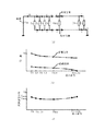
上記(1)の問題に関し、図67、図68を用いて更に詳しく説明する。図67(a),図68(a)は複数の導電性膜(低抵抗化された膜)と配線抵抗及び電源を含む等価回路図であり、図67(b),図68(b)は、各導電性膜(低抵抗化された膜)の高電位側と低電位側の電位を示す図であり、図67(c),図68(c)は、各導電性膜(低抵抗化された膜)の高電位側と低電位側の電位の差電圧、即ち素子印加電圧を示す図である。尚、前述したように、本発明における「導電性膜」あるいは「低抵抗化された膜」は、基本的には、一対の電極間に配置されているものである。そのため、例えば、「「導電性膜」が配線に接続されている状態」とは、厳密に言えば、「「導電性膜」が電極を介して配線に接続されている状態」となる。しかしながら、配線の形状によっては、配線が前記一対の電極を兼ねることもできる。そのため、以下の説明においては、「フォーミング工程」において用いられる「素子」と表記されている対象物は、「一対の電極と、該電極間を接続する低抵抗化された膜(導電性膜)」を指す場合と、「低抵抗化された膜(導電性膜)」を指す場合の双方を含む。
【0023】
図67(a)は、並列接続されたN個の導電性膜D1−DNと電源VEを配線端子TH、TLを通して接続した回路を示すもので、電源の正極を導電性膜D1に、また電源の負極を導電性膜DNに接続したものである。また、各導電性膜を並列に結ぶ共通配線は、図に示すように隣接する導電性膜間で、rの抵抗成分を有するものとする(画像形成装置では、電子線のターゲットとなる画素は、通常、等ピッチで配列されている。従って、電子放出素子も空間的に等間隔をもって配列されており、これらを結ぶ配線は幅や膜厚が製造上ばらつかない限り、素子間でほぼ等しい抵抗値を持つ)。また、導電性膜D1乃至DNは、ほぼ等しい抵抗値Rdを有するものとする。図67(c)から明らかなように、図67(a)のような回路の場合には、両端の導電性膜(D1及びDN)に近い程大きな電圧が印加され、中央部付近の導電性膜では印加電圧が低くなる。
【0024】
一方、図68に示すのは、並列接続された導電性膜列の片側(本図ではD1側)に電源の正負極を接続した場合である。各導電性膜に印加される電圧は、図68(c)に示すようにD1に近い程大きなものとなる。
【0025】
以上二つの例で示したような導電性膜毎の印加電圧のばらつきの程度は、並列接続される導電性膜の総数Nや、導電性膜抵抗Rdと配線抵抗rの比(=Rd/r)や、あるいは、電源の接続位置により異なるが、一般にはNが大きい程、Rd/rが小さい程ばらつきは顕著となり、また、図67よりも図68の接続方法の方が、導電性膜に印加される電圧のばらつきが大きい。また、上記二つの例とは異なるが、図69に示すような単純マトリクス配線においても、配線抵抗rx及びryで生じる電圧降下により、各導電性膜毎の印加電圧にばらつきが生じる。
【0026】
以上説明したように、複数の素子(導電性膜)を共通配線で接続する場合、導電性膜抵抗Rdに対して配線抵抗を十分小さくしないと、導電性膜毎の印加電圧がばらつくことになる。
【0027】
一方、発明者らが鋭意検討した結果、前述した「フォーミング工程」を行う場合、間隙を形成するための、電圧あるいは、電力は、素子の形状即ち、図65に示した導電性膜4の形成材料、膜厚、および寸法W,L1などが同じであれば、同じ電圧あるいは電力で間隙が形成される。この素子固有の電圧あるいは、電力をそれぞれ、素子のフォーミング電圧Vform、フォーミング電力Pformと呼ぶ。このVformあるいはPformより極度に高電圧、高電力を素子(導電性膜)に与えて「フォーミング工程」を行うと、導電性膜に形成される間隙の形態的変化が極度に起こり、電子放出特性が劣化し、それ以下であると、当然のことながら、間隙が形成されないことがわかった。
【0028】
他方、前述した様に、共通配線で結線された複数の導電性膜を、同時に外部の電源より、共通配線を通じた電圧供給で「フォーミング工程」を行う場合、配線での電圧降下により、各素子(各導電性膜)への素子印加電圧に差異が生じ、素子印加電圧が前述のフォーミング電圧Vform、フォーミング電力Pformより過剰の電圧、電力が印加される素子(導電性膜)が発生する。これらの導電性膜に形成される間隙の形状が変化し、「フォーミング工程」を経て得られた複数の電子放出素子の電子放出特性が大きくばらつくことが定性的にわかる。尚、定量的取扱については、後述の実施の形態で述べる。
【0029】
従って、「フォーミング工程」での素子印加電圧(導電性膜に印加される電圧)のばらつきを防止するためには、複数の素子(導電性膜)を結線して電源まで導く共通配線は、低抵抗な配線とする必要が生ずる。また、共通配線に結線された素子数の増加に伴い、その配線への要求は、さらに厳しいものとなる。これは、電子源および画像形成装置の構造設計や製造プロセスの自由度に大幅な制限を付加することになり、ひいては高価な装置になってしまう。
【0030】
次に上記(2)(3)の問題点について更に詳しく説明する。
【0031】
「フォーミング工程」では、導電性膜へ通電することにより間隙を形成するが、共通配線、および素子では、通電により電力が消費され、ジュール熱に変換され、基板温度の上昇を伴う、一方、間隙形成の際の形態的変化は、温度の影響も受けやすい。従って、基板温度のばらつきや変動は、素子の電子放出特性に影響を与えることになる。特に複数の素子を配置した電子源および画像形成装置においては、同時に「フォーミング工程」を行う素子数の増加を伴い、前述の共通配線での電圧降下によるばらつきだけでなく、問題が大きくなる。例えば、基板の中央部と、熱の逃げが存在する端部とで基板の上昇温度に分布が発生し、中央部の温度が端部より上昇してしまい、電子放出特性のばらつきを生ずることとなる。結果として、各素子の電子放出特性のばらつきにより、画像形成装置にした場合は輝度に差が出るなどの不都合が起きてしまい、画像品位が低下する。
【0032】
また同時に、これら発生した熱は、基板に対して熱的衝撃あるいは歪を与え、特に、真空装置とした画像形成装置で、大気の圧力に耐える容器構造とした場合には破損などの安全性の問題を生ずる。
【0033】
以上のような問題により、更には以下の不都合が発生する。
(1)共通配線することが可能な素子(導電性膜)の数が事実上、制限されてしまう。
(2)配線抵抗を低くするために、AuやAgなど比較的高価な材料を使用する必要が生じ、原材料費が上昇する。
(3)配線抵抗を低くするために配線を厚く形成する必要が生じ、電極の形成やパターニングといった製造プロセスに要する時間や装置設備の値段を増大させる。
【0034】
【課題を解決するための手段】
本発明は上述した課題を解決するために鋭意検討を行ってなされたものであり、下述する構成のものである。
【0035】
即ち、本発明は、電子源の製造方法であって、
基体上に、各々が一対の電極と該電極間を接続する高分子膜とからなる複数のユニットと、該各ユニットの電極に接続された配線とを配置する工程と、
前記複数のユニットの各々を構成する前記高分子膜を、全て、低抵抗化し、カーボン膜にせしめる第1の工程と、
前記カーボン膜に、前記配線を介して電圧を印加することにより前記カーボン膜の一部に間隙を形成する第2の工程とを有し、
前記第2の工程は、前記第1の工程の後に行われることを特徴とする。
【0036】
上記本発明の電子源の製造方法においては、前記第1の工程が、前記高分子膜に電子ビーム、光またはイオンビームを照射する工程により行われることが好ましい。
【0037】
また、前記各ユニットの電極に接続された配線を、行方向配線、列方向配線からなるマトリクス配線で構成することが好ましい。
【0038】
また、本発明は前記間隙を形成する工程である第2の工程(フォーミング手段)に特徴があり、以下これを具体的に説明する。
【0039】
A.各行方向配線または各列方向配線に結線された、高分子膜が低抵抗化された膜を有する各ユニットに対して順次フォーミングを行なう。つまり、所望の部分の素子(高分子膜が低抵抗化された膜)群にのみ電圧が印加され、それ以外の素子群に電圧が印加されないようにする。
【0040】
B.所望の部分の素子(高分子膜が低抵抗化された膜)群がフォーミングされる際、各素子がほぼ同じ電圧、あるいは同じ電力でフォーミングされるようにする。
【0041】
上記Aに関し、更に具体的に説明する。
【0042】
A−1.前記間隙を形成する工程において、前記行方向配線と前記列方向配線のうちいずれか一方の配線群の全てに電位V1を印加し、他方の配線群のうち一部の配線にV1とは異なる電位V2を印加し、残りの配線にV1を印加する、もしくはこれを繰り返す。
【0043】
この場合、前記電圧V2を印加する側の配線群は、前記配線に結線された複数の各素子(各高分子膜が低抵抗化された膜)に印加される電力のばらつきが小さい方の配線群であることが好ましい。
【0044】
具体的には、前記間隙を形成する工程を、例えば、前記行方向配線または前記列方向配線の片端に接続された給電部からの電力供給によって行なう場合、
行方向に並設された、高分子膜が低抵抗化された膜の数をNx、列方向に並設された、高分子膜が低抵抗化された膜の数をNy、行方向の1素子当たりの配線抵抗をrx、列方向の1素子当たりの配線抵抗をryとすると、
(Nx×Nx−8Nx)×rx≦(Ny×Ny−8Ny)×ry
のとき行方向配線の片端に接続された給電部からの電力供給によって行ない、
(Nx×Nx−8Nx)×rx>(Ny×Ny−8Ny)×ry
のとき列方向配線の片端に接続された給電部からの電力供給によって行なう。
【0045】
また、前記間隙を形成する工程を、例えば、前記行方向配線または前記列方向配線の両端に接続された給電部からの電力供給によって行なう場合、
行方向に並設された膜(高分子膜が低抵抗化された膜)の数をNx、列方向に並設された膜(高分子膜が低抵抗化された膜)の数をNy、行方向の1素子当たりの配線抵抗をrx、列方向の1素子当たりの配線抵抗をryとすると、
(Nx×Nx−24Nx)×rx≦(Ny×Ny−24Ny)×ry
のとき行方向配線の両端に接続された給電部からの電力供給によって行ない、
(Nx×Nx−24Nx)×rx>(Ny×Ny−24Ny)×ry
のとき列方向配線の両端に接続された給電部からの電力供給によって行なう。
【0046】
A−2.前記間隙を形成する工程において、前記行方向配線うち一部の配線に電位V1を印加し、残りの配線にV1とは異なるV2を印加し、前記列方向配線のうち一部の配線に電位V1を印加し、残りの配線にV1とは異なるV2を印加する。この場合、前記間隙を形成する工程は、前記行方向配線と前記列方向配線とに結線された、高分子膜が低抵抗化された膜の複数を一群とする、2つに分割された各ユニットに対して行われる。
【0047】
次に、上記Bに関し、更に具体的に説明する。
【0048】
B−1.前記間隙の形成工程を、前記配線に接触配置された電気的接続手段からの通電により行う。つまり、共通配線の端子からフォーミング時の電圧を給電するのではなく、これとは別に設けられた電気的接続手段を介してフォーミング電圧を印加する。
【0049】
この場合、
「前記電気的接続手段は、前記配線の複数箇所に接触配置されること」、
「前記電気的接続手段は、前記配線の複数箇所に接触配置される複数の接触端子を有すること」、
「前記電気的接続手段は、前記配線の表面に亙って接触可能な接触面を有すること」、
「前記電気的接続手段は、前記配線の抵抗よりも低抵抗な部材を含むこと」、
「前記電気的接続手段の温度制御を行うこと」、
「前記電気的接続手段が接触配置される前記配線表面部分には、低抵抗金属が被覆されていること」、
「前記電気的接続手段が接触配置される前記配線が、絶縁部材により被覆された下層配線であって、該絶縁部材には、前記電気的接続手段と前記下層配線との接触を可能とするコンタクトホールが形成されていること」、
「前記間隙を形成する工程は、前記配線に接触配置された電気的接続手段からの電力供給に加えて、前記配線の片端もしくは両端に接続された給電部からの電力供給によって行われること」、
などが好ましい実施形態として挙げられる。
【0050】
B−2.前記行方向または列方向の配線の少なくとも一方を所定間隔で分割する、あるいは高インピーダンス部分を設けた構成で、その一部にフォーミング電圧を印加し、フォーミング処理を終了後、分割部あるいは高インピーダンス部を接続する。
【0051】
具体的には、例えば、前記行方向または列方向の配線の少なくとも一方を所定間隔で分割するすることにより前記複数ユニット間を電気的に開放しておき、この状態で各ユニットに対して前記間隙を形成する工程を行った後に、各ユニット間を電気的に接続する短絡工程を設ける。
この場合、
「前記複数の膜(高分子膜が低抵抗化された膜)が結線された配線が所望の間隔で電気的に開放され、該膜(高分子膜が低抵抗化された膜)が複数ユニットに分割されている各ユニットに対して行われる間隙を形成する工程の後に、前記短絡工程を有すること」、
「前記短絡工程は、低抵抗金属材料によるワイヤーボンディング工程であること、もしくは、低融点金属を加熱溶融させることで各ユニットを電気的に短絡させる工程であること」、
などが好ましい実施形態として挙げられる。
【0052】
また、例えば、前記行方向または列方向の配線の少なくとも一方に所定間隔で高インピーダンス部分を設けておき、この状態で各ユニットに対して前記間隙を形成する工程を行った後に、各ユニット間を電気的に短絡する。
この場合、
「前記複数の膜(高分子膜が低抵抗化された膜)が結線された配線が所望の間隔で高インピーダンス部分を介して接続され、該膜が複数ユニットに分割されている各ユニットに対して行われる間隙を形成する工程の後に、各ユニットを電気的に短絡すること」、
「前記短絡工程は、低抵抗金属材料によるワイヤーボンディング工程であること、もしくは、低融点金属を加熱溶融させることで各ユニットを電気的に短絡させる工程であること」、
「前記高インピーダンス部分は、高抵抗率の金属、もしくは、ニッケル・クロム合金薄膜からなること」、
「前記高インピーダンス部分は、接続周囲の前記配線より幅が狭いこと、もしくは、接続周囲の前記配線より厚さが薄いこと」、
などが好ましい実施形態として挙げられる。
【0053】
B−3.前記間隙を形成する工程を、前記配線を通じて前記各膜(高分子膜が低抵抗化された膜)に電力を供給することにより行う場合において、前記各膜(高分子膜が低抵抗化された膜)への印加電力あるいは印加電圧が実質的に一定となるように制御する。
【0054】
この場合、前記印加電力あるいは印加電圧の制御は、前記各膜(高分子膜が低抵抗化された膜)に前記間隙が形成される前に随時行われることが好ましく、具体的には、前記配線に結線された複数の膜(高分子膜が低抵抗化された膜)のうち、前記間隙が形成される前の膜(高分子膜が低抵抗化された膜)の位置を検知し、前記位置に応じて他の膜(高分子膜が低抵抗化された膜)に間隙を形成するのに要する印加電力あるいは印加電圧の制御を行うのが好ましい。
【0055】
また、前記間隙を形成する工程を例えば前記配線の片側に接続された給電部からの電力供給により行う場合には、前記配線に結線された前記複数の膜(高分子膜が低抵抗化された膜)のうち該配線の両端部に位置する膜から中央部に位置する膜に向けて前記給電部に印加する電圧が大きくなるように印加電圧の制御を行うのが好ましい。
【0056】
また、前記間隙を形成する工程を例えば前記配線の両端に接続された給電部からの電力供給により行う場合には、前記配線に結線された前記複数の膜(高分子膜が低抵抗化された膜)のうち該配線の一端と中央部とに位置する膜から配線の1/4の長付近に位置する膜に向けて前記給電部に印加する電圧が大きくなるように印加電圧の制御を行うのが好ましい。
【0057】
また、本発明の電子源の製造方法においては、前記間隙を形成する工程において、基板温度のばらつきや変動が最小限になるように所定のユニット単位でフォーミングを行うことが好ましい。
【0058】
具体的には、前記間隙を形成する工程において、複数の行方向配線又は/及び複数の列方向配線に結線された複数の膜(高分子膜が低抵抗化された膜)を1ユニットとし、各ユニットに対して順次電圧を印加する。
この場合、
「前記間隙を形成する工程において、1つのユニットに振り分けられた配線と、該ユニットに続いて電圧が印加される別のユニットに振り分けられた配線との間に、他のユニットに振り分けられた配線が配置されること」、
「前記間隙を形成する工程において、行方向配線の総数がGNであって、行方向配線番号を端から順に1、2、3、4、…、GNと名前を付ける場合、該行方向配線番号をユニットの総数UNで割った余りの数に応じて、1つのユニットに振り分けられる行方向配線を分類すること」、
「前記間隙を形成する工程において、列方向配線の総数がRNであって、列方向配線番号を端から順に1、2、3、4、…、RNと名前を付ける場合、該列方向配線番号をユニットの総数UNで割った余りの数に応じて、1つのユニットに振り分けられる列方向配線を分類すること」、
「前記間隙を形成する工程において、各ユニット内に振り分けられた配線に対して同時に電圧を印加すること」、
「前記間隙を形成する工程において、各ユニット内に振り分けられた配線に対して順次電圧を印加すること」、
「前記間隙を形成する工程において、前記1つのユニットに前記電圧を印加する期間が終了した後で、引き続いて、前記別のユニットに前記電圧を印加する期間を開始すること」、
「前記間隙を形成する工程における電圧印加は、予め決められたインターバルを置いて複数回行われること」、
「前記間隙を形成する工程において、1つのユニットに対する電圧印加中に、残るその他のユニットへの電圧印加が行われること」、
などが好ましい実施形態として挙げられる。
【0059】
また、本発明は、基体上に配置された複数の電子放出素子を有する電子源と、該電子源からの電子線の照射により画像を形成する画像形成部材とを有する画像形成装置の製造方法であって、前記電子源を上述した本発明の電子源の製造方法にて製造することを特徴とする。
【0060】
尚、上記本発明におけるフォーミング手段A−1,A−2,B−1,B−2,B−3は、それぞれ個別に実施しても効果があるが、適宜併用して実施されても良い。
【0061】
本発明によれば、導電性膜を形成する工程、有機化合物を含む雰囲気を形成する工程(あるいは、導電性膜上に高分子膜を形成する工程)、導電性膜に通電することでカーボン膜を形成すると同時に、該カーボン膜に間隙を形成する工程、を必要としていた従来の電子源の製造方法に比べて、その工程を大幅に簡素化することができる。
【0062】
また、本発明によれば、電子源の製造工程である導電性膜に間隙を形成する工程における前述したような様々な課題を解決することができる。つまり、素子膜(高分子膜が低抵抗化された膜)への間隙の形成において、低抵抗化された膜への電圧、電流の回り込みを防止し、配線による電圧降下によるフォーミング電圧或は電力の分布を減少せしめるなどして、各電子放出素子の特性のバラツキを抑制することができる。
【0063】
【発明の実施の形態】
以下、本発明の実施形態例を説明するが、本発明はこれらの形態例に限定されるものではない。
【0064】
まず始めに、「▲1▼電子放出素子の作成方法」について示し、その後、「▲2▼多数素子で構成される電子源・画像形成装置のフォーミング方法及び手段」について詳細に説明する。
【0065】
▲1▼電子放出素子の作成方法
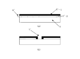
図1は、本発明の製造方法により製造される電子放出素子102を用いた画像形成装置の一例を示す模式図である。尚、図1では画像形成装置(気密容器100)内を説明するために、後述する支持枠72およびフェースプレート71の一部を取り除いた図である。
【0066】
図1において、1は電子放出素子102が多数配置された基板(リアプレートと呼ぶ)である。71は、画像形成部材75が配置されたフェースプレートである。72は、フェースプレート71とリアプレート1間を減圧状態に保持するための支持枠である。101はフェースプレート71とリアプレート1間の間隔を保持するために、配置されたスペーサである。
【0067】
画像形成装置100がディスプレイの場合には、画像形成部材75は蛍光体膜74とメタルバックなどの導電性膜73から構成される。62および63はそれぞれ電子放出素子102に電圧を印加するために接続された配線である。Doy1〜DoynおよびDox1〜Doxmは、画像形成装置100の外部に配置される駆動回路などと、画像形成装置の減圧空間(フェースプレートとリアプレートと支持枠とで囲まれる空間)から外部に導出された配線62および63の端部とを接続するための取り出し配線である。
【0068】
電子放出素子102をより詳細に示したのが図2である。尚、図2(a)は平面図、図2(b)は断面図である。
【0069】
図2において、1は基体(リアプレート)、2と3は電極(素子電極)、6’はカーボン膜、5’は間隙である。また、カーボン膜6’は、電極2、3間の基体1上に配置されている。そして、カーボン膜6’は電極2、3の一部を覆うことにより、各々の電極2,3との確実な接続が可能となっている。
【0070】
上記カーボン膜は「炭素を主成分とする導電性膜」あるいは「一部に間隙を有し、一対の電極間を電気的に繋ぐ炭素を主成分とする導電性膜」ということもできる。あるいはまた、「一対の炭素を主成分とする導電性膜」ということもできる。
【0071】
上記のように構成される電子放出素子では、間隙5’に十分な電界が印加されたときに電子が間隙5’をトンネルして、電極2、3間に電流が流れる。このトンネル電子の一部が散乱により放出電子となる。
【0072】
従って、カーボン膜6’は必ずしも全体が導電性を有していなくても、少なくとも一部が導電性を有していればよい。かかる膜6’が絶縁体であると、電極2,3間に電位差を与えても、間隙5’に電界がかからず、電子を放出せしめることができないためである。カーボン膜6’は、好ましくは、少なくとも電極2(および電極3)と間隙5’との間の領域が、導電性を有しており、この様な構成とすることで間隙5’に十分な電界を与えることができる。
【0073】
図3は、本発明の電子放出素子の製造方法の一例を示したものである。以下に、図1及び図2を用いて、本発明の電子放出素子の製造方法の一例を説明する。
【0074】
(1)ガラスなどからなる基板(基体)1を洗剤、純水および有機溶剤等を用いて十分に洗浄し、真空蒸着法、スパッタ法等により電極材料を堆積後、例えばフォトリソグラフィー技術を用いて基体1上に電極2、3を形成する(図3(a))。ここで、電極材料としては、後述のようにレーザー照射プロセスを行う場合など、必要に応じて、透明導体である酸化物導電体、すなわち、酸化スズ、酸化インジウム(ITO)等の膜を用いることができる。
【0075】
(2)電極2、3を設けた基体1上に、電極2,3間を繋ぐ高分子膜6”を形成する(図3(b))。この高分子膜6”としてはポリイミドが好ましい。
【0076】
高分子膜6”の形成方法は、公知の種々の方法、すなわち、回転塗布法、印刷法、ディッピング法等を用いることができる。特に、印刷法によれば、所望の高分子膜6”の形状をパターニング手段を用いずに形成できるため、好ましい手法である。中でも、インクジェット方式の印刷法を用いれば、直接、数百μm以下のパターンの形成も可能であるため、フラットディスプレイパネルに適用されるような、高密度に電子放出素子を配置した電子源の製造に対しても有効である。
【0077】
インクジェット方式によって高分子膜6”を形成する場合、高分子材料の溶液を液滴付与し、乾燥させればよいが、必要に応じて、所望の高分子の前駆体溶液を液滴付与し、加熱等により高分子化させることもできる。
【0078】
本発明においては、上記高分子材料としては、芳香族系高分子が好ましく用いられるが、これらの多くは溶媒に溶けにくいため、その前駆体溶液を塗布する手法が有効である。一例を挙げれば、インクジェット方式により芳香族ポリイミドの前駆体であるポリアミック酸溶液を塗布(液滴付与)して、加熱等によりポリイミド膜を形成することができる。
【0079】
なお、高分子の前駆体を溶かす溶媒としては、例えば、N−メチルピロリドン、N,N−ジメチルアセトアミド、N,N−ジメチルホルムアミド、ジメチルスルホキシドなどが使用でき、また、n−ブチルセロソルブ、トリエタノールアミンなどと併用することもできるが、本発明が適用できれば特に制限は無く、これらの溶媒に限定されるわけではない。
【0080】
本発明において、特に芳香族ポリイミドは比較的低温で炭素間の結合の解離、再結合によって導電性が発現しやすい、すなわち炭素原子間の二重結合が生成しやすい高分子であるため、高分子膜6”として好ましい材料である。また、ポリフェニレンオキサジアゾール、ポリフェニレンビニレンも熱分解により導電性が発現するため本発明における高分子膜6”として好ましく用いることができる。
【0081】
(3)次に、高分子膜6”を低抵抗化せしめる「低抵抗化処理」を行う。「低抵抗化処理」は、高分子膜6”に導電性を発現せしめ、高分子膜6”を炭素を主成分とする導電性膜(高分子膜が低抵抗化した膜)6’とする処理である。この工程では、後述の間隙形成工程の観点から、高分子膜6”のシート抵抗が、103Ω/□以上107Ω/□以下の範囲に下がるまで低抵抗化処理を行う。この「低抵抗化処理」の一例としては、高分子膜6”を加熱する事により高分子膜6”を低抵抗化することができる。加熱により高分子膜6”が低抵抗化する(導電化する)理由としては、高分子膜6”内の炭素原子間の結合の解離、再結合を行うことで導電性を発現する。
【0082】
加熱による「低抵抗化処理」は、前記高分子膜6”を構成する高分子を分解温度以上の温度で加熱することで達成することができる。また、上記高分子膜6”の加熱は不活性ガス雰囲気中や真空中といった酸化抑制雰囲気下において行うことが特に好ましい。
【0083】
前述した芳香族高分子、特に芳香族ポリイミドは、高い熱分解温度を有するが、その熱分解温度を超えた温度、典型的には、700℃から800℃以上で加熱することにより、高い導電性を発現せしめることができる。
【0084】
しかしながら、本発明のように、電子放出素子を構成する部材である高分子膜6”が熱分解するまでの加熱を行う場合、オーブンやホットプレートなどによって全体を加熱する方法では、電子放出素子を構成する他の部材の耐熱性の観点から、制約を受ける場合がある。特に、基体1においては、石英ガラスやセラミックス基板など、特に高い耐熱性を有するものに限定され、大面積のディスプレイパネル等への適用を考えると、非常に高価なものになってしまう。
【0085】
そこで、本発明では、図3(c)に示す様に、より好適な低抵抗化処理の方法として、電子ビームやイオンビームや光を照射することにより行う。照射する光としてはレーザビームやハロゲン光を用いることができる。そして、特には、電子ビームまたはレーザービーム照射手段10から電子ビームまたはレーザービームを高分子膜6”に照射することにより、該高分子膜6”を低抵抗化することが好ましい。このようにすれば、特別な基板を用いることなく、高分子膜6”を低抵抗化することが可能となる。また、この場合、熱以外の要因、例えば電子線による分解再結合、光子による分解再結合が、熱による分解再結合に加味されるためにより好ましい結果を導いている可能性もある。
【0086】
低抵抗化処理を行う過程を以下に説明する。
【0087】
(電子ビーム照射を行う場合)
電子ビームを照射する場合は、電極2,3、高分子膜6”を形成した基体1を、電子銃が装着されている減圧雰囲気下(真空容器内)にセットする。容器内に設置された電子銃から高分子膜6”に対して電子ビームを照射する。この時の電子ビームの照射条件としては、加速電圧Vac=0.5kV以上10kV以下であることが好ましい。また、この電子線を照射している間、電極2、3間の抵抗値をモニターし、所望の抵抗値が得られた時点で電子線照射を終了することが好ましい。
【0088】
(レーザービーム照射を行う場合)
レーザービームを照射する場合は、電極2,3、高分子膜6”を形成した基体1を、ステージ上に配置し、高分子膜6”に対してレーザービームを照射する。このとき、レーザーを照射する環境は、高分子膜6”の酸化(燃焼)を抑制するため、不活性ガス中や真空中で行うのが好ましいが、レーザーの照射条件によっては、大気中で行うことも可能である。
【0089】
この時のレーザービームの照射条件としては、例えば、パルスYAGレーザの第二高調波(波長532nm)を用いて照射することが好ましい。また、このレーザーを照射している間、電極2、3間の抵抗値をモニターし、所望の抵抗値が得られた時点でレーザービーム照射を終了することが好ましい。
【0090】
なお、照射するレーザ光に対して、高分子膜6”を構成する材料の方が、電極2,3を構成する材料よりも光の吸収性が高い材料を選択することで、実質的に高分子膜6”のみを加熱することが、より好ましい。
【0091】
また前記電子ビームあるいはレーザービーム照射は、高分子膜6”全体に渡って行う必要は必ずしもない。高分子膜6”の一部分を低抵抗化しておくことによっても、以後の工程を行うことができる。
【0092】
(4)次に、前記工程(3)により得られた導電性膜6’(高分子膜が低抵抗化された膜)に、間隙5’の形成を行う(図3(d))。この工程(「フォーミング工程」)により、間隙を有するカーボン膜を得ることができる。
【0093】
ここでは多数の素子に対する工程ではなく、単素子に対する工程を説明する。多数の素子の工程については、実施例においてより詳細に説明する。
【0094】
この間隙5’の形成は、電極2、3間に電圧を印加する(電流を流す)ことによって行なわれる。尚、印加する電圧としてはパルス電圧であることが好ましい。この電圧印加工程により、導電性膜6’(低抵抗化された膜)の一部に間隙5’が形成される。
【0095】
パルス電圧の例を図16に示す。T1及びT2は電圧波形のパルス幅とパルス間隔であり、T1を1マイクロ秒〜10ミリ秒、T2を10マイクロ秒〜100ミリ秒とし、矩形波の波高値(フォーミング時のピーク電圧)は適宜選択して、例えば数十秒間から数十分程度印加する。
【0096】
以上の説明では間隙(電子放出部)を形成する際に、素子の電極間に矩形波パルスを印加してフォーミング処理を行っているが、素子の電極間に印加する波形は矩形波に限定することはなく、三角波など所望の波形を用いてもよく、その波高値及びパルス幅・パルス間隔等についても上述の値に限ることなく、電子放出部が良好に形成されるものであればよい。
【0097】
なお、この電圧印加工程は、前述の低抵抗化処理と同時に、すなわち、電子ビームあるいはレーザービームの照射を行っている最中に、電極2、3間に電圧パルスを連続的に印加することによっても行うことができる。いずれの場合においても、電圧印加工程は、減圧雰囲気下、好ましくは1.3×10⁻³Pa以下の圧力の雰囲気中で行うのが望ましい。
【0098】
上記の電圧印加工程においては、導電性膜6’(低抵抗化された膜)の抵抗値に応じた電流が流れる。従って、導電性膜6’の抵抗が極端に低い状態、すなわち、低抵抗化が過剰に進んだ状態であると、間隙5’の形成に多大な電力が必要となる。比較的小さいエネルギーで間隙5’の形成を行うためには、低抵抗化の進行度合を調整することで可能である。そのため、低抵抗化処理は、高分子膜6”の全領域に渡って均一に行われることが最も好ましいが、高分子膜6”の一部にのみ低抵抗化処理を施すことでも対処しうる。
【0099】
本発明の電子放出素子が真空雰囲気中で駆動されることを加味すると、絶縁体が真空雰囲気中に露出することは好ましくない。そこで、前記電子ビームまたはレーザビームの照射によって、高分子膜6”の実質的な全表面を改質(低抵抗化)することが好ましい。
【0100】
図4は、前記「低抵抗化処理」により、高分子膜6”の表面のみ低抵抗化し、間隙5’を形成する過程を示した模式図(断面図)である。図4(a)は電圧印加工程前(「低抵抗化処理」後)、図4(b)は電圧印加工程終了時を示している。
【0101】
図4(a)において、1は基板、6’−1は「低抵抗化処理」により低抵抗化された領域であり、6’−2は低抵抗化されていない領域である。図4(b)において5’は間隙である。
【0102】
まず、低抵抗化処理された表面領域6’−1に、電圧印加工程により電流が主に流れ、表面領域6’−1の一部に間隙5’の起点が形成される。そして、電圧印加工程を続けることで、電流は形成された間隙5’の起点を避け、周辺部に回り込むことで生じる熱によって、熱分解を起こしていなかった下層の高分子領域6’−2も徐々に熱分解される。そして、間隙5’の起点となった部位から導電性膜6’の厚み方向に間隙が成長し、間隙5’が形成される(図4(b))。
【0103】
なお、低抵抗化した領域6’−1が、基板1側であったり、膜厚の中間の位置であっても、最終的に、導電性膜6’の厚み方向に渡って、間隙5’を形成することができる。
【0104】
図5は、高分子膜6”の基板表面に平行な方向で、その一部を低抵抗化した場合の模式図(平面図)を示しており、図5(a)は電圧印加工程前、図5(b)は電圧印加工程開始直後、図5(c)は電圧印加工程終了時である。
【0105】
まず、低抵抗化された領域6’に、電圧印加工程により電流が流れ、間隙5’の起点となる狭い間隙5”が形成される(図5(b))。形成された狭い間隙5”を避けて電流が流れるため狭い間隙5”の周辺部が加熱され、熱分解を起こしていなかった領域も徐々に熱分解され、最終的に、基板表面と実質的に平行な方向における、高分子膜6”の全体に渡り、間隙5’が形成される(図5(c))。
【0106】
なお、上記のように、部分的に熱分解を行った高分子膜を用いたほうが、良好な電子放出特性を示す場合が多い。この理由は明確ではないが、未分解の高分子が、熱拡散によって間隙5’近傍に移動しやすいために、より電子放出に良好な間隙が形成、保持され、駆動による劣化の少ない構造になっていると思われる。
【0107】
以上のような工程を経て得られた電子放出素子を図6に示した測定装置によってその電圧−電流特性を計測したところ、その特性は、図7に示したようなものである。図6において、図2などで用いた符合と同じ符号を用いた部材は、同じ部材を指す。54はアノードであり、53は高圧電源、52は電子放出素子から放出された放出電流Ieを測定するための電流計、51は電子放出素子に駆動電圧Vfを印加するための電源、50は電極2,3間を流れる素子電流を測定するための電流計である。上記電子放出素子は、しきい値電圧Vthを持っており、この電圧より低い電圧を電極2,3間に印加しても、電子は実質的に放出されないが、この電圧より高い電圧を印加することによって、素子からの放出電流(Ie)、電極2,3間を流れる素子電流(If)が生じはじめる。
【0108】
この特性のため、同一基板上にマトリックス状に上記電子放出素子を複数配した電子源を構成し、所望の素子を選択して駆動する単純マトリックス駆動が可能である。
【0109】
次に、図1に示した、上記電子放出素子を用いた本発明の画像形成装置の製造方法の一例を図8乃至図15などを用いて以下に示す。
【0110】
(A)まず、リアプレート1を用意する。リアプレート1としては、絶縁性材料からなるものを用い、特には、ガラスが好ましく用いられる。
【0111】
(B)次に、リアプレート1上に、図2で説明した一対の電極2,3を複数組み形成する(図8)。電極材料は、導電性材料であれば良い。また、電極2,3の形成方法は、スパッタ法、CVD法、印刷法など種々の製造方法を用いることができる。なお、図8では、説明を簡略化するために、X方向に3組、Y方向に3組、合計9組の電極対を形成した例を用いているが、この電極対の数は、画像形成装置の解像度に応じて適宜設定される。
【0112】
(C)次に、電極3の一部を覆うように、下配線62を形成する(図9)。下配線62の形成方法は、様々な手法を用いることができるが、好ましくは印刷法を用いる。印刷法のなかでもスクリーン印刷法が大面積の基板に安価に形成できるので好ましい。
【0113】
(D)下配線62と、次工程で形成する上配線63との交差部に絶縁層64を形成する(図10)。絶縁層64の形成方法も様々な手法を用いることができるが、好ましくは印刷法を用いる。印刷法のなかでもスクリーン印刷法が大面積の基板に安価に形成できるので好ましい。
【0114】
(E)次に、電極2の一部を覆うように、下配線62と実質的に直交する上配線63を形成する(図11)。上配線63の形成方法も様々な手法を用いることができるが、下配線62と同様、好ましくは印刷法を用いる。印刷法のなかでもスクリーン印刷法が大面積の基板に安価に形成できるので好ましい。
【0115】
(F)次に、各電極対2、3間を接続するように、高分子膜6”を形成する(図12)。高分子膜6”は、前述のように様々な方法で作成することができるが、大面積に簡易に形成するには、インクジェット法を用いることが好ましい。
【0116】
(G)続いて、前述した様に、高分子膜6”を低抵抗化する「低抵抗処理」を行う。全てのユニット(高分子膜と一対の電極から構成される)の、高分子膜6”の低抵抗化を行う。「低抵抗化処理」については、前記した電子ビームやイオンビームなどの粒子ビームを照射するか、レーザビームを照射することにより行われる。この「低抵抗化処理」は好ましくは減圧雰囲気中で行われる。この工程により、高分子膜6”に導電性が付与され、導電性膜6’に変化する(図13)。具体的には、導電性膜6’の抵抗値としては、103Ω/□以上107Ω/□以下の範囲となる。
【0117】
(H)次に、前記工程(G)により得られた導電性膜6’(高分子膜が低抵抗化された膜)に、間隙5’の形成を行う。この間隙5’の形成は、各配線62および配線63に電圧を印加することによって行う。これにより、各電極対2、3間に電圧が印加される。尚、印加する電圧としてはパルス電圧であることが好ましい。この電圧印加工程により、導電性膜6’の一部に間隙5’が形成される(図14)。
【0118】
なお、この電圧印加工程は、前述の低抵抗化処理と同時に、すなわち、電子ビームあるいはレーザービームの照射を行っている最中に、電極2、3間に電圧パルスを連続的に印加することによっても行うことができる。いずれの場合においても、電圧印加工程は、減圧雰囲気下で行うのが望ましい。
【0119】
(I)次に、予め用意しておいた、アルミニウム膜からなるメタルバック73と蛍光体膜74とを有するフェースプレート71と、上記工程(A)〜(H)を経たリアプレート1とを、メタルバックと電子放出素子が対向するように、位置合わせする(図15(a))。支持枠72とフェースプレート71との当接面(当接領域)には接合部材が配置される。同様に、リアプレート1と支持枠72との当接面(当接領域)にも接合部材が配置される。上記接合部材には、真空を保持する機能と接着機能とを有するものが用いられ、具体的にはフリットガラスやインジウム、インジウム合金などが用いられる。
【0120】
図15においては、支持枠72が、予め上記工程(A)〜(H)を経たリアプレート1上に接合部材によって固定(接着)された例を図示しているが、必ずしも本工程(I)時に接合されている必要はない。また、同様に、図15においてはスペーサ101がリアプレート1上に固定された例を示しているが、スペーサ101も、本工程(I)時にリアプレート1に必ずしも固定されている必要はない。
【0121】
また、図15では、便宜上、リアプレート1を下方に配置し、フェースプレート71をリアプレート1の上方に配置した例を示したが、どちらが上であっても構わない。
【0122】
さらには、図15では、支持枠72およびスペーサ101は、予め、リアプレート1上に固定(接着)しておいた例を示したが、次の「封着工程」時に固定(接着)されるよう、リアプレート上またはフェースプレート上に載置するだけでもよい。
【0123】
(J)次に、封着工程を行う。上記工程(I)で対向して配置されたフェースプレート71とリアプレート1とを、その対向方向に加圧しながら、少なくとも前記接合部材を加熱する。上記加熱は、熱的な歪を低減するために、フェースプレートおよびリアプレートの全面を加熱することが好ましい。
【0124】
尚、本発明においては、上記「封着工程」は、減圧(真空)雰囲気中あるいは非酸化雰囲気中にて行うことが好ましい。具体的な減圧(真空)雰囲気としては、10-5Pa以下、好ましくは10-6Pa以下の圧力が好ましい。
【0125】
この封着工程により、フェースプレート71と支持枠72とリアプレート1との当接部が気密に接合され、同時に、内部が高真空に維持された、図1に示した気密容器(画像形成装置)100が得られる。
【0126】
ここでは、減圧(真空)雰囲気中あるいは非酸化雰囲気中にて「封着工程」を行う例を示した。しかしながら、大気中で上記「封着工程」を行っても良い。この場合は、別途、フェースプレートとリアプレート間の空間を排気するための排気管を、気密容器100に設けておき、上記「封着工程」後に、気密容器内部を10-5Pa以下に排気する。その後、排気管を封止することで内部が高真空に維持された気密容器(画像形成装置)100が得ることができる。
【0127】
上記「封着工程」を真空中にて行う場合には、画像形成装置(気密容器)100内部を高真空に維持するために、上記工程(I)と工程(J)との間に、前記メタルバック73上(メタルバックのリアプレート1と対向する面上)にゲッター材を被覆する工程を設けることが好ましい。この時、用いるゲッター材としては、被覆を簡易にする理由から蒸発型のゲッターであることが好ましい。したがって、バリウムをゲッター膜としてメタルバック73上に被覆することが好ましい。また、このゲッターの被覆工程は、上記工程(J)と同様に、減圧(真空)雰囲気中で行われる。
【0128】
また、ここで説明した画像形成装置の例では、フェースプレート71とリアプレート1との間には、スペーサ101を配置した。しかしながら、画像形成装置の大きさが小さい場合には、スペーサ101は必ずしも必要としない。また、リアプレート1とフェースプレート71との間隔が数百μm程度であれば支持枠72を用いずに、接合部材によって直接リアプレート1とフェースプレート71とを接合することも可能である。そのような場合には、接合部材が支持枠72の代替部材を兼ねる。
【0129】
また、本実施形態においては、電子放出素子102の間隙5’を形成する工程(工程(H))の後に、位置合わせ工程(工程(I))および封着工程(工程(J))を行った。しかしながら、工程(H)を、封着工程(工程J)の後に行うこともできる。
【0130】
▲2▼多数素子で構成される電子源・画像形成装置のフォーミング方法及び手段
以下では、具体的なフォーミング方法、手段について示す。
【0131】
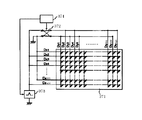
前述した手段のうち、まず(A−1)について説明する。
【0132】
単純マトリクス配置した電子源を図17に示す。この図では、X方向配線112とY方向配線113によって素子114が結線されている。図17に示した単純マトリクス配置の電子源において、X方向の配線端子Dx1からDxmまですべてに電位V2を印加すると共に、任意に選択した少なくとも1本以上のY方向配線端子Dyiに、V2とは異なる電位V1を印加し、残りのY方向配線端子すべてに電位V2を印加するというものである。本例によれば、任意に選択したY方向配線に接続している素子にのみ(V1−V2)[V]の電圧が印加され、他の非選択素子には(V2−V2=0)[V]の電圧が印加されて、フォーミングが行われ、この工程が順次繰り返されることによりフォーミングが終了する(これをライン・フォーミングと呼ぶ)。
【0133】
即ち、選択されていない素子の電極がフローティング(電位不定)状態になったり、フォーミングを実施中の素子に印加している電圧がマトリクス配線を介して回り込むことがないため、フォーミングを実施していない素子が静電気により破壊もしくは損傷したり、フォーミング中の素子に印加中の電圧の影響を受けて、電子放出部が変質したりすることを防止でき、各素子の特性を均一にできることになる。
【0134】
ここで、前記電位V1及びV2は必ずしも時間的に変動のない一定電位(DC)に限るものではなく、三角波あるいは矩形波等のパルス状の波形も含むものである。また、上記V1、V2の両方をDC波形あるいはパルス状の波形としたり、どちらか片方をパルス状の波形としてもよい。この時、フォーミング処理を実施しようとする素子に印加される電圧(V1−V2)[V]は、フォーミングにより間隙(電子放出部)を形成するに足りる電圧波形が供給されていればよく、パルス状波形の場合には、上記(V1−V2)[V]はピーク電圧をいうものである。
【0135】
また、フォーミング処理を実施するために任意に選択される列は、同時に1列であっても複数列であってもよく、同時に複数列を選択する場合は、フォーミングにより発生する熱による基板内の温度分布を考慮して、温度分布を均一化するのが好ましい。例えば、図17のようなm行n列のマトリクス基板において、同時に選択する列が10列の場合は、INT(n/10)列間隔に列を選択すればよい。INT(n/10)とは、n/10を小数点第1の位で四捨五入した値を示す関数である。
【0136】
また、複数列を同時にフォーミングする場合、フォーミングに要する時間を短縮できるものの、電圧源には大きな電流容量が必要となる。従って、本例では、フォーミングに要する時間と電圧源の電流容量とを考慮し、最も経済的効果の高い数を選択し、並列でのフォーミングを行うことが望ましい。
【0137】
さらに上述したX方向配線とY方向配線のいずれを選択し、ラインフォーミングをするかについては以下のようにして決定するのが好ましい。
【0138】
単純マトリクス配置した電子源を用いた表示装置の等価回路を図18に示す。Rが素子抵抗、rx,ryが1画素あたりの横あるいは縦方向配線抵抗である。また、横方向(行方向)の素子数をNx、縦方向(列方向)の素子数をNyとする。この電子源をフォーミング処理する際、通常1列あるいは1行ずつを一括してフォーミングする。なお、ここでいう一括フォーミングとは、多数の素子に対して所定の給電部(1ケ所あるいは複数)から電力を供給してフォーミングすることを指しており、必ずしも多数の素子を同時にフォーミングすることを意味するものではない。
【0139】
ラインフォーミングを模式的に示したのが図19の等価回路である。ここで表示装置(パネル)外の配線等のインピーダンスはrx,ry,Rに比べ無視できるとしている。ここでは横方向(接地部からkライン目)に一括してラインフォーミングする例を示す。
【0140】
図19からも明らかなように、素子抵抗R、配線抵抗rx,ryにばらつきがない場合、各素子にかかる電圧は必ず給電部に最も近い素子のそれが最大となる。また、フォーミングされた素子の抵抗はフォーミング前の抵抗Rに比べて2〜3桁以上も大きい。従って、ラインフォーミングすると給電側から順次切れていく(複数の、高分子膜が低抵抗化された膜に、間隙が順次形成される。)。そして、(n−1)番目まで切れていて、次にn番目の素子をフォーミングする時の等価回路は図20となる。即ち、この状態でも最も給電部に近いn番目の素子が切れて、次の時点での等価回路は図20よりも1素子少ない梯子状のものとなる。(n−1)番目の素子まで切れている状態で、給電部に一定の電圧V0を印加したとすると、n番目の素子にかかる電圧は次式で与えられる。
V(k,n)={1−k×ry/R−n×(Nx−n+1)×rx/R}V0……(1)
【0141】
なお、上式の導出は、一般的な4端子マトリクスの(N−n)段のシリーズとして容易に計算できる。ここで、rx,ryはRに比べ十分小さいとした。また、これを電力で現すと、n番目の素子にかかる電力は次式で与えられる。

つまり、V,Pはk,nの関数であり、ラインフォーミングの方向の素子アドレスnの2次、他方向の素子アドレスkの1次で変化することがわかる。図21に電圧あるいは電力のパネル内分布の模式図を示す。
【0143】
上記のようなラインフォーミング方法には、次のような問題点がある。即ち、図21にみられるように給電部に一定の電圧を供給しても素子のアドレスによってその素子が切れる時(カーボン膜に間隙が形成される時)にかかる電圧、及び電力に差がでてしまう。この現象は画素数が大きくなり、また配線抵抗が素子抵抗に比べ大きくなってくるとより大きな影響を及ぼす。
【0144】
各素子が切れる直前に印加される電力のn方向の最大最小の差は次式となる。即ち、電力最大となるのは給電端(n=1)の時で、最小となるのは中央部(n=Nx/2)のときであり、P0=V0×V0/Rとして、
P(k,1)−P(k,Nx/2)〜Nx×Nx/2×(rx/R)×P0……(3)
但し、Nx≫1である。
【0145】
また、k方向の最大・最小の差は、最大となるのが給電端(k=1)で、最小となるのが接地端(k=Ny)であるから、次式となる。
P(1,n)−P(Ny,n)〜2×Ny×(ry/R)×P0 ……(4)
但し、Ny≫1である。
【0146】
上記2式よりわかるように、特にラインフォーミング方向の画素数が大きくなると急激に画素間のフォーミング条件に差がでてくることになる。従って、大画面化に際して無視できない悪影響を及ぼすことになる。
【0147】
図21の例は、給電部が行(あるいは列)の1端にある場合であるが、給電部が両端にある場合は、系の対称性から、一括フォーミングされる行(あるいは列)の両端部及び中央部で各素子が切れる直前に印加される電力が大きく、両端から1/4ライン長付近では小さくなり、やはり素子アドレスによってばらつきが生じてしまう。ここで、給電方式を一般化するために、新たにN'を導入する。この時、片側給電の場合N'=N,両側給電の場合N'=N/2。
【0148】
結局、単純マトリクスをラインフォーミングする場合、給電部に一定の電圧V0を印加したとき、n番目の素子にかかる電力は次式で与えられる。
n方向の最大最小の差:ΔP=N’×(N’/2)(rx/R)×P0…(6)
k方向の最大最小の差:ΔP=2×Ny×(ry/R)×P0 ……(7)
【0149】
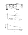
尚、両側給電の場合は、n≦Nx/2に対して、n>Nx/2でも対応する。さらに、素子が単純マトリクス配列ではなく、1次元梯子状に配列された場合も同様の問題点を有する。図22(a)〜図22(c)に、いくつかの例において、等価回路と給電部に一定電圧を印加した場合に各素子が切れる直前の印加電力の素子アドレスによる違いの例を示す。素子数はN、配線抵抗は1素子あたりr、素子抵抗はRとする。
【0150】
図22(a)は、給電部が梯子状ラインの一端に1ケ所配置され、他端に接地部が1ケ所配置されている例であり、給電部に電圧V0を印加したとき、(n−1)番目まで切れて、n番目が切れる時にかかる電力はnの関数として、
ΔP=P(N)−P(1)=(N+2)×(N−1)×(r/R)×P0……(9)
となる。
【0151】
図22(b)は、給電部と接地部が梯子状ラインの同じ側の端部に配置されている例で、図22(c)は、給電部と接地部が梯子状ラインの両端にそれぞれ1ケ所ずつ配置されている例である。
【0152】
図22(a)の場合と同様にP(n),ΔPを求めると、
P(n)={1−4×n×(N’−n+1)×(r/R)}×P0……(10)
;P0=V0×V0/R
ΔP=P(1)−P(N’/2)=N’×N’×(r/R)×P0…(11)
【0153】
図22(b)の場合N’=N、図22(c)の場合N’=N/2(nはN/2に関して対称に考える)。本図からわかるように、1次元配列の場合においても給電部に一定の電圧を印加しても、各素子が切れる直前に印加される電力は、素子アドレスによってばらつく事になる。
【0154】
従って、素子を2次元に配列した装置を1ラインずつ一括して通電フォーミングする際、各素子に印加される電力のばらつきを小さくできる方向(行あるいは列)を選択してフォーミングすることができればよいわけである。
【0155】
具体的には、2次元の方向をx,y方向とし、各方向の素子数をNx,Ny、各方向の1素子あたりの配線抵抗をrx,ry、給電部がx方向配線あるいはy方向配線の片端にある場合a=8、給電部がx方向配線あるいはy方向配線の両端にある場合a=24としたとき、
(Nx×Nx−a×Nx)×rx≦(Ny×Ny−a×Ny)×ry…(12)
なら、x方向にフォーミングし、
(Nx×Nx−a×Nx)×rx>(Ny×Ny−a×Ny)×ry…(13)
なら、y方向にフォーミングすればよい。尚、ここでは各素子が切れる(間隙が形成される)時にかかる電力によって方向を決定した。
【0156】
ここで、簡単に上記条件式を説明しておく。
【0157】
通電フォーミングは、熱的な現象と考えられるので、各素子に印加される電力が問題となる。従って、前述の(5)式で考える。ここで、x方向のフォーミングの時は、r=rx,r'=ry,N=Nx、y方向のフォーミングの時は、r=ry,r'=rx,N=Nyとすると、(5)式は下式のようになる。
【0158】
(1)x方向に一括フォーミングする場合、
面内での最大値:
P(1,1)/P0=1−2×Nx×(rx/R)−2×(ry/R)……(16)
面内での最小値:
(2)y方向に一括フォーミングする場合
面内での最大値:
P(1,1)/P0=1−2×(rx/R)−2×Ny×(ry/R)……(20)
面内での最小値:
従って、Px≦Py、つまり、
(Nx×Nx−8×Nx)×rx≦(Ny×Ny−8×Ny)×ry
なら、x方向に一括してフォーミングしたほうがよく、
Px>Py、つまり
(Nx×Nx−8×Nx)×rx>(Ny×Ny−8×Ny)×ry
なら、y方向に一括してフォーミングしたほうがよい。
【0161】
また、図22(b)に示すように、給電部がxあるいはyの両端にある場合、一括してフォーミングするラインの中央に対して対称である事を考えれば、条件式は、(Nx×Nx−24×Nx)×rx、と、(Ny×Ny−24×Ny)×ry、の大小で設定される。
【0162】
以上のように、2方向の配線抵抗と素子数との関係により、ラインフォーミングに適した方向が決まる。フォーミング処理の電圧波形としては図16と同様であり、適宜設定される。
【0163】
続いて、前述した手段のうち(A−2)について説明する。
【0164】
図23に示す構成により行配線(Dx1乃至Dxm)及び列配線(Dy1乃至Dyn)にフォーミング電源(電位はV1またはV2)を接続してフォーミングを行う。この時、全行配線のうちk本に電位V1を、残りの(m−k)本に電位V2を印加し、同様に全列配線のうちL本に電位V2を、残りの(n−L)本に電位V1を印加する。これにより、全素子のうちk×L+(m−k)×(n−L)個の素子が選択され、選択された素子では、図2の素子電極2、3間に電圧V2−V1が印加され、高分子膜が低抵抗化された膜の部位に間隙5’が形成される。
【0165】
次に、列方向配線(あるいは行方向配線)に接続した電位V1とV2とを入れ換えることにより、先に選択されなかった残りの素子が選択され、同時にフォーミングを施すものである。またフォーミング処理の電圧波形としては図16に示すようなものを用いる。
【0166】
前述の手段(A−1)との相違は、(A−1)がライン単位でフォーミングするのに対し、これはブロック単位でフォーミングするところが異なり、効果は(A−1)と同様に、未フォーミング電子放出素子への電圧の回り込みが無くなり、また、同時にフォーミング電圧が印加される素子数が1/2に少なくなることにより、配線を流れる電流値も小さくなるため、配線での電位降下による電子放出特性のばらつきも小さく抑えられる。
【0167】
次に前述の手段のうち(B−1)について説明する。
【0168】
この製造法の特徴を図24(a)のブロック図、及び図24(b)の回路図、そして、図24(c)の素子単体断面図を用いて説明する。
【0169】
図24(a)において、241はマルチ電子源、242は電気的接続手段、243は温度コントローラ、244はフォーミング電源、245は温度検知器、また、実線で囲った部分が通電処理装置246を示している。マルチ電子源241は、前述した素子が複数並んだデバイスで、共通配線で各素子は接続されている。電気的接続手段242はマルチ電子源241の並列した素子の複数部分で、電気的接続を行う機構FCを有するものであり、図24(b)に示したように、マルチ電子源241の各部に抵抗rf1,rf2を介して接続される。ここでこの電気的接続手段242は前記素子の共通配線のような形状の制限(薄膜形状、画像形成装置を想定した場合1画素に納まるサイズ)がないため、抵抗rf1,rf2を共通配線の素子間抵抗rに比較して十分に小さい値にしている。
【0170】
図24(b)のように、1列に並んだ素子の複数部分で接続し、電源VEから電圧を印加したとき、rf2による電位降下の大きさは並列配線数が少なく、抵抗が非常に小さいため十分に小さい値となり、共通配線への接続部に印加される電圧はほぼ等しくなる。また、各接続点からみた並列抵抗は、左右等しい数の素子が接続されるため、どれも等しい値となる。この結果、各素子に直接印加される電圧のばらつきは共通配線を用いて通電した場合に比較して格段に小さくできる。
【0171】
さらに、上記接続機構FCに用いる材料に熱伝導性の良いものを使い、その後段に熱容量の大きなものを設け、加熱、冷却機構及びそれを制御する機構を備えた構成としている。この構成により、上記接続機構FCは素子に通電するためだけではなく熱の伝導路としても働き、素子電極を通して電子放出部の温度を変化させる機能を有するものとなる。
【0172】
素子単体の電気的接続部の模式的断面図を図24(c)に示した。同図において、2及び3は電気的接続を得るための素子電極、5’は間隙(電子放出部)、6’は高分子膜が低抵抗化された膜(カーボン膜)を示し、247は熱伝導路となる電気的接続手段を示している。なお、図24(c)では、素子電極上で電気的接続手段と接続しているが、むろん、配線上で行ってもよい。
【0173】
電気的接続手段247を構成する材料は銅、アルミニウム、インジウム、銀、金、タングステン、モリブデン等の金属や、真鍮、ステンレス等の合金を使用している。また、配線との接触抵抗を小さくし、複数の接触部での接触抵抗の分布を小さく抑えるため、剛性の高い金属の表面を低抵抗金属でコーティングした接続手段を設けたり、各接続手段には、接触する配線に対し数十g以上の荷重がかかる不図示の荷重印加機構を備えていることが望ましい。この荷重印加機構は弾性部材により構成され、例えばコイルバネ、板バネ等が用いられる。
【0174】
また、上記電気的接続手段はマトリクス配線の一列あるいは複数列に接続し、一列あるいは複数列を同時にフォーミングしてから、接続する列をずらし、順次全体をフォーミングするものであるが、電気的接続手段の数を多くすれば全体を同時にフォーミングすることも可能である。
【0175】
さらに、上記した単純マトリクス構成では絶縁層の下層の配線上に電気的接続手段を設ける場合、接触部にコンタクト用の窓を形成することとし、該下層配線の電気的接続手段との接触部には低抵抗金属がコーティングされていることが好ましい。また、上記手段(A−1)と組み合わせることにより、X方向の配線あるいはY方向の配線の一方、即ち、フォーミング電圧を印加するため選択された列の配線にのみ複数の電気的接続手段を設け、同方向の非選択配線及び他方の方向の配線は端子から電圧を印加するだけでも十分効果が期待できる。
【0176】
ここまでは単純なマトリクス配置の電子源におけるフォーミング手段について述べたが、この手段(B−1)は、前述した梯子状配置の電子源に対しても同様に利用可能である。
【0177】
上記構成で、素子電極を冷却しながらフォーミング電圧を印加すると、フォーミング電流Ifによるジュール熱で高分子膜が低抵抗化された膜6’が昇温し、この時の温度プロファイルは従来の方法と比較し、急峻になる。これは素子から発生した熱は基板となる石英あるいはガラスと比較して金属電極からの逃げが大きく、この金属電極を上記接続手段247を通して冷却することで、伝導による熱の逃げの効率が大幅に改善されるためである。
【0178】
本発明者らは、間隙(電子放出部)5’が通電の熱による素子の温度プロファイルのピーク位置で発生することを確認し、この温度が間隙形成の起因であると考えた。
【0179】
従来、電極間隔が10μm以上になると温度プロファイルもブロードになり、そのため間隙(電子放出部)5’のばらつきが顕著になると考えたわけである。よって本例のように、電極の温度を低く制御して温度プロファイルを急峻にすれば電極間隔を広げても電位放出部のばらつきは小さくなるという可能性が生まれる。
【0180】
実際、本例の通電処理方法で温度制御しながらフォーミングしたところ電極間隔を10μm以上に広げても高分子膜が低抵抗化された膜6’の温度プロファイルが急峻で、ピーク領域の幅は狭くなり、その結果、間隙(電子放出部)5’のばらつきが少なく抑えられるようになった。
【0181】
さらに上記構成で複数並んだ素子の各部を一定の温度に制御することも可能となり、従来問題となったマルチ電子源のデバイス中央部、端部の温度差も無くなり、これにより、通電フォーミングによって形成される間隙(電子放出部)5’のばらつきも少なくなった。
【0182】
次に前述の手段のうち(B−2)について説明する。
【0183】
まず、複数個の素子を共通に接続する行または列方向の配線のうち、少なくとも一方を所定間隔で分割した構成、あるいは所定間隔で高インピーダンス部分を設けた構成の実現方法について説明する。
【0184】
図25に梯子状配線、図26に単純マトリクスの一部を分割した形状を示す。これらの図において、251はG(1,1)乃至G(2,6)で示される分割ギャップである。配線はフォトリソ技術あるいは印刷技術により作製されるが、いずれの場合も予めマスクパターンに分割用ギャップ部分を設けておけば、所定間隔で分割ギャップのある配線は容易に得られる。また当然ながら連続した配線を作製しておいて、YAGレーザによる溶融切断、あるいはダイシングソーによる機械的切断を行っても所定間隔で分割ギャップのある配線を得ることができる。
【0185】
次に高インピーダンス部分を設ける方法は以下の方法がある。上述のようにして得られた分割ギャップ上にニッケル−クロム合金薄膜等の抵抗率の高い金属を蒸着してパターニングして得る。また或は連続した配線を作製しておいて、その一部の配線幅を非常に狭くしておく、あるいはフォトリソ技術の中のミリング技術により一様に作製した配線の厚さを一部薄膜化することにより得られる。
【0186】
次にこの構成の基板に給電して、特定の素子にフォーミング電圧を印加し、フォーミング処理を行う。ここで給電方法は、配線端から給電し、配線端に近い分割領域内の素子からフォーミング処理を施して、前述の手段(B−1)で用いる特別な電気的接続手段と同様な手段を用いて給電する。
【0187】
次に所定部分をフォーミングした後、分割ギャップ部分あるいは高インピーダンス部分を短絡する方法について説明する。
【0188】
まず単純にAuやAl材料によるワイヤボンディング、あるいはリボンボンディングにより短絡する方法がある。別の方法として以下の方法がある。まずギャップ部の片側、あるいは高インピーダンス部分近傍、あるいは高インピーダンス部分の一部分に、金−鉛ペーストあるいはInやBiを含む低融点金属をマイクロディスペンサーによる塗布、あるいはフォトリソ技術を用いて製膜しておく。レーザ光や赤外線照射やヒータ加熱によりペーストあるいは低融点金属を加熱融解させて、分割ギャップ部分あるいは高インピーダンス部分をその融解した金属で埋めるようにして短絡(接続)させる。あるいは高インピーダンス部分に電流を集中させることにより、高インピーダンス部分の温度が上昇し、上述の他の加熱方法と同じ結果が得られる。
【0189】
次に前述の手段のうち(B−3)について説明する。
【0190】
単純マトリクス配置あるいは1次元梯子状に配列した各素子がフォーミングされる時点での印加電力あるいは印加電圧が全素子で一定になるように、給電部に印加する電圧を制御しながら、1行あるいは1列を一括してフォーミングする方法を以下に示す。
【0191】
従来の問題点で述べたフォーミングに必要な外部端子供給電圧の変動を考慮すると、一括してフォーミングする行(あるいは列)のうち、どの素子までがフォーミング済なのかを検知しながら給電部に印加する電圧を制御して一括フォーミングを行うことにより、全素子に対して一定のフォーミング条件を保つことができる。
【0192】
2次元単純マトリクス配列の場合においては、給電部が行(あるいは列)の1端にある場合、一括フォーミングする行(あるいは列)の両端部付近にある素子をフォーミングするときは給電部に印加する電圧を小さくし、中央部付近にある素子をフォーミングするときは給電部に印加する電圧を大きくすればよい。また、給電部が行(あるいは列)の両端にある場合、一括フォーミングする行(あるいは列)の両端部及び中央部付近にある素子をフォーミングするときは給電部に印加する電圧を小さくし、両端から1/4ライン長付近にある素子をフォーミングするときは給電部に印加する電圧を大きくすればよい。また、一括してフォーミングされる行(あるいは列)に対向する列(あるいは行)の一端または両端が接地されている場合、一括してフォーミングされる行(あるいは列)が接地端に近い場合は給電部に印加する電圧を小さくし、遠い場合は大きくすればよい。
【0193】
さらに、1次元梯子状に素子が配列されていて、給電部が梯子状ラインの一端に1ケ所配置され他端に接地部が1ケ所配置されている場合、給電端部付近にある素子をフォーミングするときは給電部に印加する電圧を小さくし、接地端部付近にある素子をフォーミングするときは給電部に印加する電圧を大きくする。また、給電部と接地部が梯子状ラインの同じ側の端部に配置されているとき、両端部付近にある素子をフォーミングするときは給電部に印加する電圧を小さくし、ライン中央部付近にある素子をフォーミングするときは給電部に印加する電圧を大きくする。また、給電部と接地部が梯子状の両側にそれぞれ1ケ所ずつ配置されている場合、両端部及び中央部付近にある素子をフォーミングするときは給電部に印加する電圧を小さくし、両端から1/4ライン長付近にある素子をフォーミングするときは給電部に印加する電圧を大きくする。
【0194】
具体的には、例えば、単純マトリクスにおいては、素子アドレス(k,n)の素子を、例えばx方向にフォーミングする時には、(1)式の電圧分布を補って、一定電圧になる様に、給電部には、
【0195】
ブロック数(インピーダンス測定回数)が少なければフォーミング制御のアルゴリズムは容易となり、ライン全体をフォーミングするための時間も短くできる。一方、ブロック数が多ければ、素子間のフォーミング条件のばらつきを小さく抑えることができる。なお、フォーミングパルスの印加方法、素子アドレスの検出方法は上記に限ったものではなく、一定の条件さえ整えば素子アドレスの検出が不要となりうる。
【0196】
上記説明した方法を用いることにより、多数素子で構成される電子源・画像形成装置のフォーミングが行われることを示してきたが、さらに多数の素子をフォーミングする手法について説明する。
【0197】
ここでは、マトリクス配線接続された、高分子膜が低抵抗化された膜について、多数行列配線を同時に駆動することで、さらに短時間にフォーミング工程が終了できる手法について説明する。
【0198】
前記したように、多数本の行列配線に対して電圧印加を行うと、電圧印加による発熱により基板が変形したり、破壊がおこることがあった。かかる課題を詳細に述べるとともに、本発明での実施形態を示す。まず課題を詳細に述べる。
【0199】
図28を参照して、以下、基板の変形・破壊の原因についての本発明者の検討結果について説明する。図中、281は電子源基板であり、その材質は硝子である。282は行方向配線(X方向配線)、283は列方向配線(Y方向配線)であり、図示しない高分子膜が低抵抗化された膜は行方向配線及び列方向配線によってマトリクス状に結線されている。このような構成の電子源基板において、高分子膜が低抵抗化された膜を、たとえば隣接する行方向b本を単位として1番からM/b番のブロックにこれらのブロックを順次切り替えて電圧を印加するものとする。
【0200】
このような電圧印加方法を取った場合、フォーミング電圧を印加したブロックに、高分子膜が低抵抗化された膜を流れる電流すなわちフォーミング電流に伴う発熱が集中し、基板内に急峻な温度勾配が発生する。図28には、例として、ブロック1にフォーミング電圧を印加した時の基板内の温度分布のグラフも示してある。このように基板内に急峻な温度勾配が発生して熱応力が発生するために、基板の変形・破壊が生じることが判明した。そこで本発明では、基板内の熱分布を抑制するように、行方向配線もしくは列方向配線を選択することでこれを回避できる。
【0201】
本発明者は、前記課題は隣接する多数本を同時に駆動した場合に基板の変形が起こることを見出し、同時に駆動する行方向配線(もしくは列方向配線)に数の制限を設けること、また、同時に駆動する行方向配線(もしくは列方向配線)を基板内で間引くことにより課題が解決されることを見出した。その詳細は、以下の実施例で示す。
【0202】
【実施例】
以下、添付図面を参照して本発明の好適な実施例を詳細に説明する。この実施例では電子源及びその製造方法と、これら複数の電子源を用いた画像形成装置について説明する。
【0203】
[実施例1]
本実施例は、前記手段(A−1)により作製した多数の素子を単純マトリクス配置した電子源の例である。
【0204】
電子源の一部の平面図を図29に示す。また、図中のA−A’断面図を図30に示す。但し、図29と図30の記号は同じ物を示している。。ここで1は基板、2,3は素子電極、6’は間隙を含むカーボン膜、62はX方向配線(下配線とも呼ぶ)、63はY方向配線(上配線とも呼ぶ)、64は層間絶縁層、301は素子電極2と下配線62との電気的接続のためのコンタクトホールである。
【0205】
まず、電子放出素子の作成について具体的に、図8〜図14を用いて説明する。これらの図では、説明を簡単に行うために、素子数が9個の場合について示している。本実施例では、実際には300×200個の素子があるマトリクスを作製している。
【0206】
(工程1)
ガラス基板1上に、スパッタリング法により、厚さ100nmのPt膜を堆積し、フォトリソグラフィ技術を用いてPt膜からなる電極2,3を形成した(図8)。なお、電極2、3の電極間距離は10μmとした。
【0207】
(工程2)
次に、スクリーン印刷法によりAgペーストを印刷し、加熱焼成することにより、X方向配線62を形成した(図9)。
【0208】
(工程3)
続いて、X方向配線62とY方向配線63の交差部になる位置に、スクリーン印刷法により絶縁性ペーストを印刷し、加熱焼成して絶縁層64を形成した(図10)。
【0209】
(工程4)
さらに、スクリーン印刷法によりAgペーストを印刷し、加熱焼成することにより、Y方向配線63を形成し、基板1上にマトリックス配線を形成した(図11)。
【0210】
(工程5)
以上のようにしてマトリックス配線を形成した基板1の電極2、3間に跨る位置に、インクジェット法により、ポリイミドの前駆体であるポリアミック酸の3%N−メチルピロリドン/トリエタノールアミン溶液を電極間の中央を中心として塗布した。これを、真空下にて、350℃でベークし、直径約100μm、膜厚300nmの円形のポリイミド膜からなる高分子膜6”を得た(図12)。
【0211】
(工程6)
次に、Ptからなる電極2、3、マトリックス配線62、63、ポリイミド膜からなる高分子膜6”を形成した基板1をステージ上(大気中)にセットし、各々の高分子膜6”に対して、QスイッチパルスNd:YAGレーザ(パルス幅100nm、繰り返し周波数10kHz、ビーム径10μm)の第二高調波(SHG)を照射した。このとき、ステージを移動させ、各々の電極2から3の方向に高分子膜6”に10μmの幅で照射し、各々の高分子膜6”の一部に熱分解の進んだ導電性の領域を形成し、高分子膜が低抵抗化された膜6’を得た(図13)。
【0212】
(工程7)
図31は、本実施例を説明するための図で、素子群のうちの一部に対してフォーミングを行う際の、電気的な接続を示したものである。同図では図示の便宜上、素子を6×6個だけ単純マトリクス配線して示しているが、本実施例では300×200個のマトリクスを作製した。
【0213】
図31に於いては、説明上、素子を区別するためにD(1,1)、D(1,2)、…、D(6,6)の様に、(X,Y)座標で示している。また、図中、Dx1,Dx2,…Dx6は単純マトリクス配線の各配線を示しており、各々端子Pを介して外部と電気的に接続されている。また、VEは電圧源であり、導電性の素子膜(高分子膜が低抵抗化された膜)をフォーミングするのに必要な電圧を発生する能力を有するものである。
【0214】
本図に示すのは、D(1,3)、D(2,3)、D(3,3)、D(4,3)D(5,3)、D(6,3)、…D(300,3)の300素子を同時にフォーミングする場合の電圧印加法である。図に示す様に配線Dx3には、グランドレベル、即ち、0[V]が印加される。一方、X方向の配線のうちDx3以外のもの、即ち、Dx1,Dx2,Dx4,Dx5,Dx6,…Dx200には、電圧源VEより、例えば6Vの電位が印加され、これと同時にDy1,Dy2,Dy3,Dy4,Dy5,Dy6,…Dy300の各配線にも電圧源VEより電位が印加される。
【0215】
この結果、マトリクス配線された複数の素子のうち、選択されたD(1,3)、D(2,3)、D(3,3)、D(4,3)、D(5,3)、D(6,3)、…、D(300,3)の両端には、電圧源VEの出力電圧が印加されるため、これら300素子では平行してフォーミングが行われる。
【0216】
一方、前記300素子以外の素子は、素子両端ともほぼ等電位(電圧源VEの出力電位)が印加されるため、素子両端にかかる電圧はほぼ0[V]となり、フォーミングが行われないのはもちろんのこと、素子膜が変質したり損傷したりすることも全く無い。
【0217】
ここで、各素子の抵抗は約1キロオーム、1素子あたりの下配線抵抗(x方向)は約0.03オーム、上配線抵抗(y方向)は約0.1オームであった。ここで前述したように、給電部が片側の場合では式(12)から、
(Nx×Nx−8Nx)×rx=2628
(Ny×Ny−8Ny)×ry=3840
であるから、素子数は多いがx方向の素子を一括してフォーミングしたほうがよい。
【0218】
本実施例では、上記手順により選択素子に図16に示したような電圧波形のパルスを印加しフォーミング処理を行った。なお、本実施例ではパルス幅T1を1ミリ秒、パルス間隔T2を10ミリ秒とし、矩形波の波高値(フォーミング時のピーク電圧Vpf)は5Vとし、フォーミング処理は約1.3×10⁻⁴Paの真空雰囲気下で60秒間行った。
【0219】
上述の工程で作製した多数の電子放出素子の特性を把握するために、その電子放出特性の測定を前述の図6の測定評価装置を用いて行った。
【0220】
なお測定条件は、アノード電極と電子放出素子間の距離を4mm、アノード電極の電位を1kV、電子放出特性測定時の真空装置内の真空度を1.3×10⁻⁴Paとした。
【0221】
本実施例における代表的な電子放出素子では、素子電圧15V程度から急激に放出電流Ieが増加し、素子電圧20Vでは素子電流Ifが0.1mA、放出電流Ieが1μAとなり、電子放出効率Ie/If(%)は1%であった。
【0222】
本実施例では全ての素子において、電子放出効率のばらつきが非常に低く抑えられ、ほぼ均一な特性が得られた。
【0223】
[実施例2]
本実施例では、実施例1で作製したフォーミング処理を施していない電子源基板を用いて画像形成装置を構成した例について図32及び図33を用いて説明する。
【0224】
図32は、本実施例の画像形成装置の表示パネルを示す模式図である。尚、図32では表示パネル内を説明するために、後述する支持枠322およびフェースプレート326の一部を取り除いた図である。図33は表示パネルに使用される蛍光膜の模式図である。これらの図において図29及び図30に示した部位と同じ部位には同じ符号を付している。
【0225】
本実施例では先のフォーミング処理を施していない300×200個の素子を単純マトリクス配置した電子源基板1をリアプレート321上に固定した後、電子源基板1の5mm上方に、フェースプレート326(ガラス基板323の内面に画像形成部材であるところの蛍光膜324とメタルバック325が形成されている構成される)を支持枠322を介し配置し、フェースプレート326、支持枠322、リアプレート321の接合部にフリットガラスを塗布し、大気中あるいは窒素雰囲気中で、400℃で10分以上焼成することで封着した。また、リアプレート321への電子源基板1の固定もフリットガラスで行った。
【0226】
蛍光膜324は、モノクロームの場合は蛍光体のみで構成することができる。カラーの蛍光膜の場合は、蛍光体の配列により、ブラックストライプ(図33(a))、或いはブラックマトリクス(図33(b))と呼ばれる黒色導電材331と蛍光体332とから構成することができる。
【0227】
本実施例では蛍光体はストライプ形状を採用し、先にブラックストライプを形成し、その間隙部に各色蛍光体を塗布し、蛍光膜324を作製した。ブラックストライプの材料として通常よく用いられている黒鉛を主成分とする材料を用いた。ガラス基板323に蛍光体を塗布する方法はスラリー法を用いた。
【0228】
また、蛍光膜324の内面側設けられるメタルバック325は、蛍光膜作製後、蛍光膜の内面側表面の平滑化処理(通常、「フィルミング」と呼ばれる)を行い、その後Al(アルミニウム)を真空状着することにより作製した。フェースプレートには、更に蛍光膜324の導電性を高めるため、蛍光膜324の外面側に透明電極が設けられている場合もあるが、本実施例ではメタルバック325のみで十分な伝導性が得られたので省略した。前述の封着を行う際、カラーの場合は各色蛍光体と電子放出素子とを対応させなくてはいけないため、十分な位置合わせを行った。
【0229】
以上のようにして完成したガラス容器(外囲器328)内の雰囲気を排気管(図示せず)を通じ真空ポンプにて排気し、1.3×10⁻³Pa程度の真空度に達した後、容器外端子Dox1乃至DoxmとDoy1乃至Doynを通じて、実施例1に示した要領で素子電極間に電圧を印加し、前述の通電処理(フォーミング処理)を行い、高分子膜が低抵抗化された膜6’に間隙5’を形成し、電子放出素子を作製した。
【0230】
次に1.3×10⁻⁴Pa程度の真空度で、不図示の排気管をガスバーナで熱することにより溶着し、外囲器328の封止を行った。
【0231】
最後に封止後の真空度を維持するために、ゲッター処理を行った。これは、封止後に高周波加熱法により、画像形成装置内の所定の位置(不図示)に配置されたゲッターBaを加熱し、蒸着形成した。
【0232】
以上のように完成した本実施例の画像形成装置において、各電子放出素子には、容器外端子Dox1乃至DoxmとDoy1乃至Doynを通じ、走査信号及び変調信号を不図示の信号発生手段によりそれぞれ印加することにより、電子放出させ、高圧端子Hvを介してメタルバック325に高電圧を印加して電子を加速し、蛍光体に衝突させ、励起・発光させることにより画像を表示した。
【0233】
本実施例で作製した画像形成装置において、単純マトリクス配線された多数の電子放出素子を均一にフォーミングできたことにより、素子特性が均一になり表示画像の輝度均一性の大幅な向上が確認された。
【0234】
実際、本実施例の表示装置において、給電部を片側のみにしてx方向で一括してフォーミングしたものと、y方向で一括してフォーミングしたものについて、各電子放出素子に一定電圧を印加し、高圧端子Hvに5k[V]印加して輝度測定したところ、x方向で一括してフォーミングした時の輝度むらに対し、y方向で一括してフォーミングした方は輝度むらが大きかった。即ち、フォーミング前にラインフォーミングすべき方向を決定できたことがわかる。
【0235】
[実施例3]
実施例2と同様、前述の手段(A−1)を用いてフォーミング処理を行って作製した画像形成装置について説明する。但し、本実施例においては実施例2と素子の個数、配線形状、厚みを変えてあり、既述の表現を用いて、Nx=50,rx=0.03オーム、Ny=30,ry=0.1オーム、R=1キロオームの電子源基板を作製した。また、X方向、Y方向それぞれの配線の両端から給電できる構造の画像形成装置とした。
【0236】
先に述べたように給電部が各配線の両側にある場合は式(13)から、
(Nx×Nx−24Nx)×rx=39
(Ny×Ny−24Ny)×ry=18
であるから、Y方向の素子列を一括してフォーミングした方がよいことがわかる。
【0237】
実施例2と同様に、x方向を一括したフォーミング方法と、y方向を一括したフォーミング方法の2種の方法でフォーミング処理した2枚のパネルを比較したところ、やはり、前者の輝度むらが、後者よりも高く、明らかにy方向フォーミング処理したものの方が輝度むらが小さかった。即ち、フォーミング前にラインフォーミングすべき方向を決定できたことがわかる。
【0238】
[実施例4]
本実施例では前述した手段(A−1)を用いてフォーミング処理を行う処理装置について説明する。尚、本実施例で用いた電子放出素子の作成は、フォーミング工程以外は、実施例1と同様であるので説明を省略する。
【0239】
本実施例で用いたフォーミング処理装置の電気回路構成を図34に示す。図中、341は実施例1と同様の工程で作製したm×n個の素子を単純マトリクス配線したフォーミング処理を施していない電子源基板であり、342はスイッチング素子アレイ、343はフォーミングパルス発生器、344は制御回路である。
【0240】
電子源用基板341は図31の場合と同様に、端子Dx1乃至Dxm及びDy1乃至Dynを介して、周辺の電気回路と電気的に接続されるが、このうちDx1乃至Dxmはスイッチング素子アレイ342と接続され、Dy1乃至Dynはフォーミングパルス発生器343の出力と接続される。
【0241】
スイッチング素子アレイ342は、内部にS1乃至Smのm個のスイッチング素子を備え、各スイッチング素子は前記端子Dx1乃至Dxmの各々を、フォーミングパルス発生器343の出力またはグランドレベルかのどちらか一方と接続する機能を持つ。なお、各スイッチング素子は、制御回路344の発生する制御信号SC1に従って動作するものである。
【0242】
また、フォーミングパルス発生器343は、制御回路344の発生する制御信号SC2に従って、電圧パルスを出力する。
【0243】
制御回路344は、前述したようにスイッチング素子アレイ342とフォーミングパルス発生器343の動作を制御するための回路である。
【0244】
以上、各部の機能を説明したが、次に全体の動作を順を追って説明する。
【0245】
まず、フォーミングを開始する前に、制御回路344の制御により、スイッチング素子アレイ342の各スイッチング素子は全てグランドレベル側と接続しており、また、フォーミングパルス発生器343の出力電圧も0[V]、即ち、グランドレベルに保たれている。
【0246】
次に、前記図31で説明したように、素子列の一列を選択してフォーミング処理するために、スイッチング素子アレイ342の中のスイッチング素子のうち、フォーミング処理を行う列と接続している以外のもの全てをフォーミングパルス発生器343側と接続するように、制御回路344は制御信号SC1を発生する(図34ではS3を除く全てのスイッチング素子をフォーミングパルス発生器343側に接続した例を示してある。)。
【0247】
次に、制御回路344はフォーミングパルス発生器343に対して、フォーミングに好適な電圧パルスを出力するよう制御信号SC2を発する。選択された一列の素子のフォーミングが完了したならば、制御回路344はフォーミングパルス発生器343に対して、パルスの発生を中止し、出力電圧が0[V]となるよう制御信号SC2を発生する。更に、スイッチング素子アレイ342に含まれる全てのスイッチング素子をグランドレベル側と接続するよう制御信号SC1を発生する。
【0248】
以上の動作手順により、任意に選択した一列の素子フォーミングが完了する。以下、同様の手順で他の素子列を順次フォーミングすることにより、m×n個の素子を単純マトリクス配線した基板の全素子を均一にフォーミングすることができる。
【0249】
本実施例では、上記手順により100×100個の単純マトリクス基板を用い、選択素子に図16に示したような電圧波形のパルスを印加しフォーミング処理を行った。なお、本実施例ではパルス幅T1を1ミリ秒、パルス間隔T2を10ミリ秒とし、矩形波の波高値(フォーミング時のピーク電圧)は5Vとし、フォーミング処理は約1.3×10⁻⁴Paの真空雰囲気下で60秒間行った。そして、図6のような測定評価装置を用いて測定したところ、作製した電子源中の代表的な素子では、素子電圧15V程度から急激に放出電流Ieが増加し、素子電圧20Vでは素子電流Ifが0.2mA、放出電流Ieが2μAとなり、電子放出効率η=Ie/If(%)は1%であった。
【0250】
従来技術の問題点で述べたような亀裂(間隙)形成のばらつきが発生すると、上記電子放出効率の素子間の均一性が得られなかった。しかし、本実施例のフォーミング装置を用いたフォーミング処理方法によれば、各素子がフォーミングされる瞬間、各素子に実効的に印加される電圧のばらつきは小さくなり、素子特性として電子放出効率の素子間ばらつきも10%以下に抑えられた。
【0251】
[実施例5]
次に実施例1と同様に作製したフォーミング処理を施していない電子源基板を用い、前記手段(A−2)によるフォーミング処理を行い電子源とした例を具体的に説明する。
【0252】
図35は、本実施例を説明するための図で、先述したようにして単純マトリクス配線された素子群のうちの一部に対してフォーミングを行う際の電気的な接続を示したものである。
【0253】
図35に示す構成により、行配線(Dx1乃至Dxm)及び列配線(Dy1乃至Dyn)にフォーミング電源(電位はV1またはV2)を接続してフォーミングを行う。このとき全行配線のうち、K本に電位V1を、残りの(m−K)本に電位V2を印加し、同様に全列配線のうちL本に電位V2を、残りの(n−L)本に電位V1を印加する。これにより全素子のうちK×L+(m−K)×(n−L)個の素子が選択され、選択された素子にはほぼ電圧V2−V1(本実施例では6V)が印加されフォーミングが行われる。
【0254】
本実施例では、上記手順により選択素子に図16に示したような電圧波形のパルスを印加しフォーミング処理を行った。なお、本実施例ではパルス幅T1を1ミリ秒、パルス間隔T2を10ミリ秒とし、矩形波の波高値(フォーミング時のピーク電圧)は6V(V2−V1)とし、フォーミング処理は約1.3×10⁻⁴Paの真空雰囲気下で60秒間行った。
【0255】
一方、上記選択された素子以外の素子の両端の電極には、ほぼ等電位が印加されるため、素子両端にかかる電圧はほぼ0[V]となり、フォーミングが行われないのはもちろんのこと、高分子膜が低抵抗化された膜が変質したり損傷したりする事も全く無い。次に、列配線(あるいは行配線)に接続した電位V1とV2とを入れ換えることにより、先に選択されなかった残りの素子が選択され、同様にフォーミングを施す。
【0256】
上述の行程で、m,nを100、K,Lを50として作製した多数の電子放出素子の特性を把握するために、その電子放出特性の測定を前述の図6の測定評価装置を用いて行った。なお測定条件は、前述の実施例と同じく、アノード電極と電子放出素子間の距離を4mm、アノード電極の電位を1kV、電子放出特性測定時の真空装置内の真空度を約1.3×10⁻⁴Paとした。その結果、電子放出効率η=Ie/If(%)は1%であった。また、全ての素子において、ほぼ均一な特性が得られた。
【0257】
[実施例6]
本実施例では実施例5と同じフォーミング処理を施して作製した画像形成装置について図32を用いて説明する。
【0258】
先の実施例2と同様の構成及び作製方法であるが、100×100個の素子を単純マトリクス配線した電子源基板、つまり実施例5で作製した同じ電子源基板を用いて、フォーミング処理を施していない状態の画像形成装置を作製する。
【0259】
完成したガラス容器(外囲器328)内の雰囲気を排気管(図示せず)を通じ真空ポンプにて排気し、約1.3×10⁻³Paより高い真空度に達した後、容器外端子Dox1乃至DoxmとDoy1乃至Doynを通じ、実施例5で示した要領で素子電極間に電圧を印加し、前述の通電処理(フォーミング処理)を行い、高分子膜が低抵抗化された膜に間隙(電子放出部)を形成し、電子放出素子を作製した。次に、1.3×10⁻⁴Pa程度の真空度で、不図示の排気管をガスバーナーで熱することで溶着し、外囲器の封止を行った。
【0260】
最後に、封止後の真空度を維持するためにゲッタ処理を行った。
【0261】
以上のようにして完成した本実施例の画像形成装置において、電子放出素子には、容器外端子Dox1乃至DoxmとDoy1乃至Doynを通じ、走査信号及び変調信号を不図示の信号発生手段によりそれぞれ印加し、高圧端子Hvを通して、高圧を印加して画像を表示した。
【0262】
本実施例で作製した画像形成装置においても、単純マトリクス配線された多数の電子放出素子を均一にフォーミングできることにより、素子特性が均一になり表示画像の輝度むらが低く抑えられたことが確認された。
【0263】
[実施例7]
実施例1で作製したフォーミング処理を施していない電子源基板を用い、前述した手段(A−2)の方法でフォーミング処理して作製した電子源について説明する。
【0264】
図36は、640×400個の単純マトリクス配線されたフォーミング処理を施していないの素子群のうちの半数に対してフォーミングを行う際の電気的な接続を示したものである。また、図中、Dx1,Dx2,…,Dx400及びDy1,Dy2,…,Dy640は、単純マトリクス配線の各配線を示している。また、V1,V2はフォーミングパルスを発生する電源である。
【0265】
図36は黒丸で示した素子を選択的にフォーミングする場合の電圧印加方法である。即ち、V1をグランドレベル、V2を電位Vformとする。黒丸の素子の両端にはほぼ(V2−V1)の電圧即ち、Vformが、白抜きの素子の両端にはほぼ0[V]の電圧が印加されるので、選択的に黒丸の素子がフォーミングされ、白抜きの素子は変化されない。
【0266】
次に、図37に示すのは、上記の方法でフォーミング処理を行うための電気回路構成の一例であり、図中、371はフォーミング処理を施していない素子を640×400個、単純マトリクス配線した電子源基板であり、また372はスイッチング素子、373はフォーミングパルス発生器、374は制御回路である。電子源基板371の行配線(Dx1,Dx2,…Dx400)のうち奇数番目のグループはグランドレベルに、偶数番目のグループはフォーミングパルス発生器の出力に接続する。列配線(Dy1,Dy2,…Dy640)のうち奇数番目のグループと偶数番目のグループは、それぞれグランドレベルあるいはフォーミングパルス発生器の出力のどちらかに接続される。但し、同時にフォーミングパルス発生器に接続されることはない。
【0267】
スイッチング素子372は、前述の列配線の接続切り換えを制御回路374からの制御信号により行う。フォーミングパルス発生器373は制御回路374の発生する制御信号に従って、前述のフォーミングパルスを出力する。
【0268】
まず、フォーミング開始前、全ての配線はグランドレベルに保たれている。次に、列配線の奇数番目のグループをフォーミングパルス発生器373の出力に、偶数番目のグループをグランドレベルに接続するようにスイッチング素子372に制御回路374から信号が送出される。次に、制御回路374からフォーミングパルス発生器373に信号が送られ、フォーミングが行われる。フォーミングのパルスが選択された素子に印加される。このとき、各行配線には行方向の素子個数640の2分の1である320個分のフォーミング電流が流れ、各列配線には同様に200個分の電流が流れる。選択された全ての素子のフォーミングが終了したならば、スイッチング素子372を切り換えて、列配線の奇数番目をグランドレベルに、偶数番目をフォーミングパルス発生器373の出力に接続することにより残りの素子が選択され、同様にフォーミングパルスを印加してフォーミングを行う。
【0269】
本実施例では、上記手順により選択素子に図16に示したような電圧波形のパルスを印加してフォーミング処理を行った。なお、本実施例ではパルス幅T1を1ミリ秒、パルス間隔T2を10ミリ秒とし、矩形波の波高値(フォーミング時のピーク電圧)は5Vとし、フォーミング処理は約1.3×10⁻⁴Paの真空雰囲気下で60秒行った。
【0270】
また、本実施例においては、フォーミング時に各配線に流れる電流による温度上昇を押さえることができ、配線や基板の破壊は一切生じなかった。更に、図36に示したようにマトリクス配線された多数の素子を千鳥状にフォーミングしたので、温度むらが生ずることもなく、良好にフォーミングを行うことができた。
【0271】
その結果、実施例5と同様にして電子放出特性を測定すると電子放出効率η=Ie/If(%)は1%であった。また、全ての素子において、ほぼ均一な特性が得られた。
【0272】
また、実施例6と同様の構成で作製したフォーミング処理前の画像形成装置に対して、本実施例の方法でフォーミング処理を施して作製した画像形成装置においても、単純マトリクス配線された多数の電子放出素子を均一にフォーミングすることができたことにより、素子特性が均一になり表示画像の輝度むらが非常に低く抑えられたことが確認された。
【0273】
[実施例8]
実施例1から実施例7までは、一部の素子だけにフォーミング電圧を印加するよう外部端子から配線を通して給電する方法に関するものであったが、本実施例は、前記手段(B−1)のフォーミング処理方法により配線以外の電気的接続手段を用いて素子に給電するものである。本実施例で用いるフォーミング方法は配線の並び方には依存せず、前述の梯子状配置や単純マトリクス配置どちらにも実施可能である。
【0274】
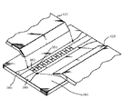
まず電子放出素子を梯子状に配置した電子源の作製方法及び構成を図38を用いて説明する。
【0275】
清浄化した青板ガラス上に厚さ0.5μmのシリコン酸化膜をスパッタ法で形成した基板381上に、厚さ1000ÅのNi薄膜を真空蒸着により成膜し、ホトリソ技術により素子電極(共通配線)385,386を形成する(図38(a))。共通配線385,386間に跨る位置に、インクジェット法により、ポリイミドの前駆体であるポリアミック酸の3%N−メチルピロリドン/トリエタノールアミン溶液を電極間の中央を中心として塗布した。これを、真空下にて、350℃でベークし、直径約100μm、膜厚300nmの円形のポリイミド膜からなる高分子膜382を得た(図38(b))。次に、上記基板381をステージ上(大気中)にセットし、各々の高分子膜382に対して、QスイッチパルスNd:YAGレーザ(パルス幅100nm、繰り返し周波数10kHz、ビーム径10μm)の第二高調波(SHG)を照射した。このとき、ステージを移動させ、共通配線385から386の方向に各々の高分子膜382に10μmの幅で照射し、各々の高分子膜382の一部に熱分解の進んだ導電性の領域を形成した。
【0276】
この複数ライン状に並べたマルチ電子源と、本実施例の核心となるフォーミング用電気的接続手段を用いての通電を説明する斜視図を図39に示す。ここで383は前記素子膜(低高分子膜が抵抗化された膜)であり1000個並列に並んでいる。385と386は各素子に通電する共通配線となるNi電極、391は共通配線385,386の複数部分で電気的接続を行う端子となる針状の銅端子、392は銅端子391とフォーミング電源とを電気的に結ぶ銅のバルク配線を示す。
【0277】
上記銅端子391は素子3つ毎に332組で接続されるよう構成している。上記銅端子を共通配線385,386に圧着し、フォーミング電源から素子のフォーミングに必要な電圧を共通配線385,386に印加して各素子膜383に電子放出部となる間隙(亀裂)384を形成させるものである(図38(c)の断面図及び図38(d)の平面図参照)。このときバルク銅配線392の各端子間での抵抗を共通配線385,386と比較して1/1000以下となるよう、バルク銅配線392の断面は1mm角以上の面積とした。
【0278】
ここで、従来技術の問題点で述べたような間隙形成のばらつきが発生すると、電子放出効率の素子間均一性が得られなかったが、本実施例のフォーミング装置を用いてフォーミング電圧を印加したところ、前記銅端子391の接触部に於ける電圧のばらつきは0.001V以内に納まった。また、実際の素子特性として電子放出効率の素子間ばらつきも3%以下に抑えられた。
【0279】
[実施例9]
本実施例では実施例8の作製工程と同じ工程により作製したフォーミング処理を施していない電子源基板を用いて画像形成装置を構成した例について図40、図41を用いて説明する。
【0280】
図40は本実施例の梯子型配置のマルチ電子源を備えた画像形成装置のパネル構造を示す図であり、図中、VCはガラス製の真空容器で、その一部であるFPは表示面側のフェースプレートを示している。フェースプレートFPの内面には、例えばITOを材料とする透明電極が形成され、更に該透明電極上には赤、緑、青の蛍光体がモザイクもしくはストライプ状に塗り分けられている。図面の複雑化を避けるため、図中では透明電極と蛍光体を合わせてPHとして示されている。なお、各色の蛍光体の間にはCRTの分野では公知のブラックマトリクスもしくはブラックストライプを設けてもよく、また蛍光体の上に同じく公知のメタルバック層を形成することも可能である。前記透明電極は、電子ビームの加速電圧を印加できるように端子EVを通じて真空容器外と電気的に接続されている。本実施例では4k[V]の高圧を印加した。
【0281】
また、Sは真空容器VCの底面に固定されたマルチ電子ビーム源の基板(電子源基板)で、前述のように電子放出素子が配列形成されている。本実施例では実施例8と同様に電気的接続手段を用いたフォーミング処理を窒素雰囲気中で行った電子源基板Sを真空容器VCの底面に固定した。
【0282】
なお、本実施例の電子源基板Sにおいては、1列あたり200素子が並列に配線された素子列が200列設けられている。各素子列の2本の配線電極(共通配線)は、両側のパネル側面に設けられた電極端子Dp1乃至Dp200及びDm1乃至Dm200と交互に接続しており、真空容器外から駆動電気信号が印加できるようになっている。
【0283】
また、電子源基板SとフェースプレートFPの中間には、ストライプ状のグリッド電極GRが設けられている。グリッド電極GRは、前記素子列と直交して(即ちY方向に沿って)200本が独立して設けられている。開口Ghは、各表面伝導型電子放出素子ESに対応して1個ずつ円形のものが設けられているが、場合によってはメッシュ状に多数の通過口を設けることもある。各グリッド電極は、電極端子G1乃至G200により真空容器外と電気的に接続されている。なお、グリッド電極は表面伝導型電子放出素子から放出された電子ビームを変調することができるものであればその形状や設置位置は必ずしも図40のようなものでなくても良く、例えば電子放出素子の周辺や近傍に設けてもよい。
【0284】
本実施例の表示パネルでは、電子放出素子の素子列とグリッド電極で200×200のXYマトリクスを構成している。従って、素子列を1列ずつ順次駆動(走査)していくのに同期して、グリッド電極列に画像1ライン分の変調信号を同時に印加することにより、各電子ビームの蛍光体への照射を制御し、画像を1ラインずつ表示していくことができる。
【0285】
図41は、図40に示した本実施例の表示パネルを駆動するための電気回路をブロック図として示したものある。図中、410は図40に示した表示パネル、411は外部から入力する複合画像信号をデコードするためのデコード回路、412はシリアル/パラレル変換回路、413はラインメモリ、414は変調信号発生回路、415はタイミング制御回路、416は走査信号発生回路である。表示パネル410の電極端子は各々電気回路と接続されており、端子EVは10[kV]の加速電圧を発生する電圧源HVと、端子G1乃至G200は変調信号発生回路414と、端子Dp1乃至Dp200は走査信号発生回路416と、端子Dm1乃至Dm200はグランドとそれぞれ接続されている。
【0286】
以下、各部の機能を説明する。
【0287】
まず、デコード回路411は、外部から入力する例えばNTSCテレビ信号等の複合画像信号をデコードするための回路で、複合画像信号から輝度信号成分と同期信号成分を分離して、前者をDATA信号としてシリアル/パラレル変換回路412に、後者をTsync信号としてタイミング制御回路415に出力する。即ち、デコード回路411は、RGBの各色成分毎の輝度を表示パネル410のカラー画素配列に合わせて配列しシリアル/パラレル変換回路412に順次出力する。また、垂直同期信号と水平同期信号を抽出してタイミング制御回路415に出力する。
【0288】
タイミング制御回路415は、前記同期信号Tsyncを基準にして、各部の動作タイミングを整合させるための各種タイミング制御信号を発生する。つまり、シリアル/パラレル変換回路412に対してはTspを、ラインメモリ413に対してはTmryを、変調信号発生回路414に対してはTmodを、走査信号発生回路416に対してはTscanを出力する。
【0289】
シリアル/パラレル変換回路412は、デコード回路411から入力する輝度信号DATAをタイミング制御回路415より入力されるタイミング信号Tspに基づいて順次サンプリングし、200個の並列信号I1〜I200としてラインメモリ413に出力する。タイミング制御回路415は、画像の1ライン分のデータがシリアル/パラレル変換された時点でラインメモリ413に対して書き込みタイミング制御信号Tmryを出力する。
【0290】
ラインメモリ413は、Tmryを受けるとI1〜I200の内容を記憶して、それをI’1〜I’200として変調信号発生回路414に出力するが、これはラインメモリに次の書き込みタイミング制御信号Tmryが入力されるまで保持される。
【0291】
変調信号発生回路414は、ラインメモリ413より入力される画像1ライン分の輝度データに基づいて、表示パネル410のグリッド電極に印加する変調信号を発生させるための回路であり、タイミング制御回路415の発生するタイミング制御信号Tmodに合わせて変調信号を端子G1〜G200に同時に印加する。変調信号は、画像の輝度データに応じて電圧の大きさを変える電圧変調方式を用いるが、輝度データに応じて電圧パルスの長さを変えるパルス幅変調方式を用いることも可能である。
【0292】
また、走査信号発生回路416は、表示パネル410の電子放出素子の素子列を適宜駆動するための電圧パルスを発生するための回路である。タイミング制御回路415の発生するタイミング制御信号Tscanに合わせて適宜内部のスイッチング回路を切り替え、定電圧源DVの発生する電子放出素子の閾値を上回る適当な駆動電圧VE[V]か、またはグランドレベル(即ち0[V])かを選択して端子Dp1〜Dp200に印加するものである。
【0293】
以上の回路により、表示パネル410には特定のタイミングで駆動信号が印加される。即ち、振幅VE[V]の電圧パルスが画像の1ライン表示時間毎に順次Dp1,Dp2,Dp3,…の順に印加されてゆく。一方、端子Dm1〜Dm200は常にグランドレベル(0[V])と接続されているため、上記電圧パルスにより素子列は第1列目から順次駆動され電子ビームが出力されていく。また、これと同期して変調信号発生回路414から、画像の1ライン分の変調信号が同時に端子G1〜G200に印加される。走査信号が切り替えられるのと同期して順次変調信号も切り替えられ、1画面分の画像が表示されてゆく。これを連続して繰り返し行うことにより、テレビジョン動画の表示が可能なわけである。
【0294】
本実施例で作製された画像形成装置においても、並列梯子状配置された多数の素子を均一にフォーミングすることができたことにより、素子特性が均一になり表示画像の輝度むらが非常に低く抑えられたことが確認された。
【0295】
[実施例10]
本実施例は、実施例8において述べた電気的接続手段である複数の針状の銅端子が横に結がり、一体となった電気的接続手段を用いてフォーミング処理を行ったものである。
【0296】
図42に本実施例を説明する電気的接続手段の斜視図を示す。383は素子膜(高分子膜が低抵抗化された膜)、385と386は共通配線(素子電極)、421は電気的接続手段の接触端子で、実施例8と同様に銅で構成されている。
【0297】
図42に示されるように、実施例8では針状であった接触端子が、ここでは横に繋がったナイフエッジ状の形になっている。このため電気的接続端子間に存在した抵抗はバルク金属で繋がったことによりほぼ0になり、更に素子間の配線抵抗も無視できるようになるため、通電処理時に素子に印加されるフォーミング電圧のばらつきは更に小さくなる。
【0298】
実施例8で用いたのと同じ電子源基板381に対して、該電気的接続手段を用いてフォーミングを行った場合、実施例8では、フォーミング時に各素子に印加される電圧のばらつきは0.001Vであったが、本実施例では0.0001V以内になる。
【0299】
このため、実際の素子特性として電子放出効率(1%)の素子間ばらつきも3%以下に抑えられる。また、実施例9と同様にして画像形成装置を形成すると、多数の電子放出素子を均一にフォーミングすることができることにより、素子特性が均一になり表示画像の輝度むらが3%以下となったことが確認された。
【0300】
[実施例11]
実施例8及び実施例10は、複数の電子放出素子が梯子状に配列接続された構成のマルチ電子源のフォーミングに関するものであったが、本実施例では単純マトリクス型に100×100個の素子を2次元に配線されたマルチ電子源に前記手段(B−1)のフォーミング処理方法を適用した場合について説明する。配線構成及び、電子放出素子は実施例1と同様にして形成され、複数の電子放出素子が並んだ電子源基板に電気的接続手段を接続して、フォーミングを行う工程を図43を用いて説明する。
【0301】
図43(a)はマルチ電子源を上部からみた図を示している。ガラス基板に、前記素子膜436が配置され、それぞれの素子膜は配線435および431に接続されている。配線435と素子膜436を接続するために、引き出し電極432を用いている。本実施例では、素子膜に電圧を印加するために、後述する針状端子を使用し、針状端子(以下プローブと呼ぶ)と配線435、431と接続するための電極パッドをそれぞれ434、433とする。
【0302】
図43(b)は、図43(a)のC−C’断面図を用いて、プローブ437を介して素子膜に通電する様子を示している。
【0303】
ガラス基板439上に引き出し電極432、配線435、431が形成されており、電極パッド433を介してプローブ437から配線431に接続する様子を示している。この図では、配線432との接続について示していないが、同様の方法で接続している。
【0304】
図43(c)を用いてプローブを説明する。千鳥状に2列に配置された電気的接続手段であるプローブ437,438を用いて、1素子に対して1組の割合でプローブを接続し、ある1行に接続されている素子両端近傍に、電位V1、V2を印加する様に、それぞれのプローブを低抵抗配線440、441で接続した図である。各プローブはタングステン材のスプリングピンで、各ピンに数十gの荷重がかかる様に押し当てることにより、接触抵抗は0.1Ω以下となる。本実施例では、更に接触抵抗を下げるためにスプリングピン先端及び配線上でプローブが接触する部分433に低抵抗金属、ここではAuをコーティングした。これにより接触抵抗は0.01Ω以下となった。これらプローブはフォーミングパルスを発生する電源に接続されている。
【0305】
フォーミングパルスは図16に示すパルス波形で、T1を1msec、T2を10msec、ピーク電圧を4Vとした。1行のフォーミングが終了後、プローブを接続する行を変えて順次フォーミングを行い、全素子のフォーミングを完了する。本実施例のフォーミング装置を用いてフォーミング電圧を印加したところ、前記スプリングピンの接触部に於ける電圧のばらつきは0.01V以内におさまり、素子特性として電子放出効率(1%)の素子間ばらつきも4%以下に抑えられた。
【0306】
本実施例では電子放出素子1つに1組のプローブを接続したが、配線抵抗及び、素子抵抗を考慮して複数個おきに接続しても効果は同様に得られる。
【0307】
また本実施例では配線表面が露出している部分にプローブを接触させたが、配線表面が露出していない場合、例えば絶縁層で覆われている場合、プローブ接触部分の絶縁層を除去した基板を作製して、本実施例と同様のフォーミング処理を施すことにより、同様の効果が得られる。
【0308】
[実施例12]
本実施例では実施例11で作製したフォーミング処理を施していない電子源基板を用いて画像形成装置を構成した例について図32を用いて説明する。
【0309】
まず、電子源基板1上に形成した各高分子膜6’に対して実施例11と同様のフォーミング処理を大気中あるいは窒素雰囲気中で行った。そして、このフォーミング処理後の電子源基板1をリアプレート321上に固定した。その後、実施例2と同様の構成、方法により画像形成装置を作製した。
【0310】
以上のように完成した本実施例の画像形成装置において、各表面伝導型電子放出素子には、容器外端子Dox1乃至Doxm、Doy1乃至Doynを通じ、走査信号及び変調信号を不図示の信号発生手段によりそれぞれ印加し、高圧端子Hvを通じて5kVの高圧を印加し、画像を表示した。本実施例で作製した画像形成装置においても、単純マトリクス配線された多数の表面伝導型電子放出素子を均一にフォーミングすることができたことにより、素子特性が均一になり表示画像の輝度むらも非常に少ないものとなったことが確認された。
【0311】
[実施例13]
本実施例も表面伝導型電子放出素子を単純マトリクス配置した電子源に前述の手段(B−1)のフォーミング方法を適用した例であり、電気的接続手段を行あるいは列の一方にのみ設けたフォーミング方法である。配線構成及び、フォーミング処理を施す前の複数素子を備えた電子源基板は実施例1と同様にして形成され、該電子源基板に電流注入端子を接続して、フォーミングを行う工程を図44を用いて説明する。
【0312】
実施例8では、電気的接続手段として正極側と負極側の2組で素子に通電するようにしたが、本実施例では実施例1と同様に、横1列の素子を選択してフォーミングを行った。図44では、m行n列(m=1000、n=1000)のマトリクス配線のL行目に通電していることを示している。選択した1行(図44ではDxLライン)の素子の共通配線の端部を接地し、更に該配線と選択された各素子が接続する部分に、実施例8と同様の電気的接続手段を接続し、該手段も接地する。また、各列配線(Dy1〜Dyn)配線及びDxLライン以外の行配線(Dx1〜DxmでDxL以外)を電位Vfのフォーミング電源に接続している。つまり、列側から印加する電圧と同電位を行側に印加することで、非選択行に電流が流れないようにしている。
【0313】
本実施例において、プローブFCによる電流注入は、L行目での電圧降下を抑制することを目的としている。プローブFCを用いない場合でも、L行目だけを選択的に電圧印加することができるが、配線抵抗rx、ryが大きい場合、所望の電圧を印加できないことがあった。この場合に対応するのが本実施例である。この行配線rxによる電圧降下と、列配線ryによる電圧降下を抑制するために、プローブによる電流注入を行うことが本実施例の特徴である。
【0314】
行配線による電圧降下の補正用に抵抗rf4を、また、列配線による電圧降下を補正用に抵抗rf3を使用して、行列配線内で起こる電圧降下を外部でシミュレートして、注入する電流量を調整している。
【0315】
m,nを1000とした電子源基板に対して、上記方法によりフォーミング処理したところ、前記スプリングピンの接触部に於ける電圧のばらつきは0.01V以内におさまり、実際の素子特性として電子放出効率(1%)の素子間ばらつきも4%以下に抑えられた。
【0316】
また、本実施例により作製された電子源基板を用いて、実施例12と同様に作製された画像形成装置においても、単純マトリクス配線された多数の素子を均一にフォーミングすることができたことにより、素子特性が均一になり表面画像の輝度むらが4%以下となったことが確認された。
【0317】
また、本実施例では選択した各素子に対し1対1で電気的接続手段を設けたが、電気的接続手段が接続点が一点の場合でも印加電圧のばらつきを改善することが可能である。例えば図44の行配線DxLの両端を接地し、該配線の中央部にのみ電気的接触手段を接続してフォーミング処理を行った場合でも、作製された素子の電子放出効率の素子間ばらつきを抑えられた。
【0318】
[実施例14]
本実施例は実施例8において述べた電気的接続手段である銅端子の後段に加熱/冷却器をはさんで熱容量の大きな部分を設けているものである。
【0319】
図45に本実施例を説明する装置斜視図、図46に装置の概要を説明するブロック図を示した。451はガラス基板、452は実施例8と同様の工程で作製した素子膜(高分子膜が低抵抗化された膜)である。453a,453bはNi電極(共通配線)であり、電極間隔L1は20μmとし、素子膜452が1000個一列に並んだ構成となっている。454はフォーミング電圧を印加する電気的接続手段となる針状の銅端子で、素子3個毎に332組並んだ構成となっている。455は前記銅端子454と電気的かつ熱的に結合したバルク導体で、ここでは断面5mm×20mmの銅のバーを用いている。456は加熱/冷却器となるペルチェ素子、457は大熱容量導体となる断面20mm×20mmの銅のバーで、461は放熱器、462はバルク導体455の温度の検出器で、ここでは熱電対を用いている。463は加熱/冷却器456を駆動する温度コントローラ、464はフォーミング電源を示している。
【0320】
上記構成で、銅端子454を共通配線453a,453bに圧着し、フォーミング電源464から素子のフォーミングに必要な電圧を共通配線453a,453bに印加して素子膜452に電子放出部となる間隙(亀裂)を形成させるものである。このとき、銅のバー455の各端子間での抵抗は共通配線453a,453bと比較し、1/1000以下となるため、実施例8と同様、素子に印加されるフォーミング電圧にばらつきは無くなる。
【0321】
また、銅のバー455の熱容量は銅端子454、共通配線453a,453bと比較し、桁違いに大きいので、共通配線と銅端子の接触部の温度は常に一定に保たれることになる。フォーミングによるジュール熱で素子が加熱されても前記熱電対462でモニタし、温度コントローラでペルチェ素子456を制御して銅のバー455を冷却することで、ほぼ一定の温度にマルチ電子源を保つことが可能となる。更に、電極(共通配線)の温度を素子間のばらつきなく、常に低く保てるため、フォーミング中の素子膜452の温度プロファイルは急峻なものとなり、温度がピークとなり、熱破壊が起こる領域は狭く、かつ素子間に於けるその領域の相対的位置も一定になるため、亀裂の位置、形状のばらつきは小さく抑えられることになる。
【0322】
本実施例フォーミング装置を用いて実施例8と同様の電子源基板にフォーミング電圧を印加した場合、前記銅端子454の接触部に於ける電圧のばらつきは0.01V以内に納まり、各素子の温度のばらつきも1℃以内に納まり、電極間隔L1を20μmと広くしたにもかかわらず実際の素子特性として電子放出効率の素子間ばらつきも低く抑えられた。
【0323】
また、本実施例により作製した電子源基板を用いて、実施例12と同様に作製された画像形成装置においても、多数の素子を均一にフォーミングすることができたことにより、素子特性が均一になり表示画像の輝度むらも非常に少ないものとなったことが確認された。
【0324】
[実施例15]
本実施例は前記手段(B−1)のフォーミング処理方法を実際に行う装置に関するものである。配線構成と、フォーミング処理を施す前の素子を実施例1と同様にして形成した電子源基板に対し、複数の電気的接続手段を有するフォーミング機構を用いて、横1列に300個の素子が並んだ1つの配線上に各電気的接続手段を接触させてフォーミングを行う。
【0325】
ここで素子が300個並んだ横1列の素子列に関しては、上記フォーミング機構により一度にフォーミングできるが、本実施例で作製した電子源基板のよう素子列が縦に200行並んでいる場合、1行ずつこの操作を繰り返すと、フォーミング工程に多大な時間がかかり、大量生産には不都合が生じる。そこで上記フォーミング機構を複数用意し、並列に並べて同時に駆動させることで工程時間は短縮される。
【0326】
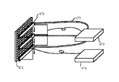
図47に本実施例で用いたフォーミング装置を説明する斜視図を示す。471は単純マトリクス型に素子が並んだマルチ電子源、472は前記電気的接続手段が3つ並列したフォーミング機構、473は温度コントローラ、474はフォーミング電源、475は温度検知器である。
【0327】
図47には3つの前記電気的接続手段が並んだ構成を示したが、これはマルチ電子源471上のスペースと、フォーミング電源474の許容電流量を考慮して適宜設計されるものであり、この電気的接続手段の数は多ければ多い程、工程時間は短縮される。
【0328】
上記構成で実施例12で述べたフォーミング操作を行うと、各表面伝導型電子放出素子の電子放出効率のばらつきは5%以内におさまり、1列ずつ繰り返した場合と比較し、1/3の時間でフォーミングが行える様になった。
【0329】
以上、実施例8から実施例15では、1列に梯子状に並んだマルチ電子源あるいは、単純マトリクス型2次元に並んだマルチ電子源について述べたが、電気的接続手段を使用するこれら実施例の通電方法は、その他の一般的な配線パターンについても同様に使用できるものである。
【0330】
[実施例16]
本実施例は前記手段(B−2)によるフォーミング処理方法の実施例である。
【0331】
先ず、実施例1と同様の手順で図48に示すような単純マトリクス配線パターンを作製する。図48において、481は列方向配線、482は行方向配線、480は素子膜(高分子膜)であり、本実施例では行方向配線482の一部にギャップ483を設けている。
【0332】
次に、上記ギャップ483を高インピーダンス配線で接続する工程について、図49を用いて説明する。尚、図49(a)は図48中のA−A’断面形状を示している。ガラス基板491上に列配線481、行配線482が形成されており、行配線と列配線を電気的に絶縁にするために絶縁膜486を列配線481上に形成している。また行配線のギャップ部483が形成されている。
【0333】
先ず、スパッタ法を用いてニッケル・クロム合金を約2000Å蒸着し、フォトリングラフィ法にてパターニングし、ギャップ483上に高インピーダンス部484を設ける(図49(b))。
【0334】
次に、金−鉛ペースト488をマイクロディスペンサを用いてギャップ部483の片側に塗布する(図49(c))。この状態での回路図を簡単に表したのが図50である。なお、図50では、図示の便宜上、6×6個の素子からなる電子源の例で示しているが、本実施例の実際の電子源は1000×1000個の素子で構成され、X方向のラインDx1〜Dx1000の各配線中に等間隔にそれぞれ10箇所(100素子毎)の高インピーダンス部分(分割部)が設けられている(便宜上、図にはX方向の各配線中にR(1,1)〜R(1,6)及びR(2,1)〜R(2,6)として2素子毎に表現している)。
【0335】
次に、高インピーダンス部分R(1,1)〜R(1,6)より給電部分に近い側に位置する素子、つまりD(1,1)〜D(1,6)及びD(2,1)〜D(2,6)を単素子毎にフォーミングする。図50ではD(1,1)の素子をフォーミングするために、Dx1とDy1との間に電圧をかけている状態を表している。印加する電圧は前述の実施例8と同様のパルス波形を印加する。結果はフォーミング電圧が5Vで、その時の電流は分割がない時の電流値の4分の1となった。
【0336】
その後に基板491の裏面よりレーザ光を当て高インピーダンス部分R(1,1)〜R(1,6)のニッケル−クロム薄膜484を昇温させ、金−鉛ペースト488を溶解させる。この溶解したペースト部分を489で示す(図49(d))。このようにして、図50に示した各X方向ラインの分割部、即ち高インピーダンス部分R(1,1)〜R(1,6)が低抵抗導電体により接続される。
【0337】
その後、次の領域、つまり図50のD(3,1)〜D(3,6)、D(4,1)〜D(4,6)の素子について同様にフォーミング処理を行う。そして、次に分割部R(2,1)〜R(2,6)を上記と同様に低抵抗化する。これを繰り返し全素子に対してフォーミング処理を施す。その結果、図51に示すように、各素子膜(高分子膜が低抵抗化された膜)480に間隙(電子放出部)511が形成され、単純マトリクス状に配線された表面伝導型電子放出素子を有する電子源が得られる。
【0338】
以上の様にして作成された電子源について、図6に示した評価装置により電子放出特性の測定が行った。その結果、電子放出効率η=Ie/If(%)は1%であった。またそのばらつきはパネル全体でも非常に低く抑えられている。
【0339】
本実施例では高インピーダンス部分で区切られた領域内で1素子毎にフォーミングする場合について述べたが、該領域内で実施例1の様に1行を選択し、一括してフォーミングすることも可能で、この場合電子放出効率のばらつきは基板全体でも低く抑えられた。
【0340】
[実施例17]
本実施例では実施例16で作製したフォーミング処理を施していない電子源基板を用いて画像形成装置を構成した例について図32を用いて説明する。
【0341】
まず、実施例16と同様のフォーミング処理を大気中あるいは窒素雰囲気中で行いリアプレート321上に固定し、画像形成装置を作製する。この完成した本実施例の画像形成装置において、各電子放出素子には、容器外端子Dox1乃至Doxm、Doy1乃至Doynを通じ、走査信号及び変調信号を不図示の信号発生手段によりそれぞれ印加し、高圧端子Hvを通じて5kVの高圧を印加し、画像を表示した。
【0342】
本実施例で作製した画像形成装置においても、単純マトリクス配線された多数の表面伝導型電子放出素子を均一にフォーミングすることができたことにより、素子特性が均一になり表示画像の輝度むらが3%以下となったことが確認された。
【0343】
本実施例では、フォーミング処理を行った後に、電子源基板をリアプレートに固定し画像形成装置を作製したが、フォーミング処理前の電子源基板を用いて画像形成装置を構成し、その後、容器外端子Dox1乃至Doxm、Doy1乃至Doynを通じ通電することによりフォーミングを行い、また高インピーダンス部分の低抵抗化は、リアプレートを通してレーザ光で加熱することにより行っても、本実施例と同様に素子特性のばらつきを5%以下に抑えられた。
【0344】
[実施例18]
本実施例は、前記手段(B−2)のフォーミング処理方法を適用した別の実施例である。
【0345】
本実施例による電子源の平面図を図52に示す。本実施例では図52に示すように電子放出素子524を梯子状に1次元配線し、配線523の一部にギャップ251を設けてある。図25はギャップ付配線が完成した状態の回路図を簡単に表したものである。図示の便宜上、画素数を6×6とし、各ブロックを2素子ずつに分割して示しているが、ここで用いた電子源は、1列に1000個の素子が配線された列が1000列あるもので配線を等間隔に10等分(100素子ずつ)分割したものである。尚、ギャップ付配線を製作する工程については実施例16に準ずるものである。
【0346】
本実施例におけるフォーミング処理及びフォーミング処理を実施した後のギャップ251を接続する工程について、図52、図53(a),(b)、図54(a),(b)を用いて説明する。図53(a)はフォーミング処理前のギャップ部251廻りの断面図であり、図53(b)はフォーミング処理を実施した後のギャップ251を接続した状態を示す断面図である。また、図54(a)は梯子状に1次元配列された素子列に対してフォーミング処理を行う様子を示す平面図であり、図54(b)は図54(a)中のA−A’断面図である。
【0347】
本実施例では、実施例8で用いたのと同じマルチプローブ542を用い、図54のプローブ接続点541にプローブ542を接続しフォーミング電源543を接続して1ライン状の素子に対して同時にフォーミング処理を行う。この電圧印加方法を図47に示す。各フォーミング電圧は5Vでその時の各ブロック(100素子)毎の電流は約0.3Aであった。これは分割がない場合の十分の一に当たる。
【0348】
次に図53(b)に示す通り、ギャップ251を1箇所につき3本の直径30ミクロンの金ワイヤー522にてボンディングして接続してマルチ電子源基板を完成した。
【0349】
本発明の基本思想によれば素子の構造、材料、製造方法により必ずしもこれに決まるものではない。従って分割の大きさは1素子あたりのフォーミング電流に応じて決定すれば良い。
【0350】
本実施例の電子源について実施例16と同様にして1素子あたりの素子特性を測定すると、電子放出効率η=Ie/If(%)は平均1%であった。またそのばらつきはパネル全体でも非常に低く抑えられている。
【0351】
本実施例のフォーミング処理方法で実施例9と同様にして形成した画像形成装置においても、並列梯子状配置された多数の素子を均一にフォーミングすることができたことにより、素子特性が均一になり表示画像の輝度むらが3%以下となったことが確認された。
【0352】
[実施例19]
本実施例は、電子放出素子を単純マトリクス配置した電子源を前記手段(B−3)のフォーミング処理方法を適用して作製した実施例である。
【0353】
前述の実施例1と同様の工程によりフォーミング処理を施していない素子膜(高分子膜)を単純マトリクス配線した電子源基板を作製する。なお、本実施例では100×100個の素子を配線した単純マトリクス構成のものを作製した。また、各素子の抵抗は未フォーミングの状態で約1キロオーム、1素子当たりのX方向配線(下配線)抵抗とY方向配線(上配線)抵抗は共に約0.01オームであった。
【0354】
以上に様にして作製した電子源基板を2台用意し、以下に示す異なる2方法によりフォーミングを行った。
【0355】
(フォーミング方法1:本実施例)
本フォーミング方法を図55を用いて説明する。上記の様にして作製した電子源用基板551のY方向配線につながる接続端子Doy1乃至Doykが順次給電部555となる様に(図ではDoykが給電部)、接続を制御する外部スキャン回路552と、電圧源553を接続し、X方向配線につながる接続端子Dox1乃至DoxNを接地した。ここで、電流モニタ回路554により給電部を流れる電流をモニタできる様にしておき、フォーミング処理の対象となる1ラインのインピーダンスを検知できる様にしてある。
【0356】
次に、図56(a)に示すフォーミング波形を印加し、フォーミングを行った。ここで、T1は1ミリ秒、T2は10ミリ秒、Nは10とした。またブロック数は10とした。kライン、mブロックをフォーミングするときに、給電部Doykに印加する電圧(ピーク値)を、
V0(k,m)=8.5×{1+k/10000+0.05m−0.001m×m};m=1〜10とした。
【0357】
ここで、インピーダンスの測定は、図56(a)のN個のフォーミングパルス印加後に、先の印加電圧V0(k,m)よりも低い電圧Viを印加して、まだフォーミングされていない素子に影響を与えることなく、インピーダンス測定を行う。ここで、測定されたインピーダンスが、フォーミングの対象となっているkライン、mブロックがフォーミングされたと判断されたインピーダンスよりも低い場合、対象となっている素子はまだフォーミング終了していないと判断し、図56(b)に示すように追加のフォーミングパルスを発生する。
【0358】
(フォーミング方法2:参考例)
前述の様にして作製したもう1枚の電子源基板に対して、上記フォーミング方法1と同じ構成で回路を接続する。但し、本方法では電流モニタ回路は動作させず、図16に示すフォーミング波形で、T1を1ミリ秒、T2を10ミリ秒、ピーク電圧値は9.3Vで一定として電圧を印加し、一括フォーミングを行った。
【0359】
以上の様に完成したマルチ電子源(フォーミング方法1によるもの、フォーミング方法2によるもの)において、各表面伝導型電子放出素子には端子Dox1乃至DoxN、Doy1乃至DoyKを通じ、実施例16と同様にして、1素子あたりの素子特性を測定した結果、本実施例のフォーミング方法1によるものは電子放出効率η=Ie/If(%)は1%であった。またそのばらつきはパネル全体で3%以下に抑えられている。それに対し、フォーミング方法2によるものは、電子放出効率η=Ie/If(%)は同じく1%であったものの、そのばらつきはパネル全体で10%以上であった。
【0360】
なお本実施例ではアドレスの検出をインピーダンス測定により行ったが、配線の電位分布からアドレスを検知する手段を図57を用いて説明する。
【0361】
フォーミング前後で各素子のインピーダンスが変化することにより、フォーミングが終了すると素子の近傍の配線の電位が大きく変化する(図57(b))。この変化を検出する、つまりプローブピン571を配線に接続し、配線の電位分布の変化を検出することによってもフォーミングされた素子のアドレスを検知できる。
【0362】
[実施例20]
本実施例は、前記手段(B−3)のフォーミング処理方法を適用して作製した梯子状配置の電子源を用いて、図40に示したような画像形成装置を構成した例である。
【0363】
本実施例では絶縁性基板上にフォーミング前の電子放出素子(素子膜)を作製した。作製工程は実施例8と同様である。このフォーミング前の素子膜の寸法等も実施例8と同様である。但し、1列の素子数は200であり、電極の給電部と接地部はラインの両端部に各1カ所ずつ設けた。尚、等価回路は図22(c)で表されたものと同様である。
【0364】
このように作製された電子源基板に対して、図58に示すフォーミング波形でフォーミングを行った。このパルス群のピーク値は8Vから徐々に大きくなり、最大9Vであり、その後徐々に減少して再び8Vになる過程を2度繰り返している。T1は1ミリ秒、T2は10ミリ秒で2度繰り返しの全過程は約5秒であった。ここで用いた電圧値は種々の検討条件の中から最適なものを選択した。その結果、電子放出効率のばらつきが低く抑えられ、素子毎に極めて均一な電子放出特性を有することがわかった。本実施例では既にフォーミングされてしまった素子のアドレスを検出することなく、良好な一括フォーミングが行えた。
【0365】
ここで示した電圧印加方法は、本実施例だけではなく、前記した実施例1乃至実施例19においてもより好適に実施される。
【0366】
[実施例21]
本実施例では、多数の素子をマトリクス配線接続してなる電子源基板に対して、多数本の行方向配線もしくは列方向配線を同時に電圧印加してフォーミング処理する例について説明する。
【0367】
前述の実施例1と同様の工程によりフォーミング処理を施していない素子膜(高分子膜が低抵抗化された膜)を単純マトリクス配線した電子源基板を作製する。なお、本実施例では1024×3072個の素子を配線した単純マトリクス構成のものを作製した。また、各素子の抵抗は未フォーミングの状態で約1キロオーム、1素子当たりのX方向配線抵抗とY方向配線抵抗は共に約0.01オームであった。
【0368】
本実施例のフォーミング電圧の印加方法においては、1グループを64本のX方向配線で構成している。つまり、1024本のX方向配線を、64本ずつのX方向配線よりなる16のグループに振り分ける。
【0369】
次に各グループ毎にフォーミング処理のための電圧印加を行い、一つのグループについて、フォーミング工程が終了したら配線切り替え器を切り替えて次のグループに対してフォーミング処理を行うことを繰り返して、すべての電子放出素子のフォーミング処理を行う。
【0370】
更に、各グループのX方向配線は、16本おきに選ばれるようにした。すなわち、第1のグループに属するX方向配線は、Dx1,Dx17,Dx33,Dx49,…,Dx1009、第2のグループに属するのは、Dx2,Dx18,Dx34,Dx50,…,Dx1010等となるように、各グループを設定する。このようにすることで、フォーミング処理によるジュール熱の発生を基板全体で概ね一様にすることが出来る。その結果、基板が局所的に高温になり、素子膜への間隙の形成が悪影響を受けたり、熱応力などにより基板が損傷するなどの事態を防ぐことが出来る。
【0371】
図59は、第1のグループにフォーミングのための電圧を印加したときの基板の温度分布を示す模式図である。なお、本実施例では、各グループに属する配線の間隔を厳密に均等になるように設定したが、ジュール熱の発生がおおむね均一となるように出来れば上記の効果は得られるので、必ずしも厳密に等間隔でなくても良い。
【0372】
図16は、フォーミング電圧発生装置内により印加されるパルス波形の一例を示す。図に示したのは、パルス幅T1、パルス間隔T2、パルス波高値Vpfの矩形波のパルス電圧を印加する場合である。たとえばT1=1msec.、T2=10msec.として、波高値Vpfを徐々に上昇させながら印加する場合もある。また、5パルス毎に波高値Vpf=0.1Vの電圧を印加し、電流値をモニタして、各グループに対するフォーミング処理の終了を決定する。例えば一素子あたりの抵抗値が1MΩを超えた時点で当該グループの処理を終了して、配線切り替え器により電圧を印加する配線を変更して、次のグループの処理に移る。このような処理を繰り返してフォーミング工程が終了する。
【0373】
X方向配線の本数が多い場合には、上述の方法によって、フォーミング処理にかかる時間を、X方向配線1本ずつについてフォーミング処理を行う場合に比べて、大幅に短縮することが出来る。尚、ここでは、一つのグループに属するX方向配線の数を64本としたが、これは電子放出素子や配線の設計により適宜選択すれば良い。
【0374】
図60は、本実施例のフォーミング工程を示すフローチャートである。本実施例においては、フォーミング前の電子源の状態で封着し、図32に示したような容器(表示パネル)328を形成した後で、フォーミング工程を実施している。
【0375】
次に、容器を加熱しつつ、容器内を10-4Pa程度まで排気管を介して排気する。その後、排気管を封止して気密容器を形成する。
【0376】
以上の工程によって作製した本実施例の表示装置を駆動したところ、均一性に優れた高輝度の画像が得られた。
【0377】
[実施例22]
本実施例においては、実施例21に示したのと同様の電子源について、X方向配線を実施例21と同様にグループ化し、この各グループに対するパルス電圧の印加をスクロールの方法によって行う。
【0378】
スクロールの方法とは、1つのX方向配線にパルス電圧を1パルス印加した後、別のX方向配線を選択して1パルス印加し、また別のX方向配線を選択する、という操作を繰り返して、すべてのX方向配線にパルスを印加した後に、最初のX方向配線にパルス電圧を印加する。そして、この操作を繰り返すことによって、全素子膜(高分子膜が低抵抗化された膜)をフォーミング処理することも考えられる。このような電圧印加の方法をスクロールと呼ぶことにする。
【0379】
図61は、本実施例のフォーミング工程を行うのに用いる装置の構成の一例を示す模式図である。本装置におけるフォーミング電圧発生器612は16個の出力端子を備え、それぞれにパルスをずらして出力させることが出来るものである。配線切替器611はフォーミング電圧発生器612の出力端子1とグループ1のX方向配線62、出力端子2とグループ2のX方向配線62、と言うように出力端子と配線を接続している。
【0380】
実施例21と同じ装置を用いても本実施例の方法は実行できるが、その場合配線切替器611の切り替え速度が極めて高速であることが要求される。本実施例の装置では、フォーミング電圧発生器612に複数の出力端子が必要となり、各出力端子に順次パルスを出力する機能が要求されるが、配線切替器611の動作はそれほど高速である必要はない。配線切替器611の素子に機械式リレースイッチのような素子を用いる場合には、このような構成の装置が適している。
【0381】
本実施例におけるグループ化方法は、1024本のX方向配線62を、実施例21で説明したのと同様に、64本ずつのX方向配線よりなる16のグループに振り分ける。各グループへのパルスの印加の仕方を図62により説明する。
【0382】
配線切替器611により、フォーミング電圧発生器612により生成されたパルスを1パルス毎に印加するグループを切り替える。具体的には、図62に示すように、グループ1にパルスを印加した後、配線切替器611により、グループ2の配線へフォーミング電圧発生器612をつなぎ替え、1パルスを印加する。この操作を繰り返して、グループ16までパルスの印加を行った後、再びグループ1からパルスの印加を繰り返す。図では、各グループへのパルス電圧の印加を一順する毎にパルス波高値Vpを徐々に上昇させる場合を示している。一つのグループから見たときのパルス幅T1とパルス間隔T2の関係は、グループの数をNと表わすと、必然的にT1≦T2/Nとなる。上述のように配線をグループに分けた場合、T1≦T2/16である。例えばT1=1msec.とした場合、T2≧16msec.である。
【0383】
但し、本実施例においては、連続するグループ、たとえばグループ1とグループ2で選択するX方向配線同士も間隔が開くように選択している。つまり、フォーミング電圧が印加された或グループを構成するX方向配線と、その次にフォーミング電圧が印加される別のグループを構成するX方向配線との間には他のグループを構成するX方向配線が存在している。具体的には、図63に示すように、グループ1はX方向配線の番号1,17,33,49,…,1+(M/i)×(i−1)を選択し、グループ2は5,5+16,5+32,…,5+(M/i)×(i−1)を選択し、グループkはY方向配線の番号a(k),a(k)+16,a(k)+32,…,a(k)+(M/i)×(i−1)を選択する。ここで、MはX方向配線の総本数であり本実施例においては1024である。又、iはグループの総数であり本実施例においては16である。但し、本実施例では、a(k)の値はk=1から16に対し、1,5,9,13,2,6,10,14,3,7,11,15,4,8,12,16のように設定した。a(k)の値については、電子源基板上の発熱を概均一にすることができればこの設定の仕方に限る必要はない。
【0384】
本実施例においては、フォーミング工程に要する時間を短縮するために、連続するグループにおいてフォーミング電圧のパルスが短い間隔で印加される。従って、連続するグループ間で、各々X方向配線の間隔を空けることが、フォーミング電圧の印加に伴う発熱を電子源基板上で概ね均一とさせるのに効果的である。
【0385】
ところで、各グループにフォーミング電圧を順次印加することで、単位時間当たりの電子源基板での発熱量は増大することになる。しかしながら基板の破壊および変形を起こす原因は発熱量の絶対値よりむしろ、基板上での発熱の集中に起因すると考えられる。そのため、本実施例のように基板上での発熱を概ね均一にするようなフォーミング電圧印加方法をとれば基板の破壊または変形を起こすことはない。
【0386】
以上説明したように、本実施例の通電フォーミング工程では、実施例1に比べ工程に要する時間を非常に短縮できる上、フォーミング電圧の印加に伴う電子源基板の変形または破壊をより効果的に防ぐことができる。
【0387】
[実施例23]
本実施例においては、表示パネルの構成及び製造方法は実施例21と同様である。本実施例では、隣接する2本のX方向配線を単位とし、この単位をi個選択して一つのグループを形成した。尚、X方向配線の総数Mは1024である。
【0388】
本実施例ではi=32とし、M/(2×i)個、即ち16個のグループに振り分けた。各グループを構成する単位は、各々((M/i)−2)本、即ち30本のX方向配線の間隔を空けて均等に選択した。
【0389】
図64に示すように、具体的には、グループ1はX方向配線の番号1,2,33,34,…,1+(m/i)×(i−1),2+(m/i)×(i−1)を選択し、グループkはk,k+1,k+32,k+1+32,…,k+(m/i)×(i−1),k+1+(m/i)×(i−1)のX方向配線を選択し、グループ化した。
【0390】
以下、通電フォーミングに用いた装置および方法は実施例21と同様なものを採用した。
【0391】
本実施例では、グループを構成する単位が隣接する2本のX方向配線であるため実施例21と比較して、基板内の温度分布の均一性は低くなるが、同一グループに属する配線がすべて連続する場合より基板温度の均一性を改善する効果が有る。
【0392】
[実施例24]
本実施例においては、実施例21と類似のX方向配線のグループの設定を行った場合について、異なる電圧印加方法を採用する。すなわち、X方向配線全体をほぼ同数の複数のグループに分割し、それぞれのグループ毎に、従来のスクロール方法でフォーミング処理を行う。具体的には、各グループは、たとえば10本のX方向配線で構成され、グループ1はDx1,Dx103,Dx205,…、グループ2はDx2,Dx104,Dx206,…、等からなる。但し、X方向配線の総数が10で割り切れない場合は、余った配線は適宜いずれかのグループに割り振る。
【0393】
そして、まず、グループ1に対して適当なパルス電圧を印加するのであるが、この時、従来のスクロール方法と同時に行う。すなわち、まず、Dx1に1パルス印加した後、前述の配線切替器611(図61参照)によって、Dx103にフォーミング電圧発生器を接続して1パルス印加し、更にDx205に接続を切り替える。こうして、グループ1のすべての配線に1パルスずつ印加したところで、再びDx1に接続を切替、同様の工程を繰り返す。このパルス印加の繰り返しによって、グループ1の配線についてのフォーミング処理が完了したら、グループ2についても同様の処理を行う。これを繰り返して、すべての素子膜(高分子膜が低抵抗化された膜)のフォーミング処理を完了させる。
【0394】
このような方法を採用する場合、フォーミング用パルスのデューティは、一つのグループに属する配線の数の逆数により限定される。たとえば、デューティ10%とするためには、一つのグループに属する配線の数は10を越えることはできない。その分グループの数が多くなり、フォーミング処理時間が長くなるが、Y方向配線を流れる電流は、常に一つのX方向配線から流入する分だけであるので、Y方向配線の抵抗による影響を極めて小さくすることができる。
【0395】
[実施例25]
本実施例においては、表示パネルの構成及び製造方法は実施例21と同様である。但し、図32のY方向配線63の外部端子Doy1,Doy2,…Doynを全てグランドに接続し、X方向配線62の外部端子Dox1,Dox2,…,Doxmを配線切替器に接続してフォーミング処理を行った。
【0396】
本実施例では、X方向配線62を連続する3本毎に一つのグループとし、すなわち1〜3番目のX方向配線をグループ1、4〜6番目をグループ2、…、238〜240番目をグループ80として、実施例22で示したのと同様に、スクロールの方法でパルス電圧を印加する方法を採用する。
【0397】
図32に示す外囲器(表示パネル)328の排気管を排気装置、およびガス導入装置などを備える真空装置に接続して、まず外囲器全体を50℃に保持しながら内部を排気する。真空装置の上記排気管への接続部直近に配置した圧力計で測定した圧力が10-5Pa程度となったところで、上述したようなスクロールの方法によりパルスの印加を開始する。この時印加したパルスは、波高値10Vの矩形波パルスで、パルス幅3msec,パルス間隔11msecであり、該パルス間隔に等しい、11msecおきに、上記配線切替器により、選択するグループを切り替えて、880msecですべてのグループに1パルスずつ印加されるようにした。各X方向配線から見ると、パルス幅3msec,パルス間隔880msecのパルスが印加されることになる。
【0398】
本実施例の方法により作成した画像形成装置は、良好な画像が表示されることが確認された。
【0399】
[実施例26]
本実施例は、以下の点を除き、実施例25と同様の手順により行った。本実施例の方法により作成した電子源は、実施例25で作製したものより大型のもので、X方向配線は480本、Y方向配線は2442本を有するものである。
【0400】
フォーミング工程における、スクロールの方法は、実施例25とは異なり、X方向配線80本おきに1本ずつ、6本の配線を選択して一つのグループを設定し、このグループに対して、実施例25と同様の方法で電圧印加を行った。
【0401】
このようにした理由は、同時に選択する配線が実施例25の場合の2倍となるため、連続する6本の配線に同時に電圧を印加すると、温度上昇が大きくなり、何らかの悪影響が出ることが懸念されるためである。実際、本実施例よりも小型の実験用の電子源について、連続する6本の配線を1グループとして処理した予備的な検討の結果では、一部の配線に接続された電子放出素子の放出特性(電子放出量)が若干低くなってしまう傾向が見られた。
【0402】
上記の結果から、同時に選択する配線の数が多くなる場合には、連続した配線を同じグループに設定すると温度上昇による影響が大きくなるため、とびとびに選択した配線によりグループを設定した方が好ましいと考えられる。どの程度の数以上の場合にこのような傾向が顕著になるかは、素子膜(高抵抗膜が低抵抗化された膜)の材質や、基板の温度などにより異なると考えられるため、どのようにX方向配線のグループを設定するかに関しては、前記の条件を勘案して適宜定めるべきである。
【0403】
本実施例の方法により作成した画像形成装置も、実施例25の場合と同様に良好な画像が表示されることが確認された。
【0404】
以上、実施例1から実施例25では、前述した手段について、いくつかの組合せが可能であることを示したが、ここで示した組合せ以外でも組み合わせることが可能である。
【0405】
また、以上説明した実施例中、電子放出部(間隙)を形成する際に、素子の電極間に矩形波もしくは三角波パルスを印加してフォーミング処理を行っているが、素子の電極間に印加する波形はこれらの波形に限定することはなく、所望の波形を用いても良く、その波高値及びパルス幅・パルス間隔などについても上述の値に限ることなく、電子放出部(間隙)が良好に形成されれば所望の値を選択することができる。
【0406】
また、以上説明した実施例では、電子放出素子として平面型(一対の素子電極が同一平面上にあるタイプ)の表面伝導型電子放出素子を形成しているが、垂直型(一対の素子電極が異なる平面上にあるタイプ)の表面伝導型電子放出素子とした場合にも同様の結果が得られた。
【0407】
また、本発明の製造方法は、表面伝導型電子放出素子に限らず、例えばMIM型のようにフォーミングを必要とする他の素子にも適用できるものである。
【0408】
尚、本発明の製造方法におけるフォーミング処理は、複数の機器から構成されるシステムで行っても、1つの機器から成る装置で行っても良い。また、これらのシステム或は装置に本発明の製造方法におけるフォーミング処理を実施するプログラムを供給することによって行うこともできることはいうまでもない。
【0409】
【発明の効果】
以上説明したように本発明の電子源の製造方法によれば、導電性膜を形成する工程、有機化合物を含む雰囲気を形成する工程(あるいは、導電性膜上に高分子膜を形成する工程)、導電性膜に通電することでカーボン膜を形成すると同時に、該カーボン膜に間隙を形成する工程、を必要としていた従来の電子源の製造方法に比べて、その工程を大幅に簡素化することができる。
【0410】
また、特に、高分子膜が低抵抗化された膜の一部に間隙を形成する工程において、
A.各行方向配線または各列方向配線に結線された複数の高分子膜が低抵抗化された膜からなる各ユニットに対して順次フォーミングを行なう。つまり、所望の部分の素子(高分子膜が低抵抗化された膜)群にのみ電圧が印加され、それ以外の素子(高分子膜が低抵抗化された膜)群に電圧が印加されないようにする。
B.所望の部分の素子(高分子膜が低抵抗化された膜)群がフォーミングされる際、各素子がほぼ同じ電圧、あるいは同じ電力でフォーミングされるようにする。
ことにより、
(1)フォーミング中に静電破壊されることが無くなり、製造歩留まりを向上せしめることができる。
(2)フォーミング中、電子放出素子への電圧、電流の回り込みが無くなり、配線での電位降下によるフォーミング電圧あるいは電力の分布が減少することで、電子放出特性の分布が減少した電子源を製造することができる。
(3)(2)の結果、輝度むらの小さい、高品位の画像形成装置を製造することができる。
(4)1ラインの配線に接続することが可能な素子数の制限が緩和され、大面積かつ高品位な画像形成装置が可能になった。
(5)配線抵抗を低くするために、AuやAgなど比較的高価な材料を使用する必要がなく、原材料の選ぶ自由度が広がり、より安価なものを使用できるようになった。
(6)配線抵抗を低くするために配線電極を厚く形成する必要がなく、電極の形成やパターニングといった製造プロセスに要する時間の短縮、装置設備コストの削減が実現される。
【図面の簡単な説明】
【図1】本発明の製造方法により製造される電子源を用いた画像形成装置の一例を示す模式図である。
【図2】本発明の電子源に好適に用いられる表面伝導型電子放出素子の一例を模式的に示す平面図及び断面図である。
【図3】本発明の電子源に好適に用いられる表面伝導型電子放出素子の製造方法の一例を示す図である。
【図4】本発明の電子源に好適に用いられる表面伝導型電子放出素子の製造方法における低抵抗化処理の一例を示す図である。
【図5】本発明の電子源に好適に用いられる表面伝導型電子放出素子の製造方法における低抵抗化処理の別の例を示す図である。
【図6】測定評価機能を備えた真空装置の一例を示す模式図である。
【図7】本発明の電子源に好適に用いられる表面伝導型電子放出素子の電子放出特性を示す模式図である。
【図8】本発明の単純マトリクス配置の電子源の製造工程の一例を示す模式図である。
【図9】本発明の単純マトリクス配置の電子源の製造工程の一例を示す模式図である。
【図10】本発明の単純マトリクス配置の電子源の製造工程の一例を示す模式図である。
【図11】本発明の単純マトリクス配置の電子源の製造工程の一例を示す模式図である。
【図12】本発明の単純マトリクス配置の電子源の製造工程で使用するマスクの模式図である。
【図13】本発明の単純マトリクス配置の電子源の製造工程の一例を示す模式図である。
【図14】本発明の単純マトリクス配置の電子源の製造工程の一例を示す模式図である。
【図15】本発明の画像形成装置の製造工程の一例を示す模式図である。
【図16】フォーミング処理に用いるパルス電圧の一例を示す図である。
【図17】本発明における単純マトリクス配置した電子源のフォーミング処理方法の一例を説明するため図である。
【図18】図17の電子源を用いた表示装置の等価回路図である。
【図19】単純マトリクス配置した電子源のラインフォーミングを説明するための回路図である。
【図20】単純マトリクス配置した電子源のラインフォーミングを説明するための回路図である。
【図21】単純マトリクス配置した電子源のフォーミング工程における電圧あるいは電力のパネル内分布を示す図である。
【図22】梯子状に配列された電子源のフォーミングを説明するための回路図である。
【図23】本発明における単純マトリクス配置した電子源のフォーミング処理方法の別の例を説明するため図である。
【図24】本発明における電子源のフォーミング処理方法の別の例を説明するため図である。
【図25】本発明における梯子状に配列された電子源のフォーミングの一例を説明するための図である。
【図26】本発明における単純マトリクス配置した電子源のフォーミングの一例を説明するための図である。
【図27】本発明における電子源のフォーミングパルスの印加例を示す図である。
【図28】フォーミング処理における基板の変形・破壊の原因を説明するための図である。
【図29】本発明の実施例1に係る電子源の一部を示す平面図である。
【図30】本発明の実施例1に係る電子源の一部を示す断面図である。
【図31】本発明の実施例1におけるフォーミング処理方法を説明するための図である。
【図32】本発明の実施例2に係る画像形成装置の表示パネルを示す模式図である。
【図33】本発明の実施例2に係る画像形成装置の表示パネルに使用される蛍光膜の模式図である。
【図34】本発明の実施例4で用いたフォーミング処理装置の電気回路構成を示す図である。
【図35】本発明の実施例5におけるフォーミング処理方法を説明するための図である。
【図36】本発明の実施例7におけるフォーミング処理方法を説明するための図である。
【図37】本発明の実施例7におけるフォーミング処理を行うための電気回路構成を示す図である。
【図38】本発明の実施例8における梯子状配置の電子源の作製方法及び構成を説明するための図である。
【図39】本発明の実施例8におけるフォーミング用電気的接続手段を説明するための斜視図である。
【図40】本発明の実施例9における梯子型配置の電子源を備えた画像形成装置のパネル構造を示す図である。
【図41】本発明の実施例9における梯子型配置の電子源を備えた表示パネルの駆動回路を示すブロック図である。
【図42】本発明の実施例10におけるフォーミング用電気的接続手段を説明するための斜視図である。
【図43】本発明の実施例11におけるフォーミング処理方法を説明するための図である。
【図44】本発明の実施例13におけるフォーミング処理方法を説明するための図である。
【図45】本発明の実施例14におけるフォーミング処理装置の斜視図である。
【図46】本発明の実施例14におけるフォーミング処理装置の概要を説明するブロック図である。
【図47】本発明の実施例15におけるフォーミング処理装置の斜視図である。
【図48】本発明の実施例16における単純マトリクス配置された電子源の配線パターンを示す図である。
【図49】本発明の実施例16における電子源の製造工程を説明するための図である。
【図50】本発明の実施例16における電子源の製造途中の状態を説明するための回路図である。
【図51】本発明の実施例16における単純マトリクス状に配線された表面伝導型電子放出素子を有する電子源を示す図である。
【図52】本発明の実施例17における梯子型配置の電子源の平面図である。
【図53】本発明の実施例17における電子源の製造工程を説明するための図である。
【図54】本発明の実施例17における電子源の製造工程を説明するための図である。
【図55】本発明の実施例19における電子源の製造工程を説明するための図である。
【図56】本発明の実施例19におけるフォーミング工程の説明図である。
【図57】本発明の電子源の製造方法における素子アドレスの検出方法を説明するための図である。
【図58】本発明の実施例20におけるフォーミング工程に用いたパルス波形を示す図である。
【図59】本発明の実施例21におけるフォーミング処理時の基板の温度分布を示す模式図である。
【図60】本発明の実施例21におけるフォーミング工程を示すフローチャートである。
【図61】本発明の実施例22におけるフォーミング工程を行うのに用いる装置の構成の一例を示す模式図である。
【図62】本発明の実施例22におけるフォーミング処理時のパルスの印加方法を説明するための図である。
【図63】本発明の実施例22におけるフォーミング工程を説明するための図である。
【図64】本発明の実施例23におけるフォーミング工程を説明するための図である。
【図65】表面伝導型電子放出素子の構成を示す平面図および断面図である。
【図66】従来の表面伝導型電子放出素子の作成工程を説明するための図である。
【図67】従来の技術における課題を説明するための図である。
【図68】従来の技術における課題を説明するための図である。
【図69】従来の技術における課題を説明するための図である。
【符号の説明】
1 基体(基板;リアプレート)
2,3 電極(素子電極)
4 導電性膜
5 第2の間隙
5’ 間隙
6 カーボン膜
6’ 高分子膜が低抵抗化した膜
6” 高分子膜
50 電極2,3間を流れる素子電流を測定するための電流計
51 電子放出素子に駆動電圧Vfを印加するための電源
52 電子放出素子から放出された放出電流Ieを測定するための電流計
53 高圧電源
54 アノード
62 X方向配線
63 Y方向配線
64 絶縁層
71 フェースプレート
72 支持枠
73 メタルバック
74 蛍光体膜
75 画像形成部材
100 気密容器(表示パネル)
101 スペーサ
102 電子放出素子
112 X方向配線
113 Y方向配線
114 素子
241 電子源
242 電気的接続手段
243 温度コントローラ
244 フォーミング電源
245 温度検知器
246 通電処理装置
247 熱伝導路となる電気的接続手段
251 分割ギャップ
281 電子源基板
282 行方向配線(X方向配線)
283 列方向配線(Y方向配線)
301 コンタクトホール
321 リアプレート
322 支持枠
323 ガラス基板
324 蛍光膜
325 メタルバック
326 フェースプレート
328 ガラス容器(外囲器)
331 黒色導電材
332 蛍光体
341 電子源基板
342 スイッチング素子アレイ
343 フォーミングパルス発生器
344 制御回路
371 電子源基板
372 スイッチング素子
373 フォーミングパルス発生器
374 制御回路
381 基板
382 ポリイミド膜からなる高分子膜
383 素子膜(高分子膜が低抵抗化された膜)
384 間隙(亀裂)
385、386 素子電極(共通配線)
391 針状の銅端子
392銅のバルク配線
410 表示パネル
411 デコード回路
412 シリアル/パラレル変換回路
413 ラインメモリ
414 変調信号発生回路
415 タイミング制御回路
416 走査信号発生回路
421 電気的接続手段の接触端子
437、438 電気的接続手段
440、441 低抵抗配線
433 低抵抗金属
451 ガラス基板
452 素子膜(高分子膜が低抵抗化された膜)
453a、453b Ni電極(共通配線)
454 針状の銅端子
455 バルク導体
456 加熱/冷却器(ペルチェ素子)
457 大熱容量導体
461 放熱器
462 温度の検出器(熱電対)
463 温度コントローラ
464 フォーミング電源
471 電子源
472 フォーミング機構
473 温度コントローラ
474 フォーミング電源
475 温度検知器
480 素子膜(高分子膜)
481 列方向配線
482 行方向配線
483 ギャップ部
484 高インピーダンス部分
488 金−鉛ペースト
489 溶解したペースト部分
491 基板
511 間隙(電子放出部)
522 金ワイヤー
524 電子放出素子
541 プローブ接続点
542 マルチプローブ
543 フォーミング電源
551 電子源用基板
552 外部スキャン回路
553 電圧源
554 電流モニタ回路
555 給電部
571 プローブピン
611 配線切替器
612 フォーミング電圧発生器[0001]
BACKGROUND OF THE INVENTION
The present invention relates to an electron source in which a large number of electron-emitting devices are arranged, a method for manufacturing the electron source, and a method for manufacturing an image forming apparatus such as a display device configured using the electron source.
[0002]
[Prior art]
Conventionally, two types of electron-emitting devices using a thermionic electron-emitting device and a cold cathode electron-emitting device are known. Cold cathode electron emission devices include field emission type, metal / insulator / metal type (MIM type), surface conduction type electron emission device and the like.
[0003]
The configuration, manufacturing method, and the like of the surface conduction electron-emitting device are disclosed in
[0004]
FIG. 65 schematically shows a configuration of a general surface conduction electron-emitting device disclosed in
[0005]
In FIG. 65, 1 is a substrate (substrate), 2 and 3 are a pair of opposing electrodes (element electrodes), 4 is a conductive film, 5 is a second gap, 6 is a carbon film, and 7 is a first film. It is a gap.
[0006]
FIG. 66 schematically shows an example of a manufacturing process of the electron-emitting device having the structure shown in FIG.
[0007]
First, a pair of
[0008]
[0009]
On the other hand, in
[0010]
An image forming apparatus such as a flat display panel can be configured by combining an electron source composed of a plurality of electron-emitting devices produced by the above manufacturing method and an image forming member composed of a phosphor or the like.
[0011]
[Patent Document 1]
JP-A-8-32254
[Patent Document 2]
Japanese Patent Laid-Open No. 9-298029
[Patent Document 3]
Japanese Patent Laid-Open No. 9-237571
[0012]
[Problems to be solved by the invention]
However, in the above-described conventional element, in addition to the “forming step”, the “activation step” is performed, so that the first
[0013]
The manufacture of such an image forming apparatus using the conventional electron-emitting device has the following problems.
[0014]
There are many additional processes such as repeated energization processes in the “forming process” and “activation process” and a process for forming a suitable atmosphere in each process, and each process management has become complicated.
[0015]
Further, when the electron-emitting device is used in an image forming apparatus such as a display, it is desired to further improve the electron emission characteristics in order to reduce power consumption as the apparatus.
[0016]
Also, it is desired to manufacture an image forming apparatus using the electron-emitting device at a lower cost and more easily.
[0017]
As a method for solving such a problem, a polymer film is disposed so as to connect a pair of electrodes, and the resistance of the polymer film is reduced, thereby converting the high resistance polymer film into a conductive film. There is a simple method for creating an electron-emitting device by forming a gap in a part of a film whose resistance is reduced by passing a current through the resistance-reduced film. . An electron-emitting device in which a gap is formed in this way can be easily manufactured without the need for an “activation step”, which has been conventionally required. Furthermore, in the electron-emitting device formed by the above-described method, an electron-emitting device having better electron-emitting characteristics than the electron-emitting device formed by performing the conventional “forming process” and “activation process” is obtained. Can do.
[0018]
However, in producing an electron source in which a large number of electron-emitting devices are installed on a substrate and an image forming apparatus using the electron-emitting device by using the method of forming an electron-emitting device by reducing the resistance of the polymer film described above. Has the following problems in the step of forming a gap by passing a current through a film whose resistance is reduced.
[0019]
In an image forming apparatus and an electron source, the number of electron-emitting devices necessary for obtaining a high-quality image is very large. For this reason, in the “forming process” for forming a gap in the low-resistance polymer film, a plurality of low-resistance films are commonly used in order to shorten the time required for the “forming process”. It can be considered that power is supplied to each low resistance film from an external power source through a connected wiring (common wiring). However, when the “forming process” is performed collectively on a plurality of low-resistance films connected in common to the same wiring through the wiring, the current flowing through the wiring becomes large. . As a result, the following inconvenience may occur.
[0020]
(1) Due to the voltage drop caused by the resistance of the common wiring, a gradient is generated in the voltage that is effectively applied to each low-resistance film, and the gap shape formed in each low-resistance film is also It changes and the device characteristics become non-uniform.
(2) Since the “forming step” is performed by energization using the common wiring, the power in the energized wiring is consumed as heat, and a temperature distribution is generated on the substrate. This gives a distribution to the temperature of each low resistance film, changes the shape of the gap formed in each low resistance film, and tends to cause variations in characteristics among elements.
(3) Since the gap is formed in each low-resistance film by energization using the wiring, the power in the wiring due to the energization is consumed as heat, causing thermal damage to the substrate and reducing the strength against impact. .
[0021]
Hereinafter, these problems will be described by using a plurality of low-resistance films (conductive films) arranged in a trapezoidal manner, but the same problem occurs as described later even in a simple matrix arrangement described later.
[0022]
The problem (1) will be described in more detail with reference to FIGS. 67 (a) and 68 (a) are equivalent circuit diagrams including a plurality of conductive films (films with reduced resistance), wiring resistances, and power supplies. FIGS. 67 (b) and 68 (b) FIGS. 67 (c) and 68 (c) show the potentials on the high potential side and the low potential side of each conductive film (low resistance film). FIGS. 3 is a diagram showing a voltage difference between the high potential side and the low potential side of the film), that is, a device applied voltage. As described above, the “conductive film” or “low resistance film” in the present invention is basically disposed between a pair of electrodes. Therefore, for example, “the state where the“ conductive film ”is connected to the wiring” is, strictly speaking, “the state where the“ conductive film ”is connected to the wiring via the electrode”. However, depending on the shape of the wiring, the wiring can also serve as the pair of electrodes. Therefore, in the following description, the object described as “element” used in the “forming process” is “a pair of electrodes and a low resistance film (conductive film) that connects between the electrodes” "And a case where" low-resistance film (conductive film) "is indicated.
[0023]
FIG. 67A shows N conductive films D connected in parallel. 1 -D N And power supply V E Wiring terminal T H , T L Showing the circuit connected through the conductive film D 1 In addition, the negative electrode of the power source is electrically conductive film D. N Is connected to. Further, the common wiring connecting the conductive films in parallel has an r resistance component between the adjacent conductive films as shown in the figure (in the image forming apparatus, the pixel that is the target of the electron beam is Therefore, the electron-emitting devices are also arranged at equal intervals in the space, and the wirings connecting them are almost equal between the devices unless the width and film thickness vary in manufacturing. With resistance value). Conductive film D 1 To D N Have substantially the same resistance value Rd. As is apparent from FIG. 67 (c), in the case of the circuit as shown in FIG. 67 (a), the conductive films (D 1 And D N ), The larger the voltage is applied, the lower the applied voltage in the conductive film near the center.
[0024]
On the other hand, FIG. 68 shows one side of conductive film rows connected in parallel (D in this figure). 1 This is a case where the positive and negative electrodes of the power source are connected to the side). The voltage applied to each conductive film is D as shown in FIG. 1 The closer it is, the bigger it becomes.
[0025]
The degree of variation in applied voltage for each conductive film as shown in the above two examples is the total number N of conductive films connected in parallel or the ratio of the conductive film resistance Rd to the wiring resistance r (= Rd / r In general, the larger the N and the smaller the Rd / r, the more the variation becomes. However, the connection method of FIG. 68 is more suitable for the conductive film than FIG. Large variation in applied voltage. Further, although different from the above two examples, even in the simple matrix wiring as shown in FIG. 69, the applied voltage for each conductive film varies due to the voltage drop caused by the wiring resistances rx and ry.
[0026]
As described above, when a plurality of elements (conductive films) are connected by a common wiring, the applied voltage varies for each conductive film unless the wiring resistance is sufficiently reduced with respect to the conductive film resistance Rd. .
[0027]
On the other hand, as a result of intensive studies by the inventors, when the above-described “forming process” is performed, the voltage or power for forming the gap is the shape of the element, that is, the formation of the
[0028]
On the other hand, as described above, when a “forming process” is performed on a plurality of conductive films connected by a common wiring by supplying voltage from an external power source through the common wiring at the same time, each element is caused by a voltage drop in the wiring. A difference occurs in the element applied voltage to (each conductive film), and an element (conductive film) to which the element applied voltage is applied is more than the forming voltage Vform and the forming power Pform described above. It is qualitatively understood that the shape of the gap formed in these conductive films changes and the electron emission characteristics of the plurality of electron-emitting devices obtained through the “forming process” vary greatly. The quantitative handling will be described in an embodiment described later.
[0029]
Therefore, in order to prevent variations in the element applied voltage (voltage applied to the conductive film) in the “forming process”, a common wiring that connects a plurality of elements (conductive film) and leads to the power supply is low. It becomes necessary to use resistive wiring. Further, as the number of elements connected to the common wiring increases, the demand for the wiring becomes more severe. This imposes a significant limitation on the degree of freedom in the structural design and manufacturing process of the electron source and the image forming apparatus, which leads to an expensive apparatus.
[0030]
Next, the problems (2) and (3) will be described in more detail.
[0031]
In the “forming process”, a gap is formed by energizing the conductive film. However, in the common wiring and elements, power is consumed by the energization and converted into Joule heat, which increases the substrate temperature. Morphological changes during formation are also susceptible to temperature. Therefore, variations and fluctuations in the substrate temperature affect the electron emission characteristics of the device. In particular, in an electron source and an image forming apparatus in which a plurality of elements are arranged, an increase in the number of elements that simultaneously perform the “forming process” causes problems as well as variations due to the voltage drop in the common wiring described above. For example, a distribution occurs in the rising temperature of the substrate at the center portion of the substrate and the end portion where heat escape exists, and the temperature of the center portion rises from the end portion, resulting in variations in electron emission characteristics. Become. As a result, due to variations in the electron emission characteristics of each element, inconveniences such as a difference in luminance occur when the image forming apparatus is used, and the image quality deteriorates.
[0032]
At the same time, the generated heat gives a thermal shock or distortion to the substrate. In particular, when the image forming apparatus is a vacuum apparatus and has a container structure that can withstand atmospheric pressure, safety such as breakage may occur. Cause problems.
[0033]
Due to the above problems, the following inconvenience occurs.
(1) The number of elements (conductive films) that can be commonly wired is practically limited.
(2) In order to reduce the wiring resistance, it is necessary to use a relatively expensive material such as Au or Ag, and the raw material cost increases.
(3) It is necessary to form a thick wiring in order to reduce the wiring resistance, which increases the time required for the manufacturing process such as electrode formation and patterning and the cost of equipment.
[0034]
[Means for Solving the Problems]
The present invention has been made through extensive studies to solve the above-described problems, and has the configuration described below.
[0035]
That is, the present invention is a method of manufacturing an electron source,
Base On the body, each consists of a pair of electrodes and a polymer membrane connecting the electrodes. Double A number of units, Wiring connected to the electrodes of each unit; A step of arranging
in front All of the polymer films that make up each of the multiple units have low resistance And carbon film Ru First Process,
Carbon film And applying the voltage through the wiring Carbon film A gap is formed in a part of Second Process and The Have
The second step is the first step. It is performed after.
[0036]
In the method of manufacturing an electron source according to the present invention, First A step of applying an electron beam to the polymer film; , Light or ion beam It is preferable to carry out by the step of irradiating.
[0037]
Also, the above Wiring connected to the electrodes of each unit Is preferably constituted by a matrix wiring including a row-direction wiring and a column-direction wiring.
[0038]
The present invention is a step of forming the gap. Second step ( Forming means ) This will be described in detail below.
[0039]
A. Forming is sequentially performed on each unit having a film whose resistance is reduced by a polymer film connected to each row direction wiring or each column direction wiring. That is, a voltage is applied only to a desired portion of the element (a film in which the polymer film has a reduced resistance), and no voltage is applied to other elements.
[0040]
B. When a desired group of elements (film in which the polymer film has a reduced resistance) is formed, each element is formed with substantially the same voltage or the same power.
[0041]
The above A will be described more specifically.
[0042]
A-1. In the step of forming the gap, a potential V1 is applied to all of one of the row direction wiring and the column direction wiring, and a potential different from V1 is applied to some of the other wiring groups. V2 is applied and V1 is applied to the remaining wirings, or this is repeated.
[0043]
In this case, the wiring group on the side to which the voltage V2 is applied is a wiring having a smaller variation in the power applied to each of the plurality of elements (films in which each polymer film is reduced in resistance) connected to the wiring. A group is preferred.
[0044]
Specifically, when the step of forming the gap is performed, for example, by supplying power from a power supply unit connected to one end of the row direction wiring or the column direction wiring,
Nx indicates the number of films with a low resistance polymer film arranged in the row direction, Ny indicates the number of films with a low resistance polymer film arranged in the column direction, and 1 in the row direction. If the wiring resistance per element is rx and the wiring resistance per element in the column direction is ry,
(Nx * Nx-8Nx) * rx≤ (Ny * Ny-8Ny) * ry
At the time of power supply from the power supply unit connected to one end of the row direction wiring,
(Nx * Nx-8Nx) * rx> (Ny * Ny-8Ny) * ry
At this time, power supply is performed from a power supply unit connected to one end of the column-directional wiring.
[0045]
Further, when the step of forming the gap is performed by, for example, power supply from a power feeding unit connected to both ends of the row direction wiring or the column direction wiring,
Nx represents the number of films arranged in parallel in the row direction (films with reduced resistance of the polymer film), and Ny represents the number of films arranged in the column direction (films with reduced resistance of the polymer film). If the wiring resistance per element in the row direction is rx and the wiring resistance per element in the column direction is ry,
(Nx × Nx−24Nx) × rx ≦ (Ny × Ny−24Ny) × ry
At the time of power supply from the power supply unit connected to both ends of the row direction wiring,
(Nx * Nx-24Nx) * rx> (Ny * Ny-24Ny) * ry
In this case, the power is supplied from the power feeding section connected to both ends of the column direction wiring.
[0046]
A-2. In the step of forming the gap, the potential V1 is applied to some of the row-direction wirings, V2 different from V1 is applied to the remaining wirings, and the potential V1 is applied to some of the column-direction wirings. And V2 different from V1 is applied to the remaining wiring. In this case, in the step of forming the gap, each of the divided into two groups each including a plurality of films each having a low resistance polymer film connected to the row direction wiring and the column direction wiring. To the unit.
[0047]
Next, the above B will be described more specifically.
[0048]
B-1. The step of forming the gap is performed by energization from an electrical connection means disposed in contact with the wiring. That is, the voltage at the time of forming is not supplied from the terminal of the common wiring, but the forming voltage is applied through an electrical connection means provided separately.
[0049]
in this case,
"The electrical connection means is disposed in contact with a plurality of locations of the wiring",
"The electrical connection means has a plurality of contact terminals arranged in contact with a plurality of locations of the wiring",
"The electrical connection means has a contact surface that can contact over the surface of the wiring",
"The electrical connection means includes a member having a resistance lower than the resistance of the wiring."
“Performing temperature control of the electrical connection means”,
“The wiring surface portion where the electrical connection means is placed in contact is coated with a low-resistance metal”,
“The wiring on which the electrical connection means is placed in contact is a lower-layer wiring covered with an insulating member, and the insulating member has a contact that enables contact between the electrical connection means and the lower-layer wiring. That a hole is formed, "
“The step of forming the gap is performed by power supply from a power supply unit connected to one or both ends of the wiring in addition to power supply from the electrical connection means arranged in contact with the wiring.”
Etc. are mentioned as a preferred embodiment.
[0050]
B-2. A configuration in which at least one of the wirings in the row direction or the column direction is divided at a predetermined interval, or a high impedance portion is provided, a forming voltage is applied to a part of the wiring, and after the forming process is completed, the dividing portion or the high impedance portion Connect.
[0051]
Specifically, for example, the plurality of units are electrically opened by dividing at least one of the row direction or column direction wirings at a predetermined interval, and in this state, the gap is separated from each unit. After performing the process of forming, the short circuit process which electrically connects between each unit is provided.
in this case,
“The wiring in which the plurality of films (films with reduced resistance of the polymer film) are connected is electrically opened at a desired interval, and the films (films with reduced resistance of the polymer film) are in units. `` Having the short-circuiting step after the step of forming the gap performed for each unit divided into ``, ''
"The short-circuiting step is a wire bonding step using a low-resistance metal material, or a step of electrically short-circuiting each unit by heating and melting a low-melting-point metal."
Etc. are mentioned as a preferred embodiment.
[0052]
Further, for example, a high impedance portion is provided at a predetermined interval in at least one of the wirings in the row direction or the column direction, and after performing the step of forming the gap for each unit in this state, between each unit Short circuit electrically.
in this case,
“For each unit in which the wiring in which the plurality of films (films in which the polymer film is reduced in resistance) is connected is connected through a high impedance portion at a desired interval, and the film is divided into a plurality of units. After each step of forming the gaps, each unit is electrically short-circuited ”
"The short-circuiting step is a wire bonding step using a low-resistance metal material, or a step of electrically short-circuiting each unit by heating and melting a low-melting-point metal."
“The high-impedance part is made of a high-resistivity metal or a nickel-chromium alloy thin film.”
"The high impedance portion is narrower than the wiring around the connection, or thinner than the wiring around the connection."
Etc. are mentioned as a preferred embodiment.
[0053]
B-3. In the case where the step of forming the gap is performed by supplying electric power to each film (a film in which the polymer film has a low resistance) through the wiring, each film (the polymer film has a low resistance) The applied power or applied voltage to the film is controlled to be substantially constant.
[0054]
In this case, the control of the applied power or the applied voltage is preferably performed as needed before the gap is formed in each film (the film in which the polymer film has been reduced in resistance). Detecting the position of the film (polymer film whose resistance is reduced) before the gap is formed among the plurality of films connected to the wiring (film whose resistance is reduced) It is preferable to control the applied power or applied voltage required to form a gap in another film (a film in which the polymer film has a reduced resistance) according to the position.
[0055]
Further, when the step of forming the gap is performed, for example, by supplying power from a power supply unit connected to one side of the wiring, the plurality of films connected to the wiring (the polymer film has a low resistance) It is preferable to control the applied voltage so that the voltage applied to the power feeding unit increases from the film located at both ends of the wiring to the film located at the center.
[0056]
Further, when the step of forming the gap is performed, for example, by supplying power from a power supply unit connected to both ends of the wiring, the plurality of films connected to the wiring (the polymer film has a low resistance) The applied voltage is controlled so that the voltage applied to the power feeding portion increases from the film located at one end and the center of the wiring to the film located near the length of 1/4 of the wiring. Is preferred.
[0057]
In the method of manufacturing an electron source according to the present invention, it is preferable that in the step of forming the gap, forming is performed in units of predetermined units so that variations and fluctuations in the substrate temperature are minimized.
[0058]
Specifically, in the step of forming the gap, a plurality of films connected to a plurality of row-direction wirings and / or a plurality of column-direction wirings (films in which a polymer film has been reduced in resistance) are set as one unit. A voltage is sequentially applied to each unit.
in this case,
“In the process of forming the gap, a wiring distributed to another unit between a wiring distributed to one unit and a wiring distributed to another unit to which a voltage is applied following the unit. Be placed ",
“In the step of forming the gap, when the total number of row-direction wirings is GN and the row-direction wiring numbers are named 1, 2, 3, 4,. Categorizing the row-direction wirings distributed to one unit according to the remainder obtained by dividing the total number of units by "UN"
“In the step of forming the gap, when the total number of column direction wirings is RN and the column direction wiring numbers are named 1, 2, 3, 4,. Categorizing the column-direction wiring distributed to one unit according to the number of remainders divided by the total number of units UN ",
"In the step of forming the gap, simultaneously applying a voltage to the wiring distributed in each unit",
“In the step of forming the gap, sequentially applying a voltage to the wiring distributed in each unit”,
“In the step of forming the gap, after the period for applying the voltage to the one unit is completed, subsequently, the period for applying the voltage to the other unit is started”.
“Voltage application in the step of forming the gap is performed a plurality of times at predetermined intervals”,
“In the step of forming the gap, during the voltage application to one unit, the voltage application to the remaining other units is performed”.
Etc. are mentioned as a preferred embodiment.
[0059]
The present invention also relates to a method of manufacturing an image forming apparatus having an electron source having a plurality of electron-emitting devices disposed on a substrate and an image forming member that forms an image by irradiation of an electron beam from the electron source. The electron source is manufactured by the electron source manufacturing method of the present invention described above.
[0060]
The forming means A-1, A-2, B-1, B-2, and B-3 in the present invention are effective when implemented individually, but may be implemented in combination as appropriate. .
[0061]
According to the present invention, a step of forming a conductive film, a step of forming an atmosphere containing an organic compound (or a step of forming a polymer film on the conductive film), a carbon film by energizing the conductive film As compared with the conventional method for manufacturing an electron source that requires a step of forming a gap in the carbon film at the same time, the step can be greatly simplified.
[0062]
In addition, according to the present invention, various problems as described above in the step of forming a gap in the conductive film, which is a manufacturing process of the electron source, can be solved. In other words, in the formation of a gap in the element film (the film in which the polymer film has been reduced in resistance), the voltage and current are prevented from flowing to the film in which the resistance is reduced, and the forming voltage or power due to the voltage drop due to the wiring is prevented. Variations in the characteristics of the electron-emitting devices can be suppressed by reducing the distribution of the electron emission.
[0063]
DETAILED DESCRIPTION OF THE INVENTION
Embodiments of the present invention will be described below, but the present invention is not limited to these embodiments.
[0064]
First, “(1) a method for producing an electron-emitting device” will be described, and then “(2) a forming method and means for an electron source / image forming apparatus including a plurality of devices” will be described in detail.
[0065]
(1) How to make an electron-emitting device
FIG. 1 is a schematic view showing an example of an image forming apparatus using an electron-emitting
[0066]
In FIG. 1,
[0067]
When the
[0068]
FIG. 2 shows the electron-emitting
[0069]
In FIG. 2, 1 is a substrate (rear plate), 2 and 3 are electrodes (element electrodes), 6 'is a carbon film, and 5' is a gap. The
[0070]
The carbon film can also be referred to as “a conductive film mainly composed of carbon” or “a conductive film mainly composed of carbon having a gap in part and electrically connecting a pair of electrodes”. Alternatively, it can also be referred to as “a conductive film mainly composed of a pair of carbons”.
[0071]
In the electron-emitting device configured as described above, when a sufficient electric field is applied to the
[0072]
Therefore, even if the
[0073]
FIG. 3 shows an example of the manufacturing method of the electron-emitting device of the present invention. Hereinafter, an example of the method for manufacturing the electron-emitting device of the present invention will be described with reference to FIGS.
[0074]
(1) A substrate (base) 1 made of glass or the like is sufficiently washed with a detergent, pure water, an organic solvent, or the like, and an electrode material is deposited by a vacuum evaporation method, a sputtering method, or the like, and then, for example, using a photolithography technique.
[0075]
(2) A
[0076]
The
[0077]
When the
[0078]
In the present invention, an aromatic polymer is preferably used as the polymer material, but since many of these are hardly soluble in a solvent, a method of applying a precursor solution is effective. For example, a polyimide film can be formed by applying a polyamic acid solution, which is a precursor of an aromatic polyimide, by ink jetting (providing droplets) and heating or the like.
[0079]
As the solvent for dissolving the polymer precursor, for example, N-methylpyrrolidone, N, N-dimethylacetamide, N, N-dimethylformamide, dimethylsulfoxide and the like can be used, and n-butyl cellosolve, triethanolamine However, there is no particular limitation as long as the present invention can be applied, and the present invention is not limited to these solvents.
[0080]
In the present invention, in particular, aromatic polyimide is a polymer that easily develops conductivity by dissociation and recombination of bonds between carbons at a relatively low temperature, that is, a polymer that easily generates double bonds between carbon atoms. It is a preferable material for the
[0081]
(3) Next, “resistance reduction processing” is performed to reduce the resistance of the
[0082]
The “resistance reduction treatment” by heating can be achieved by heating the polymer constituting the
[0083]
The above-mentioned aromatic polymer, especially aromatic polyimide, has a high thermal decomposition temperature, but it has high conductivity by heating at a temperature exceeding the thermal decomposition temperature, typically 700 ° C. to 800 ° C. or higher. Can be expressed.
[0084]
However, when heating is performed until the
[0085]
Therefore, in the present invention, as shown in FIG. 3C, as a more preferable method for reducing resistance, the irradiation is performed by irradiating an electron beam, an ion beam, or light. As the irradiation light, a laser beam or halogen light can be used. In particular, it is preferable to reduce the resistance of the
[0086]
The process of performing the resistance reduction process will be described below.
[0087]
(When performing electron beam irradiation)
In the case of irradiation with an electron beam, the
[0088]
(When performing laser beam irradiation)
In the case of irradiation with a laser beam, the
[0089]
As a laser beam irradiation condition at this time, it is preferable to irradiate using, for example, a second harmonic (wavelength 532 nm) of a pulse YAG laser. Further, it is preferable to monitor the resistance value between the
[0090]
Note that the material constituting the
[0091]
The irradiation with the electron beam or the laser beam is not necessarily performed over the
[0092]
(4) Next, the gap 5 'is formed in the conductive film 6' (film in which the polymer film has been reduced in resistance) obtained in the step (3) (FIG. 3 (d)). By this step (“forming step”), a carbon film having a gap can be obtained.
[0093]
Here, a process for a single element will be described instead of a process for a large number of elements. A number of device processes are described in more detail in the examples.
[0094]
The formation of the
[0095]
An example of the pulse voltage is shown in FIG. T1 and T2 are the pulse width and pulse interval of the voltage waveform, T1 is set to 1 microsecond to 10 milliseconds, T2 is set to 10 microseconds to 100 milliseconds, and the peak value of the rectangular wave (peak voltage at the time of forming) is appropriately set. For example, it is applied for several tens of seconds to several tens of minutes.
[0096]
In the above description, when forming the gap (electron emission portion), a rectangular wave pulse is applied between the electrodes of the element to perform the forming process. However, the waveform applied between the electrodes of the element is limited to the rectangular wave. However, a desired waveform such as a triangular wave may be used, and the peak value, pulse width, pulse interval, and the like are not limited to the above-described values, as long as the electron emission portion can be satisfactorily formed.
[0097]
This voltage application step is performed by continuously applying a voltage pulse between the
[0098]
In the voltage application step, a current corresponding to the resistance value of the
[0099]
Considering that the electron-emitting device of the present invention is driven in a vacuum atmosphere, it is not preferable that the insulator is exposed in the vacuum atmosphere. Therefore, it is preferable to modify (lower resistance) the substantially entire surface of the
[0100]
4 is a schematic diagram (cross-sectional view) showing a process of reducing the resistance only on the surface of the
[0101]
In FIG. 4A,
[0102]
First, a current mainly flows in the
[0103]
Note that, even if the
[0104]
FIG. 5 shows a schematic diagram (plan view) when a part of the
[0105]
First, a current flows in the low-
[0106]
As described above, the use of a polymer film that has been partially pyrolyzed often exhibits better electron emission characteristics. The reason for this is not clear, but the undecomposed polymer is likely to move to the vicinity of the gap 5 'by thermal diffusion, so that a gap that is better for electron emission is formed and maintained, and the structure is less deteriorated by driving. It seems that
[0107]
When the voltage-current characteristic of the electron-emitting device obtained through the above steps is measured by the measuring apparatus shown in FIG. 6, the characteristic is as shown in FIG. 6, members using the same reference numerals as those used in FIG. 2 and the like indicate the same members. 54 is an anode, 53 is a high-voltage power source, 52 is an ammeter for measuring the emission current Ie emitted from the electron-emitting device, 51 is a power source for applying a driving voltage Vf to the electron-emitting device, and 50 is an electrode It is an ammeter for measuring an element current flowing between two and three. The electron-emitting device has a threshold voltage Vth, and even if a voltage lower than this voltage is applied between the
[0108]
Because of this characteristic, simple matrix driving is possible in which an electron source in which a plurality of electron-emitting devices are arranged in a matrix on the same substrate is configured, and a desired device is selected and driven.
[0109]
Next, an example of a method for manufacturing the image forming apparatus of the present invention using the electron-emitting device shown in FIG. 1 will be described below with reference to FIGS.
[0110]
(A) First, the
[0111]
(B) Next, a plurality of pairs of the
[0112]
(C) Next, the
[0113]
(D) An insulating
[0114]
(E) Next, the
[0115]
(F) Next, a
[0116]
(G) Subsequently, as described above, “low resistance treatment” for reducing the resistance of the
[0117]
(H) Next, the gap 5 'is formed in the conductive film 6' (film in which the polymer film has been reduced in resistance) obtained by the step (G). The
[0118]
This voltage application step is performed by continuously applying a voltage pulse between the
[0119]
(I) Next, the
[0120]
In FIG. 15, an example is shown in which the
[0121]
15 shows an example in which the
[0122]
Further, FIG. 15 shows an example in which the
[0123]
(J) Next, a sealing step is performed. At least the joining member is heated while pressing the
[0124]
In the present invention, the “sealing step” is preferably performed in a reduced pressure (vacuum) atmosphere or a non-oxidizing atmosphere. As a specific reduced pressure (vacuum) atmosphere, 10 -Five Pa or less, preferably 10 -6 A pressure of Pa or less is preferred.
[0125]
By this sealing step, the abutting portions of the
[0126]
Here, an example in which the “sealing step” is performed in a reduced pressure (vacuum) atmosphere or a non-oxidizing atmosphere is shown. However, you may perform the said "sealing process" in air | atmosphere. In this case, a separate exhaust pipe for exhausting the space between the face plate and the rear plate is provided in the
[0127]
In the case where the “sealing step” is performed in a vacuum, in order to maintain the inside of the image forming apparatus (airtight container) 100 at a high vacuum, between the step (I) and the step (J), It is preferable to provide a step of coating the getter material on the metal back 73 (on the surface of the metal back facing the rear plate 1). At this time, the getter material used is preferably an evaporation type getter for the purpose of simplifying the coating. Therefore, it is preferable to coat barium on the metal back 73 as a getter film. The getter coating step is performed in a reduced pressure (vacuum) atmosphere as in the step (J).
[0128]
Further, in the example of the image forming apparatus described here, the
[0129]
In the present embodiment, after the step of forming the
[0130]
(2) Forming method and means for electron source / image forming apparatus composed of multiple elements
Hereinafter, specific forming methods and means will be described.
[0131]
Of the above-described means, first, (A-1) will be described.
[0132]
An electron source arranged in a simple matrix is shown in FIG. In this figure, the
[0133]
In other words, the electrode of an unselected element is not in a floating (undefined potential) state, and the voltage applied to the element being subjected to forming does not circulate through the matrix wiring, so the forming is not performed. It is possible to prevent the element from being destroyed or damaged by static electricity, or from being affected by the voltage being applied to the forming element, and the electron emitting portion can be prevented from being altered, and the characteristics of each element can be made uniform.
[0134]
Here, the potentials V1 and V2 are not necessarily limited to a constant potential (DC) that does not vary with time, but also include a pulse waveform such as a triangular wave or a rectangular wave. Further, both V1 and V2 may be DC waveforms or pulse waveforms, or one of them may be a pulse waveform. At this time, the voltage (V1−V2) [V] applied to the element to be subjected to the forming process may be supplied with a voltage waveform sufficient to form a gap (electron emission portion) by forming. In the case of a waveform, the above (V1-V2) [V] refers to the peak voltage.
[0135]
In addition, the column arbitrarily selected for performing the forming process may be one column or a plurality of columns at the same time. When a plurality of columns are selected at the same time, the heat generated by the forming process is performed in the substrate. It is preferable to make the temperature distribution uniform in consideration of the temperature distribution. For example, in a matrix substrate of m rows and n columns as shown in FIG. 17, if 10 columns are selected simultaneously, the columns may be selected at INT (n / 10) column intervals. INT (n / 10) is a function indicating a value obtained by rounding n / 10 to the first decimal place.
[0136]
Further, when simultaneously forming a plurality of columns, although the time required for forming can be shortened, a large current capacity is required for the voltage source. Therefore, in this example, it is desirable to select the number having the highest economic effect in consideration of the time required for forming and the current capacity of the voltage source, and perform the forming in parallel.
[0137]
Further, it is preferable to determine which of the above-described X-direction wiring and Y-direction wiring to select and perform line forming as follows.
[0138]
An equivalent circuit of a display device using electron sources arranged in a simple matrix is shown in FIG. R is an element resistance, and rx and ry are horizontal or vertical wiring resistances per pixel. The number of elements in the horizontal direction (row direction) is Nx, and the number of elements in the vertical direction (column direction) is Ny. When this electron source is subjected to forming processing, usually one column or one row is formed at a time. The collective forming here refers to forming by supplying power to a large number of elements from a predetermined power supply unit (one or a plurality of places), and always forming a large number of elements simultaneously. It doesn't mean.
[0139]
The equivalent circuit of FIG. 19 schematically shows line forming. Here, it is assumed that the impedance of the wiring or the like outside the display device (panel) is negligible compared to rx, ry, and R. Here, an example is shown in which line forming is performed collectively in the horizontal direction (k-th line from the grounding portion).
[0140]
As is clear from FIG. 19, when there is no variation in the element resistance R and the wiring resistances rx and ry, the voltage applied to each element is always the maximum of the element closest to the power feeding section. In addition, the resistance of the formed element is two to three orders of magnitude greater than the resistance R before forming. Accordingly, when line forming is performed, the film is sequentially cut from the power feeding side (a plurality of gaps are sequentially formed in a film in which the resistance of the polymer film is reduced). FIG. 20 shows an equivalent circuit when forming the (n−1) th element and forming the nth element next. That is, even in this state, the n-th element closest to the power feeding section is cut off, and the equivalent circuit at the next time point becomes a ladder-like one less than that in FIG. In a state where the (n-1) th element is disconnected, a constant voltage V is applied to the power feeding unit. 0 Is applied, the voltage applied to the nth element is given by the following equation.
V (k, n) = {1−k × ry / R−n × (Nx−n + 1) × rx / R} V 0 ...... (1)
[0141]
Note that the derivation of the above equation can be easily calculated as a series of (Nn) stages of a general four-terminal matrix. Here, rx and ry are assumed to be sufficiently smaller than R. Moreover, when this is expressed by electric power, the electric power applied to the n-th element is given by the following equation.
That is, it can be seen that V and P are functions of k and n, and change depending on the secondary of the element address n in the line forming direction and the primary of the element address k in the other direction. FIG. 21 shows a schematic diagram of the distribution of voltage or power in the panel.
[0143]
The above line forming method has the following problems. That is, as shown in FIG. 21, even if a constant voltage is supplied to the power supply unit, there is a difference in voltage and power applied when the element is cut by the address of the element (when a gap is formed in the carbon film). End up. This phenomenon has a greater effect when the number of pixels increases and the wiring resistance becomes larger than the element resistance.
[0144]
The maximum and minimum difference in the n direction of the power applied immediately before each element is turned off is expressed by the following equation. That is, the maximum power is at the feed end (n = 1), and the minimum is at the center (n = Nx / 2). 0 = V 0 × V 0 / R as
P (k, 1) -P (k, Nx / 2) to Nx × Nx / 2 × (rx / R) × P 0 ...... (3)
However, Nx >> 1.
[0145]
In addition, the maximum / minimum difference in the k direction is maximized at the power supply end (k = 1) and minimum at the ground end (k = Ny).
P (1, n) -P (Ny, n) to 2 × Ny × (ry / R) × P 0 ...... (4)
However, Ny >> 1.
[0146]
As can be seen from the above two formulas, especially when the number of pixels in the line forming direction is increased, the forming conditions between the pixels suddenly differ. Therefore, when the screen is enlarged, it has an adverse effect that cannot be ignored.
[0147]
The example of FIG. 21 is a case where the power feeding unit is at one end of a row (or column). However, when the power feeding unit is at both ends, both ends of a row (or column) to be batch-formed from the symmetry of the system. The power applied immediately before each element is cut off at the center and at the center is large, and is small in the vicinity of the ¼ line length from both ends, and also varies depending on the element address. Here, N ′ is newly introduced in order to generalize the power feeding method. At this time, N ′ = N in the case of single-side power feeding, and N ′ = N / 2 in the case of double-side power feeding.
[0148]
After all, when line forming a simple matrix, a constant voltage V 0 Is applied, the power applied to the nth element is given by the following equation.
Maximum and minimum difference in n direction: ΔP = N ′ × (N ′ / 2) (rx / R) × P 0 (6)
Maximum and minimum difference in k direction: ΔP = 2 × Ny × (ry / R) × P 0 ...... (7)
[0149]
Note that, in the case of both-side power feeding, n> Nx / 2 corresponds to n ≦ Nx / 2. Furthermore, the same problem occurs when the elements are arranged in a one-dimensional ladder instead of a simple matrix arrangement. 22 (a) to 22 (c) show examples of differences in applied power depending on element addresses immediately before each element is turned off when a constant voltage is applied to the equivalent circuit and the power feeding unit in some examples. The number of elements is N, the wiring resistance is r per element, and the element resistance is R.
[0150]
FIG. 22A shows an example in which one feeding portion is arranged at one end of the ladder-like line and one grounding portion is arranged at the other end. 0 Is applied to the (n-1) th, and the power applied when the nth is turned off is a function of n.
ΔP = P (N) −P (1) = (N + 2) × (N−1) × (r / R) × P 0 ...... (9)
It becomes.
[0151]
FIG. 22B is an example in which the power feeding part and the grounding part are arranged at the end on the same side of the ladder-like line. FIG. 22C shows the power feeding part and the grounding part at both ends of the ladder-like line. This is an example where one place is arranged.
[0152]
When P (n) and ΔP are obtained as in the case of FIG.
P (n) = {1−4 × n × (N′−n + 1) × (r / R)} × P 0 ...... (10)
; P 0 = V 0 × V 0 / R
ΔP = P (1) −P (N ′ / 2) = N ′ × N ′ × (r / R) × P 0 ... (11)
[0153]
In the case of FIG. 22B, N ′ = N, and in the case of FIG. 22C, N ′ = N / 2 (n is considered symmetrical with respect to N / 2). As can be seen from this figure, even in the case of a one-dimensional array, even if a constant voltage is applied to the power feeding unit, the power applied immediately before each element is turned off varies depending on the element address.
[0154]
Therefore, when energization forming is performed on a line-by-line device having elements arranged two-dimensionally, it is only necessary to select a direction (row or column) that can reduce variation in power applied to each element. That is why.
[0155]
Specifically, the two-dimensional direction is the x, y direction, the number of elements in each direction is Nx, Ny, the wiring resistance per element in each direction is rx, ry, and the power supply unit is an x direction wiring or y direction wiring. When a is 8 at one end, and when the feeding part is at both ends of the x-direction wiring or the y-direction wiring, a = 24,
(Nx × Nx−a × Nx) × rx ≦ (Ny × Ny−a × Ny) × ry (12)
Then, form in the x direction,
(Nx * Nx-a * Nx) * rx> (Ny * Ny-a * Ny) * ry (13)
Then, forming in the y direction is sufficient. Here, the direction is determined by the electric power applied when each element is cut (a gap is formed).
[0156]
Here, the above conditional expression will be briefly described.
[0157]
Since energization forming is considered a thermal phenomenon, the power applied to each element becomes a problem. Therefore, the above equation (5) is considered. Here, when forming in the x direction, r = rx, r ′ = ry, N = Nx, and when forming in the y direction, r = ry, r ′ = rx, N = Ny, (5) The formula is as follows.
[0158]
(1) When batch forming in the x direction,
Maximum value in the plane:
P (1,1) / P 0 = 1-2 * Nx * (rx / R) -2 * (ry / R) (16)
In-plane minimum:
(2) When batch forming in the y direction
Maximum value in the plane:
P (1,1) / P 0 = 1-2 * (rx / R) -2 * Ny * (ry / R) (20)
In-plane minimum:
Therefore, Px ≦ Py, that is,
(Nx * Nx-8 * Nx) * rx≤ (Ny * Ny-8 * Ny) * ry
Then, it is better to form in the x direction at once,
Px> Py, that is
(Nx * Nx-8 * Nx) * rx> (Ny * Ny-8 * Ny) * ry
Then, it is better to form in the y direction at once.
[0161]
In addition, as shown in FIG. 22B, when the power feeding unit is at both ends of x or y, the conditional expression is (Nx ×) considering that it is symmetrical with respect to the center of the line to be collectively formed. Nx−24 × Nx) × rx and (Ny × Ny−24 × Ny) × ry.
[0162]
As described above, the direction suitable for line forming is determined by the relationship between the wiring resistance in two directions and the number of elements. The voltage waveform of the forming process is the same as that in FIG. 16, and is set as appropriate.
[0163]
Subsequently, (A-2) of the above-described means will be described.
[0164]
Forming is performed by connecting a forming power source (potential is V1 or V2) to the row wirings (Dx1 to Dxm) and the column wirings (Dy1 to Dyn) with the configuration shown in FIG. At this time, the potential V1 is applied to k of all the row wirings, and the potential V2 is applied to the remaining (m−k) wirings. Similarly, the potential V2 is applied to the L wirings of all the column wirings and the remaining (n−L). ) Apply potential V1 to the book. Thereby, k × L + (m−k) × (n−L) elements are selected from all the elements, and the voltage V2−V1 is applied between the
[0165]
Next, by switching the potentials V1 and V2 connected to the column direction wiring (or the row direction wiring), the remaining elements that were not previously selected are selected and simultaneously formed. Further, the voltage waveform of the forming process is as shown in FIG.
[0166]
The difference from the above-mentioned means (A-1) is that (A-1) forms in units of lines, whereas this forms in units of blocks, and the effect is not similar to (A-1). Since no voltage wraps around the forming electron-emitting device, and the number of devices to which the forming voltage is simultaneously applied is reduced to ½, the value of current flowing through the wiring is also reduced. Variations in release characteristics can be kept small.
[0167]
Next, (B-1) among the above-mentioned means will be described.
[0168]
The characteristics of this manufacturing method will be described with reference to the block diagram of FIG. 24A, the circuit diagram of FIG. 24B, and the element sectional view of FIG.
[0169]
In FIG. 24A, 241 is a multi-electron source, 242 is an electrical connection means, 243 is a temperature controller, 244 is a forming power source, 245 is a temperature detector, and a portion surrounded by a solid line indicates an
[0170]
As shown in FIG. 24B, when a plurality of elements arranged in a row are connected and a voltage is applied from the power source VE, the potential drop due to rf2 is small in the number of parallel wires and has a very small resistance. Therefore, the value is sufficiently small, and the voltages applied to the connection portions to the common wiring are almost equal. In addition, the parallel resistance viewed from each connection point has the same value because the same number of elements are connected to the left and right. As a result, the variation in the voltage directly applied to each element can be remarkably reduced as compared with the case where power is supplied using the common wiring.
[0171]
Further, a material having good thermal conductivity is used as the material for the connection mechanism FC, a material having a large heat capacity is provided in the subsequent stage, and a heating / cooling mechanism and a mechanism for controlling the heating / cooling mechanism are provided. With this configuration, the connection mechanism FC functions not only for energizing the element but also as a heat conduction path, and has a function of changing the temperature of the electron emission portion through the element electrode.
[0172]
FIG. 24C shows a schematic cross-sectional view of an electrical connection portion of a single element. In the same figure, 2 and 3 are element electrodes for obtaining electrical connection, 5 ′ is a gap (electron emission part), 6 ′ is a film (carbon film) in which a polymer film has a reduced resistance, and 247 is The electrical connection means used as a heat conduction path is shown. In FIG. 24C, the connection is made with the electrical connection means on the element electrode, but it may be performed on the wiring.
[0173]
As a material constituting the electrical connection means 247, a metal such as copper, aluminum, indium, silver, gold, tungsten, molybdenum, or an alloy such as brass or stainless steel is used. In addition, in order to reduce the contact resistance with the wiring and suppress the distribution of contact resistance at multiple contact portions, a connection means in which the surface of a highly rigid metal is coated with a low resistance metal is provided. It is desirable to provide a load application mechanism (not shown) that applies a load of several tens of grams or more to the contact wiring. This load application mechanism is constituted by an elastic member, and for example, a coil spring, a leaf spring, or the like is used.
[0174]
The electrical connection means is connected to one or more columns of the matrix wiring, and simultaneously forms one or more columns, and then shifts the connected columns to form the whole sequentially. If the number is increased, it is possible to form the whole at the same time.
[0175]
Further, in the simple matrix configuration described above, when an electrical connection means is provided on the wiring below the insulating layer, a contact window is formed at the contact portion, and the contact portion of the lower wiring with the electrical connection means is formed. Is preferably coated with a low resistance metal. Further, in combination with the above means (A-1), a plurality of electrical connection means are provided only in one of the X direction wiring and the Y direction wiring, that is, the wiring in the column selected for applying the forming voltage. The non-selected wiring in the same direction and the wiring in the other direction can be expected to have a sufficient effect even if a voltage is applied from the terminal.
[0176]
Up to this point, the forming means in the electron source having the simple matrix arrangement has been described, but this means (B-1) can be similarly used for the electron source having the ladder arrangement.
[0177]
When the forming voltage is applied while the device electrode is cooled in the above configuration, the temperature of the film 6 'in which the polymer film has been lowered by Joule heat due to the forming current If rises, and the temperature profile at this time is the same as the conventional method. Compared and steep. This is because the heat generated from the element has a larger escape from the metal electrode than quartz or glass as the substrate, and cooling the metal electrode through the connecting means 247 greatly increases the efficiency of heat escape by conduction. It is because it is improved.
[0178]
The present inventors have confirmed that the gap (electron emission portion) 5 ′ is generated at the peak position of the temperature profile of the device due to the heat of energization, and considered that this temperature is the cause of the gap formation.
[0179]
Conventionally, when the electrode interval is 10 μm or more, the temperature profile becomes broad, and therefore, the variation of the gap (electron emission portion) 5 ′ is considered to be remarkable. Therefore, as in this example, if the temperature of the electrode is controlled to be low and the temperature profile is made steep, there is a possibility that the variation of the potential emitting portion is reduced even if the electrode interval is widened.
[0180]
Actually, when the forming is performed while controlling the temperature by the energization method of this example, the temperature profile of the film 6 'in which the polymer film has a low resistance is steep and the width of the peak region is narrow even if the electrode interval is increased to 10 μm or more As a result, the variation of the gap (electron emission portion) 5 ′ can be suppressed to a small extent.
[0181]
In addition, it becomes possible to control each part of the multiple elements arranged in the above configuration to a constant temperature, eliminating the temperature difference between the central part and the end part of the multi-electron source, which has been a problem in the past. The variation of the gap (electron emission portion) 5 'is reduced.
[0182]
Next, (B-2) of the above means will be described.
[0183]
First, a method for realizing a configuration in which at least one of the wirings in the row or column direction connecting a plurality of elements in common is divided at a predetermined interval or a configuration in which a high impedance portion is provided at a predetermined interval will be described.
[0184]
FIG. 25 shows a ladder-like wiring, and FIG. 26 shows a shape obtained by dividing a part of a simple matrix. In these drawings,
[0185]
Next, there are the following methods for providing the high impedance portion. A metal having high resistivity such as a nickel-chromium alloy thin film is deposited on the divided gap obtained as described above and patterned. Alternatively, a continuous wiring is prepared, and a part of the wiring width is made very narrow, or the thickness of the wiring uniformly manufactured by the milling technology in the photolithography technology is partially thinned. Can be obtained.
[0186]
Next, power is supplied to the substrate having this configuration, a forming voltage is applied to a specific element, and a forming process is performed. Here, the power supply method uses power similar to the special electrical connection means used in the above-mentioned means (B-1) by supplying power from the end of the wiring, performing forming processing from the element in the divided region close to the end of the wiring. To supply power.
[0187]
Next, a method of short-circuiting the divided gap portion or the high impedance portion after forming the predetermined portion will be described.
[0188]
First, there is a method of short-circuiting simply by wire bonding using Au or Al material or ribbon bonding. Another method is as follows. First, a gold-lead paste or a low melting point metal containing In or Bi is applied to one side of the gap part, in the vicinity of the high impedance part, or to a part of the high impedance part by using a micro dispenser or using photolithography. . The paste or low melting point metal is heated and melted by laser light, infrared irradiation or heater heating, and the divided gap portion or the high impedance portion is filled with the molten metal and short-circuited (connected). Alternatively, by concentrating the current on the high impedance portion, the temperature of the high impedance portion increases, and the same result as that of the other heating methods described above can be obtained.
[0189]
Next, (B-3) of the above-described means will be described.
[0190]
One row or one while controlling the voltage applied to the power feeding unit so that the applied power or applied voltage at the time of forming each element arranged in a simple matrix arrangement or a one-dimensional ladder is constant for all elements. The method for forming a column at once is shown below.
[0191]
Considering the fluctuations in the external terminal supply voltage required for forming as described in the previous problem, it is applied to the power supply unit while detecting which elements of the row (or column) to be collectively formed have been formed. By performing collective forming by controlling the voltage to be applied, it is possible to maintain a constant forming condition for all elements.
[0192]
In the case of a two-dimensional simple matrix arrangement, when the power feeding unit is at one end of a row (or column), an element near both ends of a row (or column) to be collectively formed is applied to the power feeding unit. When the voltage is decreased and an element near the center is formed, the voltage applied to the power feeding unit may be increased. In addition, when the power feeding unit is at both ends of the row (or column), when forming elements near both ends and the center of the row (or column) to be collectively formed, the voltage applied to the power feeding unit is reduced and both ends are formed. When forming an element in the vicinity of ¼ line length, the voltage applied to the power feeding unit may be increased. Also, when one or both ends of a column (or row) opposite to a row (or column) to be collectively formed are grounded, or when a row (or column) to be collectively formed is close to the ground end What is necessary is just to make small the voltage applied to an electric power feeding part, and to make large, when far away.
[0193]
Further, when the elements are arranged in a one-dimensional ladder shape, and the power feeding part is arranged at one end of the ladder line and the grounding part is arranged at the other end, the elements near the power feeding end are formed. When this is done, the voltage applied to the power supply unit is reduced, and when forming an element near the ground end, the voltage applied to the power supply unit is increased. In addition, when the power feeding unit and the grounding unit are arranged at the end on the same side of the ladder line, when forming an element near both ends, the voltage applied to the power feeding unit is reduced so that the voltage near the center of the line When forming an element, the voltage applied to the power feeding unit is increased. In addition, when one feeding portion and one grounding portion are arranged on both sides of the ladder, when forming elements near both ends and the central portion, the voltage applied to the feeding portion is reduced and 1 from both ends. When forming an element in the vicinity of the / 4 line length, the voltage applied to the power feeding section is increased.
[0194]
Specifically, for example, in the simple matrix, when the element at the element address (k, n) is formed, for example, in the x direction, the voltage distribution of the formula (1) is supplemented to supply a constant voltage. In the department
[0195]
If the number of blocks (number of impedance measurements) is small, the forming control algorithm becomes easy and the time for forming the entire line can be shortened. On the other hand, if the number of blocks is large, variations in forming conditions between elements can be suppressed to a small level. Note that the forming pulse application method and the device address detection method are not limited to the above, and detection of the device address may be unnecessary if certain conditions are satisfied.
[0196]
Although it has been shown that forming of an electron source / image forming apparatus constituted by a large number of elements is performed by using the method described above, a technique for forming a larger number of elements will be described.
[0197]
Here, a description will be given of a method in which the forming process can be completed in a shorter time by simultaneously driving the multi-matrix wiring for the film connected to the matrix wiring and having a low resistance polymer film.
[0198]
As described above, when a voltage is applied to a large number of matrix wirings, the substrate may be deformed or broken due to heat generated by the voltage application. This problem will be described in detail, and an embodiment of the present invention will be shown. First, the problem will be described in detail.
[0199]
With reference to FIG. 28, the result of the study by the present inventor regarding the cause of the deformation / destruction of the substrate will be described below. In the figure,
[0200]
When such a voltage application method is used, the current flowing through the film whose resistance has been reduced, that is, the heat generated by the forming current, is concentrated in the block to which the forming voltage is applied, and a steep temperature gradient is formed in the substrate. appear. FIG. 28 also shows, as an example, a graph of the temperature distribution in the substrate when a forming voltage is applied to block 1. Thus, it has been found that the substrate is deformed and broken because a steep temperature gradient is generated in the substrate and a thermal stress is generated. Therefore, in the present invention, this can be avoided by selecting the row direction wiring or the column direction wiring so as to suppress the heat distribution in the substrate.
[0201]
The inventor has found that the problem is that the substrate is deformed when a plurality of adjacent lines are driven simultaneously, and that the number of row-directional wirings (or column-directional wirings) that are driven simultaneously is limited, and at the same time It has been found that the problem can be solved by thinning the row direction wiring (or column direction wiring) to be driven in the substrate. The details are shown in the following examples.
[0202]
【Example】
Hereinafter, preferred embodiments of the present invention will be described in detail with reference to the accompanying drawings. In this embodiment, an electron source, a manufacturing method thereof, and an image forming apparatus using the plurality of electron sources will be described.
[0203]
[Example 1]
The present embodiment is an example of an electron source in which a large number of elements produced by the means (A-1) are arranged in a simple matrix.
[0204]
A plan view of a part of the electron source is shown in FIG. FIG. 30 shows a cross-sectional view along the line AA ′ in the figure. However, the symbols in FIGS. 29 and 30 indicate the same thing. . Here, 1 is a substrate, 2 and 3 are element electrodes, 6 'is a carbon film including a gap, 62 is an X-direction wiring (also called a lower wiring), 63 is a Y-direction wiring (also called an upper wiring), and 64 is an interlayer insulation. A
[0205]
First, the creation of an electron-emitting device will be specifically described with reference to FIGS. In these drawings, the case where the number of elements is nine is shown for easy explanation. In this embodiment, a matrix having 300 × 200 elements is actually produced.
[0206]
(Process 1)
A Pt film having a thickness of 100 nm was deposited on the
[0207]
(Process 2)
Next, an Ag paste was printed by screen printing and heated and fired to form X-direction wirings 62 (FIG. 9).
[0208]
(Process 3)
Subsequently, an insulating paste was printed by a screen printing method at a position where the
[0209]
(Process 4)
Further, an Ag paste was printed by screen printing and heated and fired to form Y-
[0210]
(Process 5)
A 3% N-methylpyrrolidone / triethanolamine solution of polyamic acid, which is a precursor of polyimide, is placed between the
[0211]
(Step 6)
Next, the
[0212]
(Step 7)
FIG. 31 is a diagram for explaining the present embodiment, and shows the electrical connection when forming a part of the element group. In the figure, for convenience of illustration, only 6 × 6 elements are shown in a simple matrix wiring, but in this embodiment, a 300 × 200 matrix is produced.
[0213]
In FIG. 31, for the sake of explanation, in order to distinguish the elements, it is indicated by (X, Y) coordinates, such as D (1,1), D (1,2),..., D (6,6). ing. In the figure, Dx1, Dx2,... Dx6 indicate simple matrix wirings, which are electrically connected to the outside via terminals P, respectively. Further, VE is a voltage source, and has a capability of generating a voltage necessary for forming a conductive element film (a film in which a polymer film has a reduced resistance).
[0214]
This figure shows D (1,3), D (2,3), D (3,3), D (4,3) D (5,3), D (6,3),. This is a voltage application method in the case of simultaneously forming 300 elements of (300, 3). As shown in the drawing, the ground level, that is, 0 [V] is applied to the wiring Dx3. On the other hand, a potential of 6 V, for example, is applied from the voltage source VE to the X-direction wiring other than Dx3, that is, Dx1, Dx2, Dx4, Dx5, Dx6,. A potential is applied from the voltage source VE to each of the wirings Dy3, Dy4, Dy5, Dy6,.
[0215]
As a result, D (1,3), D (2,3), D (3,3), D (4,3), D (5,3) selected from the plurality of elements wired in the matrix. , D (6, 3),..., D (300, 3), the output voltage of the voltage source VE is applied to both ends, so that these 300 elements perform forming in parallel.
[0216]
On the other hand, the elements other than the 300 elements are applied with almost equipotential (the output potential of the voltage source VE) at both ends of the element, so that the voltage applied to both ends of the element is almost 0 [V], and no forming is performed. Of course, the element film is not altered or damaged at all.
[0217]
Here, the resistance of each element was about 1 kiloohm, the lower wiring resistance (x direction) per element was about 0.03 ohm, and the upper wiring resistance (y direction) was about 0.1 ohm. As described above, in the case where the power feeding unit is on one side, from the equation (12),
(Nx * Nx-8Nx) * rx = 2628
(Ny × Ny−8Ny) × ry = 3840
Therefore, although the number of elements is large, it is better to collectively form elements in the x direction.
[0218]
In this embodiment, the forming process is performed by applying a pulse having a voltage waveform as shown in FIG. In this embodiment, the pulse width T1 is 1 millisecond, the pulse interval T2 is 10 milliseconds, the peak value of the rectangular wave (peak voltage Vpf during forming) is 5 V, and the forming process is about 1.3 × 10. -Four The process was performed for 60 seconds in a vacuum atmosphere of Pa.
[0219]
In order to grasp the characteristics of a large number of electron-emitting devices manufactured in the above-described process, the electron-emitting characteristics were measured using the measurement evaluation apparatus shown in FIG.
[0220]
The measurement conditions were as follows: the distance between the anode electrode and the electron-emitting device was 4 mm, the potential of the anode electrode was 1 kV, and the degree of vacuum in the vacuum apparatus at the time of measuring the electron emission characteristics was 1.3 × 10. -Four Pa.
[0221]
In the typical electron-emitting device of this example, the emission current Ie increases suddenly from the device voltage of about 15 V, and at the device voltage of 20 V, the device current If is 0.1 mA and the emission current Ie is 1 μA, and the electron emission efficiency Ie / If (%) was 1%.
[0222]
In this example, in all the devices, variation in electron emission efficiency was suppressed to a very low level, and almost uniform characteristics were obtained.
[0223]
[Example 2]
In this embodiment, an example in which an image forming apparatus is configured using the electron source substrate that is not subjected to the forming process manufactured in
[0224]
FIG. 32 is a schematic diagram illustrating a display panel of the image forming apparatus according to the present exemplary embodiment. Note that FIG. 32 is a view in which a
[0225]
In the present embodiment, the
[0226]
In the case of monochrome, the
[0227]
In this embodiment, the fluorescent material has a stripe shape, a black stripe is formed first, and each color fluorescent material is applied to the gap portion to produce a
[0228]
The metal back 325 provided on the inner surface side of the
[0229]
The atmosphere in the glass container (envelope 328) completed as described above is exhausted by a vacuum pump through an exhaust pipe (not shown), and 1.3 × 10 -3 After reaching a degree of vacuum of about Pa, a voltage is applied between the element electrodes in the manner shown in Example 1 through the container outer terminals Dox1 to Doxm and Doy1 to Doyn, and the energization process (forming process) described above is performed. A
[0230]
Next 1.3 × 10 -Four The exhaust pipe (not shown) was welded by heating with a gas burner at a degree of vacuum of about Pa, and the
[0231]
Finally, a getter process was performed to maintain the degree of vacuum after sealing. In this method, after sealing, the getter Ba disposed at a predetermined position (not shown) in the image forming apparatus is heated and vapor-deposited by a high-frequency heating method.
[0232]
In the image forming apparatus of the present embodiment completed as described above, a scanning signal and a modulation signal are applied to each electron-emitting device by signal generation means (not shown) through the container outer terminals Dox1 to Doxm and Doy1 to Doyn, respectively. As a result, electrons were emitted, and a high voltage was applied to the metal back 325 via the high-voltage terminal Hv to accelerate the electrons, collide with the phosphor, and excite and emit light to display an image.
[0233]
In the image forming apparatus produced in this example, a large number of electron-emitting devices wired in a simple matrix could be uniformly formed, so that the device characteristics became uniform and the luminance uniformity of the displayed image was greatly improved. .
[0234]
In fact, in the display device of this example, a constant voltage was applied to each electron-emitting device for the one formed on the x direction with the power feeding unit only on one side and the one formed on the y direction. When the luminance was measured by applying 5 k [V] to the high-voltage terminal Hv, the luminance unevenness was larger in the case of forming in the y direction collectively than in the luminance unevenness when forming in the x direction at once. That is, it can be seen that the direction to be line-formed can be determined before forming.
[0235]
[Example 3]
Similar to the second embodiment, an image forming apparatus manufactured by performing the forming process using the above-described means (A-1) will be described. However, in the present embodiment, the number of elements, the wiring shape, and the thickness are changed from those in the second embodiment, and Nx = 50, rx = 0.03 ohms, Ny = 30, ry = 0 using the above-described expressions. An electron source substrate having a resistance of 1 ohm and R = 1 kiloohm was prepared. Further, the image forming apparatus has a structure in which power can be supplied from both ends of the wiring in the X direction and the Y direction.
[0236]
As mentioned above, when the power feeding unit is on both sides of each wiring, from the equation (13),
(Nx × Nx−24Nx) × rx = 39
(Ny × Ny−24Ny) × ry = 18
Therefore, it can be seen that it is better to collectively form the element rows in the Y direction.
[0237]
Similar to the second embodiment, when the two panels formed by the two methods of the forming method in which the x direction is batched and the forming method in which the y direction is batched are compared, the luminance unevenness of the former is still the latter. The brightness unevenness was smaller in the case where the y-direction forming process was performed. That is, it can be seen that the direction to be line-formed can be determined before forming.
[0238]
[Example 4]
In this embodiment, a processing apparatus that performs the forming process using the above-described means (A-1) will be described. The production of the electron-emitting device used in this example is the same as that in Example 1 except for the forming process, and thus the description thereof is omitted.
[0239]
FIG. 34 shows the electrical circuit configuration of the forming processing apparatus used in this example. In the figure,
[0240]
As in the case of FIG. 31, the
[0241]
The switching
[0242]
The forming
[0243]
The
[0244]
The function of each unit has been described above. Next, the overall operation will be described in order.
[0245]
First, before starting forming, all the switching elements of the switching
[0246]
Next, as described with reference to FIG. 31, in order to select one element column and perform the forming process, the switching elements in the
[0247]
Next, the
[0248]
With the above operation procedure, arbitrarily selected element forming of one row is completed. Thereafter, by sequentially forming the other element rows in the same procedure, it is possible to uniformly form all elements on the substrate in which m × n elements are wired in a simple matrix.
[0249]
In this example, 100 × 100 simple matrix substrates were used according to the above procedure, and a voltage waveform pulse as shown in FIG. 16 was applied to the selection element to perform the forming process. In this embodiment, the pulse width T1 is 1 millisecond, the pulse interval T2 is 10 milliseconds, the peak value of the rectangular wave (peak voltage during forming) is 5 V, and the forming process is about 1.3 × 10. -Four The process was performed for 60 seconds in a vacuum atmosphere of Pa. Then, when measurement was performed using a measurement evaluation apparatus as shown in FIG. 6, the emission current Ie suddenly increased from an element voltage of about 15 V in a typical element in the manufactured electron source, and the element current If at an element voltage of 20 V. Was 0.2 mA, the emission current Ie was 2 μA, and the electron emission efficiency η = Ie / If (%) was 1%.
[0250]
When variations in crack (gap) formation as described in the problems of the prior art occur, the uniformity of the electron emission efficiency between elements cannot be obtained. However, according to the forming processing method using the forming apparatus of the present embodiment, the variation in the voltage that is effectively applied to each element is reduced at the moment each element is formed, and the element has an electron emission efficiency as an element characteristic. The variation in the interval was also suppressed to 10% or less.
[0251]
[Example 5]
Next, an example in which an electron source substrate that has not been subjected to the forming process and is formed in the same manner as in Example 1 and subjected to the forming process by the means (A-2) to form an electron source will be specifically described.
[0252]
FIG. 35 is a diagram for explaining the present embodiment, and shows the electrical connection when forming a part of the element group wired in the simple matrix as described above. .
[0253]
With the configuration shown in FIG. 35, a forming power source (potential is V1 or V2) is connected to the row wirings (Dx1 to Dxm) and the column wirings (Dy1 to Dyn) to perform the forming. At this time, among all the row wirings, the potential V1 is applied to K lines, the potential V2 is applied to the remaining (m−K) lines, and similarly, the potential V2 is applied to the L lines of all the column wirings and the remaining (n−L). ) Apply potential V1 to the book. As a result, K × L + (m−K) × (n−L) elements are selected from all the elements, and a voltage V2−V1 (6 V in this embodiment) is applied to the selected elements to form. Done.
[0254]
In this embodiment, the forming process is performed by applying a pulse having a voltage waveform as shown in FIG. In this embodiment, the pulse width T1 is 1 millisecond, the pulse interval T2 is 10 milliseconds, the peak value of the rectangular wave (peak voltage at the time of forming) is 6 V (V2−V1), and the forming process is about 1. 3 × 10 -Four The process was performed for 60 seconds in a vacuum atmosphere of Pa.
[0255]
On the other hand, since substantially equipotential is applied to the electrodes at both ends of the elements other than the selected element, the voltage applied to both ends of the elements is almost 0 [V], and of course, no forming is performed. There is no possibility that the film whose resistance is reduced by the polymer film is altered or damaged. Next, by replacing the potentials V1 and V2 connected to the column wiring (or row wiring), the remaining elements that were not previously selected are selected and similarly formed.
[0256]
In order to grasp the characteristics of a large number of electron-emitting devices manufactured with m and n of 100 and K and L of 50 in the above process, the electron emission characteristics are measured using the measurement evaluation apparatus shown in FIG. went. The measurement conditions were the same as in the previous embodiment, the distance between the anode electrode and the electron-emitting device was 4 mm, the potential of the anode electrode was 1 kV, and the degree of vacuum in the vacuum device when measuring the electron emission characteristics was about 1.3 × 10. -Four Pa. As a result, the electron emission efficiency η = Ie / If (%) was 1%. In addition, almost uniform characteristics were obtained in all elements.
[0257]
[Example 6]
In this embodiment, an image forming apparatus manufactured by performing the same forming process as in
[0258]
The configuration and the manufacturing method are the same as those in the second embodiment, but the forming process is performed using the electron source substrate in which 100 × 100 elements are simply matrix-wired, that is, the same electron source substrate manufactured in the fifth embodiment. An image forming apparatus that is not in the state is manufactured.
[0259]
The atmosphere in the completed glass container (envelope 328) is evacuated by a vacuum pump through an exhaust pipe (not shown), and about 1.3 × 10 -3 After reaching a degree of vacuum higher than Pa, a voltage is applied between the element electrodes in the manner shown in Example 5 through the container outer terminals Dox1 to Doxm and Doy1 to Doyn, and the energization process (forming process) described above is performed. A gap (electron emission portion) was formed in the film in which the resistance of the polymer film was reduced, and an electron-emitting device was produced. Next, 1.3 × 10 -Four The exhaust pipe (not shown) was welded by heating with a gas burner at a degree of vacuum of about Pa, and the envelope was sealed.
[0260]
Finally, getter processing was performed to maintain the degree of vacuum after sealing.
[0261]
In the image forming apparatus of the present embodiment completed as described above, scanning signals and modulation signals are applied to the electron-emitting devices by signal generation means (not shown) through the container outer terminals Dox1 to Doxm and Doy1 to Doyn, respectively. A high voltage was applied through the high voltage terminal Hv to display an image.
[0262]
Also in the image forming apparatus manufactured in this example, it was confirmed that a large number of electron-emitting devices wired in a simple matrix could be uniformly formed, so that the device characteristics were uniform and the luminance unevenness of the display image was suppressed to a low level. .
[0263]
[Example 7]
A description will be given of an electron source manufactured by performing the forming process by the above-described method (A-2) using the electron source substrate not subjected to the forming process manufactured in Example 1.
[0264]
FIG. 36 shows electrical connections when forming is performed on half of the 640 × 400 simple matrix-wired element groups that are not subjected to the forming process. In the figure, Dx1, Dx2,..., Dx400 and Dy1, Dy2,. V1 and V2 are power supplies that generate forming pulses.
[0265]
FIG. 36 shows a voltage application method in the case of selectively forming elements indicated by black circles. That is, V1 is a ground level and V2 is a potential Vform. Since a voltage of approximately (V2-V1), that is, Vform is applied to both ends of the black circle element, and a voltage of approximately 0 [V] is applied to both ends of the white element, the black circle element is selectively formed. The white elements are not changed.
[0266]
Next, FIG. 37 shows an example of an electric circuit configuration for performing the forming process by the above method. In FIG. 37, 371 is a simple matrix wiring of 640 × 400 elements not subjected to the forming process. An electron source substrate, 372 is a switching element, 373 is a forming pulse generator, and 374 is a control circuit. Of the row wirings (Dx1, Dx2,... Dx400) of the
[0267]
The switching
[0268]
First, before the forming starts, all the wirings are kept at the ground level. Next, a signal is sent from the
[0269]
In this example, the forming process was performed by applying a pulse having a voltage waveform as shown in FIG. In this embodiment, the pulse width T1 is 1 millisecond, the pulse interval T2 is 10 milliseconds, the peak value of the rectangular wave (peak voltage during forming) is 5 V, and the forming process is about 1.3 × 10. -Four This was performed for 60 seconds in a vacuum atmosphere of Pa.
[0270]
Further, in this embodiment, the temperature rise due to the current flowing through each wiring during forming can be suppressed, and the wiring and the substrate are not destroyed at all. Furthermore, as shown in FIG. 36, since a large number of elements arranged in a matrix are formed in a zigzag pattern, forming can be performed satisfactorily without causing temperature unevenness.
[0271]
As a result, when the electron emission characteristics were measured in the same manner as in Example 5, the electron emission efficiency η = Ie / If (%) was 1%. In addition, almost uniform characteristics were obtained in all elements.
[0272]
Further, in the image forming apparatus manufactured by performing the forming process by the method of this embodiment with respect to the image forming apparatus before the forming process manufactured by the same configuration as that of the
[0273]
[Example 8]
[0274]
First, a manufacturing method and a structure of an electron source in which electron-emitting devices are arranged in a ladder shape will be described with reference to FIGS.
[0275]
A Ni thin film with a thickness of 1000 mm is formed by vacuum deposition on a
[0276]
FIG. 39 is a perspective view for explaining energization using the multi-electron sources arranged in a plurality of lines and the forming electrical connection means which is the core of the present embodiment. Here,
[0277]
The copper terminals 391 are configured to be connected in 332 sets for every three elements. The copper terminal is pressure-bonded to the
[0278]
Here, when the gap formation variation described in the problem of the prior art occurs, the uniformity of the electron emission efficiency between the elements could not be obtained, but the forming voltage was applied using the forming apparatus of this example. However, the voltage variation at the contact portion of the copper terminal 391 was within 0.001V. In addition, the variation in electron emission efficiency between elements as an actual element characteristic was suppressed to 3% or less.
[0279]
[Example 9]
In this embodiment, an example in which an image forming apparatus is configured by using an electron source substrate which is manufactured by the same process as that of
[0280]
FIG. 40 is a diagram showing a panel structure of an image forming apparatus provided with a multi-electron source of a ladder type arrangement according to this embodiment, in which VC is a glass vacuum container, and FP as a part thereof is a display surface. The side faceplate is shown. A transparent electrode made of, for example, ITO is formed on the inner surface of the face plate FP, and red, green, and blue phosphors are separately applied in a mosaic or stripe pattern on the transparent electrode. In order to avoid complication of the drawing, the transparent electrode and the phosphor are collectively shown as PH in the drawing. A black matrix or black stripe known in the field of CRT may be provided between the phosphors of the respective colors, and a known metal back layer can also be formed on the phosphor. The transparent electrode is electrically connected to the outside of the vacuum container through a terminal EV so that an acceleration voltage of an electron beam can be applied. In this embodiment, a high voltage of 4 k [V] was applied.
[0281]
Further, S is a multi-electron beam source substrate (electron source substrate) fixed to the bottom surface of the vacuum vessel VC, and the electron-emitting devices are arranged as described above. In this example, as in Example 8, the electron source substrate S subjected to the forming process using the electrical connection means in the nitrogen atmosphere was fixed to the bottom surface of the vacuum vessel VC.
[0282]
In the electron source substrate S of this embodiment, 200 element rows in which 200 elements are wired in parallel per row are provided. The two wiring electrodes (common wiring) of each element row are alternately connected to electrode terminals Dp1 to Dp200 and Dm1 to Dm200 provided on the side surfaces of the panels on both sides, and a drive electric signal can be applied from outside the vacuum vessel. It is like that.
[0283]
A striped grid electrode GR is provided between the electron source substrate S and the face plate FP. 200 grid electrodes GR are provided independently perpendicularly to the element rows (that is, along the Y direction). One opening Gh is provided corresponding to each surface conduction electron-emitting device ES, but a plurality of openings may be provided in a mesh shape depending on circumstances. Each grid electrode is electrically connected to the outside of the vacuum container by electrode terminals G1 to G200. If the grid electrode can modulate the electron beam emitted from the surface conduction electron-emitting device, its shape and installation position are not necessarily as shown in FIG. It may be provided around or in the vicinity.
[0284]
In the display panel of this embodiment, an element array of electron-emitting devices and grid electrodes constitute a 200 × 200 XY matrix. Accordingly, in synchronization with sequentially driving (scanning) the element rows one by one, the modulation signal for one line of the image is simultaneously applied to the grid electrode rows, thereby irradiating the phosphors with each electron beam. It is possible to control and display an image line by line.
[0285]
FIG. 41 is a block diagram showing an electric circuit for driving the display panel of this embodiment shown in FIG. In the figure, 410 is the display panel shown in FIG. 40, 411 is a decoding circuit for decoding a composite image signal inputted from the outside, 412 is a serial / parallel conversion circuit, 413 is a line memory, 414 is a modulation signal generating circuit, Reference numeral 415 denotes a timing control circuit, and reference numeral 416 denotes a scanning signal generation circuit. The electrode terminals of the
[0286]
Hereinafter, the function of each part will be described.
[0287]
First, the
[0288]
The timing control circuit 415 generates various timing control signals for matching the operation timing of each unit with reference to the synchronization signal Tsync. That is, Tsp is output to the serial / parallel conversion circuit 412, Tmry is output to the line memory 413, Tmod is output to the modulation
[0289]
The serial / parallel conversion circuit 412 sequentially samples the luminance signal DATA input from the
[0290]
When the line memory 413 receives Tmry, it stores the contents of I1 to I200 and outputs them as I′1 to I′200 to the modulation
[0291]
The modulation
[0292]
The scanning signal generation circuit 416 is a circuit for generating voltage pulses for appropriately driving the element rows of the electron-emitting devices of the
[0293]
With the above circuit, a drive signal is applied to the
[0294]
Also in the image forming apparatus manufactured in this embodiment, since a large number of elements arranged in a parallel ladder shape can be uniformly formed, the element characteristics are uniform, and the luminance unevenness of the display image is extremely low. It was confirmed that
[0295]
[Example 10]
In the present embodiment, a plurality of needle-shaped copper terminals, which are the electrical connection means described in the eighth embodiment, are connected horizontally, and a forming process is performed using the integrated electrical connection means.
[0296]
FIG. 42 is a perspective view of electrical connection means for explaining the present embodiment. 383 is an element film (a film in which a polymer film is reduced in resistance), 385 and 386 are common wires (element electrodes), 421 is a contact terminal of an electrical connection means, and is made of copper as in the eighth embodiment. Yes.
[0297]
As shown in FIG. 42, the contact terminal that was needle-shaped in Example 8 has a knife-edge shape that is connected laterally here. For this reason, the resistance existing between the electrical connection terminals becomes almost 0 due to the connection with the bulk metal, and further, the wiring resistance between the elements can be ignored. Becomes even smaller.
[0298]
When forming the same
[0299]
For this reason, the device-to-device variation of the electron emission efficiency (1%) can be suppressed to 3% or less as actual device characteristics. Further, when the image forming apparatus was formed in the same manner as in Example 9, a large number of electron-emitting devices could be uniformly formed, so that the device characteristics became uniform and the luminance unevenness of the display image was 3% or less. Was confirmed.
[0300]
[Example 11]
Example 8 and Example 10 relate to forming a multi-electron source having a structure in which a plurality of electron-emitting devices are arranged and connected in a ladder shape. In this example, 100 × 100 elements are formed in a simple matrix type. A case where the forming processing method of the means (B-1) is applied to a multi-electron source wired two-dimensionally will be described. The wiring configuration and the electron-emitting devices are formed in the same manner as in Example 1, and the process of forming by connecting an electrical connection means to the electron source substrate on which a plurality of electron-emitting devices are arranged will be described with reference to FIG. To do.
[0301]
FIG. 43A shows a view of the multi-electron source as viewed from above. The
[0302]
FIG. 43B shows a state in which the element film is energized through the
[0303]
A drawing
[0304]
The probe will be described with reference to FIG. Using
[0305]
The forming pulse has a pulse waveform shown in FIG. 16, and T1 is 1 msec, T2 is 10 msec, and the peak voltage is 4V. After the formation of one row is completed, the row to which the probe is connected is changed and the forming is sequentially performed to complete the forming of all the elements. When the forming voltage was applied using the forming apparatus of this example, the voltage variation at the contact portion of the spring pin was within 0.01 V, and the device characteristics were the variation in electron emission efficiency (1%) between devices. Was also kept below 4%.
[0306]
In this embodiment, one set of probes is connected to one electron-emitting device, but the same effect can be obtained by connecting a plurality of probes in consideration of wiring resistance and device resistance.
[0307]
Further, in this embodiment, the probe is brought into contact with a portion where the wiring surface is exposed. However, when the wiring surface is not exposed, for example, when covered with an insulating layer, the substrate from which the insulating layer is removed from the probe contacting portion. A similar effect can be obtained by forming the same and performing the same forming process as in this embodiment.
[0308]
[Example 12]
In this embodiment, an example in which the image forming apparatus is configured using the electron source substrate not subjected to the forming process manufactured in
[0309]
First, a forming process similar to that in Example 11 was performed on each
[0310]
In the image forming apparatus of the present embodiment completed as described above, each surface conduction electron-emitting device is supplied with scanning signals and modulation signals by signal generation means (not shown) through the container external terminals Dox1 to Doxm and Doy1 to Doyn. Each was applied, a high voltage of 5 kV was applied through the high voltage terminal Hv, and an image was displayed. Even in the image forming apparatus manufactured in this example, a large number of surface-conduction electron-emitting devices wired in a simple matrix can be uniformly formed, so that the device characteristics are uniform and the luminance unevenness of the display image is extremely large. It was confirmed that it became less.
[0311]
[Example 13]
This embodiment is also an example in which the forming method of the above-mentioned means (B-1) is applied to an electron source in which surface conduction electron-emitting devices are arranged in a simple matrix, and electrical connection means is provided only in one of rows or columns. Forming method. A wiring configuration and an electron source substrate having a plurality of elements prior to forming are formed in the same manner as in Example 1, and a process of forming by connecting a current injection terminal to the electron source substrate is shown in FIG. It explains using.
[0312]
In Example 8, as the electrical connection means, the elements were energized with two sets of the positive electrode side and the negative electrode side. However, in this example, similarly to Example 1, the elements in one horizontal row were selected for forming. went. FIG. 44 shows that power is supplied to the Lth row of the matrix wiring of m rows and n columns (m = 1000, n = 1000). The end of the common wiring of the elements in the selected row (DxL line in FIG. 44) is grounded, and the electrical connection means similar to that in Example 8 is connected to the portion where the wiring and the selected elements are connected. The means is also grounded. In addition, each column wiring (Dy1 to Dyn) wiring and row wiring other than the DxL line (Dx1 to Dxm other than DxL) are connected to a forming power source of the potential Vf. That is, by applying the same potential as the voltage applied from the column side to the row side, no current flows in the non-selected row.
[0313]
In the present embodiment, the current injection by the probe FC is intended to suppress the voltage drop in the L-th row. Even when the probe FC is not used, only the L-th row can be selectively applied with voltage. However, when the wiring resistances rx and ry are large, a desired voltage may not be applied. This embodiment corresponds to this case. In order to suppress the voltage drop due to the row wiring rx and the voltage drop due to the column wiring ry, it is a feature of this embodiment that current injection is performed by a probe.
[0314]
The resistance rf4 is used for correcting the voltage drop due to the row wiring, and the resistance rf3 is used for correcting the voltage drop due to the column wiring, and the voltage drop occurring in the matrix wiring is externally simulated, and the amount of current to be injected Is adjusted.
[0315]
When an electron source substrate having m and n of 1000 is formed by the above method, the voltage variation at the contact portion of the spring pin is within 0.01 V, and the electron emission efficiency is an actual element characteristic. The variation between elements of (1%) was also suppressed to 4% or less.
[0316]
Further, in the image forming apparatus manufactured in the same manner as in Example 12 using the electron source substrate manufactured in this example, a large number of elements arranged in a simple matrix could be uniformly formed. It was confirmed that the element characteristics became uniform and the luminance unevenness of the surface image was 4% or less.
[0317]
Further, in this embodiment, the electrical connection means is provided on a one-to-one basis for each selected element. However, even when the electrical connection means has one connection point, it is possible to improve the variation in applied voltage. For example, even when the both ends of the row wiring DxL in FIG. 44 are grounded and the electrical contact means is connected only to the central portion of the wiring and the forming process is performed, the variation in the electron emission efficiency of the manufactured element is suppressed. It was.
[0318]
[Example 14]
In this embodiment, a portion having a large heat capacity is provided behind the copper terminal, which is the electrical connection means described in
[0319]
FIG. 45 is a perspective view of the apparatus for explaining the present embodiment, and FIG. 46 is a block diagram for explaining the outline of the apparatus.
[0320]
With the above configuration, the
[0321]
In addition, the heat capacity of the
[0322]
When a forming voltage is applied to the same electron source substrate as in Example 8 using the forming apparatus of this example, the voltage variation at the contact portion of the
[0323]
Further, in the image forming apparatus manufactured in the same manner as in Example 12 using the electron source substrate manufactured in this example, a large number of elements can be uniformly formed, so that the element characteristics are uniform. As a result, it was confirmed that the luminance unevenness of the displayed image was very small.
[0324]
[Example 15]
This embodiment relates to an apparatus that actually performs the forming processing method of the means (B-1). Using the forming mechanism having a plurality of electrical connection means on the electron source substrate in which the wiring configuration and the elements before forming are formed in the same manner as in Example 1, 300 elements are arranged in a horizontal row. Forming is performed by bringing each electrical connecting means into contact with one line of wiring.
[0325]
Here, with respect to one horizontal element row in which 300 elements are arranged, forming can be performed at once by the above forming mechanism, but when the element rows are arranged 200 rows vertically as in the electron source substrate produced in this example, If this operation is repeated line by line, the forming process takes a lot of time, which is inconvenient for mass production. Therefore, a plurality of forming mechanisms are prepared, and the process time is shortened by arranging them in parallel and driving them simultaneously.
[0326]
FIG. 47 is a perspective view for explaining the forming apparatus used in this embodiment. 471 is a multi-electron source in which elements are arranged in a simple matrix type, 472 is a forming mechanism in which three electrical connecting means are arranged in parallel, 473 is a temperature controller, 474 is a forming power source, and 475 is a temperature detector.
[0327]
FIG. 47 shows a configuration in which three electrical connection means are arranged, which is appropriately designed in consideration of the space on the
[0328]
When the forming operation described in Example 12 is performed with the above configuration, the variation in the electron emission efficiency of each surface conduction electron-emitting device is within 5%, which is 1/3 of the time compared with the case where each row is repeated. Can now form.
[0329]
As described above, in the eighth to fifteenth embodiments, the multi-electron source arranged in a ladder in one row or the multi-electron source arranged in a simple matrix type two-dimensionally has been described. However, these embodiments using the electrical connection means are described. This energization method can be used similarly for other general wiring patterns.
[0330]
[Example 16]
The present embodiment is an embodiment of the forming processing method by the means (B-2).
[0331]
First, a simple matrix wiring pattern as shown in FIG. 48 is produced in the same procedure as in the first embodiment. In FIG. 48,
[0332]
Next, a process of connecting the
[0333]
First, about 2000 mm of nickel-chromium alloy is deposited by sputtering and patterned by photolithography to provide a
[0334]
Next, a gold-
[0335]
Next, elements located closer to the feeding portion than the high impedance portions R (1,1) to R (1,6), that is, D (1,1) to D (1,6) and D (2,1). ) To D (2, 6) are formed for each single element. FIG. 50 shows a state in which a voltage is applied between Dx1 and Dy1 in order to form the element of D (1,1). As the voltage to be applied, the same pulse waveform as in the above-described eighth embodiment is applied. As a result, the forming voltage was 5 V, and the current at that time was a quarter of the current value when there was no division.
[0336]
Thereafter, laser light is applied from the back surface of the
[0337]
Thereafter, the forming process is similarly performed on the next region, that is, the elements D (3,1) to D (3,6) and D (4,1) to D (4,6) in FIG. Then, the resistance of the divided portions R (2,1) to R (2,6) is reduced as described above. This is repeated and the forming process is performed on all elements. As a result, as shown in FIG. 51, gaps (electron emission portions) 511 are formed in each element film (a film in which the polymer film has been reduced in resistance) 480, and surface conduction electron emission wired in a simple matrix form. An electron source having elements is obtained.
[0338]
The electron emission characteristics of the electron source prepared as described above were measured using the evaluation apparatus shown in FIG. As a result, the electron emission efficiency η = Ie / If (%) was 1%. The variation is also kept very low throughout the panel.
[0339]
In the present embodiment, the case where the forming is performed for each element in the region delimited by the high impedance portion has been described. However, it is also possible to perform the forming in a lump by selecting one row in the region as in the first embodiment. In this case, the variation in the electron emission efficiency was kept low even on the entire substrate.
[0340]
[Example 17]
In this embodiment, an example in which the image forming apparatus is configured by using the electron source substrate not subjected to the forming process manufactured in
[0341]
First, a forming process similar to that in Example 16 is performed in the air or in a nitrogen atmosphere and fixed on the rear plate 321 to produce an image forming apparatus. In the completed image forming apparatus of this embodiment, each electron-emitting device is applied with a scanning signal and a modulation signal by a signal generating means (not shown) through the container outer terminals Dox1 to Doxm and Doy1 to Doyn, respectively, and the high voltage terminal. A high voltage of 5 kV was applied through Hv to display an image.
[0342]
Also in the image forming apparatus manufactured in the present embodiment, a large number of surface conduction electron-emitting devices wired in a simple matrix can be uniformly formed, so that the device characteristics are uniform and the luminance unevenness of the display image is 3 % Or less was confirmed.
[0343]
In this embodiment, after the forming process, the electron source substrate is fixed to the rear plate to produce the image forming apparatus. However, the image forming apparatus is configured using the electron source substrate before the forming process, and then the outside of the container is formed. Even if the forming is performed by energizing the terminals Dox1 to Doxm and Doy1 to Doyn, and the resistance of the high impedance portion is lowered by heating with a laser beam through the rear plate, the device characteristics are the same as in this embodiment. The variation was suppressed to 5% or less.
[0344]
[Example 18]
This embodiment is another embodiment to which the forming processing method of the means (B-2) is applied.
[0345]
A plan view of the electron source according to this embodiment is shown in FIG. In this embodiment, as shown in FIG. 52, the electron-emitting
[0346]
The forming process and the process of connecting the
[0347]
In the present embodiment, the same multi-probe 542 as that used in the eighth embodiment is used, the probe 542 is connected to the
[0348]
Next, as shown in FIG. 53 (b), the
[0349]
According to the basic idea of the present invention, this is not necessarily determined by the structure, material and manufacturing method of the element. Therefore, the size of the division may be determined according to the forming current per element.
[0350]
When the device characteristics per device were measured for the electron source of this example in the same manner as in Example 16, the electron emission efficiency η = Ie / If (%) was 1% on average. The variation is also kept very low throughout the panel.
[0351]
Even in the image forming apparatus formed in the same manner as in the ninth embodiment by the forming processing method of the present embodiment, a large number of elements arranged in parallel ladders can be uniformly formed, so that the element characteristics become uniform. It was confirmed that the luminance unevenness of the display image was 3% or less.
[0352]
[Example 19]
In this embodiment, an electron source in which electron-emitting devices are arranged in a simple matrix is manufactured by applying the forming method of the means (B-3).
[0353]
An electron source substrate in which an element film (polymer film) that has not been subjected to forming treatment is simply matrix-wired is manufactured by the same process as in the first embodiment. In this embodiment, a simple matrix configuration in which 100 × 100 elements are wired is manufactured. The resistance of each element was about 1 kilohm in an unformed state, and the X-direction wiring (lower wiring) resistance and Y-direction wiring (upper wiring) resistance per element were both about 0.01 ohm.
[0354]
Two electron source substrates prepared as described above were prepared, and forming was performed by two different methods described below.
[0355]
(Forming method 1: this example)
This forming method will be described with reference to FIG. An external scan circuit 552 for controlling the connection so that the connection terminals Doy1 to Doyk connected to the Y-direction wiring of the electron source substrate 551 produced as described above sequentially become the power supply unit 555 (Doyk is the power supply unit in the figure). The
[0356]
Next, forming was performed by applying the forming waveform shown in FIG. Here, T1 was 1 millisecond, T2 was 10 milliseconds, and N was 10. The number of blocks was 10. When forming k lines and m blocks, the voltage (peak value) applied to the power supply unit Doyk is:
V0 (k, m) = 8.5 × {1 + k / 10000 + 0.05 m−0.001 m × m}; m = 1 to 10.
[0357]
Here, the impedance is measured by applying a voltage Vi lower than the previously applied voltage V0 (k, m) after applying N forming pulses in FIG. 56A, and affecting the elements that have not yet been formed. Impedance measurement is performed without giving Here, if the measured impedance is lower than the impedance at which the k-line and m-blocks to be formed are determined to have been formed, it is determined that the target element has not yet been formed. As shown in FIG. 56 (b), an additional forming pulse is generated.
[0358]
(Forming method 2: Reference example)
A circuit is connected to the other electron source substrate manufactured as described above in the same configuration as the forming
[0359]
In the multi-electron source completed as described above (by forming
[0360]
In this embodiment, the address is detected by impedance measurement. A means for detecting the address from the potential distribution of the wiring will be described with reference to FIG.
[0361]
As the impedance of each element changes before and after forming, the potential of the wiring near the element changes greatly when the forming is completed (FIG. 57B). The address of the formed element can also be detected by detecting this change, that is, by connecting the probe pin 571 to the wiring and detecting the change in the potential distribution of the wiring.
[0362]
[Example 20]
The present embodiment is an example in which an image forming apparatus as shown in FIG. 40 is configured using an electron source arranged in a ladder shape by applying the forming processing method of the means (B-3).
[0363]
In this example, an electron-emitting device (element film) before forming was formed on an insulating substrate. The manufacturing process is the same as in Example 8. The dimensions of the element film before forming are the same as those in Example 8. However, the number of elements in one row was 200, and one electrode feeding section and one grounding section were provided at both ends of the line. The equivalent circuit is the same as that shown in FIG.
[0364]
Forming was performed with the forming waveform shown in FIG. 58 on the electron source substrate thus manufactured. The peak value of this pulse group gradually increases from 8V and reaches a maximum of 9V, and then the process of gradually decreasing to 8V again is repeated twice. T1 was 1 millisecond, T2 was 10 milliseconds, and the entire process repeated twice was about 5 seconds. The optimum voltage value was selected from various examination conditions. As a result, it was found that the variation in electron emission efficiency was kept low, and the device had extremely uniform electron emission characteristics. In this embodiment, good batch forming can be performed without detecting the addresses of elements that have already been formed.
[0365]
The voltage application method shown here is more suitably implemented not only in the present embodiment but also in the above-described
[0366]
[Example 21]
In this embodiment, an example will be described in which a forming process is performed by simultaneously applying voltages to a large number of row-direction wirings or column-direction wirings on an electron source substrate in which a large number of elements are connected by matrix wiring.
[0367]
An electron source substrate in which a device film (a film in which a polymer film has been reduced in resistance) that has not been subjected to a forming process is simply matrix-wired is manufactured by the same process as in the first embodiment. In this embodiment, a simple matrix configuration in which 1024 × 3072 elements are wired is manufactured. Further, the resistance of each element was about 1 kiloohm in an unformed state, and the X-direction wiring resistance and the Y-direction wiring resistance per element were both about 0.01 ohm.
[0368]
In the forming voltage application method of this embodiment, one group is composed of 64 X-directional wirings. In other words, 1024 X-direction wirings are distributed into 16 groups of 64 X-direction wirings.
[0369]
Next, voltage for forming processing is applied to each group, and when the forming process is completed for one group, the wiring switch is switched and the forming processing is repeated for the next group, and all the electrons are A forming process of the emitting element is performed.
[0370]
Furthermore, the X direction wiring of each group was selected every 16 lines. That is, the X direction wiring belonging to the first group is Dx1, Dx17, Dx33, Dx49,..., Dx1009, and the second group is Dx2, Dx18, Dx34, Dx50,. Set each group. By doing in this way, generation | occurrence | production of the Joule heat by a forming process can be made substantially uniform over the whole board | substrate. As a result, it is possible to prevent such a situation that the substrate is locally heated, the formation of a gap in the element film is adversely affected, or the substrate is damaged by thermal stress or the like.
[0371]
FIG. 59 is a schematic diagram showing the temperature distribution of the substrate when a voltage for forming is applied to the first group. In the present embodiment, the intervals between the wirings belonging to each group are set to be strictly uniform, but the above effect can be obtained if the generation of Joule heat can be made almost uniform, so it is not always strictly. It does not have to be equally spaced.
[0372]
FIG. 16 shows an example of a pulse waveform applied by the forming voltage generator. In the figure, a rectangular pulse voltage having a pulse width T1, a pulse interval T2, and a pulse peak value Vpf is applied. For example, T1 = 1 msec. , T2 = 10 msec. In some cases, the crest value Vpf is applied while gradually increasing. Further, a voltage having a peak value Vpf = 0.1 V is applied every 5 pulses, and the current value is monitored to determine the end of the forming process for each group. For example, when the resistance value per element exceeds 1 MΩ, the processing of the group is finished, the wiring to which the voltage is applied is changed by the wiring switch, and the processing of the next group is started. Such a process is repeated to complete the forming process.
[0373]
When the number of X-direction wirings is large, the time required for the forming process can be significantly reduced by the above-described method compared to the case where the forming process is performed for each X-direction wiring. Here, the number of X-directional wirings belonging to one group is 64, but this may be appropriately selected depending on the design of the electron-emitting devices and wirings.
[0374]
FIG. 60 is a flowchart showing the forming process of this embodiment. In this embodiment, the forming process is performed after sealing in the state of the electron source before forming and forming the container (display panel) 328 as shown in FIG.
[0375]
Next, the container is heated while the container is heated. -Four Exhaust through the exhaust pipe to about Pa. Thereafter, the exhaust pipe is sealed to form an airtight container.
[0376]
When the display device of this example manufactured by the above steps was driven, a high-luminance image with excellent uniformity was obtained.
[0377]
[Example 22]
In the present embodiment, X-direction wirings are grouped in the same manner as in the embodiment 21 for the electron sources similar to those shown in the embodiment 21, and a pulse voltage is applied to each group by a scroll method.
[0378]
The method of scrolling is to repeat the operation of applying one pulse voltage to one X direction wiring, selecting another X direction wiring, applying one pulse, and selecting another X direction wiring. After applying a pulse to all the X direction wirings, a pulse voltage is applied to the first X direction wiring. By repeating this operation, it is also conceivable to form the entire element film (a film in which the polymer film has a reduced resistance). Such a voltage application method is called scrolling.
[0379]
FIG. 61 is a schematic diagram showing an example of the configuration of an apparatus used for performing the forming process of the present embodiment. The forming voltage generator 612 in the present apparatus has 16 output terminals, and each of them can be output with a pulse shifted. The wiring switch 611 connects the output terminal and the wiring such as the
[0380]
Although the method of the present embodiment can be executed even if the same apparatus as that of the embodiment 21 is used, in that case, the switching speed of the wiring switch 611 is required to be extremely high. In the apparatus of this embodiment, the forming voltage generator 612 requires a plurality of output terminals, and a function of sequentially outputting pulses to each output terminal is required. However, the operation of the wiring switch 611 needs to be so fast. Absent. In the case where an element such as a mechanical relay switch is used as the element of the wiring switch 611, an apparatus having such a configuration is suitable.
[0381]
In the grouping method in the present embodiment, 1024 X-direction wirings 62 are distributed into 16 groups each including 64 X-direction wirings as described in the twenty-first embodiment. A method of applying a pulse to each group will be described with reference to FIG.
[0382]
The wiring switch 611 switches the group to which the pulse generated by the forming voltage generator 612 is applied for each pulse. Specifically, as shown in FIG. 62, after a pulse is applied to the
[0383]
However, in the present embodiment, the X direction wirings selected in successive groups, for example,
[0384]
In this embodiment, in order to shorten the time required for the forming process, pulses of the forming voltage are applied at short intervals in successive groups. Therefore, it is effective to make the heat generated due to the application of the forming voltage substantially uniform on the electron source substrate by spacing the X direction wirings between successive groups.
[0385]
By the way, by sequentially applying the forming voltage to each group, the amount of heat generated on the electron source substrate per unit time increases. However, the cause of the destruction and deformation of the substrate is considered to be due to the concentration of heat generation on the substrate, rather than the absolute value of the heat generation amount. For this reason, if the forming voltage application method is used to make the heat generation on the substrate substantially uniform as in this embodiment, the substrate will not be destroyed or deformed.
[0386]
As described above, in the energization forming process of the present embodiment, the time required for the process can be greatly reduced as compared with the first embodiment, and deformation or destruction of the electron source substrate accompanying the application of the forming voltage can be more effectively prevented. be able to.
[0387]
[Example 23]
In the present embodiment, the configuration and manufacturing method of the display panel are the same as those in the twenty-first embodiment. In this embodiment, two adjacent X-direction wirings are used as a unit, and i units are selected to form one group. The total number M of X-direction wirings is 1024.
[0388]
In this embodiment, i = 32, and M / (2 × i), that is, 16 groups. The units constituting each group were selected evenly with an interval of ((M / i) -2), that is, 30 X-directional wirings.
[0389]
As shown in FIG. 64, specifically,
[0390]
Hereinafter, the apparatus and method used for energization forming were the same as those in Example 21.
[0390]
In this embodiment, since the unit constituting the group is two adjacent X-direction wirings, the uniformity of the temperature distribution in the substrate is lower than that in the embodiment 21, but all the wirings belonging to the same group There is an effect of improving the uniformity of the substrate temperature as compared with the continuous case.
[0392]
[Example 24]
In the present embodiment, a different voltage application method is adopted when a group of X-direction wirings similar to that in the twenty-first embodiment is set. That is, the entire X-direction wiring is divided into a plurality of groups of substantially the same number, and the forming process is performed for each group by a conventional scroll method. Specifically, each group is composed of, for example, ten X-directional wirings,
[0393]
First, an appropriate pulse voltage is applied to the
[0394]
When such a method is employed, the duty of the forming pulse is limited by the reciprocal of the number of wires belonging to one group. For example, in order to set the duty to 10%, the number of wirings belonging to one group cannot exceed 10. As a result, the number of groups increases and the forming process time increases. However, since the current flowing through the Y-direction wiring is always the amount flowing from one X-direction wiring, the influence of the resistance of the Y-direction wiring is extremely small. can do.
[0395]
[Example 25]
In the present embodiment, the configuration and manufacturing method of the display panel are the same as those in the twenty-first embodiment. However, the external terminals Doy1, Doy2,... Doyn of the Y-
[0396]
In this embodiment, the X direction wirings 62 are grouped into one group every three consecutive lines, that is, the first to third X direction wirings are
[0397]
The exhaust pipe of the envelope (display panel) 328 shown in FIG. 32 is connected to a vacuum device including an exhaust device, a gas introduction device, and the like, and the interior is first exhausted while maintaining the entire envelope at 50 ° C. The pressure measured by a pressure gauge placed in the vicinity of the connection to the exhaust pipe of the vacuum device is 10 -Five When the pressure reaches about Pa, application of pulses is started by the scroll method as described above. The pulse applied at this time is a rectangular wave pulse having a peak value of 10 V, and has a pulse width of 3 msec and a pulse interval of 11 msec. The group to be selected is switched by the wiring switch every 11 msec, which is equal to the pulse interval, and 880 msec. 1 pulse was applied to all groups. When viewed from each X-direction wiring, a pulse having a pulse width of 3 msec and a pulse interval of 880 msec is applied.
[0398]
It was confirmed that the image forming apparatus created by the method of this example displayed a good image.
[0399]
[Example 26]
This example was performed in the same manner as in Example 25 except for the following points. The electron source created by the method of this example is larger than that produced in Example 25, and has 480 X-direction wirings and 2442 Y-direction wirings.
[0400]
The scrolling method in the forming process is different from that of the
[0401]
The reason for this is that the number of wirings to be selected at the same time is twice that in the case of the
[0402]
From the above results, if the number of wirings to be selected at the same time increases, it is preferable to set a group with the wirings selected at a time because the influence of the temperature rise will increase if consecutive wirings are set to the same group. Conceivable. It is considered that the tendency to become prominent in more than a certain number depends on the material of the element film (film in which the high resistance film is reduced in resistance), the temperature of the substrate, etc. Whether to set a group of X direction wirings should be determined as appropriate in consideration of the above-mentioned conditions.
[0403]
It was confirmed that the image forming apparatus created by the method of this example displayed a good image as in the case of Example 25.
[0404]
As described above, in the first to twenty-fifth embodiments, it has been shown that several combinations of the above-described means are possible, but combinations other than the combinations shown here can also be made.
[0405]
In the embodiment described above, when forming the electron emission portion (gap), a rectangular wave or triangular wave pulse is applied between the electrodes of the element to perform the forming process. The waveform is not limited to these waveforms, and a desired waveform may be used. The peak value, pulse width, and pulse interval are not limited to the above values, and the electron emission portion (gap) is excellent. If formed, a desired value can be selected.
[0406]
In the embodiment described above, a planar type (a type in which a pair of device electrodes are on the same plane) is formed as an electron-emitting device, but a vertical type (a pair of device electrodes is formed). Similar results were obtained when the surface conduction electron-emitting device was of a type on a different plane.
[0407]
The manufacturing method of the present invention is not limited to the surface conduction electron-emitting device, but can be applied to other devices that require forming, such as the MIM type.
[0408]
The forming process in the manufacturing method of the present invention may be performed by a system composed of a plurality of devices or an apparatus composed of one device. Further, it goes without saying that these systems or apparatuses can be provided by supplying a program for performing the forming process in the manufacturing method of the present invention.
[0409]
【The invention's effect】
As described above, according to the method of manufacturing an electron source of the present invention, a step of forming a conductive film, a step of forming an atmosphere containing an organic compound (or a step of forming a polymer film on the conductive film) Compared with the conventional method of manufacturing an electron source that required a process of forming a carbon film by energizing a conductive film and at the same time forming a gap in the carbon film, the process should be greatly simplified. Can do.
[0410]
In particular, in the step of forming a gap in a part of the film in which the polymer film has been reduced in resistance,
A. Forming is sequentially performed on each unit composed of a film in which a plurality of polymer films connected to each row direction wiring or each column direction wiring are reduced in resistance. That is, a voltage is applied only to a desired portion of the element (a film whose polymer film has a low resistance), and no voltage is applied to the other element (a film whose polymer film has a low resistance). To.
B. When a desired group of elements (film in which the polymer film has a reduced resistance) is formed, each element is formed with substantially the same voltage or the same power.
By
(1) Electrostatic breakdown during forming is eliminated, and the manufacturing yield can be improved.
(2) During the forming, there is no wraparound of voltage and current to the electron-emitting device, and the distribution of the forming voltage or power due to the potential drop in the wiring is reduced, thereby producing an electron source with a reduced distribution of electron emission characteristics. be able to.
(3) As a result of (2), it is possible to manufacture a high-quality image forming apparatus with small luminance unevenness.
(4) The restriction on the number of elements that can be connected to one line of wiring is relaxed, and a large-area and high-quality image forming apparatus can be realized.
(5) In order to reduce the wiring resistance, it is not necessary to use a relatively expensive material such as Au or Ag, and the degree of freedom in selecting a raw material is widened so that a cheaper material can be used.
(6) It is not necessary to form the wiring electrode thick in order to reduce the wiring resistance, and the time required for the manufacturing process such as electrode formation and patterning can be shortened and the equipment cost can be reduced.
[Brief description of the drawings]
FIG. 1 is a schematic view showing an example of an image forming apparatus using an electron source manufactured by a manufacturing method of the present invention.
FIGS. 2A and 2B are a plan view and a cross-sectional view schematically showing an example of a surface conduction electron-emitting device preferably used for the electron source of the present invention. FIGS.
FIG. 3 is a diagram showing an example of a method for manufacturing a surface conduction electron-emitting device that is preferably used in the electron source of the present invention.
FIG. 4 is a view showing an example of a resistance reduction process in a method for manufacturing a surface conduction electron-emitting device preferably used for the electron source of the present invention.
FIG. 5 is a view showing another example of the resistance reduction process in the method for manufacturing the surface conduction electron-emitting device preferably used for the electron source of the present invention.
FIG. 6 is a schematic diagram showing an example of a vacuum apparatus having a measurement evaluation function.
FIG. 7 is a schematic diagram showing electron emission characteristics of a surface conduction electron-emitting device preferably used for the electron source of the present invention.
FIG. 8 is a schematic view showing an example of a manufacturing process of an electron source having a simple matrix arrangement according to the present invention.
FIG. 9 is a schematic diagram showing an example of a manufacturing process of an electron source having a simple matrix arrangement according to the present invention.
FIG. 10 is a schematic view showing an example of a manufacturing process of an electron source having a simple matrix arrangement according to the present invention.
FIG. 11 is a schematic diagram showing an example of a manufacturing process of an electron source having a simple matrix arrangement according to the present invention.
FIG. 12 is a schematic view of a mask used in a manufacturing process of an electron source having a simple matrix arrangement according to the present invention.
FIG. 13 is a schematic diagram showing an example of a manufacturing process of an electron source having a simple matrix arrangement according to the present invention.
FIG. 14 is a schematic view showing an example of a manufacturing process of an electron source having a simple matrix arrangement according to the present invention.
FIG. 15 is a schematic diagram showing an example of a manufacturing process of the image forming apparatus of the present invention.
FIG. 16 is a diagram illustrating an example of a pulse voltage used for forming processing.
FIG. 17 is a diagram for explaining an example of a forming process method of an electron source arranged in a simple matrix according to the present invention.
18 is an equivalent circuit diagram of a display device using the electron source of FIG.
FIG. 19 is a circuit diagram for explaining line forming of electron sources arranged in a simple matrix.
FIG. 20 is a circuit diagram for explaining line forming of electron sources arranged in a simple matrix.
FIG. 21 is a diagram showing a distribution in a panel of voltage or power in a forming process of an electron source arranged in a simple matrix.
FIG. 22 is a circuit diagram for explaining the forming of electron sources arranged in a ladder shape.
FIG. 23 is a diagram for explaining another example of a forming process method for an electron source arranged in a simple matrix according to the present invention.
FIG. 24 is a diagram for explaining another example of the electron source forming method according to the present invention.
FIG. 25 is a diagram for explaining an example of forming electron sources arranged in a ladder shape according to the present invention.
FIG. 26 is a diagram for explaining an example of forming electron sources arranged in a simple matrix according to the present invention.
FIG. 27 is a diagram illustrating an application example of a forming pulse of an electron source according to the present invention.
FIG. 28 is a diagram for explaining a cause of deformation / destruction of a substrate in the forming process;
FIG. 29 is a plan view showing a part of the electron source according to the first embodiment of the present invention.
30 is a cross-sectional view showing part of the electron source according to
FIG. 31 is a diagram for explaining a forming processing method according to the first embodiment of the present invention;
FIG. 32 is a schematic view showing a display panel of an image forming apparatus according to
FIG. 33 is a schematic diagram of a fluorescent film used in a display panel of an image forming apparatus according to
FIG. 34 is a diagram showing an electrical circuit configuration of a forming processing apparatus used in Example 4 of the present invention.
FIG. 35 is a diagram for explaining a forming processing method according to a fifth embodiment of the present invention.
FIG. 36 is a diagram for explaining a forming processing method according to a seventh embodiment of the present invention.
FIG. 37 is a diagram showing an electric circuit configuration for performing a forming process in
FIGS. 38A and 38B are diagrams for explaining a method and a configuration of a ladder-shaped electron source in Example 8 of the present invention.
FIG. 39 is a perspective view for explaining forming electrical connection means according to the eighth embodiment of the present invention;
FIG. 40 is a diagram illustrating a panel structure of an image forming apparatus including a ladder-type electron source according to Embodiment 9 of the present invention.
FIG. 41 is a block diagram showing a display panel drive circuit including a ladder-type electron source according to Embodiment 9 of the present invention.
FIG. 42 is a perspective view for explaining electrical forming means for forming in Example 10 of the present invention.
FIG. 43 is a diagram for explaining a forming processing method according to an eleventh embodiment of the present invention;
FIG. 44 is a diagram for explaining a forming process method according to the thirteenth embodiment of the present invention;
FIG. 45 is a perspective view of a forming processing apparatus according to
FIG. 46 is a block diagram illustrating an outline of a forming processing apparatus according to a fourteenth embodiment of the present invention.
FIG. 47 is a perspective view of a forming processing apparatus in Embodiment 15 of the present invention.
FIG. 48 is a diagram showing a wiring pattern of electron sources arranged in a simple matrix in Example 16 of the present invention.
FIG. 49 is a view for explaining an electron source manufacturing process according to
FIG. 50 is a circuit diagram for explaining a state in the middle of manufacture of an electron source in Example 16 of the present invention.
FIG. 51 is a diagram showing an electron source having surface conduction electron-emitting devices wired in a simple matrix according to Example 16 of the present invention.
FIG. 52 is a plan view of an electron source having a ladder-type arrangement according to
FIG. 53 is a view for explaining an electron source manufacturing process according to
FIG. 54 is a view for explaining the electron source manufacturing process according to
FIG. 55 is a view for explaining an electron source manufacturing process according to
FIG. 56 is an explanatory diagram of a forming process in Example 19 of the present invention.
FIG. 57 is a diagram for explaining a device address detection method in the electron source manufacturing method according to the present invention;
FIG. 58 is a diagram showing pulse waveforms used in the forming process in Example 20 of the present invention.
FIG. 59 is a schematic diagram showing a temperature distribution of a substrate during a forming process in Example 21 of the present invention.
FIG. 60 is a flowchart showing a forming process in Embodiment 21 of the present invention.
FIG. 61 is a schematic diagram showing an example of the configuration of an apparatus used for performing a forming process in Example 22 of the present invention.
FIG. 62 is a view for explaining a pulse application method during forming processing in
FIG. 63 is a diagram for explaining a forming step in Example 22 of the present invention.
FIG. 64 is a diagram for explaining a forming step in Example 23 of the present invention.
FIG. 65 is a plan view and a cross-sectional view showing a configuration of a surface conduction electron-emitting device.
FIG. 66 is a diagram for explaining a manufacturing process of a conventional surface conduction electron-emitting device;
FIG. 67 is a diagram for explaining a problem in the conventional technique.
FIG. 68 is a diagram for explaining a problem in the conventional technique.
FIG. 69 is a diagram for explaining a problem in the conventional technique.
[Explanation of symbols]
1 Substrate (substrate; rear plate)
2, 3 electrodes (element electrodes)
4 Conductive film
5 Second gap
5 'gap
6 Carbon film
6 'Polymer film with low resistance
6 ”polymer membrane
50 Ammeter for measuring element current flowing between
51 Power supply for applying drive voltage Vf to electron-emitting device
52 Ammeter for measuring the emission current Ie emitted from the electron-emitting device
53 High voltage power supply
54 Anode
62 X-direction wiring
63 Y-direction wiring
64 Insulating layer
71 Face plate
72 Support frame
73 Metal Back
74 Phosphor film
75 Image forming member
100 Airtight container (display panel)
101 Spacer
102 Electron emitting device
112 X direction wiring
113 Y-direction wiring
114 elements
241 electron source
242 Electrical connection means
243 Temperature controller
244 Forming power supply
245 temperature detector
246 Energizing device
247 Electrical connection means for heat conduction path
251 Split gap
281 Electron source substrate
282 Row direction wiring (X direction wiring)
283 Column direction wiring (Y direction wiring)
301 contact hole
321 Rear plate
322 Support frame
323 glass substrate
324 phosphor film
325 metal back
326 Face plate
328 Glass container (envelope)
331 Black conductive material
332 phosphor
341 Electron source substrate
342 Switching element array
343 Forming pulse generator
344 Control circuit
371 Electron source substrate
372 Switching element
373 Forming pulse generator
374 Control circuit
381 substrate
382 Polymer film made of polyimide film
383 element film (film with reduced resistance of polymer film)
384 gap (crack)
385, 386 Element electrode (common wiring)
391 Needle-shaped copper terminal
392 copper bulk wiring
410 Display panel
411 decoding circuit
412 Serial / parallel conversion circuit
413 line memory
414 Modulation signal generation circuit
415 Timing control circuit
416 Scanning signal generation circuit
421 Contact terminal of electrical connection means
437, 438 Electrical connection means
440, 441 Low resistance wiring
433 low resistance metal
451 glass substrate
452 Element film (film with reduced resistance of polymer film)
453a, 453b Ni electrode (common wiring)
454 Needle-shaped copper terminal
455 Bulk conductor
456 Heater / Cooler (Peltier element)
457 Large heat capacity conductor
461 radiator
462 Temperature detector (thermocouple)
463 Temperature Controller
464 Forming power supply
471 electron source
472 Forming mechanism
473 Temperature controller
474 Forming power supply
475 Temperature detector
480 Element film (polymer film)
481 Wiring in column direction
482 Row direction wiring
483 Gap
484 high impedance part
488 Gold-Lead paste
489 Dissolved paste part
491 Substrate
511 gap (electron emission part)
522 gold wire
524 electron-emitting device
541 Probe connection point
542 Multiprobe
543 Forming power supply
551 Electron Source Substrate
552 External scan circuit
553 Voltage source
554 Current monitor circuit
555 Feeder
571 probe pin
611 Wiring switch
612 Forming voltage generator
Claims (8)
基体上に、各々が一対の電極と該電極間を接続する高分子膜とからなる複数のユニットと、該各ユニットの電極に接続された配線とを配置する工程と、
前記複数のユニットの各々を構成する前記高分子膜を、全て、低抵抗化し、カーボン膜にせしめる第1の工程と、
前記カーボン膜に、前記配線を介して電圧を印加することにより前記カーボン膜の一部に間隙を形成する第2の工程とを有し、
前記第2の工程は、前記第1の工程の後に行われることを特徴とする電子源の製造方法。A method of manufacturing an electron source,
On a base body, a step of each of which arranged a plurality of units consisting of a polymer film that connects the pair of electrodes and the electrodes, the wiring connected to the electrodes of the respective unit,
Said polymer film constituting each of the previous SL plurality of units, all the low-resistance, a first step of allowed to the carbon film,
A second step of forming a gap in a part of the carbon film by applying a voltage to the carbon film via the wiring;
The method of manufacturing an electron source, wherein the second step is performed after the first step.
Priority Applications (2)
| Application Number | Priority Date | Filing Date | Title |
|---|---|---|---|
| JP2002291916A JP3902998B2 (en) | 2001-10-26 | 2002-10-04 | Electron source and image forming apparatus manufacturing method |
| US10/277,921 US6960111B2 (en) | 2001-10-26 | 2002-10-23 | Manufacturing methods for electron source and image forming apparatus |
Applications Claiming Priority (3)
| Application Number | Priority Date | Filing Date | Title |
|---|---|---|---|
| JP2001328995 | 2001-10-26 | ||
| JP2001-328995 | 2001-10-26 | ||
| JP2002291916A JP3902998B2 (en) | 2001-10-26 | 2002-10-04 | Electron source and image forming apparatus manufacturing method |
Publications (3)
| Publication Number | Publication Date |
|---|---|
| JP2003203560A JP2003203560A (en) | 2003-07-18 |
| JP2003203560A5 JP2003203560A5 (en) | 2006-08-31 |
| JP3902998B2 true JP3902998B2 (en) | 2007-04-11 |
Family
ID=26624129
Family Applications (1)
| Application Number | Title | Priority Date | Filing Date |
|---|---|---|---|
| JP2002291916A Expired - Fee Related JP3902998B2 (en) | 2001-10-26 | 2002-10-04 | Electron source and image forming apparatus manufacturing method |
Country Status (2)
| Country | Link |
|---|---|
| US (1) | US6960111B2 (en) |
| JP (1) | JP3902998B2 (en) |
Families Citing this family (13)
| Publication number | Priority date | Publication date | Assignee | Title |
|---|---|---|---|---|
| US7335081B2 (en) * | 2000-09-01 | 2008-02-26 | Canon Kabushiki Kaisha | Method for manufacturing image-forming apparatus involving changing a polymer film into an electroconductive film |
| JP3647436B2 (en) | 2001-12-25 | 2005-05-11 | キヤノン株式会社 | Electron-emitting device, electron source, image display device, and method for manufacturing electron-emitting device |
| JP3634852B2 (en) * | 2002-02-28 | 2005-03-30 | キヤノン株式会社 | Electron emitting device, electron source, and manufacturing method of image display device |
| JP3884979B2 (en) * | 2002-02-28 | 2007-02-21 | キヤノン株式会社 | Electron source and image forming apparatus manufacturing method |
| JP3944155B2 (en) | 2003-12-01 | 2007-07-11 | キヤノン株式会社 | Electron emitting device, electron source, and manufacturing method of image display device |
| JP3774723B2 (en) * | 2004-07-01 | 2006-05-17 | キヤノン株式会社 | Manufacturing method of electron-emitting device, electron source using the same, manufacturing method of image display device, and information display / reproduction device using image display device manufactured by the manufacturing method |
| US7547620B2 (en) * | 2004-09-01 | 2009-06-16 | Canon Kabushiki Kaisha | Film pattern producing method, and producing method for electronic device, electron-emitting device and electron source substrate utilizing the same |
| US7433737B2 (en) * | 2005-05-10 | 2008-10-07 | Boston Scientific Neuromodulation Corporation | Implantable medical device with polymer-polymer interfaces and methods of manufacture and use |
| JP4143665B2 (en) * | 2005-12-13 | 2008-09-03 | キヤノン株式会社 | Method for manufacturing electron-emitting device, and method for manufacturing electron source and image display device using the same |
| TWI344167B (en) * | 2007-07-17 | 2011-06-21 | Chunghwa Picture Tubes Ltd | Electron-emitting device and fabricating method thereof |
| JP2010067398A (en) * | 2008-09-09 | 2010-03-25 | Canon Inc | Electron beam apparatus |
| JP2010182585A (en) * | 2009-02-06 | 2010-08-19 | Canon Inc | Electron emission element, and image display using the same |
| US8284012B2 (en) * | 2009-06-04 | 2012-10-09 | The Aerospace Corporation | Ultra-stable refractory high-power thin film resistors for space applications |
Family Cites Families (50)
| Publication number | Priority date | Publication date | Assignee | Title |
|---|---|---|---|---|
| US117670A (en) * | 1871-08-01 | Improvement in hand corn-huskers | ||
| US124944A (en) * | 1872-03-26 | Improvement in driers | ||
| US74947A (en) * | 1868-02-25 | Improved meat-cuttek | ||
| US16124A (en) * | 1856-11-25 | Improvement in fire-arms | ||
| US620581A (en) * | 1899-03-07 | gibson | ||
| US526591A (en) * | 1894-09-25 | tomlinson | ||
| US660357A (en) * | 1899-01-09 | 1900-10-23 | Hiram Barber | Heating-stove. |
| US651418A (en) * | 1899-06-14 | 1900-06-12 | William E Weber | Embossing printing-press. |
| US4849674A (en) | 1987-03-12 | 1989-07-18 | The Cherry Corporation | Electroluminescent display with interlayer for improved forming |
| US5872541A (en) | 1987-07-15 | 1999-02-16 | Canon Kabushiki Kaisha | Method for displaying images with electron emitting device |
| JP2946140B2 (en) | 1992-06-22 | 1999-09-06 | キヤノン株式会社 | Electron emitting element, electron source, and method of manufacturing image forming apparatus |
| JP3205167B2 (en) | 1993-04-05 | 2001-09-04 | キヤノン株式会社 | Method of manufacturing electron source and method of manufacturing image forming apparatus |
| JPH0765704A (en) | 1993-08-30 | 1995-03-10 | Canon Inc | Electron emission element and image forming device |
| EP0651418B1 (en) | 1993-10-28 | 1998-07-01 | Canon Kabushiki Kaisha | Electron source, image forming apparatus using the same, method of manufacturing the same, and method of driving the same |
| ATE201791T1 (en) | 1993-12-22 | 2001-06-15 | Canon Kk | PRODUCTION METHOD OF A SURFACE CONDUCTIVE ELECTRON EMITTING DEVICE AND IMAGE PRODUCING APPARATUS |
| CA2540606C (en) | 1993-12-27 | 2009-03-17 | Canon Kabushiki Kaisha | Electron-emitting device and method of manufacturing the same as well as electron source and image-forming apparatus |
| US5594296A (en) | 1993-12-27 | 1997-01-14 | Canon Kabushiki Kaisha | Electron source and electron beam apparatus |
| JP3416266B2 (en) | 1993-12-28 | 2003-06-16 | キヤノン株式会社 | Electron emitting device, method of manufacturing the same, and electron source and image forming apparatus using the electron emitting device |
| JP3416261B2 (en) | 1994-05-27 | 2003-06-16 | キヤノン株式会社 | Forming method of electron source |
| JP3072825B2 (en) | 1994-07-20 | 2000-08-07 | キヤノン株式会社 | Electron emitting element, electron source, and method of manufacturing image forming apparatus |
| JP3320215B2 (en) | 1994-08-11 | 2002-09-03 | キヤノン株式会社 | Electron emitting element, electron source and image forming apparatus |
| US6246168B1 (en) | 1994-08-29 | 2001-06-12 | Canon Kabushiki Kaisha | Electron-emitting device, electron source and image-forming apparatus as well as method of manufacturing the same |
| JP2903295B2 (en) | 1994-08-29 | 1999-06-07 | キヤノン株式会社 | Electron emitting element, electron source and image forming apparatus using the same, and methods of manufacturing them |
| JP3299096B2 (en) | 1995-01-13 | 2002-07-08 | キヤノン株式会社 | Method of manufacturing electron source and image forming apparatus, and method of activating electron source |
| DE69606445T2 (en) | 1995-03-13 | 2000-06-21 | Canon Kk | Method of manufacturing an electron-emitting device. |
| JPH08273533A (en) | 1995-04-03 | 1996-10-18 | Canon Inc | Manufacture of electron emission element, electron source, display panel, and image forming device |
| DE69629864T2 (en) | 1995-04-03 | 2004-07-15 | Canon K.K. | Method of manufacturing an electron emitting device, an electron source and an image forming apparatus |
| JP3397545B2 (en) | 1995-10-06 | 2003-04-14 | キヤノン株式会社 | Method of manufacturing electron-emitting device, electron-emitting device, display device, and image forming apparatus |
| CN1110833C (en) | 1995-04-04 | 2003-06-04 | 佳能株式会社 | Metal-containing composition for forming electron-emitting device and methods of manufacturing electron-emitting device, electron source and image-forming apparatus |
| EP1124247A1 (en) | 1995-04-04 | 2001-08-16 | Canon Kabushiki Kaisha | Metal-containing composition for forming electron-emitting device and methods of manufacturing electron-emitting device,electron source and image-forming apparatus |
| JP3229163B2 (en) | 1995-04-04 | 2001-11-12 | キヤノン株式会社 | Organometallic complex, material for forming conductive film, and method for manufacturing electron-emitting device, electron source, display panel, and image forming apparatus using the same |
| JP3323706B2 (en) | 1995-09-06 | 2002-09-09 | キヤノン株式会社 | Method and apparatus for manufacturing electron source and method for manufacturing image display device |
| JP3241613B2 (en) | 1995-10-12 | 2001-12-25 | キヤノン株式会社 | Electron emitting element, electron source, and method of manufacturing image forming apparatus |
| JP3302278B2 (en) | 1995-12-12 | 2002-07-15 | キヤノン株式会社 | Method of manufacturing electron-emitting device, and method of manufacturing electron source and image forming apparatus using the method |
| JPH09161666A (en) | 1995-12-13 | 1997-06-20 | Dainippon Printing Co Ltd | Manufacture of electron emitting element |
| CN1115708C (en) | 1996-04-26 | 2003-07-23 | 佳能株式会社 | Method of manufacturing electron-emitting device, electron source and image-forming apparatus using the same |
| JPH1116521A (en) | 1997-04-28 | 1999-01-22 | Canon Inc | Electron device and image forming device using it |
| US6416374B1 (en) | 1997-09-16 | 2002-07-09 | Canon Kabushiki Kaisha | Electron source manufacturing method, and image forming apparatus method |
| JPH11120901A (en) | 1997-10-14 | 1999-04-30 | Japan Atom Energy Res Inst | Manufacture of field emission type cold cathode material by radiation |
| JP3069956B2 (en) | 1998-02-16 | 2000-07-24 | キヤノン株式会社 | Electron emitting element, electron source, and method of manufacturing image forming apparatus |
| JP3088102B1 (en) | 1998-05-01 | 2000-09-18 | キヤノン株式会社 | Method of manufacturing electron source and image forming apparatus |
| JP3102787B1 (en) | 1998-09-07 | 2000-10-23 | キヤノン株式会社 | Electron emitting element, electron source, and method of manufacturing image forming apparatus |
| JP2000131945A (en) | 1998-10-26 | 2000-05-12 | Canon Inc | Developing device and process cartridge |
| JP3323847B2 (en) | 1999-02-22 | 2002-09-09 | キヤノン株式会社 | Electron emitting element, electron source, and method of manufacturing image forming apparatus |
| JP3518854B2 (en) | 1999-02-24 | 2004-04-12 | キヤノン株式会社 | Method for manufacturing electron source and image forming apparatus, and apparatus for manufacturing them |
| US7335081B2 (en) | 2000-09-01 | 2008-02-26 | Canon Kabushiki Kaisha | Method for manufacturing image-forming apparatus involving changing a polymer film into an electroconductive film |
| JP3639809B2 (en) | 2000-09-01 | 2005-04-20 | キヤノン株式会社 | ELECTRON EMITTING ELEMENT, ELECTRON EMITTING DEVICE, LIGHT EMITTING DEVICE, AND IMAGE DISPLAY DEVICE |
| JP3634805B2 (en) | 2001-02-27 | 2005-03-30 | キヤノン株式会社 | Manufacturing method of image forming apparatus |
| JP3647436B2 (en) | 2001-12-25 | 2005-05-11 | キヤノン株式会社 | Electron-emitting device, electron source, image display device, and method for manufacturing electron-emitting device |
| JP3634850B2 (en) | 2002-02-28 | 2005-03-30 | キヤノン株式会社 | Electron emitting device, electron source, and method of manufacturing image forming apparatus |
-
2002
- 2002-10-04 JP JP2002291916A patent/JP3902998B2/en not_active Expired - Fee Related
- 2002-10-23 US US10/277,921 patent/US6960111B2/en not_active Expired - Fee Related
Also Published As
| Publication number | Publication date |
|---|---|
| JP2003203560A (en) | 2003-07-18 |
| US6960111B2 (en) | 2005-11-01 |
| US20030082981A1 (en) | 2003-05-01 |
Similar Documents
| Publication | Publication Date | Title |
|---|---|---|
| JP3205167B2 (en) | Method of manufacturing electron source and method of manufacturing image forming apparatus | |
| JP3902998B2 (en) | Electron source and image forming apparatus manufacturing method | |
| JP3423661B2 (en) | Electron emitting element, electron source, and method of manufacturing image forming apparatus | |
| JP3634828B2 (en) | Manufacturing method of electron source and manufacturing method of image display device | |
| JP3884980B2 (en) | Electron source and method of manufacturing image forming apparatus using the electron source | |
| JPH08185818A (en) | Electron source, image forming device using this electron source, manufacture of this electron source and manufacture of this image forming device | |
| JP4011863B2 (en) | Electron emitting device, electron source, and image forming apparatus using the same | |
| JP3728312B2 (en) | Manufacturing method of electron source | |
| JPH0950757A (en) | Electron source base plate, image forming device, and manufacture thereof | |
| JP3744978B2 (en) | Image forming apparatus | |
| JP3517649B2 (en) | Manufacturing method of electron source | |
| JP3372732B2 (en) | Image forming device | |
| AU717388B2 (en) | Method of manufacturing electron source, electron source manufactured by said method, and image forming apparatus using said electron sources | |
| JP3205176B2 (en) | Electron source, control method thereof, image forming apparatus and image forming method | |
| JP3372715B2 (en) | Image forming device | |
| JPH09283061A (en) | Image forming device and its manufacture | |
| JP3372731B2 (en) | Image forming device | |
| JPH08180797A (en) | Electron source, image forming apparatus using thereof, manufacture for electron source, and manufacture of image forming apparatus | |
| JPH08273530A (en) | Manufacture of electron emission element, electron source, display panel, and image forming device | |
| JPH10312743A (en) | Electron emitting element, electron source substrate, and manufacture for image forming apparatus | |
| JPH1055745A (en) | Electron emission element and electron source provided therewith, and image forming device | |
| JPH09245690A (en) | Manufacture of matrix wiring, manufacture of electron source, electron source and image display device provided with this electron source | |
| JPH0997579A (en) | Image forming device and drive method of electron emitting element | |
| JPH07130280A (en) | Manufacture of electron source material and electron source, and electron source and image forming device | |
| JP2003086087A (en) | Electron emission element, electron source substrate, image forming device, and manufacturing method thereof |
Legal Events
| Date | Code | Title | Description |
|---|---|---|---|
| A621 | Written request for application examination |
Free format text: JAPANESE INTERMEDIATE CODE: A621 Effective date: 20050323 |
|
| A521 | Written amendment |
Free format text: JAPANESE INTERMEDIATE CODE: A523 Effective date: 20060714 |
|
| A977 | Report on retrieval |
Free format text: JAPANESE INTERMEDIATE CODE: A971007 Effective date: 20060907 |
|
| A131 | Notification of reasons for refusal |
Free format text: JAPANESE INTERMEDIATE CODE: A131 Effective date: 20061003 |
|
| A521 | Written amendment |
Free format text: JAPANESE INTERMEDIATE CODE: A523 Effective date: 20061204 |
|
| TRDD | Decision of grant or rejection written | ||
| A01 | Written decision to grant a patent or to grant a registration (utility model) |
Free format text: JAPANESE INTERMEDIATE CODE: A01 Effective date: 20061226 |
|
| A61 | First payment of annual fees (during grant procedure) |
Free format text: JAPANESE INTERMEDIATE CODE: A61 Effective date: 20070105 |
|
| R150 | Certificate of patent or registration of utility model |
Free format text: JAPANESE INTERMEDIATE CODE: R150 |
|
| FPAY | Renewal fee payment (event date is renewal date of database) |
Free format text: PAYMENT UNTIL: 20110112 Year of fee payment: 4 |
|
| FPAY | Renewal fee payment (event date is renewal date of database) |
Free format text: PAYMENT UNTIL: 20120112 Year of fee payment: 5 |
|
| FPAY | Renewal fee payment (event date is renewal date of database) |
Free format text: PAYMENT UNTIL: 20130112 Year of fee payment: 6 |
|
| FPAY | Renewal fee payment (event date is renewal date of database) |
Free format text: PAYMENT UNTIL: 20140112 Year of fee payment: 7 |
|
| LAPS | Cancellation because of no payment of annual fees |