JP3897186B2 - Compound semiconductor laser - Google Patents
Compound semiconductor laser Download PDFInfo
- Publication number
- JP3897186B2 JP3897186B2 JP07477997A JP7477997A JP3897186B2 JP 3897186 B2 JP3897186 B2 JP 3897186B2 JP 07477997 A JP07477997 A JP 07477997A JP 7477997 A JP7477997 A JP 7477997A JP 3897186 B2 JP3897186 B2 JP 3897186B2
- Authority
- JP
- Japan
- Prior art keywords
- layer
- cladding layer
- conductivity type
- semiconductor laser
- cladding
- Prior art date
- Legal status (The legal status is an assumption and is not a legal conclusion. Google has not performed a legal analysis and makes no representation as to the accuracy of the status listed.)
- Expired - Fee Related
Links
Images


Classifications
-
- H—ELECTRICITY
- H01—ELECTRIC ELEMENTS
- H01S—DEVICES USING THE PROCESS OF LIGHT AMPLIFICATION BY STIMULATED EMISSION OF RADIATION [LASER] TO AMPLIFY OR GENERATE LIGHT; DEVICES USING STIMULATED EMISSION OF ELECTROMAGNETIC RADIATION IN WAVE RANGES OTHER THAN OPTICAL
- H01S5/00—Semiconductor lasers
- H01S5/30—Structure or shape of the active region; Materials used for the active region
- H01S5/32—Structure or shape of the active region; Materials used for the active region comprising PN junctions, e.g. hetero- or double- heterostructures
- H01S5/323—Structure or shape of the active region; Materials used for the active region comprising PN junctions, e.g. hetero- or double- heterostructures in AIIIBV compounds, e.g. AlGaAs-laser, InP-based laser
- H01S5/32308—Structure or shape of the active region; Materials used for the active region comprising PN junctions, e.g. hetero- or double- heterostructures in AIIIBV compounds, e.g. AlGaAs-laser, InP-based laser emitting light at a wavelength less than 900 nm
- H01S5/32341—Structure or shape of the active region; Materials used for the active region comprising PN junctions, e.g. hetero- or double- heterostructures in AIIIBV compounds, e.g. AlGaAs-laser, InP-based laser emitting light at a wavelength less than 900 nm blue laser based on GaN or GaP
-
- B—PERFORMING OPERATIONS; TRANSPORTING
- B82—NANOTECHNOLOGY
- B82Y—SPECIFIC USES OR APPLICATIONS OF NANOSTRUCTURES; MEASUREMENT OR ANALYSIS OF NANOSTRUCTURES; MANUFACTURE OR TREATMENT OF NANOSTRUCTURES
- B82Y20/00—Nanooptics, e.g. quantum optics or photonic crystals
-
- H—ELECTRICITY
- H01—ELECTRIC ELEMENTS
- H01S—DEVICES USING THE PROCESS OF LIGHT AMPLIFICATION BY STIMULATED EMISSION OF RADIATION [LASER] TO AMPLIFY OR GENERATE LIGHT; DEVICES USING STIMULATED EMISSION OF ELECTROMAGNETIC RADIATION IN WAVE RANGES OTHER THAN OPTICAL
- H01S5/00—Semiconductor lasers
- H01S5/20—Structure or shape of the semiconductor body to guide the optical wave ; Confining structures perpendicular to the optical axis, e.g. index or gain guiding, stripe geometry, broad area lasers, gain tailoring, transverse or lateral reflectors, special cladding structures, MQW barrier reflection layers
- H01S5/22—Structure or shape of the semiconductor body to guide the optical wave ; Confining structures perpendicular to the optical axis, e.g. index or gain guiding, stripe geometry, broad area lasers, gain tailoring, transverse or lateral reflectors, special cladding structures, MQW barrier reflection layers having a ridge or stripe structure
- H01S5/223—Buried stripe structure
- H01S5/2231—Buried stripe structure with inner confining structure only between the active layer and the upper electrode
-
- H—ELECTRICITY
- H01—ELECTRIC ELEMENTS
- H01S—DEVICES USING THE PROCESS OF LIGHT AMPLIFICATION BY STIMULATED EMISSION OF RADIATION [LASER] TO AMPLIFY OR GENERATE LIGHT; DEVICES USING STIMULATED EMISSION OF ELECTROMAGNETIC RADIATION IN WAVE RANGES OTHER THAN OPTICAL
- H01S5/00—Semiconductor lasers
- H01S5/20—Structure or shape of the semiconductor body to guide the optical wave ; Confining structures perpendicular to the optical axis, e.g. index or gain guiding, stripe geometry, broad area lasers, gain tailoring, transverse or lateral reflectors, special cladding structures, MQW barrier reflection layers
- H01S5/22—Structure or shape of the semiconductor body to guide the optical wave ; Confining structures perpendicular to the optical axis, e.g. index or gain guiding, stripe geometry, broad area lasers, gain tailoring, transverse or lateral reflectors, special cladding structures, MQW barrier reflection layers having a ridge or stripe structure
- H01S5/2205—Structure or shape of the semiconductor body to guide the optical wave ; Confining structures perpendicular to the optical axis, e.g. index or gain guiding, stripe geometry, broad area lasers, gain tailoring, transverse or lateral reflectors, special cladding structures, MQW barrier reflection layers having a ridge or stripe structure comprising special burying or current confinement layers
- H01S5/2211—Structure or shape of the semiconductor body to guide the optical wave ; Confining structures perpendicular to the optical axis, e.g. index or gain guiding, stripe geometry, broad area lasers, gain tailoring, transverse or lateral reflectors, special cladding structures, MQW barrier reflection layers having a ridge or stripe structure comprising special burying or current confinement layers based on II-VI materials
-
- H—ELECTRICITY
- H01—ELECTRIC ELEMENTS
- H01S—DEVICES USING THE PROCESS OF LIGHT AMPLIFICATION BY STIMULATED EMISSION OF RADIATION [LASER] TO AMPLIFY OR GENERATE LIGHT; DEVICES USING STIMULATED EMISSION OF ELECTROMAGNETIC RADIATION IN WAVE RANGES OTHER THAN OPTICAL
- H01S5/00—Semiconductor lasers
- H01S5/20—Structure or shape of the semiconductor body to guide the optical wave ; Confining structures perpendicular to the optical axis, e.g. index or gain guiding, stripe geometry, broad area lasers, gain tailoring, transverse or lateral reflectors, special cladding structures, MQW barrier reflection layers
- H01S5/22—Structure or shape of the semiconductor body to guide the optical wave ; Confining structures perpendicular to the optical axis, e.g. index or gain guiding, stripe geometry, broad area lasers, gain tailoring, transverse or lateral reflectors, special cladding structures, MQW barrier reflection layers having a ridge or stripe structure
- H01S5/2205—Structure or shape of the semiconductor body to guide the optical wave ; Confining structures perpendicular to the optical axis, e.g. index or gain guiding, stripe geometry, broad area lasers, gain tailoring, transverse or lateral reflectors, special cladding structures, MQW barrier reflection layers having a ridge or stripe structure comprising special burying or current confinement layers
- H01S5/2214—Structure or shape of the semiconductor body to guide the optical wave ; Confining structures perpendicular to the optical axis, e.g. index or gain guiding, stripe geometry, broad area lasers, gain tailoring, transverse or lateral reflectors, special cladding structures, MQW barrier reflection layers having a ridge or stripe structure comprising special burying or current confinement layers based on oxides or nitrides
-
- H—ELECTRICITY
- H01—ELECTRIC ELEMENTS
- H01S—DEVICES USING THE PROCESS OF LIGHT AMPLIFICATION BY STIMULATED EMISSION OF RADIATION [LASER] TO AMPLIFY OR GENERATE LIGHT; DEVICES USING STIMULATED EMISSION OF ELECTROMAGNETIC RADIATION IN WAVE RANGES OTHER THAN OPTICAL
- H01S5/00—Semiconductor lasers
- H01S5/20—Structure or shape of the semiconductor body to guide the optical wave ; Confining structures perpendicular to the optical axis, e.g. index or gain guiding, stripe geometry, broad area lasers, gain tailoring, transverse or lateral reflectors, special cladding structures, MQW barrier reflection layers
- H01S5/22—Structure or shape of the semiconductor body to guide the optical wave ; Confining structures perpendicular to the optical axis, e.g. index or gain guiding, stripe geometry, broad area lasers, gain tailoring, transverse or lateral reflectors, special cladding structures, MQW barrier reflection layers having a ridge or stripe structure
- H01S5/2205—Structure or shape of the semiconductor body to guide the optical wave ; Confining structures perpendicular to the optical axis, e.g. index or gain guiding, stripe geometry, broad area lasers, gain tailoring, transverse or lateral reflectors, special cladding structures, MQW barrier reflection layers having a ridge or stripe structure comprising special burying or current confinement layers
- H01S5/2218—Structure or shape of the semiconductor body to guide the optical wave ; Confining structures perpendicular to the optical axis, e.g. index or gain guiding, stripe geometry, broad area lasers, gain tailoring, transverse or lateral reflectors, special cladding structures, MQW barrier reflection layers having a ridge or stripe structure comprising special burying or current confinement layers having special optical properties
-
- H—ELECTRICITY
- H01—ELECTRIC ELEMENTS
- H01S—DEVICES USING THE PROCESS OF LIGHT AMPLIFICATION BY STIMULATED EMISSION OF RADIATION [LASER] TO AMPLIFY OR GENERATE LIGHT; DEVICES USING STIMULATED EMISSION OF ELECTROMAGNETIC RADIATION IN WAVE RANGES OTHER THAN OPTICAL
- H01S5/00—Semiconductor lasers
- H01S5/30—Structure or shape of the active region; Materials used for the active region
- H01S5/34—Structure or shape of the active region; Materials used for the active region comprising quantum well or superlattice structures, e.g. single quantum well [SQW] lasers, multiple quantum well [MQW] lasers or graded index separate confinement heterostructure [GRINSCH] lasers
- H01S5/343—Structure or shape of the active region; Materials used for the active region comprising quantum well or superlattice structures, e.g. single quantum well [SQW] lasers, multiple quantum well [MQW] lasers or graded index separate confinement heterostructure [GRINSCH] lasers in AIIIBV compounds, e.g. AlGaAs-laser, InP-based laser
- H01S5/34333—Structure or shape of the active region; Materials used for the active region comprising quantum well or superlattice structures, e.g. single quantum well [SQW] lasers, multiple quantum well [MQW] lasers or graded index separate confinement heterostructure [GRINSCH] lasers in AIIIBV compounds, e.g. AlGaAs-laser, InP-based laser with a well layer based on Ga(In)N or Ga(In)P, e.g. blue laser
Description
【0001】
【発明の属する技術分野】
本発明は、半導体レーザIII族窒化物半導体からなる半導体レーザに関する。
【0002】
【従来の技術】
図2は、従来のリッジ導波路型III族窒化物系半導体レーザを示す断面概略図である。図2の半導体レーザは、まずサファイア基板201上のGaNバッファ層202、n−GaNコンタクト層203、n−GaN緩衝層204、n−AlGaNクラッド層205、n−GaNガイド層206、InGaN系MQW活性層207、p−AlGaNキャップ層208、p−GaNガイド層209、p−AlGaNクラッド層210、p−GaNコンタクト層211からなる積層構造を有する。サファイア基板は絶縁性であるので、n型電極を付設する領域を露出するために素子の一部はn型コンタクト層203まで掘り下げられている。また、メサ構造の一部はリッジ導波路を形成するためにp型クラッド層210まで掘り下げられる。これらの加工には、ドライエッチング法が用いられ、エッチング部分の保護として、SiO2保護膜214が付加されている。
【0003】
図10は、光ガイド層の無い素子構造における、p−クラッド層残し膜厚とストライプ内外の実効屈折率差(従来例)、及び、エッチング部をp−クラッド層と同じ屈折率を持つ材料で埋め込んだ場合のストライプ内外の実効屈折率差(本発明)の比較を示す図である。従来のリッジ導波型III族窒化物系半導体レーザでは、図10中に示したように、リッジ部とリッジ外部に於けるp−AlGaNクラッド層210の厚さの違いによる屈折率差を利用して、図2の(A)部と同(B)部での実効的な屈折率分布を形成し、横モードの制御を行っているものである。図2の(B)部の実効的屈折率制御はエッチングせずに残すp−AlGaN層210の膜厚を調節することにより行われる。
【0004】
これにより、室温で連続通電により、垂直方向の光放射角=34°、水平方向の光放射角=7°の光学的特性が得られている。また、室温・連続通電における素子寿命は35時間程度が得られている。図8はこれを示すもので、従来のリッジ導波型III族窒化物系半導体レーザの室温・連続通電時の動作電流の変化を示している。
【0005】
【本発明が解決しようとする課題】
しかしながら、図2に示したような従来のリッジ導波型III族窒化物系半導体レーザには、横モード特性の揃った半導体レーザを歩留りよく製作することが極めて困難であるという問題があった。なぜなら、III族窒化物半導体には適切な化学エッチング液が存在しないためエッチングにはRIEやRIBEなどのドライエッチングが用いられるのであるが、適切なエッチストップ層が存在しないので、図2の(B)部のp−AlGaN層211の膜厚制御を時間制御により行うなどの精度の低い手法をとらざるを得ず、そのために該AlGaN層211の膜厚がロットごと、あるいは同一ウェハの面内でばらついて横モードの制御性を著しく損ない、生産歩留まりが低下してしまう。
【0006】
更なる問題点として、室温・連続通電における素子寿命が短いことが挙げられる。これは、ストライプ状リッジ形状を形成する際の加工方法にドライエッチングを用いているため、エッチングされる半導体層の側面及び底面は損傷を受け、結晶欠陥を生じることと、リッジ側面及びリッジ外部のp−AlGaNクラッド層上をSiO2保護膜で覆っているが、SiO2にはピンホールが多く存在し、実質上、当該結晶面の保護を充分に行えないことが原因であることを、筆者らは確認した。
【0007】
【課題を解決するための手段】
上記の問題を解決するために、本発明では、エッチング量の変化に対して横モードが変化しないような素子構造を提供し、特性の揃ったリッジ導波型III族窒化物半導体レーザを効率よく製作することを可能にする。
【0008】
更に、エッチングにより形成したリッジ状ストライプ外部にピンホールが少ない誘電体層、または、半導体層を厚く形成し実質上リッジ状ストライプを埋め込む構造とすることにより、エッチング加工時に生じた損傷による結晶欠陥が、連続通電動作によっても活性層へ伝搬せず、動作寿命を格段に向上した素子を実現する。
【0009】
または、エッチングにより形成した凹状溝部を電流通路とするため、または、半導体層で埋め込む構造とすることによっても、エッチング加工時に生じた損傷による結晶欠陥が、連続通電動作によっても活性層へ伝搬せず、動作寿命を格段に向上した素子を実現する。
【0010】
即ち本発明における半導体レーザは、基板上に第1の導電型を有する第1クラッド層と、活性層と、第2の導電型を有する第2クラッド層と、第2の導電型を有するコンタクト層とが積層されており、かつ活性層上方構造の一部において第2クラッド層上部のみもしくは第2クラッド層上部ないしコンタクト層がリッジ状に形成された構造であって、リッジ部の両側に形成される絶縁性もしくは第1の導電型を有する埋込層がレーザの発振波長に対して透明で、かつ第2クラッド層と概略同じ屈折率を有することを特徴とし、
前記埋込層が、TiO2、ZrO2、HfO2、CeO2、In2O3、Nd2O3、Sb2O3、SnO2、Ta2O5、ZnOのうち少なくとも1種類以上を含む誘電体であることを特徴とし、
または、前記埋込層が、ZnMgCdSSe化合物半導体であることを特徴とし、
または、前記の埋込層が、第2クラッド層と概略同組成の半導体であることを特徴とする。
【0011】
上記のような構造をとることにより、図10中に示したように、リッジ部内外での屈折率差はなくなる。一方、リッジ埋込層の電流狭窄作用により、活性層におけるリッジ直下部と埋込層直下部で利得差が生じ、その結果、横モードの制御がなされる。該構造においては、リッジ形成のためのエッチングプロセスのエッチング深さに対する誤差許容範囲が広く、横モード制御性が安定し、特性の揃ったレーザ素子の生産歩留まりが向上する。
【0012】
また、これらの埋め込み材料はレーザの発振波長に対して透明なので光吸収による熱の発生などがなく、第2クラッド層と概略同じ屈折率を有するのでレーザの横モードに影響を与えず、埋込層として適している。さらに、エッチングにより形成したリッジ状ストライプ部を、前記埋込層により埋め込むため、エッチング加工時に生じた損傷による結晶欠陥が、連続通電動作によっても活性層へ伝搬せず、動作寿命を格段に向上した素子を実現する。さらに、前記埋込層の材料として第2クラッド層と概略同組成のIII族窒化物半導体を用いた場合には埋込層と他のエピタキシャル層との間の格子定数差が解消されるので、熱歪みなどの応力が素子に与える影響を回避することが可能になる。
【0013】
また、本発明における半導体レーザの別の形態は、基板上に第1の導電型を有する第1クラッド層と、活性層と、第2の導電型を有する第2クラッド層と、第2の導電型を有し第2クラッド層よりも高い屈折率を示す光ガイド層と、第2の導電型を有する第3クラッド層と、第2の導電型を有するコンタクト層とが積層されており、かつ活性層上方構造の一部において第2クラッド層内の任意の位置ないし第3クラッド層、もしくは第2クラッド層内の任意の位置ないしコンタクト層がリッジ状に形成された構造であって、リッジ部の両側に形成される絶縁性もしくは第1の導電型を有する埋込層がレーザの発振波長に対して透明で、かつ第2クラッド層と概略同じ屈折率を有することを特徴とし、
前記光ガイド層が、InGaAlNからなることを特徴とし、
または、前記埋込層が、TiO2、ZrO2、HfO2、CeO2、In2O3、Nd2O3、Sb2O3、SnO2、Ta2O5、ZnOのうち少なくとも1種類以上を含む誘電体膜であることを特徴とし、
または、前記埋込層が、ZnMgCdSSe化合物半導体であることを特徴とし、
または、前記の埋込層が、第2クラッド層と概略同組成の半導体であることを特徴とする。
【0014】
図11は、光ガイド層の有る素子構造における、p−クラッド層残し膜厚とストライプ内外の実効屈折率差(従来例)、及び、エッチング部をp−クラッド層と同じ屈折率を持つ材料で埋め込んだ場合のストライプ内外の実効屈折率差(本発明)の比較を示す図であって、上記のように光ガイド層がリッジ部に包含された構造をとることにより、図11中に示したように、リッジ内部の実効的な屈折率が大きくなり、したがって横方向の光分布界がより中央へ集中するようになり、前記の利得差を利用したリッジ導波型レーザよりも横モード制御が容易になる。埋込層がない、あるいは埋込層の屈折率が第2クラッド層と異なる場合には、リッジ外部の第2クラッド層の厚さ(エッチング残し膜厚)がリッジ外部での実効屈折率の値に関与し、レーザの特性に大きく影響する。
【0015】
しかしながら本発明に係る構造では埋込層の屈折率が第2クラッド層と同じなのでリッジ外部の第2クラッド層の厚さ(エッチング残し膜厚)がリッジ外部での実効屈折率に影響を与えることはなく、したがってエッチング深さを精密に制御する必要がなく、そのエッチング深さは少なくとも光ガイド層がリッジ内部に存在するように光ガイド層−第2クラッド層界面に達していればよい。またオーバーエッチしてもエッチング底面が第2クラッド層内部にあるようにすればよいので、エッチング時の誤差許容範囲が大きく、横モード制御性が安定し、レーザの生産歩留まりが向上する。
【0016】
また、本発明における半導体レーザの更に別の形態は、基板上に第1の導電型を有する第1クラッド層と、活性層と、第2の導電型を有する第2クラッド層と、絶縁性もしくは第1の導電型を有し第2クラッド層よりも低い屈折率を示す光反射層と、第2の導電型を有する第3クラッド層と、第2の導電型を有するコンタクト層とが積層されており、かつ活性層上方構造の一部において第2クラッド層内の任意の位置ないし第3クラッド層、もしくは第2クラッド層内の任意の位置ないしコンタクト層が凹状に形成された構造であって、凹部の内側に形成される埋込層が第2の導電型を有しかつ第2クラッド層と概略同組成の半導体であることを特徴とし、
また、前記光反射層が、InGaAlNからなることを特徴とする。
【0017】
上記のように絶縁性もしくは第1の導電型を有し、第2クラッド層よりも低い屈折率を示す半導体層が凹構造の溝以外の部分に包含された構造をとることにより、素子電流は凹構造の溝部分へと集中し、レーザの横方向に対して利得分布が生じるようになり、更に、実効的な屈折率は凹構造の溝部分が他に比べて相対的に大きくなり、横方向の光分布界がより中央へ集中するようになり、前記の利得分布の効果と併せてレーザの横モード制御が容易になる。
【0018】
また、第2クラッド層上に積層される第2クラッド層よりも低い屈折率を示す半導体層の材料としてInGaAlNを用いることにより、該層上に連続して成長する各III族窒化物層が、欠陥の発生を抑止しつつエピタキシャル成長でき、レーザの信頼性向上につながる。
【0019】
【発明の実施の形態】
以下に、本発明の実施例を図面を参照しながら説明する。
【0020】
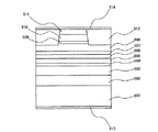
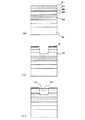
図1は、本発明の第1の実施例に係る半導体レーザの断面構造をあらわす概略図、図3は製造過程を示す模式図である。
【0021】
本実施例のレーザダイオードは以下のようなプロセスにより形成された。まず有機金属気相成長(MOCVD)法により、(0001)面方位(C面)を有するサファイア基板101上に、アンドープのGaNバッファ層102を20nmと、n型の導電型を有する(以下n−と記す)GaNコンタクト層103を5μmと、n−Al0.3Ga0.7Nクラッド層104を1μmと、n−GaN光閉じ込め層105を0.1μmと、InGaN系MQW構造による活性層106と、p型の導電型を有する(以下p−と記す)GaN光閉じ込め層107を0.1μmと、p−Al0.3Ga0.7Nクラッド層108を1μmと、p−GaNコンタクト層109を0.5μmと、を順次エピタキシャル成長させる(図3(A))。
【0022】
次に、p−コンタクト層109の一部にマスキングM1を施し、被マスク部以外のエピタキシャル層をn−コンタクト層103中の適当な深さまでドライエッチングし、メサ形状を形成する(図3(B))。
【0023】
更に、前記マスクを剥離後、メサ頂上の一部および前のエッチングにより露出したn−コンタクト層103面の全面をマスクM2により被覆し、再度ドライエッチングを施して、メサ上部にリッジ構造を形成する。このときエッチングの深さはp−クラッド層108中のいずれかの位置までとし、残し膜厚を制御する必要はない(図3(C))。
【0024】
続いて電子ビーム(EB)蒸着法により、TiO2とZrO2の混合物を素子上面から蒸着する。蒸着膜の厚さは、蒸着膜の表面がリッジ上面と同じ高さになる厚さとする。すなわち、TiO2とZrO2の混合物からなる埋込層110により、リッジ部を埋め込む(図3(D)。
【0025】
最後にマスクM2及びリッジ上のTiO2とZrO2の混合物、n−GaNコンタクト層103上に形成されているマスクM2及びマスクM2上のTiO2とZrO2の混合物を除去し、n−電極111及びp−電極112を形成し、図1のリッジ導波型レーザ構造が完成する。
【0026】
本実施例の半導体レーザでは、活性層106から発する光の波長は520nmとなるように設計した。この波長に対するp−クラッド層108の屈折率はおよそ2.33であるので、埋込層の誘電体は、TiO2(屈折率=2.35)とZrO2(屈折率=2.05)を混合物とし、蒸着された混合膜の波長520nmにおける屈折率が2.33になるように調整した。活性層の設計変更により発振波長が変化した場合にはp−クラッド層108の屈折率も変化するが、その時は埋込層もTiO2とZrO2の混合比を変更したり、あるいは蒸着条件を変えたりして屈折率を変化させればよい。また、誘電体の種類はTiO2やZrO2に限られるものではなく、レーザの発振波長に対して透明であればどのような誘電体が用いられてもよい。また誘電体膜の形成方法もEB蒸着法に限られるものでは勿論なく、スパッタリング法やその他の薄膜形成プロセスが用いられても構わない。
【0027】
以上のように形成された本実施例の埋め込みリッジ導波型半導体レーザでは、電流は絶縁体である誘電体埋込層110により狭窄され、リッジ部直下の活性層に集中するため、利得分布が生じる。一方、埋込層の屈折率はp−クラッド層のそれと等しいため、活性層で発した光は屈折率分布を感じない。したがって該レーザの横モード制御はリッジ幅の制御によりなされればよいので容易であり、またドライエッチングによるp−クラッド層108の残し膜厚を精密に制御する必要がないのでエッチング誤差の許容範囲が広がり、生産歩留まりが向上する。
【0028】
さらに、エッチングにより形成したリッジ状ストライプ部を、TiO2とZrO2の混合物からなる埋込層110により埋め込んだため、エッチング加工時に生じた損傷による結晶欠陥が、連続通電動作によっても活性層へ伝搬せず、動作寿命を格段に向上した素子が実現できた。
【0029】
図4は、本発明の第2の実施例に係る半導体レーザの断面構造をあらわす概略図である。本実施例のレーザダイオードは絶縁性基板を用いているため、その形成プロセスは実施例1とほぼ同様の加工工程を有する。まずMOCVD法により、(0001)面方位(C面)を有するサファイア基板401上に、アンドープのGaNバッファ層402を20nmと、n−GaNコンタクト層403を5μmと、n−Al0.08Ga0.92N第1クラッド層404を1μmと、n−GaN光閉じ込め層405を0.1μmと、InGaN系MQW構造による活性層406と、p−Al0.2Ga0.8N蒸発防止層407を0.05μmと、p−GaN光閉じ込め層408を0.1μmと、p−Al0.08Ga0.92N第2クラッド層409を0.2μmと、p−GaN光ガイド層410を0.05μmと、p−Al0.08Ga0.92N第3クラッド層411を0.8μmと、p−GaNコンタクト層412を0.5μmとを順次エピタキシャル成長させる。
【0030】
次に、p−コンタクト層412の一部にマスキングM1を施し、被マスク部以外のエピタキシャル層をn−コンタクト層403中の適当な深さまでドライエッチングし、メサ形状を形成する。更に、前記マスクM1を剥離後、メサ頂上の一部および前のエッチングにより露出したn−コンタクト層403面の全面をマスクM2により被覆し、再度ドライエッチングを施して、メサ上部にリッジ構造を形成する。このときエッチングの深さはp−第2クラッド層409中のいずれかの位置までとし、残し膜厚を制御する必要はない。続いて分子線エピタキシ(MBE)法により、ClドープZnMgSSe化合物を素子上面から成膜する。該化合物層の厚さは、層の表面がリッジ上面と同じ高さになる厚さとする。即ちZnMgSSeからなる埋込層413により、リッジ部を埋め込む。
【0031】
最後にマスクM1、マスクM2及びマスクM1、マスクM2上のClドープZnMgSSe化合物を除去し、n−電極414及びp−電極415を形成し、図4のリッジ導波型レーザ構造が完成する。本実施例の半導体レーザでは、活性層406から発する光の波長は410nmとなるように設計した。この波長に対するp−第2クラッド層409の屈折率はおよそ2.50であるので、埋込層のZnMgSSeの各元素の組成比はエネルギーギャップが3.03eV以上、屈折率は2.50となるように調節されている。活性層の設計変更により発振波長が変化した場合にはp−第2クラッド層409の屈折率も変化するが、その時は埋込層もZnMgSSeの組成比を変更して屈折率を変化させればよい。また、埋込に用いるII−VI族半導体の種類はZnMgSSeに限られるものではなく、たとえばZnCdSeなどが用いられてもよい。またII−VI族半導体膜の形成方法もMBE法によるエピタキシャル成長に限られるものでは勿論なく、スパッタリング法やその他の薄膜形成プロセスが用いられても構わない。
【0032】
以上のように形成された本実施例のリッジ導波型半導体レーザでは、電流はn型の導電型を示すClドープZnMgSSe埋込層413により狭窄され、リッジ部直下の活性層に集中するため、利得分布が生じる。一方、リッジ内部に形成された光ガイド層410は屈折率がp−第2クラッド層409及び埋込層413に対して大きく、またリッジ外では光ガイド層410が取り除かれているため、リッジ内外で実効的な屈折率に分布が生じる。したがって、光ガイド層を有さない第1の実施例に比べて、リッジ直下部への光り閉じ込めの効率がよくなり、横モード制御がより容易になる。またドライエッチングによるリッジ形成においては、エッチング底面が少なくとも光ガイド層410とp−第2クラッド層409の界面に達していればよく、光閉じ込め層408に達しなければオーバーエッチも許容されるので、残し膜厚を精密に制御する必要がなくなり、生産歩留まりが向上する。
【0033】
さらに、エッチングにより形成したリッジ状ストライプ部を、ZnMgSSeからなる埋込層413により埋め込んだため、エッチング加工時に生じた損傷による結晶欠陥が、連続通電動作によっても活性層へ伝搬せず、動作寿命を格段に向上した素子が実現できた。
【0034】
図5は、本発明の第3の実施例に係る半導体レーザの断面構造をあらわす概略図である。本実施例のレーザダイオードは以下のようなプロセスにより形成された。まずMOCVD法により、n−SiC基板501上に、アンドープのGaNバッファ層502を20nmと、n−Al0.08Ga0.92N第1クラッド層503を1μmと、n−GaN光閉じ込め層504を0.1μmと、InGaN系MQW構造による活性層505と、p−Al0.2Ga0.8N蒸発防止層506を0.05μmと、p−GaN光閉じ込め層507を0.1μmと、p−Al0.08Ga0.92N第2クラッド層508を0.2μmと、p−Al0.02Ga0.98N光ガイド層509を0.05μmと、p−Al0.08Ga0.92N第3クラッド層510を0.8μmと、p−GaNコンタクト層511を0.5μmとを順次エピタキシャル成長させる。次に、p−コンタクト層511の一部にマスクを施し、被マスク部以外のエピタキシャル層をドライエッチングして、リッジ構造を形成する。このときエッチングの深さはp−第2クラッド層508中のいずれかの位置までとし、残し膜厚を制御する必要はない。続いて、リッジ上部にマスクを残したままMOCVD法による選択成長により、n−Al0.08Ga0.92N層をリッジ側面にのみ成膜する。該AlGaN層の厚さは、層の表面がリッジ上面と同じ高さになる厚さとする。即ちn−Al0.08Ga0.92Nからなる埋込層512により、リッジ部を埋め込む。最後にマスクを除去し、基板裏面にn−電極513を、素子上面にp−電極514を形成し、図5のリッジ導波型レーザ構造が完成する。
【0035】
本実施例の半導体レーザでは、活性層505から発する光の波長は450nmとなるように設計した。この波長に対するp−第2クラッド層508の屈折率はおよそ2.45である。本実施例においては、埋込層512はp−第2クラッド層508と導電型が異なるだけで同一の組成であり、該埋込層の屈折率はおよそ2.45であり、発振波長に対して透明である。したがって本実施例のリッジ導波型半導体レーザでは、素子電流はn−AlGaN埋込層512により狭窄され、リッジ部直下の活性層に集中するため、利得分布が生じる。一方、リッジ内部に形成された光ガイド層509は屈折率がp−第2クラッド層508及び埋込層412に対して大きく、またリッジ外では光ガイド層410が取り除かれているため、リッジ内外で実効的な屈折率に分布が生じる。したがって第2の実施例と同様、リッジ直下部への光り閉じ込めの効率がよくなり、横モード制御がより容易になる。またドライエッチングによるリッジ形成においては、エッチング底面が少なくとも光ガイド層509とp−第2クラッド層508の界面に達していればよく、光閉じ込め層507に達しなければオーバーエッチも許容されるので、残し膜厚を精密に制御する必要がなくなり、生産歩留まりが向上する。
【0036】
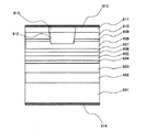
図6は、本発明の第4の実施例に係る半導体レーザの断面構造をあらわす概略図、図7は製造過程を示す模式図である。
【0037】
本実施例のレーザダイオードは以下のようなプロセスにより形成された。まずMOCVD法により、n−GaN基板601上に、アンドープのGaNバッファ層602を20nmと、n−Al0.08Ga0.92N第1クラッド層603を1μmと、n−GaN光閉じ込め層604を0.1μmと、InGaN系MQW構造による活性層605と、p−Al0.2Ga0.8N蒸発防止層606を0.05μmと、p−GaN光閉じ込め層607を0.1μmと、p−Al0.08Ga0.92N第2クラッド層608を0.2μmと、n−Al0.3Ga0.7N光反射層609を0.1μmと、p−Al0.08Ga0.92N第3クラッド層610を0.7μmと、p−GaNコンタクト層611を0.5μmと、を順次エピタキシャル成長させる(図7(A))。
【0038】
次に、p−コンタクト層611の一部にマスキングM1を施し、被マスク部以外のエピタキシャル層をドライエッチングして、凹構造を形成する。このときエッチングの深さはp−第2クラッド層608中のいずれかの位置までとし、残し膜厚を制御する必要はない(図7(B))。
【0039】
続いて、凹部以外のマスクを残したままMOCVD法による選択成長により、凹構造の溝内部にのみ選択的にp−Al0.08Ga0.92N層612をp−第3クラッド層610とp−コンタクト層611の界面付近まで、続いてp−GaN層613をp−コンタクト層611の表面近傍までエピタキシャル成長させる。即ちp−Al0.08Ga0.92Nからなる埋込層612により、凹構造の溝部を埋め込む(図7(C))。
【0040】
最後にマスクM1を除去し、基板裏面にn−電極614を、素子上面にp−電極615を形成し、図6のレーザ構造が完成する。本実施例の半導体レーザでは、活性層605から発する光の波長は430nmとなるように設計した。本実施例においては、埋込層612はp−第2クラッド層608と導電型も組成も同一であり、かつ凹構造の溝部分以外に付設されている光反射層609はその導電型の違いから電流阻止層となるため、素子電流は溝部直下の活性層に集中し、レーザの横方向に対して利得分布が生じる。一方、溝部以外に付設されている光反射層609は屈折率がp−第2クラッド層608及び埋込層612に対して小さく、また溝部では屈折率が一様であるので、溝部以外で光が感じる実効的な屈折率が小さいため、ストライプ構造の内外で実効屈折率に分布が生じる。したがって、ストライプ部への光り閉じ込めの効率がよくなり、横モード制御がより容易になる。またドライエッチングによる溝構造形成においては、エッチング底面が少なくとも光反射層609とp−第2クラッド層608の界面に達していればよく、光閉じ込め層607に達しなければオーバーエッチも許容されるので、残し膜厚を精密に制御する必要がなくなり、生産歩留まりが向上する。なお、上記の4実施例では種々の基板やバッファ層、光閉じ込め層など、請求の範囲にない構造が用いられているが、これらは特性のよいレーザ素子の形成のために用いられたものであって、リッジ部分の構造に関する本発明の実施に影響を及ぼすものではない。
【0041】
【発明の効果】
本発明によれば、従来のようにエッチングの残し膜厚によるリッジ導波型半導体レーザの横モード制御を行わないので、単一横モード特性を有する半導体レーザを高い生産歩留まりで作製することができる。
【図面の簡単な説明】
【図1】本発明の第1の実施例に係る半導体レーザの断面構造を示す模式図である。
【図2】従来の半導体レーザの断面構造を示す模式図である。
【図3】本発明の第1の実施例の半導体レーザの製作過程を示す模式図である。
【図4】本発明の第2の実施例に係る半導体レーザの断面構造を示す模式図である。
【図5】本発明の第3の実施例に係る半導体レーザの断面構造を示す模式図である。
【図6】本発明の第4の実施例に係る半導体レーザの断面構造を示す模式図である。
【図7】本発明の第4の実施例の半導体レーザの製作過程を示す模式図である。
【図8】従来の半導体レーザの室温・連続通電時の動作電流の変化を示す図である。
【図9】本発明の第1の実施例に係る半導体レーザの室温・連続通電時の動作電流の変化を示す図である。
【図10】光ガイド層の無い素子構造における、p−クラッド層残し膜厚とストライプ内外の実効屈折率差を従来例、本発明を比較して示す図である。
【図11】光ガイド層の有る素子構造における、p−クラッド層残し膜厚とストライプ内外の実効屈折率差を従来例、本発明を比較して示す図である。
【符号の説明】
101、401 サファイア基板
103、403 n−GaNコンタクト層
104 n−Al0.15Ga0.85Nクラッド層
105、405、504、604 n−GaN光閉じ込め層
106、406、505、605 InGaN系多重量子井戸活性層
107、408、507、607 p−GaN光閉じ込め層
108 p−Al0.15Ga0.85Nクラッド層
109、412、511、611 p−GaNコンタクト層
110 誘電体埋込層
404、503、603 n−Al0.08Ga0.92N第1クラッド層
407、506、606 p−Al0.2Ga0.8N蒸発防止層
409、508、608 p−Al0.08Ga0.92N第2クラッド層
410、509、609 p−GaN光ガイド層
411、510、610 p−Al0.08Ga0.92N第3クラッド層
413 ClドープZnMgSSe埋込層
501 n−SiC基板
512 n−Al0.08Ga0.92N埋込層
601 n−GaN基板
612 p−Al0.08Ga0.92N埋込層
613 p−GaN層[0001]
BACKGROUND OF THE INVENTION
The present invention relates to a semiconductor laser made of a semiconductor laser group III nitride semiconductor.
[0002]
[Prior art]
FIG. 2 is a schematic cross-sectional view showing a conventional ridge waveguide type III-nitride semiconductor laser. 2 includes a
[0003]
FIG. 10 shows a device structure having no optical guide layer, a p-cladding layer remaining film thickness, an effective refractive index difference between the inside and outside of the stripe (conventional example), and an etching portion made of a material having the same refractive index as that of the p-cladding layer. It is a figure which shows the comparison of the effective refractive index difference (invention) inside and outside a stripe at the time of embedding. In the conventional ridge waveguide type III-nitride semiconductor laser, as shown in FIG. 10, the difference in refractive index due to the difference in the thickness of the p-
[0004]
Thereby, the optical characteristics of the vertical light emission angle = 34 ° and the horizontal light emission angle = 7 ° are obtained by continuous energization at room temperature. In addition, the element lifetime at room temperature and continuous energization is about 35 hours. FIG. 8 shows this, and shows a change in operating current of a conventional ridge waveguide type III-nitride semiconductor laser at room temperature / continuous energization.
[0005]
[Problems to be solved by the present invention]
However, the conventional ridge waveguide type III-nitride semiconductor laser as shown in FIG. 2 has a problem that it is extremely difficult to manufacture a semiconductor laser having uniform transverse mode characteristics with a high yield. This is because, since there is no appropriate chemical etching solution for the group III nitride semiconductor, dry etching such as RIE or RIBE is used for etching, but there is no appropriate etch stop layer. ) Part of the p-
[0006]
A further problem is that the element lifetime at room temperature and continuous energization is short. This is because dry etching is used as a processing method for forming a stripe-shaped ridge shape, and therefore, the side surface and bottom surface of the etched semiconductor layer are damaged, resulting in crystal defects, and the ridge side surface and the outside of the ridge. The p-AlGaN cladding layer is covered with a SiO 2 protective film, but there are many pinholes in SiO 2 and the cause is that the crystal plane cannot be sufficiently protected. Confirmed.
[0007]
[Means for Solving the Problems]
In order to solve the above problems, the present invention provides an element structure in which the transverse mode does not change with respect to the change in the etching amount, and efficiently produces a ridge waveguide type III-nitride semiconductor laser with uniform characteristics. Make it possible to produce.
[0008]
Furthermore, by forming a dielectric layer with few pinholes outside the ridge-shaped stripe formed by etching, or a structure in which the semiconductor layer is formed thick and burying the ridge-shaped stripe substantially, crystal defects due to damage caused during the etching process are eliminated. Thus, an element that does not propagate to the active layer even by a continuous energization operation and whose operating life is significantly improved is realized.
[0009]
Alternatively, even if a concave groove formed by etching is used as a current path or a structure embedded in a semiconductor layer, crystal defects due to damage caused during etching processing do not propagate to the active layer even by continuous energization operation. , To achieve an element with a significantly improved operating life.
[0010]
That is, the semiconductor laser according to the present invention includes a first cladding layer having a first conductivity type, an active layer, a second cladding layer having a second conductivity type, and a contact layer having a second conductivity type on a substrate. And a structure in which only the upper part of the second cladding layer or the upper part of the second cladding layer or the contact layer is formed in a ridge shape in a part of the structure above the active layer, and is formed on both sides of the ridge part. The buried layer having the insulating or first conductivity type is transparent to the oscillation wavelength of the laser and has approximately the same refractive index as the second cladding layer,
The buried layer contains at least one of TiO 2 , ZrO 2 , HfO 2 , CeO 2 , In 2 O 3 , Nd 2 O 3 , Sb 2 O 3 , SnO 2 , Ta 2 O 5 , and ZnO. It is characterized by being a dielectric,
Alternatively, the buried layer is a ZnMgCdSSe compound semiconductor,
Alternatively, the buried layer is a semiconductor having substantially the same composition as the second cladding layer.
[0011]
By adopting the above-described structure, as shown in FIG. 10, the difference in refractive index between the inside and outside of the ridge portion is eliminated. On the other hand, the current confinement effect of the buried ridge layer causes a gain difference between the active layer immediately below the ridge and directly below the buried layer, and as a result, the transverse mode is controlled. In this structure, the error tolerance range with respect to the etching depth of the etching process for forming the ridge is wide, the lateral mode controllability is stabilized, and the production yield of laser devices with uniform characteristics is improved.
[0012]
In addition, since these embedding materials are transparent to the oscillation wavelength of the laser, there is no heat generation due to light absorption, and since the refractive index is substantially the same as that of the second cladding layer, it does not affect the transverse mode of the laser and is embedded. Suitable as a layer. Further, since the ridge-shaped stripe portion formed by etching is embedded in the buried layer, crystal defects due to damage caused during etching processing are not propagated to the active layer even by continuous energization operation, and the operating life is remarkably improved. Realize the element. Further, when a group III nitride semiconductor having substantially the same composition as the second cladding layer is used as the material of the buried layer, the lattice constant difference between the buried layer and the other epitaxial layer is eliminated. It is possible to avoid the influence of stress such as thermal strain on the element.
[0013]
According to another aspect of the semiconductor laser of the present invention, a first cladding layer having a first conductivity type, an active layer, a second cladding layer having a second conductivity type, and a second conductivity are formed on a substrate. A light guide layer having a mold and a higher refractive index than the second cladding layer, a third cladding layer having the second conductivity type, and a contact layer having the second conductivity type, and A part of the structure above the active layer, in which the arbitrary position in the second cladding layer to the third cladding layer, or the arbitrary position in the second cladding layer or the contact layer is formed in a ridge shape, and the ridge portion The buried layer having insulating or first conductivity type formed on both sides of the substrate is transparent to the oscillation wavelength of the laser and has substantially the same refractive index as that of the second cladding layer,
The light guide layer is made of InGaAlN,
Alternatively, the buried layer is at least one of TiO 2 , ZrO 2 , HfO 2 , CeO 2 , In 2 O 3 , Nd 2 O 3 , Sb 2 O 3 , SnO 2 , Ta 2 O 5 and ZnO. A dielectric film containing
Alternatively, the buried layer is a ZnMgCdSSe compound semiconductor,
Alternatively, the buried layer is a semiconductor having substantially the same composition as the second cladding layer.
[0014]
FIG. 11 shows a material structure having an optical guide layer having a p-cladding layer remaining film thickness, a difference in effective refractive index inside and outside the stripe (conventional example), and a material having the same refractive index as that of the p-cladding layer in the etched portion. FIG. 11 is a view showing a comparison of the effective refractive index difference (invention) inside and outside the stripe when embedded, and is shown in FIG. 11 by adopting a structure in which the light guide layer is included in the ridge portion as described above. Thus, the effective refractive index inside the ridge is increased, so that the lateral light distribution field is more concentrated in the center, and the transverse mode control is more effective than the ridge waveguide laser using the gain difference. It becomes easy. When there is no buried layer or the refractive index of the buried layer is different from that of the second cladding layer, the thickness of the second cladding layer outside the ridge (remaining etching thickness) is the value of the effective refractive index outside the ridge. It greatly affects the laser characteristics.
[0015]
However, in the structure according to the present invention, since the refractive index of the buried layer is the same as that of the second cladding layer, the thickness of the second cladding layer outside the ridge (the film thickness remaining after etching) affects the effective refractive index outside the ridge. Therefore, it is not necessary to precisely control the etching depth, and the etching depth only needs to reach the interface between the light guide layer and the second cladding layer so that the light guide layer exists inside the ridge. In addition, even if overetching is performed, the bottom surface of the etching only needs to be inside the second cladding layer, so that an error tolerance during etching is large, the lateral mode controllability is stabilized, and the laser production yield is improved.
[0016]
According to still another aspect of the present invention, there is provided a semiconductor laser comprising: a first clad layer having a first conductivity type; an active layer; a second clad layer having a second conductivity type; A light reflecting layer having a first conductivity type and a lower refractive index than the second cladding layer, a third cladding layer having the second conductivity type, and a contact layer having the second conductivity type are laminated. And an arbitrary position in the second cladding layer to the third cladding layer, or an arbitrary position in the second cladding layer or the contact layer in a part of the structure above the active layer is formed in a concave shape. The buried layer formed inside the recess has a second conductivity type and is a semiconductor having substantially the same composition as the second cladding layer,
The light reflecting layer is made of InGaAlN.
[0017]
As described above, by taking a structure in which a semiconductor layer having an insulating property or a first conductivity type and having a refractive index lower than that of the second cladding layer is included in a portion other than the groove of the concave structure, the device current is It concentrates on the groove part of the concave structure, and gain distribution is generated in the lateral direction of the laser. Further, the effective refractive index is relatively larger in the groove part of the concave structure than other parts, The light distribution field in the direction is more concentrated in the center, and the transverse mode control of the laser becomes easy in combination with the effect of the gain distribution.
[0018]
Further, by using InGaAlN as the material of the semiconductor layer having a lower refractive index than the second cladding layer stacked on the second cladding layer, each group III nitride layer continuously grown on the layer is Epitaxial growth is possible while suppressing the occurrence of defects, leading to improved laser reliability.
[0019]
DETAILED DESCRIPTION OF THE INVENTION
Embodiments of the present invention will be described below with reference to the drawings.
[0020]
FIG. 1 is a schematic view showing a cross-sectional structure of a semiconductor laser according to a first embodiment of the present invention, and FIG. 3 is a schematic view showing a manufacturing process.
[0021]
The laser diode of this example was formed by the following process. First, an undoped
[0022]
Next, masking M1 is applied to a part of the p-
[0023]
Further, after removing the mask, a part of the top of the mesa and the entire surface of the n-
[0024]
Subsequently, a mixture of TiO 2 and ZrO 2 is deposited from the upper surface of the device by an electron beam (EB) deposition method. The thickness of the vapor deposition film is set so that the surface of the vapor deposition film is the same height as the top surface of the ridge. That is, the ridge portion is buried with the buried
[0025]
Finally, remove the mask M2 and TiO 2 and mixtures of ZrO 2 on the ridge, a mixture of n-
[0026]
In the semiconductor laser of this example, the wavelength of light emitted from the
[0027]
In the buried ridge waveguide semiconductor laser of the present embodiment formed as described above, the current is narrowed by the dielectric buried
[0028]
Further, since the ridge-shaped stripe portion formed by etching is buried with the buried
[0029]
FIG. 4 is a schematic view showing a cross-sectional structure of a semiconductor laser according to the second embodiment of the present invention. Since the laser diode of this embodiment uses an insulating substrate, the formation process has almost the same processing steps as those of the first embodiment. First, by MOCVD, on the
[0030]
Next, a part of the p-
[0031]
Finally, the mask M1, the mask M2, the mask M1, and the Cl-doped ZnMgSSe compound on the mask M2 are removed to form the n-
[0032]
In the ridge waveguide semiconductor laser of this embodiment formed as described above, the current is confined by the Cl-doped ZnMgSSe buried
[0033]
Furthermore, since the ridge-shaped stripe portion formed by etching is buried with the buried
[0034]
FIG. 5 is a schematic view showing a cross-sectional structure of a semiconductor laser according to the third embodiment of the present invention. The laser diode of this example was formed by the following process. First, by MOCVD, an undoped
[0035]
In the semiconductor laser of this example, the wavelength of light emitted from the
[0036]
FIG. 6 is a schematic view showing a cross-sectional structure of a semiconductor laser according to a fourth embodiment of the present invention, and FIG. 7 is a schematic view showing a manufacturing process.
[0037]
The laser diode of this example was formed by the following process. First, by MOCVD, on the n-
[0038]
Next, a mask M1 is applied to a part of the p-
[0039]
Subsequently, the p-Al 0.08 Ga 0.92 N layer 612 is selectively formed only in the groove of the concave structure by the selective growth by the MOCVD method while leaving the mask other than the concave portion, and the p-
[0040]
Finally, the mask M1 is removed, an n-
[0041]
【The invention's effect】
According to the present invention, since the lateral mode control of the ridge waveguide semiconductor laser is not performed by the remaining etching film thickness as in the prior art, a semiconductor laser having a single lateral mode characteristic can be manufactured with a high production yield. .
[Brief description of the drawings]
FIG. 1 is a schematic diagram showing a cross-sectional structure of a semiconductor laser according to a first embodiment of the present invention.
FIG. 2 is a schematic view showing a cross-sectional structure of a conventional semiconductor laser.
FIG. 3 is a schematic view showing a manufacturing process of the semiconductor laser according to the first embodiment of the present invention.
FIG. 4 is a schematic diagram showing a cross-sectional structure of a semiconductor laser according to a second example of the present invention.
FIG. 5 is a schematic diagram showing a cross-sectional structure of a semiconductor laser according to a third example of the present invention.
FIG. 6 is a schematic diagram showing a cross-sectional structure of a semiconductor laser according to a fourth example of the present invention.
FIG. 7 is a schematic view showing a manufacturing process of a semiconductor laser according to a fourth embodiment of the present invention.
FIG. 8 is a diagram showing a change in operating current when a conventional semiconductor laser is continuously energized at room temperature.
FIG. 9 is a diagram showing a change in operating current during continuous energization of the semiconductor laser according to the first embodiment of the present invention.
FIG. 10 is a diagram showing a p-cladding layer remaining film thickness and an effective refractive index difference between the inside and outside of a stripe in a device structure without a light guide layer in comparison with a conventional example and the present invention.
FIG. 11 is a diagram showing a p-cladding layer remaining film thickness and an effective refractive index difference between the inside and outside of a stripe in a device structure having a light guide layer in comparison with a conventional example and the present invention.
[Explanation of symbols]
101, 401 sapphire substrate 103,403 n-GaN contact layer 104 n-Al 0.15 Ga 0.85 N cladding layer 105,405,504,604 n-GaN light confining layer 106,406,505,605 InGaN-based multi-quantum well
Claims (11)
前記埋込層が、TiO2、ZrO2、HfO2、CeO2、In2O3、Nd2O3、Sb2O3、SnO2、Ta2O5、ZnOのうち少なくとも1種類以上を含む誘電体膜であることを特徴とする化合物半導体レーザ。In a semiconductor laser made of a group III nitride semiconductor, a first cladding layer having a first conductivity type, an active layer, and a second cladding layer having a second conductivity type are stacked in this order on a substrate. In addition, the upper part of the second cladding layer is formed in a ridge shape in a part of the structure above the active layer, and has an insulating or first conductivity type formed on both sides of the ridge portion. The layer is transparent to the lasing wavelength of the laser and has the same refractive index as the second cladding layer;
The buried layer contains at least one of TiO 2 , ZrO 2 , HfO 2 , CeO 2 , In 2 O 3 , Nd 2 O 3 , Sb 2 O 3 , SnO 2 , Ta 2 O 5 , and ZnO. A compound semiconductor laser comprising a dielectric film.
前記埋込層が、ZnMgCdSSe化合物半導体であることを特徴とする化合物半導体レーザ。In a semiconductor laser made of a group III nitride semiconductor, a first cladding layer having a first conductivity type, an active layer, and a second cladding layer having a second conductivity type are stacked in this order on a substrate. And an upper portion of the second cladding layer is formed in a ridge shape in a part of the structure above the active layer, and embedded layers having a first conductivity type are formed on both sides of the ridge portion , The buried layer is transparent to the laser oscillation wavelength and has the same refractive index as the second cladding layer;
A compound semiconductor laser, wherein the buried layer is a ZnMgCdSSe compound semiconductor.
前記活性層上方の一部において前記第2クラッド層内の任意の位置ないし前記第3クラッド層には、リッジ構造が設けられており、
該リッジ構造は、第1の導電型を有する埋込層により挟まれており、
該埋込層は、前記第2クラッド層と同組成のIII族窒化物半導体からなることを特徴とする化合物半導体レーザ。A first clad layer having a first conductivity type and made of a group III nitride semiconductor, an active layer made of a group III nitride semiconductor, and a group III nitride semiconductor having a second conductivity type on a substrate. A second cladding layer, a light guide layer having a second conductivity type and a higher refractive index than the second cladding layer, and a third cladding layer having the second conductivity type are laminated in this order. And
A ridge structure is provided in an arbitrary position in the second cladding layer in the part above the active layer or in the third cladding layer,
The ridge structure is sandwiched between buried layers having the first conductivity type ,
The compound semiconductor laser, wherein the buried layer is made of a group III nitride semiconductor having the same composition as the second cladding layer.
Priority Applications (12)
| Application Number | Priority Date | Filing Date | Title |
|---|---|---|---|
| JP07477997A JP3897186B2 (en) | 1997-03-27 | 1997-03-27 | Compound semiconductor laser |
| EP04009210A EP1437809B1 (en) | 1997-03-27 | 1998-03-25 | Compound semiconductor laser |
| US09/402,135 US6597716B1 (en) | 1997-03-27 | 1998-03-25 | Compound semiconductor laser |
| DE1998624162 DE69824162T2 (en) | 1997-03-27 | 1998-03-25 | COMPOUND SEMICONDUCTOR LASER |
| DE69836698T DE69836698T2 (en) | 1997-03-27 | 1998-03-25 | Compound semiconductor laser |
| EP06023105A EP1744419B1 (en) | 1997-03-27 | 1998-03-25 | Compound semiconductor laser |
| DE69841813T DE69841813D1 (en) | 1997-03-27 | 1998-03-25 | Compound semiconductor laser |
| PCT/JP1998/001308 WO1998044606A1 (en) | 1997-03-27 | 1998-03-25 | Compound semiconductor laser |
| KR1019997008790A KR100362862B1 (en) | 1997-03-27 | 1998-03-25 | Compound semiconductor laser |
| EP98910983A EP0971465B1 (en) | 1997-03-27 | 1998-03-25 | Compound semiconductor laser |
| US10/465,164 US6855570B2 (en) | 1997-03-27 | 2003-06-18 | Compound semiconductor laser |
| US10/993,563 US7042011B2 (en) | 1997-03-27 | 2004-11-18 | Compound semiconductor laser |
Applications Claiming Priority (1)
| Application Number | Priority Date | Filing Date | Title |
|---|---|---|---|
| JP07477997A JP3897186B2 (en) | 1997-03-27 | 1997-03-27 | Compound semiconductor laser |
Related Child Applications (2)
| Application Number | Title | Priority Date | Filing Date |
|---|---|---|---|
| JP2006300411A Division JP3950473B2 (en) | 2006-11-06 | 2006-11-06 | Compound semiconductor laser |
| JP2006313600A Division JP2007043215A (en) | 2006-11-20 | 2006-11-20 | Compound semiconductor laser |
Publications (2)
| Publication Number | Publication Date |
|---|---|
| JPH10270792A JPH10270792A (en) | 1998-10-09 |
| JP3897186B2 true JP3897186B2 (en) | 2007-03-22 |
Family
ID=13557128
Family Applications (1)
| Application Number | Title | Priority Date | Filing Date |
|---|---|---|---|
| JP07477997A Expired - Fee Related JP3897186B2 (en) | 1997-03-27 | 1997-03-27 | Compound semiconductor laser |
Country Status (6)
| Country | Link |
|---|---|
| US (3) | US6597716B1 (en) |
| EP (3) | EP1744419B1 (en) |
| JP (1) | JP3897186B2 (en) |
| KR (1) | KR100362862B1 (en) |
| DE (3) | DE69841813D1 (en) |
| WO (1) | WO1998044606A1 (en) |
Families Citing this family (31)
| Publication number | Priority date | Publication date | Assignee | Title |
|---|---|---|---|---|
| WO2000052796A1 (en) * | 1999-03-04 | 2000-09-08 | Nichia Corporation | Nitride semiconductor laser element |
| JP4991025B2 (en) * | 1999-06-10 | 2012-08-01 | 日亜化学工業株式会社 | Nitride semiconductor laser device |
| US6738403B2 (en) * | 2000-04-06 | 2004-05-18 | Fuji Photo Film Co., Ltd. | Semiconductor laser element and semiconductor laser |
| JP4251529B2 (en) | 2001-02-14 | 2009-04-08 | シャープ株式会社 | Nitride semiconductor laser device and optical information reproducing apparatus using the same |
| US6822272B2 (en) * | 2001-07-09 | 2004-11-23 | Nichia Corporation | Multilayered reflective membrane and gallium nitride-based light emitting element |
| US7067849B2 (en) | 2001-07-17 | 2006-06-27 | Lg Electronics Inc. | Diode having high brightness and method thereof |
| US6949395B2 (en) | 2001-10-22 | 2005-09-27 | Oriol, Inc. | Method of making diode having reflective layer |
| US7148520B2 (en) | 2001-10-26 | 2006-12-12 | Lg Electronics Inc. | Diode having vertical structure and method of manufacturing the same |
| KR20030038125A (en) * | 2001-11-08 | 2003-05-16 | 엘지전자 주식회사 | Semiconductor laser diode |
| KR100437786B1 (en) * | 2001-11-09 | 2004-06-30 | 엘지전자 주식회사 | Semiconductor Laser Diode |
| JP4015865B2 (en) * | 2002-03-22 | 2007-11-28 | 松下電器産業株式会社 | Manufacturing method of semiconductor device |
| JP4615179B2 (en) * | 2002-06-27 | 2011-01-19 | 古河電気工業株式会社 | Semiconductor laser device, semiconductor laser module, and optical fiber amplifier |
| JP4067928B2 (en) * | 2002-09-27 | 2008-03-26 | 株式会社東芝 | Method for manufacturing gallium nitride compound semiconductor device and method for processing gallium nitride compound semiconductor layer |
| KR100523484B1 (en) * | 2002-11-11 | 2005-10-24 | 한국전자통신연구원 | Method for fabricating semiconductor optical devices having current-confined structure |
| DE60311678T2 (en) * | 2002-12-20 | 2007-11-22 | Cree, Inc. | METHOD FOR PRODUCING SEMICONDUCTOR DEVICES WITH MESASTRUCTURES AND MULTIPLE PASSIVATION LAYERS AND RELATED DEVICES |
| DE10261676A1 (en) * | 2002-12-31 | 2004-07-22 | Osram Opto Semiconductors Gmbh | Light emitting diode chip comprises epitaxial semiconductor sequence having protective layer and electromagnetic radiation emitting active zone, used for high efficiency semiconductor light emitting diodes |
| KR20050042715A (en) * | 2003-11-04 | 2005-05-10 | 삼성전자주식회사 | Electrode structure, semiconductor light-emitting device provided with the same and method for manufacturing the same |
| US7791061B2 (en) * | 2004-05-18 | 2010-09-07 | Cree, Inc. | External extraction light emitting diode based upon crystallographic faceted surfaces |
| KR100818522B1 (en) * | 2004-08-31 | 2008-03-31 | 삼성전기주식회사 | The fabrication method of laser diode |
| JP2007115877A (en) * | 2005-10-20 | 2007-05-10 | Fujifilm Corp | Solid laser device |
| US7440482B2 (en) | 2005-11-01 | 2008-10-21 | Nichia Corporation | Nitride semiconductor laser element and method for manufacturing the same |
| KR100774458B1 (en) * | 2006-02-27 | 2007-11-08 | 엘지전자 주식회사 | Semiconductor laser device and method for manufacturing the same |
| JP4940987B2 (en) | 2006-03-20 | 2012-05-30 | 日亜化学工業株式会社 | Nitride semiconductor laser device and manufacturing method thereof |
| US7773650B2 (en) | 2006-12-28 | 2010-08-10 | Nichia Corporation | Nitride semiconductor laser element |
| JP2007184644A (en) * | 2007-04-02 | 2007-07-19 | Matsushita Electric Ind Co Ltd | Semiconductor device and method of manufacturing same |
| US7615389B2 (en) * | 2007-05-31 | 2009-11-10 | Corning Incorporated | GaN lasers on ALN substrates and methods of fabrication |
| US8373152B2 (en) * | 2008-03-27 | 2013-02-12 | Lg Innotek Co., Ltd. | Light-emitting element and a production method therefor |
| JP5735216B2 (en) | 2009-02-27 | 2015-06-17 | 日亜化学工業株式会社 | Nitride semiconductor laser device |
| JP2011009610A (en) * | 2009-06-29 | 2011-01-13 | Sharp Corp | Nitride semiconductor laser device and wafer |
| US8896008B2 (en) | 2013-04-23 | 2014-11-25 | Cree, Inc. | Light emitting diodes having group III nitride surface features defined by a mask and crystal planes |
| KR20220032917A (en) * | 2020-09-08 | 2022-03-15 | 삼성전자주식회사 | Micro light emitting device and display apparatus having the same |
Family Cites Families (18)
| Publication number | Priority date | Publication date | Assignee | Title |
|---|---|---|---|---|
| JPS6085585A (en) * | 1983-10-17 | 1985-05-15 | Nec Corp | Buried type semiconductor laser |
| JPH067618B2 (en) | 1983-12-26 | 1994-01-26 | 株式会社東芝 | Semiconductor laser device |
| JPS63166285A (en) * | 1986-12-26 | 1988-07-09 | Toshiba Corp | Semiconductor light-emitting device and manufacture thereof |
| JP3015371B2 (en) | 1988-01-20 | 2000-03-06 | 株式会社東芝 | Semiconductor laser |
| JPH053376A (en) | 1990-09-28 | 1993-01-08 | Seiko Epson Corp | Manufacture of semiconductor laser |
| JP3116675B2 (en) * | 1993-07-28 | 2000-12-11 | ソニー株式会社 | Semiconductor laser |
| JPH07235723A (en) | 1994-02-23 | 1995-09-05 | Hitachi Ltd | Semiconductor laser element |
| JPH0818159A (en) | 1994-04-25 | 1996-01-19 | Hitachi Ltd | Semiconductor laser element and fabrication thereof |
| JPH0856055A (en) | 1994-08-11 | 1996-02-27 | Hitachi Ltd | Semiconductor laser system |
| JPH0897507A (en) * | 1994-09-29 | 1996-04-12 | Rohm Co Ltd | Semiconductor laser |
| JP3432910B2 (en) * | 1994-09-28 | 2003-08-04 | ローム株式会社 | Semiconductor laser |
| EP0918384B1 (en) * | 1995-01-20 | 2002-12-11 | Matsushita Electric Industrial Co., Ltd. | Semiconductor light emitting device and method for fabricating the same |
| JPH08204285A (en) * | 1995-01-26 | 1996-08-09 | Nec Corp | Semiconductor laser and its manufacture |
| US5742629A (en) * | 1995-07-21 | 1998-04-21 | Matsushita Electric Industrial Co., Ltd. | Semiconductor laser and production method thereof |
| JPH09106946A (en) * | 1995-10-11 | 1997-04-22 | Mitsubishi Electric Corp | Semiconductor device, semiconductor laser and high-electron mobility transistor device |
| JPH09270569A (en) | 1996-01-25 | 1997-10-14 | Matsushita Electric Ind Co Ltd | Semiconductor laser device |
| US6055255A (en) * | 1996-02-01 | 2000-04-25 | Sharp Kabushiki Kaisha | Semiconductor laser device and method for producing the same |
| US5812576A (en) * | 1996-08-26 | 1998-09-22 | Xerox Corporation | Loss-guided semiconductor lasers |
-
1997
- 1997-03-27 JP JP07477997A patent/JP3897186B2/en not_active Expired - Fee Related
-
1998
- 1998-03-25 EP EP06023105A patent/EP1744419B1/en not_active Expired - Lifetime
- 1998-03-25 EP EP04009210A patent/EP1437809B1/en not_active Expired - Lifetime
- 1998-03-25 DE DE69841813T patent/DE69841813D1/en not_active Expired - Lifetime
- 1998-03-25 DE DE1998624162 patent/DE69824162T2/en not_active Expired - Lifetime
- 1998-03-25 EP EP98910983A patent/EP0971465B1/en not_active Expired - Lifetime
- 1998-03-25 KR KR1019997008790A patent/KR100362862B1/en not_active IP Right Cessation
- 1998-03-25 WO PCT/JP1998/001308 patent/WO1998044606A1/en active IP Right Grant
- 1998-03-25 DE DE69836698T patent/DE69836698T2/en not_active Expired - Lifetime
- 1998-03-25 US US09/402,135 patent/US6597716B1/en not_active Expired - Lifetime
-
2003
- 2003-06-18 US US10/465,164 patent/US6855570B2/en not_active Expired - Lifetime
-
2004
- 2004-11-18 US US10/993,563 patent/US7042011B2/en not_active Expired - Lifetime
Also Published As
| Publication number | Publication date |
|---|---|
| US20030206567A1 (en) | 2003-11-06 |
| EP1744419B1 (en) | 2010-08-04 |
| US7042011B2 (en) | 2006-05-09 |
| DE69836698T2 (en) | 2007-10-31 |
| DE69824162T2 (en) | 2004-11-18 |
| DE69824162D1 (en) | 2004-07-01 |
| KR100362862B1 (en) | 2002-12-11 |
| US6855570B2 (en) | 2005-02-15 |
| EP1744419A3 (en) | 2007-04-04 |
| EP0971465A1 (en) | 2000-01-12 |
| US6597716B1 (en) | 2003-07-22 |
| DE69836698D1 (en) | 2007-02-01 |
| DE69841813D1 (en) | 2010-09-16 |
| EP0971465A4 (en) | 2000-09-13 |
| US20050135447A1 (en) | 2005-06-23 |
| EP0971465B1 (en) | 2004-05-26 |
| JPH10270792A (en) | 1998-10-09 |
| EP1437809B1 (en) | 2006-12-20 |
| EP1437809A1 (en) | 2004-07-14 |
| WO1998044606A1 (en) | 1998-10-08 |
| EP1744419A2 (en) | 2007-01-17 |
| KR20010005722A (en) | 2001-01-15 |
Similar Documents
| Publication | Publication Date | Title |
|---|---|---|
| JP3897186B2 (en) | Compound semiconductor laser | |
| KR100763829B1 (en) | Semiconductor laser device, and method of manufacturing the same | |
| JP5028640B2 (en) | Nitride semiconductor laser device | |
| JP3060973B2 (en) | Manufacturing method of gallium nitride based semiconductor laser using selective growth method and gallium nitride based semiconductor laser | |
| JP2004289157A (en) | Laser diode structure and manufacturing method thereof | |
| JP2002016312A (en) | Nitride semiconductor element and its manufacturing method | |
| JP2000164987A (en) | Semiconductor light emitting element and manufacture thereof | |
| JPH07162086A (en) | Manufacture of semiconductor laser | |
| JP2000058981A (en) | Gallium nitride based semiconductor light emitting element and fabrication thereof | |
| JP4111696B2 (en) | Nitride semiconductor laser device | |
| JP2001057459A (en) | Semiconductor laser | |
| JP3918258B2 (en) | Semiconductor light emitting device and manufacturing method thereof | |
| JP3950473B2 (en) | Compound semiconductor laser | |
| JP3918259B2 (en) | Semiconductor light emitting device and manufacturing method thereof | |
| JPH10326940A (en) | Semiconductor light-emitting element | |
| JP2007043215A (en) | Compound semiconductor laser | |
| JP4497606B2 (en) | Semiconductor laser device | |
| JP2004014818A (en) | Semiconductor laser device | |
| JP2000091696A (en) | Semiconductor element, semiconductor light-emitting element and manufacture thereof | |
| JP2010021491A (en) | Nitride-based semiconductor laser element and method of manufacturing the same | |
| JPH09275239A (en) | Semiconductor laser device | |
| JP3820826B2 (en) | Semiconductor light emitting device and method for manufacturing semiconductor device | |
| JP2500588B2 (en) | Semiconductor laser and manufacturing method thereof | |
| JP3189900B2 (en) | Semiconductor laser device | |
| JPH11168257A (en) | Semiconductor light emitting device and manufacture thereof |
Legal Events
| Date | Code | Title | Description |
|---|---|---|---|
| A521 | Request for written amendment filed |
Free format text: JAPANESE INTERMEDIATE CODE: A523 Effective date: 20040301 |
|
| A621 | Written request for application examination |
Free format text: JAPANESE INTERMEDIATE CODE: A621 Effective date: 20040301 |
|
| RD02 | Notification of acceptance of power of attorney |
Free format text: JAPANESE INTERMEDIATE CODE: A7422 Effective date: 20040301 |
|
| A131 | Notification of reasons for refusal |
Free format text: JAPANESE INTERMEDIATE CODE: A131 Effective date: 20060425 |
|
| A521 | Request for written amendment filed |
Free format text: JAPANESE INTERMEDIATE CODE: A523 Effective date: 20060623 |
|
| A131 | Notification of reasons for refusal |
Free format text: JAPANESE INTERMEDIATE CODE: A131 Effective date: 20060919 |
|
| A521 | Request for written amendment filed |
Free format text: JAPANESE INTERMEDIATE CODE: A523 Effective date: 20061120 |
|
| TRDD | Decision of grant or rejection written | ||
| A01 | Written decision to grant a patent or to grant a registration (utility model) |
Free format text: JAPANESE INTERMEDIATE CODE: A01 Effective date: 20061214 |
|
| A61 | First payment of annual fees (during grant procedure) |
Free format text: JAPANESE INTERMEDIATE CODE: A61 Effective date: 20061214 |
|
| R150 | Certificate of patent or registration of utility model |
Free format text: JAPANESE INTERMEDIATE CODE: R150 |
|
| FPAY | Renewal fee payment (event date is renewal date of database) |
Free format text: PAYMENT UNTIL: 20110105 Year of fee payment: 4 |
|
| FPAY | Renewal fee payment (event date is renewal date of database) |
Free format text: PAYMENT UNTIL: 20120105 Year of fee payment: 5 |
|
| FPAY | Renewal fee payment (event date is renewal date of database) |
Free format text: PAYMENT UNTIL: 20130105 Year of fee payment: 6 |
|
| FPAY | Renewal fee payment (event date is renewal date of database) |
Free format text: PAYMENT UNTIL: 20130105 Year of fee payment: 6 |
|
| RD04 | Notification of resignation of power of attorney |
Free format text: JAPANESE INTERMEDIATE CODE: R3D04 |
|
| LAPS | Cancellation because of no payment of annual fees |