JP3896112B2 - Semiconductor integrated circuit device - Google Patents
Semiconductor integrated circuit device Download PDFInfo
- Publication number
- JP3896112B2 JP3896112B2 JP2003428888A JP2003428888A JP3896112B2 JP 3896112 B2 JP3896112 B2 JP 3896112B2 JP 2003428888 A JP2003428888 A JP 2003428888A JP 2003428888 A JP2003428888 A JP 2003428888A JP 3896112 B2 JP3896112 B2 JP 3896112B2
- Authority
- JP
- Japan
- Prior art keywords
- dram
- integrated circuit
- interposer
- semiconductor integrated
- circuit device
- Prior art date
- Legal status (The legal status is an assumption and is not a legal conclusion. Google has not performed a legal analysis and makes no representation as to the accuracy of the status listed.)
- Expired - Fee Related
Links
Images


Classifications
-
- H—ELECTRICITY
- H01—ELECTRIC ELEMENTS
- H01L—SEMICONDUCTOR DEVICES NOT COVERED BY CLASS H10
- H01L23/00—Details of semiconductor or other solid state devices
- H01L23/58—Structural electrical arrangements for semiconductor devices not otherwise provided for, e.g. in combination with batteries
- H01L23/64—Impedance arrangements
- H01L23/66—High-frequency adaptations
-
- G—PHYSICS
- G06—COMPUTING; CALCULATING OR COUNTING
- G06F—ELECTRIC DIGITAL DATA PROCESSING
- G06F1/00—Details not covered by groups G06F3/00 - G06F13/00 and G06F21/00
- G06F1/16—Constructional details or arrangements
- G06F1/18—Packaging or power distribution
- G06F1/183—Internal mounting support structures, e.g. for printed circuit boards, internal connecting means
- G06F1/184—Mounting of motherboards
-
- G—PHYSICS
- G06—COMPUTING; CALCULATING OR COUNTING
- G06F—ELECTRIC DIGITAL DATA PROCESSING
- G06F1/00—Details not covered by groups G06F3/00 - G06F13/00 and G06F21/00
- G06F1/16—Constructional details or arrangements
- G06F1/18—Packaging or power distribution
- G06F1/183—Internal mounting support structures, e.g. for printed circuit boards, internal connecting means
- G06F1/185—Mounting of expansion boards
-
- G—PHYSICS
- G06—COMPUTING; CALCULATING OR COUNTING
- G06F—ELECTRIC DIGITAL DATA PROCESSING
- G06F1/00—Details not covered by groups G06F3/00 - G06F13/00 and G06F21/00
- G06F1/16—Constructional details or arrangements
- G06F1/18—Packaging or power distribution
- G06F1/183—Internal mounting support structures, e.g. for printed circuit boards, internal connecting means
- G06F1/186—Securing of expansion boards in correspondence to slots provided at the computer enclosure
-
- G—PHYSICS
- G11—INFORMATION STORAGE
- G11C—STATIC STORES
- G11C5/00—Details of stores covered by group G11C11/00
- G11C5/02—Disposition of storage elements, e.g. in the form of a matrix array
- G11C5/025—Geometric lay-out considerations of storage- and peripheral-blocks in a semiconductor storage device
-
- H—ELECTRICITY
- H01—ELECTRIC ELEMENTS
- H01L—SEMICONDUCTOR DEVICES NOT COVERED BY CLASS H10
- H01L21/00—Processes or apparatus adapted for the manufacture or treatment of semiconductor or solid state devices or of parts thereof
- H01L21/67—Apparatus specially adapted for handling semiconductor or electric solid state devices during manufacture or treatment thereof; Apparatus specially adapted for handling wafers during manufacture or treatment of semiconductor or electric solid state devices or components ; Apparatus not specifically provided for elsewhere
- H01L21/683—Apparatus specially adapted for handling semiconductor or electric solid state devices during manufacture or treatment thereof; Apparatus specially adapted for handling wafers during manufacture or treatment of semiconductor or electric solid state devices or components ; Apparatus not specifically provided for elsewhere for supporting or gripping
- H01L21/6835—Apparatus specially adapted for handling semiconductor or electric solid state devices during manufacture or treatment thereof; Apparatus specially adapted for handling wafers during manufacture or treatment of semiconductor or electric solid state devices or components ; Apparatus not specifically provided for elsewhere for supporting or gripping using temporarily an auxiliary support
-
- H—ELECTRICITY
- H01—ELECTRIC ELEMENTS
- H01L—SEMICONDUCTOR DEVICES NOT COVERED BY CLASS H10
- H01L23/00—Details of semiconductor or other solid state devices
- H01L23/48—Arrangements for conducting electric current to or from the solid state body in operation, e.g. leads, terminal arrangements ; Selection of materials therefor
- H01L23/488—Arrangements for conducting electric current to or from the solid state body in operation, e.g. leads, terminal arrangements ; Selection of materials therefor consisting of soldered or bonded constructions
- H01L23/498—Leads, i.e. metallisations or lead-frames on insulating substrates, e.g. chip carriers
- H01L23/49822—Multilayer substrates
-
- H—ELECTRICITY
- H01—ELECTRIC ELEMENTS
- H01L—SEMICONDUCTOR DEVICES NOT COVERED BY CLASS H10
- H01L23/00—Details of semiconductor or other solid state devices
- H01L23/48—Arrangements for conducting electric current to or from the solid state body in operation, e.g. leads, terminal arrangements ; Selection of materials therefor
- H01L23/488—Arrangements for conducting electric current to or from the solid state body in operation, e.g. leads, terminal arrangements ; Selection of materials therefor consisting of soldered or bonded constructions
- H01L23/498—Leads, i.e. metallisations or lead-frames on insulating substrates, e.g. chip carriers
- H01L23/49833—Leads, i.e. metallisations or lead-frames on insulating substrates, e.g. chip carriers the chip support structure consisting of a plurality of insulating substrates
-
- H—ELECTRICITY
- H01—ELECTRIC ELEMENTS
- H01L—SEMICONDUCTOR DEVICES NOT COVERED BY CLASS H10
- H01L23/00—Details of semiconductor or other solid state devices
- H01L23/48—Arrangements for conducting electric current to or from the solid state body in operation, e.g. leads, terminal arrangements ; Selection of materials therefor
- H01L23/50—Arrangements for conducting electric current to or from the solid state body in operation, e.g. leads, terminal arrangements ; Selection of materials therefor for integrated circuit devices, e.g. power bus, number of leads
-
- H—ELECTRICITY
- H01—ELECTRIC ELEMENTS
- H01L—SEMICONDUCTOR DEVICES NOT COVERED BY CLASS H10
- H01L2221/00—Processes or apparatus adapted for the manufacture or treatment of semiconductor or solid state devices or of parts thereof covered by H01L21/00
- H01L2221/67—Apparatus for handling semiconductor or electric solid state devices during manufacture or treatment thereof; Apparatus for handling wafers during manufacture or treatment of semiconductor or electric solid state devices or components; Apparatus not specifically provided for elsewhere
- H01L2221/683—Apparatus for handling semiconductor or electric solid state devices during manufacture or treatment thereof; Apparatus for handling wafers during manufacture or treatment of semiconductor or electric solid state devices or components; Apparatus not specifically provided for elsewhere for supporting or gripping
- H01L2221/68304—Apparatus for handling semiconductor or electric solid state devices during manufacture or treatment thereof; Apparatus for handling wafers during manufacture or treatment of semiconductor or electric solid state devices or components; Apparatus not specifically provided for elsewhere for supporting or gripping using temporarily an auxiliary support
- H01L2221/6834—Apparatus for handling semiconductor or electric solid state devices during manufacture or treatment thereof; Apparatus for handling wafers during manufacture or treatment of semiconductor or electric solid state devices or components; Apparatus not specifically provided for elsewhere for supporting or gripping using temporarily an auxiliary support used to protect an active side of a device or wafer
-
- H—ELECTRICITY
- H01—ELECTRIC ELEMENTS
- H01L—SEMICONDUCTOR DEVICES NOT COVERED BY CLASS H10
- H01L2221/00—Processes or apparatus adapted for the manufacture or treatment of semiconductor or solid state devices or of parts thereof covered by H01L21/00
- H01L2221/67—Apparatus for handling semiconductor or electric solid state devices during manufacture or treatment thereof; Apparatus for handling wafers during manufacture or treatment of semiconductor or electric solid state devices or components; Apparatus not specifically provided for elsewhere
- H01L2221/683—Apparatus for handling semiconductor or electric solid state devices during manufacture or treatment thereof; Apparatus for handling wafers during manufacture or treatment of semiconductor or electric solid state devices or components; Apparatus not specifically provided for elsewhere for supporting or gripping
- H01L2221/68304—Apparatus for handling semiconductor or electric solid state devices during manufacture or treatment thereof; Apparatus for handling wafers during manufacture or treatment of semiconductor or electric solid state devices or components; Apparatus not specifically provided for elsewhere for supporting or gripping using temporarily an auxiliary support
- H01L2221/68368—Apparatus for handling semiconductor or electric solid state devices during manufacture or treatment thereof; Apparatus for handling wafers during manufacture or treatment of semiconductor or electric solid state devices or components; Apparatus not specifically provided for elsewhere for supporting or gripping using temporarily an auxiliary support used in a transfer process involving at least two transfer steps, i.e. including an intermediate handle substrate
-
- H—ELECTRICITY
- H01—ELECTRIC ELEMENTS
- H01L—SEMICONDUCTOR DEVICES NOT COVERED BY CLASS H10
- H01L2224/00—Indexing scheme for arrangements for connecting or disconnecting semiconductor or solid-state bodies and methods related thereto as covered by H01L24/00
- H01L2224/01—Means for bonding being attached to, or being formed on, the surface to be connected, e.g. chip-to-package, die-attach, "first-level" interconnects; Manufacturing methods related thereto
- H01L2224/10—Bump connectors; Manufacturing methods related thereto
- H01L2224/15—Structure, shape, material or disposition of the bump connectors after the connecting process
- H01L2224/16—Structure, shape, material or disposition of the bump connectors after the connecting process of an individual bump connector
-
- H—ELECTRICITY
- H01—ELECTRIC ELEMENTS
- H01L—SEMICONDUCTOR DEVICES NOT COVERED BY CLASS H10
- H01L2924/00—Indexing scheme for arrangements or methods for connecting or disconnecting semiconductor or solid-state bodies as covered by H01L24/00
- H01L2924/01—Chemical elements
- H01L2924/01004—Beryllium [Be]
-
- H—ELECTRICITY
- H01—ELECTRIC ELEMENTS
- H01L—SEMICONDUCTOR DEVICES NOT COVERED BY CLASS H10
- H01L2924/00—Indexing scheme for arrangements or methods for connecting or disconnecting semiconductor or solid-state bodies as covered by H01L24/00
- H01L2924/01—Chemical elements
- H01L2924/0102—Calcium [Ca]
-
- H—ELECTRICITY
- H01—ELECTRIC ELEMENTS
- H01L—SEMICONDUCTOR DEVICES NOT COVERED BY CLASS H10
- H01L2924/00—Indexing scheme for arrangements or methods for connecting or disconnecting semiconductor or solid-state bodies as covered by H01L24/00
- H01L2924/01—Chemical elements
- H01L2924/01068—Erbium [Er]
-
- H—ELECTRICITY
- H01—ELECTRIC ELEMENTS
- H01L—SEMICONDUCTOR DEVICES NOT COVERED BY CLASS H10
- H01L2924/00—Indexing scheme for arrangements or methods for connecting or disconnecting semiconductor or solid-state bodies as covered by H01L24/00
- H01L2924/10—Details of semiconductor or other solid state devices to be connected
- H01L2924/11—Device type
- H01L2924/13—Discrete devices, e.g. 3 terminal devices
- H01L2924/1304—Transistor
- H01L2924/1306—Field-effect transistor [FET]
- H01L2924/13091—Metal-Oxide-Semiconductor Field-Effect Transistor [MOSFET]
-
- H—ELECTRICITY
- H01—ELECTRIC ELEMENTS
- H01L—SEMICONDUCTOR DEVICES NOT COVERED BY CLASS H10
- H01L2924/00—Indexing scheme for arrangements or methods for connecting or disconnecting semiconductor or solid-state bodies as covered by H01L24/00
- H01L2924/15—Details of package parts other than the semiconductor or other solid state devices to be connected
- H01L2924/151—Die mounting substrate
- H01L2924/153—Connection portion
- H01L2924/1531—Connection portion the connection portion being formed only on the surface of the substrate opposite to the die mounting surface
- H01L2924/15311—Connection portion the connection portion being formed only on the surface of the substrate opposite to the die mounting surface being a ball array, e.g. BGA
-
- H—ELECTRICITY
- H01—ELECTRIC ELEMENTS
- H01L—SEMICONDUCTOR DEVICES NOT COVERED BY CLASS H10
- H01L2924/00—Indexing scheme for arrangements or methods for connecting or disconnecting semiconductor or solid-state bodies as covered by H01L24/00
- H01L2924/19—Details of hybrid assemblies other than the semiconductor or other solid state devices to be connected
- H01L2924/1901—Structure
- H01L2924/1904—Component type
- H01L2924/19041—Component type being a capacitor
-
- H—ELECTRICITY
- H01—ELECTRIC ELEMENTS
- H01L—SEMICONDUCTOR DEVICES NOT COVERED BY CLASS H10
- H01L2924/00—Indexing scheme for arrangements or methods for connecting or disconnecting semiconductor or solid-state bodies as covered by H01L24/00
- H01L2924/30—Technical effects
- H01L2924/301—Electrical effects
- H01L2924/30105—Capacitance
-
- H—ELECTRICITY
- H01—ELECTRIC ELEMENTS
- H01L—SEMICONDUCTOR DEVICES NOT COVERED BY CLASS H10
- H01L2924/00—Indexing scheme for arrangements or methods for connecting or disconnecting semiconductor or solid-state bodies as covered by H01L24/00
- H01L2924/30—Technical effects
- H01L2924/301—Electrical effects
- H01L2924/3011—Impedance
-
- H—ELECTRICITY
- H05—ELECTRIC TECHNIQUES NOT OTHERWISE PROVIDED FOR
- H05K—PRINTED CIRCUITS; CASINGS OR CONSTRUCTIONAL DETAILS OF ELECTRIC APPARATUS; MANUFACTURE OF ASSEMBLAGES OF ELECTRICAL COMPONENTS
- H05K1/00—Printed circuits
- H05K1/02—Details
- H05K1/14—Structural association of two or more printed circuits
- H05K1/141—One or more single auxiliary printed circuits mounted on a main printed circuit, e.g. modules, adapters
Landscapes
- Engineering & Computer Science (AREA)
- Computer Hardware Design (AREA)
- General Physics & Mathematics (AREA)
- Power Engineering (AREA)
- Physics & Mathematics (AREA)
- Theoretical Computer Science (AREA)
- Microelectronics & Electronic Packaging (AREA)
- Condensed Matter Physics & Semiconductors (AREA)
- General Engineering & Computer Science (AREA)
- Human Computer Interaction (AREA)
- Manufacturing & Machinery (AREA)
- Dram (AREA)
- Semiconductor Memories (AREA)
- Internal Circuitry In Semiconductor Integrated Circuit Devices (AREA)
- Memory System (AREA)
- Semiconductor Integrated Circuits (AREA)
Description
本発明は半導体集積回路装置に関し、特に、積層DRAM(または、チップ・オン・チップDRAM(COC DRAM:Chip On Chip Dynamic Random Access Memory)を有する半導体集積回路装置に関する。 The present invention relates to a semiconductor integrated circuit device, and more particularly to a semiconductor integrated circuit device having a stacked DRAM (or chip on chip dynamic random access memory (COC DRAM)).
現在、JEDEC(Joint Electron Device Engineering Council:電子素子技術連合評議会)等で検討されているメモリシステムの一例を図27に示す。 An example of a memory system currently being studied by JEDEC (Joint Electron Device Engineering Council) and the like is shown in FIG.
図27のメモリシステムは、図示しないマザーボードに搭載されるチップセット4と、チップセット4との間で信号の授受を行う複数枚(ここでは、2枚のみ示す。)のDIMM(Dual In line Memory Module)1a,1bとを備えている。各DIMM1上には、バッファ2a又は2bと、複数個(ここでは、8個)のDRAMチップ3a又は3bが搭載されている。
The memory system of FIG. 27 has a
チップセット4とDIMM1aのバッファ2aとの間、及び互いに隣り合うDIMM1のバッファ2同士の間は、ポイント・トゥ・ポイント(Point to Point)で信号の授受を行うように接続されている。これらの間のデータレートは6.4Gbps〜9.6Gbps程度を想定している。チップセット4と各DIMM1a,1bとの間で授受される信号には、DQ(データ)信号やCA(コマンドアドレス)信号が含まれる。これらの信号は、差動伝送信号として伝送される。これらの信号伝送に必要とされる信号線は、150〜200本程度である。
The chip set 4 and the
各DIMM1上では、バッファ2と各DRAM3との間が、信号種別毎に異なる方式で接続される。即ち、DQ系の信号(DQ信号、DQS(ストローブ)信号)に関しては、ポイント・トゥ・ポイント接続が用いられる。そのデータレートは、1.6Gbps程度を想定している。一方、CA信号及びCLK(クロック)信号に関してはフライ・バイ(Fly-by)接続が用いられる。フライ・バイ接続では、モジュール基板に形成されたメインバスの上に、そこに接続されるDRAMが配置される。バッファ2から引き出される信号線は、作動伝送信号用及びシングルエンド伝送信号用を合わせて200〜250本程度である。
On each
バッファ2のパッケージの大きさは、信号ボール、VDDボール、GNDボール、及び無接続(No connection)等を考慮し、ボールピッチを0.8mmとした場合、21mm×21mm〜25mm×25mm程度になる。 The package size of the buffer 2 is about 21 mm × 21 mm to 25 mm × 25 mm when the ball pitch is 0.8 mm in consideration of signal balls, VDD balls, GND balls, no connection, and the like. .
なお、図27には示していないが、ポイント・トゥ・ポイント接続では、受信側に終端抵抗が設けられる。また、フライ・バイ接続では、最遠端部に終端抵抗が設けられる。 Although not shown in FIG. 27, in the point-to-point connection, a terminating resistor is provided on the receiving side. In fly-by connection, a terminating resistor is provided at the farthest end.
また、従来から集積回路の高集積化を目的として、複数のICチップ又はLSIチップを積層する技術が提案されている(例えば、特許文献1乃至3及び非特許文献1参照。)。
Conventionally, techniques for stacking a plurality of IC chips or LSI chips have been proposed for the purpose of higher integration of integrated circuits (see, for example,
ここで、特許文献1には、アドレス信号等、同一属性のパッド同士を貫通電極で接続する技術が記載されている。また、特許文献2には、メモリアレー回路とコントローラ回路とを積層する技術が記載されている。また、特表平9−504654号公報には、メモリチップとインタフェースLSIとを積層する技術が記載されている。さらに、非特許文献1には、Siインタポーザで伝送線を構成する技術が記載されている。
Here,
従来の(図27の)メモリシステムでは、各DIMMにおけるDRAMとバッファとの距離が、DRAM毎に異なっている。それゆえ、このメモリシステムは、バッファが最も遠くに位置するDRAMに合わせて動作せざるを得ず、高速化が困難であるという問題点がある。この問題点は、バッファが同期化処理等を行うことによってある程度解決できるが、システム全体の性能低下及びコスト上昇を招くといった別の問題を引き起こす。 In the conventional memory system (FIG. 27), the distance between the DRAM and the buffer in each DIMM is different for each DRAM. Therefore, this memory system has to be operated in accordance with the DRAM in which the buffer is located farthest, and there is a problem that it is difficult to increase the speed. This problem can be solved to some extent by performing synchronization processing or the like on the buffer, but causes another problem such as a decrease in performance and cost of the entire system.
また、従来のメモリシステムでは、各DIMMにおけるCLK信号等のトポロジー(Topology)とDQ系信号のトポロジーとが異なるので、各DRAMではCLK信号とDQS信号との到着時間(伝播時間)に差が生じる。この差は、システム設計上、例えば1クロック周期の15%以内でなければならず、クロック周波数を上げるとその実現が困難になるという問題点もある。 Further, in the conventional memory system, the topology of the CLK signal and the like in each DIMM is different from the topology of the DQ system signal, so that there is a difference in arrival time (propagation time) between the CLK signal and the DQS signal in each DRAM. . This difference must be, for example, within 15% of one clock period in system design, and there is a problem that it is difficult to realize the difference when the clock frequency is increased.
さらに、従来のメモリシステムでは、全ての伝送線路に終端抵抗が必要なので、終端抵抗で消費される電力が大きいという問題点もある。 Further, in the conventional memory system, since termination resistors are required for all transmission lines, there is a problem that power consumed by the termination resistors is large.
更に、従来のメモリシステムでは、各DRAMとして単一チップ又はスタックチップ(2チップ)のDRAMが用いられているため、メモリ容量を増加させようとすると占有面積が大きくなるという問題点もある。 Further, in the conventional memory system, a single-chip or stacked-chip (two-chip) DRAM is used as each DRAM. Therefore, when the memory capacity is increased, the occupied area increases.
なお、上述した特許文献1乃至3及び非特許文献1には、メモリシステム全体の構成について、特に、インタポーザの構成、積層DRAMにおける貫通電極の配置法、あるいは終端抵抗の付け方等について、全く開示されていない。
また、非特許文献1に記載の技術における絶縁膜の厚みが10μm(LSIに通常用いられる絶縁膜の10倍)もあり、通常のLSI製造工程において作成することが困難である。加えて、非特許文献1に図示されている配線幅12.5μm、配線厚1μmから、配線長10mm長の伝送線のDC抵抗Rdcを計算すると、Rdc=(1/58e6)×(10e−3)/((1e−6)×(12.5e−6))=14オームとなる。この値は50オーム程度を終端抵抗に使う伝送線としては若干高過ぎる値である。
Further, the thickness of the insulating film in the technique described in Non-Patent
本発明は、上述したような従来の技術が有する問題点に鑑みてなされたものであって、高速化、低消費電力化、大容量化が可能な半導体集積回路装置を提供することを目的とする。 The present invention has been made in view of the problems of the conventional techniques as described above, and an object of the present invention is to provide a semiconductor integrated circuit device capable of speeding up, reducing power consumption, and increasing capacity. To do.
上記目的を達成するために本発明は、積層DRAM構造(COC(Chip on Chip)DRAM構造)を採用する。そして、チップセットとインタフェースLSI(I/F LSI)との間のポイント・トゥ・ポイント接続の信号伝送線において発生する特性インピーダンスの不整合とDC抵抗の増加を、Si(シリコン)部とPCB(Printed Circuit Board)から成るインタポーザを用いて解決する。 In order to achieve the above object, the present invention employs a stacked DRAM structure (COC (Chip on Chip) DRAM structure). The characteristic impedance mismatch and the increase in DC resistance occurring in the signal transmission line of point-to-point connection between the chipset and the interface LSI (I / F LSI) This is solved by using an interposer consisting of a printed circuit board.
I/F LSIをフェース・アップ(Face up)配置とした場合、I/F LSIには400本程度の貫通電極を設ける必要がある。これらの貫通電極を設けることができる場所は限られているため、貫通電極のピッチが40μm程度となる場所も発生する。そのため、I/F LSIと、0.8mmピッチ程度のビア(Via)ピッチを有するPCBとを直接接続するのは困難であるので、インタポーザとしてI/F LSIと同じ物質のSiが必須となる。即ち、信号(電極又は接続端子)のピッチ変換のためにSiインタポーザが必要となる。 When the I / F LSI is in a face-up arrangement, it is necessary to provide about 400 through electrodes in the I / F LSI. Since places where these through electrodes can be provided are limited, there are places where the pitch of the through electrodes is about 40 μm. For this reason, it is difficult to directly connect the I / F LSI and a PCB having a via pitch of about 0.8 mm pitch, so that Si of the same material as the I / F LSI is indispensable as an interposer. That is, a Si interposer is required for pitch conversion of signals (electrodes or connection terminals).
また、Siインタポーザの下面の電極端子をフリップチップ接続で、ほぼ同一サイズのPCB基板に接続する。そしてPCB基板の下面に半田ボールを付けて、マザーボード(Mother board)に接続する。このようにすることによって、システムの信頼性が向上する。また、COC DRAM、I/F LSI、Siインタポーザ、及びPCBからなる部分をパッケージとみなせるので取り扱いも容易となる。更に、このPCB部にSiインタポーザの信号配線に対するレファレンスプレーンを設けることによって、Siインタポーザに設けられる配線の特性インピーダンスとDC抵抗とを適切な値に設定することが可能となる。即ち、電気特性、信頼性、取り扱いのし易さからPCBが必須となる。SiインタポーザとPCBとを2層構造から成る単一のインタポーザと見なすことができる。 Further, the electrode terminals on the lower surface of the Si interposer are connected to a PCB substrate having substantially the same size by flip chip connection. Then, solder balls are attached to the lower surface of the PCB substrate and connected to a mother board. By doing so, the reliability of the system is improved. In addition, since a part composed of COC DRAM, I / F LSI, Si interposer, and PCB can be regarded as a package, handling is facilitated. Furthermore, by providing a reference plane for the signal wiring of the Si interposer in this PCB section, it is possible to set the characteristic impedance and DC resistance of the wiring provided in the Si interposer to appropriate values. That is, PCB is essential from the viewpoint of electrical characteristics, reliability, and ease of handling. The Si interposer and the PCB can be regarded as a single interposer having a two-layer structure.
また、上記目的を達成するために本発明は、I/F LSIと積層DRAM間のDQSとCLK等の各信号の配線トポロジ(Topology)を同一にし、信号遅延差をなくすようにし、また、各信号の終端抵抗を除去した。 In order to achieve the above object, the present invention makes the wiring topology (Topology) of each signal such as DQS and CLK between the I / F LSI and the stacked DRAM the same so as to eliminate the signal delay difference. The signal termination resistor was removed.
また、DRAMチップの占有面積を低減するように、1チップの厚さが50um程度であるDRAMチップを積層し、貫通電極でチップ間を接続するCOC DRAM構造を採用した。 In order to reduce the area occupied by the DRAM chip, a COC DRAM structure in which DRAM chips each having a thickness of about 50 μm are stacked and the chips are connected by through electrodes is employed.
具体的には、本発明によれば、チップセットが搭載されたマザーボードと、当該マザーボードに実装され、かつ前記チップセットに接続されるメモリ部とを備える半導体集積回路装置において、前記メモリ部として複数のDRAMチップを互いに積層した積層DRAMを用い、前記積層DRAMを前記マザーボードに実装するためにインタポーザを用い、当該前記インタポーザは、前記積層DRAMと前記チップセットとを電気的に接続する配線を含むシリコン部と、当該シリコン部の下側に設けられた当該シリコン部と実質上同じサイズの印刷回路基板とを有し、当該印刷回路基板に前記配線に対して電位基準を与えるレファレンスプレーンが設けられていることを特徴とする半導体集積回路装置が得られる。 Specifically, according to the present invention, in a semiconductor integrated circuit device including a mother board on which a chipset is mounted and a memory unit mounted on the mother board and connected to the chipset, a plurality of the memory units are provided. A stacked DRAM in which the DRAM chips are stacked on each other, an interposer is used to mount the stacked DRAM on the motherboard, and the interposer includes silicon that includes wiring for electrically connecting the stacked DRAM and the chipset. And a printed circuit board having substantially the same size as the silicon part provided on the lower side of the silicon part, and a reference plane that provides a potential reference to the wiring is provided on the printed circuit board. the semiconductor integrated circuit device is obtained, characterized in that there.
また、本発明によれば、第1の半導体集積回路装置において、前記積層DRAMと前記インタポーザとの間に前記積層DRAMと前記チップセットとの間の信号授受を仲介するインタフェースLSIをさらに備え、該インタフェースLSIと前記チップセットとが、前記インタポーザ及び前記マザーボードを介してポイント・トゥ・ポイント接続されていることを特徴とする第2の半導体集積回路装置が得られる。 According to the present invention, the first semiconductor integrated circuit device further includes an interface LSI that mediates signal exchange between the stacked DRAM and the chipset between the stacked DRAM and the interposer, A second semiconductor integrated circuit device is obtained in which the interface LSI and the chip set are point-to-point connected via the interposer and the mother board.
また、本発明によれば、第1の半導体集積回路装置において、前記積層DRAMと前記インタポーザとの組を複数備え、これら複数の組が前記チップセットにポイント・トゥ・ポイント接続又は共通接続されていることを特徴とする第3の半導体集積回路装置が得られる。 According to the present invention, the first semiconductor integrated circuit device includes a plurality of sets of the stacked DRAM and the interposer, and the plurality of sets are connected to the chip set by point-to-point connection or common connection. Thus, a third semiconductor integrated circuit device is obtained.
さらにまた、本発明によれば、第1の半導体集積回路装置において、前記積層DRAM及び前記インタポーザからなる組を複数備え、これら複数の組が前記チップセットにフライ・バイ接続されるように、コマンドアドレス信号用メインバスとデータ信号用メインバスとが、各組の直下で直交するよう前記マザーボードに設けられ、前記コマンドアドレス信号用メインバス及びデータ信号用メインバスのそれぞれから各組の前記積層DRAMまでのスタブ長が2mm以下にされていることを特徴とする第4の半導体集積回路装置が得られる。 Furthermore, according to the present invention, the first semiconductor integrated circuit device includes a plurality of sets including the stacked DRAM and the interposer, and the plurality of sets are fly-by connected to the chipset. An address signal main bus and a data signal main bus are provided on the motherboard so as to be orthogonal to each other immediately below each set, and each set of the stacked DRAMs from each of the command address signal main bus and the data signal main bus A fourth semiconductor integrated circuit device characterized in that the stub length up to 2 mm or less is obtained.
また、本発明によれば、第1の半導体集積回路装置において、前記インタポーザが、前記集積DRAMと前記チップセットとの間の信号の授受を仲介するSiインタポーザ兼インタフェースLSIであることを特徴とする第5の半導体集積回路装置が得られる。 According to the present invention, in the first semiconductor integrated circuit device, the interposer is a Si interposer / interface LSI that mediates transmission / reception of signals between the integrated DRAM and the chipset. A fifth semiconductor integrated circuit device is obtained.
また、本発明によれば、第5の半導体集積回路装置において、前記積層DRAM及び前記Siインタポーザ兼インタフェースLSIからなる組を複数備え、これら複数の組が行列配置され、前記チップセットにフライ・バイ接続されるように、コマンドアドレス信号用メインバスとデータ信号用メインバスとが、各組が搭載される領域において直交するよう前記マザーボードに格子状に設けられていることを特徴とする第6の半導体集積回路装置が得られる。 According to the present invention, in the fifth semiconductor integrated circuit device, a plurality of sets each including the stacked DRAM and the Si interposer / interface LSI are provided, and the plurality of sets are arranged in a matrix, and the chip set is fly-by. so as to be connected, a main bus for a main bus and a data signal command address signal, sixth, characterized in that each set is provided in a grid pattern on the motherboard to orthogonal in the area to be mounted A semiconductor integrated circuit device is obtained.
さらに、本発明によれば、第5の半導体集積回路装置において、前記積層DRAM及び前記Siインタポーザ兼インタフェースLSIからなる組を複数備え、これら複数の組が行列配置され、前記チップセットにフライ・バイ接続されるように、コマンドアドレス信号用メインバスとデータ信号用メインバスとが、各組の直下で平行となるよう前記マザーボードに平行に設けられていることを特徴とする第7の半導体集積回路装置が得られる。 Further, according to the present invention, the fifth semiconductor integrated circuit device includes a plurality of sets each including the stacked DRAM and the Si interposer / interface LSI, the plurality of sets are arranged in a matrix, and the chip set is fly-by-flyed. A seventh semiconductor integrated circuit, wherein a command address signal main bus and a data signal main bus are provided in parallel to the motherboard so as to be parallel to each other so as to be connected to each other. A device is obtained.
さらにまた、本発明によれば、第5の半導体集積回路装置において、前記積層DRAM及び前記Siインタポーザ兼インタフェースLSIからなる組を複数備え、これら複数の組が行列配置され、前記チップセットにもっとも近い行に属する組はそれぞれ前記チップセットにポイント・トゥ・ポイント接続され、残りの行に属する組は、各列毎に、互いに隣り合う組とポイント・トゥ・ポイント接続されていることを特徴とする半導体集積回路装置が得られる。 Furthermore, according to the present invention, in the fifth semiconductor integrated circuit device, a plurality of sets each including the stacked DRAM and the Si interposer / interface LSI are provided, and the plurality of sets are arranged in a matrix and are closest to the chip set. Each group belonging to a row is point-to-point connected to the chipset, and each group belonging to the remaining row is point-to-point connected to a group adjacent to each other for each column. A semiconductor integrated circuit device is obtained.
本発明によれば、積層DRAMを用いたので、各信号のスキューを小さくすることができる。また、積層DRAMとマザーボードとの間にインタポーザを配したので、各信号線のインピーダンス整合を容易に実現できる。これらにより、本発明は、高速動作が可能な半導体集積回路装置(メモリシステム)を提供することができる。 According to the present invention, since the stacked DRAM is used, the skew of each signal can be reduced. Further, since the interposer is arranged between the stacked DRAM and the motherboard, impedance matching of each signal line can be easily realized. Accordingly, the present invention can provide a semiconductor integrated circuit device (memory system) capable of high-speed operation.
また、本発明によれば、積層DRAMが集中定数とみなせるので、各DRAMチップに終端抵抗を設ける必要が無く、従来に比べ終端抵抗の数を減らせるので、終端抵抗による電力消費を削減できる。これにより、本発明は、低消費電力の半導体集積回路装置(メモリシステム)を提供することができる。 Further, according to the present invention, since the stacked DRAM can be regarded as a lumped constant, it is not necessary to provide a termination resistor in each DRAM chip, and the number of termination resistors can be reduced as compared with the conventional one, so that power consumption due to the termination resistor can be reduced. Thus, the present invention can provide a semiconductor integrated circuit device (memory system) with low power consumption.
さらに、本発明によれば、積層DRAMを用いたので、積層数を増加させることによってメモリ容量の増大を実現できる。これにより、本発明は、占有面積の割に大容量の半導体集積回路装置(メモリシステム)を提供することができる。 Furthermore, according to the present invention, since the stacked DRAM is used, the memory capacity can be increased by increasing the number of stacked layers. Thus, the present invention can provide a semiconductor integrated circuit device (memory system) having a large capacity for the occupied area.
以下に、本発明の実施の形態について図面を参照して詳細に説明する。 Embodiments of the present invention will be described below in detail with reference to the drawings.
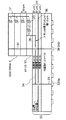
図1は、本発明の第1の実施の形態に係るメモリシステム(半導体集積回路装置)の構成を示す概略図であって、(a)は縦断面構造を示す図、(b)は平面構成を示す図である。 FIG. 1 is a schematic diagram showing a configuration of a memory system (semiconductor integrated circuit device) according to a first embodiment of the present invention, where (a) is a diagram showing a longitudinal sectional structure, and (b) is a plan configuration. FIG.
図1のメモリシステムは、マザーボード5上に搭載されたチップセット4と、複数(ここでは2個のみ示す)のDRAM積層体14a,14bとを有している。各DRAM積層体14は、8〜16個のDRAMチップが積層されたチップ・オン・チップDRAM(COC DRAM)6と、このCOC DRAM6が積層されるインタフェースLSI(I/F LSI)12と、このI/F LSI12の下に配設されたSi部10とPCB部11からなるインタポーザ7とを備えている。
The memory system of FIG. 1 has a chip set 4 mounted on a mother board 5 and a plurality (only two are shown here) of DRAM stacked
各インタポーザ7のSi部10は、Si基板8と絶縁層部9とを含む。インタポーザ7のSi部10とPCB部11とは、フリップチップ接続されている。インタポーザ7のPCB部11とマザーボードとは、半田ボールで接続されている。
The
チップセット4とI/F LSI12aの間の信号伝送は、ポイント・トゥ・ポイント接続により行われる。チップセット4とI/F LSI12aの間の配線は、マザーボード5中では、特性インピーダンスZ0となるように行われる。また、この配線は、インタポーザ7中では、水平方向に関し、絶縁層部9aを通る配線15aとして実現される。
Signal transmission between the chip set 4 and the I /
I/F LSI12aとI/F LSI12b間の信号伝送も、ポイント・トゥ・ポイント接続により行われる。I/F LSI12aとI/F LSI12b間の信号線も、マザーボード5中では、特性インピーダンスZ0で配線される。また、インタポーザ7b中では、水平方向に関し、絶縁層部9を通る配線15bとして実現される。
Signal transmission between the I /
インタポーザ7a,7b中の配線15a,15bに対して電位基準を与えるレファレンスプレーン16a,16bは、それぞれPCB11a,11b内に設けられている。このレファレンスプレーン16a,16bの働きにより、配線15a,15b夫々の特性インピーダンスをZ0に設定し、DC抵抗を3オーム程度以下にする。インタポーザ7中の配線15とレファレンスプレーン16に関する詳細は後述する。
Reference planes 16a and 16b for providing a potential reference to the
以上のようにして図1のメモリシステムでは、ポイント・トゥ・ポイント接続部の特性インピーダンスが全線に渡りZ0に設定される。また、これらのポイント・トゥ・ポイント接続の受信側は、終端抵抗Z0で終端され、ドライバ側は、ソース抵抗Z0でインピーダンス整合させてある。その結果、ポイント・トゥ・ポイント接続部の信号伝送は、反射が抑えられ、良好な信号インテグリティ(Signal Integrity)が得られる。 As described above, in the memory system of FIG. 1, the characteristic impedance of the point-to-point connection is set to Z0 over the entire line. The receiving side of these point-to-point connections is terminated with a terminating resistor Z0, and the driver side is impedance matched with a source resistor Z0. As a result, the signal transmission at the point-to-point connection is suppressed in reflection, and good signal integrity is obtained.
このポイント・トゥ・ポイント接続部の信号は、DQ信号、CA信号等の情報を含むいわゆるプロトコル信号であり、その信号本数は150−200本である。また、このポイント・トゥ・ポイント接続部の信号は、DRAMのデータレートの4〜6倍速で伝送される。例えば、DRAMのデータレートを1.6Gbpsとすると、このポイント・トゥ・ポイント接続部でのデータレートは6.4〜9.6Gbpsである。なお、積層されるDRAMは、1チャンネルあたり8バイトとすると、×64ビット構成が望ましい。 The signal at this point-to-point connection is a so-called protocol signal including information such as a DQ signal and a CA signal, and the number of signals is 150-200. The signal at the point-to-point connection is transmitted at 4 to 6 times the DRAM data rate. For example, if the data rate of the DRAM is 1.6 Gbps, the data rate at this point-to-point connection is 6.4 to 9.6 Gbps. Note that the DRAM to be stacked preferably has a x64-bit configuration, assuming 8 bytes per channel.
各DRAM積層体14において、I/F LSI12とCOC DRAM6間の信号伝送は、COC DRAM6を積層方向(垂直方向)に貫いて形成される貫通電極17を介してなされる。図1には貫通電極17を1本のみ示しているが、実際には、DQ、CA、電源等の信号用に必要な本数分設けられる。信号としては、DQ信号、DQS信号、CA信号、CLK等があり、これらは種類毎に区別されて授受されるが、貫通電極17を含む配線は全て同じトポロジー(Topology)である。このため、各信号のスキューはほとんど発生しない。また、貫通電極17の長さも、8チップ積層の場合で0.4mm程度と短く、この部分は集中定数とみなせるので、終端抵抗は不要である。従って、I/F LSI12とCOC DRAM6との間の信号伝送を行った場合に、終端抵抗による電力消費がないので、低消費電力動作が可能となる。
In each DRAM stacked body 14, signal transmission between the I /
先にも述べたが、チップセット4とI/F LSI12a間、及び隣り合うI/F LSI12a,12b間は、ポイント・トゥ・ポイント接続で信号の授受を行う。データレートは6.4〜9.6Gbps程度である。信号種は、メモリに必要な、DQ(データ),CA(コマンドアドレス)信号等の情報を含んだ差動伝送プロトコル信号等で、その信号本数は150〜200本程度である。これに対応して、PCB部11のボール数は、電源、GND用を含め、300〜400個程度となる。そして、総ボール位置数は、ウインドウ(Window)、及び無接続(No connection)等を含めると500〜600個となる。ここで、ボールピッチを0.8mmと仮定すると、PCB部11の大きさは、20mm×20mm程度となる。
As described above, signals are exchanged between the chip set 4 and the I /
一方、I/F LSI 12とCOC DRAM 6の間の信号は、DQ,CA,CLK(クロック)等であり、種類毎に信号の授受が行われる。DQ系信号のデータレートは1.6Gbps程度である。ここで使用される信号本数は、差動伝送信号、シングルエンド(Single-ended)伝送信号を含め、200〜250本程度である。
On the other hand, signals between the I /
COC DRAM6の大きさは、大体10mm×10mm程度であり、I/F LSI12の大きさはそれに合わせてある。I/F LSI12をフェースアップ(Face up)配置とした場合、I/F LSI12には、電源、GND等を含め、400本程度の貫通電極を設ける必要がある。
The size of the
I/F LSI12において、貫通電極を設けることができる場所は限られているので、貫通電極のピッチを40μm程度とせざるを得ない場合も存在する。そのため、I/F LSI12と、0.8mm程度のビア(Via)ピッチを有するPCB部11とを直接接続するのは困難である。そこで、I/F LSI12とPCB部11との間に、信号(配線)のピッチ変換用のインタポーザとして、I/F LSI12と同じ物質のSi部10を介在させている。
In the I /
Siインタポーザ10の下面の電極端子には、フリップチップ接続で、ほぼ同一サイズのPCB基板11が接続される。そしてPCB基板11は、その下面に形成された半田ボールを用いてマザーボードに接続される。この構成により、システムの信頼性が向上する。また、COC DRAM6、I/F LSI12、Siインタポーザ10、PCB11からなるDRAM積層体14を単一のパッケージとみなせるので、その取扱いが容易である。更に、PCB部11に信号配線に電位基準を与えるレファレンスプレーン16を設けているので、Siインタポーザ10に設けられる配線15の特性インピーダンスとDC抵抗とをそれぞれ適切な値に設定することができる。このように、PCB11は、電気特性、信頼性、及び取り扱いの容易化を実現する。
A
インタポーザ7中の配線15の長さは、10〜15mm程度になる場合があるので、インタポーザ7の配線に、上記のようにして良好な伝送線特性を持たせておくことは重要である。
Since the length of the wiring 15 in the
次に、図1のメモリシステムの動作について説明する。 Next, the operation of the memory system of FIG. 1 will be described.
まず、チップセット4から、COC DRAM6aにデータを書き込む場合について述べる。チップセット4は、DQ信号、CA信号等の情報を含むプロトコル信号をI/F LSI12aへ出力する。I/F LSI12aは、プロトコルに従ってチップセット4からの信号を解読し、COC DRAM6aへ、CA信号、DQ信号、CLK等を出力する。そして、COC DRAM6aは、I/F LSI12aから出力される信号に従い、所定のアドレスにデータを書き込む。
First, a case where data is written from the chip set 4 to the
COC DRAM6bにデータを書き込む場合は、I/F LSI12aがプロトコル信号をI/F LSI12bへ送信し、I/F LSI12bが、プロトコルに従って信号を解読し、COC DRAM6bへ、CA信号、DQ信号、CLK等を出力する。その結果、COC DRAM6bは、COC DRAM6aと同様に、I/F LSI12bから出力される信号に従い、所定のアドレスにデータを書き込む。
When writing data to the
次に、COC DRAM6aからデータを読み出す場合について述べる。
Next, a case where data is read from the
チップセット4は、CA信号等の情報を含むプロトコル信号をI/F LSI 12aに供給する。I/F LSI12aは、プロトコルに従ってチップセット4からの信号を解読し、COC DRAM6aへ、CA信号、CLK等を出力する。COC DRAM6aは、I/F LSI12aからのCA信号等に応答して、所定のアドレスからデータを読み出す。I/F LSI12aは、読み出されたデータを取り込み、プロトコル信号としてチップセット4へ送出する。
The chip set 4 supplies a protocol signal including information such as a CA signal to the I /
COC DRAM6bからデータを読み出す場合は、チップセット4が、CA信号等の情報を含むプロトコル信号をI/F LSI12aを介してI/F LSI12bに供給する。I/F LSI12bは、プロトコルに従ってチップセット4からの信号を解読し、COC DRAM6bへ、CA信号、CLK等を出力する。COC DRAM6bは、I/F LSI12bからのCA信号等に応答して、所定のアドレスからデータを読み出す。読み出されたデータを、I/F LSI12bは取り込み、I/F LSI12aを介して、プロトコル信号としてチップセット4へ出力する。
When reading data from the
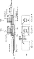
次に、図2を参照して、図1のシステムメモリに使用されるインタポーザ7の原理について説明する。
Next, the principle of the
図2は、図1のDRAM積層体14の左半分の断面図を示している。 FIG. 2 shows a cross-sectional view of the left half of the DRAM stack 14 of FIG.
上述のように、インタポーザ7のSi部10は、Si基板部8と絶縁層部9とを含む。絶縁層部9は、厚み1μm程度の複数の絶縁層と、各絶縁層間の配線層とからなる。配線15は、絶縁層部9の配線層をパターニングするなどして形成される。また、配線15は、ブラインドビアにより、Si部10の下面に形成された接続端子に電気的に接続される。配線15は、例えば、幅100μm、厚み0.5μmである。Si部10は、さらに、Si基板部8及び絶縁層部9を貫通し、配線15に接続される貫通電極22を有している。Si部10の絶縁層及び配線15は、通常のLSI製造工程によって製造できるサイズなので工業生産に適している。
As described above, the
PCB11のレファレンスプレーン16(即ち、GND層プレーン)は、PCB11の上面から100μm程度離れた位置に形成されている。レファレンスプレー16は、Si部10の配線15とともに伝送線構造を形成する。レファレンスプレーン16と配線15との距離を100μm以上としたことにより、この伝送線構造の特性インピーダンスは約50オームとなる。また、配線15のDC抵抗Rdcは、その長さを10mmとして、Rdc=(1/58e6)×(10e−3)/((0.5e−6)×(100e−6))=3.4オーム、となる。抵抗Rdcは、配線15の厚みと幅を調整することによって、より低い値にすることが可能である。
The reference plane 16 (ie, GND layer plane) of the
PCB11の下面には、約800μmのピッチで複数の半田ボールが形成されている。半田ボールは、上述したようにマザーボート5に接続固定される。
A plurality of solder balls are formed on the lower surface of the
信号用の半田ボール20に入った信号は、PCB11のビア21を通って、Si部10に入る。その後、絶縁層部9を通る配線15によって、I/F LSI12の下の所定位置までいき、Si部10とI/F LSI12とを貫通する貫通電極22介してI/F LSI12に入力される。I/F LSI12に入った信号は、I/F LSI12内で論理回路23等を経て、COC DRAM6の貫通電極17を介して各DRAMに到達する。各DRAMからの信号は、上記経路とは逆の経路を辿り、半田ボール20を介してマザーボードへと到達する。
A signal entering the
GND電位は、半田ボール24に供給され、PCB11のビア25を介して、Si部10に入り、Si部10、I/F LSI12、COC DRAM6を貫通する貫通電極26によって各DRAMに供給される。また、PCB11内のレファレンスプレーン(GND層プレーン)16にも供給される。
The GND potential is supplied to the
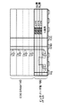
図3を参照して、インタポーザ7がPCB11を備える必要性について説明する。
The necessity for the
図3は、Si部30のみからなるインタポーザを含むDRAM積層体の左半分断面図である。
FIG. 3 is a left half sectional view of a DRAM stacked body including an interposer composed of only the
Si部30は、Si基板8と絶縁層部31とを有している。絶縁層部31は、厚み1μmの複数の絶縁層を含み、これら絶縁層の間に配線34及びGND層プレーン38が形成されている。配線34とGNDレファレンスプレーン38とは、互いに異なる絶縁層間に配置される。
The
また、Si部30は、Si基板8及び絶縁層部31を貫通し、配線34に接続される貫通電極33と、Si基板8及び絶縁層部31を貫通し、さらにCOC DRAM6を貫通するとともにGNDレファレンスプレーン38に接続される貫通電極37と、その下面に形成された複数のフリップチップ電極とを有している。
The
信号用のフリップチップ電極32からSi部30に入った信号は、Si部30の貫通電極33、絶縁層部31を走る配線34を介してI/F LSI12の貫通電極35に入力される。I/F LSI12に入った信号は、I/F LSI12内の論理回路23等を経て、COC DRAM6の貫通電極17に到達し、各DRAMに入力される。各DRAMからチップセットへ向かう信号は、上記経路と逆の経路を辿り、フリップチップ電極32へ到達する。
A signal that enters the
GND電位は、フリップチップ電極36に供給され、Si部30に入り、Si部30、I/F LSI12、COC DRAM6を貫通する貫通電極37に供給され、各DRAM及びGNDレファレンスプレーン38に供給される。
The GND potential is supplied to the
図3のインタポーザにおいて、配線34は、GNDレファレンスプレーン38とともに伝送線構造を形成する。この構成で特性インピーダンスを約50オームにするには、配線34を、幅1μm、厚さ0.5μm程度としなければならない。しかし、この場合、配線34のDC抵抗Rdcは、その長さを10mmとして、Rdc=(1/58e6)×(10e−3)/((0.5e−6)×(1e−6))=340オーム、となる。この値は、伝送線としては大き過ぎる値である。つまり、Si部だけでは、工業生産に向いたサイズで、DC抵抗と特性インピーダンスの両方を満たす伝送線構造のインタポーザを作ることは難しい。
In the interposer of FIG. 3, the
なお、図3に示すSi部30のように、絶縁層部がCOC DRAM側に位置し、Si基板がマザーボード側に位置する場合であって、その下にレファレンスプレートを有するPCBを設けることにより、図2のインタポーザ7と同様に、良好な特性を有する伝送線構造を形成することができる。ただし、その場合は、配線とレファレンスプレーンとの間に大きな比誘電率εr(=12)を持つSi基板部8が位置するので、図2と同じサイズの場合、特性インピーダンスは小さくなる。
In addition, as in the
次に、図4を参照して、インタポーザ7についてより詳細に説明する。
Next, the
図4は、インタポーザ7の詳細構造図であって、図2同様、DRAM積層体14の左半分の断面図を示している。図2と異なる点は、Si部10の絶縁層部9が5層の絶縁層からなり、各絶縁層間にVDD線、GND線、第1及び第2の信号配線が形成されている点、及びこれらに接続される貫通電極あるいはビアを有している点である。
FIG. 4 is a detailed structural diagram of the
図4のインタポーザ7において、半田ボール40に入った信号は、PCB11のビア41を通って、Si部10に入る。Si部10に入った信号は、絶縁層部9を通る配線42によって、I/F LSI12の下の所定位置までいき、Si部10とI/F LSI12を貫通する貫通電極43に到達する。貫通電極43を介してI/F LSI12に入った信号は、I/F LSI12内で論理回路23等を経て、COC DRAM6の貫通電極17を介して各DRAMに到達する。各DRAMからの信号は、上記と逆の経路を辿り、半田ボール40に到達する。
In the
他の半田ボール44に入った信号も同様にして、COC DRAM6に到達する。ただし、この信号は半田ボール40に入った信号が通る配線42とは、異なる配線層に形成された配線45を通る。配線42と配線45とを異なる配線層に形成することにより、各配線層の配線数を減らすことができ、レイアウトが容易になる。
Similarly, signals entering the
I/F LSI12の下に位置する半田ボールに入る信号も、図示はしないが、上記と同様の経路を辿る。但し、Si部10とI/F LSI12とを貫通する貫通電極の位置によっては、絶縁層部9に設けられる配線は不要である。
A signal that enters the solder ball located under the I /
半田ボール46に供給されたGND電位は、PCB11のビア47を介して、Si部10に入り、Si部10、I/F LSI12、COC DRAM6を貫通する貫通電極48を介して各DRAMに供給される。また、PCB11内のGNDレファレンスプレーン16及びSi部10のGNDレファレンス線49にも供給される。
The GND potential supplied to the
I/F LSI12領域の下以外に形成された半田ボール50に供給されたGND電位は、PCB11のビア51を介して、GNDレファレンスプレーン16供給され、また、Si部10の貫通電極52を介してGNDレファレンス線49に供給される。ここで、貫通電極52の代わりにブラインドビアを用いることも可能であるが、貫通電極52を用いた場合は、後述する貫通電極53との間にデカップリングコンデンサを接続することが可能である。デカップリングコンデンサは、Si部10の上面に形成できる。
The GND potential supplied to the
半田ボール54に供給されたVDD電位は、PCB11のビア55を介して、Si部10に入り、Si部10、I/F LSI12、COC DRAM6を貫通する貫通電極56によって各DRAMに供給される。また、PCB11内のVDDプレーン57及びSi部10のVDD線58にも供給される。
The VDD potential supplied to the
I/F LSI12領域の下以外に形成された半田ボール59に供給されたVDD電位は、PCB11のビア60を介して、VDDプレーン57に供給され、また、Si部10の貫通電極53を介してVDD線58に供給される。ここで、貫通電極53の代わりにブラインドビアを用いることも可能であるが、貫通電極53を用いることにより、上述した通り、GND電位貫通電極52との間にデカップリングコンデンサを接続することができる。
The VDD potential supplied to the
PCB11内のGNDレファレンスプレーン16は、PCB11の上面から100um程度の所に設けられている。また、絶縁層9内を通る配線42、45は、夫々幅が100um、厚さが0.5um程度である。絶縁層部9の各絶縁層は、厚み1um程度である。これらの配線や絶縁層は通常のLSIの製造工程で製造できるサイズの範囲内であるので、工業生産に向いている。
The
ここで、配線42、45とGND レファレンスプレーン16で伝送線構造を形成している。この構成の特性インピーダンスは約50オームである。一方、配線42、45の各々のDC抵抗Rdcは、その長さを10mmとして、Rdc=(1/58e6)x(10e−3)/((0.5e−6)x(100e−6))=3.4オーム、となる。各配線の厚さと幅を調整することによって、DC抵抗Rdcをより低い値にすることは可能である。
Here, a transmission line structure is formed by the wirings 42 and 45 and the
図4では、PCB11内のGNDレファレンスプレーン16がVDDプレーンよりもSi部10側に位置する例を示したが、VDDプレーン57が、GNDプレーン16よりもSi部10側に位置する用にしてもよい。この場合、VDDプレーン57が、配線52,54に電位基準を与えるレファレンスプレーンとなる。即ち、配線42、45は、VDDレファレンスプレーン57とともに伝送線構造を形成する。
FIG. 4 shows an example in which the
また、図4の例では、Si部10に、VDD線58、GND線49を設けたが、これは電源強化のためであって、必ずしも必要ではない。また、これらVDD線58はGND線49は、絶縁層部9を走る信号配線42、45のレファレンスとならないように布線しなければならない。つまり、VDD線58及びGND線49は、上から見て信号配線52,54と重ならないようにしなければならない。
In the example of FIG. 4, the
本実施の形態によれば、ポイント・トゥ・ポイント接続されたチップセット4とI/F LSI12間を、上述のように全線伝送線構造にすることができる。よって、終端抵抗やソース抵抗を伝送線の特性インピーダンスと整合させることによって、信号インテグリティ(Signal Integrity)良く、高速伝送をすることができる。
According to the present embodiment, the entire line transmission line structure can be formed between the chip set 4 and the I /
また、本実施の形態によれば、I/F LSI12とCOC DRAM6との間は、貫通電極を介して短距離で接続される。具体的には、DRAMチップ厚を1個あたり50μmとして、8枚積み重ねた場合でも、その距離は0.4mmである。このため、COC DRAM6において、各信号のスキューの発生がほとんどなく、高速動作が可能となる。また、I/F LSI12とCOC DRAM6との間の信号伝播時間は、信号の立上がり/立下がり時間に比べて短いため、COC DRAM6を集中定数回路として扱うことが可能となる。それゆえ、COC DRAM6の各DRAMに終端抵抗を設ける必要が無く、終端抵抗で消費される電力が無いので、低消費電力動作が可能となる。
Further, according to the present embodiment, the I /
また、本実施の形態によれば、DRAMのメモリ容量を増やす場合、2次元的に平面にDRAMを並べて増やすのではなく、3次元的に積層すればよいので、占有面積を増加させることなくメモリ容量を増加させることができる。この場合、高さの増加も1チップ当り50μm程度である。 Further, according to the present embodiment, when the memory capacity of the DRAM is increased, it is only necessary to stack the DRAMs three-dimensionally rather than arranging the DRAMs two-dimensionally in a plane, so that the memory is not increased. The capacity can be increased. In this case, the increase in height is about 50 μm per chip.
なお、上記実施の形態では、PCB10にレファレンスプレーンを設けたが、マザーボードにレファレンスプレーンを設けることとも原理的には可能である。この場合、PCB10は不要となるので、Si部10が直接マザーボードにフリップチップ接続される。
In the above embodiment, the reference plane is provided on the
次に、図5及び図6を参照して、インタポーザ7のSi部10、I/F LSI12、及びCOC DRAM6を夫々貫通する貫通電極の位置関係について述べる。
Next, with reference to FIG. 5 and FIG. 6, the positional relationship of the through electrodes penetrating the
図5に示すように、DRAMチップ70の素子形成領域は、その大部分がメモリセルアレイ領域71によって占められる。メモリセルアレイ領域71には、多数のトランジスタが密集して形成されるので、この領域内に貫通電極を形成することはできない。従って、貫通電極を設けることができる場所は、メモリセルアレイ領域71同士の間に位置する周辺回路領域72(センターライン領域)、あるいはメモリセルアレイ領域71の外周に位置するチップ周辺領域73に限られる。このような制限下において、インタポーザ7のSi部10、I/F LSI12、及びCOC DRAM6を夫々貫通する貫通電極は、図6に示すような位置関係にある。
As shown in FIG. 5, most of the element formation region of the DRAM chip 70 is occupied by the memory cell array region 71. Since a large number of transistors are densely formed in the memory cell array region 71, a through electrode cannot be formed in this region. Therefore, the place where the through electrode can be provided is limited to the peripheral circuit region 72 (center line region) located between the memory cell array regions 71 or the chip peripheral region 73 located on the outer periphery of the memory cell array region 71. Under such restrictions, the through electrodes penetrating the
図6は、Si部10、I/F LSI12、及びCOC DRAM6を夫々貫通する貫通電極の位置を示す平面透視図である。なお、貫通電極の数は、実際のインタポーザ7よりも少ない。また、図4と同一のものには、同一の参照符号を付している。
FIG. 6 is a perspective plan view showing the positions of the through electrodes penetrating the
図6において、外側の大きい四角形は、インタポーザ7(Si部10及びPCB11)を表し、内側の小さい四角形は、COC DRAM6及びI/F LSI12を表す。
In FIG. 6, the outer large square represents the interposer 7 (
マトリクス状に配置された二重丸の外側の丸(大きい丸)は、インタポーザ7の下面に形成される半田ボールを表している。これら大きい丸のうち、白丸は信号用、黒丸はGND用、ハッチングのかかったものはVDD用あるいはVref用の半田ボールを表している。
The outer circles (large circles) of the double circles arranged in a matrix form represent solder balls formed on the lower surface of the
二重丸の内側の丸及びその他の一重丸(小さい丸)は、PCB11に形成されたビアや、Si部10、I/F LSI12及びCOC DRAM6の夫々に形成され、あるいはこれらに共通に形成された貫通電極を示す。小さい丸のうち黒丸は、COC DRAM6の貫通電極である。また、二重丸の内側の丸は、基本的に、ボールの真上に形成されたPCB11のビアである。
The inner circle of the double circle and other single circles (small circles) are formed in the vias formed in the
図5を参照して説明したように、COC DRAM6に形成される貫通電極は、DRAMチップの周辺回路領域及びチップ周辺領域に限定される。インタポーザ7のSi部10及びI/F LSI12を貫通する貫通電極は、互いに対応するCOC DRAM6の貫通電極とPCB11のビアとの接続が容易に行えるように設けられる。
As described with reference to FIG. 5, the through electrode formed in the
小さい四角形の外側に配置された信号用の半田ボール上に形成されたPCB11のビアは、インタポーザ7のSi部10に形成された絶縁層部9を通る配線により、Si部10及びI/F LSI12を貫通する貫通電極に接続される。I/F LSI12は、内部回路23を介して、自身を貫通する貫通電極とCOC DRAM6を貫通する貫通電極とを接続する。例えば、半田ボール40の上に形成されたPCB11のビア41は、配線42によってSi部10及びI/F LSI12を貫通する貫通電極43に接続される。また、貫通電極43は、I/F LSI12の内部回路を介してCOC DRAM6の貫通電極17に接続される。COC DRAM6に形成する貫通電極を、メモリセルアレイ領域以外の周辺回路領域及びチップ周辺領域としたことにより、DRAMチップのレイアウトを効率的に行うことができる。
The vias of the
小さい四角形の内側に配置された信号用の半田ボール75上に形成されたPCB11のビアは、その真上にSi部10及びI/F LSI12を貫通する貫通電極76が存在する場合には、絶縁層部9を通る配線を介さずに直接接続される。真上にSi部10が存在しないPCB11のビアは、内側の四角形の外側に配置された半田ボール状に形成されたビアと同様、絶縁層部9を通る配線を介して、Si部10及びI/F LSI12を貫通する貫通電極に接続される。
The vias of the
小さい四角形の内側に位置するGND電位用の半田ボール46の上に形成されたPCB11のビア47は、その真上に形成されたSi部10、I/F LSI12及びCOC DRAM6を貫通する貫通電極48に、絶縁層部9の配線を介することなく接続される。
A via 47 of the
同様に、VDD電位用の半田ボール54上に形成されたPCB11のビア55も、その真上に形成されたSi部10、I/F LSI12及びCOC DRAM6を貫通する貫通電極56に、絶縁層部9の配線を介することなく接続される。Vref電位用の半田ボール77上に形成されたビアについても同様である。
Similarly, the via 55 of the
小さい四角形の外側に配置されたGND電位用の半田ボール50の上に形成されたPCB11のビア51は、その真上に形成されたSi部10を貫通する貫通電極52に直接接続される。
The via 51 of the
同様に、VDD電位用の半田ボール59の上に形成されたPCB11のビア60は、その真上に形成されたSi部10を貫通する貫通電極53に直接接続される。
Similarly, the via 60 of the
以上のように、I/F LSI12の下の領域(小さい四角形の内側)にあるGND用及びVDD用の半田ボールの真上に、PCB11のビアと、Si部10、I/F LSI12及びCOC DRAM6を貫通する貫通電極とを配置するようにしたことで、各DRAMチップに最短距離でGND電位及びVDD電位を供給することができる。また、I/F LSI12の下の領域外(小さい四角の外側)にあるGND用VDD用の半導体ボールの真上に、PCB11のビアとSi10を貫通する貫通電極とを配置し、PCB11内のGNDプレーンやVDDプレーン、及びSi部10のGND線やVDD線を介してCOC DRAM6にGND電位及びVDD電位を供給するようにしたので、各DRAMチップへの安定した電源供給が可能である。
As described above, the vias of the
また、I/F LSI12の下の領域外に、Si部10を貫通するVDD電位貫通電極53とGND電位貫通電極52とを設けることにより、これらの間にデカップリングコンデンサ78を接続することができる。デカップリングコンデンサの存在により、COC DRAM6に対してさらに安定した電源供給が可能である。また、デカップリングコンデンサは、他の同様な箇所にも設置可能である。
Further, by providing the VDD potential through
図7は、本発明の第2の実施の形態に係るメモリシステムの構成を示す概略図である。図7において、図1と同一の物には同一の参照符号を付している。 FIG. 7 is a schematic diagram showing a configuration of a memory system according to the second embodiment of the present invention. 7, the same components as those in FIG. 1 are denoted by the same reference numerals.
本実施の形態に係るメモリシステムは、第1の実施の形態に係るメモリシステムと基本構成は同じである。異なる点は、PCB11とマザーボード5との接続に半田ボールではなく、同軸タイプの小型高周波コネクタ80を用いている点である。このコネクタを用いることによって、更に高速性能を向上させることができる。
The memory system according to the present embodiment has the same basic configuration as the memory system according to the first embodiment. The difference is that a small high-frequency connector 80 of the coaxial type is used for the connection between the
次に、図8を参照して、第1及び第2の実施の形態に係るメモリシステムに共通の、IF/LSI12の配置方法について説明する。
Next, a method for arranging the IF /
図8(a)及び(b)から理解されるように、I/F LSI12に下面側から出入りする信号群85の本数(ここでは1本)と、上面側から出入りする信号群86の本数(ここでは2本)とが異なっている場合、I/F LSI12をフェースアップ配置とするか、フェースダウン配置とするかによって、I/F LSI12に形成しなければならない貫通電極の数が異なる。つまり、I/F LSI12に下面側から出入りする信号群85の本数よりも、上面側から出入りする信号群86の本数のほうが多い場合は、図8(a)に示すように、フェースアップ配置したほうが、貫通電極の本数を少なくできる。なお、ここでいうフェースアップ配置とは、I/F LSI12のトランジスタ形成領域が上面(COC DRAM6側)となる配置である。
As can be understood from FIGS. 8A and 8B, the number of
第1及び第2の実施の形態に係るメモリシステムでは、I/F LSI12に下面側から出入りする信号よりも、上面側から出入りする信号のほうが数が多いので、フェースアップ配置とすることにより、貫通電極の数を減らすことができ、それによって製造歩留まりの向上を図ることができる。
In the memory system according to the first and second embodiments, the number of signals entering / exiting the I /
図9(a)は、第1及び第2の実施の形態に係るメモリシステムに用いられるI/F LSI12の構成例を示す図である。図9(b)は、一般的なI/F LSIの構成例である。
FIG. 9A is a diagram illustrating a configuration example of the I /
図9(b)に示す一般的なI/F LSI90は、下側から入力されるCLKをバッファ92で受け、貫通電極17−1及び17−2を介して、DRAM91−1及びDRAM91−2に供給する。
The general I / F LSI 90 shown in FIG. 9B receives the CLK input from the lower side by the
DRAM91−1では、CLK分配回路93−1がCLKをチップ内に分配し、バッファ94−1が分配されたCLKをフリップフロップ群95−1に供給する。同様に、DRAM91−2でも、CLK分配回路93−2がCLKをチップ内に分配し、バッファ94−2が分配されたCLKをフリップフロップ群95−2に供給する。 In the DRAM 91-1, the CLK distribution circuit 93-1 distributes CLK within the chip, and the buffer 94-1 supplies the CLK distributed to the flip-flop group 95-1. Similarly, also in the DRAM 91-2, the CLK distribution circuit 93-2 distributes CLK within the chip, and the buffer 94-2 distributes CLK to the flip-flop group 95-2.
ここで、バッファ92の遅延時間をta、CLK分配回路93−1の遅延時間をtb1、バッファ94−1の遅延時間をtc1、CLK分配回路93−2の遅延時間をtb2、バッファ94−2の遅延時間をtc2とする。また、貫通電極1チップ分の遅延時間を3psとする。すると、I/F LSI90にCLKが入ってから、フリップフロップ群95−1に到着するまでの時間は、ta+tb1+tc1+3psで表される。また、I/F LSI90にCLKが入ってから、フリップフロップ群95−2に到着するまでの時間は、ta+tb2+tc2+6psで表される。そして、これらの時間差を求めると、(tb2−tb1)+(tc2−tc1)+3psとなる。つまり、この時間差には、DRAMにおけるCLK分配回路93とバッファ94の特性ばらつき分が含まれる。
Here, the delay time of the
一方、図9(a)に示すI/F LSI12では、バッファ92aが下側から入力されるCLKを受け、CLK分配回路93aがCLKをチップ内に分配し、バッファ94aが分配されたCLKを貫通電極17−1aへ出力する。貫通電極17−1aは、バッファ94aからのCLKをDRAM6−1に供給するとともに貫通電極17−2aに供給し、貫通電極17−2aはDRAM6−2に供給する。DRAM6−1,6−2に供給されたCLKは、それぞれのフリップフロップ群95−1,95−2に供給される。
On the other hand, in the I /
このように、図9(a)に示すI/F LSI12は、各DRAMに共通に必要とされるCLK分配回路93やバッファ94を備えており、それによって、各DRAMの構成を簡略化できる。
As described above, the I /
ここで、バッファ92aの遅延時間をta’、CLK分配回路93aの遅延時間をtb’、バッファ94aの遅延時間をtc’とし、貫通電極1チップ分の遅延時間を3psとする。すると、I/F LSI12にCLKが入ってから、フリップフロップ群95−1に到着するまでの時間は、ta’+tb’+tc’+3psであり、フリップフロップ群95−2に到着するまでの時間は、ta’+tb’+tc’+6psで表される。また、その差は3psで一定である。
Here, the delay time of the
このように、図9(a)のI/F LSI12を用いると、各DRAMのフリップフロップ群95−1,95−2に入力されるCLKの時間差は一定となる。つまり、図9(a)に示すI/F LSI12は、DRAM6の特性ばらつきの影響を受けること無く分配できるので、ばらつきの発生が望ましくないCLKのような信号の伝送に有効である。
As described above, when the I /
次に、図10(a)及び(b)を参照して、本発明の第3の実施の形態に係るメモリシステムについて説明する。図10において、図1と同一のものには同一の参照符号を付してある。 Next, with reference to FIGS. 10A and 10B, a memory system according to a third embodiment of the present invention will be described. 10, the same components as those in FIG. 1 are denoted by the same reference numerals.
図10のメモリシステムが図1のものと異なる点は、DRAM積層体100が、I/F LSI12を有していない点、及び、チップセット102とDRAM積層体との間が一種のポイント・トゥ・ポイント接続(1対多接続)で接続されている点である。つまり、本実施の形態に係るメモリシステムでは、各DRAM積層体100が、COC DRAM6とインタポーザ7とからなり、チップセット102の各ボールに全DRAM積層体100の対応するボールが接続されている。また、チップセット102とCOC DRAM6とは、I/F LSI12を介することなく直接信号の授受を行う。
The memory system of FIG. 10 differs from that of FIG. 1 in that the DRAM stack 100 does not have the I /
チップセット102とDRAM積層体100とを結ぶ信号線は、全線、特性インピーダンスをZ0に設定している。また、これらの信号線には、終端抵抗が接続されている。終端抵抗については、このメモリシステムの動作とともに後述する。 The signal lines connecting the chip set 102 and the DRAM stacked body 100 are all lines, and the characteristic impedance is set to Z0. Also, termination resistors are connected to these signal lines. The termination resistor will be described later together with the operation of this memory system.
チップセット102とDRAM積層体100との間で授受される信号には、双方向信号であるDQ,DQSや、単方向信号であるCA,CLK等がある。これら信号は、チップセットとDRAMとの間で直接授受される信号なので、いわゆるプロトコル信号ではない。信号のデータレートは、DRAMのデータレートを1.6Gbpsとすると、1.6Gbpsである。積層するDRAMは、システムとして、1チャンネルあたり8バイトとすると、×64ビット構成が望ましい。図10は、1チャンネル構成の場合を示している。 Signals exchanged between the chip set 102 and the DRAM stacked body 100 include DQ and DQS that are bidirectional signals, CA and CLK that are unidirectional signals, and the like. These signals are not so-called protocol signals because they are directly exchanged between the chipset and the DRAM. The data rate of the signal is 1.6 Gbps when the DRAM data rate is 1.6 Gbps. The DRAM to be stacked preferably has a x64-bit configuration when the system has 8 bytes per channel. FIG. 10 shows the case of a one-channel configuration.
次に、本実施の形態のメモリシステムの動作と終端抵抗の付け方(終端の方法)について説明する。 Next, the operation of the memory system according to the present embodiment and how to attach a termination resistor (termination method) will be described.
まず、チップセット102から、COC DRAM6aに書き込む場合について述べる。
First, a case where data is written from the chip set 102 to the
チップセット102から、64bitのDQ信号、25bit程度のCA信号等が出力されるとする。このとき、チップセット102の一つのボールが、2つのCOC DRAM6a及び6bにつながっているので、同一の信号が、COC DRAM6aだけでなく、COC DRAM6bにも入力される。そこで、チップセット102は、別の互いに独立するボールからCOC DRAM6a,6bに対して、制御信号を出力する。その結果、COC DRAM6aは、チップセットからのDQ信号等を取り込み、COC DRAM6bは取り込まない。
Assume that a 64-bit DQ signal, a 25-bit CA signal, and the like are output from the chip set 102. At this time, since one ball of the chip set 102 is connected to the two
各信号線の終端は、DRAM積層体100aと100bの両方に遠端終端を設けることにより行われる。遠端終端を設ける場所としては、COC DRAM6が考えられる。各DRAMに持たせても良いし、一番上のDRAMに設置しても良い。DRAM内に終端を設けると、終端抵抗のオン/オフ動作が容易に制御できる。
Termination of each signal line is performed by providing far end terminations in both DRAM stacked
遠端終端を設置する別の場所として、インタポーザ7のSi部10が考えられる。この場合、Si部10に若干のMOSトランジスタの作成が必要となる。信号線の遠端終端から先は、COC DRAM6のみが接続されており、その配線の長さは0.4mm程度なので、信号インテグリティの劣化は実質上無い。また、DRAMに終端抵抗を持たせる必要が無いので、DRAMの負担が小さく、熱発散も容易となる。
As another place where the far end termination is installed, the
さらに遠端終端の別の設置場所として、インタポーザ7のPCB部11が考えられる。信号線の遠端終端から先は、インタポーザ7のSi部10とCOC DRAM6のみが接続されており、その配線長さは0.5mm程度なので、上記と同様信号インテグリティの劣化は実質上無い。また、DRAMに終端抵抗を持たせる必要が無いので、DRAMの負担が小さく、熱発散も容易となる。なお、この場合は、終端抵抗をオフできるようにすることは難しいが、読み出し時に、COC DRAM6の出力ドライバとしてオープンドレイン型のドライバを用いれば特に問題はない。
Furthermore, the
チップセット102から、COC DRAM6bに書き込む場合も上記同様に行われる。
When writing from the chip set 102 to the
次に、COC DRAM6aからデータを読み出す場合について述べる。
Next, a case where data is read from the
チップセット102から、CA信号等がCOC DRAM6aに供給される。このCA信号等は、書き込みの場合と同様にCOC DRAM6bにも供給されるが、制御信号により取り込みが阻止される。COC DRAM6aは、チップセット102から供給された信号を解読し、対応するアドレスからデータを読み出す。COC DRAM6aから読み出されたデータは、チップセット102へ送られ、取り込まれる。また、チップセット102へ送られたデータは、チップセット102のボールを介してCOC DRAM6b側へ伝送される。そのため、COC DRAM6b側での終端が必須である。また、望ましくは、COC DRAM6aのドライバのオン抵抗をZ0に合わせておくとよい。また、COC DRAM6aのドライバがプッシュプル型の場合は、図10に示したCOC DRAM6a側の終端は不要である。
A CA signal or the like is supplied from the chip set 102 to the
COC DRAM6bからデータを読み出す場合も、上記と同様にして行われる。
Data is read from the
本実施の形態に係るメモリシステムによれば、図1のメモリシステムと同様の効果が得られる。さらに、本実施の形態のメモリシステムは、I/F LSIを持たないので、図1のメモリシステムに比べ低消費電力化と低コスト化が可能となる。また、チップセット102のボール数を削減できる。 According to the memory system according to the present embodiment, the same effect as that of the memory system of FIG. 1 can be obtained. Furthermore, since the memory system of this embodiment does not have an I / F LSI, it is possible to reduce power consumption and cost as compared with the memory system of FIG. Further, the number of balls in the chip set 102 can be reduced.
次に、図11を参照して、本発明の第4の実施の形態に係るメモリシステムに説明する。 Next, a memory system according to a fourth embodiment of the present invention will be described with reference to FIG.
図11のメモリシステムは、図10のメモリシステムと基本的に同じであるが、チップセット103と各COC DRAM6とが1対1で信号の授受を行う点で異なっている。つまり、チップセット103が、COC DRAM6a用の端子とCOC DRAM6b用の端子とを別々に備えている。
The memory system in FIG. 11 is basically the same as the memory system in FIG. 10 except that the chip set 103 and each
チップセット103の一つのボールから、COC DRAM6aとインタポーザ7aからなるDRAM群100aのみに信号線が接続され、別のボールから、COC DRAM6bとインタポーザ7bからなるDRAM群100bのみに信号線が接続されている。信号としては、双方向信号であるDQ,DQSや、単方向信号であるCA,CLK等がある。これらは、チップセットとDRAMとの間で直接授受される信号であるので、いわゆるプロトコル信号ではない。
A signal line is connected from only one ball of the chip set 103 to only the
チップセット103とDRAM群100a,100bの間は、ポイント・トゥ・ポイント接続であり、全線の特性インピーダンスをZ0に設定している。信号のデータレートは、DRAMのデータレートを1.6Gbpsとすると、1.6Gbpsである。積層するDRAMは、1チャンネルあたり8バイトとすると、×64bit構成が望ましい。図11のメモリシステムは、2チャンネル構成である。
Point-to-point connection is made between the chip set 103 and the
次に図11のメモリシステムの動作と終端抵抗の付け方について説明する。 Next, the operation of the memory system of FIG. 11 and how to attach a termination resistor will be described.
まず、チップセット103から、COC DRAM6aに書き込む場合について述べる。チップセット103から、64bitのDQ信号、25bit程度のCA信号等が出力される。
First, a case where data is written from the chip set 103 to the
終端法は、DRAM群100aに遠端終端を設ける。遠端終端を設ける場所としては、図10の説明で述べたように3通りが考えられる。また、望ましくは、チップセット103のドライバのON抵抗を伝送線の特性インピーダンスに合わせておくのが良い。
In the termination method, a far-end termination is provided in the
チップセット103から、COC DRAM6bに書き込む場合も同様である。
The same applies when writing to the
この場合、COC DRAM6a及び6bは互いに独立に動作できる。即ち、2チャンネル動作が可能である。
In this case, the
次に、COC DRAM6aからデータを読み出す場合について述べる。チップセット103から、CA信号等がCOC DRAM6aに供給される。COC DRAM6aでは信号を解読し、対応するアドレスからデータを読み出す。読み出されたデータは、チップセット103へ伝送され、取り込まれる。そのため、チップセット103に終端抵抗を設ける。また、望ましくは、COC DRAM6aのドライバのオン抵抗をZ0に合わせておくとよい。また、COC DRAM6aのドライバがプッシュプル型のドライバの場合は、図11に示したCOC DRAM6a側の終端は不要である。
Next, a case where data is read from the
COC DRAM6bからデータを読み出す場合も、上記と同様にして行われる。
Data is read from the
本実施の形態のメモリシステムによれば、図10のメモリシステムと同様の効果が得られる。さらに、2チャンネル動作が可能なので、システム性能をさらに向上できる。 According to the memory system of the present embodiment, the same effect as that of the memory system of FIG. 10 can be obtained. Furthermore, since 2-channel operation is possible, the system performance can be further improved.
図12(a)及び(b)は、図10及び図11に示すメモリシステムにおけるインタポーザ7の半田ボール120への信号の割り振り例を説明するための図である。図12(a)はDRAM積層体100の縦断面図、図12(b)は平面透視図である。なお、インタポーザの配線層数は、配線の混雑度等を考慮して決定される。
FIGS. 12A and 12B are diagrams for explaining examples of signal allocation to the
図10や図11のシステム構成の場合、DQやCA等の信号種別毎に、チップセットとCOC DRAM6との間で信号の授受が行われるので、それらの信号のスキューが小さいことが望ましい。そのため、インタポーザ7に信号が入ってから、COC DRAM6に信号が到達するまでの時間を信号種別毎に一致させることは高速化に有利である。従って、同一属性の信号を、インタポーザ7の中心を中心とする同心円上にある(又は近い)ボールに割り当てる。例えば、図12(b)の例では、一番半径の大きい円に沿って黒丸印で示すボールにDQを割り当て、その内側の円に沿って白丸印で示すボールに、DQを捕まえるためのDQS信号を割り当てる。また、CA信号と、CA信号を捕まえるためのCLK信号とは、DQS信号用の円の一つ内側の円に沿って黒丸印のボールに割り当てる等である。このようにインタポーザ7のボールに信号を割り当てることにより、チップセット102又は103からの信号がインタポーザ7のボールに入るまでの遅延時間を信号種別毎に揃えることができ、小さなスキューで、チップセット102又は103とCOC DRAM6との間の信号の授受が可能となる。
In the case of the system configurations of FIGS. 10 and 11, since signals are exchanged between the chip set and the
図13は、図12(b)の右上部の拡大図である。図13には、ボールの割り振りと、CA信号及びCLK信号用のボールと、COC DRAM6の貫通電極17の端子130との配線接続例とを示している。図13からの理解されるように、CA信号及びCLK信号用のボールと端子130とは、全て略等しい長さで結線されている。他の信号線の配線も同様に、略等しい長さにすることができる。
FIG. 13 is an enlarged view of the upper right part of FIG. FIG. 13 shows ball allocation, CA signal and CLK signal balls, and wiring connection examples of the terminals 130 of the through
次に、図14(a)及び(b)を参照して、第5の実施の形態に係るメモリシステムについて説明する。第1乃至4に係るメモリシステムは、インタポーザ7の平面サイズがCOC DRAM6のそれより大きいものであったが、本実施の形態に係るメモリシステムは、インタポーザの平面サイズがCOC DRAMのそれと同程度のものである。これは、COC DRAMの構成が、×8ビット程度の場合等、信号数が少ない場合に適している。
Next, a memory system according to the fifth embodiment will be described with reference to FIGS. In the memory systems according to the first to fourth aspects, the planar size of the
図14のメモリシステムは、マザーボード142と、マザーボード142上に搭載されたチップセット143及び複数のDRAM積層体144とを有している。
The memory system of FIG. 14 includes a mother board 142, a
各DRAM積層体144は、4チップのDRAMが積層されたCOC DRAM140と、インタポーザ141とが積層されている。
Each DRAM stacked body 144 includes a
各COC DRAM140が×8ビット構成で、1チャンネルが64ビットの場合、8個のDRAM積層体144を一組として使用する。図14は、2チャンネル構成の例を示しており、8個×2列のDRAM積層体144を有している。DRAM積層体の列は、チップセット143から一方向に遠ざかるように並べられる。
When each
インタポーザ141としては、Siインタポーザ又はPCBインタポーザが利用できる。COC DRAMの貫通電極のピッチを最小40μm程度にする場合は、Siインタポーザを用いる。その場合、Siインタポーザは、マザーボード142にフリップチップ接続されるか、同じ大きさのPCB(図示せず)にフリップチップ接続され、PCBの半田ボールを用いてマザーボードに接続される。SiインタポーザとPCBの組み合わせを用いる場合は、その組み合わせ全体をインタポーザとみなせる。 As the interposer 141, a Si interposer or a PCB interposer can be used. When the pitch of the through electrodes of the COC DRAM is set to a minimum of about 40 μm, a Si interposer is used. In that case, the Si interposer is flip-chip connected to the motherboard 142 or flip-chip connected to a PCB (not shown) of the same size, and is connected to the motherboard using PCB solder balls. When a combination of Si interposer and PCB is used, the entire combination can be regarded as an interposer.
一方、COC DRAMの貫通電極のピッチが0.8mm程度の場合は、PCPインタポーザが利用できる。この場合、COC DRAMとPCBインタポーザ141をフリップチップ接続し、PCBインタポーザ141とマザーボードを半田ボールで接続する。あるいは、COC DRAMをマザーボードにフリップチップ接続してもよい。 On the other hand, when the pitch of the through electrodes of the COC DRAM is about 0.8 mm, a PCP interposer can be used. In this case, the COC DRAM and the PCB interposer 141 are flip-chip connected, and the PCB interposer 141 and the motherboard are connected by solder balls. Alternatively, the COC DRAM may be flip-chip connected to the motherboard.
チップセット143とCOC DRAM140との間のDQ,DQS信号伝送は、図示したようなフライ・バイ方式で接続された信号線を用いて行われる。即ち、チップセット143とDRAM積層体144との間で送受される64ビットのDQ,DQS信号のうち、最初の8ビット分が、DRAM積層体144a1,144b1とやり取りされ、次に8ビット分が、DRAM積層体144a2,144b2とやり取りされ、最終の8ビット分が、DRAM積層体144a8,144b8とやり取りされる。これらの信号線は、マザーボード142の特性インピーダンスがZ0の場合、遠端にZ0より低い値の終端抵抗R1で終端される。終端抵抗R1は、伝送線に負荷が接続されるため、容量が増え、実効特性インピーダンスが下がるので、その実効特性インピーダンスに合わせればよい。
DQ and DQS signal transmission between the chip set 143 and the
チップセット143とCOC DRAM140間のCA信号伝送は、図示したようなフライ・バイ方式で接続され、DQ,DQS信号と直交する信号線を用いて行われる。1コピー分のCA信号が、DRAM積層体144a1,144a2,・・・,144a8とやり取りし、別の1コピー分が、DRAM積層体144b1,144b2,・・・,144b8とやり取りする。CA信号を捕まえるためのCLKも同様の信号線により伝送される。これらの信号線は、マザーボード142の特性インピーダンスがZ0の場合は、遠端にZ0より低い値の終端抵抗R2で終端する。
The CA signal transmission between the chip set 143 and the
ここで、DQ信号及びCA信号のいずれも、マザーボード142を走るメインバスからCOC DRAMへと分岐される。そのスタブ長が長いと、そこでの反射が大きくなり、信号のインテグリティが悪化する、従って、いずれの信号線とも、スタブ長は2mm程度以下が望ましい。 Here, both the DQ signal and the CA signal are branched from the main bus running on the motherboard 142 to the COC DRAM. If the stub length is long, reflection at the stub becomes large and signal integrity deteriorates. Therefore, the stub length is preferably about 2 mm or less for any signal line.
次に、図14のメモリシステムの動作について説明する。 Next, the operation of the memory system of FIG. 14 will be described.
まず、チップセット143から、COC DRAM140aに書き込む場合について述べる。
First, a case where data is written from the
チップセット143から、DQ信号、CA信号出力される。ここで、チップセット143のドライバのON抵抗は、それぞれのメインバスの実効特性インピーダンスR1,R2に合わせておくことが望ましい。 A DQ signal and a CA signal are output from the chip set 143. Here, it is desirable that the ON resistance of the driver of the chip set 143 is matched to the effective characteristic impedances R1 and R2 of the respective main buses.
COC DARM140aは、チップセット143からのコマンド信号を解読し、対応するアドレスにデータを書き込む。
The
COC DRAM140bへの書き込みも、上記と同様に行われる。
Writing to the
次に、COC DRAM140aからデータを読み出す場合について述べる。
Next, a case where data is read from the
チップセット143から、CA信号が出力される。COC DRAM140aは、チップセット143からのコマンド信号を解読し、対応するアドレスからデータを読み出す。読み出されたデータは、チップセット143へ伝送され、取り込まれる。読み出し時には、チップセット143に終端抵抗を持たせることが望ましい。その値は、R1である。
A CA signal is output from the
COC DRAM140bからデータを読み出す場合も上記と同様である。
The same applies to the case where data is read from the
本実施の形態に係るメモリシステムによれば、I/F LSIも不要で、インタポーザに伝送線構造を持たせる必要もなく、信号のデータレートもDRAMのスピードと同じで、N倍化された高速部分がないので、実装設計が安価にできる。 According to the memory system of this embodiment, no I / F LSI is required, the interposer does not need to have a transmission line structure, the signal data rate is the same as the DRAM speed, and the N-times high speed is achieved. Since there is no part, mounting design can be made inexpensively.
図15は、図14のメモリシステムのCOC DRAM140の貫通電極の配置について検討するための図である。図15において、大きい丸は、インタポーザ141のボールの位置を示し、小さい黒丸は、COC DRAM140の貫通電極の位置を示す。COC DRAM140の貫通電極を設置できる位置は、図5を参照して説明したような制限があり、ここでは、チップ周辺部に形成されている。
FIG. 15 is a diagram for examining the arrangement of through electrodes of the
マザーボード142からインタポーザ141のボールに入った信号は、COC DRAM140の貫通電極位置まで、横方向に走らなければならない。そのための配線がスタブとなる。図15に示す例では、配線150や151の長さが3mm以上に長くなっており、高速伝送向きではない。
A signal that enters the ball of the interposer 141 from the mother board 142 must run laterally to the through electrode position of the
そこで、図14のメモリシステムでは、図16に示すように、COC DRAM140の貫通電極を配置する。即ち、チップ周辺部のみならず、チップのセンタライン等の周辺回路領域にも設置するようにする。このように、COC DRAM140の貫通電極を配置することにより、各貫通電極が接続されるインタポーザ141のボールまでの距離、即ちスタブ長を短くしている。また、VDDやGNDに接続される貫通電極は、それらが割り当てられる半田ボール160や161の真上に貫通電極を設ける。あるいは、VDDやGNDに割り当てる半田ボール162や163のできるだけ近くに貫通電極を設けて太い配線で接続する。この場合、貫通電極同士を接続してもよい。
Therefore, in the memory system of FIG. 14, the through electrodes of the
図16の例では、貫通電極のピッチが0.8mm程度と大きいので、インタポーザ141として、PCBを用いることが可能で、コスト低減が可能となる。 In the example of FIG. 16, since the pitch of the through electrodes is as large as about 0.8 mm, a PCB can be used as the interposer 141, and the cost can be reduced.
図17は、図14のメモリシステムに適用可能なCOC DRAM140の貫通電極配置の他の例である。図16の例と異なる点は、COC DRAM140の貫通電極を極力センタラインに設置した点である。現在のDRAMは、パッドの大部分がセンタラインに設置されている場合が多いため、そのレイアウト構成を活用でき、設計期間の短縮が可能となる。もちろん、スタブ長が短くできていることは言うまでもない。
FIG. 17 shows another example of the through electrode arrangement of the
この場合には、貫通電極のピッチが最小40μm程度と小さいので、インタポーザ141として、Siインタポーザを用いることが必要である。 In this case, since the pitch of the through electrodes is as small as about 40 μm, it is necessary to use a Si interposer as the interposer 141.
図18は、図17に示す貫通電極配置を持つCOC DRAM140と、それが積層されたSiインターポーザ141の構造を示す縦断面図である。図18において、電源関係の貫通電極は、インタポーザ141とCOC DRAM140とを貫通している。また、信号用の貫通電極は、インタポーザ141の貫通電極とCOC DRAM140の貫通電極の位置は必ずしも一致していない。
FIG. 18 is a longitudinal sectional view showing the structure of the
PCBインタポーザを用いた場合も、図18と同様な構成となる。 Even when a PCB interposer is used, the configuration is the same as in FIG.
次に、図19(a)及び(b)を参照して、本発明の第6の実施の形態に係るメモリシステムについて説明する。 Next, with reference to FIGS. 19A and 19B, a memory system according to a sixth embodiment of the present invention will be described.
本実施の形態に係るメモリシステムが、図14のメモリシステムと異なっている点は、インタポーザ141に代えてSiインタポーザ兼I/F LSI190を備えている点である。即ち、4チップのDRAMが積層されたCOC DRAM140と、Siインタポーザ兼I/F LSI190とが積層されて、DRAM積層体193が構成されている。
The memory system according to the present embodiment is different from the memory system of FIG. 14 in that an Si interposer / I / F LSI 190 is provided instead of the interposer 141. That is, a
図19には、PCB191が示されているが、これは信頼性確保のために設けられたものであって、特性上は特に必要ではない。 FIG. 19 shows the PCB 191, which is provided for ensuring reliability, and is not particularly necessary in terms of characteristics.
マザーボード142上に、チップセット143と、複数のDRAM積層体が、図14と同様の配列及び接続で並べられている。チップセット143とCOC DRAM140の間のDQ,DQS信号伝送は、最初の8ビット分が、DRAM積層体193a1,193b1と行われ、次の8ビット分が、DRAM積層体193a2,193b2と行われ、最終の8ビット分が、DRAM積層体193a8,193b8と行われる。接続方法は、図示したようなフライ・バイ方式であり、チップセット143とCOC DRAM140との間に、Siインタポーザ兼I/F LSI190が介在する。各信号線は、マザーボード142の特性インピーダンスがZ0の場合は、DQ系メインバスの遠端にZ0より低い値の終端抵抗R3を接続して終端すればよい。この終点抵抗R3の値は、伝送線に負荷(Siインタポーザ兼I/F LSI190)が接続されるため、容量が増え、実効特性インピーダンスが下がるので、その実効特性インピーダンスに合わせればよい。
On the mother board 142, a
チップセット143とCOC DRAM140との間のCA信号伝送は、1コピー分が、DRAM積層体193a1,193a2,・・・,193a8と行われ、別の1コピー分が、DRAM群193b1,193b2,・・・,193b8と行われる。CA信号を捕まえるためのCLKも同様である。接続方法は、図示したようなフライ・バイ方式で、DQ,DQS信号用の信号線と直交している。これらの信号の場合も、チップセット143とCOC DRAM140の間に、Siインタポーザ兼I/F LSI190が介在する。マザーボード142の特性インピーダンスがZ0の場合は、CA系メインバスの遠端にZ0より低い値の終端抵抗R4で終端すればよい。
In the CA signal transmission between the chip set 143 and the
本実施の形態に係るメモリシステムでは、DQ、CA信号用のいずれの配線も、マザーボード142を走るメインバスからSiインタポーザ兼I/F LSI190へ分岐され、図14のように、COC DRAMまで直接配線されないので、そのスタブ長が短い。従って、このメモリシステムは、高速化が可能である。 In the memory system according to the present embodiment, both wirings for DQ and CA signals are branched from the main bus running on the motherboard 142 to the Si interposer / I / F LSI 190, and directly wired to the COC DRAM as shown in FIG. Not so, its stub length is short. Therefore, this memory system can be speeded up.
次に図19のメモリシステムの動作について説明する。 Next, the operation of the memory system of FIG. 19 will be described.
まず、チップセット143から、COC DRAM140aに書き込む場合について述べる。
First, a case where data is written from the
チップセット143から、DQ信号、CA信号等が出力される。ここで、チップセット143のドライバのオン抵抗は、それぞれのメインバスの実効特性インピーダンスに合わせておくことが望ましい。 A DQ signal, a CA signal, and the like are output from the chip set 143. Here, it is desirable that the on-resistance of the driver of the chip set 143 is matched to the effective characteristic impedance of each main bus.
Siインタポーザ兼I/F LSI190aは、チップセット143から入力される信号をバッファリングし、COC DRAM140aへ出力する。COC DRAM140aは、Siインタポーザ兼I/F LSI190aからのコマンド信号を解読し、対応するアドレスにデータを書き込む。ここで、Siインタポーザ兼I/F LSI190aとCOC DRAM140aとの間は、終端は不要である。
The Si interposer / I /
COC DRAM140bへの書き込みも、上記と同様に行われる。
Writing to the
次に、COC DRAM140aからデータを読み出す場合について述べる。
Next, a case where data is read from the
チップセット143から、CA信号等が出力される。チップセット143から出力されたCA信号等は、Siインタポーザ兼I/F LSI190aを経て、COC DRAM140aに供給される。COC DRAM140aは、コマンド信号を解読し、対応するアドレスからデータを読み出す。読み出されたデータは、Siインタポーザ兼I/F LSI190aを経て、チップセット143送られ、取り込まれる。従って、読み出し時には、チップセット143に終端抵抗R3を持たせることが望ましい。読み出し時も、Siインタポーザ兼I/F LSI190aとCOC DRAM140a間は、終端は不要である。
A CA signal or the like is output from the
COC DRAM140bからデータを読み出す場合も同様である。
The same applies when data is read from the
本実施の形態に係るメモリシステムによれば、Siインタポーザ兼I/F LSI190で、一旦信号を切るので、スタブ長が短くなり、高速動作が可能になる。また、COC DRAM140の積層数(DRAMチップ数)が増えても、メインバスの負荷は、Siインタポーザ兼I/F LSI190のみで変わらないので、大容量化と高速化を両立できる。さらに、Siインタポーザ兼I/F LSI190のサイズが大きい場合でも、スタブ長を短くできる。 According to the memory system according to the present embodiment, since the signal is once cut by the Si interposer / I / F LSI 190, the stub length is shortened and high-speed operation is possible. Further, even if the number of stacked COC DRAMs 140 (the number of DRAM chips) increases, the load on the main bus does not change only with the Si interposer / I / F LSI 190, so that both large capacity and high speed can be achieved. Furthermore, even when the size of the Si interposer / I / F LSI 190 is large, the stub length can be shortened.
図20は、図19のメモリシステムのDRAM積層体における、COC DRAMの貫通電極と、Siインタポーザ兼I/F LSIの貫通電極及びボールとの位置関係の一例を示す図である。 FIG. 20 is a diagram showing an example of the positional relationship between the through electrode of the COC DRAM, the through electrode of the Si interposer / I / F LSI, and the ball in the DRAM stack of the memory system of FIG.
図20において、大きい丸はSiインタポーザ兼I/F LSIのボール、小さい白丸は、Siインタポーザ兼I/F LSIの貫通電極、小さい黒丸は、COC DRAMの貫通電極である。 In FIG. 20, a large circle is a ball for Si interposer / I / F LSI, a small white circle is a through electrode for Si interposer / I / F LSI, and a small black circle is a through electrode for COC DRAM.
COC DRAMの貫通電極は、図5を参照して説明したように、チップ周辺や、チップのセンタライン等の周辺回路領域にも設置できるので、それらの領域に設置している。また、VDDやGNDに割り当てるボールの真上に、I/F LSIとCOC DRAMの貫通電極が設けられている。信号に割り当てられるボールの真上にはI/F LSIの貫通電極が設置されている。 As described with reference to FIG. 5, the through electrode of the COC DRAM can be installed in the peripheral area of the chip and in the peripheral circuit area such as the center line of the chip. Further, a through electrode of I / F LSI and COC DRAM is provided directly above a ball assigned to VDD or GND. A through electrode of the I / F LSI is installed directly above the ball assigned to the signal.
以上のように貫通電極を設けることによって、電源、GND電位は、最短の直線で、Siインタポーザ兼I/F LSI190とCOC DRAM140に供給されるので安定な電源供給が可能になる。
By providing the through electrode as described above, the power supply and the GND potential are supplied to the Si interposer / I / F LSI 190 and the
図21は、図19のメモリシステムのDRAM積層体における、COC DRAMの貫通電極と、Siインタポーザ兼I/F LSIの貫通電極及びボールとの位置関係の他の例を示す図である。図20と大きく異なる点は、COC DRAM140の貫通電極を極力センタラインに設置した点である。現在のDRAMは、パッドの大部分がセンタラインに設置されている場合が多いので、現在のDRAMチップのレイアウト構成を活用でき、設計期間の短縮が可能となる。
FIG. 21 is a diagram showing another example of the positional relationship between the through electrode of the COC DRAM, the through electrode of the Si interposer / I / F LSI, and the ball in the DRAM stack of the memory system of FIG. A significant difference from FIG. 20 is that the through electrode of the
図22は、図19、図20又は図21のDRAM積層体の縦断面構造を示す図である。図22において、電源関係の貫通電極は、Siインタポーザ兼I/F LSI190とCOC DRAM140を貫通している。また、信号の貫通電極は、Siインタポーザ兼I/F LSI190とCOC DRAM140とで独立して設けられ、Siインタポーザ兼I/F LSI190の中で論理回路等を介して互いに接続されている。なお、Siインタポーザ兼I/F LSI190の中での接続は、DQ等については双方向信号であるので双方向に行われている。
FIG. 22 is a view showing a vertical cross-sectional structure of the DRAM stacked body of FIG. 19, FIG. 20, or FIG. In FIG. 22, the power-related through electrode passes through the Si interposer / I / F LSI 190 and the
以上の説明で判るように、マザーボード142から分岐して、Siインタポーザ兼I/F LSI190に入るスタブ長は短い。 As can be seen from the above description, the stub length branched from the motherboard 142 and entering the Si interposer / I / F LSI 190 is short.
次に、図23(a)及び(b)を参照して本発明の第7の実施の形態に係るメモリシステムについて説明する。 Next, a memory system according to a seventh embodiment of the present invention will be described with reference to FIGS. 23 (a) and (b).
図23のメモリシステムは、メインバスのスピードをN倍速、例えば4倍速にしたメモリシステムである。このメモリシステムは、4〜8個のDRAMチップが積層されたCOC DRAM231と、それと同様の平面サイズを持つインタポーザ(Siインタポーザ兼I/F LSI232及びPCB235)とが積層されたDRAM積層体234を複数備える。また、このメモリシステムは、これらDRAM積層体234を搭載するマザーボード233と、マザーボード上に搭載されたチップセット230とを備える。
The memory system of FIG. 23 is a memory system in which the speed of the main bus is set to N times speed, for example, 4 times speed. This memory system includes a plurality of DRAM stacked bodies 234 in which
COC DRAMは×32ビット構成であり、1チャンネルが64ビットの場合は、図(b)に示すようにDRAM積層体234(234a1,234a2)を2個一組として並置する。複数組のDRAM積層体234は、チップセット230から遠ざかるように一方向に沿って並べられる。図23(b)は、4組のDRAM積層体234の例を示している。 The COC DRAM has a × 32 bit configuration, and when one channel is 64 bits, two DRAM stacks 234 (234a1, 234a2) are juxtaposed as shown in FIG. The plurality of sets of DRAM stacked bodies 234 are arranged along one direction so as to be away from the chip set 230. FIG. 23B shows an example of four DRAM stacks 234.
Siインタポーザ兼I/F LSI232は、図23(a)に示すように、同じ平面サイズのPCB235とフリップチップ接続され、PCB235の半田ボールを用いてマザーボード233に接続される。この場合、Siインタポーザ232とPCB235との組み合わせをインタポーザと見なせる。あるいは、Siインタポーザ兼I/F LSI232は、マザーボード233に直接フリップチップ接続で搭載されてもよい。
As shown in FIG. 23A, the Si interposer / I / F LSI 232 is flip-chip connected to the
チップセット230とCOC DRAM231との間のDQ,DQS信号伝送は、フライ・バイ方式で接続された信号線を用いて行われる。即ち、チップセット230は、DQ,DQS信号のうち8ビット分を4倍速で、DRAM積層体234a1−234d1とやり取りし、残りの8ビット分を同じく4倍速で、DRAM積層体234a2−234d2とやり取りする。
DQ and DQS signal transmission between the chip set 230 and the
DQ,DQS信号用の信号線は、マザーボード233の配線の特性インピーダンスがZ0の場合、メインバスの遠端にZ0より低い値の終端抵抗R5を接続することにより終端される。この終端抵抗R5の値は、伝送線に負荷が接続されるため、容量が増え、実効特性インピーダンスが下がるので、その実効特性インピーダンスに合わせればよい。
When the characteristic impedance of the wiring of the
チップセット230とCOC DRAM231との間のCA信号伝送は、DQ,DQS信号用の信号線と同じくフライ・バイ方式の信号線により行われる。また、この信号線は、DQ,DQS信号用の信号線と平行に設けられる。チップセット230は、CA信号の1コピー分を、DRAM群234a1−234d1とやり取りし、別の1コピー分を、DRAM群234a2−234d2とやり取りする。CA信号を捕まえるためのCLKも同様である。
The CA signal transmission between the chip set 230 and the
CA信号用の信号線は、マザーボード233の特性インピーダンスがZ0の場合、遠端にZ0より低い値の終端抵抗R6を接続することにより終端される。
When the characteristic impedance of the
DQ信号用及びCA信号用のいずれの信号線も、マザーボード233を走るメインバスから各COC DRAM231に向かい分岐される。その分岐によるスタブ長が長いとそこでの信号反射が大きくなり、信号インテグリティが悪くなる。本実施の形態に係るメモリシステムでは、Siインタポーザ兼I/F LSI232がCOC DRAM231とメインバスとの間に挿入されているので、スタブ長が短く、高い信号インテグリティを実現できる。
Both signal lines for the DQ signal and the CA signal are branched from the main bus running on the
次に図23のメモリシステムの動作について説明する。 Next, the operation of the memory system of FIG. 23 will be described.
まず、チップセット230から、COC DRAM231aに書き込む場合について述べる。 First, a case where data is written from the chip set 230 to the COC DRAM 231a will be described.
チップセット230から、DQ信号、CA信号等が出力される。ここで、チップセット230のドライバのオン抵抗は、それぞれのメインバスの実効特性インピーダンスに合わせておくことが望ましい。
From the chip set 230, a DQ signal, a CA signal, and the like are output. Here, it is desirable that the on-resistance of the driver of the
Siインタポーザ兼I/F LSI232aは、チップセット230からの入力信号をバッファリング、あるいは、スピード変換等を実施して、COC DRAM231aへ出力する。ここで、Siインタポーザ兼I/F LSI232aとCOC DRAM231a間は、終端は不要である。 The Si interposer / I / F LSI 232a performs buffering or speed conversion on the input signal from the chip set 230, and outputs it to the COC DRAM 231a. Here, no termination is required between the Si interposer / I / F LSI 232a and the COC DRAM 231a.
COC DRAM231aは、入力されたコマンド信号を解読し、対応するアドレスにデータを書き込む。 The COC DRAM 231a decodes the input command signal and writes data to the corresponding address.
他のCOC DRAM231b等に書き込む場合も、上記と同様である。 The same applies to writing to other COC DRAM 231b and the like.
次に、COC DRAM231aからデータを読み出す場合について述べる。 Next, a case where data is read from the COC DRAM 231a will be described.
チップセット230から、CA信号等が出力される。Siインタポーザ兼I/F LSI232aは、チップセット230からのCA信号等をCOC DRAM231aへ出力する。COC DRAM231aは、入力されたコマンド信号を解読し、対応するアドレスからデータを読み出す。読み出されたデータは、Siインタポーザ兼I/F LSI232aを経て、チップセット230へ送られ、取り込まれる。従って、読み出し時には、チップセット230に終端抵抗を持たせることが望ましい。その値は、メインバスの実効特性インピーダンスに等しい値(R5又はR6)である。読み出し時も、Siインタポーザ兼I/F LSI232aとCOC DRAM231aとの間は、終端は不要である。 A CA signal or the like is output from the chip set 230. The Si interposer / I / F LSI 232a outputs the CA signal or the like from the chip set 230 to the COC DRAM 231a. The COC DRAM 231a decodes the input command signal and reads data from the corresponding address. The read data is sent to the chip set 230 through the Si interposer / I / F LSI 232a and is taken in. Therefore, at the time of reading, it is desirable that the chip set 230 has a termination resistor. The value is equal to the effective characteristic impedance of the main bus (R5 or R6). Even during reading, no termination is required between the Si interposer / I / F LSI 232a and the COC DRAM 231a.
他のCOC DRAM231b等からデータを読み出す場合も、上記と同様である。 The same applies to the case of reading data from other COC DRAM 231b or the like.
本実施の形態に係るメモリシステムによれば、Siインタポーザ兼I/F LSI232で、一度信号を切るので、スタブ長が短くなり、高速動作が可能である。また、COC DRAMのDRAMチップ数を増加させても、メインバスの負荷は、Siインタポーザ兼I/F LSI232のみで変わらないので、大容量化と高速化の両立を図ることができる。さらに、DRAMのビット構成が大きくなって、Siインタポーザ兼I/F LSI232のサイズが大きくなった場合でも、スタブ長を短くできる。 According to the memory system according to the present embodiment, since the signal is once cut by the Si interposer / I / F LSI 232, the stub length is shortened and high-speed operation is possible. Further, even if the number of DRAM chips of the COC DRAM is increased, the load on the main bus does not change only with the Si interposer / I / F LSI 232, so that both large capacity and high speed can be achieved. Further, even when the bit configuration of the DRAM is increased and the size of the Si interposer / I / F LSI 232 is increased, the stub length can be shortened.
図24(a)、(b)に、本発明の第8の実施の形態に係るメモリシステムを示す。このメモリシステムは、×16ビット構成のCOC DRAM241を複数備えている点で図23のメモリシステムと異なっている。 FIGS. 24A and 24B show a memory system according to the eighth embodiment of the present invention. This memory system is different from the memory system of FIG. 23 in that a plurality of COC DRAMs 241 having a × 16 bit configuration are provided.
詳述すると、このメモリシステムは、マザーボード233と、マザーボード上に搭載されたチップセット240と、複数のDRAM積層体244とからなる。
More specifically, this memory system includes a
各DRAM積層体244は、積層された8〜16個のDRAMチップと、Siインタポーザ兼I/F LSI242と、PCB245とを含む。Siインタポーザ兼I/F LSI242はPCB245にフリップチップ接続され、PCB245はマザーボードに半田ボールで接続される。PCB245は、必ずしも必要ではなく、Siインタポーザ兼I/F LSI242を直接マザーボードにフリップチップ接続するようにしてもよい。 Each DRAM stacked body 244 includes 8 to 16 stacked DRAM chips, a Si interposer / I / F LSI 242, and a PCB 245. The Si interposer / I / F LSI 242 is flip-chip connected to the PCB 245, and the PCB 245 is connected to the motherboard with solder balls. The PCB 245 is not always necessary, and the Si interposer / I / F LSI 242 may be directly flip-chip connected to the motherboard.
DRAM積層体244は、1チャンネルが64ビットであるとすると、4個一組(図では、0.5チャンネル分の2個のみ示す。)で用いられ、記憶容量に応じて複数組のDRAM積層体がCOCチップセット240から遠ざかるように一方向に並べて配置される。各組の4個のDRAM積層体244は、チップセット240に対して、実質的に等距離にある。
Assuming that one channel is 64 bits, the DRAM stack 244 is used in a set of four (only two for 0.5 channels are shown in the figure), and a plurality of sets of DRAM stacks are used according to the storage capacity. The body is arranged in one direction so as to move away from the
チップセット240とSiインタポーザ兼I/F LSI242との間の信号伝送線は、ポイント・トゥ・ポイント接続である。マザーボード233中の配線は、特性インピーダンスZ0で行う。隣り合うSiインタポーザ兼I/F LSI242間の信号伝送線も、ポイント・トゥ・ポイント接続である。これらの間でもマザーボード233中では、特性インピーダンスZ0で配線を行う。各ポイント・トゥ・ポイント接続の伝送線の受信側は、終端抵抗Z0で終端し、ドライバ側は、ソース抵抗Z0で整合させる。こうして、ポイント・トゥ・ポイント接続部の伝送信号は反射を抑えられ、良好な信号インテグリティが得られる。
The signal transmission line between the chip set 240 and the Si interposer / I / F LSI 242 is a point-to-point connection. Wiring in the
Siインタポーザ兼I/F LSI242とCOC DRAM241との間の信号伝送は、COC DRAM241に形成された貫通電極246を介してなされる。図24(a)には、各COC DRAM241について貫通電極が1本しか示されていないが、DQ、電源等ように必要な本数分だけ設けられる。信号として、DQ信号、DQS信号、CA信号、CLK等があり、種類毎に信号の授受を行われる。これらの信号用の配線は、全て同じトポロジーでなされている。このため、各信号のスキューはほとんど発生しない。また、COC DRAM241の貫通電極の長さも、8チップ積層の場合で0.4mm程度と短いので、この部分の伝送部は、集中定数とみなせ、終端抵抗は不要である。従って、Siインタポーザ兼I/F LSI242とCOC DRAM241間の信号伝送線に波終端抵抗が不要であるので、低消費電力動作が可能となる。 Signal transmission between the Si interposer / I / F LSI 242 and the COC DRAM 241 is performed via a through electrode 246 formed in the COC DRAM 241. In FIG. 24A, only one through electrode is shown for each COC DRAM 241; however, as many as necessary are provided such as DQ and power supply. There are a DQ signal, a DQS signal, a CA signal, a CLK, and the like as signals, and signals are exchanged for each type. All of these signal wirings have the same topology. For this reason, the skew of each signal hardly occurs. Further, since the length of the through electrode of the COC DRAM 241 is as short as about 0.4 mm in the case of stacking 8 chips, the transmission part in this part can be regarded as a lumped constant, and no termination resistor is required. Therefore, since a wave terminating resistor is not required for the signal transmission line between the Si interposer / I / F LSI 242 and the COC DRAM 241, low power consumption operation is possible.
次に、本実施の形態に係るメモリシステムの動作について説明する。 Next, the operation of the memory system according to the present embodiment will be described.
まず、チップセット240から、COC DRAM241aに書き込む場合について述べる。 First, a case where data is written from the chip set 240 to the COC DRAM 241a will be described.
チップセット240から、DQ信号、CA信号等の情報を含むプロトコル信号がSiインタポーザ兼I/F LSI242aに供給される。Siインタポーザ兼I/F LSI242aは、プロトコルに従ってチップセット240からの信号を解読し、COC DRAM241aへ、CA信号、DQ信号、CLK等を出力する。COC DRAM241aは、入力されたCA信号等に従い、対応するアドレスにデータを書き込む。 A protocol signal including information such as a DQ signal and a CA signal is supplied from the chip set 240 to the Si interposer / I / F LSI 242a. The Si interposer / I / F LSI 242a decodes the signal from the chip set 240 according to the protocol, and outputs a CA signal, a DQ signal, CLK, and the like to the COC DRAM 241a. The COC DRAM 241a writes data to a corresponding address in accordance with the input CA signal or the like.
COC DRAM241bに書き込む際は、チップセット240から出力されたプロトコル信号が、Siインタポーザ兼I/F LSI242aを介して、Siインタポーザ兼I/F LSI242bに伝送される。Siインタポーザ兼I/F LSI242bは、プロトコルに従って入力された信号を解読し、COC DRAM241bへ、CA信号、DQ信号、CLK等を出力する。COC DRAM241bは、Siインタポーザ兼I/F LSI242bからの信号に従い、対応するアドレスにデータを書き込む。 When writing to the COC DRAM 241b, the protocol signal output from the chip set 240 is transmitted to the Si interposer / I / F LSI 242b via the Si interposer / I / F LSI 242a. The Si interposer / I / F LSI 242b decodes the input signal according to the protocol, and outputs a CA signal, a DQ signal, a CLK, and the like to the COC DRAM 241b. The COC DRAM 241b writes data at a corresponding address in accordance with a signal from the Si interposer / I / F LSI 242b.
他のCOC DRAM241c等への書き込みも上記と同様にして行われる。 Writing to other COC DRAM 241c and the like is performed in the same manner as described above.
次に、COC DRAM241aからデータを読み出す場合について述べる。 Next, a case where data is read from the COC DRAM 241a will be described.
チップセット240から、CA信号等の情報を含むプロトコル信号がSiインタポーザ兼I/F LSI242aに供給される。Siインタポーザ兼I/F LSI242aは、プロトコルに従って入力される信号を解読し、COC DRAM241aへ、CA信号、CLK等を出力する。COC DRAM241aは、Siインタポーザ兼I/F LSI242aからの信号に従い、対応するアドレスからデータを読み出す。読み出されたデータは、Siインタポーザ兼I/F LSI242aに取り込まれ、Siインタポーザ兼I/F LSI242aから、プロトコル信号としてチップセット240へ伝送される。 A protocol signal including information such as a CA signal is supplied from the chip set 240 to the Si interposer / I / F LSI 242a. The Si interposer / I / F LSI 242a decodes the input signal according to the protocol, and outputs the CA signal, CLK, and the like to the COC DRAM 241a. The COC DRAM 241a reads data from a corresponding address in accordance with a signal from the Si interposer / I / F LSI 242a. The read data is taken into the Si interposer / I / F LSI 242a and transmitted from the Si interposer / I / F LSI 242a to the chip set 240 as a protocol signal.
COC DRAM241bからデータを読み出す場合は、チップセット240からのCA信号等の情報を含むプロトコル信号がSiインタポーザ兼I/F LSI242aを介してSiインタポーザ兼I/F LSI242bに供給される。Siインタポーザ兼I/F LSI242bは、プロトコルに従って入力された信号を解読し、COC DRAM241bへ、CA信号、CLK等を出力する。COC DRAM241bは、入力された信号に従い、所定のアドレスからデータを読み出す。読み出されたデータは、Siインタポーザ兼I/F LSI242bに取り込まれ、Siインタポーザ兼I/F LSI242bからSiインタポーザ兼I/F LSI242aを介して、プロトコル信号としてチップセット240に伝送される。 When data is read from the COC DRAM 241b, a protocol signal including information such as a CA signal from the chip set 240 is supplied to the Si interposer / I / F LSI 242b via the Si interposer / I / F LSI 242a. The Si interposer / I / F LSI 242b decodes the input signal according to the protocol, and outputs the CA signal, CLK, and the like to the COC DRAM 241b. The COC DRAM 241b reads data from a predetermined address in accordance with the input signal. The read data is taken into the Si interposer / I / F LSI 242b and transmitted from the Si interposer / I / F LSI 242b to the chip set 240 as a protocol signal via the Si interposer / I / F LSI 242a.
他のCOC DRAM241c等からデータを読み出す場合も、上記と同様にして行われる。 Reading data from another COC DRAM 241c or the like is performed in the same manner as described above.
本実施の形態に係るメモリシステムによれば、COC DRAM241のビット構成を小さくし、かつプロトコル信号のデータレートが高くしたので、Siインタポーザ兼I/F LSI242のサイズを、COC DRAM241と同等にでき、伝送線構造のインタポーザが不要となる。また、各接続がポイント・トゥ・ポイント接続であるので、高速動作が可能である。 According to the memory system of the present embodiment, since the bit configuration of the COC DRAM 241 is reduced and the data rate of the protocol signal is increased, the size of the Si interposer / I / F LSI 242 can be made equal to that of the COC DRAM 241. An interposer with a transmission line structure is not required. Further, since each connection is a point-to-point connection, high-speed operation is possible.
次に、図25を参照して、上述した第5乃至第8の実施の形態に係るメモリシステムに適用可能なCOC DRAM及びI/F LSIの積層方法について説明する。ただし、上述したメモリシステムのI/F LSIは、貫通電極を有するものであったが、ここで説明するのは、貫通電極を持たない(持たせるのが難しい)I/F LSIを含む積層体の積層方法である。 Next, a COC DRAM and I / F LSI stacking method applicable to the memory systems according to the fifth to eighth embodiments described above will be described with reference to FIG. However, the I / F LSI of the memory system described above has a through electrode. However, what is described here is a stacked body including an I / F LSI that does not have a through electrode (it is difficult to have). It is this lamination method.
まず、図25(a)に示すように、表面側に貫通電極252が設けられたDRAMコア253−1を、接着物251を用いて支持体250に接続固定する。
First, as shown in FIG. 25A, the DRAM core 253-1 having the through
次に、DRAMコア253−1を裏面側から研削し、貫通電極が露出するまで薄くする。それから、露出した貫通電極に貫通電極端子254を付け、図25(b)に示す状態とする。これで一層のDRAMチップが形成された状態である。
Next, the DRAM core 253-1 is ground from the back surface side and thinned until the through electrode is exposed. Then, the penetrating
その後、DRAMコア235−1と同様の別のDRAMコア253−2を貫通電極端子254が形成されたDRAMコア235−1に積層し、図25(c)のようにする。その後、DRAMコア235−2の裏面を貫通電極が露出するまで削り、貫通電極端子を付ける。
Thereafter, another DRAM core 253-2 similar to the DRAM core 235-1 is stacked on the DRAM core 235-1 having the through
以後、DRAMコアの積層、研削、及び貫通電極端子形成の各工程を繰り返し、所望の層数だけDRAMチップを形成する。 Thereafter, the DRAM core stacking, grinding, and through electrode terminal formation steps are repeated to form DRAM chips for a desired number of layers.
その後、図25(d)に示すように、貫通電極を設けていないI/F LSI256をフェースアップの状態で、最後に形成されたDRAMの貫通電極端子と接続、積層する。
Thereafter, as shown in FIG. 25D, the I /
それから、図25(e)に示すように支持体250を取り去り、接着物251を剥離する。
Then, as shown in FIG. 25E, the
最後に、積層体の上面側の貫通電極にフリップチップ接続端子257等を設ける。
Finally, flip
図25の積層方法により製造された積層体における信号の流れについて説明する。 A signal flow in the laminate manufactured by the lamination method of FIG. 25 will be described.
フリップチップ接続端子257に入った信号は、貫通電極258を介して、一端I/F LSI256に入る。I/F LSI256に入った信号は、I/F LSI256の中で論理演算処理等され、貫通電極259に出力され、貫通電極259を介して各DRAM253に供給される。
A signal that enters the flip
COC DRAM253から出力される信号は、上記と逆の経路を辿る。 The signal output from the COC DRAM 253 follows the reverse path.
このように、図25の積層方法により製造された積層体では、COC DRAMの上面側から入力された信号が、一旦、その裏面側のI/F LSIに導かれるため、信号の伝送距離が長くなる。しかし、COC DRAMの厚さは1枚50μm程度であるので、遅延、反射等が特に問題となることはない。従って、このような積層方法を利用することにより、I/F LSIに貫通電極を設けるのが、難しい場合であっても、COC DRAMを用いたメモリシステムを構築することができる。 In this way, in the stacked body manufactured by the stacking method of FIG. 25, since the signal input from the upper surface side of the COC DRAM is once guided to the I / F LSI on the back surface side, the signal transmission distance is long. Become. However, since the thickness of the COC DRAM is about 50 μm per sheet, delay, reflection, etc. are not particularly problematic. Therefore, by using such a stacking method, a memory system using a COC DRAM can be constructed even when it is difficult to provide a through electrode in an I / F LSI.
次に、図26を参照して、COC DRAM、I/F LSI及びインタポーザを積層する方法について説明する。なお、この方法は、図25で説明した方法のように支持体は使用しない。 Next, a method of stacking the COC DRAM, the I / F LSI, and the interposer will be described with reference to FIG. In addition, this method does not use a support like the method demonstrated in FIG.
まず、図26(a)に示すように、支持体の役目を果たすI/F LSI256に、その表面側に貫通電極252とそれに接続された貫通電極端子260を設けたDRAMコア253−1を接続固定する。
First, as shown in FIG. 26A, a DRAM core 253-1 in which a through
続いて、DRAMコア253−1を裏面側から研削し、貫通電極が露出するまで薄くする。そして、露出した貫通電極に貫通電極端子254を付け、図26(b)の状態とする。
Subsequently, the DRAM core 253-1 is ground from the back surface side and thinned until the through electrode is exposed. Then, the penetrating
その後、貫通電極端子254が形成されたDRAMコア253−1の下面に、DRAMコア253−1と同様のDRAMコア253−2を積層し、図26(c)の状態とする。それから、DRAMコア253−2を裏面側から研削し、貫通電極が露出するまで薄くする。そして、露出した貫通電極に貫通電極端子を付ける。
Thereafter, a DRAM core 253-2 similar to the DRAM core 253-1 is stacked on the lower surface of the DRAM core 253-1 on which the through
以降、所望の総数のDRAMチップを積層するまで上記工程を繰り返す。 Thereafter, the above process is repeated until a desired total number of DRAM chips are stacked.
その後、図26(d)に示すように、表面側に貫通電極を設けたインタポーザ264を、最下層のDRAMチップに積層し、DRAMチップ側に形成された貫通電極端子とインタポーザ264の貫通電極とを接続する。
Thereafter, as shown in FIG. 26 (d), an
最後に、インタポーザ264を裏面側から研削し、貫通電極が露出するまで薄くし、露出した貫通電極にフリップチップ接続端子261を設け、図26(e)に示す状態とする。なお、インタポーザ264が不要の場合には、最下層のDRAMチップ253−3の露出した貫通電極にフリップチップ接続端子を設ける用にもできる。
Finally, the
次に、図26の積層方法により製造された積層体における信号の流れについて説明する。 Next, a signal flow in the laminate manufactured by the lamination method of FIG. 26 will be described.
フリップチップ接続端子261に入った信号は、貫通電極262を介して、I/F LSI256に入る。I/F LSI256に入った信号は、I/F LSI256の中で、論理信号処理されるなどして、貫通電極263に出力される。貫通電極263に出力された信号は、各DRAMチップに供給される。
A signal that enters the flip
COC DRAM253から出力される信号は、上記の経路とは逆の経路を辿る。 The signal output from the COC DRAM 253 follows a path opposite to the above path.
図26の方法によれば、図25の方法に比べて支持体の剥離工程が省けるので、剥離工程においてチップに割れが生じる恐れを低減することができる。 According to the method of FIG. 26, since the peeling process of the support can be omitted as compared with the method of FIG. 25, it is possible to reduce the possibility that the chip is cracked in the peeling process.
図25の方法により製造した積層体の場合と同様、図26の方法により製造された積層体のCOC DRAMの厚さは1枚50μm程度なので、下面側に入力された信号を上面側のI/F LSIを介して各DRAMチップに供給するようにしても、遅延、反射等が特に問題となることない。従って、このような積層方法を利用することにより、I/F LSIに貫通電極を設けるのが、難しい場合であっても、インタポーザ及びCOC DRAMを用いたメモリシステムを構築することができる。 As in the case of the stacked body manufactured by the method of FIG. 25, the thickness of the COC DRAM of the stacked body manufactured by the method of FIG. 26 is about 50 μm. Even if it is supplied to each DRAM chip via the F LSI, delay, reflection and the like are not particularly problematic. Therefore, by using such a stacking method, a memory system using an interposer and a COC DRAM can be constructed even when it is difficult to provide a through electrode in an I / F LSI.
1a,1b DIMM
2a,2b,92,94−1,94−2 バッファ
3a,3b,6−1,6−2,70,91−1,91−2 DRAMチップ
4,102,103,143,230,240 チップセット
5,142,233 マザーボード
6,6a,6b,140,140a,140b,231,241d COC DRAM
7a,7b,141,141a,141b,264 インタポーザ
8,8a,8b Si基板部
9,9a,9b,31 絶縁層部
10,10a,10b、30 Si(シリコン)部
11,11a,11b,191a,191b PCB部
12,12a,12b,90,256 I/F LSI
14a,14b,100a,100b,144a,144a1,144a8,144b,144b1,144b8,193a,193a1,193a8,193b,193b1,193b8,234a,234a1,234a2,234b,234c,234d,234d1,234d2,244a,244a1,244a2,244b,244c,244d,244d1,244d2 DRAM積層体
15a,15b,34,42,45,150,151 配線
16,16a,16b,38 GNDレファレンスプレーン
17,17a,17b,17−1,17−1a,17−2,17−2a,22,26,33,35,37,43,48,52,53,56,76,85,86,246a,252,258,259,262,263 貫通電極
20,24,40,44,46,50,54,59,75,77,160,161,162,163 半田ボール
21,25,41,47,51,55,60 ビア
23 論理回路
32,36 フリップチップ電極
49 GNDレファレンス線
57 VDDプレーン
58 VDD線
71 メモリセルアレイ
72 周辺回路領域
73 チップ周辺領域
78 カップリングコンデンサ
80 小型高周波コネクタ
85、86 信号群
93−1,93−2 CLK分配回路
95−1,95−2 フリップフロップ群
130 端子
190,190a,190b,232,242 Siインタポーザ兼I/F LSI
250 支持体
251 接着物
253−1,253−2,253−3,253−4 DRAMコア
254 貫通電極端子
257 フリップチップ接続端子
260 貫通電極端子
1a, 1b DIMM
2a, 2b, 92, 94-1, 94-2
7a, 7b, 141, 141a, 141b, 264 Interposer 8, 8a, 8b
14a, 14b, 100a, 100b, 144a, 144a1, 144a8, 144b, 144b1, 144b8, 193a, 193a1, 193a8, 193b, 193b1, 193b8, 234a, 234a1, 234a2, 234b, 234c, 234d, 234d1, 234d2, 244a 244a1, 244a2, 244b, 244c, 244d, 244d1, 244d2 DRAM stack 15a, 15b, 34, 42, 45, 150, 151 wiring 16, 16a, 16b, 38 GND reference plane 17, 17a, 17b, 17-1, 17-1a, 17-2, 17-2a, 22, 26, 33, 35, 37, 43, 48, 52, 53, 56, 76, 85, 86, 246a, 252, 258, 259, 262, 263 Electric Pole 20, 24, 40, 44, 46, 50, 54, 59, 75, 77, 160, 161, 162, 163 Solder ball 21, 25, 41, 47, 51, 55, 60 Via 23 Logic circuit 32, 36 Flip chip electrode 49 GND reference line 57 VDD plane 58 VDD line 71 Memory cell array 72 Peripheral circuit area 73 Chip peripheral area 78 Coupling capacitor 80 Small high frequency connector 85, 86 Signal group 93-1, 93-2 CLK distribution circuit 95-1 , 95-2 flip-flop group 130 terminal 190, 190a, 190b, 232, 242 Si interposer and I / F LSI
250
Claims (19)
前記メモリ部として複数のDRAMチップを互いに積層した積層DRAMを用い、
前記積層DRAMを前記マザーボードに実装するためにインタポーザを用い、
当該前記インタポーザは、前記積層DRAMと前記チップセットとを電気的に接続する配線を含むシリコン部と、当該シリコン部の下側に設けられた当該シリコン部と実質上同じサイズの印刷回路基板とを有し、
当該印刷回路基板に前記配線に対して電位基準を与えるレファレンスプレーンが設けられていることを特徴とする半導体集積回路装置。 In a semiconductor integrated circuit device comprising a motherboard on which a chipset is mounted, and a memory unit mounted on the motherboard and connected to the chipset,
Using a stacked DRAM in which a plurality of DRAM chips are stacked on each other as the memory unit,
An interposer is used to mount the stacked DRAM on the motherboard ,
The interposer includes a silicon portion including wiring for electrically connecting the stacked DRAM and the chipset, and a printed circuit board having a size substantially the same as the silicon portion provided on the lower side of the silicon portion. Have
A semiconductor integrated circuit device , wherein a reference plane for providing a potential reference to the wiring is provided on the printed circuit board .
前記積層DRAMと前記インタポーザとの間に前記積層DRAMと前記チップセットとの間の信号授受を仲介するインタフェースLSIをさらに備え、
該インタフェースLSIと前記チップセットとが、前記インタポーザ及び前記マザーボードを介してポイント・トゥ・ポイント接続されていることを特徴とする半導体集積回路装置。 The semiconductor integrated circuit device according to claim 1 ,
An interface LSI that mediates signal exchange between the stacked DRAM and the chipset between the stacked DRAM and the interposer;
A semiconductor integrated circuit device, wherein the interface LSI and the chip set are point-to-point connected via the interposer and the mother board.
前記積層DRAM、前記インタフェースLSI及び前記インタポーザからなる組を複数備え、
互いに隣接する組同士が前記マザーボードを介してポイント・トゥ・ポイント接続されていることを特徴とする半導体集積回路装置。 The semiconductor integrated circuit device according to claim 2 ,
A plurality of sets including the stacked DRAM, the interface LSI, and the interposer,
A semiconductor integrated circuit device characterized in that pairs adjacent to each other are point-to-point connected via the mother board.
前記印刷回路基板と前記マザーボードとが同軸タイプのコネクタで接続されていることを特徴とする半導体集積回路装置。 The semiconductor integrated circuit device according to claim 1, 2 or 3 .
A semiconductor integrated circuit device, wherein the printed circuit board and the motherboard are connected by a coaxial type connector.
前記インタフェースLSIが貫通電極を有し、かつフェースアップであることを特徴とする半導体集積回路装置。 The semiconductor integrated circuit device according to claim 2 ,
A semiconductor integrated circuit device, wherein the interface LSI has a through electrode and is face-up.
前記積層DRAMに必要とされる共通論理回路を前記インタフェースLSIに設けたことを特徴とする半導体集積回路装置。 The semiconductor integrated circuit device according to claim 2 ,
A semiconductor integrated circuit device, wherein a common logic circuit required for the stacked DRAM is provided in the interface LSI.
前記積層DRAMと前記インタポーザとの組を複数備え、
これら複数の組が前記チップセットにポイント・トゥ・ポイント接続又は共通接続されていることを特徴とする半導体集積回路装置。 The semiconductor integrated circuit device according to claim 1 ,
A plurality of sets of the stacked DRAM and the interposer are provided,
A semiconductor integrated circuit device characterized in that the plurality of sets are connected to the chip set by point-to-point connection or common connection.
前記積層DRAMと前記チップセットとの間で授受される信号の前記インタポーザが備える入出力端子への割り振りを、同一属性の信号毎に、前記積層DRAMの中心軸を中心とする同心円状に行うようにしたことを特徴とする半導体集積回路装置。 The semiconductor integrated circuit device according to claim 7 ,
Allocation of signals exchanged between the stacked DRAM and the chip set to input / output terminals provided in the interposer is performed concentrically around the central axis of the stacked DRAM for each signal having the same attribute. A semiconductor integrated circuit device characterized by that.
前記積層DRAM及び前記インタポーザからなる組を複数備え、
これら複数の組が前記チップセットにフライ・バイ接続されるように、コマンドアドレス信号用メインバスとデータ信号用メインバスとが、各組の直下で直交するよう前記マザーボードに設けられ、
前記コマンドアドレス信号用メインバス及びデータ信号用メインバスのそれぞれから各組の前記積層DRAMまでのスタブ長が2mm以下にされている、
ことを特徴とする半導体集積回路装置。 The semiconductor integrated circuit device according to claim 1 ,
A plurality of sets including the stacked DRAM and the interposer;
A command address signal main bus and a data signal main bus are provided on the motherboard so as to be orthogonal to each other immediately below each set so that the plurality of sets are fly-by connected to the chip set.
The stub length from each of the command address signal main bus and the data signal main bus to each of the stacked DRAMs is 2 mm or less,
A semiconductor integrated circuit device.
前記インタポーザが、前記集積DRAMと前記チップセットとの間の信号の授受を仲介するSiインタポーザ兼インタフェースLSIであることを特徴とする半導体集積回路装置。 The semiconductor integrated circuit device according to claim 1 ,
A semiconductor integrated circuit device, wherein the interposer is a Si interposer / interface LSI that mediates transmission / reception of signals between the integrated DRAM and the chipset.
前記積層DRAM及び前記Siインタポーザ兼インタフェースLSIからなる組を複数備え、
これら複数の組が行列配置され、前記チップセットにフライ・バイ接続されるように、コマンドアドレス信号用メインバスとデータ信号用メインバスとが、各組が搭載される領域において直交するよう前記マザーボードに格子状に設けられている、
ことを特徴とする半導体集積回路装置。 The semiconductor integrated circuit device according to claim 10 .
A plurality of sets including the stacked DRAM and the Si interposer / interface LSI are provided,
The motherboard is arranged such that the command address signal main bus and the data signal main bus are orthogonal to each other in an area where each set is mounted so that the plurality of sets are arranged in a matrix and are fly-by connected to the chip set. Are provided in a grid pattern,
A semiconductor integrated circuit device.
前記積層DRAM及び前記Siインタポーザ兼インタフェースLSIからなる組を複数備え、
これら複数の組が行列配置され、前記チップセットにフライ・バイ接続されるように、コマンドアドレス信号用メインバスとデータ信号用メインバスとが、各組の直下で平行となるよう前記マザーボードに平行に設けられている、
ことを特徴とする半導体集積回路装置。 The semiconductor integrated circuit device according to claim 10 .
A plurality of sets including the stacked DRAM and the Si interposer / interface LSI are provided,
The plurality of sets are arranged in a matrix and the command address signal main bus and the data signal main bus are parallel to the motherboard so that they are parallel to each other so that they are fly-by connected to the chipset. Provided in the
A semiconductor integrated circuit device.
前記積層DRAM及び前記Siインタポーザ兼インタフェースLSIからなる組を複数備え、
これら複数の組が行列配置され、前記チップセットにもっとも近い行に属する組はそれぞれ前記チップセットにポイント・トゥ・ポイント接続され、
残りの行に属する組は、各列毎に、互いに隣り合う組とポイント・トゥ・ポイント接続されている、
ことを特徴とする半導体集積回路装置。 The semiconductor integrated circuit device according to claim 10 .
A plurality of sets including the stacked DRAM and the Si interposer / interface LSI are provided,
A plurality of these sets are arranged in a matrix, and the set belonging to the row closest to the chipset is point-to-point connected to the chipset,
The pairs belonging to the remaining rows are point-to-point connected to adjacent pairs for each column.
A semiconductor integrated circuit device.
積層DRAMとSiインタポーザ兼インタフェースLSIの平面サイズが実質上同一である、
ことを特徴とする半導体集積回路装置。 The semiconductor integrated circuit device according to any one of claims 10 to 13 ,
The planar sizes of the stacked DRAM and the Si interposer / interface LSI are substantially the same.
A semiconductor integrated circuit device.
Siインタポーザ兼インタフェースLSIが貫通電極を備えていない、
ことを特徴とする半導体集積回路装置。 The semiconductor integrated circuit device according to any one of claims 10 to 14 ,
Si interposer / interface LSI does not have through electrodes,
A semiconductor integrated circuit device.
複数のDRAMチップを積層して前記積層DRAMを作成する際に、前記Siインタポーザ兼インタフェースLSIを支持体として利用するようにした、
ことを特徴とする半導体集積回路装置。 The semiconductor integrated circuit device according to claim 15 ,
When the stacked DRAM is formed by stacking a plurality of DRAM chips, the Si interposer / interface LSI is used as a support.
A semiconductor integrated circuit device.
前記積層DRAMが貫通電極を有し、当該貫通電極が前記複数のDRAMチップにおける周辺回路領域に設けられていることを特徴とする半導体集積回路装置。 In the semiconductor integrated circuit device according to any one of claims 1 to 16,
The semiconductor integrated circuit device, wherein the stacked DRAM has a through electrode, and the through electrode is provided in a peripheral circuit region in the plurality of DRAM chips.
前記インタフェースLSI又は前記Siインタポーザ兼インタフェースLSIと前記積層DRAMとの間の接続が無終端接続により行われている、
ことを特徴とする半導体集積回路装置。 The semiconductor integrated circuit device according to any one of claims 2, 3, 5, 6, and 10 to 16 ,
Connection between the interface LSI or the Si interposer / interface LSI and the stacked DRAM is performed by endless connection.
A semiconductor integrated circuit device.
ことを特徴とする半導体集積回路装置。 In the semiconductor integrated circuit device according to any one of claims 1 to 14, comprising a decoupling capacitor connected between the ground line and the power supply line to the upper surface of the interposer,
A semiconductor integrated circuit device.
Priority Applications (6)
| Application Number | Priority Date | Filing Date | Title |
|---|---|---|---|
| JP2003428888A JP3896112B2 (en) | 2003-12-25 | 2003-12-25 | Semiconductor integrated circuit device |
| DE102004062194A DE102004062194A1 (en) | 2003-12-25 | 2004-12-23 | Integrated semiconductor circuit device |
| US11/019,553 US7385281B2 (en) | 2003-12-25 | 2004-12-23 | Semiconductor integrated circuit device |
| CNB2004100615407A CN100442503C (en) | 2003-12-25 | 2004-12-24 | Semiconductor integrated circuit device |
| CN200810170330.XA CN101419966A (en) | 2003-12-25 | 2004-12-24 | Conductor integrated circuit device |
| US12/113,414 US8064222B2 (en) | 2003-12-25 | 2008-05-01 | Semiconductor integrated circuit device |
Applications Claiming Priority (1)
| Application Number | Priority Date | Filing Date | Title |
|---|---|---|---|
| JP2003428888A JP3896112B2 (en) | 2003-12-25 | 2003-12-25 | Semiconductor integrated circuit device |
Publications (2)
| Publication Number | Publication Date |
|---|---|
| JP2005191172A JP2005191172A (en) | 2005-07-14 |
| JP3896112B2 true JP3896112B2 (en) | 2007-03-22 |
Family
ID=34697542
Family Applications (1)
| Application Number | Title | Priority Date | Filing Date |
|---|---|---|---|
| JP2003428888A Expired - Fee Related JP3896112B2 (en) | 2003-12-25 | 2003-12-25 | Semiconductor integrated circuit device |
Country Status (4)
| Country | Link |
|---|---|
| US (2) | US7385281B2 (en) |
| JP (1) | JP3896112B2 (en) |
| CN (2) | CN101419966A (en) |
| DE (1) | DE102004062194A1 (en) |
Cited By (1)
| Publication number | Priority date | Publication date | Assignee | Title |
|---|---|---|---|---|
| US10820419B2 (en) | 2018-05-30 | 2020-10-27 | Samsung Electronics Co., Ltd. | Memory system and storage device including printed circuit board where channel groups have both point to point topology and daisy chain topology |
Families Citing this family (100)
| Publication number | Priority date | Publication date | Assignee | Title |
|---|---|---|---|---|
| JP4745697B2 (en) * | 2005-03-29 | 2011-08-10 | 富士通セミコンダクター株式会社 | Terminal layer setting method of semiconductor circuit having a plurality of wiring layers, terminal layer setting program, wiring terminal extension processing program, and terminal extension component used for setting the terminal layer |
| US8077535B2 (en) | 2006-07-31 | 2011-12-13 | Google Inc. | Memory refresh apparatus and method |
| US20080082763A1 (en) | 2006-10-02 | 2008-04-03 | Metaram, Inc. | Apparatus and method for power management of memory circuits by a system or component thereof |
| US8055833B2 (en) | 2006-10-05 | 2011-11-08 | Google Inc. | System and method for increasing capacity, performance, and flexibility of flash storage |
| US8335894B1 (en) | 2008-07-25 | 2012-12-18 | Google Inc. | Configurable memory system with interface circuit |
| US8438328B2 (en) * | 2008-02-21 | 2013-05-07 | Google Inc. | Emulation of abstracted DIMMs using abstracted DRAMs |
| US8244971B2 (en) | 2006-07-31 | 2012-08-14 | Google Inc. | Memory circuit system and method |
| US7386656B2 (en) | 2006-07-31 | 2008-06-10 | Metaram, Inc. | Interface circuit system and method for performing power management operations in conjunction with only a portion of a memory circuit |
| US9542352B2 (en) | 2006-02-09 | 2017-01-10 | Google Inc. | System and method for reducing command scheduling constraints of memory circuits |
| US8090897B2 (en) | 2006-07-31 | 2012-01-03 | Google Inc. | System and method for simulating an aspect of a memory circuit |
| US8041881B2 (en) | 2006-07-31 | 2011-10-18 | Google Inc. | Memory device with emulated characteristics |
| US9171585B2 (en) | 2005-06-24 | 2015-10-27 | Google Inc. | Configurable memory circuit system and method |
| US8359187B2 (en) | 2005-06-24 | 2013-01-22 | Google Inc. | Simulating a different number of memory circuit devices |
| US8111566B1 (en) | 2007-11-16 | 2012-02-07 | Google, Inc. | Optimal channel design for memory devices for providing a high-speed memory interface |
| US8060774B2 (en) | 2005-06-24 | 2011-11-15 | Google Inc. | Memory systems and memory modules |
| US8089795B2 (en) | 2006-02-09 | 2012-01-03 | Google Inc. | Memory module with memory stack and interface with enhanced capabilities |
| US10013371B2 (en) | 2005-06-24 | 2018-07-03 | Google Llc | Configurable memory circuit system and method |
| US8397013B1 (en) | 2006-10-05 | 2013-03-12 | Google Inc. | Hybrid memory module |
| US8081474B1 (en) | 2007-12-18 | 2011-12-20 | Google Inc. | Embossed heat spreader |
| US20080028136A1 (en) | 2006-07-31 | 2008-01-31 | Schakel Keith R | Method and apparatus for refresh management of memory modules |
| US7392338B2 (en) | 2006-07-31 | 2008-06-24 | Metaram, Inc. | Interface circuit system and method for autonomously performing power management operations in conjunction with a plurality of memory circuits |
| US8796830B1 (en) | 2006-09-01 | 2014-08-05 | Google Inc. | Stackable low-profile lead frame package |
| US7609567B2 (en) * | 2005-06-24 | 2009-10-27 | Metaram, Inc. | System and method for simulating an aspect of a memory circuit |
| US8386722B1 (en) | 2008-06-23 | 2013-02-26 | Google Inc. | Stacked DIMM memory interface |
| US8130560B1 (en) | 2006-11-13 | 2012-03-06 | Google Inc. | Multi-rank partial width memory modules |
| US9507739B2 (en) | 2005-06-24 | 2016-11-29 | Google Inc. | Configurable memory circuit system and method |
| US8327104B2 (en) | 2006-07-31 | 2012-12-04 | Google Inc. | Adjusting the timing of signals associated with a memory system |
| JP2007036104A (en) * | 2005-07-29 | 2007-02-08 | Nec Electronics Corp | Semiconductor device and its manufacturing method |
| KR101303518B1 (en) | 2005-09-02 | 2013-09-03 | 구글 인코포레이티드 | Methods and apparatus of stacking drams |
| JP4819639B2 (en) * | 2005-10-12 | 2011-11-24 | キヤノン株式会社 | Printed circuit board |
| JP4790386B2 (en) * | 2005-11-18 | 2011-10-12 | エルピーダメモリ株式会社 | Stacked memory |
| US9632929B2 (en) | 2006-02-09 | 2017-04-25 | Google Inc. | Translating an address associated with a command communicated between a system and memory circuits |
| EP2696290B1 (en) * | 2006-02-09 | 2015-12-23 | Google, Inc. | Memory circuit system and method |
| JP4828251B2 (en) | 2006-02-22 | 2011-11-30 | エルピーダメモリ株式会社 | Stacked semiconductor memory device and control method thereof |
| JP2008004853A (en) * | 2006-06-26 | 2008-01-10 | Hitachi Ltd | Laminated semiconductor device, and module |
| US7724589B2 (en) | 2006-07-31 | 2010-05-25 | Google Inc. | System and method for delaying a signal communicated from a system to at least one of a plurality of memory circuits |
| JP2008091638A (en) | 2006-10-02 | 2008-04-17 | Nec Electronics Corp | Electronic equipment, and manufacturing method thereof |
| JP4345798B2 (en) | 2006-10-12 | 2009-10-14 | エルピーダメモリ株式会社 | Multilayer semiconductor device and test method thereof |
| JP4800898B2 (en) * | 2006-10-27 | 2011-10-26 | 日本電信電話株式会社 | Wiring board, electronic circuit device and manufacturing method thereof |
| WO2008076790A2 (en) | 2006-12-14 | 2008-06-26 | Rambus Inc. | Multi-die memory device |
| US20080168257A1 (en) * | 2007-01-05 | 2008-07-10 | Glenn Lawrence Marks | Interface assembly for coupling a host to multiple storage devices |
| KR100875955B1 (en) * | 2007-01-25 | 2008-12-26 | 삼성전자주식회사 | Stacked package and its manufacturing method |
| US8209479B2 (en) | 2007-07-18 | 2012-06-26 | Google Inc. | Memory circuit system and method |
| US8080874B1 (en) | 2007-09-14 | 2011-12-20 | Google Inc. | Providing additional space between an integrated circuit and a circuit board for positioning a component therebetween |
| JP4484923B2 (en) * | 2007-12-27 | 2010-06-16 | 株式会社日立製作所 | Processor |
| US7745920B2 (en) | 2008-06-10 | 2010-06-29 | Micron Technology, Inc. | Packaged microelectronic devices and methods for manufacturing packaged microelectronic devices |
| US8031505B2 (en) * | 2008-07-25 | 2011-10-04 | Samsung Electronics Co., Ltd. | Stacked memory module and system |
| US8049319B2 (en) * | 2008-10-24 | 2011-11-01 | Electronics And Telecommunications Research Institute | Ultra wideband system-on-package |
| KR20100048610A (en) | 2008-10-31 | 2010-05-11 | 삼성전자주식회사 | Semiconductor fackage and forming method of the same |
| US8032804B2 (en) * | 2009-01-12 | 2011-10-04 | Micron Technology, Inc. | Systems and methods for monitoring a memory system |
| WO2010144624A1 (en) | 2009-06-09 | 2010-12-16 | Google Inc. | Programming of dimm termination resistance values |
| US9305606B2 (en) | 2009-08-17 | 2016-04-05 | Micron Technology, Inc. | High-speed wireless serial communication link for a stacked device configuration using near field coupling |
| US8242384B2 (en) | 2009-09-30 | 2012-08-14 | International Business Machines Corporation | Through hole-vias in multi-layer printed circuit boards |
| JP5559507B2 (en) * | 2009-10-09 | 2014-07-23 | ピーエスフォー ルクスコ エスエイアールエル | Semiconductor device and information processing system including the same |
| US8432027B2 (en) * | 2009-11-11 | 2013-04-30 | International Business Machines Corporation | Integrated circuit die stacks with rotationally symmetric vias |
| US8315068B2 (en) * | 2009-11-12 | 2012-11-20 | International Business Machines Corporation | Integrated circuit die stacks having initially identical dies personalized with fuses and methods of manufacturing the same |
| US8310841B2 (en) * | 2009-11-12 | 2012-11-13 | International Business Machines Corporation | Integrated circuit die stacks having initially identical dies personalized with switches and methods of making the same |
| US8258619B2 (en) | 2009-11-12 | 2012-09-04 | International Business Machines Corporation | Integrated circuit die stacks with translationally compatible vias |
| US9646947B2 (en) * | 2009-12-22 | 2017-05-09 | Lenovo Enterprise Solutions (Singapore) Pte. Ltd. | Integrated circuit with inductive bond wires |
| US8612809B2 (en) | 2009-12-31 | 2013-12-17 | Intel Corporation | Systems, methods, and apparatuses for stacked memory |
| KR101710658B1 (en) | 2010-06-18 | 2017-02-27 | 삼성전자 주식회사 | Three dimensional stacked structure semiconductor device having through silicon via and method for signaling thereof |
| TWI422009B (en) * | 2010-07-08 | 2014-01-01 | Nat Univ Tsing Hua | Multi-chip stacked structure |
| JP5647014B2 (en) | 2011-01-17 | 2014-12-24 | ピーエスフォー ルクスコ エスエイアールエルPS4 Luxco S.a.r.l. | Semiconductor device |
| KR101263663B1 (en) * | 2011-02-09 | 2013-05-22 | 에스케이하이닉스 주식회사 | semiconductor device |
| JP5872773B2 (en) * | 2011-02-10 | 2016-03-01 | 新光電気工業株式会社 | Multilayer wiring board |
| JP6006920B2 (en) * | 2011-07-04 | 2016-10-12 | ピーエスフォー ルクスコ エスエイアールエルPS4 Luxco S.a.r.l. | Semiconductor module and module substrate |
| US9201834B2 (en) | 2011-10-11 | 2015-12-01 | Etron Technology, Inc. | Reconfigurable high speed memory chip module and electronic device with a reconfigurable high speed memory chip module |
| US9164942B2 (en) | 2011-10-11 | 2015-10-20 | Etron Technology, Inc. | High speed memory chip module and electronics system device with a high speed memory chip module |
| KR20130071884A (en) | 2011-12-21 | 2013-07-01 | 삼성전자주식회사 | Die package and system having the die package |
| US20130219097A1 (en) * | 2012-02-21 | 2013-08-22 | Qualcomm Atheros, Inc. | Module on board form factor for expansion boards |
| KR20140006587A (en) | 2012-07-06 | 2014-01-16 | 삼성전자주식회사 | Semiconductor package |
| US9343449B2 (en) * | 2012-07-06 | 2016-05-17 | Nvidia Corporation | Alternative 3D stacking scheme for DRAMs atop GPUs |
| US8546955B1 (en) * | 2012-08-16 | 2013-10-01 | Xilinx, Inc. | Multi-die stack package |
| JP5607692B2 (en) * | 2012-08-22 | 2014-10-15 | ルネサスエレクトロニクス株式会社 | Electronic equipment |
| CN102800644B (en) * | 2012-09-05 | 2014-12-24 | 无锡江南计算技术研究所 | Double data rate (DDR) signal wiring encapsulation substrate and DDR signal wiring encapsulation method |
| CA2828258C (en) * | 2012-09-25 | 2016-11-29 | Blackberry Limited | Smart plug or cradle |
| KR102032887B1 (en) * | 2012-12-10 | 2019-10-16 | 삼성전자 주식회사 | Semiconductor package and method for routing the package |
| US9378793B2 (en) * | 2012-12-20 | 2016-06-28 | Qualcomm Incorporated | Integrated MRAM module |
| US9087846B2 (en) * | 2013-03-13 | 2015-07-21 | Apple Inc. | Systems and methods for high-speed, low-profile memory packages and pinout designs |
| US9679615B2 (en) | 2013-03-15 | 2017-06-13 | Micron Technology, Inc. | Flexible memory system with a controller and a stack of memory |
| JP6312377B2 (en) * | 2013-07-12 | 2018-04-18 | キヤノン株式会社 | Semiconductor device |
| JP6200236B2 (en) | 2013-08-09 | 2017-09-20 | ルネサスエレクトロニクス株式会社 | Electronic equipment |
| JP2015099890A (en) * | 2013-11-20 | 2015-05-28 | 株式会社東芝 | Semiconductor device and semiconductor package |
| US9287240B2 (en) | 2013-12-13 | 2016-03-15 | Micron Technology, Inc. | Stacked semiconductor die assemblies with thermal spacers and associated systems and methods |
| JP2014096609A (en) * | 2014-02-14 | 2014-05-22 | Renesas Electronics Corp | Electronic apparatus |
| US9237670B2 (en) | 2014-02-26 | 2016-01-12 | Samsung Electronics Co., Ltd. | Socket interposer and computer system using the socket |
| US8947931B1 (en) * | 2014-06-13 | 2015-02-03 | Sandisk Technologies Inc. | Memory module |
| US9958897B1 (en) * | 2014-06-20 | 2018-05-01 | Western Digital Technologies, Inc. | Controller board having expandable memory |
| US20160179733A1 (en) * | 2014-12-23 | 2016-06-23 | Intel Corporation | Two-part electrical connector |
| US9298228B1 (en) * | 2015-02-12 | 2016-03-29 | Rambus Inc. | Memory capacity expansion using a memory riser |
| KR20160102770A (en) | 2015-02-23 | 2016-08-31 | 삼성전자주식회사 | Memory module, memory system including the smae, and data storage system including the memory module |
| JP2015146467A (en) * | 2015-05-08 | 2015-08-13 | ルネサスエレクトロニクス株式会社 | Electronic apparatus |
| US10403572B2 (en) | 2016-11-02 | 2019-09-03 | Samsung Electronics Co., Ltd. | Semiconductor device and semiconductor package including the same |
| JP6785649B2 (en) * | 2016-12-27 | 2020-11-18 | ルネサスエレクトロニクス株式会社 | Semiconductor device |
| US10831963B1 (en) * | 2017-08-26 | 2020-11-10 | Kong-Chen Chen | Apparatus and method of parallel architecture for NVDIMM |
| US11500576B2 (en) * | 2017-08-26 | 2022-11-15 | Entrantech Inc. | Apparatus and architecture of non-volatile memory module in parallel configuration |
| CN107658307B (en) * | 2017-08-28 | 2020-02-25 | 长江存储科技有限责任公司 | 3D memory |
| JP6989426B2 (en) * | 2018-03-22 | 2022-01-05 | キオクシア株式会社 | Semiconductor devices and their manufacturing methods |
| KR102514903B1 (en) | 2018-06-29 | 2023-03-27 | 양쯔 메모리 테크놀로지스 씨오., 엘티디. | 3D memory device in which device chips are stacked using an interposer |
| KR20200065762A (en) * | 2018-11-30 | 2020-06-09 | 에스케이하이닉스 주식회사 | Memory system |
Family Cites Families (21)
| Publication number | Priority date | Publication date | Assignee | Title |
|---|---|---|---|---|
| JPH0715969B2 (en) | 1991-09-30 | 1995-02-22 | インターナショナル・ビジネス・マシーンズ・コーポレイション | Multi-chip integrated circuit package and system thereof |
| US5347428A (en) * | 1992-12-03 | 1994-09-13 | Irvine Sensors Corporation | Module comprising IC memory stack dedicated to and structurally combined with an IC microprocessor chip |
| JP2605968B2 (en) | 1993-04-06 | 1997-04-30 | 日本電気株式会社 | Semiconductor integrated circuit and method of forming the same |
| EP0713609B1 (en) | 1993-08-13 | 2003-05-07 | Irvine Sensors Corporation | Stack of ic chips as substitute for single ic chip |
| KR100208053B1 (en) | 1994-07-04 | 1999-07-15 | 모리시타 요이찌 | Integrated circuit device |
| US7149095B2 (en) * | 1996-12-13 | 2006-12-12 | Tessera, Inc. | Stacked microelectronic assemblies |
| US5915167A (en) * | 1997-04-04 | 1999-06-22 | Elm Technology Corporation | Three dimensional structure memory |
| US6617681B1 (en) * | 1999-06-28 | 2003-09-09 | Intel Corporation | Interposer and method of making same |
| JP2001102479A (en) | 1999-09-27 | 2001-04-13 | Toshiba Corp | Semiconductor integrated circuit device and manufacturing method thereof |
| JP3768761B2 (en) * | 2000-01-31 | 2006-04-19 | 株式会社日立製作所 | Semiconductor device and manufacturing method thereof |
| US7104804B2 (en) * | 2000-07-03 | 2006-09-12 | Advanced Interconnect Solutions | Method and apparatus for memory module circuit interconnection |
| JP2002076267A (en) * | 2000-08-22 | 2002-03-15 | Hitachi Ltd | Radio transmitter |
| JP2002176137A (en) * | 2000-09-28 | 2002-06-21 | Toshiba Corp | Laminated semiconductor device |
| JP4608763B2 (en) * | 2000-11-09 | 2011-01-12 | 日本電気株式会社 | Semiconductor device |
| WO2002057921A1 (en) * | 2001-01-19 | 2002-07-25 | Hitachi,Ltd | Electronic circuit device |
| JP2003014819A (en) * | 2001-07-03 | 2003-01-15 | Matsushita Electric Ind Co Ltd | Semiconductor wiring board, semiconductor device, test method therefor and mounting method therefor |
| JP2003258189A (en) * | 2002-03-01 | 2003-09-12 | Toshiba Corp | Semiconductor device and method of manufacturing the same |
| US7435912B1 (en) * | 2002-05-14 | 2008-10-14 | Teradata Us, Inc. | Tailoring via impedance on a circuit board |
| JP4110992B2 (en) * | 2003-02-07 | 2008-07-02 | セイコーエプソン株式会社 | Semiconductor device, electronic device, electronic apparatus, semiconductor device manufacturing method, and electronic device manufacturing method |
| JP4419049B2 (en) * | 2003-04-21 | 2010-02-24 | エルピーダメモリ株式会社 | Memory module and memory system |
| JP4205553B2 (en) * | 2003-11-06 | 2009-01-07 | エルピーダメモリ株式会社 | Memory module and memory system |
-
2003
- 2003-12-25 JP JP2003428888A patent/JP3896112B2/en not_active Expired - Fee Related
-
2004
- 2004-12-23 US US11/019,553 patent/US7385281B2/en not_active Expired - Fee Related
- 2004-12-23 DE DE102004062194A patent/DE102004062194A1/en not_active Withdrawn
- 2004-12-24 CN CN200810170330.XA patent/CN101419966A/en active Pending
- 2004-12-24 CN CNB2004100615407A patent/CN100442503C/en not_active Expired - Fee Related
-
2008
- 2008-05-01 US US12/113,414 patent/US8064222B2/en not_active Expired - Fee Related
Cited By (2)
| Publication number | Priority date | Publication date | Assignee | Title |
|---|---|---|---|---|
| US10820419B2 (en) | 2018-05-30 | 2020-10-27 | Samsung Electronics Co., Ltd. | Memory system and storage device including printed circuit board where channel groups have both point to point topology and daisy chain topology |
| US11277916B2 (en) | 2018-05-30 | 2022-03-15 | Samsung Electronics Co., Ltd. | Memory system and storage device including printed circuit board with subset of channels arranged in point-to-point topology and subset of channels arranged in daisy-chain topology |
Also Published As
| Publication number | Publication date |
|---|---|
| US8064222B2 (en) | 2011-11-22 |
| US7385281B2 (en) | 2008-06-10 |
| US20050139977A1 (en) | 2005-06-30 |
| DE102004062194A1 (en) | 2005-08-11 |
| JP2005191172A (en) | 2005-07-14 |
| US20080203554A1 (en) | 2008-08-28 |
| CN101419966A (en) | 2009-04-29 |
| CN100442503C (en) | 2008-12-10 |
| CN1638121A (en) | 2005-07-13 |
Similar Documents
| Publication | Publication Date | Title |
|---|---|---|
| JP3896112B2 (en) | Semiconductor integrated circuit device | |
| US10770124B2 (en) | Memory device comprising programmable command-and-address and/or data interfaces | |
| US8183688B2 (en) | Semiconductor device | |
| US7999367B2 (en) | Stacked memory device | |
| US8462535B2 (en) | Memory module and layout method therefor | |
| US20180286472A1 (en) | Memory Module and Memory System | |
| JP4707446B2 (en) | Semiconductor device | |
| JP4237160B2 (en) | Multilayer semiconductor device | |
| CN102089826B (en) | Proximity optical memory module | |
| JP2005141829A (en) | Stacked memory, memory module, and memory system | |
| JP2009026792A (en) | Semiconductor device | |
| US9123554B2 (en) | Semiconductor device | |
| JP2012104707A (en) | Semiconductor package | |
| CN111508921B (en) | Semiconductor chip set with double-sided external contact | |
| US20070090500A1 (en) | Housed DRAM chip for high-speed applications | |
| JP2008097814A (en) | Stacked memory, memory module and memory system | |
| WO1999024896A1 (en) | Information processor | |
| JP2013016230A (en) | Semiconductor module and module substrate |
Legal Events
| Date | Code | Title | Description |
|---|---|---|---|
| A977 | Report on retrieval |
Free format text: JAPANESE INTERMEDIATE CODE: A971007 Effective date: 20060602 |
|
| A131 | Notification of reasons for refusal |
Free format text: JAPANESE INTERMEDIATE CODE: A131 Effective date: 20060607 |
|
| A521 | Request for written amendment filed |
Free format text: JAPANESE INTERMEDIATE CODE: A523 Effective date: 20060804 |
|
| A131 | Notification of reasons for refusal |
Free format text: JAPANESE INTERMEDIATE CODE: A131 Effective date: 20060830 |
|
| A521 | Request for written amendment filed |
Free format text: JAPANESE INTERMEDIATE CODE: A523 Effective date: 20061027 |
|
| TRDD | Decision of grant or rejection written | ||
| A01 | Written decision to grant a patent or to grant a registration (utility model) |
Free format text: JAPANESE INTERMEDIATE CODE: A01 Effective date: 20061206 |
|
| A61 | First payment of annual fees (during grant procedure) |
Free format text: JAPANESE INTERMEDIATE CODE: A61 Effective date: 20061215 |
|
| R150 | Certificate of patent or registration of utility model |
Free format text: JAPANESE INTERMEDIATE CODE: R150 |
|
| FPAY | Renewal fee payment (event date is renewal date of database) |
Free format text: PAYMENT UNTIL: 20091222 Year of fee payment: 3 |
|
| FPAY | Renewal fee payment (event date is renewal date of database) |
Free format text: PAYMENT UNTIL: 20101222 Year of fee payment: 4 |
|
| FPAY | Renewal fee payment (event date is renewal date of database) |
Free format text: PAYMENT UNTIL: 20101222 Year of fee payment: 4 |
|
| FPAY | Renewal fee payment (event date is renewal date of database) |
Free format text: PAYMENT UNTIL: 20111222 Year of fee payment: 5 |
|
| FPAY | Renewal fee payment (event date is renewal date of database) |
Free format text: PAYMENT UNTIL: 20111222 Year of fee payment: 5 |
|
| FPAY | Renewal fee payment (event date is renewal date of database) |
Free format text: PAYMENT UNTIL: 20121222 Year of fee payment: 6 |
|
| FPAY | Renewal fee payment (event date is renewal date of database) |
Free format text: PAYMENT UNTIL: 20121222 Year of fee payment: 6 |
|
| FPAY | Renewal fee payment (event date is renewal date of database) |
Free format text: PAYMENT UNTIL: 20131222 Year of fee payment: 7 |
|
| S111 | Request for change of ownership or part of ownership |
Free format text: JAPANESE INTERMEDIATE CODE: R313113 |
|
| R350 | Written notification of registration of transfer |
Free format text: JAPANESE INTERMEDIATE CODE: R350 |
|
| R250 | Receipt of annual fees |
Free format text: JAPANESE INTERMEDIATE CODE: R250 |
|
| LAPS | Cancellation because of no payment of annual fees |