JP3895496B2 - Charging control circuit, charging device, and charging control method - Google Patents
Charging control circuit, charging device, and charging control method Download PDFInfo
- Publication number
- JP3895496B2 JP3895496B2 JP10315999A JP10315999A JP3895496B2 JP 3895496 B2 JP3895496 B2 JP 3895496B2 JP 10315999 A JP10315999 A JP 10315999A JP 10315999 A JP10315999 A JP 10315999A JP 3895496 B2 JP3895496 B2 JP 3895496B2
- Authority
- JP
- Japan
- Prior art keywords
- charging
- battery
- output
- current
- voltage
- Prior art date
- Legal status (The legal status is an assumption and is not a legal conclusion. Google has not performed a legal analysis and makes no representation as to the accuracy of the status listed.)
- Expired - Fee Related
Links
Images


Classifications
-
- H—ELECTRICITY
- H02—GENERATION; CONVERSION OR DISTRIBUTION OF ELECTRIC POWER
- H02J—CIRCUIT ARRANGEMENTS OR SYSTEMS FOR SUPPLYING OR DISTRIBUTING ELECTRIC POWER; SYSTEMS FOR STORING ELECTRIC ENERGY
- H02J7/00—Circuit arrangements for charging or depolarising batteries or for supplying loads from batteries
- H02J7/0068—Battery or charger load switching, e.g. concurrent charging and load supply
-
- H—ELECTRICITY
- H02—GENERATION; CONVERSION OR DISTRIBUTION OF ELECTRIC POWER
- H02J—CIRCUIT ARRANGEMENTS OR SYSTEMS FOR SUPPLYING OR DISTRIBUTING ELECTRIC POWER; SYSTEMS FOR STORING ELECTRIC ENERGY
- H02J7/00—Circuit arrangements for charging or depolarising batteries or for supplying loads from batteries
- H02J7/02—Circuit arrangements for charging or depolarising batteries or for supplying loads from batteries for charging batteries from ac mains by converters
-
- H—ELECTRICITY
- H02—GENERATION; CONVERSION OR DISTRIBUTION OF ELECTRIC POWER
- H02J—CIRCUIT ARRANGEMENTS OR SYSTEMS FOR SUPPLYING OR DISTRIBUTING ELECTRIC POWER; SYSTEMS FOR STORING ELECTRIC ENERGY
- H02J2207/00—Indexing scheme relating to details of circuit arrangements for charging or depolarising batteries or for supplying loads from batteries
- H02J2207/20—Charging or discharging characterised by the power electronics converter
Landscapes
- Engineering & Computer Science (AREA)
- Power Engineering (AREA)
- Charge And Discharge Circuits For Batteries Or The Like (AREA)
- Secondary Cells (AREA)
Description
【0001】
【発明の属する技術分野】
本発明は充電制御回路及び充電装置並びに充電制御方法に係り、特に、電池の充電を制御する充電制御回路及び充電装置並びに充電制御方法に関する。
リチウムイオン二次電池の充電は、定電圧定電流制御回路により行い、充電電流が一定値以下になったことで充電完了とする方法が最も一般的な方法である。
【0002】
ところで、充電電流値が規定値以下になったことを持って充電完了とする場合、充電器は充電完了を検出する電流値以上の充電電流を常に供給可能であることが、条件となる。
しかし、ノートパソコン等の装置に内蔵されている充電器で電池が充電され、かつ、ノートパソコンが動作しているときには、ノートパソコンに接続されるACアダプタの能力とノートパソコンの消費電力の差分しか充電電流として使用することができず、必ずしも電池が要求する電流での充電を行うことが出来ない。
【0003】
ノートパソコン側の都合によって二次電池の充電電流が極端に少なくなった場合、充電完了と誤認識する問題があった。そこで、充電用の定電圧定電流制御回路に、充電電流の制限条件が電池の受入れ能力で制限されているのか、充電器側の都合で制限しているのかを識別するための信号を出力させることで、充電完了の誤検出を防止する。
【0004】
【従来の技術】
ノートパソコン等の携帯型電子機器に於いては、装置用の電源として電池が搭載されているが、装置の運用コストや瞬間的に放電可能な電流容量等の関係で、Li+(リチウムイオン電池)等の二次電池が搭載されているのが一般的である。又、装置にACアダプター等を接続するだけで簡単に装置内蔵の二次電池に対して充電が出来るように、充電回路も内蔵している例が多い。携帯型機器であるため、装置の電源として通常は内蔵の二次電池を使用するのが普通であるが、机上での動作等においては、ACアダプタ等の外部電源より電力の供給を受けて動作させるような運用もある。
【0005】
ノートパソコン等で良く使用されているLi+(リチウムイオン)二次電池の充電は、定電圧定電流で充電を行い、充電電流値が一定値以下になったことで充電完了を検出するのが一般的な方法である。
ノートパソコン等の装置に内蔵される充電器により二次電池が充電される場合、その充電方法には色々な手法がある。装置搭載の二次電池が充電される場合としては、装置にACアダプタ等の外部から供給される電源があるときであり、装置が動作していないとき、或いは装置が動作しているときのいずれでも充電動作は行われる。
【0006】
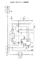
図1は従来の一例のブロック構成図を示す。
図1はノート型パーソナルコンピュータの電源供給部分の構成を示している。ACアダプタ1は、交流電源2に接続され、交流電源2から供給される交流を直流に変換する。ACアダプタ1は、電源コネクタ3に接続される。電源コネクタ3は、抵抗R1及びダイオードD1を介してDC−DCコンバータ4に接続される。
【0007】
また、DC−DCコンバータ4には、ダイオードD2を介して二次電池5が接続される。DC−DCコンバータ4は、ACアダプタ1又は二次電池5から供給された直流電源を所定の直流電圧に変換して負荷6に供給する。
また、二次電池5には、充電回路24が接続されている。充電回路24は、定電圧定電流回路8、差動増幅器9、電圧比較器10、基準電圧源12〜14、マイコン11から構成される。
【0008】
定電圧定電流回路8は、PWM制御方式で動作するスイッチングレギュレータ方式のDC−DCコンバータである。定電圧定電流回路8は、スイッチング用のメイントランジスタTr1、チョークコイルL1、フライホイールダイオードD3、平滑コンデンサC1、充電電流検出用抵抗R0、制御部7から構成される。メイントランジスタTr1はFETで構成され、制御部7によりオン・オフ制御が行われる。充電電流検出用抵抗R0は、電池5に充電される電流値を測定するためのセンス抵抗であり、センス抵抗中を流れる電流による電圧降下を制御部7に入力する。
【0009】
スイッチングレギュレータ方式のDC−DCコンバータは、スイッチング用のメイントランジスタTr1をオン・オフさせてチョークコイルL1に流れる電流を制御することで、定電圧定電流回路8のDC−DC制御を実現する。
充電電流検出用抵抗R0の両端は差動増幅器9に接続される。
差動増幅器9は、非反転入力端子が充電電流検出用抵抗R0と電池5との接続点に接続され、反転入力端子が充電電流検出用抵抗R0とチョークコイルL1との接続点に接続される。差動増幅器9は、充電電流検出用抵抗R0の両端の電圧を増幅する。差動増幅器9の出力は、電池5に供給される電流に応じた電圧となる。差動増幅器9の出力は、マイコン11に供給される。
【0010】
電圧比較器10は、非反転端子がACアダプタ1に接続され、反転端子に基準電圧源12が接続される。電圧比較器10は、ACアダプタ1の電圧に応じてハイ又はローレベルの信号を出力する。
電圧比較器10は、ACアダプタ1で発生される電圧が基準電圧源12から供給される基準電圧より大きければ出力信号をハイレベルとし、ACアダプタ1で発生される電圧が基準電圧源12から供給される基準電圧より小さくなると出力信号をローレベルにする。電圧比較器10は、ACアダプタ1が接続されると、ハイレベルになり、ACアダプタ1が接続されていないと、ローレベルになる。電圧比較器10の出力信号は、マイコン11に供給される。
【0011】
マイコン11は、差動増幅器9及び電圧比較器10の出力信号に応じて制御部7の動作を制御する。マイコン11は、差動増幅器9の出力が所定の電圧より大きければ、すなわち、充電流がながれている状態では、電池5が満充電状態にない状態であると判断する。また、マイコン11は、電圧比較器10の出力信号がローレベルであると、ACアダプタ1が接続されていると判断する。
【0012】
マイコン11は、差動増幅器9及び電圧比較器10の出力により電池5及びACアダプタ1が接続されている判断すると、電池5に充電を開始できる条件であると判断して、制御部7をオンするような制御信号を制御7に供給する。また、マイコン11は、差動増幅器9の出力信号が所定の電圧より小さい、すなわち、電池5が満充電状態である状態、又は電圧比較器10の出力信号がローレベル、すなわち、ACアダプタ1が接続されていない状態になると、電池5に充電を行えない条件であると判断して、制御部7をオフするような制御信号を制御7に供給する。
【0013】
制御部7には、マイコン11からの制御信号の他、抵抗R1の両端の電圧及び充電電流検出用抵抗R0の両端の電圧、基準電圧が供給される。制御部7は、後述するようにマイコン11からの制御信号に応じてその動作が制御され、動作時には抵抗R1の両端の電圧及び充電電流検出用抵抗R0の両端の電圧、基準電圧に応じてスイッチングトランジスタTr1のオン・オフを制御する。
【0014】
図1の回路は、負荷6に電力を供給しながら、電池5を充電回路60により、充電する。即ち、ACアダプタ1からの入力3は、DCーDC変換器4を通じて、負荷6に供給されるとともに、充電回路60を通じて、電池5にも供給される。従って、負荷6による電力消費と、電池5への充電が同時に行われる。
次に、制御部7について説明する。
【0015】
図2は従来の一例の制御部のブロック構成図を示す。
制御部7は、差動増幅器15,16、誤差増幅器17〜19、三角波発振器20、PWM比較器21、ドライバ22から構成される。
差動増幅器15は、抵抗R1の両端の電圧を検出する。差動増幅器15の出力は、抵抗R1に流れる電流、すなわち、ACアダプタ1の出力電流に応じた信号となる。
【0016】
また、差動増幅器16は、充電電流検出用抵抗R0の両端の電圧を検出する。差動増幅器16の出力は、充電電流検出用抵抗R0に流れる電流、すなわち、電池5を充電する充電電流に応じた信号となる。
差動増幅器15の出力検出信号は、誤差増幅器17の反転入力端子に供給される。誤差増幅器17の非反転入力端子には、基準電圧源13から基準電圧Vref1が印加される。誤差増幅器17は、差動増幅器15の出力と基準電圧Vref1との差分に応じた信号を出力する。基準電圧Vref1は、ACアダプタ1から供給可能な最大電流に応じて設定される。
【0017】
また、差動増幅器16の出力検出信号は、誤差増幅器18の非反転入力端子に供給される。誤差増幅器18の反転入力端子には、基準電圧源14から基準電圧Vref2が印加される。誤差増幅器18は、差動増幅器16の出力と基準電圧Vref2との差分に応じた信号を出力する。基準電圧Vref2は、電池5に供給可能な最大電流に応じて設定される。
【0018】
誤差増幅器19は、反転入力端子が充電電流検出用抵抗R0と電池5との接続点に接続され、非反転入力端子には基準電圧源23が印加される。誤差増幅器19の出力は、充電電流検出用抵抗R0と電池5との接続点、すなわち、電池5の充電電圧と基準電圧源23の基準電圧Vref3との差分を出力する。誤差増幅器19の出力は、PWM比較器21に供給される。基準電圧Vref3は、電池5に印加可能な最大電圧に応じて設定される。
【0019】
三角波形発振器20は、出力レベルがのこぎり波状に変化する信号を出力する。三角波形発振器20で生成された信号は、PWM比較器21に供給される。
PWM比較器21は、誤差増幅器17,18,19の出力のそれぞれと三角波形発振器20で生成されたのこぎり波信号とを比較し、その大小関係に応じてハイレベル又はローレベルとなる信号をそれぞれで生成し、そのAND論理に応じた出力パルスする。PWM比較器20の出力パルスは、ドライバ22に供給される。ドライバ22は、PWM比較器20の出力パルスに応じてスイッチングトランジスタTr1をオン・オフする。
【0020】
図3は従来の一例の動作説明図を示す。図3(A)は三角波形及び誤差増幅器17〜19の出力の波形、図3(B)はスイッチングトランジスタTr1のオン・オフの状態を示す。
図3(A)に示すように誤差増幅器17〜19の出力のうち最小の電圧レベルがPWM比較器21により三角波発振器20から供給されるのこぎり波と比較される。誤差増幅器17〜19の出力のうち最小の電圧レベルが三角波発振器20から供給されたのこぎり波より大きいときに、図3(B)に示すようにスイッチングトランジスタTr1がオンし、その他の期間ではスイッチングトランジスタTr1はオフする。
【0021】
スイッチングトランジスタTr1がオン・オフされることにより、スイッチングトランジスタTr1からはパルス状に電流が出力される。スイッチングトランジスタTr1から出力された電流は、整流回路8により整流されて直流とされて、電池5に供給される。このとき、電池5に供給される電圧、電流は、スイッチングトランジスタTr1のオン・オフの期間によって制御される。いわゆる、PWM制御される。
【0022】
図2の誤差増幅器17は、差動増幅器15の出力と図1に示される基準電圧源13から供給されるDC−CURR(基準電圧Vref1)とを差動増幅する。前述した通り、図1に示される基準電圧源13から供給されるDC−CURR(基準電圧Vref1)は、ACアダプタ1 の供給可能な最大電流値にあわせて設定されるリファレンスである。従って誤差増幅器17の出力は、ACアダプタ1 が、負荷6及び電池5に流す電流の和が、ACアダプタ1の供給可能な最大電流値となるよう、PWM比較器21を通じて、ドライバ22を動かす。
【0023】
即ち、誤差増幅器17は、装置が動作しているときは(負荷6に、ACアダプタ1に電力が供給されているときは)、負荷6の消費電力の増減に応じて電池5の充電電流を増減させ、負荷6の消費電流と電池5の充電電流の合計がACアダプタ1の最大電力容量となるように充電電流を制御する。この場合、負荷6の消費電流が増加した場合、センス抵抗R1に流れる電流が増え、差動増幅器15の出力が大となり、図1に示される基準電圧源13から供給されるDC−CURR(基準電圧Vref1)とACアダプタ1の出力電流との誤差が小さくなるものと、三角波発振器20の出力とを比較し、ドライバ22を動かす。
【0024】
負荷6の消費電流が増加した場合は、誤差増幅器17の出力が他の誤差増幅器18,19に比較して小さくなるので、誤差増幅器17による制御により、電池5の充電が制御されることになる。すなわち、充電電流が押さえられることになる。
図2の誤差増幅器18は、図1のセンス抵抗R0に流れる電流値に対応する差動増幅器16の値と、図1に示す基準電圧源14の出力基準電圧Vref2であるBAT CURRは、電池5が許容できる最大充電電流を定めているので、誤差増幅器18の出力は、電池5が所定充電電流で充電されるように制御するためのものである。
【0025】
誤差増幅器19は、電池5の充電電圧ERR2−と基準電圧源23で発生される基準電圧Vref3との誤差を増幅している。なお、基準電圧源23で発生される基準電圧Vref3は、電池5に印加可能な最大電圧に応じて設定される。従って、誤差増幅器19の出力は、電池5が印加可能な最大電圧レベルとなるように、ドライバ22を起動するためのものである。
【0026】
上記のように、PWM比較器21は、非反転入力端子に誤差増幅器17,18,19が入力されている。従って、図3(A)に示すように誤差増幅器17,18,19の最小の電圧レベルにより、スイッチングトランジスタTr1のオン・オフが制御されることになる。
従って、誤差増幅器18の出力が最小電圧レベルのときは、電池5への電力が定電流になるように、スイッチングトランジスタTr1がオン・オフされる。DC−DC変換の分野(又は、DC−DC変換の制御回路の分野)では、図2に示す誤差増幅器18,16等により、電池5への充電電流が定電流になることから、充電電流を定電流に制御する回路を定電流回路と称している。また、定電流制御回路や定電流充電制御回路と称されることもある。この定電流充電については図5でさらに詳細に説明する。
【0027】
誤差増幅器19の出力が最小電圧レベルのときは、電池5に印加される電圧が定電圧になることから、充電電圧を定電圧に制御する回路を、定電圧回路と称している。また、定電圧制御回路や定電圧充電制御回路と称されることもある。この定電圧充電については、図5でさらに詳細に説明する。
また、このような、定電流回路と定電圧回路の両方を持つ回路、又は、両方の機能(もしくは、それと等価の機能)の回路を、DC−DC変換器の制御回路の技術分野では、定電圧定電流制御回路(又は、定電流定電圧回路)と称している。
【0028】
次にマイコン11の動作について説明する。
図4は従来の一例のマイコンのフローチャートを示す。
マイコン11は、充電開始条件か否かを判断する(ステップS1−1)。ステップS1−1の開始条件は、ACアダプタ1から電圧が供給されていること、及び、電池5が接続されていること、並びに、電池5が満充電状態ではないことである。
【0029】
マイコン11は、充電開始条件のうちACアダプタ1から電圧が供給されている点については、電圧比較器10の出力がハイレベルであることによって判断する。また、マイコン11は、電池5が満充電状態ではないことについては、差動増幅器9の出力が所定レベル以上か否かを検出することにより検出される。すなわち、満充電でない状態では、充電電流検出用抵抗R0に電流が流れることになるので、充電電流検出用抵抗R0の両端に電圧が発生し、差動増幅器9の出力が所定レベル以上となる。
【0030】
マイコン11はステップS1−1で充電開始条件になると、制御部7をオンにする(ステップS1−2)。制御部7はマイコン11により動作がオンされると、抵抗R1及び充電電流検出用抵抗R0の両端の電圧に応じて電池5に供給する電流をPWM制御する。
マイコン11は、充電中に充電電流が規定値以下になったか否かを判断する(ステップS1−3)。充電電流が規定値以下になったか否かは、差動増幅器9の出力信号を検出することにより判定される。すなわち、充電電流が規定値以下になると、充電電流検出用抵抗R0の両端に電圧が低下し、差動増幅器9の出力が小さくなるので、差動増幅器9の出力を検出することにより検出可能となる。
【0031】
ステップS1−3で、充電電流が規定値以下でなければ、そのまま充電を続ける。また、ステップS1−3で、充電電流が規定値以下になった場合には、電池5への充電は完了したと判断して、制御部7の動作を停止させ、電池5への充電を停止させる。
次に、電池5の充電動作について説明する。
【0032】
図5は電池の充電特性を示す図である。図5(A)は電池5の充電電圧、図5(B)は電池5の充電電流の特性を示す。
図5(A)に示すように時刻t1で電池5が定電圧状態となったとすると、時刻t1以降、図5(B)に示すように充電電流Iが低下する。充電電流Iが低下し、図5(B)に示すように時刻t2で所定値I0以下になると、マイコン11により制御部7の動作が停止され、電池5への充電が停止される。
【0033】
この図5の動作を図1,2を用いて説明する。
負荷6に大きな電流が流れていないと仮定すると、制御部( 図2)は、3つの誤差増幅器17〜19のうち誤差増幅器17の出力が最小にはならないので、誤差増幅器18又は誤差増幅器19のいずれかの出力で、充電が制御される。図5において、充電の開始時においては、電池5(特に、リチウム電池の場合)は、図2の誤差増幅器18の出力が、他の正の入力にくらべて小さくなる。従って、電池5は、図5(B)の時刻t1までは、定電流で充電されるように、制御部7は制御する。即ち、充電の初期においては、誤差増幅器18により、基準電圧源14で発生される基準電圧Vref2であるBAT CURRに対応する電流値で、充電する。
【0034】
その間、図5(A)に示すように、電圧が上昇し、所定電圧に達したとき(時刻t1)、図2の誤差増幅器19の出力電圧が最小となり、充電は誤差増幅器19の出力で制御される。従って、時刻t1以降は、電池5に印加電圧が定電圧になるように制御される。時刻t1以降は、前述した通り、充電電流は徐々に低下する。DC−DC変換器の分野では(又は、DC−DC変換器の制御回路の分野では)、図2の誤差増幅器18,誤差増幅器16等により、電池への充電電流が定電流になることから、充電電流を定電流に制御する回路を、定電流回路と称している。又、定電流制御回路や定電流充電制御回路と称されることもある。更に、DC−DC変換器の分野では(又は、DC−DC変換器の制御回路の分野では)、図2の誤差増幅器19等により、電池への充電電圧が定電圧になることから、充電電圧を定電圧に制御する回路を、定電圧回路と称している。又、定電圧制御回路や定電圧充電制御回路と称されることもある。
【0035】
図2の制御回路は、図5の充電特性図で説明した通り、定電流充電と定電圧充電の両方を行う。このような、図2のように、定電流回路と定電圧回路の両方を持つ回路、又は、両方の機能(もしくは、それと等価の機能)の回路を、DC−DC変換器の制御回路の技術分野では、定電圧定電流回路( 又は、定電流定電圧回路) と称している。
【0036】
なお、上記の構成の充電制御回路については、特開平8−182219号に詳細に記載されている。
【0037】
【発明が解決しようとする課題】
しかるに、従来の充電回路では、上記のようにACアダプタ1の電圧及び電池5に供給される電流に応じても制御部7によるスイッチングトランジスタTr1の動作を制御していた。このとき、電池5が満充電状態ではない状態で、負荷6での消費電流が増大し、ACアダプタ1の供給限界の電流を越えた場合には、ACアダプタ1の出力電流はほとんどが抵抗R1、ダイオードD1、DC−DCコンバータ4を介して負荷6に供給される。
【0038】
即ち、ACアダプタ1は、電池5に接続されるとともに、負荷6にも接続されている。電池5の充電は、負荷6がオン(電力を消費するとき)のときも、行うことができる。その際には、ACアダプタ1の電力は、電池5の充電と、負荷6への供給の両方に使用される。負荷6の消費電力があまり大きくない時は、図5の特性で、電池5を充電できる。しかし、負荷6での消費電流が増大し、ACアダプタ1の供給限界の電流を超えたときは、図2の誤差増幅器17の出力により、スイッチングトランジスタTr1が制御されることとなり、充電回路6には、電流があまり供給されなくなる。これは、前述した通り、誤差増幅器17は、ACアダプタ1が、負荷6及び電池5に流す電流の和が、ACアダプタ1の供給可能な最大電流値となるよう、PWM比較器21を通じて、ドライバ22を動かす。即ち、誤差増幅器17は、装置が動作しているときは(負荷6に、ACアダプタ1に電力が供給されているときは)、負荷6の消費電力の増減に応じてACアダプタ1の電流が負荷6に供給されることになり、充電回路6には電流が供給されなくなる。このため、充電電流検出用抵抗R0に電流が流れなくなり、充電電流検出用抵抗R0の電圧が低下する。充電電流検出用抵抗R0の電圧が低下すると、マイコン11は充電が完了したと判断するので、制御部7の動作を停止してしまう。
【0039】
このような状況は、ACアダプタの容量が充分でない場合に、起こりやすい。 又、ノートパソコン等の電子機器に複数の二次電池が搭載されている場合、1 ケの充電回路で複数の二次電池を同時に充電する並列充電も行われる。並列充電において、複数の電池パック間で残量が異なる場合、最も残量の少ない電池パックに充電電流が流れ、残量の多い電池パックには少ない充電電流しか流れないかあるいは、充電電流が全く流れないこともあり得る。このような場合においても特定の電池パックの充電電流が極端に少なくなったことで充電電流が全く流れない事もあり得る。このような場合においても特定の電池パックの充電電流が極端に少なくなったことで充電完了を誤認識する可能性がある。
【0040】
並列充電に於いて、複数の電池パック間で残量が異なる場合、最も残量の少ない電池パックに充電電流が流れ、残量の多い電池パックには少ない充電電流しか流れないか或いは、充電電流が全く流れないこともあり得る。このような場合に於いても特定の電池パックの充電電流が極端に少なくなったことで充電完了を誤認識する可能性がある。
【0041】
以上のように、電池5が満充電状態でないにもかかわらず制御部7の動作が停止してしまい、充電動作が停止されてしまう等の問題点があった。
また、以上述べたように、ノートパソコン等の電子機器の為の充電器で電池を充電する場合、出来る限り短時間の間に充電を行うような各種手法の実現に当たって、必ずしも二次電池が要求する電流での充電を行うことが出来ない場合が生じる。しかし、Li+電池のように充電電流が一定値以下に成ったことで充電完了を検出する方式では、このように装置側の都合によって二次電池の充電電流が極端に少なく成った場合、充電完了と誤認識する問題があった。
【0042】
そこで、本特許に於いては上記問題点を鑑み、充電用の定電圧定電流制御回路に於いて、充電電流の制限条件が電池の受入れ能力で制限されているのか、充電器側の都合で制限しているのかを識別するための信号を出力させることで、充電完了の誤検出を防止するようにした充電制御方式を提案するものである。又、本発明は充電回路の誤作動を防止できる充電制御回路及び充電装置並びに充電制御方法を提供することを目的とする。
【0043】
【課題を解決するための手段】
本発明は、電源から電池を充電する充電電流を制御する充電装置において、電池が所定の充電特性に応じて充電されるように前記電池への充電を制御する第1の制御回路と、電源からの電力供給が所定の制限を超えないように充電を制御する第2の制御回路と、第1の制御回路により電池の充電が制御されているのか、第2の制御回路により電池の充電が制御されているのかを判別する判別手段と、電池の充電状態を検出する検出手段と、判別手段の判別結果が前記第2の制御回路により前記電池の充電が制御されていないことを示し、かつ、前記検出手段の検出結果が前記電池の満充電状態を示す場合に充電の完了を判定する手段とを有することを特徴とする。
また、本発明は、電源から、電池への充電と負荷への電力供給を同時に行うよう充電を制御する充電装置において、電池が所定の充電特性に応じて充電されるように前記電池への充電を制御する第1の制御回路と、電源からの電力供給が所定の制限を超えないように充電を制御する第2の制御回路と、第1の制御回路により電池の充電が制御されているのか、第2の制御回路により電池の充電が制御されているのかを判別する判別手段と、電池の充電状態を検出する検出手段と、前記判別手段の判別結果が前記第2の制御回路により前記電池の充電が制御されていないことを示し、かつ、前記検出手段の検出結果が前記電池の満充電状態を示す場合に充電の完了を判定する手段とを有することを特徴とする。
【0044】
本発明によれば、前記判別手段の判別結果が前記第2の制御回路により前記電池の充電が制御されていないことを示し、かつ、前記検出手段の検出結果が前記電池の満充電状態を示す場合に充電の完了を判定することにより、電源の供給能力が制限状態で、負荷に電流が供給され、電池の充電電流が低下したときに、電池の充電が完了したと誤検出するようなことがなくなる。
【0051】
【発明の実施の形態】
図6は本発明の第1実施例のブロック構成図を示す。同図中、図1と同一構成部分には同一符号を付し、その説明は省略する。
本実施例は、図1とは充電回路の構成が相違する。
本実施例の充電回路30は、スイッチングトランジスタTr1、チョークコイルL1、ダイオードD3、コンデンサC1、充電電流検出用抵抗R0とともに定電圧定電流回路を構成する制御部31の構成及びマイコン32の処理が相違する。
【0052】
本実施例の制御部31は、ACアダプタ1の出力電流及び電池5の充電電流並びに電池5の充電電圧に基づいて充電電流の制限条件が電池5の受け入れ能力で制限されているのか(負荷6の消費電流が増加して電池5への充電電流が制限されているのか)、充電器30の検出状態により制限されているかを識別するための識別信号を出力する。マイコン32は、制御部31からの識別信号に基づいて制御部31の動作を制御する。
【0053】
図7は本発明の第1実施例の制御部のブロック構成図を示す。同図中、図2と同一構成部分には同一符号を付し、その説明は省略する。
制御部31は、誤差増幅器17の出力と誤差増幅器18,19の出力とを比較する電圧比較器33を有する。制御部31は、例えば、1チップのICから構成されており、入力端子T1〜T6及び出力端子T7,T8を有する。入力端子T1 は制御部31の外部で抵抗R1とコネクタ3との接続点に接続され、制御部31の内部で差動増幅器15の非反転入力端子に接続される。入力端子T2は制御部31の外部で抵抗R1とダイオードD1との接続点に接続され、制御部31の内部で差動増幅器15の反転入力端子に接続される。
【0054】
入力端子T3は制御部31の外部で基準電圧源13に接続され、制御部31の内部で誤差増幅器17の非反転入力端子に接続される。入力端子T4は制御部31の外部でチョークコイルL1と充電電流検出用抵抗R0との接続点に接続され、制御部31の内部で差動増幅器16の非反転入力端子に接続される。
入力端子T5は制御部31の外部で充電電流検出用抵抗R0と電池5との接続点に接続され、制御部31の内部で差動増幅器16、誤差増幅器19の反転入力端子に接続される。入力端子T6は制御部31の外部で基準電圧電源14に接続され、制御部31の内部で誤差増幅器18の非反転入力端子に接続される。
【0055】
さらに、出力端子T7は制御部31の外部でマイコン32に接続され、制御部31の内部でドライバ22に接続される。出力端子T8は制御部31の外部でマイコン32に接続され、制御部31の内部で電圧比較器33に接続される。
電圧比較器33は3入力の比較器を構成しており、反転入力端子に誤差増幅器17の出力が供給され、2つの非反転入力端子に誤差増幅器18,19の出力が供給される。
【0056】
電圧比較器33は、誤差増幅器18,19の出力を誤差増幅器17の出力と比較する。電圧比較器33は、誤差増幅器18,19の出力のいずれか一方が誤差増幅器17の出力より大きい状態、すなわち、通常の充電状態ではありえない出力関係になるとハイレベルとなり、誤差増幅器18,19の出力の両方とも誤差増幅器17の出力より小さい状態、すなわち、通常の充電状態での出力関係になるとローレベルとなる出力信号を出力する。電圧比較器33の出力がハイレベルの状態では、誤差増幅器17の出力、すなわち、ACアダプタ1の出力電流によってPWM比較器21が制御された状態であり、
マイコン32は、電圧比較器33の出力信号がローレベルのときには、差動増幅器9及び電圧比較器10の出力に応じて制御部31の動作をオン・オフし、電圧比較器33の出力信号がハイレベルのときには、差動増幅器9及び電圧比較器10の出力によらず、制御部31をオンに維持する。
【0057】
図8は本発明の第1実施例のマイコンのフローチャートを示す。
マイコン32は、まず、図4のステップS1−1と同様に充電開始条件か否かを判断する(ステップS2−1)。
マイコン32はステップS2−1で充電開始条件になると、制御部31をオンにする(ステップS2−2)。制御部31はマイコン32により動作がオンされると、抵抗R1及び充電電流検出用抵抗R0の両端の電圧に応じて電池5に供給する電流をPWM制御する。
【0058】
マイコン32は、充電中に充電電流が規定値以下になったか否かを判断する(ステップS2−3)。充電電流が規定値以下になったか否かは、差動増幅器9の出力信号を検出することにより判定される。すなわち、充電電流が規定値以下になると、充電電流検出用抵抗R0の両端に電圧が低下し、差動増幅器9の出力が小さくなるので、差動増幅器9の出力を検出することにより検出可能となる。
【0059】
ステップS2−3で、充電電流が規定値以下でなければ、そのまま充電を続ける。また、ステップS2−3で、充電電流が規定値以下になった場合には、次にACアダプタ1が電流制限を行っているか否かを判断する(ステップS2−4)。
ステップS2−4のACアダプタ1で電流制限を行っているか否かの判断は、出力端子T8から出力される信号に応じて判定される。すなわち、マイコン32は、電圧比較器33の出力がハイレベルであれば、電流制限が行われていると判断する。
【0060】
ステップS2−4でACアダプタ1が電流制限を行っている、すなわち、制御部31の出力端子T8の出力信号がハイレベルの時には、ステップS2−3に戻って制御部31の動作をそのまま続行させる。
また、ステップS2−4でACアダプタ1が電流制限を行っていない、すなわち、制御部31の出力端子T8の出力信号がローレベルの時には、電池5が満充電状態になったと判断して、制御部31の動作を停止させ、電池5の充電を終了させる。
【0061】
以上のように、負荷6での消費電流の増大によりACアダプタ1に電流制限が生じても、電池5の充電電流の低減及び充電電圧の低下により、制御部31の動作を停止させずに、電池5が満充電ではないと判断して、制御部31の動作を続行することにより、負荷6の消費電流が低減したときに再び電池5に充電が行われる。よって、電池5を確実に満充電状態にすることができる。
【0062】
なお、本実施例では、ACアダプタ1での電流制限の発生を誤差増幅器17〜19の出力を電圧比較器33により比較することにより検出したが、これに限られるものではなく、誤差増幅器18,19の出力を予め設定された基準電圧と比較することにより検出してもよい。
図9は本発明の第1実施例の制御部のブロック構成図を示す。同図中、図7と同一構成部分には同一符号を付しその説明は省略する。
【0063】
本変形例の制御部40は、電圧比較器33の2つの非反転入力端子に誤差増幅器18,19の出力を供給し、反転入力端子に基準電圧源42から基準電圧Vref4を供給する。
電圧比較器33は、誤差増幅器18,19の出力と基準電圧源42で生成された基準電圧Vref4とを比較する。電圧比較器33は、誤差増幅器18,19の出力が基準電圧源42で生成された基準電圧Vref4より小さければ、ローレベル、誤差増幅器18,19の出力が基準電圧源42で生成された基準電圧Vref4より大きければ、ハイレベルとなる出力信号を出力端子T8から出力する。
【0064】
基準電圧源42で発生される基準電圧Vref4を三角波発振器20で発生されるノコギリ波の最大値より大きく設定することにより、誤差増幅器18,19の出力が制御範囲外にあることを検出できる。
電池5に供給される電流はACアダプタ1の電力供給能力が制限状態にあるときには電池5の供給する電流より小さくなるため、誤差増幅器18,19の出力は制御範囲越える。よって、三角波発振器20で生成されるノコギリ波より大きい値に基準電圧Vref4を設定しておき、誤差増幅器18,19の出力が基準電圧Vref4を越えたことを検出することによりACアダプタ1の電力供給能力が制限状態にあることを検出できる。
【0065】
なお、本実施例では、誤差増幅器18,19の出力、すなわち、充電電流、充電電圧の誤差値を基準電圧Vref4と比較することによりACアダプタ1が電流制限状態にあることを検出したが、これに限られるものではなく、ACアダプタ1の出力電流を検出することによりACアダプタ1の電流制限状態を検出するようにしてもよい。
【0066】
図10は本発明の第1実施例の制御部の第2変形例のブロック構成図を示す。同図中、図7と同一構成部分には同一符号を付し、その説明は省略する。
本変形例の制御部50は、3入力電圧比較器33及び基準電圧源42に代えて2入力電圧比較器51及び基準電圧源52を設けてなる。2入力電圧比較器51の反転入力端子には誤差増幅器17の出力が供給され、2入力電圧比較器51の非反転入力端子には基準電圧源52で発生した基準電圧Vref5が供給される。
【0067】
入力電圧比較器51は、誤差増幅器17の出力と基準電圧Vref5とを比較する。入力電圧比較器51は、誤差増幅器17の出力が基準電圧Vref5より大きければローレベル、誤差増幅器17の出力が基準電圧Vref5より小さければハイレベルの信号を出力する。
すなわち、ACアダプタ1の出力電流が増加し、ACアダプタ1が電力供給能力の制限値に近づくと、誤差増幅器17の出力が低下する。誤差増幅器17の出力が低下し、基準電圧Vref5より小さくなると、電圧比較器51の出力信号がハイレベルになり、ACアダプタ1の出力電流が制限されていることを検出できる。
【0068】
なお、上記第1実施例では、ACアダプタ1の電流を抵抗R1の両端の電圧から検出し、制御部31,40,50の制御を行ったが、ACアダプタ1の電圧により制御部を制御するようにしてもよい。
図11は本発明の第2実施例のブロック構成図を示す。同図中、図6と同一構成部分には同一符号を付し、その説明は省略する。
【0069】
本実施例の電源装置60は、ACアダプタ1の出力電流を検出するための抵抗R1がないとともに、充電回路61の構成が第1実施例とは相違する。ACアダプタ1の出力電流は、ダイオードD1を介してDC−DCコンバータ4に供給される。
本実施例の充電回路61は、制御部62の構成が第1実施例とは相違する。本実施例の制御部62は、ACアダプタ1の出力電圧及び電池の充電電流並びに充電電圧を検出し、スイッチングトランジスタTr1を制御する。
【0070】
図12は本発明の第2実施例の制御部のブロック構成図を示す。同図中、図7と同一構成部分には同一符号を付し、その説明は省略する。
本実施例の制御部62は、差動増幅器16、誤差増幅器18〜19,63、三角波発振器20、PWM比較器21、ドライバ22、基準電圧源23,64から構成される。
【0071】
入力端子T2にACアダプタ1の出力電圧が印加される。入力端子T2には、誤差増幅器63の非反転入力端子が接続される。誤差増幅器63の反転入力端子には基準電圧源64が接続される。
誤差増幅器63は、ACアダプタ1の出力電圧と基準電圧源64で発生される基準電圧Vref6との差動信号を出力する。誤差増幅器63の出力は3入力電圧比較器33の反転入力端子に供給される。3入力電圧比較器33は、非反転入力端子に誤差増幅器18,19の出力が供給されている。3入力電圧比較器33は、誤差増幅器18,19の出力と差動増幅器23の出力とを比較する。
【0072】
3入力電圧比較器33は、誤差増幅器18,19の出力がともに誤差増幅器63の出力より小さければローレベル、誤差増幅器18,19のいずれかの出力が誤差増幅器63の出力より大きければハイレベルの信号を出力する。
誤差増幅器18,19の出力がともに誤差増幅器63の出力より小さい状態では、通常の動作が行われていると判断できる。また、誤差増幅器18,19の出力のいずれかが誤差増幅器63の出力より大きい状態では、ACアダプタ1の出力電流が制限されていると判断できる。
【0073】
よって、3入力電圧比較器33の出力をマイコン32に供給し、マイコン32で、図8に示すような処理を行うことによりACアダプタ1の電力供給能力による電流制限により制御部62の動作が停止されることはない。
なお、本変形例では3入力電圧比較器33により誤差増幅器18,19の出力と誤差増幅器63の出力とを比較したが、誤差増幅器18,19の出力を予め設定された基準電圧と比較するようにしてもよい。
【0074】
図13は本発明の第2実施例の制御部の第1変形例のブロック構成図を示す。同図中、図12と同一構成部分には同一符号を付し、その説明は省略する。
本変形例の制御部70は電圧比較器33の反転入力端子に誤差増幅器63の出力に代えて基準電圧源71を接続してなる。
電圧比較器33は、誤差増幅器18,19の出力が基準電圧源71で生成された基準電圧Vref7より小さければローレベル、誤差増幅器18,19の出力のいずれかが基準電圧源71で生成された基準電圧Vref7より大きければハイレベルの出力信号を出力する。
【0075】
誤差増幅器18,19の出力がともに基準電圧源71で生成された基準電圧Vref7より小さい状態では、通常の動作が行われていると判断できる。また、誤差増幅器18,19の出力のいずれかが基準電圧源71で生成された基準電圧Vref7より大きい状態では、ACアダプタ1の出力電流が制限されていると判断できる。
【0076】
よって、3入力電圧比較器33の出力をマイコン32に供給し、マイコン32で、図8に示すような処理を行うことによりACアダプタ1の電流制限により制御部70の動作が停止されることはない。
なお、本変形例では3入力電圧比較器33により誤差増幅器18,19の出力と基準電圧源71で生成された基準電圧Vref7とを比較したが、誤差増幅器63の出力を予め設定された基準電圧と比較するようにしてもよい。
【0077】
図14は本発明の第2実施例の制御部の第2変形例のブロック構成図を示す。同図中、図13と同一構成部分には同一符号を付し、その説明は省略する。
本変形例の制御部80は3入力電圧比較器33に代えて2入力電圧比較器81を設け、2入力電圧比較器81の反転端子に誤差増幅器63の出力を供給し、非反転入力端子に基準電圧源81を接続してなる。
【0078】
電圧比較器81は、誤差増幅器63の出力が基準電圧源82で生成された基準電圧Vref8より小さければローレベル、誤差増幅器63の出力が基準電圧源82で生成された基準電圧Vref8より大きければハイレベルの出力信号を出力する。 誤差増幅器63の出力が基準電圧源81で生成された基準電圧Vref8より小さい状態、すなわち、誤差が小さい状態では、通常の動作が行われていると判断できる。また、誤差増幅器63の出力が基準電圧源82で生成された基準電圧Vref8より大きい状態、すなわち、誤差が大きい状態では、ACアダプタ1の出力電流が制限されていると判断する。
【0079】
よって、2入力電圧比較器81の出力をマイコン32に供給し、マイコン32で、図8に示すような処理を行うことによりACアダプタ1の電力供給能力が制限状態になることにより制御部80の動作が停止されることはない。
なお、第1及び第2実施例では、電池5の充電を制御する場合について説明したが、電池が並列に複数ある場合についても適用することができる。
【0080】
図15は本発明の第3実施例のブロック構成図を示す。同図中、図6と同一構成部分には同一符号を付し、その説明は省略する。
本実施例の電源装置90は、電池91,92が並列に接続され、充電回路93は、電池91,92に並列に充電を行う。
充電回路93は、スイッチングトランジスタTr1、制御部94、チョークコイルL2、フライホールダイオードD3、平滑コンデンサC1、充電電流検出用抵抗R11,R12、差動増幅器9,106,107、電圧比較器10、マイコン11、基準電圧源12,95,96、ダイオードD11〜D14、から構成される。
【0081】
充電電流検出用抵抗R11は、電池91の充電電流を検出する。充電電流検出用抵抗R12は、電池92の充電電流を検出する。ダイオードD11〜D14は電池91,92を保護する。
【0082】
充電電流検出用抵抗R12は、制御部94に接続されるとともに、差動増幅器107に接続される。差動増幅器107は充電電流検出用抵抗R11の両端の電位差に応じた出力をマイコン11に供給する。
制御部94は、ACアダプタ1の出力電流、充電電流検出用抵抗R11,R12により検出される電池91,92の充電電流に応じてスイッチングトランジスタTr1を制御する。
【0083】
ここで、制御部94について詳細に説明する。
図16は本発明の第3実施例の制御部のブロック構成図を示す。同図中、図7と同一構成部分には同一符号を付し、その説明は省略する。
本実施例の制御部94は、差動増幅器15,97,98、誤差増幅器17,99〜102、三角波発振器20、ドライバ22、基準電圧源103、PWM比較器104、電圧比較器105から構成される。
【0084】
制御部94には、入力端子T1〜T3、T11〜T16及び出力端子T7,T8を有する。入力端子T1,T2は抵抗R1の両端に接続され、入力端子T3は基準電圧源13が接続される。また、入力端子T11,T12には抵抗R11の両端が接続され、入力端子T14,T14には抵抗R12の両端が接続される。さらに、入力端子T15には基準電圧源95、入力端子T16には基準電圧源96が接続される。さらに、出力端子T7,T8はマイコン32に接続される。
【0085】
入力端子T11には、差動増幅器97の非反転入力端子が接続され、入力端子T12には、差動増幅器97及び誤差増幅器101の反転入力端子が接続される。差動増幅器97は、抵抗R11の両端の電圧、すなわち、電池91の充電電流に応じた信号を出力する。
入力端子T13には、差動増幅器98の非反転入力端子が接続され、入力端子T14には、差動増幅器98及び誤差増幅器102の反転入力端子が接続される。差動増幅器98は、抵抗R12の両端の電圧、すなわち、電池92の充電電流に応じた信号を出力する。
【0086】
誤差増幅器101,102の非反転入力端子には、基準電圧源103が接続される。誤差増幅器101は、電池91の充電電圧と基準電圧源103で発生される基準電圧との差動信号を出力する。誤差増幅器102は、電池92の充電電圧と基準電圧源103で発生される基準電圧との差動信号を出力する。
差動増幅器97の出力は誤差増幅器99の反転入力端子に供給される。誤差増幅器99の非反転入力端子は、入力端子T15に接続される。誤差増幅器99は、差動増幅器97の出力と基準電圧源95で発生される基準電圧との差動信号を出力する。
【0087】
差動増幅器98の出力は誤差増幅器100の反転入力端子に供給される。誤差増幅器100の非反転入力端子は、入力端子T16に接続される。誤差増幅器100は、差動増幅器98の出力と基準電圧源96で発生される基準電圧との差動信号を出力する。
誤差増幅器17、99,100,101,102の出力は、PWM比較器104の非反転入力端子に供給される。PWM比較器104の反転入力端子には、三角波発振器20の出力が供給される。
【0088】
PWM比較器104は、誤差増幅器17、99,100,101,102の出力のそれぞれと三角波発振器20の出力とを比較し、その比較結果のAND論理を出力する。誤差増幅器17、99,100,101,102の出力のそれぞれと三角波発振器20の出力との比較結果は、誤差増幅器17、99,100,101,102の出力が三角波発振器20の出力より大きいときにハイレベル、誤差増幅器17、99,100,101,102の出力が三角波発振器20の出力より小さいときにローレベルとなる信号を出力する。
【0089】
また、誤差増幅器99,100,101,102の出力は電圧比較器105の非反転入力端子に供給され、誤差増幅器17の出力は電圧比較器105の反転入力端子に供給される。
電圧比較器105は、非反転入力端子に供給される誤差増幅器99,100,101,102の出力と反転入力端子に供給される誤差増幅器17の出力とを比較し、その比較結果を出力する。電圧比較器105は、誤差増幅器99,100,101,102の出力が差動増幅器17の出力より小さいときにローレベル、誤差増幅器99,100,101,102の出力のいずれかが誤差増幅器17の出力より大きいときにハイレベルとなる出力信号を出力する。
【0090】
ACアダプタ1が通常の状態で動作しているときには、ACアダプタ1の出力電流と制限電流との誤差が大きく、誤差増幅器17の出力は大きくなり、逆に、電池91,92を充電すべき電流と実際に供給されている電流との誤差は小さいので電圧比較器105の出力はローレベルとなる。
また、ACアダプタ1の電力供給能力が制限状態になると、ACアダプタ1の出力電流と制限電流との誤差は小さくなり、誤差増幅器17の出力は小さくなり、逆に、負荷6に電流が供給され、電池91,92に電流が供給されなくなるので、電池91,92を充電すべき電流と実際に供給されている電流との誤差は大きくなるので電圧比較器105の出力はハイレベルとなる。
【0091】
以上によりACアダプタ1の電流制限状態を検出できる。よって、マイコン32により電流比較器105の出力に応じて図8に示すような処理を行うことにより、誤動作を防止できる。
なお、本実施例では、誤差増幅器99,100,101,102の出力と誤差増幅器17の出力との大小を比較することによりACアダプタ1の電流制限状態を検出したが、これに限られるものではなく、誤差増幅器99,100,101,102の出力を予め設定された基準電圧と比較することによりACアダプタ1の電流制限状態を検出するようにしてもよい。すなわち、ACアダプタ1の電力供給能力が制限されていることを検出できればよい。
【0092】
図17は本発明の第3実施例の制御部の第1変形例のブロック構成図を示す。同図中、図16と同一構成部分には同一符号を付し、その説明は省略する。
本変形例の制御部110は、電圧比較器105の4つの非反転入力端子に誤差増幅器99,100,101,102の出力を供給し、反転入力端子に基準電圧源111から基準電圧Vref11 を供給する。
【0093】
電圧比較器105は、誤差増幅器99,100,101,102の出力と基準電圧源111で生成された基準電圧Vref11 とを比較する。電圧比較器105は、誤差増幅器99,100,101,102の出力が基準電圧源111で生成された基準電圧Vref11 より小さければ、ローレベル、誤差増幅器99,100,101,102の出力のいずれかが基準電圧源111で生成された基準電圧Vref11 より大きければ、ハイレベルとなる出力信号を出力端子T8から出力する。
【0094】
基準電圧源111で発生される基準電圧Vref11 を三角波発振器20で発生されるノコギリ波の最大値より大きく設定することにより、誤差増幅器99,100,101,102の出力が制御範囲外にあることを検出できる。
電池91,92に供給される電流はACアダプタ1が電流制限状態にあるときには電池91,92の供給する電流より小さくなるため、誤差増幅器99,100,101,102の出力は制御範囲越える。よって、三角波発振器20で生成されるノコギリ波より大きい値に基準電圧Vref11 を設定しておき、誤差増幅器99,100,101,102の出力が基準電圧Vref11 を越えたことを検出することによりACアダプタ1が電流制限状態にあることを検出できる。
【0095】
なお、本実施例では、誤差増幅器99,100,101,102の出力、すなわち、充電電流、充電電圧の誤差値を基準電圧Vref11 と比較することによりACアダプタ1が電流制限状態にあることを検出したが、これに限られるものではなく、ACアダプタ1の出力電流を検出することによりACアダプタ1の電力供給能力の制限状態を検出するようにしてもよい。
【0096】
図18は本発明の第3実施例の制御部の第2変形例のブロック構成図を示す。同図中、図17と同一構成部分には同一符号を付し、その説明は省略する。
本変形例の制御部120は、5入力電圧比較器105及び基準電圧源111に代えて2入力電圧比較器121及び基準電圧源122を設けてなる。2入力電圧比較器121の反転入力端子には誤差増幅器17の出力が供給され、2入力電圧比較器121の非反転入力端子には基準電圧源122で発生した基準電圧Vref12 が供給される。
【0097】
入力電圧比較器121は、誤差増幅器17の出力と基準電圧Vref12 とを比較する。入力電圧比較器121は、誤差増幅器17の出力が基準電圧Vref12 より大きければローレベル、誤差増幅器17の出力が基準電圧Vref12 より小さければハイレベルの信号を出力する。
すなわち、ACアダプタ1の出力電流が増加し、電流制限値に近づくと、誤差増幅器17の出力が低下する。誤差増幅器17の出力が低下し、基準電圧Vref12 より小さくなると、電圧比較器121の出力信号がハイレベルになり、ACアダプタ1の出力電流が制限されていることを検出できる。
【0098】
なお、上記第3実施例では、ACアダプタ1の電流を抵抗R1の両端の電圧から検出し、制御部94,110,120の制御を行ったが、電池91,92の充電電流により制御部を制御するようにしてもよい。
図19は本発明の第4実施例のブロック構成図を示す。同図中、図15と同一構成部分には同一符号を付し、その説明は省略する。
【0099】
本実施例の電源装置130は、ACアダプタ1の出力電流を検出するための抵抗R1がないとともに、充電回路131の構成が第1実施例とは相違する。よって、ACアダプタ1の出力電流は、ダイオードD1を介してDC−DCコンバータ4に供給される。
本実施例の充電回路131は、制御部132の構成が第3実施例とは相違する。本実施例の制御部132は、ACアダプタ1の出力電圧及び電池の充電電流並びに充電電圧を検出し、スイッチングトランジスタTr1を制御する。
【0100】
図20は本発明の第4実施例の制御部のブロック構成図を示す。同図中、図16と同一構成部分には同一符号を付し、その説明は省略する。
本実施例の制御部132は、差動増幅器15,97,98、誤差増幅器17,99〜102、三角波発振器20、PWM比較器105、ドライバ22から構成される。
【0101】
入力端子T3には基準電圧源13から基準電圧が供給される。入力端子T3は、差動増幅器15の非反転入力端子に接続される。差動増幅器15の反転入力端子には、差動増幅器97の出力が供給される。
差動増幅器15は、基準電圧源13で発生した基準電圧と差動増幅器97の出力との差動信号を出力する。差動増幅器15の出力は、ACアダプタ1の最大供給可能電流と電池91の充電電流との差分に応じた出力となる。
【0102】
差動増幅器15の出力は誤差増幅器17の非反転入力端子に供給される。誤差増幅器17の反転入力端子には差動増幅器98の出力が供給される。誤差増幅器17は差動増幅器15の出力と差動増幅器98の出力との差動信号を出力する。
誤差増幅器17の出力はACアダプタ1の最大供給可能電流と電池91の充電電流との差分と電池92の充電電流との差分、すなわち、ACアダプタ1の最大供給電流と電池91,92との差分となる。誤差増幅器17の出力はPWM比較器104の非反転入力端子及び電圧比較器105の反転入力端子に供給される。
【0103】
なお、誤差増幅器99〜102の出力は電池91,92が要求する電流、電圧との誤差であるので、ACアダプタ1の出力電流の負荷6への供給が増大し、電池91,92の充電電流が小さくなると、大きくなる。誤差増幅器99〜102の出力が大きくなり、誤差増幅器17の出力以上になると、ACアダプタ1で電流制限が行われているとして電圧比較器105は出力をハイレベルにする。
【0104】
入力電圧比較器105の出力をマイコン32に供給し、マイコン32で、図8に示すような処理を行うことによりACアダプタ1の電流制限により制御部62の動作が停止されることはない。
なお、本変形例では入力電圧比較器105により誤差増幅器99〜102の出力と誤差増幅器17の出力とを比較したが、誤差増幅器99〜102の出力を予め設定された基準電圧と比較するようにしてもよい。
【0105】
図21は本発明の第4実施例の制御部の第1変形例のブロック構成図を示す。同図中、図20と同一構成部分には同一符号を付し、その説明は省略する。
本変形例の制御部141は電圧比較器105の反転入力端子に誤差増幅器17の出力に代えて基準電圧源111を接続してなる。
電圧比較器105は、誤差増幅器99〜102の出力が基準電圧源111で生成された基準電圧より小さければローレベル、誤差増幅器99〜102の出力のいずれかが基準電圧源111で生成された基準電圧より大きければハイレベルの出力信号を出力する。
【0106】
誤差増幅器99〜102の出力がともに基準電圧源111で生成された基準電圧より小さい状態では、通常の動作が行われていると判断できる。また、誤差増幅器99〜102の出力のいずれかが基準電圧源111で生成された基準電圧より大きい状態では、ACアダプタ1の出力電流が制限されていると判断できる。
よって、入力電圧比較器105の出力をマイコン32に供給し、マイコン32で、図8に示すような処理を行うことによりACアダプタ1の電流制限により制御部141の動作が停止されることはない。
【0107】
なお、本変形例では電圧比較器105により誤差増幅器99〜102の出力と基準電圧源111で生成された基準電圧とを比較したが、誤差増幅器17の出力を予め設定された基準電圧と比較するようにしてもよい。
図22は本発明の第4実施例の制御部の第2変形例のブロック構成図を示す。同図中、図21と同一構成部分には同一符号を付し、その説明は省略する。
【0108】
本変形例の制御部150は電圧比較器105に代えて2入力電圧比較器151を設け、2入力電圧比較器151の反転端子に誤差増幅器17の出力を供給し、非反転入力端子に基準電圧源152を接続してなる。
電圧比較器151は、誤差増幅器17の出力が基準電圧源152で生成された基準電圧より小さければローレベル、誤差増幅器17の出力が基準電圧源152で生成された基準電圧より大きければハイレベルの出力信号を出力する。
【0109】
誤差増幅器17の出力が基準電圧源152で生成された基準電圧より小さい状態、すなわち、誤差が小さい状態では、通常の動作が行われていると判断できる。また、誤差増幅器17の出力が基準電圧源152で生成された基準電圧より大きい状態、すなわち、誤差が大きい状態では、ACアダプタ1の出力電流が制限されている、すなわち、ACアダプタ1の電力供給能力が制限されていると判断する。
【0110】
よって、2入力電圧比較器151の出力をマイコン32に供給し、マイコン32で、図8に示すような処理を行うことによりACアダプタ1の電流制限により制御部150の動作が停止されることはない。
なお、本実施例では、電池91,92の充電電流からACアダプタ1の電流制限を検出する信号を検出したが、電池91,92の充電電流からそれぞれ別々に出力するようにしてもよい。
【0111】
図23は本発明の第5実施例のブロック構成図を示す。同図中、図15と同一構成部分には同一符号を付し、その説明は省略する。
本実施例の電源装置160は充電回路161の構成が第3実施例とは相違する。本実施例の充電回路161は制御部162の構成、及びマイコン163の処理が第3実施例とは相違する。
【0112】
図24は本発明の第5実施例の制御部のブロック構成図を示す。
本実施例の制御部161は3入力電圧比較部164,165及び基準電圧源166から構成される。3入力電圧比較部164は、非反転入力端子に誤差増幅器99,101の出力が供給され、反転入力端子に基準電圧源166が接続される。3入力電圧比較部164は誤差増幅器99,101の出力と基準電圧源166の基準電圧との大小を比較する。3入力電圧比較部164は誤差増幅器99,101の出力が基準電圧源166の基準電圧より小さければ、ローレベルを出力し、誤差増幅器99,101の出力が基準電圧源166の基準電圧より大きければ、ハイレベルとなる出力信号を出力する。
【0113】
また、3入力電圧比較部165は、非反転入力端子に誤差増幅器100,102の出力が供給され、反転入力端子に基準電圧源166が接続される。3入力電圧比較部165は誤差増幅器100,102の出力と基準電圧源166の基準電圧との大小を比較する。3入力電圧比較部164は誤差増幅器100,102の出力が基準電圧源166の基準電圧より小さければ、ローレベルを出力し、誤差増幅器100,102の出力が基準電圧源166の基準電圧より大きければ、ハイレベルとなる出力信号を出力する。
【0114】
以上により、電池91の充電電流及び充電電圧と、電池92の充電電流及び充電電圧とで別々にACアダプタ1の電流制限状態を検出する。
なお、本実施例の充電回路161ではACアダプタ1の出力電流に応じてPWM制御行っているが、電池91,92の充電電流及び充電電圧に応じて制御するものにも適用できる。
【0115】
図25は本発明の第6実施例のブロック構成図を示す。同図中、図19、図23と同一構成部分には同一符号を付し、その説明は省略する。
本実施例の電源装置170は充電回路171の制御部172の構成が図19、図23のものとは相違する。
図26は本発明の第6実施例の制御部のブロック構成図を示す。同図中、図24と同一構成部分には同一符号を付し、その説明は省略する。本実施例は、差動増幅器15,17によりACアダプタ1の最大供給可能電流と電池91,92の充電電流との誤差を検出し、PWM制御を行う。
【0116】
なお本発明の適用範囲は上記第1〜第6実施例の構成に限られるものではなく、要はACアダプタ1の電力供給能力が制限されているか否かを検出し、ACアダプタ1の電力供給能力が制限されているときには、充電完了としないように制御するための信号を出力するようにすればよい。
また、上記第1〜第6実施例では充電電流をPWM制御により制御したが同期整流等の制御方式により制御するようにしてもよい。すなわち、制御方法には限定されない。
【0117】
尚、本実施の形態は、以下の発明をさらに開示している。以下の発明は、いずれも、上述した実施例で開示されているものである。
(発明1) 電源から電池を充電する充電電流を制御する充電制御回路にお
いて、
前記電源の供給能力が制限状態であることを検出し、前記電源の供給能力が制限状態である通知を出力する制限状態通知手段を有することを特徴とする充電制御回路。
【0118】
(発明2) 前記電池は、並列に接続された複数の電池から構成され、
前記制限状態通知手段は、前記複数の電池毎に設けられたことを特徴とする発明1記載の充電制御回路。
(発明3) 前記制限状態通知手段は、前記電池の充電電流を検出し、前記電池の充電電流に応じて前記電源の供給能力が制限状態である通知を出力することを特徴とする発明1又は2記載の充電制御回路。
【0119】
(発明4) 前記制限状態通知手段は、前記電池の充電電流を検出し、前記電池の充電電流と前記電池の要求電流との誤差に応じて前記電源の供給能力が制限状態である通知を出力することを特徴とする発明1又は2記載の充電制御回路。
(発明5) 前記制限状態通知手段は、前記電池の充電電圧を検出し、前記電池の充電電圧に応じて前記電源の供給能力が制限状態であることを検出することを特徴とする発明1乃至4のいずれかひとつに記載の充電制御回路。
【0120】
(発明6) 前記制限状態通知手段は、前記電池の充電電圧を検出し、前記電池の充電電圧と前記電池の要求電圧との誤差に応じて前記電源の供給能力が制限状態である通知を出力することを特徴とする発明5記載の充電制御回路。
(発明7) 前記制限状態通知手段は、前記電源の出力電流を検出し、前記電源の出力電流に応じて前記電源の供給能力が制限状態である通知を出力することを特徴とする発明1乃至6のいずれかひとつに記載の充電制御回路。
【0121】
(発明8) 前記制限状態通知手段は、前記電源の出力電流を検出し、前記電源の出力電流と前記電源の最大供給可能電流との誤差に応じて前記電源の供給能力が制限状態である通知を出力することを特徴とする発明1乃至7のいずれかひとつに記載の充電制御回路。
(発明9) 前記制限状態通知手段は、前記電源の出力電圧を検出し、前記電源の出力電圧に応じて前記電源の供給能力が制限状態である通知を出力することを特徴とする発明1乃至10のいずれかひとつに記載の充電制御回路。
【0122】
(発明10) 前記制限状態通知手段は、前記電源の出力電圧を検出し、前記電源の出力電圧と予め設定された所定の電圧との誤差に応じて前記電源の供給能力が制限状態である通知を出力することを特徴とする発明9記載の充電制御回路。
(発明11) 電源から供給される電流により電池を定電流及び/又は定電圧により充電を制御する第一の制御回路と、該電源の出力電流に応じて該電池の充電電流を制御する第二の制御回路とを有する充電制御回路において、
前記第二の制御回路により前記電池の充電電流が制御されていることを判別する判別手段を有することを特徴とする充電制御回路。
【0123】
(発明12) 前記判別手段による判別結果を出力する判別結果出力手段を有することを特徴とする発明11又は12記載の充電制御回路。
(発明13) 電源から供給される電流により複数の電池を定電流定電圧により充電する複数の定電圧定電流回路と、該電源の出力電流に応じて該複数の電池の充電電流を制御する電流制御回路とを有する充電制御回路において、
前記電流制御回路により前記複数の電池の充電電流が制御されたことを判別する判別手段を有することを特徴とする充電制御回路。
【0124】
(発明14) 前記判別回路は、前記複数の定電圧定電流制御回路毎に設けられたことを特徴とする発明13記載の充電制御回路。
(発明15) 電源が接続され、該電源から負荷に電流を供給するとともに、電池が接続され、該電源により該電池を充電する電源装置において、
前記電源から前記電池に供給する電流を制御する電流制御手段と、
前記電池の充電状態を検出して、前記電流制御手段を制御する制御手段と、
前記電源の供給能力が制限状態であることを検出する制限状態検出手段とを有することを特徴とする電源装置。
【0125】
(発明16) 前記電池は、並列に接続された複数の電池から構成され、 前記判別手段は、前記複数の電池毎に設けられたことを特徴とする発明24記載の電源装置。
(発明17) 前記制限状態通知手段は、前記電池の充電電流を検出し、前記電池の充電電流に応じて前記電源の供給能力が制限状態である通知を出力することを特徴とする発明15又は16記載の電源装置。
【0126】
(発明18) 前記制限状態通知手段は、前記電池の充電電流を検出し、前記電池の充電電流と前記電池の要求電流との誤差に応じて前記電源の供給能力が制限状態である通知を出力することを特徴とする発明17記載の電源装置。
(発明19) 前記制限状態通知手段は、前記電池の充電電圧を検出し、前記電池の充電電圧に応じて前記電源の供給能力が制限状態であることを検出する制限状態検出手段とを有することを特徴とする発明15乃至18のいずれかひとつに記載の電源装置。
【0127】
(発明20) 前記制限状態通知手段は、前記電池の充電電圧を検出し、前記電池の充電電圧と前記電池の要求電圧との誤差に応じて前記電源の供給能力が制限状態である通知を出力することを特徴とする発明19記載の電源装置。
(発明21) 前記制限状態通知手段は、前記電源の出力電流を検出し、前記電源の出力電流に応じて前記電源の供給能力が制限状態である通知を出力することを特徴とする発明15乃至20のいずれかひとつに記載の電源装置。
【0128】
(発明22) 前記制限状態通知手段は、前記電源の出力電流を検出し、前記電源の出力電流と前記電源の最大供給可能電流との誤差に応じて前記電源の供給能力が制限状態である通知を出力することを特徴とする発明15乃至21のいずれかひとつに記載の電源装置。
(発明23) 前記制限状態通知手段は、前記電源の出力電圧を検出し、前記電源の出力電圧に応じて前記電源の供給能力が制限状態である通知を出力することを特徴とする発明15乃至22のいずれかひとつに記載の電源装置。
【0129】
(発明24) 前記制限状態通知手段は、前記電源の出力電圧を検出し、前記電源の出力電圧と予め設定された所定の電圧との誤差に応じて前記電源の供給能力が制限状態である通知を出力することを特徴とする発明23記載の電源装置。
(発明25) 電源から供給される電流により電池を定電流定電圧により充電する定電圧定電流回路と、該電源の出力電流に応じて該電池の充電電流を制御する電流制御回路とを有する電源装置において、
前記電流制御回路により前記電池の充電電流が制御されたことを判別する判別手段を有することを特徴とする電源装置。
【0130】
(発明26) 前記判別手段による判別結果を出力する判別結果出力手段を有することを特徴とする発明24記載の電源装置。
(発明27) 電源から供給される電流により複数の電池を定電流定電圧により充電する複数の定電圧定電流回路と、該電源の出力電流に応じて該複数の電池の充電電流を制御する電流制御回路とを有する電源装置において、
前記電流制御回路により前記複数の電池の充電電流が制御されたことを判別する判別手段を特徴とする電源装置。
【0131】
(発明28) 前記判別回路は、前記複数の定電圧定電流制御回路毎に設 けられたことを特徴とする発明27記載の電源装置。
(発明29) 電源が接続され、該電源から負荷に電流を供給するとともに、電池が接続され、該電源により該電池を充電する充電制御方法において、
前記電源の供給能力が制限状態であることを検出し、前記電源の供給能力が制限状態であるときには、前記電池の充電状態を停止しないようにすることを特徴とする充電制御方法。
【0132】
(発明30) 前記電池は、並列に接続された複数の電池から構成され、 前記判別手段は、前記複数の電池毎に前記電源の供給能力が制限状態であることを検出することを特徴とする発明29記載の充電制御方法。
(発明31) 前記電池の充電電流を検出し、前記電池の充電電流に応じて前記電源の供給能力が制限状態であることを検出することを特徴とする発明29又は30記載の充電制御方法。
【0133】
(発明32) 前記電池の充電電流を検出し、前記電池の充電電流と前記電池の要求電流との誤差に応じて前記電源の供給能力が制限状態であることを検出することを特徴とする発明31記載の充電制御方法。
(発明33) 前記電池の充電電圧を検出し、前記電池の充電電圧に応じて前記電源の供給能力が制限状態であることを検出することを特徴とする発明29乃至32のいずれかひとつに記載の充電制御方法。
【0134】
(発明34) 前記電池の充電電圧を検出し、前記電池の充電電圧と前記電池の要求電圧との誤差に応じて前記電源の供給能力が制限状態であることを検出することを特徴とする発明33記載の充電制御方法。
(発明35) 前記電源の出力電流を検出し、前記電源の出力電流に応じて前記電源の供給能力が制限状態であることを検出することを特徴とする発明29乃至33のいずれかひとつに記載の充電制御方法。
【0135】
(発明36) 前記電源の出力電流を検出し、前記電源の出力電流と前記電源の最大供給可能電流との誤差に応じて前記電源の供給能力が制限状態であることを検出することを特徴とする発明29乃至35のいずれかひとつに記載の充電制御方法。
(発明37) 前記電源の出力電圧を検出し、前記電源の出力電圧に応じて前記電源の供給能力が制限状態であることを検出することを特徴とする発明29乃至36のいずれかひとつに記載の充電制御方法。
【0136】
(発明38) 前記電源の出力電圧を検出し、前記電源の出力電圧と予め設定された所定の電圧との誤差に応じて前記電源の供給能力が制限状態であることを検出することを特徴とする発明37記載の充電制御方法。
(発明39) 電源から供給される電流により電池を定電流定電圧により充電するとともに、該電源の出力電流に応じて該電池の充電電流を制御する充電制御方法において、 前記電源の出力電流により前記電池の充電電流が制御されたことを判別することを特徴とする充電制御方法。
【0137】
(発明40) 前記判別結果を外部に出力することを特徴とする発明39記載の充電制御方法。
(発明41) 電源から供給される電流により複数の電池を定電流定電圧により並列に充電するとともに、該電源の出力電流に応じて該複数の電池の充電電流を制御する充電制御方法において、
前記電源の出力電流により前記複数の電池の充電電流が制御されていることを判別することを特徴とする充電制御方法。
【0138】
(発明42) 前記複数の電池毎に前記電源の出力電流により前記複数の電池の充電電流が制御されていることを判別することを特徴とする発明41記載の充電制御方法。
【0139】
【発明の効果】
本発明によれば、前記判別手段の判別結果が前記第2の制御回路により前記電池の充電が制御されていないことを示し、かつ、前記検出手段の検出結果が前記電池の満充電状態を示す場合に充電の完了を判定することにより、電源の供給能力が制限状態で、負荷に電流が供給され、電池の充電電流が低下したときに、電池の充電が完了したと誤検出するようなことがなくなる等の特長を有する。
【図面の簡単な説明】
【図1】従来の一例のブロック構成図である。
【図2】従来の一例の制御部のブロック構成図である。
【図3】従来の一例の動作説明図である。
【図4】従来の一例のマイコンのフローチャートである。
【図5】電池の充電特性を示す図である。
【図6】本発明の第1実施例のブロック構成図である。
【図7】本発明の第1実施例の制御部のブロック構成図である。
【図8】本発明の第1実施例のマイコンのフローチャートである。
【図9】本発明の第1実施例の制御部の第1変形例のブロック構成図である。
【図10】本発明の第1実施例の制御部の第2変形例のブロック構成図である。
【図11】本発明の第2実施例のブロック構成図である。
【図12】本発明の第2実施例の制御部のブロック構成図である。
【図13】本発明の第2実施例の制御部の第1変形例のブロック構成図である。
【図14】本発明の第2実施例の制御部の第2変形例のブロック構成図である。
【図15】本発明の第3実施例のブロック構成図である。
【図16】本発明の第3実施例の制御部のブロック構成図である。
【図17】本発明の第3実施例の制御部の第1変形例のブロック構成図である。
【図18】本発明の第3実施例の制御部の第2変形例のブロック構成図である。
【図19】本発明の第4実施例のブロック構成図である。
【図20】本発明の第4実施例の制御部のブロック構成図である。
【図21】本発明の第4実施例の制御部の第1変形例のブロック構成図である。
【図22】本発明の第4実施例の制御部の第2変形例のブロック構成図である。
【図23】本発明の第5実施例のブロック構成図である。
【図24】本発明の第5実施例の制御部のブロック構成図である。
【図25】本発明の第6実施例のブロック構成図である。
【図26】本発明の第6実施例の制御部のブロック構成図である。
【符号の説明】
1 ACアダプタ
2 交流電源
3 コネクタ
4 DC−DCコンバータ
5,91,92 電池
6 充電回路
8 整流回路
9 差動増幅器
10 誤差増幅器
12〜14 基準電圧源
31,40,50,60,62,70,80,94,110,120,132,141,150,162,172 制御部
Tr1 スイッチングトランジスタ
R1 抵抗
R0 充電電流検出用抵抗[0001]
BACKGROUND OF THE INVENTION
The present invention relates to a charging control circuit, a charging device, and a charging control method, and more particularly to a charging control circuit, a charging device, and a charging control method that control charging of a battery.
The most common method is to charge the lithium ion secondary battery by a constant voltage / constant current control circuit and complete the charging when the charging current becomes a certain value or less.
[0002]
By the way, when charging is completed when the charging current value becomes equal to or less than a specified value, the condition is that the charger can always supply a charging current equal to or higher than the current value for detecting the completion of charging.
However, when the battery is charged by a charger built into a device such as a laptop computer and the laptop computer is operating, only the difference between the capacity of the AC adapter connected to the laptop computer and the power consumption of the laptop computer can be obtained. It cannot be used as a charging current and cannot always be charged with the current required by the battery.
[0003]
When the charging current of the secondary battery is extremely reduced due to the convenience of the notebook personal computer, there is a problem that it is erroneously recognized as charging completion. Therefore, a constant voltage constant current control circuit for charging is made to output a signal for identifying whether the limiting condition of the charging current is limited by the battery acceptance capability or the convenience of the charger side. This prevents erroneous detection of the completion of charging.
[0004]
[Prior art]
In portable electronic devices such as notebook computers, a battery is mounted as a power source for the device. However, Li + (lithium ion battery) is used due to the operational cost of the device and the current capacity that can be discharged instantaneously. Such secondary batteries are generally mounted. In many cases, a charging circuit is also built in so that a secondary battery can be easily charged by simply connecting an AC adapter or the like to the device. Because it is a portable device, it is normal to use a built-in secondary battery as the power supply for the device. However, when operating on a desk, etc., it receives power from an external power supply such as an AC adapter. There are also operations that let you.
[0005]
Charging Li + (lithium ion) secondary batteries often used in notebook computers, etc., is usually performed by charging at a constant voltage and constant current, and when the charging current value falls below a certain value, the completion of charging is detected. Method.
When the secondary battery is charged by a charger built in a device such as a notebook computer, there are various methods for charging the secondary battery. The secondary battery installed in the device is charged when the device has power supplied from the outside, such as an AC adapter, either when the device is not operating or when the device is operating. But charging is done.
[0006]
FIG. 1 is a block diagram showing a conventional example.
FIG. 1 shows a configuration of a power supply portion of a notebook personal computer. The
[0007]
Further, a
In addition, a
[0008]
The constant voltage constant
[0009]
The DC-DC converter of the switching regulator system realizes DC-DC control of the constant voltage constant
Both ends of the charging current detection resistor R0 are connected to the
The
[0010]
The
The
[0011]
The
[0012]
When the
[0013]
In addition to the control signal from the
[0014]
The circuit of FIG. 1 charges the
Next, the
[0015]
FIG. 2 is a block diagram of a conventional control unit.
The
The
[0016]
The
The output detection signal of the
[0017]
The output detection signal of the
[0018]
The
[0019]
The
The
[0020]
FIG. 3 shows an operation explanatory diagram of a conventional example. FIG. 3A shows a triangular waveform and output waveforms of the
As shown in FIG. 3A, the minimum voltage level of the outputs of the
[0021]
When the switching transistor Tr1 is turned on / off, a current is output in a pulse form from the switching transistor Tr1. The current output from the switching transistor Tr <b> 1 is rectified by the
[0022]
2 differentially amplifies the output of the
[0023]
In other words, when the device is operating (when the power is supplied to the
[0024]
When the current consumption of the
2 includes the value of the
[0025]
The
[0026]
As described above, in the
Therefore, when the output of the
[0027]
When the output of the
Further, in the technical field of the control circuit of the DC-DC converter, a circuit having both a constant current circuit and a constant voltage circuit, or a circuit having both functions (or an equivalent function) is used in the technical field of the DC-DC converter control circuit. This is called a voltage constant current control circuit (or constant current constant voltage circuit).
[0028]
Next, the operation of the
FIG. 4 shows a flowchart of a conventional microcomputer.
The
[0029]
The
[0030]
The
The
[0031]
If the charging current is not less than the specified value in step S1-3, the charging is continued as it is. In step S1-3, when the charging current becomes equal to or less than the specified value, it is determined that the charging of the
Next, the charging operation of the
[0032]
FIG. 5 is a diagram showing the charging characteristics of the battery. 5A shows the charging voltage of the
As shown in FIG. 5A, if the
[0033]
The operation of FIG. 5 will be described with reference to FIGS.
Assuming that a large current does not flow through the
[0034]
Meanwhile, as shown in FIG. 5A, when the voltage rises and reaches a predetermined voltage (time t 1), the output voltage of the
[0035]
The control circuit of FIG. 2 performs both constant current charging and constant voltage charging as described in the charging characteristic diagram of FIG. As shown in FIG. 2, a circuit having both a constant current circuit and a constant voltage circuit, or a circuit having both functions (or an equivalent function) is used as a control circuit technology for a DC-DC converter. In the field, it is called a constant voltage constant current circuit (or constant current constant voltage circuit).
[0036]
The charge control circuit having the above configuration is described in detail in JP-A-8-182219.
[0037]
[Problems to be solved by the invention]
However, in the conventional charging circuit, the operation of the switching transistor Tr1 by the
[0038]
That is, the
[0039]
Such a situation is likely to occur when the capacity of the AC adapter is not sufficient. In addition, when multiple secondary batteries are installed in an electronic device such as a laptop computer, a single charging circuit simultaneously charges multiple secondary batteries. Electricity Done. In parallel charging, if the remaining power differs among multiple battery packs, the charging current flows through the battery pack with the least remaining power, and the charging current flows through the battery pack with the most remaining power, or there is no charging current at all. It may not flow. Even in such a case, the charging current may not flow at all because the charging current of the specific battery pack is extremely reduced. Even in such a case, there is a possibility that the charging completion is erroneously recognized due to the extremely small charging current of the specific battery pack.
[0040]
In parallel charging, if the remaining power differs among multiple battery packs, the charging current flows through the battery pack with the least remaining power, and the charging current with less charging current flows through the battery pack with the most remaining power. May not flow at all. Even in such a case, there is a possibility that the charging completion is erroneously recognized because the charging current of the specific battery pack is extremely reduced.
[0041]
As described above, there is a problem that the operation of the
In addition, as described above, when charging a battery with a charger for an electronic device such as a notebook computer, a secondary battery is always required to realize various methods for charging in as short a time as possible. In some cases, charging with a current that cannot be performed occurs. However, in the method of detecting the completion of charging when the charging current is below a certain value as in the case of the Li + battery, the charging is completed when the charging current of the secondary battery becomes extremely small due to the convenience of the device as described above. There was a problem of misrecognizing.
[0042]
Therefore, in view of the above problems, in this patent, in the constant voltage constant current control circuit for charging, whether the limiting condition of the charging current is limited by the capacity of receiving the battery, due to the convenience of the charger side. The present invention proposes a charging control system that prevents a false detection of charging completion by outputting a signal for identifying whether the restriction is present. Another object of the present invention is to provide a charging control circuit, a charging device, and a charging control method that can prevent malfunction of the charging circuit.
[0043]
[Means for Solving the Problems]
The present invention provides a charging device for controlling a charging current for charging a battery from a power source, a first control circuit for controlling charging of the battery so that the battery is charged according to a predetermined charging characteristic, and a power source. A second control circuit that controls charging so that the power supply of the battery does not exceed a predetermined limit, and whether charging of the battery is controlled by the first control circuit, or charging of the battery is controlled by the second control circuit Discriminating means for discriminating whether the battery is charged, detecting means for detecting the state of charge of the battery, Of discrimination means The determination result is that the charging of the battery is controlled by the second control circuit. Not And means for determining completion of charging when the detection result of the detection means indicates a fully charged state of the battery.
The present invention also provides a charging device that controls charging so that the battery is charged and the power is supplied to the load simultaneously from the power source, and charging the battery so that the battery is charged according to predetermined charging characteristics. The first control circuit for controlling the battery, the second control circuit for controlling the charging so that the power supply from the power source does not exceed a predetermined limit, and whether the charging of the battery is controlled by the first control circuit. Determining means for determining whether charging of the battery is controlled by the second control circuit; detecting means for detecting the state of charge of the battery; and a determination result of the determining means is determined by the second control circuit. Charging is controlled Not And means for determining completion of charging when the detection result of the detection means indicates a fully charged state of the battery.
[0044]
According to the present invention, the result of determination by the determination means is that the charging of the battery is controlled by the second control circuit. Not And when the detection result of the detection means indicates a fully charged state of the battery, it is determined that the charging is completed, so that the current is supplied to the load when the power supply capability is limited and the battery is charged. When the current decreases, there is no longer a false detection that the battery has been fully charged.
[0051]
DETAILED DESCRIPTION OF THE INVENTION
FIG. 6 shows a block diagram of the first embodiment of the present invention. In the figure, the same components as in FIG.
This embodiment is different from FIG. 1 in the configuration of the charging circuit.
The charging
[0052]
The
[0053]
FIG. 7 is a block diagram of the control unit of the first embodiment of the present invention. In the figure, the same components as in FIG.
The
[0054]
The input terminal T3 is connected to the
The input terminal T5 is connected to the connection point between the charging current detection resistor R0 and the
[0055]
Further, the output terminal T7 is connected to the
The
[0056]
The
When the output signal of the
[0057]
Figure 8 Shows a flowchart of the microcomputer of the first embodiment of the present invention.
First, the
The
[0058]
The
[0059]
If the charging current is not less than the specified value in step S2-3, the charging is continued as it is. In step S2-3, if the charging current becomes equal to or less than the specified value, it is next determined whether or not the
The determination as to whether or not the current is being limited by the
[0060]
In step S2-4, the
In step S2-4, the
[0061]
As described above, even if current limitation occurs in the
[0062]
In this embodiment, the occurrence of current limitation in the
FIG. 9 is a block diagram of the controller of the first embodiment of the present invention. In the figure, the same components as those in FIG.
[0063]
The control unit 40 of this modification supplies the outputs of the
The
[0064]
By setting the reference voltage Vref4 generated by the reference voltage source 42 to be larger than the maximum value of the sawtooth wave generated by the
Since the current supplied to the
[0065]
In the present embodiment, it is detected that the
[0066]
FIG. 10 shows a block diagram of a second modification of the control unit of the first embodiment of the present invention. In the figure, the same components as those in FIG.
The
[0067]
The input voltage comparator 51 compares the output of the
That is, when the output current of the
[0068]
In the first embodiment, the current of the
FIG. 11 shows a block diagram of the second embodiment of the present invention. In the figure, the same components as those in FIG. 6 are denoted by the same reference numerals, and the description thereof is omitted.
[0069]
The power supply device 60 of this embodiment does not have the resistor R1 for detecting the output current of the
The charging
[0070]
FIG. 12 is a block diagram of a control unit according to the second embodiment of the present invention. In the figure, the same components as those in FIG.
The
[0071]
The output voltage of the
The
[0072]
The three-
When the outputs of the
[0073]
Therefore, the output of the three-
In this modification, the output of the
[0074]
FIG. 13 shows a block diagram of a first modification of the control unit of the second embodiment of the present invention. In the figure, the same components as those in FIG.
The
The
[0075]
When the outputs of the
[0076]
Therefore, the operation of the
In this modification, the outputs of the
[0077]
FIG. 14 shows a block diagram of a second modification of the control unit of the second embodiment of the present invention. In the figure, the same components as those in FIG. 13 are denoted by the same reference numerals, and the description thereof is omitted.
The
[0078]
The
[0079]
Therefore, the output of the 2-
In the first and second embodiments, the case where the charging of the
[0080]
FIG. 15 is a block diagram of the third embodiment of the present invention. In the figure, the same components as those in FIG. 6 are denoted by the same reference numerals, and the description thereof is omitted.
In the power supply device 90 of this embodiment, the
The charging
[0081]
The charging current detection resistor R11 detects the charging current of the
[0082]
The charging current detection resistor R12 is connected to the
The
[0083]
Here, the
FIG. 16 is a block diagram of a control unit according to the third embodiment of the present invention. In the figure, the same components as those in FIG.
The
[0084]
The
[0085]
The non-inverting input terminal of the
The non-inverting input terminal of the
[0086]
A
The output of the
[0087]
The output of the
The outputs of the
[0088]
The
[0089]
The outputs of the
The
[0090]
When the
Further, when the power supply capability of the
[0091]
Thus, the current limit state of the
In the present embodiment, the current limit state of the
[0092]
FIG. 17 shows a block diagram of a first modification of the control unit of the third embodiment of the present invention. In the figure, the same components as those in FIG. 16 are denoted by the same reference numerals, and the description thereof is omitted.
The
[0093]
The
[0094]
By setting the reference voltage Vref11 generated by the
Since the current supplied to the
[0095]
In this embodiment, the output of the
[0096]
FIG. 18 is a block diagram of a second modification of the control unit of the third embodiment of the present invention. In the figure, the same components as those in FIG. 17 are denoted by the same reference numerals, and the description thereof is omitted.
The
[0097]
The
That is, when the output current of the
[0098]
In the third embodiment, the current of the
FIG. 19 shows a block diagram of the fourth embodiment of the present invention. In the figure, the same components as those in FIG. 15 are denoted by the same reference numerals, and the description thereof is omitted.
[0099]
The power supply device 130 of this embodiment does not have the resistor R1 for detecting the output current of the
The charging circuit 131 of this embodiment is different from the third embodiment in the configuration of the
[0100]
FIG. 20 is a block diagram of a control unit according to the fourth embodiment of the present invention. In the figure, the same components as those in FIG. 16 are denoted by the same reference numerals, and the description thereof is omitted.
The
[0101]
A reference voltage is supplied from the
The
[0102]
The output of the
The output of the
[0103]
Since the output of the
[0104]
The output of the
In this modification, the output of the
[0105]
FIG. 21 is a block diagram showing a first modification of the control unit according to the fourth embodiment of the present invention. In the figure, the same components as those in FIG. 20 are denoted by the same reference numerals, and the description thereof is omitted.
The control unit 141 of this modification is configured by connecting a
The
[0106]
When the outputs of the
Therefore, by supplying the output of the
[0107]
In this modification, the output of the
FIG. 22 is a block diagram of a second modification of the control unit of the fourth embodiment of the present invention. In the figure, the same components as those in FIG. 21 are denoted by the same reference numerals, and the description thereof is omitted.
[0108]
The
The
[0109]
When the output of the
[0110]
Accordingly, the output of the 2-
In this embodiment, the signal for detecting the current limit of the
[0111]
FIG. 23 shows a block diagram of the fifth embodiment of the present invention. In the figure, the same components as those in FIG. 15 are denoted by the same reference numerals, and the description thereof is omitted.
The
[0112]
FIG. 24 is a block diagram of a control unit according to the fifth embodiment of the present invention.
The
[0113]
In the three-input
[0114]
As described above, the current limiting state of the
In the
[0115]
FIG. 25 shows a block diagram of a sixth embodiment of the present invention. In the figure, the same components as those in FIGS. 19 and 23 are denoted by the same reference numerals, and the description thereof is omitted.
The
FIG. 26 is a block diagram of a control unit according to the sixth embodiment of the present invention. In the figure, the same components as those in FIG. 24 are denoted by the same reference numerals, and the description thereof is omitted. In this embodiment, the
[0116]
The scope of application of the present invention is not limited to the configurations of the first to sixth embodiments. In short, it is detected whether the power supply capability of the
In the first to sixth embodiments, the charging current is controlled by PWM control, but may be controlled by a control method such as synchronous rectification. That is, the control method is not limited.
[0117]
This embodiment further discloses the following invention. The following inventions are all disclosed in the embodiments described above.
(Invention 1) In a charging control circuit for controlling a charging current for charging a battery from a power source.
And
A charge control circuit comprising: a restriction state notifying unit that detects that the power supply capability is in a restricted state and outputs a notification that the power supply ability is in a restricted state.
[0118]
(Invention 2) The battery is composed of a plurality of batteries connected in parallel,
The charge control circuit according to
(Invention 3)
[0119]
(Invention 4) The restriction state notification means detects a charging current of the battery, and outputs a notification that the power supply capability is in a restricted state according to an error between the charging current of the battery and the required current of the battery. The charge control circuit according to
(Invention 5) The restriction state notifying means detects the charging voltage of the battery, and detects that the power supply capability is in a restricted state according to the charging voltage of the battery. 4. The charge control circuit according to any one of 4 above.
[0120]
(Invention 6) The restriction state notification means detects a charging voltage of the battery, and outputs a notification that the power supply capability is in a restricted state according to an error between the charging voltage of the battery and the required voltage of the battery. The charge control circuit according to
(Invention 7) The limitation state notifying unit detects an output current of the power source, and outputs a notification that the power supply capability is in a limited state according to the output current of the power source. 6. The charge control circuit according to any one of 6 above.
[0121]
(Invention 8) The restriction state notifying unit detects an output current of the power supply, and notifies that the supply capability of the power supply is in a restricted state according to an error between the output current of the power supply and the maximum supplyable current of the power supply. The charge control circuit according to any one of
(Invention 9) The limitation state notification means detects the output voltage of the power supply, and outputs a notification that the supply capability of the power supply is in a limited state according to the output voltage of the power supply. The charge control circuit according to any one of 10.
[0122]
(Invention 10) The restriction state notification means detects an output voltage of the power supply, and notifies that the power supply capability is in a restricted state according to an error between the output voltage of the power supply and a predetermined voltage set in advance. The charge control circuit according to the ninth aspect of the present invention.
(Invention 11) A first control circuit for controlling charging of a battery with a constant current and / or a constant voltage by a current supplied from a power supply, and a second for controlling a charging current of the battery according to an output current of the power supply A charge control circuit having a control circuit of
A charge control circuit comprising: determination means for determining that the charging current of the battery is controlled by the second control circuit.
[0123]
(Invention 12) The charging control circuit according to
(Invention 13) A plurality of constant voltage constant current circuits for charging a plurality of batteries with a constant current and a constant voltage by a current supplied from a power supply, and a current for controlling a charging current of the plurality of batteries according to an output current of the power supply In a charge control circuit having a control circuit,
A charge control circuit comprising: determination means for determining that charge currents of the plurality of batteries are controlled by the current control circuit.
[0124]
(Invention 14) The charge control circuit according to
(Invention 15) In a power supply apparatus to which a power source is connected and current is supplied from the power source to a load, and a battery is connected and the battery is charged by the power source.
Current control means for controlling the current supplied from the power source to the battery;
Control means for detecting the state of charge of the battery and controlling the current control means;
A power supply device comprising: a restricted state detecting means for detecting that the power supply capability is in a restricted state.
[0125]
(Invention 16) The power supply device according to
(Invention 17)
[0126]
(Invention 18) The restriction state notifying unit detects a charging current of the battery, and outputs a notification that the power supply capability is in a restricted state according to an error between the charging current of the battery and the required current of the battery. A power supply device according to
(Invention 19) The restriction state notification means includes a restriction state detection means for detecting a charging voltage of the battery and detecting that a power supply capability is in a restricted state according to the charging voltage of the battery. The power supply device according to any one of
[0127]
(Invention 20) The restriction state notifying unit detects a charging voltage of the battery, and outputs a notification that the power supply capability is in a restricted state according to an error between the charging voltage of the battery and the required voltage of the battery. A power supply apparatus according to the nineteenth aspect of the invention.
(Invention 21) The limitation state notifying unit detects an output current of the power source, and outputs a notification that the power supply capability is in a limited state according to the output current of the power source. 20. The power supply device according to any one of 20.
[0128]
(Invention 22) The restriction state notifying unit detects an output current of the power supply, and notifies that the supply capability of the power supply is in a restricted state according to an error between the output current of the power supply and the maximum supplyable current of the power supply. The power supply device according to any one of
(Invention 23) The limitation state notifying means detects the output voltage of the power supply, and outputs a notification that the supply capability of the power supply is limited in accordance with the output voltage of the power supply. 22. The power supply device according to any one of 22.
[0129]
(Invention 24) The restriction state notifying unit detects an output voltage of the power supply, and notifies that the power supply capability is in a restricted state according to an error between the output voltage of the power supply and a predetermined voltage set in advance. The power supply device according to
(Invention 25) A power supply having a constant voltage constant current circuit for charging a battery with a constant current and a constant voltage by a current supplied from the power supply, and a current control circuit for controlling the charging current of the battery according to the output current of the power supply In the device
A power supply apparatus comprising: a determination unit configured to determine that the charging current of the battery is controlled by the current control circuit.
[0130]
(Invention 26) The power supply device according to
(Invention 27) A plurality of constant voltage constant current circuits for charging a plurality of batteries with a constant current and a constant voltage by a current supplied from a power supply, and a current for controlling a charging current of the plurality of batteries according to an output current of the power supply In a power supply device having a control circuit,
A power supply apparatus comprising: a determination unit configured to determine that charging currents of the plurality of batteries are controlled by the current control circuit.
[0131]
(Invention 28) The power supply device according to Invention 27, wherein the determination circuit is provided for each of the plurality of constant voltage constant current control circuits.
(Invention 29) In a charge control method in which a power source is connected, current is supplied from the power source to a load, a battery is connected, and the battery is charged by the power source.
A charge control method comprising: detecting that the power supply capability is in a restricted state, and not stopping the charge state of the battery when the power supply capability is in a restricted state.
[0132]
(Invention 30) The battery is composed of a plurality of batteries connected in parallel, and the determination means detects that the power supply capability of the plurality of batteries is in a restricted state. The charge control method of the invention 29.
(Invention 31) The charge control method according to
[0133]
(Invention 32) The invention is characterized in that the charging current of the battery is detected, and it is detected that the power supply capability is in a limited state according to an error between the charging current of the battery and the required current of the battery. 31. The charge control method according to 31.
(Invention 33) According to any one of Inventions 29 to 32, the charging voltage of the battery is detected, and it is detected that the power supply capability is in a limited state according to the charging voltage of the battery. Charge control method.
[0134]
(Invention 34) The invention is characterized in that the charging voltage of the battery is detected, and it is detected that the supply capability of the power supply is in a limited state according to an error between the charging voltage of the battery and the required voltage of the battery. 33. The charge control method according to 33.
(Invention 35) According to any one of Inventions 29 to 33, the output current of the power supply is detected, and it is detected that the supply capability of the power supply is in a limited state according to the output current of the power supply. Charge control method.
[0135]
(Invention 36) The output current of the power supply is detected, and it is detected that the supply capability of the power supply is in a limited state according to an error between the output current of the power supply and the maximum supplyable current of the power supply. The charge control method according to any one of inventions 29 to 35.
(Invention 37) According to any one of Inventions 29 to 36, the output voltage of the power supply is detected, and it is detected that the supply capability of the power supply is in a limited state according to the output voltage of the power supply. Charge control method.
[0136]
(Invention 38) The output voltage of the power supply is detected, and it is detected that the supply capability of the power supply is in a limited state according to an error between the output voltage of the power supply and a predetermined voltage set in advance. The charge control method according to invention 37.
(Invention 39) In a charge control method for charging a battery with a constant current and a constant voltage with a current supplied from a power source, and controlling a charging current of the battery according to an output current of the power source, the output current of the power source A charge control method comprising: determining that a charge current of a battery is controlled.
[0137]
(Invention 40) The charge control method according to Invention 39, wherein the discrimination result is output to the outside.
(Invention 41) In a charge control method for charging a plurality of batteries in parallel with a constant current and a constant voltage by a current supplied from a power supply, and controlling a charging current of the plurality of batteries according to an output current of the power supply.
It is discriminated that charging currents of the plurality of batteries are controlled by an output current of the power source.
[0138]
(Invention 42) The charging control method according to Invention 41, wherein it is determined for each of the plurality of batteries that a charging current of the plurality of batteries is controlled by an output current of the power source.
[0139]
【The invention's effect】
According to the present invention, the result of determination by the determination means is that the charging of the battery is controlled by the second control circuit. Not And when the detection result of the detection means indicates a fully charged state of the battery, it is determined that the charging is completed, so that the current is supplied to the load when the power supply capability is limited and the battery is charged. It has features such as no longer erroneously detecting that the charging of the battery is completed when the current decreases.
[Brief description of the drawings]
FIG. 1 is a block diagram of a conventional example.
FIG. 2 is a block configuration diagram of a conventional control unit.
FIG. 3 is an operation explanatory diagram of a conventional example.
FIG. 4 is a flowchart of a conventional microcomputer.
FIG. 5 is a diagram showing a charging characteristic of a battery.
FIG. 6 is a block diagram of the first embodiment of the present invention.
FIG. 7 is a block configuration diagram of a control unit according to the first embodiment of the present invention.
FIG. 8 is a flowchart of the microcomputer according to the first embodiment of the present invention.
FIG. 9 is a block diagram of a first modification of the control unit of the first embodiment of the present invention.
FIG. 10 is a block diagram of a second modification of the control unit of the first embodiment of the present invention.
FIG. 11 is a block diagram of a second embodiment of the present invention.
FIG. 12 is a block diagram of a control unit according to the second embodiment of the present invention.
FIG. 13 is a block diagram of a first modification of the control unit of the second embodiment of the present invention.
FIG. 14 is a block configuration diagram of a second modification of the control unit of the second embodiment of the present invention.
FIG. 15 is a block diagram of a third embodiment of the present invention.
FIG. 16 is a block diagram of a control unit according to a third embodiment of the present invention.
FIG. 17 is a block diagram of a first modification of the control unit of the third embodiment of the present invention.
FIG. 18 is a block diagram of a second modification of the control unit of the third embodiment of the present invention.
FIG. 19 is a block diagram of a fourth embodiment of the present invention.
FIG. 20 is a block configuration diagram of a control unit according to a fourth embodiment of the present invention.
FIG. 21 is a block diagram of a first modification of the control unit of the fourth embodiment of the present invention.
FIG. 22 is a block diagram of a second modification of the control unit of the fourth embodiment of the present invention.
FIG. 23 is a block diagram of a fifth embodiment of the present invention.
FIG. 24 is a block diagram of a control unit according to a fifth embodiment of the present invention.
FIG. 25 is a block diagram of a sixth embodiment of the present invention.
FIG. 26 is a block diagram of a control unit according to a sixth embodiment of the present invention.
[Explanation of symbols]
1 AC adapter
2 AC power supply
3 Connector
4 DC-DC converter
5,91,92 battery
6 Charging circuit
8 Rectifier circuit
9 Differential amplifier
10 Error amplifier
12-14 Reference voltage source
31, 40, 50, 60, 62, 70, 80, 94, 110, 120, 132, 141, 150, 162, 172
Tr1 switching transistor
R1 resistance
R0 Charge current detection resistor
Claims (5)
前記電池が所定の充電特性に応じて充電されるように前記電池への充電を制御する第1の制御回路と、
前記電源からの電力供給が所定の制限を超えないように充電を制御する第2の制御回路と、
前記第1の制御回路により前記電池の充電が制御されているのか、前記第2の制御回路により前記電池の充電が制御されているのかを判別する判別手段と、
前記電池の充電状態を検出する検出手段と、
前記判別手段の判別結果が前記第2の制御回路により前記電池の充電が制御されていないことを示し、かつ、前記検出手段の検出結果が前記電池の満充電状態を示す場合に充電の完了を判定する手段とを有することを特徴とする充電装置。In the charging device that controls the charging current for charging the battery from the power source,
A first control circuit that controls charging of the battery such that the battery is charged according to predetermined charging characteristics;
A second control circuit for controlling charging so that power supply from the power source does not exceed a predetermined limit;
Determining means for determining whether charging of the battery is controlled by the first control circuit or whether charging of the battery is controlled by the second control circuit;
Detecting means for detecting a state of charge of the battery;
When the determination result of the determination means indicates that the charging of the battery is not controlled by the second control circuit, and the detection result of the detection means indicates a fully charged state of the battery, the charging is completed. A charging device.
前記電池が所定の充電特性に応じて充電されるように前記電池への充電を制御する第1の制御回路と、
前記電源からの電力供給が所定の制限を超えないように充電を制御する第2の制御回路と、
前記第1の制御回路により前記電池の充電が制御されているのか、前記第2の制御回路により前記電池の充電が制御されているのかを判別する判別手段と、
前記電池の充電状態を検出する検出手段と、
前記判別手段の判別結果が前記第2の制御回路により前記電池の充電が制御されていないことを示し、かつ、前記検出手段の検出結果が前記電池の満充電状態を示す場合に充電の完了を判定する手段とを有することを特徴とする充電装置。In a charging device that controls charging so as to simultaneously charge a battery and supply power to a load from a power source,
A first control circuit that controls charging of the battery such that the battery is charged according to predetermined charging characteristics;
A second control circuit for controlling charging so that power supply from the power source does not exceed a predetermined limit;
Determining means for determining whether charging of the battery is controlled by the first control circuit or whether charging of the battery is controlled by the second control circuit;
Detecting means for detecting a state of charge of the battery;
When the determination result of the determination means indicates that the charging of the battery is not controlled by the second control circuit, and the detection result of the detection means indicates a fully charged state of the battery, the charging is completed. A charging device.
Priority Applications (8)
| Application Number | Priority Date | Filing Date | Title |
|---|---|---|---|
| JP10315999A JP3895496B2 (en) | 1999-04-09 | 1999-04-09 | Charging control circuit, charging device, and charging control method |
| US09/532,790 US6452364B1 (en) | 1999-04-09 | 2000-03-22 | Battery charge control circuit, battery charging device, and battery charge control method |
| EP00302380A EP1043824B1 (en) | 1999-04-09 | 2000-03-23 | Battery charge control circuit, battery charging device, and battery charge control method |
| CNB001049925A CN100499313C (en) | 1999-04-09 | 2000-04-07 | Circuit for controlling battery charging, battery charging device and control method |
| CNB2003101024378A CN100356655C (en) | 1999-04-09 | 2000-04-07 | Circuit for controlling battery charging, battery charging device and control method |
| JP2005296069A JP4401344B2 (en) | 1999-04-09 | 2005-10-11 | Control circuit, charging device, and charging control method |
| JP2005296070A JP4401345B2 (en) | 1999-04-09 | 2005-10-11 | Charging control device, charging device, and charging control method |
| JP2006175739A JP4401371B2 (en) | 1999-04-09 | 2006-06-26 | Charging control circuit, charging device, and charging control method |
Applications Claiming Priority (4)
| Application Number | Priority Date | Filing Date | Title |
|---|---|---|---|
| JP10315999A JP3895496B2 (en) | 1999-04-09 | 1999-04-09 | Charging control circuit, charging device, and charging control method |
| JP2005296069A JP4401344B2 (en) | 1999-04-09 | 2005-10-11 | Control circuit, charging device, and charging control method |
| JP2005296070A JP4401345B2 (en) | 1999-04-09 | 2005-10-11 | Charging control device, charging device, and charging control method |
| JP2006175739A JP4401371B2 (en) | 1999-04-09 | 2006-06-26 | Charging control circuit, charging device, and charging control method |
Related Child Applications (3)
| Application Number | Title | Priority Date | Filing Date |
|---|---|---|---|
| JP2005296070A Division JP4401345B2 (en) | 1999-04-09 | 2005-10-11 | Charging control device, charging device, and charging control method |
| JP2005296069A Division JP4401344B2 (en) | 1999-04-09 | 2005-10-11 | Control circuit, charging device, and charging control method |
| JP2006175739A Division JP4401371B2 (en) | 1999-04-09 | 2006-06-26 | Charging control circuit, charging device, and charging control method |
Publications (2)
| Publication Number | Publication Date |
|---|---|
| JP2000299944A JP2000299944A (en) | 2000-10-24 |
| JP3895496B2 true JP3895496B2 (en) | 2007-03-22 |
Family
ID=52010970
Family Applications (4)
| Application Number | Title | Priority Date | Filing Date |
|---|---|---|---|
| JP10315999A Expired - Fee Related JP3895496B2 (en) | 1999-04-09 | 1999-04-09 | Charging control circuit, charging device, and charging control method |
| JP2005296070A Expired - Fee Related JP4401345B2 (en) | 1999-04-09 | 2005-10-11 | Charging control device, charging device, and charging control method |
| JP2005296069A Expired - Fee Related JP4401344B2 (en) | 1999-04-09 | 2005-10-11 | Control circuit, charging device, and charging control method |
| JP2006175739A Expired - Fee Related JP4401371B2 (en) | 1999-04-09 | 2006-06-26 | Charging control circuit, charging device, and charging control method |
Family Applications After (3)
| Application Number | Title | Priority Date | Filing Date |
|---|---|---|---|
| JP2005296070A Expired - Fee Related JP4401345B2 (en) | 1999-04-09 | 2005-10-11 | Charging control device, charging device, and charging control method |
| JP2005296069A Expired - Fee Related JP4401344B2 (en) | 1999-04-09 | 2005-10-11 | Control circuit, charging device, and charging control method |
| JP2006175739A Expired - Fee Related JP4401371B2 (en) | 1999-04-09 | 2006-06-26 | Charging control circuit, charging device, and charging control method |
Country Status (4)
| Country | Link |
|---|---|
| US (1) | US6452364B1 (en) |
| EP (1) | EP1043824B1 (en) |
| JP (4) | JP3895496B2 (en) |
| CN (2) | CN100356655C (en) |
Families Citing this family (55)
| Publication number | Priority date | Publication date | Assignee | Title |
|---|---|---|---|---|
| JP2002218668A (en) * | 2001-01-19 | 2002-08-02 | Fujitsu Ltd | Portable information processor, and charging device and method |
| US7126241B2 (en) * | 2001-08-01 | 2006-10-24 | O2Micro International Limited | Intelligent adapter |
| US7622830B2 (en) * | 2001-08-01 | 2009-11-24 | O2Micro International Limited | Supply topology with power limiting feedback loop |
| KR100572160B1 (en) * | 2001-09-14 | 2006-04-19 | 가부시키가이샤 리코 | Secondary battery charging circuit |
| JP3926699B2 (en) * | 2002-07-30 | 2007-06-06 | 株式会社リコー | Secondary battery charging device and charging method thereof |
| KR100481505B1 (en) * | 2003-01-02 | 2005-04-07 | 삼성전자주식회사 | Digital device capable of battery charging and method thereof |
| JP2005073379A (en) * | 2003-08-25 | 2005-03-17 | Nissan Motor Co Ltd | Device for judging battery charge state of vehicle |
| US6888354B1 (en) * | 2003-10-03 | 2005-05-03 | Asco Power Technologies. L.P. | Apparatus and method for detecting missing or defective battery conditions |
| JP2005151632A (en) * | 2003-11-12 | 2005-06-09 | Nec Saitama Ltd | Charge/feed control method, and charging/feeding system |
| US7489109B1 (en) * | 2004-06-23 | 2009-02-10 | Intersil Americas Inc. | Integrated battery charger and system regulator circuit |
| JP4912577B2 (en) * | 2004-09-01 | 2012-04-11 | 本田技研工業株式会社 | Biped walking robot charging system |
| JP2006129619A (en) | 2004-10-29 | 2006-05-18 | Hitachi Koki Co Ltd | Battery charging equipment |
| CN101099280B (en) * | 2005-01-06 | 2012-07-04 | 日本电气株式会社 | Mobile telephone terminal charging control device and charging control method |
| CN100355180C (en) * | 2005-04-26 | 2007-12-12 | 华为技术有限公司 | Method and device for reducing electric source power of terminal apparatus |
| JP2007028772A (en) * | 2005-07-14 | 2007-02-01 | Nec Saitama Ltd | Charger, charging method and charging program |
| EP1917708B1 (en) * | 2005-08-17 | 2015-10-14 | Nxp B.V. | Multi-purpose battery charging circuit |
| CN101331661B (en) * | 2005-12-16 | 2011-07-27 | Nxp股份有限公司 | Battery full-charge detection for charge-and-play circuits |
| JP4984777B2 (en) * | 2006-09-15 | 2012-07-25 | 富士通セミコンダクター株式会社 | Power supply system and output voltage control method |
| US8493033B2 (en) * | 2007-01-30 | 2013-07-23 | Won-Door Corporation | Method and apparatus for battery-backed power supply and battery charging |
| US8154247B2 (en) | 2007-06-14 | 2012-04-10 | Nokia Corporation | Portable telecommunications device |
| WO2008145434A1 (en) * | 2007-05-31 | 2008-12-04 | Nokia Corporation | Portable telecommunications device |
| TWI332303B (en) * | 2007-06-05 | 2010-10-21 | Prolific Technology Inc | Multi charging current control circuit and method thereof |
| JP4805223B2 (en) * | 2007-07-27 | 2011-11-02 | レノボ・シンガポール・プライベート・リミテッド | Charging system and charging method |
| US7782022B2 (en) * | 2007-10-19 | 2010-08-24 | Texas Instruments Incorporated | Input source detection for a battery charger |
| US7902990B2 (en) * | 2007-10-26 | 2011-03-08 | Ge Inspection Technologies, Lp | Battery and power management for industrial inspection handset |
| CN101465600B (en) * | 2007-12-21 | 2011-05-04 | 鸿富锦精密工业(深圳)有限公司 | Electronic equipment and power supply device thereof |
| US20100123435A1 (en) * | 2008-11-18 | 2010-05-20 | International Business Machines Corporation | Reduction of peak current requirements |
| US20110291611A1 (en) * | 2009-01-22 | 2011-12-01 | Techtium Ltd. | Intelligent battery powered charging system |
| US8080978B2 (en) * | 2009-03-13 | 2011-12-20 | Via Technologies, Inc. | Battery charging system and method |
| EP2230755B1 (en) * | 2009-03-19 | 2017-09-06 | Dialog Semiconductor GmbH | Charge current reduction for current limited switched power supply |
| JP5593849B2 (en) * | 2009-06-12 | 2014-09-24 | 日産自動車株式会社 | Battery monitoring device |
| WO2011001225A1 (en) | 2009-06-29 | 2011-01-06 | Freescale Semiconductor, Inc. | Battery charging circuit and electronic device |
| CN101710722B (en) * | 2009-08-26 | 2013-06-05 | 海洋王照明科技股份有限公司 | Charging circuit and LED lamp device |
| JP5407684B2 (en) * | 2009-09-10 | 2014-02-05 | 株式会社リコー | Charge control device |
| JP5663156B2 (en) * | 2009-10-13 | 2015-02-04 | レノボ・イノベーションズ・リミテッド(香港) | Secondary battery charge control circuit |
| US8405362B2 (en) | 2009-12-04 | 2013-03-26 | Linear Technology Corporation | Method and system for minimum output-voltage battery charger |
| US20110148207A1 (en) * | 2009-12-17 | 2011-06-23 | Lineage Power Corporation, A Nevada Corporation | Hybrid architecture for dc power plants and a method of minimizing battery conductor current |
| US8198868B2 (en) * | 2010-01-20 | 2012-06-12 | Broadcom Corporation | Power management unit for a wireless device |
| JP2011199993A (en) * | 2010-03-18 | 2011-10-06 | Rohm Co Ltd | Charge controller, load driver |
| JP2011205758A (en) * | 2010-03-25 | 2011-10-13 | Fuji Heavy Ind Ltd | Charging device |
| JP2012130123A (en) * | 2010-12-14 | 2012-07-05 | Makita Corp | Charger |
| JP5565369B2 (en) * | 2011-04-14 | 2014-08-06 | 株式会社デンソー | Power supply system |
| JP5757564B2 (en) * | 2011-05-20 | 2015-07-29 | 埼玉日本電気株式会社 | Portable electronic device, power control method for portable electronic device, and power control program for portable electronic device |
| US8575993B2 (en) | 2011-08-17 | 2013-11-05 | Broadcom Corporation | Integrated circuit with pre-heating for reduced subthreshold leakage |
| CN103715726B (en) * | 2012-09-29 | 2016-12-21 | 联芯科技有限公司 | Charging device and method for AC charger |
| JP5701279B2 (en) * | 2012-12-11 | 2015-04-15 | 三菱重工業株式会社 | Charge control device, battery system, and charge control method |
| JP6081178B2 (en) * | 2012-12-14 | 2017-02-15 | 株式会社日立製作所 | Power converter and control method of power converter |
| JP6232708B2 (en) * | 2013-02-13 | 2017-11-22 | スズキ株式会社 | Electric vehicle charging device |
| TWI489721B (en) * | 2013-05-02 | 2015-06-21 | Wistron Corp | Portable electronic apparatus and power management method thereof |
| JP5956966B2 (en) | 2013-09-06 | 2016-07-27 | 株式会社東芝 | Charge control circuit and charge control system |
| CN103532211B (en) * | 2013-10-29 | 2016-06-08 | 宇龙计算机通信科技(深圳)有限公司 | Terminal and charge control method |
| JP6387498B2 (en) * | 2015-01-26 | 2018-09-12 | クロイ電機株式会社 | Secondary battery charge control circuit |
| US9866060B2 (en) * | 2015-12-21 | 2018-01-09 | Mediatek Inc. | Apparatus for performing hybrid power control in an electronic device to allow charging using any of high power adaptors corresponding to different voltages |
| JP2019205233A (en) * | 2018-05-21 | 2019-11-28 | 株式会社リコー | Charging device, electronic apparatus, and image forming apparatus |
| CN110011367A (en) * | 2018-10-26 | 2019-07-12 | 惠州市忠邦电子有限公司 | A kind of lithium battery power supply and its management system with Bypass function |
Family Cites Families (18)
| Publication number | Priority date | Publication date | Assignee | Title |
|---|---|---|---|---|
| GB2121971B (en) | 1982-06-12 | 1985-09-25 | Lucas Ind Plc | Battery state of charge evaluater |
| WO1993007557A1 (en) | 1991-10-02 | 1993-04-15 | Kabushiki Kaisha Toshiba | Electronic appliance automatically controlling electric power consumed by components in response to operation time inputted by user |
| JP3289393B2 (en) * | 1992-09-18 | 2002-06-04 | ソニー株式会社 | Video camera charging system |
| NL194144C (en) * | 1993-09-15 | 2001-07-03 | Ericsson Inc | Power supply system for a plug-in module. |
| JPH07143682A (en) * | 1993-11-16 | 1995-06-02 | Matsushita Electric Ind Co Ltd | Battery charger |
| JP3540848B2 (en) | 1994-12-26 | 2004-07-07 | 富士通株式会社 | Charge control device and electronic equipment |
| JP3552316B2 (en) | 1994-12-28 | 2004-08-11 | 株式会社デンソー | Charge control system |
| JP3309265B2 (en) | 1995-01-19 | 2002-07-29 | 京セラ株式会社 | Battery charging completion determination method |
| US5625275A (en) * | 1995-05-24 | 1997-04-29 | Ast Research, Inc. | Power supply which provides a variable charging current to a battery in a portable computer system |
| US6571091B1 (en) * | 1995-05-30 | 2003-05-27 | Motorola, Inc. | Power control method and apparatus suitable for use in a radio communication device |
| US5504413A (en) * | 1995-07-25 | 1996-04-02 | Motorola, Inc. | Battery charging system with power management of plural peripheral devices |
| US5698964A (en) | 1995-10-20 | 1997-12-16 | Dell Usa, L.P. | Adaptive power battery charging apparatus |
| JP2914259B2 (en) * | 1995-12-14 | 1999-06-28 | 日本電気株式会社 | Portable electronic device and charge control method for portable electronic device |
| US5723970A (en) | 1996-04-05 | 1998-03-03 | Linear Technology Corporation | Battery charging circuitry having supply current regulation |
| JPH1051971A (en) | 1996-08-02 | 1998-02-20 | Kokusai Electric Co Ltd | Battery charger |
| KR100263551B1 (en) * | 1996-10-12 | 2000-08-01 | 윤종용 | Secondary battery charging circuit |
| KR100222074B1 (en) * | 1996-12-17 | 1999-10-01 | 윤종용 | Constant power charging circuit and portable computer using the same |
| US5847543A (en) * | 1997-06-30 | 1998-12-08 | Compaq Computer Corporation | AC adapter with automatically optimized output voltage and power |
-
1999
- 1999-04-09 JP JP10315999A patent/JP3895496B2/en not_active Expired - Fee Related
-
2000
- 2000-03-22 US US09/532,790 patent/US6452364B1/en not_active Expired - Lifetime
- 2000-03-23 EP EP00302380A patent/EP1043824B1/en not_active Expired - Lifetime
- 2000-04-07 CN CNB2003101024378A patent/CN100356655C/en not_active Expired - Fee Related
- 2000-04-07 CN CNB001049925A patent/CN100499313C/en not_active Expired - Fee Related
-
2005
- 2005-10-11 JP JP2005296070A patent/JP4401345B2/en not_active Expired - Fee Related
- 2005-10-11 JP JP2005296069A patent/JP4401344B2/en not_active Expired - Fee Related
-
2006
- 2006-06-26 JP JP2006175739A patent/JP4401371B2/en not_active Expired - Fee Related
Also Published As
| Publication number | Publication date |
|---|---|
| JP2006050898A (en) | 2006-02-16 |
| EP1043824B1 (en) | 2012-12-26 |
| JP4401371B2 (en) | 2010-01-20 |
| CN1595759A (en) | 2005-03-16 |
| CN100356655C (en) | 2007-12-19 |
| EP1043824A2 (en) | 2000-10-11 |
| JP2000299944A (en) | 2000-10-24 |
| US6452364B1 (en) | 2002-09-17 |
| JP2006034098A (en) | 2006-02-02 |
| CN1270433A (en) | 2000-10-18 |
| EP1043824A3 (en) | 2003-05-28 |
| JP4401345B2 (en) | 2010-01-20 |
| JP2006314195A (en) | 2006-11-16 |
| CN100499313C (en) | 2009-06-10 |
| JP4401344B2 (en) | 2010-01-20 |
Similar Documents
| Publication | Publication Date | Title |
|---|---|---|
| JP3895496B2 (en) | Charging control circuit, charging device, and charging control method | |
| US5610450A (en) | Power supply apparatus for efficiently utilizing battery and electronic apparatus using the power supply | |
| US7804273B2 (en) | Selector circuit for power management in multiple battery systems | |
| KR100259263B1 (en) | A battery charging circuit of portable computer system and charging method of that | |
| US7045990B2 (en) | Portable device having a charging circuit and semiconductor device for use in the charging circuit of the same | |
| US5717937A (en) | Circuit for selecting and designating a master battery pack in a computer system | |
| TWI474576B (en) | Controllers, systems and methods for controlling battery management systems | |
| US6329796B1 (en) | Power management circuit for battery systems | |
| KR101182890B1 (en) | System for controlling charging of battery pack | |
| EP1964235B1 (en) | Battery full-charge detection for charge-and-play circuits | |
| JP2018011442A (en) | Power reception device and control circuit thereof, electronic apparatus, and operation method of power supply system | |
| US20080174277A1 (en) | Charging apparatus | |
| JPWO2009072281A1 (en) | Power management circuit | |
| US6919709B2 (en) | Battery charger | |
| JP2011083093A (en) | Charge control method and charge control circuit | |
| JP2002199619A (en) | Uninterruptible power supply device | |
| CN111106640B (en) | Power supply control circuit and power supply control method | |
| US20030137283A1 (en) | Electronic apparatus having charging function | |
| JP2001327086A (en) | Charging circuit | |
| EP2571136B1 (en) | Power supply device | |
| KR100271127B1 (en) | Battery type distinction charge apparatus and method | |
| JP2012170174A (en) | Secondary battery protection circuit, device using the secondary battery, and secondary battery protection method | |
| JPH05219658A (en) | Charger | |
| JPH0678467A (en) | Charger with charging voltage switching function | |
| JP2001195159A (en) | Portable electronic equipment |
Legal Events
| Date | Code | Title | Description |
|---|---|---|---|
| A621 | Written request for application examination |
Free format text: JAPANESE INTERMEDIATE CODE: A621 Effective date: 20040309 |
|
| A977 | Report on retrieval |
Free format text: JAPANESE INTERMEDIATE CODE: A971007 Effective date: 20050729 |
|
| A131 | Notification of reasons for refusal |
Free format text: JAPANESE INTERMEDIATE CODE: A131 Effective date: 20050809 |
|
| A711 | Notification of change in applicant |
Free format text: JAPANESE INTERMEDIATE CODE: A711 Effective date: 20050830 |
|
| A521 | Request for written amendment filed |
Free format text: JAPANESE INTERMEDIATE CODE: A523 Effective date: 20051011 |
|
| A131 | Notification of reasons for refusal |
Free format text: JAPANESE INTERMEDIATE CODE: A131 Effective date: 20060425 |
|
| A521 | Request for written amendment filed |
Free format text: JAPANESE INTERMEDIATE CODE: A523 Effective date: 20060626 |
|
| A131 | Notification of reasons for refusal |
Free format text: JAPANESE INTERMEDIATE CODE: A131 Effective date: 20061024 |
|
| RD04 | Notification of resignation of power of attorney |
Free format text: JAPANESE INTERMEDIATE CODE: A7424 Effective date: 20061030 |
|
| A521 | Request for written amendment filed |
Free format text: JAPANESE INTERMEDIATE CODE: A523 Effective date: 20061113 |
|
| TRDD | Decision of grant or rejection written | ||
| A01 | Written decision to grant a patent or to grant a registration (utility model) |
Free format text: JAPANESE INTERMEDIATE CODE: A01 Effective date: 20061212 |
|
| A61 | First payment of annual fees (during grant procedure) |
Free format text: JAPANESE INTERMEDIATE CODE: A61 Effective date: 20061214 |
|
| R150 | Certificate of patent or registration of utility model |
Ref document number: 3895496 Country of ref document: JP Free format text: JAPANESE INTERMEDIATE CODE: R150 Free format text: JAPANESE INTERMEDIATE CODE: R150 |
|
| FPAY | Renewal fee payment (event date is renewal date of database) |
Free format text: PAYMENT UNTIL: 20091222 Year of fee payment: 3 |
|
| FPAY | Renewal fee payment (event date is renewal date of database) |
Free format text: PAYMENT UNTIL: 20101222 Year of fee payment: 4 |
|
| FPAY | Renewal fee payment (event date is renewal date of database) |
Free format text: PAYMENT UNTIL: 20111222 Year of fee payment: 5 |
|
| FPAY | Renewal fee payment (event date is renewal date of database) |
Free format text: PAYMENT UNTIL: 20111222 Year of fee payment: 5 |
|
| FPAY | Renewal fee payment (event date is renewal date of database) |
Free format text: PAYMENT UNTIL: 20121222 Year of fee payment: 6 |
|
| FPAY | Renewal fee payment (event date is renewal date of database) |
Free format text: PAYMENT UNTIL: 20121222 Year of fee payment: 6 |
|
| FPAY | Renewal fee payment (event date is renewal date of database) |
Free format text: PAYMENT UNTIL: 20131222 Year of fee payment: 7 |
|
| S111 | Request for change of ownership or part of ownership |
Free format text: JAPANESE INTERMEDIATE CODE: R313113 |
|
| R350 | Written notification of registration of transfer |
Free format text: JAPANESE INTERMEDIATE CODE: R350 |
|
| LAPS | Cancellation because of no payment of annual fees |