JP3885262B2 - Method for mixing a plurality of pixels on a texture map, and a plurality of pixel mixing circuit and image processing apparatus using the same - Google Patents
Method for mixing a plurality of pixels on a texture map, and a plurality of pixel mixing circuit and image processing apparatus using the same Download PDFInfo
- Publication number
- JP3885262B2 JP3885262B2 JP33682396A JP33682396A JP3885262B2 JP 3885262 B2 JP3885262 B2 JP 3885262B2 JP 33682396 A JP33682396 A JP 33682396A JP 33682396 A JP33682396 A JP 33682396A JP 3885262 B2 JP3885262 B2 JP 3885262B2
- Authority
- JP
- Japan
- Prior art keywords
- pixels
- transparent
- pixel
- texture
- circuit
- Prior art date
- Legal status (The legal status is an assumption and is not a legal conclusion. Google has not performed a legal analysis and makes no representation as to the accuracy of the status listed.)
- Expired - Fee Related
Links
Images


Classifications
-
- G—PHYSICS
- G06—COMPUTING; CALCULATING OR COUNTING
- G06T—IMAGE DATA PROCESSING OR GENERATION, IN GENERAL
- G06T11/00—2D [Two Dimensional] image generation
- G06T11/001—Texturing; Colouring; Generation of texture or colour
-
- G—PHYSICS
- G09—EDUCATION; CRYPTOGRAPHY; DISPLAY; ADVERTISING; SEALS
- G09G—ARRANGEMENTS OR CIRCUITS FOR CONTROL OF INDICATING DEVICES USING STATIC MEANS TO PRESENT VARIABLE INFORMATION
- G09G2340/00—Aspects of display data processing
- G09G2340/10—Mixing of images, i.e. displayed pixel being the result of an operation, e.g. adding, on the corresponding input pixels
Landscapes
- Physics & Mathematics (AREA)
- General Physics & Mathematics (AREA)
- Engineering & Computer Science (AREA)
- Theoretical Computer Science (AREA)
- Image Generation (AREA)
Description
【0001】
【発明の属する技術分野】
本発明は、テクスチャマップ上の複数画素を混合する方法及び、これを用いた複数画素混合回路と画像処理装置に関する。
【0002】
【従来の技術】
近年、コンピュータグラフィック技術を用い、仮想3次元空間内に配置された物体を複数のポリゴンで画像表示する画像処理装置が普及している。更に、表示される物体をより現実に近いものとすべく研究開発が進められている。
【0003】
かかるコンピュータグラフィック技術において、表示される物体の表面の細部はテクスチャと呼ばれる。該当ポリゴンを構成するポリゴンの画素(ピクセル)毎にテクスチャデータをテクスチャマップから読み出し貼り付けることにより、物体の表面に色肌、材質感等が形成される。
【0004】
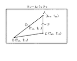
図8、図9は、かかるテクスチャデータの貼り付けを説明する図である。即ち、図8は、CRTディスプレー等の表示装置に表示するために、二次元座標平面に展開され、フレームバッファに格納されたポリゴンの一例である。
【0005】
図示されるかかるポリゴンPは、3頂点A、B、Cを有し、それぞれの頂点は貼り付けられるテクスチャデータを格納するテクスチャマップ上のX、Y2軸の座標を頂点データとして有する。
【0006】
例えば、頂点Aの画素に貼り付けられるテクスチャデータの格納位置として、図8に示されるように図9のテクスチャマップ上の座標データ(Tx0,Ty0)を有する。同様に、頂点Bは座標データ(Tx1,Ty1)を有し、頂点Cは座標データ(Tx2,Ty2)を有する。
【0007】
更に、例えば頂点Aと頂点Bの稜線上の点Dの画素に対しては、頂点Aの座標データ(Tx0,Ty0)と頂点Bの座標データ(Tx1,Ty1)を線型もしくはパースペクティブ補間をして、図9に示されるように、テクスチャマップ上の座標Dのデータ(Txi,Tyi)が求められる。
【0008】
ポリゴンPを構成する他の全ての画素に対しても、同様に線型もしくはパースペクティブ補間によりテクスチャマップ上の座標データが求められる。
【0009】
一方、テクスチャマップは、物体のテクスチャ種類毎に例えば、物体が岩であれば岩肌を表現するデータ、木材であれば木肌等を表現するデータがマップ状に展開され、メモリ装置に格納される。即ち、一つの岩における岩肌、一本の樹の木肌等は、1つのデータで定義できるようには均一ではなく、また連続性を持って変化する。
【0010】
従って、テクスチャマップは、岩肌、木肌等のテクスチャをX、Y2軸座標平面に展開したものであり、X、Y2軸座標位置を特定することにより、対応する特定位置の岩肌、木肌等のテクスチャが求められる。
【0011】
ここで、図10に示されるテクスチャマップの2軸平面とポリゴンの一画素との関係を考察する。図10において、太線で囲われた領域70は、ポリゴンを構成する1画素に対応してテクスチャマップの座標を指定した範囲である。領域71〜74は、テクスチャマップ上の複数の画素である。従って、この領域70に対し、テクスチャマップから読み出されるテクスチャデータに基づきテクスチャが該当の画素に貼り付けられる。
【0012】
しかし、上記のようにポリゴンを構成する1画素とテクスチャマップの画素とは必ずしも対応せず、ポリゴンを構成する1画素で指定される領域70は、テクスチャマップの隣接する複数の画素に跨る。図10の例では、領域70は、テクスチャマップの隣接する4つの画素71〜74に跨って重なる。
【0013】
このために、領域70に対応するポリゴンを構成する1画素に対するテクスチャは、隣接する4つの画素71〜74のデータを領域70の重なる面積に応じて混合して、対応するテクスチャデータを求めることが行われる。
【0014】
しかし、ポリゴンの中には、一部に穴の開いた部分を表現するものがある。この開いた部分に対応するテクスチャデータは透明色となる。従って、かかる場合は、ポリゴンに対しテクスチャを貼り付ける際に混合されるテクスチャマップ上の当該ポリゴンに対応する複数の画素の中に、透明であるテクスチャ画素が存在することになる。
【0015】
かかる場合は、混合に際し留意が必要である。なぜならば、透明色を隣接する画素に混合する場合は、色合いが異質になる恐れがあるからである。
【0016】
ここで上記したように、面積に応じて複数画素のテクスチャデータを混合する場合、図10でのテクスチャの画素71〜74の色をそれぞれ color0、 color1、 color2、 color3 とし、更に color1 が透明であるとする時、関係する面積に応じた寄与分から正規化した想定される計算式として数1または数2のように表わされる。
【0017】
【数1】

または、
【0019】
【数2】
color=color0(1-x)(1-y)+color1x(1-y)+color2(1-x)y+color3xy
即ち、数1では透明である color1 の画素72のデータを除外して計算する。一方、数2は、透明である color1 の画素72のデータも含めて計算している。
【0020】
【発明が解決しようとする課題】
上記数1、数2のいずれの計算方法においても問題がある。前者の場合は透明である画素の色は、無視することが出来る。しかし、除算を行うために回路構成が複雑となる。
【0021】
一方、後者の場合は、除算を行うための回路構成は必要でなくなるが、透明であるはずの画素72の色が混合されてしまう。この場合、透明な画素72にもテクスチャマップ上の隣接の画素の色と整合性を与える色を与えておくことが必要となり、データ処理上煩雑となる。
【0022】
したがって、本発明の目的は、かかる問題を解決するために、テクスチャマップ上の透明である画素の色を混合しない回路構成であって、構成が簡易な複数画素混合方法及び回路を提供することにある。
【0023】
更に本発明の目的は、上記の本発明に従う複数画素混合方法及び回路を用いた画像処理装置を提供することにある。
【0024】
【課題を解決するための手段】
上記の本発明の課題を達成する複数画素混合方法の第1の構成は、ポリゴンを構成する画素に対応するテクスチャマップ上の複数画素を混合して、該ポリゴンを構成する画素に貼り付けるテクスチャデータを求める複数画素混合方法において、該テクスチャマップ上の複数画素の中に透明画素があるか否かを判断し、透明画素がない場合は、該テクスチャマップ上の複数画素を該ポリゴンを構成する画素が対応する割合に応じて混合し、該テクスチャマップ上の複数画素の一部が透明画素である場合は、該透明画素を他の隣接する透明でない画素で置き換え、更に、該テクスチャマップ上の複数画素の全てが透明画素である場合は、該テクスチャマップ上の複数画素を無視するようにする。
【0025】
更に、本発明に従う複数画素混合方法の第2の構成は、ポリゴンを構成する画素に対応するテクスチャマップ上の複数画素を混合して、該ポリゴンを構成する画素に貼り付けるテクスチャデータを求める複数画素混合方法において、該テクスチャマップ上の一の行アドレス方向に隣接する第1の複数画素に透明画素があるか否かを判断し、該一の行アドレス方向に隣接する第1の複数画素に透明画素がない場合は、該第1の複数画素を該ポリゴンを構成する画素が対応する割合に応じて混合し、該一の行アドレス方向に隣接する第1の複数画素の一部の画素が透明画素である場合は、該透明画素を隣接する透明でない画素で置き換え、該一の行アドレス方向に隣接する第1の複数画素の全てが透明画素である場合は、該複数画素を無視する第1の工程と、
該テクスチャマップ上の該一の行に隣接する行アドレス方向に隣接する第2の複数画素に透明画素があるか否かを判断し、該一の行に隣接する行アドレス方向に隣接する第2の複数画素に透明画素がない場合は、該第2の複数画素を該ポリゴンを構成する画素が対応する割合に応じて混合し、該一の行に隣接する行アドレス方向に隣接する第2の複数画素の一部の画素が透明画素である場合は、該透明画素を隣接する透明でない画素で置き換え、該一の行に隣接する行アドレス方向に隣接する第2の複数画素の全てが透明画素である場合は、該第2の複数画素を無視する第2の工程と、
該第1の工程により得られる第1のテクスチャ画素データと該第2の工程により得られる第2のテクスチャ画素データを比較し、該第1、第2のテクスチャ画素データのいずれも透明でない場合は、該第1、第2のテクスチャ画素データを該ポリゴンを構成する画素が対応する割合に応じて混合し、該第1、第2のテクスチャ画素データのいずれかが透明である場合は、透明であるテクスチャ画素データを他方の透明でないテクスチャ画素データで置き換え、いずれも透明である場合は、該第1及び第2のテクスチャ画素データを無視する第3の工程を有する。
【0026】
また、本発明に従う複数画素混合回路の第1の構成は、ポリゴンを構成する画素に対応するテクスチャマップ上の複数画素を混合して、該ポリゴンを構成する画素に貼り付けるテクスチャデータを求める複数画素混合回路において、テクスチャマップ上の隣接する複数画素を、該ポリゴンを構成する画素が対応する割合に応じて混合する補間演算回路と、該補間演算回路の出力及び、該隣接する複数画素と、該複数画素のそれぞれが透明であるか否かを示すフラグを選択信号として入力し、該選択信号により、該複数画素のいずれもが透明でない場合は、該補間演算回路の出力を有効とし、該複数画素のいずれかが透明である場合は、該複数画素の透明で無い画素を有効とし、該複数画素のいずれもが透明である場合は、出力を無効とする選択回路を有して構成される。
【0027】
更にまた、本発明に従う複数画素混合回路の第2の構成は、第1の複数画素混合回路の構成において、更に、前記隣接する複数画素のアンド論理を出力するアンドゲートを有する。
【0028】
更に、本発明に従う複数画素混合回路の第3の構成は、第2の構成の複数画素混合回路を3組有し、第1及び第2の組の複数画素混合回路の出力を、第3の組の複数画素混合回路の前記補間演算回路の2つの入力とする。
【0029】
また、本発明に従う画像処理装置の第1の構成は、仮想3次元空間内に配置された物体を複数のポリゴンで構成して画像表示する画像処理装置において、X,Y2軸で特定される複数の座標位置にテクスチャデータを格納するテクスチャマップを格納するメモリ装置と、該複数のポリゴンのそれぞれを構成するピクセル毎に、該テクスチャマップから読み出したテクスチャデータを貼り付けるテクスチャ貼り付け回路を有し、該テクスチャ貼り付け回路は、テクスチャマップ上の隣接する複数画素を、該ポリゴンを構成する画素が対応する割合に応じて混合する補間演算回路と、該補間演算回路の出力及び、該隣接する複数画素と、該複数画素のそれぞれが透明であるか否かを示すフラグを選択信号として入力し、該選択信号により、該複数画素のいずれもが透明でない場合は、該補間演算回路の出力を有効とし、該複数画素のいずれかが透明である場合は、該複数画素の透明で無い画素を有効とし、該複数画素のいずれもが透明である場合は、出力を無効とする選択回路を備えた複数画素混合回路を含む。
【0030】
更に、本発明に従う画像処理装置の第2の構成は、第1の構成において、前記複数画素混合回路は、前記隣接する複数画素のアンド論理を出力するアンドゲートを有する。
【0031】
また、本発明に従う画像処理装置の第3の構成は、第1の構成において、前記複数画素混合回路を3組有し、第1及び第2の組の複数画素混合回路の出力を、第3の組の複数画素混合回路の前記補間演算回路の2つの入力とする。
【0032】
【発明の実施の形態】
以下本発明の実施の形態を図面に従い説明する。尚、図面において、同一または類似のものには、同一の参照番号または参照記号を付して説明する。
【0033】
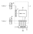
図1は、本発明の複数画素混合方法を用いた画像処理装置の構成ブロック図である。
【0034】
図1において、CPU1は、ポリゴンを使用した画像を処理するためのプログラムの実行を制御するものである。CPU1にはプログラムの進行に伴いディスプレー装置12上に表示するポリゴンの頂点データやレジスタセットファンクションを一次的に蓄えておくメモリであるデータバッファ2が接続されている。
【0035】
このデータバッファ2には、前記データに従って、3次元空間内にポリゴンを配置し、これをディスプレー装置12上に表示するために2次元座標系に変換するためのジオメトリ処理部3が接続されている。
【0036】
更に、表示する各ポリゴンに対し、着色、シェーディング、テクスチャの貼り付けを行うレンダリング処理部10が接続されている。レンダリング処理部10の出力側には、フレームバッファ11が接続され、表示される一画面分のデータが格納される。フレームバッファ11にCRT等のディスプレー装置12が接続され、フレームバッファ11の内容が順次表示される。
【0037】
ここで、上記ジオメトリ処理部3は、データバッファ2からプログラムの進行及び処理速度に対応して、ポリゴンの頂点データ(頂点座標、頂点カラー、テクスチャマップ座標、頂点透明度及び頂点の法線ベクトル等を有する)やレジスタセットファンクションを読み出す。
【0038】
ジオメトリ処理部3は、頂点座標データに基づき3次元空間にポリゴンを配置し、3次元空間のどの領域まで表示対象とするかのビューポートの決定、法線ベクトルに基づき各頂点の輝度の計算等を行う。また、ビューポートよりはみ出すポリゴンの頂点除去即ち、クリッピングを行う。更に、ビューポートに配置されたポリゴンを所定の視点を基準に2次平面に投影して3次元から2次元への座標変換を行う。
【0039】
2次元座標に座標変換されたポリゴンデータは、レンダリング処理部10に送られる。レンダリング処理部10は、塗り潰し回路4、テクスチャ貼り付け回路5、デプステスト回路7、ブレンディング回路9から構成されている。
【0040】
塗り潰し回路4は、ポリゴンの各頂点で囲まれた範囲にある画素(ピクセル)の情報を計算し、他のレンダリング処理部10内の各回路に渡す機能を有する。上記計算は、ポリゴンの各頂点間にあるピクセルの情報を対応の両頂点の情報を基に、例えば線型補間または、パースペクティブ補間等の補間を行うものである。先に図8において説明した頂点A,Bの頂点データからピクセルDのデータを求める如くである。
【0041】
テクスチャ貼り付け回路5は、ピクセルに対応したテクスチャをテクスチャマップ6から読み出し、ピクセルのカラーを計算して求める回路である。ピクセルのカラーを計算して求める回路の構成に本発明の複数画素混合方法及び回路の構成が適用されている。
【0042】
従って、かかる部分の方法及び回路構成については、本発明の実施例として後に詳細に説明する。
【0043】
デプステスト回路7は、複数のポリゴンの前後関係を比較して、最も手前に配置されたポリゴンのデータをデプスバッファ8に記憶させる回路である。即ち、デプスバッファ8には、先に描いた図形(ポリゴン)のピクセルのZ値が記憶されている。
【0044】
そして、画面上の先に描かれたポリゴンと重なる位置に、新しくポリゴンを表示する場合、新しいポリゴンを構成する各ピクセルのZ値と、デプスバッファ8から読み出される先に描かれたポリゴンのピクセルのZ値とを比較する。比較の結果、新しいポリゴンのピクセルが手前の場合は、デプスバッファ8に当該ピクセルのZ値が書き込まれる。
【0045】
ブレンディング回路9は、フレームバッファ11から読み込んだ、先に描かれているポリゴンのピクセルのカラー情報と、新しく処理するポリゴンのピクセルのカラー情報とを混合し、フレームバッファ11に書き込む。このフレームバッファ11の情報が1画面分ずつディスプレー装置12に送られ表示される。
【0046】
次に、上記のような構成の画像処理装置における本発明を適用した複数画素混合方法及び回路の実施例構成を説明する。
【0047】
先に説明したように、ポリゴンを構成する1画素のテクスチャデータを求める場合、当該1画素のテクスチャマップ上の座標データ位置において、画素は面積を持つので、テクスチャマップの隣接する複数の画素と重なる。従って、テクスチャマップの隣接する複数の画素データを組み合わせて、当該ポリゴンを構成する1画素に対するテクスチャデータを生成することが行われる。
【0048】
図2は、図1のテクスチャ貼り付け回路5に含まれる主機能回路としての画素混合回路50と、テクスチャマップ6の詳細を示すブロック図である。
【0049】
テクスチャマップ6は、テクスチャデータがポリゴン対応に展開格納されるメモリアレー60、行アドレスデコーダ61及び列アドレスデコーダ62を有する。更に、テクスチャ貼り付け回路5には、テクスチャマップ6の行アドレスデコーダ61及び列アドレスデコーダ62にそれぞれ行アドレス、列アドレスを送るアドレスバッファ63、64を有する。
【0050】
テクスチャ貼り付け回路5は、塗り潰し回路4から入力されるポリゴンの画素データからテクスチャマップ6の座標位置データを抜き出し、前記行アドレスデコーダ61及び列アドレスデコーダ62に送る。
【0051】
メモリアレー60は、テクスチャ貼り付け回路5から入力した4組の行アドレスと列アドレスにより対応する座標位置にある4画素71〜74のcolor0,color1,color2,color3 のデータを読み出し、複数画素混合回路50に入力する。
【0052】
更に、複数画素混合回路50には、テクスチャ貼り付け回路5において求めたポリゴンの画素を特定する座標とテクスチャマップ60の画素位置とのずれ(x及びy)の値が入力される。
【0053】
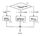
かかる複数画素混合回路50における動作フローが図3〜図5に示される。
【0054】
図10に示す例を用い、テクスチャメモリの画素71から74のテクスチャ(カラー:color0, color1, color2, color3)を混合し、ポリゴンの画素70に貼り付けるテクスチャデータ(カラー:color)を求める場合を考える。
【0055】
図3において、一の行アドレス方向の隣接画素のうち透明画素の有無を判断する(ステップS1)。この判断の結果、隣接画素のいずれも透明画素がない場合は、ポリゴンの画素の占める面積に応じた割合で混合する(ステップS2)。
【0056】
隣接画素のいずれかが、透明である場合は、他の画素で当該透明画素を置き換える(ステップS3)。更に、隣接画素のいずれも透明画素である場合は、画素テクスチャを無視する(ステップS4)。
【0057】
かかる処理を図10に当てはめると、一の行アドレス方向の隣接画素は画素71、72が対応し、画素72が透明であるので、ステップS3の処理が対応し、画素72の透明部分を不透明な画素71の画素で置き換える。即ち、画素71(color0)そのものが出力A(color01) となる。
【0058】
更に、図4において、一の行アドレスに隣接する行アドレス方向の隣接画素のうち透明画素の有無を判断する(ステップS5)。この判断結果による処理は、透明画素が無い場合は(ステップS6)の処理、一部の画素が透明である場合は(ステップS7)の処理、そして全てが透明画素である場合は(ステップS8)の処理となり、これらはそれぞれ図3の(ステップS2)、(ステップS3)、(ステップS4)に対応する。
【0059】
従って、図4の処理を図10に対応させると、隣接する行アドレス方向の隣接画素は画素73、74となる。そして、いずれの画素も透明では無いので画素73、74に対するポリゴンの画素70の占める割合に応じて混合され、出力B(color23) となる。
【0060】
更に、図5は、図3、図4の出力A,Bに基づく処理である。出力A,Bのうち透明画素の有無を判断する(ステップS9)。この判断結果による処理は、透明画素が無い場合は(ステップS10)の処理、一部の画素が透明である場合は(ステップS11)の処理、そして全てが透明画素である場合は(ステップS12)の処理となり、これらはそれぞれ図3、図4の(ステップS2、S6)、(ステップS3、S7)、(ステップS4、S8)に対応する。
【0061】
従って、図5の処理を図10に対応させると、出力A(color01) ,B(color23) のいずれも透明でないので、一の行アドレス方向の隣接画素71、72に対するポリゴンの画素70の占める大きさと、隣接する行アドレス方向の隣接画素73、74に対するポリゴンの画素70の占める大きさとの割合に応じて混合され、出力C(color) となる。
【0062】
図6は、かかる本発明の複数補画素混合方法を適用する複数画素混合回路50の実施例回路である。上記図3から図5の処理に対応して、3組の同様の回路で構成されている。補間演算回路501、選択回路502及びアンドゲート503により、図10に示す画素71と72を混合したデータ即ち、color0とcolor1を混合した出力color01 を得る。
【0063】
このために補間演算回路501、選択回路502及びアンドゲート503による第1の回路は、数3の計算を行う。
【0064】
【数3】
color01 = color0(1-x) + color1・x
同様に、補間演算回路504、選択回路505及びアンドゲート506による第2の回路は、数4の計算を行い、color2とcolor3を混合した出力color23 を得る。
【0065】
【数4】
color23 = color2(1-x) + color3・x
更に、補間演算回路507、選択回路508及びアンドゲート509による第3の回路は、数5の計算を行い、上記に求めたcolor02 とcolor23 を混合した最終出力としてcolor を得る。
【0066】
【数5】
color = color01(1-y) + color23・y
上記第1〜3の回路の計算原理は同様であるので、補間演算回路501、選択回路502及びアンドゲート503による第1の回路を代表例にして、回路の動作原理を説明する。
【0067】
上記第1の回路において、先ず補間演算回路501によりcolor0とcolor1の二つの画素71、72を混合する。補間演算回路501、504、507の構成例が図7に示される。
【0068】
図7において、入力信号の記号を一般化して示しているが、第1の回路に対応させると、dxi は、xであり、Datai,j 、 Datai,jは、それぞれ画素71、72のcolor0、 color1である。
【0069】
したがって、差回路151は、(1−x)を出力する。次いで、掛け算回路152、153からは、それぞれ(1−x)とcolor0の積color0・(1−x)、xとcolor1との積color1・xを出力する。
【0070】
和回路154は、掛け算回路152、153の出力の和を求め、color0・(1−x)+color1・xを出力し、選択回路502のA入力端に入力する。更に、選択回路502のB,C入力端にはそれぞれcolor0、color1が入力される。
【0071】
一方、それぞれのテクスチャマップの画素データには、画素が透明であるか否かの透明フラグ情報(画素が透明であれば、H論理を有する)が付加されている。従って、 選択回路502にはこのフラグ情報が端子S0 、S1 にセレクタ信号として入力される。
【0072】
選択回路502では、これら端子S0 、S1 に入力されるセレクタ信号の論理に基づき、補間演算回路501の混合出力color01 、または混合前の元の入力であるcolor0、color1が選択され、出力される。
【0073】
即ち、color0及びcolor1がともに透明でない(S0 =S1 =L論理)時、補間演算回路501の混合出力color01 が出力される。color0のみが透明である(S0 =H、S1 =L論理)時、color01 =color1として出力される。
【0074】
更に、color1のみが透明である(S0 =L、S1 =H論理)時、color01 =color0として出力される。color0、color1ともに透明である(S0 =H、S1 =H論理)時、混合の結果は特定されない。この時、選択回路502の出力color01 に対する透明フラグは、アンドゲート503の出力であり、H論理となる。この時、color01 の画素の色は無視される。
【0075】
上記の様にして、第1の回路により、数3の計算式に対応する出力color01 が得られる。更に、補間演算回路504、選択回路505及びアンドゲート506による第2の回路、補間演算回路507、選択回路508及びアンドゲート509による第3の回路の動作も第1の回路と同様である。
【0076】
即ち、第2の回路は、color2とcolor3を入力して、数4の計算に対応する出力color23 を出力する。第3の回路は、第1の回路の出力color01 と第2の回路の出力color23 を入力して数5の計算に対応する出力color を出力する。
【0077】
【発明の効果】
以上、図にしたがい実施例を説明したように、本発明に従う画素混合回路は、簡易な論理構成で実現でき且つ、透明な画素も考慮することが可能である。
【0078】
透明な画素の色は、隣接する他の色を適用することになるが、通常テクスチャマップにおいて、隣接する画素はある程度の相関を持った連続性があるために、画像品質に対し、影響を与えることがない。
【0079】
従って、本発明の適用により画像処理装置の低コスト化と、画像データの取り扱いを簡易にすることが可能である。
【図面の簡単な説明】
【図1】本発明の画素混合回路をテクスチャ貼り付け回路に用いた画像処理装置の構成ブロック図である。
【図2】本発明を適用したテクスチャ貼り付け回路とテクスチャマップメモリの関係を説明する図である。
【図3】複数画素混合回路50における動作のうち1の行の隣接画素の混合を説明するフロー図である。
【図4】複数画素混合回路50における動作のうち1の行に隣接する行の隣接画素の混合を説明するフロー図である。
【図5】複数画素混合回路50における動作のうち図3、図4のフローによる結果を混合を説明するフロー図である。
【図6】本発明の画素混合回路の一実施の形態の構成ブロック図である。
【図7】図3の実施の形態における相関演算回路の実施の形態の構成ブロック図である。
【図8】CRTディスプレー等の表示装置に表示するために、二次座標平面に展開され、フレームバッファに格納されたポリゴンの一例である。
【図9】ポリゴンの各ピクセルに対するテクスチャデータの貼り付けを説明する図である。
【図10】ポリゴンの各ピクセルを複数のテクスチャ画素データを組み合わせ求める計算を説明するための図である。
【符号の説明】
1 CPU
2 データバッファ
3 ジオメトリ処理部
4 塗り潰し回路
5 テクスチャ貼り付け回路
6 テクスチャマップ
7 デプステスト回路
8 デプスバッファ
9 ブレンディング回路
10 レンダリング処理部
11 フレームバッファ
12 ディスプレー装置
60 メモリセル
61 行アドレスデコード回路
62 列アドレスデコード回路
63、64 アドレスバッファ
50 画素混合回路
501、504、507 相関演算回路
502、505、508 選択回路
503、506、509 アンドゲート[0001]
BACKGROUND OF THE INVENTION
The present invention relates to a method for mixing a plurality of pixels on a texture map, a plurality of pixel mixing circuit and an image processing apparatus using the same.
[0002]
[Prior art]
2. Description of the Related Art In recent years, an image processing apparatus that displays an image of an object arranged in a virtual three-dimensional space using a plurality of polygons using computer graphic technology has become widespread. In addition, research and development are underway to make the displayed object more realistic.
[0003]
In such computer graphic technology, the details of the surface of the displayed object are called textures. By reading and pasting texture data from the texture map for each pixel (pixel) of the polygon that constitutes the corresponding polygon, color skin, texture, etc. are formed on the surface of the object.
[0004]
8 and 9 are diagrams for explaining pasting of such texture data. That is, FIG. 8 shows an example of a polygon developed on a two-dimensional coordinate plane and stored in a frame buffer for display on a display device such as a CRT display.
[0005]
The illustrated polygon P has three vertices A, B, and C, and each vertex has coordinates of X and Y axes on the texture map storing texture data to be pasted as vertex data.
[0006]
For example, as the storage location of texture data to be pasted to the pixels of the vertices A, with coordinates data (Tx0, Ty0) on the texture map of FIG. 9, as shown in FIG. Similarly, vertex B has coordinate data (Tx1, Ty1), and vertex C has coordinate data (Tx2, Ty2).
[0007]
Further, for example, for the pixel at the point D on the ridge line of the vertex A and the vertex B, the coordinate data (Tx0, Ty0) of the vertex A and the coordinate data (Tx1, Ty1) of the vertex B are linearly or perspectively interpolated. As shown in FIG. 9 , data (Txi, Tyi) of coordinates D on the texture map is obtained.
[0008]
Similarly, coordinate data on the texture map is obtained for all other pixels constituting the polygon P by linear or perspective interpolation.
[0009]
On the other hand, for each texture type of the object, for example, if the object is a rock, data representing the rock surface is developed, and if the object is wood, data representing a wood surface is developed in a map and stored in the memory device. That is, the rock surface of one rock, the bark of a tree, etc. are not uniform and can be changed with continuity so that they can be defined by one data.
[0010]
Therefore, the texture map is obtained by developing the texture of rock, wood, etc. on the X, Y2 axis coordinate plane, and by specifying the X, Y2 axis coordinate position, the texture of the rock, wood, etc. at the corresponding specific position can be obtained. Desired.
[0011]
Here, the relationship between the biaxial plane of the texture map shown in FIG. 10 and one pixel of the polygon will be considered. In FIG. 10, a
[0012]
However, as described above, one pixel constituting the polygon does not necessarily correspond to the pixel of the texture map, and the
[0013]
For this reason, the texture for one pixel constituting the polygon corresponding to the
[0014]
However, some polygons represent a part with a hole. The texture data corresponding to the opened portion is a transparent color. Therefore, in such a case, a transparent texture pixel exists among a plurality of pixels corresponding to the polygon on the texture map mixed when the texture is pasted on the polygon.
[0015]
In such a case, care must be taken during mixing. This is because when the transparent color is mixed into adjacent pixels, the hue may be different.
[0016]
As described above, when texture data of a plurality of pixels is mixed according to the area, the colors of the
[0017]
[Expression 1]
Or
[0019]
[Expression 2]
color = color0 (1-x) (1-y) + color1x (1-y) + color2 (1-x) y + color3xy
In other words, the calculation is performed by excluding the data of the
[0020]
[Problems to be solved by the invention]
There is a problem in either of the calculation methods of the
[0021]
On the other hand, in the latter case, a circuit configuration for performing division is not necessary, but the color of the
[0022]
Accordingly, an object of the present invention is to provide a multi-pixel mixing method and circuit having a simple circuit configuration that does not mix the color of transparent pixels on a texture map in order to solve such a problem. is there.
[0023]
A further object of the present invention is to provide an image processing apparatus using the plural pixel mixing method and circuit according to the present invention.
[0024]
[Means for Solving the Problems]
The first configuration of the multi-pixel mixing method that achieves the above-described problem of the present invention is that texture data that mixes a plurality of pixels on a texture map corresponding to pixels constituting a polygon and pastes them to the pixels constituting the polygon. In the multi-pixel mixing method for obtaining a pixel, it is determined whether or not there is a transparent pixel among the plurality of pixels on the texture map. If there is no transparent pixel, the plurality of pixels on the texture map are used as pixels constituting the polygon. Are mixed according to the corresponding ratio, and when some of the plurality of pixels on the texture map are transparent pixels, the transparent pixels are replaced with other adjacent non-transparent pixels, and further, the plurality of pixels on the texture map When all of the pixels are transparent pixels, a plurality of pixels on the texture map are ignored.
[0025]
Further, the second configuration of the multi-pixel mixing method according to the present invention is a multi-pixel which mixes a plurality of pixels on the texture map corresponding to the pixels constituting the polygon and obtains texture data to be pasted on the pixels constituting the polygon. In the mixing method, it is determined whether or not there is a transparent pixel in the first plurality of pixels adjacent to the one row address direction on the texture map, and the first plurality of pixels adjacent to the one row address direction is transparent. When there is no pixel, the first plurality of pixels are mixed according to the proportion corresponding to the pixels constituting the polygon, and some of the first plurality of pixels adjacent in the row address direction are transparent. If it is a pixel, the transparent pixel is replaced with an adjacent non-transparent pixel, and if all of the first plurality of pixels adjacent in the row address direction are transparent pixels, the plurality of pixels are ignored. And of the process,
It is determined whether there is a transparent pixel in the second plurality of pixels adjacent in the row address direction adjacent to the one row on the texture map, and the second adjacent in the row address direction adjacent to the one row In the case where there are no transparent pixels in the plurality of pixels, the second plurality of pixels are mixed according to the proportion corresponding to the pixels constituting the polygon, and the second pixel adjacent to the one row in the row address direction is mixed. When some of the plurality of pixels are transparent pixels, the transparent pixels are replaced with adjacent non-transparent pixels, and all of the second plurality of pixels adjacent in the row address direction adjacent to the one row are transparent pixels. A second step of ignoring the second plurality of pixels;
When the first texture pixel data obtained by the first step is compared with the second texture pixel data obtained by the second step, and neither of the first and second texture pixel data is transparent The first and second texture pixel data are mixed in accordance with the ratio of the pixels constituting the polygon, and if either of the first or second texture pixel data is transparent, If one texture pixel data is replaced with the other non-transparent texture pixel data and both are transparent, a third step of ignoring the first and second texture pixel data is included.
[0026]
Further, the first configuration of the multiple pixel mixing circuit according to the present invention is a multiple pixel for mixing texture pixels on a texture map corresponding to pixels constituting a polygon and obtaining texture data to be pasted on the pixels constituting the polygon. In the mixing circuit, an interpolating arithmetic circuit that mixes adjacent pixels on the texture map in accordance with a ratio corresponding to the pixels constituting the polygon, an output of the interpolating arithmetic circuit, and the adjacent plural pixels, A flag indicating whether or not each of the plurality of pixels is transparent is input as a selection signal. If none of the plurality of pixels is transparent according to the selection signal, the output of the interpolation operation circuit is validated, and the plurality of pixels When any of the pixels is transparent, the non-transparent pixel of the plurality of pixels is valid, and when any of the plurality of pixels is transparent, the output is invalidated. Configured with a circuit.
[0027]
Furthermore, the second configuration of the multiple pixel mixing circuit according to the present invention further includes an AND gate that outputs AND logic of the adjacent multiple pixels in the configuration of the first multiple pixel mixing circuit.
[0028]
Furthermore, the third configuration of the multi-pixel mixing circuit according to the present invention includes three sets of the multi-pixel mixing circuits of the second configuration, and outputs the outputs of the first and second sets of multi-pixel mixing circuits to the third configuration. Two inputs of the interpolation calculation circuit of the set of plural pixel mixing circuits are used.
[0029]
The first configuration of the image processing apparatus according to the present invention is an image processing apparatus that displays an image displayed by configuring an object arranged in a virtual three-dimensional space with a plurality of polygons. A memory device that stores a texture map that stores texture data at the coordinate position of the texture, and a texture pasting circuit that pastes the texture data read from the texture map for each pixel constituting each of the plurality of polygons, The texture pasting circuit includes an interpolation arithmetic circuit that mixes adjacent pixels on the texture map in accordance with a ratio corresponding to pixels constituting the polygon, an output of the interpolation arithmetic circuit, and the adjacent plural pixels. And a flag indicating whether or not each of the plurality of pixels is transparent is input as a selection signal, and the plurality of pixels are When none of the elements is transparent, the output of the interpolation operation circuit is valid, and when any of the plurality of pixels is transparent, the non-transparent pixel of the plurality of pixels is validated. In the case where the pixel is transparent, a multi-pixel mixing circuit including a selection circuit for invalidating the output is included.
[0030]
Furthermore, in a second configuration of the image processing apparatus according to the present invention, in the first configuration, the plural pixel mixing circuit has an AND gate that outputs an AND logic of the adjacent plural pixels.
[0031]
According to a third configuration of the image processing apparatus of the present invention, in the first configuration, there are three sets of the plurality of pixel mixing circuits, and the outputs of the first and second sets of the plurality of pixel mixing circuits are the third. Two inputs of the interpolation calculation circuit of the plurality of pixel mixing circuits in the set.
[0032]
DETAILED DESCRIPTION OF THE INVENTION
Embodiments of the present invention will be described below with reference to the drawings. In the drawings, the same or similar elements are denoted by the same reference numerals or reference symbols.
[0033]
FIG. 1 is a block diagram showing the configuration of an image processing apparatus using the multi-pixel mixing method of the present invention.
[0034]
In FIG. 1, a
[0035]
Connected to the
[0036]
Further, a
[0037]
Here, the
[0038]
The
[0039]
The polygon data coordinate-converted to two-dimensional coordinates is sent to the
[0040]
The filling
[0041]
The texture pasting circuit 5 is a circuit that reads a texture corresponding to a pixel from the
[0042]
Therefore, the method and circuit configuration of this part will be described in detail later as an embodiment of the present invention.
[0043]
The depth test circuit 7 is a circuit that compares the front-rear relations of a plurality of polygons and stores the data of the polygon arranged closest to the
[0044]
Then, when a new polygon is displayed at a position overlapping the previously drawn polygon on the screen, the Z value of each pixel constituting the new polygon and the pixel value of the previously drawn polygon read from the
[0045]
The
[0046]
Next, an example configuration of a multiple pixel mixing method and circuit to which the present invention is applied in the image processing apparatus having the above configuration will be described.
[0047]
As described above, when obtaining the texture data of one pixel constituting the polygon, the pixel has an area at the coordinate data position on the texture map of the one pixel, and thus overlaps a plurality of adjacent pixels of the texture map. . Accordingly, a plurality of adjacent pixel data in the texture map are combined to generate texture data for one pixel constituting the polygon.
[0048]
FIG. 2 is a block diagram showing details of the
[0049]
The
[0050]
The texture pasting circuit 5 extracts the coordinate position data of the
[0051]
The memory array 60 reads out the data of color0, color1, color2, color3 of the four
[0052]
Further, a shift (x and y) value between the coordinates specifying the polygon pixel obtained by the texture pasting circuit 5 and the pixel position of the texture map 60 is input to the plural
[0053]
The operation flow in the
[0054]
Using the example shown in FIG. 10, a case where textures (color: color0, color1, color2, color3) of
[0055]
In FIG. 3, it is determined whether or not there is a transparent pixel among adjacent pixels in one row address direction (step S1). If none of the adjacent pixels is a transparent pixel as a result of this determination, the pixels are mixed at a rate corresponding to the area occupied by the polygon pixel (step S2).
[0056]
If any of the adjacent pixels is transparent, the transparent pixel is replaced with another pixel (step S3). Further, if any of the adjacent pixels is a transparent pixel, the pixel texture is ignored (step S4).
[0057]
When this processing is applied to FIG. 10, the adjacent pixels in one row address direction correspond to the
[0058]
Further, in FIG. 4, it is determined whether or not there is a transparent pixel among adjacent pixels in the row address direction adjacent to one row address (step S5). The processing based on this determination result is the processing of (Step S6) when there are no transparent pixels, the processing of (Step S7) when some of the pixels are transparent, and the processing when all of the pixels are transparent (Step S8). These correspond to (Step S2), (Step S3), and (Step S4) in FIG. 3, respectively.
[0059]
Therefore, when the processing of FIG. 4 is made to correspond to FIG. 10, adjacent pixels in the row address direction become
[0060]
Further, FIG. 5 shows processing based on the outputs A and B of FIGS. It is determined whether or not there is a transparent pixel among the outputs A and B (step S9). The process based on the determination result is the process of (Step S10) when there are no transparent pixels, the process of (Step S11) when some of the pixels are transparent, and the process when all the pixels are transparent (Step S12). These correspond to (Steps S2, S6), (Steps S3, S7), and (Steps S4, S8) in FIGS. 3 and 4, respectively.
[0061]
Therefore, when the processing of FIG. 5 is made to correspond to FIG. 10, since the outputs A (color01) and B (color23) are not transparent, the size occupied by the
[0062]
FIG. 6 is an example circuit of a multiple
[0063]
For this purpose, the first circuit including the
[0064]
[Equation 3]
color01 = color0 (1-x) + color1 ・ x
Similarly, the second circuit including the
[0065]
[Expression 4]
color23 = color2 (1-x) + color3 ・ x
Further, the third circuit including the
[0066]
[Equation 5]
color = color01 (1-y) + color23 ・ y
Since the calculation principles of the first to third circuits are the same, the operation principle of the circuit will be described using the first circuit including the
[0067]
In the first circuit, first, the
[0068]
In FIG. 7, the symbol of the input signal is shown in a generalized manner. However, when it corresponds to the first circuit, dxi is x, and Datai, j and Datai, j are color0, color1.
[0069]
Therefore, the
[0070]
The
[0071]
On the other hand, transparency flag information indicating whether or not the pixel is transparent (having H logic if the pixel is transparent) is added to the pixel data of each texture map. Accordingly, the flag information is input to the
[0072]
In the
[0073]
That is, when both color0 and color1 are not transparent (S0 = S1 = L logic), the mixed output color01 of the
[0074]
Further, when only color1 is transparent (S0 = L, S1 = H logic), it is output as color01 = color0. When both color0 and color1 are transparent (S0 = H, S1 = H logic), the result of mixing is not specified. At this time, the transparent flag for the output color01 of the
[0075]
As described above, the output color01 corresponding to the equation (3) is obtained by the first circuit. Further, the operation of the second circuit by the
[0076]
That is, the second circuit inputs color2 and color3 and outputs an output color23 corresponding to the calculation of
[0077]
【The invention's effect】
As described above with reference to the drawings, the pixel mixing circuit according to the present invention can be realized with a simple logical configuration and can also consider transparent pixels.
[0078]
The color of a transparent pixel will apply other adjacent colors. However, in a texture map, the adjacent pixels have continuity with a certain degree of correlation, and this affects the image quality. There is nothing.
[0079]
Therefore, the application of the present invention can reduce the cost of the image processing apparatus and simplify the handling of the image data.
[Brief description of the drawings]
FIG. 1 is a configuration block diagram of an image processing apparatus using a pixel mixing circuit of the present invention for a texture pasting circuit.
FIG. 2 is a diagram for explaining the relationship between a texture pasting circuit to which the present invention is applied and a texture map memory;
FIG. 3 is a flowchart for explaining mixing of adjacent pixels in one row in the operation of the multiple
FIG. 4 is a flowchart for explaining mixing of adjacent pixels in a row adjacent to one row in the operation in the multiple
FIG. 5 is a flowchart for explaining the mixing of the results of the flows of FIGS. 3 and 4 among the operations in the multiple
FIG. 6 is a block diagram showing the configuration of an embodiment of a pixel mixing circuit according to the present invention.
7 is a block diagram showing the configuration of an embodiment of a correlation operation circuit in the embodiment of FIG. 3; FIG.
FIG. 8 is an example of a polygon developed on a secondary coordinate plane and stored in a frame buffer for display on a display device such as a CRT display.
FIG. 9 is a diagram for explaining pasting of texture data to each pixel of a polygon.
FIG. 10 is a diagram for explaining calculation for determining each pixel of a polygon by combining a plurality of texture pixel data.
[Explanation of symbols]
1 CPU
2
Claims (8)
該テクスチャマップ上の複数画素の中に透明画素があるか否かを判断し、
透明画素がない場合は、該テクスチャマップ上の複数画素を該ポリゴンを構成する画素が対応する割合に応じて混合し、
該テクスチャマップ上の複数画素の一部が透明画素である場合は、該透明画素を他の隣接する透明でない画素で置き換え、
更に、該テクスチャマップ上の複数画素の全てが透明画素である場合は、該テクスチャマップ上の複数画素を無視するようにしたことを特徴とするテクスチャマップ上の複数画素を混合する方法。In a multiple pixel mixing method for mixing texture pixels on a texture map corresponding to pixels constituting a polygon and obtaining texture data to be pasted on the pixels constituting the polygon,
Determining whether there are transparent pixels among the plurality of pixels on the texture map;
When there are no transparent pixels, a plurality of pixels on the texture map are mixed according to the ratio of the pixels constituting the polygon,
If some of the pixels on the texture map are transparent pixels, replace the transparent pixels with other adjacent non-transparent pixels;
Furthermore, when all of the plurality of pixels on the texture map are transparent pixels, the plurality of pixels on the texture map are ignored.
該テクスチャマップ上の一の行アドレス方向に隣接する第1の複数画素に透明画素があるか否かを判断し、該一の行アドレス方向に隣接する第1の複数画素に透明画素がない場合は、該第1の複数画素を該ポリゴンを構成する画素が対応する割合に応じて混合し、該一の行アドレス方向に隣接する第1の複数画素の一部の画素が透明画素である場合は、該透明画素を隣接する透明でない画素で置き換え、該一の行アドレス方向に隣接する第1の複数画素の全てが透明画素である場合は、該複数画素を無視する第1の工程と、
該テクスチャマップ上の該一の行に隣接する行アドレス方向に隣接する第2の複数画素に透明画素があるか否かを判断し、該一の行に隣接する行アドレス方向に隣接する第2の複数画素に透明画素がない場合は、該第2の複数画素を該ポリゴンを構成する画素が対応する割合に応じて混合し、該一の行に隣接する行アドレス方向に隣接する第2の複数画素の一部の画素が透明画素である場合は、該透明画素を隣接する透明でない画素で置き換え、該一の行に隣接する行アドレス方向に隣接する第2の複数画素の全てが透明画素である場合は、該第2の複数画素を無視する第2の工程と、
該第1の工程により得られる第1のテクスチャ画素データと該第2の工程により得られる第2のテクスチャ画素データを比較し、該第1、第2のテクスチャ画素データのいずれも透明でない場合は、該第1、第2のテクスチャ画素データを該ポリゴンを構成する画素が対応する割合に応じて混合し、該第1、第2のテクスチャ画素データのいずれかが透明である場合は、透明であるテクスチャ画素データを他方の透明でないテクスチャ画素データで置き換え、いずれも透明である場合は、該第1及び第2のテクスチャ画素データを無視する第3の工程を有することを特徴とするテクスチャマップ上の複数画素を混合する方法。In a multiple pixel mixing method for mixing texture pixels on a texture map corresponding to pixels constituting a polygon and obtaining texture data to be pasted on the pixels constituting the polygon,
When it is determined whether or not there is a transparent pixel in the first plurality of pixels adjacent in the one row address direction on the texture map, and there is no transparent pixel in the first plurality of pixels adjacent in the one row address direction In the case where the first plurality of pixels are mixed according to the proportion corresponding to the pixels constituting the polygon, and a part of the first plurality of pixels adjacent in the one row address direction is a transparent pixel Replacing the transparent pixel with an adjacent non-transparent pixel, and if all of the first plurality of pixels adjacent in the row address direction are transparent pixels, a first step of ignoring the plurality of pixels;
It is determined whether there is a transparent pixel in the second plurality of pixels adjacent in the row address direction adjacent to the one row on the texture map, and the second adjacent in the row address direction adjacent to the one row In the case where there are no transparent pixels in the plurality of pixels, the second plurality of pixels are mixed according to the proportion corresponding to the pixels constituting the polygon, and the second pixel adjacent to the one row in the row address direction is mixed. When some of the plurality of pixels are transparent pixels, the transparent pixels are replaced with adjacent non-transparent pixels, and all of the second plurality of pixels adjacent in the row address direction adjacent to the one row are transparent pixels. A second step of ignoring the second plurality of pixels;
When the first texture pixel data obtained by the first step is compared with the second texture pixel data obtained by the second step, and neither of the first and second texture pixel data is transparent The first and second texture pixel data are mixed in accordance with the ratio of the pixels constituting the polygon, and if either of the first or second texture pixel data is transparent, On a texture map characterized by having a third step of replacing one texture pixel data with the other non-transparent texture pixel data and ignoring the first and second texture pixel data if both are transparent A method of mixing a plurality of pixels.
テクスチャマップ上の隣接する複数画素を該ポリゴンを構成する画素が対応する割合に応じて混合する補間演算回路と、
該補間演算回路の出力及び、該隣接する複数画素と、該複数画素のそれぞれが透明であるか否かを示すフラグを選択信号として入力し、該選択信号により、該複数画素のいずれもが透明でない場合は、該補間演算回路の出力を有効とし、該複数画素のいずれかが透明である場合は、該複数画素の透明で無い画素を有効とし、該複数画素のいずれもが透明である場合は、出力を無効とする選択回路を
有して構成されることを特徴とする複数画素混合回路。In a multi-pixel mixing circuit that mixes a plurality of pixels on a texture map corresponding to pixels constituting a polygon and obtains texture data to be pasted on the pixels constituting the polygon.
An interpolation arithmetic circuit that mixes adjacent pixels on the texture map in accordance with a ratio of pixels corresponding to the polygon,
The output of the interpolation calculation circuit and the adjacent plural pixels and a flag indicating whether or not each of the plural pixels is transparent are input as selection signals, and all of the plural pixels are transparent by the selection signal. If not, the output of the interpolation operation circuit is enabled, and if any of the plurality of pixels is transparent, the non-transparent pixel of the plurality of pixels is enabled, and all of the plurality of pixels are transparent Comprises a selection circuit that disables the output, and is a multi-pixel mixing circuit.
更に、前記隣接する複数画素のアンド論理を出力するアンドゲートを有することを特徴とする複数画素混合回路。In claim 3,
The multi-pixel mixing circuit further comprising an AND gate that outputs an AND logic of the plurality of adjacent pixels.
X,Y2軸で特定される複数の座標位置にテクスチャデータを格納するテクスチャマップを格納するメモリ装置と、
該複数のポリゴンのそれぞれを構成するピクセル毎に、該テクスチャマップから読み出したテクスチャデータを貼り付けるテクスチャ貼り付け回路を有し、
該テクスチャ貼り付け回路は、テクスチャマップ上の隣接する複数画素を該ポリゴンを構成する画素が対応する割合に応じて混合する補間演算回路と、
該補間演算回路の出力及び、該隣接する複数画素と、該複数画素のそれぞれが透明であるか否かを示すフラグを選択信号として入力し、該選択信号により、該複数画素のいずれもが透明でない場合は、該補間演算回路の出力を有効とし、該複数画素のいずれかが透明である場合は、該複数画素の透明で無い画素を有効とし、該複数画素のいずれもが透明である場合は、出力を無効とする選択回路を
備えた複数画素混合回路を含むことを特徴とする画像処理装置。In an image processing apparatus that displays an image by configuring an object arranged in a virtual three-dimensional space with a plurality of polygons,
A memory device for storing a texture map for storing texture data at a plurality of coordinate positions specified by X and Y2 axes;
A texture pasting circuit for pasting texture data read from the texture map for each pixel constituting each of the plurality of polygons;
The texture pasting circuit mixes a plurality of adjacent pixels on the texture map in accordance with a ratio corresponding to pixels constituting the polygon;
The output of the interpolation calculation circuit and the adjacent plural pixels and a flag indicating whether or not each of the plural pixels is transparent are input as selection signals, and all of the plural pixels are transparent by the selection signal. If not, the output of the interpolation operation circuit is enabled, and if any of the plurality of pixels is transparent, the non-transparent pixel of the plurality of pixels is enabled, and all of the plurality of pixels are transparent Includes a multi-pixel mixing circuit including a selection circuit for invalidating the output.
更に、前記複数画素混合回路は、前記隣接する複数画素のアンド論理を出力するアンドゲートを有することを特徴とする画像処理装置。In claim 6,
The image processing apparatus further comprises an AND gate that outputs an AND logic of the adjacent pixels.
前記複数画素混合回路を3組有し、第1及び第2の組の複数画素混合回路の出力を、第3の組の複数画素混合回路の前記補間演算回路の2つの入力とすることを特徴とする画像処理装置。In claim 6,
Three sets of the plural pixel mixing circuits are provided, and outputs of the first and second sets of plural pixel mixing circuits are used as two inputs of the interpolation operation circuit of the third set of plural pixel mixing circuits. An image processing apparatus.
Priority Applications (2)
| Application Number | Priority Date | Filing Date | Title |
|---|---|---|---|
| JP33682396A JP3885262B2 (en) | 1996-12-17 | 1996-12-17 | Method for mixing a plurality of pixels on a texture map, and a plurality of pixel mixing circuit and image processing apparatus using the same |
| US08/986,192 US6005584A (en) | 1996-12-17 | 1997-12-05 | Method of blending a plurality of pixels on a texture map and a plural pixel blending circuit and image processing device using the same |
Applications Claiming Priority (1)
| Application Number | Priority Date | Filing Date | Title |
|---|---|---|---|
| JP33682396A JP3885262B2 (en) | 1996-12-17 | 1996-12-17 | Method for mixing a plurality of pixels on a texture map, and a plurality of pixel mixing circuit and image processing apparatus using the same |
Publications (2)
| Publication Number | Publication Date |
|---|---|
| JPH10177656A JPH10177656A (en) | 1998-06-30 |
| JP3885262B2 true JP3885262B2 (en) | 2007-02-21 |
Family
ID=18303012
Family Applications (1)
| Application Number | Title | Priority Date | Filing Date |
|---|---|---|---|
| JP33682396A Expired - Fee Related JP3885262B2 (en) | 1996-12-17 | 1996-12-17 | Method for mixing a plurality of pixels on a texture map, and a plurality of pixel mixing circuit and image processing apparatus using the same |
Country Status (2)
| Country | Link |
|---|---|
| US (1) | US6005584A (en) |
| JP (1) | JP3885262B2 (en) |
Families Citing this family (25)
| Publication number | Priority date | Publication date | Assignee | Title |
|---|---|---|---|---|
| US6078335A (en) * | 1998-06-01 | 2000-06-20 | Ati Technologies, Inc. | Method and apparatus for determining level of detail for texture filtering |
| US6297852B1 (en) * | 1998-12-30 | 2001-10-02 | Ati International Srl | Video display method and apparatus with synchronized video playback and weighted frame creation |
| US6181352B1 (en) | 1999-03-22 | 2001-01-30 | Nvidia Corporation | Graphics pipeline selectively providing multiple pixels or multiple textures |
| US6297833B1 (en) * | 1999-03-23 | 2001-10-02 | Nvidia Corporation | Bump mapping in a computer graphics pipeline |
| US6618048B1 (en) | 1999-10-28 | 2003-09-09 | Nintendo Co., Ltd. | 3D graphics rendering system for performing Z value clamping in near-Z range to maximize scene resolution of visually important Z components |
| US6717577B1 (en) | 1999-10-28 | 2004-04-06 | Nintendo Co., Ltd. | Vertex cache for 3D computer graphics |
| JP2001250115A (en) * | 2000-03-03 | 2001-09-14 | Sony Computer Entertainment Inc | Digital filter |
| US7119813B1 (en) * | 2000-06-02 | 2006-10-10 | Nintendo Co., Ltd. | Variable bit field encoding |
| US6636214B1 (en) | 2000-08-23 | 2003-10-21 | Nintendo Co., Ltd. | Method and apparatus for dynamically reconfiguring the order of hidden surface processing based on rendering mode |
| US7196710B1 (en) | 2000-08-23 | 2007-03-27 | Nintendo Co., Ltd. | Method and apparatus for buffering graphics data in a graphics system |
| US6707458B1 (en) | 2000-08-23 | 2004-03-16 | Nintendo Co., Ltd. | Method and apparatus for texture tiling in a graphics system |
| US7538772B1 (en) | 2000-08-23 | 2009-05-26 | Nintendo Co., Ltd. | Graphics processing system with enhanced memory controller |
| US6811489B1 (en) | 2000-08-23 | 2004-11-02 | Nintendo Co., Ltd. | Controller interface for a graphics system |
| US6700586B1 (en) | 2000-08-23 | 2004-03-02 | Nintendo Co., Ltd. | Low cost graphics with stitching processing hardware support for skeletal animation |
| US7576748B2 (en) | 2000-11-28 | 2009-08-18 | Nintendo Co. Ltd. | Graphics system with embedded frame butter having reconfigurable pixel formats |
| US6784895B1 (en) * | 2000-10-17 | 2004-08-31 | Micron Technology, Inc. | Programmable multiple texture combine circuit for a graphics processing system and method for use thereof |
| US7061507B1 (en) * | 2000-11-12 | 2006-06-13 | Bitboys, Inc. | Antialiasing method and apparatus for video applications |
| US6853373B2 (en) * | 2001-04-25 | 2005-02-08 | Raindrop Geomagic, Inc. | Methods, apparatus and computer program products for modeling three-dimensional colored objects |
| US20070109314A1 (en) * | 2003-05-23 | 2007-05-17 | Via Technologies, Inc. | Adaptive pixel-based blending method and system |
| US20050226087A1 (en) * | 2004-04-12 | 2005-10-13 | Kuo-Chang Wang | Protocol structure to accelerate memory transmission |
| US7573599B2 (en) * | 2004-05-20 | 2009-08-11 | Primax Electronics Ltd. | Method of printing geometric figures |
| US7852339B2 (en) * | 2006-10-23 | 2010-12-14 | Intel Corporation | Video composition optimization by the identification of transparent and opaque regions |
| JP4921113B2 (en) * | 2006-10-25 | 2012-04-25 | キヤノン株式会社 | Contact presentation apparatus and method |
| US7928992B2 (en) * | 2007-05-30 | 2011-04-19 | Kabushiki Kaisha Toshiba | System and method for transparent object rendering |
| CN103493105B (en) * | 2011-04-25 | 2017-04-05 | 林光雄 | Omnidirectional images edit routine and omnidirectional images editing device |
Family Cites Families (5)
| Publication number | Priority date | Publication date | Assignee | Title |
|---|---|---|---|---|
| US5889526A (en) * | 1994-11-25 | 1999-03-30 | Matsushita Electric Industrial Co., Ltd. | Interpolation apparatus and method, and image generation apparatus including such an apparatus |
| US5892516A (en) * | 1996-03-29 | 1999-04-06 | Alliance Semiconductor Corporation | Perspective texture mapping circuit having pixel color interpolation mode and method thereof |
| US5903270A (en) * | 1997-04-15 | 1999-05-11 | Modacad, Inc. | Method and apparatus for mapping a two-dimensional texture onto a three-dimensional surface |
| US5781197A (en) * | 1996-07-26 | 1998-07-14 | Hewlett-Packard Company | Method for maintaining contiguous texture memory for cache coherency |
| US5900882A (en) * | 1996-11-15 | 1999-05-04 | Samsung Electronics Co., Ltd. | Determining texture coordinates in computer graphics |
-
1996
- 1996-12-17 JP JP33682396A patent/JP3885262B2/en not_active Expired - Fee Related
-
1997
- 1997-12-05 US US08/986,192 patent/US6005584A/en not_active Expired - Fee Related
Also Published As
| Publication number | Publication date |
|---|---|
| US6005584A (en) | 1999-12-21 |
| JPH10177656A (en) | 1998-06-30 |
Similar Documents
| Publication | Publication Date | Title |
|---|---|---|
| JP3885262B2 (en) | Method for mixing a plurality of pixels on a texture map, and a plurality of pixel mixing circuit and image processing apparatus using the same | |
| US5877769A (en) | Image processing apparatus and method | |
| JP3203160B2 (en) | Volume rendering apparatus and method | |
| US6172687B1 (en) | Memory device and video image processing apparatus using the same | |
| JP2002304636A (en) | Method and device for image generation, recording medium with recorded image processing program, and image processing program | |
| JPH05307610A (en) | Texture mapping method and its device | |
| WO2000002165A1 (en) | Method for generating polygon data and image display using the same | |
| JPH0771936A (en) | Device and method for processing image | |
| JP2612221B2 (en) | Apparatus and method for generating graphic image | |
| JPS6380375A (en) | Texture mapping device | |
| KR100277803B1 (en) | 3D graphic display | |
| JPH11259671A (en) | Image displaying method and image display device executing the same | |
| JP3649478B2 (en) | Image information processing apparatus and image information processing method | |
| US6373494B1 (en) | Signal processing apparatus and image processing apparatus | |
| JPH09245191A (en) | Transparency transformation method, its device and image processor | |
| WO2023173728A1 (en) | Graphic rendering method and apparatus, and storage medium | |
| JP3052839B2 (en) | Image processing apparatus and processing method thereof | |
| US20030169272A1 (en) | Image generation apparatus and method thereof | |
| US20050275733A1 (en) | Method and apparatus of rendering a video image by polynomial evaluation | |
| JPH06266852A (en) | Picture synthesizing device | |
| US6476818B1 (en) | Storage circuit control device and graphic computation device | |
| JP4622165B2 (en) | Image memory control device, graphic operation device, and rendering processing method | |
| JPH11185052A (en) | Device and method for calculating texture mapping coordinate of three-dimensional computer graphics | |
| JP2001134777A (en) | Three-dimensional graphics system, arithmetic processor and recording medium | |
| JP4042204B2 (en) | Graphic operation apparatus and method |
Legal Events
| Date | Code | Title | Description |
|---|---|---|---|
| A521 | Written amendment |
Free format text: JAPANESE INTERMEDIATE CODE: A523 Effective date: 20031209 |
|
| A621 | Written request for application examination |
Free format text: JAPANESE INTERMEDIATE CODE: A621 Effective date: 20031209 |
|
| TRDD | Decision of grant or rejection written | ||
| A01 | Written decision to grant a patent or to grant a registration (utility model) |
Free format text: JAPANESE INTERMEDIATE CODE: A01 Effective date: 20061031 |
|
| A61 | First payment of annual fees (during grant procedure) |
Free format text: JAPANESE INTERMEDIATE CODE: A61 Effective date: 20061113 |
|
| R150 | Certificate of patent or registration of utility model |
Free format text: JAPANESE INTERMEDIATE CODE: R150 |
|
| LAPS | Cancellation because of no payment of annual fees |