JP3881092B2 - LCD panel - Google Patents
LCD panel Download PDFInfo
- Publication number
- JP3881092B2 JP3881092B2 JP24527897A JP24527897A JP3881092B2 JP 3881092 B2 JP3881092 B2 JP 3881092B2 JP 24527897 A JP24527897 A JP 24527897A JP 24527897 A JP24527897 A JP 24527897A JP 3881092 B2 JP3881092 B2 JP 3881092B2
- Authority
- JP
- Japan
- Prior art keywords
- liquid crystal
- substrate
- display panel
- light
- crystal display
- Prior art date
- Legal status (The legal status is an assumption and is not a legal conclusion. Google has not performed a legal analysis and makes no representation as to the accuracy of the status listed.)
- Expired - Fee Related
Links
Images


Classifications
-
- G—PHYSICS
- G02—OPTICS
- G02F—OPTICAL DEVICES OR ARRANGEMENTS FOR THE CONTROL OF LIGHT BY MODIFICATION OF THE OPTICAL PROPERTIES OF THE MEDIA OF THE ELEMENTS INVOLVED THEREIN; NON-LINEAR OPTICS; FREQUENCY-CHANGING OF LIGHT; OPTICAL LOGIC ELEMENTS; OPTICAL ANALOGUE/DIGITAL CONVERTERS
- G02F1/00—Devices or arrangements for the control of the intensity, colour, phase, polarisation or direction of light arriving from an independent light source, e.g. switching, gating or modulating; Non-linear optics
- G02F1/01—Devices or arrangements for the control of the intensity, colour, phase, polarisation or direction of light arriving from an independent light source, e.g. switching, gating or modulating; Non-linear optics for the control of the intensity, phase, polarisation or colour
- G02F1/13—Devices or arrangements for the control of the intensity, colour, phase, polarisation or direction of light arriving from an independent light source, e.g. switching, gating or modulating; Non-linear optics for the control of the intensity, phase, polarisation or colour based on liquid crystals, e.g. single liquid crystal display cells
- G02F1/133—Constructional arrangements; Operation of liquid crystal cells; Circuit arrangements
- G02F1/1333—Constructional arrangements; Manufacturing methods
- G02F1/1335—Structural association of cells with optical devices, e.g. polarisers or reflectors
- G02F1/133553—Reflecting elements
- G02F1/133555—Transflectors
-
- G—PHYSICS
- G02—OPTICS
- G02F—OPTICAL DEVICES OR ARRANGEMENTS FOR THE CONTROL OF LIGHT BY MODIFICATION OF THE OPTICAL PROPERTIES OF THE MEDIA OF THE ELEMENTS INVOLVED THEREIN; NON-LINEAR OPTICS; FREQUENCY-CHANGING OF LIGHT; OPTICAL LOGIC ELEMENTS; OPTICAL ANALOGUE/DIGITAL CONVERTERS
- G02F1/00—Devices or arrangements for the control of the intensity, colour, phase, polarisation or direction of light arriving from an independent light source, e.g. switching, gating or modulating; Non-linear optics
- G02F1/01—Devices or arrangements for the control of the intensity, colour, phase, polarisation or direction of light arriving from an independent light source, e.g. switching, gating or modulating; Non-linear optics for the control of the intensity, phase, polarisation or colour
- G02F1/13—Devices or arrangements for the control of the intensity, colour, phase, polarisation or direction of light arriving from an independent light source, e.g. switching, gating or modulating; Non-linear optics for the control of the intensity, phase, polarisation or colour based on liquid crystals, e.g. single liquid crystal display cells
- G02F1/133—Constructional arrangements; Operation of liquid crystal cells; Circuit arrangements
- G02F1/1333—Constructional arrangements; Manufacturing methods
- G02F1/1335—Structural association of cells with optical devices, e.g. polarisers or reflectors
- G02F1/133509—Filters, e.g. light shielding masks
- G02F1/133514—Colour filters
-
- G—PHYSICS
- G02—OPTICS
- G02F—OPTICAL DEVICES OR ARRANGEMENTS FOR THE CONTROL OF LIGHT BY MODIFICATION OF THE OPTICAL PROPERTIES OF THE MEDIA OF THE ELEMENTS INVOLVED THEREIN; NON-LINEAR OPTICS; FREQUENCY-CHANGING OF LIGHT; OPTICAL LOGIC ELEMENTS; OPTICAL ANALOGUE/DIGITAL CONVERTERS
- G02F1/00—Devices or arrangements for the control of the intensity, colour, phase, polarisation or direction of light arriving from an independent light source, e.g. switching, gating or modulating; Non-linear optics
- G02F1/01—Devices or arrangements for the control of the intensity, colour, phase, polarisation or direction of light arriving from an independent light source, e.g. switching, gating or modulating; Non-linear optics for the control of the intensity, phase, polarisation or colour
- G02F1/13—Devices or arrangements for the control of the intensity, colour, phase, polarisation or direction of light arriving from an independent light source, e.g. switching, gating or modulating; Non-linear optics for the control of the intensity, phase, polarisation or colour based on liquid crystals, e.g. single liquid crystal display cells
- G02F1/133—Constructional arrangements; Operation of liquid crystal cells; Circuit arrangements
- G02F1/1333—Constructional arrangements; Manufacturing methods
- G02F1/1334—Constructional arrangements; Manufacturing methods based on polymer dispersed liquid crystals, e.g. microencapsulated liquid crystals
Description
【0001】
【発明の属する技術分野】
本発明は液晶表示パネルの構造に関し、とくに第1の基板上に設ける対向電極と第2の基板上に設ける信号電極と第1の基板と第2の基板との間に封入する液晶とを備え、対向電極と信号電極との交点に複数の画素部を有し、各画素部に電圧を印加し液晶の光学特性変化を利用し表示を行う液晶表示パネル、または第1の基板上に設ける第1の電極と第2の電極と、第1の電極と第2の電極との重なり合う領域に設ける非線形抵抗素子を有し、非線形抵抗素子は対向電極と表示電極に接続し、第1の基板に対向する第2の基板上に設ける信号電極と、第1の基板と第2の基板との間に封入する液晶とを備え、表示電極と信号電極との交点に複数の画素部を有し、非線形抵抗素子を介して各画素部に電圧を印加し液晶の光学特性変化を利用し表示を行う液晶表示パネルに関するものである。
さらに、第1の基板、または第2の基板上にカラーフィルター、または反射膜からなる光透過減衰膜を有する、カラー液晶表示パネル、または反射型液晶表示パネルに関するものである。
さらに、液晶とポリマーを有する液晶層を利用する液晶表示パネルに関するものである。
さらに、時計装置に利用する液晶表示パネルに関するものである。
【0002】
【従来の技術】
近年、液晶パネルを用いた液晶表示パネルの表示容量は、大容量化の一途をたどっている。
そして、第1の基板上に設ける対向電極と第2の基板上に設ける信号電極と第1の基板と第2の基板との間に封入する液晶とを備え、対向電極と信号電極との交点に複数の画素部を有し、各画素部に電圧を印加し液晶の光学特性変化を利用し表示を行う単純マトリクス構成の液晶表示パネルにマルチプレクス駆動を用いる手段がある。
【0003】
さらに、各画素部に非線形抵抗素子を設けるアクティブマトリクス手段の液晶表示パネルが採用されている。
非線形抵抗素子には、大別すると薄膜トランジスタを用いる三端子系と、非線系抵抗素子を用いる二端子系とがある。
この二端子系には、ダイオード型や、バリスタ型や、TFD型などが開発されている。
【0004】
さらに、他の表示装置に比較し液晶の利点である低消費電力化のために、より明るい表示装置が要求されている。そのためには、各画素部の透過率を向上すること。または画素部と各画素部の間隙との比率である、いわゆる開口率を向上する手段がある。
さらに、カラー化のために液晶の屈折率の差を利用する方法も行われているが液晶表示パネルと観察者の位置関係または画素部の位置と観察者の位置関係により色合いが変化してしまうことがおこる。
さらに、カラーフィルターを画素部の全域に形成する方法が利用されているが暗くなるため、明るさが重要な液晶表示パネルには適さない。
さらに、反射膜を画素部の全面に形成する場合には、反射膜を透過して表示を行うための補助光源の光を遮蔽してしまう。
【0005】
さらに、画素部の集合体からなる画素部と画素部の周囲に設ける見切り部とでは、目的が異なるため、カラーフィルターまたは反射膜を制御する必要がある。
また、液晶にポリマーを含む液晶層の場合には、液晶層への紫外線の照射が必要となるが、カラーフィルターと反射膜により紫外線が遮断され、液晶層へ紫外線を充分に照射することができない。
【0006】
さらに、液晶とポリマーを含む液晶層へ色素を含む場合には、さらに紫外線の照射が難しくなる。
【0007】
以下、従来技術を2端子系の非線形抵抗素子を用いる場合に関して図29と図30とを用いて説明する。図29はカラーフィルターと反射膜とを画素部の全域に形成する液晶表示パネルの構成を示す平面図である。さらに図30は、図29の平面図におけるA−A線での断面を示す断面図である。以下図29と図30とを交互に用いて従来技術を説明する。
【0008】
第1の基板1の上には、タンタル(Ta)膜からなる第1の電極2と対向電極9を設け、この第1の電極2上に第1の電極2の陽極酸化膜である酸化タンタル(Ta2 O5 )からなる非線形抵抗層3を設ける。
さらにクロム(Cr)膜からなる第2の電極4を非線形抵抗層3上にオーバーラップするように設けて、非線形抵抗素子10を設ける。なお、この第2の電極4の一部領域は、アルミニウム(Al)からなる反射膜の表示電極5と接続している。
【0009】
一方、第2の基板6には、第1の基板1に形成するそれぞれの表示電極5の隙間からの光の漏れを防止するために酸化クロム膜(CrO)とクロム膜(Cr)の2層からなるブラックマトリクス7を設ける。
【0010】
さらに、第2の基板6上にはブラックマトリクス7の一部と重なり、表示電極55と対向する領域にカラーフィルター11、12、13を設ける。このカラーフィルター11、12、13は、青色と赤色と緑色との3色からなる。
さらに、カラーフィルター11、12、13は、表示電極5の領域ではとくに分割してなく、そしてカラーフィルター11、12、13間には光の透過する領域は設けていない。
【0011】
さらに、第2の基板6には、表示電極5と対向するように透明導電性膜である酸化インジウムスズ(ITO)からなる対向電極9を設ける。この対向電極9とカラーフィルター11、12、13との間には絶縁性保護膜8を設ける。
さらに、対向電極9に、外部回路の信号を印加するため、対向電極9はデーター電極(図示せず)が接続している。
【0012】
さらに、第1の基板1上に設ける第1の電極2は、非線形抵抗素子10を設けるために張り出している領域を設ける。そして、この張り出し領域が第2の電極4とオーバーラップして非線形抵抗素子10を構成している。
さらにまた図29の平面図に示すように、第1の電極2と表示電極5との間には、所定寸法の間隙を有している。
【0013】
表示電極5は、液晶16を介して対向電極9と重なり合うように配置することにより、液晶表示パネルの表示画素部19となる。
対向電極9とデーター電極に外部回路より駆動波形を印加し、非線形抵抗素子10を介して、表示電極5と対向電極9との間の領域の液晶の透過率変化によって、液晶表示パネルは所定の画像表示を行う。
【0014】
さらに第1の基板1と第2の基板6とは、液晶16の分子を規則的に並べるための処理層として、それぞれ配向膜21、21を設ける。
【0015】
さらにスペーサー17によって、第1の基板1と第2の基板6とを所定の間隙寸法をもって対向させ、第1の基板1と第2の基板6との間には、液晶層16を封入する。
液晶層16には、液晶とポリマーを混合するものを利用する。液晶層16は、第1の基板1または第2の基板6の面より紫外線を照射し、ポリマーを架橋反応する必要がある。しかし、第1の基板1上には、反射膜(光透過減衰膜)を有するため、紫外線を照射することはできない。さらに、第2の基板6上には、カラーフィルターを有するため、紫外線(波長300nmから400nm)は、カラーフィルターにより吸収され、液晶層16へ紫外線を効率よく照射することができない。
【0016】
さらに、第2の基板6側に外部光源28を設ける。液晶表示パネルは自己発光しないため、外部の光源が必要となる。この外部光源28を利用し液晶の光学特性変化を利用し、表示を行う。
【0017】
図29と図30に示す従来技術における液晶表示パネルは、表示画素部19の領域のカラーフィルター11、12、13は、1個の島状の構造をしている。
そのため、たとえば1表示画素部19領域の赤のカラーフィルター11には、とくに大きな光を透過できる領域はない。
【0018】
さらに、カラーフィルター11、12、13は、表示画素部19の周囲部に設けるブラックマトリクス7と一部で重なるため光が透過せず、色純度の良好な表示は可能であるが、暗い液晶表示パネルとなる。
またさらに、第1の基板1の反射膜を形成する面と逆の面(裏面)側に補助光源20を配置し、外部光源28が弱い場合には、液晶表示パネルの表示が見えないため、補助光源の光を利用する必要があるが、反射膜により光が遮蔽されるため、反射膜の裏面へ補助光源を配置することができなくなる。
【0019】
【発明が解決しようとする課題】
以上に説明したように、従来のカラーフィルター、または反射膜からなる光透過減衰膜を用いると、光源部の光が弱いときには、表示が暗くなりほとんど表示内容の認識できなくなる。また、カラーフィルターと反射膜を両方異なる基板上の用いる場合には、補助光源の利用を著しく制限する。
【0020】
さらに、反射型液晶表示パネルのときには外部光源を利用し、液晶表示パネルの光学変化に応じて表示をおこなうため、さらに明るさが重要となるため、光の有効利用が重要となる。
【0021】
さらに、非線形抵抗素子を有するアクティブマトリクス型液晶表示パネルのときには、対向電極と信号電極の交差領域の画素部からなる単純マトリクス型液晶表示パネルに比較し非線形抵抗素子を形成する領域が光を遮蔽するためさらに明るさが低下してしまう。
【0022】
また、液晶層への紫外線照射が必要な液晶とポリマーの混合液晶からなる高分子散乱型液晶を利用する場合には、異なる基板上にカラーフィルターと反射膜を形成すると液晶層への紫外線の照射を阻害する。
また、高分子散乱型液晶に色素を混合する場合には、高分子散乱型液晶へ紫外線を照射することが非常に難しくなる。
【0023】
〔発明の目的〕
本発明の目的は、上記課題を解決して、カラーフィルター、反射膜を有する液晶表示パネルにおいても透過率の向上をおこない、明るい表示性能を有する液晶表示パネルを提供するとともに、液晶層への光の照射を可能とする構造を提供することにある。
また、時計装置に利用するために、第1の基板と第2の基板に貫通孔を設ける場合に、貫通孔の影響を実際に利用する表示画素部に及ぶことを防止する必要がある。
【0024】
【課題を解決するための手段】
上記目的を達成するために、本発明の液晶表示パネルにおいては、下記記載の構成を採用する。
【0026】
本発明の液晶表示パネルは、第1の基板と第2の基板とのそれぞれに電極を設け、第1の基板と第2の基板との間に封入する液晶層とを備え、それぞれの電極の交点に画素部を有し、この画素部には反射膜とカラーフィルターとを備え、反射膜は、画素部内において開口部が設けられ、カラーフィルターは、画素部内においてカラーフィルターの周囲が、カラーフィルターの透過率より高くなるように、画素部より小さく、かつ反射膜の開口部より大きい島状に形成され、反射膜の開口部と重なる位置に島状のカラーフィルターを配置する。
【0027】
本発明の液晶表示パネルは、第1の基板上に設ける対向電極と、第2の基板上に設ける信号電極と、第1の基板と第2の基板との間に封入する液晶とを備え、対向電極と信号電極との交点に複数の画素部を有し、各画素部に電圧を印加し液晶の光学特性変化を利用し表示を行う液晶表示パネルの各画素部には、カラーフィルター、または反射膜の少なくとも一方からなる光透過減衰膜を有し、さらに各画素部には、複数の島状の光透過減衰膜を有し、複数の島状の光透過減衰膜の周囲には光の透過する開口部を有する。
【0028】
本発明の液晶表示パネルは、第1の基板上に設ける対向電極と、第2の基板上に設ける信号電極と、第1の基板と第2の基板との間に封入する液晶とを備え、対向電極と信号電極との交点に複数の画素部を有し、各画素部に電圧を印加し液晶の光学特性変化を利用し表示を行う液晶表示パネルの各画素部と、画素部の集合体からなる表示部の周囲に設ける見切り部とには、カラーフィルター、または反射膜の少なくとも一方からなる光透過減衰膜を有し、さらに各画素部には、複数の島状の光透過減衰膜を有し、複数の島状の光透過減衰膜の周囲には光の透過する開口部を有し、さらに、見切り部にも、複数の島状の光透過減衰膜を有し、複数の島状の光透過減衰膜の周囲には光の透過する開口部を有する。
【0029】
本発明の液晶表示パネルは、第1の基板上に設ける対向電極と、第2の基板上に設ける信号電極と、第1の基板と第2の基板との間に封入する液晶とを備え、対向電極と信号電極との交点に複数の画素部を有し、各画素部に電圧を印加し液晶の光学特性変化を利用し表示を行う液晶表示パネルの各画素部と、画素部の集合体からなる表示部の周囲に設ける見切り部とには、カラーフィルター、または反射膜の少なくとも一方からなる光透過減衰膜を有し、さらに、各画素部には、複数の島状の光透過減衰膜を有し、複数の島状の光透過減衰膜の周囲には光の透過する開口部を有し、さらに見切り部にも、複数の島状の光透過減衰膜を有し、複数の島状の光透過減衰膜の周囲には光の透過する開口部を有し、各画素部と見切り部に設ける開口部の密度が異なる。
【0030】
本発明の液晶表示パネルは、第1の基板上に設ける対向電極と、第2の基板上に設ける信号電極と、第1の基板と第2の基板との間に封入する液晶とを備え、対向電極と信号電極との交点に複数の画素部を有し、各画素部に電圧を印加し液晶の光学特性変化を利用し表示を行う液晶表示パネルの各画素部には、カラーフィルターと反射膜からなる光透過減衰膜を有し、さらに、各画素部の2種類の光透過減衰膜には、光の透過する開口部を有する。
【0031】
本発明の液晶表示パネルは、第1の基板上に設ける対向電極と、第2の基板上に設ける信号電極と、第1の基板と第2の基板との間に封入する液晶とを備え、対向電極と信号電極との交点に複数の画素部を有し、各画素部に電圧を印加し液晶の光学特性変化を利用し表示を行う液晶表示パネルの各画素部には、第1の基板上に反射膜からなる光透過減衰膜を有し、第2の基板上にカラーフィルターからなる光透過減衰膜を有し、さらに、各画素部の2種類の光透過減衰膜には、光の透過する開口部を有する。
【0032】
本発明の液晶表示パネルは、第1の基板上に設ける対向電極と、第2の基板上に設ける信号電極と、第1の基板と第2の基板との間に封入する液晶とを備え、対向電極と信号電極との交点に複数の画素部を有し、各画素部に電圧を印加し液晶の光学特性変化を利用し表示を行う液晶表示パネルの各画素部には、第1の基板上に反射膜からなる光透過減衰膜を有し、第2の基板上にカラーフィルターからなる光透過減衰膜を有し、さらに、各画素部の2種類の光透過減衰膜には、光の透過する開口部を有し、反射膜の設ける開口部とカラーフィルターカラーフィルターに設ける開口部とが各画素部において異なる位置に分布している。
【0033】
本発明の液晶表示パネルは、島状のカラーフィルター、または反射膜上の少なくとも一方の配向膜と開口部上の配向膜とは異なる配向特性を有する。
【0034】
本発明の液晶表示パネルは、第1の基板と第2の基板との間に封入する液晶層は、モノマーを紫外線にて架橋構造とするポリマーと液晶との混合物である。
【0035】
本発明の液晶表示パネルは、第1の基板と第2の基板との間に封入する液晶層は、モノマーを紫外線にて架橋構造とするポリマーと液晶との混合物であり、液晶層には、色素を有する。
【0036】
本発明の液晶表示パネルは、第1の基板と第2の基板との間に封入する液晶層は、モノマーを紫外線にて架橋構造とするポリマーと液晶との混合物であり、カラーフィルター、または配向膜の開口部を中心に架橋構造が進行している。
【0037】
本発明の液晶表示パネルは、第1の基板と第2の基板には、貫通孔を有し、貫通孔のごく近傍では、部分では、光透過減衰膜に開口部を有し、その周囲には、開口部を設けていない。
【0038】
[作用]
本発明の液晶表示パネルの各画素部に設けるカラーフィルター、または反射膜からなる光透過減衰膜には、光の透過する開口部を有する構造または複数の島状のカラーフィルター、または反射膜を有し、複数の島状のカラーフィルター、または反射膜の周囲には、光の透過する領域を有する構成を採用する。
そのため、カラーフィルターによる光の吸収、または反射膜による光の遮蔽があるが、光透過減衰膜の周囲に開口部を設けるため、光透過減衰膜の周囲では透過率が大きく、明るい表示が可能となる。
【0039】
さらに、各画素部に設けるカラーフィルターと反射膜の開口部の位置を異なる位置に分布することにより、カラーフィルターに設ける開口部の透過率の大きな領域では、カラーフィルター側より大きな光を透過することが可能となる。
また、反射膜に設ける開口部により、カラーフィルターの開口部とは異なる位置で透過率を大きくすることができるため、カラーフィルター側より光が入射する場合に場合には、カラーフィルターの開口部と反射膜を利用し、有効にカラーフィルター側へ光を反射することができる。さらに、反射膜側からの光に対しては、反射膜の開口部により、カラーフィルター側に光を通過することができる。そのため、とくにカラーフィルターを観察者側に配置し、反射膜を光源側に配置する構造を有する液晶表示パネルにおいて、カラーフィルター側からの光(外部光源)と、反射膜側の光(補助光源)に対して明るい表示が可能となる。
【0040】
また、特に紫外線の照射により液晶層内のモノマーが架橋反応する場合には、カラーフィルターによる紫外線の遮蔽と反射膜による紫外線の遮蔽があり、液晶層に紫外線の透過を著しく阻害するため、カラーフィルターの開口部、または反射膜の開口部は、非常に有効となる。
さらに、各画素部のカラーフィルターの開口部と反射膜の開口部の位置を異なる位置にすることにより、カラーフィルター側からの紫外線の照射と反射膜側からに紫外線の照射により、液晶層への紫外線の照射可能な領域が大きくすることができる。
【0041】
さらに、各画素部に非線形抵抗素子を有するアクティブマトリクス型液晶表示パネルにおいては、単純マトリクス型液晶表示パネルに比較し、非線形抵抗素子の領域が光を遮蔽するため、さらに明るさが重要となる。
そのため、カラーフィルター、または反射膜からなる光透過減衰膜において、各画素部に複数の開口部を設ける、または光透過減衰膜を複数の島状にしてその周囲を開口部とすることにより、明るさを向上することにより表示品質を改善することができる。
【0042】
さらに、時計装置に利用する液晶表示パネルの場合には、カラーフィルター、または反射膜からなる光透過減衰膜において、指針軸の部分のごく周囲に開口部を設けることにより、指針軸を加工する際の位置表示の役目をする。
さらにその周囲には、光透過減衰膜を設ける。この光透過減衰膜により見切りの効果がある。さらにその周囲の表示画素部には、各画素に設ける光透過減衰膜に複数の開口部を設けることにより、以上の記載する内容と同様の作用がある。
【0043】
【発明の実施の形態】
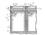
以下に本発明の実施形態における液晶表示パネルの構成を、図面を使用して説明する。はじめに本発明の第1の実施形態における液晶表示パネルの構成を、図1と図2とを使用して説明する。図1は、本発明の第1の実施形態における液晶表示パネルを示す平面図である。図2は、図1の平面図のB−B線における断面を示す断面図である。以下、図1と図2とを交互に用いて本発明の第1の実施形態を説明する。
【0044】
〔第1の実施形態:図1および図2〕
第1の基板1には、タンタル(Ta)膜からなる第1の電極2と対向電極91を設ける。さらに、この第1の電極2上に第1の電極2の陽極酸化膜である酸化タンタル(Ta2 O5 )からなる非線形抵抗層3を設ける。
さらに、クロム(Cr)膜からなる第2の電極4を非線形抵抗層3上にオーバーラップするように設けて、非線形抵抗素子10を設ける。なお、この第2の電極4の一部領域は、アルミニウム(Al)膜からなる表示電極5に接続する。表示電極5は反射特性を有し、非透過性(光減衰性)である。表示電極5には、透過性を有する開口部15を有する。
【0045】
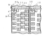
さらに、第2の基板6の上には、表示電極5と対向する領域にカラーフィルター11、12を設ける。このカラーフィルター11、12は、青色と赤色と緑色(図示せず)との3色からなる。
さらに、カラーフィルター11、12は、表示電極5の領域にて島状の複数個のカラーフィルターに分割している。この複数個のカラーフィルター間には、透過率の大きい開口部14を有している。表示電極5に設ける開口部15とカラーフィルター11、12に設ける開口部14とは異なる位置に設けてある。本実施形態においては、表示電極5の開口部15をカラーフィルター11,12と対向する部分に設けてある。
【0046】
さらに、第2の基板6には、表示電極5と対向するように透明導電性膜である酸化インジウムスズ(ITO)からなる対向電極9を設ける。対向電極9と複数個のカラーフィルター11、12、13との間には絶縁性保護膜8を設ける。
さらに、対向電極9に、外部回路の信号を印加するため、対向電極9はデーター電極(図示せず)を接続する。
さらに、第1の基板1上に設ける第1の電極2は、非線形抵抗素子10を設けるために張り出している領域を設ける。そして、この張り出し領域が第2の電極4とオーバーラップして非線形抵抗素子10を構成している。
【0047】
さらにまた図1の平面図に示すように、第1の電極2と表示電極5とは、所定寸法の間隙を有している。
また、表示電極5は、液晶16を介して対向電極9と重なり合うように配置することにより、液晶表示パネルの表示画素部19となる。
対向電極9とデーター電極に外部回路より駆動波形を印加し、非線形抵抗素子10を介して、表示電極5と対向電極9との間の表示画素部19の液晶16の透過率変化により、液晶表示パネルは所定の画像表示を行う。
【0048】
さらに第1の基板1と第2の基板6とは、液晶層16の分子を規則的に並べるための処理層として、それぞれ配向膜21、21を設ける。
さらにスペーサー17によって、第1の基板1と第2の基板6とを所定の間隙寸法をもって対向させ、第1の基板1と第2の基板6との間には、液晶16を封入する。
さらに、液晶層16は、液晶とモノマーとの混合液晶層よりなり、液晶層16に紫外線を照射することのより、モノマーからポリマーへの架橋反応を起こし、液晶とポリマーとの屈折率の差が発生し、散乱性を発生する。
【0049】
さらに、第2の基板6側より光を照射する場合には、液晶層16により光学変調と反射特性を有する表示電極5からの反射光により表示を行う。
また、第2の基板6側より光の照射がない、いわゆる暗いところでの液晶表示パネルの利用の場合には、第1の基板1上に補助光源20を設けているため、表示電極5の開口部15を通過する補助光源20の光を利用し液晶の光学特性変化を利用して、表示を行う。
【0050】
本発明の第1の実施形態に示す液晶表示パネルは、表示画素部19の領域のカラーフィルター11、12は、複数個の島状の構造をしている。
そのために、表示電極5の開口部14bは、第1の基板1側から紫外線を照射する際には、大きな透過率を示し、カラーフィルター11,12に設ける開口部14は、第2の基板6側より紫外線を照射する場合に大きな透過率を示すため、ポリマーを有する液晶層16に大きな紫外線を照射することが可能となる。
【0051】
さらに、島状のカラーフィルター間に設ける開口部14を表示画素部19上に設けているため、液晶層16に電圧を印加できる。そのため、光学変化が可能なため、開口部14を設けてもコントラスト比をほとんど低減することはない。
さらに、第2の基板6側より外部光源(図示せず)からの光の照射がないか、または弱い場合に第1の基板1側の補助光源20により液晶層16を介して第2の基板6側の観察者へ情報を表示するため、表示電極5の開口部15を設けることにより、補助光源20の光を透過することができる。さらに、表示電極5の開口部15に対向する第2の基板6上にはカラーフィルター11、12を設けているため、カラー表示が可能となる。
【0052】
以上の説明から明らかなように、本発明の第1の実施形態に示す構成からなる液晶表示パネルを用いることにより、明るい表示特性を有する液晶表示パネルを得ることが可能となると同時に、液晶層16への光照射(紫外線)照射を行う場合に、第1の基板1の液晶層16と面する逆の面より紫外線を照射する際には、表示電極5(反射板)に設ける開口部15を利用することにより、液晶層16へ効率良く紫外線を照射することができる。
さらに、表示電極5と異なる位置にあるカラーフィルターに設ける開口部14を利用することにより、表示電極の開口部14では紫外線の照射が不完全な領域にも紫外線を照射することができるため、とくに液晶層16への紫外線照射が必要な液晶層16を有する液晶表示装置においては非常に有効である。
【0053】
すなわち、従来技術の反射特性(非透過性)を有する表示電極5の場合に開口部15を設けていない場合には、まず補助光源20の光を液晶層16を介して第2の基板6側へ透過することができかかった。
同様に、補助光源20の代わりに紫外線光源を用いて液晶層16へ紫外線を照射する際にも、液晶層16へは紫外線を照射することが難しかった。
逆にカラーフィルター11においても、特に青色のカラーフィルターでは、紫外線を吸収するため、液晶層16への紫外線照射が難しかった。そのため、本第1の実施形態に示す構造を利用し、第1の基板1側に設ける開口部15と第2の基板6側に設ける開口部14を用いることにより、補助光源20の利用を可能にすることと、液晶層16への紫外線照射を可能にすることができる。
【0054】
〔第2の実施形態:図3および図4〕
つぎに、本発明の第2の実施形態における液晶表示パネルの構成を、図3と図4とを使用して説明する。図3は、本発明の第2の実施形態における液晶表示パネルを示す平面図である。図4は、図3の平面図のC−C線における断面を示す断面図である。以下、図3と図4とを交互に用いて本発明の第2の実施形態を説明する。
【0055】
第1の基板1には、タンタル(Ta)膜からなる第1の電極2と信号電極35を設ける。さらに、この第1の電極2上に第1の電極2の陽極酸化膜である酸化タンタル(Ta2 O5 )からなる非線形抵抗層3を設ける。
さらにクロム(Cr)膜からなる第2の電極4を非線形抵抗層3上にオーバーラップするように設けて、非線形抵抗素子10を設ける。なお、この第2の電極4の一部領域は、透明導電性膜として酸化インジウムスズ(ITO)からなる表示電極5と接続している。
【0056】
第2の基板6上には、第1の基板1に形成するそれぞれの表示電極5の隙間からの光の漏れを防止するために、酸化クロム膜(CrO)とクロム膜(Cr)の2層からなるブラックマトリクス7を設けてある。
さらに、第2の基板6上にはブラックマトリクス7の一部と重なり、表示電極5と対向する領域にカラーフィルター11、12、13を設ける。このカラーフィルター11、12、13は、青色と赤色と緑色との3色からなる。
さらに、カラーフィルター11、12、13は、表示電極5の領域にて各14個の島状の複数個のカラーフィルターに分割している。この複数個のカラーフィルター間には、高透過率を示す開口部14を有している。
【0057】
さらに、第2の基板6には、表示電極5と対向するように透明導電性膜である酸化インジウムスズ(ITO)からなる対向電極9を設ける。対向電極9と複数個のカラーフィルター11、12、13との間には絶縁性保護膜8を設ける。
さらに、対向電極9に、外部回路の信号を印加するため、対向電極9はデーター電極(図示せず)を接続する。
さらに、第1の基板1上に設ける第1の電極2は、非線形抵抗素子10を設けるために張り出している領域を設ける。そして、この張り出し領域が第2の電極4とオーバーラップして非線形抵抗素子10を構成している。
【0058】
さらにまた図3の平面図に示すように、第1の電極2と表示電極5とは、所定寸法の間隙を有している。
表示電極5は、液晶層16を介して対向電極9と重なり合うように配置することにより、液晶表示パネルの表示画素部19となる。
【0059】
信号電極91とデーター電極に外部回路より駆動波形を印加し、非線形抵抗素子10を介して、表示電極5と対向電極9との間の表示画素部19の液晶層16の透過率変化により、液晶表示パネルは所定の画像表示を行う。
さらに第1の基板1と第2の基板6とは、液晶層16の液晶分子を規則的に並べるための処理層として、それぞれ配向膜15、15を設ける。
【0060】
さらにスペーサー17によって、第1の基板1と第2の基板6とを所定の間隙寸法をもって対向させ、第1の基板1と第2の基板6との間には、液晶を封入する。
またさらに、第1の基板1上に偏光板18と補助光源部20とを設け、第2の基板6上に偏光板18を設ける。液晶表示パネルは自己発光しないため、光源が必要となる。この補助光源20を利用し液晶の光学特性変化を利用して、表示を行う。
【0061】
本発明の第2の実施形態に示す液晶表示パネルは、表示画素部19の領域のカラーフィルター11、12、13は、複数個の島状の構造をしている。
そのため、たとえば1個の表示画素部19の領域の赤のカラーフィルター11には、高透過率特性を有する開口部14を設けている。そのため、開口部14では、大きな光を透過できる。
さらに、島状のカラーフィルター間に設ける開口部14を表示画素部19上に設けているため、液晶層16に電圧を印加できる。そのため、光学変化が可能なため、開口部14を設けてもコントラスト比をほとんど低減することはない。
【0062】
以上の説明から明らかなように、本発明の第2の実施形態に示す構成からなる液晶表示パネルを用いることにより、明るい表示特性を有する液晶表示パネルを得ることが可能となる。
【0063】
〔第3の実施形態:図5および図6〕
つぎに本発明の第3の実施形態における液晶表示パネルの構造を、図5と図6とを用いて説明する。図5は本発明の第3の実施形態における液晶表示パネルを示す平面図である。図6は図3の平面図のD−D線における断面を示す断面図である。以下、図5と図6とを交互に用いて本発明の第3の実施形態を説明する。
【0064】
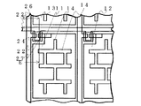
第1の基板1上には、タンタル(Ta)膜からなるゲート電極22を設ける。さらに、このゲート電極22上にゲート電極22の陽極酸化膜である酸化タンタル(Ta2 O5 )からなるゲート絶縁膜263設ける。
さらにゲート絶縁膜23上とその周囲にアモルファスシリコン(a−Si)からなる半導体層24を設ける。
【0065】
さらに、半導体層24上には、アモルファスシリコンに不純物を添加したN型アモルファスシリコン(N型a−Si)25をゲート電極22と一部重なるように設ける。
さらにN型アモルファスシリコン25上には、モリブデン(Mo)からなるソース電極26とドレイン電極27を設ける。ソース電極26は、外部信号を印加するために、データー電極(図示せず)と接続し、ドレイン電極27は、透明導電性膜である酸化インジウムスズ(ITO)膜からなる表示電極5と接続する。さらに、半導体層24上のソース電極26とドレイン電極27の間には、半導体層24の特性劣化を防止するために、保護絶縁膜51を設ける。
【0066】
第2の基板6上には、第1の基板1に形成するそれぞれの表示電極5の隙間からの光の漏れを防止することと、半導体層24への光の入射を防止するために、クロム膜(Cr)からなるブラックマトリクス7を設けてある。
さらに、第2の基板6上にはブラックマトリクス7の一部と重なり、表示電極5と対向する領域にカラーフィルターを設ける。カラーフィルター11、12、13は青色と赤色と緑色との3色からなる。
【0067】
さらに、カラーフィルター11、12、13は、表示電極5の領域にて各11個の島状の複数個のカラーフィルターに分割している。この複数個のカラーフィルター11、12、13の間には、ブラックマトリクス7の設けていない開口部14を有している。
【0068】
表示画素部19上の開口部14は蛇行する配置を有している。本発明の第3の実施形態では、X軸の方向のみ蛇行している配置を有しているが、Y軸のみまたはX軸をY軸の両方の軸に関して蛇行しても当然有効である。
この蛇行することにより、開口部14の透過率の高い領域の連続性を防止できるため、カラーフィルター11、12、13と開口部14との混色性の向上ができる。本実施形態においては、説明しやすくするために、カラーフィルター11を11個に分割する例を示したが、さらに多くの島状にすることにより、カラーフィルター11と開口部14との混合性が改善できる。
【0069】
さらに、第2の基板6には、表示電極5と対向するように透明導電性膜である酸化インジウムスズ(ITO)からなる対向電極9を設ける。
表示電極5は、液晶16を介して対向電極9と重なり合うように配置することにより、液晶表示パネルの表示画素部19となる。
【0070】
ゲート電極22と、データー電極に接続するソース電極29とに外部回路より駆動波形を印加し、薄膜トランジスター(TFT)素子を介して、表示電極5と対向電極9との間の表示画素部19の液晶層16の透過率変化により、液晶表示パネルは所定の画像表示を行う。
【0071】
さらに第1の基板1と第2の基板6とは、液晶16の分子を規則的に並べるための処理層として、それぞれ配向膜21、21を設ける。
さらにスペーサー17によって、第1の基板1と第2の基板6とを所定の間隙寸法をもって対向させ、第1の基板1と第2の基板6との間には、液晶16を封入する。
【0072】
さらに、液晶表示パネルは自己発光しないために、液晶表示パネルの第1の基板1を観察者側に配置し、第1の基板1側の補助光源20を利用する。
さらに、第1の基板1の外側に図6の断面図に示すように、第1の基板1より偏光板18と接着層(図示せず)とを設ける。さらに、第2の基板6側には、偏光板18と反射部32と接着層(図示せず)とを設け、液晶16の光学変化を、2枚の偏光板18、18を利用して行う。
【0073】
本発明の第3の実施形態に示す液晶表示パネルは、表示画素部19の領域のカラーフィルター11、12、13は、複数個の島状の構造をしている。
そのため、たとえば1個の表示画素部19の領域の赤のカラーフィルター11には、ブラックマトリクス7を形成しない領域として開口部14を設けている。そのため、開口部14では、大きな光を透過できる。
【0074】
さらに、島状のカラーフィルター間に設ける開口部14を表示画素部19上に設けている。このため、液晶層16に電圧を印加できるため、光学変化が可能であり、開口部14を設けてもコントラスト比をほとんど低減することはない。
【0075】
さらに、反射型液晶表示パネルとして利用し、偏光板18の偏光軸をお互いに直交する方向に配置することにより、開口部14はその周辺に設けるカラーフィルターの色を反射することが可能となる。そのため、色の純度が向上できる。
【0076】
さらに、表示画素部19上のカラーフィルターの配置を蛇行する配置とし、蛇行する開口部14とすることにより、開口部14と島状のカラーフィルターとの混色性が向上し、良好な表示が得られる。
【0077】
以上の説明から明らかなように、島状のカラーフィルターの周囲に設ける開口部14を利用することにより、明るい表示特性を有する液晶表示パネルを得ることが可能となる。さらに、島状のカラーフィルターの周囲に設ける開口部14と反射部32を利用し、開口部14の周囲のカラーフィルターの一部を反射することにより明るく、しかも色純度の良好な液晶表示パネルが可能となる。
【0078】
〔第4の実施形態:図7および図8〕
つぎに本発明の第4の実施形態における液晶表示パネルの構造を、図7と図8とを用いて説明する。図7は本発明の第4の実施形態における液晶表示パネルを示す平面図である。図8は図7の平面図のE−E線における断面を示す断面図である。以下、図7と図8とを交互に用いて本発明の第4の実施形態を説明する。
【0079】
第1の基板1上には、タンタル(Ta)膜からなるゲート電極22と対向電極9を設け、このゲート電極22上にゲート電極22の陽極酸化膜である酸化タンタル(Ta2 O5 )からなるゲート絶縁膜22を設ける。
さらにゲート絶縁膜23上とその周囲にアモルファスシリコン(a−Si)からなる半導体層24を設ける。
さらに、半導体層24上には、アモルファスシリコンに不純物を添加したN型アモルファスシリコン(N型a−Si)25がゲート電極22と一部重なるように設ける。さらに、N型アモルファスシリコン25上には、モリブデン(Mo)からなるソース電極26とドレイン電極27を設ける。ソース電極26は、外部信号を印加するために、対向電極9と接続し、ドレイン電極27は、透明導電性膜である酸化インジウムスズ(ITO)膜からなる表示電極5と接続する。
【0080】
さらに、半導体層24上のソース電極26とドレイン電極27の間には、半導体層24の特性劣化を防止するために、保護絶縁膜51を設ける。第2の基板6上には、ブラックマトリクスは設けていない。
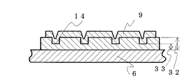
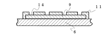
さらに、第2の基板6上には、表示電極5と対向する領域にカラーフィルターを設ける。カラーフィルター11、12、13はシアンとマゼンダとイエローとの3色からなる。
さらにカラーフィルター11、12、13は、表示電極5の領域にてカラーフィルターに光の透過する開口部14−aを有する。また、この開口部14には、ブラックマトリクスは設けない。
【0081】
さらに、図8に示すように、第2の基板6上には、ブラックマトリクスは設けていないため、カラーフィルターには開口部14があるが、表示電極5の周辺部で相互に接続している。そのため、開口部14は閉曲線の形状を有する。
さらにカラーフィルター11、12、13は、ソース電極26上まで張り出す構造を有する。この構造にすることにより表示画素部19の周囲の領域はカラーフィルターがあるため、透過率の制限が可能となる。このため、表示画素部19の表示内容に対して、非表示内容の混入を防止することが可能となる。
【0082】
さらに、第2の基板6には表示電極5と対向するように透明導電性膜である酸化インジウムスズ(ITO)からなる対向電極9を設ける。
表示電極5は、液晶層16を介して対向電極9と重なり合うように配置することにより、液晶表示パネルの表示画素部19となる。
【0083】
信号電極91とゲート電極25とに外部回路より駆動波形を印加し、薄膜トランジスター(TFT)素子を介して、表示電極5と対向電極9との間の表示画素部19の液晶16の透過率変化により液晶表示パネルは所定の画像表示を行う。
【0084】
さらに第1の基板1と第2の基板6とは、液晶16の分子を規則的に並べるための処理層として、カラーフィルター11、12、13上に配向膜21、21をそれぞれ設ける。
そのうえさらに、カラーフィルターに設ける開口部14上には、配向膜21、21とは異なる配向膜30を設ける。
【0085】
本発明の第4の実施形態においては、カラーフィルター上に設ける配向膜21は液晶分子の吸収軸が第1の基板1側では7時30分の方向を向いており、第2の基板6側では4時30分の方向を向くように処理してある。すなわち、液晶層16は90゜の角度にツイストしている。
【0086】
さらに開口部14に設ける配向膜30は、配向膜21の配向処理方向とは逆に液晶分子の吸収軸が第1の基板1側では4時30分の方向を向いており、第2の基板6側では7時30分の方向を向くように処理してある。すなわち液晶層16は、90゜の角度にツイストしている。
このように配向膜21と配向膜30とを異なる方向に配向処理をおこない、異なる方向に液晶分子の吸収軸を配置することにより、観察者と液晶表示パネルの位置関係が異なっても、広視野の範囲で良好な表示が可能となる。
つまり、配向膜21の液晶分子が過剰な黒側の表示を行うときに、配向膜30の液晶分子が過剰の黒表示を行わないため、過剰な黒表示の程度が弱まるためである。
【0087】
さらにスペーサー17によって、第1の基板1と第2の基板6とを所定の間隙寸法をもって対向させ、第1の基板1と第2の基板6との間には、液晶層16を封入する。
さらに液晶表示パネルは自己発光しないために、液晶表示パネルの第1の基板1を観察者側に配置し、第1の基板1側の外部光源31を光源として利用する。さらに、第1の基板1の外側に図7の断面図に示すように、第1の基板1より偏光板18と接着層(図示せず)とを設ける。
さらに、第2の基板6側には、偏光板18と反射部29と接着層(図示せず)とを設け、液晶16の光学変化を、2枚の偏光板18、18を利用して行う。
【0088】
本発明の第4の実施形態における液晶表示パネルは、表示画素部19の領域のカラーフィルター11、12、13は、光が透過し、ブラックマトリクスのない開口部14を有する構造である。
そのため、開口部14ではカラーフィルター11、12、13に比べて大きな光を透過できる。
【0089】
さらに、カラーフィルターは、表示電極5の周囲にて開口部14がない構成のため、液晶に電圧が印加できない領域では、できる限り透過率は低下する構成となる。
さらに、カラーフィルターに設ける開口部14を表示画素部19上に設けているため、液晶層16に電圧を印加でき、光学変化が可能となる。
さらにそのうえ、カラーフィルター上の配向膜21と開口部14の領域の配向膜30の配向処理方向を異なる方向にすることにより、広範囲の視野において良好な表示を達成できる。
【0090】
〔第5の実施形態:図9、図10および図11〕
つぎに、本発明の第5の実施形態におけるカラーフィルター11と開口部14の配置の異なる実施形態を図9と図10と図11とを用いて説明する。図9は液晶表示パネルを示す平面図であり、図10と図11とは、図9の平面図のF−F線における断面図である。なお、図9の平面図には第4の実施形態と同様な符号を用いている。さらに図10と図11とは、カラーフィルター11を設ける第2の基板6とカラーフィルター11とカラーフィルターの開口部14と対向電極9の構成を示す断面図である。
【0091】
図10に示すように、第2の基板6の上には第1の基板上の表示電極(図示せず)と対向する領域にカラーフィルター11を設ける。
このカラーフィルター11には透過率が異なり、しかもこのカラーフィルター11より大きい光を透過する高透過性カラーフィルター31を設ける。この高透過性カラーフィルター31が、以上の実施形態のカラーフィルターの開口部14に対応する。
この高透過性カラーフィルター31は、有機顔料の光脱色反応または部分染色の方法により形成することができる。このカラーフィルター11と高透過性カラーフィルター31との上面に対向電極9を設ける。
【0092】
以上に示すように、図10の断面図に示す構成により、平坦性に優れたカラーフィルターの形成が可能となり、対向電極9の断線が減少できる。
さらにカラーフィルター11内に設ける高透過性カラーフィルター31の1個当たりの占める面積を微少面積にし、しかも、多くの高透過性カラーフィルター31をカラーフィルター11に設けることにより、均一でかつ明るい液晶表示パネルを得ることが可能となる。
【0093】
つぎに図11に示す液晶表示パネルの構成を説明する。図11に示すように、第2の基板6上には第1の基板上の表示電極(図示せず)と対向する領域にカラーフィルター11を設ける。このカラーフィルター11には膜厚32が異なりしかもこのカラーフィルター11より大きい光を透過する開口部14を設ける。開口部14のカラーフィルター11は、膜厚33が薄くなっている。
この開口部14のカラーフィルター11は、カラーフィルター11の部分エッチング加工方法、または部分多層カラーフィルターの形成手段により形成することができる。さらに、このカラーフィルター11と開口部14との上面に対向電極9を設ける。
【0094】
図11の断面図に示す構成により、開口部14とカラーフィルター11の膜厚の比率により液晶表示パネルの使用環境に適する明るさの液晶表示パネルを容易に得ることが可能となる。
【0095】
つぎに、図12に示す液晶表示パネルの構成を説明する。
図12に示すように、第2の基板6の上には第1の基板上の表示電極(図示せず)と対向する領域に対向電極9を設ける。この対向電極9上にカラーフィルター11を設ける。このカラーフィルター11は開口部14を有する。
【0096】
図12の断面図に示す構成により、多数の開口部14を有する多孔質カラーフィルター11や、または膜厚の厚いカラーフィルター11を用いる場合においても、対向電極9をカラーフィルター11の下層に設けることにより対向電極9の断線は発生しにくくなる。
さらに、対向電極9の形成する工程によるカラーフィルター11の変色、または透過率の低下を防止するこができる。
【0097】
つぎに、図13に示す液晶表示パネルの構成を説明する。
図13に示すように、第2の基板6の上には第1の基板上の表示電極(図示せず)と対向する領域にカラーフィルター11を設ける。カラーフィルター11には光透過性を有する凸部36を有する。この凸部36は光を散乱するために第2の基板6と反対の面で表面が荒れている。この光透過性凸部36が高透過率を有する開口部14として作用する。
【0098】
この開口部14は光感光性樹脂を回転塗布法により第2の基板6上に形成し、熱乾燥を行い硬化させ光感光性樹脂の表面を微粒子を吹き付け光感光性樹脂の表面を荒らした後、フォトリソグラフィー法により所定の形状に加工することにより形成することができる。
さらに、このカラーフィルター11と開口部14との上面に対向電極9を設ける。
【0099】
図13の断面図に示す構成により、開口部14からの光は周辺のカラーフィルター11に広がり画素部の光量が上昇し明るく、しかも均一性の良好な表示が得られる。
【0100】
〔第6の実施形態:図14、図15および図16〕
つぎに、本発明の第6の実施形態におけるカラーフィルター11と開口部14の配置の異なる他の実施形態を図14と図15と図16とを用いて説明する。図14は液晶表示パネルを示す平面図であり、図15と図16とは、図14の平面図のG−G線における断面図である。なお、図14の平面図には第4の実施形態と同様な符号を用いている。さらに、図15と図16は、カラーフィルター11を設ける第2の基板6とカラーフィルター11と開口部14と対向電極9の構成を示す断面図である。
【0101】
図15は、第2の基板6上には第1の基板上の表示電極(図示せず)と対向する領域にカラーフィルター11を設ける。このカラーフィルター11内には光を透過し、絶縁性を有する光透過性絶縁粒子34を含む。この光透過性絶縁粒子34によりカラーフィルター11に光の透過率の大きな開口部14を設けこととなる。この光透過性絶縁粒子34は、球状または円筒状または多面体とする。
このため、この光透過性絶縁粒子34によって、光をカラーフィルター11内に拡散することが可能となる。さらに、このカラーフィルター11と光透過性絶縁粒子34との第2の基板6側には対向電極9を設ける。
【0102】
図15の断面図に示す構成を作用することにより、光透過性絶縁粒子34からなる開口部14からの光は、周辺のカラーフィルター11に広がり画素部の光量が上昇し明るく、しかも均一性の良好な表示が得られる。
【0103】
つぎに図16に示す構造の液晶表示パネルを説明する。図16に示すように、第2の基板6上には第1の基板上の表示電極(図示せず)と対向する領域にカラーフィルター11を設ける。このカラーフィルター11内には光を透過し絶縁性を有する光透過性絶縁微粒子46を含む。
この光透過性絶縁微粒子46の分散度合いによって、カラーフィルター11に光の透過率の大きな光透過性絶縁微粒子46が数個凝集する部分がカラーフィルター11内において高透過率を示し、開口部14として機能する。
【0104】
光透過性絶縁微粒子46は、球状または円筒状または多面体とする。このため光透過性絶縁微粒子46によって光をカラーフィルター11内に拡散することが可能となる。
さらに、このカラーフィルター11と光透過性絶縁性微粒子46との上面に対向電極9を設ける。
【0105】
図16の断面図に示す構成により、光透過性絶縁微粒子46の凝集によるカラーフィルター11に内で発生する高透過率部である開口部14が構成される。
この光透過性絶縁微粒子46へ入射する光は、周辺のカラーフィルター11に広がり、さらにカラーフィルター11に分散する他の光透過性絶縁微粒子46がさらに光を拡散するため画素部を透過する光量が上昇し明るく、しかも均一性の良好な表示が得られる。
【0106】
〔腕時計装置説明:図17、図18、図19および図20〕
以下に本発明の液晶表示パネルと液晶表示パネルを利用する腕時計装置について図面を参照しながら説明する。図17は、本発明の反射膜(光透過減衰膜)に開口部を有する基板を有する液晶表示パネルの全体を示す平面図である。図18は、図17のH−H線における拡大断面図である。図19は、図17に示す液晶表示パネルを利用するデジタル表示型の腕時計装置の平面模式図である。図20は、図19のI−I線における断面模式図である。以下に図17と、図18と、図19と、図20とを交互に用いて第7の実施形態を説明する。
【0107】
液晶表示パネルは、紙面下面に設ける第1の基板1と紙面上面に設ける第2の基板6を有する。第1の基板1上には、金属膜として金(Au)膜からなる遮光膜50と複数の開口部15とを有する。
図18に示すように、また、第1の基板1上には、金属膜と信号電極5との電気的短絡を防止するために、保護用絶縁膜51としてポリイミド樹脂を印刷法にて設ける。
第1の基板1と所定の間隙を有して対向する第2の基板6上には、対向電極9として7分割の電極52、53、54、55、56、57、58を設ける。7分割の電極52から58により数字等の表示が可能となる。
【0108】
また、第2の基板6上には、第1の基板1上の信号電極5を第2の基板6上へ電気的に配置転換を行うための接続電極59を有する。第1の基板1上の信号電極5の形状は、第2の基板6上に設ける対向電極を覆う領域に設けてある。
また、信号電極5は、接着材と導電粒60により、信号電極5に接続する接続部49において、第2の基板6上の接続電極59に接続する。
【0109】
図18に示すように、金属膜からなる遮光膜50には、複数の開口部15を有し、開口部15は、対向電極52から58と信号電極5との重なり合う領域に設けてあり、表示画素部19となる。
また、第1の基板1と第2の基板6との間には、液晶とモノマーの混合液晶層16を注入した後に紫外線を第2の基板6側より照射し、ポリマーとする。液晶層16は、第1の基板1と第2の基板6とシール部61と封口材(図示せず)とにより封入されている。
さらに、図18に示すように、液晶表示パネルを第1の基板1側より補助光源20により光を照射し、表示を行う場合には、遮光膜50に設ける複数の開口部15からの光の透過により表示を行うことができる。
【0110】
以上の構成を有する液晶表示パネルを腕時計装置に利用する実施形態を図19と図20とを用いて説明する。腕時計装置は、時計ケース62には、風防ガラス63と裏蓋部64を有する。
風防ガラス63側より、第2の基板6と液晶層16とシール材61と第1の基板1とを配置する。第1の基板1の下面には、液晶表示パネルを駆動する回路基板65上に補助光源20としてエレクトロルミネッセント(EL)ライトを実装し、さらに回路基板65と液晶表示パネルとの電気接続は、ストライプ上の導電性と非導電性を繰り返し積層するゼブラゴム67により行う。
【0111】
回路基板65の一部には回路基板65へのエネルギー供給源として電池66が実装してある。また、図19に示すように、液晶表示パネルにより、午前と午後の表示75と時表示76と分表示77の表示ができる。また、時刻合わせ等を行うための設定端子用入力部78を有する。
【0112】
以上の説明で明らかなように、腕時計装置の風防ガラス63の方向より外部光の照射がある場合には、外部光が腕時計装置の風防ガラス63→第2の基板6→液晶層16を経由して、第1の基板1上の金属遮光膜(反射膜)50に入射する。
外部光は、金属遮光膜50により反射され、入射経路と逆の経路により、風防ガラス63側に出射する。
この場合に、回路基板65からの情報が第2の基板6上の対向電極9に供給され、所定の表示を行い、非表示部と表示部(表示画素部19)との光学的差分により腕時計装置の観察者へ情報を提供することができる。
【0113】
逆に、外部光の強度が弱い場合には、腕時計装置の補助光源20であるELライトからの光が、第1の基板1上の金属遮光膜50の複数の開口部15を透過し、
液晶を経由し、観察者側へ出射される。また、ELライトの色彩を黄色にすることにより外部光を利用した場合と近い色彩をだすことが可能となる。
【0114】
以上の説明から明らかなように、外部光の強度が強い場合には、金膜からなる金属遮光膜による金色の反射光を得ることができる。そのため、装飾性が重要である腕時計装置においては、非常の高級感のある表示が達成できる。
また、液晶層8に液晶とポリマーからなる高分子散乱型液晶を利用することにより、非表示の際の散乱性と表示の際の高透過性を充分に利用し、非表示領域においては、液晶層16の散乱性のために、白味のある金色の反射光が得られ、表示部では、金属光沢を有する金色を表示することが可能となる。
【0115】
さらに外部光が弱いときには、補助光源20を利用し、金属遮光膜71の複数の開口部15を利用し、表示を行うことができる。
この実施形態においては、反射光の際の表示に重点を置き、複数の開口部15の個数を少なめにしているため、信号電極5と対向電極9の重なり合う領域以外には、開口部15を設けていない。そのため、開口部15の個数が少なくとも表示部の情報が認識できる。
【0116】
以下に、色々は実施形態を図面に基づいて説明する。以下に示す断面図は、第7の実施形態におけるH−H線における断面図に相当する。まづ、第8の実施形態を図21を用いて説明する。
【0117】
液晶表示パネルの第1の基板1上には、銀(Ag)薄膜からなる遮光膜(光透過減衰膜)50と遮光膜50に設ける複数の開口部15と、金属膜の遮光膜50と信号電極5との電気的短絡と銀薄膜の劣化を防止するために、保護用絶縁膜51としてポリイミド樹脂を印刷法にて設ける。
第1の基板1と所定の間隙を有して対向する第2の基板6上には、対向電極9を所定の形状の設ける。
【0118】
本第8の実施形態の特徴は、第1の基板1上の第1の遮光膜50に設ける複数の開口部15と第1の基板1の第1の遮光膜50と反対の面(裏面)上に開口部15とほぼ一致する位置に第2の遮光膜80を形成する。
さらに、補助光源20として有機エレクトロルミネッセント(EL)ランプとレンズフィルム79とを有する。レンズフィルム79は、ELランプの光を開口部15に対して垂直に出射する特性を有する。また、レンズフィルム79に色フィルターを設けることにより、補助光源20の色を変換して表示に利用することが可能である。
【0119】
裏面に設ける第2の遮光膜80は、金属膜を3から30ナノメートル(nm)形成し、半透過膜からなる。そのため、第2の基板6上から外部光が入射する場合には、第1の遮光膜50は、反射率が大きく、明るい反射特性を有する。第2の遮光膜80は、第1の遮光膜50の開口部15からの光を一部反射する。
さらに観察者と外部光との位置を実験した際の、表示領域が小さい場合には、第1の遮光膜50の開口部15の位置に対して、第2の遮光膜80の位置を周囲にずらして配置しても第2の遮光膜80の効果が得られた。また、腕時計装置の位置と開口部15と第2の遮光膜80の位置により、外部光の入射は、腕時計装置の6時側からは入射光が少ないことがわかった。
【0120】
そのため、第1の遮光膜50の開口部15に対して第2の遮光膜80は、6時側にずらす方法を採用した。
また、補助光源20は、レンズフィルム79を使用しているため、第1の遮光膜50の開口部15と第2の遮光膜80のずれた部分より光を観察者側に出射することができる。そのため、第2の遮光膜80を設けない場合に比較し、外部光の強度の強い場合には、第1の遮光膜50と第2の遮光膜80により良好な表示品質を達成でき、さらに、補助光源20を利用する場合においても、明るい表示を達成できる。
さらに、この実施形態においては、ELライトと色フィルムとの組み合わせで補助光源20の色を調節できる。
【0121】
〔第9の実施形態:図22〕つぎに、第9の実施形態について図22を用いて説明する。液晶表示パネルの第1の基板1上には、アルミニウム(Al)薄膜からなる遮光膜50と遮光膜50上に設ける複数の開口部15と、金属膜の遮光膜50と信号電極5との電気的短絡と銀薄膜の劣化を防止するために、保護用絶縁膜51としてポリイミド樹脂を印刷法にて設ける。第1の基板1と所定の間隙を有して対向する第2の基板6上には、対向電極9と色表示を行うためのカラーフィルターとを所定の形状の設ける。カラーフィルターは、青カラーフィルターとする。
【0122】
また、第1の基板1の裏面には、補助光源20としてエレクトロルミネッセント(EL)ライトと散乱板90とを配置する。
さらに、第1の基板1上に設ける遮光膜50に設ける複数の開口部15は、信号電極5と対向電極9との重なり合う表示画素部19の密度をその周辺の非表示部121の開口部15の密度を少なくしている。さらに、液晶層16は、液晶とモノマーとの混合液晶で、第1の基板1と第2の基板6との間隙に封入後に紫外線によりポリマーにする。
従来の遮光膜50に開口部15を設けない場合には、第1の基板1側では、遮光膜50により紫外線は遮蔽され、第2の基板6側は、カラーフィルター11により紫外線が非常に減衰してしまう。しかし、本第9の実施形態においては、遮光膜50に複数の開口部15を設け、さらに、表示部81と非表示部82の両方に開口部を設けることにより、モノマーからポリマーへの架橋反応を行うことができる。
【0123】
さらに、本液晶層16の液晶とポリマーの状態は、液晶層16へ印加する電圧が小さい場合に、透明で、電圧を大きくすると散乱するモードを利用する。そのため、非表示部82は外部光が強い場合に、各角度により多少異なるが、遮光膜50が鏡面のため、散乱部が明るく見える。
外部光が弱い場合には補助光源20と散乱板90により、非表示部82が散乱され暗く、表示部81が透過光によりカラーフィルター11の色の表示となる。
【0124】
〔第10の実施形態:図23〕
つぎに、第10の実施形態について図23を用いて説明する。
液晶表示パネルは、第1の基板1上には、アルミニウム(Al)薄膜と酸化アルミニウム(Al2O5 )膜と透明導電膜(酸化インジウム酸化スズ膜ITO)との多層膜からなる遮光膜50を設ける。多層膜の干渉効果により金色を得ることができる。
さらに、遮光膜50には、複数の開口部15を有し、多層膜の遮光膜50と信号電極5との電気的短絡を防止するために、保護用絶縁膜51としてポリイミド樹脂を印刷法にて設ける。第1の基板1と所定の間隙を有して対向する第2の基板6上には、対向電極9を所定の形状の設ける。
【0125】
本第10の実施形態の特徴は、第1の基板1上の第1の遮光膜50に設ける複数の開口部15と第1の基板1の第1の遮光膜50と反対の面(裏面)に所定の間隙を介して設ける散乱板90と散乱板90上に設ける第2の遮光膜80とを有する。遮光膜80に設ける開口部50とほぼ一致する位置に第2の遮蔽膜80を設ける。
さらに補助光源20としてライトルミネッセントランプ(LED)20を液晶表示パネルの周囲に設け、さらにLEDを表示部に照射するために、散乱板90は、導光板としての効力を有し、さらに第1の基板1と散乱板90とは、LEDの光を液晶表示パネルの全体に照射するために所定の間隙を有して配置する。
【0126】
散乱板90上に金属製の第2の遮光膜80を設けることにより、外部光による反射特性は充分であり、さらに、液晶表示パネルの周囲からのLEDからの光に対してはより効率良く、第2の基板6の方向に光りを出射することが可能となり、
液晶表示パネルの周囲よりの補助光源20に対しては非常に有効となる。
【0127】
〔第11の実施形態:図24〕
つぎに、第11の実施形態について図24を用いて説明する。
液晶表示パネルの第1の基板1上には、信号電極5として、透明導電膜である酸化インジウム酸化スズ(ITO)膜を設ける。第11の実施形態においては、第1の基板1上には、遮光膜は設けていない。
また、第1の基板1と所定の間隙を有して対向する第2の基板6上には、対向電極9を所定の形状の設ける。第1の基板1と第2の基板6との間隙には、架橋構造のポリマーを含む液晶を封入してある。信号電極5と対向電極9上には液晶を配列するための配向膜は設けていない。
【0128】
この第11の実施形態の特徴は、第1の基板1上に遮光膜(光透過減衰膜)は設けず、第1の基板1の裏面側に所定の間隙を設けて、遮光膜50を設ける。
遮蔽膜50には、複数の開口部15を有し、補助光源20からの光を第2の基板6側に出射する構造とする。この場合に、補助光源20に対する開口部15の相対位置と、表示部と外部光と開口部15との相対位置とが異なり、開口部15が表示部に対して深いため、比較的開口部15の表示に対する影響は少なく、また補助光源20からの出射光は、充分に観察者に認識できた。
【0129】
さらに、液晶層16と遮蔽膜50との距離があるため、微細な表示には2重像のために不向きであるが、液晶層16の前方散乱特性が利用できる点と、第1の基板1と遮蔽膜50との間隙の媒体の屈折率により非表示部の液晶層16の散乱特性が向上し、表示部とのコントラストの優れた表示が可能となる。
【0130】
〔第12の実施形態:図25、図26、図27および図28〕
つぎに、本発明の第12の実施形態における液晶表示パネルと液晶表示パネルを利用する腕時計装置について図25を参照しながら説明する。第12の実施形態は、対向電極9をM本有し、信号電極5もN本有し、MxNのマトリクス型の液晶表示パネルの例である。マトリクス型の液晶表示パネルには、各対向電極9と信号電極5の交点が各表示画素部19となる。各表示画素部19にスイッチング素子を有するアクティブマトリクス型とスイッチング素子を設けないパッシブマトリクス型とがある。本実施形態はどちらにも有効であるが、パッシブマトリクス型を用いて説明する。
【0131】
図25は、本発明の第12の実施形態における液晶表示パネルの全体図を示す平面図である。図26は、図25のJ−J線における拡大断面図である。図27は、図25に示す液晶表示パネルを利用するデジタル表示と分針と時針とを有するアナログ型の両方を有するコンビネーション型の腕時計装置の平面模式図である。図28は、図27のK−K線における断面模式図である。以下に図25、図26、図27と図28とを交互に用いて第12の実施形態を説明する。
【0132】
液晶表示パネルは、紙面下面に設ける第1の基板1と紙面上面に設ける第2の基板6を有する。第1の基板1上には、金属膜として金(Au)膜からなる遮光膜50と複数の開口部15とを有する。開口部15は、第1の基板1のほぼ全面に設ける。
また、第1の基板1上には、金属膜と信号電極5との電気的短絡を防止するために、保護用絶縁膜51としてポリイミド樹脂を印刷法にて設ける。
信号電極5は、図25に示すように、N本のストライプ電極であり、図26の断面図に示すように、第1の基板1の外周部まで設ける。また、第1の基板1と所定の間隙を有して対向する第2の基板6上には、対向電極9をM本のストライプ電極として設ける。
【0133】
また、第2の基板6上には、第1の基板1上に設ける遮蔽膜50の開口部15とほぼ対向する位置に設ける複数の島状のカラーフィルター11と遮蔽膜50の開口部15と異なる位置に設けるカラーフィルター11の開口部14とを有し、さらに絶縁性保護膜8と対向電極9とを有する。以上により明るいカラー表示と液晶層16への紫外線等の照射が可能な構造となる。
【0134】
また、腕時計装置の場合には、回路基板65と液晶表示パネルの電気的接続を行う実装容積に非常に制限あるため、第1の基板1上のストライプ状の信号電極5をシール材61に導電粒60を混ぜ、信号電極5と導電粒60と第2の基板6上に設けるストライプ状の接続電極59により、第2の基板6上に電気的に配置転換を行う。
この構造を採用することにより、回路基板65は、液晶表示パネルに対して単一面にのみ実装を行うのみでよいため、実装容積を非常に小さくすることができる。
【0135】
また、第1の基板1と第2の基板6の間隙には、第1の基板1の外周部にシール部61を有し、以上の空間に液晶とモノマーを有する液晶層16を注入後、注入口を封口材68にて注入口を封止する。
また、図26に示すように、第1の基板1に設ける遮光膜50の開口部15により、補助光源20からの光を液晶層16を介して風防ガラス側に出射する。そのため、各表示画素部19を構成する信号電極5と対向電極9の交差領域には、それぞれ複数の開口部14bを有する。
【0136】
〔腕時計装置説明:図27および図28〕
以上の構成を有する液晶表示パネルを腕時計装置に利用する実施形態を図27と図28とを用いて説明する。
腕時計装置は、時計ケース62には、風防ガラス63と裏蓋部64を有する。風防ガラス63側より、第2の基板6と液晶層16とシール材61と第1の基板1とを配置する。液晶表示パネル中央には、アナログ時計の分針69と時針70とを駆動する指針軸84が貫通し、さらに、第1の基板1の下面には、アナログ時計部を駆動する機械駆動部73を有する。また、機械駆動部73の下面には、液晶表示パネルを駆動するデジタル回路部65と電源回路と電池96がある。
【0137】
また、液晶表示パネルの第2の基板6上には、腕時計装置として使用している場合に液晶層16への紫外線の入射と反射光の制限を行うと同時に、アナログ時計の時刻を示す数字71を有する時板72を設ける。
時板72と液晶層16への紫外線遮蔽膜を兼用することにより、腕時計装置のように、非常の厚さの限定をするものに関しては、有効な方法である。
さらに回路基板65と液晶表示パネルとの電気接続は、ストライプ上の導電性と非導電性を繰り返し積層するゼブラゴム67により行う。
【0138】
また図27に示すように、液晶表示パネルにより、年表示85と、月表示86と日表示89のモード変更を行うモード切り替えボタン87と、時刻合わせ等を行うための設定端子用入力部78を有する。
さらに、液晶表示パネルへの補助光源20は、白色LEDを利用し、LEDランプ点灯ボタン88のより点灯する。LEDは、LED接続線74により、電源回路基板へ接続している。
【0139】
以上の説明より明らかなように、腕時計装置の風防ガラス63の方向より外部光の照射がある場合には、外部光が腕時計装置の風防ガラス63→時板72→第2の基板6→カラーフィルター11→液晶層16を経由して、第1のの基板1上の金属遮光膜50に入射する。
外部光は、金属遮光膜50により反射され、入射経路と逆の経路により、風防ガラス側63に出射する。この場合に、回路基板65からの情報が第2の基板6上の対向電極9と信号電極5とに供給され、所定の表示を行い、光学的差分により腕時計装置の観察者へ情報を提供することができる。
【0140】
逆に、外部光の強度が弱い場合には、腕時計装置の補助光源20であるLEDライトからの光が、第1の基板1上の金属遮光膜50の複数の開口部15を透過し、液晶層16を経由し、観察者側へ出射される。またLEDライトの色彩を白色にすることにより外部光を利用した場合と近い色彩をだすことが可能となる。
【0141】
以上の説明から明らかなように、外部光の強度が強い場合には、金属膜からなる金属遮光膜(反射膜)による金色の反射光を得ることができる。
そのため、装飾性が重要である腕時計装置においては、非常の高級感のある表示が達成できる。
また、液晶層16に液晶とポリマーからなる高分子散乱型液晶を利用することにより、非表示の際の散乱性と表示の際の高透過性を充分に利用し、非表示領域においては、液晶層8の散乱性のために、白味のある金色の反射光が得られ、表示部では、金属光沢を有する金色を表示することが可能となる。
さらに、外部光が弱いときには、補助光源20を利用し、金属遮光膜50の複数の開口部15を利用し、表示を行うことができる。
【0142】
【発明の効果】
本発明の液晶表示パネルは、第1の基板上に設ける信号電極と、第2の基板上に設ける対向電極と、第1の基板と第2の基板との間に封入する液晶とを備え、信号電極と対向電極との交点に複数の画素部を有し、少なくとの第1の基板の信号電極を有する面、または信号電極を有する面と逆の面に遮光膜を有し、遮光膜の各画素部に開口部を有するため、遮光膜を設けていない基板上にカラーフィルターを設け、液晶表示パネルへ紫外線等との遮光が液晶層の両面にある場合においても、開口部により光の照射を可能とする。特に液晶層にモノマーを含み、紫外線により、ポリマーに架橋反応を行う場合には、開口部は非常に有効である。
【0143】
さらに、遮光膜を液晶層に面する面と反対の面に設けることにより、開口部と液晶層が基板の厚み分離れるため、開口部の面積を相対的に大きくすることが可能となる。また、開口部への補助光源より光りを照射する場合に、基板を透明とすることにより基板を導光板として利用することが可能となる。
さらに、開口部と基板とを所定の間隙を設けて配置することにより、補助光源からの光を開口部に均一に照射することが可能となる。
【0144】
また、基板の液晶層に面する基板上に開口部を設け、逆の面上には、開口部に遮光膜を設ける。または基板と間隙を有する部分に遮光板を設けることにより、非表示の際の均一性が向上する。
また、遮光膜、または遮光板に金属色、たとえば、金薄膜、銀薄膜、白金薄膜を利用することにより、装飾性に優れた表示が可能となる。また、カラフルな色フィルターとの組み合わにより表示の他品種化が可能となる。
【0145】
また、遮光膜、または遮光板の全面に小さな開口部を形成し、さらに、開口部に光学素子を形成し、外光に対しては、反射し、補助光源に関しては、透過光を散乱することにより、コントラストの良い表示ができる。
【0146】
本発明の液晶表示パネルの構成である表示電極に設けるカラーフィルターに開口部を設ける構造か、または複数の島状のカラーフィルターとし、しかもその複数の島状のカラーフィルター間にカラーフィルターを設けない開口部を設けることにより、明るい表示性能を有するカラー表示可能な液晶表示パネルを得ることが可能となる。
【0147】
さらに、本発明の液晶表示パネルの構成を第1の基板または第2の基板に反射部を有する液晶表示パネルに使用することにより、カラーフィルターに設ける開口部の良好な透過率と、開口部の周囲のカラーフィルターを開口部を利用し反射部から部分的に反射できるため、明るくかつ色純度の良好な表示が可能となる。
【0148】
さらに、カラーフィルター上の配向膜と開口部上の配向膜の特性を変えることにより、開口部の透過率の高さを利用し、島状のカラーフィルター上の表示性能の低下を防止できる。
さらに、カラーフィルターと開口部の透過率の差を可変することにより、液晶表示パネルの使用環境に対応する明るさを有する液晶表示パネルを得ることが可能となる。
【0149】
以上に説明した第1の実施形態から第5の実施形態に関しては、第1の基板上に非線形抵抗素子を有するときの例を示してあるが、非線形抵抗素子のない単純に第1の基板上に設ける対向電極と第2の基板上に設ける対向電極を備え、対向電極と対向電極との交点に複数の画素部(表示画素部)を有する単純マトリクス構成の液晶表示パネルにおいても、液晶の透過率変化を表示に使用する。このため以上説明した本発明の第1の実施形態から第3の実施形態における効果は得られる。
【図面の簡単な説明】
【図1】本発明の第1の実施形態における液晶表示パネルを示す平面図である。
【図2】本発明の第1の実施形態における液晶表示パネルを示す断面図である。
【図3】本発明の第2の実施形態における液晶表示パネルを示す平面図である。
【図4】本発明の第2の実施形態における液晶表示パネルを示す断面図である。
【図5】本発明の第3の実施形態における液晶表示パネルを示す平面図である。
【図6】本発明の第3の実施形態における液晶表示パネルを示す断面図である。
【図7】本発明の第4の実施形態における液晶表示パネルを示す平面図である。
【図8】本発明の第4の実施形態における液晶表示パネルを示す断面図である。
【図9】本発明の第5の実施形態における液晶表示パネルを示す平面図である。
【図10】本発明の第5の実施形態における液晶表示パネルを示す断面図である。
【図11】本発明の第5の別の実施形態における液晶表示パネルを示す断面図である。
【図12】本発明の第5の別の実施形態における液晶表示パネルを示す断面図である。
【図13】本発明の第5の別の実施形態における液晶表示パネルを示す断面図である。
【図14】本発明の第6の実施形態における液晶表示パネルを示す平面図である。
【図15】本発明の第6の実施形態における液晶表示パネルを示す断面図である。
【図16】本発明の第6の別の実施形態における液晶表示パネルを示す断面図である。
【図17】本発明の第7の実施形態における液晶表示パネルを示す平面図である。
【図18】本発明の第7の実施形態における液晶表示パネルを示す断面図である。
【図19】本発明の第7の実施形態における液晶表示パネルを利用する腕時計装置の平面模式図である。
【図20】本発明の第7の実施形態における液晶表示パネルを利用する腕時計装置の断面模式図である。
【図21】本発明の第8の実施形態における液晶表示パネルを示す断面図である。
【図22】本発明の第9の実施形態における液晶表示パネルを示す断面図である。
【図23】本発明の第10の実施形態における液晶表示パネルを示す断面図である。
【図24】本発明の第11の実施形態における液晶表示パネルを示す断面図である。
【図25】本発明の第12の実施形態における液晶表示パネルを示す平面図である。
【図26】本発明の第12の実施形態における液晶表示パネルを示す断面図である。
【図27】本発明の第12の実施形態に示す液晶表示パネルを利用する腕時計装置の平面模式図である。
【図28】本発明の第12の実施形態における液晶表示パネルを利用する腕時計装置の断面模式図である。
【図29】従来技術における液晶表示パネルを示す平面図である。
【図30】従来技術における液晶表示パネルを示す断面図である。
【符号の説明】
1 第1の基板
6 第2の基板
10 非線形抵抗素子
11 カラーフィルター
12 カラーフィルター
13 カラーフィルター
14 カラーフィルターの開口部
15 光透過減衰膜の開口部
19 表示画素部
20 補助光源
28 外部光源
50 遮光膜(光透過減衰膜)
51 保護膜
59 接続電極
60 導電粒
61 シール材
62 時計ケース
63 風防ガラス
64 裏蓋
65 回路基板
90 散乱板[0001]
BACKGROUND OF THE INVENTION
The present invention relates to a structure of a liquid crystal display panel, and in particular, includes a counter electrode provided on a first substrate, a signal electrode provided on a second substrate, and a liquid crystal sealed between the first substrate and the second substrate. A liquid crystal display panel having a plurality of pixel portions at the intersections of the counter electrode and the signal electrode, and applying a voltage to each pixel portion to display using the optical characteristic change of the liquid crystal, or a first substrate provided on the
Further, the present invention relates to a color liquid crystal display panel or a reflection type liquid crystal display panel having a light transmission attenuation film made of a color filter or a reflection film on a first substrate or a second substrate.
Furthermore, the present invention relates to a liquid crystal display panel using a liquid crystal layer having a liquid crystal and a polymer.
Further, the present invention relates to a liquid crystal display panel used for a timepiece device.
[0002]
[Prior art]
In recent years, the display capacity of a liquid crystal display panel using a liquid crystal panel has been increasing.
And a counter electrode provided on the first substrate, a signal electrode provided on the second substrate, and a liquid crystal sealed between the first substrate and the second substrate, and an intersection of the counter electrode and the signal electrode There is a means of using a multiplex drive in a liquid crystal display panel having a simple matrix configuration in which a plurality of pixel portions are provided and a voltage is applied to each pixel portion to perform display using a change in optical characteristics of liquid crystal.
[0003]
Furthermore, a liquid crystal display panel of active matrix means in which a nonlinear resistance element is provided in each pixel portion is employed.
The non-linear resistance element is roughly classified into a three-terminal system using a thin film transistor and a two-terminal system using a non-linear resistance element.
As this two-terminal system, a diode type, a varistor type, a TFD type, and the like have been developed.
[0004]
Furthermore, a brighter display device is required to reduce power consumption, which is an advantage of liquid crystal compared to other display devices. For this purpose, the transmittance of each pixel portion should be improved. Alternatively, there is a means for improving a so-called aperture ratio, which is a ratio between a pixel portion and a gap between each pixel portion.
In addition, a method of using the difference in refractive index of the liquid crystal for colorization is also performed, but the hue changes depending on the positional relationship between the liquid crystal display panel and the observer or the position of the pixel portion and the observer. Things happen.
Further, although a method of forming a color filter over the entire area of the pixel portion is used, it is dark, so that it is not suitable for a liquid crystal display panel in which brightness is important.
Further, when the reflective film is formed on the entire surface of the pixel portion, the light from the auxiliary light source for displaying through the reflective film is blocked.
[0005]
Furthermore, since the purpose is different between the pixel portion formed by the aggregate of the pixel portions and the parting portion provided around the pixel portion, it is necessary to control the color filter or the reflective film.
In the case of a liquid crystal layer containing a polymer in the liquid crystal, it is necessary to irradiate the liquid crystal layer with ultraviolet rays, but the color filter and the reflective film block the ultraviolet rays, and the liquid crystal layer cannot be sufficiently irradiated with ultraviolet rays. .
[0006]
Furthermore, when a pigment is contained in a liquid crystal layer containing liquid crystal and a polymer, irradiation with ultraviolet rays becomes more difficult.
[0007]
Hereinafter, the prior art will be described with reference to FIGS. 29 and 30 in the case of using a two-terminal nonlinear resistance element. FIG. 29 is a plan view showing a configuration of a liquid crystal display panel in which a color filter and a reflective film are formed over the entire pixel portion. FIG. 30 is a cross-sectional view showing a cross section taken along line AA in the plan view of FIG. The prior art will be described below using FIG. 29 and FIG. 30 alternately.
[0008]
A
Further, the
[0009]
On the other hand, the
[0010]
Further,
Further, the
[0011]
Further, a
Furthermore, in order to apply a signal of an external circuit to the
[0012]
Further, the
Furthermore, as shown in the plan view of FIG. 29, there is a gap of a predetermined dimension between the
[0013]
The
A driving waveform is applied to the
[0014]
Further, the
[0015]
Further, the
As the
[0016]
Further, an external
[0017]
In the conventional liquid crystal display panel shown in FIGS. 29 and 30, the
Therefore, for example, the
[0018]
Further, the
Furthermore, when the auxiliary
[0019]
[Problems to be solved by the invention]
As described above, when a conventional color filter or a light transmission attenuating film made of a reflective film is used, when the light from the light source is weak, the display becomes dark and the display content can hardly be recognized. Further, when both the color filter and the reflective film are used on different substrates, the use of the auxiliary light source is remarkably limited.
[0020]
Further, in the case of a reflective liquid crystal display panel, since an external light source is used and display is performed according to the optical change of the liquid crystal display panel, the brightness is further important, so that effective use of light is important.
[0021]
Furthermore, in the case of an active matrix type liquid crystal display panel having a nonlinear resistance element, the region where the nonlinear resistance element is formed shields light compared to a simple matrix type liquid crystal display panel composed of a pixel portion at the intersection region of the counter electrode and the signal electrode. Therefore, the brightness is further reduced.
[0022]
In addition, when using a polymer-scattering liquid crystal composed of a liquid crystal and polymer mixed liquid crystal that requires UV irradiation to the liquid crystal layer, UV light is applied to the liquid crystal layer by forming a color filter and a reflective film on different substrates. Inhibits.
Further, when a dye is mixed in the polymer scattering liquid crystal, it is very difficult to irradiate the polymer scattering liquid crystal with ultraviolet rays.
[0023]
(Object of invention)
An object of the present invention is to solve the above-mentioned problems, improve the transmittance even in a liquid crystal display panel having a color filter and a reflective film, provide a liquid crystal display panel having a bright display performance, and provide light to the liquid crystal layer. An object of the present invention is to provide a structure that can irradiate.
In addition, when the through holes are provided in the first substrate and the second substrate for use in a timepiece device, it is necessary to prevent the influence of the through holes from reaching the actually used display pixel portion.
[0024]
[Means for Solving the Problems]
In order to achieve the above object, the liquid crystal display panel of the present invention employs the following configuration.
[0026]
The liquid crystal display panel of the present invention includes an electrode provided on each of the first substrate and the second substrate, and a liquid crystal layer sealed between the first substrate and the second substrate. It has a pixel part at the intersection, and this pixel part is provided with a reflective film and a color filter. The reflective film is provided with an opening in the pixel part, and the color filter has a color filter around the color filter in the pixel part. Than the pixel part so that the transmittance is higher than Smaller than the opening of the reflective film An island-shaped color filter is arranged at a position that is formed in an island shape and overlaps the opening of the reflective film.
[0027]
A liquid crystal display panel of the present invention includes a counter electrode provided on a first substrate, a signal electrode provided on a second substrate, and a liquid crystal sealed between the first substrate and the second substrate, Each pixel portion of the liquid crystal display panel that has a plurality of pixel portions at the intersections of the counter electrode and the signal electrode and applies a voltage to each pixel portion to display using the change in optical characteristics of the liquid crystal includes a color filter, or Each pixel unit has a plurality of island-shaped light transmission attenuation films, and a light transmission attenuation film is formed around the plurality of island-shaped light transmission attenuation films. It has a transparent opening.
[0028]
A liquid crystal display panel of the present invention includes a counter electrode provided on a first substrate, a signal electrode provided on a second substrate, and a liquid crystal sealed between the first substrate and the second substrate, A collection of pixel units, each pixel unit of a liquid crystal display panel having a plurality of pixel units at the intersections between the counter electrode and the signal electrode, and applying a voltage to each pixel unit to display using the change in optical characteristics of the liquid crystal The parting portion provided around the display portion includes a light transmission attenuation film made of at least one of a color filter and a reflection film, and each pixel portion includes a plurality of island-shaped light transmission attenuation films. And having a plurality of island-shaped light transmission attenuation films around the plurality of island-shaped light transmission attenuation films, and also having a plurality of island-shaped light transmission attenuation films in the parting portion. An opening for transmitting light is provided around the light transmission attenuation film.
[0029]
A liquid crystal display panel of the present invention includes a counter electrode provided on a first substrate, a signal electrode provided on a second substrate, and a liquid crystal sealed between the first substrate and the second substrate, A collection of pixel units, each pixel unit of a liquid crystal display panel having a plurality of pixel units at the intersections between the counter electrode and the signal electrode, and applying a voltage to each pixel unit to display using the change in optical characteristics of the liquid crystal The parting portion provided around the display portion includes a light transmission attenuation film made of at least one of a color filter and a reflection film, and each pixel portion includes a plurality of island-shaped light transmission attenuation films. A plurality of island-shaped light transmission attenuation films, and a plurality of island-shaped light transmission attenuation films around the parting portion. The light transmission attenuation film has an opening that allows light to pass therethrough, and the opening provided in each pixel part and parting part Density is different.
[0030]
A liquid crystal display panel of the present invention includes a counter electrode provided on a first substrate, a signal electrode provided on a second substrate, and a liquid crystal sealed between the first substrate and the second substrate, Each pixel unit of a liquid crystal display panel that has a plurality of pixel units at the intersection of the counter electrode and the signal electrode and applies a voltage to each pixel unit to display using the change in optical characteristics of the liquid crystal has a color filter and a reflection A light transmission attenuation film made of a film is provided, and two types of light transmission attenuation films of each pixel portion have openings through which light is transmitted.
[0031]
A liquid crystal display panel of the present invention includes a counter electrode provided on a first substrate, a signal electrode provided on a second substrate, and a liquid crystal sealed between the first substrate and the second substrate, A first substrate is provided in each pixel portion of a liquid crystal display panel having a plurality of pixel portions at the intersections of the counter electrode and the signal electrode, and applying a voltage to each pixel portion to perform display using a change in optical characteristics of liquid crystal. It has a light transmission attenuation film made of a reflective film on top, a light transmission attenuation film made of a color filter on the second substrate, and two kinds of light transmission attenuation films of each pixel section. It has a transparent opening.
[0032]
A liquid crystal display panel of the present invention includes a counter electrode provided on a first substrate, a signal electrode provided on a second substrate, and a liquid crystal sealed between the first substrate and the second substrate, A first substrate is provided in each pixel portion of a liquid crystal display panel having a plurality of pixel portions at the intersections of the counter electrode and the signal electrode, and applying a voltage to each pixel portion to perform display using a change in optical characteristics of liquid crystal. It has a light transmission attenuation film made of a reflective film on top, a light transmission attenuation film made of a color filter on the second substrate, and two kinds of light transmission attenuation films of each pixel section. The apertures that transmit light are provided, and the apertures provided in the reflective film and the apertures provided in the color filter are distributed at different positions in each pixel unit.
[0033]
The liquid crystal display panel of the present invention has an alignment characteristic different from that of the island-shaped color filter or the alignment film on the reflective film and the alignment film on the opening.
[0034]
In the liquid crystal display panel of the present invention, the liquid crystal layer sealed between the first substrate and the second substrate is a mixture of a polymer and a liquid crystal whose monomer is crosslinked with ultraviolet rays.
[0035]
In the liquid crystal display panel of the present invention, the liquid crystal layer sealed between the first substrate and the second substrate is a mixture of a polymer and a liquid crystal in which the monomer is crosslinked with ultraviolet rays. Has a pigment.
[0036]
In the liquid crystal display panel of the present invention, the liquid crystal layer sealed between the first substrate and the second substrate is a mixture of a polymer and a liquid crystal in which a monomer is crosslinked with ultraviolet rays, and is a color filter or alignment A cross-linking structure is progressing around the opening of the membrane.
[0037]
In the liquid crystal display panel of the present invention, the first substrate and the second substrate have a through hole, and in the vicinity of the through hole, the light transmission attenuation film has an opening in the vicinity of the through hole. Does not provide an opening.
[0038]
[Action]
The light transmission attenuation film made of a color filter or a reflection film provided in each pixel portion of the liquid crystal display panel of the present invention has a structure having an opening for transmitting light or a plurality of island-shaped color filters or reflection films. In addition, a configuration having a light transmitting region around the plurality of island-shaped color filters or the reflective film is employed.
For this reason, there is light absorption by the color filter or light shielding by the reflection film, but since an opening is provided around the light transmission attenuation film, the transmittance around the light transmission attenuation film is large and a bright display is possible. Become.
[0039]
Furthermore, by distributing the positions of the color filter provided in each pixel portion and the opening of the reflective film at different positions, light having a larger transmittance than the color filter side can be transmitted in a region where the transmittance of the opening provided in the color filter is large. Is possible.
In addition, since the transmittance can be increased at a position different from the opening of the color filter by the opening provided in the reflective film, when light enters from the color filter side, the opening of the color filter Using a reflective film, light can be effectively reflected to the color filter side. Furthermore, light from the reflective film side can pass through the color filter side through the opening of the reflective film. Therefore, especially in a liquid crystal display panel having a structure in which a color filter is arranged on the viewer side and a reflective film is arranged on the light source side, light from the color filter side (external light source) and light on the reflective film side (auxiliary light source) Can be brightly displayed.
[0040]
In particular, when the monomer in the liquid crystal layer undergoes a cross-linking reaction upon irradiation with ultraviolet rays, the color filter has both ultraviolet ray shielding by a color filter and ultraviolet ray shielding by a reflective film, which significantly impedes the transmission of ultraviolet rays to the liquid crystal layer. The opening of the reflective film or the opening of the reflective film is very effective.
Furthermore, by setting the color filter opening and the reflection film opening in each pixel portion to different positions, the liquid crystal layer is irradiated with ultraviolet rays from the color filter side and ultraviolet rays from the reflection film side. The region that can be irradiated with ultraviolet rays can be increased.
[0041]
Further, in an active matrix type liquid crystal display panel having a non-linear resistance element in each pixel portion, the brightness is more important because the area of the non-linear resistance element shields light compared to a simple matrix type liquid crystal display panel.
Therefore, in a light transmission attenuation film made of a color filter or a reflection film, each pixel portion is provided with a plurality of openings, or the light transmission attenuation film is formed into a plurality of islands so that the periphery thereof is an opening. By improving the display quality, the display quality can be improved.
[0042]
Further, in the case of a liquid crystal display panel used for a timepiece device, when a pointer shaft is processed by providing an opening around the pointer shaft portion in a light transmission attenuation film made of a color filter or a reflective film. It serves as a position display.
Further, a light transmission attenuation film is provided around the periphery. This light transmission attenuation film has a parting effect. Further, in the display pixel portion around it, by providing a plurality of openings in the light transmission attenuation film provided in each pixel, the same effect as described above can be obtained.
[0043]
DETAILED DESCRIPTION OF THE INVENTION
Hereinafter, a configuration of a liquid crystal display panel according to an embodiment of the present invention will be described with reference to the drawings. First, the configuration of the liquid crystal display panel according to the first embodiment of the present invention will be described with reference to FIGS. FIG. 1 is a plan view showing a liquid crystal display panel according to the first embodiment of the present invention. 2 is a cross-sectional view showing a cross section taken along line BB in the plan view of FIG. Hereinafter, the first embodiment of the present invention will be described using FIG. 1 and FIG. 2 alternately.
[0044]
[First Embodiment: FIGS. 1 and 2]
The
Further, the
[0045]
Further,
Further, the
[0046]
Further, a
Further, in order to apply a signal of an external circuit to the
Further, the
[0047]
Furthermore, as shown in the plan view of FIG. 1, the
Further, the
A driving waveform is applied to the
[0048]
Further, the
Further, the
Furthermore, the
[0049]
Further, when light is irradiated from the
Further, in the case of using a liquid crystal display panel in a so-called dark place where there is no light irradiation from the
[0050]
In the liquid crystal display panel shown in the first embodiment of the present invention, the
Therefore, the opening 14b of the
[0051]
Further, since the
Further, when light from an external light source (not shown) is not irradiated or weak from the
[0052]
As is apparent from the above description, by using the liquid crystal display panel having the configuration shown in the first embodiment of the present invention, a liquid crystal display panel having bright display characteristics can be obtained, and at the same time, the
Further, by utilizing the
[0053]
That is, in the case of the
Similarly, when the ultraviolet light source is used instead of the auxiliary
On the contrary, in the
[0054]
[Second Embodiment: FIGS. 3 and 4]
Next, the configuration of the liquid crystal display panel according to the second embodiment of the present invention will be described with reference to FIGS. FIG. 3 is a plan view showing a liquid crystal display panel according to the second embodiment of the present invention. 4 is a cross-sectional view showing a cross section taken along line CC in the plan view of FIG. Hereinafter, the second embodiment of the present invention will be described using FIG. 3 and FIG. 4 alternately.
[0055]
The
Further, the
[0056]
Two layers of a chromium oxide film (CrO) and a chromium film (Cr) are formed on the
Further,
Further, the
[0057]
Further, a
Further, in order to apply a signal of an external circuit to the
Further, the
[0058]
Furthermore, as shown in the plan view of FIG. 3, the
The
[0059]
A driving waveform is applied to the signal electrode 91 and the data electrode from an external circuit, and the
Further, the
[0060]
Further, the
Furthermore, the
[0061]
In the liquid crystal display panel shown in the second embodiment of the present invention, the
Therefore, for example, the
Further, since the
[0062]
As is apparent from the above description, a liquid crystal display panel having bright display characteristics can be obtained by using the liquid crystal display panel having the configuration shown in the second embodiment of the present invention.
[0063]
[Third Embodiment: FIGS. 5 and 6]
Next, the structure of the liquid crystal display panel according to the third embodiment of the present invention will be described with reference to FIGS. FIG. 5 is a plan view showing a liquid crystal display panel according to the third embodiment of the present invention. FIG. 6 is a cross-sectional view showing a cross section taken along line DD in the plan view of FIG. Hereinafter, a third embodiment of the present invention will be described using FIG. 5 and FIG. 6 alternately.
[0064]
A
Further, a
[0065]
Further, an N-type amorphous silicon (N-type a-Si) 25 obtained by adding impurities to amorphous silicon is provided on the
Further, a
[0066]
On the
Further, on the
[0067]
Further, the
[0068]
The
By meandering, since the continuity of the high transmittance region of the
[0069]
Further, a
The
[0070]
A driving waveform is applied from an external circuit to the
[0071]
Further, the
Further, the
[0072]
Further, since the liquid crystal display panel does not emit light, the
Further, as shown in the cross-sectional view of FIG. 6, a
[0073]
In the liquid crystal display panel shown in the third embodiment of the present invention, the
Therefore, for example, the
[0074]
Furthermore, an
[0075]
Furthermore, by using the liquid crystal display panel as a reflective liquid crystal display panel and arranging the polarization axes of the
[0076]
Furthermore, the arrangement of the color filter on the
[0077]
As is clear from the above description, a liquid crystal display panel having bright display characteristics can be obtained by using the
[0078]
[Fourth Embodiment: FIGS. 7 and 8]
Next, the structure of the liquid crystal display panel according to the fourth embodiment of the present invention will be described with reference to FIGS. FIG. 7 is a plan view showing a liquid crystal display panel according to the fourth embodiment of the present invention. 8 is a cross-sectional view showing a cross section taken along line E-E of the plan view of FIG. Hereinafter, the fourth embodiment of the present invention will be described using FIG. 7 and FIG. 8 alternately.
[0079]
A
Further, a
Further, an N-type amorphous silicon (N-type a-Si) 25 obtained by adding impurities to amorphous silicon is provided on the
[0080]
Further, a protective insulating
Further, a color filter is provided on the
Further, the
[0081]
Further, as shown in FIG. 8, since no black matrix is provided on the
Further, the
[0082]
Further, a
The
[0083]
A drive waveform is applied to the signal electrode 91 and the gate electrode 25 from an external circuit, and the transmittance change of the
[0084]
Further, the
Furthermore, an alignment film 30 different from the
[0085]
In the fourth embodiment of the present invention, the
[0086]
Further, the alignment film 30 provided in the
In this way, the
That is, when the liquid crystal molecules of the
[0087]
Further, the
Further, since the liquid crystal display panel does not emit light, the
Further, a
[0088]
In the liquid crystal display panel according to the fourth embodiment of the present invention, the
Therefore, the
[0089]
Further, since the color filter has a configuration in which the
Further, since the
Furthermore, by making the alignment treatment direction of the
[0090]
[Fifth Embodiment: FIGS. 9, 10, and 11]
Next, an embodiment in which the arrangement of the
[0091]
As shown in FIG. 10, a
The
This highly
[0092]
As described above, the configuration shown in the cross-sectional view of FIG. 10 makes it possible to form a color filter with excellent flatness and reduce the disconnection of the
Further, the area occupied by one highly
[0093]
Next, the configuration of the liquid crystal display panel shown in FIG. 11 will be described. As shown in FIG. 11, a
The
[0094]
The configuration shown in the cross-sectional view of FIG. 11 makes it possible to easily obtain a liquid crystal display panel having a brightness suitable for the use environment of the liquid crystal display panel depending on the ratio of the film thickness of the
[0095]
Next, the configuration of the liquid crystal display panel shown in FIG. 12 will be described.
As shown in FIG. 12, a
[0096]
With the configuration shown in the cross-sectional view of FIG. 12, the
Furthermore, it is possible to prevent the
[0097]
Next, the configuration of the liquid crystal display panel shown in FIG. 13 will be described.
As shown in FIG. 13, a
[0098]
The
Further, the
[0099]
With the configuration shown in the cross-sectional view of FIG. 13, the light from the
[0100]
[Sixth Embodiment: FIGS. 14, 15 and 16]
Next, another embodiment in which the arrangement of the
[0101]
In FIG. 15, the
Therefore, the light transmissive insulating
[0102]
By operating the configuration shown in the cross-sectional view of FIG. 15, the light from the
[0103]
Next, a liquid crystal display panel having the structure shown in FIG. 16 will be described. As shown in FIG. 16, a
Depending on the degree of dispersion of the light-transmitting insulating fine particles 46, a portion where several light-transmitting insulating fine particles 46 having a large light transmittance aggregate on the
[0104]
The light transmissive insulating fine particles 46 are spherical, cylindrical, or polyhedral. For this reason, the light transmissive insulating fine particles 46 can diffuse light into the
Further, the
[0105]
With the configuration shown in the cross-sectional view of FIG. 16, the opening
The light incident on the light-transmitting insulating fine particles 46 spreads to the surrounding
[0106]
[Wristwatch device description: FIGS. 17, 18, 19, and 20]
Hereinafter, a liquid crystal display panel of the present invention and a wristwatch device using the liquid crystal display panel will be described with reference to the drawings. FIG. 17 is a plan view showing the entire liquid crystal display panel having a substrate having an opening in the reflective film (light transmission attenuation film) of the present invention. 18 is an enlarged cross-sectional view taken along line HH in FIG. FIG. 19 is a schematic plan view of a digital display wristwatch device using the liquid crystal display panel shown in FIG. 20 is a schematic cross-sectional view taken along the line II of FIG. The seventh embodiment will be described below by alternately using FIG. 17, FIG. 18, FIG. 19, and FIG.
[0107]
The liquid crystal display panel includes a
As shown in FIG. 18, a polyimide resin is provided on the
On the
[0108]
Further, on the
The
[0109]
As shown in FIG. 18, the
Further, between the
Further, as shown in FIG. 18, when the liquid crystal display panel is irradiated with light by the auxiliary
[0110]
An embodiment in which the liquid crystal display panel having the above configuration is used in a wristwatch device will be described with reference to FIGS. The wristwatch device has a
The
[0111]
A battery 66 is mounted on a part of the
[0112]
As apparent from the above description, when there is external light irradiation from the direction of the
External light is reflected by the metal light-shielding
In this case, the information from the
[0113]
On the contrary, when the intensity of the external light is weak, the light from the EL light that is the auxiliary
The light is emitted to the viewer side via the liquid crystal. Further, by setting the color of the EL light to yellow, it is possible to produce a color close to that when using external light.
[0114]
As is clear from the above description, when the intensity of the external light is strong, gold reflected light can be obtained by the metal light shielding film made of a gold film. Therefore, in a wristwatch device in which decorativeness is important, a very high-quality display can be achieved.
Further, by using a polymer scattering type liquid crystal composed of a liquid crystal and a polymer for the
[0115]
Further, when the external light is weak, display can be performed using the auxiliary
In this embodiment, emphasis is placed on the display in the case of reflected light, and the number of the plurality of
[0116]
Various embodiments will be described below with reference to the drawings. The cross-sectional view shown below corresponds to the cross-sectional view taken along the line HH in the seventh embodiment. First, the eighth embodiment will be described with reference to FIG.
[0117]
On the
A
[0118]
A feature of the eighth embodiment is that a plurality of
Further, the auxiliary
[0119]
The second
Further, when the display area is small when the positions of the observer and the external light are tested, the position of the second
[0120]
Therefore, a method is adopted in which the second
Further, since the auxiliary
Furthermore, in this embodiment, the color of the auxiliary
[0121]
[Ninth Embodiment: FIG. 22] Next, the ninth embodiment will be described with reference to FIG. A light shielding film made of an aluminum (Al) thin film is formed on the
[0122]
In addition, an electroluminescent (EL) light and a scattering plate 90 are disposed on the back surface of the
Further, the plurality of
When the conventional
[0123]
Furthermore, the liquid crystal and polymer states of the
When the external light is weak, the non-display part 82 is scattered and dark by the auxiliary
[0124]
[Tenth embodiment: FIG. 23]
Next, a tenth embodiment will be described with reference to FIG.
In the liquid crystal display panel, a
Further, the
[0125]
A feature of the tenth embodiment is that a plurality of
Further, in order to provide a light luminescent lamp (LED) 20 as an auxiliary
[0126]
By providing the second light-shielding
This is very effective for the auxiliary
[0127]
[Eleventh embodiment: FIG. 24]
Next, an eleventh embodiment will be described with reference to FIG.
On the
A
[0128]
A feature of the eleventh embodiment is that a light shielding film (light transmission attenuation film) is not provided on the
The shielding
[0129]
Further, since there is a distance between the
[0130]
[Twelfth Embodiment: FIGS. 25, 26, 27, and 28]
Next, a liquid crystal display panel and a wristwatch device using the liquid crystal display panel according to a twelfth embodiment of the present invention will be described with reference to FIG. The twelfth embodiment is an example of an M × N matrix type liquid crystal display panel having
[0131]
FIG. 25 is a plan view showing an overall view of a liquid crystal display panel according to the twelfth embodiment of the present invention. 26 is an enlarged cross-sectional view taken along line JJ in FIG. FIG. 27 is a schematic plan view of a combination type wristwatch device having both a digital display using the liquid crystal display panel shown in FIG. 25 and an analog type having a minute hand and an hour hand. 28 is a schematic cross-sectional view taken along the line KK in FIG. The twelfth embodiment will be described below using FIGS. 25, 26, 27 and 28 alternately.
[0132]
The liquid crystal display panel includes a
On the
The
[0133]
On the
[0134]
In the case of a wristwatch device, since the mounting volume for electrical connection between the
By adopting this structure, the
[0135]
Further, in the gap between the
Further, as shown in FIG. 26, light from the auxiliary
[0136]
[Wristwatch device description: FIGS. 27 and 28]
An embodiment in which the liquid crystal display panel having the above configuration is used in a wristwatch device will be described with reference to FIGS.
The wristwatch device has a
[0137]
Further, on the
By combining the
Further, the
[0138]
As shown in FIG. 27, a liquid crystal display panel includes a
Further, the auxiliary
[0139]
As is clear from the above explanation, when there is external light irradiation from the direction of the
The external light is reflected by the metal
[0140]
On the other hand, when the intensity of the external light is weak, the light from the LED light that is the auxiliary
[0141]
As is clear from the above description, when the intensity of the external light is strong, gold reflected light can be obtained by the metal light-shielding film (reflection film) made of a metal film.
Therefore, in a wristwatch device in which decorativeness is important, a very high-quality display can be achieved.
Further, by using a polymer scattering type liquid crystal composed of a liquid crystal and a polymer for the
Further, when the external light is weak, display can be performed using the auxiliary
[0142]
【The invention's effect】
The liquid crystal display panel of the present invention includes a signal electrode provided on a first substrate, a counter electrode provided on a second substrate, and a liquid crystal sealed between the first substrate and the second substrate, A plurality of pixel portions at intersections of the signal electrode and the counter electrode, and a light shielding film on a surface of the first substrate having the signal electrode or a surface opposite to the surface having the signal electrode; Since each pixel portion has an opening, a color filter is provided on a substrate not provided with a light-shielding film, and even when the liquid crystal display panel is shielded from ultraviolet rays or the like on both sides of the liquid crystal layer, light is transmitted by the opening. Irradiation is possible. In particular, the opening is very effective when a monomer is contained in the liquid crystal layer and a polymer is subjected to a crosslinking reaction with ultraviolet rays.
[0143]
Furthermore, by providing the light shielding film on the surface opposite to the surface facing the liquid crystal layer, the opening and the liquid crystal layer are separated from each other in the thickness of the substrate, so that the area of the opening can be relatively increased. Moreover, when light is irradiated from the auxiliary light source to the opening, the substrate can be used as a light guide plate by making the substrate transparent.
Furthermore, by arranging the opening and the substrate with a predetermined gap, it is possible to uniformly irradiate the opening with light from the auxiliary light source.
[0144]
In addition, an opening is provided on the substrate facing the liquid crystal layer of the substrate, and a light shielding film is provided in the opening on the opposite surface. Alternatively, by providing a light shielding plate in a portion having a gap with the substrate, uniformity during non-display is improved.
Further, by using a metal color, for example, a gold thin film, a silver thin film, or a platinum thin film, for the light shielding film or the light shielding plate, a display with excellent decorativeness can be achieved. In addition, other types of display can be made by combining with colorful color filters.
[0145]
In addition, a small opening is formed on the entire surface of the light-shielding film or the light-shielding plate, and an optical element is formed in the opening. The external light is reflected and the transmitted light is scattered with respect to the auxiliary light source. Thus, a display with good contrast can be achieved.
[0146]
The color filter provided in the display electrode which is the configuration of the liquid crystal display panel of the present invention has a structure in which openings are provided, or a plurality of island-shaped color filters, and no color filter is provided between the plurality of island-shaped color filters. By providing the opening, it is possible to obtain a color display liquid crystal display panel having bright display performance.
[0147]
Furthermore, by using the configuration of the liquid crystal display panel of the present invention for a liquid crystal display panel having a reflective portion on the first substrate or the second substrate, the transmittance of the opening provided in the color filter can be improved. Since the surrounding color filter can be partially reflected from the reflecting portion using the opening, it is possible to display brightly and with good color purity.
[0148]
Further, by changing the characteristics of the alignment film on the color filter and the alignment film on the opening, the high transmittance of the opening can be used to prevent the display performance on the island-shaped color filter from being deteriorated.
Furthermore, by varying the difference in transmittance between the color filter and the opening, it is possible to obtain a liquid crystal display panel having brightness corresponding to the usage environment of the liquid crystal display panel.
[0149]
As for the first to fifth embodiments described above, an example in which a nonlinear resistance element is provided on the first substrate is shown. However, there is no nonlinear resistance element on the first substrate. In a liquid crystal display panel having a simple matrix configuration, which includes a counter electrode provided on the second substrate and a counter electrode provided on the second substrate, and has a plurality of pixel portions (display pixel portions) at intersections of the counter electrode and the counter electrode. Use rate change for display. Therefore, the effects of the first to third embodiments of the present invention described above can be obtained.
[Brief description of the drawings]
FIG. 1 is a plan view showing a liquid crystal display panel according to a first embodiment of the present invention.
FIG. 2 is a cross-sectional view showing a liquid crystal display panel according to the first embodiment of the present invention.
FIG. 3 is a plan view showing a liquid crystal display panel according to a second embodiment of the present invention.
FIG. 4 is a cross-sectional view showing a liquid crystal display panel according to a second embodiment of the present invention.
FIG. 5 is a plan view showing a liquid crystal display panel according to a third embodiment of the present invention.
FIG. 6 is a cross-sectional view showing a liquid crystal display panel according to a third embodiment of the present invention.
FIG. 7 is a plan view showing a liquid crystal display panel according to a fourth embodiment of the present invention.
FIG. 8 is a cross-sectional view showing a liquid crystal display panel according to a fourth embodiment of the present invention.
FIG. 9 is a plan view showing a liquid crystal display panel according to a fifth embodiment of the present invention.
FIG. 10 is a cross-sectional view showing a liquid crystal display panel according to a fifth embodiment of the present invention.
FIG. 11 is a cross-sectional view showing a liquid crystal display panel according to a fifth another embodiment of the present invention.
FIG. 12 is a cross-sectional view showing a liquid crystal display panel according to a fifth another embodiment of the present invention.
FIG. 13 is a cross-sectional view showing a liquid crystal display panel according to a fifth another embodiment of the present invention.
FIG. 14 is a plan view showing a liquid crystal display panel according to a sixth embodiment of the present invention.
FIG. 15 is a cross-sectional view showing a liquid crystal display panel according to a sixth embodiment of the present invention.
FIG. 16 is a cross-sectional view showing a liquid crystal display panel according to another sixth embodiment of the present invention.
FIG. 17 is a plan view showing a liquid crystal display panel according to a seventh embodiment of the present invention.
FIG. 18 is a cross-sectional view showing a liquid crystal display panel according to a seventh embodiment of the present invention.
FIG. 19 is a schematic plan view of a wristwatch device using a liquid crystal display panel according to a seventh embodiment of the present invention.
FIG. 20 is a schematic cross-sectional view of a wristwatch device using a liquid crystal display panel according to a seventh embodiment of the present invention.
FIG. 21 is a cross-sectional view showing a liquid crystal display panel according to an eighth embodiment of the present invention.
FIG. 22 is a cross-sectional view showing a liquid crystal display panel according to a ninth embodiment of the present invention.
FIG. 23 is a cross-sectional view showing a liquid crystal display panel according to a tenth embodiment of the present invention.
FIG. 24 is a cross-sectional view showing a liquid crystal display panel according to an eleventh embodiment of the present invention.
FIG. 25 is a plan view showing a liquid crystal display panel according to a twelfth embodiment of the present invention.
FIG. 26 is a cross-sectional view showing a liquid crystal display panel according to a twelfth embodiment of the present invention.
FIG. 27 is a schematic plan view of a wristwatch device using a liquid crystal display panel according to a twelfth embodiment of the present invention.
FIG. 28 is a schematic sectional view of a wristwatch device using a liquid crystal display panel according to a twelfth embodiment of the present invention.
FIG. 29 is a plan view showing a liquid crystal display panel in the prior art.
FIG. 30 is a cross-sectional view showing a liquid crystal display panel in the prior art.
[Explanation of symbols]
1 First substrate
6 Second substrate
10 Nonlinear resistance elements
11 Color filter
12 Color filters
13 Color filter
14 Color filter openings
15 Opening of light transmission attenuation film
19 Display pixel section
20 Auxiliary light source
28 External light source
50 Light-shielding film (light transmission attenuation film)
51 Protective film
59 Connection electrode
60 conductive particles
61 Sealing material
62 watch case
63 Windshield
64 Back cover
65 Circuit board
90 Scatter plate
Claims (8)
それぞれの電極の交点に画素部を有し、各々の該画素部には反射膜とカラーフィルターとを備え、前記反射膜は、前記画素部内において開口部が設けられ、
前記カラーフィルターは、前記画素部内において前記カラーフィルターの周囲が、該カラーフィルターの透過率より高くなるように、前記画素部より小さく、かつ前記反射膜の前記開口部より大きい島状に形成され、
前記反射膜の前記開口部と重なる位置に前記島状のカラーフィルターを配置することを特徴とする液晶表示パネル。An electrode is provided on each of the first substrate and the second substrate, and a liquid crystal layer sealed between the first substrate and the second substrate is provided.
Each pixel has a pixel portion at the intersection of the electrodes, each pixel portion is provided with a reflective film and a color filter, the reflective film is provided with an opening in the pixel portion,
The color filter is formed in an island shape smaller than the pixel portion and larger than the opening of the reflective film so that the periphery of the color filter is higher than the transmittance of the color filter in the pixel portion.
The liquid crystal display panel, wherein the island-shaped color filter is disposed at a position overlapping the opening of the reflective film.
Priority Applications (4)
| Application Number | Priority Date | Filing Date | Title |
|---|---|---|---|
| JP24527897A JP3881092B2 (en) | 1997-07-10 | 1997-09-10 | LCD panel |
| US08/961,153 US6084650A (en) | 1997-07-10 | 1997-10-30 | LCD having an area of color filter or reflector at each pixel region being smaller than an area of a pixel region |
| US09/571,557 US6529255B1 (en) | 1995-04-14 | 2000-05-16 | Liquid crystal display panel |
| US10/323,788 US6819374B2 (en) | 1997-07-10 | 2002-12-20 | Liquid crystal display panel |
Applications Claiming Priority (3)
| Application Number | Priority Date | Filing Date | Title |
|---|---|---|---|
| JP18531297 | 1997-07-10 | ||
| JP9-185312 | 1997-07-10 | ||
| JP24527897A JP3881092B2 (en) | 1997-07-10 | 1997-09-10 | LCD panel |
Related Child Applications (4)
| Application Number | Title | Priority Date | Filing Date |
|---|---|---|---|
| JP2004375859A Division JP4283762B2 (en) | 1997-07-10 | 2004-12-27 | LCD panel |
| JP2005033812A Division JP4580251B2 (en) | 1997-07-10 | 2005-02-10 | LCD panel |
| JP2005072574A Division JP4327752B2 (en) | 1997-07-10 | 2005-03-15 | LCD panel |
| JP2006202004A Division JP2006285293A (en) | 1997-07-10 | 2006-07-25 | Liquid crystal panel |
Publications (2)
| Publication Number | Publication Date |
|---|---|
| JPH1184358A JPH1184358A (en) | 1999-03-26 |
| JP3881092B2 true JP3881092B2 (en) | 2007-02-14 |
Family
ID=26503034
Family Applications (1)
| Application Number | Title | Priority Date | Filing Date |
|---|---|---|---|
| JP24527897A Expired - Fee Related JP3881092B2 (en) | 1995-04-14 | 1997-09-10 | LCD panel |
Country Status (2)
| Country | Link |
|---|---|
| US (3) | US6084650A (en) |
| JP (1) | JP3881092B2 (en) |
Cited By (1)
| Publication number | Priority date | Publication date | Assignee | Title |
|---|---|---|---|---|
| JP2006285293A (en) * | 1997-07-10 | 2006-10-19 | Citizen Watch Co Ltd | Liquid crystal panel |
Families Citing this family (67)
| Publication number | Priority date | Publication date | Assignee | Title |
|---|---|---|---|---|
| US5834327A (en) * | 1995-03-18 | 1998-11-10 | Semiconductor Energy Laboratory Co., Ltd. | Method for producing display device |
| US7289174B1 (en) * | 1995-07-17 | 2007-10-30 | Seiko Epson Corporation | Reflective type color liquid crystal device and an electronic apparatus using this |
| US5792579A (en) | 1996-03-12 | 1998-08-11 | Flex Products, Inc. | Method for preparing a color filter |
| US6361905B2 (en) | 1997-09-26 | 2002-03-26 | Flex Products, Inc. | Color filters for displays |
| JP3380482B2 (en) * | 1997-12-26 | 2003-02-24 | シャープ株式会社 | Liquid crystal display |
| JP3361278B2 (en) * | 1997-12-26 | 2003-01-07 | シャープ株式会社 | Reflection type liquid crystal display device, method for manufacturing the same, and method for manufacturing circuit board |
| US6624860B1 (en) * | 1998-01-26 | 2003-09-23 | Sharp Kabushiki Kaisha | Color filter layer providing transmitted light with improved brightness and display device using same |
| JP3326794B2 (en) * | 1998-04-08 | 2002-09-24 | セイコーエプソン株式会社 | Liquid crystal devices and electronic equipment |
| JP2000056297A (en) * | 1998-08-07 | 2000-02-25 | Victor Co Of Japan Ltd | Liquid crystal display device |
| US7561240B2 (en) * | 1998-10-30 | 2009-07-14 | Samsung Electronics Co., Ltd. | Common electrode on substrate having non-depressed surface portion overlapping opening in pixel electrode on opposite substrate and depressed portion partially overlapping edge of the pixel electrode |
| US6798475B2 (en) * | 1999-03-02 | 2004-09-28 | International Business Machines Corporation | Reflective light valve |
| TW525033B (en) * | 1999-03-15 | 2003-03-21 | Toppan Printing Co Ltd | An electrode substrate for reflected type liquid crystal display device, and reflected type liquid crystal display device |
| JP3717333B2 (en) * | 1999-05-14 | 2005-11-16 | コーニンクレッカ フィリップス エレクトロニクス エヌ ヴィ | Reflective color liquid crystal display device having luminance-increasing subpixel, light scattering film including subpixel color filter, and method for producing the same |
| KR100688230B1 (en) * | 1999-11-26 | 2007-02-28 | 엘지.필립스 엘시디 주식회사 | Transflective liquid crystal display device |
| US6794725B2 (en) * | 1999-12-21 | 2004-09-21 | Xerox Corporation | Amorphous silicon sensor with micro-spring interconnects for achieving high uniformity in integrated light-emitting sources |
| JP2001221994A (en) * | 2000-02-07 | 2001-08-17 | Kawaguchiko Seimitsu Co Ltd | Liquid crystal display board and electronic equipment provided with the same |
| JP2001324713A (en) * | 2000-05-15 | 2001-11-22 | Hitachi Ltd | Liquid crystal display element and liquid crystal display device using the same |
| TW483038B (en) * | 2000-05-26 | 2002-04-11 | Koninkl Philips Electronics Nv | Display device |
| KR20020010211A (en) * | 2000-07-27 | 2002-02-04 | 윤종용 | liquid crystal display and a manufacturing method thereof |
| JP2002082331A (en) * | 2000-09-06 | 2002-03-22 | Toshiba Corp | Liquid crystal display |
| JP2002215065A (en) | 2000-11-02 | 2002-07-31 | Seiko Epson Corp | Organo-electroluminescence device and its manufacturing method and electronic equipment |
| TW535137B (en) * | 2000-11-09 | 2003-06-01 | Toshiba Corp | Self-illuminating display device |
| JP3941481B2 (en) * | 2000-12-22 | 2007-07-04 | セイコーエプソン株式会社 | Liquid crystal display device and electronic device |
| JP2002208474A (en) * | 2001-01-11 | 2002-07-26 | Tohoku Pioneer Corp | Organic el display |
| JP3491156B2 (en) * | 2001-01-22 | 2004-01-26 | セイコーエプソン株式会社 | Liquid crystal device, method of manufacturing the same, and electronic equipment |
| JP2002311449A (en) * | 2001-02-06 | 2002-10-23 | Seiko Epson Corp | Liquid crystal device, manufacturing method of liquid crystal device, and electronic equipment |
| JP2002268054A (en) * | 2001-03-07 | 2002-09-18 | Toshiba Corp | Liquid crystal display device and method for manufacturing liquid crystal display device |
| JP4801278B2 (en) * | 2001-04-23 | 2011-10-26 | 株式会社半導体エネルギー研究所 | Light emitting device and manufacturing method thereof |
| US20020196392A1 (en) * | 2001-05-16 | 2002-12-26 | Fuji Photo Film Co., Ltd. | Color filter and process for producing the same |
| JP4398602B2 (en) * | 2001-05-18 | 2010-01-13 | 株式会社日立製作所 | Liquid crystal display |
| JP3610967B2 (en) * | 2001-07-27 | 2005-01-19 | セイコーエプソン株式会社 | Electro-optical device, color filter substrate, and electronic device |
| JP4050119B2 (en) * | 2001-10-02 | 2008-02-20 | シャープ株式会社 | Liquid crystal display |
| TWI227354B (en) * | 2001-12-12 | 2005-02-01 | Seiko Epson Corp | Liquid crystal display device, substrate assembly for liquid crystal display device, and electronic apparatus |
| JP3812444B2 (en) * | 2002-01-16 | 2006-08-23 | セイコーエプソン株式会社 | Method for manufacturing color filter substrate and method for manufacturing liquid crystal display panel |
| KR100878203B1 (en) * | 2002-04-15 | 2009-01-13 | 삼성전자주식회사 | Color filter substrate, liquid crystal display panel and liquid crystal display device having the same |
| US20050007327A1 (en) * | 2002-04-22 | 2005-01-13 | Cliff Elion | Color image display apparatus |
| US6882394B2 (en) * | 2002-05-30 | 2005-04-19 | Fujitsu-Display Technologies Corporation | Reflective liquid crystal display including a step of applying charged particles on the organic resin and film method of manufacturing |
| JP2004109971A (en) * | 2002-07-22 | 2004-04-08 | Seiko Epson Corp | Liquid crystal apparatus, method for manufacturing liquid crystal apparatus, and electronic appliance |
| TW588195B (en) * | 2002-07-30 | 2004-05-21 | Hong-Da Liu | Reflector structure in a liquid crystal display having light condensing effect |
| JP2004081988A (en) * | 2002-08-27 | 2004-03-18 | Seiko Epson Corp | Film forming method, film forming apparatus, and device production method, device production equipment |
| KR100936949B1 (en) * | 2002-12-31 | 2010-01-14 | 엘지디스플레이 주식회사 | Liquid crystal display device including color filter |
| JP4107978B2 (en) * | 2003-02-21 | 2008-06-25 | スタンレー電気株式会社 | Liquid crystal display element |
| US20040189899A1 (en) * | 2003-03-24 | 2004-09-30 | Wang Po Hsien | Semitransparent liquid crystal display |
| KR100524621B1 (en) * | 2003-05-23 | 2005-10-28 | 엘지.필립스 엘시디 주식회사 | Transflective liquid crystal display device and fabrication method of the same |
| TW583446B (en) * | 2003-05-28 | 2004-04-11 | Chunghwa Picture Tubes Ltd | Conducting line structure of a liquid crystal display |
| KR20060022703A (en) * | 2003-06-16 | 2006-03-10 | 코닌클리즈케 필립스 일렉트로닉스 엔.브이. | Reflective lcd with saturated colors and high brightness |
| KR101007719B1 (en) * | 2003-07-31 | 2011-01-13 | 삼성전자주식회사 | Color filter substrate and liquid crystal display apparatus having the same |
| CN1875391A (en) * | 2003-11-06 | 2006-12-06 | 皇家飞利浦电子股份有限公司 | Switchable transparent display |
| TWI284768B (en) * | 2004-07-02 | 2007-08-01 | Innolux Display Corp | Transflective liquid crystal display device |
| US20060033430A1 (en) * | 2004-08-11 | 2006-02-16 | Lightronik Technology Inc. | Organic light emitting device and display apparatus provided with the organic light emitting device |
| US20060044493A1 (en) * | 2004-08-31 | 2006-03-02 | Motorola, Inc. | Highly readable display for widely varying lighting conditions |
| TWI276871B (en) * | 2004-12-28 | 2007-03-21 | Quanta Display Inc | General LCD panel |
| CN100357818C (en) * | 2005-01-28 | 2007-12-26 | 广辉电子股份有限公司 | Panel of universal liquid crystal displaying device |
| EP1737268B1 (en) * | 2005-06-23 | 2012-02-08 | AKG Acoustics GmbH | Sound field microphone |
| JP4197000B2 (en) * | 2005-07-07 | 2008-12-17 | エプソンイメージングデバイス株式会社 | Electro-optical device and electronic apparatus |
| US7768604B2 (en) * | 2005-09-20 | 2010-08-03 | Au Optronics Corporation | Transflective liquid crystal display with partially shifted reflectivity curve |
| JP4201019B2 (en) * | 2006-05-30 | 2008-12-24 | エプソンイメージングデバイス株式会社 | Liquid crystal display device and method of manufacturing liquid crystal display device |
| TWI384277B (en) * | 2007-09-07 | 2013-02-01 | Japan Display West Inc | Liquid crystal display apparatus |
| JP4804547B2 (en) * | 2009-01-29 | 2011-11-02 | 株式会社 日立ディスプレイズ | Liquid crystal display |
| JP5657286B2 (en) | 2010-06-25 | 2015-01-21 | 株式会社ジャパンディスプレイ | Liquid crystal display |
| US8884509B2 (en) | 2011-03-02 | 2014-11-11 | Semiconductor Energy Laboratory Co., Ltd. | Optical device, display device, and lighting device |
| KR101860935B1 (en) * | 2012-03-15 | 2018-05-25 | 삼성디스플레이 주식회사 | Liquid crystal display device and manufacturing method thereof |
| JP2015031914A (en) | 2013-08-06 | 2015-02-16 | パナソニック液晶ディスプレイ株式会社 | Liquid crystal display device |
| TWI642170B (en) | 2013-10-18 | 2018-11-21 | 半導體能源研究所股份有限公司 | Display device and electronic device |
| CN110275333B (en) * | 2018-03-14 | 2022-11-25 | 群创光电股份有限公司 | Display device and method of manufacturing the same |
| CN113805389A (en) * | 2020-06-15 | 2021-12-17 | 瀚宇彩晶股份有限公司 | Pixel array substrate and display device |
| CN113448123A (en) | 2021-06-21 | 2021-09-28 | Tcl华星光电技术有限公司 | Backlight module and display device |
Family Cites Families (11)
| Publication number | Priority date | Publication date | Assignee | Title |
|---|---|---|---|---|
| DE2240781B2 (en) * | 1971-08-18 | 1979-05-10 | Dai Nippon Toryo K.K., Osaka (Japan) | Liquid crystal cells |
| US5122891A (en) * | 1986-12-29 | 1992-06-16 | Goldstar Co., Ltd. | Color liquid crystal display device |
| JPS6432233A (en) * | 1987-07-28 | 1989-02-02 | Sharp Kk | Liquid crystal display device |
| JPS6459318A (en) * | 1987-08-18 | 1989-03-07 | Ibm | Color liquid crystal display device and manufacture thereof |
| US5365357A (en) * | 1988-04-21 | 1994-11-15 | Asahi Glass Company Ltd. | Color liquid crystal display having color filters and light blocking layers in the periphery |
| JPH0786622B2 (en) * | 1990-11-02 | 1995-09-20 | スタンレー電気株式会社 | Liquid crystal display |
| JP3029489B2 (en) * | 1991-07-25 | 2000-04-04 | キヤノン株式会社 | Display device |
| US5309264A (en) * | 1992-04-30 | 1994-05-03 | International Business Machines Corporation | Liquid crystal displays having multi-domain cells |
| US5432624A (en) * | 1993-12-03 | 1995-07-11 | Reliant Technologies, Inc. | Optical display unit in which light passes a first cell, reflects, then passes a second cell |
| JP3272932B2 (en) * | 1996-01-25 | 2002-04-08 | 株式会社東芝 | Liquid crystal display |
| JP2870500B2 (en) * | 1996-08-26 | 1999-03-17 | 日本電気株式会社 | Reflective liquid crystal display |
-
1997
- 1997-09-10 JP JP24527897A patent/JP3881092B2/en not_active Expired - Fee Related
- 1997-10-30 US US08/961,153 patent/US6084650A/en not_active Expired - Lifetime
-
2000
- 2000-05-16 US US09/571,557 patent/US6529255B1/en not_active Expired - Lifetime
-
2002
- 2002-12-20 US US10/323,788 patent/US6819374B2/en not_active Expired - Fee Related
Cited By (1)
| Publication number | Priority date | Publication date | Assignee | Title |
|---|---|---|---|---|
| JP2006285293A (en) * | 1997-07-10 | 2006-10-19 | Citizen Watch Co Ltd | Liquid crystal panel |
Also Published As
| Publication number | Publication date |
|---|---|
| US20030086037A1 (en) | 2003-05-08 |
| JPH1184358A (en) | 1999-03-26 |
| US6819374B2 (en) | 2004-11-16 |
| US6529255B1 (en) | 2003-03-04 |
| US6084650A (en) | 2000-07-04 |
Similar Documents
| Publication | Publication Date | Title |
|---|---|---|
| JP3881092B2 (en) | LCD panel | |
| US6690438B2 (en) | Liquid crystal display panel | |
| US6750932B2 (en) | Transflective liquid crystal display device, method of fabricating the same, and method of using the same | |
| JP3485997B2 (en) | Liquid crystal display | |
| US5753937A (en) | Color liquid crystal display device having a semitransparent layer on the inner surface of one of the substrates | |
| EP0536898B1 (en) | Reflection type liquid crystal display device and method of manufacturing the same | |
| KR100755201B1 (en) | Liquid crystal device and electronic device | |
| KR100187329B1 (en) | A reflective substrate, a method for producing the same and liquid crystal display device using the same | |
| JP3066192B2 (en) | Method for manufacturing reflective active matrix substrate | |
| JP2003075987A (en) | Mask, substrate with light reflecting film, forming method for the light reflecting film, manufacturing method for electrooptic device, the electrooptic device, and electronic equipment | |
| JP2007047202A (en) | Liquid crystal display device | |
| JP2003302740A (en) | Mask, substrate with light reflection film, method for forming light reflection film, method for manufacturing electro-optic device, electro-optic device, and electronic apparatus | |
| JP2003121830A (en) | Color-filter substrate assembly, method for manufacturing the same, electro-optical device, method for manufacturing the same, and electronic apparatus | |
| JP4580251B2 (en) | LCD panel | |
| JP4327752B2 (en) | LCD panel | |
| JP4283762B2 (en) | LCD panel | |
| JP4068203B2 (en) | Liquid crystal display | |
| JP2003121831A (en) | Color-filter substrate assembly, method for manufacturing the same, electro-optical device, method for manufacturing the same, and electronic apparatus | |
| JP2006285293A (en) | Liquid crystal panel | |
| JP4159668B2 (en) | LCD panel | |
| JPH11212069A (en) | Clock device | |
| JP2000098364A5 (en) | ||
| JP2005004231A (en) | Liquid crystal apparatus and electronic apparatus | |
| KR20000035634A (en) | Liquid crystal display and reflective liquid crystal display | |
| JP3592701B2 (en) | Liquid crystal display |
Legal Events
| Date | Code | Title | Description |
|---|---|---|---|
| A621 | Written request for application examination |
Free format text: JAPANESE INTERMEDIATE CODE: A621 Effective date: 20040810 |
|
| A521 | Written amendment |
Free format text: JAPANESE INTERMEDIATE CODE: A523 Effective date: 20040830 |
|
| A977 | Report on retrieval |
Free format text: JAPANESE INTERMEDIATE CODE: A971007 Effective date: 20060519 |
|
| A131 | Notification of reasons for refusal |
Free format text: JAPANESE INTERMEDIATE CODE: A131 Effective date: 20060606 |
|
| A521 | Written amendment |
Free format text: JAPANESE INTERMEDIATE CODE: A523 Effective date: 20060725 |
|
| A131 | Notification of reasons for refusal |
Free format text: JAPANESE INTERMEDIATE CODE: A131 Effective date: 20060822 |
|
| A521 | Written amendment |
Free format text: JAPANESE INTERMEDIATE CODE: A523 Effective date: 20061011 |
|
| TRDD | Decision of grant or rejection written | ||
| A01 | Written decision to grant a patent or to grant a registration (utility model) |
Free format text: JAPANESE INTERMEDIATE CODE: A01 Effective date: 20061107 |
|
| A61 | First payment of annual fees (during grant procedure) |
Free format text: JAPANESE INTERMEDIATE CODE: A61 Effective date: 20061109 |
|
| S533 | Written request for registration of change of name |
Free format text: JAPANESE INTERMEDIATE CODE: R313533 |
|
| R350 | Written notification of registration of transfer |
Free format text: JAPANESE INTERMEDIATE CODE: R350 |
|
| FPAY | Renewal fee payment (event date is renewal date of database) |
Free format text: PAYMENT UNTIL: 20091117 Year of fee payment: 3 |
|
| FPAY | Renewal fee payment (event date is renewal date of database) |
Free format text: PAYMENT UNTIL: 20111117 Year of fee payment: 5 |
|
| FPAY | Renewal fee payment (event date is renewal date of database) |
Free format text: PAYMENT UNTIL: 20111117 Year of fee payment: 5 |
|
| FPAY | Renewal fee payment (event date is renewal date of database) |
Free format text: PAYMENT UNTIL: 20131117 Year of fee payment: 7 |
|
| LAPS | Cancellation because of no payment of annual fees |