JP3878027B2 - Polarization analysis method and optical film thickness measuring apparatus - Google Patents
Polarization analysis method and optical film thickness measuring apparatus Download PDFInfo
- Publication number
- JP3878027B2 JP3878027B2 JP2002040506A JP2002040506A JP3878027B2 JP 3878027 B2 JP3878027 B2 JP 3878027B2 JP 2002040506 A JP2002040506 A JP 2002040506A JP 2002040506 A JP2002040506 A JP 2002040506A JP 3878027 B2 JP3878027 B2 JP 3878027B2
- Authority
- JP
- Japan
- Prior art keywords
- layer
- light
- film thickness
- polarized component
- measured
- Prior art date
- Legal status (The legal status is an assumption and is not a legal conclusion. Google has not performed a legal analysis and makes no representation as to the accuracy of the status listed.)
- Expired - Fee Related
Links
Images


Classifications
-
- G—PHYSICS
- G01—MEASURING; TESTING
- G01B—MEASURING LENGTH, THICKNESS OR SIMILAR LINEAR DIMENSIONS; MEASURING ANGLES; MEASURING AREAS; MEASURING IRREGULARITIES OF SURFACES OR CONTOURS
- G01B11/00—Measuring arrangements characterised by the use of optical techniques
- G01B11/02—Measuring arrangements characterised by the use of optical techniques for measuring length, width or thickness
- G01B11/06—Measuring arrangements characterised by the use of optical techniques for measuring length, width or thickness for measuring thickness ; e.g. of sheet material
- G01B11/0616—Measuring arrangements characterised by the use of optical techniques for measuring length, width or thickness for measuring thickness ; e.g. of sheet material of coating
- G01B11/0641—Measuring arrangements characterised by the use of optical techniques for measuring length, width or thickness for measuring thickness ; e.g. of sheet material of coating with measurement of polarization
-
- G—PHYSICS
- G01—MEASURING; TESTING
- G01N—INVESTIGATING OR ANALYSING MATERIALS BY DETERMINING THEIR CHEMICAL OR PHYSICAL PROPERTIES
- G01N21/00—Investigating or analysing materials by the use of optical means, i.e. using sub-millimetre waves, infrared, visible or ultraviolet light
- G01N21/17—Systems in which incident light is modified in accordance with the properties of the material investigated
- G01N21/21—Polarisation-affecting properties
- G01N21/211—Ellipsometry
Landscapes
- Physics & Mathematics (AREA)
- General Physics & Mathematics (AREA)
- Health & Medical Sciences (AREA)
- Life Sciences & Earth Sciences (AREA)
- Chemical & Material Sciences (AREA)
- Analytical Chemistry (AREA)
- Biochemistry (AREA)
- General Health & Medical Sciences (AREA)
- Immunology (AREA)
- Pathology (AREA)
- Length Measuring Devices By Optical Means (AREA)
- Investigating Or Analysing Materials By Optical Means (AREA)
- Testing Or Measuring Of Semiconductors Or The Like (AREA)
Description
【0001】
【発明の属する技術分野】
本発明は、偏光解析方法及び光学的膜厚測定装置に係り、特に半導体装置の製造工程における膜厚測定や、エッチング形状等の断面形状の測定に好適な偏光解析方法及び光学的膜厚測定装置に関する。
【0002】
【従来の技術】
従来から、例えば半導体装置の製造プロセスにおける膜厚の検査工程等では、エリプソメータを使用した光学的膜厚測定が利用されている。
【0003】
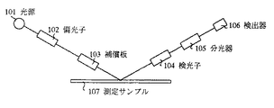
図2は、このようなエリプソメータを使用した光学的膜厚測定の概略を示すものである。同図に示すように、エリプソメータを使用した光学的膜厚測定では、光源101からの光を、偏光状態を調整する偏光子102、位相を調整する補償板103の各光学素子を通過させることによって、楕円偏光状態の入射光を形成し、サンプル107に照射する。
【0004】
そして、サンプル107からの反射光の光路上に、偏光状態を調べるための検光子104、所定波長の光を選択するための分光器105、検出器106を設けて反射光の各波長について偏光状態を測定し、スペクトルを得る。
【0005】
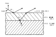
例えば、図3に示すように、Si基板202上に成膜された酸化膜(ゲート酸化膜など)201の膜厚を測定する場合、上記のようにして、空気(屈折率=N0 )200中から角度θ0 で照射された楕円偏光状態の入射光は、酸化膜(屈折率=N1 )201表面で反射するとともに、そのほとんどは酸化膜201内に入射する。そして、酸化膜201内に入射した光は、Si基板202界面(基板面)(屈折率=N2 )で反射して酸化膜201内から空気200中に戻り、酸化膜201表面での反射光と偏光干渉する。
【0006】
上記のような光について、それぞれp偏光成分とs偏光成分を計算し、それぞれの位相差Δと振幅比Ψから膜厚が算出される。
【0007】
Si基板202面での反射光のp偏光成分(r1p)と、s偏光成分(r1s)は、それぞれ以下の式によって計算される。
r1p=(n2 cos θ1 −n1 cos θ2 )/(n2 cos θ1 +n1 cos θ2 )
r1s=(n1 cos θ1 −n2 cos θ2 )/(n1 cos θ1 +n2 cos θ2 )
【0008】
また、検出される光のp偏光成分(RP )とs偏光成分(Rs )は、上記のr1p、r1sと、酸化膜201面での反射光のp偏光成分(r0p)と、s偏光成分 (r0s)から、以下の式により偏光状態が計算される。
RP =(r0p+r1pexp (−2iδ))/(1+r0p・r1pexp (−2iδ))
Rs =(r0s+r1sexp (−2iδ))/(1+r0s・r1sexp (−2iδ))
但し(δ=2πn1 tcos θ1 /λ)
最終的に、
RP /Rs =tan (Ψ)・exp (−iΔ)
を用いて、cos Δとtan Ψを各波長について計算することで、波長依存スペクトルが得られる。そして、酸化膜201の膜厚値tをパラメータとして実測のスペクトルと理論スペクトルを比較することで、膜厚値tが算出できる。
【0009】
また、図4に示すように、Si基板202上に形成された酸化膜201が、グレーティング構造を有する場合、このグレーティング構造の断面形状の測定も、エリプソメータで可能であり、この場合、図5に示すように、パターン部分をL等分に分割し、グレーティング部分をL層の積層膜として形状を求める方法もある。この方法においては、空気とグレーティング構造の誘電率の混合層が存在し、各界面においてn次回折光が発生するというモデルで断面形状を算出している。この場合、図5に示すグレーティングパターンが無限に繰り返される領域を仮定する。グレーティング構造をL層に分割し各層で空気とグレーティング部分の体積比に基づいて誘電率を算出する。そのL層の積層構造にある角度で光を入射したとき、各層の界面において反射と透過のn次回折光が発生するというモデルを立て、それぞれs偏光成分、p偏光成分の振幅反射率を計算する。最終的にcos Δとtan Ψの波長依存性から断面形状を求めることができる。
【0010】
【発明が解決しようとする課題】
上述した膜厚測定方法、断面形状測定方法のいずれも、基板面(下層の反射面)がSi、Al、Cu等の光の吸収係数kが大きい材料(光透過性の低い低光透過性材料)からなり、膜厚が厚く、平坦な非透過性の場合に適用可能である。
【0011】
しかしながら、上述した膜厚測定方法及び断面形状測定方法膜厚では、測定する対象である酸化膜の下層に多層配線構造を有する試料の場合、膜厚測定及び断面形状測定を行うことができないという問題がある。
【0012】
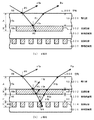
すなわち、例えば、図6に示す試料の場合、図6(a)に示すように、膜厚を測定する対象である酸化膜301からなるa層の下層に、金属配線302と層間絶縁膜303からなるb層、金属配線304と層間絶縁膜305からなるc層が形成され、同図(b)、(c)に示すように、b層の金属配線302とc層の金属配線304とが直交するように形成された多層配線構造を有する。このような多層配線構造のうち、酸化膜301及び層間絶縁膜303,305は、二酸化シリコン等の光透過性の高い高光透過性材料から構成され、金属配線302,304は、Cu、Al、W等の光透過性の低い低光透過性材料から構成されている。なお、図6(a)中、306,307は、SiN膜やSiC膜等からなり、CMP(Chemical Mechanical Polishing )工程で利用されるストッパー層である。
【0013】
また、図7に示す試料の場合、さらに、酸化膜301が、グレーティング構造を有する。
【0014】
上記のような多層配線構造を有する試料の場合、下層の反射面の構造が複雑であるため、理論スペクトルを計算するに当たって、a層の表面とa層とb層の界面とで反射するとして理論スペクトルを計算したり、a層の表面とb層とc層の界面で反射するとして理論スペクトルを計算しても、膜厚測定及び断面形状測定を行うことができなかった。
【0015】
このため、従来においては、多層配線構造上に形成された膜の膜厚測定等を行う場合、製造工程中に、製品ウエハとは別にテストピースウエハを投入し、テストピースウエハ(ベアSi)上に測定対象となる膜を形成し、光学的手法により膜厚測定を行っている。
【0016】
また、エッチング形状の測定の場合についても、テストピースウエハを投入し、成膜、レジスト塗布、露光、エッチングの工程を行って、断面をSEMで観察し、形状の管理を行っている。
【0017】
このため、いずれの場合も、テストピースウエハ数だけ製造コストが増すことになるという問題があった。
【0018】
また、チップ内に膜厚測定あるいはエッチング形状測定のモニタリングパターンを設け、その位置を従来方法で測定することも可能である。しかし、ICの高集積化に伴い、チップ内にある程度の大きさをもったモニタリングパターンを設けることは困難になってきている。また、仮に設けたとしてもパターンが大きいため、CMPの工程処理で、図8に示すように金属配線302の表面がおわん型に削れるディッシングが起こり、金属配線302との界面を反射面として膜厚等を測定する場合、測定精度が悪化するという問題がある。
【0019】
したがって、多層配線上に形成された膜の膜厚及び断面形状を測定、管理するためには、製品ウエハの任意の位置を非破壊、高スループットで測定する方法の開発が求められていた。
【0020】
本発明は、かかる従来の事情に対処してなされたもので、多層配線上に形成された膜の膜厚測定及び断面形状測定を、非破壊かつ高スループットで行うことのできる偏光解析方法及び光学的膜厚測定装置を提供しようとするものである。
【0021】
【課題を解決するための手段】
すなわち、請求項1記載の発明は、測定対象の膜を表面に有する被測定物に所定波長の楕円偏光状態の入射光を所定入射角で照射した時に、前記被測定物から反射する反射光のp偏光成分とs偏光成分の位相差(Δ)に基づく値及び振幅比(Ψ)に基づく値を理論計算により求めて基準データを得るとともに、実際に前記被測定物に前記入射光を照射した時に反射する反射光のp偏光成分とs偏光成分の位相差(Δ)に基づく値及び振幅比(Ψ)に基づく値を測定によって求めて、前記基準データと比較することにより、前記膜の解析を行う偏光解析方法において、前記基準データを得る際に、前記p偏光成分の反射面と、前記s偏光成分の反射面とを異ならせて前記理論計算を行うことを特徴とする。
【0022】
請求項2の発明は、請求項1記載の偏光解析方法において、前記比較は少なくとも2つ以上の波長に基づいてなされることを特徴とする。
【0023】
請求項3の発明は、請求項1記載の偏光解析方法において、前記比較は少なくとも2つ以上の入射角に基づいてなされることを特徴とする。
【0024】
請求項4の発明は、請求項1〜3いずれか1項記載の偏光解析方法において、前記位相差(Δ)に基づく値はcos Δであり、前記振幅比(Ψ)に基づく値はtan Ψであることを特徴とする。
【0025】
請求項5の発明は、請求項1〜4いずれか1項記載の偏光解析方法において、前記被測定物が、最上層に形成され、光透過性の高い高光透過性材料で構成された第1層と、前記第1層の下に設けられ、光透過性の高い高光透過性材料と、光透過性の低い低光透過性材料とで構成される第2の層と、第2の層の下に設けられ、光透過性の高い高光透過性材料で構成される第3層と、前記第3層の下に設けられ、光透過性の低い低光透過性材料からなる基板とを有することを特徴とする。
【0026】
請求項6の発明は、請求項5記載の偏光解析方法において、前記第2層は、前記高光透過性材料と、前記低光透過性材料が、層平面方向に交互に配置された直線状配線構造を有し、前記p偏光成分の偏光面は前記直線状配線と平行であることを特徴とする。
【0027】
請求項7の発明は、請求項6記載の偏光解析方法において、前記基板と前記第3層との間に、光透過性の高い高光透過性材料と、光透過性の低い低光透過性材料が、層平面方向に交互に配置された直線状配線構造を少なくとも表面に有する第4層を有し、前記第4層の直線状配線の方向は、前記第2層の直線状配線の方向と直交する方向であることを特徴とする。
【0028】
請求項8の発明は、請求項7記載の偏光解析方法において、前記s偏光成分は、前記第2層上で反射し、前記p偏光成分は前記第2層を透過し、前記第4層上で反射することを特徴とする。
【0029】
請求項9の発明は、請求項5〜8いずれか1項記載の偏光解析方法において、前記理論計算における前記第2層は、前記p偏光成分に対する屈折率と、前記s偏光成分に対する屈折率とが異なることを特徴とする。
【0030】
請求項10の発明は、請求項5〜9いずれか1項記載の偏光解析方法において、前記光透過性の低い低光透過性材料が金属配線材料であり、前記光透過性の高い高光透過性材料が絶縁性材料であることを特徴とする。
【0031】
請求項11の発明は、請求項1〜10いずれか1項記載の偏光解析方法において、前記測定対象の膜は第1層から第4層の少なくともいずれか1つであって、前記測定対象の膜の膜厚、屈折率、断面形状の少なくともいずれか一つを測定することを特徴とする。
請求項12の発明は、測定対象の膜を表面に有する被測定物に所定波長の楕円偏光状態の入射光を所定入射角で照射した時に、前記被測定物から反射する反射光のp偏光成分とs偏光成分の位相差(Δ)に基づく値及び振幅比(Ψ)に基づく値を理論計算により求めて得られた基準データと、実際に前記被測定物に前記入射光を照射した時に反射する反射光を測定し、当該測定された反射光のp偏光成分とs偏光成分の位相差(Δ)に基づく値及び振幅比(Ψ)に基づく値と、を比較し、前記膜の解析を行う光学的膜厚測定装置において、前記基準データが、前記p偏光成分の反射面と、前記s偏光成分の反射面とを異ならせて前記理論計算を行い求めたものであることを特徴とする。
請求項13の発明は、請求項12記載の光学的膜厚測定装置において、前記比較は少なくとも2つ以上の波長に基づいてなされることを特徴とする。
請求項14の発明は、請求項12記載の光学的膜厚測定装置において、前記比較は少なくとも2つ以上の入射角に基づいてなされることを特徴とする。
請求項15の発明は、請求項12〜14いずれか1項記載の光学的膜厚測定装置において、前記位相差(Δ)に基づく値は cos Δであり、前記振幅比(Ψ)に基づく値は tan Ψであることを特徴とする。
請求項16の発明は、請求項12〜15いずれか1項記載の光学的膜厚測定装置において、前記被測定物が、最上層に形成され、光透過性の高い高光透過性材料で構成された第1層と、前記第1層の下に設けられ、光透過性の高い高光透過性材料と、光透過性の低い低光透過性材料とで構成される第2の層と、第2の層の下に設けられ、光透過性の高い高光透過性材料で構成される第3層と、前記第3層の下に設けられ、光透過性の低い低光透過性材料からなる基板とを有することを特徴とする。
請求項17の発明は、請求項16記載の光学的膜厚測定装置において、前記第2層は、前記高光透過性材料と、前記低光透過性材料が、層平面方向に交互に配置された直線状配線構造を有し、前記p偏光成分の偏光面は前記直線状配線と平行であることを特徴とする。
請求項18の発明は、請求項17記載の光学的膜厚測定装置において、前記基板と前記第3層との間に、光透過性の高い高光透過性材料と、光透過性の低い低光透過性材料が、層平面方向に交互に配置された直線状配線構造を少なくとも表面に有する第4層を有し、前記第4層の直線状配線の方向は、前記第2層の直線状配線の方向と直交する方向であることを特徴とする。
請求項19の発明は、請求項18記載の光学的膜厚測定装置において、前記s偏光成分は、前記第2層上で反射し、前記p偏光成分は前記第2層を透過し、前記第4層上で反射することを特徴とする。
請求項20の発明は、請求項16〜19いずれか1項記載の光学的膜厚測定装置において、前記理論計算における前記第2層は、前記p偏光成分に対する屈折率と、前記s偏光成分に対する屈折率とが異なることを特徴とする。
請求項21の発明は、請求項16〜20いずれか1項記載の光学的膜厚測定装置において、前記光透過性の低い低光透過性材料が金属配線材料であり、前記光透過性の高い高光透過性材料が絶縁性材料であることを特徴とする。
請求項22の発明は、請求項12〜21いずれか1項記載の光学的膜厚測定装置において、前記測定対象の膜は第1層から第4層の少なくともいずれか1つであって、前記測定対象の膜の膜厚、屈折率、断面形状の少なくともいずれか一つを測定することを特徴とする。
【0032】
【発明の実施の形態】
以下、本発明の詳細を、実施の形態について図面を参照して説明する。
【0033】
図1は、前述した図6に示した多層配線構造を有する試料の酸化膜301の膜厚(tA )を測定する場合の例を示すもので、同図では、説明を簡単にするために、図6に示したストッパー層306,307については、図示を省略してある。また、同図において、(a)は、照射された光のうちのs偏光成分の挙動を示しており、(b)は、p偏光成分の挙動を示している。なお、測定に使用されるエリプソメータの構成は、前述した図2に示されるように、光源101、偏光子102、補償板103、検光子104、分光器105、検出器106等から構成されている。
【0034】
図1(a)に示すように、屈折率がN0 の空気300中から、屈折率がNA の酸化膜301からなるA層に照射された入射光のs偏光成分は、その一部が反射角θ0 でA層の表面から反射され(r0s)、残りがA層内に入射する。
【0035】
そして、A層内に入射したs偏光成分は、A層を通過して、金属配線302と層間絶縁膜303からなるB層との界面に到達するが、s偏光成分は、金属配線302の配線方向(配線の長手方向)と垂直な方向に振幅しているため、B層の金属配線302間に形成された層間絶縁膜303形成領域を通過することができず、B層との界面において反射角θ1 で反射される。この反射光の振幅反射率r1sは、
r1s=(NA cos θ1 −NBscos θ2 )/(NA cos θ1 +NBscos θ2 )
で表せる。なお、NBsは、B層のs偏光成分に対する屈折率である。
【0036】
この反射光(r1s)が、B層を通過し、A層表面で反射した反射光(r0s)と干渉するが、その干渉光の振幅反射率Rs は、
Rs =(r0s+r1sexp (−2iδ))/(1+r0s・r1sexp (−2iδ))
但し、
δ=2πNA tA cos θ1 /λ
r0s=(N0 cos θ0 −NA cos θ1 )/(N0 cos θ0 +NA cos θ1 )
である。
【0037】
一方、図1(b)は、照射された光のうち、p偏光成分の挙動を示している。屈折率がN0 の空気300中から、屈折率がNA の酸化膜301からなるA層に照射された入射光のp偏光成分は、その一部が反射角θ0 でA層の表面から反射され(r0p)、残りがA層内に入射する。
【0038】
そして、A層内に入射したp偏光成分は、A層を通過して、金属配線302と層間絶縁膜303からなるB層との界面に到達するが、p偏光成分は、金属配線302の配線方向(配線の長手方向)と平行な方向に振幅しているため、B層の金属配線302間に形成された層間絶縁膜303形成領域を通過することができる。そして、この通過したp偏光成分は、さらに、層間絶縁膜303のみからなるC層を通過して、金属配線304と層間絶縁膜305からなるD層との界面に到達する。なお、同図に示されるとおり、B層との界面、C層との界面において、一部のp偏光成分は、反射角θ1 ,θ2 で反射される。
【0039】
D層の金属配線304は、p偏光成分の振幅方向に対して垂直であるので、p偏光成分は、D層の金属配線304間に形成された層間絶縁膜305形成領域を通過することができず、D層との界面に到達したp偏光成分は、ここで、反射角θ3 で反射される。この反射光の振幅反射率r3Pは、
r3P=(ND cos θ3 −NC cos θ4 )/(ND cos θ3 +NC cos θ4 )
で表せる。
【0040】
s偏光成分に対するB層と、p偏光成分に対するD層は、実質的に基板面(非透過面)のように作用しているので、s偏光成分に対するB層の屈折率NBsと、p偏光成分に対するD層の屈折率ND との間には、ND =NBsが成立する。但し、B層とC層の金属配線の線幅及び間隔が等しい場合に限る。
【0041】
D層との界面で反射した反射光(r3p)は、C層を通過し、C層との界面で反射した反射光(r2p)と干渉するが、この干渉光の振幅反射率R2pは、
R2p=(r2p+r3pexp (−2iδ))/(1+r2p・r3pexp (−2iδ))
但し、
δ=2πNC tCcosθ3 /λ
r2p=(NC cos θ2 −NBpcos θ3 )/(NC cos θ2 +NBpcos θ3 )
である。
【0042】
ここで、B層について説明すると、既にs偏光成分の計算において、B層の屈折率をNBsと定義したが、B層は膜厚により屈折率が変化するCu、W、Al等の金属を含む層である。このような層の場合、s偏光成分に対して基板面(非透過面)のように機能する場合と、p偏光成分に対して透過膜として機能する場合の屈折率は異なり、NBs≠NBpである。
【0043】
前述した干渉光(R2p)がB層を通過する場合も同様に考えると、B層での振幅反射率R1pは、
R1p=(r1p+R2pexp (−2iδ))/(1+r1p・R2pexp (−2iδ))
但し、
δ=2πNBptB cos θ2 /λ
r1p=(NBpcos θ1 −NA cos θ2 )/(NBpcos θ1 +NA cos θ2 )
である。最終的に、A層表面での振幅反射率Rp は、
Rp =(r0p+R1pexp (−2iδ))/(1+r0p・R1pexp (−2iδ))
但し、
δ=2πNA tA cos θ1 /λ
r0p=(NA cos θ0 −N0 cos θ1 )/(NA cos θ0 +N0 cos θ1 )
となる。
【0044】
以上のようにして、基板面(非透過面)のように作用する反射面を、s偏光成分とp偏光成分でそれぞれ分けて計算した振幅反射率Rs ,Rp から、s偏光成分とp偏光成分の振幅比Ψと位相差Δの関数であるtan Ψとcos Δが、以下の式から計算できる。
Rs /Rp =tan Ψ・exp (−iΔ)
【0045】
以上は、任意の波長λについて説明したもので、連続する複数の波長について、tan Ψとcos Δを計算することで、基準データとなるλ−tan Ψとλ−cos Δのスペクトルデータが得られる。
【0046】
そして、異なるA層の膜厚tA に関してこのように求められた基準データのスペクトルデータと、実際に測定して得られた実測のスペクトルデータとを、膜厚及び膜質に関するパラメータを振って比較し、その誤差を示す統計量が最小あるいは最大となる膜厚を出力値とする方法で、多層配線上に形成された酸化膜301(A層)の膜厚を測定することができる。
【0047】
なお試料が90°回転した状態で、s偏光成分とp偏光成分の反射・透過が逆になるパターンでもよい。
【0048】
また、上述したように、s偏光成分とp偏光成分が、それぞれ異なる面で反射するとして、tan Ψとcos Δの波長依存性を計算し、実測スペクトルと比較する方法は、図7に示したように、グレーティング構造のエッチング形状測定等の断面形状測定にも適用可能である。最上層に形成された断面形状算出に関しては、図5に示したようにパターン部分をn等分に分割し、グレーティング部分をn層の積層膜として形状を求める方法を使用する。
【0049】
さらに、上記の実施形態では、B層とD層に、互いに直交する金属配線302,304が形成されている場合について説明したが、下層のD層については、金属配線304ではなく、基板面等の非透過面で構成されているものでも、同様にして適用することができる。
【0050】
さらにまた、波長の代わりに入射角を可変とすることで同様の効果が得られる。例えば図1において入射角θ0 を可変にして測定を行うことでcos Δとtan Ψの入射角依存性が得られる。そして前記した式に基づき複数の入射角で計算することでθ−cos Δとθ−tan Ψの基準データが得られる。基準データと実測のスペクトルデータを比較することで所望の膜厚及び断面形状に関する物理量を求めることが可能である。
【0051】
【発明の効果】
以上説明したとおり、本発明によれば、多層配線上に形成された膜の膜厚測定及び断面形状測定を、非破壊かつ高スループットで行うことができる。
【図面の簡単な説明】
【図1】本発明の測定法の一実施形態を説明するための図。
【図2】本発明方法に使用するエリプソメータの概略構成を示す図。
【図3】従来の膜厚測定方法を説明するための基板断面の概略構成を示す図。
【図4】従来の断面形状測定方法を説明するための基板断面の概略構成を示す図。
【図5】従来の断面形状測定方法を説明するための基板断面の概略構成を示す図。
【図6】従来技術の問題点を説明するための基板断面の概略構成を示す図。
【図7】従来技術の問題点を説明するための基板断面の概略構成を示す図。
【図8】従来技術の問題点を説明するための基板断面の概略構成を示す図。
【符号の説明】
300……空気、301……熱酸化膜、302,304……金属配線、303,305……層間絶縁膜。[0001]
BACKGROUND OF THE INVENTION
The present invention relates to a polarization analysis method and an optical film thickness measurement device , and more particularly to a polarization analysis method and an optical film thickness measurement device suitable for film thickness measurement in a manufacturing process of a semiconductor device and measurement of a cross-sectional shape such as an etching shape. About.
[0002]
[Prior art]
Conventionally, optical film thickness measurement using an ellipsometer has been used in, for example, a film thickness inspection process in a semiconductor device manufacturing process.
[0003]
FIG. 2 shows an outline of optical film thickness measurement using such an ellipsometer. As shown in the figure, in the optical film thickness measurement using an ellipsometer, the light from the light source 101 is passed through the optical elements of the polarizer 102 for adjusting the polarization state and the compensation plate 103 for adjusting the phase. Then, incident light in an elliptically polarized state is formed and irradiated to the sample 107.
[0004]
Then, an
[0005]
For example, as shown in FIG. 3, when the film thickness of an oxide film (gate oxide film or the like) 201 formed on the
[0006]
For the light as described above, the p-polarized component and the s-polarized component are calculated, and the film thickness is calculated from the phase difference Δ and the amplitude ratio Ψ.
[0007]
The p-polarized component (r 1p ) and the s-polarized component (r 1s ) of the reflected light on the
r 1p = (n 2 cos θ 1 −n 1 cos θ 2 ) / (n 2 cos θ 1 + n 1 cos θ 2 )
r 1s = (n 1 cos θ 1 −n 2 cos θ 2 ) / (n 1 cos θ 1 + n 2 cos θ 2 )
[0008]
In addition, the p-polarized component (R P ) and the s-polarized component (R s ) of the detected light are the above-mentioned r 1p and r 1s and the p-polarized component (r 0p ) of the reflected light on the oxide film 201 surface. , The polarization state is calculated from the s-polarization component (r 0s ) according to the following equation.
R P = (r 0p + r 1p exp (−2iδ)) / (1 + r 0p · r 1p exp (−2iδ))
R s = (r 0s + r 1s exp (−2iδ)) / (1 + r 0s · r 1s exp (−2iδ))
However, (δ = 2πn 1 tcos θ 1 / λ)
Finally,
R P / R s = tan (Ψ) · exp (−iΔ)
A wavelength dependent spectrum is obtained by calculating cos Δ and tan Ψ for each wavelength using. The film thickness value t can be calculated by comparing the measured spectrum with the theoretical spectrum using the film thickness value t of the oxide film 201 as a parameter.
[0009]
As shown in FIG. 4, when the oxide film 201 formed on the
[0010]
[Problems to be solved by the invention]
In both the film thickness measuring method and the cross-sectional shape measuring method described above, the substrate surface (lower reflective surface) is a material having a large light absorption coefficient k such as Si, Al, Cu, etc. (low light transmissive material having low light transmittance) It is applicable when the film thickness is thick and flat and impermeable.
[0011]
However, with the film thickness measurement method and the cross-sectional shape measurement method described above, the film thickness measurement and the cross-sectional shape measurement cannot be performed in the case of a sample having a multilayer wiring structure under the oxide film to be measured. There is.
[0012]
That is, for example, in the case of the sample shown in FIG. 6, as shown in FIG. 6A, the metal wiring 302 and the interlayer insulating film 303 are formed below the a layer made of the
[0013]
Further, in the case of the sample shown in FIG. 7, the
[0014]
In the case of the sample having the multilayer wiring structure as described above, since the structure of the lower reflective surface is complicated, it is assumed that when the theoretical spectrum is calculated, it is reflected at the surface of the a layer and the interface between the a layer and the b layer. Even if the spectrum was calculated or the theoretical spectrum was calculated assuming that the light was reflected at the surface of the a layer and the interface between the b layer and the c layer, the film thickness measurement and the cross-sectional shape measurement could not be performed.
[0015]
For this reason, conventionally, when measuring the film thickness of a film formed on a multilayer wiring structure, a test piece wafer is introduced separately from the product wafer during the manufacturing process, and the test piece wafer (bare Si) is placed on the test piece wafer (bare Si). A film to be measured is formed on the film, and the film thickness is measured by an optical method.
[0016]
Also in the case of measuring the etching shape, a test piece wafer is loaded, film forming, resist coating, exposure, and etching processes are performed, and the cross section is observed with an SEM to manage the shape.
[0017]
For this reason, in either case, there is a problem that the manufacturing cost is increased by the number of test piece wafers.
[0018]
It is also possible to provide a monitoring pattern for film thickness measurement or etching shape measurement in the chip and measure the position by a conventional method. However, with the high integration of ICs, it has become difficult to provide a monitoring pattern having a certain size in a chip. Further, even if provided, since the pattern is large, dishing occurs in the CMP process so that the surface of the metal wiring 302 is cut into a bowl shape as shown in FIG. 8, and the film thickness is obtained with the interface with the metal wiring 302 as a reflective surface. Etc., there is a problem that measurement accuracy deteriorates.
[0019]
Therefore, in order to measure and manage the film thickness and cross-sectional shape of the film formed on the multilayer wiring, development of a method for measuring an arbitrary position of the product wafer with non-destructive and high throughput has been demanded.
[0020]
The present invention has been made in response to such a conventional situation, and a polarization analysis method and an optical device capable of performing non-destructive and high-throughput measurement of film thickness and cross-sectional shape of a film formed on a multilayer wiring. An objective film thickness measuring device is to be provided.
[0021]
[Means for Solving the Problems]
That is, according to the first aspect of the present invention, the reflected light reflected from the object to be measured is irradiated when the object to be measured having the film to be measured on the surface is irradiated with the incident light having the elliptical polarization state with the predetermined wavelength at the predetermined incident angle. A value based on the phase difference (Δ) between the p-polarized component and the s-polarized component and a value based on the amplitude ratio (Ψ) are obtained by theoretical calculation to obtain reference data, and the incident light is actually irradiated on the object to be measured. Analyzing the film by obtaining a value based on the phase difference (Δ) and a value based on the amplitude ratio (Ψ) of the p-polarized component and the s-polarized component of the reflected light that is sometimes reflected and comparing it with the reference data In the polarization analysis method for performing the above, when the reference data is obtained, the theoretical calculation is performed by making the reflective surface of the p-polarized component different from the reflective surface of the s-polarized component.
[0022]
According to a second aspect of the present invention, in the ellipsometry method according to the first aspect, the comparison is made based on at least two or more wavelengths.
[0023]
According to a third aspect of the present invention, in the ellipsometry method according to the first aspect, the comparison is made based on at least two incident angles.
[0024]
The invention according to claim 4 is the ellipsometry method according to any one of
[0025]
According to a fifth aspect of the present invention, in the ellipsometry method according to any one of the first to fourth aspects, the object to be measured is the first layer formed on the uppermost layer and made of a highly light transmissive material having a high light transmittance. A second layer composed of a layer, a high light-transmitting material having a high light-transmitting property, and a low light-transmitting material having a low light-transmitting property, and a second layer formed below the first layer, A third layer made of a high light-transmitting material having a high light-transmitting property and a substrate made of a low light-transmitting material having a low light-transmitting property provided under the third layer; It is characterized by.
[0026]
A sixth aspect of the present invention is the ellipsometry method according to the fifth aspect, wherein the second layer has a linear wiring in which the high light transmissive material and the low light transmissive material are alternately arranged in the layer plane direction. And a polarization plane of the p-polarized light component is parallel to the linear wiring.
[0027]
A seventh aspect of the present invention is the ellipsometric method according to the sixth aspect, wherein a high light transmissive material having a high light transmittance and a low light transmissive material having a low light transmittance are provided between the substrate and the third layer. Has a fourth layer having at least a surface of a linear wiring structure arranged alternately in the layer plane direction, and the direction of the linear wiring of the fourth layer is the direction of the linear wiring of the second layer. It is characterized by orthogonal directions.
[0028]
The invention of claim 8 is the ellipsometry method according to claim 7, wherein the s-polarized component is reflected on the second layer, the p-polarized component is transmitted through the second layer, and on the fourth layer. It is reflected by.
[0029]
The invention of claim 9 is the polarization analysis method according to any one of claims 5 to 8, wherein the second layer in the theoretical calculation includes a refractive index for the p-polarized component and a refractive index for the s-polarized component. Are different.
[0030]
A tenth aspect of the present invention is the ellipsometric analysis method according to any one of the fifth to ninth aspects, wherein the low light transmissive material having low light transmittance is a metal wiring material, and the light transmittance is high. The material is an insulating material.
[0031]
The eleventh aspect of the present invention is the ellipsometry method according to any one of the first to tenth aspects, wherein the film to be measured is at least one of a first layer to a fourth layer, At least one of the film thickness, refractive index, and cross-sectional shape of the film is measured.
The invention according to claim 12 is the p-polarized component of the reflected light reflected from the object to be measured when the object to be measured having the film to be measured is irradiated with the incident light in the elliptically polarized state having the predetermined wavelength at the predetermined incident angle. And reference data obtained by theoretical calculation of a value based on the phase difference (Δ) of the s-polarized component and a value based on the amplitude ratio (Ψ), and reflection when the incident light is actually irradiated onto the object to be measured The reflected light is measured, and the value based on the phase difference (Δ) and the value based on the amplitude ratio (Ψ) of the p-polarized component and the s-polarized component of the measured reflected light are compared to analyze the film. In the optical film thickness measurement apparatus to be performed, the reference data is obtained by performing the theoretical calculation by differentiating the reflection surface of the p-polarized component and the reflection surface of the s-polarized component. .
According to a thirteenth aspect of the present invention, in the optical film thickness measuring apparatus according to the twelfth aspect, the comparison is made based on at least two wavelengths.
According to a fourteenth aspect of the present invention, in the optical film thickness measuring apparatus according to the twelfth aspect, the comparison is made based on at least two incident angles.
The invention according to claim 15 is the optical film thickness measuring device according to any one of claims 12 to 14, wherein the value based on the phase difference (Δ) is cos Δ and the value based on the amplitude ratio (Ψ). Is characterized by tan Ψ.
According to a sixteenth aspect of the present invention, in the optical film thickness measuring device according to any one of the twelfth to fifteenth aspects, the object to be measured is formed of an uppermost layer and is made of a highly light transmissive material having a high light transmittance. A first layer, a second layer that is provided under the first layer, and includes a high light-transmitting material having a high light-transmitting property and a low light-transmitting material having a low light-transmitting property; A third layer made of a high light-transmitting material having a high light-transmitting property and a substrate made of a low light-transmitting material having a low light-transmitting property provided under the third layer; It is characterized by having.
According to a seventeenth aspect of the present invention, in the optical film thickness measuring apparatus according to the sixteenth aspect, the second layer has the high light transmissive material and the low light transmissive material alternately arranged in a layer plane direction. It has a linear wiring structure, and the polarization plane of the p-polarized light component is parallel to the linear wiring.
According to an eighteenth aspect of the present invention, in the optical film thickness measuring apparatus according to the seventeenth aspect, between the substrate and the third layer, a highly light transmissive material having a high light transmittance and a low light having a low light transmittance. The transparent material has at least a fourth layer having a linear wiring structure arranged alternately in the layer plane direction on the surface, and the direction of the linear wiring of the fourth layer is the linear wiring of the second layer It is a direction orthogonal to the direction of.
According to a nineteenth aspect of the present invention, in the optical film thickness measuring device according to the eighteenth aspect, the s-polarized component is reflected on the second layer, the p-polarized component is transmitted through the second layer, and the first It is characterized by reflecting on four layers.
The invention according to claim 20 is the optical film thickness measuring device according to any one of claims 16 to 19, wherein the second layer in the theoretical calculation has a refractive index with respect to the p-polarized component and with respect to the s-polarized component. The refractive index is different.
The invention according to claim 21 is the optical film thickness measuring device according to any one of claims 16 to 20, wherein the low light-transmitting material having low light transmittance is a metal wiring material, and the light transmitting property is high. The high light-transmitting material is an insulating material.
The invention of claim 22 is the optical film thickness measuring device according to any one of claims 12 to 21, wherein the film to be measured is at least one of a first layer to a fourth layer, It is characterized by measuring at least one of the film thickness, refractive index, and cross-sectional shape of the film to be measured.
[0032]
DETAILED DESCRIPTION OF THE INVENTION
The details of the present invention will be described below with reference to the drawings.
[0033]
FIG. 1 shows an example in the case of measuring the thickness (tA) of the
[0034]
As shown in FIG. 1A, a part of the s-polarized light component of the incident light irradiated from the
[0035]
The s-polarized component incident on the A layer passes through the A layer and reaches the interface between the metal wiring 302 and the B layer formed of the interlayer insulating film 303, but the s-polarized component is the wiring of the metal wiring 302. Since the amplitude is in the direction perpendicular to the direction (longitudinal direction of the wiring), it cannot pass through the formation region of the interlayer insulating film 303 formed between the metal wirings 302 of the B layer and is reflected at the interface with the B layer. Reflected at angle θ1. The amplitude reflectance r1s of this reflected light is
r1s = (NA cos θ1−NBscos θ2) / (NA cos θ1 + NBscos θ2)
It can be expressed as Note that NBs is the refractive index for the s-polarized component of the B layer.
[0036]
The reflected light (r1s) passes through the B layer and interferes with the reflected light (r0s) reflected on the surface of the A layer. The amplitude reflectance Rs of the interference light is
Rs = (r0s + r1sexp (-2i.delta.)) / (1 + r0s.r1sexp (-2i.delta.))
However,
δ = 2πNA tA cos θ1 / λ
r0s = (N0 cos θ0−NA cos θ1) / (N0 cos θ0 + NA cos θ1)
It is.
[0037]
On the other hand, FIG. 1B shows the behavior of the p-polarized component in the irradiated light. Part of the p-polarized component of incident light irradiated from the
[0038]
The p-polarized component incident on the A layer passes through the A layer and reaches the interface between the metal wiring 302 and the B layer formed of the interlayer insulating film 303, but the p-polarized component is the wiring of the metal wiring 302. Since the amplitude is in a direction parallel to the direction (longitudinal direction of the wiring), it can pass through the formation region of the interlayer insulating film 303 formed between the metal wirings 302 of the B layer. Then, the p-polarized component that has passed through further passes through the C layer made up of only the interlayer insulating film 303 and reaches the interface between the
[0039]
Since the
r3P = (ND cos θ3−NC cos θ4) / (ND cos θ3 + NC cos θ4)
It can be expressed as
[0040]
Since the B layer for the s-polarized component and the D layer for the p-polarized component act substantially like a substrate surface (non-transparent surface), the refractive index NBs of the B layer for the s-polarized component and the p-polarized component ND = NBs holds between the refractive index ND of the D layer and ND. However, this is limited to the case where the line widths and intervals of the metal wirings of the B layer and the C layer are equal.
[0041]
The reflected light (r3p) reflected at the interface with the D layer passes through the C layer and interferes with the reflected light (r2p) reflected at the interface with the C layer. The amplitude reflectance R2p of this interference light is
R2p = (r2p + r3pexp (-2i.delta.)) / (1 + r2p.r3pexp (-2i.delta.))
However,
δ = 2πNC tCcosθ3 / λ
r2p = (NC cos .theta.2 -NBpcos .theta.3) / (NC cos .theta.2 + NBpcos .theta.3)
It is.
[0042]
Here, the B layer will be described. In the calculation of the s-polarized light component, the refractive index of the B layer is already defined as NBs. However, the B layer contains a metal such as Cu, W, or Al whose refractive index changes depending on the film thickness. Is a layer. In the case of such a layer, the refractive index when the s-polarized component functions as a substrate surface (non-transmissive surface) and when the p-polarized component functions as a transmissive film are different, and NBs ≠ NBp. is there.
[0043]
Similarly, when the interference light (R2p) passes through the B layer, the amplitude reflectance R1p in the B layer is
R1p = (r1p + R2pexp (-2i.delta.)) / (1 + r1p.R2pexp (-2i.delta.))
However,
δ = 2πNBptB cos θ2 / λ
r1p = (NBpcos θ1-NA cos θ2) / (NBpcos θ1 + NA cos θ2)
It is. Finally, the amplitude reflectivity Rp on the surface of layer A is
Rp = (r0p + R1pexp (-2i.delta.)) / (1 + r0p.R1pexp (-2i.delta.))
However,
δ = 2πNA tA cos θ1 / λ
r0p = (NA cos .theta.0 -N0 cos .theta.1) / (NA cos .theta.0 + N0 cos .theta.1)
It becomes.
[0044]
As described above, the reflection surface acting as a substrate surface (non-transmission surface) is divided into the s-polarized component and the p-polarized component, and the s-polarized component and the p-polarized component are calculated from the amplitude reflectances Rs and Rp. Tan Ψ and cos Δ, which are functions of the amplitude ratio Ψ and the phase difference Δ, can be calculated from the following equations.
Rs / Rp = tan .PSI.exp (-i.DELTA.)
[0045]
The above is an explanation of an arbitrary wavelength λ. By calculating tan Ψ and cos Δ for a plurality of continuous wavelengths, spectral data of λ-tan Ψ and λ-cos Δ as reference data can be obtained. .
[0046]
Then, the spectral data of the reference data thus obtained with respect to the film thickness tA of the different A layers and the actually measured spectral data obtained by actual measurement are compared by changing parameters relating to the film thickness and film quality, The film thickness of the oxide film 301 (A layer) formed on the multilayer wiring can be measured by a method in which the film thickness at which the statistic indicating the error is minimum or maximum is used as the output value.
[0047]
A pattern in which the reflection and transmission of the s-polarized component and the p-polarized component are reversed when the sample is rotated by 90 ° may be used.
[0048]
Further, as described above, the method of calculating the wavelength dependence of tan Ψ and cos Δ and comparing with the measured spectrum, assuming that the s-polarized component and the p-polarized component are reflected by different surfaces, is shown in FIG. Thus, the present invention can also be applied to cross-sectional shape measurement such as etching shape measurement of a grating structure. As for the calculation of the cross-sectional shape formed in the uppermost layer, as shown in FIG. 5, a method is used in which the pattern portion is divided into n equal parts and the shape is obtained by using the grating portion as a laminated film of n layers.
[0049]
Further, in the above-described embodiment, the case where the
[0050]
Furthermore, the same effect can be obtained by making the incident angle variable instead of the wavelength. For example, in FIG. 1, the incident angle dependence of cos Δ and tan ψ can be obtained by making the
[0051]
【The invention's effect】
As described above, according to the present invention, the film thickness measurement and the cross-sectional shape measurement of the film formed on the multilayer wiring can be performed nondestructively and with high throughput.
[Brief description of the drawings]
FIG. 1 is a diagram for explaining one embodiment of a measurement method of the present invention.
FIG. 2 is a diagram showing a schematic configuration of an ellipsometer used in the method of the present invention.
FIG. 3 is a diagram showing a schematic configuration of a substrate cross section for explaining a conventional film thickness measuring method.
FIG. 4 is a diagram showing a schematic configuration of a cross-section of a substrate for explaining a conventional cross-sectional shape measuring method.
FIG. 5 is a diagram showing a schematic configuration of a cross-section of a substrate for explaining a conventional cross-sectional shape measuring method.
FIG. 6 is a diagram showing a schematic configuration of a cross section of a substrate for explaining problems of the prior art.
FIG. 7 is a diagram showing a schematic configuration of a cross section of a substrate for explaining problems of the prior art.
FIG. 8 is a diagram showing a schematic configuration of a cross section of a substrate for explaining problems of the prior art.
[Explanation of symbols]
300 ... Air, 301 ... Thermal oxide film, 302,304 ... Metal wiring, 303,305 ... Interlayer insulating film.
Claims (22)
実際に前記被測定物に前記入射光を照射した時に反射する反射光のp偏光成分とs偏光成分の位相差(Δ)に基づく値及び振幅比(Ψ)に基づく値を測定によって求めて、前記基準データと比較することにより、前記膜の解析を行う偏光解析方法において、
前記基準データを得る際に、前記p偏光成分の反射面と、前記s偏光成分の反射面とを異ならせて前記理論計算を行うことを特徴とする偏光解析方法。The phase difference between the p-polarized component and the s-polarized component of the reflected light reflected from the object to be measured when the object to be measured having the film to be measured is irradiated with the elliptically polarized light having a predetermined wavelength at a predetermined incident angle. While obtaining a value based on (Δ) and a value based on the amplitude ratio (Ψ) by theoretical calculation to obtain reference data,
The value based on the phase difference (Δ) and the value based on the amplitude ratio (ψ) of the p-polarized component and the s-polarized component of the reflected light that is reflected when the incident light is actually irradiated onto the object to be measured are obtained by measurement, In the polarization analysis method for analyzing the film by comparing with the reference data,
A polarization analysis method characterized in that, when obtaining the reference data, the theoretical calculation is performed by making the reflection surface of the p-polarized component different from the reflection surface of the s-polarized component.
前記比較は少なくとも2つ以上の波長に基づいてなされることを特徴とする偏光解析方法。The ellipsometry method according to claim 1,
The polarization analysis method characterized in that the comparison is made based on at least two wavelengths.
前記比較は少なくとも2つ以上の入射角に基づいてなされることを特徴とする偏光解析方法。The ellipsometry method according to claim 1,
The comparison method is characterized in that the comparison is made based on at least two incident angles.
前記位相差(Δ)に基づく値はcos Δであり、前記振幅比(Ψ)に基づく値はtan Ψであることを特徴とする偏光解析方法。In the polarization analysis method according to any one of claims 1 to 3,
A polarization analysis method characterized in that a value based on the phase difference (Δ) is cos Δ and a value based on the amplitude ratio (ψ) is tan ψ.
前記被測定物が、
最上層に形成され、光透過性の高い高光透過性材料で構成された第1層と、
前記第1層の下に設けられ、光透過性の高い高光透過性材料と、光透過性の低い低光透過性材料とで構成される第2の層と、
第2の層の下に設けられ、光透過性の高い高光透過性材料で構成される第3層と、
前記第3層の下に設けられ、光透過性の低い低光透過性材料からなる基板と
を有することを特徴とする偏光解析方法。In the ellipsometric analysis method according to any one of claims 1 to 4,
The object to be measured is
A first layer formed of a highly light-transmitting material having a high light-transmitting property formed in the uppermost layer;
A second layer that is provided under the first layer and is composed of a high light-transmitting material having a high light-transmitting property and a low light-transmitting material having a low light-transmitting property;
A third layer that is provided under the second layer and is made of a highly light transmissive material having high light transmittance;
And a substrate made of a low-light-transmitting material having a low light-transmitting property provided under the third layer.
前記第2層は、前記高光透過性材料と、前記低光透過性材料が、層平面方向に交互に配置された直線状配線構造を有し、
前記p偏光成分の偏光面は前記直線状配線と平行であることを特徴とする偏光解析方法。In the ellipsometry method according to claim 5,
The second layer has a linear wiring structure in which the high light transmissive material and the low light transmissive material are alternately arranged in a layer plane direction,
A polarization analysis method, wherein a polarization plane of the p-polarized light component is parallel to the linear wiring.
前記基板と前記第3層との間に、光透過性の高い高光透過性材料と、光透過性の低い低光透過性材料が、層平面方向に交互に配置された直線状配線構造を少なくとも表面に有する第4層を有し、
前記第4層の直線状配線の方向は、前記第2層の直線状配線の方向と直交する方向であることを特徴とする偏光解析方法。The ellipsometry method according to claim 6,
At least a linear wiring structure in which a high light-transmitting material with high light transmission and a low light-transmitting material with low light transmission are alternately arranged in the layer plane direction between the substrate and the third layer. Having a fourth layer on the surface;
The direction of the linear wiring of the fourth layer is a direction orthogonal to the direction of the linear wiring of the second layer.
前記s偏光成分は、前記第2層上で反射し、前記p偏光成分は前記第2層を透過し、前記第4層上で反射することを特徴とする偏光解析方法。In the ellipsometry method according to claim 7,
The polarization analysis method, wherein the s-polarized component is reflected on the second layer, and the p-polarized component is transmitted through the second layer and reflected on the fourth layer.
前記理論計算における前記第2層は、前記p偏光成分に対する屈折率と、前記s偏光成分に対する屈折率とが異なることを特徴とする偏光解析方法。In the ellipsometry method according to any one of claims 5 to 8,
The second layer in the theoretical calculation has a refractive index for the p-polarized component and a refractive index for the s-polarized component different from each other.
前記光透過性の低い低光透過性材料が金属配線材料であり、前記光透過性の高い高光透過性材料が絶縁性材料であることを特徴とする偏光解析方法。In the ellipsometry method according to any one of claims 5 to 9,
The polarization analysis method, wherein the low light-transmitting material having low light transmittance is a metal wiring material, and the high light-transmitting material having high light transmittance is an insulating material.
前記測定対象の膜は第1層から第4層の少なくともいずれか1つであって、前記測定対象の膜の膜厚、屈折率、断面形状の少なくともいずれか一つを測定することを特徴とする偏光解析方法。In the ellipsometry method according to any one of claims 1 to 10,
The film to be measured is at least one of a first layer to a fourth layer, and at least one of a film thickness, a refractive index, and a cross-sectional shape of the film to be measured is measured. Ellipsometric analysis method.
実際に前記被測定物に前記入射光を照射した時に反射する反射光を測定し、当該測定された反射光のp偏光成分とs偏光成分の位相差(Δ)に基づく値及び振幅比(Ψ)に基づく値と、
を比較し、前記膜の解析を行う光学的膜厚測定装置において、
前記基準データが、前記p偏光成分の反射面と、前記s偏光成分の反射面とを異ならせて前記理論計算を行い求めたものであることを特徴とする光学的膜厚測定装置。The phase difference between the p-polarized component and the s-polarized component of the reflected light reflected from the object to be measured when the object to be measured having the film to be measured is irradiated with the elliptically polarized light having a predetermined wavelength at a predetermined incident angle. Reference data obtained by calculating a value based on (Δ) and a value based on the amplitude ratio (Ψ) by theoretical calculation;
The reflected light reflected when the incident light is actually irradiated onto the object to be measured is measured, and the value and amplitude ratio (Ψ based on the phase difference (Δ) between the p-polarized component and the s-polarized component of the measured reflected light. ) Based on
In the optical film thickness measuring device for analyzing the film,
The optical film thickness measuring apparatus according to claim 1, wherein the reference data is obtained by performing the theoretical calculation by differentiating a reflection surface of the p-polarized component and a reflection surface of the s-polarized component.
前記比較は少なくとも2つ以上の波長に基づいてなされることを特徴とする光学的膜厚測定装置。In the optical film thickness measuring device according to claim 12,
The comparison is made based on at least two or more wavelengths.
前記比較は少なくとも2つ以上の入射角に基づいてなされることを特徴とする光学的膜厚測定装置。In the optical film thickness measuring device according to claim 12,
The comparison is performed based on at least two incident angles.
前記位相差(Δ)に基づく値はcos Δであり、前記振幅比(Ψ)に基づく値はtan Ψであることを特徴とする光学的膜厚測定装置。In the optical film thickness measuring device according to any one of claims 12 to 14,
A value based on the phase difference (Δ) is cos Δ, and a value based on the amplitude ratio (ψ) is tan ψ.
前記被測定物が、
最上層に形成され、光透過性の高い高光透過性材料で構成された第1層と、
前記第1層の下に設けられ、光透過性の高い高光透過性材料と、光透過性の低い低光透過性材料とで構成される第2の層と、
第2の層の下に設けられ、光透過性の高い高光透過性材料で構成される第3層と、
前記第3層の下に設けられ、光透過性の低い低光透過性材料からなる基板と
を有することを特徴とする光学的膜厚測定装置。In the optical film thickness measuring device according to any one of claims 12 to 15,
The object to be measured is
A first layer formed of a highly light-transmitting material having a high light-transmitting property formed in the uppermost layer;
A second layer that is provided under the first layer and is composed of a high light-transmitting material having a high light-transmitting property and a low light-transmitting material having a low light-transmitting property;
A third layer that is provided under the second layer and is made of a highly light transmissive material having high light transmittance;
An optical film thickness measuring apparatus comprising: a substrate made of a low light transmitting material having a low light transmitting property provided under the third layer.
前記第2層は、前記高光透過性材料と、前記低光透過性材料が、層平面方向に交互に配置された直線状配線構造を有し、
前記p偏光成分の偏光面は前記直線状配線と平行であることを特徴とする光学的膜厚測定装置。The optical film thickness measuring device according to claim 16,
The second layer has a linear wiring structure in which the high light transmissive material and the low light transmissive material are alternately arranged in a layer plane direction,
An optical film thickness measuring apparatus, wherein a polarization plane of the p-polarized light component is parallel to the linear wiring.
前記基板と前記第3層との間に、光透過性の高い高光透過性材料と、光透過性の低い低光透過性材料が、層平面方向に交互に配置された直線状配線構造を少なくとも表面に有する第4層を有し、
前記第4層の直線状配線の方向は、前記第2層の直線状配線の方向と直交する方向であることを特徴とする光学的膜厚測定装置。The optical film thickness measuring device according to claim 17,
At least a linear wiring structure in which a high light-transmitting material with high light transmission and a low light-transmitting material with low light transmission are alternately arranged in the layer plane direction between the substrate and the third layer. Having a fourth layer on the surface;
The optical film thickness measuring apparatus according to claim 4, wherein the direction of the fourth layer linear wiring is perpendicular to the direction of the second layer linear wiring.
前記s偏光成分は、前記第2層上で反射し、前記p偏光成分は前記第2層を透過し、前記第4層上で反射することを特徴とする光学的膜厚測定装置。The optical film thickness measuring device according to claim 18,
The optical film thickness measuring apparatus, wherein the s-polarized component is reflected on the second layer, and the p-polarized component is transmitted through the second layer and reflected on the fourth layer.
前記理論計算における前記第2層は、前記p偏光成分に対する屈折率と、前記s偏光成分に対する屈折率とが異なることを特徴とする光学的膜厚測定装置。In the optical film thickness measuring device according to any one of claims 16 to 19,
In the theoretical calculation, the second layer has a refractive index for the p-polarized component and a refractive index for the s-polarized component different from each other.
前記光透過性の低い低光透過性材料が金属配線材料であり、前記光透過性の高い高光透過性材料が絶縁性材料であることを特徴とする光学的膜厚測定装置。In the optical film thickness measuring device according to any one of claims 16 to 20,
The optical film thickness measuring apparatus, wherein the low light-transmitting material having low light transmittance is a metal wiring material, and the high light-transmitting material having high light transmittance is an insulating material.
前記測定対象の膜は第1層から第4層の少なくともいずれか1つであって、前記測定対象の膜の膜厚、屈折率、断面形状の少なくともいずれか一つを測定することを特徴とする光学的膜厚測定装置。In the optical film thickness measuring device according to any one of claims 12 to 21,
The film to be measured is at least one of a first layer to a fourth layer, and at least one of a film thickness, a refractive index, and a cross-sectional shape of the film to be measured is measured. Optical film thickness measuring device.
Priority Applications (5)
| Application Number | Priority Date | Filing Date | Title |
|---|---|---|---|
| JP2002040506A JP3878027B2 (en) | 2002-02-18 | 2002-02-18 | Polarization analysis method and optical film thickness measuring apparatus |
| AU2003207200A AU2003207200A1 (en) | 2002-02-18 | 2003-02-10 | Polarization analyzing method |
| PCT/JP2003/001370 WO2003069667A1 (en) | 2002-02-18 | 2003-02-10 | Polarization analyzing method |
| CNB038036142A CN100521135C (en) | 2002-02-18 | 2003-02-10 | Polarization analyzing method |
| US10/909,458 US6950186B2 (en) | 2002-02-18 | 2004-08-03 | Polarization analyzing method |
Applications Claiming Priority (1)
| Application Number | Priority Date | Filing Date | Title |
|---|---|---|---|
| JP2002040506A JP3878027B2 (en) | 2002-02-18 | 2002-02-18 | Polarization analysis method and optical film thickness measuring apparatus |
Publications (3)
| Publication Number | Publication Date |
|---|---|
| JP2003243467A JP2003243467A (en) | 2003-08-29 |
| JP2003243467A5 JP2003243467A5 (en) | 2005-08-25 |
| JP3878027B2 true JP3878027B2 (en) | 2007-02-07 |
Family
ID=27678309
Family Applications (1)
| Application Number | Title | Priority Date | Filing Date |
|---|---|---|---|
| JP2002040506A Expired - Fee Related JP3878027B2 (en) | 2002-02-18 | 2002-02-18 | Polarization analysis method and optical film thickness measuring apparatus |
Country Status (5)
| Country | Link |
|---|---|
| US (1) | US6950186B2 (en) |
| JP (1) | JP3878027B2 (en) |
| CN (1) | CN100521135C (en) |
| AU (1) | AU2003207200A1 (en) |
| WO (1) | WO2003069667A1 (en) |
Families Citing this family (14)
| Publication number | Priority date | Publication date | Assignee | Title |
|---|---|---|---|---|
| DE10319843A1 (en) | 2003-05-03 | 2004-12-02 | Infineon Technologies Ag | Depth measurement system for determining depth of blind bores in semiconductor workpieces has IR source with beam splitter and polarizer directing beam into workpiece at 45 degree angle |
| US7688446B2 (en) | 2005-11-29 | 2010-03-30 | Horiba, Ltd. | Sample analyzing method, sample analyzing apparatus, manufacturing method of organic EL element, manufacturing equipment, and recording medium |
| JP4317558B2 (en) * | 2006-08-23 | 2009-08-19 | 株式会社堀場製作所 | Sample analysis method, sample analysis apparatus, and program |
| US20070178611A1 (en) * | 2006-01-30 | 2007-08-02 | Shoaib Zaidi | Semiconductor wafer having measurement area feature for determining dielectric layer thickness |
| JP5264374B2 (en) * | 2008-09-02 | 2013-08-14 | 東京エレクトロン株式会社 | Pattern shape inspection method and semiconductor device manufacturing method |
| JP5471367B2 (en) * | 2009-11-30 | 2014-04-16 | 株式会社島津製作所 | Film thickness measuring method and film thickness measuring apparatus |
| JP5857714B2 (en) * | 2011-12-16 | 2016-02-10 | 富士通セミコンダクター株式会社 | Pattern measuring method and semiconductor device manufacturing method |
| CN102553787A (en) * | 2011-12-23 | 2012-07-11 | 广东工业大学 | Pulp quantity detection device on pulp coating machine and method |
| FR2998047B1 (en) | 2012-11-12 | 2015-10-02 | Soitec Silicon On Insulator | METHOD FOR MEASURING THE THICKNESS VARIATIONS OF A LAYER OF A MULTILAYER SEMICONDUCTOR STRUCTURE |
| CN103968949B (en) * | 2013-02-04 | 2016-04-27 | 清华大学 | Polarized light detection examining system |
| CN103968948B (en) * | 2013-02-04 | 2016-04-27 | 清华大学 | The detection method of polarized light |
| CN103674892B (en) * | 2013-11-21 | 2015-09-30 | 中国科学院上海技术物理研究所 | A kind of method carrying out monitoring film growth based on total internal reflection polarization phasic difference measurement |
| US11085754B2 (en) * | 2017-12-12 | 2021-08-10 | Kla Corporation | Enhancing metrology target information content |
| CN115284162B (en) * | 2022-07-19 | 2024-03-19 | 华虹半导体(无锡)有限公司 | Method for monitoring physical properties of dielectric layer and semiconductor chip performance |
Family Cites Families (3)
| Publication number | Priority date | Publication date | Assignee | Title |
|---|---|---|---|---|
| JP3781245B2 (en) * | 1997-12-26 | 2006-05-31 | 富士通株式会社 | Manufacturing method of semiconductor device |
| US6483580B1 (en) * | 1998-03-06 | 2002-11-19 | Kla-Tencor Technologies Corporation | Spectroscopic scatterometer system |
| IT1306911B1 (en) * | 1998-06-30 | 2001-10-11 | Stmicroelettronica Srl | METHOD FOR MEASURING THE THICKNESS OF A DAMAGED SILICON LAYER WITH PLASMA ATTACHMENTS |
-
2002
- 2002-02-18 JP JP2002040506A patent/JP3878027B2/en not_active Expired - Fee Related
-
2003
- 2003-02-10 AU AU2003207200A patent/AU2003207200A1/en not_active Abandoned
- 2003-02-10 CN CNB038036142A patent/CN100521135C/en not_active Expired - Fee Related
- 2003-02-10 WO PCT/JP2003/001370 patent/WO2003069667A1/en active Application Filing
-
2004
- 2004-08-03 US US10/909,458 patent/US6950186B2/en not_active Expired - Fee Related
Also Published As
| Publication number | Publication date |
|---|---|
| CN100521135C (en) | 2009-07-29 |
| CN1630940A (en) | 2005-06-22 |
| US6950186B2 (en) | 2005-09-27 |
| WO2003069667A1 (en) | 2003-08-21 |
| AU2003207200A1 (en) | 2003-09-04 |
| JP2003243467A (en) | 2003-08-29 |
| US20050007592A1 (en) | 2005-01-13 |
Similar Documents
| Publication | Publication Date | Title |
|---|---|---|
| JP3878027B2 (en) | Polarization analysis method and optical film thickness measuring apparatus | |
| US7948631B2 (en) | Method and apparatus for using multiple relative reflectance measurements to determine properties of a sample using vacuum ultra violet wavelengths | |
| US11255658B2 (en) | Ellipsometer and method for estimating thickness of film | |
| US6894781B2 (en) | Monitoring temperature and sample characteristics using a rotating compensator ellipsometer | |
| US9243886B1 (en) | Optical metrology of periodic targets in presence of multiple diffraction orders | |
| KR100556529B1 (en) | Method for measuring thickness of multi-layer and apparatus for the same | |
| CN112595673B (en) | Method for measuring optical constant of monocrystalline diamond substrate | |
| CN101107495A (en) | Metrological characterization of microelectronic circuits | |
| US7041515B2 (en) | Balancing planarization of layers and the effect of underlying structure on the metrology signal | |
| JP2003243467A5 (en) | ||
| US5717490A (en) | Method for identifying order skipping in spectroreflective film measurement equipment | |
| US6731386B2 (en) | Measurement technique for ultra-thin oxides | |
| JP3762784B2 (en) | Measuring method, measuring apparatus and quality control method | |
| McGahan et al. | Combined spectroscopic ellipsometry and reflectometry for advanced semiconductor fabrication metrology | |
| JP3983093B2 (en) | Composition determination method for polycrystalline compound semiconductor using spectroscopic ellipsometer | |
| JP3725538B2 (en) | Manufacturing method of semiconductor device | |
| JP3698266B2 (en) | Semiconductor device manufacturing method and semiconductor device manufacturing apparatus | |
| JP4641890B2 (en) | Measuring method and manufacturing method of semiconductor device | |
| JP3712722B2 (en) | Measuring method, measuring apparatus and quality control method | |
| Hilfiker et al. | Metrology applications in lithography with variable angle spectroscopic ellipsometry | |
| JP3762786B2 (en) | Semiconductor device manufacturing method and semiconductor device manufacturing apparatus | |
| Apak | Optical Thin-Film Metrology for Photomask Applications | |
| Chen et al. | Low-k n&k variation impact on CD accuracy of scatterometry | |
| Diebold et al. | Metrology for on-chip interconnect dielectrics | |
| JP3725537B2 (en) | Manufacturing method of semiconductor device |
Legal Events
| Date | Code | Title | Description |
|---|---|---|---|
| A521 | Written amendment |
Free format text: JAPANESE INTERMEDIATE CODE: A523 Effective date: 20050214 |
|
| A621 | Written request for application examination |
Free format text: JAPANESE INTERMEDIATE CODE: A621 Effective date: 20050214 |
|
| TRDD | Decision of grant or rejection written | ||
| A01 | Written decision to grant a patent or to grant a registration (utility model) |
Free format text: JAPANESE INTERMEDIATE CODE: A01 Effective date: 20061031 |
|
| A61 | First payment of annual fees (during grant procedure) |
Free format text: JAPANESE INTERMEDIATE CODE: A61 Effective date: 20061101 |
|
| R150 | Certificate of patent or registration of utility model |
Free format text: JAPANESE INTERMEDIATE CODE: R150 |
|
| FPAY | Renewal fee payment (event date is renewal date of database) |
Free format text: PAYMENT UNTIL: 20121110 Year of fee payment: 6 |
|
| FPAY | Renewal fee payment (event date is renewal date of database) |
Free format text: PAYMENT UNTIL: 20151110 Year of fee payment: 9 |
|
| LAPS | Cancellation because of no payment of annual fees |