JP3873940B2 - Double-sided liquid crystal display - Google Patents
Double-sided liquid crystal display Download PDFInfo
- Publication number
- JP3873940B2 JP3873940B2 JP2003204700A JP2003204700A JP3873940B2 JP 3873940 B2 JP3873940 B2 JP 3873940B2 JP 2003204700 A JP2003204700 A JP 2003204700A JP 2003204700 A JP2003204700 A JP 2003204700A JP 3873940 B2 JP3873940 B2 JP 3873940B2
- Authority
- JP
- Japan
- Prior art keywords
- liquid crystal
- crystal display
- display panel
- double
- sided
- Prior art date
- Legal status (The legal status is an assumption and is not a legal conclusion. Google has not performed a legal analysis and makes no representation as to the accuracy of the status listed.)
- Expired - Lifetime
Links
Images


Classifications
-
- G—PHYSICS
- G09—EDUCATION; CRYPTOGRAPHY; DISPLAY; ADVERTISING; SEALS
- G09G—ARRANGEMENTS OR CIRCUITS FOR CONTROL OF INDICATING DEVICES USING STATIC MEANS TO PRESENT VARIABLE INFORMATION
- G09G3/00—Control arrangements or circuits, of interest only in connection with visual indicators other than cathode-ray tubes
- G09G3/20—Control arrangements or circuits, of interest only in connection with visual indicators other than cathode-ray tubes for presentation of an assembly of a number of characters, e.g. a page, by composing the assembly by combination of individual elements arranged in a matrix no fixed position being assigned to or needed to be assigned to the individual characters or partial characters
- G09G3/34—Control arrangements or circuits, of interest only in connection with visual indicators other than cathode-ray tubes for presentation of an assembly of a number of characters, e.g. a page, by composing the assembly by combination of individual elements arranged in a matrix no fixed position being assigned to or needed to be assigned to the individual characters or partial characters by control of light from an independent source
- G09G3/3406—Control of illumination source
- G09G3/342—Control of illumination source using several illumination sources separately controlled corresponding to different display panel areas, e.g. along one dimension such as lines
-
- G—PHYSICS
- G02—OPTICS
- G02F—OPTICAL DEVICES OR ARRANGEMENTS FOR THE CONTROL OF LIGHT BY MODIFICATION OF THE OPTICAL PROPERTIES OF THE MEDIA OF THE ELEMENTS INVOLVED THEREIN; NON-LINEAR OPTICS; FREQUENCY-CHANGING OF LIGHT; OPTICAL LOGIC ELEMENTS; OPTICAL ANALOGUE/DIGITAL CONVERTERS
- G02F1/00—Devices or arrangements for the control of the intensity, colour, phase, polarisation or direction of light arriving from an independent light source, e.g. switching, gating or modulating; Non-linear optics
- G02F1/01—Devices or arrangements for the control of the intensity, colour, phase, polarisation or direction of light arriving from an independent light source, e.g. switching, gating or modulating; Non-linear optics for the control of the intensity, phase, polarisation or colour
- G02F1/13—Devices or arrangements for the control of the intensity, colour, phase, polarisation or direction of light arriving from an independent light source, e.g. switching, gating or modulating; Non-linear optics for the control of the intensity, phase, polarisation or colour based on liquid crystals, e.g. single liquid crystal display cells
- G02F1/133—Constructional arrangements; Operation of liquid crystal cells; Circuit arrangements
-
- G—PHYSICS
- G02—OPTICS
- G02B—OPTICAL ELEMENTS, SYSTEMS OR APPARATUS
- G02B6/00—Light guides; Structural details of arrangements comprising light guides and other optical elements, e.g. couplings
- G02B6/0001—Light guides; Structural details of arrangements comprising light guides and other optical elements, e.g. couplings specially adapted for lighting devices or systems
- G02B6/0011—Light guides; Structural details of arrangements comprising light guides and other optical elements, e.g. couplings specially adapted for lighting devices or systems the light guides being planar or of plate-like form
- G02B6/0033—Means for improving the coupling-out of light from the light guide
- G02B6/0063—Means for improving the coupling-out of light from the light guide for extracting light out both the major surfaces of the light guide
-
- G—PHYSICS
- G02—OPTICS
- G02B—OPTICAL ELEMENTS, SYSTEMS OR APPARATUS
- G02B6/00—Light guides; Structural details of arrangements comprising light guides and other optical elements, e.g. couplings
- G02B6/0001—Light guides; Structural details of arrangements comprising light guides and other optical elements, e.g. couplings specially adapted for lighting devices or systems
- G02B6/0011—Light guides; Structural details of arrangements comprising light guides and other optical elements, e.g. couplings specially adapted for lighting devices or systems the light guides being planar or of plate-like form
- G02B6/0066—Light guides; Structural details of arrangements comprising light guides and other optical elements, e.g. couplings specially adapted for lighting devices or systems the light guides being planar or of plate-like form characterised by the light source being coupled to the light guide
- G02B6/0073—Light emitting diode [LED]
-
- G—PHYSICS
- G02—OPTICS
- G02F—OPTICAL DEVICES OR ARRANGEMENTS FOR THE CONTROL OF LIGHT BY MODIFICATION OF THE OPTICAL PROPERTIES OF THE MEDIA OF THE ELEMENTS INVOLVED THEREIN; NON-LINEAR OPTICS; FREQUENCY-CHANGING OF LIGHT; OPTICAL LOGIC ELEMENTS; OPTICAL ANALOGUE/DIGITAL CONVERTERS
- G02F1/00—Devices or arrangements for the control of the intensity, colour, phase, polarisation or direction of light arriving from an independent light source, e.g. switching, gating or modulating; Non-linear optics
- G02F1/01—Devices or arrangements for the control of the intensity, colour, phase, polarisation or direction of light arriving from an independent light source, e.g. switching, gating or modulating; Non-linear optics for the control of the intensity, phase, polarisation or colour
- G02F1/13—Devices or arrangements for the control of the intensity, colour, phase, polarisation or direction of light arriving from an independent light source, e.g. switching, gating or modulating; Non-linear optics for the control of the intensity, phase, polarisation or colour based on liquid crystals, e.g. single liquid crystal display cells
- G02F1/133—Constructional arrangements; Operation of liquid crystal cells; Circuit arrangements
- G02F1/1333—Constructional arrangements; Manufacturing methods
- G02F1/1335—Structural association of cells with optical devices, e.g. polarisers or reflectors
- G02F1/1336—Illuminating devices
- G02F1/133615—Edge-illuminating devices, i.e. illuminating from the side
-
- G—PHYSICS
- G06—COMPUTING; CALCULATING OR COUNTING
- G06F—ELECTRIC DIGITAL DATA PROCESSING
- G06F1/00—Details not covered by groups G06F3/00 - G06F13/00 and G06F21/00
- G06F1/16—Constructional details or arrangements
- G06F1/1613—Constructional details or arrangements for portable computers
- G06F1/1615—Constructional details or arrangements for portable computers with several enclosures having relative motions, each enclosure supporting at least one I/O or computing function
- G06F1/1616—Constructional details or arrangements for portable computers with several enclosures having relative motions, each enclosure supporting at least one I/O or computing function with folding flat displays, e.g. laptop computers or notebooks having a clamshell configuration, with body parts pivoting to an open position around an axis parallel to the plane they define in closed position
-
- G—PHYSICS
- G06—COMPUTING; CALCULATING OR COUNTING
- G06F—ELECTRIC DIGITAL DATA PROCESSING
- G06F1/00—Details not covered by groups G06F3/00 - G06F13/00 and G06F21/00
- G06F1/16—Constructional details or arrangements
- G06F1/1613—Constructional details or arrangements for portable computers
- G06F1/1633—Constructional details or arrangements of portable computers not specific to the type of enclosures covered by groups G06F1/1615 - G06F1/1626
- G06F1/1637—Details related to the display arrangement, including those related to the mounting of the display in the housing
- G06F1/1647—Details related to the display arrangement, including those related to the mounting of the display in the housing including at least an additional display
-
- G—PHYSICS
- G06—COMPUTING; CALCULATING OR COUNTING
- G06F—ELECTRIC DIGITAL DATA PROCESSING
- G06F1/00—Details not covered by groups G06F3/00 - G06F13/00 and G06F21/00
- G06F1/16—Constructional details or arrangements
- G06F1/1613—Constructional details or arrangements for portable computers
- G06F1/1633—Constructional details or arrangements of portable computers not specific to the type of enclosures covered by groups G06F1/1615 - G06F1/1626
- G06F1/1675—Miscellaneous details related to the relative movement between the different enclosures or enclosure parts
- G06F1/1677—Miscellaneous details related to the relative movement between the different enclosures or enclosure parts for detecting open or closed state or particular intermediate positions assumed by movable parts of the enclosure, e.g. detection of display lid position with respect to main body in a laptop, detection of opening of the cover of battery compartment
-
- G—PHYSICS
- G06—COMPUTING; CALCULATING OR COUNTING
- G06F—ELECTRIC DIGITAL DATA PROCESSING
- G06F1/00—Details not covered by groups G06F3/00 - G06F13/00 and G06F21/00
- G06F1/26—Power supply means, e.g. regulation thereof
- G06F1/32—Means for saving power
- G06F1/3203—Power management, i.e. event-based initiation of a power-saving mode
- G06F1/3234—Power saving characterised by the action undertaken
- G06F1/325—Power saving in peripheral device
- G06F1/3265—Power saving in display device
-
- G—PHYSICS
- G02—OPTICS
- G02B—OPTICAL ELEMENTS, SYSTEMS OR APPARATUS
- G02B6/00—Light guides; Structural details of arrangements comprising light guides and other optical elements, e.g. couplings
- G02B6/0001—Light guides; Structural details of arrangements comprising light guides and other optical elements, e.g. couplings specially adapted for lighting devices or systems
- G02B6/0011—Light guides; Structural details of arrangements comprising light guides and other optical elements, e.g. couplings specially adapted for lighting devices or systems the light guides being planar or of plate-like form
- G02B6/0066—Light guides; Structural details of arrangements comprising light guides and other optical elements, e.g. couplings specially adapted for lighting devices or systems the light guides being planar or of plate-like form characterised by the light source being coupled to the light guide
- G02B6/0068—Arrangements of plural sources, e.g. multi-colour light sources
-
- G—PHYSICS
- G02—OPTICS
- G02F—OPTICAL DEVICES OR ARRANGEMENTS FOR THE CONTROL OF LIGHT BY MODIFICATION OF THE OPTICAL PROPERTIES OF THE MEDIA OF THE ELEMENTS INVOLVED THEREIN; NON-LINEAR OPTICS; FREQUENCY-CHANGING OF LIGHT; OPTICAL LOGIC ELEMENTS; OPTICAL ANALOGUE/DIGITAL CONVERTERS
- G02F1/00—Devices or arrangements for the control of the intensity, colour, phase, polarisation or direction of light arriving from an independent light source, e.g. switching, gating or modulating; Non-linear optics
- G02F1/01—Devices or arrangements for the control of the intensity, colour, phase, polarisation or direction of light arriving from an independent light source, e.g. switching, gating or modulating; Non-linear optics for the control of the intensity, phase, polarisation or colour
- G02F1/13—Devices or arrangements for the control of the intensity, colour, phase, polarisation or direction of light arriving from an independent light source, e.g. switching, gating or modulating; Non-linear optics for the control of the intensity, phase, polarisation or colour based on liquid crystals, e.g. single liquid crystal display cells
- G02F1/133—Constructional arrangements; Operation of liquid crystal cells; Circuit arrangements
- G02F1/1333—Constructional arrangements; Manufacturing methods
- G02F1/133342—Constructional arrangements; Manufacturing methods for double-sided displays
-
- G—PHYSICS
- G06—COMPUTING; CALCULATING OR COUNTING
- G06F—ELECTRIC DIGITAL DATA PROCESSING
- G06F3/00—Input arrangements for transferring data to be processed into a form capable of being handled by the computer; Output arrangements for transferring data from processing unit to output unit, e.g. interface arrangements
- G06F3/14—Digital output to display device ; Cooperation and interconnection of the display device with other functional units
- G06F3/1423—Digital output to display device ; Cooperation and interconnection of the display device with other functional units controlling a plurality of local displays, e.g. CRT and flat panel display
-
- G—PHYSICS
- G09—EDUCATION; CRYPTOGRAPHY; DISPLAY; ADVERTISING; SEALS
- G09G—ARRANGEMENTS OR CIRCUITS FOR CONTROL OF INDICATING DEVICES USING STATIC MEANS TO PRESENT VARIABLE INFORMATION
- G09G2320/00—Control of display operating conditions
- G09G2320/06—Adjustment of display parameters
- G09G2320/0613—The adjustment depending on the type of the information to be displayed
- G09G2320/062—Adjustment of illumination source parameters
-
- G—PHYSICS
- G09—EDUCATION; CRYPTOGRAPHY; DISPLAY; ADVERTISING; SEALS
- G09G—ARRANGEMENTS OR CIRCUITS FOR CONTROL OF INDICATING DEVICES USING STATIC MEANS TO PRESENT VARIABLE INFORMATION
- G09G2330/00—Aspects of power supply; Aspects of display protection and defect management
- G09G2330/02—Details of power systems and of start or stop of display operation
- G09G2330/021—Power management, e.g. power saving
-
- G—PHYSICS
- G09—EDUCATION; CRYPTOGRAPHY; DISPLAY; ADVERTISING; SEALS
- G09G—ARRANGEMENTS OR CIRCUITS FOR CONTROL OF INDICATING DEVICES USING STATIC MEANS TO PRESENT VARIABLE INFORMATION
- G09G2360/00—Aspects of the architecture of display systems
- G09G2360/04—Display device controller operating with a plurality of display units
-
- Y—GENERAL TAGGING OF NEW TECHNOLOGICAL DEVELOPMENTS; GENERAL TAGGING OF CROSS-SECTIONAL TECHNOLOGIES SPANNING OVER SEVERAL SECTIONS OF THE IPC; TECHNICAL SUBJECTS COVERED BY FORMER USPC CROSS-REFERENCE ART COLLECTIONS [XRACs] AND DIGESTS
- Y02—TECHNOLOGIES OR APPLICATIONS FOR MITIGATION OR ADAPTATION AGAINST CLIMATE CHANGE
- Y02D—CLIMATE CHANGE MITIGATION TECHNOLOGIES IN INFORMATION AND COMMUNICATION TECHNOLOGIES [ICT], I.E. INFORMATION AND COMMUNICATION TECHNOLOGIES AIMING AT THE REDUCTION OF THEIR OWN ENERGY USE
- Y02D10/00—Energy efficient computing, e.g. low power processors, power management or thermal management
Landscapes
- Engineering & Computer Science (AREA)
- Physics & Mathematics (AREA)
- Theoretical Computer Science (AREA)
- General Physics & Mathematics (AREA)
- Computer Hardware Design (AREA)
- General Engineering & Computer Science (AREA)
- Human Computer Interaction (AREA)
- Optics & Photonics (AREA)
- Nonlinear Science (AREA)
- Mathematical Physics (AREA)
- Crystallography & Structural Chemistry (AREA)
- Chemical & Material Sciences (AREA)
- Microelectronics & Electronic Packaging (AREA)
- Liquid Crystal (AREA)
- Devices For Indicating Variable Information By Combining Individual Elements (AREA)
- Planar Illumination Modules (AREA)
- Control Of Indicators Other Than Cathode Ray Tubes (AREA)
- Liquid Crystal Display Device Control (AREA)
- Non-Portable Lighting Devices Or Systems Thereof (AREA)
Description
【0001】
【発明の属する技術分野】
本発明は、両面液晶表示装置に関し、特に、両面が発光する両面光源をバックライトとして各面の任意の場所に液晶表示パネルを配置し、その液晶表示パネルを切り替えながら画像表示を行う両面液晶表示装置に関するものである。
【0002】
【従来の技術】
従来より、開閉可能な蓋部を有する携帯電話やPDA(Personal Digital Assistant)などの情報携帯端末の内側面と外側面に、2つの液晶表示装置を背中合わせに配置した両面液晶表示装置が用いられている。従来は、バックライト付きの液晶表示パネルで構成された液晶表示ユニットを2個用意し、それぞれ背中合わせに配置していた。
【0003】
また、蓋部等の両面に配置した液晶表示パネルのバックライトが占める厚さを薄くするため、2つの液晶表示パネルのバックライトの導光板の断面をそれぞれ楔型形状とし、それらの導光板の傾斜面を対向させて重ね合わせ、両側面に配置した光源から光を照射することでバックライトを薄型化するものがあった(特許文献1参照)。
【0004】
さらに、蓋部等の両面に配置する液晶表示パネルのバックライトが占める厚さを薄くするため、両面発光が可能な共通導光板を採用することによって、液晶表示パネルのバックライトを一層薄型化するものがあった(特許文献2参照)。
【0005】
【特許文献1】
特開2002−244133号公報
【特許文献2】
特開2001−67049号公報
【0006】
【発明が解決しようとする課題】
しかしながら、このような両面液晶表示装置にあっては、バックライト付きの液晶表示パネルで構成された液晶表示ユニットを2個背中合わせに配置すると、非常に厚くなってしまい、情報端末の携帯性を損ねる結果となる。
【0007】
そこで、上記した特許文献1のように、2つの導光板を楔型形状として重ね合わせることで、ある程度薄型化が図れるが、2つの導光板の傾斜面にはそれぞれ反射シートを形成した状態で重ね合わせる必要があり、それだけ厚さが厚くなってしまうという問題があった。また、近年薄型化が進展しており、傾斜角がほとんどとれず、導光板の加工は複雑になるが、効果はほとんど得られないという問題もある。
【0008】
また、上記した特許文献2の場合は、両面発光が可能な共通導光板を採用することにより、バックライトの薄型化を達成することができた。しかし、特許文献2の中の図4および図5に示すように、第1液晶表示装置と第2液晶表示装置の表示面積が大きく異なっている場合に、表示面積の小さい液晶表示装置(ここでは、第2液晶表示装置)だけを表示する時でも、共通導光板全体を点灯させなくてはならず、無駄な電力を消費するという問題があった。このことは、2つの液晶表示装置の表示面積比が大きくなるに従って消費電力の無駄も大きくなる。
【0009】
本発明は、上記課題を解決するためになされたものであって、両面に液晶表示パネルを配した場合に薄型化を保持しつつ、液晶表示画面を切り替えて表示する際のバックライトに要する消費電力量を必要最低限にできる両面液晶表示装置を提供することを目的とする。
【0010】
【課題を解決するための手段】
上記した課題を解決し、目的を達成するために、本発明は、シート状の両面から発光する両面光源と、前記両面光源をバックライトとして各面の任意の場所に少なくとも1つずつ配置され、画像表示可能な液晶表示パネルと、前記液晶表示パネルの配置位置と面積に応じて前記両面光源の発光領域が変えられるようにした発光領域可変手段と、前記発光領域可変手段を前記液晶表示パネルの表示タイミングに合わせて切り替える切替手段と、を備えたことを特徴とする。これにより、両面光源をバックライトとして用いることでバックライトを薄型化しつつ、発光領域可変手段によって液晶表示パネルの配置位置と面積に応じて両面光源の発光領域が変えられるようにし、切替手段で発光領域可変手段を液晶表示パネルの表示タイミングに合わせて切り替えるようにしたため、液晶表示画面を切り替えて表示する際に要するバックライトの消費電力量を必要最低限とすることができる。
【0011】
また、本発明の好ましい態様によれば、前記両面光源は、少なくとも光源と導光板とから成り、前記発光領域可変手段は、該導光板に対して複数の発光手段が並設され、前記切替手段は、液晶表示パネルの表示タイミングに合わせて、各液晶表示パネルの配置位置と面積に応じた発光手段を発光させるように切り替えを行うことを特徴とする。これにより、発光領域可変手段として導光板に対して複数の発光手段を並設し、切替手段によって液晶表示パネルの表示タイミングに合わせて、複数の発光手段の中から液晶表示パネルの配置位置と面積に応じた発光手段を発光させるようにしたため、容易に発光領域を可変することができ、バックライトの消費電力量を必要最低限にできる。
【0012】
また、本発明の好ましい態様によれば、前記発光手段は、発光ダイオードであって、前記導光板の側面から複数の発光ダイオードを線状に並設することで面光源を構成することを特徴とする。これにより、発光手段として点光源である発光ダイオードを用いたため、消費電力が低減できると共に、バックライトの色を自由に選択できる上、光源にかかるコストも低減することができる。
【0013】
また、本発明の好ましい態様によれば、前記導光板の表面には、さらにレンズシートおよび拡散板の少なくとも一方が形成されていることを特徴とする。これにより、導光板の表面には、レンズシート(プリズムシート)と拡散板の少なくとも一方が形成されているため、導光板から発する光の輝度をより一層高めることができる。
【0014】
また、本発明の好ましい態様によれば、前記両面光源は、透明基板上に形成された両面発光可能なエレクトロルミネッセンス素子であって、前記発光領域可変手段は、該透明基板上の各発光領域毎にエレクトロルミネッセンス素子を個別に形成したもので、前記切替手段は、各液晶表示パネルの表示タイミングに合わせて、各液晶表示パネルの配置位置と面積に対応して形成されたエレクトロルミネッセンス素子を発光させるように切り替えることを特徴とする。これにより、両面光源として透明基板上に形成されたエレクトロルミネッセンス素子を用い、発光領域可変手段として、各発光領域毎にエレクトロルミネッセンス素子を個別に形成して、切替手段として、各液晶表示パネルの表示タイミングに合わせて液晶表示パネルの配置位置と面積に対応したエレクトロルミネッセンス素子を発光させるように切り替えるため、低消費電力化できると共に、バックライトの色が自由に選択できる上、発光領域の形状を自由に形成することができる。
【0015】
また、本発明の好ましい態様によれば、前記液晶表示パネルが開閉可能な蓋部の内側面と外側面に配置されている場合に、前記切替手段は、前記発光領域可変手段を前記蓋部の開閉状態に合わせて切り替えることを特徴とする。これにより、液晶表示パネルを開閉可能な蓋部の内側面と外側面に配置し、切替手段によって発光領域可変手段を蓋部の開閉状態に合わせて切り替えるようにしたため、蓋部の開閉状態に応じて表示を切り替える場合は、容易かつ確実にバックライトの切り替えを行うことができる。
【0016】
また、本発明の好ましい態様によれば、一方の前記液晶表示パネルと前記両面光源との間には遮光層が配置され、当該遮光層は前記液晶表示パネル以外の部分の領域に配置されていることを特徴とする。これにより、一方の液晶表示パネルと両面光源との間に配置された遮光層は、液晶表示パネル以外の部分の領域に配置するようにしたため、両面光源を介して反対側の液晶表示パネルの境界線が透けて見えなくなり、綺麗な画像表示を行うことができる。また、他の構成として一方の液晶表示パネルと両面光源との間に、ハーフミラーや反射偏光子と言った半透過反射層を配置した構成でも良いし、更にこの構成において、ハーフミラーや反射偏光子と液晶表示パネルとの間に上記遮光層を配置してもよい。
【0017】
【発明の実施の形態】
以下に、本発明に係る両面液晶表示装置の実施の形態を図面に基づいて詳細に説明する。なお、この実施の形態により本発明が限定されるものではない。
【0018】
(実施の形態1)
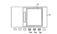
図1は、本発明に係る両面液晶表示装置を搭載した実施の形態1の折りたたみ式PDAの斜視図であり、(a)は蓋部を開いた状態の図、(b)は蓋部を閉じた状態の図である。図1(a)に示すように、PDA(Personal Digital Assistant:個人用の情報端末)10には、蓋部の内側面に5インチ(A=5inch)のメイン表示パネル11が配設され、これと蝶番で開閉可能に接続された本体部12にキーボードや各種制御部・処理部・記憶部等が搭載されている。そして、そのPDA10の蓋部を矢印C方向に閉じると、図1(b)に示すように、蓋部の背面に相当する外側面に2インチ(B=2inch)のサブ表示パネル13が配設されている。
【0019】
図2は、実施の形態1に係る図1のメイン表示パネルとサブ表示パネルの構成を説明する断面図である。図2に示すように、メイン表示パネル11とサブ表示パネル13のバックライト20は、共通の導光板27に対して側面方向から複数(ここでは7個)のLED(Light Emitting Diode:発光ダイオード)28a〜28gが線状に並設されていて、入射した光が導光板内に含有される微粒子で乱反射されて両面から光を発する。
【0020】
メイン表示パネル11は、2枚のガラス基板21,23の間に図示しない透明電極や配向膜を形成し、液晶23を封入した後、上下面に偏光板24,25を配置して形成される。また、サブ表示パネル13は、同様に2枚のガラス基板29,30の間に透明電極や配向膜が形成され、液晶31封入後に、上下面に偏光板32,33が配置されて形成されている。なお、実施の形態1では、バックライト20に共通の導光板27を用いており、メイン表示パネル11の表示面から見て、導光板27の反対側にサブ表示パネル13がある所と、無い所とがあり、光の透過状態が異なることで境界線が視認できるのを防止するため、液晶ディスプレイの無い導光板27の表面に遮光層34を形成している。
【0021】
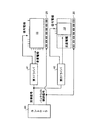
そして、図2に示すように、メイン表示パネル11は、バックライトとしての導光板27のLED28a〜28g(7個)を全点灯させた状態で画像表示を行い、サブ表示パネル13は、導光板27のLED28d〜28f(3個)を点灯させた状態で画像表示を行うようにする。図3は、メイン表示パネルの画像表示時におけるLEDの点灯状態を示した図であり、図4は、サブ表示パネルの画像表示時におけるLEDの点灯状態を示す図である。このLEDの切り替え処理は、次の図5に示すコントローラ40内で行っている。
【0022】
図5は、実施の形態1に係る両面液晶表示装置の画像表示の切り替え処理を行う構成図である。図5に示すように、メイン表示パネル11の画像表示処理は、第1ドライバ41で行い、サブ表示パネル13の画像表示処理は、第2ドライバ42で行っている。各ドライバ41,42は、コントローラ40からの画像信号に基づいて信号電極と走査電極に駆動電圧を印加することにより、画像表示が行われる。
【0023】
また、コントローラ40は、メイン表示パネル11とサブ表示パネル13の何れの画像表示を行うかによって、それぞれの液晶ディスプレイ位置と面積に応じたバックライト制御信号を出力する。このバックライト制御信号は、画像表示を行う液晶ディスプレイに対応した導光板のLEDを点灯させるものである。なお、この実施の形態1では、LEDの切り替え制御を何れの液晶ディスプレイで表示されるかにより行っているが、必ずしもこれに限定されるものではなく、例えば、図1のPDA10の蓋部の開閉部に磁石と磁気センサを装着し、蓋部の開閉時に発生する開閉信号に基づいてLEDの切り替え制御を行うようにしても良い。具体的には、蓋部が開いているときは(図1(a)の状態)、メイン表示パネル11に対応したLED(7個全部)を点灯させるように制御し、蓋部が閉じているときは(図1(b)の状態)、サブ表示パネル13に対応したLED(3個)を点灯させるように制御すればよい。
【0024】
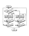
次に、図6は、実施の形態1の動作を説明するフローチャートである。図6に示すように、コントローラ40は、メイン表示パネル11とサブ表示パネル13の表示制御を行っているため、何れの表示パネルで画像表示しているかを判断することが可能である(ステップS100)。
【0025】
メイン表示パネル11でメイン表示を行っている場合は、ステップS101に移行して、コントローラ40がメイン表示パネル11に相当する7個のLEDを点灯させるように制御する(図3参照)。そして、表示パネルの表示が切り替わらない間は、ステップS101に戻って、当該LEDを点灯し続ける(ステップS102)。
【0026】
また、ステップS102において、表示パネルの切り替えが行われた場合は、ステップS103において表示終了か否かが判断され、表示終了でなければ上記ステップS100に戻って、メイン表示かサブ表示に応じてLEDの点灯制御が繰り返し行われる。
【0027】
さらに、ステップS100において、サブ表示パネル13でサブ表示を行っている場合は、ステップS104に移行して、コントローラ40がサブ表示パネル13に相当する3個のLEDを点灯させるように制御する(図4参照)。そして、表示パネルの表示が切り替わらない間は、ステップS104に戻って、当該LEDを点灯し続ける(ステップS105)。
【0028】
また、ステップS105において、表示パネルの切り替えが行われた場合は、ステップS106において表示終了か否かが判断され、表示終了でなければ上記ステップS100に戻って、メイン表示かサブ表示に応じてLEDの点灯制御が繰り返し行われる。そして、上記したステップS103およびステップS106において、表示終了の場合は、LEDの点灯制御もこれに対応して終了する。
【0029】
以上、説明したように、本実施の形態1によれば、メイン表示パネル11とサブ表示パネル13は、共通する1枚の導光板27を介して両面に配置されているため、両面液晶表示装置のトータルの厚さが薄型化できると共に、部品点数が大幅に削減でき、コストの低減が可能になる。
【0030】
また、本実施の形態1によれば、画像表示がメイン表示パネル11あるいはサブ表示パネル13で行われているかによって、その表示パネルの面積と位置に応じたLEDの点灯制御を行っている。これによって、画像表示に必要なバックライト領域のLEDのみを点灯させることができるため、バックライトの消費電力量を必要最低限にまで低減することができる。例えば、実施の形態1では、全部のLEDの数が7個あって、サブ表示パネルで画像表示を行うときは、3個に減らすことができるため、消費電力を57%程度低減することができる。
【0031】
さらに、本実施の形態1によれば、導光板27を介して反対側に液晶表示パネルがある領域と、無い領域とで境界線が目立つことがあったが、図2に示すように遮光層34を形成することにより、境界線が目立たなくなり、適正な画像表示を行うことができる。加えて、(図示は省略するが、)導光板27表面全面に半透過反射層(ハーフミラー、又は反射偏光子)を配設し、さらに上記遮光層34を配設する構成とすれば、半透過反射層で大半のバックライト光は反射されるため液晶表示パネルの偏光板と遮光層34による吸収の差の影響をさらに低減され、液晶表示パネルの境界線はさらに目立たなくなると共に、半透過反射層(ハーフミラー、又は反射偏光子)による反射により液晶表示パネル11側の表面輝度が向上する。この場合の配置構成の順は、両面光源側から半透過反射層(ハーフミラー又は反射偏光子)、遮光膜、液晶表示パネルの順となる。また、上記ハーフミラーとは金属膜を所定の膜厚で薄膜形成し、膜厚の制御によって入射する光の反射と透過の割合を適宜設定し得るものであり、上記反射偏光子とは入射した光の所定の偏光成分の光を反射し、それ以外の偏光成分の光を透過するものである(例えば、3M社のD-BEF、日東電工のPCF等)。
【0032】
また、本実施の形態1によれば、PDA10の蓋部の開閉動作に応じてLEDの点灯制御を行うようにすることができるため、開閉動作と連動して表示を切り替える場合は、開閉動作と連動してLEDの点灯制御を行うだけで、容易に制御することができる。
【0033】
(実施の形態2)
図7は、実施の形態2に係るメイン表示パネルとサブ表示パネルの構成を説明する断面図である。図7では、図2と同一部または相当部に同一符号を付して、構成説明を省略する。この実施の形態2の特徴的な構成は、メイン表示パネル11とサブ表示パネル13とが同じ大きさのパネルで構成されていて、位置だけがずれている場合についても、本発明によればバックライト点灯に必要なLEDの消費電力を低減することができる。
【0034】
これを図7で見ると、メイン表示パネル11とサブ表示パネル13の何れか一方の表示制御を行う場合に、従来例では常に6個のLED全てを点灯させる必要があった。しかし、本実施の形態2によれば、メイン表示パネル11で画像表示する場合、あるいは、サブ表示パネル13で画像表示する場合には、何れも4個のLEDを点灯させるだけでよいため、消費電力を33%程度低減する効果が得られる。
【0035】
また、この実施の形態2によれば、図7に示すように、液晶表示パネルの無い部分に遮光層34を形成したため、導光板27を介して反対側に液晶表示パネルがある領域と、無い領域とで境界線が目立たなくなり、適正な画像表示を行うことができる。加えて、導光板27表面全面にハーフミラーを配設し、さらに遮光層34を配設する構成とすれば、ハーフミラーで大半のバックライト光は反射されるため液晶表示パネルの偏光板と遮光層34による吸収の差の影響をさらに低減され、液晶表示パネルの境界線はさらに目立たなくなる。
【0036】
(実施の形態3)
図8は、実施の形態3に係るメイン表示パネルとサブ表示パネルの構成を説明する断面図である。図8では、図2と同一部または相当部に同一符号を付して、構成説明を省略する。この実施の形態3の特徴的な構成は、メイン表示パネル11よりもサブ表示パネル13の方が大きいパネルで構成されており、相互に重ならない位置に配置されている場合である。この場合についても、本発明によればバックライト点灯に必要なLEDの消費電力を低減することができる。
【0037】
これを図8で見ると、メイン表示パネル11とサブ表示パネル13の何れか一方の表示制御を行う場合に、従来例では常に6個のLED全てを点灯させる必要があった。しかし、本実施の形態3によれば、メイン表示パネル11で画像表示する場合は2個のLED、サブ表示パネル13で画像表示する場合は、4個のLEDを点灯させるため、消費電力はそれぞれ66%と33%程度低減させる効果が得られる。
【0038】
また、この実施の形態3によれば、図8に示すように、液晶表示パネルの無い部分に遮光層34を形成している。この実施の形態3では相互に液晶パネルが重なり合っていないため、境界線は目立たないが、透過光を遮光することにより適正な画像表示を行うことができる。
【0039】
(実施の形態4)
図9は、実施の形態4において両面光源としてエレクトロルミネッセンス素子を用いた場合の断面構成図である。図9に示すように、透明基板50の表面にITO等の透明導電材料からなる透明電極(陽極)51が形成され、正孔輸送層、発光層、電子輸送層、更にはITO等の透明導電部材からなる透明電極(陰極)53が順次積層されてエレクトロルミネッセンス素子が構成されている。実施の形態4では、このエレクトロルミネッセンス素子60,61,62を一定の領域毎に形成し、それぞれの透明電極51,53間に一定の電圧を電源63により印加すると、有機層52全体が発光するものである。ここでは、透明電極51,53を使い、透明基板50上に形成しているため、光は上下両面から発せられることになる。
【0040】
図10は、図9のエレクトロルミネッセンス素子を用いてメイン表示パネルのバックライトとして用いた場合の図である。図10に示すように、スイッチ70,71,72を全て閉じることにより、全てのエレクトロルミネッセンス素子60,61,62が発光して、メイン表示パネル11のバックライトとして用いることができる。
【0041】
また、図11は、図9のエレクトロルミネッセンス素子を用いてサブ表示パネルのバックライトとして用いた場合の図である。図11に示すように、スイッチ70,71,72のうち、スイッチ71のみを閉じて、他を開くことにより、真中のエレクトロルミネッセンス素子61のみを発光させることが可能となる。このため、サブ表示パネル13のバックライトとして用いることができる。
【0042】
このように、実施の形態4によれば、エレクトロルミネッセンス素子を用いて予め発光領域を形成しておけば、各領域に対して電圧制御を行うだけで発光領域を容易に制御することができる。特に、形成する発光領域の形状によっては、種々の形状や面積を自由に形成することができるため、非常に自由度が大きくなり、それだけ省電力効果も得ることができる。
【0043】
上記した図10および図11では、上記実施の形態1〜3で説明した遮光層34を図示していないが、実施の形態4の場合も同様であって、遮光層を設けることにより、液晶表示パネルの重なり具合に応じて境界線が目立つことなく、適正な画像表示を行うことができるようになる。
【0044】
以上説明したように、この発明によれば、両面光源をバックライトとして用いることにより、バックライトを薄型化しつつ、発光領域可変手段によって液晶表示パネルの配置位置と面積に応じて両面光源の発光領域が変えられるようにし、切替手段で発光領域可変手段を液晶表示パネルの表示タイミングに合わせて切り替えるようにしたので、液晶表示画面を切り替えて表示する際に要するバックライトの消費電力量を必要最低限とすることができる。
【0045】
また、本発明の好ましい態様によれば、発光領域可変手段として導光板に対して複数の発光手段を並設し、切替手段によって液晶表示パネルの表示タイミングに合わせて、複数の発光手段の中から液晶表示パネルの配置位置と面積に応じた発光手段を発光させるようにしたので、容易に発光領域を可変することができ、バックライトの消費電力量を必要最低限にできる。
【0046】
また、本発明の好ましい態様によれば、発光手段として点光源である発光ダイオードを用いたので、消費電力が低減できると共に、バックライトの色を自由に選択できる上、光源にかかるコストも低減することができる。
【0047】
また、本発明の好ましい態様によれば、導光板の表面には、レンズシートと拡散板の少なくとも一方が形成されているので、導光板から発する光の輝度をより一層高めることができる。
【0048】
また、本発明の好ましい態様によれば、両面光源として透明基板上に形成されたエレクトロルミネッセンス素子を用い、発光領域可変手段として、各発光領域毎にエレクトロルミネッセンス素子を個別に形成して、切替手段として、各液晶表示パネルの表示タイミングに合わせて液晶表示パネルの配置位置と面積に対応したエレクトロルミネッセンス素子を発光させるように切り替えるので、低消費電力化できると共に、バックライトの色が自由に選択できる上、発光領域の形状を自由に形成することができる。
【0049】
また、本発明の好ましい態様によれば、液晶表示パネルを開閉可能な蓋部の内側面と外側面に配置し、切替手段によって発光領域可変手段を蓋部の開閉状態に合わせて切り替えるようにしたので、蓋部の開閉状態に応じて表示を切り替える場合は、容易かつ確実にバックライトの切り替えを行うことができる。
【0050】
また、本発明の好ましい態様によれば、一方の液晶表示パネルと両面光源との間に配置された遮光層は、液晶表示パネル以外の部分の領域に配置するようにしたので、両面光源を介して反対側の液晶表示パネルの境界線が透けて見えなくなり、綺麗な画像表示を行うことができる。また、他の構成として一方の液晶表示パネルと両面光源との間に、ハーフミラーや反射偏光子と言った半透過反射層を配置した構成でもよく、更にこの構成において、ハーフミラーや反射偏光子と液晶表示パネルとの間に上記遮光層を配置することにより、反対側の液晶表示パネルの境界線が透けて見えなくなり、綺麗な画像表示を行うことができる。
【図面の簡単な説明】
【図1】 本発明に係る両面液晶表示装置を搭載した実施の形態1の折りたたみ式PDAの斜視図であり、(a)は蓋部を開いた状態の図、(b)は蓋部を閉じた状態の図である。
【図2】 実施の形態1に係る図1のメイン表示パネルとサブ表示パネルの構成を説明する断面図である。
【図3】 メイン表示パネルの画像表示時におけるLEDの点灯状態を示した図である。
【図4】 サブ表示パネルの画像表示時におけるLEDの点灯状態を示す図である。
【図5】 実施の形態1に係る両面液晶表示装置の画像表示の切り替え処理を行う構成図である。
【図6】 実施の形態1の動作を説明するフローチャートである。
【図7】 実施の形態2に係るメイン表示パネルとサブ表示パネルの構成を説明する断面図である。
【図8】 実施の形態3に係るメイン表示パネルとサブ表示パネルの構成を説明する断面図である。
【図9】 実施の形態4において両面光源としてエレクトロルミネッセンス素子を用いた場合の断面構成図である。
【図10】 図9のエレクトロルミネッセンス素子を用いてメイン表示パネルのバックライトとして用いた場合の図である。
【図11】 図9のエレクトロルミネッセンス素子を用いてサブ表示パネルのバックライトとして用いた場合の図である。
【符号の説明】
10 PDA、11 メイン表示パネル、12 本体部、13 サブ表示パネル、20 バックライト、21,22,29,30 ガラス基板、23,31 液晶、24,25,32,33 偏光板、27 導光板、28a〜28g LED、34 遮光層、40 コントローラ、41 第1ドライバ、42 第2ドライバ、50 透明基板、51,53 透明電極、52 発光層、60,61,62
エレクトロルミネッセンス素子、63 電源、70,71,72 スイッチ[0001]
BACKGROUND OF THE INVENTION
The present invention relates to a double-sided liquid crystal display device, and in particular, a double-sided liquid crystal display in which a liquid crystal display panel is disposed at an arbitrary place on each side using a double-sided light source that emits light on both sides as a backlight and the liquid crystal display panel is switched. It relates to the device.
[0002]
[Prior art]
2. Description of the Related Art Conventionally, a double-sided liquid crystal display device in which two liquid crystal display devices are arranged back to back on an inner surface and an outer surface of an information portable terminal such as a mobile phone or a PDA (Personal Digital Assistant) having an openable / closable lid has been used. Yes. Conventionally, two liquid crystal display units each composed of a liquid crystal display panel with a backlight are prepared and arranged back to back.
[0003]
In addition, in order to reduce the thickness occupied by the backlights of the liquid crystal display panels arranged on both sides of the lid, etc., the cross sections of the light guide plates of the backlights of the two liquid crystal display panels are respectively wedge-shaped, Some backlights are made thin by irradiating light from light sources arranged on both sides with the inclined surfaces facing each other (see Patent Document 1).
[0004]
Furthermore, in order to reduce the thickness occupied by the backlight of the liquid crystal display panel arranged on both sides of the lid, etc., the backlight of the liquid crystal display panel is made thinner by adopting a common light guide plate capable of emitting light on both sides. There was a thing (refer patent document 2).
[0005]
[Patent Document 1]
JP 2002-244133 A
[Patent Document 2]
JP 2001-67049 A
[0006]
[Problems to be solved by the invention]
However, in such a double-sided liquid crystal display device, if two liquid crystal display units each composed of a backlit liquid crystal display panel are arranged back to back, the thickness becomes very thick and the portability of the information terminal is impaired. Result.
[0007]
Therefore, as described in Patent Document 1 described above, the two light guide plates can be thinned to a certain extent by overlapping them in a wedge shape, but the two light guide plates are overlapped in a state where a reflection sheet is formed on each inclined surface. There was a problem that the thickness would need to be matched and the thickness would increase accordingly. In recent years, thinning has progressed, and the inclination angle can hardly be obtained, and the processing of the light guide plate becomes complicated, but there is also a problem that the effect is hardly obtained.
[0008]
In the case of Patent Document 2 described above, the backlight can be made thin by adopting a common light guide plate capable of light emission on both sides. However, as shown in FIGS. 4 and 5 in Patent Document 2, when the display areas of the first liquid crystal display device and the second liquid crystal display device are greatly different, a liquid crystal display device having a small display area (here, Even when only the second liquid crystal display device is displayed, the entire common light guide plate has to be turned on, and there is a problem that wasteful power is consumed. As a result, the waste of power consumption increases as the display area ratio of the two liquid crystal display devices increases.
[0009]
The present invention has been made in order to solve the above-described problems. When a liquid crystal display panel is arranged on both sides, the consumption required for a backlight when switching and displaying a liquid crystal display screen while maintaining a thin thickness is provided. An object is to provide a double-sided liquid crystal display device capable of minimizing the amount of electric power.
[0010]
[Means for Solving the Problems]
In order to solve the above-described problems and achieve the object, the present invention is a double-sided light source that emits light from both sides of a sheet, and the double-sided light source is used as a backlight at least one at each location on each side, A liquid crystal display panel capable of displaying an image, a light emitting area variable means for changing a light emitting area of the double-sided light source in accordance with an arrangement position and an area of the liquid crystal display panel, and the light emitting area variable means for the liquid crystal display panel And switching means for switching in accordance with the display timing. As a result, the backlight is made thin by using the double-sided light source as the backlight, and the light-emitting area variable means can change the light-emitting area of the double-sided light source according to the arrangement position and area of the liquid crystal display panel, and the switching means emits light. Since the region varying means is switched in accordance with the display timing of the liquid crystal display panel, the power consumption of the backlight required for switching and displaying the liquid crystal display screen can be minimized.
[0011]
According to a preferred aspect of the present invention, the double-sided light source includes at least a light source and a light guide plate, and the light emitting region variable means includes a plurality of light emitting means arranged in parallel to the light guide plate, and the switching means. Is characterized in that switching is performed so that the light emitting means according to the arrangement position and area of each liquid crystal display panel emit light according to the display timing of the liquid crystal display panel. Accordingly, a plurality of light emitting means are arranged in parallel with the light guide plate as the light emitting region variable means, and the arrangement position and area of the liquid crystal display panel are selected from the plurality of light emitting means according to the display timing of the liquid crystal display panel by the switching means. Since the light emitting means corresponding to the light is made to emit light, the light emitting area can be easily changed, and the power consumption of the backlight can be minimized.
[0012]
Also, according to a preferred aspect of the present invention, the light emitting means is a light emitting diode, and a surface light source is configured by arranging a plurality of light emitting diodes in a line from the side surface of the light guide plate. To do. Thereby, since the light emitting diode which is a point light source is used as the light emitting means, the power consumption can be reduced, the color of the backlight can be freely selected, and the cost of the light source can be reduced.
[0013]
Further, according to a preferred aspect of the present invention, at least one of a lens sheet and a diffusion plate is further formed on the surface of the light guide plate. Thereby, since at least one of a lens sheet (prism sheet) and a diffusion plate is formed on the surface of the light guide plate, the luminance of light emitted from the light guide plate can be further increased.
[0014]
Further, according to a preferred aspect of the present invention, the double-sided light source is an electroluminescence element formed on a transparent substrate and capable of emitting light on both sides, and the light-emitting region varying means is provided for each light-emitting region on the transparent substrate. The electroluminescent element is formed individually, and the switching means causes the electroluminescent element formed corresponding to the arrangement position and area of each liquid crystal display panel to emit light according to the display timing of each liquid crystal display panel. It is characterized by switching as follows. As a result, an electroluminescent element formed on a transparent substrate is used as a double-sided light source, an electroluminescent element is individually formed for each light emitting area as a light emitting area variable means, and a display on each liquid crystal display panel is used as a switching means. Since the electroluminescent device corresponding to the position and area of the liquid crystal display panel is switched to emit light according to the timing, the power consumption can be reduced, the backlight color can be freely selected, and the shape of the light emitting area can be freely selected. Can be formed.
[0015]
Further, according to a preferred aspect of the present invention, when the liquid crystal display panel is disposed on the inner side surface and the outer side surface of the lid portion that can be opened and closed, the switching means is configured such that the light emitting region varying means is connected to the lid portion. It is characterized by switching according to the open / closed state. As a result, the liquid crystal display panel is arranged on the inner side surface and the outer side surface of the lid portion that can be opened and closed, and the light emitting area changing means is switched according to the opening and closing state of the lid portion by the switching means. When switching the display, the backlight can be easily and reliably switched.
[0016]
According to a preferred aspect of the present invention, a light shielding layer is disposed between one of the liquid crystal display panels and the double-sided light source, and the light shielding layer is disposed in a region other than the liquid crystal display panel. It is characterized by that. As a result, the light-shielding layer disposed between the one liquid crystal display panel and the double-sided light source is arranged in a region other than the liquid crystal display panel. The line is not seen through and a clear image can be displayed. Further, as another configuration, a configuration in which a transflective layer such as a half mirror or a reflective polarizer is disposed between one liquid crystal display panel and a double-sided light source may be used. The light shielding layer may be disposed between the child and the liquid crystal display panel.
[0017]
DETAILED DESCRIPTION OF THE INVENTION
Embodiments of a double-sided liquid crystal display device according to the present invention will be described below in detail with reference to the drawings. In addition, this invention is not limited by this embodiment.
[0018]
(Embodiment 1)
FIG. 1 is a perspective view of a foldable PDA according to Embodiment 1 in which a double-sided liquid crystal display device according to the present invention is mounted. FIG. 1 (a) is a diagram showing a state in which a lid is opened, and FIG. FIG. As shown in FIG. 1 (a), a PDA (Personal Digital Assistant: personal information terminal) 10 is provided with a
[0019]
2 is a cross-sectional view illustrating the configuration of the main display panel and the sub display panel of FIG. 1 according to the first embodiment. As shown in FIG. 2, the
[0020]
The
[0021]
As shown in FIG. 2, the
[0022]
FIG. 5 is a configuration diagram for performing image display switching processing of the double-sided liquid crystal display device according to the first embodiment. As shown in FIG. 5, the image display process of the
[0023]
Further, the
[0024]
Next, FIG. 6 is a flowchart for explaining the operation of the first embodiment. As shown in FIG. 6, since the
[0025]
When the main display is being performed on the
[0026]
If the display panel is switched in step S102, it is determined in step S103 whether or not the display is finished. If the display is not finished, the process returns to step S100 and the LED is displayed according to the main display or the sub display. The lighting control is repeatedly performed.
[0027]
Furthermore, when the sub display is being performed on the
[0028]
If the display panel is switched in step S105, it is determined in step S106 whether or not the display is finished. If the display is not finished, the process returns to step S100 and the LED is displayed according to the main display or the sub display. The lighting control is repeatedly performed. And in above-mentioned step S103 and step S106, in the case of a display end, the lighting control of LED is also complete | finished corresponding to this.
[0029]
As described above, according to the first embodiment, since the
[0030]
Further, according to the first embodiment, depending on whether the image display is performed on the
[0031]
Furthermore, according to the first embodiment, a boundary line may be conspicuous between the area where the liquid crystal display panel is located on the opposite side and the area where the liquid crystal display panel is not located via the
[0032]
Further, according to the first embodiment, since the lighting control of the LED can be performed according to the opening / closing operation of the lid portion of the
[0033]
(Embodiment 2)
FIG. 7 is a cross-sectional view illustrating the configuration of the main display panel and the sub display panel according to the second embodiment. 7, the same reference numerals are given to the same or corresponding parts as in FIG. The characteristic configuration of the second embodiment is that, even when the
[0034]
As shown in FIG. 7, when performing display control of either the
[0035]
Further, according to the second embodiment, as shown in FIG. 7, since the
[0036]
(Embodiment 3)
FIG. 8 is a cross-sectional view illustrating the configuration of the main display panel and the sub display panel according to the third embodiment. In FIG. 8, the same reference numerals are assigned to the same or corresponding parts as in FIG. The characteristic configuration of the third embodiment is a case where the
[0037]
As shown in FIG. 8, when performing display control of either the
[0038]
Further, according to the third embodiment, as shown in FIG. 8, the
[0039]
(Embodiment 4)
FIG. 9 is a cross-sectional configuration diagram when an electroluminescence element is used as a double-sided light source in the fourth embodiment. As shown in FIG. 9, a transparent electrode (anode) 51 made of a transparent conductive material such as ITO is formed on the surface of a
[0040]
FIG. 10 is a diagram when the electroluminescence element of FIG. 9 is used as a backlight of a main display panel. As shown in FIG. 10, by closing all the
[0041]
FIG. 11 is a diagram showing a case where the electroluminescence element of FIG. 9 is used as a backlight of a sub display panel. As shown in FIG. 11, by closing only the
[0042]
As described above, according to the fourth embodiment, if the light emitting region is formed in advance using the electroluminescence element, the light emitting region can be easily controlled only by performing voltage control on each region. In particular, depending on the shape of the light emitting region to be formed, various shapes and areas can be freely formed. Therefore, the degree of freedom is greatly increased, and a power saving effect can be obtained.
[0043]
10 and 11, the
[0044]
As described above, according to the present invention, by using the double-sided light source as the backlight, the light-emitting area of the double-sided light source is reduced according to the arrangement position and area of the liquid crystal display panel by the light-emitting area changing means while thinning the backlight. Since the light emitting area changing means is switched by the switching means in accordance with the display timing of the liquid crystal display panel, the power consumption of the backlight required for switching and displaying the liquid crystal display screen is minimized. It can be.
[0045]
Further, according to a preferred aspect of the present invention, a plurality of light emitting means are juxtaposed to the light guide plate as the light emitting region varying means, and the switching means adjusts the display timing of the liquid crystal display panel from among the plurality of light emitting means. Since the light emitting means according to the arrangement position and area of the liquid crystal display panel emits light, the light emitting area can be easily changed, and the power consumption of the backlight can be minimized.
[0046]
Further, according to the preferred embodiment of the present invention, since the light emitting diode as a point light source is used as the light emitting means, the power consumption can be reduced, the color of the backlight can be freely selected, and the cost of the light source is also reduced. be able to.
[0047]
According to a preferred aspect of the present invention, since at least one of the lens sheet and the diffusion plate is formed on the surface of the light guide plate, the luminance of light emitted from the light guide plate can be further increased.
[0048]
Further, according to a preferred aspect of the present invention, the electroluminescent element formed on the transparent substrate is used as the double-sided light source, the electroluminescent element is individually formed for each light emitting area as the light emitting area variable means, and the switching means. Since the electroluminescence element corresponding to the arrangement position and area of the liquid crystal display panel is switched to emit light according to the display timing of each liquid crystal display panel, the power consumption can be reduced and the color of the backlight can be freely selected In addition, the shape of the light emitting region can be freely formed.
[0049]
Further, according to a preferred aspect of the present invention, the liquid crystal display panel is arranged on the inner side surface and the outer side surface of the lid portion that can be opened and closed, and the light emitting area changing means is switched by the switching means according to the open / closed state of the lid portion. Therefore, when switching the display according to the open / closed state of the lid, it is possible to easily and reliably switch the backlight.
[0050]
According to a preferred aspect of the present invention, the light shielding layer disposed between the one liquid crystal display panel and the double-sided light source is arranged in a region other than the liquid crystal display panel. Thus, the border line of the opposite side liquid crystal display panel can not be seen through, and a beautiful image display can be performed. Another configuration may be a configuration in which a transflective layer such as a half mirror or a reflective polarizer is disposed between one liquid crystal display panel and a double-sided light source. In this configuration, the half mirror or the reflective polarizer is also included. By disposing the light shielding layer between the liquid crystal display panel and the liquid crystal display panel, the boundary line of the liquid crystal display panel on the opposite side cannot be seen through, and a clear image display can be performed.
[Brief description of the drawings]
FIG. 1 is a perspective view of a foldable PDA according to Embodiment 1 in which a double-sided liquid crystal display device according to the present invention is mounted. FIG. 1 (a) is a view showing a state in which a lid is opened, and FIG. FIG.
2 is a cross-sectional view illustrating a configuration of a main display panel and a sub display panel in FIG. 1 according to Embodiment 1. FIG.
FIG. 3 is a diagram showing a lighting state of an LED when an image is displayed on a main display panel.
FIG. 4 is a diagram showing a lighting state of an LED when an image is displayed on a sub display panel.
FIG. 5 is a configuration diagram for performing image display switching processing of the double-sided liquid crystal display device according to the first embodiment;
FIG. 6 is a flowchart for explaining the operation of the first embodiment.
7 is a cross-sectional view illustrating configurations of a main display panel and a sub display panel according to Embodiment 2. FIG.
8 is a cross-sectional view illustrating configurations of a main display panel and a sub display panel according to Embodiment 3. FIG.
9 is a cross-sectional configuration diagram in the case where an electroluminescence element is used as a double-sided light source in Embodiment 4. FIG.
10 is a diagram of the case where the electroluminescence element of FIG. 9 is used as a backlight of a main display panel.
FIG. 11 is a diagram showing a case where the electroluminescence element of FIG. 9 is used as a backlight of a sub display panel.
[Explanation of symbols]
10 PDA, 11 main display panel, 12 main body, 13 sub display panel, 20 backlight, 21, 22, 29, 30 glass substrate, 23, 31 liquid crystal, 24, 25, 32, 33 polarizing plate, 27 light guide plate, 28a to 28g LED, 34 light shielding layer, 40 controller, 41 first driver, 42 second driver, 50 transparent substrate, 51, 53 transparent electrode, 52 light emitting layer, 60, 61, 62
Electroluminescence element, 63 power supply, 70, 71, 72 switch
Claims (4)
前記両面光源をバックライトとして該両面光源の一方の面及び該一方の面の反対の面に少なくとも1つずつ配置され、画像表示可能な複数の液晶表示パネルと、
前記液晶表示パネルの配置位置と面積に応じて前記両面光源の発光領域が変えられるようにした発光領域可変手段と、
前記発光領域可変手段を前記液晶表示パネルの表示タイミングに合わせて切り替える切替手段と、を備え、
前記両面光源の一方の面に設けられた前記液晶表示パネルと前記両面光源の一方の面の反対の面に設けられた前記液晶表示パネルとが、前記両面光源の一部を共有し、
前記両面光源は、透明基板上に形成された両面発光可能なエレクトロルミネッセンス素子であり、前記透明基板上の各発光領域毎にエレクトロルミネッセンス素子を個別に形成したもので、
前記両面光源の一方の面に設けられた前記液晶表示パネルと前記両面光源の一方の面の反対の面に設けられた前記液晶表示パネルとが、前記エレクトロルミネッセンス素子の一部を共有し、
前記切替手段は、各液晶表示パネルの表示タイミングに合わせて、各液晶表示パネルの配置位置と面積に対応して形成されたエレクトロルミネッセンス素子を発光させるように切り替えることを特徴とする両面液晶表示装置。A double-sided light source that emits light from both sides of the sheet,
A plurality of liquid crystal display panels arranged to display at least one image on one side of the double-sided light source and on the opposite side of the one side, using the double-sided light source as a backlight;
A light emitting region variable means for changing the light emitting region of the double-sided light source according to the arrangement position and area of the liquid crystal display panel;
Switching means for switching the light emitting region variable means in accordance with the display timing of the liquid crystal display panel,
The liquid crystal display panel provided on one side of the double-sided light source and the liquid crystal display panel provided on the opposite side of the one side of the double-sided light source share a part of the double-sided light source,
The double-sided light source is an electroluminescent element capable of emitting light on both sides formed on a transparent substrate, and an electroluminescent element is individually formed for each light emitting region on the transparent substrate,
The liquid crystal display panel provided on one side of the double-sided light source and the liquid crystal display panel provided on the opposite side of the one side of the double-sided light source share a part of the electroluminescence element,
The double-sided liquid crystal display device characterized in that the switching means switches so that the electroluminescence element formed corresponding to the arrangement position and area of each liquid crystal display panel emits light in accordance with the display timing of each liquid crystal display panel .
前記切替手段は、前記発光領域可変手段を前記蓋部の開閉状態に合わせて切り替えることを特徴とする請求項1に記載の両面液晶表示装置。When the liquid crystal display panel is disposed on the inner and outer surfaces of the lid that can be opened and closed,
The double-sided liquid crystal display device according to claim 1, wherein the switching unit switches the light emitting region varying unit in accordance with an open / closed state of the lid.
Priority Applications (5)
| Application Number | Priority Date | Filing Date | Title |
|---|---|---|---|
| JP2003204700A JP3873940B2 (en) | 2003-07-31 | 2003-07-31 | Double-sided liquid crystal display |
| US10/889,136 US7365730B2 (en) | 2003-07-31 | 2004-07-13 | Double-sided liquid crystal display device |
| TW093122569A TWI282888B (en) | 2003-07-31 | 2004-07-28 | Double-sided liquid crystal display device |
| KR1020040059647A KR100637960B1 (en) | 2003-07-31 | 2004-07-29 | Double-sided liquid crystal display device |
| CNB200410070266XA CN100410765C (en) | 2003-07-31 | 2004-07-30 | Two-side liquid crystal display |
Applications Claiming Priority (1)
| Application Number | Priority Date | Filing Date | Title |
|---|---|---|---|
| JP2003204700A JP3873940B2 (en) | 2003-07-31 | 2003-07-31 | Double-sided liquid crystal display |
Publications (2)
| Publication Number | Publication Date |
|---|---|
| JP2005049522A JP2005049522A (en) | 2005-02-24 |
| JP3873940B2 true JP3873940B2 (en) | 2007-01-31 |
Family
ID=34225019
Family Applications (1)
| Application Number | Title | Priority Date | Filing Date |
|---|---|---|---|
| JP2003204700A Expired - Lifetime JP3873940B2 (en) | 2003-07-31 | 2003-07-31 | Double-sided liquid crystal display |
Country Status (5)
| Country | Link |
|---|---|
| US (1) | US7365730B2 (en) |
| JP (1) | JP3873940B2 (en) |
| KR (1) | KR100637960B1 (en) |
| CN (1) | CN100410765C (en) |
| TW (1) | TWI282888B (en) |
Families Citing this family (30)
| Publication number | Priority date | Publication date | Assignee | Title |
|---|---|---|---|---|
| JP2007514313A (en) * | 2003-12-15 | 2007-05-31 | コーニンクレッカ フィリップス エレクトロニクス エヌ ヴィ | Backlight device |
| KR20060021056A (en) * | 2004-09-02 | 2006-03-07 | 삼성전자주식회사 | Display device and driving method thereof |
| JP2006260853A (en) * | 2005-03-15 | 2006-09-28 | Fuji Photo Film Co Ltd | Lighting device |
| JP2006269210A (en) * | 2005-03-23 | 2006-10-05 | Nidec Copal Corp | Surface light source device |
| JP4017007B2 (en) * | 2005-03-29 | 2007-12-05 | エプソンイメージングデバイス株式会社 | Electro-optical device and electronic apparatus including the electro-optical device |
| JP2006350338A (en) * | 2005-06-13 | 2006-12-28 | Samsung Electronics Co Ltd | Backlight assembly, and display device having the same,and a method for adjusting luminance of the same |
| KR100908026B1 (en) * | 2005-06-22 | 2009-07-15 | 후지쯔 가부시끼가이샤 | Display unit, display device, and information processing device |
| TW200705005A (en) * | 2005-07-22 | 2007-02-01 | Ind Tech Res Inst | Liquid crystal display |
| JP4671117B2 (en) * | 2005-09-22 | 2011-04-13 | ミネベア株式会社 | Illumination device and light source unit using the same |
| KR100743295B1 (en) * | 2005-10-28 | 2007-07-26 | 엘지전자 주식회사 | Method and apparatus of controlling back light |
| KR101205535B1 (en) * | 2005-12-06 | 2012-11-27 | 삼성디스플레이 주식회사 | Apparatus for driving of light source and display device having the same and method of driving of light source |
| KR20070062689A (en) * | 2005-12-13 | 2007-06-18 | 삼성전자주식회사 | Liquid crystal display and driving method for the same |
| JP4702167B2 (en) * | 2006-05-09 | 2011-06-15 | 豊田合成株式会社 | Liquid crystal display device |
| US7972051B2 (en) * | 2006-09-21 | 2011-07-05 | Motorola Mobility, Inc. | Double-sided backlight and assembly incorporating a double-sided light source coupling light guide |
| US7461962B2 (en) | 2007-01-22 | 2008-12-09 | Samsung Electronics Co., Ltd. | Backlight assembly, display device provided with the same, and method thereof |
| JP4952286B2 (en) * | 2007-02-15 | 2012-06-13 | 船井電機株式会社 | Information display device |
| KR101337258B1 (en) * | 2007-02-21 | 2013-12-05 | 삼성디스플레이 주식회사 | Liquid crystal display |
| KR100892368B1 (en) * | 2007-02-26 | 2009-04-10 | 주식회사 나모텍 | Liquid Crystal Display Device And Method For Manufacturing The Same |
| CN101436423B (en) * | 2007-11-15 | 2011-01-26 | 鸿富锦精密工业(深圳)有限公司 | Dvd player and display control method thereof |
| JP2009222951A (en) * | 2008-03-17 | 2009-10-01 | Sanyo Electric Co Ltd | Display |
| WO2009139236A1 (en) * | 2008-05-13 | 2009-11-19 | シャープ株式会社 | Light emitting device and liquid crystal display device |
| JP5328230B2 (en) | 2008-06-10 | 2013-10-30 | キヤノン株式会社 | Cartridge and electrophotographic image forming apparatus using the cartridge |
| JP2010060817A (en) * | 2008-09-03 | 2010-03-18 | Olympus Corp | Display device and electronic apparatus with the same |
| RU2642505C2 (en) * | 2010-12-10 | 2018-01-25 | Йота Девайсез Ипр Лтд | Mobile device with user interface |
| TWI528154B (en) * | 2011-05-27 | 2016-04-01 | 緯創資通股份有限公司 | Clamshell electronic device, switching module and switching method |
| US9230510B1 (en) * | 2013-09-20 | 2016-01-05 | American Megatrends, Inc. | Double-sided display devices |
| KR102168671B1 (en) * | 2014-09-24 | 2020-10-22 | 삼성디스플레이 주식회사 | Dual display device and electronic device having the same |
| KR102479097B1 (en) | 2015-08-27 | 2022-12-20 | 삼성디스플레이 주식회사 | Display device |
| JP2019101284A (en) * | 2017-12-05 | 2019-06-24 | シャープ株式会社 | Display device |
| KR102454195B1 (en) | 2018-05-14 | 2022-10-13 | 삼성디스플레이 주식회사 | Foldable display device |
Family Cites Families (16)
| Publication number | Priority date | Publication date | Assignee | Title |
|---|---|---|---|---|
| JPH08184821A (en) | 1994-12-28 | 1996-07-16 | Sharp Corp | Display device |
| JP2000075802A (en) | 1998-08-26 | 2000-03-14 | Matsushita Electric Ind Co Ltd | Back light device and back light element |
| JP2000155309A (en) | 1998-11-20 | 2000-06-06 | Matsushita Electric Ind Co Ltd | Color display device and communication apparatus using the same |
| KR100444694B1 (en) | 1999-08-04 | 2004-08-18 | 엘지전자 주식회사 | Apparatus For Liquid Crystal Display in A Folder Form Mobile Telecommunication Terminal |
| US6574487B1 (en) | 2000-02-23 | 2003-06-03 | Motorola, Inc. | Communication device with a dual-sided liquid crystal display |
| JP2002244133A (en) | 2001-02-21 | 2002-08-28 | Nec Access Technica Ltd | Double-sided liquid crystal display |
| JP3700611B2 (en) | 2001-06-07 | 2005-09-28 | セイコーエプソン株式会社 | Transflective electro-optical device and electronic apparatus |
| JP2002372711A (en) | 2001-06-14 | 2002-12-26 | Seiko Instruments Inc | Liquid crystal display device |
| JP3645201B2 (en) | 2001-07-09 | 2005-05-11 | タカヤマ金属工業株式会社 | Bundle member |
| JP3760900B2 (en) | 2001-09-06 | 2006-03-29 | セイコーエプソン株式会社 | Light guiding device, electro-optical device, and electronic apparatus |
| JP2003098545A (en) | 2001-09-20 | 2003-04-03 | Sharp Corp | Double-sided display type liquid crystal display device and portable electronic apparatus provided with the same |
| WO2003029884A1 (en) | 2001-09-28 | 2003-04-10 | Citizen Watch Co., Ltd. | Liquid crystal display device |
| JP3760839B2 (en) * | 2001-11-09 | 2006-03-29 | 株式会社日立製作所 | Communication terminal device |
| US7064740B2 (en) * | 2001-11-09 | 2006-06-20 | Sharp Laboratories Of America, Inc. | Backlit display with improved dynamic range |
| US7034799B2 (en) * | 2001-12-14 | 2006-04-25 | Samsung Electronics Co., Ltd. | Backlighting device for dual liquid crystal display and folder-type mobile phone therewith |
| KR100887635B1 (en) * | 2002-09-26 | 2009-03-11 | 삼성전자주식회사 | Back light assembly and liquid crystal display device using the same |
-
2003
- 2003-07-31 JP JP2003204700A patent/JP3873940B2/en not_active Expired - Lifetime
-
2004
- 2004-07-13 US US10/889,136 patent/US7365730B2/en active Active
- 2004-07-28 TW TW093122569A patent/TWI282888B/en active
- 2004-07-29 KR KR1020040059647A patent/KR100637960B1/en active IP Right Grant
- 2004-07-30 CN CNB200410070266XA patent/CN100410765C/en active Active
Also Published As
| Publication number | Publication date |
|---|---|
| US20050052383A1 (en) | 2005-03-10 |
| KR20050014706A (en) | 2005-02-07 |
| US7365730B2 (en) | 2008-04-29 |
| TW200513746A (en) | 2005-04-16 |
| CN100410765C (en) | 2008-08-13 |
| CN1580907A (en) | 2005-02-16 |
| JP2005049522A (en) | 2005-02-24 |
| KR100637960B1 (en) | 2006-10-23 |
| TWI282888B (en) | 2007-06-21 |
Similar Documents
| Publication | Publication Date | Title |
|---|---|---|
| JP3873940B2 (en) | Double-sided liquid crystal display | |
| US6954239B2 (en) | Display unit | |
| US7538834B2 (en) | Display device and electronic apparatus | |
| TWI334041B (en) | Display device and electronic device having the same | |
| US8049840B2 (en) | Double-sided display apparatus | |
| US7796215B2 (en) | Double sided liquid crystal display unit and portable electronic apparatus comprising a polarizing element between two liquid crystal display panels | |
| US20140293188A1 (en) | Displays with Local Dimming Elements | |
| KR20090003356A (en) | Image display | |
| TWI257514B (en) | Display | |
| JP2007232882A (en) | Display device and electronic apparatus | |
| US8325290B2 (en) | Dual liquid crystal display device | |
| JP2005148740A (en) | Reflection type liquid crystal display of dual display | |
| JP2002196705A (en) | Image display device | |
| JP3980889B2 (en) | Display device and portable information terminal device | |
| JP2002303863A (en) | Liquid crystal display device | |
| JP4333220B2 (en) | LIGHTING DEVICE, ELECTRO-OPTICAL DEVICE, LIGHTING DEVICE MANUFACTURING METHOD, ELECTRO-OPTICAL DEVICE MANUFACTURING METHOD, AND ELECTRONIC DEVICE | |
| KR20070076652A (en) | Reversible liquid crystal display and handy terminal having the same | |
| US7916243B2 (en) | Dual liquid crystal display device | |
| JP2004127622A (en) | Lighting device, liquid crystal display, and portable information device | |
| KR20070078885A (en) | Liquid crystal panel and two-way liquid crystal display using the same | |
| KR20060060336A (en) | A flat display device provided with a new type reflector sheet | |
| KR20080008744A (en) | Dual side liquid crystal display | |
| KR20030049943A (en) | A reflective field-sequential liquid crystal display device | |
| KR20060097182A (en) | Display apparatus | |
| JP2005114978A (en) | Illumination device and liquid crystal device |
Legal Events
| Date | Code | Title | Description |
|---|---|---|---|
| A977 | Report on retrieval |
Free format text: JAPANESE INTERMEDIATE CODE: A971007 Effective date: 20051006 |
|
| A131 | Notification of reasons for refusal |
Free format text: JAPANESE INTERMEDIATE CODE: A131 Effective date: 20051018 |
|
| RD03 | Notification of appointment of power of attorney |
Free format text: JAPANESE INTERMEDIATE CODE: A7423 Effective date: 20051201 |
|
| A521 | Request for written amendment filed |
Free format text: JAPANESE INTERMEDIATE CODE: A523 Effective date: 20051216 |
|
| A521 | Request for written amendment filed |
Free format text: JAPANESE INTERMEDIATE CODE: A821 Effective date: 20051220 |
|
| A02 | Decision of refusal |
Free format text: JAPANESE INTERMEDIATE CODE: A02 Effective date: 20060207 |
|
| A521 | Request for written amendment filed |
Free format text: JAPANESE INTERMEDIATE CODE: A821 Effective date: 20060310 |
|
| A521 | Request for written amendment filed |
Free format text: JAPANESE INTERMEDIATE CODE: A523 Effective date: 20060410 |
|
| A911 | Transfer to examiner for re-examination before appeal (zenchi) |
Free format text: JAPANESE INTERMEDIATE CODE: A911 Effective date: 20060418 |
|
| TRDD | Decision of grant or rejection written | ||
| A01 | Written decision to grant a patent or to grant a registration (utility model) |
Free format text: JAPANESE INTERMEDIATE CODE: A01 Effective date: 20061003 |
|
| A61 | First payment of annual fees (during grant procedure) |
Free format text: JAPANESE INTERMEDIATE CODE: A61 Effective date: 20061016 |
|
| R150 | Certificate of patent or registration of utility model |
Free format text: JAPANESE INTERMEDIATE CODE: R150 Ref document number: 3873940 Country of ref document: JP Free format text: JAPANESE INTERMEDIATE CODE: R150 |
|
| FPAY | Renewal fee payment (event date is renewal date of database) |
Free format text: PAYMENT UNTIL: 20091102 Year of fee payment: 3 |
|
| FPAY | Renewal fee payment (event date is renewal date of database) |
Free format text: PAYMENT UNTIL: 20101102 Year of fee payment: 4 |
|
| FPAY | Renewal fee payment (event date is renewal date of database) |
Free format text: PAYMENT UNTIL: 20101102 Year of fee payment: 4 |
|
| FPAY | Renewal fee payment (event date is renewal date of database) |
Free format text: PAYMENT UNTIL: 20111102 Year of fee payment: 5 |
|
| FPAY | Renewal fee payment (event date is renewal date of database) |
Free format text: PAYMENT UNTIL: 20111102 Year of fee payment: 5 |
|
| FPAY | Renewal fee payment (event date is renewal date of database) |
Free format text: PAYMENT UNTIL: 20121102 Year of fee payment: 6 |
|
| FPAY | Renewal fee payment (event date is renewal date of database) |
Free format text: PAYMENT UNTIL: 20121102 Year of fee payment: 6 |
|
| FPAY | Renewal fee payment (event date is renewal date of database) |
Free format text: PAYMENT UNTIL: 20131102 Year of fee payment: 7 |
|
| R250 | Receipt of annual fees |
Free format text: JAPANESE INTERMEDIATE CODE: R250 |
|
| S111 | Request for change of ownership or part of ownership |
Free format text: JAPANESE INTERMEDIATE CODE: R313113 |
|
| S111 | Request for change of ownership or part of ownership |
Free format text: JAPANESE INTERMEDIATE CODE: R313113 |
|
| R371 | Transfer withdrawn |
Free format text: JAPANESE INTERMEDIATE CODE: R371 |
|
| S111 | Request for change of ownership or part of ownership |
Free format text: JAPANESE INTERMEDIATE CODE: R313113 |
|
| R350 | Written notification of registration of transfer |
Free format text: JAPANESE INTERMEDIATE CODE: R350 |
|
| R250 | Receipt of annual fees |
Free format text: JAPANESE INTERMEDIATE CODE: R250 |
|
| R250 | Receipt of annual fees |
Free format text: JAPANESE INTERMEDIATE CODE: R250 |
|
| R250 | Receipt of annual fees |
Free format text: JAPANESE INTERMEDIATE CODE: R250 |
|
| R250 | Receipt of annual fees |
Free format text: JAPANESE INTERMEDIATE CODE: R250 |
|
| R250 | Receipt of annual fees |
Free format text: JAPANESE INTERMEDIATE CODE: R250 |
|
| R250 | Receipt of annual fees |
Free format text: JAPANESE INTERMEDIATE CODE: R250 |
|
| R250 | Receipt of annual fees |
Free format text: JAPANESE INTERMEDIATE CODE: R250 |
|
| EXPY | Cancellation because of completion of term |