JP3851791B2 - Semiconductor integrated circuit - Google Patents
Semiconductor integrated circuit Download PDFInfo
- Publication number
- JP3851791B2 JP3851791B2 JP2001267678A JP2001267678A JP3851791B2 JP 3851791 B2 JP3851791 B2 JP 3851791B2 JP 2001267678 A JP2001267678 A JP 2001267678A JP 2001267678 A JP2001267678 A JP 2001267678A JP 3851791 B2 JP3851791 B2 JP 3851791B2
- Authority
- JP
- Japan
- Prior art keywords
- circuit
- resistor
- node
- voltage
- vout
- Prior art date
- Legal status (The legal status is an assumption and is not a legal conclusion. Google has not performed a legal analysis and makes no representation as to the accuracy of the status listed.)
- Expired - Fee Related
Links
Images


Classifications
-
- G—PHYSICS
- G05—CONTROLLING; REGULATING
- G05F—SYSTEMS FOR REGULATING ELECTRIC OR MAGNETIC VARIABLES
- G05F1/00—Automatic systems in which deviations of an electric quantity from one or more predetermined values are detected at the output of the system and fed back to a device within the system to restore the detected quantity to its predetermined value or values, i.e. retroactive systems
- G05F1/10—Regulating voltage or current
- G05F1/46—Regulating voltage or current wherein the variable actually regulated by the final control device is dc
- G05F1/56—Regulating voltage or current wherein the variable actually regulated by the final control device is dc using semiconductor devices in series with the load as final control devices
Landscapes
- Engineering & Computer Science (AREA)
- Physics & Mathematics (AREA)
- Electromagnetism (AREA)
- General Physics & Mathematics (AREA)
- Radar, Positioning & Navigation (AREA)
- Automation & Control Theory (AREA)
- Semiconductor Integrated Circuits (AREA)
- Read Only Memory (AREA)
- Continuous-Control Power Sources That Use Transistors (AREA)
- Dram (AREA)
Description
【0001】
【発明の属する技術分野】
この発明は、制御信号に応じて出力電圧の値が調節される電源回路を有する半導体集積回路に関する。
【0002】
【従来の技術】
半導体集積回路、特に半導体メモリ製品の内部に設けられる電源回路は、設定電圧が多様化している。特にダイナミックメモリや強誘電体メモリで使用される電源回路では、外部電源電圧VDDと接地電圧VSSの中間の種々の電圧を出力させることが必要となる。ところが、この電圧は、加工後のメモリセルの特性によって最適な設定値が異なることがある。このため、加工後の動作試験で電源回路の出力電圧が調節される。
【0003】
出力電圧が調節できる従来の電源回路の一例を図16に示す。この電源回路は、複数の抵抗rからなる抵抗ラダー回路と、オペアンプを用いた2系統のフィードバック回路とから構成されている。
【0004】
図16の回路において、オペアンプを用いたフィードバック回路の特性により、一方のオペアンプ101の非反転入力端(+)における電圧Vxはその反転入力端(−)に供給されている基準電圧Vrefと等しく、他方のオペアンプ102の非反転入力端(+)における電圧Vyもその反転入力端(−)に供給されている基準電圧Vrefと等しくなるように制御される。また、抵抗ラダー回路103の特性により、電圧Vxのノードから接地電圧VSSのノードに流れる電流ixと、電圧Vyのノードから接地電圧VSSのノードに流れる電流iyの合計は、制御信号in<0>〜in<3>によらずに一定値(Vref/r)になる。
【0005】
そして、電流ixとiyの配分を制御信号in<0>〜in<3>に基づいて変えることにより、出力電圧Voutのノードと一方のオペアンプ101の非反転入力端(+)との間に接続された抵抗Rに流れる電流ixの値を変化させ、出力電圧Voutの値を調整する。
【0006】
例えば、図16に示すように制御信号が4ビットの信号の場合、24 =16段階で電流配分を変えることができる。つまり、電流ixの値は(Vref/r)*(d/16)(ただし、dは0〜15の整数)となり、出力電圧VoutはVref+R*ixで表されるので、Voutとして16通りの電圧を設定することができる。
【0007】
しかし、図16に示す従来回路では多くの抵抗が使用されているので、回路面積が増加するという問題がある。
【0008】
また、フィードバック回路が複数(図16では2系統))使用されているため、素子の製造上のばらつきに対して弱く、回路動作の安定性に問題がある。
【0009】
【発明が解決しようとする課題】
このように従来の電源回路は、多くの抵抗が使用されているので回路面積が増加するという問題があり、また、フィードバック回路が複数使用されているので素子の製造上のばらつきに対して弱く回路動作の安定性に問題がある。
【0010】
この発明は上記のような事情を考慮してなされたものであり、その目的は、回路面積の削減を図ることができると共に安定した回路動作を得ることができる電源回路を有する半導体集積回路を提供することである。
【0011】
【課題を解決するための手段】
この発明の一実施の形態による半導体集積回路は、電流通路の一端が第1の電圧の供給ノードに接続され、電流通路の他端が電圧出力ノードに接続されたトランジスタと、上記電圧出力ノードに接続された一端、複数の第1の抵抗、及び他端を有し、制御信号に応じて抵抗値が変化する可変抵抗回路と、上記可変抵抗回路の他端と第2の電圧の供給ノードとの間に接続された第2の抵抗と、上記可変抵抗回路の他端の電圧を基準電圧と比較し、この比較結果に応じた信号を上記トランジスタのゲートにフィードバックする比較回路
とを具備し、上記複数の第1の抵抗はそれぞれ拡散層抵抗からなり、上記制御信号に応じて上記第1の抵抗が選択され、選択された上記第1の抵抗が上記可変抵抗回路の一端と上記可変抵抗回路の他端との間で直列に接続され、かつ非選択の上記第1の抵抗が上記第2の電圧の供給ノードに接続されることを特徴とする。
【0012】
この発明の他の実施の形態による半導体集積回路は、電流通路の一端が第1の電圧の供給ノードに接続された第1極性の第1のトランジスタと、電流通路の一端及びゲートが上記第1のトランジスタの電流通路の他端に接続された第2極性の第2のトランジスタと、上記第2のトランジスタの電流通路の他端に接続された一端、複数の第1の抵抗、及び他端を有し、制御信号に応じて抵抗値が変化する可変抵抗回路と、上記可変抵抗回路の他端と第2の電圧の供給ノードとの間に接続された第2の抵抗と、上記可変抵抗回路の他端の電圧を基準電圧と比較し、この比較結果に応じた信号を上記第1のトランジスタのゲートにフィードバックする比較回路と、ゲートが上記第2のトランジスタのゲートに接続され、電流通路が第3の電圧の供給ノードと電圧出力ノードとの間に接続された第2極性の第3のトランジスタとを具備し、上記複数の第1の抵抗はそれぞれ拡散層抵抗からなり、上記制御信号に応じて上記第1の抵抗が選択され、選択された上記第1の抵抗が上記可変抵抗回路の一端と上記可変抵抗回路の他端との間で直列に接続され、かつ非選択の上記第1の抵抗が上記第2の電圧の供給ノードに接続されることを特徴とする。
【0013】
【発明の実施の形態】
以下、図面を参照してこの発明を実施の形態により詳細に説明する。
【0014】
<第1の実施の形態>
図1は、この発明の第1の実施の形態による、電源回路を有する半導体集積回路の構成を示している。
【0015】
電源電圧VDDの供給ノードにはPMOSトランジスタ11のソースが接続されている。このトランジスタ11のドレインは電圧Voutの出力ノードに接続されている。上記トランジスタ11のドレインには、nビットの制御信号inに応じて抵抗値が変化する可変抵抗回路12の一端が接続されている。上記可変抵抗回路12の他端と0Vの接地電圧VSSの供給ノードとの間には抵抗13が接続されている。上記可変抵抗回路12の他端と上記抵抗13とが接続されている直列接続ノードの電圧Vaは、反転入力端子(−)に基準電圧Vrefが供給されているオペアンプ14の非反転入力端子(+)に供給される。オペアンプ14は、電圧Vaと基準電圧Vrefとを比較増幅し、その出力信号は上記トランジスタ11のゲートにフィードバックされる。
【0016】
このような構成において、オペアンプを用いたフィードバックの特性により、オペアンプ14の非反転入力端子(+)における電圧Vaが、オペアンプ14の反転入力端子(−)に供給される基準電圧Vrefと等しくなるように制御される。上記電圧Vaが基準電圧Vrefと等しいので、基準電圧Vrefの値が一定に保たれていれば、抵抗13に流れる電流Iは一定となる。この電流Iは可変抵抗回路12にも流れるので、可変抵抗回路12の一端及び他端間の抵抗値をRNとすると、出力電圧Voutは(Vref+I*RN)で与えられる。可変抵抗回路12の抵抗値RNは制御信号inに応じて変化するので、出力電圧Voutの値は制御信号inに応じて調整することができる。
【0017】
図2は、図1中のオペアンプ14の具体的な回路構成例を示している。
【0018】
このオペアンプ14は、ゲートに電圧Vaまたは基準電圧Vrefが供給される一対のNMOSトランジスタ21、22からなる差動対23と、ゲートに制御電圧Vcontが供給され、上記差動対23に流れる電流を制限するNMOSトランジスタ24と、一対のPMOSトランジスタ25、26からなり、上記差動対23の負荷として作用するカレントミラー型負荷回路27とから構成されている。
【0019】
上記構成でなるオペアンプ14において、電圧Vaが基準電圧Vrefよりも上昇すると、トランジスタ21に流れる電流が増加し、トランジスタ21のドレイン電位が低下する。これにより、トランジスタ26に流れる電流が増加し、出力電位Voutaが上昇する。
【0020】
上記とは反対に、電圧Vaが基準電圧Vrefよりも下降すると、トランジスタ21に流れる電流が減少し、トランジスタ21のドレイン電位が上昇する。これにより、トランジスタ26に流れる電流が減少し、出力電位Voutaは下降する。
【0021】
上記のようにオペアンプ14が動作することにより、図1の回路では、電圧Vaが基準電圧Vrefよりも上昇すると、オペアンプ14の出力電位(Vouta)が上昇し、PMOSトランジスタ11のゲート電位が上昇する。すると、PMOSトランジスタ11はよりオフする方向に動作し、抵抗13に流れる電流が減少して、電圧Vaは降下する方向に変化する。
【0022】
上記とは反対に、電圧Vaが基準電圧Vrefよりも下降すると、抵抗13に流れる電流が増加して、電圧Vaは上昇する方向に変化する。
【0023】
このような動作により、先に説明したように、オペアンプ14の非反転入力端子(+)における電圧Vaが、反転入力端子(−)に供給される基準電圧Vrefと等しくなるように制御される。
【0024】
ここで例えば、基準電圧Vrefの値を0.5V、抵抗13の抵抗値を5MΩに設定した場合、この抵抗13及び可変抵抗回路12に流れる先の電流Iの値は0.1μAとなる。そして、可変抵抗回路12の抵抗値をRNとすると、(Vref+I・RN)で与えられる出力電圧Voutは、0.5+0.1μA*RNとなる。
【0025】
図3は、図1で使用される可変抵抗回路12の具体的な回路構成例を示している。なお、ここでは制御信号inがin<0>〜in<3>の4ビットの場合を示している。この可変抵抗回路12は、複数個(本例では4個)の抵抗31〜34と、上記抵抗31〜34の合計の数よりも1個多い数(本例では5個)のスイッチ回路35〜39と、4ビットの制御信号in<0>〜in<3>に応じて上記スイッチ回路35〜39の動作を制御する2個のインバータ40、41及び3個の排他的論理和(exclusive-OR)回路42〜44からなるデコーダ回路とから構成されている。
【0026】
上記スイッチ回路35〜39はそれぞれ、スイッチ回路35で例示するようにA,B,C,Dからなる4個の入出力端子と、1個の制御入力端子Sとを有しており、制御入力端子Sに供給される制御入力に応じて入出力端子A,B,C,D間の接続状態を変える機能を有する。なお、スイッチ回路35〜39の詳細な構成については後に説明する。
【0027】
スイッチ回路35の入出力端子Bは抵抗13に接続される。スイッチ回路35の入出力端子Aとスイッチ回路36の入出力端子Bとは抵抗31を介して接続され、スイッチ回路35の入出力端子Dとスイッチ回路36の入出力端子Cとは直接接続される。同様に、スイッチ回路36の入出力端子Aとスイッチ回路37の入出力端子Bとは抵抗32を介して接続され、スイッチ回路65の入出力端子Dとスイッチ回路37の入出力端子Cとは直接接続され、スイッチ回路37の入出力端子Aとスイッチ回路38の入出力端子Bとは抵抗33を介して接続され、スイッチ回路37の入出力端子Dとスイッチ回路38の入出力端子Cとは直接接続され、スイッチ回路38の入出力端子Aとスイッチ回路39の入出力端子Bとは抵抗34を介して接続され、スイッチ回路38の入出力端子Dとスイッチ回路39の入出力端子Cとは直接接続される。また、スイッチ回路35の入出力端子Cとスイッチ回路39の入出力端子Dは共に0Vの接地電圧VSSの供給ノードに接続される。
【0028】
デコーダ回路は、4ビットの制御信号in<0>〜in<3>から上記スイッチ回路35〜39の各制御入力端子Sに入力する制御信号を生成する。
【0029】
インバータ40は、4ビットの制御信号in<0>〜in<3>のうち最下位ビットの制御信号in<0>から、スイッチ回路35の制御入力端子Sに入力するための制御信号を生成する。
【0030】
排他的論理和回路42は、4ビットの制御信号in<0>〜in<3>のうち最下位ビットの制御信号in<0>とそれよりも1ビット上位の制御信号in<1>とから、スイッチ回路36の制御入力端子Sに入力するための制御信号を生成する。
【0031】
排他的論理和回路43は、4ビットの制御信号in<0>〜in<3>のうち制御信号in<1>とそれよりも1ビット上位の制御信号in<2>とから、スイッチ回路37の制御入力端子Sに入力するための制御信号を生成する。
【0032】
排他的論理和回路44は、4ビットの制御信号in<0>〜in<3>のうち制御信号in<2>とそれよりも1ビット上位の制御信号in<3>とから、スイッチ回路38の制御入力端子Sに入力するための制御信号を生成する。
【0033】
インバータ41は、4ビットの制御信号in<0>〜in<3>のうち最上位ビットの制御信号in<3>から、スイッチ回路39の制御入力端子Sに入力するための制御信号を生成する。
【0034】
図4は、図1中の抵抗13と、可変抵抗回路12内に設けられた4個の抵抗31〜34それぞれの素子断面構造を示している。これらの抵抗は、例えばn型半導体領域(基板またはウェル領域)50の表面に、p型の不純物を拡散して形成された拡散層51によって構成されており、これら4個の抵抗31〜34の抵抗値の和が少なくとも1MΩ以上となるように不純物の拡散量や拡散層51の長さが設定されている。
【0035】
図5(a)は、図3中のスイッチ回路を1個抜き出して示すものである。スイッチ回路の制御入力端子Sに供給される制御信号inが“0”のとき、図5(b)に示すように、各スイッチ回路は入出力端子AとBの間及び入出力端子CとDの間がそれぞれ接続されるように制御される。一方、スイッチ回路の制御入力端子Sに供給される制御信号inが“1”のときは、図5(c)に示すように、各スイッチ回路は入出力端子AとCの間及び入出力端子BとDの間がそれぞれ接続されるように制御される。
【0036】
このような機能を有するスイッチ回路の具体的な構成の一例を図6に示す。
【0037】
このスイッチ回路は、4個のNMOSトランジスタ61〜64とインバータ65とから構成されている。NMOSトランジスタ61のソース・ドレイン間は入出力端子AとBの間に接続されている。NMOSトランジスタ62のソース・ドレイン間は入出力端子BとDの間に接続されている。NMOSトランジスタ63のソース・ドレイン間は入出力端子DとCの間に接続されている。NMOSトランジスタ64のソース・ドレイン間は入出力端子AとCの間に接続されている。上記トランジスタ62と64のゲートは制御入力端子Sに接続されている。上記トランジスタ61と63のゲートは、制御入力端子Sを反転するインバータ65の出力に接続されている。
【0038】
図6のような構成において、制御入力端子Sに“0”の信号が供給されると、インバータ65の出力が“1”となり、トランジスタ61と63がオンする。このとき、他のトランジスタ62と64はオフ状態である。従って、このときは、オン状態のトランジスタ61を介して入出力端子AとBの間が接続され、オン状態のトランジスタ63を介して入出力端子CとDの間が接続される。このときの接続状態は、先の図5(b)の場合と対応している。
【0039】
制御入力端子Sに“1”の信号が供給されると、トランジスタ62と64がオンする。このとき、インバータ65の出力は“0”となり、他のトランジスタ61と63はオフする。従って、このときは、オン状態のトランジスタ64を介して入出力端子AとCの間が接続され、オン状態のトランジスタ62を介して入出力端子BとDの間が接続される。このときの接続状態は、先の図5(c)の場合と対応している。
【0040】
ここで、図3に示される可変抵抗回路12内に設けられた4個の抵抗31〜34の抵抗値はそれぞれ異なり、例えば抵抗31が1.25MΩ、抵抗32が2.5MΩ、抵抗33が5MΩ、抵抗34が10MΩとなるように設定されている。すなわち、抵抗31の抵抗値を基準値とすると、抵抗32の抵抗値は抵抗31の抵抗値の2倍、抵抗33の抵抗値は抵抗31の抵抗値の4倍、抵抗34の抵抗値は抵抗31の抵抗値の8倍に設定されており、抵抗32〜34の抵抗値は抵抗31の抵抗値を基準値とした場合にこの基準値に対して2i (i=1,2,3)倍の抵抗値をそれぞれ有する。
【0041】
さらに、可変抵抗回路12内に設けられた4個の抵抗31〜34のうち、最も抵抗値が小さい抵抗31が図1中の抵抗13に最も近い位置、すなわち接地電圧VSSの供給ノードに最も近くなるよう配置され、以下、接地電圧VSSの供給ノードから遠ざかるのに伴って出力電圧Voutのノードに向かって、抵抗値が大きな順に抵抗32〜34が配置されている。
【0042】
図3に示す可変抵抗回路12では、4ビットの制御信号in<0>〜in<3>に応じて5個のスイッチ回路35〜39の動作が制御され、これにより4個の抵抗31〜39が選択され、選択された抵抗が出力電圧Voutのノードと抵抗13との間で直列になるように接続され、かつ非選択の抵抗も直列接続され、その直列接続された一端及び他端が共に接地電圧VSSのノードに接続される。
【0043】
例えば、図7(a)に示すように、4ビットの制御信号in<0>〜in<3>が全て“0”の場合、スイッチ回路35と39の制御入力端子Sに入力される制御信号が共に“1”になり、残りのスイッチ回路の制御入力端子Sに入力される制御信号は全て“0”になる。この場合には4個の抵抗31〜39の全てが非選択状態となり、これら4個の抵抗31〜39が直列接続され、その直列接続された一端、例えば抵抗31の一端がスイッチ回路35を介して接地電圧VSSのノードに接続され、直列接続された他端、例えば抵抗34の一端がスイッチ回路39を介して接地電圧VSSのノードに接続される。従って、この場合、Voutのノードと抵抗13との間の抵抗値は0である。
【0044】
図7(b)に示すように、4ビットの制御信号in<0>〜in<3>のうちin<0>のみが“1”で、残りのin<1>〜in<3>が全て“0”の場合、スイッチ回路36と39の制御入力端子Sに入力される制御信号が共に“1”になり、残りのスイッチ回路の制御入力端子Sに入力される制御信号が全て“0”になる。この場合には抵抗31のみが選択され、選択された抵抗31が出力電圧Voutのノードと抵抗13との間に接続される。一方、非選択の抵抗32〜34は直列接続され、その直列接続された一端、例えば抵抗32の一端がスイッチ回路36及び35を介して接地電圧VSSのノードに接続され、直列接続された他端、例えば抵抗34の一端がスイッチ回路39を介して接地電圧VSSのノードに接続される。従って、この場合、Voutのノードと抵抗13との間の抵抗値は抵抗31の1.25MΩである。
【0045】
図7(c)は、4ビットの制御信号in<0>〜in<3>のうちin<1>のみが“1”で、残りは全て“0”の場合、スイッチ回路35、36、37及び39の制御入力端子Sに入力される制御信号が“1”になり、残りのスイッチ回路38の制御入力端子Sに入力される制御信号が“0”になる。この場合には抵抗32のみが選択され、選択された抵抗32が出力電圧Voutのノードと抵抗13との間に接続される。一方、非選択の抵抗31、33、34は直列接続され、その直列接続された一端、例えば抵抗31の一端がスイッチ回路35を介して接地電圧VSSのノードに接続され、直列接続された他端、例えば抵抗34の一端がスイッチ回路39を介して接地電圧VSSのノードに接続される。従って、この場合、Voutのノードと抵抗13との間の抵抗値は抵抗32の2.5MΩである。
【0046】
以下、同様に図7(d)は、4ビットの制御信号in<0>〜in<3>のうちin<0>のみが“0”で、残りは全て“1”の場合の各抵抗の接続状態を示し、図7(e)は、4ビットの制御信号in<0>〜in<3>の全てが“1”の場合の各抵抗の接続状態を示している。図7(d)の場合のVoutのノードと抵抗13との間の抵抗値は抵抗32、33、34の直列抵抗値の17.5MΩであり、図7(e)の場合のVoutのノードと抵抗13との間の抵抗値は抵抗31、32、33、34の直列抵抗値の18.75MΩである。
【0047】
このように、図3に示す可変抵抗回路12では、4ビットの制御信号in<0>〜in<3>に応じて一端と他端との間の抵抗値が変化し、その値RNは
RN=1.25MΩ*d (ただし、dは0〜15の範囲の整数)
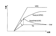
となる。上記dは4ビットの制御信号in<0>〜in<3>をin<0>が最下位ビット、in<3>が最上位ビットの2進数としてみた場合の値であり、例えばin<3>,in<2>,in<1>,in<0>が(”0”,”0”,”0”,”0”)ならば、d=0であり、RN=0Ωとなる。また、例えばin<3>,in<2>,in<1>,in<0>が(”0”,”1”,”1”,”1”)ならば、d=7であり、RN=1.25MΩ*7=8.25MΩとなる。従って、図1の回路ではVoutとして、(0.5+0.125*d)Vの電圧が出力される。つまりVoutは0.5Vから2.375Vの範囲で0.125Vステップで調整することができる。
【0048】
ここで、同じ4ビットの制御信号に応じて出力電圧の値が調整される図16の従来回路と図1の回路における抵抗の数を比較する。図1の回路では図3に示す可変抵抗回路12で4個の抵抗が使用されているので、抵抗の数は全部で5個である。これに対して、図16の従来回路では15個の抵抗が使用されている。
【0049】
このように第1の実施の形態によるものでは、従来回路に比べて使用される抵抗の数を削減することができる。一般に、図4に示すように拡散層抵抗などによって構成される高抵抗は、トランジスタなどと比べてチップ上で大きな面積を占めるので、抵抗の数が減れば全体の回路面積を削減することができる。
【0050】
また、第1の実施の形態によるものでは、オペアンプを含むフィードバック回路が1系統しか設けられていないので、素子の製造上のばらつきに対して強くなり、回路動作の安定性を図ることができる。
【0051】
また、可変抵抗回路12として図3に示すような構成のものを用いたことにより、フィードバック回路の応答性が向上するという効果が得られる。すなわち、可変抵抗回路12では高抵抗が用いられており、後述するが、このような高抵抗は比較的大きな寄生容量を有している。図3に示す可変抵抗回路12では、選択された抵抗のみがVoutのノードと抵抗13との間に接続されるようになり、非選択の抵抗は接地電圧VSSのノードに接続される。すなわち、余分な抵抗は分離し、接地されるので、余分な寄生容量成分を切り離すことができ、フィードバック回路の応答性が向上する。
【0052】
なお、上記実施の形態において、可変抵抗回路12には4個の抵抗31〜39を設け、これら4個の抵抗を4ビットの制御信号in<0>〜in<3>に基づいて選択する場合について説明したが、これは可変抵抗回路12内に4個以上または3個以下の抵抗を設けるようにしてもよい。4個以上の抵抗を設けた場合には、それに応じて制御信号のビット数を増加させ、かつ図3に示される可変抵抗回路12の構成も変える必要があるが、要するに抵抗とスイッチ回路とが交互に接続されるように複数の抵抗とスイッチ回路とを接続し、制御信号に応じて選択される抵抗が出力電圧Voutのノードと抵抗13の一端との間に直列接続され、非選択の抵抗は直列接続され、その直列接続された一端の抵抗の一端と他端の抵抗の一端とが共に接地電圧VSSのノードに接続されるように可変抵抗回路12を構成すればよい。
【0053】
<第2の実施の形態>
図8は、この発明の第2の実施の形態による、電源回路を有する半導体集積回路の構成を示している。
【0054】
この実施の形態による回路は、図1のものに対して新たに2個のNMOSトランジスタ15、16が追加されている。NMOSトランジスタ15のドレイン・ソース間は、PMOSトランジスタ11のドレインと可変抵抗回路12の一端との間に挿入され、ゲートはドレインに接続されている。NMOSトランジスタ16のゲートはNMOSトランジスタ15のゲートと共通に接続され、NMOSトランジスタ16のドレイン・ソース間は、VDDとは異なる電源電圧VDD2の供給ノードと電圧Voutのノードに接続されている。
【0055】
ここで、新たに追加された2個のトランジスタ15、16はカレントミラー回路を構成しており、可変抵抗回路12に流れる電流に比例した電流がトランジスタ16に流れ、Voutのノードからは可変抵抗回路12の一端、つまりトランジスタ15のソース側に発生する電圧と等しい電圧が出力される。
【0056】
この実施の形態による回路では、図1のものと同様に、回路面積を削減することができる、素子の製造上のばらつきに対して強くなり、回路動作の安定性を図ることができる、という効果が得られる上に、さらに以下のような効果も得ることができる。
【0057】
すなわち、この実施の形態による回路では、ドレインが電源電圧VDD2の供給ノードに接続されたNMOSトランジスタ16を介して出力電圧Voutが取り出されるので、Voutにかかる負荷の変動に対して、Voutの電位変動が小さくなるように設計することができる。つまり負荷に応じてNMOSトランジスタ16のチャネル幅を変えることにより、Voutの電位変動を小さく押さえることができる。
【0058】
なお、上記電源電圧VDD2は電源電圧VDDと等しい電圧にしてもよい。
【0059】
ところで、上記第1、第2の実施の形態による回路では、抵抗として1MΩ以上の高抵抗を用いているので消費電力を少なくすることができる半面、電源立ち上げ時の出力電圧Voutの確定時間が比較的長くなる。以下にこれについて説明する。
【0060】
先の抵抗13に流れる電流Iは例えば0.1μAと非常に小さく、これにより超低消費電流が実現されるが、このような超低消費電流を達成するために使用される抵抗として1MΩ以上の高抵抗が用いられる。集積回路では、このような高抵抗として、先の図4に示されるような拡散層抵抗が用いられる。拡散層はそれが形成されている半導体領域(基板あるいはウェル領域など)に対して寄生容量を持つため、拡散層抵抗は抵抗*寄生容量なる時定数を持つ。寄生容量の代表的な値は、例えば1MΩ当たり0.3pFである。従って、5MΩの抵抗の時定数は、5MΩ*1.5pF=7.5μsとなり、20MΩの場合は20MΩ*6pF=120μs程度となる。
【0061】
従って、図1や図8に示される実施の形態回路の時定数は概ね100μs以上となり、電源投入後から数100μs程度の期間では出力電位が安定しない。ただし、一度、出力電位が安定してしまえば、回路の時定数が100μs以上であっても、フィードバック回路の増幅特性によって出力電位が安定することが知られている。
【0062】
しかしながら、電源投入直後は、出力電位が確定するまでの時間として、高抵抗に加わる電位が定常状態になるまでに、抵抗値と容量とで決まる時定数がかかるため、数100μs以上の時間がかかってしまう。
【0063】
半導体集積回路の多くは、電源投入直後動作可能となるまでの時間を定格値として規定しているが、その値は例えばシンクロナスDRAMでは200μsであり、数100μs以上の安定化時間を取ることができない。これを回避する1つの方法は、抵抗値を低くすることによって短い時定数を実現することであるが、これでは消費電力が大きくなってしまう。
【0064】
そこで次に、高抵抗を用いて超低消費電流を実現すると共に、電源投入直後に出力電圧が早く確定するようにした種々の実施の形態について説明する。
【0065】
<第3の実施の形態>
図9は、この発明の第3の実施の形態による、電源回路を有する半導体集積回路の構成を示している。
【0066】
この実施の形態による回路は、Voutのノードと可変抵抗回路12の他端との間に容量17が接続されている点が図1のものとは異なる。
【0067】
上記容量17は、Voutのノードにおける電位変動を可変抵抗回路12と抵抗13との直列接続ノードである電圧Vaのノードに素早く伝え、出力電圧Voutのノードの電位をオペアンプ14に早く帰還させる機能を持つ。
【0068】
図10は、電源投入時における電源電圧VDD、出力電圧Vout及び電圧Vaそれぞれのノードにおける電位変化の状態を示す波形図である。
【0069】
次に、図10を参照して図9の回路の動作を説明する。
【0070】
電源が投入されると、電源電位VDDは0Vから急激に上昇する。これに伴い、PMOSトランジスタ11を介して出力電圧Voutのノードが充電され、Voutのノードの電位も上昇する。ここで、容量17によりVoutのノードとVaのノードとが容量結合されているので、Voutのノードの電位上昇に伴ってVaのノードの電位も上昇する。Vaのノードはオペアンプ14の非反転入力端子(+)に接続されているので、Vaのノードの電位が基準電位Vrefよりも高くなると、オペアンプ14の出力が“H”となり、PMOSトランジスタ11がオフ状態になる。これによってVoutのノードの電位の上昇が止められる。
【0071】
この後は、先に説明したように、フィードバック回路の働きにより、Voutのノードの電位が下がることによってVaの電位が下がり、PMOSトランジスタ11がオン状態になることによってVoutのノードの電位が上昇し、逆にVoutのノードの電位が上がることによってVaの電位が上がり、PMOSトランジスタ11がオフ状態になることによってVoutのノードの電位の上昇が止まることにより、Voutのノードの電位が一定値に制御される。
【0072】
図10中、破線で示したVoutとVaのノードの電位変化は、上記容量17を設けていない場合である。この場合、電源投入直後にVoutのノードの電位が急激に上昇するのに対して、Vaのノードの電位は穏やかに上昇する。このような現象が起こる理由は、抵抗13が非常に大きな抵抗値と寄生容量とを持ち、Voutのノードの電位がVaのノードに影響を与える際に、抵抗13の抵抗値と寄生容量との積で表される時定数分程度の遅延が生じるためである。このため、電位Vaはなかなか基準電圧Vrefに到達せず、従って、Voutが所望の値より上昇しすぎてオーバーシュートを起こしてしまう。
【0073】
第3の実施の形態によるものでは、容量17によってVoutのノードとVaのノードを容量結合させているので、電源投入直後の動作を安定させることができ、電源投入直後に出力電位を早く確定させることができる。
【0074】
なお、図9中の実施の形態回路における可変抵抗12としては、図3に示した構成の回路の他に、例えば図12(a)〜(c)に示すような構成のものを使用することができる。
【0075】
図12(a)に示される可変抵抗12は、4個の抵抗31〜34と、これらの各抵抗31〜34に対して並列に接続されたスイッチとしての4個のNMOSトランジスタ71と、4ビットの制御信号in<0>〜in<3>のそれぞれが入力される4個のインバータ72とから構成されている。そして、制御信号in<0>〜in<3>が4個のインバータ72でそれぞれ反転されて4個のNMOSトランジスタ71の各ゲートに入力される。4個の抵抗31〜34の各抵抗値は、図3中のものと同じである。
【0076】
図12(a)の可変抵抗12において、4ビットの制御信号in<0>〜in<3>の全てが“0”であれば、4個のインバータ72の出力は全て“1”となり、4個のNMOSトランジスタ71の全てがオン状態になる。この場合、4個の抵抗31〜34はそれぞれの両端が短絡されるので、可変抵抗12の抵抗値は0になる。
【0077】
そして、例えばin<0>のみが“1”の場合には、この制御信号が入力されるインバータ72の出力が“0”となり、このインバータ72の出力がゲートに入力されるNMOSトランジスタ71のみがオフ状態となる。従って、この場合には可変抵抗12の両端間には抵抗31のみが接続された状態となり、可変抵抗12における抵抗値は抵抗31の抵抗値となる。
【0078】
また、例えばin<0>〜in<3>の全てが“1”であれば、4個のインバータ72の出力が全て“0”となり、4個のNMOSトランジスタ71の全てがオフ状態となる。従って、この場合には可変抵抗12の両端間には抵抗31〜34が直列接続された状態となり、可変抵抗12における抵抗値は抵抗31〜34の直列抵抗値となる。
【0079】
図12(b)に示される可変抵抗12は、各抵抗の両端を短絡するまたは解放するスイッチとして、図12(a)中のNMOSトランジスタ71の代わりにPMOSトランジスタ73を使用するようにしたものである。この場合にはインバータ72は不要である。
【0080】
図12(c)に示される可変抵抗12は、各抵抗の両端を短絡するまたは解放するスイッチとして、図12(a)中のNMOSトランジスタ71と図12(b)中のPMOSトランジスタ73とを組み合わせて使用するようにしたものである。
【0081】
なお、図12(a)〜(c)に示すような構成の可変抵抗12においても、抵抗の数は4個に限定されるものではなく、4個以上設けるようにしてもよい。
【0082】
ところで、図9の実施の形態回路では、容量17の値については特に説明しなかったが、この容量17の値としては、図3及び図12(a)〜(c)に示すような構成の可変抵抗回路12を用いて、出力電圧Voutの値が調整可能な0.5Vから2.375Vの間のほぼ中間の電圧をVoutの所望値とした場合に、電源投入直後の出力電圧が最も早く安定するような値が選ばれる。容量17の値を上記のような値に選べば、電源投入直後に出力電圧Voutは図10中の実線で示すように変化する。
【0083】
ところが、容量17をこのような値に固定して、出力電圧Voutが例えば0.5Vになる設定を選択すると、図11の波形図に示すように出力電圧Voutの波形がオーバーシュートを起こしてしまう。また逆に出力電圧Voutの設定値が例えば2.375Vの場合には、PMOSトランジスタ11がオフ状態にされるまでの時間が早すぎて、図11の波形図に示すように出力電圧Voutがなかなか設定値に到達しなくなる。
【0084】
従って、一定値の容量ではなく、出力電圧Voutの値に応じて容量値が変化する容量回路を用いてVoutのノードとVaのノードとを容量結合させるようにすれば、設定された出力電圧Voutに応じて早く確定させることができるようになる。
【0085】
<第4の実施の形態>
図13は、この発明の第4の実施の形態による、電源回路を有する半導体集積回路の構成を示している。
【0086】
この実施の形態による回路は、図9の実施の形態回路における一定の値の容量17に換えて、出力電圧Voutの値に応じて容量値が変化する容量回路18をVoutのノードとVaのノードとの間に接続するようにしたものである。
【0087】
なお、この場合、可変抵抗回路12としては図12(a)に示すような構成のものを使用している。ただし、図12(a)中のインバータ72は図示を省略している。
【0088】
容量回路18は、出力電圧Voutのノードと可変抵抗回路12の他端との間に接続された容量81と、Voutのノードと可変抵抗回路12の他端との間に接続され、NMOSトランジスタ82と容量83とを直列接続した直列回路84と、Voutのノードと可変抵抗回路12の他端との間に接続され、NMOSトランジスタ85と容量86とを直列接続した直列回路87とから構成されている。そして、上記NMOSトランジスタ82のゲートには制御信号in<2>の反転信号/in<2>が入力され、NMOSトランジスタ85のゲートには制御信号in<3>の反転信号/in<3>が入力される。
【0089】
なお、可変抵抗回路12の他端(電圧Vaのノード)と接地電圧VSSの供給ノードとの間には、電圧Vaの安定化を図るために安定化容量88が接続されている。
【0090】
このような構成において、4ビットの制御信号in<0>〜in<3>の全てが“0”であり、可変抵抗回路12内の全てのNMOSトランジスタ71がオン状態にされて、最も低い値に設定されたVoutが出力される場合を考える。この場合、容量回路18内の直列回路84、87におけるNMOSトランジスタ82、85がオン状態になるので、容量回路18における容量値は3個の容量81、83及び86の並列容量値となり、容量回路18が取り得る最も大きな容量値となる。
【0091】
従って、この場合には、電源投入直後にVoutのノードの電位が上昇とすると、Vaのノードの電位が急激に上昇し、オペアンプ14の出力によってPMOSトランジスタ11がオフ状態にされるのが電源投入後、相対的に早くなる。従って、PMOSトランジスタ11を介したVoutのノードの充電が早く止まり、Voutのノードの余分な電位上昇は生じない。すなわち、図11に示されるような電源投入直後にオーバーシュートを起こしていた現象が解消され、Voutは設定された値に早く確定する。
【0092】
次に、4ビットの制御信号in<0>〜in<3>のうちin<2>とin<3>が“1”であり、可変抵抗回路12内で比較的高い値を持つ抵抗34、33がVoutのノードとVaのノードとの間に直列に接続され、Voutのノードからは比較的高い電圧が出力される場合を考える。この場合、容量回路18内の直列回路84、85におけるNMOSトランジスタ82、85は共にオフ状態になり、容量回路18における容量値は1個の容量81の値と等しくなる。この場合、4ビットの制御信号in<0>〜in<3>の全てが“0”の場合と比べ、容量回路18における容量値は減少する。従って、この場合には、VoutのノードとVaのノードとの間の容量結合の程度が減少し、Voutのノードの電位が上昇してもVaのノードの電位はそれ程上昇しない。
【0093】
そして、オペアンプ14の出力によってPMOSトランジスタ11がオフ状態にされるのが電源投入後、相対的に遅くなり、PMOSトランジスタ11を介したVoutのノードの充電が長く行われるので、Voutの初期電位が高くなる。すなわち、図11に示したような電源投入直後にVoutがなかなか上昇しない現象は解消され、Voutは設定された値に早く確定する。
【0094】
なお、この実施の形態では、容量回路18内にNMOSトランジスタと容量とを直列接続した直列回路が2個設けられているので、出力電圧Voutの値が最も高いときと最も低いときの間が4段階に分けられ、それに対応して容量回路18における容量値が変化するようになる。出力電圧Voutの値は、可変抵抗回路12内に設けられている4個の抵抗31〜34のうち抵抗値が高い抵抗によって大きく影響されるので、この実施の形態では最も抵抗値が高い抵抗34と次に抵抗値が高い抵抗33に対応して容量回路18内に直列回路を設けるようにしている。しかし、それ程影響がない場合には、最も抵抗値が高い抵抗34に対応して容量回路18内に直列回路を1個設けるようにしてもよく、あるいはより高精度に制御する必要がある場合には2個以上の直列回路を設けるようにしてよい。
【0095】
<第5の実施の形態>
図14は、この発明の第5の実施の形態による、電源回路を有する半導体集積回路の構成を示している。
【0096】
図13の実施の形態で説明したように、出力電圧Voutの設定値が高い場合にはVoutのノードとVaのノードとの間の容量結合を弱くし、設定値が低い場合には強くすることによって、電源投入後にVoutを所望の値に早く確定させることができる。そして、図13の実施の形態では、VoutのノードとVaのノードとの間の容量結合の度合いを、VoutのノードとVaのノードとの間に接続される容量値を変えることで実現している。
【0097】
しかし、VoutのノードとVaのノードとの間の容量結合の度合いは、Vaのノードに接続される安定化容量と、VoutのノードとVaのノードとの間に接続される容量との比によっても決まる。
【0098】
そこで、図14に示した実施の形態回路では、VoutのノードとVaのノードの間には容量81のみを接続し、Vaのノードと接地電圧VSSのノードとの間に接続される容量の値を変えるようにしたものである。
【0099】
図14中の容量回路18は、VoutのノードとVaのノードの間に接続された容量81と、Vaのノードと接地電圧VSSのノードとの間に接続された安定化容量88と、Vaのノードと接地電圧VSSのノードとの間に接続され、NMOSトランジスタ89と容量90とを直列接続した直列回路91と、Vaのノードと接地電圧VSSのノードとの間に接続され、NMOSトランジスタ92と容量93とを直列接続した直列回路94とから構成されている。そして、上記NMOSトランジスタ89のゲートには制御信号in<2>が入力され、NMOSトランジスタ92のゲートには制御信号in<3>が入力される。
【0100】
このような構成において、4ビットの制御信号in<0>〜in<3>の全てが“1”であり、可変抵抗回路12内の全てのNMOSトランジスタ71がオフ状態にされて、最も高い値に設定されたVoutが出力される場合を考える。この場合、容量回路18内の直列回路91、94におけるNMOSトランジスタ89、92はオン状態になるので、Vaのノードと接地電圧VSSのノードとの間には3個の容量81、90、93が接続され、Vaのノードと接地電圧VSSのノードとの間の容量値が大きくなる。
【0101】
従って、この場合には、Voutのノードの電位が上昇してもVaのノードの電位はそれ程上昇しない。そして、オペアンプ14の出力によってPMOSトランジスタ11がオフ状態にされるのが電源投入後、相対的に遅くなり、PMOSトランジスタ11を介したVoutのノードの充電が長く行われるので、Voutの初期電位が高くなる。すなわち、電源投入直後にVoutがなかなか上昇しない現象は解消され、Voutは設定された値に早く確定する。
【0102】
4ビットの制御信号in<0>〜in<3>のうちin<2>あるいはin<3>が“0”であり、Voutのノードから比較的低い電圧が出力される場合には、直列回路91、94におけるNMOSトランジスタ89あるいは92がオフ状態になり、Vaのノードと接地電圧VSSのノードとの間の容量値は先の場合よりも小さくなる。このような場合にはVoutのノードとVaのノードとの間に接続されている容量81による容量結合の効果が強まる。つまり、電源投入直後にVoutのノードの電位が上昇とすると、Vaのノードの電位が急速に上昇し、オペアンプ14の出力によってPMOSトランジスタ11がオフ状態にされるのが電源投入後、相対的に早くなる。従って、PMOSトランジスタ11を介したVoutのノードの充電が早く止まり、Voutのノードの余分な電位上昇は生じない。すなわち、電源投入直後にオーバーシュートは起きなくなり、Voutは設定された値に早く確定する。
【0103】
なお、この実施の形態では、容量回路18内にNMOSトランジスタと容量とを直列接続した直列回路が2個設けられているので、出力電圧Voutの値が最も高いときと最も低いときの間が4段階に分けられ、それに対応して容量回路18におけるVaのノードとVSSのノードとの間の容量値が変化するようになる。出力電圧Voutの値は、可変抵抗回路12内に設けられている4個の抵抗31〜34のうち抵抗値が高い抵抗によって大きく影響されるので、この実施の形態では最も抵抗値が高い抵抗34と次に抵抗値が高い抵抗33に対応して容量回路18内に直列回路を設けるようにしている。しかし、それ程影響がない場合には、最も抵抗値が高い抵抗34に対応して容量回路18内に直列回路を1個設けるようにしてもよく、あるいはより高精度に制御する必要がある場合には2個以上の直列回路を設けるようにしてよい。
【0104】
<第6の実施の形態>
図15は、この発明の第6の実施の形態による、電源回路を有する半導体集積回路の構成を示している。
【0105】
先の図9の実施の形態では、電源投入後にVoutを所望の値に早く確定させるために、VoutのノードとVaのノードとの間に容量17を接続して両ノード間を容量結合させるようにしている。
【0106】
これに対して、図15の実施の形態回路では、VoutのノードとVaのノードとの間に容量回路18を設けることで、設定された出力電圧Voutに応じてVoutを早く確定させると共に、可変抵抗回路12の中間ノードに存在している寄生容量を早く充電して、Voutを所望の値に早く確定させる効果を高めるようにしている。
【0107】
すなわち、この実施の形態回路に設けられている容量回路18は、VoutのノードとVaのノードとの間に接続された容量81と、Voutのノードと可変抵抗回路12の中間ノード、例えば図15では最も抵抗値が大きい抵抗34と次に抵抗値が大きい抵抗33の直列接続ノードとの間に接続された容量95と、Voutのノードと上記両抵抗34、抵抗33の直列接続ノードとの間に接続され、NMOSトランジスタ96と容量97とを直列接続した直列回路98とから構成されている。なお、上記トランジスタ96のゲートには制御信号in<2>が入力される。
【0108】
この実施の形態回路において、容量95は、可変抵抗回路12の中間ノードのうち最も抵抗値が大きい抵抗34と次に抵抗値が大きい抵抗33の直列接続ノードに存在している寄生容量を、Voutのノードの電位に応じて充電するためのものである。
【0109】
なお、抵抗34が選択されるか否かによって、抵抗34と抵抗33の直列接続ノードの電位を持ち上げる量が違ってくるので、NMOSトランジスタ96と容量97とからなる直列回路98を設け、抵抗34が選択される時にはNMOSトランジスタ96をオンさせて、容量96を介して、抵抗34と抵抗33の直列接続ノードに存在している寄生容量を充電する。
【0110】
この実施の形態では、電源投入直後にVoutのノードの電位が上昇とすると、容量81を介した経路により、Vaのノードの電位が影響を受けて、Vaのノードの電位が急激に上昇し、オペアンプ14の出力によってPMOSトランジスタ11がオフ状態にされるのが電源投入後、相対的に早くなる。従って、PMOSトランジスタ11を介したVoutのノードの充電が早く止まり、Voutのノードの余分な電位上昇は生じなくなり、Voutは設定された値に早く確定する。
【0111】
また、これと同時に容量95または容量95と96による経路により、抵抗34と抵抗33の直列接続ノードに存在している寄生容量が充電され、Voutが設定された値に確定する速度が速くなる。
【0112】
なお、上記図13ないし図15の各実施の形態回路では、可変抵抗回路12として図12(a)に示すような構成のものを用いる場合について説明したが、これは図12(b)、(c)に示すような構成のもの、あるいは図3に示すような構成のものを使用するようにしてもよい。また、可変抵抗回路12に設けられる抵抗の数も4個に限定されるものではなく4個以上又は3個以下の数だけ設けるような構成としてもよい。
【0113】
さらに、上記図13ないし図15の各実施の形態の変形例として、図8の実施の形態のように、NMOSトランジスタ15、16からなるカレントミラー回路を設ける構成としてもよい。カレントミラー回路を設ける場合、容量17や容量回路18は、NMOSトランジスタ15のソースのノードとVaのノードとに接続する。そして、このカレントミラー回路を設けることで、図8の実施の形態の場合と同様に、Voutの電位変動を小さく押さえることができる。
【0114】
第4乃至第6の実施の形態では、第1乃至第3の実施の形態回路と同様に、面積を削減することができる、素子の製造上のばらつきに対して強くなり回路動作の安定性を図ることができる、という効果が得られる上に、さらに、電源投入直後にVoutのノードの電位を設定された値に早く確定させることができ、高速起動が実現できるという効果が得られる。
【0115】
【発明の効果】
以上説明したようにこの発明によれば、回路面積の削減を図ることができると共に安定した回路動作を得ることができる電源回路を有する半導体集積回路を提供することができる。
【図面の簡単な説明】
【図1】この発明の第1の実施の形態による電源回路を有する半導体集積回路の構成を示す回路図。
【図2】図1中のオペアンプの具体的な構成例を示す回路図。
【図3】図1で使用される可変抵抗回路の具体的な構成例を示す回路図。
【図4】図1中の抵抗の素子構造を示す断面図。
【図5】図3中のスイッチ回路を抜き出して内部接続状態を示す図。
【図6】図3中のスイッチ回路の具体的な構成の一例を示す回路図。
【図7】図3の可変抵抗回路の内部接続状態の変化を示す回路図。
【図8】この発明の第2の実施の形態による電源回路を有する半導体集積回路の構成を示す回路図。
【図9】この発明の第3の実施の形態による電源回路を有する半導体集積回路の構成を示す回路図。
【図10】図9の回路の電源投入時における各ノードの電位変化の状態を示す波形図。
【図11】図9の回路をある条件で動作させた時の電源投入時における各ノードの電位変化の状態を示す波形図。
【図12】図9中の実施の形態回路における可変抵抗の他の構成例を示す回路図。
【図13】この発明の第4の実施の形態による電源回路を有する半導体集積回路の構成を示す回路図。
【図14】この発明の第5の実施の形態による電源回路を有する半導体集積回路の構成を示す回路図。
【図15】この発明の第6の実施の形態による電源回路を有する半導体集積回路の構成を示す回路図。
【図16】従来の電源回路の一例を示す回路図。
【符号の説明】
11…PMOSトランジスタ、
12…可変抵抗回路、
13、31〜34…抵抗、
14…オペアンプ、
15、16…NMOSトランジスタ、
17…容量、
18…容量回路、
35〜39…スイッチ回路。[0001]
BACKGROUND OF THE INVENTION
The present invention relates to a semiconductor integrated circuit having a power supply circuit in which a value of an output voltage is adjusted according to a control signal.
[0002]
[Prior art]
Semiconductor integrated circuits, particularly power supply circuits provided in semiconductor memory products, have diversified set voltages. In particular, in a power supply circuit used in a dynamic memory or a ferroelectric memory, it is necessary to output various voltages between the external power supply voltage VDD and the ground voltage VSS. However, the optimum setting value of this voltage may differ depending on the characteristics of the memory cell after processing. For this reason, the output voltage of a power supply circuit is adjusted by the operation test after a process.
[0003]
An example of a conventional power supply circuit capable of adjusting the output voltage is shown in FIG. This power supply circuit is composed of a resistance ladder circuit composed of a plurality of resistors r and two systems of feedback circuits using operational amplifiers.
[0004]
In the circuit of FIG. 16, due to the characteristics of the feedback circuit using the operational amplifier, the voltage Vx at the non-inverting input terminal (+) of one
[0005]
Then, by changing the distribution of the currents ix and iy based on the control signals in <0> to in <3>, the connection is made between the node of the output voltage Vout and the non-inverting input terminal (+) of one
[0006]
For example, if the control signal is a 4-bit signal as shown in FIG. Four = Current distribution can be changed in 16 steps. That is, the value of the current ix is (Vref / r) * (d / 16) (where d is an integer from 0 to 15), and the output voltage Vout is expressed by Vref + R * ix, so that there are 16 voltages as Vout. Can be set.
[0007]
However, since many resistors are used in the conventional circuit shown in FIG. 16, there is a problem that the circuit area increases.
[0008]
In addition, since a plurality of feedback circuits (two systems in FIG. 16) are used, the circuit is vulnerable to variations in device manufacturing, and there is a problem in the stability of circuit operation.
[0009]
[Problems to be solved by the invention]
As described above, the conventional power supply circuit has a problem that the circuit area increases because a large number of resistors are used. Also, since a plurality of feedback circuits are used, the circuit is weak against variations in device manufacturing. There is a problem with the stability of operation.
[0010]
The present invention has been made in view of the above circumstances, and an object of the present invention is to provide a semiconductor integrated circuit having a power supply circuit capable of reducing the circuit area and obtaining a stable circuit operation. It is to be.
[0011]
[Means for Solving the Problems]
A semiconductor integrated circuit according to an embodiment of the present invention includes a transistor in which one end of a current path is connected to a first voltage supply node and the other end of the current path is connected to a voltage output node; One end connected to the voltage output node, a plurality of first resistors, and the other end, and the resistance value changes according to the control signal Variable resistance circuit and the other end of the variable resistance circuit And second The second resistor connected between the two voltage supply nodes and the voltage at the other end of the variable resistance circuit are compared with a reference voltage, and a signal corresponding to the comparison result is fed back to the gate of the transistor. Comparison circuit
And The plurality of first resistors are each composed of a diffusion layer resistor, the first resistor is selected according to the control signal, and the selected first resistor is connected to one end of the variable resistor circuit and the variable resistor. Connected in series with the other end of the resistor circuit, and the non-selected first resistor is connected to the second voltage supply node. It is characterized by that.
[0012]
A semiconductor integrated circuit according to another embodiment of the present invention includes a first transistor having a first polarity in which one end of a current path is connected to a first voltage supply node, and one end of the current path and a gate are connected to the first transistor. A second transistor of the second polarity connected to the other end of the current path of the transistor; One end connected to the other end of the current path of the second transistor, a plurality of first resistors, and the other end, and the resistance value changes according to the control signal Variable resistance circuit and the other end of the variable resistance circuit And second The second resistor connected between the two voltage supply nodes and the voltage at the other end of the variable resistance circuit are compared with a reference voltage, and a signal corresponding to the comparison result is output to the gate of the first transistor. A third feedback circuit having a gate connected to the gate of the second transistor and a current path connected between a third voltage supply node and a voltage output node; Equipped with The plurality of first resistors are each composed of a diffusion layer resistor, the first resistor is selected according to the control signal, and the selected first resistor is connected to one end of the variable resistor circuit and the variable resistor. Connected in series with the other end of the resistor circuit, and the non-selected first resistor is connected to the second voltage supply node. It is characterized by that.
[0013]
DETAILED DESCRIPTION OF THE INVENTION
Hereinafter, the present invention will be described in detail with reference to the drawings.
[0014]
<First Embodiment>
FIG. 1 shows the configuration of a semiconductor integrated circuit having a power supply circuit according to the first embodiment of the present invention.
[0015]
The source of the
[0016]
In such a configuration, the voltage Va at the non-inverting input terminal (+) of the
[0017]
FIG. 2 shows a specific circuit configuration example of the
[0018]
The
[0019]
In the
[0020]
On the contrary, when the voltage Va drops below the reference voltage Vref, the current flowing through the
[0021]
When the
[0022]
Contrary to the above, when the voltage Va falls below the reference voltage Vref, the current flowing through the
[0023]
By such an operation, as described above, the voltage Va at the non-inverting input terminal (+) of the
[0024]
Here, for example, when the value of the reference voltage Vref is set to 0.5 V and the resistance value of the
[0025]
FIG. 3 shows a specific circuit configuration example of the
[0026]
Each of the
[0027]
The input / output terminal B of the
[0028]
The decoder circuit is a 4-bit control signal in <0> to in Control signals to be input to the control input terminals S of the
[0029]
[0030]
The exclusive OR
[0031]
The exclusive OR
[0032]
The exclusive OR
[0033]
[0034]
FIG. 4 shows element cross-sectional structures of the
[0035]
FIG. 5A shows one of the switch circuits in FIG. When the control signal in supplied to the control input terminal S of the switch circuit is “0”, as shown in FIG. 5B, each switch circuit is connected between the input / output terminals A and B and the input / output terminals C and D. Are controlled to be connected to each other. On the other hand, when the control signal in supplied to the control input terminal S of the switch circuit is “1”, each switch circuit is connected between the input / output terminals A and C and the input / output terminals as shown in FIG. Control is performed so that B and D are connected to each other.
[0036]
An example of a specific configuration of the switch circuit having such a function is shown in FIG.
[0037]
This switch circuit is composed of four
[0038]
In the configuration as shown in FIG. 6, when a signal “0” is supplied to the control input terminal S, the output of the
[0039]
When a signal “1” is supplied to the control input terminal S, the
[0040]
Here, the resistance values of the four
[0041]
Further, of the four
[0042]
In the
[0043]
For example, as shown in FIG. 7A, a 4-bit control signal in <0> to in When <3> is all “0”, the control signals input to the control input terminals S of the
[0044]
As shown in FIG. 7B, a 4-bit control signal in <0> to in In <3> Only <0> is “1” and the remaining in <1> to in When <3> is all “0”, the control signals input to the control input terminals S of the
[0045]
FIG. 7C shows a 4-bit control signal in <0> to in In <3> When only <1> is “1” and the rest are all “0”, the control signal input to the control input terminal S of the
[0046]
Similarly, FIG. 7D shows a 4-bit control signal in <0> to in In <3> FIG. 7E shows the connection state of each resistor when only <0> is “0” and the rest are all “1”. FIG. <0> to in The connection state of each resistor when all of <3> is “1” is shown. The resistance value between the Vout node and the
[0047]
Thus, in the
RN = 1.25 MΩ * d (where d is an integer in the range of 0 to 15)
It becomes. D is a 4-bit control signal in <0> to in <3> in <0> is the least significant bit, in <3> is the value when viewed as the most significant binary number, for example in <3>, in <2>, in <1>, in If <0> is (“0”, “0”, “0”, “0”), d = 0 and RN = 0Ω. For example, in <3>, in <2>, in <1>, in If <0> is (“0”, “1”, “1”, “1”), d = 7 and RN = 1.25 MΩ * 7 = 8.25 MΩ. Therefore, in the circuit of FIG. 1, a voltage of (0.5 + 0.125 * d) V is output as Vout. That is, Vout can be adjusted in the range of 0.5V to 2.375V in 0.125V steps.
[0048]
Here, the number of resistors in the conventional circuit of FIG. 16 in which the value of the output voltage is adjusted according to the same 4-bit control signal and the circuit of FIG. 1 are compared. In the circuit of FIG. 1, since the four resistors are used in the
[0049]
As described above, according to the first embodiment, the number of resistors used can be reduced as compared with the conventional circuit. In general, as shown in FIG. 4, a high resistance constituted by a diffusion layer resistance occupies a large area on a chip as compared with a transistor or the like, so that the entire circuit area can be reduced if the number of resistors is reduced. .
[0050]
Further, according to the first embodiment, since only one system of feedback circuits including an operational amplifier is provided, it is strong against variations in device manufacturing, and circuit operation stability can be achieved.
[0051]
Further, the use of the
[0052]
In the above embodiment, the
[0053]
<Second Embodiment>
FIG. 8 shows a configuration of a semiconductor integrated circuit having a power supply circuit according to the second embodiment of the present invention.
[0054]
In the circuit according to this embodiment, two
[0055]
Here, the two newly added
[0056]
In the circuit according to this embodiment, as in the case of FIG. 1, it is possible to reduce the circuit area, to be strong against variations in manufacturing of elements, and to achieve stability of circuit operation. As well as the following effects.
[0057]
That is, in the circuit according to this embodiment, since the output voltage Vout is taken out through the
[0058]
The power supply voltage VDD2 may be equal to the power supply voltage VDD.
[0059]
By the way, in the circuits according to the first and second embodiments, a high resistance of 1 MΩ or more is used as the resistance, so that the power consumption can be reduced. On the other hand, the determination time of the output voltage Vout at the time of starting the power supply is reduced. Relatively long. This will be described below.
[0060]
The current I flowing through the
[0061]
Accordingly, the time constant of the embodiment circuit shown in FIGS. 1 and 8 is approximately 100 μs or more, and the output potential is not stable in a period of several hundred μs after the power is turned on. However, it is known that once the output potential is stabilized, the output potential is stabilized by the amplification characteristics of the feedback circuit even if the time constant of the circuit is 100 μs or more.
[0062]
However, immediately after the power is turned on, it takes a time of several hundreds of microseconds or more since the time constant determined by the resistance value and the capacitance is required until the potential applied to the high resistance reaches a steady state as the time until the output potential is determined. End up.
[0063]
In many semiconductor integrated circuits, the time until operation is possible immediately after power-on is defined as a rated value, which is, for example, 200 μs for a synchronous DRAM and may take a stabilization time of several hundreds μs or more. Can not. One way to avoid this is to achieve a short time constant by lowering the resistance value, but this increases power consumption.
[0064]
Next, various embodiments in which ultra-low current consumption is realized using a high resistance and the output voltage is determined quickly immediately after the power is turned on will be described.
[0065]
<Third Embodiment>
FIG. 9 shows a configuration of a semiconductor integrated circuit having a power supply circuit according to the third embodiment of the present invention.
[0066]
The circuit according to this embodiment differs from that of FIG. 1 in that a
[0067]
The
[0068]
FIG. 10 is a waveform diagram showing the state of potential change at each node of the power supply voltage VDD, the output voltage Vout, and the voltage Va when the power is turned on.
[0069]
Next, the operation of the circuit of FIG. 9 will be described with reference to FIG.
[0070]
When the power is turned on, the power supply potential VDD rises rapidly from 0V. Along with this, the node of the output voltage Vout is charged through the
[0071]
Thereafter, as described above, the potential of the node Vout decreases as the potential of the node Vout decreases due to the action of the feedback circuit, and the potential of the node Vout increases as the
[0072]
In FIG. 10, potential changes at the nodes Vout and Va indicated by broken lines are when the
[0073]
In the third embodiment, since the Vout node and the Va node are capacitively coupled by the
[0074]
In addition to the circuit having the configuration shown in FIG. 3, for example, a
[0075]
The
[0076]
In the
[0077]
And for example in When only <0> is “1”, the output of the
[0078]
For example, in <0> to in If all of <3> are “1”, the outputs of the four
[0079]
The
[0080]
The
[0081]
In the
[0082]
In the circuit of the embodiment shown in FIG. 9, the value of the
[0083]
However, if the
[0084]
Therefore, if the Vout node and the Va node are capacitively coupled using a capacitance circuit whose capacitance value changes according to the value of the output voltage Vout instead of a constant capacitance, the set output voltage Vout is set. It will be possible to make a decision quickly according to the situation.
[0085]
<Fourth embodiment>
FIG. 13 shows a configuration of a semiconductor integrated circuit having a power supply circuit according to the fourth embodiment of the present invention.
[0086]
In the circuit according to this embodiment, the
[0087]
In this case, the
[0088]
The
[0089]
A stabilizing
[0090]
In such a configuration, a 4-bit control signal in <0> to in Consider a case where all of <3> are “0”, all the
[0091]
Therefore, in this case, if the potential of the Vout node rises immediately after the power is turned on, the potential of the Va node rises rapidly, and the
[0092]
Next, the 4-bit control signal in <0> to in In <3><2> and in <3> is “1”, and the
[0093]
The
[0094]
In this embodiment, since two series circuits in which the NMOS transistor and the capacitor are connected in series are provided in the
[0095]
<Fifth embodiment>
FIG. 14 shows a configuration of a semiconductor integrated circuit having a power supply circuit according to the fifth embodiment of the present invention.
[0096]
As described in the embodiment of FIG. 13, the capacitive coupling between the Vout node and the Va node is weakened when the set value of the output voltage Vout is high, and strong when the set value is low. Thus, Vout can be determined to a desired value early after power-on. In the embodiment of FIG. 13, the degree of capacitive coupling between the Vout node and the Va node is realized by changing the capacitance value connected between the Vout node and the Va node. Yes.
[0097]
However, the degree of capacitive coupling between the Vout node and the Va node depends on the ratio of the stabilization capacitance connected to the Va node and the capacitance connected between the Vout node and the Va node. Is also determined.
[0098]
Therefore, in the embodiment circuit shown in FIG. 14, only the
[0099]
14 includes a
[0100]
In such a configuration, a 4-bit control signal in <0> to in Consider a case where all of <3> are “1”, all the
[0101]
Therefore, in this case, even if the potential of the node Vout increases, the potential of the node Va does not increase so much. The
[0102]
4-bit control signal in <0> to in In <3><2> or in When <3> is “0” and a relatively low voltage is output from the node of Vout, the
[0103]
In this embodiment, since two series circuits in which the NMOS transistor and the capacitor are connected in series are provided in the
[0104]
<Sixth Embodiment>
FIG. 15 shows a configuration of a semiconductor integrated circuit having a power supply circuit according to the sixth embodiment of the present invention.
[0105]
In the previous embodiment of FIG. 9, in order to quickly determine Vout to a desired value after power-on, a
[0106]
On the other hand, in the embodiment circuit of FIG. 15, by providing the
[0107]
That is, the
[0108]
In the circuit of this embodiment, the capacitor 95 is a parasitic capacitance existing at the series connection node of the
[0109]
Note that the amount by which the potential of the series connection node of the
[0110]
In this embodiment, if the potential of the Vout node is increased immediately after the power is turned on, the potential of the Va node is suddenly increased due to the influence of the potential of the Va node by the path via the
[0111]
At the same time, the parasitic capacitance existing in the series connection node of the
[0112]
In each of the embodiments shown in FIGS. 13 to 15, the case where the
[0113]
Furthermore, as a modification of each of the embodiments shown in FIGS. 13 to 15, a current mirror circuit including
[0114]
In the fourth to sixth embodiments, similarly to the circuits of the first to third embodiments, the area can be reduced, and it becomes strong against variations in manufacturing of elements, and the stability of circuit operation is improved. In addition to the effect that it can be achieved, the potential of the node of Vout can be quickly determined to the set value immediately after the power is turned on, so that high-speed startup can be realized.
[0115]
【The invention's effect】
As described above, according to the present invention, it is possible to provide a semiconductor integrated circuit having a power supply circuit capable of reducing a circuit area and obtaining a stable circuit operation.
[Brief description of the drawings]
FIG. 1 is a circuit diagram showing a configuration of a semiconductor integrated circuit having a power supply circuit according to a first embodiment of the invention.
FIG. 2 is a circuit diagram showing a specific configuration example of an operational amplifier in FIG. 1;
3 is a circuit diagram showing a specific configuration example of a variable resistance circuit used in FIG. 1. FIG.
4 is a cross-sectional view showing an element structure of a resistor in FIG. 1. FIG.
5 is a diagram showing an internal connection state by extracting the switch circuit in FIG. 3. FIG.
6 is a circuit diagram showing an example of a specific configuration of the switch circuit in FIG. 3;
7 is a circuit diagram showing a change in an internal connection state of the variable resistance circuit of FIG. 3;
FIG. 8 is a circuit diagram showing a configuration of a semiconductor integrated circuit having a power supply circuit according to a second embodiment of the present invention.
FIG. 9 is a circuit diagram showing a configuration of a semiconductor integrated circuit having a power supply circuit according to a third embodiment of the present invention.
10 is a waveform diagram showing a state of potential change at each node when the circuit of FIG. 9 is turned on.
11 is a waveform diagram showing a state of potential change at each node at power-on when the circuit of FIG. 9 is operated under certain conditions.
12 is a circuit diagram showing another configuration example of the variable resistor in the embodiment circuit in FIG. 9;
FIG. 13 is a circuit diagram showing a configuration of a semiconductor integrated circuit having a power supply circuit according to a fourth embodiment of the present invention.
FIG. 14 is a circuit diagram showing a configuration of a semiconductor integrated circuit having a power supply circuit according to a fifth embodiment of the present invention.
FIG. 15 is a circuit diagram showing a configuration of a semiconductor integrated circuit having a power supply circuit according to a sixth embodiment of the present invention.
FIG. 16 is a circuit diagram showing an example of a conventional power supply circuit.
[Explanation of symbols]
11 ... PMOS transistor,
12 ... Variable resistance circuit,
13, 31-34 ... resistance,
14 ... operational amplifier,
15, 16 ... NMOS transistors,
17 ... capacity,
18: Capacitance circuit,
35 to 39: Switch circuit.
Claims (5)
上記電圧出力ノードに接続された一端、複数の第1の抵抗、及び他端を有し、制御信号に応じて抵抗値が変化する可変抵抗回路と、
上記可変抵抗回路の他端と第2の電圧の供給ノードとの間に接続された第2の抵抗と、
上記可変抵抗回路の他端の電圧を基準電圧と比較し、この比較結果に応じた信号を上記トランジスタのゲートにフィードバックする比較回路
とを具備し、
上記複数の第1の抵抗はそれぞれ拡散層抵抗からなり、上記制御信号に応じて上記第1の抵抗が選択され、選択された上記第1の抵抗が上記可変抵抗回路の一端と上記可変抵抗回路の他端との間で直列に接続され、かつ非選択の上記第1の抵抗が上記第2の電圧の供給ノードに接続されることを特徴とする半導体集積回路。A transistor having one end of the current path connected to a first voltage supply node and the other end of the current path connected to a voltage output node;
A variable resistance circuit having one end connected to the voltage output node, a plurality of first resistors, and the other end, the resistance value of which varies according to a control signal ;
A second resistor connected between the other end of the variable resistance circuit and a second voltage supply node;
A comparison circuit that compares the voltage at the other end of the variable resistance circuit with a reference voltage and feeds back a signal corresponding to the comparison result to the gate of the transistor ;
Each of the plurality of first resistors includes a diffusion layer resistor, the first resistor is selected in accordance with the control signal, and the selected first resistor includes one end of the variable resistor circuit and the variable resistor circuit. A semiconductor integrated circuit, wherein the first resistor which is not selected and is connected in series is connected to the supply node of the second voltage .
電流通路の一端及びゲートが上記第1のトランジスタの電流通路の他端に接続された第2極性の第2のトランジスタと、
上記第2のトランジスタの電流通路の他端に接続された一端、複数の第1の抵抗、及び他端を有し、制御信号に応じて抵抗値が変化する可変抵抗回路と、
上記可変抵抗回路の他端と第2の電圧の供給ノードとの間に接続された第2の抵抗と、
上記可変抵抗回路の他端の電圧を基準電圧と比較し、この比較結果に応じた信号を上記第1のトランジスタのゲートにフィードバックする比較回路と、
ゲートが上記第2のトランジスタのゲートに接続され、電流通路が第3の電圧の供給ノードと電圧出力ノードとの間に接続された第2極性の第3のトランジスタ
とを具備し、
上記複数の第1の抵抗はそれぞれ拡散層抵抗からなり、上記制御信号に応じて上記第1の抵抗が選択され、選択された上記第1の抵抗が上記可変抵抗回路の一端と上記可変抵抗回路の他端との間で直列に接続され、かつ非選択の上記第1の抵抗が上記第2の電圧の供給ノードに接続されることを特徴とする半導体集積回路。A first transistor having a first polarity and having one end of a current path connected to a supply node of a first voltage;
A second transistor having a second polarity with one end and a gate of the current path connected to the other end of the current path of the first transistor;
A variable resistance circuit having one end connected to the other end of the current path of the second transistor, a plurality of first resistors, and the other end, the resistance value of which varies according to a control signal ;
A second resistor connected between the other end of the variable resistance circuit and a second voltage supply node;
A comparison circuit that compares the voltage at the other end of the variable resistance circuit with a reference voltage and feeds back a signal corresponding to the comparison result to the gate of the first transistor;
A third transistor having a second polarity and having a gate connected to the gate of the second transistor and a current path connected between a third voltage supply node and a voltage output node ;
Each of the plurality of first resistors includes a diffusion layer resistor, the first resistor is selected in accordance with the control signal, and the selected first resistor includes one end of the variable resistor circuit and the variable resistor circuit. A semiconductor integrated circuit, wherein the first resistor which is not selected and is connected in series is connected to the supply node of the second voltage .
Priority Applications (2)
| Application Number | Priority Date | Filing Date | Title |
|---|---|---|---|
| JP2001267678A JP3851791B2 (en) | 2001-09-04 | 2001-09-04 | Semiconductor integrated circuit |
| US10/233,529 US6744305B2 (en) | 2001-09-04 | 2002-09-04 | Power supply circuit having value of output voltage adjusted |
Applications Claiming Priority (1)
| Application Number | Priority Date | Filing Date | Title |
|---|---|---|---|
| JP2001267678A JP3851791B2 (en) | 2001-09-04 | 2001-09-04 | Semiconductor integrated circuit |
Publications (3)
| Publication Number | Publication Date |
|---|---|
| JP2003076431A JP2003076431A (en) | 2003-03-14 |
| JP2003076431A5 JP2003076431A5 (en) | 2005-07-21 |
| JP3851791B2 true JP3851791B2 (en) | 2006-11-29 |
Family
ID=19093781
Family Applications (1)
| Application Number | Title | Priority Date | Filing Date |
|---|---|---|---|
| JP2001267678A Expired - Fee Related JP3851791B2 (en) | 2001-09-04 | 2001-09-04 | Semiconductor integrated circuit |
Country Status (2)
| Country | Link |
|---|---|
| US (1) | US6744305B2 (en) |
| JP (1) | JP3851791B2 (en) |
Families Citing this family (29)
| Publication number | Priority date | Publication date | Assignee | Title |
|---|---|---|---|---|
| DE10226057B3 (en) * | 2002-06-12 | 2004-02-12 | Infineon Technologies Ag | Integrated circuit with voltage divider and buffered capacitor |
| JP4025167B2 (en) * | 2002-10-17 | 2007-12-19 | 株式会社東芝 | Semiconductor device having resistance element |
| US7402987B2 (en) * | 2005-07-21 | 2008-07-22 | Agere Systems Inc. | Low-dropout regulator with startup overshoot control |
| US7499345B2 (en) * | 2005-11-25 | 2009-03-03 | Giovanni Campardo | Non-volatile memory implemented with low-voltages transistors and related system and method |
| EP1892600B1 (en) | 2006-08-24 | 2016-07-27 | Micron Technology, Inc. | Voltage regulator for non-volatile memories implemented with low-voltage transistors |
| KR100744131B1 (en) * | 2006-02-21 | 2007-08-01 | 삼성전자주식회사 | Memory integrated circuit device for improving operation speed at cold temperature |
| JP4843472B2 (en) | 2006-03-13 | 2011-12-21 | 株式会社東芝 | Voltage generation circuit |
| DE602006016230D1 (en) * | 2006-03-17 | 2010-09-30 | St Microelectronics Srl | A level shifter implemented for low voltage transistors for a semiconductor memory device |
| US20090324521A1 (en) | 2007-07-27 | 2009-12-31 | Jonathan Robert Cetti | Personal Care Article For Sequentially Dispensing Compositions With Variable Concentrations Of Hydrophobic Benefit Materials |
| US20110089196A1 (en) | 2007-07-27 | 2011-04-21 | Jonathan Robert Cetti | Personal-care article for sequentially dispensing compositions with variable concentrations of hydrophobic benefit materials |
| US8248055B2 (en) * | 2008-05-29 | 2012-08-21 | Texas Instruments Incorporated | Voltage reference with improved linearity addressing variable impedance characteristics at output node |
| WO2010101685A2 (en) | 2009-01-28 | 2010-09-10 | The Procter & Gamble Company | Methods for improving skin quality using rinse-off personal care compositions with variable amounts of hydrophobic benefit agents |
| JP2010244671A (en) * | 2009-03-19 | 2010-10-28 | Toshiba Corp | Internal power supply voltage generation circuit |
| JP2011053957A (en) * | 2009-09-02 | 2011-03-17 | Toshiba Corp | Reference current generating circuit |
| EP2524225B1 (en) | 2010-01-17 | 2017-04-19 | The Procter and Gamble Company | Biomarker-based methods for identifying and formulating compositions that improve skin quality and reduce the visible signs of aging in skin |
| WO2011156672A2 (en) | 2010-06-11 | 2011-12-15 | The Procter & Gamble Company | Compositions for treating skin |
| US8289062B2 (en) | 2010-09-16 | 2012-10-16 | Micron Technology, Inc. | Analog delay lines and adaptive biasing |
| KR101141456B1 (en) | 2010-12-07 | 2012-05-04 | 삼성전기주식회사 | Voltage level shifter |
| US8742624B1 (en) * | 2010-12-27 | 2014-06-03 | Juniper Networks, Inc. | N+1 power supply system upgrade using dual output power supplies |
| WO2012144062A1 (en) * | 2011-04-22 | 2012-10-26 | ルネサスエレクトロニクス株式会社 | Semiconductor device |
| CN102364856B (en) * | 2011-06-30 | 2013-10-16 | 成都芯源系统有限公司 | Switching power supply and no-load control circuit and control method thereof |
| KR101802439B1 (en) * | 2011-07-14 | 2017-11-29 | 삼성전자주식회사 | Voltage Regulator and memory device including the same |
| JP5597655B2 (en) * | 2012-01-30 | 2014-10-01 | 株式会社東芝 | Voltage generation circuit and semiconductor memory device |
| KR20130098041A (en) * | 2012-02-27 | 2013-09-04 | 삼성전자주식회사 | Voltage generators adaptive to low external power supply voltage |
| US8895041B2 (en) | 2012-03-23 | 2014-11-25 | The Procter & Gamble Company | Compositions for delivering perfume to the skin |
| JP2014048681A (en) * | 2012-08-29 | 2014-03-17 | Toshiba Corp | Power source device |
| CN103488224B (en) * | 2013-10-10 | 2015-03-25 | 中国科学院上海高等研究院 | Method, system and circuit for adjusting digital potentiometers based on specific value |
| WO2017043111A1 (en) * | 2015-09-09 | 2017-03-16 | Kabushiki Kaisha Toshiba | Semiconductor memory device |
| US9977073B2 (en) * | 2016-06-10 | 2018-05-22 | Integrated Device Technoloy, Inc. | On-die verification of resistor fabricated in CMOS process |
Family Cites Families (9)
| Publication number | Priority date | Publication date | Assignee | Title |
|---|---|---|---|---|
| JP3369807B2 (en) | 1995-08-30 | 2003-01-20 | 株式会社東芝 | Semiconductor device |
| JP3543493B2 (en) | 1996-06-07 | 2004-07-14 | 株式会社デンソー | Electronic circuit operation characteristics correction device |
| US5808458A (en) * | 1996-10-04 | 1998-09-15 | Rohm Co., Ltd. | Regulated power supply circuit |
| KR100190101B1 (en) | 1996-10-18 | 1999-06-01 | 윤종용 | Internal voltage converting circuit of semiconductor device |
| JP3497708B2 (en) | 1997-10-09 | 2004-02-16 | 株式会社東芝 | Semiconductor integrated circuit |
| JP3507706B2 (en) | 1998-07-28 | 2004-03-15 | 株式会社東芝 | Semiconductor device |
| JP3738280B2 (en) * | 2000-01-31 | 2006-01-25 | 富士通株式会社 | Internal power supply voltage generation circuit |
| JP4743938B2 (en) * | 2000-06-12 | 2011-08-10 | ルネサスエレクトロニクス株式会社 | Semiconductor integrated circuit device |
| US6414537B1 (en) * | 2000-09-12 | 2002-07-02 | National Semiconductor Corporation | Voltage reference circuit with fast disable |
-
2001
- 2001-09-04 JP JP2001267678A patent/JP3851791B2/en not_active Expired - Fee Related
-
2002
- 2002-09-04 US US10/233,529 patent/US6744305B2/en not_active Expired - Lifetime
Also Published As
| Publication number | Publication date |
|---|---|
| US6744305B2 (en) | 2004-06-01 |
| JP2003076431A (en) | 2003-03-14 |
| US20030042971A1 (en) | 2003-03-06 |
Similar Documents
| Publication | Publication Date | Title |
|---|---|---|
| JP3851791B2 (en) | Semiconductor integrated circuit | |
| US6441669B2 (en) | Internal power-source potential supply circuit, step-up potential generating system, output potential supply circuit, and semiconductor memory | |
| US7521971B2 (en) | Buffer circuit | |
| US7772817B2 (en) | Constant voltage circuit capable of quickly responding to a sudden change of load current | |
| US7893671B2 (en) | Regulator with improved load regulation | |
| KR960011557B1 (en) | Voltage supply circuit and internal voltage reducing circuit | |
| JP3516556B2 (en) | Internal power supply circuit | |
| TWI626521B (en) | Low dropout regulating device and operatig method thereof | |
| US4868483A (en) | Power voltage regulator circuit | |
| KR101248338B1 (en) | Voltage regulator | |
| KR100336751B1 (en) | Voltage regulating circuit | |
| JP2000049585A (en) | Output buffer circuit | |
| US5990671A (en) | Constant power voltage generator with current mirror amplifier optimized by level shifters | |
| US7834680B2 (en) | Internal voltage generation circuit for generating stable internal voltages withstanding varying external conditions | |
| KR100422031B1 (en) | Reference voltage generation circuit for generating a plurality of reference voltages | |
| US6424134B2 (en) | Semiconductor integrated circuit device capable of stably generating internal voltage independent of an external power supply voltage | |
| WO2006134175A2 (en) | Cmos integrated circuit for correction of duty cycle of clock signal | |
| KR100266901B1 (en) | Internal power supply voltage generating circuit and semiconductor memory device using it | |
| CN114356008A (en) | Low dropout regulator | |
| KR100549945B1 (en) | Circuit for generating internal voltage | |
| JP2000181554A (en) | Startup circuit for reference voltage generating circuit | |
| US6127881A (en) | Multiplier circuit | |
| US6522591B2 (en) | Semiconductor memory circuit | |
| JP3868131B2 (en) | Back bias circuit | |
| JP3641345B2 (en) | Delay circuit using substrate bias effect |
Legal Events
| Date | Code | Title | Description |
|---|---|---|---|
| A521 | Written amendment |
Free format text: JAPANESE INTERMEDIATE CODE: A523 Effective date: 20041126 |
|
| A621 | Written request for application examination |
Free format text: JAPANESE INTERMEDIATE CODE: A621 Effective date: 20041126 |
|
| A977 | Report on retrieval |
Free format text: JAPANESE INTERMEDIATE CODE: A971007 Effective date: 20060515 |
|
| A131 | Notification of reasons for refusal |
Free format text: JAPANESE INTERMEDIATE CODE: A131 Effective date: 20060523 |
|
| A521 | Written amendment |
Free format text: JAPANESE INTERMEDIATE CODE: A523 Effective date: 20060714 |
|
| TRDD | Decision of grant or rejection written | ||
| A01 | Written decision to grant a patent or to grant a registration (utility model) |
Free format text: JAPANESE INTERMEDIATE CODE: A01 Effective date: 20060829 |
|
| A61 | First payment of annual fees (during grant procedure) |
Free format text: JAPANESE INTERMEDIATE CODE: A61 Effective date: 20060904 |
|
| FPAY | Renewal fee payment (event date is renewal date of database) |
Free format text: PAYMENT UNTIL: 20090908 Year of fee payment: 3 |
|
| FPAY | Renewal fee payment (event date is renewal date of database) |
Free format text: PAYMENT UNTIL: 20100908 Year of fee payment: 4 |
|
| FPAY | Renewal fee payment (event date is renewal date of database) |
Free format text: PAYMENT UNTIL: 20110908 Year of fee payment: 5 |
|
| FPAY | Renewal fee payment (event date is renewal date of database) |
Free format text: PAYMENT UNTIL: 20110908 Year of fee payment: 5 |
|
| FPAY | Renewal fee payment (event date is renewal date of database) |
Free format text: PAYMENT UNTIL: 20120908 Year of fee payment: 6 |
|
| FPAY | Renewal fee payment (event date is renewal date of database) |
Free format text: PAYMENT UNTIL: 20120908 Year of fee payment: 6 |
|
| FPAY | Renewal fee payment (event date is renewal date of database) |
Free format text: PAYMENT UNTIL: 20130908 Year of fee payment: 7 |
|
| LAPS | Cancellation because of no payment of annual fees |