JP3847689B2 - Piezoelectric element using thin barium-containing strontium ruthenate electrode, thin film capacitor, manufacturing method thereof, and ink jet recording head using the piezoelectric element - Google Patents
Piezoelectric element using thin barium-containing strontium ruthenate electrode, thin film capacitor, manufacturing method thereof, and ink jet recording head using the piezoelectric element Download PDFInfo
- Publication number
- JP3847689B2 JP3847689B2 JP2002275749A JP2002275749A JP3847689B2 JP 3847689 B2 JP3847689 B2 JP 3847689B2 JP 2002275749 A JP2002275749 A JP 2002275749A JP 2002275749 A JP2002275749 A JP 2002275749A JP 3847689 B2 JP3847689 B2 JP 3847689B2
- Authority
- JP
- Japan
- Prior art keywords
- thin film
- piezoelectric element
- lower electrode
- electrode
- coating
- Prior art date
- Legal status (The legal status is an assumption and is not a legal conclusion. Google has not performed a legal analysis and makes no representation as to the accuracy of the status listed.)
- Expired - Fee Related
Links
Images


Landscapes
- Particle Formation And Scattering Control In Inkjet Printers (AREA)
- Inorganic Compounds Of Heavy Metals (AREA)
- Semiconductor Integrated Circuits (AREA)
- Semiconductor Memories (AREA)
- Non-Volatile Memory (AREA)
Description
【0001】
【発明の属する技術分野】
本発明は、強誘電体メモリ材料、圧電素子材料、焦電素子材料として用いられるPZT(チタン酸ジルコン酸鉛)やPLZT(ランタン含有チタン酸ジルコン酸鉛)等のPZT系のメモリまたは素子等の下部電極層として有望な、BSRO(バリウム含有ルテニウム酸ストロンチウム)電極、該電極の製造方法ならびに該電極を備えた、圧電体素子、該圧電体素子を備えたインクジェット式記録ヘッドおよび薄膜キャパシタに関する。
【0002】
【従来の技術】
従来、PZT、PLZT等のPZT系強誘電体膜や圧電体膜をメモリ、圧電体素子の部材として用いる際には、上部及び下部電極には、白金電極が用いられていた。この場合の強誘電体膜、圧電体膜は、残留分極が大きく抗電界が小さい角形比に優れたヒステリシスを持ち1012回以上の繰り返しパルスを印加しても分極性能が劣化することがなく、優れた耐疲労特性をもつことが要求される。しかしながら、白金電極を用いた場合には、109サイクル程度のスイッチングによって分極反転電荷が減少し、メモリ特性を維持できないことが知られている。
【0003】
近年、良導体であり、かつPZT系酸化物と同様にペロブスカイト型結晶構造を有するLaNiO3、SrRuO3、YBa2Cu3Ox等の酸化物セラミックスを下部電極として用いると、白金電極に比べて強誘電体の分極反転による疲労を大きく抑えることができることがわかってきた。
【0004】
上述の導電性酸化物セラミックスにおいては、強誘電体層または圧電体層の分極反転に依って電極近傍に存在する酸素欠陥に対して酸素を補給する性質があるために、欠陥の蓄積が抑制され、分極疲労が抑制されるものと考えられている。またPb等に対する拡散バリア性に優れていることから、強誘電体材料、圧電体材料、焦電素子材料の酸素欠損を防止して、強誘電体層、圧電体層、焦電体層の疲労を良好に抑制することができるとされている。
【発明が解決しようとする課題】
しかしながら、上記セラミックスは、いずれも、PZTやPLZT等のPZT系酸化物の結晶の格子定数と異なる格子定数を有しており、これらのセラミックスをPZT系薄膜に積層する場合、同一の結晶系ではあるものの、エピタキシャル成長が十分に行われない虞があり、また、PZT系層とこれらセラミックス層との間の応力緩和等が十分に行われないために、圧電特性を保持することが困難であり、性能が劣化するといった問題がある。
【0005】
【課題を解決するための手段】
上述の課題を解決すべく、先に列挙した酸化物セラミックスの中でも比較的格子定数がPZT系のものに近い、SRO(ルテニウム酸ストロンチウム(SrRuO3))を選択し、鋭意検討を重ねた結果、SROの構成元素であるSrよりもイオン半径の大きな原子であるBaを添加することにより格子定数が変化することを発見し本発明を完成するに到った。
【0006】
(1)本発明は、下部電極と該下部電極上に成膜されたPZT系酸化物の圧電体と該圧電体上に設けられた上部電極とを基板上に有する圧電体素子であって、
前記下部電極は、ペロブスカイト型結晶構造を有するバリウム含有ルテニウム酸ストロンチウムであり、組成式がBaxSr1-xRuO3(式中、0<x<0.3)で表わされ、該ペロブスカイト型結晶構造が擬似立方晶であるとして求めた格子定数が3.933Å以上3.970Å以下であり、(200)配向していることを特徴とする圧電体素子に関するものである。
(2)本発明はさらに、前記Ba x Sr 1-x RuO 3 の組成式において、0.05<x<0.25であることを特徴とする前記(1)に記載の圧電体素子に関するものである。
(3)本発明はさらに、前記圧電体がペロブスカイト型結晶構造を有し、組成式Pb 1-x La x (Zr y Ti 1-y )O 3 (式中、0≦x<1、0≦y≦1)で表されることを特徴とする前記(1)または(2)に記載の圧電体素子に関するものである。
【0007】
(4)本発明はさらに、前記下部電極と前記PZT系酸化物の圧電体との結晶系が同一であることを特徴とする前記(1)ないし(3)のいずれかに記載の圧電体素子に関するものである。
(5)本発明はさらに、前記PZT系酸化物の圧電体は前記下部電極上にエピタキシャル成長していることを特徴とする前記(1)ないし(4)のいずれかに記載の圧電体素子に関するものである。
(6)本発明はさらに、前記PZT系酸化物の圧電体の厚さが、1μm以上30μm以下であることを特徴とする前記(1)ないし(5)のいずれかに記載の圧電体素子に関するものである。
【0008】
(7)本発明はさらに、前記電極は、CSD法、MOCVD法、スパッタリング法または蒸着法のいずれかにより形成することを特徴とする前記(1)ないし(6)のいずれかに記載の圧電体素子の製造方法に関するものである。
(8)本発明はさらに、前記圧電体は、CSD法により成膜することを特徴とする前記(7)に記載の圧電体素子の製造方法に関するものである。
【0009】
(9)本発明はさらに、前記電極を前記CSD法によって形成する方法において、BSRO前駆体を含有する塗工液を基板に塗工する工程を有し、乾燥後の前記電極の総厚が5nm以上500nm以下であることを特徴とする前記(7)または(8)に記載の圧電体素子の製造方法に関するものである。
(10)本発明はさらに、前記塗工する工程を複数回有し、乾燥後の1層あたりの膜厚が、0.01μm以上0.5μm以下であることを特徴とする前記(9)に記載の圧電体素子の製造方法に関するものである。
【0010】
(11)本発明はさらに、液体を吐出するノズルと、該ノズルに連通する圧力室と、該圧力室の一方の面に設けられた振動板と、該振動板の該圧力室に対応する位置に設けられ該圧力室に体積変化を及ぼす圧電体素子と、を備えたインクジェット式記録ヘッドにおいて、前記圧電体素子が、前記(1)ないし(7)のいずれかに記載の圧電体素子であることを特徴とするインクジェット式記録ヘッドに関するものである。
(12)本発明はさらに、下部電極と該下部電極上に成膜されたPZT系酸化物の誘電体と該誘電体上に設けられた上部電極を基板上に有するキャパシタであって、
前記下部電極は、ペロブスカイト型結晶構造を有するバリウム含有ルテニウム酸ストロンチウムであり、組成式がBa x Sr 1-x RuO 3 (式中、0<x<0.3)で表わされ、該ペロブスカイト型結晶構造が擬似立方晶であるとして求めた格子定数が3.933Å以上3.970Å以下であり、(200)配向していることを特徴とする薄膜キャパシタに関するものである。
【0011】
(13)本発明はさらに、前記Ba x Sr 1-x RuO 3 の組成式において、0.05<x<0.25であることを特徴とする前記(12)に記載の薄膜キャパシタに関するものである。
(14)本発明はさらに、前記誘電体が、ペロブスカイト型結晶構造を有し、組成式Pb 1-x La x (Zr y Ti 1-y )O 3 (式中、0≦x<1、0≦y≦1)で表されることを特徴とする前記(12)に記載の薄膜キャパシタに関するものである。
【0012】
(15)本発明はさらに、前記下部電極と前記PZT系酸化物の誘電体との結晶系が同一であることを特徴とする前記(12)ないし(14)のいずれかに記載の薄膜キャパシタに関するものである。
(16)本発明はさらに、前記PZT系酸化物の誘電体は前記下部電極上にエピタキシャル成長していることを特徴とする前記(12)ないし(15)のいずれかに記載の薄膜キャパシタに関するものである。
【0013】
(17)本発明はさらに、前記基板はSiO 2 膜を有し、前記下部電極はSiO 2 膜上に形成されることを特徴とする前記(12)ないし(16)のいずれかに記載の薄膜キャパシタに関するものである。
(18)本発明はさらに、前記PZT系酸化物の誘電体の厚さが、10nm以上300nm以下であることを特徴とする前記(12)ないし(17)のいずれかに記載の薄膜キャパシタに関するものである。
【0014】
(19)本発明はさらに、前記電極は、CSD法、MOCVD法、スパッタリング法または蒸着法のいずれかにより形成することを特徴とする前記(12)ないし(18)のいずれかに記載の薄膜キャパシタの製造方法に関するものである。
(20)本発明はさらに、前記誘電体はCSD法により成膜することを特徴とする前記(19)に記載の薄膜キャパシタの製造方法に関するものである。
(21)本発明はさらに、前記電極を前記CSD法によって形成する方法において、BSRO前駆体を含有する塗工液を基板に塗工する工程を有し、乾燥後の前記電極の総厚が5nm以上500nm以下であることを特徴とする前記(19)または(20)に記載の薄膜キャパシタの製造方法に関するものである。
【0015】
【発明の実施の形態】
本発明の電極を形成するBSROにおいて、添加したBaがSRO結晶中でSrが占める位置においてSrと置換し、SrとBaのイオン半径の違いにより、元のSRO結晶格子に歪みが生じ、格子定数が変化する。
本発明におけるBSROのBaの原子分率xは、SROにBaが固溶し、かつBaRuO3の結晶が生成しない範囲が望ましく、置換の限度量は、作成方法にも依存するが、Baの原子分率xが0 < x <0.3である必要があり、好ましくは0.05<x<0.25である。
【0016】
本発明におけるBSROの製造方法は、製造されたBSROが十分に結晶化すること、およびBSRO結晶中でSrが占めるサイトに対して、添加したBaがSrを置換することが満たされれば、必要とする形態との兼ね合いにより様々な方法をとることが出来る。
【0017】
例えば原料粉末(一般的には、酸化物や炭酸塩)を混合、仮焼した後、焼成する固相反応法や、原料を溶液化または溶剤に分散しこれを基板に塗布、焼成することで目的物を得るCSD法(Chemical Solution Deposition;化学溶液法、またはゾルゲル法)、MOCVD法(Metal Organic Chemical Vapor Deposition ;有機金属気相生成法)、あるいはスパッタリング法、蒸着法等の手法を用いることができる。
【0018】
本発明におけるBSROを製造するための原料は、必要な純度が確保できていれば、特に限定はなく、製法に応じて種々の原料を使用することができる。
固相反応法においては、原料としては、BSROを構成する金属の酸化物、炭酸塩などが用いられる。
CSD法においては、前駆体溶液を作るため、各金属原料として金属単体、塩化物、硝酸塩、酢酸塩、アルコキシド等、アルコールなどの溶剤に溶解しまたは分散可能なものであれば使用することができる。
【0019】
以下、本発明を実施するための形態について、まず、BSRO電極およびBSROから形成される下部電極および上部電極に挟持された圧電体を含む圧電体素子について説明する。
【0020】
本発明においてはCSD法を用いてBSRO電極を形成する圧電体素子の製造方法を例にして、その詳細を説明するが、BSRO電極の形成方法はMOCVD法、スパッタリング法、蒸着法を適用することができ、これらの方法によってもCSD法と同様に、PZT系(チタン酸ジルコン酸鉛系)薄膜の下部電極層または上部電極層として有望なBSRO膜を形成することが出来る。
【0021】
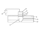
図1は、本発明の圧電体素子の一実施形態の構成を示す断面図である。
同図において、1は基板である。
基板1としては、シリコン(Si)やタングステン(W)などからなる半導体基板が好ましく用いられるが、ジルコニアやアルミナ、シリカなどのセラミックスのものを用いても構わない。また、シリコン基板の上に前記セラミックスを積層して多層構成としたり、白金、パラジウムなどの金属層を積層して用いても良い。
【0022】
図1において2および4は、それぞれ下部電極、上部電極であり、本発明の一実施態様においては、5〜500nm程度の厚みを有するCSD法により製造されたBSROで、組成式BaxSr1-xRuO3で表わされ、Baの原子分率xが、0< x <0.3であり、結晶構造がペロブスカイト型構造を有するBSROから形成される。
本発明におけるBSROは、上述したように、CSD法により製造することができる。
即ち、溶剤にBSROを生成することのできる金属アルコキシドまたは金属水酸化物等の原料を溶解または分散させた後、水を加えて、または水を加えて加水分解させて調製したBSROの前駆体(分散質と記載することがある)を含有する塗工液を基板上に塗工し、乾燥し、その後の熱処理工程において焼成を行うことにより得ることができる。
【0023】
溶剤としては、メタノール、エタノール、n−ブタノール、n−プロパノール、イソプロパノール等のアルコール系溶剤、テトラヒドロフラン、1,4−ジオキサン等のエーテル系溶剤、メチルセロソルブ、エチルセロソルブ等のセロソルブ系溶剤、N,N−ジメチルホルムアミド、N,N−ジメチルアセトアミド、N−メチルピロリドン系などのアミド系溶剤、アセトニトリル等のニトリル系溶剤が挙げられる。これらの中で好ましくはアルコール系溶剤である。
本発明におけるCSD法において用いられる溶剤の量は、金属アルコキシドに対しては、通常10倍モルから200倍モルであり、好ましくは20倍モルから100倍モルである。溶剤の量を10倍モルから200倍モルとすると、ゲル化が起こり易くなる一方で加水分解時の発熱を容易にコントロールすることができるので好ましい。
【0024】
ルテニウム化合物としては、アセチルアセトンルテニウム、トリス(2,2,6,6−テトラメチル−3,5−ヘプタンジアセチル)アセトナトルテニウム、ルテニウムオキサイド水和物、水酸化ルテニウム等、ルテニウムメトキシド、ルテニウムエトキシド、などのアルコキシドおよびそのアルキル置換体などが挙げられる。
【0025】
またルテニウムの無機塩化合物、具体的にはハロゲン化物、硝酸塩、リン酸塩、硫酸塩などまた有機酸塩化合物として具体的にはギ酸塩、酢酸塩、プロピオン酸塩、シュウ酸塩、クエン酸塩、リンゴ酸塩などの各種カルボン酸塩、ヒドロキシカルボン酸塩、またアセチルアセトナート錯体などを溶剤と混合してアルコキシドをin situ合成して用いても良い。
【0026】
また、金属アルコキシドまたは金属塩の加水分解には、例えば金属アルコキシドまたは金属塩の0.05倍モル〜2倍モルの水を用いることができ、より好ましくは0.5倍モル〜1.5倍モルの水を用いることができる。加水分解には、酸触媒または塩基触媒を用いてもよく、好ましくは、塩酸などの鉱酸や酢酸などの有機酸を用いることができる。
【0027】
ストロンチウム、バリウムを含む化合物も、前記ルテニウムと同様な化合物を用いることができる。
【0028】
上記塗工液は、下部電極を形成する場合は基板上に、また、上部電極を形成する場合は後述する圧電体薄膜の上に塗工し乾燥させる。
塗工方法は、スピンコート、ディップコート、バーコート、スプレーコートなど公知の塗工方法を用いることができる。また多数回の塗工、乾燥を行ってもよい。乾燥後の1層あたりの膜厚は特に問わないが、0.01μm〜0.5μmが好ましい。上部電極と下部電極の種類、厚みは同一であってもまた異なっていても良い。
【0029】
図1において、3は圧電体薄膜である。本発明においては、例えば、Pb1-xLax(ZryTi1-y)1-xO3(式中、0≦x<1、0≦y≦1)で表されるPLZT等のPZT系薄膜であり、CSD法等により製造することができる。
即ち、Pb、La、Zr、Tiのアルコキシド又は水酸化物等の原料を溶剤に分散させた後、水を加え加水分解して、PLZTを生成することのできる前駆体を調製しこれを含有する塗工液を調製し、これを基板上に塗工し、乾燥し、その後の熱処理工程による焼成を行うことによりPLZTから形成された圧電体膜を得ることができる。
【0030】
上記塗工液の調製に用いられる溶剤としては、メタノール、エタノール、n−ブタノール、n−プロパノール、イソプロパノール等のアルコール系溶剤、テトラヒドロフラン、1,4−ジオキサン等のエーテル系溶剤、メチルセロソルブ、エチルセロソルブ等のセロソルブ系溶剤、N,N−ジメチルホルムアミド、N,N−ジメチルアセトアミド、N−メチルピロリドン系などのアミド系溶剤、アセトニトリル等のニトリル系溶剤が挙げられる。これらの中で好ましくはアルコール系溶剤である。
本発明におけるCSD法による圧電体薄膜の調製において用いられる溶剤の量は、金属アルコキシドに対しては、通常10倍モルから200倍モルであり、好ましくは20倍モルから100倍モルである。溶剤の量を10倍モルから200倍モルとすると、ゲル化が起こり易くなる一方で加水分解時の発熱を容易にコントロールすることができるので好ましい。
【0031】
またPb化合物としては、水酸化鉛、鉛2−エトキシエトキシド、鉛メトキシド、鉛エトキシド、鉛n-プロポキシド、鉛i-プロポキシド、鉛n-ブトキシド、鉛i-ブトキシド、鉛t-ブトキシドなどのアルコキシドおよびそのアルキル置換体などが挙げられる。
【0032】
また鉛の無機塩化合物、具体的には、塩化物、硝酸塩、リン酸塩、硫酸塩など、また有機塩化合物、具体的には、ギ酸塩、酢酸塩、プロピオン酸塩、シュウ酸塩、クエン酸塩、リンゴ酸塩などの各種カルボン酸塩、ヒドロキシカルボン酸塩、またアセチルアセトナート錯体などを用いることができる。これらの無機塩化合物を溶剤と混合して水と反応させアルコキシドをin situ合成して用いても良い。
La、Zr、Tiについても同様の化合物または無機塩を用いることができる。
これらのPb、La、Zr、Tiの化合物を前記溶剤に分散し、加水分解を行い、PLZTの前駆体を含有する塗工液を得ることができる。
【0033】
上記各金属の仕込み比は、成膜時の焼成過程においてPbの消失がおこるため、あらかじめ塗工液作製時にPbの量を増やしておくことが好ましい。具体的には、原料のPb化合物の仕込みモル比を5%〜30%の範囲で増やすのが好ましい。
【0034】
また、金属アルコキシドまたは金属塩の加水分解には、例えば金属アルコキシドまたは金属塩の0.05倍モル〜2倍モルの水が用いられ、より好ましくは0.5倍モル〜1.5倍モルの水が用いられる。加水分解を行う際には、酸触媒または塩基触媒を用いるようにしてもよく、好ましくは、塩酸などの鉱酸や酢酸などの有機酸が用いられる。
【0035】
上記塗工液を、下部電極の上に塗工し、乾燥させ、塗工膜を形成する。
塗工方法は、スピンコート、ディップコート、バーコート、スプレーコートなど公知の塗工方法を用いることができる。また多数回の塗工、乾燥を行ってもよい。乾燥後の1層あたりの膜厚は特に問わないが、0.01μm〜5μmが好ましい。また総膜厚としては1μm〜30μm程度が好ましい。
【0036】
本発明の圧電体素子の製造方法についてさらに詳細に説明する。
【0037】
前記基板の上に前記塗工液を塗布し、前記CSD法により電極を形成し、下部電極とする。
塗工方法は特に限定されることはなくディップコート、スピンコート、バーコート、などの方法を用いることができる。スピンコート法により塗工する場合、電極用の塗工液を基板上に滴下し、スピンコータにより塗工液の均一な被膜(塗工膜と表わすことがある)を形成する。スピンコーティングでは、一般に回転数100〜500rpm程度の低速回転と回転数3000〜 5000rpm程度の高速回転が用いられる。すなわち、塗工液を滴下した基板を100〜500rpm程度の低速回転で1〜10秒程度回転させることにより、塗工液を基板表面全体に行き渡らせる。次いで、3000〜 5000rpm程度の高速回転で10〜30秒程度回転させることにより厚さの均一な塗工膜を形成する。
【0038】
次に、塗工膜に含まれる溶剤を除去するために、 150〜 200℃程度の温度で塗工膜を乾燥させる。さらに、乾燥した塗工膜に含まれる有機成分を除去するために、 300〜 500℃程度の温度で加熱処理する。膜厚を厚くする場合には、スピンコートと有機物除去の加熱処理とを交互に繰り返し行う。この後、500〜 700℃程度の温度で1〜60分程度熱処理(焼成と表わすことがある)することにより結晶化させ、BSROからなる下部電極を得る。
【0039】
焼成は不活性ガス雰囲気、酸素含有雰囲気(空気中等)等、任意の雰囲気下で行えばよく、常圧下または減圧下で行うこともできる。また、焼成の際に、段階的な昇温を行うようにしてもよい。このような焼成により、有機成分がほぼ消失して、緻密な構造の電極が得られる。
【0040】
このようにして形成された電極の上部に圧電体薄膜用の塗工液を塗工し、乾燥し、焼成して圧電体薄膜を形成する。
塗工液のスピンコーティングの条件は下部電極2のコーティングと同様にするのが好ましい。次いで、塗工膜に含まれる溶剤成分を除去するために、 150〜 200℃程度の温度で乾燥させる。さらに、乾燥した塗工膜に含まれる有機成分を除去するために、 300〜 500℃程度の温度で加熱処理する。膜厚を厚くする場合には、スピンコートと有機物除去の加熱処理とを交互に繰り返し行う。この後、500〜 700℃程度の温度で1〜60分程度焼成することにより結晶化させて、圧電体薄膜3を得る。この際の結晶化は、RTA(Rapid Thermal Annealing:高速熱処理)を適用してもよいし、また通常の電気炉熱を用いて焼成処理を行ってもかまわない。
【0041】
このとき、電極層と圧電体薄膜の接触界面では電極層を形成するBSROと圧電体薄膜層、例えば、PLZT層の双方の結晶系が同一でありなおかつ、格子定数がほぼ同じであるためにPLZTのエピタキシャル成長を促進する。また、PLZT膜の残留応力を緩和することにより圧電特性を改善することができる。
【0042】
焼成は、不活性ガス雰囲気、酸素含有雰囲気(空気中等)等、PbO雰囲気など、任意の雰囲気下で行えばよく、常圧下または減圧下で行うこともできる。また、焼成の際に、段階的な昇温を行うようにしてもよい。このような焼成により、有機成分がほぼ消失して、緻密な構造の圧電体膜が得られる。
【0043】
上部電極は圧電体薄膜の上部に下部電極と同様にして形成することができる。即ち上部電極は前記圧電体薄膜の上に電極用の塗工液を塗工し、乾燥し、焼成して形成する。
【0044】
このように本製造方法により圧電体薄膜と電極とを界面エピタキシャル成長させることにより圧電体薄膜と下部電極または上部電極との界面整合性を高め、良好な圧電特性を保持した圧電体素子を得ることができる。
【0045】
図2は、本発明の圧電体素子を用いたインクジェット式プリンターヘッド用のアクチュエータの概略を示す模式的断面図であり、本発明のインクジェット式記録ヘッドの一実施形態である、圧電体素子がアクチュエータに用いられたインクジェット式プリンターヘッドの一部を拡大して模式的に示した図である。図2に示したプリンターヘッドの基本構成は、従来と同様であり、ヘッド基台5と振動板7および圧電体素子とから構成されている。
【0046】
ヘッド基台5には、インクを噴射する多数のインクノズル(図示せず)、それぞれのインクノズルに個別に連通する多数のインク経路(図示せず)、および、それぞれのインク経路に個別に連通する多数のインク室6が形成されており、ヘッド基台5の上面全体を覆うように振動板7が取り付けられ、この振動板7によってヘッド基台5の全てのインク室6の上面開口が閉塞されている。振動板7上には、それぞれのインク室6と個別に対応した位置に、振動板7に振動駆動力を与えるための圧電体素子8が被着形成されている。
【0047】
そして、多数の圧電体素子8を電源9を制御して、所望の選択された圧電体素子8に電圧を印加することにより、圧電体素子8を変位させて、その部分の振動板7を振動させる。これにより、振動板7の振動に対応した部分のインク室6の容積が変化して、インク経路を通ってインクノズルからインクが押し出されて印刷が行われることになる。
【0048】
次に、本発明の薄膜キャパシタの実施形態を、ペロブスカイト型結晶構造を有するBSROによって構成されている下部電極および上部電極に挟持された誘電体を含むことを特徴とする薄膜キャパシタを例として取り上げ説明する。
【0049】
本発明においては、CSD法によって電極を形成した薄膜キャパシタの製造方法について詳細を説明するが、MOCVD法、スパッタリング法、蒸着法を電極の形成に適用することによっても、同様に、優れた性能を有する薄膜キャパシタを提供することが出来る。
【0050】
図8は本発明の薄膜キャパシタの一実施形態の製造工程の要部を示す説明図である。
同図において、基板12は、熱酸化SiO2膜を形成したSi基板などの半導体基板、MgO単結晶基板、SrTiO3単結晶基板などの基板である。
【0051】
まず、図8(a)に示すように、基板12の上側にBSRO導電性ペロブスカイト型結晶構造を有するBSROからなる下部電極13を成膜する。
下部電極13の成膜は、液相を用いた成膜プロセスにより実施することができる。液相を用いた成膜プロセスは、特に限定されるものではないが、CSD法、MOD(Metalorganic Deposition;メタルオーガニック・デポジション)法、水熱合成法などが適用される。CSD法やMOD法は、スピンコーティング、ディップコーティング、スプレーコーティング(噴霧コーティング)などのコーティング方法と組み合わせて利用することができる。
【0052】
CSD法とMOD法はよく似たプロセスであるが、これらは、反応過程に違いがあり、CSD法では加水分解縮重合反応が、MOD法では熱分解反応が用いられる。CSD法の場合には、まず、BSROの前駆体を含有する塗工液を基板12上に塗布し、塗工膜を乾燥し、乾燥した塗工膜を熱処理して縮重合反応させ、脱水反応および脱アルコール反応によりM−O−Mの架橋構造を形成させる。
MOD法の場合には、有機金属化合物を有機溶剤に溶解または分散させて調製した塗工液を、その状態(混合状態)で基板12上に塗布し、乾燥し、加熱して有機成分を分解・燃焼させ、M−O−Mの架橋構造を形成させる。
【0053】
BSROからなる下部電極13の成膜に、CSD法とスピンコーティングの組み合わせを適用する場合、まず、BSROの前駆体を含有する塗工液を調製する。塗工液としては、例えば、Baを含有するSrRuO3膜を形成する場合は、Br、SrとRuのアルコキシドを溶剤、例えば、2-メトキシエタノールに溶解または分散して調製したものを用いることができる。
【0054】
上記したような塗工液を基板12上に滴下し、スピンコータにより塗布し、均一な塗工膜を形成する。スピンコーティングでは、一般に回転数100〜500rpm程度の低速回転と回転数3000〜 5000rpm程度の高速回転が用いられる。すなわち、塗工液を滴下した基板を100〜500rpm程度の低速回転で1〜10秒程度回転させることにより、塗工液を基板表面全体に行き渡らせる。次いで、3000〜 5000rpm程度の高速回転で10〜30秒程度回転させることにより厚さの均一な塗工膜とする。
【0055】
次に、塗工膜に含まれる溶剤を除去するために、 150〜 200℃程度の温度で乾燥させる。さらに、塗工膜に含まれる有機成分を除去するために、 300〜 500℃程度の温度で加熱処理する。膜厚を厚くする場合には、スピンコートと有機物除去の加熱処理とを交互に繰り返し行う。この後、例えば酸素中にて500〜 700℃程度の温度で1〜60分程度熱処理することにより結晶化させ、BSRO膜からなる下部電極13を得る。
【0056】
CSD法を適用した場合、BSRO膜の結晶化は、後述する誘電体薄膜14の結晶化と同時に行ってもよいが、誘電体薄膜として例えばPZT系のものをスピンオンする場合には、BSRO膜を予め結晶化しておくことが好ましい。
【0057】
なお、上記した成膜工程はCSD法をスピンコーティングと組み合わせた場合について説明したが、各塗工液のコーティングには前述したように、ディップコーティング、スプレーコーティングなどを適用することもできる。
【0058】
上述したように、液相を用いた成膜法でBSRO膜を下部電極13として成膜することによって、液相内での分子レベルのオーダでの均一な混合状態に基づいて、組成ずれを生じさせることなく、膜組成の均一性に優れた下部電極13が得られる。電極のBSROと誘電体薄膜のPZT系酸化物双方の結晶系が同一であり、なおかつ、格子定数がほぼ同じであるために誘電体薄膜のPZT系酸化物のエピタキシャル成長を促進する。また、PZT系膜の残留応力を制御することができる。結果的に誘電体膜の電気特性の低下、例えば残留分極の減少、リーク電流の増大、疲労特性の劣化、誘電率の減少などを抑制することが可能となる。
【0059】
ここで、BSROからなる下部電極13の膜厚は通常の誘電体メモリと同様に5〜 500nm程度とすることができる。
【0060】
また、BSRO膜の加工の難しさから、これらの膜を薄くする場合には、BSRO膜のシート抵抗が高くなる傾向があるところから、下部電極13の膜厚を薄くする場合には、BSRO膜の下地として、Pt、Ru、Ir、Rh、RuO2 、IrO2などからなる導電層を形成するのが好ましい。
【0061】
次に、図8(b)に示すように、BSROからなる下部電極13上に誘電体薄膜14を成膜する。誘電体薄膜14には強誘電性または高誘電性を示す酸化物、例えば組成式ABO3(AおよびBは、それぞれ金属元素を表わす)で表されるペロブスカイト型結晶構造を有する酸化物(ペロブスカイト型酸化物と表わすことがある)が好ましく用いられる。誘電体薄膜14として用いるペロブスカイト型酸化物は、薄膜キャパシタの使用目的に応じて、誘電体としての機能を有する種々のぺロブスカイト型酸化物の中から選択して用いることができる。
【0062】
例えば、FRAMに適用する場合には、例えばPb(Zr,Ti)O3 (PZT)や(Pb,La)(Zr,Ti)O3 (PLZT)などのPb−Zr−Ti−O系酸化物、あるいはSrBi2 Ta2 O9などのSr−Bi−Ta−O系酸化物、Bi4 Ti3 O12などのBi−Ti−O系酸化物、Bi−Sr−Ti−O系酸化物などの強誘電性ペロブスカイト型酸化物が用いられる。
【0063】
また、BaリッチなBa1-x Srx TiO3やBaTiO3などのペロブスカイト型酸化物を用い、下部電極13との格子ミスマッチに起因する歪誘起強誘電性を利用して、FRAMの電荷蓄積部を構成することもできる。
【0064】
一方、DRAMとする場合には、Ba1-x Srx TiO3 (BSTOと略記することがある)、SrTiO3 (STOと略記することがある)、CaTiO3 、PbTiO3 、BaZrO3 、BaSnO3 、PbZrO3などの高誘電性ペロブスカイト型酸化物が用いられる。
【0065】
なお、上記したようなペロブスカイト型酸化物に、Ca、Sr、La、Nb、Mnなどを添加したものも用いることができる。
また、誘電体薄膜14の膜厚は特に限定されるものではないが、通常の誘電体メモリと同様に、10〜 300nm程度とすることができる。
【0066】
上述したようなペロブスカイト型酸化物からなる誘電体薄膜14についても、下部電極13と同様に、CSD法、MOD法などの成膜プロセスを適用して成膜することができる。CSD法やMOD法は前述したように、スピンコーティング、ディップコーティング、スプレーコーティングなどのコーティング方法と組み合わせて利用することができる。
【0067】
CSD法とスピンコーティングとを組み合わせて誘電体薄膜14を成膜する場合には、まず、誘電体薄膜の形成に必要な前駆体を含有する塗工液を調製する。代表的な強誘電体であるPZT系強誘電体では、例えば、Pbの出発原料として、例えば、酢酸鉛3水和物、Zrの出発原料として、例えば、ジルコニウムテトラプロポキシド、Tiの出発原料として、例えば、チタンテトライソプロポキシドを用い、これらを溶剤としての、例えば、2-メトキシエタノールに所定の比率で溶解または分散させて塗工液を調製する。
【0068】
上記したような塗工液を基板12上に形成した下部電極13の上に滴下し、スピンコータにより塗工液の均一な塗膜を形成する。スピンコーティングの条件は、下部電極13の成膜と同様とすることが好ましい。次いで、塗工膜に含まれる溶剤を除去するために、 150〜 200℃程度の温度で乾燥させる。さらに、乾燥した塗工膜に含まれる有機成分を除去するために、 300〜 500℃程度の温度で加熱処理する。膜厚を厚くする場合には、スピンコートと有機物除去の加熱処理とを交互に繰り返し行う。この後、酸素中にて500〜 700℃程度の温度で1〜60分程度熱処理することにより結晶化させて、誘電体薄膜14を得る。この際の結晶化は、RTA(高速熱処理)を適用してもよいし、また通常の電気炉熱処理でもかまわない。
【0069】
上述したように、液相を用いた成膜法でペロブスカイト型酸化物からなる誘電体薄膜14を成膜することによって、本発明では、下部電極を形成するBSROと誘電体薄膜を形成する、例えば、PZT系酸化物双方の結晶系が同一でありなおかつ、格子定数がほぼ同じであるためにPZT系酸化物のエピタキシャル成長を促進する。また、液相内での分子レベルのオーダでの均一な混合状態に基づいて、組成ずれを生じさせることなく、特性の均一な誘電体薄膜14が得られる。
【0070】
次に、図8(c)に示すように、誘電体薄膜14上に上部電極15を成膜することによって、薄膜キャパシタが作製される。なお、上部電極15にはPEP(Photo Etching Process ;フォトエッチングプロセス)などにより電極パターンを形成することができる。
【0071】
上部電極15は、下部電極13と同様にBSROで構成してもよいし、またPt、Ru、Ir、Rh、RuO2 、IrO2などを使用することも可能である。特に、上部電極15についても下部電極13と同様に、CSD法を用いて成膜することが好ましい。上部電極15をCSD法を用いて成膜することによって、上部電極を構成するBSROと、誘電体膜を構成する、例えば、PZT系酸化物双方の結晶系が同一でありなおかつ、格子定数がほぼ同じであるためにBSROのエピタキシャル成長を促進する。そのため良好な結晶性を示し、下部電極13と同様に電気特性に優れるBSRO電極が得られるため、基板12上に形成した微小なキャパシタセルの電気的特性の均一性をさらに高めることができる。
【0072】
上部電極15を液相を用いて成膜する場合の条件は、前述した下部電極13の成膜条件と同様とすることができる。
【0073】
本発明の薄膜キャパシタの製造方法においては、前述したように電極層と誘電体薄膜の接触界面では電極層を構成するBSROと誘電体薄膜を構成する、例えば、PZT系酸化物双方の結晶系が同一でありなおかつ、格子定数がほぼ同じであるためにPZT系酸化物のエピタキシャル成長を促進する。また、Si基板上において薄膜化した強誘電体の特性劣化については、特に応力の影響が大きいとされているが、本発明においては、PZT系膜等の誘電体薄膜の応力を制御することにより強誘電特性を改善することができる。
【0074】
本発明において、BSRO電極を用いることによる、PZT系酸化物のエピタキシャル成長の促進および応力の制御により、残留分極、リーク電流、疲労特性、誘電率などの、薄膜キャパシタの電気的特性を高めることができる。
【0075】
上述した実施形態では誘電体メモリの電荷蓄積部(薄膜キャパシタ)についてのみ説明したが、上述した実施形態による薄膜キャパシタはトランジスタと共にDRAMやFRAMなどの誘電体メモリを構成することもできる。本発明の薄膜キャパシタを用いることにより、DRAMやFRAMなどの誘電体メモリの信頼性や特性などを向上させることが可能となると共に、誘電体メモリの製造歩留りを高めることができる。
【0076】
【実施例】
以下に本発明に係わるBSRO膜製造の実施例及び比較例を挙げて本発明をより具体的に説明するが、本発明はこれらによって限定されるものではない。
【0077】
電極形成用の塗工液として以下の組成のものを作製した。
(Ba含有SRO塗工液の作製)
Ba:0.1、Sr:0.9、Ru:1の原子分率に相当する組成となるよう金属Sr、金属Ba、塩化ルテニウム(水和物)を2-メトキシエタノールに分散し加熱溶解し、Ba:0.1、Sr:0.9、Ru:1に相当する組成(原子分率)を有する前駆体を5%(酸化物換算濃度)含有するコート用の前駆体溶液(A液)を調製した。
Ba:0.2、Sr:0.8、Ru:1の原子分率に相当する組成となるよう金属Sr 、金属Ba 、塩化ルテニウム(水和物)を2-メトキシエタノールに分散し加熱溶解し、Ba:0.2、Sr:0.8、Ru:1に相当する組成(原子分率)を有する前駆体を5%(酸化物換算濃度)含有するコート用の前駆体溶液(B液)を調製した。
Ba:0.5、Sr:0.5、Ru:1の原子分率に相当する組成となるよう金属Sr、金属Ba、塩化ルテニウム(水和物)を2-メトキシエタノールに分散し加熱溶解し、Ba:0.5、Sr:0.5、Ru:1に相当する組成(原子分率)を有する前駆体を5%(酸化物換算濃度)含有するコート用の前駆体溶液(C液)を調製した。
【0078】
(SRO塗工液の作製)
Sr:1、Ru:1の原子分率に相当する組成となるよう金属Sr、塩化ルテニウム(水和物)を2-メトキシエタノールに分散し加熱溶解し、Sr:1、Ru:1に相当する組成(原子分率)を有する前駆体を5%(酸化物換算濃度)含有するコート用の前駆体溶液(D液)を調製した。
【0079】
圧電体薄膜形成用の塗工液として以下の組成のものを作製した。
(Pb:1.1、La:0.01、Zr:0.52、Ti:0.48の原子分率を有するPLZTに該当する組成を有する前駆体を含有する塗工液の作製)
Pb:1.1、La:0.01、Zr:0.52、Ti:0.48の原子分率に相当する組成となるよう酢酸鉛、ランタンイソプロポキシド、ジルコニウムブトキシド、チタンイソプロポキシドをメトキシエタノール中に分散し加熱溶解した。希塩酸を添加し加水分解しPb:1.1、La:0.01、Zr:0.52、Ti:0.48に相当する組成(原子分率)を有する前駆体を10%(酸化物換算濃度)含有する塗工液(E液)を得た。
また下記の市販のPZT塗工液を用いた。
三菱マテリアル(株)製PZT薄膜形成剤(10wt%PZT(110/52/48)(A6);商品名)をF液とした。
【0080】
圧電体素子およびその製造方法の実施例および比較例を示す。
【0081】
(実施例1)
図3および図4に示すような裏面の一部がくり抜かれたシリコン基板の表面に上記B液をスピンコーターにより塗工し、RTA(高速熱処理)法により600℃、10min焼成した。さらにB液をスピンコーターにより塗工し、RTA(高速熱処理)法により600℃、10min焼成し下部電極を形成した。得られた薄膜についてXRD測定を行ったところ、薄膜はペロブスカイト型結晶構造であり、(200)配向を示していた。更に、格子定数をペロブスカイト型結晶構造が擬似立方晶であるとして計算すると、3.970Åであった。下部電極の組成はBa:0.2、Sr:0.8、Ru:1.0(x=0.2)であった。
その上にF液を同様にスピンコーターで塗工した。RTAにより600℃、10min焼成した。さらにF液を用いて塗工、乾燥、焼成を10回繰り返し圧電体薄膜を形成した。
その上にB液を塗工しRTAにより600℃、10min焼成し上部電極を形成し、圧電体素子を得た(図5)。圧電体薄膜の中間部の組成を分析したところPb:1.0、Zr:0.52、Ti:0.48であった。
【0082】
(実施例2)
実施例1と同様の基板に、RFマグネトロンスパッタ法により基板温度600℃においてBSRO膜を製膜し下部電極を形成した。得られた薄膜についてXRD測定を行ったところ、薄膜はペロブスカイト型結晶構造であり、(200)配向を示していた。更に、格子定数をペロブスカイト型結晶構造が擬似立方晶であるとして計算すると、3.933Åであった。下部電極の組成はBa:0.1、Sr:0.9、Ru:1.0(x=0.1)であった。
その上にE液を同様にスピンコーターで塗工した。RTAにより600℃、10min焼成した。さらにE液を用いて塗工、乾燥、焼成を10回繰り返し圧電体薄膜を形成した。
その上に上記と同じ条件でBSRO膜を製膜し上部電極を形成して、圧電体素子を得た(図5)。圧電体薄膜の中間部の組成を分析したところPb:1.1、La:0.01、Zr:0.52、Ti:0.48であった。
【0083】
(比較例1)
実施例1と同様の基板に上記C液をスピンコーターにより塗工し、RTA(高速熱処理)法により600℃、10min焼成し下部電極を形成した。得られた薄膜についてXRD測定を行ったところ、薄膜はペロブスカイト型結晶構造であり、(200)配向を示していた。更に、格子定数をペロブスカイト型結晶構造が擬似立方晶であるとして計算すると、4.000Åであった。XRDではBaRuO3のピークも現れていることから固溶限界を超えていることがわかった。また、下部電極の組成はBa:0.5、Sr:0.5、Ru:1.0(x=0.5)であった。
その上にE液を同様にスピンコーターで塗工した。RTAにより600℃、10min焼成した。さらにE液を用いて塗工、乾燥、焼成を10回繰り返し圧電体薄膜を形成した。
その上にC液を塗工しRTAにより600℃、10min焼成し上部電極を形成して、圧電体素子を得た(図5)。圧電体薄膜の中間部の組成を分析したところPb:1.1、La:0.01、Zr:0.52、Ti:0.48であった。
【0084】
(比較例2)
実施例1と同様の基板に上記D液をスピンコーターにより塗工し、RTA(高速熱処理)法により600℃、10min焼成し下部電極を形成した。得られた薄膜についてXRD測定を行ったところ、薄膜はペロブスカイト型結晶構造であり、(200)配向を示していた。更に、格子定数をペロブスカイト型結晶構造が擬似立方晶であるとして計算すると、3.830Åであった。下部電極の組成はSr:1.0、Ru:1.0であった。
その上にF液を同様にスピンコーターで塗工した。RTAにより600℃、10min焼成した。さらにF液を用いて塗工、乾燥、焼成を10回繰り返し圧電体薄膜を形成した。
その上にD液を塗工しRTAにより600℃、10min焼成し上部電極を形成して、圧電体素子を得た(図5)。圧電体薄膜の中間部の組成を分析したところPb:1.0、Zr:0.52、Ti:0.48であった。
【0085】
(比較例3)
実施例1と同様の基板にPtをスパッタし下部電極を形成した。
その上にE液を同様にスピンコーターで塗工した。RTAにより600℃、10min焼成した。さらにE液を用いて塗工、乾燥、焼成を10回繰り返し圧電体薄膜を形成した。
その上にPtをスパッタし上部電極を形成して、圧電体素子を得た(図5)。圧電体薄膜の中間部の組成を分析したところPb:1.1、La:0.01、Zr:0.52、Ti:0.48であった。
【0086】
(評価)
実施例1〜2および比較例1〜3の圧電体素子を以下のように評価した。
上部電極と下部電極との間に10kHz、10Vの交流を印加しながら変位量をレーザードップラー法により測定し圧電体としての特性を評価した。
結果を表1に示す。表1に示した結果からわかるように実施例の圧電体は比較例の圧電体にくらべ、720時間の耐久試験後も変位量が大きく良好に動作している。
【0087】
【表1】

(インクジェット式記録ヘッドの作製)
(実施例3)
実施例1で作製した素子に、図6および図7で示すようなノズルを取り付けさらにインクを導入するための導入管を設けインクジェット式記録ヘッドとした。
【0089】
(比較例4)
比較例3で作製した素子に、図6および7で示すようなノズルを取り付けさらにインクを導入するための導入管を設けインクジェット式記録ヘッドとした。
【0090】
(評価)
実施例3および比較例4で作製したインクジェット式記録ヘッドに導入管よりインクジェット用インクを導入しインク室を満たした。次に上部電極と下部電極間に1〜20kHz、10Vの交流電圧を印加しインクの吐出の様子を顕微鏡で観察した。
その結果、実施例3のインクジェット式記録ヘッドは各周波数に追随しインク滴を吐出できた。一方、比較例4のインクジェット式記録ヘッドは15kHz〜20kHzの間でインク滴を均一性よく吐出することができなかった。
【0091】
薄膜キャパシタおよびその製造方法の実施例および比較例を示す。
【0092】
(実施例4)
表面に厚さ1μmの熱酸化SiO2膜を形成したシリコン基板の表面に上記A液をスピンコーターにより塗工し、RTA(高速熱処理)法により600℃、10min焼成し下部電極を形成した。得られた薄膜についてXRD測定を行ったところ、薄膜はペロブスカイト型結晶構造であり、(200)配向を示していた。更に、格子定数をペロブスカイト型結晶構造が擬似立方晶であるとして計算すると、3.933Åであった。下部電極の組成はBa:0.1、Sr:0.9、Ru:1.0(x=0.1)であった。
その上にF液を同様にスピンコーターで塗工した。RTAにより600℃、10min焼成した。さらにF液を用い塗工、乾燥、焼成を2回繰り返し誘電体薄膜を形成した。
その上にA液を塗工しRTAにより600℃、10min焼成し上部電極を形成した。誘電体薄膜の中間部の組成を分析したところPb:1.0、Zr:0.52、Ti:0.48であった。
【0093】
上記した上部電極(BSRO膜)上に、CVD(Chemical Vapor Deposition;化学気相成長)法により厚さ500μmのSiO2膜を形成した後、フォトレジストを用いてPEPで上部電極パターンを形成した。RIE(Reactive Ion Etching ;反応性イオンエッチング)で余分なBSRO膜を除去した後、レジストをアッシングにより除去して上部電極に電極パターンを付与し、薄膜キャパシタを得た。
【0094】
(実施例5)
実施例4と同様の基板に上記B液をスピンコーターにより塗工し、RTA(高速熱処理)法により600℃、10min焼成した。さらにB液をスピンコーターにより塗工し、RTA(高速熱処理)法により600℃、10min焼成し下部電極を形成した。得られた薄膜についてXRD測定を行ったところ、薄膜はペロブスカイト型結晶構造であり、(200)配向を示していた。更に、格子定数をペロブスカイト型結晶構造が擬似立方晶であるとして計算すると、3.970Åであった。下部電極の組成はBa:0.2、Sr:0.8、Ru:1.0(x=0.2)であった。
その上にF液を同様にスピンコーターで塗工した。RTAにより600℃、10min焼成した。さらにF液を用いて塗工、乾燥、焼成を2回繰り返し誘電体薄膜を形成した。
その上にB液を塗工しRTAにより600℃、10min焼成し、上部電極を形成した。誘電体薄膜の中間部の組成を分析したところPb:1.0、Zr:0.52、Ti:0.48であった。
さらに実施例4と同様にして電極パターンを付与し薄膜キャパシタを得た。
【0095】
(実施例6)
実施例4と同様の基板に、RFマグネトロンスパッタ法により基板温度600℃においてBSRO膜を製膜し下部電極を形成した。得られた薄膜についてXRD測定を行ったところ、薄膜はペロブスカイト型結晶構造であり、(200)配向を示していた。更に、格子定数をペロブスカイト型結晶構造が擬似立方晶であるとして計算すると、3.933Åであった。下部電極の組成はBa:0.1、Sr:0.9、Ru:1.0(x=0.1)であった。
その上にE液を同様にスピンコーターで塗工した。RTAにより600℃、10min焼成した。さらにE液を塗工、乾燥、焼成を2回繰り返し誘電体薄膜を形成した。
その上に上記と同じ条件でRFマグネトロンスパッタ法により上部電極を形成した。圧電体薄膜の中間部の組成を分析したところPb:1.1、La:0.01、Zr:0.52、Ti:0.48であった。
さらに実施例4と同様にして電極パターンを付与し、薄膜キャパシタを得た。
【0096】
(比較例5)
実施例4と同様の基板に上記C液をスピンコーターにより塗工し、RTA(高速熱処理)法により600℃、10min焼成し下部電極を形成した。得られた薄膜についてXRD測定を行ったところ、薄膜はペロブスカイト型結晶構造であり、(200)配向を示していた。更に、格子定数をペロブスカイト型結晶構造が立方晶であるとして計算すると、4.000Åであった。XRDではBaRuO3のピークが現れていることから固溶限界を超えていることがわかった。また、下部電極の組成はBa:0.5、Sr:0.5、Ru:1.0(x=0.5)であった。
その上にE液を同様にスピンコーターで塗工した。RTAにより600℃、10min焼成した。さらにE液を用いて塗工、乾燥、焼成を2回繰り返し誘電体薄膜を形成した。
その上にC液を塗工しRTAにより600℃、10min焼成し、上部電極を形成した。誘電体薄膜の中間部の組成を分析したところPb:1.1、La:0.01、Zr:0.52、Ti:0.48であった。
さらに実施例4と同様にして電極パターンを付与し薄膜キャパシタを得た。
【0097】
(比較例6)
実施例4と同様の基板に上記D液をスピンコーターにより塗工し、RTA(高速熱処理)法により600℃、10min焼成し下部電極を形成した。得られた薄膜についてXRD測定を行ったところ、薄膜はペロブスカイト型結晶構造であり、(200)配向を示していた。更に、格子定数をペロブスカイト型結晶構造が立方晶であるとして計算すると、3.830Åであった。下部電極の組成はSr:1.0、Ru:1.0であった。
その上にF液を同様にスピンコーターで塗工した。RTAにより600℃、10min焼成した。さらにF液を用いて塗工、乾燥、焼成を2回繰り返し誘電体薄膜を形成した。
その上にD液を塗工しRTAにより600℃、10min焼成し、上部電極を形成した。誘電体薄膜の中間部の組成を分析したところPb:1.0、Zr:0.52、Ti:0.48であった。
さらに実施例4と同様にして電極パターンを付与し薄膜キャパシタを得た。
【0098】
(比較例7)
実施例4と同様の基板にPtをスパッタし下部電極を形成した。
その上にE液をスピンコーターで塗工した。RTAにより600℃、10min焼成した。さらにE液を用いて塗工、乾燥、焼成を2回繰り返し誘電体薄膜を形成した。
その上にPtをスパッタし上部電極を形成した。誘電体薄膜の中間部の組成を分析したところPb:1.1、La:0.01、Zr:0.52、Ti:0.48であった。
さらに実施例4と同様にして電極パターンを付与し、薄膜キャパシタを得た。
【0099】
(評価)
実施例4〜6および比較例5〜7の薄膜キャパシタの電気特性として残留分極(Prと表わすことがある)、疲労特性を、測定電圧5Vで測定、評価した。
疲労特性は電圧±5Vを印可し、分極反転を1010回サイクル行ったときの残留分極2Prの値と2Pr初期値との差を求め評価した。30点で測定した値の平均値を表2に示す。表2に示した結果から明らかなように、比較例の薄膜キャパシタにくらべ、実施例の薄膜キャパシタは、耐疲労性(信頼性)に優れるものであることがわかる。
【0100】
【表2】
上記のように、本発明の製造方法によって製造したBSRO電極を有する圧電体素子は、圧電体薄膜と電極とを界面エピタキシャル成長させることにより圧電体薄膜と下部電極または上部電極との界面整合性を高め、良好な圧電特性を保持した圧電体素子であり、インクジェット式記録ヘッドの圧電体素子として優れた性能を有するだけでなく、他の装置にも広く用いることができる。
また、本発明のBSRO電極を有する薄膜キャパシタは、誘電体のエピタキシャル成長の促進および応力の制御により、残留分極、リーク電流、耐疲労特性、誘電率などの、薄膜キャパシタの電気的特性を高めることができ、これを用いたDRAMやFRAMなどの誘電体メモリの信頼性や特性などを向上させることが可能となると共に、誘電体メモリの製造歩留りを高くすることができる。
【0102】
【発明の効果】
以上説明したように、本発明のBSRO電極を用いることにより、優れた特性を示す圧電素子、薄膜キャパシタ、インクジェット式記録ヘッドを提供することが出来る。
【図面の簡単な説明】
【図1】本発明の圧電体素子の一実施形態の構成を示す断面図である。
【図2】本発明の圧電体素子を用いたインクジェット式プリンターヘッド用のアクチュエータの概略を示す模式的断面図である。
【図3】実施例1〜2、比較例1〜3で用いた基板の概略を示す斜視図である。
【図4】実施例1〜2、比較例1〜3で用いた基板の概略を示す断面図である。
【図5】実施例1〜2、比較例1〜3で作製した圧電体素子の概略を示す断面図である。
【図6】本発明のインクジェット式記録ヘッドのヘッド部の概略を示す模式的断面図である。
【図7】本発明のインクジェット式記録ヘッドのヘッド部の概略を示す斜視図である。
【図8】本発明の誘電体メモリの一実施形態の製造工程の要部を示す説明図である。
【符号の説明】
1 基板
2 下部電極
3 圧電体薄膜
4 上部電極
5 ヘッド基台
6 インク室
7 振動板
8 圧電体素子
9 電源
10 ノズル
11 インク導入管
12 基板
13 下部電極
14 誘電体薄膜
15 上部電極[0001]
BACKGROUND OF THE INVENTION
The present invention relates to a PZT-based memory or element such as PZT (lead zirconate titanate) or PLZT (lead lanthanum zirconate titanate) used as a ferroelectric memory material, piezoelectric element material, pyroelectric element material, etc. The present invention relates to a BSRO (barium-containing strontium ruthenate) electrode that is promising as a lower electrode layer, a method for manufacturing the electrode, a piezoelectric element including the electrode, an ink jet recording head including the piezoelectric element, and a thin film capacitor.
[0002]
[Prior art]
Conventionally, when using a PZT type ferroelectric film such as PZT or PLZT or a piezoelectric film as a member of a memory or piezoelectric element, platinum electrodes have been used for the upper and lower electrodes. In this case, the ferroelectric film and the piezoelectric film have excellent hysteresis in the squareness ratio with a large residual polarization and a small coercive electric field.12Polarization performance is not deteriorated even when repetitive pulses are applied more than once, and excellent fatigue resistance is required. However, when a platinum electrode is used, 109It is known that the polarization inversion charge is reduced by switching for about a cycle and the memory characteristics cannot be maintained.
[0003]
In recent years, LaNiO is a good conductor and has a perovskite crystal structure as well as PZT-based oxides.Three, SrRuOThree, YBa2CuThreeOxIt has been found that the use of oxide ceramics such as the lower electrode can greatly suppress fatigue due to the polarization reversal of the ferroelectric compared to the platinum electrode.
[0004]
The conductive oxide ceramics described above have the property of replenishing oxygen with respect to oxygen defects present in the vicinity of the electrode by reversing the polarization of the ferroelectric layer or piezoelectric layer, so that the accumulation of defects is suppressed. It is considered that polarization fatigue is suppressed. In addition, it has excellent diffusion barrier properties against Pb, etc., thus preventing oxygen deficiency in ferroelectric materials, piezoelectric materials, pyroelectric element materials, and fatigue of ferroelectric layers, piezoelectric layers, pyroelectric layers. Can be suppressed satisfactorily.
[Problems to be solved by the invention]
However, each of the ceramics has a lattice constant different from that of a PZT-based oxide such as PZT or PLZT. When these ceramics are stacked on a PZT-based thin film, the same crystal system is used. Although there is a possibility that the epitaxial growth is not sufficiently performed, and stress relaxation between the PZT-based layer and these ceramic layers is not sufficiently performed, it is difficult to maintain the piezoelectric characteristics, There is a problem that performance deteriorates.
[0005]
[Means for Solving the Problems]
In order to solve the above-mentioned problems, among the oxide ceramics listed above, SRO (strontium ruthenate (SrRuO) whose lattice constant is relatively close to that of PZT type.Three)) Was selected, and as a result of intensive studies, it was discovered that the addition of Ba, which is an atom having an ionic radius larger than Sr, which is a constituent element of SRO, found that the lattice constant was changed, thereby completing the present invention. Arrived.
[0006]
(1) The present inventionA piezoelectric element having a lower electrode, a PZT-based oxide piezoelectric film formed on the lower electrode, and an upper electrode provided on the piezoelectric body on a substrate,
The lower electrode is barium-containing strontium ruthenate having a perovskite crystal structure;Composition formulaButBaxSr1-xRuOThree(In the formula, 0 <x <0.3),The perovskite crystal structureButLattice constant obtained as pseudo cubic is3.933cm or more 3.970mmÅLess thanInAnd (200) oriented piezoelectric elementIt is about.
(2) The present invention further includes the Ba x Sr 1-x RuO Three In the composition formula, 0.05 <x <0.25, wherein the piezoelectric element according to (1) is provided.
(3) In the present invention, the piezoelectric body further has a perovskite crystal structure, and a composition formula Pb 1-x La x (Zr y Ti 1-y ) O Three (Wherein 0 ≦ x <1, 0 ≦ y ≦ 1). The present invention relates to the piezoelectric element according to (1) or (2) above.
[0007]
(4) In the piezoelectric element according to any one of (1) to (3), the crystal system of the lower electrode and the piezoelectric body of the PZT oxide is the same. It is about.
(5) The present invention further relates to the piezoelectric element according to any one of (1) to (4) above, wherein the PZT oxide piezoelectric material is epitaxially grown on the lower electrode. It is.
(6) The present invention further relates to the piezoelectric element according to any one of (1) to (5), wherein the thickness of the piezoelectric body of the PZT oxide is 1 μm or more and 30 μm or less. Is.
[0008]
(7The present invention further includesSaidelectrodeIs, CSD method, Formed by either MOCVD, sputtering or vapor deposition(1) characterized in thatOr (6)DescribedPiezoelectric elementIt is related with the manufacturing method.
(8) The present invention further relates to the method for manufacturing a piezoelectric element according to (7), wherein the piezoelectric body is formed by a CSD method.
[0009]
(9The present invention further includesSaidelectrodeIs formed by the CSD method, and includes a step of coating a substrate with a coating liquid containing a BSRO precursor, and the total thickness of the electrode after drying is 5 nm or more and 500 nm or less.Characterized by the above (7)Or (8)DescribedPiezoelectric elementIt is related with the manufacturing method.
(10) In the above (9), the present invention further includes the step of coating a plurality of times, and the film thickness per layer after drying is 0.01 μm or more and 0.5 μm or less. The present invention relates to a manufacturing method of the described piezoelectric element.
[0010]
(11The present invention further includesA nozzle for discharging liquid, a pressure chamber communicating with the nozzle, a diaphragm provided on one surface of the pressure chamber, and a volume provided in a position corresponding to the pressure chamber of the diaphragm. In an ink jet recording head provided with a piezoelectric element that exerts a change, the piezoelectric element includes:(1)Or (7)DescribedPiezoelectric elementIt is characterized byInkjet recording headIt is about.
(12) The present invention further includes a capacitor having a lower electrode, a PZT-based oxide dielectric formed on the lower electrode, and an upper electrode provided on the dielectric on a substrate,
The lower electrode is barium-containing strontium ruthenate having a perovskite crystal structure, and the composition formula is Ba x Sr 1-x RuO Three (Wherein 0 <x <0.3), the lattice constant determined as the perovskite crystal structure is a pseudo-cubic crystal is 3.933 to 3.970 and (200) -oriented. The present invention relates to a thin film capacitor.
[0011]
(13The present invention further includes the aboveBa x Sr 1-x RuO Three Composition formula ofIn0.05 <x <0.25It is characterized byThe thin film capacitor according to (12)It is about.
(14) In the present invention, further, the dielectric has a perovskite crystal structure, and a composition formula Pb 1-x La x (Zr y Ti 1-y ) O Three (Wherein 0 ≦ x <1, 0 ≦ y ≦ 1). The present invention relates to the thin film capacitor according to (12) above.
[0012]
(15The present invention further includesThe crystal system of the lower electrode and the dielectric of the PZT oxide is the sameIt is characterized byAny one of (12) to (14)The present invention relates to a thin film capacitor.
(16) The present invention further relates to the thin film capacitor according to any one of (12) to (15), wherein the PZT-based oxide dielectric is epitaxially grown on the lower electrode. is there.
[0013]
(17The present invention further includes the aboveThe substrate is SiO 2 The lower electrode is made of SiO. 2 Formed on the membraneIt is characterized byAny of (12) to (16)The present invention relates to a thin film capacitor.
(18) The present invention further relates to the thin film capacitor according to any one of (12) to (17), wherein the PZT oxide dielectric has a thickness of 10 nm to 300 nm. It is.
[0014]
(19The present invention further includesThe electrode is formed by any of CSD method, MOCVD method, sputtering method or vapor deposition method.It is characterized byThe method for manufacturing a thin film capacitor according to any one of (12) to (18)It is about.
(20) The present invention further relates to the method for manufacturing a thin film capacitor according to (19), wherein the dielectric is formed by a CSD method.
(21) The present invention further includes a step of applying a coating liquid containing a BSRO precursor to a substrate in the method for forming the electrode by the CSD method, and the total thickness of the electrode after drying is 5 nm. The present invention relates to the method for producing a thin film capacitor according to (19) or (20), wherein the thickness is 500 nm or less.
[0015]
DETAILED DESCRIPTION OF THE INVENTION
In the BSRO forming the electrode of the present invention, the added Ba replaces Sr at the position occupied by Sr in the SRO crystal, and the difference in the ionic radius between Sr and Ba causes distortion in the original SRO crystal lattice, resulting in a lattice constant. Changes.
The atomic fraction x of Ba of BSRO in the present invention is such that Ba is dissolved in SRO and BaRuOThreeThe range in which no crystal is formed is desirable, and the limit amount of substitution depends on the preparation method, but the atomic fraction x of Ba needs to be 0 <x <0.3, preferably 0.05 <x <0.25.
[0016]
The method for producing BSRO in the present invention is necessary if the produced BSRO is sufficiently crystallized and if the added Ba substitutes Sr for the site occupied by Sr in the BSRO crystal. Various methods can be taken depending on the balance with the form to be performed.
[0017]
For example, by mixing and calcining raw material powders (generally oxides and carbonates) and then calcining them, or by firing the raw materials into solutions or dispersing them in a solvent and applying them to a substrate and firing them. CSD method (Chemical Solution Deposition; sol-gel method), MOCVD method (Metal Organic Chemical Vapor Deposition), or sputtering method, vapor deposition method, etc. are used to obtain the target product. it can.
[0018]
The raw material for producing BSRO in the present invention is not particularly limited as long as necessary purity can be ensured, and various raw materials can be used depending on the production method.
In the solid phase reaction method, a metal oxide or carbonate constituting BSRO is used as a raw material.
In the CSD method, in order to make a precursor solution, any metal raw material that can be dissolved or dispersed in a solvent such as alcohol, such as a simple metal, chloride, nitrate, acetate, alkoxide or the like can be used. .
[0019]
Hereinafter, a mode for carrying out the present invention will be described first with respect to a piezoelectric element including a BSRO electrode and a lower electrode formed from the BSRO and a piezoelectric body sandwiched between the upper electrodes.
[0020]
In the present invention, the manufacturing method of a piezoelectric element that forms a BSRO electrode using the CSD method will be described as an example, and the details will be described. The formation method of the BSRO electrode is an MOCVD method, a sputtering method, or a vapor deposition method. Also by these methods, a promising BSRO film can be formed as a lower electrode layer or an upper electrode layer of a PZT-based (lead zirconate titanate) thin film as in the CSD method.
[0021]
FIG. 1 is a cross-sectional view showing a configuration of an embodiment of a piezoelectric element of the present invention.
In the figure, reference numeral 1 denotes a substrate.
As the substrate 1, a semiconductor substrate made of silicon (Si), tungsten (W), or the like is preferably used, but ceramics such as zirconia, alumina, or silica may be used. Further, the ceramics may be laminated on a silicon substrate to form a multilayer structure, or a metal layer such as platinum or palladium may be laminated.
[0022]
In FIG. 1, 2 and 4 are a lower electrode and an upper electrode, respectively. In one embodiment of the present invention, a BSRO manufactured by a CSD method having a thickness of about 5 to 500 nm has a composition formula BaxSr1-xRuOThreeThe atomic fraction x of Ba is 0 <x <0.3, and the crystal structure is formed of BSRO having a perovskite structure.
As described above, the BSRO in the present invention can be manufactured by the CSD method.
That is, a precursor of BSRO prepared by dissolving or dispersing a raw material such as a metal alkoxide or a metal hydroxide capable of generating BSRO in a solvent, and then adding water or hydrolyzing it with water ( It may be obtained by applying a coating liquid containing a dispersion (which may be described as a dispersoid) on a substrate, drying, and baking in a subsequent heat treatment step.
[0023]
Solvents include alcohol solvents such as methanol, ethanol, n-butanol, n-propanol and isopropanol, ether solvents such as tetrahydrofuran and 1,4-dioxane, cellosolve solvents such as methyl cellosolve and ethyl cellosolve, N, N Examples include amide solvents such as dimethylformamide, N, N-dimethylacetamide, and N-methylpyrrolidone, and nitrile solvents such as acetonitrile. Of these, alcohol solvents are preferred.
The amount of the solvent used in the CSD method in the present invention is usually 10 to 200 times mol, preferably 20 to 100 times mol for the metal alkoxide. When the amount of the solvent is 10 to 200 times mol, gelation is likely to occur, while heat generation during hydrolysis can be easily controlled, which is preferable.
[0024]
Examples of ruthenium compounds include acetylacetone ruthenium, tris (2,2,6,6-tetramethyl-3,5-heptanediacetyl) acetonatorenthene, ruthenium oxide hydrate, ruthenium hydroxide, ruthenium methoxide, ruthenium ethoxide. And alkoxides thereof, and alkyl-substituted products thereof.
[0025]
In addition, ruthenium inorganic salt compounds, specifically halides, nitrates, phosphates, sulfates, etc., and organic acid salt compounds specifically include formate, acetate, propionate, oxalate, citrate. Alternatively, various carboxylates such as malate, hydroxycarboxylate, acetylacetonate complex, etc. may be mixed with a solvent to synthesize alkoxide in situ.
[0026]
In addition, for the hydrolysis of the metal alkoxide or metal salt, for example, 0.05 to 2 times moles of water of the metal alkoxide or metal salt can be used, more preferably 0.5 to 1.5 times mole. Molar water can be used. For the hydrolysis, an acid catalyst or a base catalyst may be used. Preferably, a mineral acid such as hydrochloric acid or an organic acid such as acetic acid can be used.
[0027]
As the compound containing strontium and barium, the same compound as the ruthenium can be used.
[0028]
The coating solution is applied on a substrate when forming the lower electrode, and is applied onto a piezoelectric thin film described later when forming the upper electrode and dried.
As a coating method, a known coating method such as spin coating, dip coating, bar coating, spray coating, or the like can be used. Moreover, you may perform many times of coating and drying. The film thickness per layer after drying is not particularly limited, but is preferably 0.01 μm to 0.5 μm. The types and thicknesses of the upper electrode and the lower electrode may be the same or different.
[0029]
In FIG. 1, 3 is a piezoelectric thin film. In the present invention, for example, Pb1-xLax(ZryTi1-y)1-xOThreeA PZT-based thin film such as PLZT represented by (where 0 ≦ x <1, 0 ≦ y ≦ 1), and can be manufactured by a CSD method or the like.
That is, after a raw material such as Pb, La, Zr, Ti alkoxide or hydroxide is dispersed in a solvent, water is added and hydrolyzed to prepare a precursor capable of generating PLZT and contain it. A piezoelectric film formed from PLZT can be obtained by preparing a coating solution, coating the substrate on a substrate, drying the coating solution, and performing firing in a subsequent heat treatment step.
[0030]
Solvents used for the preparation of the coating liquid include alcohol solvents such as methanol, ethanol, n-butanol, n-propanol and isopropanol, ether solvents such as tetrahydrofuran and 1,4-dioxane, methyl cellosolve and ethyl cellosolve. And the like, amide solvents such as N, N-dimethylformamide, N, N-dimethylacetamide and N-methylpyrrolidone, and nitrile solvents such as acetonitrile. Of these, alcohol solvents are preferred.
The amount of the solvent used in the preparation of the piezoelectric thin film by the CSD method in the present invention is usually 10 to 200 times mol, preferably 20 to 100 times mol for the metal alkoxide. When the amount of the solvent is 10 to 200 times mol, gelation is likely to occur, while heat generation during hydrolysis can be easily controlled, which is preferable.
[0031]
Pb compounds include lead hydroxide, lead 2-ethoxyethoxide, lead methoxide, lead ethoxide, lead n-propoxide, lead i-propoxide, lead n-butoxide, lead i-butoxide, lead t-butoxide, etc. Alkoxides and alkyl-substituted products thereof.
[0032]
In addition, inorganic lead compounds such as chlorides, nitrates, phosphates, sulfates, etc., and organic salt compounds such as formate, acetate, propionate, oxalate, citric acid, etc. Various carboxylates such as acid salts and malates, hydroxycarboxylates, and acetylacetonate complexes can be used. These inorganic salt compounds may be mixed with a solvent and reacted with water to synthesize an alkoxide in situ.
Similar compounds or inorganic salts can be used for La, Zr, and Ti.
These Pb, La, Zr, and Ti compounds are dispersed in the solvent and hydrolyzed to obtain a coating solution containing a PLZT precursor.
[0033]
As for the charging ratio of each of the above metals, it is preferable to increase the amount of Pb in advance during the preparation of the coating liquid because Pb disappears during the firing process during film formation. Specifically, it is preferable to increase the charged molar ratio of the raw material Pb compound in the range of 5% to 30%.
[0034]
In addition, for the hydrolysis of the metal alkoxide or metal salt, for example, 0.05 to 2 times moles of water of the metal alkoxide or metal salt is used, and more preferably 0.5 to 1.5 times moles of water. Water is used. When performing the hydrolysis, an acid catalyst or a base catalyst may be used. Preferably, a mineral acid such as hydrochloric acid or an organic acid such as acetic acid is used.
[0035]
The coating solution is applied onto the lower electrode and dried to form a coating film.
As a coating method, a known coating method such as spin coating, dip coating, bar coating, spray coating, or the like can be used. Moreover, you may perform many times of coating and drying. The film thickness per layer after drying is not particularly limited, but is preferably 0.01 μm to 5 μm. The total film thickness is preferably about 1 μm to 30 μm.
[0036]
The method for manufacturing a piezoelectric element of the present invention will be described in more detail.
[0037]
The coating solution is applied onto the substrate, and an electrode is formed by the CSD method to form a lower electrode.
The coating method is not particularly limited, and methods such as dip coating, spin coating, and bar coating can be used. When coating is performed by a spin coating method, a coating solution for an electrode is dropped on the substrate, and a uniform film (sometimes referred to as a coating film) of the coating solution is formed by a spin coater. In spin coating, generally, a low-speed rotation of about 100 to 500 rpm and a high-speed rotation of about 3000 to 5000 rpm are used. That is, the substrate onto which the coating liquid is dropped is rotated at a low speed of about 100 to 500 rpm for about 1 to 10 seconds to spread the coating liquid over the entire surface of the substrate. Next, a coating film having a uniform thickness is formed by rotating at a high speed of about 3000 to 5000 rpm for about 10 to 30 seconds.
[0038]
Next, in order to remove the solvent contained in the coating film, the coating film is dried at a temperature of about 150 to 200 ° C. Furthermore, in order to remove organic components contained in the dried coating film, heat treatment is performed at a temperature of about 300 to 500 ° C. In order to increase the film thickness, spin coating and organic substance removal heat treatment are alternately repeated. Thereafter, it is crystallized by heat treatment (sometimes referred to as firing) at a temperature of about 500 to 700 ° C. for about 1 to 60 minutes to obtain a lower electrode made of BSRO.
[0039]
Firing may be performed in an arbitrary atmosphere such as an inert gas atmosphere or an oxygen-containing atmosphere (in the air or the like), and may be performed under normal pressure or reduced pressure. Further, a stepwise temperature increase may be performed during firing. By such firing, the organic component is almost lost, and an electrode having a dense structure is obtained.
[0040]
A piezoelectric thin film is formed by applying a coating liquid for a piezoelectric thin film on the electrode thus formed, drying, and firing.
The conditions for spin coating of the coating liquid are preferably the same as those for coating the
[0041]
At this time, at the contact interface between the electrode layer and the piezoelectric thin film, the crystal system of both the BSRO forming the electrode layer and the piezoelectric thin film layer, for example, the PLZT layer, is the same, and the lattice constant is substantially the same. Promote the epitaxial growth of. Further, the piezoelectric characteristics can be improved by relaxing the residual stress of the PLZT film.
[0042]
Firing may be performed in an arbitrary atmosphere such as an inert gas atmosphere, an oxygen-containing atmosphere (in the air, etc.), a PbO atmosphere, or the like, and may be performed under normal pressure or reduced pressure. Further, a stepwise temperature increase may be performed during firing. By such firing, the organic component is almost eliminated, and a piezoelectric film having a dense structure can be obtained.
[0043]
The upper electrode can be formed on the piezoelectric thin film in the same manner as the lower electrode. That is, the upper electrode is formed by applying an electrode coating liquid on the piezoelectric thin film, drying, and firing.
[0044]
In this way, the piezoelectric thin film and the electrode can be epitaxially grown by this manufacturing method to enhance the interface matching between the piezoelectric thin film and the lower electrode or the upper electrode, thereby obtaining a piezoelectric element having good piezoelectric characteristics. it can.
[0045]
FIG. 2 is a schematic cross-sectional view showing an outline of an actuator for an ink jet printer head using the piezoelectric element of the present invention. The piezoelectric element according to an embodiment of the ink jet recording head of the present invention is an actuator. It is the figure which expanded and showed typically a part of ink-jet printer head used for. The basic configuration of the printer head shown in FIG. 2 is the same as that of the prior art, and includes a
[0046]
The
[0047]
A number of
[0048]
Next, an embodiment of the thin film capacitor of the present invention will be described by taking as an example a thin film capacitor including a lower electrode made of BSRO having a perovskite crystal structure and a dielectric sandwiched between the upper electrodes. To do.
[0049]
In the present invention, the details of a method for manufacturing a thin film capacitor in which electrodes are formed by the CSD method will be described. A thin film capacitor can be provided.
[0050]
FIG. 8 is an explanatory view showing the main part of the manufacturing process of one embodiment of the thin film capacitor of the present invention.
In the figure, the
[0051]
First, as shown in FIG. 8A, a
The
[0052]
Although the CSD method and the MOD method are very similar processes, there are differences in the reaction process. The CSD method uses a hydrolytic condensation polymerization reaction, and the MOD method uses a thermal decomposition reaction. In the case of the CSD method, first, a coating liquid containing a precursor of BSRO is applied onto the
In the case of the MOD method, a coating solution prepared by dissolving or dispersing an organometallic compound in an organic solvent is applied on the
[0053]
When a combination of the CSD method and spin coating is applied to the film formation of the
[0054]
The coating liquid as described above is dropped on the
[0055]
Next, in order to remove the solvent contained in the coating film, it is dried at a temperature of about 150 to 200 ° C. Furthermore, in order to remove organic components contained in the coating film, heat treatment is performed at a temperature of about 300 to 500 ° C. In order to increase the film thickness, spin coating and organic substance removal heat treatment are alternately repeated. Thereafter, crystallization is performed by, for example, heat treatment in oxygen at a temperature of about 500 to 700 ° C. for about 1 to 60 minutes to obtain the
[0056]
When the CSD method is applied, the crystallization of the BSRO film may be performed simultaneously with the crystallization of the dielectric
[0057]
In the film forming process described above, the case where the CSD method is combined with spin coating has been described. However, as described above, dip coating, spray coating, or the like can be applied to the coating of each coating solution.
[0058]
As described above, the BSRO film is formed as the
[0059]
Here, the film thickness of the
[0060]
Further, due to the difficulty in processing the BSRO film, when these films are thinned, the sheet resistance of the BSRO film tends to increase. As the base of Pt, Ru, Ir, Rh, RuO2 , IrO2It is preferable to form a conductive layer made of or the like.
[0061]
Next, as shown in FIG. 8B, a dielectric
[0062]
For example, when applied to FRAM, for example, Pb (Zr, Ti) OThree (PZT) or (Pb, La) (Zr, Ti) OThree Pb—Zr—Ti—O-based oxides such as (PLZT) or SrBi2 Ta2 O9Sr—Bi—Ta—O-based oxides such as BiFour TiThree O12Ferroelectric perovskite oxides such as Bi—Ti—O-based oxides and Bi—Sr—Ti—O-based oxides are used.
[0063]
Ba-rich Ba1-x Srx TiOThreeAnd BaTiOThreeThe charge storage portion of the FRAM can also be configured by using a perovskite type oxide such as that and utilizing strain-induced ferroelectricity caused by lattice mismatch with the
[0064]
On the other hand, in the case of DRAM, Ba1-x Srx TiOThree (May be abbreviated as BSTO), SrTiOThree (May be abbreviated as STO), CaTiOThree , PbTiOThree , BaZrOThree , BaSnOThree , PbZrOThreeHigh dielectric perovskite oxides such as are used.
[0065]
Note that a perovskite oxide having Ca, Sr, La, Nb, Mn, or the like added thereto can be used.
The thickness of the dielectric
[0066]
The dielectric
[0067]
When the dielectric
[0068]
The coating liquid as described above is dropped on the
[0069]
As described above, by forming the dielectric
[0070]
Next, as shown in FIG. 8C, the upper electrode 15 is formed on the dielectric
[0071]
The upper electrode 15 may be composed of BSRO like the
[0072]
The conditions for forming the upper electrode 15 using the liquid phase can be the same as those for forming the
[0073]
In the method for manufacturing a thin film capacitor according to the present invention, as described above, at the contact interface between the electrode layer and the dielectric thin film, the BSRO constituting the electrode layer and the dielectric thin film are formed. Since they are the same and have substantially the same lattice constant, the epitaxial growth of the PZT-based oxide is promoted. In addition, it is said that the influence of stress is particularly great on the characteristic deterioration of the ferroelectric thinned on the Si substrate, but in the present invention, by controlling the stress of the dielectric thin film such as a PZT film. Ferroelectric properties can be improved.
[0074]
In the present invention, the electrical characteristics of a thin film capacitor such as remanent polarization, leakage current, fatigue characteristics, and dielectric constant can be enhanced by promoting the epitaxial growth of PZT-based oxide and controlling the stress by using a BSRO electrode. .
[0075]
In the above-described embodiment, only the charge storage portion (thin film capacitor) of the dielectric memory has been described. However, the thin film capacitor according to the above-described embodiment can constitute a dielectric memory such as a DRAM or FRAM together with a transistor. By using the thin film capacitor of the present invention, it is possible to improve the reliability and characteristics of a dielectric memory such as a DRAM or FRAM, and to increase the production yield of the dielectric memory.
[0076]
【Example】
The present invention will be described more specifically below with reference to examples and comparative examples of BSRO membrane production according to the present invention, but the present invention is not limited thereto.
[0077]
The following composition was prepared as a coating liquid for electrode formation.
(Preparation of Ba-containing SRO coating solution)
Metal Sr, metal Ba, and ruthenium chloride (hydrate) are dispersed in 2-methoxyethanol and dissolved by heating so that the composition corresponds to the atomic fraction of Ba: 0.1, Sr: 0.9, and Ru: 1. Ba: 0.1 A coating precursor solution (solution A) containing 5% (oxide equivalent concentration) of a precursor having a composition (atomic fraction) corresponding to Sr: 0.9 and Ru: 1 was prepared.
Metal Sr, metal Ba, and ruthenium chloride (hydrate) are dispersed in 2-methoxyethanol so that the composition corresponds to the atomic fraction of Ba: 0.2, Sr: 0.8, and Ru: 1, Ba: 0.2 A precursor solution for coating (liquid B) containing 5% (oxide equivalent concentration) of a precursor having a composition (atomic fraction) corresponding to Sr: 0.8 and Ru: 1 was prepared.
Metal Sr, metal Ba, and ruthenium chloride (hydrate) are dispersed in 2-methoxyethanol and dissolved by heating so that the composition corresponds to the atomic fraction of Ba: 0.5, Sr: 0.5, Ru: 1, Ba: 0.5 A precursor solution for coating (C solution) containing 5% (oxide equivalent concentration) of a precursor having a composition (atomic fraction) corresponding to Sr: 0.5 and Ru: 1 was prepared.
[0078]
(Preparation of SRO coating solution)
Metal Sr and ruthenium chloride (hydrate) are dispersed in 2-methoxyethanol and dissolved by heating so that the composition corresponds to the atomic fraction of Sr: 1 and Ru: 1, and corresponds to Sr: 1 and Ru: 1. A coating precursor solution (solution D) containing 5% (oxide equivalent concentration) of a precursor having a composition (atomic fraction) was prepared.
[0079]
The following composition was prepared as a coating liquid for forming a piezoelectric thin film.
(Preparation of a coating solution containing a precursor having a composition corresponding to PLZT having an atomic fraction of Pb: 1.1, La: 0.01, Zr: 0.52, Ti: 0.48)
Pb: 1.1, La: 0.01, Zr: 0.52, Ti: 0.48 Lead acetate, lanthanum isopropoxide, zirconium butoxide, titanium isopropoxide are dispersed in methoxyethanol and dissolved by heating to a composition corresponding to the atomic fraction. did. A coating solution containing 10% (oxide equivalent concentration) of a precursor having a composition (atomic fraction) corresponding to Pb: 1.1, La: 0.01, Zr: 0.52, Ti: 0.48 by hydrolysis with dilute hydrochloric acid ( E liquid) was obtained.
The following commercially available PZT coating solution was used.
A PZT thin film forming agent (10 wt% PZT (110/52/48) (A6); trade name) manufactured by Mitsubishi Materials Corporation was used as liquid F.
[0080]
Examples and comparative examples of the piezoelectric element and the manufacturing method thereof are shown.
[0081]
(Example 1)
The above-mentioned B liquid was applied to the surface of the silicon substrate from which a part of the back surface was hollowed out as shown in FIGS. 3 and 4 by a spin coater and baked at 600 ° C. for 10 minutes by an RTA (rapid heat treatment) method. Further, the liquid B was applied by a spin coater and baked at 600 ° C. for 10 minutes by an RTA (rapid heat treatment) method to form a lower electrode. When the XRD measurement was performed on the obtained thin film, the thin film had a perovskite crystal structure and exhibited (200) orientation. Further, when the lattice constant was calculated on the assumption that the perovskite type crystal structure was pseudo cubic, it was 3.970Å. The composition of the lower electrode was Ba: 0.2, Sr: 0.8, Ru: 1.0 (x = 0.2).
On top of that, the F solution was similarly coated with a spin coater. Firing was performed at 600 ° C. for 10 minutes using RTA. Further, coating, drying and firing were repeated 10 times using the F solution to form a piezoelectric thin film.
Liquid B was coated on it and fired at 600 ° C. for 10 minutes by RTA to form an upper electrode, thereby obtaining a piezoelectric element (FIG. 5). The composition of the intermediate portion of the piezoelectric thin film was analyzed and found to be Pb: 1.0, Zr: 0.52, Ti: 0.48.
[0082]
(Example 2)
A BSRO film was formed on the same substrate as in Example 1 by a RF magnetron sputtering method at a substrate temperature of 600 ° C. to form a lower electrode. When the XRD measurement was performed on the obtained thin film, the thin film had a perovskite crystal structure and exhibited (200) orientation. Further, when the lattice constant was calculated on the assumption that the perovskite crystal structure was pseudo cubic, it was 3.933%. The composition of the lower electrode was Ba: 0.1, Sr: 0.9, Ru: 1.0 (x = 0.1).
On top of that, the E liquid was similarly coated with a spin coater. Firing was performed at 600 ° C. for 10 minutes using RTA. Furthermore, coating, drying and firing were repeated 10 times using the E solution to form a piezoelectric thin film.
A BSRO film was formed thereon under the same conditions as above to form an upper electrode, thereby obtaining a piezoelectric element (FIG. 5). Analysis of the composition of the intermediate portion of the piezoelectric thin film revealed Pb: 1.1, La: 0.01, Zr: 0.52, and Ti: 0.48.
[0083]
(Comparative Example 1)
The liquid C was applied to the same substrate as in Example 1 using a spin coater, and baked at 600 ° C. for 10 minutes by an RTA (rapid heat treatment) method to form a lower electrode. When the XRD measurement was performed on the obtained thin film, the thin film had a perovskite crystal structure and exhibited (200) orientation. Further, when the lattice constant was calculated on the assumption that the perovskite type crystal structure was pseudo cubic, it was 4.000Å. BaRuO in XRDThreeIt was found that the solid solution limit was exceeded because of the peak of. The composition of the lower electrode was Ba: 0.5, Sr: 0.5, Ru: 1.0 (x = 0.5).
On top of that, the E liquid was similarly coated with a spin coater. Firing was performed at 600 ° C. for 10 minutes using RTA. Furthermore, coating, drying and firing were repeated 10 times using the E solution to form a piezoelectric thin film.
The C liquid was applied thereon and baked at 600 ° C. for 10 minutes by RTA to form an upper electrode, thereby obtaining a piezoelectric element (FIG. 5). Analysis of the composition of the intermediate portion of the piezoelectric thin film revealed Pb: 1.1, La: 0.01, Zr: 0.52, and Ti: 0.48.
[0084]
(Comparative Example 2)
The above solution D was applied to the same substrate as in Example 1 using a spin coater, and baked at 600 ° C. for 10 minutes by an RTA (rapid heat treatment) method to form a lower electrode. When the XRD measurement was performed on the obtained thin film, the thin film had a perovskite crystal structure and exhibited (200) orientation. Further, when the lattice constant was calculated on the assumption that the perovskite type crystal structure was pseudo cubic, it was 3.830%. The composition of the lower electrode was Sr: 1.0 and Ru: 1.0.
On top of that, the F solution was similarly coated with a spin coater. Firing was performed at 600 ° C. for 10 minutes using RTA. Further, coating, drying and firing were repeated 10 times using the F solution to form a piezoelectric thin film.
The D liquid was coated thereon and baked at 600 ° C. for 10 minutes by RTA to form an upper electrode to obtain a piezoelectric element (FIG. 5). The composition of the intermediate portion of the piezoelectric thin film was analyzed and found to be Pb: 1.0, Zr: 0.52, Ti: 0.48.
[0085]
(Comparative Example 3)
A lower electrode was formed by sputtering Pt on the same substrate as in Example 1.
On top of that, the E liquid was similarly coated with a spin coater. Firing was performed at 600 ° C. for 10 minutes using RTA. Furthermore, coating, drying and firing were repeated 10 times using the E solution to form a piezoelectric thin film.
A Pt was sputtered thereon to form an upper electrode to obtain a piezoelectric element (FIG. 5). Analysis of the composition of the intermediate portion of the piezoelectric thin film revealed Pb: 1.1, La: 0.01, Zr: 0.52, and Ti: 0.48.
[0086]
(Evaluation)
The piezoelectric elements of Examples 1-2 and Comparative Examples 1-3 were evaluated as follows.
The displacement was measured by the laser Doppler method while applying 10kHz, 10V AC between the upper electrode and the lower electrode, and the characteristics of the piezoelectric body were evaluated.
The results are shown in Table 1. As can be seen from the results shown in Table 1, the piezoelectric body of the example operates with a large amount of displacement even after the 720 hour endurance test, compared to the piezoelectric body of the comparative example.
[0087]
[Table 1]
(Preparation of ink jet recording head)
(Example 3)
A nozzle as shown in FIGS. 6 and 7 was attached to the element produced in Example 1, and an introduction tube for introducing ink was further provided to form an ink jet recording head.
[0089]
(Comparative Example 4)
A nozzle as shown in FIGS. 6 and 7 was attached to the element produced in Comparative Example 3, and an introduction tube for introducing ink was further provided to form an ink jet recording head.
[0090]
(Evaluation)
Inkjet ink was introduced into the inkjet recording heads produced in Example 3 and Comparative Example 4 from the inlet tube to fill the ink chamber. Next, an AC voltage of 1 to 20 kHz and 10 V was applied between the upper electrode and the lower electrode, and the state of ink ejection was observed with a microscope.
As a result, the ink jet recording head of Example 3 was able to eject ink droplets following each frequency. On the other hand, the ink jet recording head of Comparative Example 4 could not eject ink droplets with good uniformity between 15 kHz and 20 kHz.
[0091]
Examples and comparative examples of the thin film capacitor and the manufacturing method thereof are shown.
[0092]
(Example 4)
Thermally oxidized SiO with a thickness of 1 μm on the surface2The liquid A was applied to the surface of the silicon substrate on which the film was formed by a spin coater, and baked at 600 ° C. for 10 minutes by an RTA (rapid heat treatment) method to form a lower electrode. When the XRD measurement was performed on the obtained thin film, the thin film had a perovskite crystal structure and exhibited (200) orientation. Further, when the lattice constant was calculated on the assumption that the perovskite crystal structure was pseudo cubic, it was 3.933%. The composition of the lower electrode was Ba: 0.1, Sr: 0.9, Ru: 1.0 (x = 0.1).
On top of that, the F solution was similarly coated with a spin coater. Firing was performed at 600 ° C. for 10 minutes using RTA. Further, coating, drying and firing were repeated twice using the F solution to form a dielectric thin film.
A liquid A was applied thereon and baked by RTA at 600 ° C. for 10 minutes to form an upper electrode. When the composition of the middle part of the dielectric thin film was analyzed, it was Pb: 1.0, Zr: 0.52, Ti: 0.48.
[0093]
On the above-mentioned upper electrode (BSRO film), SiO having a thickness of 500 μm is formed by CVD (Chemical Vapor Deposition)2After forming the film, an upper electrode pattern was formed by PEP using a photoresist. After removing the excess BSRO film by RIE (Reactive Ion Etching; reactive ion etching), the resist was removed by ashing to give an electrode pattern to the upper electrode to obtain a thin film capacitor.
[0094]
(Example 5)
The liquid B was applied to the same substrate as in Example 4 using a spin coater, and baked at 600 ° C. for 10 minutes by the RTA (rapid heat treatment) method. Further, the liquid B was applied by a spin coater and baked at 600 ° C. for 10 minutes by an RTA (rapid heat treatment) method to form a lower electrode. When the XRD measurement was performed on the obtained thin film, the thin film had a perovskite crystal structure and exhibited (200) orientation. Further, when the lattice constant was calculated on the assumption that the perovskite type crystal structure was pseudo cubic, it was 3.970Å. The composition of the lower electrode was Ba: 0.2, Sr: 0.8, Ru: 1.0 (x = 0.2).
On top of that, the F solution was similarly coated with a spin coater. Firing was performed at 600 ° C. for 10 minutes using RTA. Further, coating, drying and firing were repeated twice using the F solution to form a dielectric thin film.
The solution B was coated thereon and baked by RTA at 600 ° C. for 10 minutes to form an upper electrode. When the composition of the middle part of the dielectric thin film was analyzed, it was Pb: 1.0, Zr: 0.52, Ti: 0.48.
Further, an electrode pattern was applied in the same manner as in Example 4 to obtain a thin film capacitor.
[0095]
(Example 6)
A BSRO film was formed on the same substrate as that of Example 4 at a substrate temperature of 600 ° C. by RF magnetron sputtering to form a lower electrode. When the XRD measurement was performed on the obtained thin film, the thin film had a perovskite crystal structure and exhibited (200) orientation. Further, when the lattice constant was calculated on the assumption that the perovskite crystal structure was pseudo cubic, it was 3.933%. The composition of the lower electrode was Ba: 0.1, Sr: 0.9, Ru: 1.0 (x = 0.1).
On top of that, the E liquid was similarly coated with a spin coater. Firing was performed at 600 ° C. for 10 minutes using RTA. Further, the E liquid was applied, dried and fired twice to form a dielectric thin film.
An upper electrode was formed thereon by RF magnetron sputtering under the same conditions as described above. Analysis of the composition of the intermediate portion of the piezoelectric thin film revealed Pb: 1.1, La: 0.01, Zr: 0.52, and Ti: 0.48.
Further, an electrode pattern was applied in the same manner as in Example 4 to obtain a thin film capacitor.
[0096]
(Comparative Example 5)
The above solution C was applied to the same substrate as in Example 4 using a spin coater, and baked at 600 ° C. for 10 minutes by an RTA (rapid heat treatment) method to form a lower electrode. When the XRD measurement was performed on the obtained thin film, the thin film had a perovskite crystal structure and exhibited (200) orientation. Further, when the lattice constant was calculated on the assumption that the perovskite crystal structure was cubic, it was 4.000Å. BaRuO in XRDThreeIt was found that the solid solution limit was exceeded. The composition of the lower electrode was Ba: 0.5, Sr: 0.5, Ru: 1.0 (x = 0.5).
On top of that, the E liquid was similarly coated with a spin coater. Firing was performed at 600 ° C. for 10 minutes using RTA. Further, coating, drying and firing were repeated twice using the E solution to form a dielectric thin film.
The C liquid was coated thereon and baked by RTA at 600 ° C. for 10 minutes to form an upper electrode. When the composition of the middle part of the dielectric thin film was analyzed, they were Pb: 1.1, La: 0.01, Zr: 0.52, Ti: 0.48.
Further, an electrode pattern was applied in the same manner as in Example 4 to obtain a thin film capacitor.
[0097]
(Comparative Example 6)
The above solution D was applied to the same substrate as in Example 4 using a spin coater, and baked at 600 ° C. for 10 minutes by an RTA (rapid heat treatment) method to form a lower electrode. When the XRD measurement was performed on the obtained thin film, the thin film had a perovskite crystal structure and exhibited (200) orientation. Further, the lattice constant was calculated to be 3.830% when the perovskite crystal structure was cubic. The composition of the lower electrode was Sr: 1.0 and Ru: 1.0.
On top of that, the F solution was similarly coated with a spin coater. Firing was performed at 600 ° C. for 10 minutes using RTA. Further, coating, drying and firing were repeated twice using the F solution to form a dielectric thin film.
On top of this, the D solution was applied and baked by RTA at 600 ° C. for 10 minutes to form an upper electrode. When the composition of the middle part of the dielectric thin film was analyzed, it was Pb: 1.0, Zr: 0.52, Ti: 0.48.
Further, an electrode pattern was applied in the same manner as in Example 4 to obtain a thin film capacitor.
[0098]
(Comparative Example 7)
A lower electrode was formed by sputtering Pt on the same substrate as in Example 4.
On top of this, E solution was applied with a spin coater. Firing was performed at 600 ° C. for 10 minutes using RTA. Further, coating, drying and firing were repeated twice using the E solution to form a dielectric thin film.
An upper electrode was formed by sputtering Pt thereon. When the composition of the middle part of the dielectric thin film was analyzed, they were Pb: 1.1, La: 0.01, Zr: 0.52, Ti: 0.48.
Further, an electrode pattern was applied in the same manner as in Example 4 to obtain a thin film capacitor.
[0099]
(Evaluation)
As the electrical characteristics of the thin film capacitors of Examples 4 to 6 and Comparative Examples 5 to 7, remanent polarization (sometimes referred to as Pr) and fatigue characteristics were measured and evaluated at a measurement voltage of 5V.
Fatigue characteristics are applied with a voltage of ± 5V, and polarization inversion is 10TenThe difference between the value of remanent polarization 2Pr and the initial value of 2Pr when the cycle was performed was determined and evaluated. Table 2 shows the average of the values measured at 30 points. As is apparent from the results shown in Table 2, it can be seen that the thin film capacitors of the examples are superior in fatigue resistance (reliability) as compared to the thin film capacitors of the comparative example.
[0100]
[Table 2]
As described above, the piezoelectric element having the BSRO electrode manufactured by the manufacturing method of the present invention enhances the interface matching between the piezoelectric thin film and the lower electrode or the upper electrode by epitaxially growing the piezoelectric thin film and the electrode. The piezoelectric element retains good piezoelectric characteristics, and not only has excellent performance as a piezoelectric element of an ink jet recording head, but can also be widely used in other devices.
In addition, the thin film capacitor having the BSRO electrode of the present invention can enhance the electrical characteristics of the thin film capacitor, such as remanent polarization, leakage current, fatigue resistance, and dielectric constant, by promoting the epitaxial growth of the dielectric and controlling the stress. In addition, it is possible to improve the reliability and characteristics of a dielectric memory such as a DRAM or FRAM using the same, and to increase the manufacturing yield of the dielectric memory.
[0102]
【The invention's effect】
As described above, by using the BSRO electrode of the present invention, it is possible to provide a piezoelectric element, a thin film capacitor, and an ink jet recording head exhibiting excellent characteristics.
[Brief description of the drawings]
FIG. 1 is a cross-sectional view showing a configuration of an embodiment of a piezoelectric element of the present invention.
FIG. 2 is a schematic cross-sectional view showing an outline of an actuator for an ink jet printer head using the piezoelectric element of the present invention.
FIG. 3 is a perspective view showing an outline of a substrate used in Examples 1-2 and Comparative Examples 1-3.
4 is a cross-sectional view showing an outline of a substrate used in Examples 1 and 2 and Comparative Examples 1 to 3. FIG.
FIG. 5 is a cross-sectional view showing an outline of piezoelectric elements manufactured in Examples 1 and 2 and Comparative Examples 1 to 3.
FIG. 6 is a schematic cross-sectional view showing an outline of a head portion of the ink jet recording head of the present invention.
FIG. 7 is a perspective view schematically showing a head portion of the ink jet recording head of the present invention.
FIG. 8 is an explanatory diagram showing a main part of a manufacturing process of one embodiment of the dielectric memory of the present invention.
[Explanation of symbols]
1 Substrate
2 Lower electrode
3 Piezoelectric thin film
4 Upper electrode
5 Head base
6 Ink chamber
7 Diaphragm
8 Piezoelectric elements
9 Power supply
10 nozzles
11 Ink introduction tube
12 Board
13 Bottom electrode
14 Dielectric thin film
15 Upper electrode
Claims (21)
前記下部電極は、ペロブスカイト型結晶構造を有するバリウム含有ルテニウム酸ストロンチウムであり、組成式がBaxSr1-xRuO3(式中、0<x<0.3)で表わされ、該ペロブスカイト型結晶構造が擬似立方晶であるとして求めた格子定数が3.933Å以上3.970Å以下であり、(200)配向していることを特徴とする圧電体素子。 A piezoelectric element having a lower electrode, a PZT-based oxide piezoelectric film formed on the lower electrode, and an upper electrode provided on the piezoelectric body on a substrate,
The lower electrode is a barium-containing strontium ruthenate having a perovskite crystal structure, the composition formula of which is represented by Ba x Sr 1-x RuO 3 (where 0 <x <0.3) , and the perovskite type lattice constant crystal structure was determined as a pseudo cubic Ri der than 3.970 Å or less 3.933A, piezoelectric element characterized in that it is oriented (200).
前記下部電極は、ペロブスカイト型結晶構造を有するバリウム含有ルテニウム酸ストロンチウムであり、組成式がBa x Sr 1-x RuO 3 (式中、0<x<0.3)で表わされ、該ペロブスカイト型結晶構造が擬似立方晶であるとして求めた格子定数が3.933Å以上3.970Å以下であり、(200)配向していることを特徴とする薄膜キャパシタ。 A capacitor having, on a substrate, a lower electrode, a dielectric of PZT oxide formed on the lower electrode, and an upper electrode provided on the dielectric;
The lower electrode is a barium-containing strontium ruthenate having a perovskite crystal structure, the composition formula of which is represented by Ba x Sr 1-x RuO 3 (where 0 <x <0.3), and the perovskite type A thin film capacitor characterized by having a lattice constant of not less than 3.933 and not more than 3.970 and having a (200) orientation, assuming that the crystal structure is a pseudo-cubic crystal .
Priority Applications (1)
| Application Number | Priority Date | Filing Date | Title |
|---|---|---|---|
| JP2002275749A JP3847689B2 (en) | 2002-09-20 | 2002-09-20 | Piezoelectric element using thin barium-containing strontium ruthenate electrode, thin film capacitor, manufacturing method thereof, and ink jet recording head using the piezoelectric element |
Applications Claiming Priority (1)
| Application Number | Priority Date | Filing Date | Title |
|---|---|---|---|
| JP2002275749A JP3847689B2 (en) | 2002-09-20 | 2002-09-20 | Piezoelectric element using thin barium-containing strontium ruthenate electrode, thin film capacitor, manufacturing method thereof, and ink jet recording head using the piezoelectric element |
Publications (3)
| Publication Number | Publication Date |
|---|---|
| JP2004111850A JP2004111850A (en) | 2004-04-08 |
| JP2004111850A5 JP2004111850A5 (en) | 2005-04-21 |
| JP3847689B2 true JP3847689B2 (en) | 2006-11-22 |
Family
ID=32271854
Family Applications (1)
| Application Number | Title | Priority Date | Filing Date |
|---|---|---|---|
| JP2002275749A Expired - Fee Related JP3847689B2 (en) | 2002-09-20 | 2002-09-20 | Piezoelectric element using thin barium-containing strontium ruthenate electrode, thin film capacitor, manufacturing method thereof, and ink jet recording head using the piezoelectric element |
Country Status (1)
| Country | Link |
|---|---|
| JP (1) | JP3847689B2 (en) |
Cited By (1)
| Publication number | Priority date | Publication date | Assignee | Title |
|---|---|---|---|---|
| US8727505B2 (en) | 2011-06-30 | 2014-05-20 | Ricoh Company, Ltd. | Electromechanical transducer element, droplet discharge head, and droplet discharge device |
Families Citing this family (10)
| Publication number | Priority date | Publication date | Assignee | Title |
|---|---|---|---|---|
| JP3407417B2 (en) * | 1994-08-02 | 2003-05-19 | 戸田工業株式会社 | Spherical composite particle powder and method for producing the same |
| WO2006006406A1 (en) * | 2004-07-13 | 2006-01-19 | Seiko Epson Corporation | Composition for forming ferroelectric thin film, ferroelectric thin film and method for preparing ferroelectric thin film, and liquid spraying head |
| JP4802469B2 (en) * | 2004-09-14 | 2011-10-26 | 富士ゼロックス株式会社 | Droplet discharge device |
| WO2007023985A1 (en) * | 2005-08-23 | 2007-03-01 | Canon Kabushiki Kaisha | Piezoelectric device, liquid ejecting head using same, and liquid ejector |
| JP5328007B2 (en) * | 2007-03-30 | 2013-10-30 | パナソニック株式会社 | Piezoelectric element and manufacturing method thereof |
| JP5242238B2 (en) * | 2007-05-30 | 2013-07-24 | オセ−テクノロジーズ・ベー・ヴエー | Manufacturing method of piezoelectric ink jet device |
| EP1997638B1 (en) * | 2007-05-30 | 2012-11-21 | Océ-Technologies B.V. | Method of forming an array of piezoelectric actuators on a membrane |
| JP5338239B2 (en) * | 2008-10-06 | 2013-11-13 | セイコーエプソン株式会社 | Liquid ejecting head, liquid ejecting apparatus, and piezoelectric actuator |
| JP5327977B2 (en) * | 2010-04-21 | 2013-10-30 | 独立行政法人科学技術振興機構 | Conductive film forming composition and method for forming conductive film |
| JP6160295B2 (en) * | 2013-06-25 | 2017-07-12 | 株式会社リコー | Ferroelectric film forming method and film forming apparatus |
-
2002
- 2002-09-20 JP JP2002275749A patent/JP3847689B2/en not_active Expired - Fee Related
Cited By (1)
| Publication number | Priority date | Publication date | Assignee | Title |
|---|---|---|---|---|
| US8727505B2 (en) | 2011-06-30 | 2014-05-20 | Ricoh Company, Ltd. | Electromechanical transducer element, droplet discharge head, and droplet discharge device |
Also Published As
| Publication number | Publication date |
|---|---|
| JP2004111850A (en) | 2004-04-08 |
Similar Documents
| Publication | Publication Date | Title |
|---|---|---|
| JP5407094B2 (en) | Piezoelectric thin film, piezoelectric element using the same, piezoelectric actuator, ink jet recording head | |
| JP4189504B2 (en) | Method for manufacturing piezoelectric thin film | |
| JP4257537B2 (en) | Ferroelectric layer manufacturing method, electronic device manufacturing method, ferroelectric memory device manufacturing method, piezoelectric element manufacturing method, and ink jet recording head manufacturing method | |
| EP1602636A2 (en) | Precursor composition, method for manufacturing precursor composition, method for manufacturing ferroelectric film, piezoelectric element, semiconductor device, piezoelectric actuator, ink jet recording head, and ink jet printer | |
| KR100583336B1 (en) | Method for Manufacturing Piezoelectric Film, Piezoelectric Element and Ink Jet Recording Head | |
| US10541360B2 (en) | Piezoelectric thin film element | |
| US7059709B2 (en) | Composition for forming piezoelectric, method for producing piezoelectric film, piezoelectric element and ink jet recording head | |
| JP3847689B2 (en) | Piezoelectric element using thin barium-containing strontium ruthenate electrode, thin film capacitor, manufacturing method thereof, and ink jet recording head using the piezoelectric element | |
| JP3902023B2 (en) | Piezoelectric actuator, liquid droplet ejecting head, and liquid droplet ejecting apparatus using the same | |
| US20050218437A1 (en) | Raw material solution, ferroelectric film, method for manufacturing ferroelectric film, piezoelectric element, piezoelectric actuator, ink jet recording head, and ink jet printer | |
| JP3974096B2 (en) | Piezoelectric element and inkjet recording head | |
| JP4776154B2 (en) | Piezoelectric element, ink jet recording head, and method of manufacturing piezoelectric element | |
| JP2004107181A (en) | Composition for forming piezoelectric element, method of manufacturing piezoelectric film, piezoelectric element and inkjet recording head | |
| KR100631346B1 (en) | Composition for Forming Piezoelectric Film, Producing Method for Piezoelectric Film, Piezoelectric Element and Ink Jet Recording Head | |
| JP2013001680A (en) | Process for production of composition for forming lanthanum nickelate film, process for production of lanthanum nickelate film, and process for production of piezo element | |
| JP2004111835A (en) | Method of manufacturing piezoelectric element, piezoelectric element, and ink jet recording head | |
| EP3220431B1 (en) | A piezoelectric thin film element | |
| GB2548377A (en) | A piezoelectric thin film element | |
| JP2004235553A (en) | Support substrate for forming piezoelectric film, piezoelectric element, and ink-jet recording head | |
| JP2006278986A (en) | Process for forming dielectric thin film and piezoelectric device employing dielectric film formed by that method | |
| US20210399205A1 (en) | Piezoelectric Element, Piezoelectric Element Application Device | |
| JP2012243837A (en) | Manufacturing method of ceramic film, manufacturing method of piezoelectric element, manufacturing method of liquid injection head, and manufacturing method of liquid injection device | |
| JP2006272929A (en) | Method for forming dielectric thin membrane, and piezoelectric device having dielectric membrane produced by method for forming it | |
| JP2006278988A (en) | Process for forming dielectric thin film and piezoelectric device employing dielectric film formed by that method |
Legal Events
| Date | Code | Title | Description |
|---|---|---|---|
| A521 | Request for written amendment filed |
Free format text: JAPANESE INTERMEDIATE CODE: A523 Effective date: 20040611 |
|
| A621 | Written request for application examination |
Free format text: JAPANESE INTERMEDIATE CODE: A621 Effective date: 20040611 |
|
| RD03 | Notification of appointment of power of attorney |
Free format text: JAPANESE INTERMEDIATE CODE: A7423 Effective date: 20040611 |
|
| A521 | Request for written amendment filed |
Free format text: JAPANESE INTERMEDIATE CODE: A821 Effective date: 20040611 |
|
| A977 | Report on retrieval |
Free format text: JAPANESE INTERMEDIATE CODE: A971007 Effective date: 20060426 |
|
| A131 | Notification of reasons for refusal |
Free format text: JAPANESE INTERMEDIATE CODE: A131 Effective date: 20060510 |
|
| A521 | Request for written amendment filed |
Free format text: JAPANESE INTERMEDIATE CODE: A523 Effective date: 20060710 |
|
| TRDD | Decision of grant or rejection written | ||
| A01 | Written decision to grant a patent or to grant a registration (utility model) |
Free format text: JAPANESE INTERMEDIATE CODE: A01 Effective date: 20060816 |
|
| A61 | First payment of annual fees (during grant procedure) |
Free format text: JAPANESE INTERMEDIATE CODE: A61 Effective date: 20060823 |
|
| R150 | Certificate of patent or registration of utility model |
Ref document number: 3847689 Country of ref document: JP Free format text: JAPANESE INTERMEDIATE CODE: R150 Free format text: JAPANESE INTERMEDIATE CODE: R150 |
|
| FPAY | Renewal fee payment (event date is renewal date of database) |
Free format text: PAYMENT UNTIL: 20090901 Year of fee payment: 3 |
|
| FPAY | Renewal fee payment (event date is renewal date of database) |
Free format text: PAYMENT UNTIL: 20100901 Year of fee payment: 4 |
|
| FPAY | Renewal fee payment (event date is renewal date of database) |
Free format text: PAYMENT UNTIL: 20110901 Year of fee payment: 5 |
|
| FPAY | Renewal fee payment (event date is renewal date of database) |
Free format text: PAYMENT UNTIL: 20120901 Year of fee payment: 6 |
|
| R250 | Receipt of annual fees |
Free format text: JAPANESE INTERMEDIATE CODE: R250 |
|
| FPAY | Renewal fee payment (event date is renewal date of database) |
Free format text: PAYMENT UNTIL: 20130901 Year of fee payment: 7 |
|
| R250 | Receipt of annual fees |
Free format text: JAPANESE INTERMEDIATE CODE: R250 |
|
| FPAY | Renewal fee payment (event date is renewal date of database) |
Free format text: PAYMENT UNTIL: 20130901 Year of fee payment: 7 |
|
| FPAY | Renewal fee payment (event date is renewal date of database) |
Free format text: PAYMENT UNTIL: 20130901 Year of fee payment: 7 |
|
| FPAY | Renewal fee payment (event date is renewal date of database) |
Free format text: PAYMENT UNTIL: 20130901 Year of fee payment: 7 |
|
| R250 | Receipt of annual fees |
Free format text: JAPANESE INTERMEDIATE CODE: R250 |
|
| R250 | Receipt of annual fees |
Free format text: JAPANESE INTERMEDIATE CODE: R250 |
|
| R250 | Receipt of annual fees |
Free format text: JAPANESE INTERMEDIATE CODE: R250 |
|
| R250 | Receipt of annual fees |
Free format text: JAPANESE INTERMEDIATE CODE: R250 |
|
| R250 | Receipt of annual fees |
Free format text: JAPANESE INTERMEDIATE CODE: R250 |
|
| R250 | Receipt of annual fees |
Free format text: JAPANESE INTERMEDIATE CODE: R250 |
|
| R250 | Receipt of annual fees |
Free format text: JAPANESE INTERMEDIATE CODE: R250 |
|
| R250 | Receipt of annual fees |
Free format text: JAPANESE INTERMEDIATE CODE: R250 |
|
| R250 | Receipt of annual fees |
Free format text: JAPANESE INTERMEDIATE CODE: R250 |
|
| LAPS | Cancellation because of no payment of annual fees |