JP3836198B2 - Y / C separator - Google Patents
Y / C separator Download PDFInfo
- Publication number
- JP3836198B2 JP3836198B2 JP30746296A JP30746296A JP3836198B2 JP 3836198 B2 JP3836198 B2 JP 3836198B2 JP 30746296 A JP30746296 A JP 30746296A JP 30746296 A JP30746296 A JP 30746296A JP 3836198 B2 JP3836198 B2 JP 3836198B2
- Authority
- JP
- Japan
- Prior art keywords
- signal
- color
- luminance
- luminance signal
- generating
- Prior art date
- Legal status (The legal status is an assumption and is not a legal conclusion. Google has not performed a legal analysis and makes no representation as to the accuracy of the status listed.)
- Expired - Fee Related
Links
Images


Classifications
-
- H—ELECTRICITY
- H04—ELECTRIC COMMUNICATION TECHNIQUE
- H04N—PICTORIAL COMMUNICATION, e.g. TELEVISION
- H04N9/00—Details of colour television systems
- H04N9/77—Circuits for processing the brightness signal and the chrominance signal relative to each other, e.g. adjusting the phase of the brightness signal relative to the colour signal, correcting differential gain or differential phase
- H04N9/78—Circuits for processing the brightness signal and the chrominance signal relative to each other, e.g. adjusting the phase of the brightness signal relative to the colour signal, correcting differential gain or differential phase for separating the brightness signal or the chrominance signal from the colour television signal, e.g. using comb filter
Description
【0001】
【発明の属する技術分野】
本発明は、飛び越し走査方式の画像信号を基に、順次走査方式の輝度信号及び色差信号を生成するY/C分離装置に関する。
【0002】
【従来の技術】
CCD等の撮像素子から出力される画像信号を基に輝度信号及び色差信号を生成する場合、Y/C分離回路(Y:輝度信号、C:色差信号)が利用される。このY/C分離回路には、単に輝度信号及び色差信号を生成する回路の他、例えば飛越し走査方式の画像信号を受け入れて、順次走査方式の輝度信号及び色差信号を生成する機能を備えたものがある。従来、飛越し走査方式から順次走査方式への変換は、例えば、奇数フィールドを構築する各走査線の走査を2回繰返すことにより実現する。
【0003】
【発明が解決しようとする課題】
単純に1本の走査線を繰返し表示すると、動きのある像の場合、像がずれて表示される恐れがある。そして、同じ走査線を繰返し表示するということは、同じ内容の走査線が並ぶということを意味し、垂直方向の解像度が低下してしまうという問題が生じていた。
本発明は以上の点に着目してなされたもので、像のずれ及び垂直方向の解像度の低下を回避できるY/C分離装置を提供する。
【0004】
【課題を解決するための手段】
以上の点に着目してなされた本発明のY/C分離装置は、画像信号を基に色信号を生成し、かつ当該色信号を記憶する色信号生成手段と、画像信号を基に輝度信号を生成する輝度信号生成手段と、色信号を基に色差信号を生成する色差信号生成手段とを有し、輝度信号生成手段が、色信号生成手段に記憶された色信号を基に、補間すべき走査線に対応する補間輝度信号を生成し、走査線を構築するため、補間輝度信号と色信号生成手段に記憶された色信号とを参照することを特徴とする。
【0005】
本願発明は、上述のような構成により、一本の走査線を繰返すことなく、全ての走査線の内容を略々相違させることができる。このため、一本の走査線を繰返し利用した場合に発生した、像のずれ及び垂直方向の解像度低下を回避できる。
【0006】
【発明の実施の形態】
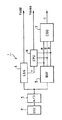
図1に、本発明のY/C分離回路のブロック図を示す。
図に示すように、本発明のY/C分離回路は、飛越し走査用のCCD2に結合されたアナログ・ディジタルコンバータ(A/D)3と、輝度信号生成回路(LSG)4と、色信号生成手段(バッファ;BUF)5と、演算手段(CPU)6と、色差信号生成回路(CSG)7とを有する。A/Dコンバータ3は、画像信号をアナログ形式からディジタル形式に変換する論理素子等から構築される既知の回路である。輝度信号生成回路4は、画像信号を基に輝度信号Yを生成する論理回路から構成される演算手段である。バッファ5は、画像信号を基に赤、緑、青の色信号R,G,Bを生成する演算機能を実現する論理回路と、この色信号を記憶する記憶機能を実現するメモリ素子とを有する回路である。演算手段6は、輝度信号生成回路4が輝度信号Yoddを生成するタイミングの制御とバッファ5に格納された色信号R,G,Bを基に補間輝度信号Yevenを生成するマイクロプロセッサである。色差信号生成回路(CSG)7は、色信号R,G,Bを基に、色差信号Cを生成する 論理素子等から構築される既知の回路である。なおここでは、輝度信号生成回路4と演算手段6は、何れも輝度信号生成に係る構成であるため、両者を併せて、輝度信号生成手段1と呼ぶことにする。
【0007】
以上の構成の本願発明に係るY/C分離回路の動作を図2及び図3を参照して説明する。
図2は、本発明に係る第1の動作説明図である。図中(a)に、CCD2のカラ ーフィルタの配置を示す。このCCD2からは、奇数フィールドを構築するための 走査が起動した場合、まず始めにラインnを構成する行R1,R2の列C1,C2,C3,…の読出しがなされ、次にラインn+1を構成する行R3,R4の列C1,C2,C3,…の読出しがなされる。以後、奇数フィールドを構成する画像信号の全てが得られるまで2行ずつの読み出し、即ち、ラインn+2,n+3,…の読出しが継続する。読出された画像信号を基に、輝度信号生成回路4では、輝度信号Yoddを生成する。一方、バッファ5は、色信号R,G,Bの生成と同時に、この色信号の記憶する。色差信号生成回路7は、この色信号R,G,Bを用いて色差信号Cを生成する。
【0008】
ここで、奇数フィールドの輝度信号Y及び色差信号Cを生成する場合についてより詳細に説明する。nラインの輝度信号Yは、図2の(b)に示したように、Y11,Y12,Y13,…で表される。これらの輝度信号は、輝度信号生成回路4における演算、即ち、演算(Ye+Mg),(Cy+G)により算出される。一方、nラインの色信号R,G,Bは、(R11,G11,B11),(R12,G12, B12),…で表される。
【0009】
図2の(b)から明らかなように、色信号R11,G11,B11と輝度信号Y11,Y12の組合により2画素分の画像データが形成される。同様に、色信 号R12,G12,B12と輝度信号Y13,Y14の組合せ、色信号R31,G 31,R31と輝度信号Y31,Y32の組合せにより2画素分の画像データが 形成される。即ち、一組の色信号と2つの輝度信号との組合せにより、2画素分の画像データが形成される。輝度信号生成回路4が輝度信号Yoddを出力するタイミングは、演算手段6の制御により実現する。演算手段6は、CCD2の読出し タイミングに同期させて、輝度信号Yoddの出力タイミングを制御する。
【0010】
なお、通常の飛越し走査の場合、奇数フィールドを構成する走査が実施されると、次に偶数フィールドを構成する走査、即ち、ラインn′,n′+1,…を構成する読出しが実施される。しかしながら本発明のY/C分離装置は、ラインn′,n′+1,…の読出しを実施する代わりに、補間フィールドの生成を実施する。
【0011】
補間フィールドを構成する処理は、バッファ5が、先に蓄積された奇数フィールドの画像信号を基に生成した色信号R,G,Bを参照することにより実現する。即ち、輝度信号生成手段1は、バッファ5が生成した色信号を基に、輝度信号Yevenを生成する。一方、色差信号生成回路7では、色信号R,G,Bを基に色差信号Cが生成される。
【0012】
本発明において、補間フィールドの輝度信号Yevenを生成するため、先に図2の(b)に示した色信号R,G,B(R11,G11,B11,R12,G12,B12,R31,G31,B31,…)を使用する。即ち、演算手段6は、バッファ5に 記憶された奇数フィールドの色信号R,G,Bを基に、色信号Cy,Mg,Ye,Gを生成する。具体的には、図3の(a)に示すように、色信号R11,G11,B11を基に、色信号Mg11c,G12cを生成する。同様に、色信号R31,G31,B31を基に、色信号Ye21c,Cy22cを生成する。以後同様に、色信号R12,G12,B12を基に色信号Mg13c,G14cを、色信号R32,G32,B32を基に色信号Ye23c,Cy24cを生成する。
【0013】
次に、図3の(b)に示すように、演算手段6は、上述の要領で生成した色信号Cy,Mg,Ye,Gを基に、輝度信号Y21,Y22,…,Y41,Y42,…を生成する。即ち、色信号Mg11c,Ye21cを基に輝度信号Y21を、色信号G12c,Cy22cを基に輝度信号Y22を、色信号Mg13c,Ye23cを基に輝度信号Y23を生成する。これらの輝度信号は、先に図2の(b)を参照して説明した要領で、画像データ(補間フィールド用)を生成する際の輝度信号Yevenとして参照される。即ち、色信号R11,G11,B11と輝度信号Y21,Y22の組合せにより2画素分の画像データが形成される。 同様に、色信号R12,G12,B12と輝度信号Y23,Y24の組合せ、色 信号R31,G31,R31と輝度信号Y41,Y42の組合せにより2画素分 の画像データが形成される。即ち、一組の色信号と2つの輝度信号との組合せにより、2画素分の画像データが形成される。
【0014】
以上説明のように、奇数フィールドを構成する輝度信号と相違する輝度信号を有する補間フィールドを構築することができる。輝度信号が相違するということは、隣接する走査線の内容が相違することを意味する。
【0015】
なお、色差信号を生成せず、色信号を基に直接的に画像表示を実現する場合、色差信号生成手段7を介さず、バッファ5から読出した色信号を参照して直接的に画像表示を実現すればよい。
【0016】
【発明の効果】
本発明に係るY/C分離装置によると、奇数フィールドを構成する輝度信号と補間フィールドを構成する補間輝度信号とが相違するため、実質的に相違する走査線が配列されることになる。従って、同一の走査線を2回繰返した場合に比べて、垂直方向の解像度を略々2倍に向上させることができる。また、CCDが捕ら えた像に対する忠実度が向上し、動きのある像が表示画面上でずれる事態を回避できる。
【図面の簡単な説明】
【図1】 本発明のY/C分離回路のブロック図。
【図2】 本発明に係る第1の動作説明図。
【図3】 本発明に係る第2の動作説明図。
【符号の説明】
1…Y/C分離回路
2…CCD
3…アナログ・ディジタル変換器
4…輝度信号生成回路
5…バッファ
6…演算回路
7…色差信号生成回路[0001]
BACKGROUND OF THE INVENTION
The present invention relates to a Y / C separation device that generates a luminance signal and a color difference signal of a sequential scanning method based on an interlaced scanning image signal.
[0002]
[Prior art]
When a luminance signal and a color difference signal are generated based on an image signal output from an image sensor such as a CCD, a Y / C separation circuit (Y: luminance signal, C: color difference signal) is used. In addition to a circuit that simply generates a luminance signal and a color difference signal, this Y / C separation circuit has a function of receiving, for example, an interlaced scanning image signal and generating a sequential scanning luminance signal and a color difference signal. There is something. Conventionally, the conversion from the interlace scanning method to the sequential scanning method is realized, for example, by repeating the scanning of each scanning line constituting an odd field twice.
[0003]
[Problems to be solved by the invention]
If one scanning line is simply displayed repeatedly, in the case of a moving image, the image may be shifted and displayed. Repeated display of the same scanning line means that scanning lines with the same content are arranged, and there has been a problem that the resolution in the vertical direction is lowered.
The present invention has been made paying attention to the above points, and provides a Y / C separation device capable of avoiding image shift and vertical resolution reduction.
[0004]
[Means for Solving the Problems]
The Y / C separation device of the present invention, which has been made paying attention to the above points, generates a color signal based on the image signal and stores the color signal, and a luminance signal based on the image signal. A luminance signal generation unit that generates a color difference signal based on the color signal, and the luminance signal generation unit performs interpolation based on the color signal stored in the color signal generation unit. In order to generate an interpolated luminance signal corresponding to the power scanning line and construct the scanning line, the interpolated luminance signal and the color signal stored in the color signal generating means are referred to.
[0005]
According to the present invention, the contents of all the scanning lines can be made substantially different without repeating one scanning line by the configuration as described above. For this reason, it is possible to avoid the image shift and the vertical resolution reduction that occur when one scanning line is repeatedly used.
[0006]
DETAILED DESCRIPTION OF THE INVENTION
FIG. 1 shows a block diagram of the Y / C separation circuit of the present invention.
As shown in the figure, the Y / C separation circuit of the present invention includes an analog / digital converter (A / D) 3 coupled to a CCD 2 for interlace scanning, a luminance signal generation circuit (LSG) 4, and a color signal. A generation unit (buffer; BUF) 5, a calculation unit (CPU) 6, and a color difference signal generation circuit (CSG) 7 are included. The A / D converter 3 is a known circuit constructed from a logic element that converts an image signal from an analog format to a digital format. The luminance signal generation circuit 4 is an arithmetic unit that includes a logic circuit that generates a luminance signal Y based on an image signal. The buffer 5 includes a logic circuit that realizes an arithmetic function for generating red, green, and blue color signals R, G, and B based on an image signal, and a memory element that realizes a storage function for storing the color signal. Circuit. The calculation means 6 is a microprocessor that generates an interpolated luminance signal Yeven based on control of the timing at which the luminance signal generation circuit 4 generates the luminance signal Yodd and the color signals R, G, and B stored in the buffer 5. The color difference signal generation circuit (CSG) 7 is a known circuit constructed from a logic element or the like that generates a color difference signal C based on the color signals R, G, and B. Here, since both the luminance signal generation circuit 4 and the calculation unit 6 are related to the generation of the luminance signal, they are collectively referred to as the luminance
[0007]
The operation of the Y / C separation circuit according to the present invention having the above configuration will be described with reference to FIGS.
FIG. 2 is a diagram illustrating a first operation according to the present invention. In the figure, (a) shows the arrangement of color filters for CCD2. From this CCD2, when scanning for constructing an odd field is started, first the columns C1, C2, C3,... Of the rows R1, R2 constituting the line n are read, and then the line n + 1 is constituted. The columns C1, C2, C3,... Of the rows R3 and R4 to be read are read out. Thereafter, reading of two rows, that is, reading of lines n + 2, n + 3,... Continues until all of the image signals constituting the odd field are obtained. Based on the read image signal, the luminance signal generation circuit 4 generates a luminance signal Yodd. On the other hand, the buffer 5 stores the color signals simultaneously with the generation of the color signals R, G, and B. The color difference signal generation circuit 7 generates a color difference signal C using the color signals R, G, and B.
[0008]
Here, the case where the luminance signal Y and the color difference signal C in the odd field are generated will be described in more detail. The luminance signal Y of the n line is represented by Y11, Y12, Y13,... as shown in FIG. These luminance signals are calculated by calculation in the luminance signal generation circuit 4, that is, calculations (Ye + Mg) and (Cy + G). On the other hand, the color signals R, G, B of n lines are represented by (R11, G11, B11), (R12, G12, B12),.
[0009]
As apparent from FIG. 2B, image data for two pixels is formed by a combination of the color signals R11, G11, B11 and the luminance signals Y11, Y12. Similarly, image data for two pixels is formed by a combination of the color signals R12, G12, B12 and the luminance signals Y13, Y14, and a combination of the color signals R31, G31, R31 and the luminance signals Y31, Y32. That is, image data for two pixels is formed by a combination of a set of color signals and two luminance signals. The timing at which the luminance signal generation circuit 4 outputs the luminance signal Yodd is realized by the control of the calculation means 6. The arithmetic means 6 controls the output timing of the luminance signal Yodd in synchronization with the readout timing of the CCD 2.
[0010]
In the case of normal interlaced scanning, when scanning that configures odd fields is performed, scanning that configures even fields, that is, reading that configures lines n ′, n ′ + 1,. . However, instead of reading the lines n ', n' + 1,..., The Y / C separator of the present invention performs generation of an interpolation field.
[0011]
The processing that constitutes the interpolation field is realized by referring to the color signals R, G, and B generated by the buffer 5 based on the image signals of the odd field accumulated previously . Immediate Chi, luminance signal generation means 1, based on the color signal buffer 5 is generated, and generates a luminance signal Yeven. On the other hand, the color difference signal generation circuit 7 generates a color difference signal C based on the color signals R, G, and B.
[0012]
In the present invention, in order to generate the luminance signal Yeven of the interpolation field, the color signals R, G, B (R11, G11, B11, R12, G12, B12, R31, G31, previously shown in FIG. B31, ...) is used. That is, the arithmetic means 6 generates the color signals Cy, Mg, Ye, G based on the odd-field color signals R, G, B stored in the buffer 5. Specifically, as shown in FIG. 3A, color signals Mg11c and G12c are generated based on the color signals R11, G11, and B11. Similarly, color signals Ye21c and Cy22c are generated based on the color signals R31, G31, and B31. Similarly thereafter, the color signals R12, G12, B12 based on the color signals Mg13c, the G14c, color signals R32, G32, B32 based on the color signals Ye23c, to produce a C y24c.
[0013]
Next, as shown in FIG. 3B, the calculation means 6 uses the luminance signals Y21, Y22,..., Y41, Y42, Y, based on the color signals Cy, Mg, Ye, G generated as described above. ... is generated. That is, the luminance signal Y21 is generated based on the color signals Mg11c and Ye21c, the luminance signal Y22 is generated based on the color signals G12c and Cy22c, and the luminance signal Y23 is generated based on the color signals Mg13c and Ye23c. These luminance signals are referred to as the luminance signal Yeven when generating the image data (for the interpolation field) in the manner described above with reference to FIG. That is, image data for two pixels is formed by the combination of the color signals R11, G11, B11 and the luminance signals Y21, Y22. Similarly, image data for two pixels is formed by a combination of the color signals R12, G12, B12 and the luminance signals Y23, Y24, and a combination of the color signals R31, G31, R31 and the luminance signals Y41, Y42. That is, image data for two pixels is formed by a combination of a set of color signals and two luminance signals.
[0014]
Above described manner, it is possible to construct interpolated field having a luminance signal and a luminance signal for phase differences that constitute the odd field. The difference in luminance signal means that the contents of adjacent scanning lines are different.
[0015]
In addition, when the image display is directly realized based on the color signal without generating the color difference signal, the image display is directly performed with reference to the color signal read from the buffer 5 without using the color difference signal generation unit 7. Realize it.
[0016]
【The invention's effect】
According to the Y / C separation device of the present invention, since the luminance signal constituting the odd field is different from the interpolation luminance signal constituting the interpolation field, substantially different scanning lines are arranged. Therefore, the vertical resolution can be improved approximately twice as compared with the case where the same scanning line is repeated twice. In addition, fidelity to images captured by the CCD is improved, and it is possible to avoid a situation in which a moving image shifts on the display screen.
[Brief description of the drawings]
FIG. 1 is a block diagram of a Y / C separation circuit of the present invention.
FIG. 2 is a diagram illustrating a first operation according to the present invention.
FIG. 3 is a diagram illustrating a second operation according to the present invention.
[Explanation of symbols]
1 ... Y / C separation circuit 2 ... CCD
DESCRIPTION OF SYMBOLS 3 ... Analog-digital converter 4 ... Luminance signal generation circuit 5 ... Buffer 6 ... Arithmetic circuit 7 ... Color difference signal generation circuit
Claims (4)
飛越し走査方式の画像信号を基に色信号を生成し、当該色信号を記憶する色信号生成手段と、
前記入力画像信号を基に第1の輝度信号を生成する輝度信号生成手段と、
前記色信号を基に色差信号を生成する色差信号生成手段とを有し、
前記輝度信号生成手段は、前記色信号生成手段に記憶された色信号を基に、前記第1の輝度信号の走査間に補間すべき走査線に対応する補間輝度信号を第2の輝度信号として生成する、
Y/C分離装置。Based on the image signal in carry over scanning method, a Y / C separation apparatus for generating a luminance signal and color difference signal of the image signal of the progressive scan method,
Generating color signals based on the image signal of the interlaced scanning method, and a color signal generating means for storing those the color signal,
Luminance signal generating means for generating a first luminance signal based on the input image signal;
Color difference signal generating means for generating a color difference signal based on the color signal;
The luminance signal generation means uses , as a second luminance signal, an interpolation luminance signal corresponding to a scanning line to be interpolated between scans of the first luminance signal , based on the color signal stored in the color signal generation means. Generate ,
Y / C separator.
飛越し走査方式の原画像信号を出力するCCD素子と、 A CCD element for outputting an interlaced scanning original image signal;
前記原画像信号を基に色信号を生成し当該色信号を記憶する色信号生成手段、前記原画像信号を基に第1の輝度信号を生成する輝度信号生成手段、及び前記色信号を基に色差信号を生成する色差信号生成手段を含むY/C分離回路とを有し、 Color signal generating means for generating a color signal based on the original image signal and storing the color signal, luminance signal generating means for generating a first luminance signal based on the original image signal, and based on the color signal Y / C separation circuit including color difference signal generation means for generating a color difference signal,
前記輝度信号生成手段は、前記色信号生成手段に記憶された色信号を基に、前記第1の輝度信号の走査間に補間すべき走査線に対応する第2の輝度信号として用いるよう補間輝度信号を生成する、 The luminance signal generation means is an interpolation luminance that is used as a second luminance signal corresponding to a scanning line to be interpolated between scans of the first luminance signal based on the color signal stored in the color signal generation means. Generate signal,
撮像装置。Imaging device.
Priority Applications (4)
| Application Number | Priority Date | Filing Date | Title |
|---|---|---|---|
| JP30746296A JP3836198B2 (en) | 1996-10-31 | 1996-10-31 | Y / C separator |
| EP97203349A EP0840527B1 (en) | 1996-10-31 | 1997-10-28 | Y/C separator |
| DE69714188T DE69714188T2 (en) | 1996-10-31 | 1997-10-28 | Y / C separator |
| US08/961,417 US6266101B1 (en) | 1996-10-31 | 1997-10-30 | Y/C separator |
Applications Claiming Priority (1)
| Application Number | Priority Date | Filing Date | Title |
|---|---|---|---|
| JP30746296A JP3836198B2 (en) | 1996-10-31 | 1996-10-31 | Y / C separator |
Publications (2)
| Publication Number | Publication Date |
|---|---|
| JPH10136393A JPH10136393A (en) | 1998-05-22 |
| JP3836198B2 true JP3836198B2 (en) | 2006-10-18 |
Family
ID=17969370
Family Applications (1)
| Application Number | Title | Priority Date | Filing Date |
|---|---|---|---|
| JP30746296A Expired - Fee Related JP3836198B2 (en) | 1996-10-31 | 1996-10-31 | Y / C separator |
Country Status (4)
| Country | Link |
|---|---|
| US (1) | US6266101B1 (en) |
| EP (1) | EP0840527B1 (en) |
| JP (1) | JP3836198B2 (en) |
| DE (1) | DE69714188T2 (en) |
Families Citing this family (3)
| Publication number | Priority date | Publication date | Assignee | Title |
|---|---|---|---|---|
| US6538694B1 (en) * | 1997-12-04 | 2003-03-25 | Victor Company Of Japan, Limited | Image pickup apparatus equipped with compatible-with-zooming type contour compensation circuit, compatible-with-image-pickup-conditions type image output circuit, and compatible-with-all-pixel-readout-system-solid-image-pickup-element type electronic zoom circuit |
| JP2002142149A (en) * | 2000-11-06 | 2002-05-17 | Mega Chips Corp | Picture processing circuit |
| US7483037B2 (en) * | 2005-10-27 | 2009-01-27 | Apple, Inc. | Resampling chroma video using a programmable graphics processing unit to provide improved color rendering |
Family Cites Families (16)
| Publication number | Priority date | Publication date | Assignee | Title |
|---|---|---|---|---|
| US4558347A (en) * | 1983-08-26 | 1985-12-10 | Rca Corporation | Progressive scan television system employing vertical detail enhancement |
| US4672445A (en) * | 1985-05-29 | 1987-06-09 | Rca Corporation | Progressive scan processor employing interpolation in luminance channel controlled by a motion signal and a vertical detail representative signal |
| US5018006A (en) * | 1985-10-31 | 1991-05-21 | Canon Kabushiki Kaisha | Multi-plate type image pickup apparatus having picture elements for producing color and luminance signals |
| US4903122A (en) * | 1987-01-28 | 1990-02-20 | Hitachi, Ltd. | Solid-state color imaging apparatus for extended definition television (EDTV) |
| JP2872759B2 (en) * | 1989-06-08 | 1999-03-24 | 富士写真フイルム株式会社 | Solid-state imaging system |
| JPH0720256B2 (en) * | 1989-06-26 | 1995-03-06 | 三洋電機株式会社 | Luminance signal separation circuit |
| US5223920A (en) * | 1991-10-03 | 1993-06-29 | Zenith Electronics Corporation | Video processor having automatic chrominance control compensation |
| JP3528184B2 (en) * | 1991-10-31 | 2004-05-17 | ソニー株式会社 | Image signal luminance correction apparatus and luminance correction method |
| EP0554035B1 (en) * | 1992-01-27 | 2001-10-17 | Mitsubishi Denki Kabushiki Kaisha | Solid state color video camera |
| KR0146260B1 (en) * | 1993-06-16 | 1998-09-15 | 모리시타 요이찌 | Solid state image pick-up apparatus |
| US5374955A (en) * | 1993-12-03 | 1994-12-20 | Hitachi, Ltd. | High-definition imaging device, and apparatuses for recording and playing back high-definition picture information |
| US5831673A (en) * | 1994-01-25 | 1998-11-03 | Przyborski; Glenn B. | Method and apparatus for storing and displaying images provided by a video signal that emulates the look of motion picture film |
| JP3216395B2 (en) * | 1994-02-25 | 2001-10-09 | 松下電器産業株式会社 | Y / C separation device |
| JP3408316B2 (en) * | 1994-04-18 | 2003-05-19 | 日本フィリップス株式会社 | Knee circuit |
| JPH0937298A (en) * | 1995-07-13 | 1997-02-07 | Philips Japan Ltd | Sequential scanning converter |
| US5663759A (en) * | 1996-06-10 | 1997-09-02 | Industrial Technology Research Institute | Feature processor for a digital camera |
-
1996
- 1996-10-31 JP JP30746296A patent/JP3836198B2/en not_active Expired - Fee Related
-
1997
- 1997-10-28 EP EP97203349A patent/EP0840527B1/en not_active Expired - Lifetime
- 1997-10-28 DE DE69714188T patent/DE69714188T2/en not_active Expired - Fee Related
- 1997-10-30 US US08/961,417 patent/US6266101B1/en not_active Expired - Lifetime
Also Published As
| Publication number | Publication date |
|---|---|
| DE69714188D1 (en) | 2002-08-29 |
| EP0840527A2 (en) | 1998-05-06 |
| DE69714188T2 (en) | 2003-04-03 |
| EP0840527A3 (en) | 2000-03-29 |
| JPH10136393A (en) | 1998-05-22 |
| US6266101B1 (en) | 2001-07-24 |
| EP0840527B1 (en) | 2002-07-24 |
Similar Documents
| Publication | Publication Date | Title |
|---|---|---|
| JP3991543B2 (en) | Imaging device | |
| JP5053654B2 (en) | Image processing apparatus and method and electronic camera | |
| US5657082A (en) | Imaging apparatus and method using interpolation processing | |
| JP3429061B2 (en) | Electronic still camera | |
| JP4555775B2 (en) | Imaging device | |
| JP2009246465A (en) | Image pickup apparatus, image pickup module and image pickup system | |
| JP3854662B2 (en) | Imaging device | |
| JP3902525B2 (en) | Image signal processing device | |
| JP3836198B2 (en) | Y / C separator | |
| JP2004336608A (en) | Method and circuit for converting image data, and electronic camera | |
| JP2004147093A (en) | Apparatus and method for signal processing, and imaging apparatus | |
| JP3123415B2 (en) | Single-chip color solid-state imaging device | |
| JP3909930B2 (en) | Single plate color solid-state imaging device | |
| WO2011061891A1 (en) | Imaging device | |
| JP3651477B2 (en) | Image signal processing device | |
| JP3134513B2 (en) | Imaging device with horizontal line interpolation function | |
| JP4475936B2 (en) | Electronic endoscope device | |
| JP3734104B2 (en) | Image signal processing device | |
| JP4059837B2 (en) | Still image color camera device | |
| JP2004147094A (en) | Signal processing device and method therefor, and imaging device | |
| JP4945852B2 (en) | Method and apparatus for generating captured image in single-plate color digital camera, digital camera, portable digital information apparatus, and digital video printer | |
| JP2899298B2 (en) | Electronic still camera system | |
| JPH08256345A (en) | Image pickup device and image signal processor | |
| JP3630821B2 (en) | Motion vector detection apparatus and method | |
| JP2000261817A (en) | Image pickup device |
Legal Events
| Date | Code | Title | Description |
|---|---|---|---|
| A711 | Notification of change in applicant |
Free format text: JAPANESE INTERMEDIATE CODE: A712 Effective date: 20050809 |
|
| A977 | Report on retrieval |
Free format text: JAPANESE INTERMEDIATE CODE: A971007 Effective date: 20060623 |
|
| TRDD | Decision of grant or rejection written | ||
| A01 | Written decision to grant a patent or to grant a registration (utility model) |
Free format text: JAPANESE INTERMEDIATE CODE: A01 Effective date: 20060629 |
|
| A61 | First payment of annual fees (during grant procedure) |
Free format text: JAPANESE INTERMEDIATE CODE: A61 Effective date: 20060726 |
|
| R150 | Certificate of patent or registration of utility model |
Free format text: JAPANESE INTERMEDIATE CODE: R150 |
|
| FPAY | Renewal fee payment (event date is renewal date of database) |
Free format text: PAYMENT UNTIL: 20090804 Year of fee payment: 3 |
|
| S111 | Request for change of ownership or part of ownership |
Free format text: JAPANESE INTERMEDIATE CODE: R313113 |
|
| FPAY | Renewal fee payment (event date is renewal date of database) |
Free format text: PAYMENT UNTIL: 20090804 Year of fee payment: 3 |
|
| R350 | Written notification of registration of transfer |
Free format text: JAPANESE INTERMEDIATE CODE: R350 |
|
| FPAY | Renewal fee payment (event date is renewal date of database) |
Free format text: PAYMENT UNTIL: 20090804 Year of fee payment: 3 |
|
| FPAY | Renewal fee payment (event date is renewal date of database) |
Free format text: PAYMENT UNTIL: 20100804 Year of fee payment: 4 |
|
| FPAY | Renewal fee payment (event date is renewal date of database) |
Free format text: PAYMENT UNTIL: 20100804 Year of fee payment: 4 |
|
| FPAY | Renewal fee payment (event date is renewal date of database) |
Free format text: PAYMENT UNTIL: 20110804 Year of fee payment: 5 |
|
| FPAY | Renewal fee payment (event date is renewal date of database) |
Free format text: PAYMENT UNTIL: 20110804 Year of fee payment: 5 |
|
| FPAY | Renewal fee payment (event date is renewal date of database) |
Free format text: PAYMENT UNTIL: 20110804 Year of fee payment: 5 |
|
| FPAY | Renewal fee payment (event date is renewal date of database) |
Free format text: PAYMENT UNTIL: 20120804 Year of fee payment: 6 |
|
| FPAY | Renewal fee payment (event date is renewal date of database) |
Free format text: PAYMENT UNTIL: 20120804 Year of fee payment: 6 |
|
| S111 | Request for change of ownership or part of ownership |
Free format text: JAPANESE INTERMEDIATE CODE: R313113 |
|
| FPAY | Renewal fee payment (event date is renewal date of database) |
Free format text: PAYMENT UNTIL: 20120804 Year of fee payment: 6 |
|
| R350 | Written notification of registration of transfer |
Free format text: JAPANESE INTERMEDIATE CODE: R350 |
|
| FPAY | Renewal fee payment (event date is renewal date of database) |
Free format text: PAYMENT UNTIL: 20120804 Year of fee payment: 6 |
|
| FPAY | Renewal fee payment (event date is renewal date of database) |
Free format text: PAYMENT UNTIL: 20130804 Year of fee payment: 7 |
|
| R250 | Receipt of annual fees |
Free format text: JAPANESE INTERMEDIATE CODE: R250 |
|
| R250 | Receipt of annual fees |
Free format text: JAPANESE INTERMEDIATE CODE: R250 |
|
| LAPS | Cancellation because of no payment of annual fees |