JP3833552B2 - Optical transceiver circuit board and optical transceiver module - Google Patents
Optical transceiver circuit board and optical transceiver module Download PDFInfo
- Publication number
- JP3833552B2 JP3833552B2 JP2002061126A JP2002061126A JP3833552B2 JP 3833552 B2 JP3833552 B2 JP 3833552B2 JP 2002061126 A JP2002061126 A JP 2002061126A JP 2002061126 A JP2002061126 A JP 2002061126A JP 3833552 B2 JP3833552 B2 JP 3833552B2
- Authority
- JP
- Japan
- Prior art keywords
- optical
- reception
- transmission
- circuit
- optical transmission
- Prior art date
- Legal status (The legal status is an assumption and is not a legal conclusion. Google has not performed a legal analysis and makes no representation as to the accuracy of the status listed.)
- Expired - Fee Related
Links
Images


Landscapes
- Optical Communication System (AREA)
- Optical Couplings Of Light Guides (AREA)
- Noise Elimination (AREA)
- Structure Of Printed Boards (AREA)
- Semiconductor Lasers (AREA)
- Light Receiving Elements (AREA)
Description
【0001】
【発明の属する技術分野】
本発明は、光ファイバ通信などの光伝送システムに用いられる光送受信モジュール、およびそのモジュールに組み込まれている光送受信回路基板に関するものである。
【0002】
【従来の技術】
光送受信モジュールは、電気信号を光信号に変換して送信する手段と光信号を電気信号に変換して受信する手段とを組み合わせて光信号の送受信を同時に行なう機器であり、光伝送システムにおける1つの重要な要素となっている。例えば光ファイバによる光伝送通信方式においては、複数の光送受信モジュール間にて光を信号として送信および受信することにより、双方向での通信が可能になる。
【0003】
例えば、光LAN(Local Area Network)に用いられる光送受信モジュールは、パーソナルコンピュータやアダプタボード等に搭載されている。また、家庭内での電子機器のネットワークなどに光ファイバを用いるシステムも提案されており、このシステムを実現するために、光送受信モジュールが家庭用の各電子機器に実際に搭載されようとしている。従来の光送受信モジュールとしては、送信用と受信用との2本のガラス製光ファイバ(以下、GOFと略称する)を接続する構成が一般的である。
【0004】
一方、光ファイバとしては、長距離伝送に使用される上記GOF以外に、プラスチック光ファイバ(以下、POFと略称する)がある。このPOFは、GOFと比べて低価格であるため、家庭内やオフィス内において大容量の情報を伝送するのに極めて有望である。また、家庭内ネットワークでは複雑な敷設作業を省くといった観点からPOFの大口径化が進み、現在では約1mm径程度のものが汎用化されている。これにより、POFでは、GOFに比べて光送信素子から光を入射させるのが容易になっている。
【0005】
さらに、こうしたPOF技術の進展に伴い、従来、送信用と受信用の2本の光ファイバにて行われている送受信を、1本のPOFにて行なう方式(1芯方式)の技術開発が進められている。
【0006】
また、光伝送システムにおいては、今日の伝送すべき情報量の増大に伴い、伝送信号の高速化が進められている。特に、伝送すべきデジタル信号のビットレートの増大は、光送受信モジュールにおける光送信素子および光受信素子の高帯域化、並びに高周波の伝送が可能な送信回路および受信回路を必要としている。
【0007】
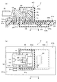
しかしながら、上記素子や回路の高帯域化は、それら素子や回路内部でのノイズを増大させることになるため、ノイズの低減などの工夫が必要となる。さらに、光送受信モジュールでは、送信部と受信部とが混載されているため、伝導ノイズや放射ノイズなどのクロストーク(混信)の影響により、誤動作を引き起こしてしまう可能性がある。そこで、従来の光送受信モジュールでは、上記クロストークを低減するための工夫がなされている。ここで、従来の光送受信モジュールの一例を図12(a)〜(c)に示す。この光送受信モジュール101は、長距離伝送に使用される2芯方式対応のものである。
【0008】
光送受信モジュール101では、光信号の送受信のために2本のGOF102を使用し、そのうちの1本は光受信部111と接続され、他の1本は光送信部112と接続される。これら光受信部111および光送信部112は、共に複数のリード線113を介して同一の光送受信回路基板114上に搭載されている。上記リード線113は、電気信号の入出力や電源線、接地線などの役割を果たしている。
【0009】
光送受信回路基板114には、その中央部に光送受信回路基板114を直線状に貫通したスリット114cが形成されており、光送受信回路基板114の領域は、上記スリット114cにより、光受信部111および光受信信号再生用IC115を有する光受信側領域114aと光送信部112および光送信素子駆動用IC116を有する光送信側領域114bとにほぼ分離されている。光送受信モジュール101では、このように光送受信回路基板114をスリット114cにて光受信側領域114a(受信回路)と光送信側領域114b(送信回路)とにほぼ分離することにより、受信回路と送信回路との間でのクロストークを低減するようにしている。
【0010】
光送受信モジュールは、上記のように、光送受信回路基板となるプリント基板に光受信部および光送信部を構成する光素子および光送受信回路部品を設けたものである。このような光送受信モジュールでは、ノイズ対策として金属製のシールドカバーにてプリント基板の所定の部分を覆った構造が多用されている。この構造の場合には、プリント基板の内部に設けられたグランド層を一部露出させ、この露出部が上記シールドカバーと電気的に接続されることにより、ノイズを適切に遮蔽することができるようになっている。
【0011】
また、特開平9−232790号公報には、ノイズ対策等をシールドカバーを使用することなく行なう構成が提案されている。その構成は、プリント基板上に形成された2つの回路間をグランドパターンを工夫することによりシールドし、2つの回路間での不要信号成分の輻射や混入あるいは回路間のクロストークを防止するようにしている。
【0012】
具体的には、同一のプリント基板上に形成される回路がシールド回路部とそれ以外の他の回路部とに区分されている。プリント基板は、少なくとも片側の面がグランドパターン面となり、このグランドパターン面が、シールド回路部に第1グランドパターン面として備えられ、他の回路部に第2グランドパターン面として備えられている。これら第1グランドパターン面と第2グランドパターン面との境界部分では、グランドパターンが除去された領域(スリット部)が形成されている。さらに、第1グランドパターン面と第2グランドパターン面との接続は、シールド回路部と他の回路部との間の入出力部により行なわれている。
【0013】
上記の構成では、金属ケースや金属板等のシールドカバーが不要となり、部品コストや製造工程の削減および機器の小型化が可能となり、かつ調整保守も容易である。
【0014】
【発明が解決しようとする課題】
ところが、上記従来の構成では、光送受信モジュールの小型化に伴い、光送信側の素子や回路と光受信側の素子や回路との距離が接近した場合には、両者間でのクロストークを十分に抑制できないという問題点を有している。
【0015】
例えば、POFを使用した1芯方式の光送受信モジュールの場合、1mm径程度のPOF端面に光送受信モジュールから光信号を入射するのは容易である。逆に、POF端面から放射されて広がる光信号を光送受信モジュールにおいて適切に受信するには、その光信号を集光する必要がある。POFを使用した1芯方式における小型化が可能な利点を考慮した場合、1芯方式対応の光送受信モジュールにおいても、2芯方式対応の光送受信モジュール(図12(a)〜(c)参照)と同様、光送受信素子の集積化および光送受信モジュールの小型化が求められる。しかしながら、このような光送受信素子のさらなる集積化は、光送受信素子間のクロストークや送受信回路間でのクロストークの増大を招来する。
【0016】
即ち、光送受信モジュールを小型化した場合には、送信回路と受信回路との間の間隔が狭まる結果、送信回路に備えられる光送信素子駆動用ICの端子や信号配線から放射される高周波ノイズが隣接する受信回路の信号配線に影響し、S/Nの低下を招くことになる。
【0017】
また、送信回路から光送信素子への入力信号線には数mA以上の変調パルス電流が流れている。したがって、送信回路と受信回路との間の間隔が狭まった場合には、上記変調パルス電流により入力信号線周辺に形成される強いパルス磁界が隣接する光受信素子、受信回路もしくは光受信素子から受信回路への出力信号線に影響を与える。これにより、光信号の受信時におけるS/Nが低下する。
【0018】
例えば、図12(a)〜(c)に示した光送受信モジュール101のように、光受信素子を含む光受信部111および受信回路と光送信素子を含む光送信部112および送信回路とを同一プリント基板上に配した場合、送信回路と受信回路との間に単純にスリット114cにより空間を設けただけの構成では、図13に示すように、送信回路から放射されるノイズの高周波成分が受信回路側に−70dBm以上も入り込み(375MHzにおいて−68dBm,625MHzにおいて−69dBm,875MHzにおいて−63dBm)、受信信号のS/Nに影響を及ぼすことになった。即ち、上記ノイズはスリット114cの空間を介して受信回路側に伝播することがわかった。
【0019】
なお、目標とするノイズレベルを−70dBmに設定した理由は、ノイズ源がクロック信号発生源の場合、受信信号のS/Nを50dB以上にすることで通常の光ファイバ通信で達成しなければならないBER(ビット・エラー・レート)を達成できることによる。この際の最小受信信号をSとした場合の最大ノイズレベルは、クロストークの目標とするS/N=50dBから求めることができる。
【0020】
本発明は、送信回路と受信回路との間の混信を適切に防止することができる光送受信回路基板および光送受信モジュールの提供を目的としている。
【0021】
【課題を解決するための手段】
上記の課題を解決するために、本発明の光送受信回路基板は、光信号の送信回路に接続される送信回路用グランド層と光信号の受信回路に接続される受信回路用グランド層とを基板内部に備え、これら両グランド層が基板内部において電気的に分離して設けられ、前記両グランド層の間に、基板内部において前記両グランド層の対向方向と交差する面状に広がる導電層を備え、前記導電層は、前記両グランド層の対向方向と交差する面上に形成された複数の格子状の閉ループを有していることを特徴としている。
【0022】
上記の構成によれば、基板の内部において、送信回路用グランド層と受信回路用グランド層との間に、両グランド層の対向方向と交差する面状に広がる導電層を備えている。したがって、一方の回路(例えば送信回路)から他方の回路(例えば受信回路)へ伝播されようとする信号を、導電層により吸収することができる。これにより、基板に単にスリットによる空間を形成した場合と比較して、送信回路と受信回路との間の混信を適切に防止することができる。
【0023】
上記の光送受信回路基板は、前記導電層に基板厚み方向に貫通した複数の貫通孔が形成されている構成としてもよい。
【0024】
上記の構成によれば、導電層は貫通孔による閉ループを備えた構成となっている。したがって、導電層は、一方の回路(例えば送信回路)から他方の回路(例えば受信回路)への伝播信号を、上記閉ループによりさらに適切に吸収することができる。これにより、送信回路と受信回路との間の混信防止機能をさらに高めることができる。
【0025】
上記の光送受信回路基板は、前記導電層が、前記両グランド層の対向方向と交差する面上に形成された少なくとも1個の閉ループを有している構成としてもよい。
【0026】
上記の構成によれば、導電層は、送信回路用グランド層と受信回路用グランド層との対向方向と交差する面上に閉ループを有している。したがって、導電層は、一方の回路(例えば送信回路)から他方の回路(例えば受信回路)への伝播信号を、上記閉ループによりさらに適切に吸収することができる。これにより、送信回路と受信回路との間の混信防止機能をさらに高めることができる。
【0027】
上記の光送受信回路基板において、前記導電層は、基板厚み方向に並ぶ複数の層体部および基板厚み方向に延びる複数の接続部を備え、各接続部により複数の前記層体部同士が電気的に接続され、複数の前記層体部と複数の前記接続部とにより前記閉ループが形成されている構成としてもよい。
【0028】
上記の構成によれば、導電層では、複数の層体部と複数の接続部とにより格子状の閉ループを容易に形成することができる。
【0029】
上記の光送受信回路基板において、前記接続部は、基板厚み方向に延びる貫通孔を内部に有する筒状部からなる構成としてもよい。
【0030】
上記の構成によれば、導電層では、複数の層体部と複数の接続部とによる、送信回路用グランド層と受信回路用グランド層との対向方向と交差する面上の閉ループと、筒状部による、前記閉ループとは異なる向きの閉ループとを備えることができる。したがって、これら互いに異なる向きの閉ループにより、送信回路と受信回路との間の混信防止機能をさらに高めることができる。
【0031】
上記の光送受信回路基板は、前記送信回路用グランド層と受信回路用グランド層と導電層とが基板の外面側において互いに接続されている構成としてもよい。
【0032】
上記の構成によれば、導電層はグランド層を介して接地されることになるので、浮遊状態となっている場合と比較して、送信回路と受信回路との間の伝播信号をさらに適切に吸収することができる。
【0033】
本発明の光送受信モジュールは、前記の何れか一つの光送受信回路基板を備えるとともに、この光送受信回路基板上における、前記導電層により区分けされた送信回路用グランド層側の領域に、光送信素子およびこの光送信素子が接続された送信回路の構成要素を備える一方、受信回路用グランド層側の領域に、光受信素子およびこの光受信素子が接続された受信回路の構成要素を備えていることを特徴としている。
【0034】
上記の構成によれば、光送受信モジュールでは、前記の何れか一つの光送受信回路基板を備えることにより、送信回路と受信回路との間の混信を適切に防止することができる。上記の光送受信モジュールは、前記光送信素子と光受信素子とが前記光送受信回路基板における同一側の面に設けられ、前記光送信素子および光受信素子が配設された基板面側に、前記導電層上に設けられかつ前記導電層と電気的に接続された電磁遮蔽部材を備えている構成としてもよい。
【0035】
上記の構成によれば、光送受信回路基板の導電層に加えて、電磁遮蔽部材を備えているので、送信回路と受信回路との間の混信をさらに適切に防止することができる。
【0036】
【発明の実施の形態】
〔実施の形態1〕
本発明の実施の一形態を図1ないし図4に基づいて以下に説明する。
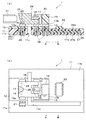
まず、本発明の前提となる光送受信モジュールの構成を縦断面図である図4(a)、平面図である図4(b)に示す。この光送受信モジュール1は、1芯方式のプラスチック光ファイバ(以下、POFと略称する)に対応するものである。
【0037】
光送受信モジュール1は、光送受信回路基板11、絶縁板12、金属マウント13、光受信素子14、受信用増幅素子15、光学部品16、マウント17、光送信素子18、マウント19、フォトダイオード20、受信信号再生用IC(受信回路の構成要素)21およびLD駆動用IC(送信回路の構成要素)22を備えている。
【0038】
光送受信回路基板11はガラスエポキシ樹脂から成り、内部に上下の2層を有している。これら2層のうち、上層はグランド層26であり、下層は電源層27である。グランド層26は接地されており、電源層27には電源電圧Vccが供給されている。光送受信回路基板11の表面と裏面には主な配線が形成されている。
【0039】
また、光送受信回路基板11には、上下方向に貫通した切り抜き状のスリット11cが形成され、このスリット11cを中心として一方側が受信側領域11aとなり、他方側が送信側領域11bとなっている。受信側領域11aの表面には、受信信号再生用IC21が搭載され、送信側領域11bの表面にはLD駆動用IC22が搭載されている。
【0040】
また、上記スリット11cにより、グランド層26および電源層27は、受信側領域11aに対応する受信回路用グランド層26aおよび受信回路用電源層27aと送信回路用グランド層26bおよび送信回路用電源層27bとに分離されている。
【0041】
したがって、受信回路と送信回路とは、スリット11cにより隔てられた構成となっている。この場合、スリット11cは、輻射信号の混入よりも伝導ノイズを抑制する効果がある。なお、上記受信回路は少なくとも受信信号再生用IC21を備えた受信側領域11aの電気回路であり、送信回路は少なくともLD駆動用IC22を備えた送信側領域11bの電気回路である。この点については、以下の各例においても同様である。
【0042】
光送受信回路基板11の上には、絶縁板12および金属マウント13がこの順序に積層され、金属マウント13の上には、光受信素子14、受信用増幅素子(略称、プリアンプ)15、マウント17に搭載された光送信素子18、およびマウント19に搭載されたフォトダイオード20が設けられている。これら各素子はリード線28により光送受信回路基板11と接続されている。
【0043】
絶縁板12は、例えばエポキシ樹脂の薄板からなり、光送受信回路基板11と金属マウント13との間に配置されている。この絶縁板12は、光受信素子14および光送信素子18を搭載している金属マウント13を光送受信回路基板11の上に直接配置した場合、金属マウント13が光送受信回路基板11の上面の配線とショートする可能性が高くなるので、それを防止するためのものである。
【0044】
金属マウント13は、光送受信回路基板11のスリット11cに対応する位置から、光受信素子14が設けられている側の受信用マウント13aと光送信素子18が設けられている側の送信用マウント13bとに分離されている。これは、金属マウント13を介しての光受信側と光送信側との間でのクロストークを防止するためである。
【0045】
光送信素子18は、例えばレーザダイオード(以下、LDと略称する)からなり、その熱的安定性を維持するために、熱伝導性の高いSiからなるマウント17に搭載されている。レーザダイオードの光出力は外部の温度に影響されて変化する。このため、レーザダイオードを光送信素子18として使用する場合には、平均光出力を一定にするために、通常、自動光出力制御(以下、APCと称する)回路が備えられる。このAPC回路はLD駆動用IC22に組み込まれている。
【0046】
また、APCを行なうにはLDの光量が一定かどうかをモニタする必要があり、このためにフォトダイオード20が備えられている。このフォトダイオード20は、マウント19におけるレンズ24側の側面に接着されている。
【0047】
光学部品16は、金属マウント13上において、受信用マウント13aと送信用マウント13bとに跨った状態に配されている。光学部品16は、例えばアクリルから成る成型品であり、可視光を損失無く通すことができるように透明となっており、レンズ24および集光ミラー25を備えている。また、光学部品16は、図1(a)に示すPOF31の先端部を挿脱可能となっている。なお、同図においては、POF31を固定するコネクタ部分の記載が省略されている。
【0048】
光送受信モジュール1では、図1(a)に示すように、POF31の先端部が光学部品16の上記コネクタに挿入され集光ミラー25の端部近くに配置されることにより、POF31との間の光伝送が可能となる。
【0049】
上記レンズ24は、送信光を集光してPOF31に高効率に送り込むためのものである。上記集光ミラー25は、POF31から放射される受信光を集光して高効率に光受信素子14に導くためのものである。
【0050】
上記の光送受信回路基板11では、光受信素子14および受信回路と光送信素子18および送信回路とが同一の光送受信回路基板11上に設けられ、これら両者間に単にスリット114cによる空間が設けられただけの構成である。したがって、先述のように、上記両者間でのクロストークを適切に抑制することができない。
【0051】
また、光送受信回路基板11では、スリット11cがAB方向において長く形成されているので、光送受信回路基板11に反りが生じ易くなる。例えば、受信側領域11aと送信側領域11bとにおいて異なる変形が生じ易くなる。この結果、光受信素子14と光送信素子18との位置ずれが生じ、POF31と光送受信モジュール1との間の光結合効率が大きく低下することになる。
【0052】
そこで、本実施の形態の光送受信モジュールは、上記の問題点も考慮した構成としている。その光送受信モジュールの構成を縦断面図である図1(a)、平面図である図1(b)、および図1(b)における正面図である図2に示す。なお、図2にはシールド部材42を省いた状態を示している。この光送受信モジュール2は、1芯方式POFに対応するものである。
【0053】
光送受信モジュール2は、前記光送受信モジュール1の光送受信回路基板11に代わる光送受信回路基板41を備えている。この光送受信回路基板41において、LD駆動用IC22は光送受信回路基板41における送信側領域41bの裏面に設けられている。
【0054】
光送受信回路基板41は前記受信側領域11aおよび送信側領域11bに対応する受信側領域41aおよび送信側領域41bを有する。受信側領域41aには、受信側要素としての、光受信素子14、受信用増幅素子15、受信信号再生用IC21および集光ミラー25等が設けられ、受信側領域41aには、送信側要素としての、光送信素子18、フォトダイオード20、LD駆動用IC22およびレンズ24等が設けられている。
【0055】
前記光送受信回路基板11のスリット11cは、光受信素子14と光送信素子18とが並ぶ方向、言い換えると、グランド層26および電源層27が分離されている方向、即ちAB方向において、このAB方向に送信用マウント13bと並んだLD駆動用IC22の位置以上の長さを有するように形成されていた。これに対して、光送受信回路基板41のスリット41cは、上記AB方向において、ほぼ、送信用マウント13bにおけるB方向側の端部の位置まで形成されている。即ち、スリット41cは、スリット11cよりもAB方向の長さが短くなっている。
【0056】
また、光送受信モジュール2はシールド部材42を備えている。このシールド部材42は、導電層としての機能、および電磁シールドとしての機能を有する。
【0057】
シールド部材42は、光送受信回路基板41の表面側からスリット41cを通って光送受信回路基板41の裏面側に達しており、光送受信回路基板41の表面側に設けられた表面側シールド部42aと裏面側に設けられた裏面側シールド部42bとを有している。
【0058】
表面側シールド部42aは、金属マウント13の送信用マウント13b、光学部品16におけるレンズ24側の部分、マウント17を含む光送信素子18、およびマウント19を含むフォトダイオード20を覆っている。裏面側シールド部42bは、光送受信回路基板41の裏面における、光送信素子18に対応するリード線28およびLD駆動用IC22等を覆っている。
【0059】
したがって、シールド部材42は、前記送信側要素群を覆い、これらをシールドしている。また、光送受信回路基板41では、受信回路用グランド層26aおよび受信回路用電源層27aと送信回路用グランド層26bおよび送信回路用電源層27bとの間に、表面側シールド部42a、即ち導電層が設けられた構成となっている。なお、シールド部材42は、送信側要素群に代えて、受信側要素群を覆うものであってもよい。
【0060】
上記の構成において、光送受信モジュール2では、光学部品16に接続されたPOF31から光信号を受信すると、この光信号は集光ミラー25にて集光され、光受信素子14に導かれる。光受信素子14では光信号が電気信号に変換され、この電気信号が受信信号再生用IC21にて処理され、所定の再生信号が得られる。
【0061】
一方、光信号をPOF31を通じて送信する場合には、LD駆動用IC22により、レーザダイオードからなる光送信素子18が駆動され、レーザ光からなる光信号が出力される。この光信号はレンズ24にて集光され、POF31内へ送り込まれる。また、光送信素子18の出力光量は、フォトダイオード20にて検出され、その出力に基づいてLD駆動用IC22により監視され、かつ適正となるように制御される。
【0062】
光送受信モジュール2では、受信側要素群と送信側要素群とが光送受信回路基板41上において混在しないように、それらを配置する領域、およびそれらが接続される回路領域を受信側領域41aと送信側領域41bとに分けている。ここで、一般に光送受信モジュールでは、受信回路と送信回路とにより要求される電源電圧が異なる場合がある。この場合、受信回路と送信回路とに電源電圧を供給する電源層27は、上記両回路のそれぞれに対応するもの同士が分離して設けられていることが望ましい。そこで、光送受信モジュール2では、電源層27として、互いに電気的に分離(絶縁)された受信回路用電源層27aと送信回路用電源層27bとを備えている。なお、光送受信モジュール2において、受信回路の電源電圧は3.3Vであり、送信回路の電源電圧は5Vである。
【0063】
また、光送受信モジュール2では、光送受信回路基板41のグランド層26が、受信回路と送信回路とのそれぞれに対応するように、受信回路用グランド層26aと送信回路用グランド層26bとして電気的に分離(絶縁)して設けられている。したがって、受信回路と送信回路とがグランド層26を共用した場合に生じる、伝導ノイズの高周波成分が送信回路から受信回路に混入する事態(あるいはその逆の事態)、即ちクロストークを防止することができる。
【0064】
また、上記のように、グランド層26を受信回路用グランド層26aと送信回路用グランド層26bとに分離した場合、クロストークの防止機能をさらに高めるためには、受信回路用グランド層26aと送信回路用グランド層26bとを可能な限り離して設けることが望ましい。
【0065】
しかしながら、受信回路および送信回路における光送受信回路基板41上面の配線層の面積は、光送受信回路基板41内部の受信回路用グランド層26aおよび送信回路用グランド層26bの面積に比べ小さく設計される。したがって、光送受信モジュール2を小型化するために受信回路と送信回路とを近接させた状態では、受信回路用グランド層26aと送信回路用グランド層26bとが必然的に非常に近接してしまうことにもなる。この場合には、受信回路用グランド層26aと送信回路用グランド層26bとの間の静電容量が大きくなり、両グランド層26a、26bに混入した高周波のノイズ成分が両グランド層26a、26b相互間において伝播しやすくなる。
【0066】
そこで光送受信モジュール2では、受信回路と送信回路とが最も近接する光送受信回路基板41の位置にスリット41cを形成し、かつスリット41c内にシールド部材42を挿入することにより、例えば送信回路から放射されるノイズをシールド部材42に吸収させるようにしている。このような構成により、先述のように、例えば単にスリット11cの空間のみにより受信側領域11aと送信側領域11bとが隔てられた構成や、プリント基板の一面に、シールド回路部用のグランドパターン面と他の回路部用のグランドパターン面とを隔てて形成した構成と比較して、受信回路と送信回路との間のクロストークを適切に防止することができる。
【0067】
上記のシールド部材42は、送信回路用グランド層26bと接続して接地し、受信回路用グランド層26aとは送受信回路基板41においては電気的に分離(絶縁)するのが電磁遮蔽機能機能を高める上で好ましい。即ち、シールド部材42は、電気的に浮遊した状態であっても電磁遮蔽機能が得られるものの、上記のように接地した方がその機能をより高めることができる。なお、受信回路用グランド層26aと送信回路用グランド層26bとは(あるいはシールド部材42も含めて)、光送受信回路基板41の外部において接続し接地する。
【0068】
また、シールド部材42は、平板の板状のものがスリット41cに挿入されていてもよいが、さらに電磁遮蔽機能を高めるために、光送信素子18を含む前記送信側要素群の表面側の部分を表面側シールド部42aが覆い、LD駆動用IC22を含む前記送信側要素群の裏面側の部分を裏面側シールド部42bが覆っている。これにより、光送信素子18や送信回路からの放射ノイズをシールド部材42内に閉じ込め、クロストークと確実に防止するようにしている。
【0069】
また、光送受信モジュール2では、光送信回路の受信回路用グランド層26aおよび受信回路用電源層27aと送信回路用グランド層26bおよび送信回路用電源層27bとの境界領域に特化して導電層(シールド部材42)を設けることで送信回路から受信回路への輻射混入を防止することができる。また、このような構造を光送受信回路基板41において採用することにより、光送受信モジュール2内部のクロストークを抑制することができる。
【0070】
次に、光送受信モジュール2において、受信回路と送信回路との間でのクロストークの抑制機能について調べた結果について説明する。
【0071】
クロストークの評価においては、ノイズ源を光送信素子18および送信回路とした。また、送信回路に周波数125MHzのパルス信号を入力して光送信素子18を発光させた状態にし、隣接する受信回路における未受光時の出力ノイズを調べた。その際には、送信光を光学部品16に入射する手前で遮蔽し、迷光が受信側要素に混入しないようにして評価を行った。
【0072】
上記試験の結果、光送受信モジュール2における高調波(クロストーク)は、図3に示すように、625MHzにおいて−78dBm、875MHzにおいて−80dBmとなり、何れも周波数においても目標である−70dBm以下に低下した。
これに対し、図12に示した光送受信モジュール101や図4に示した光送受信モジュール1における高調波(クロストーク)は、375MHzにおいて−68dBm、625MHzにおいて−69dBm、875MHzにおいて−63dBmであった。この結果、光送受信モジュール2では、光送受信モジュール101、1と比較して、クロストークの大幅な低減が可能であることが分かった。
【0073】
また、図12、先述の従来公報、あるいは図4に示した構成では、シールドカバーを備えていないので、100〜300MHzの周波数成分がどうしても空間的に輻射され、他方の回路に混入してしまうという問題点を有していたが、光送受信モジュール2では、シールド部材42を有しているので、このような問題が生じない。
【0074】
〔実施の形態2〕
本発明の実施の他の形態を図5ないし図11に基づいて以下に説明する。なお、説明の便宜上、前記の部材と同一の機能を有する部材には同一の符号を付記し、その説明を省略する。
【0075】
図5(a)(b)に示すように、本実施の形態の光送受信モジュール3は、前記光送受信モジュール2が備えていたシールド部材42を備えることなく、受信回路と送信回路との間の輻射混入(クロストーク)を防止可能な構成となっている。このために、光送受信モジュール3では、前記光送受信回路基板41に代えて、光送受信回路基板51を備えている。
【0076】
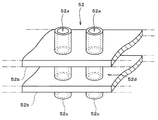
光送受信回路基板51は、図4に示した光送受信モジュール1における前述のスリット41に相当する部分に、単なる空間を形成するスリット11cに代えて、導電層52を備えている。この導電層52により、光送受信回路基板51は、受信側要素群を有する受信側領域51aと送信側要素群を有する送信側領域51bとにほぼ分けられている。また、導電層52は、光送受信回路基板51内において受信側および送信回路用グランド層26a、26b並びに受信側および送信回路用電源層27a、27bとは電気的に分離(絶縁)されている。
【0077】
導電層52は、導体により形成されていればよいものの、少なくとも1層以上の銅箔により形成されているのが好ましい。この場合、銅箔の層数は、例えば、光送受信回路基板51内に導体からなる層の数(図5(a)の例ではグランド層26と電源層27との2層)に応じて設けられる。上記銅箔層は、例えば図5(a)において52bとして示される。
【0078】
導電層52には、図5(b)におけるX−X線矢視断面図である図6、導電層52のみの斜視図である図7にも示すように、導電層52を光送受信回路基板51における表裏面の対向方向に貫通する複数個の貫通孔52aが形成されている。これら貫通孔52aにより導電層52には複数個の閉ループが形成されており、これら閉ループにより、導電層52では、入り込んできたノイズ電流を吸収するようになっている。
【0079】
また、上下方向の各銅箔層(層体部)52b同士は、上記貫通孔52aを有する例えば断面円形の筒部、即ち円筒部(接続部、筒状部)52cにより電気的に接続されている。この円筒部52cは光送受信回路基板51の表面から裏面に達している。
【0080】
なお、上記導電層52による電磁遮蔽機能は、図1(a)に示した光送受信モジュール2のシールド部材42、即ち完全導体によるものと比較した場合、同等以下となる。これは、磁界ノイズが導電層52における導体の隙間を通り抜けてしまうことによる。その反面、導電層52は、光送受信回路基板51の作製時において光送受信回路基板51に作製し易く、また、光送受信回路基板51の反り(前記スリット41cを有する場合に生じる反り)を防止できる点において有利である。
【0081】
上記の構成において、光送受信モジュール3では、導電層52の幅の分だけ受信回路用グランド層26aおよび受信回路用電源層27aと送信回路用グランド層26bおよび送信回路用電源層27bとの距離が離れることになる。また、光送受信回路基板51の内部においては、導電層52の一方側に受信回路用グランド層26aおよび受信回路用電源層27aが配置され、他方側に送信回路用グランド層26bおよび送信回路用電源層27bが配置された状態となる。したがって、光送受信モジュール3では、受信回路と送信回路との間において、高周波のノイズ成分が伝わりにくくなっている。これにより、光送受信モジュール3では、クロストークによる光伝送への悪影響が低減され、光送信素子18からPOF31への送信光の入射とPOF31から光受信素子14への受信光の入射とを確実に行なうことができるようになっている。
【0082】
次に、光送受信モジュール3におけるクロストークの防止機能について調べた結果について説明する。
【0083】
光送受信モジュール3における高調波成分(クロストーク)は、図8に示すように、625MHzにおいて−78dBm、875MHzにおいて−73dBmとなり、何れの周波数においても目標である−70dBm以下に低下した。
【0084】
これに対し、図12に示した光送受信モジュール101や図4に示した光送受信モジュール1における高調波成分(クロストーク)は、前述のように、375MHzにおいて−68dBm、625MHzにおいて−69dBm、875MHzにおいて−63dBmであった(図13参照)。この結果、光送受信モジュール3では、光送受信モジュール101、1と比較して、クロストークの大幅な低減が可能であることが分かった。
【0085】
なお、上記の例では、光送受信回路基板51において導電層52が接地されていない場合について示した。この場合には、光送受信回路基板51内部における受信回路側の配線層と送信回路側の配線層、即ちここでは受信回路用グランド層26aおよび受信回路用電源層27aと送信回路用グランド層26bおよび送信回路用電源層27bとが互いに近接していると、受信側と送信側との間で高周波のノイズ成分が伝わることも考えられる。そこで、導電層52は例えば送信回路用グランド層26bと接続して接地してもよい。
【0086】
上記のように導電層52を接地した場合における高周波のノイズ成分の伝播(クロストーク)防止機能について調べたところ、図3に示す結果となり、高周波のノイズ成分の伝播をさらに抑制することができた。すなわち、875MHzにおいて高調波成分が−73dBmから−80dBmまで低下した。
【0087】
また、光送受信回路基板51に導電層52が設けられていることは、光送受信回路基板51内部における受信回路側の配線層と送信回路側の配線層との間において伝わろうとうするノイズ成分の吸収に有効であるばかりでなく、下記の利点もある。即ち、導電層52の各銅箔層52b同士を接続している円筒部52cがアンテナとなり、導電層52では、光送受信回路基板51内部にて発信された電磁波を適切に吸収することができ、また、電磁波を発振する場合にも円筒部52cをアンテナとして利用できる。例えば、光送受信回路基板51の内部において、各層に平行な方向に電磁波が伝播するような状況が生じた場合、導電層52はその電磁波を円筒部52cにより適切に捉えて吸収することができる。
【0088】
また、導電層52では、図6および図7に示すように、導体である銅箔層52bと円筒部52cとにより複数の格子が形成されている。即ち、導電層52では、上記格子により複数の閉ループ52dが形成され、複数の銅箔層52b同士が円筒部52cにより互いに接続像されている。したがって、回路の配線につながっている貫通孔52aにて発振が生じ、その信号が光送受信回路基板51の面に平行な方向へ放射された場合に、その放射信号を閉ループ52dにて吸収することができる。
【0089】
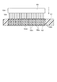
また、光送受信回路基板51は、前記導電層52に加えて、図9(a)(b)および図10に示すように、シールド板(電磁遮蔽部材)53を備えた構成としてもよい。このシールド板53は導電性材料からなり、板状の本体部53aと複数のピン53bとを備えている。本体部53aは、導電層52の銅箔層52bの長さを有し、かつ銅箔層52bの形状に沿った形状を有する。ピン53bは、本体部53aの下面から下方に延びており、導電層52の各貫通孔52aに対応して設けられている。このシールド板53は、ピン53bが導電層52の貫通孔52aに挿入されることにより光送受信回路基板51に取り付けられている。
【0090】
また、光送受信回路基板51に導電層52とシールド板53とを設ける形態は、上記のものに限定されない。例えば、導電層52は円筒部52cを有することなく、銅箔層52bに開口部が形成され、この開口部にシールド板53のピン53bを差し込むことにより、シールド板53を取り付けるものであってもよい。
【0091】
円筒部52cを有する導電層52のみを備えた図5(a)(b)に示す光送受信回路基板51の構成では、複数の貫通孔52aにて生じた発振信号を十分に吸収しきれない場合も考えられる。これに対し、導電層52に加えてシールド部材53を備えた図9(a)(b)に示す光送受信回路基板51の構成では、貫通孔52aに代えてピン53aが設けられ、さらに本体部53aが設けられていることにより、電磁波を完全に遮蔽することができる。このシールド部材53を備えた光送受信回路基板51では、図1(a)(b)に示したシールドカバー形態のシールド部材42を備えた光送受信回路基板11と同程度の電磁遮蔽機能(クロストーク防止機能)を得ることができる。
【0092】
上記の導電層52を備えた構成、並びに導電層52およびシールド板53を備えた構成は、図11(a)〜(c)に示すように、GOF(ガラス製光ファイバ)32を使用した2芯方式対応の光送受信モジュール5にも適用可能である。
【0093】
光送受信モジュール5では、光信号の送受信のために2本のGOF32を使用し、そのうちの1本は光受信部71と接続され、他の1本は光送信部72と接続される。これら光受信部71および光送信部72は、共に複数のリード線73を介して同一の光送受信回路基板74上に搭載されている。
【0094】
光送受信回路基板74には、その中央部に前記導電層52が直線状に形成されている。光送受信回路基板74の領域は、上記導電層52により、光受信部71および受信波形再生用IC(受信用IC)21を有する光受信側領域74aと光送信部72およびLD駆動用IC(送信用IC)22を有する光送信側領域74bとにほぼ分離されている。また、上記導電層52には、必要に応じて平板状のシールド板53が取り付けられる。
【0095】
上記光送受信回路基板74では、閉ループ52dを有する導電層52により、あるいは閉ループ52dを有する導電層52およびシールド板53により、光受信側領域74aと光送信側領域74bとの間、即ち受信回路と送信回路との間でのクロストークを低減することができる。
【0096】
なお、上記の各光送受信回路基板においては、導電層52を設ける代わりに、例えば図4(a)(b)に示したようなスリット(スリット11c)を形成し、このスリットの側面に導体を設けることも考えられる。しかしながら、この場合には、光送受信回路基板の作製が難しく、また光送受信回路基板の前述の反りや変形といった問題が生じる。
【0097】
また、上記問題点を解消するために、スリットを完全に導体で埋め込んでしまうことも考えられるが、このような構成は、側面に導体が設けられていない状態のスリットに、単に遮蔽板を挿入するといった構成と比べて高コストになるのが難点である。
【0098】
上記のように、本実施の形態の光送受信回路基板51、74では、少なくとも、光送受信回路基板51、74の内部における光受信側領域と光送信側領域との間に、導電層52により格子(閉ループ52d)を有する構成であるから、受信回路(光受信側領域)と送信回路(光送信側領域)との間の磁波遮蔽機能を備えることができる。これにより、受信回路と送信回路との間のクロストークは−70dBm以下に抑えられた。
【0099】
また、以上の各光送受信回路基板において、その内部に設けられている受信回路用グランド層26aおよび受信回路用電源層27aと送信回路用グランド層26bおよび送信回路用電源層27bとは、各光送受信回路基板の外面、例えば入出力部位において電気的に接続されていてもよい。このようにした場合、導電層52が電気的に浮遊状態であると、クロストークは図13に示した状態となって抑制できない場合が生じた。そこで、光送受信回路基板の外面、例えば入出力部位において導電層52を接地、即ち受信回路用グランド層26aおよび受信回路用電源層27aと接続した。これにより、クロストークを図8に示す程度のノイズレベルまで低減させることができた。
【0100】
以上のように、本光送受信モジュールでは、光送信回路から光受信回路への輻射混入や電磁誘導ノイズ、伝導ノイズといった電気的なクロストークを防止し、送信・受信回路で正常な信号処理を行なうことができる。また、クロストークの影響の少ない小型の光送受信モジュールを作製することができる。
【0101】
【発明の効果】
以上のように、本発明の光送受信回路基板は、光信号の送信回路に接続される送信回路用グランド層と光信号の受信回路に接続される受信回路用グランド層とを基板内部に備え、これら両グランド層が基板内部において電気的に分離して設けられ、前記両グランド層の間に、基板内部において前記両グランド層の対向方向と交差する面状に広がる導電層を備え、前記導電層は、前記両グランド層の対向方向と交差する面上に形成された複数の格子状の閉ループを有している構成である。
【0102】
上記の構成によれば、一方の回路(例えば送信回路)から他方の回路(例えば受信回路)へ伝播されようとする信号を、導電層により吸収することができる。これにより、基板に単にスリットによる空間を形成した場合と比較して、送信回路と受信回路との間の混信を適切に防止することができる。
【0103】
上記の光送受信回路基板は、前記導電層に基板厚み方向に貫通した複数の貫通孔が形成されている構成としてもよい。
【0104】
上記の構成によれば、導電層は、貫通孔による閉ループを備えた構成となっているので、一方の回路(例えば送信回路)から他方の回路(例えば受信回路)への伝播信号を、上記閉ループによりさらに適切に吸収することができる。これにより、送信回路と受信回路との間の混信防止機能をさらに高めることができる。
【0105】
上記の光送受信回路基板は、前記導電層が、前記両グランド層の対向方向と交差する面上に形成された少なくとも1個の閉ループを有している構成としてもよい。
【0106】
上記の構成によれば、導電層は、一方の回路(例えば送信回路)から他方の回路(例えば受信回路)への伝播信号を、閉ループによりさらに適切に吸収することができる。これにより、送信回路と受信回路との間の混信防止機能をさらに高めることができる。
【0107】
上記の光送受信回路基板において、前記導電層は、基板厚み方向に並ぶ複数の層体部および基板厚み方向に延びる複数の接続部を備え、各接続部により複数の前記層体部同士が電気的に接続され、複数の前記層体部と複数の前記接続部とにより前記閉ループが形成されている構成としてもよい。
【0108】
上記の構成によれば、導電層では、複数の層体部と複数の接続部とにより格子状の閉ループを容易に形成することができる。
【0109】
上記の光送受信回路基板において、前記接続部は、基板厚み方向に延びる貫通孔を内部に有する筒状部からなる構成としてもよい。
【0110】
上記の構成によれば、導電層では、複数の層体部と複数の接続部とによる、送信回路用グランド層と受信回路用グランド層との対向方向と交差する面上の閉ループと、筒状部による、前記閉ループとは異なる向きの閉ループとを備えることができる。したがって、これら互いに異なる向きの閉ループにより、送信回路と受信回路との間の混信防止機能をさらに高めることができる。
【0111】
上記の光送受信回路基板は、前記送信回路用グランド層と受信回路用グランド層と導電層とが基板の外面側において互いに接続されている構成としてもよい。
【0112】
上記の構成によれば、導電層はグランド層を介して接地されることになるので、浮遊状態となっている場合と比較して、送信回路と受信回路との間の伝播信号をさらに適切に吸収することができる。
【0113】
本発明の光送受信モジュールは、前記の何れか一つの光送受信回路基板を備えるとともに、この光送受信回路基板上における、前記導電層により区分けされた送信回路用グランド層側の領域に、光送信素子およびこの光送信素子が接続された送信回路の構成要素を備える一方、受信回路用グランド層側の領域に、光受信素子およびこの光受信素子が接続された受信回路の構成要素を備えている構成である。
【0114】
上記の構成によれば、光送受信モジュールでは、前記の何れか一つの光送受信回路基板を備えることにより、送信回路と受信回路との間の混信を適切に防止することができる。
上記の光送受信モジュールは、前記光送信素子と光受信素子とが前記光送受信回路基板における同一側の面に設けられ、前記光送信素子および光受信素子が配設された基板面側に、前記導電層上に設けられかつ前記導電層と電気的に接続された電磁遮蔽部材を備えている構成としてもよい。
【0115】
上記の構成によれば、光送受信回路基板の導電層に加えて、電磁遮蔽部材を備えているので、送信回路と受信回路との間の混信をさらに適切に防止することができる。
【図面の簡単な説明】
【図1】 図1(a)は、本発明の実施の一形態における1芯対応方式の光送受信モジュールを示す概略の縦断面図、図1(b)は、図1(a)に示した光送受信モジュールの平面図である。
【図2】 図1(a)に示した光送受信モジュールにおけるシールド部材を除去した状態の正面図である。
【図3】 図1(a)に示した光送受信モジュールにおけるクロストークの発生状態を示すグラフである。
【図4】 図4(a)は、本発明の前提例となる1芯対応方式の光送受信モジュールを示す概略の縦断面図、図4(b)は、図4(a)に示した光送受信モジュールの平面図である。
【図5】 図5(a)は、本発明の実施の一形態における1芯対応方式の光送受信モジュールを示す概略の縦断面図、図5(b)は、図5(a)に示した光送受信モジュールの平面図である。
【図6】 図5(b)におけるX−X線矢視断面図である。
【図7】 図5(a)に示した導電層の要部を示す斜視図である。
【図8】 図5(a)に示した光送受信モジュールにおけるクロストークの発生状態を示すグラフである。
【図9】 図9(a)は、本発明の実施の他の形態における1芯対応方式の光送受信モジュールを示す概略の縦断面図、図9(b)は、図9(a)に示した光送受信モジュールの平面図である。
【図10】 正面から見た図9(a)に示すシールド板と図9(b)における導電層のY−Y線矢視断面とを示す図である。
【図11】 図11(a)は、本発明の実施のさらに他の形態における2芯対応方式の光送受信モジュールを示す概略の正面図、図11(b)は図11(a)に示した光送受信モジュールの側面図、図11(c)は、同平面図である。
【図12】 図12(a)は、2芯対応方式における従来の光送受信モジュールの正面図、図12(b)は、図12(a)に示した光送受信モジュールの側面図、図12(c)は、図12(a)に示した光送受信モジュールの平面図である。
【図13】 図12(a)に示した光送受信モジュールにおけるクロストークの発生状態を示すグラフである。
【符号の説明】
2,3,5 光送受信モジュール
41,51 光送受信回路基板
14 光受信素子
15 受信用増幅素子
16 光学部品
18 光送信素子
20 フォトダイオード
21 受信信号再生用IC(受信回路の構成要素)
22 LD駆動用IC(送信回路の構成要素)
26 グランド層
26a 受信回路用グランド層
26b 送信回路用グランド層
27 電源層27
27a 受信回路用電源層
27b 送信回路用電源層
42 シールド部材(導電層)
51a 受信側領域
51b 送信側領域
52 導電層
52a 貫通孔
52b 銅箔層(層体部)
52c 円筒部(接続部、筒状部)
52d 閉ループ
53 シールド板(電磁遮蔽部材)
53a 本体部
53b ピン[0001]
BACKGROUND OF THE INVENTION
The present invention relates to an optical transmission / reception module used in an optical transmission system such as optical fiber communication, and an optical transmission / reception circuit board incorporated in the module.
[0002]
[Prior art]
An optical transceiver module is a device that simultaneously transmits and receives optical signals by combining means for converting electrical signals to optical signals and transmitting and means for converting optical signals to electrical signals and receiving them. It is an important factor. For example, in an optical transmission communication system using an optical fiber, bidirectional communication is possible by transmitting and receiving light as a signal between a plurality of optical transceiver modules.
[0003]
For example, an optical transmission / reception module used for an optical LAN (Local Area Network) is mounted on a personal computer, an adapter board, or the like. In addition, a system using an optical fiber for a network of electronic devices in a home has been proposed. In order to realize this system, an optical transmission / reception module is actually being installed in each home electronic device. As a conventional optical transmission / reception module, a configuration in which two glass optical fibers for transmission and reception (hereinafter abbreviated as GOF) are generally connected.
[0004]
On the other hand, as an optical fiber, there is a plastic optical fiber (hereinafter abbreviated as POF) in addition to the GOF used for long-distance transmission. Since this POF is less expensive than GOF, it is extremely promising for transmitting large volumes of information in the home or office. Further, in the home network, the POF has been increased in diameter from the viewpoint of omitting complicated laying work, and at the present time, the one having a diameter of about 1 mm is widely used. As a result, in the POF, it is easier to make light incident from the optical transmission element than in the GOF.
[0005]
Furthermore, along with the progress of such POF technology, technological development of a method (single-core method) in which transmission / reception conventionally performed by two optical fibers for transmission and reception is performed by one POF is advanced. It has been.
[0006]
In addition, in an optical transmission system, transmission signals have been increased in speed with an increase in the amount of information to be transmitted today. In particular, an increase in the bit rate of a digital signal to be transmitted requires a transmission circuit and a reception circuit capable of increasing the bandwidth of an optical transmission element and an optical reception element in an optical transmission / reception module and transmitting a high frequency.
[0007]
However, increasing the bandwidth of the elements and circuits increases noise in the elements and circuits, and thus it is necessary to devise measures such as noise reduction. Furthermore, in the optical transceiver module, since the transmitter and the receiver are mixed, there is a possibility of causing a malfunction due to the influence of crosstalk (crosstalk) such as conduction noise and radiation noise. Therefore, the conventional optical transceiver module has been devised to reduce the crosstalk. Here, an example of a conventional optical transceiver module is shown in FIGS. This
[0008]
The
[0009]
The optical transmission /
[0010]
As described above, the optical transmission / reception module is obtained by providing an optical element and an optical transmission / reception circuit component constituting an optical reception unit and an optical transmission unit on a printed circuit board serving as an optical transmission / reception circuit substrate. In such an optical transceiver module, a structure in which a predetermined portion of a printed board is covered with a metal shield cover is often used as a noise countermeasure. In the case of this structure, a part of the ground layer provided inside the printed circuit board is exposed, and the exposed portion is electrically connected to the shield cover, so that noise can be appropriately shielded. It has become.
[0011]
Japanese Patent Laid-Open No. 9-232790 proposes a configuration in which noise countermeasures are performed without using a shield cover. The configuration shields the two circuits formed on the printed circuit board by devising a ground pattern so as to prevent radiation and mixing of unnecessary signal components between the two circuits or crosstalk between the circuits. ing.
[0012]
Specifically, circuits formed on the same printed circuit board are divided into a shield circuit portion and other circuit portions. In the printed circuit board, at least one surface is a ground pattern surface, and this ground pattern surface is provided as a first ground pattern surface in the shield circuit portion, and is provided as a second ground pattern surface in the other circuit portions. At the boundary portion between the first ground pattern surface and the second ground pattern surface, a region (slit portion) from which the ground pattern is removed is formed. Further, the connection between the first ground pattern surface and the second ground pattern surface is made by an input / output unit between the shield circuit unit and another circuit unit.
[0013]
With the above-described configuration, a shield cover such as a metal case or a metal plate is not necessary, and it is possible to reduce component costs and manufacturing processes, reduce the size of the device, and facilitate adjustment and maintenance.
[0014]
[Problems to be solved by the invention]
However, with the conventional configuration described above, when the distance between the optical transmission side element or circuit and the optical reception side element or circuit approaches as the size of the optical transmission / reception module decreases, crosstalk between the two is sufficient. It has a problem that it cannot be suppressed.
[0015]
For example, in the case of a single-core type optical transmission / reception module using POF, it is easy to make an optical signal incident from the optical transmission / reception module on a POF end face having a diameter of about 1 mm. Conversely, in order for the optical transmission / reception module to properly receive the optical signal emitted from the end face of the POF, the optical signal needs to be collected. In consideration of the advantages of downsizing in the single-core method using POF, even in the single-core optical transceiver module, the two-core optical transceiver module (see FIGS. 12A to 12C) Similarly, integration of optical transceiver elements and miniaturization of optical transceiver modules are required. However, further integration of such optical transceiver elements leads to increased crosstalk between the optical transceiver elements and crosstalk between the transceiver circuits.
[0016]
That is, when the optical transmission / reception module is downsized, the interval between the transmission circuit and the reception circuit is narrowed. As a result, the high frequency noise radiated from the terminal of the optical transmission element driving IC provided in the transmission circuit and the signal wiring is reduced. This affects the signal wiring of the adjacent receiving circuit, leading to a decrease in S / N.
[0017]
Further, a modulation pulse current of several mA or more flows through the input signal line from the transmission circuit to the optical transmission element. Therefore, when the interval between the transmitting circuit and the receiving circuit is narrowed, a strong pulse magnetic field formed around the input signal line by the modulated pulse current is received from the adjacent optical receiving element, receiving circuit or optical receiving element. It affects the output signal line to the circuit. Thereby, S / N at the time of reception of an optical signal falls.
[0018]
For example, as in the
[0019]
The reason for setting the target noise level to -70 dBm must be achieved by normal optical fiber communication by setting the S / N of the received signal to 50 dB or more when the noise source is a clock signal generation source. BER (bit error rate) can be achieved. In this case, the maximum noise level when the minimum received signal is S can be obtained from S / N = 50 dB which is the target of crosstalk.
[0020]
An object of the present invention is to provide an optical transmission / reception circuit board and an optical transmission / reception module that can appropriately prevent interference between a transmission circuit and a reception circuit.
[0021]
[Means for Solving the Problems]
In order to solve the above problems, an optical transmission / reception circuit board according to the present invention includes a transmission circuit ground layer connected to an optical signal transmission circuit and a reception circuit ground layer connected to an optical signal reception circuit. Provided inside, these two ground layers are electrically separated inside the substrate, and between the two ground layers, a conductive layer extending in a plane intersecting the opposing direction of the two ground layers inside the substrate is provided. , The conductive layer has a plurality of lattice-shaped closed loops formed on a surface that intersects the opposing direction of the ground layers. It is characterized by that.
[0022]
According to the above configuration, the conductive layer extending in a plane intersecting the opposing direction of both ground layers is provided between the ground layer for the transmission circuit and the ground layer for the reception circuit inside the substrate. Therefore, a signal that is to be propagated from one circuit (for example, a transmission circuit) to the other circuit (for example, a reception circuit) can be absorbed by the conductive layer. Thereby, it is possible to appropriately prevent interference between the transmission circuit and the reception circuit as compared with a case where a space simply formed by a slit is formed on the substrate.
[0023]
The optical transmission / reception circuit board may have a configuration in which a plurality of through holes penetrating in the thickness direction of the substrate are formed in the conductive layer.
[0024]
According to said structure, the electrically conductive layer becomes a structure provided with the closed loop by a through-hole. Therefore, the conductive layer can more appropriately absorb the propagation signal from one circuit (for example, a transmission circuit) to the other circuit (for example, a reception circuit) by the closed loop. Thereby, the interference prevention function between the transmission circuit and the reception circuit can be further enhanced.
[0025]
The optical transmission / reception circuit board may have a configuration in which the conductive layer has at least one closed loop formed on a surface intersecting a facing direction of the two ground layers.
[0026]
According to said structure, the conductive layer has a closed loop on the surface which cross | intersects the opposing direction of the ground layer for transmitting circuits, and the ground layer for receiving circuits. Therefore, the conductive layer can more appropriately absorb the propagation signal from one circuit (for example, a transmission circuit) to the other circuit (for example, a reception circuit) by the closed loop. Thereby, the interference prevention function between the transmission circuit and the reception circuit can be further enhanced.
[0027]
In the optical transmission / reception circuit board, the conductive layer includes a plurality of layer body portions arranged in the substrate thickness direction and a plurality of connection portions extending in the substrate thickness direction, and the plurality of layer body portions are electrically connected to each other by the connection portions. The closed loop may be formed by a plurality of the layer body portions and a plurality of the connection portions.
[0028]
According to said structure, in a conductive layer, a lattice-like closed loop can be easily formed with a some layer body part and a some connection part.
[0029]
In the above optical transmission / reception circuit board, the connection part may be formed of a cylindrical part having a through hole extending in a thickness direction of the board.
[0030]
According to said structure, in a conductive layer, the closed loop on the surface which cross | intersects the opposing direction of the ground layer for transmitting circuits and the ground layer for receiving circuits by a several layer body part and a several connection part, and a cylindrical shape And a closed loop of a different direction from the closed loop. Therefore, the interference prevention function between the transmission circuit and the reception circuit can be further enhanced by the closed loops having different directions.
[0031]
The optical transmission / reception circuit board may be configured such that the transmission circuit ground layer, the reception circuit ground layer, and the conductive layer are connected to each other on the outer surface side of the substrate.
[0032]
According to the above configuration, since the conductive layer is grounded through the ground layer, the propagation signal between the transmission circuit and the reception circuit is more appropriately compared with the case where the conductive layer is in a floating state. Can be absorbed.
[0033]
An optical transmission / reception module according to the present invention includes any one of the optical transmission / reception circuit boards described above, and an optical transmission element is provided on a region of the optical transmission / reception circuit board on the side of the transmission circuit ground layer divided by the conductive layer. And a transmission circuit component to which the optical transmission element is connected, and an optical reception element and a reception circuit component to which the optical reception element is connected in the region on the ground layer side for the reception circuit. It is characterized by.
[0034]
According to said structure, in an optical transmission / reception module, the interference between a transmission circuit and a receiving circuit can be prevented appropriately by providing any one said optical transmission / reception circuit board. In the optical transmission / reception module, the optical transmission element and the optical reception element are provided on the same surface of the optical transmission / reception circuit board, and the optical transmission / reception module is provided on the substrate surface side on which the optical transmission element and the optical reception element are disposed It is good also as a structure provided with the electromagnetic shielding member provided on the conductive layer and electrically connected with the said conductive layer.
[0035]
According to the above configuration, since the electromagnetic shielding member is provided in addition to the conductive layer of the optical transmission / reception circuit board, it is possible to more appropriately prevent interference between the transmission circuit and the reception circuit.
[0036]
DETAILED DESCRIPTION OF THE INVENTION
[Embodiment 1]
An embodiment of the present invention will be described below with reference to FIGS.
First, FIG. 4A which is a longitudinal sectional view and FIG. 4B which is a plan view show the configuration of an optical transceiver module which is a premise of the present invention. This
[0037]
The optical transmission /
[0038]
The optical
[0039]
The optical transmission /
[0040]
The
[0041]
Therefore, the receiving circuit and the transmitting circuit are separated by the
[0042]
An insulating
[0043]
The insulating
[0044]
From the position corresponding to the
[0045]
The
[0046]
In order to perform APC, it is necessary to monitor whether the light quantity of the LD is constant. For this purpose, a
[0047]
The
[0048]
In the optical transmission /
[0049]
The
[0050]
In the optical transmission /
[0051]
Moreover, in the optical transmission /
[0052]
Therefore, the optical transceiver module of the present embodiment is configured in consideration of the above problems. The configuration of the optical transceiver module is shown in FIG. 1A, which is a longitudinal sectional view, FIG. 1B, which is a plan view, and FIG. 2, which is a front view in FIG. FIG. 2 shows a state where the
[0053]
The
[0054]
The optical transmission /
[0055]
The
[0056]
The
[0057]
The
[0058]
The
[0059]
Therefore, the
[0060]
In the above configuration, when the
[0061]
On the other hand, when transmitting an optical signal through the
[0062]
In the optical transmission /
[0063]
Further, in the
[0064]
Further, as described above, when the
[0065]
However, the area of the wiring layer on the upper surface of the optical transmission /
[0066]
Therefore, in the
[0067]
The
[0068]
Further, the
[0069]
Further, in the
[0070]
Next, the result of examining the function of suppressing crosstalk between the receiving circuit and the transmitting circuit in the
[0071]
In the evaluation of crosstalk, the noise source is the
[0072]
As a result of the above test, the harmonic (crosstalk) in the
On the other hand, the harmonics (crosstalk) in the
[0073]
Further, in the configuration shown in FIG. 12, the above-described conventional publication or FIG. 4, since the shield cover is not provided, the frequency component of 100 to 300 MHz is inevitably spatially radiated and mixed into the other circuit. However, since the
[0074]
[Embodiment 2]
Another embodiment of the present invention will be described below with reference to FIGS. For convenience of explanation, members having the same functions as those described above are denoted by the same reference numerals and description thereof is omitted.
[0075]
As shown in FIGS. 5 (a) and 5 (b), the
[0076]
The optical transmission /
[0077]
The
[0078]
As shown in FIG. 6 which is a sectional view taken along line XX in FIG. 5B and FIG. 7 which is a perspective view of only the
[0079]
Further, the copper foil layers (layer body portions) 52b in the vertical direction are electrically connected to each other by, for example, a cylindrical section having a through-
[0080]
The electromagnetic shielding function by the
[0081]
In the configuration described above, in the
[0082]
Next, the results of examining the function of preventing crosstalk in the
[0083]
As shown in FIG. 8, the harmonic component (crosstalk) in the
[0084]
On the other hand, the harmonic component (crosstalk) in the
[0085]
In the above example, the case where the
[0086]
When the
[0087]
Further, the provision of the
[0088]
In the
[0089]
In addition to the
[0090]
The form in which the
[0091]
In the configuration of the optical transmission /
[0092]
The configuration including the
[0093]
The
[0094]
The optical transmission /
[0095]
In the optical transmission /
[0096]
In each of the above optical transmission / reception circuit boards, instead of providing the
[0097]
In addition, in order to solve the above problems, it is conceivable that the slit is completely filled with a conductor. However, in such a configuration, a shielding plate is simply inserted into the slit in which no conductor is provided on the side surface. It is difficult to be expensive compared to the configuration of doing.
[0098]
As described above, in the optical transmission /
[0099]
Further, in each of the optical transmission / reception circuit boards described above, the reception
[0100]
As described above, this optical transceiver module prevents electrical crosstalk such as radiation mixing from the optical transmission circuit to the optical reception circuit, electromagnetic induction noise, and conduction noise, and performs normal signal processing in the transmission / reception circuit. be able to. In addition, a small optical transceiver module with little influence of crosstalk can be manufactured.
[0101]
【The invention's effect】
As described above, the optical transmission / reception circuit board of the present invention includes the transmission circuit ground layer connected to the optical signal transmission circuit and the reception circuit ground layer connected to the optical signal reception circuit inside the board, Both of these ground layers are provided electrically separated inside the substrate, and between the two ground layers, a conductive layer extending in a plane intersecting the opposing direction of the both ground layers inside the substrate is provided, The conductive layer has a plurality of lattice-shaped closed loops formed on a surface that intersects the opposing direction of the ground layers. It is a configuration.
[0102]
According to the above configuration, a signal that is to be propagated from one circuit (for example, a transmission circuit) to the other circuit (for example, a reception circuit) can be absorbed by the conductive layer. Thereby, it is possible to appropriately prevent interference between the transmission circuit and the reception circuit as compared with a case where a space simply formed by a slit is formed on the substrate.
[0103]
The optical transmission / reception circuit board may have a configuration in which a plurality of through holes penetrating in the thickness direction of the substrate are formed in the conductive layer.
[0104]
According to the above configuration, since the conductive layer has a configuration including a closed loop by a through hole, a propagation signal from one circuit (for example, a transmission circuit) to the other circuit (for example, a reception circuit) is transmitted to the closed loop. Can be absorbed more appropriately. Thereby, the interference prevention function between the transmission circuit and the reception circuit can be further enhanced.
[0105]
The optical transmission / reception circuit board may have a configuration in which the conductive layer has at least one closed loop formed on a surface intersecting a facing direction of the two ground layers.
[0106]
According to said structure, the conductive layer can absorb the propagation signal from one circuit (for example, transmission circuit) to the other circuit (for example, reception circuit) more appropriately by a closed loop. Thereby, the interference prevention function between the transmission circuit and the reception circuit can be further enhanced.
[0107]
In the optical transmission / reception circuit board, the conductive layer includes a plurality of layer body portions arranged in the substrate thickness direction and a plurality of connection portions extending in the substrate thickness direction, and the plurality of layer body portions are electrically connected to each other by the connection portions. The closed loop may be formed by a plurality of the layer body portions and a plurality of the connection portions.
[0108]
According to said structure, in a conductive layer, a lattice-like closed loop can be easily formed with a some layer body part and a some connection part.
[0109]
In the above optical transmission / reception circuit board, the connection part may be formed of a cylindrical part having a through hole extending in a thickness direction of the board.
[0110]
According to said structure, in a conductive layer, the closed loop on the surface which cross | intersects the opposing direction of the ground layer for transmitting circuits and the ground layer for receiving circuits by a several layer body part and a several connection part, and a cylindrical shape And a closed loop of a different direction from the closed loop. Therefore, the interference prevention function between the transmission circuit and the reception circuit can be further enhanced by the closed loops having different directions.
[0111]
The optical transmission / reception circuit board may be configured such that the transmission circuit ground layer, the reception circuit ground layer, and the conductive layer are connected to each other on the outer surface side of the substrate.
[0112]
According to the above configuration, since the conductive layer is grounded through the ground layer, the propagation signal between the transmission circuit and the reception circuit is more appropriately compared with the case where the conductive layer is in a floating state. Can be absorbed.
[0113]
An optical transmission / reception module according to the present invention includes any one of the optical transmission / reception circuit boards described above, and an optical transmission element is provided on a region of the optical transmission / reception circuit board on the side of the transmission circuit ground layer divided by the conductive layer. And a constituent element of the transmitting circuit to which the optical transmitting element is connected, and a constituent element of the receiving circuit to which the optical receiving element and the optical receiving element are connected in the region on the ground layer side for the receiving circuit. It is.
[0114]
According to said structure, in an optical transmission / reception module, the interference between a transmission circuit and a receiving circuit can be prevented appropriately by providing any one said optical transmission / reception circuit board.
In the optical transmission / reception module, the optical transmission element and the optical reception element are provided on the same surface of the optical transmission / reception circuit board, and the optical transmission / reception module is provided on the substrate surface side on which the optical transmission element and the optical reception element are disposed It is good also as a structure provided with the electromagnetic shielding member provided on the conductive layer and electrically connected with the said conductive layer.
[0115]
According to the above configuration, since the electromagnetic shielding member is provided in addition to the conductive layer of the optical transmission / reception circuit board, it is possible to more appropriately prevent interference between the transmission circuit and the reception circuit.
[Brief description of the drawings]
FIG. 1 (a) is a schematic longitudinal sectional view showing a single-core compatible optical transceiver module according to an embodiment of the present invention, and FIG. 1 (b) is shown in FIG. 1 (a). It is a top view of an optical transceiver module.
FIG. 2 is a front view showing a state where a shield member is removed from the optical transceiver module shown in FIG.
FIG. 3 is a graph showing a state of occurrence of crosstalk in the optical transceiver module shown in FIG.
4 (a) is a schematic longitudinal sectional view showing a single-core compatible optical transceiver module as a precondition of the present invention, and FIG. 4 (b) is a diagram of the light shown in FIG. 4 (a). It is a top view of a transmission / reception module.
FIG. 5 (a) is a schematic longitudinal sectional view showing a single-core compatible optical transceiver module according to an embodiment of the present invention, and FIG. 5 (b) is shown in FIG. 5 (a). It is a top view of an optical transceiver module.
6 is a cross-sectional view taken along line XX in FIG.
7 is a perspective view showing a main part of the conductive layer shown in FIG.
FIG. 8 is a graph showing a state of occurrence of crosstalk in the optical transceiver module shown in FIG.
FIG. 9 (a) is a schematic longitudinal sectional view showing a single-core compatible optical transceiver module according to another embodiment of the present invention, and FIG. 9 (b) is shown in FIG. 9 (a). It is a top view of the optical transmission / reception module.
10 is a diagram showing a shield plate shown in FIG. 9A and a cross-sectional view taken along line YY of the conductive layer in FIG. 9B, as viewed from the front.
FIG. 11 (a) is a schematic front view showing a two-core compatible optical transceiver module in still another embodiment of the present invention, and FIG. 11 (b) is shown in FIG. 11 (a). FIG. 11C is a side view of the optical transceiver module, and FIG.
12 (a) is a front view of a conventional optical transceiver module in a two-core compatible system, FIG. 12 (b) is a side view of the optical transceiver module shown in FIG. 12 (a), and FIG. FIG. 12C is a plan view of the optical transmission / reception module shown in FIG.
13 is a graph showing a state of occurrence of crosstalk in the optical transceiver module shown in FIG.
[Explanation of symbols]
2,3,5 optical transceiver module
41,51 Optical transceiver circuit board
14 Optical receiving element
15 Amplifying element for reception
16 Optical components
18 Optical transmitter
20 photodiode
21 Received signal reproduction IC (component of receiving circuit)
22 LD driver IC (component of transmission circuit)
26 Ground layer
26a Ground layer for receiving circuit
26b Ground layer for transmission circuit
27
27a Power supply layer for receiving circuit
27b Power supply layer for transmission circuit
42 Shield member (conductive layer)
51a Receiving side area
51b Transmission side area
52 Conductive layer
52a Through hole
52b Copper foil layer (layer body)
52c Cylindrical part (connecting part, cylindrical part)
52d closed loop
53 Shield plate (electromagnetic shielding member)
53a Body
53b pin
Claims (6)
前記両グランド層の間に、基板内部において前記両グランド層の対向方向と交差する面状に広がる導電層を備え、
前記導電層は、前記両グランド層の対向方向と交差する面上に形成された複数の格子状の閉ループを有していることを特徴とする光送受信回路基板。 A transmission circuit ground layer connected to the optical signal transmission circuit and a reception circuit ground layer connected to the optical signal reception circuit are provided inside the substrate, and these ground layers are electrically separated inside the substrate. Provided,
A conductive layer extending in a plane intersecting the opposing direction of the two ground layers inside the substrate between the two ground layers,
The optical transmission / reception circuit board, wherein the conductive layer has a plurality of grid-like closed loops formed on a surface intersecting with a facing direction of the ground layers.
Priority Applications (1)
| Application Number | Priority Date | Filing Date | Title |
|---|---|---|---|
| JP2002061126A JP3833552B2 (en) | 2002-03-06 | 2002-03-06 | Optical transceiver circuit board and optical transceiver module |
Applications Claiming Priority (1)
| Application Number | Priority Date | Filing Date | Title |
|---|---|---|---|
| JP2002061126A JP3833552B2 (en) | 2002-03-06 | 2002-03-06 | Optical transceiver circuit board and optical transceiver module |
Publications (2)
| Publication Number | Publication Date |
|---|---|
| JP2003264471A JP2003264471A (en) | 2003-09-19 |
| JP3833552B2 true JP3833552B2 (en) | 2006-10-11 |
Family
ID=29195664
Family Applications (1)
| Application Number | Title | Priority Date | Filing Date |
|---|---|---|---|
| JP2002061126A Expired - Fee Related JP3833552B2 (en) | 2002-03-06 | 2002-03-06 | Optical transceiver circuit board and optical transceiver module |
Country Status (1)
| Country | Link |
|---|---|
| JP (1) | JP3833552B2 (en) |
Families Citing this family (3)
| Publication number | Priority date | Publication date | Assignee | Title |
|---|---|---|---|---|
| JP5535142B2 (en) * | 2011-07-11 | 2014-07-02 | 古河電気工業株式会社 | Laser equipment |
| WO2019104560A1 (en) * | 2017-11-29 | 2019-06-06 | 深圳市大疆创新科技有限公司 | Detecting equipment and moveable platform |
| JP7466386B2 (en) | 2020-06-12 | 2024-04-12 | 株式会社デンソー | Optical transmission module and electronic control device |
-
2002
- 2002-03-06 JP JP2002061126A patent/JP3833552B2/en not_active Expired - Fee Related
Also Published As
| Publication number | Publication date |
|---|---|
| JP2003264471A (en) | 2003-09-19 |
Similar Documents
| Publication | Publication Date | Title |
|---|---|---|
| US20070058980A1 (en) | Optical transceiver suppressing radiation noise form transmitter to receiver | |
| US20080196929A1 (en) | Optical transmitter module | |
| JP2010191346A (en) | Optical module | |
| JPWO2007114384A1 (en) | Signal transmission equipment | |
| US9063310B2 (en) | Optical transceiver implementing with flexible printed circuit connecting optical subassembly to circuit board | |
| JPWO2006025523A1 (en) | Photoelectric composite module | |
| US10727953B2 (en) | Package for optical receiver module | |
| JP6988322B2 (en) | Package for optical receiver module | |
| US11372181B2 (en) | Optical module | |
| CN105339820A (en) | Optical-module member, optical module, and electronic device | |
| JP2007027507A (en) | Optical module | |
| JP3833552B2 (en) | Optical transceiver circuit board and optical transceiver module | |
| CN113970815B (en) | Optical module | |
| JP4828103B2 (en) | Optical transceiver module | |
| JP6223671B2 (en) | Optical module | |
| US6465858B2 (en) | Semiconductor device package for optical communication device | |
| US11327256B2 (en) | Optical receiver module and package for optical receiver module | |
| US20010022370A1 (en) | Transducer module with an optical semiconductor, and method for producing a transducer module | |
| US10948670B2 (en) | Optical module | |
| US6614658B2 (en) | Flexible cable stiffener for an optical transceiver | |
| JP6216902B2 (en) | Optical module | |
| JP2007078844A (en) | Optical transmission and reception device | |
| JP4325177B2 (en) | Optical transmission module | |
| US20170131489A1 (en) | Electrical connector assembly and system using terahertz transmission | |
| JP2006245241A (en) | Semiconductor circuit substrate and optical transceiver module |
Legal Events
| Date | Code | Title | Description |
|---|---|---|---|
| A621 | Written request for application examination |
Free format text: JAPANESE INTERMEDIATE CODE: A621 Effective date: 20040728 |
|
| A977 | Report on retrieval |
Free format text: JAPANESE INTERMEDIATE CODE: A971007 Effective date: 20060420 |
|
| A131 | Notification of reasons for refusal |
Free format text: JAPANESE INTERMEDIATE CODE: A131 Effective date: 20060425 |
|
| A521 | Request for written amendment filed |
Free format text: JAPANESE INTERMEDIATE CODE: A523 Effective date: 20060622 |
|
| RD02 | Notification of acceptance of power of attorney |
Free format text: JAPANESE INTERMEDIATE CODE: A7422 Effective date: 20060622 |
|
| TRDD | Decision of grant or rejection written | ||
| A01 | Written decision to grant a patent or to grant a registration (utility model) |
Free format text: JAPANESE INTERMEDIATE CODE: A01 Effective date: 20060718 |
|
| A61 | First payment of annual fees (during grant procedure) |
Free format text: JAPANESE INTERMEDIATE CODE: A61 Effective date: 20060719 |
|
| R150 | Certificate of patent or registration of utility model |
Free format text: JAPANESE INTERMEDIATE CODE: R150 |
|
| FPAY | Renewal fee payment (event date is renewal date of database) |
Free format text: PAYMENT UNTIL: 20100728 Year of fee payment: 4 |
|
| FPAY | Renewal fee payment (event date is renewal date of database) |
Free format text: PAYMENT UNTIL: 20110728 Year of fee payment: 5 |
|
| FPAY | Renewal fee payment (event date is renewal date of database) |
Free format text: PAYMENT UNTIL: 20110728 Year of fee payment: 5 |
|
| FPAY | Renewal fee payment (event date is renewal date of database) |
Free format text: PAYMENT UNTIL: 20120728 Year of fee payment: 6 |
|
| FPAY | Renewal fee payment (event date is renewal date of database) |
Free format text: PAYMENT UNTIL: 20120728 Year of fee payment: 6 |
|
| FPAY | Renewal fee payment (event date is renewal date of database) |
Free format text: PAYMENT UNTIL: 20130728 Year of fee payment: 7 |
|
| LAPS | Cancellation because of no payment of annual fees |