JP3831940B2 - Solid-state imaging device and clamp control method thereof - Google Patents
Solid-state imaging device and clamp control method thereof Download PDFInfo
- Publication number
- JP3831940B2 JP3831940B2 JP2001358892A JP2001358892A JP3831940B2 JP 3831940 B2 JP3831940 B2 JP 3831940B2 JP 2001358892 A JP2001358892 A JP 2001358892A JP 2001358892 A JP2001358892 A JP 2001358892A JP 3831940 B2 JP3831940 B2 JP 3831940B2
- Authority
- JP
- Japan
- Prior art keywords
- clamp
- gain control
- signal
- solid
- imaging device
- Prior art date
- Legal status (The legal status is an assumption and is not a legal conclusion. Google has not performed a legal analysis and makes no representation as to the accuracy of the status listed.)
- Expired - Fee Related
Links
Images


Classifications
-
- H—ELECTRICITY
- H04—ELECTRIC COMMUNICATION TECHNIQUE
- H04N—PICTORIAL COMMUNICATION, e.g. TELEVISION
- H04N25/00—Circuitry of solid-state image sensors [SSIS]; Control thereof
- H04N25/60—Noise processing, e.g. detecting, correcting, reducing or removing noise
- H04N25/616—Noise processing, e.g. detecting, correcting, reducing or removing noise involving a correlated sampling function, e.g. correlated double sampling [CDS] or triple sampling
-
- H—ELECTRICITY
- H04—ELECTRIC COMMUNICATION TECHNIQUE
- H04N—PICTORIAL COMMUNICATION, e.g. TELEVISION
- H04N25/00—Circuitry of solid-state image sensors [SSIS]; Control thereof
- H04N25/60—Noise processing, e.g. detecting, correcting, reducing or removing noise
- H04N25/63—Noise processing, e.g. detecting, correcting, reducing or removing noise applied to dark current
-
- H—ELECTRICITY
- H04—ELECTRIC COMMUNICATION TECHNIQUE
- H04N—PICTORIAL COMMUNICATION, e.g. TELEVISION
- H04N25/00—Circuitry of solid-state image sensors [SSIS]; Control thereof
- H04N25/70—SSIS architectures; Circuits associated therewith
- H04N25/71—Charge-coupled device [CCD] sensors; Charge-transfer registers specially adapted for CCD sensors
- H04N25/75—Circuitry for providing, modifying or processing image signals from the pixel array
Description
【0001】
【発明の属する技術分野】
本発明は、イメージセンサで撮像した画像信号をフィードバックして制御信号に用いる固体撮像装置およびそのクランプ制御方法に関する。
【0002】
【従来の技術】
図15は、従来の固体撮像装置に設けられるアナログフロントエンドプロセッサ(以下、アナログFEという)の一例を示すブロック図である。
このアナログFE1は、入力端子2から入力される入力信号Vinに対する相関二重サンプリング処理を複数のサンプルホールド(SH)回路によって実行するCDS(相関二重サンプリング)回路3と、そのゲインを制御するオートゲインコントロール(AGC)回路4と、このAGC回路4の出力をローパスするローパスフィルタ(LPF)回路5と、このLPF回路5を増幅して出力端子7より出力するドライブ(DRV)アンプ6と、このDRVアンプ6の出力信号DRVoutを所定の基準値にクランプするクランプ回路18等を有しており、撮像素子の黒基準信号期間に出力信号DRVoutをクランプ回路18によってクランプするものである。
【0003】
クランプ回路18は、DRVアンプ6の出力信号DRVoutをフィードバックするフィードバックループ18Aと、このフィードバックループ18Aを外部入力されるクランプ制御信号CLPOBに基づいて開閉するスイッチ18Bと、出力信号DRVoutの電圧値と所定の基準電圧源11による基準電圧値Vrefとを比較し、その差分信号を出力するOPアンプ12とを有し、OPアンプ12からの差分信号△VoutによってAGC回路4を制御することにより、出力信号DRVoutの電圧値と基準電圧値Vrefが同一の電圧になるようにして出力信号のクランプを行う。
なお、フィードバックループ18Aのスイッチ18BとAGC回路4との間には、アナログFE1の外部接続端子14を通して外部のフィードバックループ用コンデンサ15に接続されるノード18Cが設けられている。
また、OPアンプ12および基準電圧源11は、アナログFE1の外部接続端子8を通して基準電源用コンデンサ9に接続されている。
また、クランプ制御信号CLPOBは外部接続端子19より入力される。
【0004】
このようなアナログFE1を構成するICは、CCDイメージセンサやCMOSイメージセンサなどの固体撮像装置の出力信号の信号処理ICとしてよく使用される。
そして、従来のCCDイメージセンサやCMOSイメージセンサでは、一般に垂直ブランキング期間と水平ブランキング期間の少なくとも片方に黒基準信号を持っており、フレーム周期あるいは1水平周期の黒基準信号出力期間の間に、外部入力によるクランプ制御信号CLPOBを“ON”し、フィードバックループ18Aのスイッチ18Bを動作させ、出力信号DRVoutの電圧値と基準電圧値Vrefが同一の電圧になるように制御する。
これにより、入力信号の黒基準信号電圧の変動があっても、常に一定の基準電圧値Vrefを基準にして出力信号DRVoutを出力することができる。
【0005】
図16は、他の従来例による固体撮像装置に設けられるアナログFE2を示すブロック図である。なお、この図16において図15と共通の要素については同一符号を付している。
この図16に示すアナログFE2は、上述した図15に示すクランプ回路18のうち基準電圧源11をICの外部(図示せず)に設けたものであり、基準電圧値Vrefは外部接続端子17から入力される。
また、クランプ回路18のフィードバックループ18A、スイッチ18B、およびOPアンプ12等はICの内部に設けられている。ただし、図示のように、フィードバックする信号としてDRVアンプ6の出力でなく、LPF回路5の出力を用いる。
なお、この種のアナログFEとしては、CDS機能およびAGC機能だけでなく、AD機能やイメージセンサを駆動するTG機能を含んだ1チップ回路などに使用される。さらにこれらの機能チップ内部に取り込んだCCDやCMOSイメージセンサなどの固体撮像素子にも広く使用される。
【0006】
【発明が解決しようとする課題】
しかしながら、上記従来の回路構成では、電源電圧やGNDから混入する雑音の影響を防ぐことが困難であった。
図17は、上述のように電源に混入する雑音電圧の具体例を示す説明図であり、縦軸は雑音電圧、横軸は周波数を示している。
上述したICチップからの出力信号DRVoutは、次段の信号処理ボード(あるいは信号処理IC)に引き渡されるが、この信号処理ボード(あるいは信号処理IC)からの雑音混入の問題が存在する。
図示のように、画像に混入する雑音としては、次段の信号処理ボード(あるいは信号処理IC)から混入するフレーム周波数に相当する30Hzの雑音と、その高調波周波数雑音、ならびに電源から混入する50Hzの雑音と、その高調波周波数の雑音が存在する。
したがって、このような電源から混入する雑音と、次段の信号処理ボード(あるいは信号処理IC)から混入する雑音を抑圧することが必要である。
【0007】
さらに、フィードバック期間以外の外部端子電圧のゆれを防ぐために、フィードバックループ18Aの少なくとも1つのノード18Cを外部端子接続用14として引き出し、上述したコンデンサ15に大きな容量値の素子を接続しておく必要があった(図15参照)。
この容量値は、0.1μF〜10μF程度と大きく、大きな部品体積が必要であり、上述のようなICチップを用いたカメラシステムを小型化することが困難であった。
【0008】
本発明は、このような実状に鑑みてなされたものであり、その目的とするところは、CDS機能やAGC機能等を設けたアナログフロントエンドICチップにおいて、黒基準信号期間に出力信号をクランプするためのクランプ回路に電源や外部回路等から混入する雑音の影響を抑制することができ、また、ICチップの簡素化を図ることが可能な固体撮像装置およびそのクランプ制御方法を提供することにある。
【0009】
【課題を解決するための手段】
本発明は、垂直ブランキング期間と水平ブランキング期間の少なくとも片方に黒基準信号を持ったイメージセンサと、前記イメージセンサからの出力信号に対するノイズ除去を行う相関二重サンプリング回路と、前記相関二重サンプリング回路の出力信号を増幅するゲインコントロールアンプと、前記黒基準信号の期間に対応する前記ゲインコントロールアンプの出力値を所定の基準値に一致させるクランプ回路とを具備した固体撮像装置において、前記クランプ回路は、ゲインコントロールアンプを出力信号に基づいてフィードバック制御するためのフィードバックループと、前記フィードバックループによってフィードバックされた出力信号を前記基準値と比較してクランプ信号を出力する演算手段と、前記黒基準信号の期間に対応して前記フィードバックループを開閉するスイッチとを有し、さらに、前記ゲインコントロールアンプに供給されるクランプ信号のゲインを小さくするように制御するゲイン制御手段を有することを特徴とする。
【0010】
また本発明は、垂直ブランキング期間と水平ブランキング期間の少なくとも片方に黒基準信号を持ったイメージセンサと、前記イメージセンサからの出力信号に対するノイズ除去を行う相関二重サンプリング回路と、前記相関二重サンプリング回路の出力信号を増幅するゲインコントロールアンプと、前記黒基準信号の期間に対応する前記ゲインコントロールアンプの出力値を所定の基準値に一致させるクランプ回路とを具備した固体撮像装置において、前記クランプ回路は、ゲインコントロールアンプを出力信号に基づいてフィードバック制御するためのフィードバックループと、前記フィードバックループによってフィードバックされた出力信号を前記基準値と比較してクランプ信号を出力する演算手段と、前記黒基準信号の期間に対応して前記フィードバックループを開閉するスイッチとを有し、さらに、フィールドバッククランプ期間以外で前記ゲインコントロールアンプに供給されるクランプ信号の電圧変動を抑制するための第1の容量素子を接続する少なくとも1つのノードを前記演算手段の出力側に設け、かつ、前記スイッチを前記演算手段のフィードバック入力側に設け、前記ノードがクランプ期間以外でフローティング状態にならないようにしたことを特徴とする。
【0011】
また本発明は、垂直ブランキング期間と水平ブランキング期間の少なくとも片方に黒基準信号を持ったイメージセンサと、前記イメージセンサからの出力信号に対するノイズ除去を行う相関二重サンプリング回路と、前記相関二重サンプリング回路の出力信号を増幅するゲインコントロールアンプと、前記黒基準信号の期間に対応する前記ゲインコントロールアンプの出力値を所定の基準値に一致させるクランプ回路とを具備し、前記クランプ回路は、ゲインコントロールアンプを出力信号に基づいてフィードバック制御するためのフィードバックループと、前記フィードバックループによってフィードバックされた出力信号を前記基準値と比較してクランプ信号を出力する演算手段と、前記黒基準信号の期間に対応して前記フィードバックループを開閉するスイッチとを有する固体撮像装置のクランプ制御方法であって、前記ゲインコントロールアンプに供給されるクランプ信号のゲインを前記演算手段とは別のゲイン制御手段によって小さくするように制御するようにしたことを特徴とする。
【0012】
本発明の固体撮像装置およびクランプ制御方法によれば、黒基準信号の期間に対応するゲインコントロールアンプの出力値を所定の基準値に一致させるクランプ回路に、ゲインコントロールアンプに供給されるクランプ信号のゲインを制御するゲイン制御手段を設けたことから、このクランプ回路に電源や外部回路等から各種の雑音が混入した場合にも、これをゲイン制御手段によって抑制し、ゲインコントロールアンプに対する影響を小さくすることが可能となり、撮像信号への雑音の影響を抑制することができる。
また、本発明の固体撮像装置によれば、フィードバッククランプ期間以外の電圧変動を抑制するための第1の容量素子を接続するノードをクランプ期間以外でフローティング状態にならないようにしたことにより、クランプ期間以外の期間でクランプ回路の状態を安定化でき、ハム雑音等の影響を抑制することができる。
【0013】
【発明の実施の形態】
次に、本発明の実施の形態例について図面を参照して説明する。
図1は、本発明の実施の形態で用いる動作原理を説明するための各信号の状態を示すタイミングチャートである。
このタイミングチャートは、本実施の形態による固体撮像装置における水平タイミング期間(Hタイミング)30と、アナログFEの出力信号(DRVout)31と、アナログFEにクランプ動作を実行させるためのクランプ制御信号(CLPOB)32と、アナログFEのAGC回路のクランプ時の電圧状態であるAGCCLP信号33と、2つの雑音対策A、Bのタイミング34−1、34−2とを示している。
【0014】
ここで、DRVout信号31は、1H期間の前にある黒基準期間(前OPB部)31−1と、1H期間の後ろにある黒基準期間(後ろOPB部)31−2と、その間の有効期間31−3に出力される信号である。
そして、この例では、前にある黒基準期間の信号31−1の領域の一部について、第1のCLPOB信号32−1によってクランプ動作を行う。
つまり、このCLPOB期間32−1にのみアナログFEのフィードバックループ回路を動作させ、DRVout31の出力を前OPB部31−1の一部の期間による黒基準期間の電圧を後述の基準信号電圧Vrefと一致させている。
このようなフィードバック動作により、同一ICにおいて温度変動によりDRVout電圧31の前OPB期間31−1の電圧レベルが変動しても、一定のVref電圧に強制的に設定することが可能である。
つまり、温度変動によらず、出力電圧DRVoutの基準信号電圧31−1を常に一定値の電圧出力値Vrefに設定している。
このように、第1のCLPOB期間32−1に出力電圧DRVout31−1をフィードバック動作をさせることにより、温度変化の影響をなくすことができる。
【0015】
そして、本例では、雑音対策として、上述のようなフィードバッククランプ期間中33−1のフィードバックループのゲインを所定の大きさに調整するための電流電圧変換回路を設けることにより、フィードバック時に電源やGNDで発生する雑音を抑圧するものである(雑音対策34−1A)。
また、フィードバッククランプ期間以外の期間33−2で、IC外に大容量の外部コンデンサ(第1の容量素子)を接続した構成において、この外部コンデンサを接続する外部接続端子から外部雑音が混入しない経路を提供するものである(雑音対策34−1B)。
【0016】
以下、上述のような本実施の形態による特徴を実現するための具体的実施例について順次発明する。なお、以下の各実施例において、上述した従来例と共通の構成については同一符号を用いて説明する。
図2は、本発明の第1実施例による固体撮像装置のアナログFEの構成を示すブロック図である。
このアナログFE1は、上述した図15の従来例に電圧電流変換回路(減衰アンプ)36を追加したものであり、CDS回路3、AGC回路4、LPF回路5、DRVアンプ6等は図15に示す例と同様である。また、アナログFE1に外部接続されたコンデンサ9、15等も同様である。なお、この場合、外部コンデンサ9が上述した第1の容量素子に相当する。
【0017】
また、クランプ回路18は、図15に示す例と同様に、フィードバックループ18A、スイッチ18B、基準電圧源11、およびOPアンプ(演算手段)12を有しており、フィードバックループ18Aのスイッチ18BとAGC回路4との間にゲイン制御手段としての電圧電流変換回路36が設けられている。
このクランプ回路18では、OPアンプ12によって出力された差分信号の電圧変動値△Voutを電圧電流変換することにより、この電圧変動値△Voutよりも小さい電圧値△Vfb(△Vfb<△Vout)をAGC回路4にゲイン制御信号として出力するものである。
【0018】
ここで、OPアンプ12は入力信号差(DRVout−Vref)を大きな電圧出力△VoutとしてAGC回路4に供給するので、アナログFE1の出力電圧DRVoutを基準電圧Vrefに一致させるには効果がある。
しかし、例えばOPアンプ12の電源やGNDから混入する雑音も、OPアンプ12の大きな増幅率により増幅されるため、雑音も増幅されてしまう。
そのため、この雑音の影響を抑圧するために、フィードバックループ18Aの内部にフィードバックループゲインを制御する回路が不可欠になる。
そのため本例では、電圧を電流に変換する電圧電流変換回路36を挿入し、この回路によってフィードバックループゲインをコントロールするようにした。
ここで電圧電流変換回路36の出力は電流変動量△ifbとして得られるが、図2には、この電流変動量に相当する電圧変動量△Vfbとして示している。
【0019】
なお、本例では、フィードバックループゲインのゲイン制御手段に電圧電流変換回路36を用いたが、同様に電流電圧変換回路、電流電流変換回路、または電圧電圧変換回路を用いることも可能であり、フィードバックループゲインを抑制し得る手段であればよい。
要は、出力信号を基準信号と比較するOPアンプ12以外に、フィードバックループゲインを制御できる手段がフィードバックループ内に挿入されていることが本例の特徴点である。
【0020】
図3は、上述した図2に示す第1実施例の構成におけるゲイン制御手段の制御動作の具体例を示す説明図であり、OPアンプ12の入力である出力信号DRVoutの変化(横軸)に対する電圧電流変換回路36の制御電圧△Vfbの変化(縦軸)を示している。
図中の実線Cで示すように、フィードバックループのゲインが大きい場合には、出力電圧DRVoutの小さな変動に対してフィードバックされる電圧変動△Voutも大きくなり、OPアンプ12などの電源やGNDの雑音変動に対して弱いものとなる。
そこで、図中の破線Dで示すように、電圧電流変換回路36の挿入により、フィードバックループゲインを所定の大きさ以下にすることで、雑音変動に対する特性を改善することが可能である。
すなわち、△Vfb<△Voutとすることにより、OPアンプ12や電圧電流変換回路36の電源やGNDから混入する雑音の影響を抑圧することが可能となる。これは、フィードバックループが動作している期間(図1のCLPOB期間32−1)の雑音対策Aに相当する。
【0021】
図4は、本発明の第2実施例による固体撮像装置のアナログFEの構成を示すブロック図である。
基本的には、図2に示す構成と同様であるが、本例は、フィードバックループ18Aの電圧を保持するためのコンデンサ(第2の容量素子)41をOPアンプ12に入力されるフィードバックループ18A上に設け、その上流側(出力端子7側)にスイッチ18Bを設けたものである。
すなわち、本例では、スイッチ18Bが“OFF”状態となっても、外部接続端子14に接続しているコンデンサ15がフローティング状態になることがないので、外部接続端子14に接続されているコンデンサ15から混入する各種雑音(ハム雑音、外部の飛び込み雑音、電源・GND雑音)の影響を抑えることができる。これは、図1の雑音対策B(34−2)の対策に相当する。
なお、その他は図2に示す例と同様であるので説明は省略する。
【0022】
図5は、本発明の第3実施例による固体撮像装置のアナログFEの構成を示すブロック図である。
本例は、図2において外部接続端子14に接続されるコンデンサ15の代わりにアナログFE1の内部にコンデンサ42を設けたものである。
このような回路構成とすることにより、外部接続端子を設けることが不要となり、以下のような効果を得ることができる。
第1は、外部接続端子を引き出してしまうと、どうしてもその外部端子から雑音の混入が避けられないため、このような雑音の混入を防止できる。
第2は、外部端子に0.1μF〜10μF程度の大きな容量値の容量素子を取り付けると、容量素子の体積が大きくなり、システム全体の小型化が困難になるが、これをIC内に設けることで、小型化を図ることが可能となる。
なお、その他は図2に示す例と同様であるので説明は省略する。
【0023】
図6は、本発明の第4実施例による固体撮像装置のアナログFEの構成を示すブロック図である。
本例は、アナログFE1の内部に、新たにOPアンプ12の入力を切り換えるスイッチ44、45と、内部コンデンサ46と、その接続を切り換えるスイッチ47を設けたものである。
すなわち、本例において、フィードバックループ18Aには、OPアンプ12の両方の入力端側から出力端側に直接接続される2つのパス18D、18Eが設けられている。そして、非反転入力端子(基準電圧源11)側のパス18Eに内部コンデンサ46とスイッチ47が設けられている。
【0024】
そして、OPアンプ12の反転入力端子に設けられたスイッチ44をクランプ制御信号CLPOB2によって切り換えることにより、OPアンプ12の反転入力端子をパス18Dを通して電圧電流変換回路36側に接続するか、出力信号DRVout側に接続するかを選択する。
また、OPアンプ12の非反転入力端子に設けられたスイッチ45をクランプ制御信号CLPOB2によって切り換えることにより、OPアンプ12の非反転入力端子をパス18Eを通して内部コンデンサ46及びスイッチ47側に接続するか、基準電圧源11側に接続するかを選択する。
また、スイッチ47をクランプ制御信号CLPOB3によって切り換えることにより、内部コンデンサ46を電圧電流変換回路36側に接続するか否かを選択する。
【0025】
本例の構成は、図1の雑音対策34−2Bを目的とするものである。つまり、従来は外部コンデンサ15がフローティング状態になり雑音の混入が不可避だったが、本例では、外部コンデンサ15がフローティング状態にならないようにして雑音対策をとったことである。
すなわち、図6の構成において、フィードバック動作が“ON”している期間は、スイッチ44、45、47は“実線”で示すような状態となっている。つまり、OPアンプ12が動作し、OPアンプ12からの差動出力電圧は内部コンデンサ46に書き込まれる。
また、クランプ期間が終了すると、スイッチ44、45、47は“破線”で示すような状態に切り換わる。
これにより、内部コンデンサ46に書き込まれた電圧は、外部接続端子14側にも出力されるので、外部コンデンサ15がフローティング状態にならず、外部雑音の影響をなくすことができる。
このようにして、クランプ用のスイッチ44が“OFF”となっても外部コンデンサ15がフローティング状態にならない構成を得ることが可能となる。
なお、図6の例では、外部コンデンサ15が記載されているが、内部コンデンサ46とマージ可能である。
つまり削減することができる。同様に外部コンデンサ9もチップ内部に形成し削減できる。
【0026】
図7は、本発明の第5実施例による固体撮像装置のアナログFEの構成を示すブロック図である。
本例のアナログFE1は、基準電圧Vref11の電圧を変更できるように、微少電圧可変回路52を取り付けたものである。この微少電圧可変回路52は外部からのオフセット信号OFFSETによって所望の値に可変制御されるものである。
この微少電圧可変回路52によって微少電圧△Vrefを発生させることにより、フィードバッククランプ期間中の出力信号DRVoutを、Vref+△Vref電圧に一致させることが可能となる。
【0027】
図8は、本発明の第6実施例による固体撮像装置のアナログFEの構成を示すブロック図である。
本実施例は、図4に示す第2実施例の変形例であり、図4の構成で外部接続端子14に接続されていた外部コンデンサ15の代わりに、図5の第3実施例と同様の内部コンデンサ42を設けたものである。
なお、内部コンデンサ42は、半導体基板内部に形成されているものとする。このような回路構成により、外部接続端子から混入する雑音の影響を抑圧することが可能となる。
【0028】
図9は、本発明の第7実施例による固体撮像装置のアナログFEの構成を示すブロック図である。
本例は、外部接続端子14に接続するコンデンサ15の他方の電極とOPアンプ12の基準電圧Vrefを保持するためのコンデンサ9の他方の電極とをショートさせ、共通GND(あるいは共通VDD)53に接続したものである。
これは、外部基板上で共通GND化(あるいは共通VDD化)させることで、外部端子から混入する雑音の影響を2つのコンデンサに同時に発生させ、同相入力雑音除去比を高め、雑音の影響を抑圧するものである。
【0029】
図10は、本発明の第8実施例による固体撮像装置のアナログFEの構成を示すブロック図である。
本例では、図16に示した構成のアナログFE2に本発明を適用したものであり、図16に示す構成における外部コンデンサの代わりに、内部コンデンサ54をICチップ内に設けたものである。これにより、外部接続端子14をなくし、外部接続端子から混入する雑音の影響を抑圧することが可能となる。
【0030】
図11は、本発明の第9実施例による固体撮像装置のアナログFEの構成を示すブロック図である。
本例では、図10に示す構成において、さらにフィードバックループ18AのOPアンプ12とスイッチ18Bの後に、ゲイン制御手段としてのゲイン変換回路57を設けたものである。
このような回路構成にすることによって、OPアンプ12の大きなゲインをコントロールすることが可能となり、フィードバックループゲインを所定の大きさ以下にすることにより、OPアンプ12の電源やGNDから混入する雑音の影響を抑圧することが可能となる。
【0031】
図12は、本発明の第10実施例による固体撮像装置のアナログFEの構成を示すブロック図である。
本例では、図16に示した構成のアナログFE2において、外部コンデンサ15をフローティング状態にしないように、クランプ用のスイッチ59とコンデンサ60をOPアンプ12のフィードバックループ側の入力端子(反転入力端子)に設けたものである。
すなわち、図12において、スイッチ59は、クランプ制御信号CLPOBに基づいて開閉動作し、OPアンプ12の反転入力端子とフィードバックループとの接続、遮断を切り換えるものである。
このような構成において、フィードバッククランプ動作時は、ローパスフィルタ5の出力信号を内部コンデンサ60に書き込む。
したがって、スイッチ59を“OFF”しても、内部コンデンサ60には以前の信号が書き込まれているので、外部コンデンサ15はフローティング状態にはならない。このため、外部端子から混入する雑音の影響を抑圧することが可能となる。
【0032】
図13は、本発明の第11実施例による固体撮像装置のアナログFEの構成を示すブロック図である。
本例は、図6に示した原理を図10に示す構成のアナログFE2に適用したもので、フィードバッククランプ動作時のOPアンプ12の出力電圧を書き込む内部コンデンサ62を設け、この書き込み動作を実行するためのスイッチ63、64、65を設けたものである。
スイッチ63は、クランプ制御信号CLPOB2に基づいて、OPアンプ12の非反転入力端子を内部コンデンサ62または基準電圧Vrefに接続する。また、スイッチ64は、クランプ制御信号CLPOB2に基づいて、OPアンプ12の反転入力端子をOPアンプ12の出力端子またはLFP回路5の出力端子に接続する。
また、スイッチ65は、クランプ制御信号CLPOB3に基づいて、内部コンデンサ62とOPアンプ12の出力端子との間を接続、遮断するものである。
このような構成において、図1のCLPOB期間以外32−2の間に、スイッチ63、64、65を“実線”の状態から“点線”の状態に切り換える。
これにより、内部コンデンサ62に書きこまれた電圧を常に出力するようにできる。
【0033】
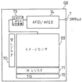
図14は、上述のような本発明の各実施例によるアナログFE(AFE1、AFE2)が搭載された固体撮像装置(CMOS型イメージセンサ)の全体構成例を示すブロック図である。
図中のアナログFE74が、上述したアナログFE1またはアナログFE2のいずれかによって構成されるブロックである。
この固体撮像装置は、半導体基板68上に、イメージセンサ領域69、垂直レジスタ70、水平レジスタ71、出力アンプ73、タイミングジェネレータTG72、アナログFE74の各ブロックを搭載したものであり、アナログFE74がイメージセンサと同一チップ上に形成された例である。
【0034】
このような固体撮像装置では、垂直ブランキング期間と水平ブランキング期間の少なくとも片方に黒基準信号を持っているが、実際の使用条件下においては、デバイス温度が時々刻々変動するため、上述したフィードバックループクランプ回路による黒基準電圧のクランプ動作により、イメージセンサ69の出力信号DRVoutの基準電圧を一定に維持することが可能となる。
したがって、本発明の固体撮像装置は、図示のようなCMOS型イメージセンサ用途に広く採用することができる。
また、CCDイメージセンサなどでは、上述した各実施例のアナログFEを別チップ構成で設けることができる。
すなわち、本発明は、CCDイメージセンサやCMOSイメージセンサに広く採用できるものである。
【0035】
以上のような本発明の各実施例による固体撮像装置およびクランプ制御方法では、以下のような効果を得ることが可能である。
1.フィードバックループのゲインを減少させたため、チップ内部、およびチップ外部から混入する雑音の影響を抑圧することができる。
2.各種雑音が混入しやすい外部端子のフローティング状態がなくなるため、ハム雑音などの影響を削減できる。
3.外部容量素子をチップ内部に作成することが可能となるため、このICを使用したシステムの小型化が可能である。
【0036】
【発明の効果】
以上説明したように本発明の固体撮像装置およびクランプ制御方法によれば、黒基準信号の期間に対応するゲインコントロールアンプの出力値を所定の基準値に一致させるクランプ回路に、ゲインコントロールアンプに供給されるクランプ信号のゲインを制御するゲイン制御手段を設けたことから、このクランプ回路に電源や外部回路等から各種の雑音が混入した場合にも、これをゲイン制御手段によって抑制し、ゲインコントロールアンプに対する影響を小さくすることが可能となり、撮像信号への雑音の影響を抑制することができる効果がある。
また、本発明の固体撮像装置によれば、フィールドバッククランプ期間以外の電圧変動を抑制するための第1の容量素子を接続するノードをクランプ期間以外でフローティング状態にならないようにしたことにより、クランプ期間以外の期間でクランプ回路の状態を安定化でき、ハム雑音等の影響を抑制することができる効果がある。
【図面の簡単な説明】
【図1】本発明の実施の形態で用いる動作原理を説明するための各信号の状態を示すタイミングチャートである。
【図2】本発明の第1実施例による固体撮像装置のアナログFEの構成を示すブロック図である。
【図3】図2に示す第1実施例の構成におけるゲイン制御手段の制御動作の具体例を示す説明図である。
【図4】本発明の第2実施例による固体撮像装置のアナログFEの構成を示すブロック図である。
【図5】本発明の第3実施例による固体撮像装置のアナログFEの構成を示すブロック図である。
【図6】本発明の第4実施例による固体撮像装置のアナログFEの構成を示すブロック図である。
【図7】本発明の第5実施例による固体撮像装置のアナログFEの構成を示すブロック図である。
【図8】本発明の第6実施例による固体撮像装置のアナログFEの構成を示すブロック図である。
【図9】本発明の第7実施例による固体撮像装置のアナログFEの構成を示すブロック図である。
【図10】本発明の第8実施例による固体撮像装置のアナログFEの構成を示すブロック図である。
【図11】本発明の第9実施例による固体撮像装置のアナログFEの構成を示すブロック図である。
【図12】本発明の第10実施例による固体撮像装置のアナログFEの構成を示すブロック図である。
【図13】本発明の第11実施例による固体撮像装置のアナログFEの構成を示すブロック図である。
【図14】本発明の各実施例によるアナログFEが搭載された固体撮像装置(CMOS型イメージセンサ)の全体構成例を示すブロック図である。
【図15】従来の固体撮像装置に設けられるアナログFEの第1の構成例を示すブロック図である。
【図16】従来の固体撮像装置に設けられるアナログFEの第2の構成例を示すブロック図である。
【図17】従来の固体撮像装置において電源に混入する雑音電圧の具体例を示す説明図である。
【符号の説明】
1、2……アナログFE、3……CDS回路、4……AGC回路、5……LPF回路、6……DRVアンプ、9、15……コンデンサ、11……基準電圧源、12……OPアンプ、18……クランプ回路、18A……フィードバックループ、18B……スイッチ、36……電圧電流変換回路。[0001]
BACKGROUND OF THE INVENTION
The present invention relates to a solid-state imaging device that uses an image signal captured by an image sensor as a control signal by feeding back the image signal, and a clamp control method thereof.
[0002]
[Prior art]
FIG. 15 is a block diagram illustrating an example of an analog front-end processor (hereinafter referred to as analog FE) provided in a conventional solid-state imaging device.
The
[0003]
The
A
The
The clamp control signal CLPOB is input from the
[0004]
An IC constituting such an analog FE1 is often used as a signal processing IC for an output signal of a solid-state imaging device such as a CCD image sensor or a CMOS image sensor.
Conventional CCD image sensors and CMOS image sensors generally have a black reference signal in at least one of a vertical blanking period and a horizontal blanking period, and during a black reference signal output period of one frame period or one horizontal period. Then, the clamp control signal CLPOB by the external input is turned “ON”, the
As a result, even if the black reference signal voltage of the input signal varies, the output signal DRVout can always be output based on the constant reference voltage value Vref.
[0005]
FIG. 16 is a block diagram showing an analog FE2 provided in a solid-state imaging device according to another conventional example. In FIG. 16, elements common to FIG. 15 are denoted by the same reference numerals.
16 includes the
Further, the
This type of analog FE is used not only for a CDS function and an AGC function but also for a one-chip circuit including an AD function and a TG function for driving an image sensor. Furthermore, it is also widely used for solid-state imaging devices such as CCDs and CMOS image sensors incorporated in these functional chips.
[0006]
[Problems to be solved by the invention]
However, in the conventional circuit configuration described above, it is difficult to prevent the influence of noise mixed in from the power supply voltage or GND.
FIG. 17 is an explanatory diagram showing a specific example of the noise voltage mixed in the power supply as described above, where the vertical axis indicates the noise voltage and the horizontal axis indicates the frequency.
The output signal DRVout from the above-described IC chip is delivered to the next-stage signal processing board (or signal processing IC), but there is a problem of noise mixing from this signal processing board (or signal processing IC).
As shown in the figure, the noise mixed in the image includes 30 Hz noise corresponding to the frame frequency mixed from the next-stage signal processing board (or signal processing IC), its harmonic frequency noise, and 50 Hz mixed from the power source. Noise and noise of the higher harmonic frequency.
Therefore, it is necessary to suppress the noise mixed from such a power supply and the noise mixed from the next-stage signal processing board (or signal processing IC).
[0007]
Furthermore, in order to prevent the fluctuation of the external terminal voltage other than the feedback period, it is necessary to draw at least one
This capacitance value is as large as about 0.1 μF to 10 μF, requires a large component volume, and it has been difficult to miniaturize a camera system using an IC chip as described above.
[0008]
The present invention has been made in view of such a situation, and an object thereof is to clamp an output signal in a black reference signal period in an analog front-end IC chip provided with a CDS function, an AGC function, or the like. An object of the present invention is to provide a solid-state imaging device capable of suppressing the influence of noise mixed in a clamp circuit from a power source, an external circuit, and the like, and capable of simplifying an IC chip, and a clamp control method thereof. .
[0009]
[Means for Solving the Problems]
The present invention provides an image sensor having a black reference signal in at least one of a vertical blanking period and a horizontal blanking period, a correlated double sampling circuit for removing noise from an output signal from the image sensor, and the correlated double In the solid-state imaging device, comprising: a gain control amplifier that amplifies an output signal of the sampling circuit; and a clamp circuit that matches an output value of the gain control amplifier corresponding to a period of the black reference signal with a predetermined reference value. The circuit includes a feedback loop for feedback control of the gain control amplifier based on an output signal, an arithmetic means for outputting a clamp signal by comparing the output signal fed back by the feedback loop with the reference value, and the black reference Corresponding to the duration of the signal And a switch for opening and closing the serial feedback loop further gain of the clamp signal supplied to the gain control amplifier To make it smaller Gain control means for controlling is provided.
[0010]
The present invention also provides an image sensor having a black reference signal in at least one of a vertical blanking period and a horizontal blanking period, a correlated double sampling circuit for removing noise from an output signal from the image sensor, and the correlated two-sample circuit. A solid-state imaging device comprising: a gain control amplifier that amplifies an output signal of a multiple sampling circuit; and a clamp circuit that matches an output value of the gain control amplifier corresponding to a period of the black reference signal with a predetermined reference value. The clamp circuit includes a feedback loop for feedback control of the gain control amplifier based on an output signal, an arithmetic means for comparing the output signal fed back by the feedback loop with the reference value, and outputting a clamp signal, and the black circuit Corresponds to the period of the reference signal And a switch for opening and closing the feedback loop Te, further, other than the field back clamp period Of the clamp signal supplied to the gain control amplifier. At least one node connecting the first capacitive element for suppressing voltage fluctuations; Provided on the output side of the computing means, and provided the switch on the feedback input side of the computing means, The node is configured not to be in a floating state except for a clamp period.
[0011]
The present invention also provides an image sensor having a black reference signal in at least one of a vertical blanking period and a horizontal blanking period, a correlated double sampling circuit for removing noise from an output signal from the image sensor, and the correlated two-sample circuit. A gain control amplifier that amplifies the output signal of the multiple sampling circuit; and a clamp circuit that matches an output value of the gain control amplifier corresponding to a period of the black reference signal with a predetermined reference value. A feedback loop for feedback-controlling the gain control amplifier based on the output signal, an arithmetic means for outputting a clamp signal by comparing the output signal fed back by the feedback loop with the reference value, and a period of the black reference signal In response to said feedback A clamp control method of a solid-state imaging device having a switch for opening and closing the-loop, by another of the gain control means and said calculating means a gain of the clamp signal supplied to the gain control amplifier To make it smaller It is characterized by being controlled.
[0012]
According to the solid-state imaging device and the clamp control method of the present invention, the clamp signal supplied to the gain control amplifier is supplied to the clamp circuit that matches the output value of the gain control amplifier corresponding to the period of the black reference signal with a predetermined reference value. Since the gain control means for controlling the gain is provided, even if various noises are mixed into the clamp circuit from the power supply, external circuit, etc., this is suppressed by the gain control means and the influence on the gain control amplifier is reduced. Thus, the influence of noise on the imaging signal can be suppressed.
Further, according to the solid-state imaging device of the present invention, the node connecting the first capacitive element for suppressing voltage fluctuations other than the feedback clamp period is prevented from being in a floating state other than the clamp period, so that the clamp period It is possible to stabilize the state of the clamp circuit during a period other than the above, and to suppress the influence of hum noise or the like.
[0013]
DETAILED DESCRIPTION OF THE INVENTION
Next, embodiments of the present invention will be described with reference to the drawings.
FIG. 1 is a timing chart showing the state of each signal for explaining the operating principle used in the embodiment of the present invention.
This timing chart shows a horizontal timing period (H timing) 30, an analog FE output signal (DRVout) 31, and a clamp control signal (CLPOB) for causing the analog FE to perform a clamping operation in the solid-state imaging device according to the present embodiment. ) 32, an
[0014]
Here, the
In this example, a clamping operation is performed by the first CLPOB signal 32-1 for a part of the area of the signal 31-1 in the previous black reference period.
That is, the feedback loop circuit of the analog FE is operated only in the CLPOB period 32-1, and the output of the
By such a feedback operation, even if the voltage level of the previous OPB period 31-1 of the
That is, the reference signal voltage 31-1 of the output voltage DRVout is always set to a constant voltage output value Vref regardless of temperature fluctuations.
In this way, the influence of the temperature change can be eliminated by performing the feedback operation of the output voltage DRVout31-1 in the first CLPOB period 32-1.
[0015]
In this example, as a countermeasure against noise, by providing a current-voltage conversion circuit for adjusting the gain of the feedback loop 33-1 to a predetermined magnitude during the feedback clamp period as described above, the power supply and GND are used during feedback. This suppresses the noise generated by the noise (noise countermeasure 34-1A).
Further, in a configuration in which a large-capacity external capacitor (first capacitive element) is connected outside the IC in the period 33-2 other than the feedback clamp period, a path in which external noise is not mixed from the external connection terminal to which the external capacitor is connected. (Noise countermeasure 34-1B).
[0016]
Hereinafter, specific examples for realizing the features of the present embodiment as described above will be sequentially invented. In each of the following embodiments, the same reference numerals are used to describe the same configuration as that of the conventional example described above.
FIG. 2 is a block diagram showing the configuration of the analog FE of the solid-state imaging device according to the first embodiment of the present invention.
This analog FE1 is obtained by adding a voltage-current conversion circuit (attenuation amplifier) 36 to the above-described conventional example of FIG. 15, and the
[0017]
Similarly to the example shown in FIG. 15, the
The
[0018]
Here, since the
However, for example, noise mixed from the power supply or GND of the
Therefore, in order to suppress the influence of this noise, a circuit for controlling the feedback loop gain is indispensable inside the
Therefore, in this example, a voltage /
Here, the output of the voltage-
[0019]
In this example, the voltage /
In short, in addition to the
[0020]
FIG. 3 is an explanatory diagram showing a specific example of the control operation of the gain control means in the configuration of the first embodiment shown in FIG. 2 described above, with respect to the change (horizontal axis) of the output signal DRVout that is the input of the
As shown by the solid line C in the figure, when the gain of the feedback loop is large, the voltage fluctuation ΔVout fed back with respect to the small fluctuation of the output voltage DRVout also becomes large, and the noise of the power source such as the
Therefore, as indicated by a broken line D in the figure, it is possible to improve the characteristic against noise fluctuation by setting the feedback loop gain to a predetermined value or less by inserting the voltage-
That is, by setting ΔVfb <ΔVout, it is possible to suppress the influence of noise mixed in from the power source and the GND of the
[0021]
FIG. 4 is a block diagram showing the configuration of the analog FE of the solid-state imaging device according to the second embodiment of the present invention.
Basically, the configuration is the same as that shown in FIG. 2, but in this example, a
That is, in this example, the
The rest is the same as the example shown in FIG.
[0022]
FIG. 5 is a block diagram showing the configuration of the analog FE of the solid-state imaging device according to the third embodiment of the present invention.
In this example, a
With such a circuit configuration, it is not necessary to provide an external connection terminal, and the following effects can be obtained.
First, if an external connection terminal is pulled out, noise cannot be avoided from the external terminal.
Second, if a capacitor with a large capacitance value of about 0.1 μF to 10 μF is attached to the external terminal, the volume of the capacitor increases, making it difficult to reduce the size of the entire system. Thus, it is possible to reduce the size.
The rest is the same as the example shown in FIG.
[0023]
FIG. 6 is a block diagram showing the configuration of the analog FE of the solid-state imaging device according to the fourth embodiment of the present invention.
In this example, switches 44 and 45 for switching the input of the
That is, in this example, the
[0024]
Then, the
Further, by switching the
Further, by switching the
[0025]
The configuration of this example is intended for the noise countermeasure 34-2B of FIG. That is, conventionally, the
That is, in the configuration of FIG. 6, the
Further, when the clamp period ends, the
As a result, the voltage written in the
In this way, it is possible to obtain a configuration in which the
In the example of FIG. 6, the
That is, it can be reduced. Similarly, the
[0026]
FIG. 7 is a block diagram showing the configuration of the analog FE of the solid-state imaging device according to the fifth embodiment of the present invention.
The analog FE1 of this example is provided with a minute
By generating the minute voltage ΔVref by the minute
[0027]
FIG. 8 is a block diagram showing the configuration of the analog FE of the solid-state imaging device according to the sixth embodiment of the present invention.
This embodiment is a modification of the second embodiment shown in FIG. 4, and is similar to the third embodiment of FIG. 5 in place of the
Note that the
[0028]
FIG. 9 is a block diagram showing the configuration of the analog FE of the solid-state imaging device according to the seventh embodiment of the present invention.
In this example, the other electrode of the
This is due to the common GND (or common VDD) on the external board, causing the effects of noise mixed in from the external terminals to occur simultaneously on the two capacitors, increasing the common-mode input noise rejection ratio, and suppressing the effects of noise. To do.
[0029]
FIG. 10 is a block diagram showing the configuration of the analog FE of the solid-state imaging device according to the eighth embodiment of the present invention.
In this example, the present invention is applied to the analog FE2 having the configuration shown in FIG. 16, and an
[0030]
FIG. 11 is a block diagram showing the configuration of the analog FE of the solid-state imaging device according to the ninth embodiment of the present invention.
In this example, in the configuration shown in FIG. 10, a
With such a circuit configuration, it is possible to control a large gain of the
[0031]
FIG. 12 is a block diagram showing the configuration of the analog FE of the solid-state imaging device according to the tenth embodiment of the present invention.
In this example, in the
That is, in FIG. 12, the
In such a configuration, the output signal of the low-
Therefore, even if the
[0032]
FIG. 13 is a block diagram showing the configuration of the analog FE of the solid-state imaging device according to the eleventh embodiment of the present invention.
In this example, the principle shown in FIG. 6 is applied to the
The
The
In such a configuration, the
Thereby, the voltage written in the
[0033]
FIG. 14 is a block diagram showing an example of the overall configuration of a solid-state imaging device (CMOS type image sensor) on which analog FEs (AFE1, AFE2) according to the embodiments of the present invention as described above are mounted.
An
This solid-state image pickup device includes an
[0034]
Such a solid-state imaging device has a black reference signal in at least one of a vertical blanking period and a horizontal blanking period. However, under actual use conditions, the device temperature fluctuates from moment to moment. The reference voltage of the output signal DRVout of the
Therefore, the solid-state imaging device of the present invention can be widely used for CMOS image sensor applications as shown.
In a CCD image sensor or the like, the analog FE of each of the above embodiments can be provided in a separate chip configuration.
That is, the present invention can be widely applied to CCD image sensors and CMOS image sensors.
[0035]
In the solid-state imaging device and the clamp control method according to each embodiment of the present invention as described above, the following effects can be obtained.
1. Since the gain of the feedback loop is reduced, it is possible to suppress the influence of noise mixed from inside the chip and from outside the chip.
2. Since there is no floating state of external terminals that are likely to contain various types of noise, the effects of hum noise can be reduced.
3. Since it is possible to create the external capacitance element inside the chip, it is possible to reduce the size of a system using this IC.
[0036]
【The invention's effect】
As described above, according to the solid-state imaging device and the clamp control method of the present invention, the gain control amplifier is supplied to the clamp circuit that matches the output value of the gain control amplifier corresponding to the period of the black reference signal to the predetermined reference value. Gain control means that controls the gain of the clamp signal to be controlled, so that even if various noises are mixed into the clamp circuit from the power supply or external circuit, this is controlled by the gain control means, and the gain control amplifier The effect on noise can be reduced, and the effect of noise on the imaging signal can be suppressed.
In addition, according to the solid-state imaging device of the present invention, the node connecting the first capacitive element for suppressing voltage fluctuations other than the field back clamp period is prevented from being in a floating state other than the clamp period. It is possible to stabilize the state of the clamp circuit in a period other than the period, and to suppress the influence of hum noise and the like.
[Brief description of the drawings]
FIG. 1 is a timing chart showing the state of each signal for explaining an operation principle used in an embodiment of the present invention.
FIG. 2 is a block diagram showing a configuration of an analog FE of the solid-state imaging device according to the first embodiment of the present invention.
FIG. 3 is an explanatory diagram showing a specific example of the control operation of the gain control means in the configuration of the first embodiment shown in FIG. 2;
FIG. 4 is a block diagram showing a configuration of an analog FE of a solid-state imaging device according to a second embodiment of the present invention.
FIG. 5 is a block diagram showing a configuration of an analog FE of a solid-state imaging device according to a third embodiment of the present invention.
FIG. 6 is a block diagram showing a configuration of an analog FE of a solid-state imaging device according to a fourth embodiment of the present invention.
FIG. 7 is a block diagram showing a configuration of an analog FE of a solid-state imaging device according to a fifth embodiment of the present invention.
FIG. 8 is a block diagram showing a configuration of an analog FE of a solid-state imaging device according to a sixth embodiment of the present invention.
FIG. 9 is a block diagram showing a configuration of an analog FE of a solid-state imaging device according to a seventh embodiment of the present invention.
FIG. 10 is a block diagram showing a configuration of an analog FE of a solid-state imaging device according to an eighth embodiment of the present invention.
FIG. 11 is a block diagram showing a configuration of an analog FE of a solid-state imaging device according to a ninth embodiment of the present invention.
FIG. 12 is a block diagram showing a configuration of an analog FE of a solid-state imaging device according to a tenth embodiment of the present invention.
FIG. 13 is a block diagram showing a configuration of an analog FE of a solid-state imaging device according to an eleventh embodiment of the present invention.
FIG. 14 is a block diagram showing an example of the overall configuration of a solid-state imaging device (CMOS image sensor) equipped with an analog FE according to each embodiment of the present invention.
FIG. 15 is a block diagram illustrating a first configuration example of an analog FE provided in a conventional solid-state imaging device.
FIG. 16 is a block diagram illustrating a second configuration example of an analog FE provided in a conventional solid-state imaging device.
FIG. 17 is an explanatory diagram illustrating a specific example of a noise voltage mixed in a power supply in a conventional solid-state imaging device.
[Explanation of symbols]
1, 2 ... Analog FE, 3 ... CDS circuit, 4 ... AGC circuit, 5 ... LPF circuit, 6 ... DRV amplifier, 9, 15 ... Capacitor, 11 ... Reference voltage source, 12 ...
Claims (10)
前記イメージセンサからの出力信号に対するノイズ除去を行う相関二重サンプリング回路と、
前記相関二重サンプリング回路の出力信号を増幅するゲインコントロールアンプと、
前記黒基準信号の期間に対応する前記ゲインコントロールアンプの出力値を所定の基準値に一致させるクランプ回路とを具備した固体撮像装置において、
前記クランプ回路は、ゲインコントロールアンプを出力信号に基づいてフィードバック制御するためのフィードバックループと、前記フィードバックループによってフィードバックされた出力信号を前記基準値と比較してクランプ信号を出力する演算手段と、前記黒基準信号の期間に対応して前記フィードバックループを開閉するスイッチとを有し、
さらに、前記ゲインコントロールアンプに供給されるクランプ信号のゲインを小さくするように制御するゲイン制御手段を有する、
ことを特徴とする固体撮像装置。An image sensor having a black reference signal in at least one of a vertical blanking period and a horizontal blanking period;
A correlated double sampling circuit for removing noise with respect to an output signal from the image sensor;
A gain control amplifier that amplifies the output signal of the correlated double sampling circuit;
In a solid-state imaging device comprising a clamp circuit that matches an output value of the gain control amplifier corresponding to a period of the black reference signal with a predetermined reference value,
The clamp circuit includes a feedback loop for feedback-controlling a gain control amplifier based on an output signal, an arithmetic unit for comparing the output signal fed back by the feedback loop with the reference value, and outputting a clamp signal, A switch for opening and closing the feedback loop corresponding to the period of the black reference signal,
Furthermore, it has a gain control means for controlling to reduce the gain of the clamp signal supplied to the gain control amplifier,
A solid-state imaging device.
前記イメージセンサからの出力信号に対するノイズ除去を行う相関二重サンプリング回路と、
前記相関二重サンプリング回路の出力信号を増幅するゲインコントロールアンプと、
前記黒基準信号の期間に対応する前記ゲインコントロールアンプの出力値を所定の基準値に一致させるクランプ回路とを具備した固体撮像装置において、
前記クランプ回路は、ゲインコントロールアンプを出力信号に基づいてフィードバック制御するためのフィードバックループと、前記フィードバックループによってフィードバックされた出力信号を前記基準値と比較してクランプ信号を出力する演算手段と、前記黒基準信号の期間に対応して前記フィードバックループを開閉するスイッチとを有し、
さらに、フィールドバッククランプ期間以外で前記ゲインコントロールアンプに供給されるクランプ信号の電圧変動を抑制するための第1の容量素子を接続する少なくとも1つのノードを前記演算手段の出力側に設け、かつ、前記スイッチを前記演算手段のフィードバック入力側に設け、前記ノードがクランプ期間以外でフローティング状態にならないようにした、
ことを特徴とする固体撮像装置。An image sensor having a black reference signal in at least one of a vertical blanking period and a horizontal blanking period;
A correlated double sampling circuit for removing noise with respect to an output signal from the image sensor;
A gain control amplifier that amplifies the output signal of the correlated double sampling circuit;
In a solid-state imaging device comprising a clamp circuit that matches an output value of the gain control amplifier corresponding to a period of the black reference signal with a predetermined reference value,
The clamp circuit includes a feedback loop for feedback-controlling a gain control amplifier based on an output signal, an arithmetic unit for comparing the output signal fed back by the feedback loop with the reference value, and outputting a clamp signal, A switch for opening and closing the feedback loop corresponding to the period of the black reference signal,
Furthermore, at least one node for connecting the first capacitive element for suppressing voltage fluctuation of the clamp signal supplied to the gain control amplifier outside the field back clamp period is provided on the output side of the arithmetic means, and The switch is provided on the feedback input side of the arithmetic means so that the node does not enter a floating state other than the clamp period.
A solid-state imaging device.
前記イメージセンサからの出力信号に対するノイズ除去を行う相関二重サンプリング回路と、
前記相関二重サンプリング回路の出力信号を増幅するゲインコントロールアンプと、
前記黒基準信号の期間に対応する前記ゲインコントロールアンプの出力値を所定の基準値に一致させるクランプ回路とを具備し、
前記クランプ回路は、ゲインコントロールアンプを出力信号に基づいてフィードバック制御するためのフィードバックループと、前記フィードバックループによってフィードバックされた出力信号を前記基準値と比較してクランプ信号を出力する演算手段と、前記黒基準信号の期間に対応して前記フィードバックループを開閉するスイッチとを有する固体撮像装置のクランプ制御方法であって、
前記ゲインコントロールアンプに供給されるクランプ信号のゲインを前記演算手段とは別のゲイン制御手段によって小さくするように制御するようにした、
ことを特徴とする固体撮像装置のクランプ制御方法。An image sensor having a black reference signal in at least one of a vertical blanking period and a horizontal blanking period;
A correlated double sampling circuit for removing noise with respect to an output signal from the image sensor;
A gain control amplifier that amplifies the output signal of the correlated double sampling circuit;
A clamp circuit that matches an output value of the gain control amplifier corresponding to a period of the black reference signal with a predetermined reference value;
The clamp circuit includes a feedback loop for feedback-controlling a gain control amplifier based on an output signal, an arithmetic unit for comparing the output signal fed back by the feedback loop with the reference value, and outputting a clamp signal, A clamp control method for a solid-state imaging device having a switch for opening and closing the feedback loop corresponding to a period of a black reference signal,
The gain of the clamp signal supplied to the gain control amplifier is controlled to be reduced by a gain control means different from the calculation means.
A clamp control method for a solid-state imaging device.
Priority Applications (5)
| Application Number | Priority Date | Filing Date | Title |
|---|---|---|---|
| JP2001358892A JP3831940B2 (en) | 2001-11-26 | 2001-11-26 | Solid-state imaging device and clamp control method thereof |
| US10/292,085 US7463282B2 (en) | 2001-11-26 | 2002-11-12 | Solid-state image pickup device and clamp control method therefor |
| CN02156964.9A CN1255993C (en) | 2001-11-26 | 2002-11-26 | Solid image pick-up device and its pinch position control method |
| CN200410100324.9A CN1620106A (en) | 2001-11-26 | 2002-11-26 | Solid image pick-up device and its pinch position control method |
| US12/264,030 US20090066823A1 (en) | 2001-11-26 | 2008-11-03 | Solid-state image pickup device and clamp control method therefor |
Applications Claiming Priority (1)
| Application Number | Priority Date | Filing Date | Title |
|---|---|---|---|
| JP2001358892A JP3831940B2 (en) | 2001-11-26 | 2001-11-26 | Solid-state imaging device and clamp control method thereof |
Publications (2)
| Publication Number | Publication Date |
|---|---|
| JP2003163845A JP2003163845A (en) | 2003-06-06 |
| JP3831940B2 true JP3831940B2 (en) | 2006-10-11 |
Family
ID=19169996
Family Applications (1)
| Application Number | Title | Priority Date | Filing Date |
|---|---|---|---|
| JP2001358892A Expired - Fee Related JP3831940B2 (en) | 2001-11-26 | 2001-11-26 | Solid-state imaging device and clamp control method thereof |
Country Status (3)
| Country | Link |
|---|---|
| US (2) | US7463282B2 (en) |
| JP (1) | JP3831940B2 (en) |
| CN (2) | CN1255993C (en) |
Families Citing this family (24)
| Publication number | Priority date | Publication date | Assignee | Title |
|---|---|---|---|---|
| US6988667B2 (en) | 2001-05-31 | 2006-01-24 | Alien Technology Corporation | Methods and apparatuses to identify devices |
| US7193504B2 (en) | 2001-10-09 | 2007-03-20 | Alien Technology Corporation | Methods and apparatuses for identification |
| US7417675B2 (en) * | 2003-05-12 | 2008-08-26 | Altasens, Inc. | On-chip black clamp system and method |
| JP2005045558A (en) * | 2003-07-22 | 2005-02-17 | Sony Corp | Image pickup apparatus |
| US8102244B2 (en) | 2003-08-09 | 2012-01-24 | Alien Technology Corporation | Methods and apparatuses to identify devices |
| JP4345403B2 (en) | 2003-08-21 | 2009-10-14 | セイコーエプソン株式会社 | Image reading device |
| US7716160B2 (en) | 2003-11-07 | 2010-05-11 | Alien Technology Corporation | Methods and apparatuses to identify devices |
| US7626622B2 (en) | 2004-01-13 | 2009-12-01 | Panasonic Corporation | Solid state image pickup device and camera using the same |
| US7750955B2 (en) * | 2004-08-31 | 2010-07-06 | Canon Kabushiki Kaisha | Image signal processing apparatus, image signal processing method and camera using the image signal processing apparatus |
| JP4723592B2 (en) * | 2004-11-01 | 2011-07-13 | アルタセンス、インコーポレイテッド | On-chip black clamp system and method |
| JP4760100B2 (en) * | 2005-04-06 | 2011-08-31 | トヨタ自動車株式会社 | Image processing apparatus and vehicle driving support apparatus using the same |
| KR100719370B1 (en) | 2005-08-03 | 2007-05-17 | 삼성전자주식회사 | Analog-to-digital converter and cmos image sensor with the same and method of operating cmos image sensor |
| US7715165B2 (en) * | 2006-07-11 | 2010-05-11 | Silicon Laboratories, Inc. | System and method of surge protection in a powered device |
| JP5123601B2 (en) * | 2006-08-31 | 2013-01-23 | キヤノン株式会社 | Photoelectric conversion device |
| WO2008069228A1 (en) * | 2006-12-08 | 2008-06-12 | Panasonic Corporation | Video signal output circuit and semiconductor integrated circuit having same |
| US7495479B1 (en) * | 2007-09-13 | 2009-02-24 | Faraday Technology Corp. | Sample and hold circuit and related data signal detecting method utilizing sample and hold circuit |
| JP2009159205A (en) * | 2007-12-26 | 2009-07-16 | Panasonic Corp | Imaging device and semiconductor integrated circuit |
| JP5188221B2 (en) * | 2008-03-14 | 2013-04-24 | キヤノン株式会社 | Solid-state imaging device |
| US8035073B2 (en) * | 2008-11-25 | 2011-10-11 | Analog Devices, Inc. | Switched capacitor input stage for imaging front-ends |
| JP5114448B2 (en) * | 2009-03-27 | 2013-01-09 | 富士フイルム株式会社 | Solid-state imaging device, driving method of solid-state imaging device, and imaging apparatus |
| JP5063714B2 (en) * | 2010-01-29 | 2012-10-31 | シャープ株式会社 | Image reading apparatus and image forming apparatus |
| US9083889B2 (en) * | 2010-02-28 | 2015-07-14 | Himax Imaging, Inc. | Signal processing circuit capable of selectively adjusting gain factor of sample-and-hold circuit and signal processing method thereof |
| JP5545471B2 (en) * | 2010-03-26 | 2014-07-09 | 株式会社リコー | Image reading apparatus, image reading method, and program |
| CN104092964B (en) * | 2014-07-30 | 2018-02-16 | 昆山锐芯微电子有限公司 | Correlated double sampling circuit and control method, image sensor system and control method |
Family Cites Families (7)
| Publication number | Priority date | Publication date | Assignee | Title |
|---|---|---|---|---|
| US5121230A (en) * | 1987-01-19 | 1992-06-09 | Canon Kabushiki Kaisha | Image reading apparatus having adjusting circuits for matching the level of and compensating for fluctuation among a plurality of sensing elements |
| US6456326B2 (en) * | 1994-01-28 | 2002-09-24 | California Institute Of Technology | Single chip camera device having double sampling operation |
| JP3971102B2 (en) * | 1997-11-04 | 2007-09-05 | 株式会社ルネサステクノロジ | Image input system |
| KR100284284B1 (en) * | 1998-11-05 | 2001-03-02 | 김영환 | Analog signal processing device of digital camera |
| US6750910B1 (en) * | 1998-07-15 | 2004-06-15 | Texas Instruments Incorporated | Optical black and offset correction in CCD signal processing |
| JP4384747B2 (en) * | 1998-08-24 | 2009-12-16 | マグナチップセミコンダクター有限会社 | Black level adjustment device for video camera |
| US6587143B1 (en) * | 1999-01-19 | 2003-07-01 | National Semiconductor Corporation | Correlated double sampler with single amplifier |
-
2001
- 2001-11-26 JP JP2001358892A patent/JP3831940B2/en not_active Expired - Fee Related
-
2002
- 2002-11-12 US US10/292,085 patent/US7463282B2/en not_active Expired - Fee Related
- 2002-11-26 CN CN02156964.9A patent/CN1255993C/en not_active Expired - Fee Related
- 2002-11-26 CN CN200410100324.9A patent/CN1620106A/en active Pending
-
2008
- 2008-11-03 US US12/264,030 patent/US20090066823A1/en not_active Abandoned
Also Published As
| Publication number | Publication date |
|---|---|
| US20030117676A1 (en) | 2003-06-26 |
| US7463282B2 (en) | 2008-12-09 |
| CN1422081A (en) | 2003-06-04 |
| JP2003163845A (en) | 2003-06-06 |
| CN1620106A (en) | 2005-05-25 |
| CN1255993C (en) | 2006-05-10 |
| US20090066823A1 (en) | 2009-03-12 |
Similar Documents
| Publication | Publication Date | Title |
|---|---|---|
| JP3831940B2 (en) | Solid-state imaging device and clamp control method thereof | |
| US7208983B2 (en) | Image-sensor signal processing circuit | |
| US6940548B2 (en) | Analog optical black clamping circuit for a charge coupled device having wide programmable gain range | |
| US5736886A (en) | Input clamping method and apparatus with a correlated double-sampling circuit | |
| US8243190B2 (en) | Solid state image pickup device and camera with focus detection using level shifting | |
| EP2448254B1 (en) | Solid-state image pickup device | |
| EP2433421A1 (en) | Image capturing device, image capturing system, and method of driving image capturing device | |
| JP7353783B2 (en) | Imaging device and its control method; Imaging device and its control method | |
| JPH09326698A (en) | Offset correction method and device | |
| EP2360912A1 (en) | Solid-state image pickup apparatus and driving method therefor | |
| US6801254B1 (en) | Image pickup device in which the charge coupled device and correlated double sampling circuitry are on a chip separate from the gain control amplifier circuitry and analog-to-digital converter circuitry | |
| JP3075203B2 (en) | Solid-state imaging device | |
| US6441686B1 (en) | Offset correction method and apparatus | |
| JP3751187B2 (en) | Solid-state imaging device | |
| JP2006270419A (en) | Buffer amplifier for single power source, reference voltage supply circuit, and imaging apparatus | |
| JPH10164442A (en) | Correlated double sampling circuit | |
| JP2000350194A (en) | Electronic endoscope system | |
| US8134602B2 (en) | Amplifier circuit | |
| JP2007312065A (en) | Clamp circuit and video signal processor using same | |
| JP3287483B2 (en) | Sample hold circuit and output circuit | |
| KR200333736Y1 (en) | Aperture drive circuit with backlight compensation function | |
| JP2006191211A (en) | Clamp circuit | |
| KR200141208Y1 (en) | Contour signal generating circuit for camcorder | |
| JPH0965222A (en) | Head amplifier driver for solid-state image pickup device | |
| JPS6316776A (en) | Direct current restoration circuit |
Legal Events
| Date | Code | Title | Description |
|---|---|---|---|
| A131 | Notification of reasons for refusal |
Free format text: JAPANESE INTERMEDIATE CODE: A131 Effective date: 20051222 |
|
| A521 | Request for written amendment filed |
Free format text: JAPANESE INTERMEDIATE CODE: A523 Effective date: 20060217 |
|
| TRDD | Decision of grant or rejection written | ||
| A01 | Written decision to grant a patent or to grant a registration (utility model) |
Free format text: JAPANESE INTERMEDIATE CODE: A01 Effective date: 20060626 |
|
| A61 | First payment of annual fees (during grant procedure) |
Free format text: JAPANESE INTERMEDIATE CODE: A61 Effective date: 20060709 |
|
| LAPS | Cancellation because of no payment of annual fees |