JP3831592B2 - Method for producing compound semiconductor thin film - Google Patents
Method for producing compound semiconductor thin film Download PDFInfo
- Publication number
- JP3831592B2 JP3831592B2 JP2000270033A JP2000270033A JP3831592B2 JP 3831592 B2 JP3831592 B2 JP 3831592B2 JP 2000270033 A JP2000270033 A JP 2000270033A JP 2000270033 A JP2000270033 A JP 2000270033A JP 3831592 B2 JP3831592 B2 JP 3831592B2
- Authority
- JP
- Japan
- Prior art keywords
- group
- thin film
- layer
- substrate
- sputtering
- Prior art date
- Legal status (The legal status is an assumption and is not a legal conclusion. Google has not performed a legal analysis and makes no representation as to the accuracy of the status listed.)
- Expired - Fee Related
Links
Images


Classifications
-
- Y—GENERAL TAGGING OF NEW TECHNOLOGICAL DEVELOPMENTS; GENERAL TAGGING OF CROSS-SECTIONAL TECHNOLOGIES SPANNING OVER SEVERAL SECTIONS OF THE IPC; TECHNICAL SUBJECTS COVERED BY FORMER USPC CROSS-REFERENCE ART COLLECTIONS [XRACs] AND DIGESTS
- Y02—TECHNOLOGIES OR APPLICATIONS FOR MITIGATION OR ADAPTATION AGAINST CLIMATE CHANGE
- Y02E—REDUCTION OF GREENHOUSE GAS [GHG] EMISSIONS, RELATED TO ENERGY GENERATION, TRANSMISSION OR DISTRIBUTION
- Y02E10/00—Energy generation through renewable energy sources
- Y02E10/50—Photovoltaic [PV] energy
- Y02E10/541—CuInSe2 material PV cells
-
- Y—GENERAL TAGGING OF NEW TECHNOLOGICAL DEVELOPMENTS; GENERAL TAGGING OF CROSS-SECTIONAL TECHNOLOGIES SPANNING OVER SEVERAL SECTIONS OF THE IPC; TECHNICAL SUBJECTS COVERED BY FORMER USPC CROSS-REFERENCE ART COLLECTIONS [XRACs] AND DIGESTS
- Y02—TECHNOLOGIES OR APPLICATIONS FOR MITIGATION OR ADAPTATION AGAINST CLIMATE CHANGE
- Y02P—CLIMATE CHANGE MITIGATION TECHNOLOGIES IN THE PRODUCTION OR PROCESSING OF GOODS
- Y02P70/00—Climate change mitigation technologies in the production process for final industrial or consumer products
- Y02P70/50—Manufacturing or production processes characterised by the final manufactured product
Landscapes
- Physical Deposition Of Substances That Are Components Of Semiconductor Devices (AREA)
- Photovoltaic Devices (AREA)
- Physical Vapour Deposition (AREA)
Description
【0001】
【発明の属する技術分野】
本発明は、化合物半導体薄膜の製造方法および装置ならびにこれから得られる化合物半導体薄膜に関する。より詳細には、本発明は、薄膜太陽電池の分野において利用されるIB族元素、IIIB族元素およびVIB族元素を含む化合物半導体薄膜の製造方法および装置ならびにこれから得られる化合物半導体薄膜に関する。
【0002】
【従来の技術】
近年、薄膜太陽電池を構成する光吸収層として、IB族元素、IIIB族元素およびVIB族元素からなるカルコパイライト構造を有する化合物半導体薄膜が使用されている。このような化合物半導体薄膜としては、例えば、CuInSe2膜(いわゆる「CIS」膜)、CuInGaSe2膜(詳細にはCu(In、Ga)Se2膜、いわゆる「CIGS」膜)などが挙げられる。
【0003】
このような化合物半導体薄膜の従来の製造方法は、一般的に、蒸着法を用いる方法とスパッタリング法を用いる方法とに大別される。以下、これらの方法の例として、CuInSe2膜を形成する場合の代表的な方法についていくつか説明する。
【0004】
蒸着法を用いる従来の方法としては、目的の化合物半導体薄膜の構成元素を蒸着法により高温の基板上に多段階で供給する方法が挙げられる。この方法においては、Cu蒸発原料、In蒸発原料、Se蒸発原料がそれぞれ設置された蒸着源を備え、所定の圧力に保持された真空チャンバ内で、例えば上面にMo膜を備えるガラス基板を室温よりも高い約325℃の温度に加熱した状態で、まず第1段階として、In蒸発原料およびSe蒸発原料を加熱して蒸発させ、基板上にInおよびSeを供給して、比較的低温の基板上にIn−Se層を形成する。次に第2段階として、基板を更に加熱して約500〜600℃の高温とし、この状態で、Cu蒸発原料およびSe蒸発原料を加熱して蒸発させ、CuおよびSeをそれぞれ蒸着法により供給する。このとき、基板が高温状態にあるので、In−Se層表面に供給されたCuおよびSeは、In−Se層の上に積層されずにIn−Se層中に取り込まれて化合物を形成し、これにより、Cu−In−Se化合物層が成長する。最後に第3段階として、基板を高温に保った状態で、In蒸発原料およびSe蒸発原料を加熱して蒸発させ、InおよびSeをそれぞれ蒸着法により供給する。この段階においても、Cu−In−Se層表面に供給されたCuおよびSeは、この層の中に取り込まれて化合物を形成して、Cu−In−Se化合物層が成長し、最終的にCuInSe2膜を形成する。
【0005】
他方、スパッタリング法を用いる従来の方法としては、目的の化合物半導体薄膜の構成元素をスパッタリング法により基板上に一段階で供給する方法が挙げられる。この方法においては、例えばCuターゲット、Inターゲット、およびSeターゲットがそれぞれ設置されたスパッタ源を備え、所定の圧力に保持された真空チャンバ内で、各ターゲットをスパッタリングして、上述のような基板上にCu、In、およびSeを同時に供給し、これによりCuInSe2膜が成長して形成される。ターゲットとしては、Cu、In、およびSeからなる群から選択される任意の組み合わせの材料からなるターゲットを用いることもできる。
【0006】
また、スパッタリング法を用いるもう1つの従来の方法として、目的の化合物半導体薄膜のSe以外の構成元素をスパッタリング法により基板上に多段階で供給して積層膜を形成し、その後、セレン化水素(H2Se)雰囲気で基板を熱処理する方法がある。この方法においては、まず、所定の圧力に保持された真空チャンバ内で、上述のような基板上に例えばCuターゲットをスパッタリングしてCuを供給し、次いでInターゲットをスパッタリングしてInを供給し、これによりCu膜およびIn膜を順次形成して積層膜とする。次いで、得られた基板をセレン化水素雰囲気で約500℃に加熱して熱処理(またはSe化処理とも言う)する。このときCu膜およびIn膜からなる積層膜はSeを取り込んで、化合物形成しながら成長して、最終的にCuInSe2膜を形成する。
【0007】
上述のような方法に加えて、目的の化合物半導体薄膜のSe以外の構成元素をスパッタリング法により、同時にSeを蒸着法により一段階で基板上に供給する方法がある。この方法においては、所定の圧力に保持された真空チャンバ内で、例えばCuターゲットおよびInターゲットをスパッタリングして、上述のような基板上にそれぞれCuおよびInを一段階で供給し、これと同時にSe蒸発原料を加熱して蒸発させ、Seを蒸着法により供給する。これによりCu、In、およびSeが同時に供給され、CuInSe2膜が成長する。
【0008】
以上、CuInSe2膜の形成方法について詳述したが、CuInGaSe2膜およびこれに類する薄膜についてもほぼ同様にして形成することができる。
【0009】
【発明が解決しようとする課題】
近年、薄膜太陽電池の更なる大容量化(大面積化)、高効率化、および低コスト化が望まれている。これに伴って、薄膜太陽電池の光吸収層として用いられるIB族元素、IIIB族元素、およびVIB族元素を含む化合物半導体薄膜についても、大面積に亘って膜厚が均一で良質で安価な薄膜形成技術の確立が望まれている。
【0010】
しかしながら、上述のような従来の化合物半導体薄膜の製造方法は、いずれもこのような要望を十分に満たすものではない。
【0011】
蒸着法を単独で用いる従来の製造方法では、一般的に蒸着源として、例えば金属ワイヤーなどのヒーターを巻いたるつぼなどを用い、このるつぼに蒸発原料を入れて、真空下で抵抗加熱を用いて蒸発原料を加熱して蒸発させているが、このような方法では、るつぼ内の蒸発原料の量に依存して蒸発原料の蒸発速度(または蒸着速度もしくは供給速度)が変化するという問題がある。このため、一定の蒸発速度を得るために、蒸発原料の蒸発・消費に従ってヒーターに流す電流を適切に変化させて制御することが好ましいが、このような制御は実際には困難である。また、このような蒸着源を用いる蒸着法では、大面積基板上に薄膜を均一な厚さで形成することは難しい。これに加えて、蒸着法では、基板を高温状態(例えば約500〜600℃)で長時間(例えば約10〜90分)に亘って加熱する必要があるため消費電力量が大きく、製造コストが高い。
【0012】
他方、スパッタリング法を単独で用いる従来の製造方法では、一般的に、原料元素のターゲットをスパッタ源に設置し、真空下でターゲットをArイオンなどでスパッタリングしてスパッタ蒸発させているが、このような方法によれば、蒸発速度の変動が小さいために、上記のような蒸着法を用いる方法に比べて、大面積基板上に薄膜を均一な厚さで形成することが容易であり、膜厚の制御性が高い。しかしながら、VIB族元素をスパッタリング法により供給する場合、VIB族元素(またはこれを含む)ターゲットからスパッタ蒸発により放出されるVIB族元素の一部が負イオン化され、この負イオン化したVIB族元素が膜表面に衝撃を与えて、膜に欠陥を生じさせるという問題がある。
【0013】
また、スパッタリングによって積層膜を形成し、次いでセレン化水素雰囲気で熱処理(またはSe化処理)する上述の従来の製造方法によれば、上記のような欠陥はスパッタリング後の熱処理により緩和されるため、膜質を向上させることができる。しかしながら、この方法において使用するセレン化水素は有毒ガスであり、危険性が高い作業環境で製造を実施することになる。更に、Se化処理に使用されたセレン化水素および副生成物である水素などを大気中に廃棄するために除害装置などの特別な付帯設備を設置する必要があり、そのような設備の設置および維持のための追加の費用を要する。
【0014】
これに対して、Se以外の構成元素をスパッタリング法により、同時にSeを蒸着法により一段階で基板上に供給する上述の従来の製造方法によれば、VIB族元素をスパッタリング法でなく蒸着法により供給することができるので、欠陥形成の問題を回避でき、その上、有毒なセレン化水素を使用しないので、より安全な作業環境で製造を実施できる。しかしながら、この方法では、VIB族元素以外のIB族元素およびIIIB族元素をスパッタリング法により供給すると同時に、VIB族元素を蒸着法により供給するため、例えばIB族元素としてCu、IIIB族元素としてInおよび/またはGa、VIB族元素としてSおよび/またはSeを用いる場合などに、低融点のIIIB族およびVIB族元素が再蒸発して不足して、相対的に高融点のIB族元素が過剰となり、これにより、他の方法に比べて組成ずれ(即ち、目的の化合物の組成からずれた組成を有する化合物が形成されること)が大きく生じやすいという新たな問題が起こる。
【0015】
このような組成ずれが起こる現象は、例えば上述のようにIB族元素としてCu、IIIB族元素としてIn、VIB族元素としてSeを用いてこれら全ての元素をスパッタリング法により供給する場合には、InとSeとが基板の供給表面において高融点のIn2Se3化合物相を初期に形成するので、低融点元素(この場合InおよびSe)の再蒸発が防止されるために見られなかった。しかし、Seを蒸着法により供給し、これと同時にCuおよびInをスパッタリング法により供給する場合には、蒸着法により供給されるSe粒子のエネルギーが、スパッタリング法により供給されるIn粒子のエネルギーに比べてはるかに小さく、In2Se3化合物相を形成するのが困難になるので、全ての元素をスパッタリング法により供給する場合より多くのInおよびSeの再蒸発が生じ、他方、InおよびSeと同時に供給される高融点のCuは再蒸発がほとんど起こらないので、InおよびSeに対して相対的に過剰となる。その結果、スパッタリング法と蒸着法とを同時に用いて一段階のみで基板上に供給する方法では、場合によっては大きな組成ずれが生じ易くなると考えられる。
【0016】
この組成ずれの問題は、IIIB族元素としてGa、VIB族元素としてSを用いる場合にも同様に起こる。GaおよびSも融点が低く、再蒸発しやすいからである。
【0017】
本発明は、上記のような従来の課題を解決すべくなされたものであり、本発明の目的は、IB族元素、IIIB族元素およびVIB族元素を含む化合物半導体薄膜の製造方法であって、大面積に亘る不均一な膜厚、大きい組成ずれの発生、結晶欠陥の発生、作業環境の危険性の高さ、高い製造コストなどの従来の問題点を少なくとも部分的に改善する新規な製造方法およびそのような方法を実施し得る装置、ならびにこれによって得られる化合物半導体薄膜を提供することにある。
【0018】
尚、本明細書を通じて、「スパッタリング法」とは、イオン化されたガス原子(例えばArイオン)を加速し、これを用いてスパッタ源に備えられる原料元素のターゲットからスパッタリング現象により原料粒子を放出(またはスパッタ蒸発)させる方法を言うものである。また、「蒸着法」とは、いわゆる真空下で、蒸着源に備えられる蒸発原料を加熱して、原料粒子を蒸発させる方法を言うものである。
【0019】
【課題を解決するための手段】
本発明の方法は、IB族元素、IIIB族元素およびVIB族元素を含む化合物半導体薄膜の製造方法であって:(a)少なくともスパッタリング法を用いて所定の原料元素を基板上に供給して、IB族元素およびIIIB族元素を含む前駆体薄膜、またはIB族元素、IIIB族元素およびVIB族元素を含む前駆体薄膜を基板上に形成する工程と;(b)スパッタリング法以外の方法を用いてVIB族元素を該前駆体薄膜上に供給しながら、前駆体薄膜が形成された基板を工程(a)における温度よりも高い温度で熱処理して、該前駆体薄膜から、IB族元素、IIIB族元素およびVIB族元素を含む化合物半導体薄膜を基板上に形成する工程とを含む。
【0020】
上述のような本発明の方法によれば、工程(a)において、スパッタリング法を用いて前駆体薄膜を形成しているので、これから得られる化合物半導体薄膜の膜厚を大面積に亘って均一とすることができ、大面積基板上に化合物半導体薄膜を形成するのに適している。
【0021】
更に、本発明の方法によれば、VIB族元素をスパッタリング法を用いて供給する必要がないので、化合物半導体薄膜にVIB族元素のイオン化に由来する結晶欠陥の導入が低減される。しかしながら、本発明の方法は、場合によっては工程(a)でVIB族元素をスパッタリング法を用いて供給することを含み、この場合には前駆体薄膜に結晶欠陥が導入され得るが、続く工程(b)において、VIB族元素をスパッタリング以外の方法を用いて前駆体薄膜上に供給すると共に基板を高温で熱処理しているので、導入された結晶欠陥を緩和し、低減することができる。よって、本発明の方法により結晶欠陥の発生が低減される。
【0022】
また、本発明の方法によれば、基板を高温に維持する時間が、蒸着法を単独で用いる従来の方法に比べて短縮される。これにより、消費電力が比較的小さい、安価な化合物半導体薄膜の製造方法が提供される。この方法は、セレン化水素のような有毒ガスを使用しない安全な製造方法であり、付帯設備を設ける必要がない。
【0023】
本発明において、IB族元素、IIIB族元素およびVIB族元素は、周期表に基づいて任意に選択することができるが、例えば、IB族元素はAgおよびCuのいずれかまたは双方であり、IIIB族元素はInおよびGaのいずれかまたは双方であり、VIB族元素はSeおよびSのいずれかまたは双方とすることができる。より好ましくは、IB族元素はCuであり、IIIB族元素はIn、またはInおよびGaであり、VIB族元素はSeであり、これら元素を含むCuInSe2膜またはCu(In、Ga)Se2膜が化合物半導体薄膜として本発明の方法に従って製造される。しかしながら、本発明はこれに限定されず、他の化合物半導体薄膜(例えばCuInS2、CuGaSe2、CuGaS2、Cu(In、Ga)S2、Cu(In、Ga)(S、Se)2、CuIn3Se5、CuIn3S5、CuGa3Se5、CuGa3S5、Cu(In、Ga)3Se5、Cu(In、Ga)3S5、およびCu(In、Ga)3(S、Se)5などからなる膜)や、あるいは、IB族元素、IIIB族元素およびVIB族元素に加えて少量の他の元素を固溶化させた化合物半導体薄膜を形成することもできる。
【0024】
本発明において、「前駆体薄膜」は、目的の化合物半導体薄膜が形成される前の半導体層を言い、前駆体薄膜の形成様式およびこのときの基板温度などによって多層または単層であり得る。この前駆体薄膜は、IB族元素およびIIIB族元素を含み、VIB族元素を含んでいても、いなくてもよい。
【0025】
また、「スパッタリング法以外の方法」は、スパッタリング法以外で、目的の原料元素を所定の場所に供給する方法を言う。このような方法には、例えば蒸着法、レーザアブレーション、近接昇華法など、ならびにこれらを任意の組み合わせで併用する方法が挙げられ、好ましくは蒸着法である。
【0026】
本発明に利用可能な基板には、例えばガラス基板、金属基板、金属フィルム、樹脂基板、樹脂フィルムなどを用いることができる。また、このような基板を基板本体としてその上に、例えばMo、MoSe2、Pt、Au、Cr、Ni、AgPdCu、WSiなどからなる導電膜を備えていてもよく、特にガラス基板、透明な金属フィルムまたは樹脂フィルムを用いる場合には、このような材料からなる導電膜の代わりにITO、ZnO:Al、SnO2などの透明導電膜およびZnOなどの窓層を備えていてもよい。
【0027】
以下、本発明の方法について詳述する。
【0028】
上記工程(a)において、このような基板上に、少なくともスパッタリング法を用いて所定の原料元素を基板上に供給して、IB族元素およびIIIB族元素を含む前駆体薄膜、またはIB族元素、IIIB族元素およびVIB族元素を含む前駆体薄膜が基板上に形成される。
【0029】
好ましい態様においては、工程(a)における基板の温度は、20〜450℃の範囲、より好ましくは300〜400℃の範囲にある。
【0030】
ここで、IB族元素およびIIIB族元素をスパッタリング法を用いて供給する方法には、IB族元素からなるターゲット(例えばCuターゲット)、IIIB族元素からなるターゲット(例えばInターゲット)、IB族元素とIIIB族元素とからなるターゲット(例えばCu−Gaターゲット)、IB族元素および/またはIIIB族元素とこれら元素以外の元素(例えばVIB族元素など)とからなるターゲット(例えばCu−Seターゲット、In−Seターゲット、Cu−In−Seターゲット、Cu−Ga−Seターゲット)をスパッタリングすることが挙げられる。
【0031】
このとき、前駆体薄膜を形成するために、IB族元素およびIIIB族元素(および、場合よっては他の元素)をスパッタリング法を用いて供給するだけでなく、スパッタリング法以外の方法を組み合わせて用いてもよい。例えば、IB族元素および/またはIIIB族元素をスパッタリング法により供給すると同時に、VIB族元素を蒸着法などのスパッタリング法以外の方法により供給してもよい。また、例えば、IB族元素および/またはIIIB族元素をスパッタリング法により供給すると同時に、同種の元素を蒸着法などのスパッタリング法以外の方法により供給してもよい。
【0032】
好ましい態様においては、上記工程(a)は、IIIB族元素を供給する、あるいはIIIB族元素およびVIB族元素を供給する第1工程と、IB族元素を供給する、IB族元素およびVIB族元素を供給する、IB族元素およびIIIB族元素を供給する、あるいはIB族元素、IIIB族元素およびVIB族元素を供給する第2工程とを含む。
【0033】
この態様において、第1工程および第2工程を実施する順序は、第1工程を実施した後に第2工程を実施しても、その逆としてもよい。
【0034】
この態様によれば、基板の温度にもよるが、第1工程により形成された層および第2工程により形成された層からなる2層以上の構造(但し、第1工程および第2工程をそれぞれ1段階で実施する場合には2層構造)の前駆体薄膜を基板上に形成することができる。
【0035】
更に、この態様によれば、IB族元素およびIIIB族元素をスパッタリング法により供給すると同時に、VIB族元素を蒸着法を用いて供給して一段階で形成されないので、特にIB族元素としてCu、IIIB族元素としてInおよび/またはGa、VIB族元素としてSeおよび/またはSを用いる場合であっても、大きな組成ずれが生じることなく、所望の組成の化合物半導体薄膜を形成することができる。
【0036】
上記第1工程は、例えば、以下のようにして実施することができる。
(1-1)IIIB族元素ターゲット(例えばInターゲット)を用いてIIIB族元素をスパッタリング法により供給する、
(1-2)IIIB族元素およびVIB族元素を含む少なくとも1種のターゲット(例えばIn−Seターゲット、および必要に応じてInターゲット)を用いてIIIB族元素およびVIB族元素をスパッタリング法により供給する、あるいは、
(1-3)IIIB族元素ターゲット(例えばInターゲット)を用いてIIIB族元素をスパッタリング法により供給し、同時に、VIB族元素蒸発原料(例えばSe蒸発原料)を用いてVIB族元素を蒸着法により供給する。
【0037】
また、上記第2工程は、例えば、以下のようにして実施することができる。
(2-1)IB族元素ターゲット(例えばCuターゲット)を用いてIB族元素をスパッタリング法により供給する、
(2-2)IB族元素およびVIB族元素を含む少なくとも1種のターゲット(例えばCu−Seターゲット、および必要に応じてCuターゲット)を用いてIB族元素およびVIB族元素をスパッタリング法により供給する、
(2-3)IB族元素ターゲット(例えばCuターゲット)を用いてIB族元素をスパッタリング法により供給し、同時に、VIB族元素蒸発原料(例えばSe蒸発原料)を用いてVIB族元素を蒸着法により供給する、
(2-4)IB族元素およびIIIB族元素を含む少なくとも1種のターゲット(例えばCu−Gaターゲット、および必要に応じてCuターゲット)を用いてIB族元素およびIIIB族元素をスパッタリング法により供給する、
(2-5)IB族元素、IIIB族元素およびVIB族元素を含む少なくとも1種のターゲット(例えばCu−In−SeターゲットまたはCu−Ga−Seターゲット)を用いてIB族元素、IIIB族元素およびVIB族元素をスパッタリング法により供給する、あるいは、
(2-6)IB族元素およびIIIB族元素を含む少なくとも1種のターゲット(例えばCu−Gaターゲット、および必要に応じてCuターゲット)を用いてIB族元素およびIIIB族元素をスパッタリング法により供給し、同時に、VIB族元素蒸発原料(例えばSe蒸発原料)を用いてVIB族元素を蒸着法により供給する。
【0038】
第1工程および第2工程は、上記の第1工程の例(1-1)〜(1-3)および第2工程の例(2-1)〜(2-6)からそれぞれ互いに独立して1つまたはそれ以上を選択することができ、形成する化合物半導体薄膜の構成元素に応じて任意の適切な組み合わせで実施することができる。第1工程として上記の例(1-1)または(1-2)とし、第2工程として上記の例(2-2)および/または(2-4)とする組み合わせ、あるいは第1工程として上記の例(1-3)とし、第2工程として上記の例(2-3)および/または(2-4)とする組み合わせが好ましい。
【0039】
好ましい態様においては、上記第2工程は、IB族元素を供給する、あるいはIB族元素およびVIB族元素を供給する第2A工程と、IB族元素およびIIIB族元素を供給する、あるいはIB族元素、IIIB族元素およびVIB族元素を供給する第2B工程とを含む。
【0040】
この態様において、第1工程、第2A工程、および第2B工程は、任意の適切な組み合わせの順序で実施することができる。具体的には、(第1工程、第2A工程、第2B工程)、(第1工程、第2B工程、第2A工程)、(第2A工程、第2B工程、第1工程)、(第2B工程、第2A工程、第1工程)、(第2A工程、第1工程、第2B工程)、(第2B工程、第1工程、第2A工程)のいずれの順序で実施してもよい。
【0041】
この態様は、上述の態様における第2工程を2段階に分けて実施するものである。この態様によれば、基板の温度にもよるが、第1工程により形成された層、第2A工程により形成された層、および第2B工程により形成された層からなる3層以上の構造(但し、第1工程、第2A工程および第2B工程をそれぞれ1段階で実施する場合には3層構造)の前駆体薄膜を基板上に形成することができる。
【0042】
上記第2A工程は、例えば上記の(2-1)〜(2-3)のいずれかにより実施することができる。また、第2B工程は、例えば上記の(2-4)〜(2-6)のいずれかにより実施することができる。
【0043】
この態様においても、第1工程、第2A工程および第2B工程は、上記の第1工程の例(1-1)〜(1-3)、第2A工程の例(2-1)〜(2-3)および第2B工程の例(2-4)〜(2-6)からそれぞれ互いに独立して選択することができ、任意の適切な組み合わせで実施することができる。第1工程として上記の例(1-1)または(1-2)とし、第2A工程として上記の例(2-2)とし、第2B工程として上記の例(2-4)とする組み合わせ、あるいは第1工程として上記の例(1-3)とし、第2A工程として上記の例(2-3)とし、第2B工程として上記の例(2-4)とする組み合わせが好ましい。
【0044】
次に、上記工程(b)において、以上のようにして形成された前駆体薄膜上にスパッタリング法以外の方法を用いてVIB族元素を供給しながら、基板を工程(a)における温度よりも高い温度で熱処理する。
【0045】
具体的には、例えば、VIB族元素を供給しながら、基板を所定の温度まで加熱し、必要に応じて所定の温度で所定時間維持し、次いで冷却し、工程(a)の基板温度付近にまで達したときにVI族元素の供給を停止するようにして熱処理できる。あるいは、VIB族元素を供給しながら、基板を加熱して所定の温度に達したとき、または必要に応じて所定の温度を所定時間維持した後にVI族元素の供給を停止し、次いで工程(a)における基板温度付近にまで基板を冷却するようにして熱処理できる。
【0046】
好ましい態様においては、工程(b)における基板の温度は、300〜600℃の範囲の温度で、かつ工程(a)における基板の温度よりも高い温度にまで上昇され、より好ましくは450〜550℃の範囲の温度にまで上昇される。この工程(b)の熱処理は、好ましくは約1秒〜10分間に亘って実施される。
【0047】
工程(b)においては、基板は上記のような高温で熱処理されているので、前駆体薄膜はVIB族元素を取り込んで、化合物形成しながら成長し、前駆体薄膜からIB族元素、IIIB族元素、およびVIB族元素を含む化合物半導体薄膜が基板上に形成される。
【0048】
本発明の別の要旨においては、前駆体薄膜を基板上に形成する1個またはそれ以上のスパッタ源と、スパッタ源に各々備えられるスパッタ源シャッターと、基板の温度を制御する温度制御手段と、スパッタリング法以外の方法を用いてVIB族元素を該前駆体薄膜上に供給する供給源とを備える、化合物半導体薄膜の製造装置が提供される。ここで、スパッタ源シャッターは、スパッタ源に備えられるターゲットが他の物質、例えば供給源より放出されるVIB族元素で汚染されることを防止する効果を奏するが、ターゲットの汚染が問題にならない程度である場合には省略することも可能である。
【0049】
1つの好ましい態様においては、上記供給源は、上記スパッタ源が収容されるチャンバとは異なるチャンバに収容されており、スパッタ源を複数備える場合には、複数のスパッタ源同士についても、各々別のチャンバ内に配置されていることがより好ましい。この態様においては、スパッタ源に備えられるターゲットが、供給源から供給されるVIB族元素によって汚染されず、ターゲットの汚染は無視できる程度であるので、各スパッタ源にスパッタ源シャッターを必ずしも設けなくてよい。
【0050】
もう1つの好ましい態様においては、上記供給源および上記スパッタ源は、同一のチャンバ内に収容され、これらの間に設けられた仕切り板によって互いに仕切られている。スパッタ源を複数備える場合には、複数のスパッタ源同士についても、仕切り板によって互いに仕切られていることがより好ましい。この態様においても、スパッタ源に備えられるターゲットは、供給源から供給されるVIB族元素によって汚染されないので、各スパッタ源にスパッタ源シャッターを必ずしも設けなくてよい。
【0051】
本発明の装置は、上述したような本発明の化合物半導体の製造方法を実施するのに好適に用いられ得る。本発明の装置に利用可能なスパッタ源は、当該技術分野において既知のスパッタ源を用いることができ、前駆体薄膜を形成するために用いるターゲットの数に応じて1またはそれ以上の数のスパッタ源が備えられる。また、本発明の装置においても、本発明の上記方法と同様に、スパッタリング法以外の方法には、蒸着法、レーザアブレーションおよび近接昇華法からなる群から選択されるいずれかの方法あるいはこれらを任意の組み合わせで併用する方法、好ましくは蒸着法が用いられ、上記供給源は、これら方法を用いる供給源、好ましくは蒸着源である。蒸着源には、当該技術分野において既知の蒸着源を用いることができ、例えば抵抗加熱ヒーターを間接的または直接的に接触させたるつぼを用いることができる。
【0052】
本発明の更に別の要旨においては、上述のような本発明の方法に従って形成された化合物半導体薄膜を光吸収層として含む薄膜太陽電が提供される。あるいは、IB族元素、IIIB族元素およびVIB族元素を含む化合物半導体薄膜を光吸収層として含む薄膜太陽電池において、化合物半導体薄膜が、3cm×3cm(3cm□)以上、更には10cm×10cm以上、より更に30cm×30cm以上の大きい面積に亘って、0.01〜0.5μmの範囲、更には0.01〜0.3μmの範囲の表面ラフネスの値を有する薄膜太陽電池が提供される。尚、「表面ラフネス」とは、基板上に形成された化合物半導体薄膜の露出表面における凹凸の中心線平均粗さを言うものとする。
【0053】
本発明の化合物半導体薄膜は、例えば上述したような本発明の装置を用いて上述の本発明の化合物半導体の製造方法を実施することによって得られる。この化合物半導体薄膜は、膜厚が大面積に亘って均一で、組成ずれが起きにくく、結晶欠陥の発生が低減され、表面ラフネスが比較的小さく、結晶粒が大きいという良好な膜質を有する。従って、本発明の化合物半導体薄膜は、大面積で高効率の薄膜太陽電池の光吸収層として有利に利用され得る。
【0054】
【発明の実施の形態】
(実施形態1)
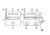
IB族元素、IIIB族元素およびVIB族元素を含む化合物半導体薄膜として、Cu(In、Ga)Se2膜を形成する本発明の1つの実施形態について、図1および図2を参照しながら説明する。図1(a)は、本実施形態の化合物半導体薄膜の製造装置の概略図であり、図1(b)は、図1(a)の装置のX−X’線に沿って切り取った上面図である。図2(a)および(b)は、本実施形態の化合物半導体薄膜の製造方法を説明する概略工程図であり、それぞれ、前駆体薄膜および化合物半導体薄膜が形成された基板の概略断面図を示す。本実施形態は、第1工程として上記の例(1-3)を実施し、第2工程として上記の例(2-3)および(2-4)を実施するものに関する。
【0055】
図1(a)および(b)に示すように、本実施形態の化合物半導体薄膜の製造装置20は、チャンバ1の内部に、VIB族元素の供給源としての蒸着源2と、IB族元素およびIIIB族元素をスパッタリング法を用いて基板上に供給して、IB族元素およびIIIB族元素を含む前駆体薄膜を基板上に形成するための3個のスパッタ源3a、3bおよび3cと、基板5を加熱するためのランプ式ヒーター6とを備える。本実施形態においては、蒸着源2はSe蒸発原料を配置するためのものである。また、スパッタ源3a、3bおよび3cは、IIIB族元素ターゲットであるInターゲット、IB族元素ターゲットであるCuターゲット、ならびにIB族元素とIIIB族元素とからなるターゲットであるCu−Gaターゲットを各々配置するためのものであるが、これら3つのターゲットは、3つのスパッタ源3a、3bおよび3cにどのような組合せで配置されてもよい。
【0056】
本実施形態においては、3つのターゲットをスパッタリングして前駆体薄膜を形成するために3つのスパッタ源を備える装置を示したが、本発明はこれに限定されない。前駆体薄膜の形成様式によっては1個、2個、または4個以上のターゲットを用いてよく、その場合には、ターゲットの数に応じた数のスパッタ源を備える装置を用いることは、当業者には容易に理解されよう。
【0057】
この装置20においては、カーボン材料からなる均熱板4に取り付けられた基板5が、均熱板4をヒーター6の側にして、サセプタ(またはホルダー)7を用いて支持される。ヒーター6は、均熱板4を介して基板5を均一に加熱し、基板5の膜を形成する側の表面(即ち均熱板4と反対側の露出表面であり、図2を参照して後述する導電膜5aの露出表面)の温度を所望の値に制御することができる。サセプタ7は回転駆動軸8に連結されており、回転駆動軸8を回転させることによって、サセプタ7が回転し、基板5および均熱板4を自転させる。更に、チャンバ1内には、基板5の表面への各原料粒子(Cu、In、Ga、およびSe)の供給を制御するように、蒸着源2、スパッタ源3a、スパッタ源3bおよびスパッタ源3cと、基板5との間に配置されたシャッター9が備えられる。スパッタ源3a、3bおよび3cには、スパッタ源に電圧が印加されていないときに、蒸着源2から蒸発するSeが各スパッタ源3a〜3cに備えられるターゲットに付着することを防ぐため、例えばスライド開閉式のシャッターなどのスパッタ源シャッター3A、3Bおよび3C(図1(a)および(b)に点線にて示す)がそれぞれ備えられる。均熱板4、回転駆動軸8、およびシャッター9は、本発明の実施に必ずしも必要ではないが、これらを備えていることが好ましい。
【0058】
スパッタ源3a、3bおよび3cの各々は、接地されたDC電源(図示せず)にスイッチング可能に接続され、これにより電圧印加が制御される。尚、DC(直流)電源に代えてRF(高周波)電源を用いてもよく、この場合には、RF電源は整合器およびコンデンサなどと共に用いられ得る。チャンバ1には、チャンバ1内を真空排気するための排気ライン10と、チャンバ1内にArガスを供給するためのArガスライン11とが連結されている。
【0059】
次に、このような装置20を用いる本実施形態の化合物半導体薄膜の製造方法について説明する。
【0060】
1.準備
まず、図2を参照して示すようなMoなどからなる導電膜5aが、ガラスからなる基板本体5b上に形成された基板5を、図1に示す均熱板4に、基板本体5b側が均熱板4に接触するようにして取り付ける。他方、チャンバ1を排気ライン10からポンプ(図示せず)などを用いて真空排気する。このチャンバ1において、均熱板4に取り付けた基板5をサセプタ7に、図1に示すように設置し、Se蒸発原料、Inターゲット、CuターゲットおよびCu―Gaターゲットをそれぞれ蒸着源2、スパッタ源3a、スパッタ源3bおよびスパッタ源3cに設置する。このとき、各スパッタ源には電圧が印加されておらず、スパッタ源シャッター3A〜3Cおよびシャッター9は閉じておく。
【0061】
次に、ヒーター6を用いて均熱板4を介して基板5を均一に加熱し、基板5のMo膜5aの表面が例えば約20〜450℃、好ましくは約300〜400℃となるように加熱を制御し、他方、Arガス供給ライン11よりチャンバ1内にArガスを供給し始める。基板5が所定の温度に達してほぼ一定温度になると、回転駆動軸8を回転させてサセプタ7を回転させ、これにより基板5および均熱板4を自転させる。このとき、Arガスの供給を維持したまま、チャンバ1内の圧力を所定の圧力に保つように、Arガスの供給および排気を制御する。
【0062】
2.工程(a)
2−1.第1工程
その後、Inターゲットが設置されたスパッタ源3aのスパッタ源シャッター3Aを開き、スパッタ源3aを電源に接続して電圧を印加し、ならびに、Se蒸発原料が設置された蒸着源2を加熱する。このとき、必要に応じてプリスパッタを行ってInターゲット表面をクリーニングするようにしてもよい。InおよびSeが安定に放出されるようになるとシャッター9を開いて、第1工程としてInをスパッタリング法により、ならびにSeを蒸着法により基板5の表面に供給する。所定時間経過後、例えば3〜60分後にシャッター9およびスパッタ源シャッター3Aを閉じ、スパッタ源3aの電圧印加を停止してInの放出を終了する。この第1工程によって、基板5のMo膜5a上にIn−Seからなる第1層12(図2(a)を参照のこと)が形成される。
【0063】
2−2.第2工程
次に、第1工程に引き続いてSe蒸着源2の加熱を維持したまま、CuターゲットおよびCu−Gaターゲットがそれぞれ設置されたスパッタ源3bおよび3cのスパッタ源シャッター3Bおよび3Cを開き、スパッタ源3bおよび3cを各々電源に接続して電圧を印加する。このとき、必要に応じてプリスパッタを行ってCuターゲットおよびCu−Gaターゲット表面をクリーニングするようにしてもよい。CuおよびGaが安定に放出されるようになるとシャッター9を開いて、第2工程としてSeを蒸着法により、CuおよびGaをスパッタリング法により基板5の表面、より詳細には第1層12の上に供給する。所定時間経過後、例えば1〜30分後にシャッター9ならびにスパッタ源シャッター3Bおよび3Cを閉じ、スパッタ源3bおよび3cの電圧印加を停止してCuおよびGaの放出を終了する。この第2工程によって、第1層12の上にCu−Ga−Seからなる第2層13(図2(a)を参照のこと)が形成される。
【0064】
以上のようにして、第1工程および第2工程を経て、図2(a)に示すような第1層12および第2層13が順次積層された前駆体薄膜14が形成される。
【0065】
3.工程(b)
上記の工程(a)により前駆体薄膜14を形成した後、第1および第2工程に引き続いてSe蒸着原2の加熱を維持したままで、好ましくはArガスの供給を停止し、再びシャッター9を開いてSeを蒸着法により前駆体薄膜14の表面に供給する。このようにしてSeを供給しながら、基板5のMo膜5aの表面の温度が前駆体薄膜形成時よりも高い温度、例えば約300〜600℃で、かつ工程(a)におけるよりも高い温度、好ましくは約450〜550℃となるようにヒーター6からの加熱を制御する。所定時間経過後、好ましくは約1秒〜10分後、ヒーター6の加熱を停止する。その後、基板温度が工程(a)付近の温度まで低下すると、シャッター9を閉じ、蒸着源2の加熱を停止してSeの放出を終了する。この工程によって、Seが前駆体薄膜14中に取り込まれると共に化合物が形成され、前駆体薄膜14からCu(In、Ga)Se2薄膜15(図2(b)を参照のこと)が形成される。
【0066】
以上のような工程(a)および(b)により、図2(b)に示すようなCu(In、Ga)Se2からなる化合物半導体薄膜15が形成される。
【0067】
得られた化合物半導体薄膜15は、3cm×3cm以上、更には10cm×10cm、より更に30cm×30cm以上の大きい面積に亘って、約0.01〜0.5μmの範囲、更には0.01〜0.3μmの範囲の表面ラフネスを有する。この値は比較的小さい値であり、化合物半導体薄膜が滑らかな表面を有することがわかる。
【0068】
本実施形態によれば、工程(a)においてスパッタリング法を用いて前駆体薄膜を形成し、次いで、工程(b)でSeを供給しながら熱処理している。このような方法においては、従来の蒸着法のみを用いて化合物半導体薄膜を形成する方法よりも化合物半導体薄膜の膜厚を大面積に亘って均一とすることができる。
【0069】
また、本実施形態によれば、VIB族元素であるSeをスパッタリング法を用いて供給せず、蒸着法を用いて供給し、更に工程(a)において形成された前駆体薄膜に熱処理を施しているので、従来のスパッタリング法のみを用いて一段階で化合物半導体薄膜を形成する方法に比べて化合物半導体薄膜に導入される結晶欠陥が減少する。尚、本実施形態に代えて、工程(a)においてSeをCu−Seターゲットなどを用いてスパッタリングにより供給することも可能であるが、その場合には、続く工程(b)での熱処理により前駆体薄膜中に導入され得る結晶欠陥が緩和されるので、該従来の方法に比べて化合物半導体薄膜に導入される結晶欠陥が減少する。
【0070】
また、本実施形態によれば、IB族元素(Cu)およびIIIB族元素(In)をスパッタリング法により供給すると同時に、VIB族元素(Se)を蒸着法を用いて供給せず、InおよびSeをCuの供給とは別に供給しているので、再蒸発しやすいInおよびSeを、Cuが相対的に過剰となることなく、十分に反応させて化合物を形成させることができる。これにより、組成ずれが減少した化合物半導体薄膜を形成することができる。
【0071】
更に、本実施形態によれば、基板を高温に維持する時間が、蒸着法を単独で用いる従来の方法に比べて短縮され、消費電力がより小さい、安価な化合物半導体薄膜の製造方法が提供される。この方法は、セレン化水素のような有毒ガスを使用しない安全な製造方法である。
【0072】
加えて、本実施形態によれば、スパッタ源シャッターがスパッタ源に備えられており、スパッタ源を使用しないときにはスパッタ源シャッターで該スパッタ源に備えられるターゲットを覆うことができるので、このときに蒸着源から放出されるVIB族元素(Se)によってスパッタ源が汚染されることが防止できる。
【0073】
本実施形態に従って得られた化合物半導体薄膜は、上述のように、膜厚が大面積に亘って均一で、結晶欠陥の発生が低減され、組成ずれが減少し、表面ラフネスが小さいので、良好な膜質を有し、大面積で高効率の薄膜太陽電池の光吸収層として有利に利用され得る。
【0074】
尚、本実施形態において、第1層として、Inをスパッタリング法により供給すると同時にSeを蒸着法により供給してIn−Se層を形成したが、これに代えて、Seの供給を省略してIn層を形成してもよい。また、本実施形態において、第2層として、CuおよびGaをスパッタリング法により供給すると同時にSeを蒸着法により供給してCu−Ga−Se層を形成したが、これに代えて、Seの供給を省略してCu−Ga層を形成してもよい。
【0075】
更に、本実施形態においてはCu−ターゲットおよびCu−Gaターゲットを用いたが、これに代えて、Cuターゲットを単独で用いるか、Cu−Seターゲットを用いることもできる。Cuターゲットを用いる場合には、第2工程にてCuをスパッタリング法により供給して、第2層としてCu層を形成するか、あるいはCuをスパッタリング法により供給すると同時にSeを蒸着法により供給して、第2層としてCu−Se層を形成してもよい。また、Cu−Seターゲットを用いる場合には、第2工程にてCuおよびSeをスパッタリング法により供給して、第2層としてCu−Se層を形成してもよい。このような方法によっても、本実施形態と同様に、CuInSe2膜を形成することが可能である。
【0076】
また、本実施形態においは、第1工程および第2工程の順に実施して、第1層としてIn−Se層(またはIn層)を、第2層としてCu−Ga−Se層(またはCu−Ga層、Cu層、もしくはCu−Se層)を形成したが、第1工程および第2工程を実施する順序を逆にすることも可能である。即ち、先に第2工程を実施して第1層としてCu−Ga層(またはCu−Ga−Se層、Cu層、もしくはCu−Se層)を形成し、次いで第2工程を実施して第2層としてIn−Se層(またはIn層)を形成してもよい。
【0077】
上述のような改変の他にも、本実施形態は、当業者により種々の改変がなされ得る。例えば、VIB族元素(Se)を供給するために蒸着法を用いたが、その他のスパッタリング法以外の方法を用いることも可能である。また、スパッタリング法を実施するためにArガス以外の適切なガスを用いること、シャッターの開閉タイミングを変更することもできる。
【0078】
(実施形態2)
IB族元素、IIIB族元素、およびVIB族元素を含む化合物半導体薄膜として、Cu(In、Ga)Se2膜を形成する本発明のもう1つの実施形態について、図3を参照しながら説明する。図3(a)および(b)は、本実施形態の化合物半導体薄膜の製造方法を説明する概略工程図であり、それぞれ、前駆体薄膜および化合物半導体薄膜が形成された基板の概略断面図を示す。
【0079】
本実施形態は、III B族元素および VI B族元素を供給して、 III B族元素および VI B族元素から成る第1層を形成する工程(i)と、IB族元素および III B族元素を供給して、IB族元素および III B族元素から成る第2層を形成する工程( ii )と、IB族元素および VI B族元素を供給して、IB族元素および VI B族元素から成る第3層を形成する工程( iii )とを順次実施するものである。尚、これら工程(i)、工程( ii )および工程( iii )は、本明細書に言う第1工程、第2B工程および第2A工程にそれぞれ包含される。本実施形態は、より詳細には、工程(i)として上記の例(1-3)を実施し、工程( ii )として上記の例(2-4)を実施し、工程( iii )として上記の例(2-3)を実施するものに関し、実施形態1にて詳述した化合物半導体薄膜の製造装置(図1(a)および(b))と同様の装置を用いて実施することができる。以下、本実施形態の化合物半導体薄膜の製造方法について、実施形態1と異なる点を中心に説明する。
【0080】
1.準備
まず、実施形態1と同様にして準備を行う。本実施形態においても、基板5のMo膜5aの表面が例えば約20〜450℃、好ましくは約300〜400℃となるように加熱を制御し、チャンバ内の圧力を所定の圧力に保つように、Arガスの供給および排気を制御する。
【0081】
2.工程(a)
2−1.工程(i)
その後、実施形態1の第1工程と同様にして、InおよびSeを、それぞれスパッタリング法および蒸着法により基板5の表面に供給する。この工程(i)によって、基板5のMo膜5a上にIn−Seからなる第1層12(図3(a)を参照のこと)が形成される。
【0082】
2−2.工程( ii )
次に、Se蒸着源の加熱を停止して、Seの供給を停止したこと以外は、実施形態1の第2工程と同様にして、CuターゲットおよびCu−Gaターゲットがそれぞれ設置されたスパッタ源を用いて、CuおよびGaをスパッタリング法により基板の表面、より詳細には第1層12の上に所定時間、例えば1〜30分間供給する。この工程( ii )によって、第1層12の上にCu−Gaからなる第2層16(図3(a)を参照のこと)が形成される。
【0083】
2−3.工程( iii )
続いて、Cuスパッタ源からのCuの放出を維持したままで、Se蒸着源を再び加熱し、工程( iii )として、CuおよびSeを、それぞれスパッタリング法および蒸着法により基板5の表面、より詳細には第2層16の上に所定時間、例えば1〜30分間供給する。この工程( iii )によって、第2層16の上にCu−Seからなる第3層17(図3(a)を参照のこと)が形成される。
【0084】
以上のようにして、工程(i)、工程( ii )、および工程( iii )を経て、図3(a)に示すような第1層12、第2層16、および第3層17が順次積層された前駆体薄膜18が形成される。
【0085】
3.工程(b)
上記の工程(a)により前駆体薄膜18を形成した後、実施形態1の工程(b)と同様にして、基板5のMo膜5aの表面の温度が、前駆体薄膜形成時よりも高い温度に、例えば約300〜600℃で、かつ工程(a)におけるよりも高い温度、好ましくは約450〜550℃となるように加熱を制御し、その後、Seを蒸着法により前駆体薄膜18の表面に供給する。この工程によって、Seが前駆体薄膜18中に取り込まれると共に共に化合物が形成され、前駆体薄膜18からCu(In、Ga)Se2薄膜19(図3(b)を参照のこと)が形成される。
【0086】
以上のような工程(a)および(b)により、図3(b)に示すようなCu(In、Ga)Se2からなる化合物半導体薄膜19が形成される。
【0087】
本実施形態によっても、実施形態1と同様の効果を奏することができる。
【0088】
尚、本実施形態においては、第1層として、In−Se層に代えてIn層を形成してもよく、第2層として、Cu−Ga層に代えてCu−Ga−Se層を形成してもよい。更に、第3層として、Cuをスパッタリング法により供給すると同時にSeを蒸着法により供給してCu−Se層を形成したが、これに代えて、Seの供給を省略してCu層を形成してもよい。
【0089】
また、本実施形態においては、工程(i)、工程( ii )、および工程( iii )の順に実施して、第1層としてIn−Se層(またはIn層)を、第2層としてCu−Ga層(またはCu−Ga−Se層)を、次いで第3層としてCu−Se層(またはCu層)を形成したが、工程(i)、工程( ii )、および工程( iii )を実施する順序を変更することも可能である。例えば、工程(i)を実施して第1層としてIn−Se層(またはIn層)を形成した後、先に工程( iii )を実施してCu−Se層(またはCu層)を形成し、次いで工程( ii )を実施して第3層としてCu−Ga層(またはCu−Ga−Se層)を形成してもよい。あるいは、先に工程( ii )を実施して第1層としてCu−Ga層(またはCu−Ga−Se層)を形成し、次いで工程( iii )を実施してCu−Se層(またはCu層)を形成した後、工程(i)を実施して第1層としてIn−Se層(またはIn層)を形成してもよい。
【0090】
尚、上述の実施形態1および本実施形態2においては、3つのスパッタ源を備える装置を用いてそれぞれ2層および3層からなる前駆体薄膜を形成したが、1つのスパッタ源を備える装置を用いて単層の前駆体薄膜を形成すること、あるいは、2つまたは4つ以上のスパッタ源を備える装置を用いて任意の適切な数の層からなる前駆体薄膜を形成することも当業者には容易に想到され得る。
【0091】
(実施形態3)
IB族元素、IIIB族元素、およびVIB族元素を含む化合物半導体薄膜の製造に利用可能な、もう1つの化合物半導体薄膜の製造装置について、図4を参照しながら説明する。図4は、本実施形態の化合物半導体薄膜の製造装置の概略模式図である。図4中、実施形態1にて説明した装置の部材と同様のものには同様の番号を付し、説明を省略する。
【0092】
図4に示すように、本実施形態の化合物半導体薄膜の製造装置30は、2つのチャンバ1aおよび1bを有する。チャンバ1aの内部には、3つのスパッタ源3a、3bおよび3c(但し、図4においてスパッタ源3cは図示していない)が備えられ、他方、チャンバ1bの内部には、VIB族元素の供給源としての蒸着源2が備えられる。チャンバ1aおよび1bには、それぞれ排気ライン10aおよび10bが連結され、チャンバ1aには、更にArガスライン11が連結されている。チャンバ1aおよび1bの内部には、それぞれランプ式ヒーター6と、サセプタ7と、回転駆動軸8と、シャッター9とが共通して備えられる。
【0093】
本実施形態の製造装置30においては、VIB族元素の供給源である蒸着源2が、スパッタ源3a、3bおよび3cが配置されているチャンバ1aとは別のチャンバ1b内に配置されている。従って、本実施形態においては、スパッタ源と蒸着源とが別々のチャンバに配置されているため、スパッタ源に備えられるターゲットに蒸着源から蒸発して放出されるSeが付着してターゲットを汚染することがないので、各スパッタ源にスパッタ源シャッターを必ずしも設けなくてよい。
【0094】
本実施形態の装置30においては、実施形態1および実施形態2を、チャンバ1aにてスパッタリング法のみを用いて工程(a)を実施し、次いで、基板をチャンバ1aからチャンバ1bに移して、チャンバ1bにて工程(b)を実施するように改変することによって、本発明の化合物半導体薄膜の製造方法を実施することができる。
【0095】
本実施形態の装置によれば、VIB族元素の供給源として蒸着源を用いる場合に、蒸着源とスパッタ源とが隔離されているので、蒸着源を用いて蒸発させたVIB族元素によって、スパッタ源に備えられるターゲット表面が汚染されることを防止することができる。
【0096】
尚、本実施形態においては、工程(a)を実施するためのチャンバは、3つのスパッタ源を備えるが、必要に応じて1つ、2つまたは4つ以上のスパッタ源を備えていてもよい。
【0097】
また、本実施形態においては、スパッタ源を収容するチャンバと蒸着源を収容するチャンバとから成る2つのチャンバを備える装置を示したが、1つのチャンバ内に仕切り板を設けて、スパッタ源と蒸着源とを仕切るように改変することも可能である。
【0098】
(実施形態4)
IB族元素、IIIB族元素、およびVIB族元素を含む化合物半導体薄膜の製造に利用可能な、もう1つの化合物半導体薄膜の製造装置について、図5を参照しながら説明する。図5は、本実施形態の化合物半導体薄膜の製造装置の模式的な上面図である。
【0099】
図5に示すように、本実施形態の化合物半導体薄膜の製造装置40は、中央のチャンバ41と、このチャンバ41の周りに隣接し、互いに隔離されたチャンバ42〜47を備える。チャンバ42は基板を入れるロード室であり、チャンバ47は基板を取り出すアンロード室である。チャンバ43〜45は、それぞれ1つのスパッタ源(図示せず)を備えること以外は、図4に示す装置30のチャンバ1aと同様の構成を有するものとし、また、チャンバ46は、図4に示す装置30のチャンバ1bと同様の構成を有するものとする。従って、本実施形態においては、スパッタ源と蒸着源とが別々のチャンバに個々に配置されているため、スパッタ源に備えられるターゲットに蒸着源から蒸発して放出されるSeが付着してターゲットを汚染することがないので、各スパッタ源にスパッタ源シャッターを必ずしも設けなくてよい。
【0100】
このような装置40においては、実施形態2にて詳述した第1〜3層から成る前駆体薄膜の各層を別々のチャンバ内で形成するように改変することによって、本発明の化合物半導体薄膜の製造方法を実施することができる。具体的には、まず、チャンバ42に設置された基板をチャンバ41を経由してチャンバ43に移して第1層を形成し、次いでチャンバ41を経由してチャンバ44に移して第2層を形成し、次いでチャンバ41を経由してチャンバ45に移して第3層を形成して前駆体薄膜を形成し、次いでチャンバ41を経由してチャンバ44に移して工程(b)を実施して所望の化合物半導体薄膜を形成し、最後に、化合物半導体薄膜が形成された基板をチャンバ41を経由してチャンバ47に移し、ここから取り出される。このように、本実施形態の装置を用いても本発明の化合物半導体薄膜の製造方法を基板を中央のチャンバを介して移動させながら実施することができる。
【0101】
本実施形態の装置によれば、実施形態3の装置によって得られる効果に加えて、スパッタ源同士が隔離されているので、他のスパッタ源から放出される粒子によってスパッタ源に備えられるターゲット表面が汚染されることを防止することができる。
【0102】
更に、本実施形態の装置によれば、複数枚の基板を別々のチャンバ内で同時に処理することができるので、成膜タクトを短縮すること(または単位時間あたりの処理枚数をより多くすること)ができる。
【0103】
(実施形態5)
IB族元素、IIIB族元素、およびVIB族元素を含む化合物半導体薄膜の製造に利用可能な、もう1つの化合物半導体薄膜の製造装置について、図6を参照しながら説明する。図6は、本実施形態の化合物半導体薄膜の製造装置の模式的な上面図である。
【0104】
図6に示すように、本実施形態の化合物半導体薄膜の製造装置50は、チャンバ51と、このチャンバ51の内部にて仕切り板52を介して隣接して配置された内部チャンバ53〜58を備える。内部チャンバ53は基板を入れるロード室であり、内部チャンバ58は基板を取り出すアンロード室である。チャンバ54〜56は、図5に示す装置40のチャンバ43〜45と同様の構成を有するものとし、また、チャンバ57は、図5に示す装置40のチャンバ46と同様の構成を有するものとする。ここで、本実施形態においては、スパッタ源と蒸着源とが個々に仕切られて配置されているので、実施形態4と同様に、各スパッタ源にスパッタ源シャッターを必ずしも設けなくてよい。
【0105】
このような装置50においては、実施形態2にて詳述した第1〜3層から成る前駆体薄膜の各層を別々のチャンバ内で形成するように改変することによって、本発明の化合物半導体薄膜の製造方法を実施することができる。具体的には、まず、内部チャンバ53に設置された基板をチャンバ54に移して第1層を形成し、次いで内部チャンバ55に移して第2層を形成し、次いで内部チャンバ56に移して第3層を形成して前駆体薄膜を形成し、次いで内部チャンバ57に移して工程(b)を実施して所望の化合物半導体薄膜を形成し、最後に、化合物半導体薄膜が形成された基板を内部チャンバ58に移し、ここから取り出される。このように、本実施形態の装置を用いても本発明の化合物半導体薄膜の製造方法を基板を公転して移動させながら実施することができる。
【0106】
本実施形態の装置によれば、実施形態4の装置によって得られる効果と同様に、成膜タクトを短縮することができる。
【0107】
尚、上述の実施形態4および本実施形態5においては、それぞれ1つのスパッタ源を備える3つのチャンバを示したが、必要に応じてチャンバの数および各チャンバに備えられるスパッタ源の数を選択することも可能である。
【0108】
【実施例】
上述の実施形態1の装置を用いて、Cu−Gaターゲットを用いない点を除いて実施形態1と同様の製造方法を実施して、化合物半導体薄膜としてCuInSe2膜を形成した。即ち、本実施例においては、IIIB族元素ターゲットであるInターゲットと、IB族元素ターゲットであるCuターゲットのみをスパッタ源にそれぞれ設置して用いるものとした。
【0109】
本実施例では、厚さ約0.55mmのソーダライムガラス基板本体と、その上面に形成された厚さ約0.8μmのMo導電膜とからなる基板を用いた。
【0110】
まず、実施形態1の工程(a)において、上記の基板上に、第1工程としてInをスパッタリングにより供給すると同時にSeを蒸着法により供給してIn−Se層を形成した。次いで第2工程としてCuをスパッタリングにより供給すると同時にSeを蒸着法により供給してCu−Se層を形成した。これにより、In−Se層およびCu−Se層が、基板上に順次積層形成された前駆体薄膜を得た。これら第1工程および第2工程を含む工程(a)は、基板温度(より詳細にはMo導電膜温度)を約200〜350℃に維持して実施した(図7を参照のこと)。
【0111】
次いで、実施形態1の工程(b)において、図7に示すように、Seを蒸着法により前駆体薄膜上に供給しながら、まず、基板を加熱して上記基板温度を約1秒〜5分間で約400〜500℃にまで上昇させて熱処理し、次いで、加熱を停止して基板を放冷した。基板温度が先の工程(a)における温度に達するまで、即ち約200〜350℃に達するまでSeの供給を続け、その後、供給を停止した。これにより、Cu−In−Se化合物半導体薄膜が基板上に形成された。
【0112】
得られた化合物半導体薄膜は、エネルギー分散型X線測定により、Cu 22.7原子%、In 26.25原子%、Se 51.4原子%の組成割合を有することが解った。この分析値は、CuInSe2膜の化学量論比に対してややInおよびSeが過剰な組成比(具体的にはCu:Inが約0.8〜1.0)であって、太陽電池の光吸収層として用いるのに適した目的の組成比にほぼ等しかった。
【0113】
この化合物半導体薄膜を光吸収層として、当該技術分野において既知の常套の方法により、CdS層(バッファ層)、ZnO層およびITO膜(いずれも透明導電膜)を得られた化合物半導体薄膜上に順次積層し、基板のMo導電膜およびITO膜からそれぞれリードを引き出して薄膜太陽電池を作製した。この薄膜太陽電池は、変換効率9.06%、電流密度36.16mA/cm2、開放電圧0.40V、曲性因子0.62を示し、従来の製造方法に従って得られたCu、In、およびSeからなる化合物半導体薄膜を備える薄膜太陽電池の特性と比較して高いレベルにあった。
【0114】
【発明の効果】
本発明によれば、IB族元素、IIIB族元素、およびVIB族元素を含む化合物半導体薄膜の製造方法であって、膜厚が大面積に亘って均一で、組成ずれが減少し、結晶欠陥の発生が低減された、安価で安全な製造方法が提供される。更に、本発明によれば、このような製造方法を実施するのに好適に用いられる装置が提供される。本発明の方法に従って、本発明の装置を用いて得られた化合物半導体薄膜は、良好な膜質を有し、大面積で高効率の薄膜太陽電池の光吸収層として利用され得る。
【図面の簡単な説明】
【図1】 図1(a)は、本発明の1つの実施形態における化合物半導体薄膜の製造装置の概略図であり、図1(b)は、図1(a)の装置のX−X’線に沿って切り取った上面図である。
【図2】 図2(a)および(b)は、本発明の1つの実施形態における化合物半導体薄膜の製造方法であって、図1の装置を用いて実施される方法を説明する概略工程図であり、それぞれ、前駆体薄膜および化合物半導体薄膜が形成された基板の概略断面図を示す。
【図3】本発明のもう1つの実施形態における化合物半導体薄膜の製造方法を説明する概略工程図であり、図3(a)および(b)は、前駆体薄膜および化合物半導体薄膜が形成された基板の概略断面図をそれぞれ示す。
【図4】 本発明の別の実施形態における化合物半導体薄膜の製造装置の概略図である。
【図5】 本発明の別の実施形態における化合物半導体薄膜の製造装置の概略図である。
【図6】 本発明の別の実施形態における化合物半導体薄膜の製造装置の概略図である。
【図7】 本発明の1つの実施例における基板温度のプロファイルを示すグラフである。
【符号の説明】
1 チャンバ
2 蒸着源
3a、3b、3c スパッタ源
3A、3B、3C スパッタ源シャッター
4 均熱板
5 基板
6 ヒーター
7 サセプタ
8 駆動回転軸
9 シャッター
10 排気ライン
11 Arガス供給ライン
20 化合物半導体薄膜製造装置[0001]
BACKGROUND OF THE INVENTION
The present invention relates to a method and apparatus for producing a compound semiconductor thin film and a compound semiconductor thin film obtained therefrom. More specifically, the present invention relates to a method and apparatus for producing a compound semiconductor thin film containing a group IB element, a group IIIB element, and a group VIB element used in the field of thin film solar cells, and a compound semiconductor thin film obtained therefrom.
[0002]
[Prior art]
In recent years, a compound semiconductor thin film having a chalcopyrite structure composed of a group IB element, a group IIIB element and a group VIB element has been used as a light absorption layer constituting a thin film solar cell. As such a compound semiconductor thin film, for example, CuInSe2Film (so-called “CIS” film), CuInGaSe2Film (specifically Cu (In, Ga) Se2Membranes, so-called “CIGS” membranes).
[0003]
Conventional manufacturing methods of such a compound semiconductor thin film are generally roughly classified into a method using a vapor deposition method and a method using a sputtering method. Hereinafter, as an example of these methods, CuInSe2Several typical methods for forming a film will be described.
[0004]
As a conventional method using a vapor deposition method, there is a method in which constituent elements of a target compound semiconductor thin film are supplied in multiple steps onto a high-temperature substrate by a vapor deposition method. In this method, a vapor deposition source in which a Cu evaporation source, an In evaporation source, and a Se evaporation source are installed, respectively, and a glass substrate having, for example, a Mo film on its upper surface is kept at room temperature in a vacuum chamber maintained at a predetermined pressure. In the state heated to a higher temperature of about 325 ° C., first, as a first stage, the In evaporation source and the Se evaporation source are heated and evaporated, and In and Se are supplied onto the substrate. An In—Se layer is formed. Next, as a second stage, the substrate is further heated to a high temperature of about 500 to 600 ° C., and in this state, the Cu evaporation source and the Se evaporation source are heated and evaporated, and Cu and Se are respectively supplied by a vapor deposition method. . At this time, since the substrate is in a high temperature state, Cu and Se supplied to the surface of the In—Se layer are not stacked on the In—Se layer but are taken into the In—Se layer to form a compound, Thereby, a Cu—In—Se compound layer grows. Finally, as a third stage, with the substrate kept at a high temperature, the In evaporation source and the Se evaporation source are heated and evaporated, and In and Se are respectively supplied by a vapor deposition method. Even at this stage, Cu and Se supplied to the surface of the Cu—In—Se layer are taken into this layer to form a compound, and the Cu—In—Se compound layer grows, and finally CuInSe.2A film is formed.
[0005]
On the other hand, as a conventional method using the sputtering method, there is a method of supplying the constituent elements of the target compound semiconductor thin film onto the substrate in one step by the sputtering method. In this method, for example, a sputtering source in which a Cu target, an In target, and an Se target are respectively installed is provided, and each target is sputtered in a vacuum chamber maintained at a predetermined pressure, so that the above-described substrate is formed. Cu, In, and Se are simultaneously supplied to CuInSe.2A film is grown and formed. As the target, a target made of any combination of materials selected from the group consisting of Cu, In, and Se can also be used.
[0006]
Further, as another conventional method using the sputtering method, a constituent element other than Se of the target compound semiconductor thin film is supplied onto the substrate in multiple stages by the sputtering method to form a laminated film, and then hydrogen selenide ( H2There is a method of heat-treating a substrate in an Se) atmosphere. In this method, first, in a vacuum chamber maintained at a predetermined pressure, for example, a Cu target is sputtered onto the substrate as described above to supply Cu, and then an In target is sputtered to supply In. Thereby, a Cu film and an In film are sequentially formed to form a laminated film. Next, the obtained substrate is heated to about 500 ° C. in a hydrogen selenide atmosphere and subjected to heat treatment (also referred to as Se conversion treatment). At this time, the laminated film composed of the Cu film and the In film takes in Se and grows while forming a compound, and finally, CuInSe2A film is formed.
[0007]
In addition to the above-described method, there is a method in which constituent elements other than Se of the target compound semiconductor thin film are supplied onto the substrate in one step by sputtering, and simultaneously, Se is deposited by evaporation. In this method, in a vacuum chamber maintained at a predetermined pressure, for example, a Cu target and an In target are sputtered, and Cu and In are respectively supplied onto the substrate as described above in one step, and at the same time, Se. The evaporation material is heated to evaporate, and Se is supplied by an evaporation method. As a result, Cu, In, and Se are simultaneously supplied, and CuInSe2The film grows.
[0008]
CuInSe2Although the method of forming the film has been described in detail, CuInGaSe2A film and a similar thin film can be formed in substantially the same manner.
[0009]
[Problems to be solved by the invention]
In recent years, further increase in capacity (larger area), higher efficiency, and lower cost of thin film solar cells are desired. Accordingly, even for compound semiconductor thin films containing a group IB element, a group IIIB element, and a group VIB element used as a light absorption layer of a thin film solar cell, a thin film having a uniform and uniform film thickness over a large area. Establishment of forming technology is desired.
[0010]
However, none of the conventional methods for producing a compound semiconductor thin film as described above sufficiently satisfy such a demand.
[0011]
In the conventional manufacturing method using the vapor deposition method alone, generally, as a vapor deposition source, for example, a crucible around which a heater such as a metal wire is wound is used, an evaporation raw material is put into this crucible, and resistance heating is used under vacuum. The evaporation material is heated to evaporate, but such a method has a problem that the evaporation rate (or the evaporation rate or the supply rate) of the evaporation material changes depending on the amount of the evaporation material in the crucible. For this reason, in order to obtain a constant evaporation rate, it is preferable to control by appropriately changing the current passed through the heater according to the evaporation / consumption of the evaporation raw material, but such control is actually difficult. In addition, in the vapor deposition method using such a vapor deposition source, it is difficult to form a thin film with a uniform thickness on a large-area substrate. In addition to this, in the vapor deposition method, it is necessary to heat the substrate in a high temperature state (for example, about 500 to 600 ° C.) for a long time (for example, about 10 to 90 minutes). high.
[0012]
On the other hand, in the conventional manufacturing method using the sputtering method alone, the target of the raw material element is generally installed in the sputtering source, and the target is sputtered and evaporated by Ar ions or the like under vacuum. According to this method, since the fluctuation of the evaporation rate is small, it is easy to form a thin film with a uniform thickness on a large-area substrate as compared with the method using the evaporation method as described above. High controllability. However, when the VIB group element is supplied by the sputtering method, a part of the VIB group element released by sputtering evaporation from the VIB group element (or including it) target is negatively ionized, and the negative ionized VIB group element is formed into a film. There is a problem in that the surface is impacted to cause defects in the film.
[0013]
Further, according to the above-described conventional manufacturing method in which a laminated film is formed by sputtering and then heat-treated (or Se-treated) in a hydrogen selenide atmosphere, the defects as described above are alleviated by heat treatment after sputtering. The film quality can be improved. However, hydrogen selenide used in this method is a toxic gas, and the production is carried out in a work environment with high risk. Furthermore, it is necessary to install special incidental equipment such as a detoxification device in order to dispose of hydrogen selenide used in Se treatment and hydrogen as a by-product in the atmosphere. Installation of such equipment And additional costs for maintenance.
[0014]
On the other hand, according to the above-described conventional manufacturing method in which constituent elements other than Se are supplied onto the substrate in one step by a sputtering method and simultaneously by a vapor deposition method, the VIB group element is not a sputtering method but a vapor deposition method. Since it can be supplied, the problem of defect formation can be avoided, and furthermore, since toxic hydrogen selenide is not used, the production can be carried out in a safer working environment. However, in this method, since the IB group element and the IIIB element other than the VIB group element are supplied by the sputtering method and the VIB group element is supplied by the vapor deposition method, for example, Cu as the IB group element, In as the IIIB group element, and In / When using S and / or Se as a Ga, VIB group element, the low melting point group IIIB and VIB group elements are re-evaporated and insufficient, and the relatively high melting point group IB element is excessive, This causes a new problem that compositional deviation (that is, formation of a compound having a composition deviated from the composition of the target compound) is likely to occur as compared with other methods.
[0015]
The phenomenon in which such a composition shift occurs is, for example, when Cu is used as the IB group element, In is used as the IIIB group element, and Se is used as the VIB group element. And Se are high melting point In on the substrate supply surface.2SeThreeSince the compound phase was initially formed, it was not seen because the low-melting elements (in this case In and Se) were prevented from re-evaporating. However, when Se is supplied by a vapor deposition method and Cu and In are simultaneously supplied by a sputtering method, the energy of Se particles supplied by the vapor deposition method is compared with the energy of In particles supplied by the sputtering method. Much smaller, In2SeThreeSince it becomes difficult to form a compound phase, more In and Se are re-evaporated than when all elements are supplied by the sputtering method, while the high melting point Cu supplied simultaneously with In and Se is regenerated. Since evaporation hardly occurs, it is relatively excessive with respect to In and Se. As a result, it is considered that a large composition shift tends to occur in some cases in a method in which sputtering and vapor deposition are simultaneously used and supplied onto the substrate in only one stage.
[0016]
This problem of compositional deviation also occurs when Ga is used as the IIIB group element and S is used as the VIB group element. This is because Ga and S also have a low melting point and are easily re-evaporated.
[0017]
The present invention has been made to solve the conventional problems as described above, and an object of the present invention is a method for producing a compound semiconductor thin film containing a group IB element, a group IIIB element and a group VIB element, A novel manufacturing method that at least partially ameliorates conventional problems such as non-uniform film thickness over a large area, occurrence of large compositional deviations, generation of crystal defects, high risk of working environment, high manufacturing cost, etc. Another object of the present invention is to provide an apparatus capable of carrying out such a method, and a compound semiconductor thin film obtained thereby.
[0018]
Throughout this specification, the term “sputtering method” refers to accelerating ionized gas atoms (for example, Ar ions) and using this to release raw material particles from a target of a raw material element provided in a sputtering source by a sputtering phenomenon ( (Or sputtering evaporation). The “evaporation method” refers to a method of evaporating raw material particles by heating an evaporation material provided in an evaporation source under a so-called vacuum.
[0019]
[Means for Solving the Problems]
The method of the present invention is a method for producing a compound semiconductor thin film containing a group IB element, a group IIIB element, and a group VIB element, comprising: (a) supplying at least a predetermined raw material element on a substrate using a sputtering method; Forming a precursor thin film containing a group IB element and a group IIIB element or a precursor thin film containing a group IB element, a group IIIB element and a group VIB element on a substrate; and (b) using a method other than sputtering. While supplying the VIB group element onto the precursor thin film, the substrate on which the precursor thin film is formed is heat-treated at a temperature higher than the temperature in the step (a), and from the precursor thin film, the group IB element, group IIIB Forming a compound semiconductor thin film containing an element and a VIB group element on a substrate.
[0020]
According to the method of the present invention as described above, since the precursor thin film is formed by using the sputtering method in the step (a), the thickness of the compound semiconductor thin film obtained therefrom is uniform over a large area. It is suitable for forming a compound semiconductor thin film on a large-area substrate.
[0021]
Furthermore, according to the method of the present invention, since it is not necessary to supply the VIB group element using a sputtering method, the introduction of crystal defects resulting from the ionization of the VIB group element is reduced in the compound semiconductor thin film. However, the method of the present invention optionally includes supplying the group VIB element using a sputtering method in step (a), in which crystal defects may be introduced into the precursor thin film, but the subsequent step ( In b), since the VIB group element is supplied onto the precursor thin film using a method other than sputtering and the substrate is heat-treated at a high temperature, the introduced crystal defects can be relaxed and reduced. Therefore, the generation of crystal defects is reduced by the method of the present invention.
[0022]
Further, according to the method of the present invention, the time for maintaining the substrate at a high temperature is shortened as compared with the conventional method using the vapor deposition method alone. This provides an inexpensive method for manufacturing a compound semiconductor thin film with relatively low power consumption. This method is a safe manufacturing method that does not use a toxic gas such as hydrogen selenide, and there is no need to provide incidental equipment.
[0023]
In the present invention, the group IB element, the group IIIB element and the group VIB element can be arbitrarily selected based on the periodic table. For example, the group IB element is either or both of Ag and Cu, and the group IIIB The element can be either or both of In and Ga, and the VIB group element can be either or both of Se and S. More preferably, the group IB element is Cu, the group IIIB element is In, or In and Ga, the group VIB element is Se, and CuInSe containing these elements2Film or Cu (In, Ga) Se2The film is manufactured according to the method of the present invention as a compound semiconductor thin film. However, the present invention is not limited to this, and other compound semiconductor thin films (for example, CuInS)2, CuGaSe2, CuGaS2, Cu (In, Ga) S2, Cu (In, Ga) (S, Se)2, CuInThreeSeFive, CuInThreeSFive, CuGaThreeSeFive, CuGaThreeSFive, Cu (In, Ga)ThreeSeFive, Cu (In, Ga)ThreeSFive, And Cu (In, Ga)Three(S, Se)FiveOr a compound semiconductor thin film in which a small amount of other elements are dissolved in addition to the IB group element, the IIIB group element and the VIB group element.
[0024]
In the present invention, the “precursor thin film” refers to a semiconductor layer before the target compound semiconductor thin film is formed, and may be a multilayer or a single layer depending on the formation mode of the precursor thin film and the substrate temperature at this time. This precursor thin film contains a group IB element and a group IIIB element, and may or may not contain a group VIB element.
[0025]
The “method other than the sputtering method” refers to a method of supplying a target raw material element to a predetermined place other than the sputtering method. Examples of such a method include a vapor deposition method, laser ablation, proximity sublimation method, and the like, and a method of using these in any combination, and a vapor deposition method is preferable.
[0026]
As a substrate that can be used in the present invention, for example, a glass substrate, a metal substrate, a metal film, a resin substrate, a resin film, or the like can be used. Further, such a substrate is used as a substrate body on which, for example, Mo, MoSe.2, Pt, Au, Cr, Ni, AgPdCu, WSi, etc., and in particular when a glass substrate, a transparent metal film or a resin film is used, the conductive film made of such a material. Instead, ITO, ZnO: Al, SnO2A transparent conductive film such as ZnO and a window layer such as ZnO may be provided.
[0027]
Hereinafter, the method of the present invention will be described in detail.
[0028]
In the step (a), a precursor thin film containing a group IB element and a group IIIB element, or a group IB element, by supplying a predetermined raw material element onto the substrate using at least a sputtering method, A precursor thin film containing a group IIIB element and a group VIB element is formed on the substrate.
[0029]
In a preferred embodiment, the temperature of the substrate in step (a) is in the range of 20 to 450 ° C, more preferably in the range of 300 to 400 ° C.
[0030]
Here, a method of supplying a group IB element and a group IIIB element using a sputtering method includes a target composed of a group IB element (for example, a Cu target), a target composed of a group IIIB element (for example, an In target), and a group IB element. A target composed of a group IIIB element (for example, a Cu-Ga target), a group composed of a group IB element and / or a group IIIB element and an element other than these elements (for example, a group VIB element) (for example, a Cu-Se target, In- (Se target, Cu-In-Se target, Cu-Ga-Se target) may be sputtered.
[0031]
At this time, in order to form the precursor thin film, not only the IB group element and the IIIB group element (and possibly other elements) are supplied using the sputtering method, but also a method other than the sputtering method is used in combination. May be. For example, the IB group element and / or the IIIB group element may be supplied by a sputtering method, and the VIB group element may be supplied by a method other than the sputtering method such as an evaporation method. In addition, for example, the IB group element and / or the IIIB group element may be supplied by a sputtering method, and at the same time, the same kind of element may be supplied by a method other than the sputtering method such as an evaporation method.
[0032]
In a preferred embodiment, the step (a) includes a first step of supplying a group IIIB element or supplying a group IIIB element and a group VIB element, and a group IB element and a group VIB element supplying a group IB element. Supplying, supplying a group IB element and a group IIIB element, or supplying a group IB element, a group IIIB element and a group VIB element.
[0033]
In this aspect, the order of performing the first step and the second step may be the second step after the first step is performed or vice versa.
[0034]
According to this aspect, although depending on the temperature of the substrate, a structure of two or more layers comprising the layer formed by the first step and the layer formed by the second step (however, the first step and the second step are respectively When implemented in one step, a precursor thin film having a two-layer structure can be formed on the substrate.
[0035]
Further, according to this aspect, the group IB element and the group IIIB element are supplied by the sputtering method, and at the same time, the group VIB element is supplied by the vapor deposition method, so that it is not formed in one step. Even when In and / or Ga is used as a group element and Se and / or S is used as a VIB group element, a compound semiconductor thin film having a desired composition can be formed without causing a large composition shift.
[0036]
The first step can be performed, for example, as follows.
(1-1) A group IIIB element target (for example, an In target) is used to supply a group IIIB element by a sputtering method.
(1-2) Supplying a Group IIIB element and a Group VIB element by sputtering using at least one target (for example, an In-Se target and, if necessary, an In target) containing a Group IIIB element and a Group VIB element Or
(1-3) A group IIIB element is supplied by a sputtering method using a group IIIB element target (for example, an In target), and at the same time a group VIB element is deposited by a vapor deposition method using a group VIB element evaporation source (for example, an Se evaporation source). Supply.
[0037]
Moreover, the said 2nd process can be implemented as follows, for example.
(2-1) supplying a group IB element by a sputtering method using a group IB element target (for example, a Cu target);
(2-2) Supplying a group IB element and a group VIB element by a sputtering method using at least one kind of target (for example, a Cu-Se target and, if necessary, a Cu target) containing a group IB element and a group VIB element ,
(2-3) A group IB element is supplied by sputtering using a group IB element target (for example, Cu target), and simultaneously a group VIB element is deposited by vapor deposition using a group VIB element evaporation source (for example, Se evaporation source). Supply,
(2-4) IB group elements and IIIB group elements are supplied by sputtering using at least one target (for example, a Cu-Ga target and optionally a Cu target) containing a group IB element and a group IIIB element. ,
(2-5) Using at least one kind of target (for example, Cu-In-Se target or Cu-Ga-Se target) containing a group IB element, a group IIIB element, and a group VIB element, a group IB element, a group IIIB element, and Supply VIB group elements by sputtering, or
(2-6) Supplying a group IB element and a group IIIB element by a sputtering method using at least one kind of target containing a group IB element and a group IIIB element (for example, a Cu-Ga target and, if necessary, a Cu target). At the same time, the VIB group element is supplied by vapor deposition using the VIB group element evaporation raw material (for example, Se evaporation raw material).
[0038]
The first step and the second step are independent of each other from the above-mentioned first step examples (1-1) to (1-3) and the second step examples (2-1) to (2-6). One or more can be selected, and can be implemented in any appropriate combination depending on the constituent elements of the compound semiconductor thin film to be formed. The above example (1-1) or (1-2) as the first step, the above example (2-2) and / or (2-4) as the second step, or the above as the first step The combination of Example (1-3) and Example (2-3) and / or (2-4) above is preferable as the second step.
[0039]
In a preferred embodiment, the second step includes supplying a group IB element, or supplying a group IB element and a VIB element, step A, supplying a group IB element and a group IIIB element, or providing a group IB element, And a second B step of supplying a group IIIB element and a group VIB element.
[0040]
In this embodiment, the first step, the second A step, and the second B step can be performed in any appropriate combination order. Specifically, (first process, 2A process, 2B process), (first process, 2B process, 2A process), (2A process, 2B process, 1st process), (2B process) You may implement in any order of a process, 2A process, 1st process), (2A process, 1st process, 2B process), and (2B process, 1st process, 2A process).
[0041]
In this aspect, the second step in the above-described aspect is performed in two stages. According to this aspect, although it depends on the temperature of the substrate, a structure of three or more layers comprising a layer formed by the first step, a layer formed by the second A step, and a layer formed by the second B step (however, When the first step, the second A step, and the second B step are each performed in one step, a precursor thin film having a three-layer structure can be formed on the substrate.
[0042]
The second 2A step can be performed, for example, by any one of the above (2-1) to (2-3). Moreover, 2nd B process can be implemented by either of said (2-4)-(2-6), for example.
[0043]
Also in this embodiment, the first step, the second A step, and the second B step are the above-described first step examples (1-1) to (1-3) and the second A step examples (2-1) to (2). -3) and the examples (2-4) to (2-6) of Step 2B can be selected independently from each other, and can be carried out in any appropriate combination. The above example (1-1) or (1-2) as the first step, the above example (2-2) as the 2A step, and the above example (2-4) as the 2B step, Alternatively, the combination of the above example (1-3) as the first step, the above example (2-3) as the 2A step, and the above example (2-4) as the 2B step is preferable.
[0044]
Next, in the step (b), the substrate is heated to a temperature higher than that in the step (a) while supplying the VIB group element using a method other than the sputtering method onto the precursor thin film formed as described above. Heat treatment at temperature.
[0045]
Specifically, for example, while supplying a VIB group element, the substrate is heated to a predetermined temperature, maintained at a predetermined temperature for a predetermined time as necessary, and then cooled to near the substrate temperature in step (a). Heat treatment can be performed by stopping the supply of the group VI element when the pressure reaches the maximum. Alternatively, while supplying the VIB group element, the substrate is heated to reach a predetermined temperature, or if necessary, after maintaining the predetermined temperature for a predetermined time, the supply of the VI group element is stopped, and then the step (a The substrate can be heat-treated so that the substrate is cooled to around the substrate temperature.
[0046]
In a preferred embodiment, the temperature of the substrate in step (b) is raised to a temperature in the range of 300 to 600 ° C. and higher than the temperature of the substrate in step (a), more preferably 450 to 550 ° C. Is raised to a temperature in the range of. The heat treatment in step (b) is preferably performed for about 1 second to 10 minutes.
[0047]
In the step (b), since the substrate is heat-treated at the high temperature as described above, the precursor thin film takes in the VIB group element and grows while forming the compound, and the IB group element and the IIIB group element are formed from the precursor thin film. , And a compound semiconductor thin film containing a VIB group element is formed on the substrate.
[0048]
In another aspect of the present invention, one or more sputter sources for forming the precursor thin film on the substrate, a sputter source shutter provided in each sputter source, temperature control means for controlling the temperature of the substrate, An apparatus for manufacturing a compound semiconductor thin film is provided, which includes a supply source for supplying a group VIB element onto the precursor thin film using a method other than sputtering. Here, the sputtering source shutter has an effect of preventing the target provided in the sputtering source from being contaminated with another substance, for example, a VIB group element released from the supply source, but the contamination of the target is not a problem. If it is, it can be omitted.
[0049]
In one preferable aspect, the supply source is housed in a chamber different from the chamber in which the sputter source is housed. When a plurality of sputter sources are provided, the plurality of sputter sources are also different from each other. More preferably, it is arranged in the chamber. In this embodiment, the target provided in the sputtering source is not contaminated by the VIB group element supplied from the supply source, and the contamination of the target is negligible. Therefore, the sputtering source shutter is not necessarily provided in each sputtering source. Good.
[0050]
In another preferred embodiment, the supply source and the sputtering source are accommodated in the same chamber and separated from each other by a partition plate provided therebetween. When a plurality of sputtering sources are provided, it is more preferable that the plurality of sputtering sources are also partitioned from each other by a partition plate. Also in this embodiment, since the target provided in the sputtering source is not contaminated by the VIB group element supplied from the supply source, it is not always necessary to provide a sputtering source shutter for each sputtering source.
[0051]
The apparatus of the present invention can be suitably used for carrying out the above-described method for producing a compound semiconductor of the present invention. As the sputtering source usable in the apparatus of the present invention, a sputtering source known in the art can be used, and one or more sputtering sources depending on the number of targets used for forming the precursor thin film. Is provided. Also in the apparatus of the present invention, similarly to the above-described method of the present invention, any method selected from the group consisting of vapor deposition, laser ablation, and proximity sublimation or any of these may be used as a method other than sputtering. These methods are used in combination, preferably a vapor deposition method, and the supply source is a supply source using these methods, preferably a vapor deposition source. As the vapor deposition source, a vapor deposition source known in the art can be used. For example, a crucible in which a resistance heater is contacted indirectly or directly can be used.
[0052]
In still another aspect of the present invention, there is provided a thin-film solar battery including a compound semiconductor thin film formed according to the method of the present invention as described above as a light absorption layer. Alternatively, in a thin film solar cell including a compound semiconductor thin film containing a group IB element, a group IIIB element, and a group VIB element as a light absorption layer, the compound semiconductor thin film is 3 cm × 3 cm (3 cm □) or more, further 10 cm × 10 cm or more, Further, a thin film solar cell having a surface roughness value in the range of 0.01 to 0.5 μm, and further in the range of 0.01 to 0.3 μm is provided over a large area of 30 cm × 30 cm or more. “Surface roughness” refers to the center line average roughness of irregularities on the exposed surface of a compound semiconductor thin film formed on a substrate.
[0053]
The compound semiconductor thin film of the present invention can be obtained, for example, by performing the above-described method for producing a compound semiconductor of the present invention using the apparatus of the present invention as described above. This compound semiconductor thin film has a good film quality in which the film thickness is uniform over a large area, composition deviation hardly occurs, generation of crystal defects is reduced, surface roughness is relatively small, and crystal grains are large. Therefore, the compound semiconductor thin film of the present invention can be advantageously used as a light absorption layer of a large area and high efficiency thin film solar cell.
[0054]
DETAILED DESCRIPTION OF THE INVENTION
(Embodiment 1)
As a compound semiconductor thin film containing a group IB element, a group IIIB element, and a group VIB element, Cu (In, Ga) Se2One embodiment of the present invention for forming a film will be described with reference to FIGS. FIG. 1A is a schematic view of the compound semiconductor thin film manufacturing apparatus of the present embodiment, and FIG. 1B is a top view taken along the line XX ′ of the apparatus of FIG. It is. 2 (a) and 2 (b) are schematic process diagrams for explaining the method for producing a compound semiconductor thin film of the present embodiment, and show schematic sectional views of the substrate on which the precursor thin film and the compound semiconductor thin film are formed, respectively. . The present embodiment relates to a case where the above example (1-3) is performed as the first step and the above examples (2-3) and (2-4) are performed as the second step.
[0055]
As shown in FIGS. 1A and 1B, the compound semiconductor thin
[0056]
In the present embodiment, an apparatus including three sputtering sources for forming a precursor thin film by sputtering three targets is shown, but the present invention is not limited to this. One, two, or four or more targets may be used depending on the formation mode of the precursor thin film, and in that case, it is a person skilled in the art to use an apparatus having a number of sputtering sources corresponding to the number of targets. Will be easily understood.
[0057]
In this
[0058]
Each of the
[0059]
Next, the manufacturing method of the compound semiconductor thin film of this embodiment using such an
[0060]
1. Preparation
First, the conductive film 5a made of Mo or the like as shown in FIG. 2 is formed on the substrate body 5b made of glass. The
[0061]
Next, the
[0062]
2. Step (a)
2-1. First step
Thereafter, the sputtering
[0063]
2-2. Second step
Next, while maintaining the heating of the
[0064]
As described above, the precursor
[0065]
3. Step (b)
After the precursor
[0066]
By the steps (a) and (b) as described above, Cu (In, Ga) Se as shown in FIG.2A compound semiconductor thin film 15 is formed.
[0067]
The obtained compound semiconductor thin film 15 has a large area of 3 cm × 3 cm or more, further 10 cm × 10 cm, and further 30 cm × 30 cm or more, in the range of about 0.01 to 0.5 μm, further 0.01 to It has a surface roughness in the range of 0.3 μm. This value is a relatively small value, and it can be seen that the compound semiconductor thin film has a smooth surface.
[0068]
According to the present embodiment, a precursor thin film is formed using a sputtering method in the step (a), and then heat treatment is performed while supplying Se in the step (b). In such a method, the film thickness of the compound semiconductor thin film can be made uniform over a large area as compared with the method of forming the compound semiconductor thin film using only the conventional vapor deposition method.
[0069]
Further, according to the present embodiment, Se, which is a VIB group element, is not supplied using a sputtering method, but is supplied using a vapor deposition method, and further, the precursor thin film formed in the step (a) is subjected to a heat treatment. Therefore, the crystal defects introduced into the compound semiconductor thin film are reduced as compared with the conventional method of forming the compound semiconductor thin film using only the sputtering method in one step. Instead of this embodiment, it is possible to supply Se by sputtering using a Cu—Se target or the like in the step (a). In this case, the precursor is obtained by a heat treatment in the subsequent step (b). Since crystal defects that can be introduced into the body thin film are alleviated, crystal defects introduced into the compound semiconductor thin film are reduced as compared with the conventional method.
[0070]
Further, according to the present embodiment, the IB group element (Cu) and the IIIB group element (In) are supplied by the sputtering method, and at the same time, the VIB group element (Se) is not supplied by the vapor deposition method, and In and Se are supplied. Since it is supplied separately from the supply of Cu, it is possible to form a compound by sufficiently reacting In and Se, which are easily re-evaporated, without causing a relative excess of Cu. Thereby, a compound semiconductor thin film with reduced composition deviation can be formed.
[0071]
Furthermore, according to the present embodiment, an inexpensive method for producing a compound semiconductor thin film is provided in which the time for maintaining the substrate at a high temperature is shortened as compared with the conventional method using the vapor deposition method alone, and the power consumption is smaller. The This method is a safe manufacturing method that does not use a toxic gas such as hydrogen selenide.
[0072]
In addition, according to the present embodiment, the sputtering source shutter is provided in the sputtering source, and when the sputtering source is not used, the target provided in the sputtering source can be covered with the sputtering source shutter. It is possible to prevent the sputtering source from being contaminated by the VIB group element (Se) released from the source.
[0073]
As described above, the compound semiconductor thin film obtained according to the present embodiment is uniform because the film thickness is uniform over a large area, the occurrence of crystal defects is reduced, the composition deviation is reduced, and the surface roughness is small. It has a film quality and can be advantageously used as a light absorbing layer of a large area and high efficiency thin film solar cell.
[0074]
In the present embodiment, as the first layer, In is supplied by the sputtering method and Se is supplied by the vapor deposition method to form the In—Se layer, but instead of this, the supply of Se is omitted. A layer may be formed. In the present embodiment, as the second layer, Cu and Ga are supplied by the sputtering method, and at the same time, Se is supplied by the vapor deposition method to form the Cu-Ga-Se layer. Instead, the supply of Se is performed. You may abbreviate | omit and form a Cu-Ga layer.
[0075]
Furthermore, although the Cu-target and the Cu-Ga target are used in the present embodiment, the Cu target can be used alone or a Cu-Se target can be used instead. In the case of using a Cu target, Cu is supplied by a sputtering method in the second step, and a Cu layer is formed as the second layer, or Cu is supplied by a sputtering method and at the same time, Se is supplied by an evaporation method. A Cu—Se layer may be formed as the second layer. Moreover, when using a Cu-Se target, Cu and Se may be supplied by a sputtering method in a 2nd process, and a Cu-Se layer may be formed as a 2nd layer. Also by such a method, CuInSe as in the present embodiment.2It is possible to form a film.
[0076]
In this embodiment, the first step and the second step are performed in this order, and the In—Se layer (or In layer) is used as the first layer, and the Cu—Ga—Se layer (or Cu—) is used as the second layer. (Ga layer, Cu layer, or Cu—Se layer) is formed, but the order of performing the first step and the second step can be reversed. That is, the second step is performed first to form a Cu—Ga layer (or Cu—Ga—Se layer, Cu layer, or Cu—Se layer) as the first layer, and then the second step is performed to perform the first step. An In—Se layer (or In layer) may be formed as two layers.
[0077]
In addition to the above modifications, the present embodiment can be variously modified by those skilled in the art. For example, the vapor deposition method is used to supply the VIB group element (Se), but other methods other than the sputtering method may be used. In addition, an appropriate gas other than Ar gas can be used to perform the sputtering method, and the shutter opening / closing timing can be changed.
[0078]
(Embodiment 2)
As a compound semiconductor thin film containing a group IB element, a group IIIB element, and a group VIB element, Cu (In, Ga) Se2Another embodiment of the present invention for forming a film will be described with reference to FIG. 3 (a) and 3 (b) are schematic process diagrams for explaining the method for producing a compound semiconductor thin film of the present embodiment, and show schematic sectional views of the substrate on which the precursor thin film and the compound semiconductor thin film are formed, respectively. .
[0079]
This embodimentIII Group B elements and VI Supply group B elements, III Group B elements and VI Forming a first layer comprising a group B element (i), a group IB element and III Supply Group B element, Group IB element and III Forming a second layer comprising a group B element ( ii ) Group IB elements and VI Supply Group B element, Group IB element and VI Forming a third layer comprising a group B element ( iii ) In sequence. In addition, these process (i), process ( ii ) And process ( iii ) Is included in each of the first step, the second B step, and the second A step in the present specification. This embodiment is more specifically described in step (i).The above example (1-3) was carried out asProcess ( ii )Perform the above example (2-4) asProcess ( iii )As for what implements the above example (2-3), it is carried out using the same apparatus as the compound semiconductor thin film manufacturing apparatus (FIGS. 1A and 1B) detailed in the first embodiment. Can do. Hereinafter, the manufacturing method of the compound semiconductor thin film of the present embodiment will be described focusing on differences from the first embodiment.
[0080]
1. Preparation
First, preparation is performed in the same manner as in the first embodiment. Also in this embodiment, the heating is controlled so that the surface of the Mo film 5a of the
[0081]
2. Step (a)
2-1.Step (i)
Thereafter, In and Se are supplied to the surface of the
[0082]
2-2.Process ( ii )
Next, a sputtering source in which a Cu target and a Cu—Ga target are respectively installed is performed in the same manner as in the second step of
[0083]
2-3.Process ( iii )
Subsequently, while maintaining the release of Cu from the Cu sputter source, the Se deposition source was heated again,Process ( iii )As described above, Cu and Se are supplied on the surface of the
[0084]
As above,Step (i),Process ( ii ),andProcess ( iii )After that, a precursor thin film 18 in which the first layer 12, the second layer 16, and the third layer 17 are sequentially laminated as shown in FIG. 3A is formed.
[0085]
3. Step (b)
After forming the precursor thin film 18 by the above step (a), the temperature of the surface of the Mo film 5a of the
[0086]
By the steps (a) and (b) as described above, Cu (In, Ga) Se as shown in FIG.2A compound semiconductor
[0087]
Also according to the present embodiment, the same effects as those of the first embodiment can be obtained.
[0088]
In this embodiment, an In layer may be formed as the first layer instead of the In—Se layer, and a Cu—Ga—Se layer is formed as the second layer instead of the Cu—Ga layer. May be. Furthermore, as the third layer, Cu was supplied by the sputtering method and Se was supplied by the vapor deposition method to form a Cu-Se layer. Instead, the supply of Se was omitted to form the Cu layer. Also good.
[0089]
In this embodiment,Step (i),Process ( ii ),andProcess ( iii )In this order, the In—Se layer (or In layer) is used as the first layer, the Cu—Ga layer (or Cu—Ga—Se layer) as the second layer, and then the Cu—Se layer (as the third layer). Or Cu layer)Step (i),Process ( ii ),andProcess ( iii )It is also possible to change the order of performing. For example, process(I)After forming the In—Se layer (or In layer) as the first layer,Process ( iii )To form a Cu-Se layer (or Cu layer),Process ( ii )And a Cu—Ga layer (or Cu—Ga—Se layer) may be formed as the third layer. Or firstProcess ( ii )To form a Cu-Ga layer (or Cu-Ga-Se layer) as the first layer,Process ( iii )To form a Cu-Se layer (or Cu layer)(I)And an In—Se layer (or In layer) may be formed as the first layer.
[0090]
In the first embodiment and the second embodiment described above, the precursor thin film having two layers and three layers is formed by using the apparatus having three sputter sources, respectively. However, the apparatus having one sputter source is used. One skilled in the art would also be able to form a single layer precursor thin film or to form a precursor thin film of any suitable number of layers using an apparatus comprising two or more sputter sources. It can be easily conceived.
[0091]
(Embodiment 3)
Another compound semiconductor thin film manufacturing apparatus that can be used for manufacturing a compound semiconductor thin film containing a group IB element, a group IIIB element, and a group VIB element will be described with reference to FIG. FIG. 4 is a schematic diagram of the compound semiconductor thin film manufacturing apparatus of the present embodiment. In FIG. 4, the same members as those of the apparatus described in the first embodiment are denoted by the same reference numerals, and the description thereof is omitted.
[0092]
As shown in FIG. 4, the compound semiconductor thin
[0093]
In the
[0094]
In the
[0095]
According to the apparatus of the present embodiment, when the vapor deposition source is used as the supply source of the VIB group element, the vapor deposition source and the sputter source are isolated from each other, so that the sputtered by the VIB group element evaporated using the vapor deposition source. It is possible to prevent the target surface provided in the source from being contaminated.
[0096]
In the present embodiment, the chamber for performing the step (a) includes three sputter sources, but may include one, two, four or more sputter sources as necessary. .
[0097]
Moreover, in this embodiment, although the apparatus provided with two chambers consisting of the chamber which accommodates a sputtering source and the chamber which accommodates a vapor deposition source was shown, a partition plate was provided in one chamber, and a sputtering source and vapor deposition were shown. It can also be modified to separate the source.
[0098]
(Embodiment 4)
Another apparatus for manufacturing a compound semiconductor thin film that can be used for manufacturing a compound semiconductor thin film containing a group IB element, a group IIIB element, and a group VIB element will be described with reference to FIG. FIG. 5 is a schematic top view of the compound semiconductor thin film manufacturing apparatus of the present embodiment.
[0099]
As shown in FIG. 5, the compound semiconductor thin
[0100]
In such an
[0101]
According to the apparatus of this embodiment, in addition to the effects obtained by the apparatus of
[0102]
Furthermore, according to the apparatus of the present embodiment, since a plurality of substrates can be processed simultaneously in different chambers, the film formation tact time can be shortened (or the number of processed sheets per unit time can be increased). Can do.
[0103]
(Embodiment 5)
Another compound semiconductor thin film manufacturing apparatus that can be used for manufacturing a compound semiconductor thin film containing a group IB element, a group IIIB element, and a group VIB element will be described with reference to FIG. FIG. 6 is a schematic top view of the compound semiconductor thin film manufacturing apparatus of the present embodiment.
[0104]
As shown in FIG. 6, the compound semiconductor thin
[0105]
In such an
[0106]
According to the apparatus of the present embodiment, the film forming tact can be shortened as in the effect obtained by the apparatus of the fourth embodiment.
[0107]
In the fourth embodiment and the fifth embodiment described above, three chambers each having one sputter source are shown. However, the number of chambers and the number of sputter sources provided in each chamber are selected as necessary. It is also possible.
[0108]
【Example】
Using the apparatus of the first embodiment described above, a manufacturing method similar to that of the first embodiment is performed except that a Cu—Ga target is not used, and CuInSe is used as a compound semiconductor thin film.2A film was formed. That is, in this example, only the In target that is a group IIIB element target and the Cu target that is a group IB element target are installed and used as the sputtering source.
[0109]
In this example, a substrate made of a soda-lime glass substrate body having a thickness of about 0.55 mm and a Mo conductive film having a thickness of about 0.8 μm formed on the upper surface thereof was used.
[0110]
First, in the step (a) of the first embodiment, an In—Se layer was formed on the above substrate by simultaneously supplying In by sputtering as the first step and simultaneously supplying Se by a vapor deposition method. Next, as a second step, Cu was supplied by sputtering and at the same time, Se was supplied by a vapor deposition method to form a Cu—Se layer. Thereby, a precursor thin film in which an In—Se layer and a Cu—Se layer were sequentially laminated on the substrate was obtained. The step (a) including the first step and the second step was performed while maintaining the substrate temperature (more specifically, the Mo conductive film temperature) at about 200 to 350 ° C. (see FIG. 7).
[0111]
Next, in step (b) of
[0112]
The obtained compound semiconductor thin film was found to have a composition ratio of Cu 22.7 atomic%, In 26.25 atomic%, and Se 51.4 atomic% by energy dispersive X-ray measurement. This analysis value is CuInSe2Slightly excessive In and Se composition ratio (specifically Cu: In is about 0.8 to 1.0) relative to the stoichiometric ratio of the film, and used as a light absorption layer of a solar cell It was approximately equal to a suitable target composition ratio.
[0113]
Using this compound semiconductor thin film as a light absorbing layer, a CdS layer (buffer layer), a ZnO layer, and an ITO film (all of which are transparent conductive films) were sequentially formed on the compound semiconductor thin film by conventional methods known in the art. A thin film solar cell was fabricated by stacking and extracting leads from the Mo conductive film and ITO film of the substrate. This thin-film solar cell has a conversion efficiency of 9.06% and a current density of 36.16 mA / cm.2The open circuit voltage is 0.40 V, the curvature factor is 0.62, and the characteristics are high compared to the characteristics of a thin film solar cell including a compound semiconductor thin film made of Cu, In, and Se obtained according to a conventional manufacturing method. It was.
[0114]
【The invention's effect】
According to the present invention, there is provided a method of manufacturing a compound semiconductor thin film containing a group IB element, a group IIIB element, and a group VIB element, wherein the film thickness is uniform over a large area, the compositional deviation is reduced, and crystal defects are reduced. An inexpensive and safe manufacturing method with reduced generation is provided. Furthermore, according to this invention, the apparatus used suitably for implementing such a manufacturing method is provided. In accordance with the method of the present invention, the compound semiconductor thin film obtained using the apparatus of the present invention has a good film quality and can be used as a light absorbing layer of a large area and high efficiency thin film solar cell.
[Brief description of the drawings]
FIG. 1 (a) is a schematic view of a compound semiconductor thin film manufacturing apparatus according to one embodiment of the present invention, and FIG. 1 (b) is an XX ′ view of the apparatus of FIG. 1 (a). It is the top view cut along the line.
FIGS. 2 (a) and 2 (b) are schematic process diagrams illustrating a method of manufacturing a compound semiconductor thin film according to one embodiment of the present invention, which is performed using the apparatus of FIG. The schematic sectional drawing of the board | substrate with which the precursor thin film and the compound semiconductor thin film were each formed is shown.
FIGS. 3A and 3B are schematic process diagrams for explaining a method of manufacturing a compound semiconductor thin film according to another embodiment of the present invention, and FIGS. 3A and 3B show a precursor thin film and a compound semiconductor thin film formed. A schematic sectional view of a substrate is shown respectively.
FIG. 4 is a schematic view of an apparatus for producing a compound semiconductor thin film according to another embodiment of the present invention.
FIG. 5 is a schematic view of an apparatus for producing a compound semiconductor thin film according to another embodiment of the present invention.
FIG. 6 is a schematic view of an apparatus for producing a compound semiconductor thin film according to another embodiment of the present invention.
FIG. 7 is a graph showing a substrate temperature profile in one embodiment of the present invention.
[Explanation of symbols]
1 chamber
2 Deposition source
3a, 3b, 3c Sputter source
3A, 3B, 3C Sputter source shutter
4 Soaking plate
5 Substrate
6 Heater
7 Susceptor
8 Drive shaft
9 Shutter
10 Exhaust line
11 Ar gas supply line
20 Compound semiconductor thin film manufacturing equipment
Claims (5)
(a)少なくともスパッタリング法を用いて原料元素を基板上に供給する工程であって、
(i) III B族元素および VI B族元素を供給して、 III B族元素および VI B族元素から成る第1層を形成すること、
( ii )IB族元素および III B族元素を供給して、IB族元素および III B族元素から成る第2層を形成すること、および
( iii )IB族元素および VI B族元素を供給して、IB族元素および VI B族元素から成る第3層を形成すること
をこの順に含み、第1層、第2層および第3層より構成される前駆体薄膜を基板上に形成する工程と、
(b)スパッタリング法以外の方法を用いてVIB族元素を該前駆体薄膜上に供給しながら、前駆体薄膜が形成された基板を工程(a)における温度よりも高い温度で熱処理して、該前駆体薄膜から、IB族元素、IIIB族元素およびVIB族元素を含む化合物半導体薄膜を基板上に形成する工程と
を含む方法。A method for producing a compound semiconductor thin film containing a group IB element, a group IIIB element and a group VIB element,
(A) the raw material elements using at least a sputtering method comprising the steps of supplying the substrate,
(I) supplying the III B group element and VI B group element, to form a first layer of III B group element and VI B group element,
(Ii) supplying a group IB element and III B group element, to form a second layer of group IB and III B group element, and
And (iii) supplying a group IB element and VI B group element, to form a third layer consisting of Group IB elements and VI B group element
Forming a precursor thin film comprising the first layer, the second layer, and the third layer on the substrate in this order ,
(B) While supplying the VIB group element onto the precursor thin film using a method other than sputtering, the substrate on which the precursor thin film is formed is heat-treated at a temperature higher than the temperature in step (a), Forming a compound semiconductor thin film containing a group IB element, a group IIIB element and a group VIB element on a substrate from a precursor thin film.
Priority Applications (1)
| Application Number | Priority Date | Filing Date | Title |
|---|---|---|---|
| JP2000270033A JP3831592B2 (en) | 2000-09-06 | 2000-09-06 | Method for producing compound semiconductor thin film |
Applications Claiming Priority (1)
| Application Number | Priority Date | Filing Date | Title |
|---|---|---|---|
| JP2000270033A JP3831592B2 (en) | 2000-09-06 | 2000-09-06 | Method for producing compound semiconductor thin film |
Publications (3)
| Publication Number | Publication Date |
|---|---|
| JP2002083824A JP2002083824A (en) | 2002-03-22 |
| JP2002083824A5 JP2002083824A5 (en) | 2005-01-06 |
| JP3831592B2 true JP3831592B2 (en) | 2006-10-11 |
Family
ID=18756546
Family Applications (1)
| Application Number | Title | Priority Date | Filing Date |
|---|---|---|---|
| JP2000270033A Expired - Fee Related JP3831592B2 (en) | 2000-09-06 | 2000-09-06 | Method for producing compound semiconductor thin film |
Country Status (1)
| Country | Link |
|---|---|
| JP (1) | JP3831592B2 (en) |
Families Citing this family (14)
| Publication number | Priority date | Publication date | Assignee | Title |
|---|---|---|---|---|
| WO2003005456A1 (en) * | 2001-07-06 | 2003-01-16 | Honda Giken Kogyo Kabushiki Kaisha | Method for forming light-absorbing layer |
| JP4320525B2 (en) * | 2002-03-25 | 2009-08-26 | 本田技研工業株式会社 | Method and apparatus for producing light absorption layer |
| KR100810730B1 (en) * | 2006-06-19 | 2008-03-07 | (주)인솔라텍 | Manufacturing method of the optical absorber layer for solar cells |
| JP5182494B2 (en) * | 2008-05-30 | 2013-04-17 | 三菱マテリアル株式会社 | Manufacturing method of sputtering target for chalcopyrite type semiconductor film formation |
| KR101060180B1 (en) | 2008-11-25 | 2011-08-29 | 한국광기술원 | Method of manufacturing absorbing layer of solar cell |
| EP2462151A2 (en) | 2009-08-04 | 2012-06-13 | Precursor Energetics, Inc. | Polymeric precursors for caigas aluminum-containing photovoltaics |
| CN102473778A (en) | 2009-08-04 | 2012-05-23 | 普瑞凯瑟安质提克斯公司 | Methods for photovoltaic absorbers with controlled stoichiometry |
| WO2011017236A2 (en) | 2009-08-04 | 2011-02-10 | Precursor Energetics, Inc. | Polymeric precursors for cis and cigs photovoltaics |
| US8721930B2 (en) | 2009-08-04 | 2014-05-13 | Precursor Energetics, Inc. | Polymeric precursors for AIGS silver-containing photovoltaics |
| WO2011084171A1 (en) | 2009-12-17 | 2011-07-14 | Precursor Energetics, Inc. | Molecular precursors for optoelectronics |
| US20120073637A1 (en) | 2010-09-15 | 2012-03-29 | Precursor Energetics, Inc. | Deposition processes and photovoltaic devices with compositional gradients |
| JP5930518B2 (en) * | 2011-08-26 | 2016-06-08 | 株式会社アルバック | Method for producing compound semiconductor thin film |
| KR20140116203A (en) * | 2012-01-18 | 2014-10-01 | 누보선, 인크. | Systems for forming photovoltaic cells on flexible substrates |
| US20150027538A1 (en) * | 2012-03-02 | 2015-01-29 | Tdk Corporation | Compound semiconductor solar battery and method of manufacturing light absorption layer of compound semiconductor solar battery |
-
2000
- 2000-09-06 JP JP2000270033A patent/JP3831592B2/en not_active Expired - Fee Related
Also Published As
| Publication number | Publication date |
|---|---|
| JP2002083824A (en) | 2002-03-22 |
Similar Documents
| Publication | Publication Date | Title |
|---|---|---|
| JP3831592B2 (en) | Method for producing compound semiconductor thin film | |
| EP1424735B1 (en) | Method for forming light-absorbing layer | |
| JP4680182B2 (en) | Method for producing light absorption layer for chalcopyrite thin film solar cell | |
| JP3897622B2 (en) | Method for producing compound semiconductor thin film | |
| TW201123470A (en) | Thermal management and method for large scale processing of CIS and/or CIGS based thin films overlying glass substrates | |
| JP2003282600A (en) | Method and device for manufacturing light-absorbing layer | |
| JP3976626B2 (en) | Method for producing compound semiconductor thin film | |
| JP4320525B2 (en) | Method and apparatus for producing light absorption layer | |
| JP4056702B2 (en) | Method for producing compound semiconductor thin film | |
| JP2000087234A (en) | Device for producing compound film and production of compound film | |
| KR100347106B1 (en) | The manufacturing method of CuInSe2 thin film using vacuum evaporation of binary selenides | |
| Basol et al. | CuInSe2 films and solar cells obtained by selenization of evaporated Cu‐In layers | |
| JP2992159B2 (en) | Method of forming compound semiconductor thin film layer | |
| JPH06120545A (en) | Manufacture of thin film solar cell | |
| JP5378534B2 (en) | Method for producing chalcopyrite type compound thin film and method for producing thin film solar cell using the same | |
| JPH04132233A (en) | Cuinse2 compound thin film formation method | |
| TW201503379A (en) | Method of forming an absorber layer of a solar cell | |
| JP3431318B2 (en) | Method for producing chalcopyrite structure semiconductor thin film | |
| JPH07216533A (en) | Production of chalcopyrite-structure semiconductor thin film | |
| KR102298011B1 (en) | Manufacturing method of cigs photo-absorber by using in-situ sputtering-based selenization | |
| JP2003188396A (en) | Method and apparatus for forming light absorption layer | |
| JP2012015328A (en) | Manufacturing method of cis-based film | |
| JP2012015314A (en) | Manufacturing method of cis-based film | |
| JPH05263219A (en) | Production of copper indium selenide thin film | |
| CN107978671A (en) | A kind of N-type Bi2Te3Compound CH3NH3I thermal electric films and preparation method thereof |
Legal Events
| Date | Code | Title | Description |
|---|---|---|---|
| A521 | Request for written amendment filed |
Free format text: JAPANESE INTERMEDIATE CODE: A523 Effective date: 20040205 |
|
| A621 | Written request for application examination |
Free format text: JAPANESE INTERMEDIATE CODE: A621 Effective date: 20040205 |
|
| A977 | Report on retrieval |
Free format text: JAPANESE INTERMEDIATE CODE: A971007 Effective date: 20041021 |
|
| A131 | Notification of reasons for refusal |
Free format text: JAPANESE INTERMEDIATE CODE: A131 Effective date: 20060425 |
|
| A521 | Request for written amendment filed |
Free format text: JAPANESE INTERMEDIATE CODE: A523 Effective date: 20060621 |
|
| TRDD | Decision of grant or rejection written | ||
| A01 | Written decision to grant a patent or to grant a registration (utility model) |
Free format text: JAPANESE INTERMEDIATE CODE: A01 Effective date: 20060711 |
|
| A61 | First payment of annual fees (during grant procedure) |
Free format text: JAPANESE INTERMEDIATE CODE: A61 Effective date: 20060714 |
|
| R150 | Certificate of patent or registration of utility model |
Free format text: JAPANESE INTERMEDIATE CODE: R150 |
|
| LAPS | Cancellation because of no payment of annual fees |