JP3808224B2 - Liquid crystal display - Google Patents
Liquid crystal display Download PDFInfo
- Publication number
- JP3808224B2 JP3808224B2 JP34291698A JP34291698A JP3808224B2 JP 3808224 B2 JP3808224 B2 JP 3808224B2 JP 34291698 A JP34291698 A JP 34291698A JP 34291698 A JP34291698 A JP 34291698A JP 3808224 B2 JP3808224 B2 JP 3808224B2
- Authority
- JP
- Japan
- Prior art keywords
- circuit board
- liquid crystal
- circuit
- supplied
- board
- Prior art date
- Legal status (The legal status is an assumption and is not a legal conclusion. Google has not performed a legal analysis and makes no representation as to the accuracy of the status listed.)
- Expired - Lifetime
Links
Images


Classifications
-
- G—PHYSICS
- G02—OPTICS
- G02F—OPTICAL DEVICES OR ARRANGEMENTS FOR THE CONTROL OF LIGHT BY MODIFICATION OF THE OPTICAL PROPERTIES OF THE MEDIA OF THE ELEMENTS INVOLVED THEREIN; NON-LINEAR OPTICS; FREQUENCY-CHANGING OF LIGHT; OPTICAL LOGIC ELEMENTS; OPTICAL ANALOGUE/DIGITAL CONVERTERS
- G02F1/00—Devices or arrangements for the control of the intensity, colour, phase, polarisation or direction of light arriving from an independent light source, e.g. switching, gating or modulating; Non-linear optics
- G02F1/01—Devices or arrangements for the control of the intensity, colour, phase, polarisation or direction of light arriving from an independent light source, e.g. switching, gating or modulating; Non-linear optics for the control of the intensity, phase, polarisation or colour
- G02F1/13—Devices or arrangements for the control of the intensity, colour, phase, polarisation or direction of light arriving from an independent light source, e.g. switching, gating or modulating; Non-linear optics for the control of the intensity, phase, polarisation or colour based on liquid crystals, e.g. single liquid crystal display cells
- G02F1/133—Constructional arrangements; Operation of liquid crystal cells; Circuit arrangements
- G02F1/1333—Constructional arrangements; Manufacturing methods
- G02F1/1345—Conductors connecting electrodes to cell terminals
- G02F1/13452—Conductors connecting driver circuitry and terminals of panels
Landscapes
- Physics & Mathematics (AREA)
- Nonlinear Science (AREA)
- Mathematical Physics (AREA)
- Chemical & Material Sciences (AREA)
- Crystallography & Structural Chemistry (AREA)
- General Physics & Mathematics (AREA)
- Optics & Photonics (AREA)
- Liquid Crystal (AREA)
- Devices For Indicating Variable Information By Combining Individual Elements (AREA)
Description
【0001】
【発明の属する技術分野】
本発明は液晶表示装置に係り、特に、アクティブ・マトリックス型の液晶表示装置に関する。
【0002】
【従来の技術】
アクティブ・マトリックス型の液晶表示装置は、その液晶表示パネルの各画素毎にたとえば薄膜トランジスタ(TFT)からなるスイッチング素子が組み込まれている構成に特徴を有する。
すなわち、液晶を介して互いに対向配置される透明基板を外囲器とし、該液晶の広がり方向に形成された各画素は、一方の透明基板の液晶側の面に形成された隣接する走査信号線および隣接する映像信号線によって囲まれた部分に構成され、一方の走査信号線から走査信号の供給によって駆動されるスイッチング素子と、このスイッチング素子を介して一方の映像信号線から供給される映像信号が印加される画素電極とが備えられている。
このことから、各走査信号線の一端からは走査用の駆動回路からの信号が入力されるようになっているともとに、各映像信号線の一端からは映像信号用の駆動回路からの信号が入力されるようになっている。そして、これら各駆動回路は一方の透明基板の周辺に搭載されるようになっている。
また、これら各駆動回路には、たとえばプリント基板に搭載されたコントロール回路等からの信号が入力されるようになっているが、それら信号の伝達は該プリント基板と液晶表示パネルの一方の透明基板(各駆動回路が搭載された側の透明基板)との間に接続されたフレキシブル配線基板によって行われているものがある。
【0003】
【発明が解決しようとする課題】
しかしながら、このように構成された液晶表示装置は、それが大型化される傾向にあるのにともない、液晶表示パネルの一方の透明基板に対するフレキシブル配線基板の接続不良が往々にして発生することが指摘されるに到った。
すなわち、一方の透明基板とフレキシブル配線基板はそれらに形成された対応する配線端子同士が互いに対向して接続される構成となっているが、フレキシブル配線基板の熱による膨張によって、その配線端子が一方の透明基板側の配線端子に対してずれてしまうことが確認された。
そして、このずれは液晶表示装置(正確には、液晶表示パネル)の大型化に比例して大きくなることから、その対策が必須となるに到った。
【0004】
ここで、フレキシブル配線基板の熱による膨張の弊害は、該フレキシブル配線基板を液晶表示パネルの一方の透明基板に対する接続の際に発生するばかりでなく、接続の後においても発生することも判明している。
フレキシブル配線基板を良好に接続させた後でも、該フレキシブル配線基板の膨張によって該接続部が剥がれてしまうからである。
【0005】
さらに、このように構成された液晶表示装置は、やはりそれが大型化される傾向にあるのに伴い、並設される映像信号線の並設方向の一方の側の映像信号線における映像信号に波形の歪みが生じ易いことが指摘されるに到っている。
すなわち、コントロール回路は、フレキシブル配線基板を介して、各駆動回路に信号を供給する構成となっているが、該コントロール回路に対して遠方にある映像信号線に伝達される映像信号は、その伝達の過程で接続されている他の駆動回路の影響によって波形の歪みが生じることが確認された。
【0006】
本発明はこのような事情に基づいてなされたものであり、その目的は、液晶表示パネルの大型化にも拘らず、該液晶表示パネルの透明基板に対するフレキシブル配線基板の接続不良を防止できる液晶表示装置を提供することにある。
また、本発明の目的は、液晶表示パネルの大型化にも拘らず、並設される信号線の並設方向の一方の側の信号線における信号に波形の歪みが生じるのを防止できる液晶表示装置を提供することにある。
【0007】
【課題を解決するための手段】
上記課題を解決する手段は、次の通りです。
<手段1>
液晶と、
複数の信号線と、前記複数の信号線に交差する走査信号線と、前記走査信号線からの走査信号の供給によって駆動されるスイッチング素子と、前記スイッチング素子を介して信号線に接続されている画素電極と、を有する第1基板と、
前記液晶を介して第1基板に対して対向配置されている第2基板と、
コントロール回路が搭載されたプリント基板と、
前記コントロール回路からの信号が供給される第1の回路基板と、
前記コントロール回路からの信号が供給される第2の回路基板と、
前記第1の回路基板又は前記第2の回路基板を介して、前記コントロール回路から信号が供給される複数のドレイン駆動回路とを有し、
前記第1の回路基板は、前記プリント基板側に一部が延在した第1の延在部を備え、前記第1の延在部は前記プリント基板に接続された第1の接続部を備え、
前記第2の回路基板は、前記プリント基板側に一部が延在した第2の延在部を備え、前記第2の延在部は前記プリント基板に接続された第2の接続部を備え、
前記第1の接続部と前記第2の接続部とは互いに隣接し、
前記コントロール回路は、前記第1の接続部と前記第2の接続部との間に配置されていることを特徴とする液晶表示装置。
<手段2>
液晶と、
複数の信号線と、前記複数の信号線に交差する走査信号線と、前記走査信号線からの走査信号の供給によって駆動されるスイッチング素子と、前記スイッチング素子を介して信号線に接続されている画素電極と、を有する第1基板と、
前記液晶を介して第1基板に対して対向配置されている第2基板と、
コントロール回路が搭載されたプリント基板と、
前記走査信号線の延在方向に並設され、コントロール回路から信号が供給される複数のドレイン駆動回路と、
第1の回路基板と第2の回路基板を有し、
前記第1の回路基板は、前記プリント基板側に一部が延在した第1の延在部を備え、前記第1の延在部は前記プリント基板に接続された第1の接続部を備え、
前記第2の回路基板は、前記プリント基板側に一部が延在した第2の延在部を備え、前記第2の延在部は前記プリント基板に接続された第2の接続部を備え、
前記走査信号線の延在方向を横として前記複数のドレイン駆動回路を左右半分に分けた場合、
左半分のドレイン駆動回路に対して、前記第1の接続部を介して前記コントロール回路からの信号を供給し、
右半分のドレイン駆動回路に対して、前記第2の接続部を介して前記コントロール回路からの信号を供給し、
前記第1の接続部と前記第2の接続部とは、互いに隣接し、
前記コントロール回路は、前記第1の接続部と前記第2の接続部との間に配置されていることを特徴とする液晶表示装置。
<手段3>
液晶と、
複数の信号線と、前記複数の信号線に交差する走査信号線と、前記走査信号線からの走査信号の供給によって駆動されるスイッチング素子と、前記スイッチング素子を介して信号線に接続されている画素電極と、を有する第1基板と、
前記液晶を介して第1基板に対して対向配置されている第2基板と、
コントロール回路が搭載されたプリント基板と、
前記コントロール回路から信号が供給される複数のドレイン駆動回路と、
前記走査信号線の延在方向に並設され、コントロール回路から信号が供給される複数のドレイン駆動回路と、
第1の回路基板と、
第2の回路基板とを有し、
前記第1の回路基板は、前記プリント基板側に一部が延在した第1の延在部を備え、前記第1の延在部は前記プリント基板に接続された第1の接続部を備え、
前記第2の回路基板は、前記プリント基板側に一部が延在した第2の延在部を備え、前記第2の延在部は前記プリント基板に接続された第2の接続部を備え、
全ドレイン駆動回路の半数に対して前記第1の接続部を介して信号が供給され、もう半数に対して前記第2の接続部を介して信号が供給され、
前記第1の接続部と前記第2の接続部とは、互いに隣接し、
前記コントロール回路は、前記第1の接続部と前記第2の接続部との間に配置されていることを特徴とする液晶表示装置。
【0009】
【発明の実施の形態】
以下、本発明による液晶表示装置の実施例を図面を用いて説明をする。
実施例1.
〔全体構成〕
図1は、本発明による液晶表示装置の全体を示す概略構成図である。
この実施例では、広い視野角をもつものとして知られているいわゆる横電界方式を採用した液晶表示装置に本発明を適用させている。
【0010】
まず、液晶表示パネル1があり、その液晶表示パネル1は、液晶を介して互いに対向配置された透明基板1A,1Bを外囲器としている。この場合、一方の透明基板(図中下側の基板:マトリックス基板1A)は他方の透明基板(図中上側の基板:カラーフィルタ基板1B)に対して若干大きく形成され、図中下側と右側の周辺端はほぼ面一に合わせて配置されてる。
この結果、一方の透明基板1Aの図中左側の周辺および図中上側の周辺は他方の基透明板1Bに対して外方に延在されるようになっている。後に詳述するが、この部分はゲート駆動回路およびドレイン駆動回路が搭載される領域となっている。
【0011】
各透明基板1A,1Bの重畳する領域にはマトリックス状に配置された画素2が構成され、この画素2は、図中x方向に延在されy方向に並設される走査信号線3とy方向に延在されx方向に並設される映像信号線4とで囲まれる領域に形成され、少なくとも、一方の走査信号線3から走査信号の供給によって駆動されるスイッチング素子TFTと、このスイッチング素子TFTを介して一方の映像信号線4から供給される映像信号が印加される画素電極とが備えられている。
ここでは、上述したように、各画素2は、いわゆる横電界方式を採用したもので、後に詳述するように、上記のスイッチング素子TFTおよび画素電極の他に、基準電極および付加容量素子が備えられるようになっている。
【0012】
そして、各走査信号線3はその一端(図中左側の端部)が透明基板1B外にまで延在され、透明基板1Aに搭載されたゲート駆動回路(IC)5の出力端子に接続されるようになっている。
この場合、ゲート駆動回路5は複数設けられているともに、前記走査信号線3は互いに隣接するもの同士でグループ化され、これら各グループ化された走査信号線3が近接する各ゲート駆動回路5にそれぞれ接続されるようになっている。
なお、この部分における詳細は、後に図4を用いてさらに説明をする。
【0013】
また、同様に、各映像信号線4はその一端(図中上側の端部)が透明基板1B外にまで延在され、透明基板1Aに搭載されたドレイン駆動回路(IC)6の出力端子に接続されるようになっている。
この場合も、ドレイン駆動回路6は複数設けられているともに、前記映像信号線4は互いに隣接するもの同士でグループ化され、これら各グループ化された映像信号線4が近接する各ドレイン駆動回路6にそれぞれ接続されるようになっている。
なお、この部分における詳細は、後に図6を用いてさらに説明をする。
【0014】
一方、このようにゲート駆動回路5およびドレイン駆動回路6が搭載された液晶表示パネル1に近接して配置されるプリント基板10(コントロール基板10)があり、このプリント基板10には電源回路11等の他に、前記ゲート駆動回路5およびドレイン駆動回路6に入力信号を供給するためのコントロール回路12が搭載されている。
そして、このコントロール回路12からの信号はフレキシブル配線基板(ゲート回路基板15、ドレイン回路基板16A、ドレイン回路基板16B)を介してゲート駆動回路5およびドレイン駆動回路6に供給されるようになっている。
【0015】
すなわち、ゲート駆動回路5側には、これら各ゲート駆動回路5の入力側の端子にそれぞれ対向して接続される端子を備えるフレキシブル配線基板(ゲート回路基板15)が配置されている。
そのゲート回路基板15は、その一部が前記コントロール基板10側に延在されて形成され、その延在部において、該コントロール基板10と接続部18を介して接続されている。
【0016】
コントロール基板10に搭載されたコントロール回路12からの出力信号は、該コントロール基板10上の配線層、前記接続部18、さらにはゲート回路基板15上の配線層を介して各ゲート駆動回路5に入力されるようになっている。
【0017】
また、ドレイン駆動回路6側には、これら各ドレイン駆動回路6の入力側の端子にそれぞれ対向して接続される端子を備えるドレイン回路基板16A,16Bが配置されている。
このドレイン回路基板16A,16Bは、その一部が前記コントロール基板10側に延在されて形成され、その延在部において、該コントロール基板10と接続部19A,19Bを介して接続されている。
【0018】
コントロール基板10に搭載されたコントロール回路12からの出力信号は、該コントロール基板10上の配線層、前記接続部19A,19B、さらにはドレイン回路基板16A,16B上の配線層を介して各ドイレン駆動回路16A,16Bに入力されるようになっている。
【0019】
ここで、この実施例において特徴をなすのは、ドレイン駆動回路6側のドレイン回路基板16A,16Bは、図示のように、2個に分割されて設けられていることにある。
このようにした理由は、液晶表示パネル1の大型化にともなって、ドレイン回路基板の図中x方向への長さの増大による熱膨張による弊害を防止するためである。
【0020】
すなわち、ドレイン回路基板の液晶表示パネル1への接続を行う前において、熱によってドレイン回路基板が膨張していた場合、このドレイン回路基板と液晶表示パネル1との充分な電気的接続が図れなくなる。
ドレイン回路基板および液晶表示パネル1にはそれぞれ互いに対向するようにして配置される配線端子が設けられ、これら各配線端子の導電体を介した接続によってなされるため、ドイレン回路基板側において大きな熱膨張(透明基板のそれと比較して)があった場合に、接続されるべき各配線端子にずれが発生してしまうからである。
【0021】
また、ドレイン回路基板の液晶表示パネル1への接続を行った後において、たとえ上述した弊害がなく充分な電気的接続が図れたとしても、その後のドレイン回路基板の熱による膨張によって、接続された各配線端子の間に応力が発生し、それらの接続が剥がれてしまうからである。
【0022】
このため、この実施例のようにフレキシブル配線基板を2つに分割することによって、それぞれのフレキシブル配線基板16A,16Bの熱による膨張を少なくすることができ、上述した弊害の発生を緩和させることができるようになる。
【0023】
このことから、フレキシブル配線基板は必ずしも2つに分割することに限定されることはないのはいうまでもない。それ以上にすることによって上述した弊害に対する効果はさらに大きくなるからである。
【0024】
また、ドレイン回路基板は、その駆動回路に接続される側において、少なくともその反対側より熱による膨張が少なくなる手段が施されるようにしてもよいことはもちろんである。
【0025】
たとえば、図2に示すように、ドレイン回路基板の駆動回路に接続される側において、該ドレイン回路基板の長手方向に直交する方向にスリット20を設けるようにしてもよい。
この場合、ドレイン回路基板は、上述した実施例のように分割されていないが、分割されている場合と同様な効果を得ることができるからである。
【0026】
また、実施例のように、たとえば2つに分割されたドレイン回路基板16A,16Bは、それぞれコントロール基板10との接続部19A,19Bが形成され、これら接続部19A,19Bは、ドレイン回路基板16A,16Bに対するコントロール基板10の機械的および電気的な接続を図っている。
【0027】
そして、コントロール基板10上のコントロール回路12からの出力は、図1の点線A,Bで示すように、ドレイン回路基板16Aの接続部19A、およびドレイン回路基板16Bの接続部19Bをそれぞれ介して、対応するドレイン駆動回路6に入力されている。
【0028】
このように構成した場合、各ドレイン回路基板16A,16Bの接続部19A,19Bからそれぞれ最も遠い映像信号線4およびその近傍の映像信号線4までの距離が従来よりも短くなるため、該映像信号線4に供給される映像信号の波形歪みの発生を防止することができるようになる。
すなわち、ドレイン回路基板16A,16Bの配線は、充放電を繰り返す回路が組み込まれているドレイン駆動回路6によって容量が大きくなってしまうが、そのドレイン駆動回路6の数を上述した構成によって半減させることにより、容量の大幅な減少を達成できるようになるからである。
【0029】
そして、図1に示すように、コントロール基板10には、映像信号源22からケーブル23によってインターフェース基板24を介して映像信号が供給され、該コントロール基板10に搭載されたコントロール回路12に入力されるようになっている。
【0030】
なお、この図では、液晶表示パネル1、ゲート回路基板15、ドイレン回路基板16A,16B、およびコントロール基板10がほぼ同一平面内に位置づけられるように描かれていいるが、実際には該コントロール基板10はゲート回路基板15、ドイレン回路基板16A,16Bの部分で屈曲されて液晶表示パネル1に対してほぼ直角になるように位置づけられるようになっている。
いわゆる額縁の面積を小さくさせる趣旨からである。ここで、額縁とは、液晶表示装置の外枠の輪郭と表示部の輪郭の間の領域をいい、この領域を小さくすることによって、外枠に対して表示部の面積を大きくできる効果を得ることができる。
【0031】
〔画素の構成〕
図3は、前記画素2の詳細な構成を示す平面図を示している。
同図において、透明基板(マトリックス基板)1Aの主表面に、x方向に延在する走査信号線3と対向電圧信号線50とが形成されている。そして、これら各信号線3,50と後述のy方向に延在する映像信号線2とで囲まれる領域が画素領域として形成されることになる。
【0032】
すなわち、この実施例では、走査信号線3との間に対向電圧信号線50が走行して形成され、その対向電圧信号線50を境にして±y方向のそれぞれに画素領域が形成されることになる。
このようにすることによって、y方向に並設される対向電圧信号線50は従来の約半分に減少させることができ、それによって閉められていた領域を画素領域側に分担させることができ、該画素領域の面積を大きくすることができるようになる。
【0033】
各画素領域において、前記対向電圧信号線50にはそれと一体となってy方向に延在された対向電極50Aがたとえば3本当間隔に形成されている。これら各対向電極50Aは走査信号線3に接続されることなく近接して延在され、このうち両脇の2本は映像信号線3に隣接して配置され、残りの1本は中央に位置づけられている。
【0034】
さらに、このように走査信号線3、対向電圧信号線50、および対向電極50Aが形成された透明基板1Aの主表面には、これら走査信号線3等をも被ってたとえばシリコン窒化膜からなる絶縁膜が形成されている。この絶縁膜は後述する映像信号線2に対しては走査信号線3および対向電圧信号線50との絶縁を図るための層間絶縁膜として、薄膜トランジスタTFTに対してはゲート絶縁膜として、蓄積容量Cstgに対しては誘電体膜として機能するようになっている。
【0035】
この絶縁膜の表面には、まず、その薄膜トランジスタTFTの形成領域において半導体層51が形成されている。この半導体層51はたとえばアモルファスSiからなり、走査信号線3上において後述する映像信号線2に近接された部分に重畳されて形成されている。これにより、走査信号線3の一部が薄膜トランジスタTFTのゲート電極を兼ねた構成となっている。
【0036】
そして、この絶縁膜の表面にはそのy方向に延在しかつx方向に並設される映像信号線2が形成されている。この映像信号線2は、薄膜トランジスタTFTを構成する前記半導体層51の表面の一部にまで延在されて形成されたドレイン電極2Aが一体となって備えられている。
【0037】
さらに、画素領域における絶縁膜の表面には薄膜トランジスタTFTのソース電極53Aに接続された画素電極53が形成されている。この画素電極53は前記対向電極50Aのそれぞれの中央をy方向に延在して形成されている。すなわち、画素電極53の一端は前記薄膜トランジスタTFTのソース電極53Aを兼ね、そのままy方向に延在され、さらに対向電圧信号線50上をx方向に延在された後に、y方向に延在するコ字形状となっている。
【0038】
ここで、画素電極53の対向電圧信号線50に重畳される部分は、該対向電圧信号線50との間に前記絶縁膜を誘電体膜とする蓄積容量Cstgを構成している。この蓄積容量Cstgによってたとえば薄膜トランジスタTFTがオフした際に画素電極53に映像情報を長く蓄積させる効果を奏するようにしている。
【0039】
なお、前述した薄膜トランジスタTFTのドレイン電極2Aとソース電極53Aとの界面に相当する半導体層51の表面にはリン(P)がドープされて高濃度層となっており、これにより前記各電極におけるオーミックコンタクトを図っている。この場合、半導体層51の表面の全域には前記高濃度層が形成されており、前記各電極を形成した後に、該電極をマスクとして該電極形成領域以外の高濃度層をエッチングするようにして上記の構成とすることができる。
【0040】
そして、このように薄膜トランジスタTFT、映像信号線2、画素電極53、および蓄積容量Cstgが形成された絶縁膜の上面にはたとえばシリコン窒化膜からなる保護膜が形成され、この保護膜の上面には配向膜が形成されて、液晶表示パネル1のいわゆる下側基板を構成している。
【0041】
なお、図示していないが、いわゆる上側基板となる透明基板(カラーフィルタ基板)1Bの液晶側の部分には、各画素領域に相当する部分に開口部を有するブラックマトリックス(図3の符号54に相当する)が形成されている。
さらに、このブラックマトリックス54の画素領域に相当する部分に形成された開口部を被ってカラーフィルタが形成されている。このカラーフィルタはx方向に隣接する画素領域におけるそれとは異なった色を備えるとともに、それぞれブラックマトリックス54上において境界部を有するようになっている。
また、このようにブラックマトリックス、およびカラーフィルタが形成された面には樹脂膜等からなる平坦膜が形成され、この平坦膜の表面には配向膜が形成されている。
【0042】
〔ゲート駆動回路周辺の構成〕
図4は、ゲート駆動回路およびその周辺の構成の詳細を示す図で、同図(a)は平面図で図1の点線で囲まれた枠Pの部分を示し、同図(b)は同図(a)のb−b線における断面図である。
同図において、透明基板(マトリックス基板)1Aの表面には、図中右側から走査信号線3が延在されている。これら各走査信号線3は互いに隣接するもの同士でグループ化され、これらグループ化された各走査信号線は互いに収束する方向に屈曲され、その先端部において端子が形成されている。
これら各端子は、ゲート駆動回路5の出力側の各電極(バンプ)に対応して設けられるもので、該各電極とピッチが同じになっている。
ゲート駆動回路5は半導体集積回路(IC)から構成され、その電極が形成された面を下にして(フェースダウン)透明基板1A上に搭載(フェースダウンボンデング)されている。
また、透明基板1A上にはゲート駆動回路5の入力側の各電極(バンプ)に接続される配線層が形成され、この配線層は透明基板の周辺端にまで延在されている。
この配線層の延在部は、ゲート回路基板15に形成された端子に接続される部分となっており、該端子とピッチが同じになっている。
上述したように、コントロール基板10上のコントロール回路12からの信号はこのゲート回路基板15に形成された配線を介して各ゲート駆動回路5に入力され、これら各ゲート駆動回路5の出力は各走査信号線3に供給されるようになっている。
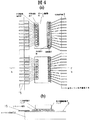
図5は、ゲート回路基板15を介してゲート駆動回路5に入力される各信号(換言すれば、コントロール回路12から出力される各信号)と、各ゲート駆動回路5から各走査信号線3に供給される信号との関係を示している。
【0043】
〔ドレイン駆動回路周辺の構成〕
図6は、ドレイン駆動回路およびその周辺の構成の詳細を示す図で、同図(a)は平面図で図1の点線で囲まれた枠Qの部分を示し、同図(b)は同図(a)のb−b線における断面図である。
同図から明らかとなるように、ゲート駆動回路5の周辺の構成とほぼ同じになっている。
ここで、ゲート駆動回路5の周辺の構成と異なる部分は、図1の構成で説明したように、図中x方向に並設されている各ドレイン駆動回路6のうち左半分の各ドレイン駆動回路6はドレイン回路基板16Aの側から信号が供給されるようになっており、右半分の各ドレイン駆動回路6はドレイン回路基板16Bの側から信号が供給されるようになっていることにある。
図7は、たとえば一方のドレイン回路基板16Aを介してドレイン駆動回路6に入力される各信号(換言すれば、コントロール回路12から出力される各信号)と、各ドレイン駆動回路6から各映像信号線4に供給される信号との関係を示している。
なお、図6はドレイン駆動回路6がx方向に並設されている状態で示しているのに対し、図7はドレイン駆動回路6がy方向に並設されている状態で示している。
【0044】
〔フレキシブル配線基板〕
図8は、ゲート回路基板15、ドレイン回路基板16A、およびドレイン回路基板16Bの断面を示している。
同図から明らかなように、これら各回路基板15,16A,16Bは多層構造からなっている。
すなわち、各層は、ポリイミドフィルム60を基板としてCuからなる配線層61が形成され、その表面にはCuメッキ62がなされている。そして、これら各層は接着材63によって接着されることによって多層となっている。
そして、各層の配線層との接続は、それら配線層の重畳部において形成された貫通孔64に充填された導電材によってなされている。
この場合、液晶表示パネル1に接続される部分は、単層になっており、その端子にはAuメッキ65が施されている。
【0045】
他の実施例
上述した実施例では、ドレイン駆動回路6の側に接続される2個のドレイン回路基板16A,16Bに、コントロール回路12からの出力がそれぞれ入力されるように構成されたものである。
それによって、映像信号線への映像信号の波形歪みの発生を抑制せしめるためである。
しかし、該ドレイン回路基板16A,16Bの熱膨張による弊害を防止する目的のみならば、このように構成することなく、コントロール回路12からの出力をドレイン回路基板16Aに入力させ、さらに、このドレイン回路基板16Aを介してドレイン回路基板16Bに入力させるように構成してもよい。
すなわち、ドレイン回路基板16A,16Bはそれぞれ分割された形態をとるのみで、これら各ドレイン回路基板16A,16Bの信号伝達経路は従来と同様となる構成とするものである。
【0046】
上述した実施例では、ドレイン駆動回路6の側に接続される2個のドレイン回路基板16A,16Bは、コントロール基板10に接続されるそれぞれの接続部19A,19Bが、同じ方向(図中左側)に形成されたものである。
しかし、図9に示すように、ドレイン回路基板16A,16Bは、それら各接続部19A,19Bが互いに隣接するように配置するようにしてもよいことはいうまでもない。
そして、この場合、各接続部19A,19Bの間にコントロール回路12を配置させ、かつ、このコントロール回路12からの出力をそれぞれ前記各接続部19A,19Bを介してドレイン回路基板16A,16Bらに供給させることによって、該コントロール回路12から最も遠い位置にある映像信号線4までの距離を大幅に小さくさせることができるようになる。
このことは、該コントロール回路12から最も遠い位置にある映像信号線4およびその近傍の映像信号線4に供給される映像信号の波形歪みの発生を減少させることができるようになる。
【0047】
上述した各実施例では、ドレイン駆動回路6側のドレイン回路基板16A,16Bの改良について説明したものである。しかし、ゲート駆動回路5側のゲート回路基板15にも本発明を適用できることはいうまでもない。
ゲート駆動回路5側のゲート回路基板15は、ドレイン駆動回路6側のドレイン回路基板16A,16Bと比較して、供給される信号が異なるのみで、機械的構成においては全く同じである。そして、液晶表示パネル1の大型化がさらに進み、液晶表示パネル1のゲート駆動回路5側の辺がさらに大きくなることによって、同様の問題が発生するからである。
【0048】
上述した各実施例では、液晶表示装置としていわゆる横電界方式のものについて説明したものである。しかし、いわゆる縦電界方式のものについても適用できることはいうまでもない。
【0049】
ここで、縦電界方式の液晶表示装置とは、液晶を介して互いに対向配置される透明基板の液晶側の面に、それぞれ透明な電極が形成され、これら各電極の間の電位差によって液晶に電界を発生させる構造のものをいう。
このような液晶表示装置であっても、その液晶表示パネルに搭載される駆動回路、フレキシブル配線基板、およびプリント基板等において同じ構成ならば、そのまま本発明を適用できるからである。
【0050】
【発明の効果】
以上説明したことから明らかなように、本発明による液晶表示装置によれば、液晶表示パネルの大型化にも拘らず、該液晶表示パネルの透明基板に対するフレキシブル配線基板の接続不良を防止することができるようになる。
また、液晶表示パネルの大型化にも拘らず、並設される信号線の並設方向の一方の側の信号線における信号に波形の歪みが生じるのを防止することができるようになる。
【図面の簡単な説明】
【図1】本発明による液晶表示装置の一実施例を示す全体構成図である。
【図2】本発明による液晶表示装置のドレイン回路基板の他の実施例を示す構成図である。
【図3】本発明による液晶表示装置の画素の一実施例を示す平面図である。
【図4】本発明による液晶表示装置のゲート駆動回路およびその周辺の一実施例を示す構成図である。
【図5】本発明による液晶表示装置のゲート駆動回路の入出力信号の関係を示す図である。
【図6】本発明による液晶表示装置のドレイン駆動回路およびその周辺の一実施例を示す構成図である。
【図7】本発明による液晶表示装置のドレイン駆動回路の入出力信号の関係を示す図である。
【図8】本発明による液晶表示装置に用いられるフレキシブル基板の構成を示す断面図である。
【図9】本発明による液晶表示装置の他の実施例を示す説明図である。
【符号の説明】
1…液晶表示パネル、2…画素、5…ゲート駆動回路、6…ドレイン駆動回路、10…コントロール基板、12…コントロール回路、15…ゲート回路基板、16A,16B……ドレイン回路基板。[0001]
BACKGROUND OF THE INVENTION
The present invention relates to a liquid crystal display device, and more particularly to an active matrix liquid crystal display device.
[0002]
[Prior art]
The active matrix type liquid crystal display device is characterized in that a switching element made of, for example, a thin film transistor (TFT) is incorporated in each pixel of the liquid crystal display panel.
That is, each of the pixels formed in the spreading direction of the liquid crystal is arranged on the liquid crystal side surface of one of the transparent substrates. And a switching element which is configured by a portion surrounded by adjacent video signal lines and is driven by supply of a scanning signal from one scanning signal line, and a video signal which is supplied from one video signal line via this switching element Is applied to the pixel electrode.
Therefore, a signal from the scanning drive circuit is inputted from one end of each scanning signal line, and a signal from the video signal driving circuit is inputted from one end of each video signal line. Is entered. Each of these drive circuits is mounted on the periphery of one transparent substrate.
Each of these drive circuits is supplied with signals from, for example, a control circuit mounted on a printed circuit board, and the transmission of these signals is performed on the printed circuit board and one transparent substrate of the liquid crystal display panel. Some are performed by a flexible wiring board connected to (transparent substrate on which each drive circuit is mounted).
[0003]
[Problems to be solved by the invention]
However, it is pointed out that the liquid crystal display device configured in this way often causes a connection failure of the flexible wiring board to one transparent substrate of the liquid crystal display panel as it tends to be enlarged. It came to be done.
That is, one of the transparent substrates and the flexible wiring substrate is configured such that corresponding wiring terminals formed on the transparent substrate and the flexible wiring substrate are connected to each other. It was confirmed that it shifted from the wiring terminal on the transparent substrate side.
Since this deviation increases in proportion to the increase in the size of the liquid crystal display device (more precisely, the liquid crystal display panel), the countermeasure has become indispensable.
[0004]
Here, it has been found that the adverse effect of thermal expansion of the flexible wiring board occurs not only when the flexible wiring board is connected to one transparent substrate of the liquid crystal display panel, but also after the connection. Yes.
This is because even after the flexible wiring board is connected well, the connecting portion is peeled off due to the expansion of the flexible wiring board.
[0005]
Furthermore, the liquid crystal display device configured in this way is also adapted to the video signal on the video signal line on one side of the juxtaposed direction of the video signal lines arranged side by side as it tends to increase in size. It has been pointed out that waveform distortion tends to occur.
That is, the control circuit is configured to supply a signal to each drive circuit via the flexible wiring board, but the video signal transmitted to the video signal line far from the control circuit is transmitted. It was confirmed that waveform distortion was caused by the influence of other drive circuits connected in the process.
[0006]
The present invention has been made based on such circumstances, and the object thereof is a liquid crystal display capable of preventing poor connection of a flexible wiring board to a transparent substrate of the liquid crystal display panel, despite the increase in size of the liquid crystal display panel. To provide an apparatus.
In addition, an object of the present invention is to provide a liquid crystal display that can prevent waveform distortion from occurring in a signal in a signal line on one side of the juxtaposed direction of the signal lines arranged in parallel, despite the increase in size of the liquid crystal display panel. To provide an apparatus.
[0007]
[Means for Solving the Problems]
The means to solve the above problems are as follows.
<Means 1>
Liquid crystal,
A plurality of signal lines, a scanning signal line intersecting with the plurality of signal lines, a switching element driven by supply of a scanning signal from the scanning signal line, and a signal line connected to the signal line A first substrate having a pixel electrode;
A second substrate disposed opposite to the first substrate via the liquid crystal;
A printed circuit board on which a control circuit is mounted;
A first circuit board to which a signal from the control circuit is supplied;
A second circuit board to which a signal from the control circuit is supplied;
A plurality of drain drive circuits to which signals are supplied from the control circuit via the first circuit board or the second circuit board;
The first circuit board includes a first extension part partially extending toward the printed board, and the first extension part includes a first connection part connected to the printed board. ,
The second circuit board includes a second extension part partially extending toward the printed circuit board, and the second extension part includes a second connection part connected to the printed circuit board. ,
The first connection portion and the second connection portion are adjacent to each other;
The liquid crystal display device, wherein the control circuit is disposed between the first connection portion and the second connection portion.
<
Liquid crystal,
A plurality of signal lines, a scanning signal line intersecting with the plurality of signal lines, a switching element driven by supply of a scanning signal from the scanning signal line, and a signal line connected to the signal line A first substrate having a pixel electrode;
A second substrate disposed opposite to the first substrate via the liquid crystal;
A printed circuit board on which a control circuit is mounted;
A plurality of drain drive circuits arranged in parallel in the extending direction of the scanning signal lines and supplied with signals from a control circuit;
A first circuit board and a second circuit board;
The first circuit board includes a first extension part partially extending toward the printed board, and the first extension part includes a first connection part connected to the printed board. ,
The second circuit board includes a second extension part partially extending toward the printed circuit board, and the second extension part includes a second connection part connected to the printed circuit board. ,
When the plurality of drain drive circuits are divided into left and right halves with the extending direction of the scanning signal line as a horizontal direction,
A signal from the control circuit is supplied to the drain driving circuit of the left half through the first connection portion,
A signal from the control circuit is supplied to the right half drain drive circuit through the second connection portion,
The first connection portion and the second connection portion are adjacent to each other,
The liquid crystal display device, wherein the control circuit is disposed between the first connection portion and the second connection portion.
<
Liquid crystal,
A plurality of signal lines, a scanning signal line intersecting with the plurality of signal lines, a switching element driven by supply of a scanning signal from the scanning signal line, and a signal line connected to the signal line A first substrate having a pixel electrode;
A second substrate disposed opposite to the first substrate via the liquid crystal;
A printed circuit board on which a control circuit is mounted;
A plurality of drain drive circuits to which signals are supplied from the control circuit;
A plurality of drain drive circuits arranged in parallel in the extending direction of the scanning signal lines and supplied with signals from a control circuit;
A first circuit board;
A second circuit board,
The first circuit board includes a first extension part partially extending toward the printed board, and the first extension part includes a first connection part connected to the printed board. ,
The second circuit board includes a second extension part partially extending toward the printed circuit board, and the second extension part includes a second connection part connected to the printed circuit board. ,
A signal is supplied to the half of all drain drive circuits through the first connection, and a signal is supplied to the other half through the second connection.
The first connection portion and the second connection portion are adjacent to each other,
The liquid crystal display device, wherein the control circuit is disposed between the first connection portion and the second connection portion.
[0009]
DETAILED DESCRIPTION OF THE INVENTION
Hereinafter, embodiments of a liquid crystal display device according to the present invention will be described with reference to the drawings.
Example 1.
〔overall structure〕
FIG. 1 is a schematic configuration diagram showing an entire liquid crystal display device according to the present invention.
In this embodiment, the present invention is applied to a liquid crystal display device adopting a so-called lateral electric field method that is known to have a wide viewing angle.
[0010]
First, there is a liquid crystal display panel 1, and the liquid crystal display panel 1 includes transparent substrates 1 </ b> A and 1 </ b> B arranged opposite to each other via liquid crystal as an envelope. In this case, one transparent substrate (lower substrate in the figure: matrix substrate 1A) is formed slightly larger than the other transparent substrate (upper substrate in the figure: color filter substrate 1B), and the lower and right sides in the figure. The peripheral edges of the are almost flush with each other.
As a result, the periphery of the left side of the transparent substrate 1A in the drawing and the periphery of the upper side in the drawing are extended outward with respect to the other base transparent plate 1B. As will be described in detail later, this portion is a region where a gate drive circuit and a drain drive circuit are mounted.
[0011]
Here, as described above, each
[0012]
Each
In this case, a plurality of
Details of this part will be further described later with reference to FIG.
[0013]
Similarly, each video signal line 4 has one end (upper end in the figure) extending to the outside of the transparent substrate 1B and is connected to the output terminal of the drain drive circuit (IC) 6 mounted on the transparent substrate 1A. Connected.
Also in this case, a plurality of
Details of this portion will be further described later with reference to FIG.
[0014]
On the other hand, there is a printed circuit board 10 (control board 10) disposed in the vicinity of the liquid crystal display panel 1 on which the
The signal from the
[0015]
That is, on the
A part of the
[0016]
An output signal from the
[0017]
Also, on the
The
[0018]
An output signal from the
[0019]
Here, the feature of this embodiment is that the
The reason for this is to prevent adverse effects due to thermal expansion due to an increase in the length of the drain circuit substrate in the x direction in the drawing as the liquid crystal display panel 1 is enlarged.
[0020]
That is, if the drain circuit board is expanded by heat before the drain circuit board is connected to the liquid crystal display panel 1, sufficient electrical connection between the drain circuit board and the liquid crystal display panel 1 cannot be achieved.
Since the drain circuit board and the liquid crystal display panel 1 are provided with wiring terminals arranged so as to face each other, and these wiring terminals are connected through a conductor, a large thermal expansion is caused on the drain circuit board side. This is because when there is (compared to that of the transparent substrate), a shift occurs in each wiring terminal to be connected.
[0021]
Further, after the connection of the drain circuit board to the liquid crystal display panel 1, even if the above-mentioned problems are not caused and sufficient electrical connection is achieved, the drain circuit board is connected by the subsequent thermal expansion of the drain circuit board. This is because stress is generated between the wiring terminals, and the connection between them is peeled off.
[0022]
For this reason, by dividing the flexible wiring board into two as in this embodiment, the expansion of each of the
[0023]
From this, it goes without saying that the flexible wiring board is not necessarily limited to being divided into two. It is because the effect with respect to the evil mentioned above becomes still larger by making it more.
[0024]
Of course, the drain circuit board may be provided with means for reducing expansion due to heat at least on the side connected to the drive circuit.
[0025]
For example, as shown in FIG. 2, a
In this case, the drain circuit board is not divided as in the above-described embodiment, but it is possible to obtain the same effect as when the drain circuit board is divided.
[0026]
Further, as in the embodiment, for example, the
[0027]
The outputs from the
[0028]
In such a configuration, the distance from the connecting
That is, the capacity of the wiring of the
[0029]
As shown in FIG. 1, a video signal is supplied to the
[0030]
In this figure, the liquid crystal display panel 1, the
This is because the so-called frame area is reduced. Here, the frame means an area between the outline of the outer frame of the liquid crystal display device and the outline of the display unit. By reducing this area, the area of the display unit can be increased with respect to the outer frame. be able to.
[0031]
(Pixel configuration)
FIG. 3 is a plan view showing a detailed configuration of the
In the figure,
[0032]
That is, in this embodiment, the counter
By doing in this way, the counter
[0033]
In each pixel region, the counter
[0034]
Further, the main surface of the transparent substrate 1A on which the
[0035]
On the surface of this insulating film, first, a
[0036]
A
[0037]
Further, a
[0038]
Here, a portion of the
[0039]
The surface of the
[0040]
A protective film made of, for example, a silicon nitride film is formed on the upper surface of the insulating film on which the thin film transistor TFT, the
[0041]
Although not shown, a liquid crystal side portion of a transparent substrate (color filter substrate) 1B serving as a so-called upper substrate has a black matrix (indicated by
Further, a color filter is formed covering an opening formed in a portion corresponding to the pixel region of the
In addition, a flat film made of a resin film or the like is formed on the surface on which the black matrix and the color filter are formed, and an alignment film is formed on the surface of the flat film.
[0042]
[Configuration around the gate drive circuit]
4A and 4B are diagrams showing details of the configuration of the gate drive circuit and its periphery. FIG. 4A is a plan view showing a portion of a frame P surrounded by a dotted line in FIG. 1, and FIG. It is sectional drawing in the bb line of figure (a).
In the figure, a
These terminals are provided corresponding to the electrodes (bumps) on the output side of the
The
A wiring layer connected to each input electrode (bump) of the
The extending portion of the wiring layer is a portion connected to a terminal formed on the
As described above, a signal from the
FIG. 5 shows each signal input to the
[0043]
[Configuration around the drain drive circuit]
FIG. 6 is a diagram showing details of the configuration of the drain drive circuit and its periphery. FIG. 6 (a) is a plan view showing a portion of a frame Q surrounded by a dotted line in FIG. 1, and FIG. It is sectional drawing in the bb line of figure (a).
As is clear from the figure, the configuration around the
Here, the portions different from the peripheral configuration of the
FIG. 7 shows, for example, signals input to the
FIG. 6 shows the
[0044]
[Flexible wiring board]
FIG. 8 shows a cross section of the
As is clear from the figure, each of the
That is, each layer is formed with a
And the connection with the wiring layer of each layer is made | formed by the electrically conductive material with which the through-hole 64 formed in the overlapping part of those wiring layers was filled.
In this case, the portion connected to the liquid crystal display panel 1 is a single layer, and Au plating 65 is applied to its terminals.
[0045]
Other embodiments The above-described embodiments are configured such that the outputs from the
This is to suppress the occurrence of waveform distortion of the video signal to the video signal line.
However, if the purpose is only to prevent the harmful effects caused by the thermal expansion of the
In other words, the
[0046]
In the above-described embodiment, the two
However, as shown in FIG. 9, it goes without saying that the
In this case, the
This can reduce the occurrence of waveform distortion of the video signal supplied to the video signal line 4 located farthest from the
[0047]
In each of the above-described embodiments, the improvement of the
The
[0048]
In each of the embodiments described above, a so-called lateral electric field type liquid crystal display device has been described. However, it goes without saying that the present invention can also be applied to a so-called vertical electric field type.
[0049]
Here, the vertical electric field type liquid crystal display device is such that transparent electrodes are formed on the liquid crystal side surfaces of transparent substrates that are arranged to face each other via liquid crystal, and an electric field is applied to the liquid crystal by a potential difference between these electrodes. It has a structure that generates
This is because even in such a liquid crystal display device, the present invention can be applied as it is as long as it has the same configuration in a drive circuit, a flexible wiring board, a printed board, and the like mounted on the liquid crystal display panel.
[0050]
【The invention's effect】
As is apparent from the above description, according to the liquid crystal display device of the present invention, it is possible to prevent the connection failure of the flexible wiring board to the transparent substrate of the liquid crystal display panel, despite the increase in size of the liquid crystal display panel. become able to.
In addition, in spite of an increase in the size of the liquid crystal display panel, it is possible to prevent a waveform from being distorted in a signal in a signal line on one side of the parallel arrangement direction of the signal lines.
[Brief description of the drawings]
FIG. 1 is an overall configuration diagram showing an embodiment of a liquid crystal display device according to the present invention.
FIG. 2 is a block diagram showing another embodiment of the drain circuit board of the liquid crystal display device according to the present invention.
FIG. 3 is a plan view showing one embodiment of a pixel of a liquid crystal display device according to the present invention.
FIG. 4 is a block diagram showing an embodiment of a gate driving circuit of a liquid crystal display device according to the present invention and its periphery.
FIG. 5 is a diagram illustrating a relationship between input and output signals of a gate driving circuit of a liquid crystal display device according to the present invention.
FIG. 6 is a configuration diagram showing an embodiment of a drain driving circuit of a liquid crystal display device according to the present invention and its periphery.
FIG. 7 is a diagram illustrating a relationship between input and output signals of a drain driving circuit of a liquid crystal display device according to the present invention.
FIG. 8 is a cross-sectional view showing a configuration of a flexible substrate used in the liquid crystal display device according to the present invention.
FIG. 9 is an explanatory view showing another embodiment of the liquid crystal display device according to the present invention.
[Explanation of symbols]
DESCRIPTION OF SYMBOLS 1 ... Liquid crystal display panel, 2 ... Pixel, 5 ... Gate drive circuit, 6 ... Drain drive circuit, 10 ... Control board, 12 ... Control circuit, 15 ... Gate circuit board, 16A, 16B ... Drain circuit board.
Claims (3)
複数の信号線と、前記複数の信号線に交差する走査信号線と、前記走査信号線からの走査信号の供給によって駆動されるスイッチング素子と、前記スイッチング素子を介して信号線に接続されている画素電極と、を有する第1基板と、
前記液晶を介して第1基板に対して対向配置されている第2基板と、
コントロール回路が搭載されたプリント基板と、
前記コントロール回路からの信号が供給される第1の回路基板と、
前記コントロール回路からの信号が供給される第2の回路基板と、
前記第1の回路基板又は前記第2の回路基板を介して、前記コントロール回路から信号が供給される複数のドレイン駆動回路とを有し、
前記第1の回路基板は、前記プリント基板側に一部が延在した第1の延在部を備え、前記第1の延在部は前記プリント基板に接続された第1の接続部を備え、
前記第2の回路基板は、前記プリント基板側に一部が延在した第2の延在部を備え、前記第2の延在部は前記プリント基板に接続された第2の接続部を備え、
前記第1の接続部と前記第2の接続部とは互いに隣接し、
前記コントロール回路は、前記第1の接続部と前記第2の接続部との間に配置されていることを特徴とする液晶表示装置。Liquid crystal,
A plurality of signal Route, the scanning signal lines intersecting the plurality of signal Line, a switching element driven by a scan signal supplied from a scanning signal line is connected to signal Line via the switching element A first substrate having a pixel electrode;
A second substrate disposed opposite to the first substrate via the liquid crystal;
A printed circuit board on which a control circuit is mounted;
A first circuit board to which a signal from the control circuit is supplied;
A second circuit board to which a signal from the control circuit is supplied;
A plurality of drain drive circuits to which signals are supplied from the control circuit via the first circuit board or the second circuit board;
The first circuit board includes a first extension part partially extending toward the printed board, and the first extension part includes a first connection part connected to the printed board. ,
The second circuit board includes a second extension part partially extending toward the printed circuit board, and the second extension part includes a second connection part connected to the printed circuit board. ,
The first connection portion and the second connection portion are adjacent to each other;
The liquid crystal display device , wherein the control circuit is disposed between the first connection portion and the second connection portion .
複数の信号線と、前記複数の信号線に交差する走査信号線と、前記走査信号線からの走査信号の供給によって駆動されるスイッチング素子と、前記スイッチング素子を介して信号線に接続されている画素電極と、を有する第1基板と、
前記液晶を介して第1基板に対して対向配置されている第2基板と、
コントロール回路が搭載されたプリント基板と、
前記走査信号線の延在方向に並設され、コントロール回路から信号が供給される複数のドレイン駆動回路と、
第1の回路基板と第2の回路基板を有し、
前記第1の回路基板は、前記プリント基板側に一部が延在した第1の延在部を備え、前記第1の延在部は前記プリント基板に接続された第1の接続部を備え、
前記第2の回路基板は、前記プリント基板側に一部が延在した第2の延在部を備え、前記第2の延在部は前記プリント基板に接続された第2の接続部を備え、
前記走査信号線の延在方向を横として前記複数のドレイン駆動回路を左右半分に分けた場合、
左半分のドレイン駆動回路に対して、前記第1の接続部を介して前記コントロール回路からの信号を供給し、
右半分のドレイン駆動回路に対して、前記第2の接続部を介して前記コントロール回路からの信号を供給し、
前記第1の接続部と前記第2の接続部とは、互いに隣接し、
前記コントロール回路は、前記第1の接続部と前記第2の接続部との間に配置されていることを特徴とする液晶表示装置。Liquid crystal,
A plurality of signal Route, the scanning signal lines intersecting the plurality of signal lines, a switching element driven by a scan signal supplied from a scanning signal line is connected to signal Line via the switching element A first substrate having a pixel electrode;
A second substrate disposed opposite to the first substrate via the liquid crystal;
A printed circuit board on which a control circuit is mounted;
A plurality of drain drive circuits arranged in parallel in the extending direction of the scanning signal lines and supplied with signals from a control circuit;
A first circuit board and a second circuit board;
The first circuit board includes a first extending part partially extending toward the printed board, and the first extending part includes a first connecting part connected to the printed board. ,
The second circuit board includes a second extending part partially extending toward the printed board, and the second extending part includes a second connecting part connected to the printed board. ,
When the plurality of drain drive circuits are divided into left and right halves with the extending direction of the scanning signal line as a horizontal direction,
A signal from the control circuit is supplied to the left half drain drive circuit via the first connection portion,
A signal from the control circuit is supplied to the right half drain drive circuit via the second connection unit,
The first connection portion and the second connection portion are adjacent to each other,
The liquid crystal display device , wherein the control circuit is disposed between the first connection portion and the second connection portion .
複数の信号線と、前記複数の信号線に交差する走査信号線と、前記走査信号線からの走査信号の供給によって駆動されるスイッチング素子と、前記スイッチング素子を介して信号線に接続されている画素電極と、を有する第1基板と、
前記液晶を介して第1基板に対して対向配置されている第2基板と、
コントロール回路が搭載されたプリント基板と、
前記コントロール回路から信号が供給される複数のドレイン駆動回路と、
前記走査信号線の延在方向に並設され、コントロール回路から信号が供給される複数のドレイン駆動回路と、
第1の回路基板と、
第2の回路基板とを有し、
前記第1の回路基板は、前記プリント基板側に一部が延在した第1の延在部を備え、前記第1の延在部は前記プリント基板に接続された第1の接続部を備え、
前記第2の回路基板は、前記プリント基板側に一部が延在した第2の延在部を備え、前記第2の延在部は前記プリント基板に接続された第2の接続部を備え、
全ドレイン駆動回路の半数に対して前記第1の接続部を介して信号が供給され、もう半数に対して前記第2の接続部を介して信号が供給され、
前記第1の接続部と前記第2の接続部とは、互いに隣接し、
前記コントロール回路は、前記第1の接続部と前記第2の接続部との間に配置されていることを特徴とする液晶表示装置。Liquid crystal,
A plurality of signal Route, the scanning signal lines intersecting the plurality of signal Line, a switching element driven by a scan signal supplied from a scanning signal line is connected to signal Line via the switching element A first substrate having a pixel electrode;
A second substrate disposed opposite to the first substrate via the liquid crystal;
A printed circuit board on which a control circuit is mounted;
A drain drive circuit of several which device signals is supplied from the control circuit,
A plurality of drain drive circuits arranged in parallel in the extending direction of the scanning signal lines and supplied with signals from a control circuit;
A first circuit board;
A second circuit board,
The first circuit board includes a first extension part partially extending toward the printed board, and the first extension part includes a first connection part connected to the printed board. ,
The second circuit board includes a second extension part partially extending toward the printed circuit board, and the second extension part includes a second connection part connected to the printed circuit board. ,
A signal is supplied to the half of all drain drive circuits through the first connection, and a signal is supplied to the other half through the second connection.
The first connection portion and the second connection portion are adjacent to each other,
The liquid crystal display device , wherein the control circuit is disposed between the first connection portion and the second connection portion .
Priority Applications (7)
| Application Number | Priority Date | Filing Date | Title |
|---|---|---|---|
| JP34291698A JP3808224B2 (en) | 1998-12-02 | 1998-12-02 | Liquid crystal display |
| KR1019990054136A KR100314293B1 (en) | 1998-12-02 | 1999-12-01 | Liquid Crystal Display Device |
| TW088121012A TW539890B (en) | 1998-12-02 | 1999-12-01 | Liquid crystal display device |
| US09/452,462 US6583844B1 (en) | 1998-12-02 | 1999-12-02 | Liquid crystal display device |
| US11/165,554 USRE40706E1 (en) | 1998-12-02 | 2005-06-24 | Liquid crystal display device |
| US12/185,317 USRE41378E1 (en) | 1998-12-02 | 2008-08-04 | Liquid crystal display device |
| US12/814,805 USRE44314E1 (en) | 1998-12-02 | 2010-06-14 | Liquid crystal display device |
Applications Claiming Priority (1)
| Application Number | Priority Date | Filing Date | Title |
|---|---|---|---|
| JP34291698A JP3808224B2 (en) | 1998-12-02 | 1998-12-02 | Liquid crystal display |
Related Child Applications (1)
| Application Number | Title | Priority Date | Filing Date |
|---|---|---|---|
| JP2005334489A Division JP2006146225A (en) | 2005-11-18 | 2005-11-18 | Display apparatus |
Publications (3)
| Publication Number | Publication Date |
|---|---|
| JP2000171818A JP2000171818A (en) | 2000-06-23 |
| JP2000171818A5 JP2000171818A5 (en) | 2006-01-12 |
| JP3808224B2 true JP3808224B2 (en) | 2006-08-09 |
Family
ID=18357519
Family Applications (1)
| Application Number | Title | Priority Date | Filing Date |
|---|---|---|---|
| JP34291698A Expired - Lifetime JP3808224B2 (en) | 1998-12-02 | 1998-12-02 | Liquid crystal display |
Country Status (4)
| Country | Link |
|---|---|
| US (4) | US6583844B1 (en) |
| JP (1) | JP3808224B2 (en) |
| KR (1) | KR100314293B1 (en) |
| TW (1) | TW539890B (en) |
Families Citing this family (47)
| Publication number | Priority date | Publication date | Assignee | Title |
|---|---|---|---|---|
| JP3808224B2 (en) * | 1998-12-02 | 2006-08-09 | 株式会社 日立ディスプレイズ | Liquid crystal display |
| KR100666317B1 (en) * | 1999-12-15 | 2007-01-09 | 삼성전자주식회사 | Module for determing applied time of driving signal and liquid crystal display assembly having the same and method for driving liquid crystal display assembly |
| KR100385082B1 (en) | 2000-07-27 | 2003-05-22 | 삼성전자주식회사 | a liquid crystal display and a manufacturing method thereof |
| TW538395B (en) * | 2000-11-15 | 2003-06-21 | Toshiba Corp | Display device |
| JP4884586B2 (en) | 2000-12-18 | 2012-02-29 | 株式会社 日立ディスプレイズ | Liquid crystal display |
| JP3781967B2 (en) * | 2000-12-25 | 2006-06-07 | 株式会社日立製作所 | Display device |
| JP4485708B2 (en) * | 2001-05-21 | 2010-06-23 | シャープ株式会社 | Peripheral circuit board for liquid crystal display device and liquid crystal display device including the same |
| KR100755301B1 (en) * | 2001-06-25 | 2007-09-05 | 주식회사 엘지이아이 | A printed circuit board mounting structure of ceiling type air conditioner |
| JP2003108021A (en) * | 2001-09-28 | 2003-04-11 | Hitachi Ltd | Display device |
| JP3959253B2 (en) | 2001-10-02 | 2007-08-15 | 株式会社日立製作所 | Liquid crystal display device and portable display device |
| JP2003149665A (en) * | 2001-11-08 | 2003-05-21 | Hitachi Ltd | Liquid crystal display device |
| US7012667B2 (en) * | 2002-08-08 | 2006-03-14 | Hannstar Display Corp. | Liquid crystal display device |
| DE20213073U1 (en) * | 2002-08-26 | 2002-10-24 | Lee Ming Kuei | System-integrated reflective liquid crystal display device |
| JP3795445B2 (en) * | 2002-10-11 | 2006-07-12 | 株式会社 日立ディスプレイズ | Image display device |
| KR100891498B1 (en) * | 2002-11-04 | 2009-04-06 | 엘지디스플레이 주식회사 | Examination Apparatus for Liquid Crystal Panel |
| KR20040053950A (en) * | 2002-12-16 | 2004-06-25 | 엘지.필립스 엘시디 주식회사 | Manufacturing method for liquid crystal cell featuring cell scribing method |
| JP4217090B2 (en) * | 2003-03-20 | 2009-01-28 | 株式会社 日立ディスプレイズ | Display device |
| JP4004994B2 (en) * | 2003-06-05 | 2007-11-07 | 株式会社アドバンスト・ディスプレイ | Display device |
| KR100640212B1 (en) * | 2003-12-16 | 2006-10-31 | 엘지.필립스 엘시디 주식회사 | In plane switching mode liquid crystal display panel of strengthening connection of common electrode and method of fabricating thereof |
| JP3979405B2 (en) * | 2004-07-13 | 2007-09-19 | セイコーエプソン株式会社 | Electro-optical device, mounting structure, and electronic apparatus |
| JP4620534B2 (en) * | 2004-07-22 | 2011-01-26 | 三星電子株式会社 | Organic electroluminescent display |
| TW200638111A (en) * | 2005-04-19 | 2006-11-01 | Prime View Int Co Ltd | Active-matrix display panel |
| KR20060134730A (en) * | 2005-06-23 | 2006-12-28 | 삼성전자주식회사 | Array substrate and display device having the same |
| KR20070019401A (en) * | 2005-08-12 | 2007-02-15 | 삼성전자주식회사 | Drive film, drive package for organic light emitting diode display, method of manufacturing thereof anc organic light emitting diode display including the same |
| US8334960B2 (en) * | 2006-01-18 | 2012-12-18 | Samsung Display Co., Ltd. | Liquid crystal display having gate driver with multiple regions |
| KR20070095029A (en) * | 2006-03-20 | 2007-09-28 | 삼성전자주식회사 | Diplay device and method of manufacturing the same |
| KR101255275B1 (en) * | 2006-10-13 | 2013-04-15 | 엘지디스플레이 주식회사 | Steroscopic Liquid Crystal Display Device, method for Manufacturing the same and Bonding Apparatus for the same |
| JP2008191400A (en) * | 2007-02-05 | 2008-08-21 | Toshiba Matsushita Display Technology Co Ltd | Liquid crystal display device |
| US8350833B2 (en) * | 2007-04-06 | 2013-01-08 | Panasonic Corporation | Plasma display device |
| TWI446327B (en) * | 2007-04-17 | 2014-07-21 | Novatek Microelectronics Corp | Image processing method and related apparatus for a display device |
| KR101376044B1 (en) * | 2007-12-28 | 2014-04-02 | 삼성디스플레이 주식회사 | Display apparatus and method of driving therefor |
| TWI373107B (en) | 2008-04-24 | 2012-09-21 | Hannstar Display Corp | Chip having a driving integrated circuit and liquid crystal display having the same |
| CN102246218A (en) * | 2009-12-10 | 2011-11-16 | 松下电器产业株式会社 | Display panel module and display device |
| JP4660622B1 (en) * | 2009-12-14 | 2011-03-30 | 株式会社東芝 | Electronics |
| JP5452290B2 (en) * | 2010-03-05 | 2014-03-26 | ラピスセミコンダクタ株式会社 | Display panel |
| TWI476738B (en) * | 2010-09-07 | 2015-03-11 | Ind Tech Res Inst | Flexible display panel and assembly method thereof |
| CN102446926B (en) * | 2010-10-08 | 2014-09-03 | 财团法人工业技术研究院 | Flexible display panel and assembling method thereof |
| US8711570B2 (en) | 2011-06-21 | 2014-04-29 | Apple Inc. | Flexible circuit routing |
| KR20130029532A (en) * | 2011-09-15 | 2013-03-25 | 삼성전자주식회사 | Display device having functionality of radiating heat |
| JP6147533B2 (en) * | 2013-03-22 | 2017-06-14 | パナソニック液晶ディスプレイ株式会社 | Display device |
| KR20150080878A (en) * | 2014-01-02 | 2015-07-10 | 삼성전자주식회사 | Display module and display apparatus having the same |
| US10216302B2 (en) * | 2014-07-22 | 2019-02-26 | Synaptics Incorporated | Routing for an integrated display and input sensing device |
| KR102135232B1 (en) * | 2014-12-08 | 2020-07-20 | 삼성디스플레이 주식회사 | Curved display device and method of manufacturing the same |
| CN110554542B (en) * | 2018-05-30 | 2022-06-03 | 乐金显示有限公司 | Light control apparatus and transparent display device including the same |
| TWI666490B (en) * | 2018-06-15 | 2019-07-21 | 友達光電股份有限公司 | Electronic device |
| JP7309501B2 (en) * | 2019-07-19 | 2023-07-18 | 株式会社ジャパンディスプレイ | Electronics |
| US20230225051A1 (en) * | 2022-01-11 | 2023-07-13 | Himax Technologies Limited | Display system and a pad configuration adaptable thereto |
Family Cites Families (16)
| Publication number | Priority date | Publication date | Assignee | Title |
|---|---|---|---|---|
| US4904895A (en) | 1987-05-06 | 1990-02-27 | Canon Kabushiki Kaisha | Electron emission device |
| JP2865968B2 (en) | 1993-02-08 | 1999-03-08 | シャープ株式会社 | Panel mounting structure and mounting method |
| US5592199A (en) * | 1993-01-27 | 1997-01-07 | Sharp Kabushiki Kaisha | Assembly structure of a flat type device including a panel having electrode terminals disposed on a peripheral portion thereof and method for assembling the same |
| TW340192B (en) * | 1993-12-07 | 1998-09-11 | Sharp Kk | A display board having wiring with three-layered structure and a display device including the display board |
| TW344043B (en) * | 1994-10-21 | 1998-11-01 | Hitachi Ltd | Liquid crystal display device with reduced frame portion surrounding display area |
| US6081305A (en) * | 1995-05-30 | 2000-06-27 | Hitachi, Ltd. | Liquid crystal light valve and projection type liquid crystal display using such valve |
| JP3643640B2 (en) * | 1995-06-05 | 2005-04-27 | 株式会社東芝 | Display device and IC chip used therefor |
| JP3593392B2 (en) | 1995-09-27 | 2004-11-24 | 株式会社東芝 | Liquid crystal display |
| TW413993B (en) * | 1996-03-15 | 2000-12-01 | Sharp Kk | Image display device |
| JPH10197841A (en) | 1997-01-10 | 1998-07-31 | Mitsubishi Electric Corp | Liquid crystal display device |
| JP3658127B2 (en) | 1997-02-12 | 2005-06-08 | キヤノン株式会社 | Display device |
| JPH1152429A (en) * | 1997-06-05 | 1999-02-26 | Seiko Epson Corp | Substrate for liquid crystal panel, liquid crystal panel, and electronic equipment using the same |
| KR100269947B1 (en) * | 1997-09-13 | 2000-10-16 | 윤종용 | Printed circuit board and LCD module using it |
| US6266119B1 (en) * | 1998-01-13 | 2001-07-24 | Canon Kabushiki Kaisha | Liquid crystal apparatus and production process thereof |
| US6407795B1 (en) * | 1998-03-08 | 2002-06-18 | Matsushita Electric Industrial Co., Ltd. | Liquid crystal display and its inspecting method |
| JP3808224B2 (en) * | 1998-12-02 | 2006-08-09 | 株式会社 日立ディスプレイズ | Liquid crystal display |
-
1998
- 1998-12-02 JP JP34291698A patent/JP3808224B2/en not_active Expired - Lifetime
-
1999
- 1999-12-01 TW TW088121012A patent/TW539890B/en not_active IP Right Cessation
- 1999-12-01 KR KR1019990054136A patent/KR100314293B1/en active IP Right Grant
- 1999-12-02 US US09/452,462 patent/US6583844B1/en not_active Ceased
-
2005
- 2005-06-24 US US11/165,554 patent/USRE40706E1/en not_active Expired - Lifetime
-
2008
- 2008-08-04 US US12/185,317 patent/USRE41378E1/en not_active Expired - Lifetime
-
2010
- 2010-06-14 US US12/814,805 patent/USRE44314E1/en not_active Expired - Lifetime
Also Published As
| Publication number | Publication date |
|---|---|
| US6583844B1 (en) | 2003-06-24 |
| USRE44314E1 (en) | 2013-06-25 |
| USRE41378E1 (en) | 2010-06-15 |
| JP2000171818A (en) | 2000-06-23 |
| KR100314293B1 (en) | 2001-11-29 |
| USRE40706E1 (en) | 2009-05-05 |
| KR20000047824A (en) | 2000-07-25 |
| TW539890B (en) | 2003-07-01 |
Similar Documents
| Publication | Publication Date | Title |
|---|---|---|
| JP3808224B2 (en) | Liquid crystal display | |
| US6636288B2 (en) | Liquid crystal display | |
| JP3643640B2 (en) | Display device and IC chip used therefor | |
| JP3696512B2 (en) | Display element driving device and display device using the same | |
| KR100682403B1 (en) | Display device | |
| JP3730037B2 (en) | Liquid crystal display device | |
| US7088323B2 (en) | Liquid crystal display device and method for fabricating the same | |
| JP2000019556A (en) | Liquid crystal display device | |
| JP2002139741A (en) | Liquid crystal display device of equal resistance wiring | |
| JP2000019549A (en) | Liquid crystal display device | |
| KR19990012387A (en) | Structure of Tab Pad of LCD Panel and Manufacturing Method Thereof | |
| JP4975649B2 (en) | Display device | |
| JP2006146225A (en) | Display apparatus | |
| JPH10133232A (en) | Liquid crystal display device | |
| JPH11297760A (en) | Semiconductor chip, mounting structure thereof, and liquid crystal display | |
| KR100458839B1 (en) | Flat Panel Display | |
| JPH06202135A (en) | Liquid crystal display device | |
| JPH04281431A (en) | Liquid crystal display device | |
| JP2010212396A (en) | Electronic device, electro-optical device, and connection structure of substrate | |
| KR100825097B1 (en) | Liquid crystal display | |
| KR101032941B1 (en) | Thin film transistor array panel | |
| JP2004205550A (en) | Connecting electrode and picture display device | |
| WO2023216296A1 (en) | Driving circuit and display apparatus | |
| JPH04301622A (en) | Liquid crystal display device | |
| JP2000019550A (en) | Liquid crystal display device |
Legal Events
| Date | Code | Title | Description |
|---|---|---|---|
| A977 | Report on retrieval |
Free format text: JAPANESE INTERMEDIATE CODE: A971007 Effective date: 20050318 |
|
| A521 | Written amendment |
Free format text: JAPANESE INTERMEDIATE CODE: A523 Effective date: 20051118 |
|
| A871 | Explanation of circumstances concerning accelerated examination |
Free format text: JAPANESE INTERMEDIATE CODE: A871 Effective date: 20051118 |
|
| A975 | Report on accelerated examination |
Free format text: JAPANESE INTERMEDIATE CODE: A971005 Effective date: 20060203 |
|
| A131 | Notification of reasons for refusal |
Free format text: JAPANESE INTERMEDIATE CODE: A131 Effective date: 20060214 |
|
| A521 | Written amendment |
Free format text: JAPANESE INTERMEDIATE CODE: A523 Effective date: 20060417 |
|
| TRDD | Decision of grant or rejection written | ||
| A01 | Written decision to grant a patent or to grant a registration (utility model) |
Free format text: JAPANESE INTERMEDIATE CODE: A01 Effective date: 20060516 |
|
| A61 | First payment of annual fees (during grant procedure) |
Free format text: JAPANESE INTERMEDIATE CODE: A61 Effective date: 20060517 |
|
| R150 | Certificate of patent or registration of utility model |
Free format text: JAPANESE INTERMEDIATE CODE: R150 |
|
| FPAY | Renewal fee payment (event date is renewal date of database) |
Free format text: PAYMENT UNTIL: 20100526 Year of fee payment: 4 |
|
| FPAY | Renewal fee payment (event date is renewal date of database) |
Free format text: PAYMENT UNTIL: 20110526 Year of fee payment: 5 |
|
| S111 | Request for change of ownership or part of ownership |
Free format text: JAPANESE INTERMEDIATE CODE: R313115 Free format text: JAPANESE INTERMEDIATE CODE: R313121 |
|
| FPAY | Renewal fee payment (event date is renewal date of database) |
Free format text: PAYMENT UNTIL: 20110526 Year of fee payment: 5 |
|
| R350 | Written notification of registration of transfer |
Free format text: JAPANESE INTERMEDIATE CODE: R350 |
|
| FPAY | Renewal fee payment (event date is renewal date of database) |
Free format text: PAYMENT UNTIL: 20110526 Year of fee payment: 5 |
|
| FPAY | Renewal fee payment (event date is renewal date of database) |
Free format text: PAYMENT UNTIL: 20120526 Year of fee payment: 6 |
|
| FPAY | Renewal fee payment (event date is renewal date of database) |
Free format text: PAYMENT UNTIL: 20130526 Year of fee payment: 7 |
|
| FPAY | Renewal fee payment (event date is renewal date of database) |
Free format text: PAYMENT UNTIL: 20140526 Year of fee payment: 8 |
|
| R250 | Receipt of annual fees |
Free format text: JAPANESE INTERMEDIATE CODE: R250 |
|
| R250 | Receipt of annual fees |
Free format text: JAPANESE INTERMEDIATE CODE: R250 |
|
| R250 | Receipt of annual fees |
Free format text: JAPANESE INTERMEDIATE CODE: R250 |
|
| R250 | Receipt of annual fees |
Free format text: JAPANESE INTERMEDIATE CODE: R250 |
|
| R250 | Receipt of annual fees |
Free format text: JAPANESE INTERMEDIATE CODE: R250 |
|
| EXPY | Cancellation because of completion of term |