JP3773785B2 - Manufacturing method of semiconductor device - Google Patents
Manufacturing method of semiconductor device Download PDFInfo
- Publication number
- JP3773785B2 JP3773785B2 JP2000357156A JP2000357156A JP3773785B2 JP 3773785 B2 JP3773785 B2 JP 3773785B2 JP 2000357156 A JP2000357156 A JP 2000357156A JP 2000357156 A JP2000357156 A JP 2000357156A JP 3773785 B2 JP3773785 B2 JP 3773785B2
- Authority
- JP
- Japan
- Prior art keywords
- deposit
- etching
- oxide film
- trench
- film
- Prior art date
- Legal status (The legal status is an assumption and is not a legal conclusion. Google has not performed a legal analysis and makes no representation as to the accuracy of the status listed.)
- Expired - Fee Related
Links
Images


Landscapes
- Drying Of Semiconductors (AREA)
- Element Separation (AREA)
Description
【0001】
【発明の属する技術分野】
本発明は、半導体装置の製造方法に関し、特に、トレンチによる素子分離領域の形成方法に関する。
【0002】
【従来の技術】
近年、半導体装置の微細化が益々進み、例えば、1GBitDRAMでは、デザインルールが0.18μm以下となり、サブクォーターミクロンの加工を高精度に再現性良く行う技術が必要になってきている。半導体装置には素子を電気的に分離する素子分離領域が存在し、このようなサブクォーターミクロン領域の素子分離方としては、これまでの選択酸化法(LOCal Oxidation of Silicon:以下LOCOS法と称する)による素子分離領域の形成では困難である。
【0003】
そこで、LOCOS法に代わり、酸化物などの絶縁物質で埋め込まれたトレンチにより素子間を絶縁するトレンチ素子分離法(Shallow Trench Isolation:以下、STI法と称する)が盛んに研究されている。
【0004】
図11及び図12は、この種の従来のSTI法による素子分離領域の形成方法の一例を示す工程図である。
【0005】
まず、図11(a)に示すように、半導体基板、例えばシリコン基板101上
に第1のシリコン酸化膜(SiO2膜)102、シリコン窒化膜(Si3N4膜)103、第2のシリコン酸化膜(SiO2膜)104を順次積層形成する。その後、フォトリソグラフィー工程、ドライエッチング工程、レジスト剥離工程を用いて前記積層膜をパターニングして素子分離形成領域に開口部105aを有する積層膜パターン105を形成する。
【0006】
次に、図11(b)に示すように、前記積層膜パターン105をエッチングマスクとして、SiO2系の堆積付着物を生成しうるエッチングガスを使用した反応性イオンエッチング(RIE)法により、エッチング領域にSiO2系の堆積付着物106を付着させながら前記シリコン基板101をドライエッチングし、前記シリコン基板101上に素子分離のためのトレンチ107を形成する。このイオンエッチングは、一般に、HBrとCl2とO2のガス流量を約150、150、20 ml/min 、圧力を約2.7Pa、基板温度を60℃、RIE装置のRF出力を約500Wにより行われる。
【0007】
続いて、図11(c)に示すように、前記積層膜パターン105の第2のシリコン酸化膜104と前記SiO2系の堆積付着物106をHFを含んだ薬液を用いたウエットエチングにより除去した後、図11(d)に示すように、更に、前記シリコン窒化膜103をウェットエッチングにより横方向に後退させる。
【0008】
更に、図12(e)に示すように、前記トレンチ107側壁を熱酸化法により薄く酸化して酸化膜108を形成した後、図12(f)に示すように、前記トレンチ107内にシリコン酸化膜等の絶縁性物質109を埋め込む。この後、前記シリコン窒化膜103をストッパーとし、化学的・機械的研磨(CMP)を用いて前記絶縁性物質109を平坦化する。
【0009】
続いて、図12(g)に示すように、ウェットエッチングにより、前記絶縁性物質109を前記シリコン基板101の表面付近までエッチングした後、前記シリコン窒化103と前記第1のシリコン酸化膜102をウェットエッチングにより順次除去する。このようにして、シリコン基板101にSTI法による素子分離領域が形成される。
【0010】
【発明が解決しようとする課題】
しかしながら、上述したような従来の方法によれば、前記第2のシリコン酸化膜104と前記トレンチ107の側壁に付着された前記SiO2系の堆積付着物106との除去時に、HFを含んだ薬液を用いるため、図13(図11(c)のA部の拡大)に示すように、前記シリコン基板101を保護している前記第1のシリコン酸化膜102が横方向にエッチングされ、前記シリコン基板101表面が、直接、晒されるため、図14(図11(d)のB部の拡大)に示すように、前記シリコン窒化膜103を後退させた後、トレンチ107側壁を熱酸化法により薄く酸化する際に、半導体素子が形成される素子形成領域まで異常に酸化されてしまう問題がある。
【0011】
本発明は、トレンチ側壁を酸化する際に、素子形成領域を異常酸化することがない半導体装置の製造方法を提供することを目的とする。
【0012】
【課題を解決するための手段】
上記目的を達成するため、本発明の半導体装置の製造方法では、シリコン基板上に、シリコン酸化膜およびシリコン窒化膜を順次積層形成する第1の工程と、前記積層膜をパターニングして開口内に前記シリコン基板表面を露出させる第2の工程と、前記積層膜をマスクとして、前記シリコン基板表面を、エッチングガスとして該エッチング過程で前記マスク側壁を含む凹陥部にフロロカーボン系の堆積付着物を生成し得る第1のエッチングガ スを用いドライエッチングすることにより、当該シリコン基板表面に所定の深さを有する前記凹陥部を形成すると共に、前記マスクの前記シリコン酸化膜側壁に第1の堆積付着物を付着させる第3の工程と、前記積層膜をマスクとして、前記第1の堆積付着物表面に当該第1の堆積付着物と異質の第2の堆積付着物を付着させながら前記シリコン基板表面を、エッチングガスとして該エッチング過程でトレンチ側壁にSiO 2 系の堆積付着物を生成し得る第2のエッチングガスを用いドライエッチングすることにより、前記凹陥部の底部に、前記凹陥部に連なるトレンチを形成する第4の工程と、前記第2の堆積付着物を、ウエットエッチングにより除去する第5の工程と、前記第1の堆積付着物を、アッシングにより除去する第6の工程と、前記積層膜における前記シリコン窒化膜を横方向に後退させる第7の工程と、前記凹陥部および前記トレンチ内表面に、熱酸化により酸化膜を形成する第8の工程と、前記凹陥部および前記トレンチ内に絶縁性物質を埋め込み、素子分離領域を形成する第9の工程とを具備することを特徴とする。
【0013】
上記本発明によれば、SiO 2 系の第2の堆積付着物を除去する時にHFを含んだ薬液を用いても、シリコン基板を保護しているシリコン酸化膜は、フロロカーボン系の第1の堆積付着物により保護されているために、シリコン酸化膜が横方向にエッチングされることを防ぐことができる。
【0014】
【発明の実施の形態】
以下、本発明の半導体装置の製造方法に係る実施の形態について図面を参照して説明する。なお、説明の便宜のため、図面中の各膜厚やトレンチ深さは必ずしも実際のサイズに比例していない。
【0015】
(第1の実施形態)
まず、図1乃至図5を用いて、本発明の第1の実施形態に係わる半導体装置の製造方法を説明する。
【0016】
まず、図1(a)に示すように、半導体基板、例えばシリコン基板1上に熱酸化法により厚さ6nm程度の第 1 のシリコン酸化膜 ( SiO 2 膜 ) 2を形成し、更に、前記第 1 のシリコン酸化膜2上に、CVD法により厚さ100nm程度のシリコン窒化膜 ( Si 3 N 4 膜 ) 3と、厚さ100nm程度の第2のシリコン酸化膜(SiO 2 膜)4を順次積層形成する。
【0017】
次に、前記シリコン基板1上にレジスト膜(図示せず)をコーティングし、露光・現像工程を用いて開口部を有するレジストパターンを形成する。その後、前記レジストパターンをエッチングマスクとし、RIE法により、前記第2のシリコン酸化膜4、前記シリコン窒化膜3、前記第 1 のシリコン酸化膜2を順次エッチングすることにより、前記シリコン基板1の素子分離形成領域を露出させるための開口部5aを有する、前記第 1 のシリコン酸化膜2、前記シリコン窒化膜3及び前記第2のシリコン酸化膜4の積層膜パターン5を形成した後、前記レジストパターンを剥離する。
【0018】
次に、前記積層膜パターン5をエッチングマスクとして、反応性イオンエッチング(RIE)法により、前記開口部5a内の前記シリコン基板1表面を所定深さまでドライエッチングすることにより、トレンチ6を形成する。
【0019】
ここでは、前記シリコン基板 1 上の前記第1のシリコン酸化膜2を保護するために、トレンチ6の側壁にフロロカーボン系の堆積付着物7を付着させる必要があるため、2段階に分けてドライエッチングを行う。
【0020】
まず、図1(b)に示すように、第1段階において、前記第1のシリコン酸化膜2の側壁を含むエッチング領域にフロロカーボン系の堆積付着物7が付着する条件にて前記シリ コン基板 1 をドライエッチングして所定の深さを有する凹陥部(第1のトレンチ)6aを形成する。この第1段階において、エッチングガスとしては、例えばCH 2 F 2 、C 4 F 8 を含んだガスを用いる。このガス系では、蒸気圧の低い堆積物7であるCHxFyを生成し、前記第1のシリコン酸化膜2を含む前記トレンチ6a側壁および底部に付着する。
【0021】
なお、この第 1 段階のエッチング条件は、例えばCH 2 F 2 、C 4 F 8 のガス流量を約50、10 ml/min 、圧力を約5.3 Pa 、基板温度を約20℃、RIE装置のRF出力を約1000 W とする。
【0022】
次に、図1(c)に示すように、エッチング条件を変えて、引き続き、第2段階の前記シリコン基板1のドライエッチングを行う。即ち、前記第1の堆積付着物7及び前記積層膜パターン5をマスクとし、前記第1のトレンチ6aの底部に、この第1のトレンチ6aと連なる所定の深さの第2のトレンチ6bを形成する。
【0023】
ここでは、エッチングガスとして、例えばHBrとCl 2 とO 2 の混合ガスを用いる。このガス系では一部のガスが被エッチング材であるシリコンと反応し、蒸気圧の低い第2の堆積付着物8であるSiBrxClyOzを生成する。このSiO 2 系の第2の堆積付着物8は、前記第1の堆積付着物7表面を含む第2のトレンチ 6 bの側壁に付着し、前記第1のシリコン酸化膜2の側壁部分においては、フロロカーボン系の前記第1の堆積付着物7とSiO 2 系の第2の堆積付着物8との積層構造になる。
なお、この第2段階のエッチング条件は、例えばHBrとCl 2 とO 2 のガス流量を約150、150、20 ml/min 、圧力を約2.7 Pa 、基板温度を約60℃、RIE装置のRF出力を約500 W とする。
【0024】
なお、第 1 段階のドライエッチングにおいて、エッチングガスとしてC 5 F 8 、CHF 3 などのCFを含有するガスを使用しても、フロロカーボン系の堆積物が堆積することで同様の効果が得られる。また、第2のエッチングでは、フッ素を含有するガスを用いてもよい。
【0025】
次いで、図1(d)に示すように、ウェットエッチングにより積層膜パターン5の前記第2のシリコン酸化膜 4 とSiO 2 系の前記第2の堆積付着物 7 を除去する。
【0026】
続いて、図2(e)に示すように、アッシング工程により、フロロカーボン系の前記第1の堆積付着物7を除去した後、ウェットエッチングにより前記シリコン窒化膜3を横方向に後退させる。
【0027】
次いで、図2(f)に示すように、熱酸化法により、前記トレンチ 6 の側壁を薄く酸化して酸化膜9を形成した後、図2(g)に示すように、前記トレンチ6内にシリコン酸化膜等の絶縁性物質10を埋め込み、前記シリコン窒化膜3をストッパーとし、科学・機械的研磨(CMP)法を用いて前記絶縁性物質10を平坦化する。
【0028】
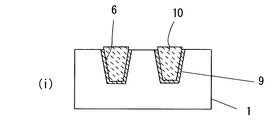
続いて、図2(h)に示すように、ウェットエッチングにより、前記絶縁性物質10を前記シリコン基板1の表面付近までエッチングした後、図3(i)に示すように、前記シリコン窒化膜3及び前記第1のシリコン酸化膜2をウエットエッチングにより、順次、除去する。このようにして、シリコン基板1にSTI法による素子分離領域を形成する。
【0029】
上記第1の実施形態によれば、前記第1のシリコン酸化膜2の側壁を保護するためのフロロカーボン系の第1の堆積付着物7上に、更にSiO 2 系の第2の堆積付着物8を積層付着させて、前記第1の堆積付着物7を前記第2の堆積付着物8で完全に被覆している。このため、図1(d)に示すように、前記積層膜パターン5の前記第2のシリコン酸化膜 4 とSiO 2 系の第2の堆積付着物8を除去する際に、前記第1のシリコン酸化膜2の側壁は、図4(図1(d)のc部の拡大)に示すように、フロロカーボン系の第1の堆積付着物7で保護されており、前記第1のシリコン酸化膜2は、横方向にエッチングされることがない。
【0030】
したがって、図5(図2(e)のd部分の拡大)に示すように、前記シリコン窒化膜3を横方向に後退させても、素子形成領域表面は前記第1のシリコン酸化膜2で保護されており、前記トレンチ側壁を熱酸化法により薄く酸化する際に、半導体素子が形成される素子形成領域まで食込んで酸化されることがなく、素子形成領域を精度良く画定することができる。
【0031】
(第2の実施形態)
次に、図6乃至図10を用いて本発明の第2の実施形態に係わる半導体装置の製造方法について説明する。
【0032】
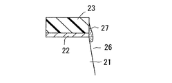
まず、図6(a)に示すように、シリコン基板21に熱酸化法により厚さ6nm程度の第 1 のシリコン酸化膜 ( SiO 2 膜 ) 22を形成し、更に、前記第1のシリコン酸化膜22上に、CVD法により厚さ100nm程度のシリコン酸化膜 ( Si 3 N 4 膜 ) 23と、厚さ100nm程度の第2のシリコン酸化膜 ( SiO 2 膜 ) 24を順次積層形成する。
【0033】
次に、前記シリコン基板21上にレジスト膜(図示せず)をコーティングし、露光・現像工程を用いて開口部を有するレジストパターンを形成する。その後、前記レジストパターンをエッチングマスクとし、RIE法により、前記第2のシリコン酸化膜24、前記シリコン窒化膜23、前記シリコン酸化膜22を順次エッチングすることにより、前記シリコン基板21の素子分離形成領域を露出するための開口部25aを有する、前記第1のシリコン酸化膜22、前記シリコン窒化膜23及び第2のシリコン酸化膜24の積層膜パターン25を形成した後、前記レジストパターンを剥離する。
【0034】
次に、前記積層膜パターン25をエッチングマスクとして、RIE法により所定の深さまでドライエッチングしていく。従来は連続する一条件でトレンチ26を所定の深さまでエッチングしていたが、本発明では、前記シリコン基板21上に形成した前記第1のシリコン酸化膜22を保護するために、トレンチ26の側壁に、フロロカーボン系の堆積付着物27を付着させる必要があるため、3段階に分けてドライエッチングを行う。
【0035】
まず、図6(b)に示すように、第1段階において、前記第1のシリコン酸化膜22を含むエッチング領域にフロロカーボン系の第1の堆積付着物27を付着する条件にて前記シリコン基板21をドライエッチングして所定の深さを有する凹陥部(第1のトレンチ)26aを形成する。この第1段階において、エッチングガスとしては、例えばCH 2 F 2 、C 4 F 8 を含んだガスを用いる。このガス系では、蒸気圧の低い第1の堆積物27であるCHxFyを生成し、前記第1のシリコン酸化膜22を含む前記第1のトレンチ26aの側壁および低部に付着する。
【0036】
なお、この第 1 段階のエッチング条件は、例えばCH 2 F 2 、C 4 F 8 のガス流量を約50、10 ml/min 、圧力を約5.3 Pa 、基板温度を約20℃、RIE装置のRF出力を約1000 W とする。
【0037】
次に第2段階として、図6(c)に示すように、エッチング条件を変えて、前記第1のトレンチ26a底部に付着したフロロカーボン系の前記第1の堆積付着物27のエッチングを行う。ここでは、エッチングガスとして、例えばO 2 を含有したガスを用いる。
【0038】
なお、この第2段階のエッチング条件は、例えばO 2 のガス流量を約100 ml/min 、圧力を約10.1 Pa 、基板温度を60℃、RIE装置のRF出力を約100 W とする。
【0039】
次に図6(d)に示すように、エッチング条件を変えて、引き続き、第3段階の前記シリコン基板21のドライエッチングを行う。即ち、前記第1のトレンチ26aの底部に、この第1のトレンチ26aと連なる所定の深さの第2のトレンチ26bを形成する。
【0040】
ここでは、エッチングガスとして、例えばHBrとCl 2 とO 2 の混合ガスを用いる。このガス系では一部のガスが被エッチング材であるシリコンと反応し、蒸気圧の低い第2の堆積物28であるSiBrxClyOzを生成する。このSiO 2 系の第2の堆積付着物28は、前記第 1 のシリコン酸化膜22を含む第2のトレンチ26bの側壁に付着し、前記第1のシリコン酸化膜22の側壁部分においては、フロロカーボン系の前記第1の堆積付着物27とSiO 2 系の第2の堆積付着物28との積層構造になる。
【0041】
なお、この第3段階のエッチング条件は、例えばHBrとCl 2 とO 2 のガス流量を約150、20、5 ml/min 、圧力を約2.7 Pa 、基板温度を約60℃、RIE装置のRF出力を約500 W とする。
【0042】
なお、第 1 段階のエッチングにおいて、エッチングガスとしてC 5 F 8 、CHF 3 などのCFを含有するガスを使用しても、フロロカーボン系の堆積物が堆積することで同様の効果が得られる。また、第3のエッチングでは、フッ素を含有するガスを用いてもよい。
【0043】
次いで、図7(e)に示すように、ウェットエッチングにより積層膜パターン25の前記第2のシリコン酸化膜24とSiO 2 系の前記第2の堆積付着物28を除去する。
【0044】
続いて、図7(f)に示すように、アッシング工程により、フロロカーボン系の前記第1の堆積付着物27を除去した後、ウェットエッチングにより前記シリコン窒化膜23を横方向に後退させる。
【0045】
次いで、図7(g)に示すように、熱酸化法により、前記トレンチ2 6 の側壁
を薄く酸化して酸化膜29を形成した後、図7(h)に示すように、前記トレンチ26内にシリコン酸化膜等の絶縁性物質30を埋め込み、前記シリコン窒化膜23をストッパーとし、化学・機械的研磨(CMP)法を用いて前記絶縁性物質30を平坦化する。
【0046】
続いて、図8(i)に示すように、ウェットエッチングにより、前記絶縁性物質30を前記シリコン基板21の表面付近までエッチングした後、図8(j)に示すように、前記シリコン窒化膜23及び前記第1のシリコン酸化膜22をウエットエッチングにより、順次、除去する。このようにして、シリコン基板21にSTI法による素子分離領域を形成する。
【0047】
上記第2の実施形態によれば、前記第1のシリコン酸化膜22の側壁を保護するためのフロロカーボン系の第1の堆積付着物27上に、更にSiO 2 系の第2の堆積付着物28を積層付着させて、前記第1の堆積付着物27を前記第2の堆積付着物28で完全に被覆している。このため、図7(e)に示すように、前記積層膜パターン25の前記第2のシリコン酸化膜2 4 とSiO 2 系の第2の堆積付着物28を除去する際に、前記第1のシリコン酸化膜22の側壁は、図9(図7(e)のe部の拡大)に示すように、フロロカーボン系の第1の堆積付着物27で保護されており、前記第1のシリコン酸化膜22は、横方向にエッチングされることがない。
【0048】
したがって、図10(図7(f)のf部分の拡大)に示すように、前記シリコン窒化膜 23を横方向に後退させても、素子形成領域表面は前記第1のシリコン酸化膜22で保護されており、前記トレンチ側壁を熱酸化法により薄く酸化する際に、半導体素子が形成される素子形成領域まで食込んで酸化されることがなく、素子形成領域を精度良く画定することができる。
【0049】
なお、本発明は、上記実施形態に限定されるものではなく、発明の要旨を逸脱しない範囲で、種々変形して実施できることは明らかである。
【0050】
【発明の効果】
以上の説明から明らかなように、本発明の半導体装置の製造方法によれば、シリコン基板表面に形成されたシリコン酸化膜の側壁を保護するためのフロロカーボン系の第1の堆積付着物上に、更にSiO 2 系の第2の堆積付着物を積層付着させて、前記第1の堆積付着物を第2の堆積付着物で完全に被覆している。このため、エッチングマスクとなるシリコン酸化膜とトレンチ側壁のSiO 2 系の第2の堆積付着物を除去する際にHFを含んだ薬液を用いても、シリコン基板を保護しているシリコン酸化膜の側壁は、フロロカーボン系の第1の堆積付着物により保護されており、該シリコン酸化膜は、横方向にエッチングされることがなく、トレンチ側壁を酸化する際に、素子形成領域まで食込んで酸化されることがなく、素子形成領域を精度良く確定できる。
【図面の簡単な説明】
【図1】 本発明の第1の実施の形態に係わる半導体装置の製造方法を説明するための工程断面図。
【図2】 本発明の第1の実施の形態に係わる半導体装置の製造方法を説明するための工程断面図。
【図3】 本発明の第1の実施の形態に係わる半導体装置の製造方法を説明するための工程断面図。
【図4】 図1(d)におけるc部分を拡大して示す拡大断面図。
【図5】 図2(e)におけるd部分を拡大して示す拡大断面図。
【図6】 本発明の第2の実施の形態に係わる半導体装置の製造方法を説明するための工程断面図。
【図7】 本発明の第2の実施の形態に係わる半導体装置の製造方法を説明するための工程断面図。
【図8】 本発明の第2の実施の形態に係わる半導体装置の製造方法を説明するための工程断面図。
【図9】 図7(e)におけるe部分を拡大して示す拡大断面図。
【図10】 図7(f)におけるf部分を拡大して示す拡大断面図。
【図11】 従来の半導体装置の製造方法を説明するための工程断面図。
【図12】 従来の半導体装置の製造方法を説明するための工程断面図。
【図13】 図11(a)におけるe部分を拡大して示す拡大断面図。
【図14】 図11(b)におけるf部分を拡大して示す拡大断面図。
【符号の説明】
1、21、101…シリコン基板( 半導体基板)
2、22、102…第1のシリコン酸化膜
3、23、103…シリコン窒化膜
4、24、104…第2のシリコン酸化膜
5、25、105…積層膜パターン
5a、25a、105a…開口部
6、26、107…トレンチ
6a、26a…凹陥部(第1のトレンチ)
6b、26b…第2のトレンチ
7、27…第1の堆積付着物(フロロカーボン系の堆積付着物)
8、28…第2の堆積付着物(SiO 2 系の堆積付着物)
9、29、108…酸化膜
10、30、109…絶縁性物質
106…SiO 2 系の堆積付着物 [0001]
BACKGROUND OF THE INVENTION
The present invention relates to a method for manufacturing a semiconductor device, and more particularly to a method for forming an element isolation region by a trench.
[0002]
[Prior art]
In recent years, semiconductor devices have been increasingly miniaturized. For example, in a 1 GBit DRAM, the design rule is 0.18 μm or less, and a technique for performing sub-quarter micron processing with high reproducibility is required. In a semiconductor device, there is an element isolation region for electrically isolating elements. As such an element isolation method in the sub-quarter micron region, a conventional selective oxidation method (LOCal Oxidation of Silicon: hereinafter referred to as a LOCOS method). It is difficult to form an element isolation region by the above.
[0003]
Therefore, in place of the LOCOS method, a trench element isolation method (Shallow Trench Isolation: hereinafter referred to as STI method) in which elements are insulated by a trench embedded with an insulating material such as an oxide has been actively studied.
[0004]
11 and 12 are process diagrams showing an example of a method for forming an element isolation region by this type of conventional STI method.
[0005]
First, as shown in FIG. 11A, a first silicon oxide film (SiO 2 film) 102, a silicon nitride film (Si 3 N 4 film) 103, and a second silicon are formed on a semiconductor substrate, for example, a
[0006]
Next, as shown in FIG. 11B, etching is performed by a reactive ion etching (RIE) method using an etching gas capable of generating a SiO 2 -based deposit using the laminated
[0007]
Subsequently, as shown in FIG. 11C, the second
[0008]
Further, as shown in FIG. 12E, the sidewall of the
[0009]
Subsequently, as shown in FIG. 12G, after the
[0010]
[Problems to be solved by the invention]
However, according to the conventional method as described above, a chemical solution containing HF is used when removing the second
[0011]
An object of the present invention is to provide a method of manufacturing a semiconductor device in which an element formation region is not abnormally oxidized when a trench side wall is oxidized.
[0012]
[Means for Solving the Problems]
In order to achieve the above object, in a method of manufacturing a semiconductor device according to the present invention, a first step of sequentially forming a silicon oxide film and a silicon nitride film on a silicon substrate, and patterning the stacked film into the opening A second step of exposing the surface of the silicon substrate; and using the laminated film as a mask, the silicon substrate surface is used as an etching gas to generate a fluorocarbon-based deposition deposit in the recessed portion including the mask side wall during the etching process. by dry etching using a first etching gas obtained, and forming the concave portion on the silicon substrate surface having a predetermined depth, the first deposits deposited on the silicon oxide film sidewalls of the mask A third step of attaching, and using the stacked film as a mask, the surface of the first deposition deposit is different from the first deposition deposit. The silicon substrate surface while the deposited deposition deposits of, by dry etching using the trench sidewalls in the etch process as the etching gas and the second etching gas capable of producing deposits of the deposited SiO 2 system, the recessed A fourth step of forming a trench connected to the recessed portion at the bottom of the part, a fifth step of removing the second deposited deposit by wet etching, and ashing the first deposited deposit. A sixth step of removing the silicon nitride film in the stacked film, a seventh step of retreating the silicon nitride film in the lateral direction, and an eighth step of forming an oxide film on the recessed portion and the inner surface of the trench by thermal oxidation. And a ninth step of embedding an insulating material in the recessed portion and the trench to form an element isolation region.
[0013]
According to the present invention, even when a chemical solution containing HF is used when removing the SiO 2 -based second deposition deposit, the silicon oxide film protecting the silicon substrate is the first fluorocarbon-based deposition. Since it is protected by the deposit, the silicon oxide film can be prevented from being etched in the lateral direction.
[0014]
DETAILED DESCRIPTION OF THE INVENTION
Embodiments of the method for manufacturing a semiconductor device according to the present invention will be described below with reference to the drawings. For convenience of explanation, each film thickness and trench depth in the drawings are not necessarily proportional to the actual size.
[0015]
(First embodiment)
First, a method for manufacturing a semiconductor device according to the first embodiment of the present invention will be described with reference to FIGS.
[0016]
First, as shown in FIG. 1 (a), a semiconductor substrate, for example, the first silicon oxide film (SiO 2 film) having a thickness of about 6nm by thermal oxidation on the
[0017]
Next, a resist film (not shown) is coated on the
[0018]
Next, the
[0019]
Here, in order to protect the first
[0020]
First, FIG. 1 (b), in a first step, the
[0021]
The first stage etching conditions are, for example, CH 2 F 2 and C 4 F 8 gas flow rates of about 50, 10 ml / min , pressure of about 5.3 Pa , substrate temperature of about 20 ° C., and RIE apparatus. and about 1000 W of RF output.
[0022]
Next, as shown in FIG. 1C, the etching conditions are changed, and then the second stage dry etching of the
[0023]
Here, for example, a mixed gas of HBr, Cl 2 and O 2 is used as the etching gas . In this gas system, a part of the gas reacts with silicon as the material to be etched to generate SiBrxClyOz as the second deposition deposit 8 having a low vapor pressure. The SiO 2 -based second deposition deposit 8 adheres to the side wall of the second trench 6 b including the surface of the
The second stage etching conditions are, for example, HBr, Cl 2 and O 2 gas flow rates of about 150, 150, 20 ml / min , pressure of about 2.7 Pa , substrate temperature of about 60 ° C., and RIE apparatus. and about 500 W of RF output.
[0024]
In the first- stage dry etching, even when a gas containing CF such as C 5 F 8 or CHF 3 is used as an etching gas, the same effect can be obtained by depositing a fluorocarbon deposit. In the second etching, a gas containing fluorine may be used.
[0025]
Next, as shown in FIG. 1D, the second
[0026]
Subsequently, as shown in FIG. 2E, after the fluorocarbon-based
[0027]
Next, as shown in FIG. 2 (f), the sidewall of the
[0028]
Subsequently, as shown in FIG. 2H, the insulating
[0029]
According to the first embodiment, the SiO 2 -based second deposition deposit 8 is further formed on the fluorocarbon-based
[0030]
Therefore, as shown in FIG. 5 (enlarged portion d in FIG. 2E), the surface of the element formation region is protected by the first
[0031]
(Second Embodiment)
Next, a method for manufacturing a semiconductor device according to the second embodiment of the present invention will be described with reference to FIGS.
[0032]
First, as shown in FIG. 6A, a first silicon oxide film ( SiO 2 film ) 22 having a thickness of about 6 nm is formed on a
[0033]
Next, a resist film (not shown) is coated on the
[0034]
Next, dry etching is performed to a predetermined depth by the RIE method using the
[0035]
First, as shown in FIG. 6B, in the first stage, the
[0036]
The first stage etching conditions are, for example, CH 2 F 2 and C 4 F 8 gas flow rates of about 50, 10 ml / min , pressure of about 5.3 Pa , substrate temperature of about 20 ° C., and RIE apparatus. and about 1000 W of RF output.
[0037]
Next, as a second step, as shown in FIG. 6C, the fluorocarbon-based
[0038]
The etching conditions in this second stage, for example, a gas flow rate of about 100 ml / min of O 2, a pressure of about 10.1 Pa, 60 ° C. The substrate temperature is about 100 W of RF output RIE apparatus.
[0039]
Next, as shown in FIG. 6D, the etching conditions are changed, and then the
[0040]
Here, for example, a mixed gas of HBr, Cl 2 and O 2 is used as the etching gas . In this gas system, a part of the gas reacts with silicon as the material to be etched to generate SiBrxClyOz as the second deposit 28 having a low vapor pressure. The SiO 2 based second deposition deposits 28 are adhered to the side wall of second trench 26b including the first
[0041]
The third etching conditions are, for example, HBr, Cl 2 and O 2 gas flow rates of about 150, 20, 5 ml / min , pressure of about 2.7 Pa , substrate temperature of about 60 ° C., and RIE apparatus. and about 500 W of RF output.
[0042]
In the first- stage etching, even when a gas containing CF such as C 5 F 8 or CHF 3 is used as an etching gas, the same effect can be obtained by depositing a fluorocarbon deposit. In the third etching, a gas containing fluorine may be used.
[0043]
Next, as shown in FIG. 7E, the second
[0044]
Subsequently, as shown in FIG. 7F, after removing the fluorocarbon-based
[0045]
Next, as shown in FIG. 7G, the side walls of the
As shown in FIG. 7 (h), an insulating
[0046]
Subsequently, as shown in FIG. 8 (i), the insulating
[0047]
According to the second embodiment, the SiO 2 -based second deposition deposit 28 is further formed on the fluorocarbon-based
[0048]
Therefore, as shown in FIG. 10 (enlarged portion f in FIG. 7F), even if the
[0049]
It should be noted that the present invention is not limited to the above-described embodiment, and it is obvious that various modifications can be made without departing from the spirit of the invention.
[0050]
【The invention's effect】
As is apparent from the above description, according to the method for manufacturing a semiconductor device of the present invention, on the first fluorocarbon-based deposit for protecting the side wall of the silicon oxide film formed on the surface of the silicon substrate, Further, a second deposited deposit of SiO 2 is laminated and adhered, and the first deposited deposit is completely covered with the second deposited deposit. For this reason, the silicon oxide film that protects the silicon substrate even if a chemical solution containing HF is used to remove the SiO 2 -based second deposited deposit on the sidewall of the trench and the silicon oxide film serving as an etching mask . The side walls are protected by the first fluorocarbon-based deposits, and the silicon oxide film is not etched in the lateral direction. When the trench side walls are oxidized, the silicon oxide film digs into the element formation region and oxidizes. Therefore, the element formation region can be determined with high accuracy.
[Brief description of the drawings]
FIG. 1 is a process cross-sectional view for explaining a method for manufacturing a semiconductor device according to a first embodiment of the invention.
FIG. 2 is a process cross-sectional view for explaining the method for manufacturing the semiconductor device according to the first embodiment of the invention.
FIG. 3 is a process cross-sectional view for explaining the method for manufacturing the semiconductor device according to the first embodiment of the invention.
4 is an enlarged cross-sectional view showing an enlarged portion c in FIG . 1 (d).
FIG. 5 is an enlarged cross-sectional view showing a portion d in FIG.
FIG. 6 is a process sectional view for explaining the method for manufacturing the semiconductor device according to the second embodiment of the present invention.
FIG. 7 is a process sectional view for explaining the method for manufacturing the semiconductor device according to the second embodiment of the invention.
FIG. 8 is a process cross-sectional view for explaining the method for manufacturing the semiconductor device according to the second embodiment of the invention.
FIG. 9 is an enlarged cross-sectional view showing an e portion in FIG.
FIG. 10 is an enlarged cross-sectional view showing an f portion in FIG.
FIG. 11 is a process cross-sectional view for explaining a conventional method for manufacturing a semiconductor device.
FIG. 12 is a process cross-sectional view for explaining a conventional method for manufacturing a semiconductor device.
FIG. 13 is an enlarged cross-sectional view showing an e portion in FIG.
FIG. 14 is an enlarged cross-sectional view showing an f portion in FIG.
[Explanation of symbols]
1, 21, 101 ... silicon substrate ( Semiconductor substrate)
2, 22, 102 ... first silicon oxide film
3, 23, 103 ... silicon nitride film
4, 24, 104 ... second silicon oxide film
5, 25, 105 ... laminated film pattern
5a, 25a, 105a ... opening
6, 26, 107 ... trench
6a, 26a ... recessed portion (first trench)
6b, 26b ... second trench
7, 27 ... first deposit deposit (fluorocarbon-based deposit deposit)
8, 28 ... second deposit deposit (SiO 2 deposit deposit)
9, 29, 108 ... oxide film
10, 30, 109 ... insulating material
106 ... SiO 2 deposits
Claims (3)
前記積層膜をパターニングして開口内に前記シリコン基板表面を露出させる第2の工程と、A second step of patterning the laminated film to expose the surface of the silicon substrate in the opening;
前記積層膜をマスクとして、前記シリコン基板表面を、エッチングガスとして該エッチング過程で前記マスク側壁を含む凹陥部にフロロカーボン系の堆積付着物を生成し得る第1のエッチングガスを用いドライエッチングすることにより、当該シリコン基板表面に所定の深さを有する前記凹陥部を形成すると共に、前記マスクの前記シリコン酸化膜側壁に第1の堆積付着物を付着させる第3の工程と、By dry-etching the surface of the silicon substrate using the laminated film as a mask and using a first etching gas that can generate a fluorocarbon-based deposition deposit in the recessed portion including the mask sidewall in the etching process as an etching gas. A third step of forming the recessed portion having a predetermined depth on the surface of the silicon substrate and attaching a first deposition deposit to the side wall of the silicon oxide film of the mask;
前記積層膜をマスクとして、前記第1の堆積付着物表面に当該第1の堆積付着物と異質の第2の堆積付着物を付着させながら前記シリコン基板表面を、エッチングガスとして該エッチング過程でトレンチ側壁にSiOUsing the laminated film as a mask, the second deposition deposit different from the first deposition deposit is adhered to the surface of the first deposition deposit, while the silicon substrate surface is used as an etching gas to form a trench in the etching process. SiO on the side wall 22 系の堆積付着物を生成し得る第2のエッチングガスを用いドライエッチングすることにより、前記凹陥部の底部に、前記凹陥部に連なるトレンチを形成する第4の工程と、A fourth step of forming a trench connected to the recessed portion at the bottom of the recessed portion by dry etching using a second etching gas capable of generating a deposited deposit of the system;
前記第2の堆積付着物を、ウエットエッチングにより除去する第5の工程と、A fifth step of removing the second deposited deposit by wet etching;
前記第1の堆積付着物を、アッシングにより除去する第6の工程と、A sixth step of removing the first deposited deposit by ashing;
前記積層膜における前記シリコン窒化膜を横方向に後退させる第7の工程と、A seventh step of retracting the silicon nitride film in the laminated film in a lateral direction;
前記凹陥部および前記トレンチ内表面に、熱酸化により酸化膜を形成する第8の工程と、An eighth step of forming an oxide film by thermal oxidation on the recess and the inner surface of the trench;
前記凹陥部および前記トレンチ内に絶縁性物質を埋め込み、素子分離領域を形成する第9の工程とを具備することを特徴とする半導体装置の製造方法。And a ninth step of forming an element isolation region by embedding an insulating material in the recessed portion and the trench.
Priority Applications (1)
| Application Number | Priority Date | Filing Date | Title |
|---|---|---|---|
| JP2000357156A JP3773785B2 (en) | 2000-11-24 | 2000-11-24 | Manufacturing method of semiconductor device |
Applications Claiming Priority (1)
| Application Number | Priority Date | Filing Date | Title |
|---|---|---|---|
| JP2000357156A JP3773785B2 (en) | 2000-11-24 | 2000-11-24 | Manufacturing method of semiconductor device |
Publications (3)
| Publication Number | Publication Date |
|---|---|
| JP2002164426A JP2002164426A (en) | 2002-06-07 |
| JP2002164426A5 JP2002164426A5 (en) | 2005-02-17 |
| JP3773785B2 true JP3773785B2 (en) | 2006-05-10 |
Family
ID=18829266
Family Applications (1)
| Application Number | Title | Priority Date | Filing Date |
|---|---|---|---|
| JP2000357156A Expired - Fee Related JP3773785B2 (en) | 2000-11-24 | 2000-11-24 | Manufacturing method of semiconductor device |
Country Status (1)
| Country | Link |
|---|---|
| JP (1) | JP3773785B2 (en) |
Families Citing this family (6)
| Publication number | Priority date | Publication date | Assignee | Title |
|---|---|---|---|---|
| JP5319868B2 (en) * | 2005-10-17 | 2013-10-16 | ルネサスエレクトロニクス株式会社 | Manufacturing method of semiconductor device |
| JP2007142258A (en) * | 2005-11-21 | 2007-06-07 | Matsushita Electric Ind Co Ltd | Manufacturing method of semiconductor device |
| JP5091452B2 (en) * | 2006-10-06 | 2012-12-05 | 株式会社東芝 | Manufacturing method of semiconductor device |
| JP2008108923A (en) * | 2006-10-26 | 2008-05-08 | Elpida Memory Inc | Semiconductor device and its manufacturing method |
| JP2008227360A (en) * | 2007-03-15 | 2008-09-25 | Elpida Memory Inc | Method for manufacturing semiconductor device |
| CN105719965A (en) * | 2014-12-04 | 2016-06-29 | 北京北方微电子基地设备工艺研究中心有限责任公司 | Method and device for etching silicon dioxide substrate |
-
2000
- 2000-11-24 JP JP2000357156A patent/JP3773785B2/en not_active Expired - Fee Related
Also Published As
| Publication number | Publication date |
|---|---|
| JP2002164426A (en) | 2002-06-07 |
Similar Documents
| Publication | Publication Date | Title |
|---|---|---|
| US6784077B1 (en) | Shallow trench isolation process | |
| US6159822A (en) | Self-planarized shallow trench isolation | |
| JPH01290236A (en) | Method of levelling wide trench | |
| US6475875B1 (en) | Shallow trench isolation elevation uniformity via insertion of a polysilicon etch layer | |
| US6171929B1 (en) | Shallow trench isolator via non-critical chemical mechanical polishing | |
| JP4139380B2 (en) | Method for forming an isolation film in a semiconductor device | |
| US20100129983A1 (en) | Method of Fabricating Semiconductor Device | |
| US20040018695A1 (en) | Methods of forming trench isolation within a semiconductor substrate | |
| JP3773785B2 (en) | Manufacturing method of semiconductor device | |
| US6617223B2 (en) | Semiconductor-on-insulator structure fabrication having a temporary plug | |
| KR100677998B1 (en) | Method for manufacturing shallow trench isolation layer of the semiconductor device | |
| US6022789A (en) | Method of selective oxidation | |
| KR100442852B1 (en) | Method for forming trench isolation region to embody isolation region proper for high integrated semiconductor device | |
| US7045434B2 (en) | Semiconductor device and method for manufacturing the same | |
| US5880005A (en) | Method for forming a tapered profile insulator shape | |
| GB2333644A (en) | A method of forming void free trench isolation | |
| US7214595B2 (en) | Method of producing semiconductor devices | |
| US6281063B1 (en) | Method for manufacturing trench isolation | |
| KR100237749B1 (en) | Method of forming a device isolation film of semiconductor device | |
| KR100559553B1 (en) | Method for manufacturing shallow trench isolation layer of the semiconductor device | |
| KR100325626B1 (en) | Method for forming shallow trench isolation | |
| KR100935251B1 (en) | Method for manufacturing nano space of the semiconductor device | |
| US7067390B2 (en) | Method for forming isolation layer of semiconductor device | |
| KR100312983B1 (en) | A method for forming isolation layer in semiconductor device | |
| JP2000133711A (en) | Semiconductor device and its manufacture |
Legal Events
| Date | Code | Title | Description |
|---|---|---|---|
| A521 | Written amendment |
Free format text: JAPANESE INTERMEDIATE CODE: A523 Effective date: 20040310 |
|
| A621 | Written request for application examination |
Free format text: JAPANESE INTERMEDIATE CODE: A621 Effective date: 20040310 |
|
| A977 | Report on retrieval |
Free format text: JAPANESE INTERMEDIATE CODE: A971007 Effective date: 20041020 |
|
| A131 | Notification of reasons for refusal |
Free format text: JAPANESE INTERMEDIATE CODE: A131 Effective date: 20041029 |
|
| A521 | Written amendment |
Free format text: JAPANESE INTERMEDIATE CODE: A523 Effective date: 20041224 |
|
| RD02 | Notification of acceptance of power of attorney |
Free format text: JAPANESE INTERMEDIATE CODE: A7422 Effective date: 20050414 |
|
| RD04 | Notification of resignation of power of attorney |
Free format text: JAPANESE INTERMEDIATE CODE: A7424 Effective date: 20050606 |
|
| TRDD | Decision of grant or rejection written | ||
| A01 | Written decision to grant a patent or to grant a registration (utility model) |
Free format text: JAPANESE INTERMEDIATE CODE: A01 Effective date: 20060214 |
|
| A61 | First payment of annual fees (during grant procedure) |
Free format text: JAPANESE INTERMEDIATE CODE: A61 Effective date: 20060215 |
|
| FPAY | Renewal fee payment (event date is renewal date of database) |
Free format text: PAYMENT UNTIL: 20100224 Year of fee payment: 4 |
|
| FPAY | Renewal fee payment (event date is renewal date of database) |
Free format text: PAYMENT UNTIL: 20100224 Year of fee payment: 4 |
|
| FPAY | Renewal fee payment (event date is renewal date of database) |
Free format text: PAYMENT UNTIL: 20110224 Year of fee payment: 5 |
|
| LAPS | Cancellation because of no payment of annual fees |