JP3763263B2 - Receiver for spread spectrum communication - Google Patents
Receiver for spread spectrum communication Download PDFInfo
- Publication number
- JP3763263B2 JP3763263B2 JP2000377889A JP2000377889A JP3763263B2 JP 3763263 B2 JP3763263 B2 JP 3763263B2 JP 2000377889 A JP2000377889 A JP 2000377889A JP 2000377889 A JP2000377889 A JP 2000377889A JP 3763263 B2 JP3763263 B2 JP 3763263B2
- Authority
- JP
- Japan
- Prior art keywords
- data
- correlation value
- value data
- phase
- correlation
- Prior art date
- Legal status (The legal status is an assumption and is not a legal conclusion. Google has not performed a legal analysis and makes no representation as to the accuracy of the status listed.)
- Expired - Fee Related
Links
Images


Description
【0001】
【発明の属する技術分野】
本発明は、スペクトル拡散通信において使用される受信装置に係わり、特に、スペクトル拡散通信の受信信号と拡散符号との相関を表す相関値を算出する方法に係わる。
【0002】
【従来の技術】
無線通信システムのひとつとして、スペクトル拡散通信が知られている。スペクトル拡散通信では、データは、拡散符号を用いて拡散されて伝送される。そして、受信機は、送信機において使用された拡散符号と同じ符号を用いて受信信号を逆拡散することによりデータを再生する。なお、スペクトル拡散通信方法は、CDMA(Code Division Multiple Access )を実現する基盤技術である。
【0003】
図11は、スペクトル拡散通信の原理を説明する図である。なお、スペクトル拡散通信を実現する技術としては、直接拡散方式および周波数ホッピング方式が知られているが、以下では、直接拡散方式について説明する。
直接拡散方式では、送信装置において、伝送データに直接的に拡散符号が乗算される。拡散符号は、伝送データよりも高速のデータ列である。図11に示す例では、拡散符号は、11チップのデータ列"01010011101" である。この場合、伝送データが「1」であれば、そのビットの拡散信号は"01010011101" となり、伝送データが「0」であれば、そのビットの拡散信号は"10101100010" となる。そして、拡散符号は、搬送波に載せられて無線伝送路に送出される。
【0004】
受信装置は、送信装置において使用された拡散符号と同じ拡散符号を受信信号に乗算することにより伝送データを再生する。ここで、この乗算処理は、実質的には、受信信号と拡散符号との相関を検出する処理と同じである。そして、この相関値(受信信号の各チップの論理値と拡散符号の各チップの論理値とが一致する数)に基づいて、伝送データが再生される。図11に示す例では、「1」に拡散符号を乗算することによって得られた拡散信号"01010011101" に対して拡散符号を乗算することで"11111111111" が得られており、また、「0」に拡散符号を乗算することによって得られた拡散符号"10101100010" に対して拡散符号を乗算することで"00000000000" が得られている。そして、受信装置は、前者の乗算結果に対応する伝送データが「1」であると判断し、後者の乗算結果に対応する伝送データが「0」であると判断する。
【0005】
図12は、受信信号と拡散符号との相関を検出する方法を説明する図である。シフトレジスタ101は、拡散符号のチップ数と同じ段数であり、受信信号データ列を順番に格納する。拡散符号格納レジスタ102には、拡散符号が格納されている。乗算回路103は、シフトレジスタ101の段数と同じ数の排他的NOR回路を有し、シフトレジスタ101に新たなデータエレメントが入力される毎に、そのシフトレジスタ101に保持されているデータ列と拡散符号格納レジスタ102に格納されている拡散符号とを乗算する。そして、加算部104は、各排他的NOR回路の演算結果の和を相関値データとして出力する。なお、図2に示す回路は、デジタルマッチドフィルタまたは相関器と呼ばれている。
【0006】
このように、デジタルマッチドフィルタは、新たなデータエレメントが入力される毎に、順次、相関値データを出力していく。そして、受信装置は、この相関値データを利用して伝送データを再生するタイミングを検出し、さらに伝送データを再生する。
【0007】
なお、図12は、デジタルマッチドフィルタの基本構成を示しており、実際には、回路規模を小さくするために様々な形態が考案されている。例えば、特開平9−107271号公報、特開平11−274979号公報、特開2000−151361号公報には、乗算回路を使用することなく相関値データを生成する回路が提案されている。
【0008】
【発明が解決しようとする課題】
上記図11に示した例は、スペクトル拡散の原理を説明するための単純なモデルである。したがって、この場合は、相関値データから伝送データを再生することは比較的容易である。
【0009】
しかし、実際の通信システムでは、信号は、通常、変調されて伝送される。このため、受信装置において相関値データから伝送データを再生する処理は、図11を参照しながら説明したような簡単なものではない。例えば、QPSK変調を利用する通信システムでは、伝送データは、位相情報に変換されて伝搬される。この場合、伝送データは、位相平面上の信号点を利用して伝送される。即ち、送信装置は、伝送データを対応する信号点を表すI成分データおよびQ成分データに変換し、さらにそれらI成分データおよびQ成分データを拡散して送出する。一方、受信装置は、まず、I成分およびQ成分のそれぞれについて相関値データを生成し、続いて、それらの相関値データに基づいて位相を検出する。そして、その検出した位相から伝送データが再生される。
【0010】
このように、受信装置において相関値データから伝送データを再生する処理は簡単ではない。上述の例では、相関値データから位相を検出する際には、例えば大規模な変換テーブルが必要となることがある。しかたがって、データ再生処理を簡単にするためには、相関値データがデータ再生のために利用されやすいように修正または加工されていることが望ましい。
【0011】
本発明の課題は、スペクトル拡散通信において、受信信号と拡散符号との相関を表す相関値をデータ再生のために利用しやすいように修正または加工する方法を提供することである。
【0012】
【課題を解決するための手段】
本発明の受信装置は、スペクトル拡散通信において使用され、受信信号と拡散符号との相関を表す相関値データを生成するマッチドフィルタと、相関値データの取り得る範囲の中央値を表すデータ列の最上位ビットが1であり且つ他のビットが0となるように上記マッチドフィルタにより生成された相関値データを補正する補正手段と、上記補正手段により補正された相関値データに基づいて伝送データを再生する再生手段とを有する。
【0013】
上記補正手段により補正された相関値データの最上位ビットは、相関値データの符号または極性を表し、最上位ビット以外のビットは、相関値データの振幅を表す。これにより、相関値データの振幅がより少ないビット数で表されるので、同期検出処理およびデータ再生処理が簡単になる。
【0014】
本発明の受信装置は、上記構成において、上記補正手段が、補正後の相関値データが上記中央値以上であればその相関値データをそのまま出力し、補正後の相関値データが上記中央値よりも小さい場合には上記中央値を中心として上記補正後の相関値データの極性を反転させて出力し、上記再生手段が、上記補正手段の出力に基づいて伝送データを再生するようにしてもよい。
【0015】
この構成においては、補正手段から出力される相関値データが極性を持たないので、同期検出処理およびデータ再生処理がさらに簡単になる
【0016】
【発明の実施の形態】
図面を参照しながら、本発明の実施形態について説明する。なお、この実施例では、拡散方式として直接拡散方式が利用され、変調方式としてQPSK(4相PSK)が利用されるものとする。
【0017】
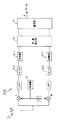
図1は、スペクトラム拡散通信システムにおいて使用される送信装置のブロック図である。送信装置は、伝送すべきデータを2ビットずつ符号化して無線網に送出する。すなわち、シリアル/パラレル変換器1は、伝送すべきデータを2ビットパラレルデータに変換する。符号化部2は、シリアル/パラレル変換器1から与えられる2ビットパラレルデータに対応する信号点の位相を表す情報を出力する。ここで、位相は、位相平面において互いに直交する成分の各振幅の組合せにより表すことができる。したがって、位相を表す情報は、例えば、位相平面上のコサイン成分を表す信号とサイン成分を表す信号である。以下では、これらの信号を、便宜上、それぞれIフェーズ信号およびQフェーズ信号と呼ぶことにする。
【0018】
拡散部3−1および3−2は、それぞれ符号化部2により生成されたIフェーズ信号およびQフェーズ信号を拡散する。具体的には、Iフェーズ信号およびQフェーズ信号に対して同一の拡散符号(例えば、バーカー系列)を乗積する。これにより、伝送すべき信号のスペクトルが拡散される。
【0019】
拡散部3−1により拡散されたIフェーズ信号及び3−2により拡散されたQフェーズ信号には、それぞれcos 波およびそれに直交するsin 波が乗積される。これらのcos 波およびsin 波は、発振器4により生成される。そして、これらの信号が合成されて無線網へ送出される。すなわち、搬送波は、拡散されたIフェーズ信号およびQフェーズ信号により変調されて出力される。
【0020】
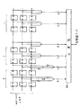
図2は、スペクトラム拡散通信システムにおいて使用される受信装置のブロック図である。受信装置は、無線網から受信した信号から2ビットデータを再生する。受信信号は、まず、互いに直交するcos 波およびsin 波が乗積される。これらのcos 波およびsin 波は、発振器4と同じ発振周波数を持った発振器11により生成される。これにより、受信信号の周波数がベースバンド付近のそれに変換される。なお、cos 波およびsin 波が乗積された受信信号を、それぞれ拡散Iフェーズ信号および拡散Qフェーズ信号と呼ぶことにする。ここで、拡散Iフェーズ信号および拡散Qフェーズ信号は、拡散復号されたときにそれぞれ受信信号の位相のコサイン成分及びサイン成分を表す信号であり、アナログデータである。したがって、1組の拡散Iフェーズ信号および拡散Qフェーズ信号は、拡散復号されたときに受信信号の位相を表すことになる。なお、「拡散復号」は、「逆拡散」または「再拡散」ともいう。
【0021】
拡散Iフェーズ信号および拡散Qフェーズ信号は、それぞれローパスフィルタにより高周波成分が除去された後、A/D変換器12−1および12−2に与えられる。A/D変換器12−1および12−2は、それぞれ拡散Iフェーズ信号及び拡散Qフェーズ信号としてのアナログデータをデジタルデータに変換する。このデジタルデータは、それぞれ複数ビット(例えば、3ビット)のデータである。
【0022】
相関部13−1および13−2は、それぞれA/D変換器12−1および12−2により生成されるデジタルデータと、送信装置において使用された拡散符号と同じ符号との相関をモニタし、その結果を同期検出部14に通知する。同期検出部14は、相関部13−1および13−2からの通知に基づいて同期タイミングを検出し、その同期タイミングにおいて相関部13−1および13−2により得られる1組の相関値データを差動復号部15に与える。この1組の相関値データは、受信信号の位相を表す。
【0023】
復号部15は、同期検出部14から与えられる1組の相関値データに対応したデータを生成する。なお、符号化部2および復号部15は、互いに対応する変換動作を行う。
このように、図1に示す送信装置および図2に示す受信装置を備えるスペクトラム拡散通信システムでは、伝送すべきデータは、QPSKを利用して2ビットずつ拡散されて伝送される。
【0024】
上記スペクトル拡散通信システムにおいて、本発明に特に係る技術は、相関部13−1および13−2において実現される。
図3は、相関部13のブロック図である。なお、「相関部13」は、互いに同じ構成である相関部13−1および13−2の総称である。
【0025】
相関部13は、デジタルマッチドフィルタ21および修正回路22を備える。デジタルマッチドフィルタ21は、入力系列と拡散符号との相関を表す相関値データを生成する。なお、相関値データを生成する処理は、入力系列に拡散符号を乗算してチップ毎の乗算結果の和を算出する処理と実質的に同じである。
【0026】
修正回路22は、デジタルマッチドフィルタ21により生成された相関値データを修正する。具体的には、修正回路22は、相関値データから振幅情報および位相情報を抽出する。そして、振幅情報は、修正された相関値データとして同期検出部14および復号部15に与えられる。また、位相情報は、復号部15に与えられる。
【0027】
次に、デジタルマッチドフィルタ21の構成および動作を説明する。デジタルマッチドフィルタ21は、既存の技術により実現可能であり、例えば、図12に示した構成であってもよいし、或いは、上述した公知文献(特開平9−107271号公報、特開平11−274979号公報、特開2000−151361号公報など)において提案されている構成であってもよい。ここでは、後者の構成を採り上げて説明する。
【0028】
図4は、デジタルマッチドフィルタの動作原理を説明するための図である。ここでは、11チップの拡散符号"01010011101" が使用されているものとする。また、A/D変換器においてオーバーサンプリングが行われてないものとする。
デジタルマッチドフィルタは、シフトレジスタ及び加算器を備える。ここで、シフトレジスタは、拡散符号のチップ数と同じ個数のフリップフロップ31a〜31kを直列に接続することにより構成される。なお、フリップフロップ31a〜31kは、それぞれ例えば、Dフリップフロップである。また、フリップフロップ31a〜31kは、拡散符号の各チップに対応して設けられている。たとえば、フリップフロップ31aは拡散符号の第1チップの「0」に対応しており、フリップフロップ31bは第2チップの「1」に対応している。
【0029】
加算器32は、フリップフロップ31a〜31kの各Q出力データの和を算出する。ただし、「1」に対応するフリップフロップのQ出力データがそのまま加算器32に与えられるのに対し、「0」に対応するフリップフロップのQ出力データは、反転回路によりその論理が反転された後に加算器32に与えられる。図4に示す例では、フリップフロップ31b、31d、31g〜31i、31kのQ出力データはそのまま加算器32に与えられる。一方、フリップフロップ31a、31c、31e、31f、31jのQ出力データは、反転回路によりその論理が反転された後に加算器32に与えられる。なお、加算器32の出力が相関値データである。
【0030】
上記構成のデジタルマッチドフィルタにおいて、受信信号データ列(A/D変換器12−1又は12−2の出力)は、シフトレジスタに入力される。そして、加算器32は、シフトレジスタに新たなデータエレメントが入力される毎に相関値を算出して出力する。
【0031】
また、上記構成において、「1」に対応するフリップフロップに「1」が書き込まれると、そのQ出力データは「1」になる。この時、加算器32には「1」が与えられる。一方、「0」に対応するフリップフロップに「0」が書き込まれると、そのQ出力データは「0」になる。しかし、「0」に対応するフリップフロップのQ出力には反転回路が設けられているので、この場合も、加算器32には「1」が与えられることになる。したがって、もし、「1」に対応する各フリップフロップにそれぞれ「1」が書き込まれ、「0」に対応する各フリップフロップにそれぞれ「0」が書き込まれると、加算器32には、11個の「1」が与えられることになる。この場合、加算器32は、「相関値データ=11」を出力する。
【0032】
反対に、もし、「1」に対応する各フリップフロップにそれぞれ「0」が書き込まれ、「0」に対応する各フリップフロップにそれぞれ「1」が書き込まれると、加算器32には、11個の「0」が与えられることになる。この場合、加算器32は、「相関値データ=0」を出力する。
【0033】
このように、図4に示すデジタルマッチドフィルタは、あるタイミングにおける受信信号データ列の各データエレメントと拡散符号の各チップの値とが一致した数を相関値データとして出力する。例えば、図4に示す構成では、受信信号データ列の各データエレメントと拡散符号の各チップの値とがすべて一致すると、「相関値データ=11」が出力され、すべて不一致であれば、「相関値データ=0」が出力される。
【0034】
図5は、図4に示すデジタルマッチドフィルタにより生成される相関値データの例である。相関値データは、基本的に、所定間隔ごとに極大値または極小値を持つ。ここで、これらの極大値または極小値が得られるタイミングは、同期タイミングであり、伝送データを再生するために使用される。例えば、最も単純なモデルでは、相関値データの極大値が得られるタイミング(T1 、T2 )において伝送データとして「1」が再生され、相関値データの極小値が得られるタイミング(T3 )において伝送データとして「0」が再生される。
【0035】
図6は、デジタルマッチドフィルタ21の具体的実施例でる。ここでは、A/D変換器12−1および12−2においてそれぞれ2倍オーバーサンプリングが行われるものとする。従って、拡散符号のチップ数が「11」であるので、デジタルマッチドフィルタ21のシフトレジスタの段数は「22」である。また、ここでは、A/D変換器12−1および12−2は、ぞれぞれ入力されたアナログデータを3ビットのデジタルデータに変換して出力するものとする。従って、デジタルマッチドフィルタ21には、3本のシフトレジスタが設けられている。そして、A/D変換器12−1または12−2から出力される3ビットのデジタルデータが、対応するシフトレジスタに入力される。なお、A/D変換器12−1および12−2の出力の取り得る範囲は、「000(10進数では0)」〜「111(10進数では7)」である。
【0036】
各シフトレジスタは、例えば、22個のフリップフロップを直列に接続することにより構成される。また、図4を参照しながら説明したように、「1」に対応するフリップフロップのQ出力データはそのまま加算器32に与えられ、「0」に対応するフリップフロップのQ出力データは、反転回路によりその論理が反転された後に加算器32に与えられる。
【0037】
上記構成において、例えば、「1」に対応するステージに「111(10進数では7)」が書き込まれると、即ち「1」に対応するステージの各フリップフロップにそれぞれ「1」が書き込まれると、各Q出力データはそれぞれ「1」になる。したがって、この場合、加算器32は、このステージから「111(10進数では7)」を受け取る。また、「1」に対応するステージに「000(10進数では0)」が書き込まれると、即ち「1」に対応するステージの各フリップフロップにそれぞれ「0」が書き込まれると、各Q出力データはそれぞれ「0」になる。したがって、この場合、加算器32は、このステージから「000(10進数では0)」を受け取る。
【0038】
一方、「0」に対応するステージに「111(10進数では7)」が書き込まれると、各フリップフロップのQ出力データは、それぞれ「1」になる。この場合、このステージの出力は「111」となる。ただし、「0」に対応するステージの出力には反転回路が設けられている。従って、この場合、加算器32は、このステージから「000(10進数では0)」を受け取る。また、「0」に対応するステージに「000(10進数では0)」が書き込まれると、各Q出力データはそれぞれ「0」になる。従って、この場合、加算器32は、このステージから「111(10進数では7)」を受け取る。
【0039】
このように、各ステージから加算器32に与えられる値は、「000(10進数では0)」〜「111(10進数では7)」の中の任意の値となる。ここで、シフトレジスタの段数は「22」である。したがって、加算器32により得られる加算結果の取り得る範囲は、「0」〜「154(=7×22)」である。すなわち、相関値データの取り得る範囲は、2進数で表すと、「00000000」〜「10011010」である。
【0040】
図7は、修正回路22の実施例である。修正回路22は、デジタルマッチドフィルタ21により生成された相関値データから振幅情報および位相情報を抽出する。
加算器41は、相関値データの取り得る範囲の中央値が所定の値になるようにデジタルマッチドフィルタ21の出力データに補正値を加算する。この実施例では、相関値データの取り得る範囲の中央値が「10000000」となるようにデジタルマッチドフィルタ21の出力データに「00110011」が加算されている。この結果、加算器41の出力データの取り得る範囲は、「00110011」〜「11001101」となる。
【0041】
検出部42は、加算器41の出力データの最上位ビットに基づいて、相関値データの極性(又は、符号)を検出する。具体的には、加算器41の出力データの最上位ビットが「1」であれば相関データの極性が「正」であるものと判断し、その最上位ビットが「0」であれば相関値データの極性が「負」であるものと判断する。そして、加算器41の出力データの最上位ビットは、復号部15に送られ、そこで位相情報として使用される。なお、復号部15の動作については後述する。
【0042】
また、検出部42は、加算器41の出力データの振幅を検出する。ここで、加算器41の出力データの取り得る範囲は「00110011」〜「11001101」であり、その中央値は「10000000」である。したがって、加算器41の出力データが「10000000」よりも大きい場合は、そのデータから最上位ビットを除去することによって得られるデータが、相関値データの振幅を表す。一方、加算器41の出力データが「10000000」よりも小さい場合には、そのデータを「10000000」を中心として対称となる値に変換した後にその最上位ビットを除去することによって相関値データの振幅が得られる。なお、8ビットのデータを「10000000」を中心として対称となる値に変換する処理は、各ビットの論理値を反転する回路、及びその結果に「00000001」を加算する回路により実現される。
【0043】
検出部42の出力は、「修正された相関値データ」として同期検出部14および復号部15に送られる。そして、同期検出部14は、「修正された相関値データ」の極大が得られるタイミングに基づいて同期タイミングを検出する。また、復号部15は、「修正された相関値データ」および位相情報に基づいて受信信号の信号点を検出し、その信号点の位相に対応するデータを再生する。
【0044】
図8は、修正回路22の動作を説明する図である。図8(a) は、デジタルマッチドフィルタ21から出力される相関値データの例である。相関値データは、基本的に、所定間隔ごとに極大値又は極小値を持つ。また、この相関値データの取り得る範囲は、上述したように、「00000000」〜「10011010」である。
【0045】
加算器41は、上記相関値データに「00110011」を加算する。これにより、図8(b) に示す状態が得られる。加算器41の出力データの取り得る範囲は「00110011」〜「11001101」であり、その中央値は「10000000」である。
【0046】
検出部42は、加算器41の出力データの極性を調べ、その極性が「負」であったときに、そのデータを「10000000」を中心として正側に折り返す。これにより、図8(c) に示す状態が得られる。このとき、データの取り得る範囲は、「10000000」〜「11001101」である。そして、この状態のデータから最上位ビットを削除することにより、「修正された相関値データ」が得られる。「修正された相関値データ」を図8(d) に示す。
【0047】
次に、「修正された相関値データ」を利用して伝送データを再生する方法を説明する。なお、ここでは、図2に示す受信装置を前提とし、相関部13−1および13−2においてそれぞれI成分およびQ成分についての相関値データが生成されるものとする。
【0048】
同期検出部14は、相関部13−1および13−2によりそれぞれ生成される「修正された相関値データ」を各々2乗して足したものの極大値が得られるタイミングに基づいて同期タイミングを検出する。
復号部15は、相関部13−1および13−2によりそれぞれ生成される「修正された相関値データ」を受け取る。すなわち、復号部15は、I成分およびQ成分についての「修正された相関値データ」を受け取る。また、復号部15は、相関部13−1および13−2の各検出部42から位相情報(相関値データの極性)を受け取る。
【0049】
復号部15は、図9に示す相関値/位相対応テーブルを備える。このテーブルには、I成分についての「修正された相関値データ」とQ成分についての「修正された相関値データ」との組合せに対して、対応する位相が登録されている。そして、復号部15は、同期検出部14により検出される同期タイミングにおいてI成分およびQ成分についての「修正された相関値データ」を受信すると、それらの組合せに対応する位相を抽出する。
【0050】
また、復号部15は、同期検出部14により検出される同期タイミングにおいて相関部13−1および13−2の各検出部42から位相情報(相関値データの極性)を受け取ると、それらの組合せに基づいて位相平面上の信号点が存在する象限を決定する。例えば、図10(a) に示すように、I成分およびQ成分の位相情報がそれぞれ「1」及び「1」であれば信号点が第1象限に存在すると判断され、I成分およびQ成分の位相情報がそれぞれ「0」及び「1」であれば信号点が第2象限に存在すると判断される。
【0051】
そして、復号部15は、信号点が第1象限に存在すると判断した場合は、相関値/位相対応テーブルから抽出した位相に対応するデータをそのまま出力する。一方、信号点が他の象限に存在すると判断した場合には、相関値/位相対応テーブルから抽出した位相を下記の規則に従って変換し、その変換後の位相に対応するデータを出力する。なお、図10(b) は、信号点が第2象限に存在すると判断された場合の変換処理の例である。
【0052】
第1象限:正しい位相=テーブルから抽出した位相
第2象限:正しい位相=π−テーブルから抽出した位相
第3象限:正しい位相=テーブルから抽出した位相+π
第4象限:正しい位相=2π−テーブルから抽出した位相
このように、本実施形態の復号装置では、適切に修正された相関値データに基づいて伝送データが再生される。具体的には、相関値データの取り得る範囲の中央値の最上位ビットが「1」であり且つ他のビットが「0」となるように修正される。この結果、その最上位ビットを位相情報として利用できる。また、相関値データから位相情報と振幅情報とを分離できるので、相関値の振幅がより少ないビット数で表現され、相関値/位相対応テーブルの規模が小さくなる。
【0053】
なお、本発明において、拡散符号のチップ数、A/D変換器におけるオーバーサンプリングの有無、オーバーサンプリングの倍数、A/D変換器の出力ビット数、変調方式などは特に限定されるものではない。
また、図4または図6に示すデジタルマッチドフィルタでは、拡散符号が固定されていることを前提としているが、本発明はこれに限定されるものではない。すなわち、本発明は、使用すべき拡散符号が動的に切り替えられるシステムにおいても適用される。任意の拡散符号を受信可能なデジタルマッチドフィルタは、例えば、特開平9−107271号公報に記載されている。
【0054】
【発明の効果】
本発明によれば、スペクトル拡散通信の受信装置において受信信号と拡散符号との相関を表す相関値が適切に修正されるので、伝送データを再生する処理が簡単になる。
【図面の簡単な説明】
【図1】スペクトラム拡散通信システムにおいて使用される送信装置のブロック図である。
【図2】スペクトラム拡散通信システムにおいて使用される受信装置のブロック図である。
【図3】相関部のブロック図である。
【図4】デジタルマッチドフィルタの動作原理を説明するための図である。
【図5】図4に示すデジタルマッチドフィルタにより生成される相関値データの例である。
【図6】デジタルマッチドフィルタの具体的実施例でる。
【図7】修正回路の実施例である。
【図8】修正回路の動作を説明する図である。
【図9】相関値/位相対応テーブルの例である。
【図10】 (a) は、位相平面を示す図であり、(b) は、位相変換の例を示す図である。
【図11】スペクトル拡散通信の原理を説明する図である。
【図12】受信信号と拡散符号との相関を検出する方法を説明する図である。
【符号の説明】
12−1、12−2 A/D変換器
13(13−1、13−2) 相関部
14 同期検出部
15 復号部
21 デジタルマッチドフィルタ
22 修正回路
32、41 加算器
42 検出部[0001]
BACKGROUND OF THE INVENTION
The present invention relates to a receiving apparatus used in spread spectrum communication, and more particularly to a method for calculating a correlation value representing a correlation between a received signal of spread spectrum communication and a spread code.
[0002]
[Prior art]
As one of wireless communication systems, spread spectrum communication is known. In spread spectrum communication, data is spread and transmitted using a spread code. The receiver then reproduces the data by despreading the received signal using the same code as the spreading code used in the transmitter. The spread spectrum communication method is a basic technology for realizing CDMA (Code Division Multiple Access).
[0003]
FIG. 11 is a diagram for explaining the principle of spread spectrum communication. In addition, as a technique for realizing spread spectrum communication, a direct spreading method and a frequency hopping method are known, but the direct spreading method will be described below.
In the direct spreading method, transmission data is directly multiplied by a spreading code in a transmission device. The spreading code is a data string that is faster than the transmission data. In the example shown in FIG. 11, the spreading code is an 11-chip data string “01010011101”. In this case, if the transmission data is “1”, the spread signal of the bit is “01010011101”, and if the transmission data is “0”, the spread signal of the bit is “10101100010”. Then, the spread code is carried on a carrier wave and transmitted to the wireless transmission path.
[0004]
The receiving device reproduces the transmission data by multiplying the received signal by the same spreading code as the spreading code used in the transmitting device. Here, this multiplication processing is substantially the same as the processing for detecting the correlation between the received signal and the spread code. Based on this correlation value (the number at which the logic value of each chip of the received signal matches the logic value of each chip of the spread code), the transmission data is reproduced. In the example shown in FIG. 11, “11111111111” is obtained by multiplying the spread signal “01010011101” obtained by multiplying “1” by the spread code, and “0”. "00000000000" is obtained by multiplying the spreading code "10101100010" obtained by multiplying by the spreading code with the spreading code. Then, the receiving apparatus determines that the transmission data corresponding to the former multiplication result is “1”, and determines that the transmission data corresponding to the latter multiplication result is “0”.
[0005]
FIG. 12 is a diagram for explaining a method of detecting the correlation between the received signal and the spread code. The
[0006]
In this way, the digital matched filter sequentially outputs correlation value data each time a new data element is input. Then, the receiving apparatus detects the timing for reproducing the transmission data using the correlation value data, and further reproduces the transmission data.
[0007]
FIG. 12 shows the basic configuration of the digital matched filter. In practice, various forms have been devised to reduce the circuit scale. For example, Japanese Patent Application Laid-Open Nos. 9-107271, 11-274799, and 2000-151361 propose circuits that generate correlation value data without using a multiplier circuit.
[0008]
[Problems to be solved by the invention]
The example shown in FIG. 11 is a simple model for explaining the principle of spread spectrum. Therefore, in this case, it is relatively easy to reproduce the transmission data from the correlation value data.
[0009]
However, in an actual communication system, a signal is usually modulated and transmitted. For this reason, the process of reproducing the transmission data from the correlation value data in the receiving apparatus is not as simple as described with reference to FIG. For example, in a communication system using QPSK modulation, transmission data is converted into phase information and propagated. In this case, the transmission data is transmitted using signal points on the phase plane. That is, the transmission device converts transmission data into I component data and Q component data representing corresponding signal points, and further diffuses and transmits these I component data and Q component data. On the other hand, the receiving device first generates correlation value data for each of the I component and the Q component, and then detects the phase based on the correlation value data. Then, transmission data is reproduced from the detected phase.
[0010]
As described above, the process of reproducing the transmission data from the correlation value data in the receiving device is not easy. In the above-described example, when detecting the phase from the correlation value data, for example, a large-scale conversion table may be required. Therefore, in order to simplify the data reproduction process, it is desirable that the correlation value data is corrected or processed so that it can be easily used for data reproduction.
[0011]
An object of the present invention is to provide a method for correcting or processing a correlation value representing a correlation between a received signal and a spread code so as to be easily used for data reproduction in spread spectrum communication.
[0012]
[Means for Solving the Problems]
The receiving apparatus of the present invention is used in spread spectrum communication, and generates a correlation value data representing a correlation between a received signal and a spread code, and a data string representing the median of a range that the correlation value data can take. Correction means for correcting the correlation value data generated by the matched filter so that the high-order bit is 1 and the other bits are 0, and the transmission data is reproduced based on the correlation value data corrected by the correction means And reproducing means.
[0013]
The most significant bit of the correlation value data corrected by the correcting means represents the sign or polarity of the correlation value data, and the bits other than the most significant bit represent the amplitude of the correlation value data. Thereby, since the amplitude of the correlation value data is expressed by a smaller number of bits, the synchronization detection process and the data reproduction process are simplified.
[0014]
In the receiving apparatus according to the present invention, in the configuration described above, when the corrected correlation value data is equal to or greater than the median value, the correction unit outputs the correlation value data as it is, and the corrected correlation value data is obtained from the median value. If the value is smaller, the polarity of the corrected correlation value data is output with the median as the center, and the reproduction means reproduces the transmission data based on the output of the correction means. .
[0015]
In this configuration, since the correlation value data output from the correcting means has no polarity, the synchronization detection process and the data reproduction process are further simplified.
[0016]
DETAILED DESCRIPTION OF THE INVENTION
Embodiments of the present invention will be described with reference to the drawings. In this embodiment, it is assumed that the direct spreading method is used as the spreading method and QPSK (4-phase PSK) is used as the modulation method.
[0017]
FIG. 1 is a block diagram of a transmission apparatus used in a spread spectrum communication system. The transmitting device encodes data to be transmitted bit by bit and sends it to the wireless network. That is, the serial /
[0018]
Spreading units 3-1 and 3-2 spread the I-phase signal and the Q-phase signal generated by the
[0019]
The I-phase signal spread by the spreader 3-1 and the Q-phase signal spread by 3-2 are multiplied by a cos wave and a sin wave orthogonal thereto, respectively. These cos waves and sin waves are generated by the oscillator 4. These signals are combined and sent to the wireless network. That is, the carrier wave is modulated and output by the spread I-phase signal and Q-phase signal.
[0020]
FIG. 2 is a block diagram of a receiving apparatus used in the spread spectrum communication system. The receiving device reproduces 2-bit data from the signal received from the wireless network. The received signal is first multiplied by cos waves and sin waves orthogonal to each other. These cos waves and sin waves are generated by an
[0021]
The spread I-phase signal and the spread Q-phase signal are respectively supplied to A / D converters 12-1 and 12-2 after high frequency components are removed by a low-pass filter. A / D converters 12-1 and 12-2 convert analog data as a spread I-phase signal and a spread Q-phase signal into digital data, respectively. This digital data is data of a plurality of bits (for example, 3 bits).
[0022]
The correlation units 13-1 and 13-2 monitor the correlation between the digital data generated by the A / D converters 12-1 and 12-2 and the same code as the spreading code used in the transmission device, respectively. The result is notified to the
[0023]
The
As described above, in the spread spectrum communication system including the transmission device shown in FIG. 1 and the reception device shown in FIG. 2, data to be transmitted is spread and transmitted by 2 bits using QPSK.
[0024]
In the spread spectrum communication system, the technique according to the present invention is realized in the correlation units 13-1 and 13-2.
FIG. 3 is a block diagram of the
[0025]
The
[0026]
The
[0027]
Next, the configuration and operation of the digital matched
[0028]
FIG. 4 is a diagram for explaining the principle of operation of the digital matched filter. Here, it is assumed that the 11-chip spread code “01010011101” is used. In addition, it is assumed that oversampling is not performed in the A / D converter.
The digital matched filter includes a shift register and an adder. Here, the shift register is configured by connecting the same number of flip-flops 31a to 31k as the number of chips of the spread code in series. Each of the flip-flops 31a to 31k is, for example, a D flip-flop. The flip-flops 31a to 31k are provided corresponding to the chips of the spread code. For example, the flip-flop 31a corresponds to “0” of the first chip of the spread code, and the flip-flop 31b corresponds to “1” of the second chip.
[0029]
The
[0030]
In the digital matched filter having the above configuration, the received signal data string (the output of the A / D converter 12-1 or 12-2) is input to the shift register. The
[0031]
In the above configuration, when “1” is written in the flip-flop corresponding to “1”, the Q output data becomes “1”. At this time, “1” is given to the
[0032]
On the other hand, if “0” is written in each flip-flop corresponding to “1” and “1” is written in each flip-flop corresponding to “0”, the
[0033]
As described above, the digital matched filter shown in FIG. 4 outputs, as correlation value data, the number of data elements in the received signal data sequence that coincide with the values of the chips of the spread code at a certain timing. For example, in the configuration shown in FIG. 4, when all the data elements of the received signal data string and the values of the chips of the spread code all match, “correlation value data = 11” is output. Value data = 0 "is output.
[0034]
FIG. 5 is an example of correlation value data generated by the digital matched filter shown in FIG. The correlation value data basically has a maximum value or a minimum value at predetermined intervals. Here, the timing at which these maximum or minimum values are obtained is a synchronization timing, and is used for reproducing transmission data. For example, in the simplest model, “1” is reproduced as transmission data at the timing (T1, T2) at which the maximum value of the correlation value data is obtained, and the transmission data at the timing (T3) at which the minimum value of the correlation value data is obtained. “0” is reproduced.
[0035]
FIG. 6 shows a specific example of the digital matched
[0036]
Each shift register is configured, for example, by connecting 22 flip-flops in series. As described with reference to FIG. 4, the Q output data of the flip-flop corresponding to “1” is directly supplied to the
[0037]
In the above configuration, for example, when “111 (7 in decimal)” is written to the stage corresponding to “1”, that is, “1” is written to each flip-flop of the stage corresponding to “1”. Each Q output data becomes “1”. Therefore, in this case, the
[0038]
On the other hand, when “111 (7 in decimal)” is written in the stage corresponding to “0”, the Q output data of each flip-flop becomes “1”. In this case, the output of this stage is “111”. However, an inverting circuit is provided at the output of the stage corresponding to “0”. Therefore, in this case, the
[0039]
As described above, the value given from each stage to the
[0040]
FIG. 7 shows an embodiment of the
The
[0041]
The
[0042]
The
[0043]
The output of the
[0044]
FIG. 8 is a diagram for explaining the operation of the
[0045]
The
[0046]
The detecting
[0047]
Next, a method for reproducing transmission data using “corrected correlation value data” will be described. Here, assuming that the receiving apparatus shown in FIG. 2 is used, it is assumed that correlation value data for the I component and the Q component are generated in correlation sections 13-1 and 13-2, respectively.
[0048]
The
The
[0049]
The
[0050]
Further, when the
[0051]
When the
[0052]
Quadrant 1: correct phase = phase extracted from the table
Second quadrant: correct phase = phase extracted from π-table
3rd quadrant: correct phase = phase extracted from table + π
Quadrant 4: correct phase = 2π−phase extracted from table
As described above, in the decoding device according to the present embodiment, the transmission data is reproduced based on the correlation value data that is appropriately corrected. Specifically, correction is performed so that the most significant bit of the median value of the range that the correlation value data can take is “1” and the other bits are “0”. As a result, the most significant bit can be used as phase information. Further, since phase information and amplitude information can be separated from the correlation value data, the amplitude of the correlation value is expressed by a smaller number of bits, and the scale of the correlation value / phase correspondence table is reduced.
[0053]
In the present invention, the number of spreading code chips, the presence / absence of oversampling in the A / D converter, the multiple of oversampling, the number of output bits of the A / D converter, the modulation method, etc. are not particularly limited.
In the digital matched filter shown in FIG. 4 or FIG. 6, it is assumed that the spreading code is fixed. However, the present invention is not limited to this. That is, the present invention is also applied to a system in which a spreading code to be used is dynamically switched. A digital matched filter capable of receiving an arbitrary spreading code is described in, for example, Japanese Patent Laid-Open No. 9-107271.
[0054]
【The invention's effect】
According to the present invention, since the correlation value indicating the correlation between the received signal and the spread code is appropriately corrected in the spread spectrum communication receiver, the process of reproducing the transmission data is simplified.
[Brief description of the drawings]
FIG. 1 is a block diagram of a transmission apparatus used in a spread spectrum communication system.
FIG. 2 is a block diagram of a receiving device used in a spread spectrum communication system.
FIG. 3 is a block diagram of a correlation unit.
FIG. 4 is a diagram for explaining an operation principle of a digital matched filter.
FIG. 5 is an example of correlation value data generated by the digital matched filter shown in FIG.
FIG. 6 is a specific example of a digital matched filter.
FIG. 7 is an example of a correction circuit.
FIG. 8 is a diagram illustrating the operation of a correction circuit.
FIG. 9 is an example of a correlation value / phase correspondence table;
10A is a diagram illustrating a phase plane, and FIG. 10B is a diagram illustrating an example of phase conversion.
FIG. 11 is a diagram illustrating the principle of spread spectrum communication.
FIG. 12 is a diagram illustrating a method for detecting a correlation between a received signal and a spread code.
[Explanation of symbols]
12-1, 12-2 A / D converter
13 (13-1, 13-2) Correlator
14 Synchronization detector
15 Decryption unit
21 Digital matched filter
22 Correction circuit
32, 41 Adder
42 detector
Claims (4)
受信信号と拡散符号との相関を表す相関値データを生成するマッチドフィルタと、
相関値データの取り得る範囲の中央値を表すデータ列の最上位ビットが1であり且つ他のビットが0となるように、上記マッチドフィルタにより生成された相関値データを補正する補正手段と、
上記補正手段により補正された相関値データに基づいて伝送データを再生する再生手段と、
を有する受信装置。A receiving device in spread spectrum communication,
A matched filter that generates correlation value data representing the correlation between the received signal and the spread code;
Correction means for correcting the correlation value data generated by the matched filter so that the most significant bit of the data string representing the median value of the range that the correlation value data can take is 1 and the other bits are 0;
Reproduction means for reproducing transmission data based on the correlation value data corrected by the correction means;
A receiving apparatus.
上記補正手段は、補正後の相関値データが上記中央値以上であればその相関値データをそのまま出力し、補正後の相関値データが上記中央値よりも小さい場合には、上記中央値を中心として上記補正後の相関値データの極性を反転させて出力し、
上記再生手段は、上記補正手段の出力に基づいて伝送データを再生する。The receiving device according to claim 1,
If the corrected correlation value data is equal to or greater than the median value, the correction means outputs the correlation value data as it is. If the corrected correlation value data is smaller than the median value, the median value is centered. As a result of inverting the polarity of the corrected correlation value data as
The reproduction means reproduces the transmission data based on the output of the correction means.
上記補正手段により補正された相関値データの最上位ビットを除くビットは、上記伝送データを伝搬するための信号点の振幅を表す情報として使用される。The receiving device according to claim 1,
Bits other than the most significant bit of the correlation value data corrected by the correction means are used as information representing the amplitude of the signal point for propagating the transmission data.
上記補正手段により補正された相関値データの最上位ビットは、上記伝送データを伝搬する信号点の位相を検出するための情報として使用される。The receiving device according to claim 3,
The most significant bit of the correlation value data corrected by the correction means is used as information for detecting the phase of the signal point that propagates the transmission data.
Priority Applications (1)
| Application Number | Priority Date | Filing Date | Title |
|---|---|---|---|
| JP2000377889A JP3763263B2 (en) | 2000-12-12 | 2000-12-12 | Receiver for spread spectrum communication |
Applications Claiming Priority (1)
| Application Number | Priority Date | Filing Date | Title |
|---|---|---|---|
| JP2000377889A JP3763263B2 (en) | 2000-12-12 | 2000-12-12 | Receiver for spread spectrum communication |
Publications (2)
| Publication Number | Publication Date |
|---|---|
| JP2002185360A JP2002185360A (en) | 2002-06-28 |
| JP3763263B2 true JP3763263B2 (en) | 2006-04-05 |
Family
ID=18846549
Family Applications (1)
| Application Number | Title | Priority Date | Filing Date |
|---|---|---|---|
| JP2000377889A Expired - Fee Related JP3763263B2 (en) | 2000-12-12 | 2000-12-12 | Receiver for spread spectrum communication |
Country Status (1)
| Country | Link |
|---|---|
| JP (1) | JP3763263B2 (en) |
-
2000
- 2000-12-12 JP JP2000377889A patent/JP3763263B2/en not_active Expired - Fee Related
Also Published As
| Publication number | Publication date |
|---|---|
| JP2002185360A (en) | 2002-06-28 |
Similar Documents
| Publication | Publication Date | Title |
|---|---|---|
| KR100326312B1 (en) | Synchronous transceiver of spread spectrum communication manner | |
| US20030012259A1 (en) | Communications system employing differential orthogonal modulation | |
| US20130128930A1 (en) | Continuous time chaos dithering | |
| US9015220B2 (en) | Correlation device | |
| JP3095067B2 (en) | DC offset canceller, receiver having the same, communication system and DC offset canceling method | |
| JP3730236B2 (en) | Differential phase encoding apparatus and method for CPM spread spectrum communication | |
| JPH09321660A (en) | Spread spectrum pulse position modulation communication method spread spectrum pulse position modulation transmitter and spread spectrum pulse position modulation receiver | |
| JP3763263B2 (en) | Receiver for spread spectrum communication | |
| JPH09247043A (en) | Reception equipment in spread spectrum communication system | |
| JP3179554B2 (en) | Spread spectrum communication system | |
| JPH07202751A (en) | Spread spectrum transmission method and spread spectrum transmitter | |
| JP3323698B2 (en) | Mobile station and detection method for CDMA mobile communication system | |
| JP3839569B2 (en) | Unique word detection method | |
| US20020061057A1 (en) | Digital filter | |
| JP2972997B2 (en) | CDMA signal modulation analyzer | |
| EP1267534A1 (en) | Digital modulation system, radio communication system, radio communication device | |
| JPH1117651A (en) | Correlator | |
| JPH05316000A (en) | Distribution line carrier | |
| JP2782395B2 (en) | Spread spectrum receiver | |
| JP2001186052A (en) | Spread spectrum communication unit | |
| JPH03198543A (en) | Synchronizing spread spectrum multiplex communication system | |
| JP4272593B2 (en) | Digital modulation system using orthogonal code modified to reduce autocorrelation | |
| JP2000216705A (en) | Receiver used in spread spectrum communications system | |
| JPH02165746A (en) | Direct sequence demodulator | |
| JPH05145521A (en) | Spread spectrum communication equipment |
Legal Events
| Date | Code | Title | Description |
|---|---|---|---|
| A621 | Written request for application examination |
Free format text: JAPANESE INTERMEDIATE CODE: A621 Effective date: 20040119 |
|
| A977 | Report on retrieval |
Free format text: JAPANESE INTERMEDIATE CODE: A971007 Effective date: 20051020 |
|
| TRDD | Decision of grant or rejection written | ||
| A01 | Written decision to grant a patent or to grant a registration (utility model) |
Free format text: JAPANESE INTERMEDIATE CODE: A01 Effective date: 20051227 |
|
| A61 | First payment of annual fees (during grant procedure) |
Free format text: JAPANESE INTERMEDIATE CODE: A61 Effective date: 20060109 |
|
| LAPS | Cancellation because of no payment of annual fees |