JP3761997B2 - IC socket for BGA package - Google Patents
IC socket for BGA package Download PDFInfo
- Publication number
- JP3761997B2 JP3761997B2 JP30469496A JP30469496A JP3761997B2 JP 3761997 B2 JP3761997 B2 JP 3761997B2 JP 30469496 A JP30469496 A JP 30469496A JP 30469496 A JP30469496 A JP 30469496A JP 3761997 B2 JP3761997 B2 JP 3761997B2
- Authority
- JP
- Japan
- Prior art keywords
- socket
- guide plate
- bga package
- socket body
- tip
- Prior art date
- Legal status (The legal status is an assumption and is not a legal conclusion. Google has not performed a legal analysis and makes no representation as to the accuracy of the status listed.)
- Expired - Fee Related
Links
Images


Classifications
-
- H—ELECTRICITY
- H05—ELECTRIC TECHNIQUES NOT OTHERWISE PROVIDED FOR
- H05K—PRINTED CIRCUITS; CASINGS OR CONSTRUCTIONAL DETAILS OF ELECTRIC APPARATUS; MANUFACTURE OF ASSEMBLAGES OF ELECTRICAL COMPONENTS
- H05K7/00—Constructional details common to different types of electric apparatus
- H05K7/02—Arrangements of circuit components or wiring on supporting structure
- H05K7/10—Plug-in assemblages of components, e.g. IC sockets
- H05K7/1053—Plug-in assemblages of components, e.g. IC sockets having interior leads
- H05K7/1061—Plug-in assemblages of components, e.g. IC sockets having interior leads co-operating by abutting
-
- H—ELECTRICITY
- H01—ELECTRIC ELEMENTS
- H01L—SEMICONDUCTOR DEVICES NOT COVERED BY CLASS H10
- H01L23/00—Details of semiconductor or other solid state devices
- H01L23/48—Arrangements for conducting electric current to or from the solid state body in operation, e.g. leads, terminal arrangements ; Selection of materials therefor
- H01L23/50—Arrangements for conducting electric current to or from the solid state body in operation, e.g. leads, terminal arrangements ; Selection of materials therefor for integrated circuit devices, e.g. power bus, number of leads
Landscapes
- Engineering & Computer Science (AREA)
- Microelectronics & Electronic Packaging (AREA)
- Physics & Mathematics (AREA)
- Condensed Matter Physics & Semiconductors (AREA)
- General Physics & Mathematics (AREA)
- Computer Hardware Design (AREA)
- Power Engineering (AREA)
- Testing Of Individual Semiconductor Devices (AREA)
- Connecting Device With Holders (AREA)
Description
【0001】
【発明の属する技術分野】
本発明は、BGA(Ball Grid Array)パッケージのデバイスの性能・機能をテストするために使用するICソケットに関し、特にデバイスの外部端子であるバンプをICソケットのコンタクトピン(C/P)に確実に案内する為の位置決め案内機構を備えたICソケットに関する。
【0002】
【従来の技術】
この種のBGAパッケージ用ICソケットの従来構造を図7に縦断面図で示し、BGAパッケージのバンプが確実にコンタクトされた時の様子を図8に縦断面図で示す。また、図9に、図7中のA部の詳細図を示す。
【0003】
図7に示されるように従来のBGAパッケージ用ICソケットは、相対する平行な2面を少なくとも持つように一体成形されたICソケット本体102からなる。このICソケット本体102には複数のコンタクトピン(C/P)104がBGAパッケージ101の外部端子であるボールバンプ(半田ボール)102の配置に対応して、ICソケット本体1の相対する平行な2面に対して垂直に埋め込まれている。各コンタクトピン104の先端部はそれぞれICソケット本体102の相対する平行な2面のうちの一方の面から突出しており、しかも、その一方の面の、各コンタクトピン104の先端部の周辺は、ボールバンプ102の誘い込み部105としてすり鉢状にくり抜かれている。また、各コンタクトピン104の先端部は各コンタクトピン104の中に入っているスプリング(不図示)により外側に向かって付勢されていて、そのスプリングの付勢力に抗して外部から押さえられると内部へ引っ込む様になっている。したがって、図8に示すように、ボールバンプ102がコンタクトピン104の先端部に正しく乗れば、バンプ102は誘い込み部105に沿ってコンタクトピン104とコンタクトできる。
【0004】
【発明が解決しようとする課題】
しかしながら上記のようなICソケットは、コンタクト時にデバイスのバンプが、ICソケットの誘い込み部より先にコンタクトピン(C/P)に接触する構造を持つ。その為、図9に示すようにバンプの中心がコンタクトピンの外形(D)よりずれた場合、ICソケットの誘い込み部による位置修正は困難であり、コンタクトミスの原因になる。
【0005】
そこで本発明の目的は、上記の従来技術の問題点に鑑み、BGAパッケージのデバイスの性能・機能をテストする際、正確なコンタクトポジションを確保することができるICソケットを提供することにある。
【0006】
【課題を解決するための手段】
上記目的を達成するために本発明は、相対する平行な2面を少なくとも有するソケット本体と、BGAパッケージの複数のボールバンプの配置に対応するように前記ソケット本体に前記平行な2面に垂直に埋め込まれ、先端部が前記平行な2面のうちの一方の面から突出している複数のコンタクトピンと、を有するBGAパッケージ用ICソケットにおいて、前記複数のコンタクトピンを突出させている面に対して浮いた状態となるように弾性的に支持された平板状の誘い込み板であって、前記複数のボールバンプのうちの最も外側のボールバンプの外側面で画される輪郭に合った一つの穴が形成されていて前記複数のコンタクトピンの先端部を収容しており、前記穴の開口縁が前記各ボールバンプの中心を前記各コンタクトピンの先端部の外形の範囲内で誘い込めるようにテーパ形状になっている誘い込み板と、前記誘い込み板の相対する側部にそれぞれ配設された平板状の脚部と、前記脚部の各々を前記ソケット本体に対して浮くように押し上げるスプリングと、前記脚部を貫通して前記ソケット本体とねじ合うねじであって、ねじの頭により前記脚部を所定の高さで静止させて前記誘い込み板のフローティング高さを調節するねじと、をさらに備えたことを特徴とする。
【0007】
上記のとおりに構成した発明では、BGAパッケージのボールバンプを誘い込み板の穴に入れていくと、バンプはコンタクトピンと接触する前に穴によりコンタクトピンの先端部へと案内されて、バンプの中心がコンタクトピンの先端部の外形の範囲内で位置決めされる。その後、BGAパッケージと共に誘い込み板をソケット本体の側へと押し付けると、バンプは誘い込み板の穴により正確な位置を確保しながらコンタクトピンと接続される。このため、コンタクトミスをなくすことができる。
【0008】
また、上記何れかのBGAパッケージ用ICソケットにおいて、前記誘い込み板の相対する側部にそれぞれ平板状の脚部が設けられており、該脚部の各々は、スプリングにより前記ソケット本体に対して浮くように押し上げられて、前記脚部を貫通して前記ソケット本体とねじ合うねじの頭により所定の高さで静止しているものが適用できる。この構成では、ねじを変更することにより誘い込み板のフローティング高さを調整することが可能である。
【0009】
【発明の実施の形態】
次に、本発明の実施の形態について図面を参照して説明するが、その説明の前に、本発明の参考形態であるICソケットを図1〜5に基づいて説明する。
【0010】
図1は本発明の参考形態であるICソケットを示す全体斜視図、図2は図1に示したICソケットの平面図、図3は図1に示したICソケットの側面図、図4は図2のA−A’線断面図、図5は図4中のB部の詳細図である。
【0011】
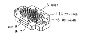
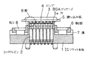
参考形態のICソケットは図1から図4に示すように、相対する平行な2面を少なくとも持つように一体成形されたICソケット本体1からなる。特に図4に示すように、ICソケット本体1には複数のコンタクトピン(C/P)2がBGAパッケージ3のバンプ(半田ボール)4の配置に対応して、ICソケット本体1の相対する平行な2面に対して垂直に埋め込まれている。各コンタクトピン2の先端部はそれぞれ、ICソケット本体1の相対する平行な2面のうちの一方の面から突き出ており、しかも各コンタクトピン2の中に入っているスプリング(不図示)により外側に向かって付勢されていて、そのスプリング(不図示)の付勢力に抗して外部から押さえられると内部へ引っ込むものとなっている。
【0012】
ICソケット本体1の、コンタクトピン2の先端部が突き出た面部(前記のICソケット本体1の相対する平行な2面のうちの一方の面)と対向する箇所には、BGAパッケージ3の各バンプ4の配置及び外形に対応させた複数の穴5aを持つ平板状の誘い込み板5が浮かぶように支持されている。しかもこの時、各コンタクトピン2の先端部は誘い込み板5の各穴5aから突き出ないように、各穴5aの中に位置している。また、各バンプ4の中心を各コンタクトピン2の先端部の外形の範囲内に確実に誘い込めるように、各穴5aの開口縁はテーパ形状となっている。
【0013】
上記のように誘い込み板5を浮かせた状態で支持するために本形態では、誘い込み板5の相対する側部にそれぞれ平板状の脚部6が、誘い込み板5と高さを変えて平行になるように一体成形もしくは組付けられている。そして各脚部6はスプリング9(図3参照)によりICソケット本体1に対して浮くように押し上げられ、脚部6を貫通してICソケット本体1とねじ合うねじ8の頭により所定の高さで静止している。このようにして脚部6が設けられた誘い込み板5は浮いた状態になっており、ねじ8の変更によりフローティング高さを調整することができる。
【0014】
上述したような形態では、BGAパッケージ3のバンプ4をそれぞれ誘い込み板5の穴5aに入れていくと、バンプ4はコンタクトピン2と接触する前に穴5aによりコンタクトピン2の先端部へと案内されて、図5に示すようにバンプ4の中心がコンタクトピン2の先端部の外形の範囲内で位置決めされる。その後、BGAパッケージ3と共に誘い込み板5をICソケット本体1の側へと押し付けると、バンプ4は誘い込み板5の穴5aにより正確な位置を確保しながらコンタクトピン2と接続される。このため、コンタクトミスをなくすことができる。
【0015】
なお、本形態において、ICソケット本体1には、誘い込み板5をICソケット本体1に近付けた時に脚部6の移動範囲がICソケット本体1で規制されないように、脚部6が入り込む溝7が形成されていてもよい。また、本形態のように平板状の脚部6の高さを誘い込み板5と変えているのは、BGAパッケージ3と共に誘い込み板5をICソケット本体1の側へ移動させた際に、ねじ8の頭にBGAパッケージ3の外周部が当たらないようにする為である。しかし、ねじ8がBGAパッケージ3と当たらない位置にあれば、脚部6と誘い込み板5とは同一高さにあってもよいのは勿論の事である。
【0016】
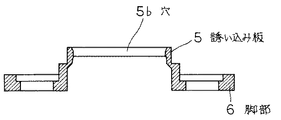
以上説明したように参考形態では、誘い込み板5に、各バンプ4の配置及び外形に対応させた複数の穴5aを形成してあるが、これに代わり、本発明の実施形態は、図6に示すように誘い込み板5に、BGAパッケージ3に設けられた複数のバンプ4で画する外周に合わせて一つの穴5bを開け、その穴5bの開口縁を、各バンプ4の中心を各コンタクトピン2の先端部の外形の範囲内で誘い込めるようにテーパ形状にしたものである。
【0017】
【発明の効果】
以上説明したように本発明は、相対する平行な2面を少なくとも持つソケット本体に複数のコンタクトピンをBGAパッケージの複数のボールバンプの配置に対応して埋め込み、各コンタクトピンの先端部をそれぞれ前記平行な2面のうちの一方の面から突出させ、前記平行な2面のうちの一方の面と対向する箇所に、前記各ボールバンプの中心を前記各コンタクトピンの先端部の外形の範囲内で誘い込める穴を持つ平板状の誘い込み板を、浮いた状態で弾性的に支持した構造としたことにより、コンタクト前にバンプを穴によってコンタクトピンの先端部へと案内し、バンプの中心をコンタクトピンの先端部の外形の範囲内で位置決めすることができるので、コンタクトミスをなくすことができる。
【図面の簡単な説明】
【図1】本発明の参考形態であるICソケットを示す全体斜視図である。
【図2】図1に示したICソケットの平面図である。
【図3】図1に示したICソケットの側面図である。
【図4】図2のA−A’線断面図である。
【図5】図4中のB部の詳細図である。
【図6】本発明の実施形態における誘い込み板を示す断面図である。
【図7】従来の、BGAパッケージ用のICソケットの構造を示す縦断面図である。
【図8】従来のICソケットにおいて、BGAパッケージのバンプが確実にコンタクトされた時の様子を示す断面図である。
【図9】図7に示したA部の詳細図である。
【符号の説明】
1 ICソケット本体
2 コンタクトピン
3 BGAパッケージ
4 バンプ
5 誘い込み板
5a、5b 穴
6 脚部
7 溝
8 ねじ
9 スプリング[0001]
BACKGROUND OF THE INVENTION
The present invention relates to an IC socket used for testing the performance and function of a device of a BGA (Ball Grid Array) package, and in particular, a bump which is an external terminal of the device is securely connected to a contact pin (C / P) of the IC socket. The present invention relates to an IC socket provided with a positioning guide mechanism for guiding.
[0002]
[Prior art]
A conventional structure of this type of IC socket for a BGA package is shown in FIG. 7 in a longitudinal sectional view, and FIG. 8 is a longitudinal sectional view showing a state in which the bumps of the BGA package are reliably contacted. FIG. 9 shows a detailed view of a portion A in FIG.
[0003]
As shown in FIG. 7, the conventional IC socket for a BGA package includes an IC socket body 102 that is integrally molded so as to have at least two opposing parallel surfaces. In this IC socket body 102, a plurality of contact pins (C / P) 104 correspond to the arrangement of ball bumps (solder balls) 102 that are external terminals of the BGA package 101, and the parallel two parallel pins of the IC socket body 1. Embedded perpendicular to the surface. The tip of each contact pin 104 protrudes from one of two opposing parallel surfaces of the IC socket body 102, and the periphery of the tip of each contact pin 104 on one of the surfaces is The ball bump 102 is cut out in a mortar shape as a lead-in portion 105. The tip of each contact pin 104 is urged outward by a spring (not shown) contained in each contact pin 104, and is pressed from the outside against the urging force of the spring. It is designed to retract inside. Therefore, as shown in FIG. 8, if the ball bump 102 is correctly placed on the tip of the contact pin 104, the bump 102 can contact the contact pin 104 along the guiding portion 105.
[0004]
[Problems to be solved by the invention]
However, the IC socket as described above has a structure in which the bump of the device contacts the contact pin (C / P) before the lead-in portion of the IC socket at the time of contact. Therefore, as shown in FIG. 9, when the center of the bump is deviated from the outer shape (D) of the contact pin, it is difficult to correct the position by the lead-in portion of the IC socket, which causes a contact error.
[0005]
Accordingly, an object of the present invention is to provide an IC socket capable of ensuring an accurate contact position when testing the performance and function of a device of a BGA package in view of the above-described problems of the prior art.
[0006]
[Means for Solving the Problems]
In order to achieve the above object, the present invention provides a socket body having at least two parallel parallel surfaces and a perpendicular to the two parallel surfaces of the socket body so as to correspond to the arrangement of a plurality of ball bumps of the BGA package. In a BGA package IC socket having a plurality of contact pins embedded and protruding from one of the two parallel surfaces, the tip portion floats with respect to the surface from which the plurality of contact pins protrude A flat guide plate elastically supported so as to be in a state of being formed, wherein one hole is formed that matches the contour defined by the outer surface of the outermost ball bump of the plurality of ball bumps The tip of each of the plurality of contact pins is accommodated, and the opening edge of the hole is at the center of each of the ball bumps at the tip of each of the contact pins. A guide plate that is tapered so that it can be guided within a range of shapes, a flat plate-like leg portion respectively disposed on opposite sides of the guide plate, and each of the leg portions to the socket body A spring that pushes up so as to float, and a screw that passes through the leg portion and is screwed with the socket body, and the floating portion of the guide plate is fixed by the head of the screw being fixed at a predetermined height. And a screw for adjusting the angle.
[0007]
In the invention configured as described above, when the ball bump of the BGA package is inserted into the hole of the guide plate, the bump is guided to the tip of the contact pin by the hole before contacting the contact pin, and the center of the bump is centered. It is positioned within the range of the outer shape of the tip of the contact pin. Thereafter, when the guide plate is pressed together with the BGA package toward the socket body, the bumps are connected to the contact pins while ensuring the correct position by the holes of the guide plate. For this reason, contact mistakes can be eliminated.
[0008]
In any of the above-described IC sockets for BGA packages, flat leg portions are provided on opposite sides of the guide plate, and each of the leg portions is floated with respect to the socket body by a spring. Thus, it is possible to apply a screw that is pushed up and is stationary at a predetermined height by a screw head that passes through the leg portion and is screwed with the socket body. In this configuration, it is possible to adjust the floating height of the guide plate by changing the screw.
[0009]
DETAILED DESCRIPTION OF THE INVENTION
Next, embodiments of the present invention will be described with reference to the drawings. Prior to the description, an IC socket as a reference embodiment of the present invention will be described with reference to FIGS.
[0010]
1 is an overall perspective view showing an IC socket as a reference embodiment of the present invention , FIG. 2 is a plan view of the IC socket shown in FIG. 1, FIG. 3 is a side view of the IC socket shown in FIG. 2 is a cross-sectional view taken along line AA ′, and FIG. 5 is a detailed view of a portion B in FIG.
[0011]
As shown in FIGS. 1 to 4, the reference type IC socket includes an IC socket body 1 that is integrally formed to have at least two parallel parallel surfaces. In particular, as shown in FIG. 4, the IC socket body 1 has a plurality of contact pins (C / P) 2 corresponding to the arrangement of the bumps (solder balls) 4 of the BGA package 3. Are embedded perpendicular to the two surfaces. The tip of each contact pin 2 protrudes from one of two parallel parallel surfaces of the IC socket body 1 and is outside by a spring (not shown) contained in each contact pin 2. When it is pressed from the outside against the biasing force of its spring (not shown), it is retracted inside.
[0012]
Each bump of the BGA package 3 is placed on a portion of the IC socket body 1 facing the surface portion (one surface of the two parallel parallel surfaces of the IC socket body 1) from which the tip of the contact pin 2 protrudes. A
[0013]
In order to support the
[0014]
In the form as described above, when the bumps 4 of the BGA package 3 are respectively inserted into the holes 5a of the
[0015]
In this embodiment, the IC socket body 1 has a
[0016]
In the above reference type state as described, the guiding
[0017]
【The invention's effect】
As described above, according to the present invention, a plurality of contact pins are embedded in a socket body having at least two opposite parallel surfaces corresponding to the arrangement of the plurality of ball bumps of the BGA package, and the tip portions of the contact pins are respectively described above. Projecting from one of the two parallel surfaces and facing the one of the two parallel surfaces, the center of each ball bump is within the range of the outer shape of the tip of each contact pin. By adopting a structure in which the flat guide plate with holes that can be inserted in is supported elastically in a floating state, the bump is guided to the tip of the contact pin by the hole before contact, and the center of the bump is contacted Since positioning can be performed within the range of the outer shape of the tip of the pin, contact mistakes can be eliminated.
[Brief description of the drawings]
FIG. 1 is an overall perspective view showing an IC socket as a reference embodiment of the present invention .
2 is a plan view of the IC socket shown in FIG. 1. FIG.
FIG. 3 is a side view of the IC socket shown in FIG. 1;
4 is a cross-sectional view taken along line AA ′ of FIG.
FIG. 5 is a detailed view of part B in FIG. 4;
FIG. 6 is a cross-sectional view showing a guide plate according to an embodiment of the present invention.
FIG. 7 is a longitudinal sectional view showing a structure of a conventional IC socket for a BGA package.
FIG. 8 is a cross-sectional view showing a state when a bump of a BGA package is reliably contacted in a conventional IC socket.
9 is a detailed view of a part A shown in FIG.
[Explanation of symbols]
1 IC socket body 2 Contact pin 3 BGA package 4
Claims (1)
BGAパッケージの複数のボールバンプの配置に対応するように前記ソケット本体に前記平行な2面に垂直に埋め込まれ、先端部が前記平行な2面のうちの一方の面から突出している複数のコンタクトピンと、を有するBGAパッケージ用ICソケットにおいて、
前記複数のコンタクトピンを突出させている面に対して浮いた状態となるように弾性的に支持された平板状の誘い込み板であって、前記複数のボールバンプのうちの最も外側のボールバンプの外側面で画される輪郭に合った一つの穴が形成されていて前記複数のコンタクトピンの先端部を収容しており、前記穴の開口縁が前記各ボールバンプの中心を前記各コンタクトピンの先端部の外形の範囲内で誘い込めるようにテーパ形状になっている誘い込み板と、
前記誘い込み板の相対する側部にそれぞれ配設された平板状の脚部と、
前記脚部の各々を前記ソケット本体に対して浮くように押し上げるスプリングと、
前記脚部を貫通して前記ソケット本体とねじ合うねじであって、ねじの頭により前記脚部を所定の高さで静止させて前記誘い込み板のフローティング高さを調節するねじと、
をさらに備えたことを特徴とするBGAパッケージ用ICソケット。A socket body having at least two opposite parallel surfaces;
A plurality of contacts embedded in the socket body perpendicularly to the two parallel surfaces so as to correspond to the arrangement of the plurality of ball bumps of the BGA package, and having tips that protrude from one of the two parallel surfaces In an IC socket for a BGA package having a pin,
A flat guide plate elastically supported so as to be in a floating state with respect to a surface from which the plurality of contact pins protrude, wherein the outermost ball bump of the plurality of ball bumps One hole that matches the contour defined on the outer surface is formed to accommodate the tip ends of the plurality of contact pins, and the opening edges of the holes center the centers of the ball bumps. A guide plate having a tapered shape so that it can be guided within the range of the outer shape of the tip,
Flat plate-like leg portions respectively disposed on opposite sides of the guide plate;
A spring that pushes up each of the legs so as to float with respect to the socket body;
A screw that passes through the leg portion and is screwed with the socket body, and a screw that adjusts the floating height of the guide plate by stopping the leg portion at a predetermined height by a screw head;
An IC socket for a BGA package, further comprising:
Priority Applications (9)
| Application Number | Priority Date | Filing Date | Title |
|---|---|---|---|
| JP30469496A JP3761997B2 (en) | 1996-11-15 | 1996-11-15 | IC socket for BGA package |
| US08/963,859 US6036503A (en) | 1996-11-15 | 1997-11-04 | IC socket for a BGA package |
| GB9723314A GB2319404B (en) | 1996-11-15 | 1997-11-04 | IC socket for BGA package |
| SG1997003992A SG54591A1 (en) | 1996-11-15 | 1997-11-07 | Ic socket for a bga package |
| TW086116792A TW353799B (en) | 1996-11-15 | 1997-11-11 | IC socket for a BGA package |
| KR1019970059191A KR100268983B1 (en) | 1996-11-15 | 1997-11-11 | Ic socket for a bga package |
| DE19750323A DE19750323C2 (en) | 1996-11-15 | 1997-11-13 | IC socket for a BGA package |
| MYPI97005410A MY123841A (en) | 1996-11-15 | 1997-11-13 | Ic socket for a bga package |
| CN97114155A CN1185047A (en) | 1996-11-15 | 1997-11-15 | IC socket for BGA package |
Applications Claiming Priority (1)
| Application Number | Priority Date | Filing Date | Title |
|---|---|---|---|
| JP30469496A JP3761997B2 (en) | 1996-11-15 | 1996-11-15 | IC socket for BGA package |
Publications (2)
| Publication Number | Publication Date |
|---|---|
| JPH10144439A JPH10144439A (en) | 1998-05-29 |
| JP3761997B2 true JP3761997B2 (en) | 2006-03-29 |
Family
ID=17936099
Family Applications (1)
| Application Number | Title | Priority Date | Filing Date |
|---|---|---|---|
| JP30469496A Expired - Fee Related JP3761997B2 (en) | 1996-11-15 | 1996-11-15 | IC socket for BGA package |
Country Status (9)
| Country | Link |
|---|---|
| US (1) | US6036503A (en) |
| JP (1) | JP3761997B2 (en) |
| KR (1) | KR100268983B1 (en) |
| CN (1) | CN1185047A (en) |
| DE (1) | DE19750323C2 (en) |
| GB (1) | GB2319404B (en) |
| MY (1) | MY123841A (en) |
| SG (1) | SG54591A1 (en) |
| TW (1) | TW353799B (en) |
Families Citing this family (38)
| Publication number | Priority date | Publication date | Assignee | Title |
|---|---|---|---|---|
| US6048744A (en) | 1997-09-15 | 2000-04-11 | Micron Technology, Inc. | Integrated circuit package alignment feature |
| JPH11233216A (en) * | 1998-02-16 | 1999-08-27 | Nippon Denki Factory Engineering Kk | Ic socket for test |
| US6283780B1 (en) * | 1998-04-01 | 2001-09-04 | Molex Incorporated | Test socket lattice |
| US6502221B1 (en) | 1998-07-14 | 2002-12-31 | Nvidia Corporation | Prototype development system |
| KR100495091B1 (en) * | 1998-09-21 | 2005-09-02 | 삼성전자주식회사 | Known Good Die carrier |
| US6565364B1 (en) * | 1998-12-23 | 2003-05-20 | Mirae Corporation | Wafer formed with CSP device and test socket of BGA device |
| KR100290734B1 (en) * | 1998-12-23 | 2001-07-12 | 정문술 | Test sockets for wafers and BGA devices with CSP devices |
| TW421333U (en) * | 1999-02-24 | 2001-02-01 | Hung Rung Fang | IC socket |
| JP3133303B2 (en) * | 1999-05-01 | 2001-02-05 | ミラエ・コーポレーション | Carrier module for micro BGA type device |
| JP2000357571A (en) * | 1999-06-14 | 2000-12-26 | Tokyo Eletec Kk | Ic socket |
| US6265886B1 (en) * | 1999-07-12 | 2001-07-24 | Micron Technology, Inc. | Conductive bump array contactors having an ejector and methods of testing using same |
| KR100631402B1 (en) * | 1999-08-25 | 2006-10-09 | 삼성전자주식회사 | UNIVASAL SOCKET FOR BGABall Grid Array PACKAGE AND PACKAGE TEST METHOD BY USING THEREOF |
| KR20010054178A (en) * | 1999-12-03 | 2001-07-02 | 송재인 | Ic socket for ball grid array |
| US6464513B1 (en) * | 2000-01-05 | 2002-10-15 | Micron Technology, Inc. | Adapter for non-permanently connecting integrated circuit devices to multi-chip modules and method of using same |
| US6407566B1 (en) | 2000-04-06 | 2002-06-18 | Micron Technology, Inc. | Test module for multi-chip module simulation testing of integrated circuit packages |
| KR20010105854A (en) * | 2000-05-19 | 2001-11-29 | 이영희 | Integrated circuit socket |
| JP3921163B2 (en) * | 2000-09-26 | 2007-05-30 | 株式会社アドバンストシステムズジャパン | Spiral contactor, manufacturing method thereof, semiconductor inspection apparatus using the same, and electronic component |
| JP2002373748A (en) * | 2001-06-14 | 2002-12-26 | Yamaichi Electronics Co Ltd | Socket for semiconductor device |
| JPWO2003007435A1 (en) | 2001-07-13 | 2004-11-04 | 日本発条株式会社 | Contactor |
| US7045889B2 (en) * | 2001-08-21 | 2006-05-16 | Micron Technology, Inc. | Device for establishing non-permanent electrical connection between an integrated circuit device lead element and a substrate |
| US7049693B2 (en) | 2001-08-29 | 2006-05-23 | Micron Technology, Inc. | Electrical contact array for substrate assemblies |
| US6991960B2 (en) * | 2001-08-30 | 2006-01-31 | Micron Technology, Inc. | Method of semiconductor device package alignment and method of testing |
| US6769919B2 (en) * | 2002-09-04 | 2004-08-03 | Itt Manufacturing Enterprises, Inc. | Low profile and low resistance connector |
| JP3768183B2 (en) * | 2002-10-28 | 2006-04-19 | 山一電機株式会社 | IC socket for narrow pitch IC package |
| US6861862B1 (en) | 2003-03-17 | 2005-03-01 | John O. Tate | Test socket |
| TWI239695B (en) * | 2003-08-11 | 2005-09-11 | Speed Tech Corp | Matrix connector |
| CN1306662C (en) * | 2003-08-27 | 2007-03-21 | 宣得股份有限公司 | Matrix connector |
| KR100602442B1 (en) * | 2004-05-18 | 2006-07-19 | 삼성전자주식회사 | Test socket having connecting substrate |
| TWM266611U (en) * | 2004-07-16 | 2005-06-01 | Hon Hai Prec Ind Co Ltd | Electrical connector |
| US7108535B1 (en) | 2005-07-12 | 2006-09-19 | Spansion, Llc | Integrated circuit test socket |
| US20070126445A1 (en) * | 2005-11-30 | 2007-06-07 | Micron Technology, Inc. | Integrated circuit package testing devices and methods of making and using same |
| TWI385773B (en) * | 2008-05-21 | 2013-02-11 | Lefram Technology Corp | Lead frame carrier and method of manufacturing the same |
| TWM359860U (en) * | 2008-11-25 | 2009-06-21 | Hon Hai Prec Ind Co Ltd | Electrical connector |
| JP5564304B2 (en) * | 2010-03-29 | 2014-07-30 | 株式会社エンプラス | Socket for electrical parts |
| JP5865846B2 (en) * | 2011-01-19 | 2016-02-17 | ユニテクノ株式会社 | Inspection socket |
| KR101217205B1 (en) | 2011-09-23 | 2012-12-31 | 하이콘 주식회사 | Socket device for testing an ic |
| JP2013137286A (en) * | 2011-12-28 | 2013-07-11 | Advantest Corp | Electronic component testing device |
| US8764458B1 (en) * | 2012-09-10 | 2014-07-01 | Amazon Technologies, Inc. | Spring connector and corresponding guide element |
Family Cites Families (14)
| Publication number | Priority date | Publication date | Assignee | Title |
|---|---|---|---|---|
| JP2509285B2 (en) * | 1988-03-18 | 1996-06-19 | 富士通株式会社 | Semiconductor device testing method |
| JPH05129478A (en) * | 1991-11-06 | 1993-05-25 | Hitachi Ltd | Socket with function for removing foreign matter from lead |
| US5247250A (en) * | 1992-03-27 | 1993-09-21 | Minnesota Mining And Manufacturing Company | Integrated circuit test socket |
| EP0616394A1 (en) * | 1993-03-16 | 1994-09-21 | Hewlett-Packard Company | Method and system for producing electrically interconnected circuits |
| US5518410A (en) * | 1993-05-24 | 1996-05-21 | Enplas Corporation | Contact pin device for IC sockets |
| US5500605A (en) * | 1993-09-17 | 1996-03-19 | At&T Corp. | Electrical test apparatus and method |
| US5376010A (en) * | 1994-02-08 | 1994-12-27 | Minnesota Mining And Manufacturing Company | Burn-in socket |
| JP2648120B2 (en) * | 1995-02-08 | 1997-08-27 | 山一電機株式会社 | Surface contact type connector |
| US5570033A (en) * | 1995-07-20 | 1996-10-29 | Vlsi Technology, Inc. | Spring probe BGA (ball grid array) contactor with device stop and method therefor |
| JP3518091B2 (en) * | 1995-09-25 | 2004-04-12 | 株式会社エンプラス | IC socket |
| US5702255A (en) * | 1995-11-03 | 1997-12-30 | Advanced Interconnections Corporation | Ball grid array socket assembly |
| US5791914A (en) * | 1995-11-21 | 1998-08-11 | Loranger International Corporation | Electrical socket with floating guide plate |
| US5730606A (en) * | 1996-04-02 | 1998-03-24 | Aries Electronics, Inc. | Universal production ball grid array socket |
| JP3042408B2 (en) * | 1996-07-08 | 2000-05-15 | 日本電気株式会社 | Semiconductor device measuring method and measuring jig |
-
1996
- 1996-11-15 JP JP30469496A patent/JP3761997B2/en not_active Expired - Fee Related
-
1997
- 1997-11-04 US US08/963,859 patent/US6036503A/en not_active Expired - Fee Related
- 1997-11-04 GB GB9723314A patent/GB2319404B/en not_active Expired - Fee Related
- 1997-11-07 SG SG1997003992A patent/SG54591A1/en unknown
- 1997-11-11 TW TW086116792A patent/TW353799B/en not_active IP Right Cessation
- 1997-11-11 KR KR1019970059191A patent/KR100268983B1/en not_active IP Right Cessation
- 1997-11-13 DE DE19750323A patent/DE19750323C2/en not_active Expired - Fee Related
- 1997-11-13 MY MYPI97005410A patent/MY123841A/en unknown
- 1997-11-15 CN CN97114155A patent/CN1185047A/en active Pending
Also Published As
| Publication number | Publication date |
|---|---|
| JPH10144439A (en) | 1998-05-29 |
| MY123841A (en) | 2006-06-30 |
| CN1185047A (en) | 1998-06-17 |
| DE19750323A1 (en) | 1998-05-28 |
| KR100268983B1 (en) | 2000-10-16 |
| DE19750323C2 (en) | 2003-04-30 |
| US6036503A (en) | 2000-03-14 |
| SG54591A1 (en) | 1998-11-16 |
| KR19980042274A (en) | 1998-08-17 |
| GB2319404B (en) | 1998-10-28 |
| TW353799B (en) | 1999-03-01 |
| GB9723314D0 (en) | 1998-01-07 |
| GB2319404A (en) | 1998-05-20 |
Similar Documents
| Publication | Publication Date | Title |
|---|---|---|
| JP3761997B2 (en) | IC socket for BGA package | |
| USRE35693E (en) | Leadless chip carrier socket | |
| US6848928B2 (en) | Socket | |
| US4678255A (en) | Chip connector | |
| US6069481A (en) | Socket for measuring a ball grid array semiconductor | |
| JPS63305537A (en) | Socket device | |
| US9766268B2 (en) | Contactor with angled spring probes | |
| KR101852794B1 (en) | Apparatus for testing semiconductor package | |
| JPS5950551A (en) | Socket for integrated circuit element test | |
| JP3017180B1 (en) | Contact pins and sockets | |
| JP4464250B2 (en) | Socket for electrical parts | |
| US20090289652A1 (en) | Pogo probe, probe socket, and probe card | |
| US20080220627A1 (en) | IC package having improved structure | |
| TWI766154B (en) | Probe head and probe card | |
| TWM514004U (en) | Integrated circuit inspection device and inspection equipment | |
| US6293809B1 (en) | Socket for electrical parts | |
| US6447318B1 (en) | Socket for electrical parts | |
| KR100773194B1 (en) | Socket for BGA package | |
| KR20000001126U (en) | Solder Ball Guide Structure in Test Sockets for Ball Grid Array Packages | |
| JP3266530B2 (en) | socket | |
| JP4038828B2 (en) | IC socket | |
| US7833043B2 (en) | Socket connector | |
| US20010046127A1 (en) | Semiconductor package and device socket | |
| US10101361B2 (en) | Method for testing semiconductor devices | |
| JP2007317365A (en) | Socket for electric component |
Legal Events
| Date | Code | Title | Description |
|---|---|---|---|
| A977 | Report on retrieval |
Free format text: JAPANESE INTERMEDIATE CODE: A971007 Effective date: 20050405 |
|
| A131 | Notification of reasons for refusal |
Free format text: JAPANESE INTERMEDIATE CODE: A131 Effective date: 20050413 |
|
| A521 | Request for written amendment filed |
Free format text: JAPANESE INTERMEDIATE CODE: A523 Effective date: 20050610 |
|
| RD03 | Notification of appointment of power of attorney |
Free format text: JAPANESE INTERMEDIATE CODE: A7423 Effective date: 20050610 |
|
| A131 | Notification of reasons for refusal |
Free format text: JAPANESE INTERMEDIATE CODE: A131 Effective date: 20050810 |
|
| A521 | Request for written amendment filed |
Free format text: JAPANESE INTERMEDIATE CODE: A523 Effective date: 20050902 |
|
| TRDD | Decision of grant or rejection written | ||
| A01 | Written decision to grant a patent or to grant a registration (utility model) |
Free format text: JAPANESE INTERMEDIATE CODE: A01 Effective date: 20051214 |
|
| A61 | First payment of annual fees (during grant procedure) |
Free format text: JAPANESE INTERMEDIATE CODE: A61 Effective date: 20060112 |
|
| R150 | Certificate of patent or registration of utility model |
Free format text: JAPANESE INTERMEDIATE CODE: R150 |
|
| FPAY | Renewal fee payment (event date is renewal date of database) |
Free format text: PAYMENT UNTIL: 20090120 Year of fee payment: 3 |
|
| FPAY | Renewal fee payment (event date is renewal date of database) |
Free format text: PAYMENT UNTIL: 20100120 Year of fee payment: 4 |
|
| FPAY | Renewal fee payment (event date is renewal date of database) |
Free format text: PAYMENT UNTIL: 20110120 Year of fee payment: 5 |
|
| LAPS | Cancellation because of no payment of annual fees |