JP3754080B2 - Method, code device, and recording device for converting m-bit information word sequence into modulation signal - Google Patents
Method, code device, and recording device for converting m-bit information word sequence into modulation signal Download PDFInfo
- Publication number
- JP3754080B2 JP3754080B2 JP51101997A JP51101997A JP3754080B2 JP 3754080 B2 JP3754080 B2 JP 3754080B2 JP 51101997 A JP51101997 A JP 51101997A JP 51101997 A JP51101997 A JP 51101997A JP 3754080 B2 JP3754080 B2 JP 3754080B2
- Authority
- JP
- Japan
- Prior art keywords
- code
- word
- type
- state
- information
- Prior art date
- Legal status (The legal status is an assumption and is not a legal conclusion. Google has not performed a legal analysis and makes no representation as to the accuracy of the status listed.)
- Expired - Lifetime
Links
Images


Classifications
-
- G—PHYSICS
- G11—INFORMATION STORAGE
- G11B—INFORMATION STORAGE BASED ON RELATIVE MOVEMENT BETWEEN RECORD CARRIER AND TRANSDUCER
- G11B20/00—Signal processing not specific to the method of recording or reproducing; Circuits therefor
- G11B20/10—Digital recording or reproducing
- G11B20/14—Digital recording or reproducing using self-clocking codes
-
- H—ELECTRICITY
- H03—ELECTRONIC CIRCUITRY
- H03M—CODING; DECODING; CODE CONVERSION IN GENERAL
- H03M5/00—Conversion of the form of the representation of individual digits
- H03M5/02—Conversion to or from representation by pulses
- H03M5/04—Conversion to or from representation by pulses the pulses having two levels
- H03M5/14—Code representation, e.g. transition, for a given bit cell depending on the information in one or more adjacent bit cells, e.g. delay modulation code, double density code
- H03M5/145—Conversion to or from block codes or representations thereof
-
- G—PHYSICS
- G11—INFORMATION STORAGE
- G11B—INFORMATION STORAGE BASED ON RELATIVE MOVEMENT BETWEEN RECORD CARRIER AND TRANSDUCER
- G11B20/00—Signal processing not specific to the method of recording or reproducing; Circuits therefor
- G11B20/10—Digital recording or reproducing
- G11B20/14—Digital recording or reproducing using self-clocking codes
- G11B20/1403—Digital recording or reproducing using self-clocking codes characterised by the use of two levels
- G11B20/1423—Code representation depending on subsequent bits, e.g. delay modulation, double density code, Miller code
- G11B20/1426—Code representation depending on subsequent bits, e.g. delay modulation, double density code, Miller code conversion to or from block codes or representations thereof
-
- H—ELECTRICITY
- H03—ELECTRONIC CIRCUITRY
- H03M—CODING; DECODING; CODE CONVERSION IN GENERAL
- H03M5/00—Conversion of the form of the representation of individual digits
- H03M5/02—Conversion to or from representation by pulses
- H03M5/04—Conversion to or from representation by pulses the pulses having two levels
- H03M5/14—Code representation, e.g. transition, for a given bit cell depending on the information in one or more adjacent bit cells, e.g. delay modulation code, double density code
-
- H—ELECTRICITY
- H03—ELECTRONIC CIRCUITRY
- H03M—CODING; DECODING; CODE CONVERSION IN GENERAL
- H03M7/00—Conversion of a code where information is represented by a given sequence or number of digits to a code where the same, similar or subset of information is represented by a different sequence or number of digits
-
- G—PHYSICS
- G11—INFORMATION STORAGE
- G11B—INFORMATION STORAGE BASED ON RELATIVE MOVEMENT BETWEEN RECORD CARRIER AND TRANSDUCER
- G11B20/00—Signal processing not specific to the method of recording or reproducing; Circuits therefor
- G11B20/10—Digital recording or reproducing
- G11B20/14—Digital recording or reproducing using self-clocking codes
- G11B20/1403—Digital recording or reproducing using self-clocking codes characterised by the use of two levels
- G11B20/1423—Code representation depending on subsequent bits, e.g. delay modulation, double density code, Miller code
- G11B20/1426—Code representation depending on subsequent bits, e.g. delay modulation, double density code, Miller code conversion to or from block codes or representations thereof
- G11B2020/1461—8 to 14 modulation, e.g. the EFM code used on CDs or mini-discs
Landscapes
- Engineering & Computer Science (AREA)
- Theoretical Computer Science (AREA)
- Signal Processing (AREA)
- Signal Processing For Digital Recording And Reproducing (AREA)
- Digital Transmission Methods That Use Modulated Carrier Waves (AREA)
- Optical Recording Or Reproduction (AREA)
Abstract
Description
技術分野
本発明は、mが整数であるmビット情報語の系列を変調信号に変換する方法であって、対応する前記変調信号が所定の基準を満たすように前記情報語の系列が変換規則に従ってnがmを越える整数であるnビットのコード語の系列に変換されて出力される工程と、出力された前記コード語が前記変調信号に変調される工程とを有し、前記変換工程において、前記コード語は少なくとも第1型の群と少なくとも第2型の群とに分散する一方、前記第1型の群に属する前記コード語の各々の出力は、対応する群により決定される第1型のコード状態を生成し、前記第2型の群に属する前記コード語の各々の出力は、対応する群と出力された前記コード語に対応する前記情報語とにより決定される第2型のコード状態を生成し、前記コード語の一つが入力された前記情報語に割り当てられる場合、このコード語は先行するコード語が出力された際に生成された前記コード状態に依存するコード語の組から選択される一方、前記第2型の前記コード状態に属するコード語の組は如何なるコード語も共通に有さず、前記第2型の前記群は複数の情報語と関連するコード語を少なくとも一つ有し、それぞれの情報語は後続するコード語を検出することにより区別されるような方法に関する。
本発明は、上記方法により得られる信号を記録キャリアに供給する方法にも関する。
本発明は、更に、請求項に記載の方法を実施するコード装置にも関し、当該装置はmビット情報語をnビットコード語に変換するm/nビット変換器と、これらnビットコード語を変調信号に変換する手段とを有している。
本発明は、更に、このような形式のコード装置が使用されるような記録装置にも関する。
本発明は、更に、信号にも関する。
本発明は、更に、前記信号が記録される記録キャリアにも関する。
背景技術
上記のような方法、装置、記録キャリア及び信号は、(ヨーロッパ特許公報第EP-A-94200387.2号,PHN14746に対応する)WO 95/22802から既知である。前記公報はmビット情報語の系列を変調信号に変換する方法に関し、前記方法はEFM+と呼ばれる。前記系列からの情報語の各々に対してnビットコード語は出力される。前記出力されたコード語は、変調信号に変換される。前記コード語は少なくとも第1型の一つの群と少なくとも第2型の一つの群とに分布される。前記第1型の群に属する各コード語の出力に対し、対応する群は第1型のコード状態を生成する。前記第2型の群に属するコード語が出力される場合、前記第2型のコード状態が生成される。コード語は生成されたコード状態に依存するコード語の組から選択される入力された情報語に割り当てられる。第2型のコード状態に属するコード語の組は分離している。可能な第2型のコードの組の選択される一つは、出力されたコード語に対応する前記情報語により決定される。これは同様のコード語と対応する情報語のいくつかを異なる前記生成されたコード状態にするのを許容する。このコード方法において、前記系列におけるコード語で使用される特定なビットの組合せ数は増加し、それによりコード効率が増加する。よって得られた変調信号は、最初に当該変調信号をコード語の系列に変換し、次に変換されるべきコード語に依存及び前記コード語に関係する所定の位置にあるビット列のビットの論理値にも依存する系列からのコード語の各々に情報語を割り当てることにより当該情報語を再変換してもよい。当該論理値は先行して生成されるコード状態に対する表示である。更に、記録装置及び読取装置が開示される。
前記変調信号の低周波数成分は、記録システムにおけるサーボ信号のような他のシステムパラメータで防止してもよい。たとえ上記変換方法が制限された低周波数の内容を持つ変調信号であっても、低周波数成分を減少するのにまだ必要である。
発明の開示
よって本発明は、前記変調信号の低周波数の内容を低減するのに適した変換を行う手段を提供することを目的とする。
本発明の第1の見方によれば、本目的は、第1型のコード状態を生成した後、所定の基準に従う一方で、前記変調信号の低周波数の内容への依存して、コード語は前記生成したコード状態に属する組から又は異なる第1型のコード状態に依存する組から選択されることを特徴とする冒頭で述べた方法により達成される。
本発明の第2の見方によれば、本目的は、記録キャリア、コード装置、記録装置及び記録キャリアを製造する方法を用いて達成される。本発明による対策は、前記変調信号の(時々DCと呼ばれる)低周波数の内容が減少される一方、同様の情報コード効果を保つという利点を有する。
【図面の簡単な説明】
以下、本発明を第1図〜第9図を参照して説明するが、これら図面において、
第1図は、情報語の系列、対応するコード語の系列及び変調信号を示し、
第2図は、記録キャリアを示し、
第3図は、第2図の記録キャリアの拡大部を示し、
第4図は、記録装置を示し、
第5図は、デコード及び再生装置を示し、
第6図は、コード装置を示し、
第7図及び第8図は、情報語とコード語との間の関係を表すテーブルを示し、及び
第9図は、変調信号の周波数スペクトルを示す。
発明を実施するための最良の形態
第1図は、3個の連続したmビット情報語、この場合は1で示す8ビット情報語を示している。コード方法についての情報は、K.A. Schouhamer Imminkによる"Cording Techniques for Digital Recorders"(ISBN 0-13-140047-9)という題名の文献中で見られる。この文献には、例えば、いわゆるEFM変調システムが記載され、該システムは情報をいわゆるコンパクトディスクに記録するために使用される。EFM変調信号は8ビット情報語の系列を14ビットコード語の系列に変換することにより得られ、この場合3個の余裕ビットが各コード語の間に挿入される。これらコード語は、「1」ビット間の「0」ビットの最小数がd(2)となり、最大数がk(10)となるように選択される。この制約条件は、dk制約条件とも呼ばれる。上記コード語の系列はモジュロ2積分演算によりハイ又はロー信号値を持つビットセルにより形成される対応する信号に変換され、この変調された信号(変調信号)においては「1」ビットはハイからロー信号値への変化又はその逆の変化により表される。一方、「0」ビットは2つのビットセルの間の遷移部において信号値の変化が無いことにより表される。前記余裕ビットは、2つのコード語の間の遷移領域においてさえもdk制約条件が満たされ、且つ、対応する信号中において、いわゆるランニングデジタル合計値がほぼ一定となるように、選択される。特定の瞬時における上記ランニングデジタル合計値は、変調信号の当該瞬時以前に位置する部分にわたって計算される、ハイ信号値を持つビットセルの数とロー信号値を持つビットセルの数との間の差を意味するものと理解される。ほぼ一定のランニングデジタル合計値は、当該信号の周波数スペクトルが低周波数領域での周波数成分を持たない、ということを意味する。このような信号はDCフリー信号とも呼ばれる。信号中に低周波数成分が無いことは、トラック中に信号が記録された記録キャリアから当該信号が読み出される場合に非常に有利である。何故なら、この場合に上記の記録された信号により影響を受けない連続したトラッキング制御が可能となるからである。一方、情報の記録は、記録キャリア上の情報密度の向上を常に必要としている。第1図において、これら3個の情報語1は、語値「24」、「121」、及び「34」を各々有している。この3個の情報語1の系列は3個の連続したnビットコード語、この場合は4で示す16ビットコード語、に変換される。コード語4は論理値「0」を持つビットと、論理値「1」を持つビットとのビット列を形成する。情報信号の上記変換は、当該ビット列において、論理値「1」を持つ2つのビットの間に位置する論理値「0」を持つビットの最小数がdであり、最大数がkであり、ここでdが2に等しくkが10に等くなるようなものである。このようなビット列は、しばしば、dk制約条件を伴うRLL(Run Length Limited)列と呼ばれる。更に、各コード語の個々のビットはx1はx1,…,x16で示され、ここでx1は当該コード語の(左から)最初のビットを示し、x16は当該コード語の最終ビットを示す。
コード語4により形成された上記ビット列はモジュロ2積分演算により変調信号7に変換される。この変調信号は前記各コード語4を表す3個の情報信号部8を有している。各情報信号部は、ハイ信号値H又はロー信号値Lを持つことのできるビットセル11を有している。情報信号部当たりのビットセルの数は、対応するコード語のビット数に等しい。論理値「1」を持つ各コード語ビットは。変調信号7においては、ハイ信号値を持つビットセルからロー信号値を持つビットセルへの又はその逆の遷移により示される。論理値「0」を持つ各コード語ビットは、変調信号7においては、ビットセルの遷移部において信号値の変化が無いものとして示される。
更に、上記変調信号7の周波数スペクトルはほぼ何の低周波数成分も含まないことが要求される。言い換えると、変調信号7はDCフリーであるべきである。
以下においては、変調信号が得られる本発明による方法の一実施例を詳細に説明する。
まず始めに、コード語に対しては、dk制約条件が満たされる、という要求が存在する。dk制約条件を満たす可能な全てのコード語の群は、少なくとも第1型の群と少なくとも第2型の群とに分割される。コード語が第1型の群の一つから供給される場合、供給されたコード語が属する第1型の群に排他的に依存するコード状態が設定される。第1型の群のコード語の一つが供給される場合、第1型の群と供給されたコード語で示された情報語の両者に依存してコード状態が設定される。この実施例においては、第1型の2つの群、例えば、論理値「0」を持つaビット(aは、0もしくは1)で終了するコード語を有する第1群G11、そして論理値「0」を持つbビット(bは、9以下6以上の整数)で終了するコード語第2群G12を区別できる。
第1型の第1群G11により設定されたコード状態は、以後、参照符号S1で参照される。第1型の第2群G12により設定されたコード状態は、以後、参照符号S4で参照される。ここで述べた実施例は、1個の第2型の群のみしか知らない。この群は、論理値「0」を持つcビット(cは、2以上5以下の整数)で終了するコード語を有する。この群は、以後、群G2として参照されるであろう。ここに記述された実施例において、例えばS2、S3である2つのコード状態を、コード語と対応する情報語との組み合わせにより設定できる。
情報語がコード語に変換される場合、コード状態に依存するコード語の群に属するコード語が、変換されるべき情報語に割当てられる。コード状態S1,S2,S3,S4に属するコード語の群は、以後、それぞれ参照符号V1,V2,V3,V4で参照される。前記群のコード語は、コード状態が設定された群からのコード語と、このコード状態により設定された群からの任意のコード語とにより形成可能な各ビット列がdk制約条件を満たすように選択される。コード状態S4が先に供給したコード語の供給によって設定され、そしてこのコード状態が6以上9以下の論理値「0」を持つaビット列で先行するコード語が終了することを示す場合、コード状態S4により設定されたコード語群V4は、論理値「0」を持つ最大1ビットで始まるコード語を有することのみが許容される。この事柄のため、論理値「0」を持つ多数のビットで始まるコード語は、先行して供給したコード語と供給されるべきコード語との間の推移領域を持つであろう。この領域において、論理値「0」を持つ連続ビットの数は、常に10以下ではなく、従って、dk制約条件を満たすことはない。同様な理由から、組V1は、2以上9以下の論理値「0」を持つ多数のビットで始まるコード語のみを有する。
コード状態S2及びS3に属するコード語の組V2及びV3は、0以上5以下の論理値「0」を持つ多数のビットで始まるコード語のみを含む。この状態を満たすコード語は、2つの組V2,V3に分散され、この結果、組V2,V3は、如何なる共通コード語も全く含まない。組V2,V3は、以下においては、分離された組として参照されるであろう。組V2,V3におけるコード語の分散は、望ましくは、pビットなる限定された数の論理値に基づいて、コード語が何処の組に属するかを規定できるようなものにする。上述の例において、ビット結合x1.x13が、この目的のために使用される。組V2からのコード語はビット結合x1.x13=0.0から認識可能である。組V3からのコード語は、0.0に等しくない結合x1.x13から認識可能である。供給時にコード状態S1(群G11)を設定するコード語の間、供給時にコード状態S2及びS3(群G2)を設定するコード語の間、供給時にコード状態S4(群G12)を設定するコード語の間の区別がなされる。組V1は群G11からの138個のコード語と、群G2からの96個のコード語と、そして群G12からの22個のコード語とを有する。組V1における異なるコード語の数が、異なる8ビット情報語の数よりも少なくなることが証明されるであろう。
群G2からのコード語には、常に組V2からのコード語若しくは組V3からのコード語が後続し、更に、群G2からのコード語に後続するコード語に基づいて当該コード語が何処の組に属するのかは確立されるであろうから、組V2からのコード語が後続する群G2からのコード語は、群G2からの同一コード語であるが組V3のコード語が後続するものとは明瞭に区別することができる。換言すると、コード語が情報語に割当てられた場合、群G2からの各コード語を2回使用できる。群G2からの各コード語は、組V2からのランダムなコード語と共に、同一の組V3からのランダムなコード語とにより形成されたビット結合からは分離できない固有なビット結合を形成する。これは、群G11からの138個の固有のビット結合(コード語)と、群G12からの22個の固有のビット結合(コード語)と、群G2からの2×96個の固有のビット結合(後続するコード語と結合した群G2からのコード語)とを組V1に使用することができることを意味する。この結合は、総数352の使用可能な固有ビット結合数を提供する。組V2,V3,V4からのコード語で形成した固有ビット結合の数は、それぞれ352,351及び415である。
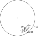
第2図は、本発明による記録キャリア120の例を示す。示された記録キャリアは、光学的検出タイプの一つである。前記記録キャリアは異なるタイプ、例えば磁気的な読み出しタイプであってもよい。前記記録キャリアは、トラック121として配される情報パターンを有する。第3図は、前記トラック121の一つの拡大された部分122を示す。第3図に示される前記トラック部121の情報パターンは、例えば光学的検出可能なマークの形式の第1区分123と、例えば当該マーク間にある中間領域の第2区分124とを有する。第1及び第2区分は、前記トラック125の方向に変換する。第1区分123は第1検出可能な特性を与え、第2区分124は第1検出可能な特性から区別可能な第2の特性を与える。第1区分123は、例えばロー信号値Lなる一方の信号レベルを持つ変調されたバイナリ信号7のビットセル12を表す。第2区分124は他方の信号レベル、例えばハイ信号値Hを持つビットセル11を表す。前記記録キャリア120は、前記変調信号を先ず発生させ、それから当該記録キャリアに前記情報パターンを供給することにより得られる。前記記録キャリアが光学的に検出可能なタイプならば、当該記録キャリアは、前記変調信号7に基づいてそれ自体既知のマスタリング及びレプリカ技術を用いて得ることができる。
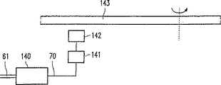
第4図は情報を記録するための記録装置を示し、例えば第6図に示されるコード装置140のような本発明に従うコード装置が用いられる。前記記録装置において、変調信号を送るための信号ラインは、記録ヘッド142のための制御回路141へ接続され、当該記録ヘッドに沿って書き込み可能なタイプの記録キャリア143に移動される。前記記録ヘッド142は、前記記録キャリア143上に検出可能な変化を持つマークを導入する従来形式のものである。前記制御回路141は、当該制御回路141に与えられる前記変調信号に応答して前記記録ヘッドに対する制御信号を発生する従来形式のものでもよいので、前記記録ヘッド142は前記変調信号に対応するマークのパターンを与える。
第5図は読取装置を示し、例えば下記に述べられるデコード装置153のような本発明に従うデコード装置が用いられる。前記読取装置は、本発明に従う記録キャリアを読むための従来形式の読取ヘッドを有し、当該記録キャリアは前記変調信号に対応する情報パターンを有する。読取ヘッド150は、当該読取ヘッドにより読み出された情報パターンに従って変調されたアナログ読出信号を作る。検出回路152は、従来形式で、この読取信号を前記デコーディング回路153に印加されるバイナリ信号へ変換する。
デコード装置153の実施例は、コード関数の逆関数を実施する論理アレイから成る。第7図で示されるコードテーブルを使用して、語は15ビットのコード語、到来するコード語の第1及び第3ビットによって形成される2組のx1x3及び先行するコード語が終了する0の数を観測することにより特定にデコードされる。公式(後述するエンコード公式参照)において、逆関数は以下のように説明される。
Bt=H-1(Xt−1,Xt,Xt+1.x1,Xt+1.x3)
先行するコード語Xt−1のテールビット9個の観測が十分であることに注意されたい。上記からエラー伝播は多くとも1バイトに制限される。(9+15+2)チャンネルビットを8個のユーザービットに変換する論理アレイは、前記コードのわずかの特性を利用することにより簡単に低減することができる。前方の2ビットは、本質的には(状態2又は3を表す)1個のビットであり、後方の9ビットは、(状態1,2,3又は4を表す)2ビットに低減することができる。よって、ルックアップは、(2+15+1)ビットを8ビットにする必要がある。
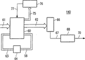
第6図は、上述の方法を実行可能な本発明によるコード装置140の実施例を示す。前記コード装置は、mビット情報語1をnビットコード語4に変換するように構成され、そして多数の異なるコード状態をsビットで示すことができる。当該コード装置は、(m+s+1)バイナリ入力信号を(n+s+t)のバイナリ出力信号に変換するコンバータ60を有する。コンバータの入力のうち、m個の入力がmビット情報語を受信するバス61に結合される。前記コンバータの出力のうち、n個の出力がnビットコード語を供給するためにバス62に結合される。更にs個の入力が、現在のコード状態を示す状態語を受信するためにsビットバス63に結合される。状態語は、例えば、s個のフリップフロップの形態のバッファメモリ64に供給される。バッファメモリ64は、当該バッファメモリに格納されるべき状態語を入力するためのバス58に結合されたs個の入力端子を有する。前記バッファメモリに記憶すべき状態語を出力するために、コンバータ60のバス58に結合されたs個の出力が使用される。
バス62は、バス62を介して受信したコード語4を、信号ライン67を介して変調回路68に供給する直列ビット列に変換するパラレル−シリアルコンバータ66のパラレル入力に結合される。前記変調回路68は、上記ビット列を、信号ライン70を介して供給される変調信号に変換する。この変調回路68は、例えば、モジュロ2積分器と呼ばれるような一般的な形式の回路であろう。
前記コード語及び状態語に加えて、前記コンバータは、
−関連する状態語に関して、前記コード語又はコード語の組が対応する情報語に割り当てられるかどうかを示し、
−これらの割り当てられたコード語の各々に対して、このコード語に対応する情報信号部の始めにおいて該変化がハイの信号値であったとした場合の、コード語により生じるデジタル合計値の変化dDSVを示し、
−前記コード語内の「1」ビットの数が偶数か奇数かを示す、
情報を、入力された情報語と状態語との各組み合わせに対してバス75に与える。
選択回路76への情報転送のために、前記バス75は前記選択回路76の入力部に結合される。前記選択回路は、変調信号部に対するランニングDSVを計算する。当該部は以前の任意の点又は合成語で始めてもよい。他の実施例において、前記DSVはこれからの部分に対し計算されてもよいが、この場合においてメモリは、コード語の可能なシーケンスを一時的に記憶するのに必要とされる。
この情報に基づいて、前記選択回路76は、与えられた情報語と共にバス62に供給すべき前記コード語がDSV値を増加しなければならないのか又は減少しなければならないのかを示す選択信号を送る。この選択信号は、信号ライン77を通って前記コンバータ60へ印加される。よって前記情報語は、第8a図のテーブルで定められた関係又は第8b図のテーブルで定められた関係に従って変換されるべきである。さらに本発明に従って、前記コンバータは第1型の異なるコード状態から選択可能であるかどうか設定する。第8図のテーブルに対し、これは87から255個の情報語及び状態1又は4に応用されてもよい。実際のコード語は第1型の他の組を形成するので、前記コンバータ60はdk制約条件に従うかどうかを確認する。dk制約条件に従う場合、他の組からの語が選択可能になる。本場合において、使用する組の選択は選択信号に基づく。
前記コンバータ60は、第8a図又は8b図に示されるコード語テーブルが当該コンバータの入力部に印加される状態語と情報語との組み合わせで決められるアドレスに記憶されるROMメモリを有してもよい。前記検出信号に応答して、メモリ位置のアドレスは第8a図のテーブルに対応するコード語で以て選択されるか、又は第8b図のテーブルに対応するコード語で以て選択される。同様のROMメモリは、第7図からのコードテーブルに対し使用されてもよい。当該メモリはxで示される‘don't care’ビットに対する位置も有する。
第6図に示される実施例において、前記状態語はメモリ60に記憶される。代わりとして、前記バス62へ出力される前記コード語から前記状態語のみをゲート回路によって取り出すことが可能である。
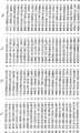
第7図は、本発明に従うコードテーブルを示す。この実施例のパラメータは、d=2,k=14,rate=8/15であり、1f(low-frequency)の内容が抑制され、エラー伝播が多くとも1バイトに制限される。更にそれは特定の20ビットのシンクパターンを持ち、エンコード及びデコードするためにテーブルを4つのみ使用する。
この実施例のためのエンコーダは、8ビット入力部、15ビット出力部及び(離散)時間関数である内部状態を有する装置である。動作原理は、従来の有限状態機械、計算分野のよく知られた理論及び自動理論により表すことができる。前記エンコーダは4つの状態でモデル化される。前記状態は端部で接続され、当該端部は順番にコード語と呼ばれるタグで分類される。この実施例における語は、前述されたdk制約条件に従う15ビットシーケンスである。4つの状態の各々は以下に示すような与えられた状態を挿入する語の型を特徴とする。
状態1に入る語は‘one’で終了し、
状態2及び3に入る語は{2,...,8}個続く‘zero’で終了し、
状態4に入る語は{1,9,...,11}個続く‘zero’で終了し、
前記状態を離れる語は、状態に入る語と状態を離れる語との連続はdk制約条件に従うやり方で選択される。例えば、状態1を離れる語は少なくとも2個の0のランレングスで始まる。状態2及び3から現れる語は上記ランレングス制約条件に従うが、当該語は他の制約条件にも従う。状態3を離れる語は、例えば、第1ビット(msb)x1及び第3ビットx3が両方とも0に等しいように選択される。同様の方法において、状態2を離れる語は、x1x3の2組が00ではないという事実を特徴とする。明らかに、状態2又は3を離れる語の組は共通の語を有さない、つまり、前記2組は分離されている。前記4個の状態の属性は、状態から状態へステップするグラフを通るどの道も前記状態を接続する前記端部にタグを付けられた語を読み取ることによりdk制約条件のシーケンスを生成することを意味する。
前記エンコーダグラフは、入力、出力及び状態という3個の組並びに出力関数H()及び次の状態関数G()という2個の論理関数の点から定義される。前記エンコーダによって瞬時tで送信されて、Xtで表される特定のコード語は、当該エンコーダに入る情報後Btの関数であるが、更に当該エンコーダの特別な状態Stにも依存する。同様に、瞬時t+1での次の状態はBtとStとの関数である。前記出力関数H()及び次の状態関数G()は、以下のように書くことができる。
Xt=H(Bt,St)
St+1=G(Bt,St)
両方の関数は、第7図に示すように256個のエントリーを持つ4つのリストで説明される。1番目の列は、0から225個の情報語を示す。2番目の列は、状態1に対するコード語を与え、3番目の列は、(1,2,3又は4で示す)次のコード状態を与える。他の列は、状態S2,S3及びS4のそれぞれを表す。前記コード状態S1及びS4は、前記EFM+の文献で記載された第1型に関する。前記コード状態S2及びS3は、第2型に関する。前記語はNRZI記号で書かれる。第7図の最初の16行において、いくつかのビットは、(don't careという意味の)「x」として与えられる。これはこのビット位置に対し0又は1を使用してもよいことを表す。2個の対の語が情報語各々に対し有効であり、当該語は一つの位置でのみ異なる。この自由度は、変調信号のLFの内容を最小にするように使用されなければならず、DC制御(DCC)としても表される。
第7図のコードテーブルにおいて、語はS1で対応する語を持つ状態S4での132から255までの情報語で対となる。前記DS制御で説明されるように、コード状態S4においてS1からの語をS4の語の代わりに選択してもよい。簡単にデコードするために、S1で対になった語は、S4の組の一部にすべきではない。もし共通の語がV1及びV4で使用される場合、同じ情報語に割り当てらるべきである。これは、設定された状態を知ることなくコード語が特定的にデコードされるという利点がある。
前記DC制御は異なる2つの方法で可能となる。1番目は、前記テーブルが出力テーブルにおいて「don't care」を示す場合、ランニングデジタル合計を最適にするためにこの程度の自由度を使用してもよい。2番目は、現在の状態がs=4であり且つ前のコード語Xt−1とのランレングス制約条件がそれを許容するかである(すなわち、Xt−1とH(Bt,1)との並列が、dk制約条件に従うか)。第7図に示される実施例において、付加的特徴は、G(Bt,1)=G(Bt,4)という制約条件によって達成される。これは、現在のコード語へ連続的に生じる同じコード語になる。DCCのために選択するコード語の決定を延期するシステムにおいて、起こり得るシーケンスのストリームは(現在のコード語で)一つの位置でのみ異なる。前記DCCユニットに対する計算及びメモリの必要性をやわらげる。エンコードシーケンスのランニングデジタル合計を最小にするもう一つのストリームが選択される。本実施例のスペクトル密度は第9図に示される。
シンクパターンは、規則的に変調信号へ加えられる。特定の及び信頼性のあるパターンの定義は、20ビットシーケンス「x0010 00000 00000 00001」である。前記シンクパターンが始まる直前、前記エンコーダはsと呼ばれるある状態になる。xで示される、シンクパターンのmsbの絶対値はsによって次のように制御される。s=2の場合、前記xは1に、さもなければx=0に設定される。前記シンクパターンの送信後、前記エンコーダは状態1にプリセットされる。
同様の制約条件下で構成された他のコードテーブルに対し、コード状態S1において、対の語をS4から使用することも可能にするであろう。しかしながら、第7図のテーブルについては、d,k制約条件に従わないので、語は使用されない。第1型のコード状態の異なる数若しくはコード語又は異なる語長m及びnの異なる割り当てに関し、異なるコードテーブルは、対の語を割り当てることによって第1型のコード状態の一つを自由に選択する自由度が前記変調信号の低周波特性を改善するのに使用されるように構成される。
第8図は、レート8/16を持つコードテーブルを示す。m=8及びn=16でdk制約条件は、d=2,k=10である。列は、第7図で組織されるが、記号xは2重の語を表すのに使用されるが、代わりとしてメイン及び代用テーブルが与えられる。第8a図はメインコードテーブルを示し、第8b図は情報語0から87に対する別れた代用テーブルを示す。前記代用テーブルのコード語は、先行技術のEFM+の文献で記載されるDC制御に対し選択されてもよい。この実施例において、状態1又は4の場合、本発明に従うコード語は第1型の他の状態、状態4又は1それぞれから選択されてもよい。更に、シンクパターンが加えられてもよい。前記シンクパターンは、例えば、k+1個の0の系列を含むことによってk制約条件に従わないことで、当該パターンを簡単に区別するために特定のパターンを持つ。シンクパターンの後、前記状態は、状態1のような所定の値にリセットされる。
第9図は、第7図のコードのコンピュータシミュレーションの結果を示す。スペクトル密度は周波数に対して計算され、当該密度は、前記ビット周波数に関するレートとして与えられる。レートコード8/15に対する良好なLFの実施は、曲線で示される。Technical field
The present invention is a method for converting a sequence of m-bit information words, where m is an integer, into a modulated signal, The information word sequence is converted into an n-bit codeword sequence in which n is an integer exceeding m in accordance with a conversion rule so that the corresponding modulation signal satisfies a predetermined criterion, and the output is output. The code word is modulated into the modulated signal, and in the converting step, The code words are distributed in at least a first type group and at least a second type group, while the output of each of the code words belonging to the first type group is determined by the corresponding group And the output of each of the code words belonging to the second type group is determined by the corresponding group and the information word corresponding to the output code word When a state is generated and one of the code words is assigned to the input information word, this code word is derived from the set of code words depending on the code state generated when the preceding code word is output. On the other hand, a set of code words belonging to the code state of the second type does not have any code word in common, and the group of the second type has at least one code word associated with a plurality of information words. Each Word is followed Code word The present invention relates to a method that can be distinguished by detection.
The present invention provides a signal obtained by the above method. Supply to record carrier Also related to the method.
The invention further relates to a coding device for carrying out the method according to the claim, the device converting an m-bit information word into an n-bit code word, and these n-bit code words. Means for converting into a modulated signal.
The invention further relates to a recording device in which a code device of this type is used.
The invention further relates to a signal.
The invention further relates to a record carrier on which the signal is recorded.
Background art
Such a method, device, record carrier and signal are known from WO 95/22802 (corresponding to European Patent Publication No. EP-A-94200387.2, PHN14746). The publication relates to a method for converting a sequence of m-bit information words into a modulated signal, said method being called EFM +. An n-bit code word is output for each information word from the sequence. The output code word is converted into a modulated signal. The code words are distributed in at least one group of the first type and at least one group of the second type. For each codeword output belonging to the first type group, the corresponding group generates a first type code state. When code words belonging to the second type group are output, the second type code state is generated. A code word is assigned to an input information word selected from a set of code words depending on the generated code state. A set of code words belonging to the second type code state is separated. A selected one of the possible second type code sets is determined by the information word corresponding to the output code word. This allows similar code words and some of the corresponding information words to be in different generated code states. In this coding method, the number of specific bit combinations used in code words in the sequence increases, thereby increasing code efficiency. The modulation signal thus obtained is first converted into a codeword sequence, then the logical value of the bits of the bit string at a predetermined position depending on and related to the codeword to be converted Alternatively, the information word may be reconverted by assigning the information word to each of the code words from the series depending on the information word. The logical value is an indication for a code state generated in advance. Furthermore, a recording device and a reading device are disclosed.
Low frequency components of the modulation signal may be prevented by other system parameters such as servo signals in the recording system. Even if the above conversion method is a modulated signal having a limited low frequency content, it is still necessary to reduce the low frequency component.
Disclosure of the invention
Therefore, an object of the present invention is to provide means for performing conversion suitable for reducing the low frequency content of the modulated signal.
According to a first aspect of the present invention, the purpose is to generate a first type code state, Depending on the low frequency content of the modulated signal while following predetermined criteria, The code word is achieved by the method described at the beginning, characterized in that it is selected from a set belonging to the generated code state or from a set depending on a different first type code state.
According to a second aspect of the present invention, this object is , This is achieved using a record carrier, a code device, a recording device and a method of manufacturing a record carrier. The measure according to the invention has the advantage that the low frequency content (sometimes called DC) of the modulated signal is reduced while keeping the same information code effect.
[Brief description of the drawings]
Hereinafter, the present invention will be described with reference to FIG. 1 to FIG.
FIG. 1 shows a sequence of information words, a corresponding sequence of code words and a modulated signal,
FIG. 2 shows a record carrier,
FIG. 3 shows an enlarged portion of the record carrier of FIG.
FIG. 4 shows a recording device,
FIG. 5 shows a decoding and playback device,
FIG. 6 shows a coding device;
7 and 8 show tables representing the relationship between information words and code words, and
FIG. 9 shows the frequency spectrum of the modulated signal.
BEST MODE FOR CARRYING OUT THE INVENTION
FIG. 1 shows three consecutive m-bit information words, in this case 8-bit information words indicated by 1. Information on the coding method can be found in the literature entitled “Cording Techniques for Digital Recorders” (ISBN 0-13-140047-9) by KA Schouhamer Immink. This document describes, for example, a so-called EFM modulation system, which is used for recording information on a so-called compact disc. The EFM modulated signal is obtained by converting a sequence of 8-bit information words into a sequence of 14-bit code words, and in this case, three extra bits are inserted between each code word. These code words are selected such that the minimum number of “0” bits between “1” bits is d (2) and the maximum number is k (10). This constraint is also called a dk constraint. The code word sequence is converted into a corresponding signal formed by a bit cell having a high or low signal value by a modulo-2 integral operation, and in this modulated signal (modulated signal), the “1” bit is changed from a high signal to a low signal. It is represented by a change to value or vice versa. On the other hand, the “0” bit is represented by no change in signal value at the transition between two bit cells. The margin bits are selected such that the dk constraint is satisfied even in the transition region between the two code words, and the so-called running digital sum is substantially constant in the corresponding signal. The running digital total value at a particular instant means the difference between the number of bit cells with a high signal value and the number of bit cells with a low signal value, calculated over the portion of the modulation signal located before that instant. To be understood. A substantially constant running digital total value means that the frequency spectrum of the signal has no frequency component in the low frequency region. Such a signal is also called a DC free signal. The absence of low frequency components in the signal is very advantageous when the signal is read from a record carrier on which the signal is recorded in the track. This is because in this case, continuous tracking control that is not affected by the recorded signal is possible. On the other hand, information recording always requires an improvement in information density on a record carrier. In FIG. 1, these three
The bit string formed by the
Furthermore, the frequency spectrum of the modulated
In the following, an embodiment of the method according to the invention for obtaining a modulated signal will be described in detail.
First of all, there is a requirement for code words that the dk constraint is satisfied. The group of all possible code words that satisfy the dk constraint condition is divided into at least a first type group and at least a second type group. When a code word is supplied from one of the first type groups, a code state that is exclusively dependent on the first type group to which the supplied code word belongs is set. When one of the code words of the first type group is supplied, the code state is set depending on both the first type group and the information word indicated by the supplied code word. In this embodiment, two groups of the first type, for example, a first group G11 having code words ending with a bit (a is 0 or 1) having a logical value “0”, and a logical value “0”. Can be distinguished from the second group of code words G12 ending with b bits (where b is an integer not less than 9 and not less than 6).
The code state set by the first group G11 of the first type is hereinafter referred to by the reference symbol S1. The code state set by the first type second group G12 is hereinafter referred to by reference numeral S4. The embodiment described here knows only one second type group. This group includes code words that end with c bits having a logical value “0” (c is an integer of 2 to 5). This group will hereinafter be referred to as group G2. In the embodiment described here, two code states, for example S2 and S3, can be set by a combination of a code word and a corresponding information word.
When an information word is converted into a code word, a code word belonging to a group of code words depending on the code state is assigned to the information word to be converted. The group of codewords belonging to the code states S1, S2, S3, S4 is hereinafter referred to by the reference signs V1, V2, V3, V4, respectively. The code words of the group are selected so that each bit string that can be formed by a code word from the group for which the code state is set and an arbitrary code word from the group for which the code state is set satisfies the dk constraint condition Is done. If the code state S4 is set by supplying the previously supplied code word, and this code state indicates that the preceding code word ends with an a bit string having a logical value “0” of 6 or more and 9 or less, the code state The code word group V4 set by S4 is only allowed to have a code word having a logical value “0” and starting with a maximum of 1 bit. Because of this, a code word starting with a number of bits having a logical value “0” will have a transition region between the code word supplied earlier and the code word to be supplied. In this region, the number of consecutive bits having a logical value “0” is not always less than 10 and therefore does not satisfy the dk constraint condition. For the same reason, the set V1 has only code words that start with a large number of bits having a logical value “0” of 2 to 9.
The code word sets V2 and V3 belonging to the code states S2 and S3 include only code words starting with a number of bits having a logical value “0” of 0 or more and 5 or less. Code words that satisfy this state are distributed into two sets V2, V3, so that the sets V2, V3 do not contain any common code words. The sets V2, V3 will be referred to as separate sets in the following. The distribution of the code words in the sets V2 and V3 is preferably such that the code word can belong to which set based on a limited number of logical values of p bits. In the above example, bit combination x1. x13 is used for this purpose. The code words from set V2 are bit combined x1. It can be recognized from x13 = 0.0. The code words from set V3 are combined x1. It can be recognized from x13. Code words that set the code state S1 (group G11) during supply, code words that set the code states S2 and S3 (group G2) during supply, and code words that set the code state S4 (group G12) during supply A distinction is made between Set V1 has 138 code words from group G11, 96 code words from group G2, and 22 code words from group G12. It will be demonstrated that the number of different code words in set V1 is less than the number of different 8-bit information words.
The code word from the group G2 is always followed by the code word from the set V2 or the code word from the set V3, and further, where the code word is based on the code word following the code word from the group G2. Since a code word from group G2 followed by a code word from set V2 is the same code word from group G2 but is followed by a code word from set V3 It can be clearly distinguished. In other words, when a code word is assigned to an information word, each code word from group G2 can be used twice. Each code word from group G2 forms a unique bit combination that cannot be separated from the bit combination formed by the random code word from set V2 and the random code word from the same set V3. This includes 138 unique bit combinations (codewords) from group G11, 22 unique bit combinations (codewords) from group G12, and 2 × 96 unique bit combinations from group G2. Means that the code word from group G2 combined with the following code word can be used for set V1. This combination provides a total number of 352 usable unique bit combinations. The numbers of unique bit combinations formed by codewords from the sets V2, V3, V4 are 352, 351 and 415, respectively.
FIG. 2 shows an example of a
FIG. 4 shows a recording device for recording information. For example, a code device according to the present invention such as the
FIG. 5 shows a reading device, for example a decoding device according to the invention such as a
An embodiment of the
B t = H -1 (X t -1, X t , X t +1. x1, X t +1. x3)
Preceding code word X t Note that nine observations of −1 tail bits are sufficient. From the above, error propagation is limited to at most 1 byte. A logical array that converts (9 + 15 + 2) channel bits into 8 user bits can be easily reduced by taking advantage of the slight characteristics of the code. The
FIG. 6 shows an embodiment of a
The
In addition to the code word and the status word, the converter
-For an associated status word, indicating whether said code word or set of code words is assigned to a corresponding information word;
For each of these assigned codewords, the change in the digital total value dDSV caused by the codeword if the change was a high signal value at the beginning of the information signal part corresponding to this codeword Indicate
-Indicates whether the number of "1" bits in the code word is even or odd;
Information is provided to the
The
Based on this information, the
The
In the embodiment shown in FIG. 6, the state word is stored in the
FIG. 7 shows a code table according to the present invention. The parameters of this embodiment are d = 2, k = 14, rate = 8/15, the content of 1f (low-frequency) is suppressed, and error propagation is limited to at most 1 byte. Furthermore, it has a specific 20-bit sync pattern and uses only four tables for encoding and decoding.
The encoder for this embodiment is a device having an 8-bit input, a 15-bit output, and an internal state that is a (discrete) time function. The principle of operation can be expressed by conventional finite state machines, well-known theories in the computational field and automatic theories. The encoder is modeled in four states. The states are connected at the ends, and the ends are sequentially classified by tags called code words. The term in this example is a 15-bit sequence subject to the dk constraint described above. Each of the four states is characterized by a word type that inserts a given state as shown below.
A word that enters
The words that enter states 2 and 3 are {2,. . . , 8} In a series of 'zero' Exit
The words that enter
The words leaving the state are selected in a manner that follows the dk constraint, with the sequence of words entering the state and leaving the state. For example, a
The encoder graph is defined in terms of three sets of input, output, and state, and two logical functions, output function H () and next state function G (). Transmitted at the instant t by the encoder, X t The specific code word represented by t And a special state S of the encoder t Also depends on. Similarly, the next state at instant t + 1 is B t And S t And a function. The output function H () and the next state function G () can be written as follows:
X t = H (B t , S t )
S t + 1 = G (B t , S t )
Both functions are described in four lists with 256 entries as shown in FIG. The first column shows 0 to 225 information words. The second column gives the code word for
In the code table of FIG. 7, words are paired with
The DC control is possible in two different ways. First, if the table shows “don't care” in the output table, this degree of freedom may be used to optimize the running digital sum. Second, the current state is s = 4 and the previous code word X t Whether the run length constraint with −1 allows it (ie, X t -1 and H (B t , 1) follows the dk constraint) In the embodiment shown in FIG. 7, the additional feature is G (B t , 1) = G (B t , 4). This will be the same code word that occurs continuously to the current code word. In a system that defers the determination of the codeword to select for DCC, the possible sequence streams differ (at the current codeword) only at one location. Alleviates the computational and memory requirements for the DCC unit. Another stream is selected that minimizes the running digital sum of the encoding sequence. The spectral density of this example is shown in FIG.
The sync pattern is regularly added to the modulation signal. The definition of a specific and reliable pattern is the 20-bit sequence “
For other code tables configured under similar constraints, it would also be possible to use pair words from S4 in code state S1. However, in the table of FIG. 7, the word is not used because it does not follow the d, k constraint. For different numbers or code words of
FIG. 8 shows a code table having a rate of 8/16. For m = 8 and n = 16, the dk constraints are d = 2 and k = 10. The columns are organized in FIG. 7, but the symbol x is used to represent double words, but instead main and substitution tables are given. FIG. 8a shows the main code table, and FIG. 8b shows a separate substitution table for
FIG. 9 shows the result of computer simulation of the code of FIG. Spectral density is calculated over frequency, and the density is given as a rate for the bit frequency. A good LF implementation for
Claims (10)
Applications Claiming Priority (3)
| Application Number | Priority Date | Filing Date | Title |
|---|---|---|---|
| EP95202367 | 1995-09-01 | ||
| AT95202367.9 | 1995-09-01 | ||
| PCT/IB1996/000858 WO1997009718A1 (en) | 1995-09-01 | 1996-08-26 | Method of converting a series of m-bit information words to a modulated signal, method of producing a record carrier, coding device, device, recording device, signal, as well as a record carrier |
Related Child Applications (1)
| Application Number | Title | Priority Date | Filing Date |
|---|---|---|---|
| JP2005276620A Division JP3946230B2 (en) | 1995-09-01 | 2005-09-22 | Record carrier |
Publications (2)
| Publication Number | Publication Date |
|---|---|
| JPH10508456A JPH10508456A (en) | 1998-08-18 |
| JP3754080B2 true JP3754080B2 (en) | 2006-03-08 |
Family
ID=8220604
Family Applications (2)
| Application Number | Title | Priority Date | Filing Date |
|---|---|---|---|
| JP51101997A Expired - Lifetime JP3754080B2 (en) | 1995-09-01 | 1996-08-26 | Method, code device, and recording device for converting m-bit information word sequence into modulation signal |
| JP2005276620A Expired - Lifetime JP3946230B2 (en) | 1995-09-01 | 2005-09-22 | Record carrier |
Family Applications After (1)
| Application Number | Title | Priority Date | Filing Date |
|---|---|---|---|
| JP2005276620A Expired - Lifetime JP3946230B2 (en) | 1995-09-01 | 2005-09-22 | Record carrier |
Country Status (23)
| Country | Link |
|---|---|
| US (1) | US5790056A (en) |
| EP (1) | EP0789910B1 (en) |
| JP (2) | JP3754080B2 (en) |
| KR (1) | KR100488634B1 (en) |
| CN (3) | CN1909097B (en) |
| AT (1) | ATE201527T1 (en) |
| AU (1) | AU703791B2 (en) |
| CA (1) | CA2205565C (en) |
| DE (2) | DE69612955T4 (en) |
| ES (1) | ES2159040T4 (en) |
| GR (1) | GR3036397T3 (en) |
| HK (1) | HK1004699A1 (en) |
| HU (1) | HU221391B1 (en) |
| ID (1) | ID16164A (en) |
| IL (1) | IL120740A (en) |
| MX (1) | MX9703161A (en) |
| MY (1) | MY115841A (en) |
| PL (1) | PL183099B1 (en) |
| PT (1) | PT789910E (en) |
| RU (1) | RU2153200C2 (en) |
| TW (1) | TW394931B (en) |
| WO (1) | WO1997009718A1 (en) |
| ZA (1) | ZA967261B (en) |
Families Citing this family (24)
| Publication number | Priority date | Publication date | Assignee | Title |
|---|---|---|---|---|
| KR100644599B1 (en) * | 2000-09-06 | 2006-11-13 | 삼성전자주식회사 | Method of modulation and/or demodulation of RLL code having enhanced DC suppression capability |
| TW362305B (en) * | 1996-10-18 | 1999-06-21 | Koninkl Philips Electronics Nv | Apparatus and method for converting a sequence of m-bit information words into a modulated signal |
| US6297753B1 (en) * | 1999-01-29 | 2001-10-02 | Victor Company Of Japan, Ltd. | Eight-to-fifteen modulation using no merging bit and optical disc recording or reading systems based thereon |
| KR100294893B1 (en) * | 1999-03-09 | 2001-07-12 | 윤종용 | Method for generating RLL code having enhanced DC suppression capability, and modulation method and demodulation method of the generated RLL code |
| KR100565046B1 (en) * | 1999-04-21 | 2006-03-30 | 삼성전자주식회사 | Method of arranging RLL code having enhanced DC suppression capability, modulation method, demodulation method and demodulation apparatus therefor |
| TW538372B (en) * | 1999-10-02 | 2003-06-21 | Mediatek Inc | Zero digital sum value control device and method |
| US6967597B1 (en) | 2000-11-08 | 2005-11-22 | Lg Electronics, Inc. | Method and apparatus for coding information, method and apparatus for decoding information, method of fabricating a recording medium, the recording medium and modulated signal |
| EA003569B1 (en) * | 2000-05-10 | 2003-06-26 | Конинклейке Филипс Электроникс Н.В. | Method of converting a stream of databits of a binary information signal into a stream of databits of a constrained binary channel signal, a device for encoding, signal comprising a stream of databits of a constrained binary channel signal, record carrier, method for decoding, device for decoding |
| KR20020038709A (en) * | 2000-06-02 | 2002-05-23 | 요트.게.아. 롤페즈 | Device for encoding a stream of databits of a binary source signal into a stream of databits of a binary channel signal, memory means, device for recording information, record carrier, device for coding and device for playing back |
| KR100424482B1 (en) * | 2000-06-22 | 2004-03-24 | 엘지전자 주식회사 | Method and apparatus of converting a series of data words into a modulated signal |
| JP3709818B2 (en) | 2000-10-31 | 2005-10-26 | 日本ビクター株式会社 | ENCODING TABLE AND MODULATION DEVICE, TRANSMISSION DEVICE, AND RECORDING MEDIUM USING THE SAME |
| JP3664091B2 (en) * | 2001-01-12 | 2005-06-22 | 日本ビクター株式会社 | Modulation method, modulation device, demodulation method, demodulation device, method of recording on information recording medium, information transmission method and information transmission device |
| US6853320B2 (en) * | 2001-01-16 | 2005-02-08 | Victor Company Of Japan, Ltd. | Modulation system |
| JP2002304859A (en) * | 2001-02-02 | 2002-10-18 | Victor Co Of Japan Ltd | Synchronous signal generating method, recording apparatus, transmitting apparatus, recording medium, and transmission medium |
| KR100669623B1 (en) * | 2001-03-12 | 2007-01-15 | 엘지전자 주식회사 | Converting method of digital data |
| KR100725685B1 (en) * | 2001-07-05 | 2007-06-07 | 엘지전자 주식회사 | Method of converting a series of data words into a modulated signal |
| KR100470026B1 (en) * | 2001-07-05 | 2005-02-04 | 엘지전자 주식회사 | Method and apparatus for coding/decoding information |
| WO2003023971A2 (en) * | 2001-09-10 | 2003-03-20 | Koda Investments Limited | Coding method and device |
| CN100477529C (en) * | 2002-01-23 | 2009-04-08 | 皇家飞利浦电子股份有限公司 | Method for converting information words to a signal, coder and reproducer thereof |
| JP4143330B2 (en) * | 2002-05-14 | 2008-09-03 | ソニー株式会社 | Data recording medium, data recording method and apparatus |
| US7378994B1 (en) * | 2007-01-08 | 2008-05-27 | Mediatek, Inc. | EFM/EFM+ encoder and method thereof |
| JP4521458B2 (en) * | 2008-12-11 | 2010-08-11 | 株式会社東芝 | Run length limiting device and run length limiting method |
| JP6715053B2 (en) * | 2016-03-26 | 2020-07-01 | 三井精機工業株式会社 | Chatter control method for machine tools |
| WO2019209246A1 (en) * | 2018-04-23 | 2019-10-31 | Hewlett-Packard Development Company, L.P. | Reflection and inversion invariant codes |
Family Cites Families (4)
| Publication number | Priority date | Publication date | Assignee | Title |
|---|---|---|---|---|
| DE68920739T2 (en) * | 1989-08-16 | 1995-06-29 | Ibm | Data coding for the immediate start of PRML receivers. |
| JP2741112B2 (en) * | 1991-03-29 | 1998-04-15 | シャープ株式会社 | Digital modulation method and digital modulation device |
| DE69227795T2 (en) * | 1991-03-30 | 1999-05-27 | Toshiba Kawasaki Kk | Encoder for digital signals with improved channel block coding |
| DE69505794T2 (en) * | 1994-02-15 | 1999-06-02 | Koninkl Philips Electronics Nv | METHOD FOR CONVERTING M-BIT INFORMATION WORDS INTO A MODULATED SIGNAL, METHOD FOR PRODUCING A RECORDING CARRIER, ENCODING, DECODING, RECORDING AND READING DEVICE AND RECORDING CARRIER |
-
1996
- 1996-08-26 HU HU9801354A patent/HU221391B1/en unknown
- 1996-08-26 CN CN2006101016657A patent/CN1909097B/en not_active Expired - Lifetime
- 1996-08-26 CN CNB961912448A patent/CN1145955C/en not_active Expired - Lifetime
- 1996-08-26 JP JP51101997A patent/JP3754080B2/en not_active Expired - Lifetime
- 1996-08-26 PT PT96926545T patent/PT789910E/en unknown
- 1996-08-26 DE DE69612955T patent/DE69612955T4/en not_active Expired - Lifetime
- 1996-08-26 AU AU66667/96A patent/AU703791B2/en not_active Expired
- 1996-08-26 CN CNB021604746A patent/CN1331148C/en not_active Expired - Lifetime
- 1996-08-26 RU RU97108582/28A patent/RU2153200C2/en active
- 1996-08-26 EP EP96926545A patent/EP0789910B1/en not_active Expired - Lifetime
- 1996-08-26 MX MX9703161A patent/MX9703161A/en unknown
- 1996-08-26 PL PL96320006A patent/PL183099B1/en unknown
- 1996-08-26 WO PCT/IB1996/000858 patent/WO1997009718A1/en active IP Right Grant
- 1996-08-26 ES ES96926545T patent/ES2159040T4/en not_active Expired - Lifetime
- 1996-08-26 CA CA002205565A patent/CA2205565C/en not_active Expired - Lifetime
- 1996-08-26 KR KR1019970702860A patent/KR100488634B1/en not_active IP Right Cessation
- 1996-08-26 AT AT96926545T patent/ATE201527T1/en active
- 1996-08-26 DE DE69612955A patent/DE69612955D1/en not_active Expired - Lifetime
- 1996-08-26 IL IL12074096A patent/IL120740A/en not_active IP Right Cessation
- 1996-08-27 ZA ZA9607261A patent/ZA967261B/en unknown
- 1996-08-29 MY MYPI96003603A patent/MY115841A/en unknown
- 1996-08-30 US US08/706,048 patent/US5790056A/en not_active Expired - Lifetime
- 1996-09-02 ID IDP962496A patent/ID16164A/en unknown
- 1996-10-02 TW TW085112032A patent/TW394931B/en not_active IP Right Cessation
-
1998
- 1998-05-08 HK HK98103966A patent/HK1004699A1/en not_active IP Right Cessation
-
2001
- 2001-08-16 GR GR20010401253T patent/GR3036397T3/en unknown
-
2005
- 2005-09-22 JP JP2005276620A patent/JP3946230B2/en not_active Expired - Lifetime
Also Published As
Similar Documents
| Publication | Publication Date | Title |
|---|---|---|
| JP3946230B2 (en) | Record carrier | |
| JP3892020B2 (en) | Method for converting m-bit information word sequence to modulation signal, method for manufacturing record carrier, encoding device, decoding device, and method for converting modulation signal to m-bit information word sequence | |
| US5748119A (en) | Devices and methods for channel-encoding and channel-decoding of digital data | |
| EP0971355B1 (en) | Record medium storing a signal | |
| US6664905B1 (en) | Device for encoding n-bit source words into corresponding m-bit channel words and decoding m-bit channel words into corresponding n-bit source words | |
| JPH0652620B2 (en) | Code converter, recording medium, and data conversion method | |
| US7119721B2 (en) | Converting information words into different length code words depending on a property of a code signal | |
| JP3722331B2 (en) | Modulation apparatus and method, and recording medium | |
| US5870037A (en) | Method and apparatus, demodulating method and signal demodulating apparatus | |
| US6768432B2 (en) | Method of converting a series of m-bit information words into a modulated signal | |
| US5969651A (en) | Signal modulating method, signal modulating apparatus, signal demodulating method and signal demodulating apparatus | |
| KR100945183B1 (en) | System of converting information words to a signal | |
| JP2005502980A (en) | Encoding method and apparatus | |
| IL127149A (en) | Digital signal modulation method and apparatus | |
| JPH01191522A (en) | 4/7 nrzi code conversion system |
Legal Events
| Date | Code | Title | Description |
|---|---|---|---|
| A131 | Notification of reasons for refusal |
Free format text: JAPANESE INTERMEDIATE CODE: A131 Effective date: 20050322 |
|
| RD04 | Notification of resignation of power of attorney |
Free format text: JAPANESE INTERMEDIATE CODE: A7424 Effective date: 20050408 |
|
| A601 | Written request for extension of time |
Free format text: JAPANESE INTERMEDIATE CODE: A601 Effective date: 20050621 |
|
| A602 | Written permission of extension of time |
Free format text: JAPANESE INTERMEDIATE CODE: A602 Effective date: 20050808 |
|
| A524 | Written submission of copy of amendment under article 19 pct |
Free format text: JAPANESE INTERMEDIATE CODE: A524 Effective date: 20050922 |
|
| TRDD | Decision of grant or rejection written | ||
| A01 | Written decision to grant a patent or to grant a registration (utility model) |
Free format text: JAPANESE INTERMEDIATE CODE: A01 Effective date: 20051115 |
|
| A61 | First payment of annual fees (during grant procedure) |
Free format text: JAPANESE INTERMEDIATE CODE: A61 Effective date: 20051215 |
|
| R150 | Certificate of patent or registration of utility model |
Free format text: JAPANESE INTERMEDIATE CODE: R150 |
|
| FPAY | Renewal fee payment (event date is renewal date of database) |
Free format text: PAYMENT UNTIL: 20081222 Year of fee payment: 3 |
|
| FPAY | Renewal fee payment (event date is renewal date of database) |
Free format text: PAYMENT UNTIL: 20091222 Year of fee payment: 4 |
|
| FPAY | Renewal fee payment (event date is renewal date of database) |
Free format text: PAYMENT UNTIL: 20101222 Year of fee payment: 5 |
|
| FPAY | Renewal fee payment (event date is renewal date of database) |
Free format text: PAYMENT UNTIL: 20111222 Year of fee payment: 6 |
|
| FPAY | Renewal fee payment (event date is renewal date of database) |
Free format text: PAYMENT UNTIL: 20121222 Year of fee payment: 7 |
|
| FPAY | Renewal fee payment (event date is renewal date of database) |
Free format text: PAYMENT UNTIL: 20131222 Year of fee payment: 8 |
|
| R250 | Receipt of annual fees |
Free format text: JAPANESE INTERMEDIATE CODE: R250 |
|
| R250 | Receipt of annual fees |
Free format text: JAPANESE INTERMEDIATE CODE: R250 |
|
| R250 | Receipt of annual fees |
Free format text: JAPANESE INTERMEDIATE CODE: R250 |
|
| EXPY | Cancellation because of completion of term |