JP3748343B2 - Switching control device, switching device, and vehicle power supply device - Google Patents
Switching control device, switching device, and vehicle power supply device Download PDFInfo
- Publication number
- JP3748343B2 JP3748343B2 JP28823299A JP28823299A JP3748343B2 JP 3748343 B2 JP3748343 B2 JP 3748343B2 JP 28823299 A JP28823299 A JP 28823299A JP 28823299 A JP28823299 A JP 28823299A JP 3748343 B2 JP3748343 B2 JP 3748343B2
- Authority
- JP
- Japan
- Prior art keywords
- voltage
- terminal
- load
- power supply
- drive voltage
- Prior art date
- Legal status (The legal status is an assumption and is not a legal conclusion. Google has not performed a legal analysis and makes no representation as to the accuracy of the status listed.)
- Expired - Fee Related
Links
Images


Landscapes
- Control Of Voltage And Current In General (AREA)
- Power Conversion In General (AREA)
Description
【0001】
【発明の属する技術分野】
本発明は、スイッチング制御装置、スイッチング装置及び車両用電源供給装置に係わり、特に、車載バッテリから負荷への電源供給をオンオフする3端子スイッチング素子を制御するスイッチング制御装置、前記スイッチング制御装置と3端子スイッチング素子とを備えたスイッチング装置及び、車両に搭載された負荷と、該負荷に電源を供給する車載バッテリと、前記スイッチング装置を備えた車両用電源供給装置に関する。
【0002】
【従来の技術】
従来、車両においては、ライトスイッチ、オーディオスイッチ等の操作スイッチの操作に応じて車載バッテリからの電源を選択的に各負荷に供給するために、車載バッテリと各負荷との間にそれぞれ機械式リレーを設けられている。そして、操作スイッチのオン操作により、該操作スイッチに応じた機械式リレーがオンして選択的に車載バッテリからの電源が負荷に供給される。近年では、半導体製造技術の進歩に伴って、性能が良くかつ安価な半導体スイッチ素子が容易に手に入るようになったため、上述した機械式リレーに代えて半導体スイッチ素子を用いたものが提案されている。
【0003】
ところで、車両において、車載バッテリからの電源は半導体スイッチ素子及び絶縁被膜により被われた電源線を介して車両の各部に配されている負荷に供給されている。上述した電源線は、常時振動しているエンジンルーム内等において車体に沿って配索されるが、このとき、車体の各部に接近して位置されていると、振動により角部と断続的な接触を繰り返すようになり、これが長期間続くと電源線の被覆が車体の角部により徐々に削られて内部導線が微少ではあるが露出するようになる。
【0004】
この電源線の露出部が車体と接触することに伴って、電源線にデッドショートやレアショートが起こり、過電流が流れると半導体スイッチ素子や電源線が過熱して熱破壊する事態に至るようになる。そこで、このような事態に至ることを未然に防止するために、従来、半導体スイッチング素子と、該半導体スイッチ素子を過電流や過熱から保護するためのスイッチング制御装置とを有したインテリジェントパワースイッチと呼ばれるスイッチング装置が提案されている。このようなスイッチング装置の一例として具体的には図2に示されるようなものが知られている。
【0005】
図2は、スイッチング制御装置及びスイッチング装置を組み込んだ車両用電源供給装置を示す回路図である。同図において、車載バッテリ1からの電源電圧VBは、パワーMOSFETQF(3端子スイッチング素子)のドレインD(電源側端子)−ソースS(負荷側端子)間を介して負荷3に対して供給される。上述したパワーMOSFETQFは、そのゲートTG(制御端子)が駆動回路DRに接続されており、該駆動回路DRから駆動電圧VPが供給されるとドレインD―ソースS間を導通して電源電圧VBを負荷3に対して供給する。
【0006】
また、パワーMOSFETQFのドレインD、ソースSは差動増幅器62の+、−入力端にそれぞれ接続されており、差動増幅器62はパワーMOSFETQFのドレインD−ソースS間の電圧VDSをコンパレータCP3の−入力端に対して出力する。従って、+入力端に電源電圧VBを抵抗R6及びR7で分圧した基準電圧Vref4が供給されているコンパレータCP3は、差動増幅器62の出力電圧VDSが基準電圧Vref4を越えるとLレベルの過熱検出信号S6をANDゲート63の一端に対して出力する。
【0007】
このANDゲート63の他端には、一端が抵抗R1を介してアースと接続され、他端が電源電圧VBに接続されている外付けの操作スイッチSWの一端が接続され、操作スイッチSWがオン操作されるとHレベルのオン操作信号S2が供給される。そして、ANDゲート63はオン操作信号S2の出力に応じて駆動回路DRに対してオン制御信号S5を出力し、また、オン操作信号S2の出力中にLレベルの過熱検出信号S6が出力されるとオン制御信号S5の出力を停止する。
【0008】
上述した駆動回路DRは、ANDゲート63からのオン制御信号S5の出力に応じて昇圧回路61により電源電圧VBを昇圧した駆動電圧VP(=VB+10[V])をゲートTGに対して出力し、パワーMOSFETQFをオンする。一方、駆動回路DRは、ANDゲート63からのオン制御信号S5の出力停止に応じてゲートTGに対する駆動電圧VPの印加を停止し、パワーMOSFETQFをオフする。
【0009】
一方、Lレベルの過熱検出信号S6は、インバータINV2を介してスイッチング(SW)トランジスタTr5のベースに対しても供給される。このSWトランジスタTr5は、コレクタがLED7を介して電源電圧VBに、エミッタがアースに接続され、Lレベルの過熱検出信号S6が出力されるとベースに接続されたインバータINV2の出力がHレベルになるため、オンしてLED7を点灯させる。なお、上述した昇圧回路61、差動増幅器62、ANDゲート63、駆動回路DR、パワーMOSFETQF、コンパレータCP3及び抵抗R6、R7は、スイッチング装置6を構成する。
【0010】
ところで、パワーMOSFETQFに流れる電流をIL、ドレインD−ソースS間の抵抗温度係数をα(>0)、パワーMOSFETQFの基準温度からの温度上昇をΔt、基準温度におけるドレインD―ソースS間の抵抗値をRとすると、このパワーMOSFETQFのドレインD−ソースS間電圧VDSは下記の式(1)で表される。
VDS=IL・(1+α・Δt)・R ……(1)
この式(1)から明らかなように電圧VDSは、パワーMOSFETQFの温度の増加に伴って増加する。
【0011】
上述した電圧VDSと電流ILとパワーMOSFETQFの温度との関係を踏まえて、上記構成のスイッチング制御装置及びスイッチング装置を組み込んだ車両用電源供給装置の動作について以下説明する。
【0012】
まず、操作スイッチSWのオン操作によりオン操作信号S2がANDゲート63に対して出力される。このとき、パワーMOSFETの温度が低ければ差動増幅器62から出力される電圧VDSは基準電圧Vref4を越えることはなく、コンパレータCP3はHレベルの出力をANDゲート63に対して出力する。従って、ANDゲート63はHレベルのオン制御信号S5を駆動回路DRに対して出力し、駆動回路DRはこのオン制御信号S5の出力により昇圧回路61からの駆動電圧VPをパワーMOSFETQFのゲートTGに対して出力する。この駆動電圧VPの出力によりパワーMOSFETQFは、オンして負荷3に対して電源電圧VBを供給する。
【0013】
一方、オン操作信号S2の出力中、パワーMOSFETQFの温度が上昇すると差動増幅器62の出力である電圧VDSは上述した式(1)に従って増加し、基準電圧Vref4を越えるとコンパレータCP3はLレベルの過熱検出信号S6を出力する。このLレベルの過熱検出信号S6の出力により、ANDゲート63は駆動回路DRに対するHレベルのオン制御信号S5の出力を停止し、駆動回路DRはオン制御信号S5の出力停止に応じてゲートTGに対する駆動電圧VPの出力を停止して、パワーMOSFETQFをオフする。従って、パワーMOSFEQFの温度が上昇して破壊に至る前に、パワーMOSFETQFに供給される車載バッテリ1からの電源電圧VBが遮断されるので、パワーMOSFETQFの熱破壊を防止することができる。
【0014】
また、Lレベルの過熱検出信号S6が出力されると、インバータINV2の出力がHレベルになり、SWトランジスタTr5がオンしてLED7を点灯させる。このLED7の点灯により、パワーMOSFETQFの過熱により負荷3へ供給される電流ILが遮断される旨を伝えることができる。
【0015】
【発明が解決しようとする課題】
ところで、一般に上述したパワーMOSFETQFは、図3に示すようなドレインD−ソースS間電圧VDS対ゲートTG−ソースS間電圧VGS特性を有する。なお、図3はゲートTG−ソースS間に4[V]の電圧が印加されたとき、ドレインD−ソースS間が完全に導通してオン駆動するTEMPFETの特性である。同図に示すように、TEMPFETのドレインD−ソースSに流れる電流IDが一定のとき、電圧VDSは電圧VGSの減少に応じて増加し、特に電圧VGSが4[V]以下に減少すると急激に増加する。すなわち、パワーMOSFETQFのVDSは、電流IDが一定のとき電圧VGSが所定電圧以下に減少すると急激に増加する。これは、パワーMOSFETQFのドレインD−ソースS間抵抗が電圧VGSの減少に伴って増加ためである。従って、昇圧回路61からの駆動電圧VPが何らかの原因で低下し、通常より低い駆動電圧VPがパワーMOSFETQFに対して出力されると電圧VGSが低下することに伴って、電圧VDSが増加してパワーMOSFETQFでの熱損失が増大する。
【0016】
しかしながら、上述した従来のスイッチング制御装置及びスイッチング装置を組み込んだ車両用電源供給装置は、電圧VDSを監視しているため実際にパワーMOSFETQFのドレインD−ソースS間に電流が流れてないと電圧VDSを検出することができない。つまり、実際にパワーMOSFETQFの熱損失が正常時に比べて増加した結果、電圧VDSが基準電圧Vref4を越えた後、初めて遮断される。
【0018】
そこで、本発明は、上記のような問題点に着目し、制御端子−負荷側端子間電圧の低下による3端子スイッチング素子の発熱を未然に防止することができるスイッチング制御装置、制御端子−負荷側端子間電圧の低下により3端子スイッチング素子が発熱することがないスイッチング装置及び、制御端子−負荷側端子間電圧の低下により3端子スイッチング素子が発熱することがない車両用電源供給装置を提供することを課題とする。
【0019】
【課題を解決するための手段】
上記課題を解決するためになされた請求項1記載の発明は、車載バッテリが接続される電源側端子、負荷が接続される負荷側端子及び駆動電圧が印加される制御端子を有する3端子スイッチング素子のオンオフ制御を行うスイッチング制御装置であって、前記制御端子への印加により前記電源側端子−前記負荷側端子間を導通させて前記3端子スイッチング素子をオンする駆動電圧を、前記車載バッテリからの電源電圧を昇圧して発生する駆動電圧発生手段と、前記3端子スイッチング素子がオンしたときの前記制御端子−前記負荷側端子間電圧を決定する電圧を検出する電圧検出手段と、負荷オン信号に応じて前記制御端子に対して前記駆動電圧を印加させ、前記電圧検出手段により検出された前記電圧が所定値以下のとき、前記負荷オン信号が存在しても前記制御端子に対する前記駆動電圧の印加を停止させる駆動電圧印加制御手段とを備えることを特徴とするスイッチング制御装置に存する。
【0020】
請求項1記載の発明によれば、駆動電圧発生手段が制御端子への印加により電源側端子−負荷側端子を導通させて3端子スイッチング素子をオンする駆動電圧を、車載バッテリからの電源電圧を昇圧して発生し、電圧検出手段が、3端子スイッチング素子がオンしたときの制御端子−負荷側端子間電圧を決定する電圧を検出し、駆動電圧印加制御手段が負荷オン信号に応じて制御端子に対して駆動電圧を印加させ、電圧検出手段により検出された電圧が所定値以下のとき、負荷オン信号が存在しても制御端子に対する駆動電圧の印加を停止させる。
【0021】
ところで、駆動電圧発生手段により発生する駆動電圧の低下に伴って、制御端子及び負荷側端子間電圧が低下すると、電源側端子−負荷側端子間電圧が増加するため、3端子スイッチング素子での熱損失が増大する。この熱損失の増大により発熱する結果、3端子スイッチング素子が熱破壊に至る恐れがあるが、3端子スイッチング素子がオンしたときの制御端子−負荷側端子間電圧を決定する電圧が所定値以下のとき、負荷オン信号が存在しても制御端子に対する駆動電圧の印加を停止させることにより、制御端子−負荷側端子間に所定値により定まる値以下の電圧が印加されることがない。
【0022】
請求項2記載の発明は、前記電圧検出手段は、前記駆動電圧発生手段により発生した前記駆動電圧と前記車載バッテリからの電源電圧との差を、前記3端子スイッチング素子がオンしたときの前記制御端子−前記負荷側端子間電圧を決定する電圧として検出し、前記駆動電圧印加制御手段は、前記電圧検出手段により検出された前記駆動電圧と前記車載バッテリからの電源電圧との差が前記所定値以下のとき、前記負荷オン信号が存在しても前記制御端子に対する前記駆動電圧の印加を停止することを特徴とする請求項1記載のスイッチング制御装置に存する。
【0023】
請求項2記載の発明によれば、電圧検出手段が駆動電圧発生手段により発生した駆動電圧と車載バッテリからの電源電圧との差を、3端子スイッチング素子がオンしたときの制御端子−負荷側端子間電圧を決定する電圧として検出し、駆動電圧印加制御手段が駆動電圧と電源電圧との差が所定値以下のとき、負荷オン信号が存在しても制御端子に対する駆動電圧の印加を停止する。
【0024】
3端子スイッチング素子がオンのとき、電源側端子−負荷側端子間電圧は極めて小さく、負荷側端子の電圧は電源電圧に等しくなる。このため3端子スイッチング素子がオンしたとき制御端子−負荷側端子に印加される電圧は、駆動電圧と電源電圧との差と等しくなる。従って、駆動電圧と電源電圧との差を、3端子スイッチング素子がオンしたときの制御端子−負荷側端子間電圧を決定する電圧とすることにより、電源電圧の減少により駆動電圧が低下しても、3端子スイッチング素子がオンしたとき、制御端子−負荷側端子間に所定値以下の電圧が印加されることがない。しかも、駆動電圧と電源電圧との差を制御端子−負荷側端子間電圧として検出することにより、単一の駆動電圧発生手段が発生した駆動電圧により、複数の3端子スイッチング素子のオンオフを行っている場合であっても、それぞれの3端子スイッチング素子ごとに電圧検出手段及び駆動電圧印加制御手段を設ける必要がない。
【0025】
請求項3記載の発明は、車載バッテリが接続される電源側端子、負荷が接続される負荷側端子及び駆動電圧が印加される制御端子を有する3端子スイッチング素子と、請求項1又は2記載のスイッチング制御装置とを備えることを特徴とするスイッチング装置に存する。
【0026】
請求項3記載の発明によれば、駆動電圧印加制御手段が負荷オン信号に応じて制御端子に対して駆動電圧を印加させ、電圧検出手段により検出された電圧が所定値以下のとき、負荷オン信号が存在しても制御端子に対する駆動電圧の印加を停止させるので、制御端子−負荷側端子間に所定値により定まる値以下の電圧が印加されることがない。
【0027】
請求項4記載の発明は、車両に搭載された負荷と、該負荷に電源を供給するための車載バッテリと、車載バッテリが接続される電源側端子、負荷が接続される負荷側端子及び駆動電圧が印加される制御端子を有する3端子スイッチング素子と、請求項1又は2記載のスイッチング制御装置とを備えることを特徴とする車両用電源供給装置に存する。
【0028】
請求項4記載の発明によれば、駆動電圧印加制御手段が負荷オン信号に応じて制御端子に対して駆動電圧を印加させ、電圧検出手段により検出された電圧が所定値以下のとき、負荷オン信号が存在しても制御端子に対する駆動電圧の印加を停止させるので、制御端子−負荷側端子間に所定値により定まる値以下の電圧が印加されることがない。
【0029】
請求項5記載の発明は、前記電圧検出手段により検出された電圧が前記所定値以下のとき、前記制御端子に対する前記駆動電圧の印加を停止した旨を伝える警報を発生する警報発生手段を更に備えることを特徴とする請求項4記載の車両用電源供給装置に存する。
【0030】
請求項5記載の発明によれば、警報発生手段が電圧検出手段により検出された電圧が所定値以下のとき、制御端子に対する駆動電圧の印加を停止した旨を伝える警報を発生するので、例えば、過電流が流れたとき制御端子に対する駆動電圧の印加を停止する機能が備えられているものであれば、この過電流による駆動電圧の印加停止と識別可能にすることができる。
【0031】
【発明の実施の形態】
以下、本発明のスイッチング制御装置、スイッチング装置及び車両用電源供給装置を図面に基づいて説明する。
図1はこの発明によるスイッチング制御装置及びスイッチング装置を組み込んだ車両用電源供給装置の一実施の形態を示し、同図において、図1について上述した従来の装置と同等の部分には同一符号を付している。図中、車載バッテリ1からの電源電圧VBは、イグニッションスイッチIGSWと、シャント抵抗Rsと、パワーMOSFETQFのドレインD−ソースS間を介して負荷3に対して供給される。
【0032】
上述したパワーMOSFETQFは、そのゲートTGが駆動回路DRに接続されており、イグニッションスイッチIGSWがオンポジションONのときに駆動回路DRから駆動電圧VPが供給されるとドレインD―ソースS間を導通して電源電圧VBを負荷3に対して供給する。一方、駆動回路DRからの駆動電圧VPの供給が停止されると、ドレインD−ソースS間を非道通状態にして負荷3に対する電源電圧VBの供給を停止する。
【0033】
駆動回路DRは、昇圧回路21aにより電源電圧VBを昇圧した駆動電圧VP(例えば、MOSFETQFとしてVGS=4[V]でオン駆動するTEMPFETを使用した場合、VP=VB+10[V])がコレクタに接続されるNPN型スイッチング(SW)トランジスタTr1と、該SWトランジスタTr1のエミッタがコレクタに接続されたNPN型スイッチング(SW)トランジスタTr2とを有しており、SWトランジスタTr1のエミッタとSWトランジスタのコレクタとの接点がパワーMOSFETQFのゲートTGに接続されている。また、SWトランジスタTr1のベースがインバータINV1を介してSWトランジスタTr2のベースに接続されている。
【0034】
そして、駆動回路DRは、SWトランジスタTr1をオンさせると共にSWトランジスタTr2をオフさせることにより駆動電圧VPをパワーMOSFETQFのゲートTGに印加して、パワーMOSFETQFをオンさせる。また、SWトランジスタTr1をオフさせると共にSWトランジスタTr2をオンさせることにより、パワーMOSFETQFのゲートTGに対する駆動電圧VPの印加を停止してパワーMOSFETQFをオフさせる。
【0035】
また、昇圧回路21a(=駆動電圧発生手段)からの駆動電圧VPは、−入力端に電源電圧VBが供給されている差動増幅器21bの+入力端に供給され、差動増幅器21bは、電圧検出手段として働き、駆動電圧VPと電源電圧VBとの差(VP−VB)に応じた電圧VPBを出力する。ところで、パワーMOSFETQFがオンのとき、ドレインD−ソースS間電圧VDSは極めて小さく、ソースSの電圧は電源電圧VBに等しくなる。このため、パワーMOSFETQFがオンしたときの電圧VGSは、差動増幅器21bが出力する駆動電圧VPと電源電圧VBとの差(VP−VB)=電圧VPBが印加される。従って、電圧VPBをパワーMOSFETQFがオンしたときのゲートTG−ソースS間電圧VGSを決定する電圧とする。
【0036】
この差動増幅器21bから出力される電圧VPBは、−入力端に電源電圧VBを抵抗R2とR3とで分圧した基準電圧Vref1(=所定値)が供給されているコンパレータCP1の+入力端に供給される。コンパレータCP1は、電圧VPBが基準電圧Vref1より小さい値に低下するとHレベルのゲート−ソース間電圧低下信号S1をゲート制御回路21cに対して出力すると共に、トランジスタTr3のベースに対して出力する。上述したトランジスタTr3は、コレクタがLED4(=警報発生手段)を介して電源電圧VBに、エミッタがアースにそれぞれ接続されていて、ベースにHレベルのゲート−ソース間電圧低下信号S1が出力されるとオンしてLED4を点灯させる。
【0037】
一方、車載バッテリ1と負荷3との間の電源線上に設けられたシャント抵抗Rsは、車載バッテリ1と負荷3との間の電源線に流れる電流ILを電圧に変換するための低抵抗で、この両端電圧を検出することにより電源線に流れる電流ILを検出することができる。このシャント抵抗Rsの両端は差動増幅器21dの+、−入力端にそれぞれ接続され、差動増幅器21dはシャント抵抗Rsの両端電圧に応じた電圧を出力することにより電流ILを検出する。
【0038】
差動増幅器21dの出力は、図示しないA/D変換器によりアナログ/ディジタル変換された後、マイクロコンピュータ(マイコン)22に供給される。このマイコン22には、一端が抵抗R1を介してアースと接続され、他端が電源電圧VBに接続されている外付けの操作スイッチSWの一端が接続され、操作スイッチSWがオン操作されるとHレベルのオン操作信号S2が供給される。
【0039】
上述したマイコン22は、予め設定される制御プログラムに従って動作するCPU22aと、該CPU22aの制御プログラムを予め保持するROM22b、CPU22aの演算実行時に必要なデータを一時的に保存するRAM22cとから構成され、Hレベルのオン操作信号S2が入力されると、ゲート制御回路21cに対して負荷オン信号S3を出力する。また、マイコン22を構成するCPU22aは、所定時間以上継続して差動増幅器21dの出力が基準電圧Vref2(図示せず)を越えた状態であるとき、以降負荷オン信号S3の出力を停止し続ける。
【0040】
さらにCPU22aは、上述したように負荷オン信号S3の出力停止と同時に、SWトランジスタTr4のベースに対してHレベルの信号を出力する。SWトランジスタTr4は、コレクタがLED5を介して電源電圧VBに、エミッタがアースにそれぞれ接続され、ベースに対してHレベルの信号が出力されるとオンして、LED5を点灯させる。
【0041】
上述した差動増幅器21dの出力はまた、コンパレータCP2の−入力端にも供給されている。このコンパレータCP2の+入力端には、電源電圧VBを抵抗R4及びR5で分圧した基準電圧Vref3が供給されている。この基準電圧Vref3は、上述した基準電圧Vref2より大きい値に設定されている。そして、コンパレータCP2は、差動増幅器21dの出力が基準電圧Vref3を越えている間、Hレベルの過電流検出信号S4をゲート制御回路21cに対して出力する。
【0042】
上述したゲート制御回路21cは、一方の入力端にゲート−ソース間電圧低下信号S1が、他方の入力端に過電流検出信号S4がそれぞれ供給されているORゲート211cと、一方の入力端にORゲート211cの反転出力が、他方の入力端に負荷オン信号S3がそれぞれ供給されているANDゲート212cとを備えている。従って、ゲート制御回路21cは、負荷オン信号S3の入力に応じてトランジスタTr1のベースに対してHレベルのオン制御信号S5を出力し、負荷オン信号S3が存在してもゲート−ソース間電圧低下信号S1及び過電流検出信号S4の何れか一方、又は両方出力されるとオン制御信号S5の出力を停止して駆動電圧印加制御手段として働くように構成されている。
【0043】
ゲート制御回路21cからオン制御信号S5が出力されると、駆動回路DR内において、SWトランジスタTr1がオンすると共に、SWトランジスタTr2がオフしてパワーMOSFETQFのゲートTGに対して駆動電圧VPを出力する。一方、ゲート制御回路21cからのオン制御信号S5の出力が停止されると、駆動回路DR内において、SWトランジスタTr1がオフすると共に、SWトランジスタTr2がオンしてパワーMOSFETQFのゲートTGに対する駆動電圧VPの出力が停止される。
【0044】
なお、上述した昇圧回路21aと、差動増幅器21bと、ゲート制御回路21cと、差動増幅器21dと、駆動回路DRと、コンパレータCP1、CP2と、抵抗R2〜R4とはワンチップ上に形成され、スイッチング制御装置21を構成する。また、シャント抵抗Rsと、パワーMOSFETQFと、駆動部21と、マイコン22とは一般にインテリジェントパワースイッチと呼ばれるスイッチング装置2を構成する。
【0045】
上述した構成のスイッチング制御装置及びスイッチング装置を組み込んだ車両用電源供給装置の動作について以下説明する。
先ず、操作スイッチSWをオン操作してオン操作信号S2をマイコン22に対して出力すると、マイコン22はゲート制御回路21cに対して負荷オン信号S3を出力する。このオン操作がイグニッションスイッチIGSWのオン直後であった場合、昇圧回路21aはターン・オン期間中であり、このとき出力される駆動電圧VPは定常時より低い。
【0046】
このため電源電圧VBと駆動電圧VPとの差(=VP−VB)に応じた差動増幅器21bの出力電圧VPBも定常時より小さくなり、基準電圧Vref1を下回るため、コンパレータCP1はHレベルのゲート−ソース間電圧低下信号S1をゲート制御回路21cに対して出力する。このゲート−ソース間電圧低下信号S1の出力により、ゲート制御回路21cはマイコン22から負荷オン信号S3が出力されても駆動回路DRに対してオン制御信号S5を出力することがなく、パワーMOSFETQFのゲートTG−ソースS間には基準電圧Vref1以下の電圧が印加されることがない。従って、ゲートTG−ソースS間電圧VGSの低下によるパワーMOSFETQFの発熱を未然に防止することができる。
【0047】
上述したように駆動電圧VPと電源電圧VB(=VP−VB)との差をゲートTG−ソースS間電圧VGSとして検出することにより、単一の昇圧回路21aが発生した駆動電圧VPにより、複数のパワーMOSFETQFのオンオフを行っている場合であっても、それぞれのパワーMOSFETQFごとに差動増幅器21b及びゲート制御回路21cを設ける必要がないので、コストダウンを図ることができる。
【0048】
また、上述したゲート−ソース間電圧低下信号S1はSWトランジスタTr3のベースに対しても出力され、SWトランジスタTr3はこのゲート−ソース間電圧低下信号S1の出力によりオンしてLED4に電源電圧VBを供給して点灯させる。このLED4の点灯によりユーザーは、ゲートTGに対する駆動電圧VPの印加停止がゲートTG−ソースS間電圧VGSの低下によるものであると識別することができる。
【0049】
その後、昇圧回路21aのターン・オン期間が終了して駆動電圧VPが定常時の電圧まで上昇すると、差動増幅器21bの出力電圧VPBも上昇して基準電圧Vref1より大きくなる。このため、コンパレータCP1はゲート−ソース間電圧低下信号S1の出力を停止する。ゲート−ソース間電圧低下信号S1の出力が停止にされると、ゲート制御回路21cはマイコン22からの負荷オン信号S3の出力に応じて駆動回路DRに対してHレベルのオン制御信号S5を出力する。Hレベルのオン制御信号S5が出力されると、駆動回路DRはパワーMOSFETQFのゲートTGに対して昇圧回路21aからの駆動電圧VPを出力し、パワーMOSFETQFをオンさせて、車載バッテリ1からの電源電圧VBを負荷3に対して供給する。
【0050】
そして、電源線等が正常であるときは、パワーMOSFETQFを通じて流れる電流ILは負荷3の負荷抵抗に応じた定常値となり、電流ILに応じた差動増幅器21dの出力電圧は基準電圧Vref3より小さい値となる。一方、電源線を被う被覆が車体の角部により徐々に削られて内部導線が露出し、該露出部と車両とが接触してショートが発生すると、電源線に流れる電流ILが増大すると共に、差動増幅器21dの出力電圧も増大して基準電圧Vref3を越える。差動増幅器21dの出力電圧が基準電圧Vref3を越えると、コンパレータCP2がこれを検出してゲートTGに対する駆動電圧VPの印加を停止するHレベルの過電流検出信号S4をゲート制御回路21cに対して出力する。
【0051】
ゲート制御回路21cは、負荷オン信号S3が存在しても過電流検出信号S4が出力されると、オン制御信号S5の出力を停止して、駆動回路DRからゲートTGに対する駆動電圧VPの出力を停止する。駆動電圧電圧VPの停止によりパワーMOSFETQFのドレインD―ソースS間は導通状態から非道通状態に変移するため、パワーMOSFETQFを通じて流れる電流ILが減少することに伴って、差動増幅器21dの出力電圧が基準電圧Vref3より小さくなるとコンパレータCP2は過電流検出信号S4の出力を停止する。そして再び駆動回路DRによりゲートTGに対して駆動電圧VPが印加され、パワーMOSFETQFのドレインD−ソースS間が導通状態に変移する。
【0052】
このため、以下パワーMOSFETQFのドレインD−ソースS間は導通状態から非道通状態への変移、非道通状態から導通状態への変移を繰り返すこととなりパワーMOSFETQFを通じて流れる電流ILは基準電圧Vref3に応じた電流値に抑えられる。このように電源線に異常が生じたときに、パワーMOSFETQFを通じて流れる電流ILを基準電圧Vref3に応じた電流値を越えないようにパワーMOSFETQFをオンオフ制御するため、パワーMOSFETQF及び負荷3等が破損に至ることがない。
【0053】
この過電流の原因がデッドショートによるものであった場合、電流ILが基準電圧Vref3に応じた電流値に抑えられた状態が継続する。この状態が継続するとショート部で発生した熱が蓄積し、パワーMOSFETQF及び負荷3等が破損に至る恐れがある。そこで、マイコン22は、差動増幅器21dからの出力電圧が基準電圧Vref3より小さい基準電圧Vref2を所定時間T以上越え続けたとき、以降負荷オン信号S3の出力を停止し続ける。このため、ゲート制御回路21cは駆動回路DRに対するオン制御信号S5の出力を停止して、ゲートTGに対する駆動電圧VPの印加を停止し続ける。駆動電圧VPの停止によりパワーMOSFETQFをオフして、パワーMOSFETQFに流れる電流ILを遮断してパワーMOSFETQFを通じて流れる電流を保護する。
【0054】
また、このときマイコン22からはSWトランジスタTr4のベースに対してHレベルの信号が出力される。Hレベルの信号の出力に応じてSWトランジスタTr4は、オンしてLED5に電源電圧VBを供給して点灯させる。このLED5の点灯により、ユーザーに対して電源線に異常が生じて過電流が流れたことにより負荷3の駆動が停止した旨を伝えることができる。
【0055】
なお、上述した実施例では、駆動電圧VPと電源電圧VBとの差VPB(=VP−VB)を、パワーMOSFETQFがオンしたときのゲートTG−ソースS間電圧VGSを決定する電圧とすることにより、電源電圧VBの減少により駆動電圧が低下しても、パワーMOSFETQFがオンしたとき、ゲートTG−ソースSに基準電圧Vref1以下の電圧が印加されることがないようにして、ゲートTG−ソースS間に印加可能な電圧の範囲が電源電圧VBの変動により変化することがないようにしていた。しかしながら、例えば、駆動電圧VPをパワーMOSFETQFがオンしたときの電圧VGSを決定する電圧として、該駆動電圧VPが基準電圧Vref1に応じた基準電圧Vref1′以下となったときゲートTGに対する駆動電圧VPの印加を停止してもよい。
【0056】
この場合、電源電圧VBが減少すると駆動電圧VPも低下するため、パワーMOSFETQFがオンしたときのゲートTG−ソースS間に低下した電圧が印加されることがないときであっても、駆動電圧VPの印加を停止してしまうため、電源電圧VBの変動が少ない車載バッテリ1を使用する方がよい。
【0057】
【発明の効果】
以上説明したように、請求項1記載の発明によれば、3端子スイッチング素子がオンしたときの制御端子−負荷側端子間電圧を決定する電圧が所定値以下のとき、負荷オン信号が存在しても制御端子に対する駆動電圧の印加を停止させることにより、制御端子−負荷側端子間に所定値により定まる値以下の電圧が印加されることがないので、制御端子−負荷側端子間電圧の低下による3端子スイッチング素子の発熱を未然に防止することができるスイッチング制御装置を得ることができる。
【0058】
請求項2の発明によれば、駆動電圧と電源電圧との差を、3端子スイッチング素子がオンしたときの制御端子−負荷側端子間電圧を決定する電圧とすることにより、電源電圧の減少により駆動電圧が低下しても、3端子スイッチング素子がオンしたとき、制御端子−負荷側端子間に所定値以下の電圧が印加されることがないので、駆動電圧を制御端子−負荷側端子間電圧を決定する電圧としたときに比べ、制御端子−負荷側端子間に印加される電圧の範囲が電源電圧の変動の影響を受けることがない。しかも、駆動電圧と電源電圧との差を制御端子−負荷側端子間電圧として検出することにより、単一の駆動電圧発生手段が発生した駆動電圧により、複数の3端子スイッチング素子のオンオフを行っている場合であっても、それぞれの3端子スイッチング素子ごとに電圧検出手段及び駆動電圧印加制御手段を設ける必要がないので、コストダウンを図ったスイッチング制御装置を得ることができる。
【0059】
請求項3の発明によれば、3端子スイッチング素子がオンしたときの制御端子−負荷側端子間電圧を決定する電圧が所定値以下のとき、負荷オン信号が存在しても制御端子に対する駆動電圧の印加を停止させることにより、制御端子−負荷側端子間に所定値により定まる値以下の電圧が印加されることがないので、制御端子−負荷側端子間電圧の低下により3端子スイッチング素子が発熱することがないスイッチング装置を得ることができる。
【0060】
請求項4の発明によれば、端子スイッチング素子がオンしたときの制御端子−負荷側端子間電圧を決定する電圧が所定値以下のとき、負荷オン信号が存在しても制御端子に対する駆動電圧の印加を停止させることにより、制御端子−負荷側端子間に所定値により定まる値以下の電圧が印加されることがないので、制御端子−負荷側端子間電圧の低下による3端子スイッチング素子の発熱を未然に防止することができる車両用電源供給装置を得ることができる。
【0061】
請求項5記載の発明によれば、例えば、過電流が流れたとき制御端子に対する駆動電圧の印加を停止する機能が備えられているものであれば、この過電流による駆動電圧の印加停止と識別可能にすることができるので、ユーザーが制御端子に対する駆動電圧の印加停止が制御端子−負荷側端子間の電圧の低下によるものであると識別することができる車両用電源供給装置を得ることができる。
【図面の簡単な説明】
【図1】本発明のスイッチング制御装置及びスイッチング装置を組み込んだ車両用電源供給装置の一実施の形態を示す回路図である。
【図2】従来のスイッチング制御装置及びスイッチング装置を組み込んだ車両用電源供給装置の一例を示す回路図である。
【図3】パワーMOSFETのドレイン−ソース間電圧対ゲート−ソース間電圧の特性を示すグラフである。
【符号の説明】
1 車載バッテリ
3 負荷
D ドレイン(電源側端子)
S ソース(負荷側端子)
TG ゲート(制御端子)
QF パワーMOSFET(3端子スイッチング素子)
21 スイッチング制御装置
21a 昇圧回路(駆動電圧発生手段)
21b 差動増幅器(電圧検出手段)
S3 負荷オン信号
Vref1 基準電圧(所定値)
21c ゲート制御回路(駆動電圧印加制御手段)
VB 電源電圧
2 スイッチング装置
4 LED(警報発生手段)[0001]
BACKGROUND OF THE INVENTION
The present invention relates to a switching control device, a switching device, and a vehicle power supply device, and in particular, a switching control device that controls a three-terminal switching element that turns on / off power supply from an in-vehicle battery to a load, the switching control device, and the three terminals The present invention relates to a switching device including a switching element, a load mounted on a vehicle, an in-vehicle battery that supplies power to the load, and a vehicle power supply device including the switching device.
[0002]
[Prior art]
Conventionally, in a vehicle, in order to selectively supply power from an in-vehicle battery to each load according to operation of an operation switch such as a light switch or an audio switch, a mechanical relay is provided between the in-vehicle battery and each load. Is provided. When the operation switch is turned on, the mechanical relay corresponding to the operation switch is turned on, and the power from the in-vehicle battery is selectively supplied to the load. In recent years, with the advancement of semiconductor manufacturing technology, it has become easy to obtain semiconductor switching elements with good performance and low cost. Therefore, semiconductor switching elements that replace the mechanical relay described above have been proposed. ing.
[0003]
By the way, in the vehicle, the power from the vehicle-mounted battery is supplied to a load disposed in each part of the vehicle via a power supply line covered with a semiconductor switch element and an insulating film. The power line described above is routed along the vehicle body in an engine room or the like that is constantly vibrating. At this time, if it is positioned close to each part of the vehicle body, it is intermittently connected to the corners due to vibration. The contact is repeated, and if this continues for a long period of time, the coating of the power line is gradually scraped by the corners of the vehicle body, and the internal conductor is exposed although it is minute.
[0004]
As the exposed part of the power line comes into contact with the vehicle body, dead shorts and rare shorts occur in the power line, and when an overcurrent flows, the semiconductor switch element and power line are overheated, resulting in a thermal breakdown. Become. Therefore, in order to prevent such a situation from occurring, it has been conventionally called an intelligent power switch having a semiconductor switching element and a switching control device for protecting the semiconductor switching element from overcurrent and overheating. Switching devices have been proposed. A specific example of such a switching device is shown in FIG.
[0005]
FIG. 2 is a circuit diagram showing a switching control device and a vehicle power supply device incorporating the switching device. In the figure, a power supply voltage VB from an in-
[0006]
The drain D and source S of the power MOSFET QF are connected to the + and − input terminals of the differential amplifier 62, respectively. The differential amplifier 62 converts the voltage VDS between the drain D and source S of the power MOSFET QF to the − of the comparator CP3. Output to the input terminal. Accordingly, the comparator CP3 having the + input terminal supplied with the reference voltage Vref4 obtained by dividing the power supply voltage VB by the resistors R6 and R7 detects the L level overheat when the output voltage VDS of the differential amplifier 62 exceeds the reference voltage Vref4. The signal S6 is output to one end of the AND gate 63.
[0007]
The other end of the AND gate 63 is connected to the ground via the resistor R1, and the other end is connected to one end of an external operation switch SW connected to the power supply voltage VB. The operation switch SW is turned on. When operated, an H level on operation signal S2 is supplied. The AND gate 63 outputs an ON control signal S5 to the drive circuit DR in response to the output of the ON operation signal S2, and an L level overheat detection signal S6 is output during the output of the ON operation signal S2. And the output of the ON control signal S5 is stopped.
[0008]
The drive circuit DR described above outputs a drive voltage VP (= VB + 10 [V]) obtained by boosting the power supply voltage VB by the booster circuit 61 in response to the output of the ON control signal S5 from the AND gate 63, to the gate TG. The power MOSFET QF is turned on. On the other hand, the drive circuit DR stops the application of the drive voltage VP to the gate TG in response to the stop of the output of the ON control signal S5 from the AND gate 63, and turns off the power MOSFET QF.
[0009]
On the other hand, the L level overheat detection signal S6 is also supplied to the base of the switching (SW) transistor Tr5 via the inverter INV2. In the SW transistor Tr5, when the collector is connected to the power supply voltage VB via the
[0010]
By the way, the current flowing through the power MOSFET QF is IL, the resistance temperature coefficient between the drain D and the source S is α (> 0), the temperature rise from the reference temperature of the power MOSFET QF is Δt, and the resistance between the drain D and the source S at the reference temperature. When the value is R, the voltage VDS between the drain D and the source S of the power MOSFET QF is expressed by the following equation (1).
VDS = IL · (1 + α · Δt) · R (1)
As is apparent from this equation (1), the voltage VDS increases with an increase in the temperature of the power MOSFET QF.
[0011]
Based on the relationship between the voltage VDS, the current IL, and the temperature of the power MOSFET QF described above, the operation of the vehicle power supply device incorporating the switching control device and the switching device having the above-described configuration will be described below.
[0012]
First, an ON operation signal S <b> 2 is output to the AND gate 63 when the operation switch SW is turned ON. At this time, if the temperature of the power MOSFET is low, the voltage VDS output from the differential amplifier 62 does not exceed the reference voltage Vref4, and the comparator CP3 outputs an H level output to the AND gate 63. Therefore, the AND gate 63 outputs the H level on control signal S5 to the drive circuit DR, and the drive circuit DR outputs the drive voltage VP from the booster circuit 61 to the gate TG of the power MOSFET QF by the output of the on control signal S5. Output. The output of the drive voltage VP causes the power MOSFET QF to turn on and supply the power supply voltage VB to the
[0013]
On the other hand, when the temperature of the power MOSFET QF rises during the output of the ON operation signal S2, the voltage VDS that is the output of the differential amplifier 62 increases according to the above equation (1), and when the reference voltage Vref4 is exceeded, the comparator CP3 is at the L level. An overheat detection signal S6 is output. Due to the output of the L level overheat detection signal S6, the AND gate 63 stops the output of the H level on control signal S5 to the drive circuit DR, and the drive circuit DR responds to the gate TG in response to the stop of the output of the on control signal S5. The output of the drive voltage VP is stopped, and the power MOSFET QF is turned off. Therefore, before the temperature of the power MOSFET FEQF rises and breaks down, the power supply voltage VB from the in-
[0014]
When the L level overheat detection signal S6 is output, the output of the inverter INV2 becomes H level, the SW transistor Tr5 is turned on, and the
[0015]
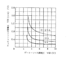
[Problems to be solved by the invention]
Incidentally, the power MOSFET QF generally described above has a drain V-source S voltage VDS vs. a gate TG-source S voltage VGS characteristic as shown in FIG. FIG. 3 shows the characteristics of a TEMPFET that is turned on when a voltage of 4 [V] is applied between the gate TG and the source S and the drain D and the source S are completely conducted. As shown in the figure, when the current ID flowing through the drain D-source S of the TEMPFET is constant, the voltage VDS increases as the voltage VGS decreases, and particularly when the voltage VGS decreases below 4 [V]. To increase. That is, the VDS of the power MOSFET QF increases rapidly when the voltage VGS decreases below a predetermined voltage when the current ID is constant. This is because the resistance between the drain D and source S of the power MOSFET QF increases as the voltage VGS decreases. Therefore, when the drive voltage VP from the booster circuit 61 decreases for some reason, and when a drive voltage VP lower than normal is output to the power MOSFET QF, the voltage VDS increases and the power increases. Heat loss in the MOSFET QF increases.
[0016]
However, since the above-described conventional switching control device and the vehicle power supply device incorporating the switching device monitor the voltage VDS, the voltage VDS does not actually flow between the drain D and the source S of the power MOSFET QF. Cannot be detected. In other words, as a result of the fact that the heat loss of the power MOSFET QF actually increases compared with the normal time, the voltage VDS is cut off for the first time after exceeding the reference voltage Vref4..
[0018]
Therefore, the present invention pays attention to the above-described problems, and a switching control device and a control terminal-load side that can prevent heat generation of the three-terminal switching element due to a decrease in voltage between the control terminal and the load-side terminal. To provide a switching device in which a three-terminal switching element does not generate heat due to a decrease in voltage between terminals, and a vehicle power supply device in which a three-terminal switching element does not generate heat due to a decrease in voltage between a control terminal and a load side terminal Is an issue.
[0019]
[Means for Solving the Problems]
In order to solve the above-mentioned problem, the invention according to
[0020]
According to the first aspect of the present invention, the driving voltage generating means conducts the power supply side terminal-load side terminal by application to the control terminal and turns on the three-terminal switching element. The voltage detection means detects the voltage that determines the voltage between the control terminal and the load side terminal when the three-terminal switching element is turned on, and the drive voltage application control means controls the control terminal according to the load on signal. When the voltage detected by the voltage detection means is equal to or lower than a predetermined value, the application of the drive voltage to the control terminal is stopped even when the load on signal is present.
[0021]
By the way, if the voltage between the control terminal and the load side terminal decreases with a decrease in the drive voltage generated by the drive voltage generating means, the voltage between the power supply side terminal and the load side terminal increases. Loss increases. As a result of heat generation due to this increase in heat loss, the three-terminal switching element may be thermally destroyed, but the voltage that determines the voltage between the control terminal and the load side terminal when the three-terminal switching element is turned on is below a predetermined value. At this time, even when a load on signal is present, by stopping the application of the drive voltage to the control terminal, a voltage equal to or lower than a predetermined value is not applied between the control terminal and the load side terminal.
[0022]
According to a second aspect of the present invention, the voltage detection means controls the difference between the drive voltage generated by the drive voltage generation means and the power supply voltage from the in-vehicle battery when the three-terminal switching element is turned on. The voltage between the terminal and the load side terminal is detected as a voltage to be determined, and the drive voltage application control means is configured such that a difference between the drive voltage detected by the voltage detection means and a power supply voltage from the in-vehicle battery is the predetermined value. 2. The switching control device according to
[0023]
According to the second aspect of the present invention, the difference between the drive voltage generated by the drive voltage generation means by the voltage detection means and the power supply voltage from the in-vehicle battery is calculated as the control terminal-load side terminal when the three-terminal switching element is turned on. When the difference between the drive voltage and the power supply voltage is less than or equal to a predetermined value, the drive voltage application control means stops applying the drive voltage to the control terminal even if a load on signal is present.
[0024]
When the three-terminal switching element is on, the voltage between the power supply side terminal and the load side terminal is extremely small, and the voltage at the load side terminal is equal to the power supply voltage. For this reason, when the three-terminal switching element is turned on, the voltage applied to the control terminal-load side terminal is equal to the difference between the drive voltage and the power supply voltage. Therefore, by setting the difference between the drive voltage and the power supply voltage as the voltage that determines the voltage between the control terminal and the load side terminal when the three-terminal switching element is turned on, even if the drive voltage decreases due to a decrease in the power supply voltage When the three-terminal switching element is turned on, a voltage of a predetermined value or less is not applied between the control terminal and the load side terminal. In addition, by detecting the difference between the drive voltage and the power supply voltage as the voltage between the control terminal and the load side terminal, the plurality of three-terminal switching elements are turned on and off by the drive voltage generated by the single drive voltage generating means. Even if it is a case, it is not necessary to provide a voltage detection means and a drive voltage application control means for every 3 terminal switching element.
[0025]
The invention according to
[0026]
According to the third aspect of the present invention, when the drive voltage application control means applies a drive voltage to the control terminal in response to the load on signal, and the voltage detected by the voltage detection means is less than or equal to the predetermined value, the load on Since the application of the driving voltage to the control terminal is stopped even if a signal is present, a voltage equal to or lower than a value determined by a predetermined value is not applied between the control terminal and the load side terminal.
[0027]
The invention according to
[0028]
According to the fourth aspect of the present invention, when the drive voltage application control means applies the drive voltage to the control terminal in response to the load on signal, and the voltage detected by the voltage detection means is equal to or lower than the predetermined value, the load on Since the application of the driving voltage to the control terminal is stopped even if a signal is present, a voltage equal to or lower than a value determined by a predetermined value is not applied between the control terminal and the load side terminal.
[0029]
The invention according to
[0030]
According to the invention of
[0031]
DETAILED DESCRIPTION OF THE INVENTION
Hereinafter, a switching control device, a switching device, and a vehicle power supply device of the present invention are explained based on a drawing.
FIG. 1 shows an embodiment of a switching control device and a vehicle power supply device incorporating the switching device according to the present invention. In FIG. 1, parts equivalent to those of the conventional device described above with reference to FIG. is doing. In the figure, the power supply voltage VB from the in-
[0032]
In the power MOSFET QF described above, the gate TG is connected to the drive circuit DR, and when the drive voltage VP is supplied from the drive circuit DR when the ignition switch IGSW is in the ON position, the drain D and the source S are electrically connected. Then, the power supply voltage VB is supplied to the
[0033]
In the drive circuit DR, the drive voltage VP obtained by boosting the power supply voltage VB by the booster circuit 21a (for example, VP = VB + 10 [V] when using a TEMPFET that is turned on at VGS = 4 [V] as the MOSFET QF) is connected to the collector. An NPN switching (SW) transistor Tr1 and an NPN switching (SW) transistor Tr2 in which the emitter of the SW transistor Tr1 is connected to the collector. The emitter of the SW transistor Tr1 and the collector of the SW transistor Are connected to the gate TG of the power MOSFET QF. The base of the SW transistor Tr1 is connected to the base of the SW transistor Tr2 via the inverter INV1.
[0034]
Then, the drive circuit DR turns on the SW transistor Tr1 and turns off the SW transistor Tr2, thereby applying the drive voltage VP to the gate TG of the power MOSFET QF to turn on the power MOSFET QF. Also, by turning off the SW transistor Tr1 and turning on the SW transistor Tr2, the application of the drive voltage VP to the gate TG of the power MOSFET QF is stopped and the power MOSFET QF is turned off.
[0035]
Further, the drive voltage VP from the booster circuit 21a (= drive voltage generating means) is supplied to the + input terminal of the differential amplifier 21b to which the power supply voltage VB is supplied to the − input terminal. It functions as detection means and outputs a voltage VPB corresponding to the difference (VP-VB) between the drive voltage VP and the power supply voltage VB. By the way, when the power MOSFET QF is ON, the voltage VDS between the drain D and the source S is extremely small, and the voltage of the source S becomes equal to the power supply voltage VB. Therefore, as the voltage VGS when the power MOSFET QF is turned on, a difference (VP−VB) = voltage VPB between the drive voltage VP output from the differential amplifier 21b and the power supply voltage VB is applied. Therefore, the voltage VPB is a voltage that determines the voltage VG between the gate TG and the source S when the power MOSFET QF is turned on.
[0036]
The voltage VPB output from the differential amplifier 21b is supplied to the positive input terminal of the comparator CP1 to which the reference voltage Vref1 (= predetermined value) obtained by dividing the power supply voltage VB by the resistors R2 and R3 is supplied to the negative input terminal. Supplied. When the voltage VPB drops to a value smaller than the reference voltage Vref1, the comparator CP1 outputs an H level gate-source voltage drop signal S1 to the gate control circuit 21c and to the base of the transistor Tr3. In the transistor Tr3, the collector is connected to the power supply voltage VB via the LED 4 (= alarm generating means) and the emitter is connected to the ground, and the H-level gate-source voltage drop signal S1 is output to the base. And turn on LED4.
[0037]
On the other hand, the shunt resistor Rs provided on the power supply line between the in-
[0038]
The output of the differential amplifier 21 d is analog / digital converted by an A / D converter (not shown) and then supplied to a
[0039]
The above-described
[0040]
Furthermore, as described above, the CPU 22a outputs an H level signal to the base of the SW transistor Tr4 simultaneously with stopping the output of the load on signal S3. The SW transistor Tr4 is turned on when the collector is connected to the power supply voltage VB via the
[0041]
The output of the differential amplifier 21d described above is also supplied to the negative input terminal of the comparator CP2. A reference voltage Vref3 obtained by dividing the power supply voltage VB by the resistors R4 and R5 is supplied to the + input terminal of the comparator CP2. This reference voltage Vref3 is set to a value larger than the above-described reference voltage Vref2. Then, the comparator CP2 outputs an H-level overcurrent detection signal S4 to the gate control circuit 21c while the output of the differential amplifier 21d exceeds the reference voltage Vref3.
[0042]
In the gate control circuit 21c described above, the gate-source voltage drop signal S1 is supplied to one input terminal, the overcurrent detection signal S4 is supplied to the other input terminal, and the OR gate 211c is supplied to one input terminal. The inverted output of the gate 211c includes an AND gate 212c to which the load on signal S3 is supplied to the other input terminal. Therefore, the gate control circuit 21c outputs an H-level on control signal S5 to the base of the transistor Tr1 in response to the input of the load on signal S3, and the gate-source voltage drops even if the load on signal S3 exists. When either one or both of the signal S1 and the overcurrent detection signal S4 are output, the output of the on control signal S5 is stopped and the drive voltage application control means is configured to function.
[0043]
When the on control signal S5 is output from the gate control circuit 21c, the SW transistor Tr1 is turned on and the SW transistor Tr2 is turned off in the drive circuit DR to output the drive voltage VP to the gate TG of the power MOSFET QF. . On the other hand, when the output of the on control signal S5 from the gate control circuit 21c is stopped, the SW transistor Tr1 is turned off and the SW transistor Tr2 is turned on in the drive circuit DR, and the drive voltage VP to the gate TG of the power MOSFET QF is turned on. Output is stopped.
[0044]
The booster circuit 21a, the differential amplifier 21b, the gate control circuit 21c, the differential amplifier 21d, the drive circuit DR, the comparators CP1 and CP2, and the resistors R2 to R4 are formed on one chip. The switching
[0045]
The operation of the switching control device having the above-described configuration and the vehicle power supply device incorporating the switching device will be described below.
First, when the operation switch SW is turned on to output an on operation signal S2 to the
[0046]
For this reason, the output voltage VPB of the differential amplifier 21b corresponding to the difference between the power supply voltage VB and the drive voltage VP (= VP−VB) is also smaller than that in the steady state and is lower than the reference voltage Vref1, so that the comparator CP1 has an H level gate. -The source voltage drop signal S1 is output to the gate control circuit 21c. Due to the output of the gate-source voltage drop signal S1, the gate control circuit 21c does not output the on control signal S5 to the drive circuit DR even when the load on signal S3 is output from the
[0047]
As described above, the difference between the drive voltage VP and the power supply voltage VB (= VP−VB) is detected as the voltage VG between the gate TG and the source S, so that a plurality of drive voltages VP generated by the single booster circuit 21a can be obtained. Even when the power MOSFET QF is turned on / off, it is not necessary to provide the differential amplifier 21b and the gate control circuit 21c for each power MOSFET QF, so that the cost can be reduced.
[0048]
The gate-source voltage drop signal S1 described above is also output to the base of the SW transistor Tr3, and the SW transistor Tr3 is turned on by the output of the gate-source voltage drop signal S1 to supply the power supply voltage VB to the
[0049]
Thereafter, when the turn-on period of the booster circuit 21a ends and the drive voltage VP rises to a steady voltage, the output voltage VPB of the differential amplifier 21b also rises and becomes higher than the reference voltage Vref1. Therefore, the comparator CP1 stops outputting the gate-source voltage drop signal S1. When the output of the gate-source voltage drop signal S1 is stopped, the gate control circuit 21c outputs an H level on control signal S5 to the drive circuit DR in response to the output of the load on signal S3 from the
[0050]
When the power supply line or the like is normal, the current IL flowing through the power MOSFET QF becomes a steady value according to the load resistance of the
[0051]
When the overcurrent detection signal S4 is output even if the load on signal S3 is present, the gate control circuit 21c stops outputting the on control signal S5 and outputs the drive voltage VP to the gate TG from the drive circuit DR. Stop. Since the drain D-source S of the power MOSFET QF changes from the conductive state to the non-conductive state due to the stop of the drive voltage voltage VP, the output voltage of the differential amplifier 21d is reduced as the current IL flowing through the power MOSFET QF decreases. When the voltage becomes lower than the reference voltage Vref3, the comparator CP2 stops outputting the overcurrent detection signal S4. Then, the drive voltage DR is again applied to the gate TG by the drive circuit DR, so that the drain D and the source S of the power MOSFET QF are changed to a conductive state.
[0052]
For this reason, between the drain D and the source S of the power MOSFET QF, the transition from the conductive state to the non-conductive state and the transition from the non-conductive state to the conductive state are repeated, and the current IL flowing through the power MOSFET QF corresponds to the reference voltage Vref3. The current value is suppressed. Since the power MOSFET QF is controlled so that the current IL flowing through the power MOSFET QF does not exceed the current value corresponding to the reference voltage Vref3 when an abnormality occurs in the power line in this way, the power MOSFET QF and the
[0053]
When the cause of this overcurrent is due to a dead short, the state where the current IL is suppressed to the current value corresponding to the reference voltage Vref3 continues. If this state continues, the heat generated in the short-circuit portion accumulates, and the power MOSFET QF and the
[0054]
At this time, the
[0055]
In the above-described embodiment, the difference VPB (= VP-VB) between the drive voltage VP and the power supply voltage VB is used as a voltage that determines the gate voltage TG-source voltage VGS when the power MOSFET QF is turned on. Even if the drive voltage is lowered due to the decrease of the power supply voltage VB, when the power MOSFET QF is turned on, the gate TG-source S is prevented from being applied with a voltage lower than the reference voltage Vref1. The range of voltages that can be applied in the meantime is prevented from changing due to fluctuations in the power supply voltage VB. However, for example, when the drive voltage VP becomes a voltage that determines the voltage VGS when the power MOSFET QF is turned on, when the drive voltage VP is equal to or lower than the reference voltage Vref1 ′ corresponding to the reference voltage Vref1, the drive voltage VP for the gate TG Application may be stopped.
[0056]
In this case, when the power supply voltage VB decreases, the drive voltage VP also decreases. Therefore, even when the reduced voltage is not applied between the gate TG and the source S when the power MOSFET QF is turned on, the drive voltage VP Therefore, it is better to use the in-
[0057]
【The invention's effect】
As described above, according to the first aspect of the present invention, when the voltage that determines the voltage between the control terminal and the load side terminal when the three-terminal switching element is turned on is equal to or lower than the predetermined value, the load on signal is present. However, by stopping the application of the drive voltage to the control terminal, a voltage lower than the value determined by the predetermined value is not applied between the control terminal and the load side terminal, so the voltage between the control terminal and the load side terminal is reduced. Therefore, it is possible to obtain a switching control device that can prevent the three-terminal switching element from generating heat.
[0058]
According to the second aspect of the present invention, the difference between the drive voltage and the power supply voltage is a voltage that determines the voltage between the control terminal and the load side terminal when the three-terminal switching element is turned on. Even if the drive voltage decreases, when the three-terminal switching element is turned on, a voltage lower than a predetermined value is not applied between the control terminal and the load side terminal. The voltage range applied between the control terminal and the load side terminal is not affected by fluctuations in the power supply voltage as compared to the case where the voltage is determined. In addition, by detecting the difference between the drive voltage and the power supply voltage as the voltage between the control terminal and the load side terminal, the plurality of three-terminal switching elements are turned on and off by the drive voltage generated by the single drive voltage generating means. Even if it is, it is not necessary to provide the voltage detection means and the drive voltage application control means for each of the three-terminal switching elements, so that it is possible to obtain a switching control device that achieves cost reduction.
[0059]
According to the invention of
[0060]
According to the fourth aspect of the present invention, when the voltage that determines the voltage between the control terminal and the load side terminal when the terminal switching element is turned on is equal to or lower than the predetermined value, the drive voltage of the control terminal is not affected even if the load on signal exists. By stopping the application, a voltage equal to or lower than a predetermined value is not applied between the control terminal and the load side terminal, so that the three-terminal switching element generates heat due to a decrease in the voltage between the control terminal and the load side terminal. It is possible to obtain a vehicle power supply device that can be prevented in advance.
[0061]
According to the fifth aspect of the present invention, for example, if the function of stopping the application of the drive voltage to the control terminal when an overcurrent flows is provided, the application voltage is identified as the stop of the application of the drive voltage due to the overcurrent. Therefore, it is possible to obtain a vehicular power supply device that allows the user to identify that the stop of application of the drive voltage to the control terminal is due to a decrease in voltage between the control terminal and the load side terminal. .
[Brief description of the drawings]
FIG. 1 is a circuit diagram showing an embodiment of a switching control device and a vehicle power supply device incorporating the switching device of the present invention.
FIG. 2 is a circuit diagram showing an example of a conventional switching control device and a vehicle power supply device incorporating the switching device.
FIG. 3 is a graph showing characteristics of drain-source voltage versus gate-source voltage of a power MOSFET.
[Explanation of symbols]
1 Car battery
3 Load
D Drain (Power supply side terminal)
S source (load side terminal)
TG gate (control terminal)
QF power MOSFET (3-terminal switching element)
21 Switching control device
21a Booster circuit (drive voltage generating means)
21b Differential amplifier (voltage detection means)
S3 Load on signal
Vref1 reference voltage (predetermined value)
21c Gate control circuit (drive voltage application control means)
VB power supply voltage
2 Switching device
4 LED (alarm generating means)
Claims (5)
前記制御端子への印加により前記電源側端子−前記負荷側端子間を導通させて前記3端子スイッチング素子をオンする駆動電圧を、前記車載バッテリからの電源電圧を昇圧して発生する駆動電圧発生手段と、
前記3端子スイッチング素子がオンしたときの前記制御端子−前記負荷側端子間電圧を決定する電圧を検出する電圧検出手段と、
負荷オン信号に応じて前記制御端子に対して前記駆動電圧を印加させ、前記電圧検出手段により検出された前記電圧が所定値以下のとき、前記負荷オン信号が存在しても前記制御端子に対する前記駆動電圧の印加を停止させる駆動電圧印加制御手段と
を備えることを特徴とするスイッチング制御装置。A switching control device that performs on / off control of a three-terminal switching element having a power supply side terminal to which an in-vehicle battery is connected, a load side terminal to which a load is connected, and a control terminal to which a drive voltage is applied,
Drive voltage generating means for generating a drive voltage for turning on the three-terminal switching element by conducting between the power supply side terminal and the load side terminal by application to the control terminal by boosting the power supply voltage from the in-vehicle battery When,
Voltage detection means for detecting a voltage for determining a voltage between the control terminal and the load side terminal when the three-terminal switching element is turned on;
The drive voltage is applied to the control terminal in response to a load on signal, and when the voltage detected by the voltage detection means is equal to or lower than a predetermined value, the load on signal is present even if the load on signal is present. A switching control device comprising: a driving voltage application control unit that stops application of the driving voltage.
前記駆動電圧印加制御手段は、前記電圧検出手段により検出された前記駆動電圧と前記車載バッテリからの電源電圧との差が前記所定値以下のとき、前記負荷オン信号が存在しても前記制御端子に対する前記駆動電圧の印加を停止する
ことを特徴とする請求項1記載のスイッチング制御装置。The voltage detection means calculates a difference between the drive voltage generated by the drive voltage generation means and a power supply voltage from the in-vehicle battery, as a voltage between the control terminal and the load side terminal when the three-terminal switching element is turned on. Detect as the voltage to determine
When the difference between the drive voltage detected by the voltage detection unit and the power supply voltage from the in-vehicle battery is equal to or less than the predetermined value, the drive voltage application control unit is The switching control device according to claim 1, wherein application of the drive voltage to is stopped.
請求項1又は2記載のスイッチング制御装置と
を備えることを特徴とするスイッチング装置。A three-terminal switching element having a power supply side terminal to which an in-vehicle battery is connected, a load side terminal to which a load is connected, and a control terminal to which a drive voltage is applied;
A switching device comprising the switching control device according to claim 1.
該負荷に電源を供給するための車載バッテリと、
車載バッテリが接続される電源側端子、負荷が接続される負荷側端子及び駆動電圧が印加される制御端子を有する3端子スイッチング素子と、
請求項1又は2記載のスイッチング制御装置と
を備えることを特徴とする車両用電源供給装置。The load mounted on the vehicle,
An in-vehicle battery for supplying power to the load;
A three-terminal switching element having a power supply side terminal to which an in-vehicle battery is connected, a load side terminal to which a load is connected, and a control terminal to which a drive voltage is applied;
A vehicle power supply device comprising the switching control device according to claim 1.
を更に備えることを特徴とする請求項4記載の車両用電源供給装置。5. The apparatus according to claim 4, further comprising alarm generation means for generating an alarm for notifying that the application of the drive voltage to the control terminal is stopped when the voltage detected by the voltage detection means is not more than the predetermined value. The power supply apparatus for vehicles as described.
Priority Applications (1)
| Application Number | Priority Date | Filing Date | Title |
|---|---|---|---|
| JP28823299A JP3748343B2 (en) | 1999-10-08 | 1999-10-08 | Switching control device, switching device, and vehicle power supply device |
Applications Claiming Priority (1)
| Application Number | Priority Date | Filing Date | Title |
|---|---|---|---|
| JP28823299A JP3748343B2 (en) | 1999-10-08 | 1999-10-08 | Switching control device, switching device, and vehicle power supply device |
Publications (3)
| Publication Number | Publication Date |
|---|---|
| JP2001109525A JP2001109525A (en) | 2001-04-20 |
| JP2001109525A5 JP2001109525A5 (en) | 2004-07-22 |
| JP3748343B2 true JP3748343B2 (en) | 2006-02-22 |
Family
ID=17727555
Family Applications (1)
| Application Number | Title | Priority Date | Filing Date |
|---|---|---|---|
| JP28823299A Expired - Fee Related JP3748343B2 (en) | 1999-10-08 | 1999-10-08 | Switching control device, switching device, and vehicle power supply device |
Country Status (1)
| Country | Link |
|---|---|
| JP (1) | JP3748343B2 (en) |
Families Citing this family (3)
| Publication number | Priority date | Publication date | Assignee | Title |
|---|---|---|---|---|
| JP5136608B2 (en) * | 2010-07-29 | 2013-02-06 | 株式会社デンソー | Driving device for switching element |
| JP5754414B2 (en) | 2012-05-16 | 2015-07-29 | 株式会社デンソー | Driving device for driven switching element |
| JP6515901B2 (en) * | 2016-10-31 | 2019-05-22 | 京セラドキュメントソリューションズ株式会社 | Image processing device |
-
1999
- 1999-10-08 JP JP28823299A patent/JP3748343B2/en not_active Expired - Fee Related
Also Published As
| Publication number | Publication date |
|---|---|
| JP2001109525A (en) | 2001-04-20 |
Similar Documents
| Publication | Publication Date | Title |
|---|---|---|
| US6617808B2 (en) | Discharge-lamp lighting circuit | |
| US5555725A (en) | Control system for electrically heated catalyst of internal combustion engine | |
| US8422183B2 (en) | Overcurrent detecting apparatus | |
| JPH1041797A (en) | Switch circuit with excess current detecting function | |
| US6936996B2 (en) | Control apparatus for electrical generator of vehicle | |
| JP2000299931A (en) | Power supply control apparatus and method therefor | |
| JP4263685B2 (en) | Protection circuit | |
| JP3748343B2 (en) | Switching control device, switching device, and vehicle power supply device | |
| JP3678953B2 (en) | Overcurrent interruption detection device for semiconductor relay system | |
| JP3567107B2 (en) | Circuit breaker in case of overcurrent | |
| JP2005253154A (en) | Power supply unit | |
| KR19990082549A (en) | A device comprising a thermal protection switching transistor | |
| JP3986041B2 (en) | Power supply control device | |
| JP2006288049A (en) | Load control circuit, current control circuit, and load control system | |
| KR100608215B1 (en) | A driving control apparatus for car cooperation blower motor be possessed of protection function | |
| JP3689280B2 (en) | Method for protecting a semiconductor relay system | |
| JP2000312142A (en) | Intelligent power switch | |
| JPH0649113Y2 (en) | Vehicle power supply | |
| JP2004032966A (en) | Semiconductor switching device | |
| JP2004312955A (en) | Overcurrent detecting circuit and motor drive | |
| CN214984841U (en) | Charging protection system for vehicle | |
| JP7257137B2 (en) | switch device | |
| JP3724780B2 (en) | Power supply control device | |
| JP3465621B2 (en) | Relay drive circuit controller | |
| JP2004236485A (en) | Overcurrent detecting circuit for voltage-driving element |
Legal Events
| Date | Code | Title | Description |
|---|---|---|---|
| A977 | Report on retrieval |
Free format text: JAPANESE INTERMEDIATE CODE: A971007 Effective date: 20051108 |
|
| TRDD | Decision of grant or rejection written | ||
| A01 | Written decision to grant a patent or to grant a registration (utility model) |
Free format text: JAPANESE INTERMEDIATE CODE: A01 Effective date: 20051115 |
|
| RD01 | Notification of change of attorney |
Free format text: JAPANESE INTERMEDIATE CODE: A7426 Effective date: 20051125 |
|
| RD03 | Notification of appointment of power of attorney |
Free format text: JAPANESE INTERMEDIATE CODE: A7423 Effective date: 20051125 |
|
| A61 | First payment of annual fees (during grant procedure) |
Free format text: JAPANESE INTERMEDIATE CODE: A61 Effective date: 20051125 |
|
| R150 | Certificate of patent or registration of utility model |
Free format text: JAPANESE INTERMEDIATE CODE: R150 |
|
| FPAY | Renewal fee payment (event date is renewal date of database) |
Free format text: PAYMENT UNTIL: 20081209 Year of fee payment: 3 |
|
| FPAY | Renewal fee payment (event date is renewal date of database) |
Free format text: PAYMENT UNTIL: 20091209 Year of fee payment: 4 |
|
| FPAY | Renewal fee payment (event date is renewal date of database) |
Free format text: PAYMENT UNTIL: 20101209 Year of fee payment: 5 |
|
| FPAY | Renewal fee payment (event date is renewal date of database) |
Free format text: PAYMENT UNTIL: 20101209 Year of fee payment: 5 |
|
| FPAY | Renewal fee payment (event date is renewal date of database) |
Free format text: PAYMENT UNTIL: 20111209 Year of fee payment: 6 |
|
| LAPS | Cancellation because of no payment of annual fees |