JP3741870B2 - Instruction and data prefetching method, microcontroller, pseudo instruction detection circuit - Google Patents
Instruction and data prefetching method, microcontroller, pseudo instruction detection circuit Download PDFInfo
- Publication number
- JP3741870B2 JP3741870B2 JP22381398A JP22381398A JP3741870B2 JP 3741870 B2 JP3741870 B2 JP 3741870B2 JP 22381398 A JP22381398 A JP 22381398A JP 22381398 A JP22381398 A JP 22381398A JP 3741870 B2 JP3741870 B2 JP 3741870B2
- Authority
- JP
- Japan
- Prior art keywords
- instruction
- data
- pseudo
- address
- transferred
- Prior art date
- Legal status (The legal status is an assumption and is not a legal conclusion. Google has not performed a legal analysis and makes no representation as to the accuracy of the status listed.)
- Expired - Lifetime
Links
- 238000001514 detection method Methods 0.000 title claims description 91
- 238000000034 method Methods 0.000 title claims description 18
- 239000000872 buffer Substances 0.000 claims description 188
- 230000015654 memory Effects 0.000 claims description 99
- 230000004044 response Effects 0.000 description 16
- 230000006870 function Effects 0.000 description 11
- 101100041125 Arabidopsis thaliana RST1 gene Proteins 0.000 description 10
- 101100443250 Saccharomyces cerevisiae (strain ATCC 204508 / S288c) DIG1 gene Proteins 0.000 description 10
- 230000000630 rising effect Effects 0.000 description 8
- 101100443251 Saccharomyces cerevisiae (strain ATCC 204508 / S288c) DIG2 gene Proteins 0.000 description 7
- 101100041128 Schizosaccharomyces pombe (strain 972 / ATCC 24843) rst2 gene Proteins 0.000 description 7
- 230000000717 retained effect Effects 0.000 description 5
- 238000010586 diagram Methods 0.000 description 4
- 238000013481 data capture Methods 0.000 description 1
- 230000007423 decrease Effects 0.000 description 1
- 230000003111 delayed effect Effects 0.000 description 1
- 230000000694 effects Effects 0.000 description 1
- 239000000284 extract Substances 0.000 description 1
- 230000002093 peripheral effect Effects 0.000 description 1
- 239000004065 semiconductor Substances 0.000 description 1
Images


Classifications
-
- G—PHYSICS
- G06—COMPUTING; CALCULATING OR COUNTING
- G06F—ELECTRIC DIGITAL DATA PROCESSING
- G06F9/00—Arrangements for program control, e.g. control units
- G06F9/06—Arrangements for program control, e.g. control units using stored programs, i.e. using an internal store of processing equipment to receive or retain programs
- G06F9/30—Arrangements for executing machine instructions, e.g. instruction decode
- G06F9/38—Concurrent instruction execution, e.g. pipeline or look ahead
- G06F9/3802—Instruction prefetching
- G06F9/3804—Instruction prefetching for branches, e.g. hedging, branch folding
-
- G—PHYSICS
- G06—COMPUTING; CALCULATING OR COUNTING
- G06F—ELECTRIC DIGITAL DATA PROCESSING
- G06F9/00—Arrangements for program control, e.g. control units
- G06F9/06—Arrangements for program control, e.g. control units using stored programs, i.e. using an internal store of processing equipment to receive or retain programs
- G06F9/30—Arrangements for executing machine instructions, e.g. instruction decode
- G06F9/30003—Arrangements for executing specific machine instructions
- G06F9/3005—Arrangements for executing specific machine instructions to perform operations for flow control
- G06F9/30058—Conditional branch instructions
Landscapes
- Engineering & Computer Science (AREA)
- Software Systems (AREA)
- Theoretical Computer Science (AREA)
- Physics & Mathematics (AREA)
- General Engineering & Computer Science (AREA)
- General Physics & Mathematics (AREA)
- Advance Control (AREA)
- Executing Machine-Instructions (AREA)
- Memory System Of A Hierarchy Structure (AREA)
Description
【0001】
【発明の属する技術分野】
本発明は、命令及びデータを先読みする先読み機能を備えたマイクロコントローラに好適な命令及びデータの先読み方法、マイクロコントローラ、疑似命令検出回路に関するものである。
【0002】
【従来の技術】
近年、マイクロコントローラの動作周波数の高速化に伴い、マイクロコントローラの動作速度は日々向上している。マイクロコントローラの動作速度が高速化する一方において、メモリ等の周辺回路の動作速度や、マイクロコントローラのインターフェイスの動作速度がマイクロコントローラの動作速度に追いつかないのが現状である。
【0003】
そこで、マイクロコントローラはキャッシュメモリを備え、マイクロコントローラの高速動作に対応してシステム全体の処理速度を上げるようにしている。しかしながら、キャッシュメモリを備えたマイクロコントローラにおいても、キャッシュのミスヒットが生じた場合には、主メモリからキャッシュメモリにデータを転送しなければならない。その結果、その転送中、命令実行部は待機状態になることから処理速度は低下する。特に、分岐命令等の命令が多く用いられているプログラムではミスヒットする確率が多くなり、処理速度を著しく低下させる。
【0004】
そこで、例えば特開平3−191427号公報において、キャッシュメモリと命令実行部の間にFIFOメモリを設け、即ちキャッシュメモリからFIFOメモリに入力された命令が分岐命令がどうかをFIFOメモリから読み出してチェックする。即ち、命令実行部で処理される前、分岐命令かどうかチェックする。そして、分岐命令である場合には、その分岐先アドレスとキャッシュタグメモリのタグ情報を比較する。そして、比較結果がミスヒットの場合には、その分岐命令の分岐先アドレスにより参照される主メモリのデータ群をキャッシュメモリに転送させる。つまり、命令実行部がその分岐命令を実行する前に検出し、その分岐後の命令を事前にキャッシュメモリに準備させるようにして、キャッシュメモリのミスヒット率を低下させるようにしている。
【0005】
【発明が解決しようとする課題】
しかしながら、特開平3−191427号においては、分岐命令かどうかをチェックするために、読み出すための回路、デコード回路、分岐命令の分岐先アドレスを生成するための特別な回路等が必要であった。これら特別な回路は命令実行部と同程度の複雑な回路構成となり回路規模が大型化する問題があった。
【0006】
又、バッファ(FIFOメモリ)に取り込まれて初めて分岐命令かどうかチェックされるため、命令実行部の実行が速くFIFOメモリに順次取り込まれた命令が命令実行部に速く流れて行く場合には、その分岐後の命令を事前にキャッシュメモリに準備しておくのが遅れるといった問題が生じる。
【0007】
さらに、特開平3−191427号においては、分岐命令を事前に検出し、その分岐先の命令を事前にキャッシュメモリに準備しておくことができるが、データについては事前にキャッシュメモリに準備しておくことができず、データの先読みには対応することができなかった。
【0008】
本発明は、上記問題点を解消するためになされたものであって、その目的は簡単な回路を付加するだけで、命令やデータのミスヒット率を減らしシステム全体の処理速度の向上を図ることができる命令及びデータの先読み方法、マイクロコントローラ、疑似命令検出回路を提供することにある。
【0009】
【課題を解決するための手段】
請求項1に記載の発明は、メモリに記憶されたプログラムの命令及びデータを先読みしその先読みした命令及びデータを先読みバッファに保持する命令及びデータの先読み方法において、前記プログラム中に含まれる命令より前に、その命令の存在を示すとともにその命令のジャンプ先のアドレス又はデータのアドレスを付帯した擬似命令を設定し、その擬似命令を含むプログラムの命令又はデータの先読み時に疑似命令かどうか検出し、擬似命令を検出したとき、その擬似命令に付帯したジャンプ先のアドレス又はデータのアドレスに基づく命令又はデータをメモリから先読みするようした。
請求項2に記載の発明は、請求項1に記載の命令及びデータの先読み方法において、疑似命令は、無条件分岐命令、条件分岐命令、CALL命令、データ呼び出しの命令の少なくともいずれか1の命令に対し、その命令の存在を示す。
【0010】
請求項3に記載の発明は、請求項1又は請求項2に記載の命令及びデータの先読み方法において、前記疑似命令かどうかの検出は、前記メモリに対して前記先読みバッファと並列に接続された疑似命令検出部にて行い、そのメモリからの転送される命令又はデータを先読みバッファと並行して疑似命令検出部に入力させて検出するようにした。
【0011】
請求項4に記載の発明は、請求項1、請求項2又は請求項3に記載の命令及びデータの先読み方法において、前記擬似命令を検出した時、前記疑似命令より後に転送されるその疑似命令に対応する命令が先読み用バッファに転送保持された後に、前記擬似命令に付帯したジャンプ先のアドレス又はデータのアドレスに基づく命令又はデータの先読みしを開始するようにした。
【0012】
請求項5に記載の発明は、請求項1、請求項2、請求項3又は請求項4に記載の命令及びデータの先読み方法において、前記メモリから先読みされる擬似命令に付帯したジャンプ先のアドレス又はデータのアドレスに基づく命令又はデータを、前記先読みバッファとは別に設けた疑似命令用バッファに保持するようにした。
【0013】
請求項6に記載の発明は、請求項1、請求項2、請求項3、請求項4又は請求項5に記載の命令及びデータの先読み方法において、前記擬似命令を検出したとき、擬似命令に付帯したジャンプ先のアドレス又はデータのアドレスに基づく命令又はデータが、少なくとも先読みバッファに保持されていないときに、前記ジャンプ先のアドレス又はデータのアドレスに基づく命令又はデータの先読みしを開始するようにした。
【0014】
請求項7に記載の発明は、メモリに記憶されたプログラムの命令及びデータを先読みバッファに転送し、命令実行部がアドレスカウンタに基づいて前記先読みバッファから前記命令及びデータを読み出し解読し実行するマイクロコントローラにおいて、先読みバッファに転送される前記プログラムの命令及びデータから、命令より前に該命令の存在を示すとともに該命令のジャンプ先のアドレス又はデータのアドレスを付帯した疑似命令を検出する疑似命令検出部と、前記疑似命令検出部が疑似命令を検出したとき、該疑似命令の付帯したジャンプ先のアドレス又はデータのアドレスに基づく命令又はデータをメモリから先読みさせるアドレス制御部とを設けた。
請求項8に記載の発明は、請求項7に記載のマイクロコントローラにおいて、疑似命令は、無条件分岐命令、条件分岐命令、CALL命令、データ呼び出しの命令の少なくともいずれか1の命令に対し、その命令の存在を示す。
【0015】
請求項9に記載の発明は、請求項7又は請求項8に記載のマイクロコントローラにおいて、前記アドレス制御部に基づいて先読みされるジャンプ先のアドレス又はデータのアドレスに基づく命令又はデータを保持する疑似命令用バッファを備えた。
【0016】
請求項10に記載の発明は、請求項7、請求項8又は請求項9に記載のマイクロコントローラにおいて、前記アドレス制御部は、前記擬似命令検出部が擬似命令を検出したとき、該擬似命令に付帯するジャンプ先のアドレス又はデータのアドレスに基づいて少なくとも先読みバッファにジャンプ先のアドレス又はデータのアドレスに基づく命令又はデータが保持されているかどうかチェックし、保持されていないとき、同ジャンプ先のアドレス又はデータのアドレスに基づく命令又はデータをメモリから先読みさせる。
【0017】
請求項11に記載の発明は、請求項7、請求項8、請求項9又は請求項10に記載のマイクロコントローラにおいて、前記疑似命令検出部は、前記メモリに対して前記先読みバッファと並列に接続されるように、メモリに対して先読みバッファとの間に接続されたデータ線からメモリから転送される命令又はデータを入力し、前記疑似命令及び同疑似命令に付帯するジャンプ先のアドレス又はデータのアドレスを検出する。
【0018】
請求項12に記載の発明は、転送されるオペコード及びオペランドをデータ線から入力し、特定の命令を事前に知らせるために予め設定された擬似命令のオペコードを検出する擬似命令検出回路において、前記オペコードから求めたその命令長又はオペコードに続くオペランドの数とオペコード及びオペランドの転送周期とでオペコードの転送時期を検出し、オペランドが転送されている時、オペコードの検出動作を無効にし、オペコードが転送されている時、オペコードの検出動作を有効にする検出タイミング回路を設けた。
【0020】
(作用)
請求項1に記載の発明によれば、疑似命令は対応する命令より先に先読みバッファに転送されるため、疑似命令と対応する命令は転送される前に事前にわかる。そして、擬似命令に付帯したジャンプ先のアドレス又はデータのアドレスに基づく命令又はデータをメモリから先読みすることから、疑似命令は対応する命令が命令実行部で実行される時、ミスヒットすることなく直ちにその分岐先アドレスの命令又はデータを命令実行部に取り込むことができる。
請求項2に記載の発明によれば、疑似命令では、無条件分岐命令、条件分岐命令、CALL命令、データ呼び出しの命令の少なくともいずれか1の命令に対し、その命令の存在が示される。
【0021】
請求項3に記載の発明によれば、先読みされるメモリからの命令又はデータは、先読みバッファに転送されると同時に疑似命令検出部に転送され疑似命令かどうかが検出される。従って、疑似命令の検出は、先読みバッファに保持された後でなく、メモリから転送された時に検出がなされるため、より早い時期に疑似命令の検出ができる。その結果、擬似命令に付帯したジャンプ先のアドレス又はデータのアドレスに基づく命令又はデータをメモリから先読みする時期をより早くすることができる。又、疑似命令検出部は、先読みバッファに保持された命令又はデータを用いて疑似命令を検出するのではなく、メモリから先読みのために転送されてくる命令又はデータを直接入力し検出している。従って、疑似命令検出部は、先読みバッファとの間で命令又はデータを読み出すための特別な回路を必要としない簡単な回路で構成することができる。
【0022】
請求項4に記載の発明によれば、疑似命令に対応する命令が先読み用バッファに保持された後に、前記擬似命令に付帯したジャンプ先のアドレス又はデータのアドレスに基づく命令又はデータの先読みを開始するため、ジャンプ先のアドレス又はデータのアドレスに基づく命令又はデータを優先して転送している途中において、先読みバッファに基づく命令が全て命令実行部で実行処理されてしまって待機状態となることはない。
【0023】
請求項5に記載の発明によれば、先読みバッファとは別に設けた疑似命令用バッファを設け、その疑似命令用バッファに擬似命令に付帯したジャンプ先のアドレス又はデータのアドレスに基づく命令又はデータを保持させるようにした。従って、擬似命令に付帯したジャンプ先のアドレス又はデータのアドレスに基づく命令又はデータを先読みして疑似命令用バッファに保持している間、命令実行部は先読みバッファから命令又はデータを読み出し解読及び処理を実行することができる。
【0024】
請求項6に記載の発明によれば、擬似命令を検出した時、該擬似命令に付帯するジャンプ先のアドレス又はデータのアドレスに基づいて少なくとも先読みバッファにジャンプ先のアドレス又はデータのアドレスに基づく命令又はデータが保持されてない場合に、メモリから先読み行う。従って、無駄な先読みがなくなり効率の良い先読み処理を行なうことができる。
【0025】
請求項7に記載の発明によれば、疑似命令は対応する命令より先に先読みバッファに転送されるとともに、疑似命令検出部にて該疑似命令は対応する命令が転送される前に事前にわかる。そして、アドレス制御部にて擬似命令に付帯したジャンプ先のアドレス又はデータのアドレスに基づく命令又はデータはメモリから先読みされる。従って、疑似命令は対応する命令が命令実行部で実行される時、ミスヒットすることなく直ちにその分岐先アドレスの命令又はデータは命令実行部に取り込むことができる。
請求項8に記載の発明によれば、疑似命令では、無条件分岐命令、条件分岐命令、CALL命令、データ呼び出しの命令の少なくともいずれか1の命令に対し、その命令の存在が示される。
【0026】
請求項9に記載の発明によれば、先読みバッファとは別に設けた疑似命令用バッファを設け、その疑似命令用バッファに擬似命令に付帯したジャンプ先のアドレス又はデータのアドレスに基づく命令又はデータが保持される。従って、擬似命令に付帯したジャンプ先のアドレス又はデータのアドレスに基づく命令又はデータを先読みして疑似命令用バッファに保持している間、命令実行部は先読みバッファから命令又はデータを読み出し解読及び処理を実行することができる。
【0027】
請求項10に記載の発明によれば、アドレス制御部は擬似命令検出部が擬似命令を検出したとき、該擬似命令に付帯するジャンプ先のアドレス又はデータのアドレスに基づいて少なくとも先読みバッファにジャンプ先のアドレス又はデータのアドレスに基づく命令又はデータが保持されてない場合のみに、メモリから先読みさせる。従って、無駄な先読みがなくなり効率の良い先読み処理を行なうことができる。
【0028】
請求項11に記載の発明によれば、メモリからの命令又はデータは、先読みバッファに転送されると同時に疑似命令検出部に転送され疑似命令かどうかが検出される。従って、疑似命令の検出は、先読みバッファに保持された後でなく、メモリから転送された時に検出がなされるため、より早い時期に疑似命令の検出ができる。その結果、擬似命令に付帯したジャンプ先のアドレス又はデータのアドレスに基づく命令又はデータをメモリから先読みする時期をより早くすることができる。又、疑似命令検出部は、先読みバッファに保持された命令又はデータを用いて疑似命令を検出するのではなく、メモリから先読みのために転送されてくる命令又はデータを直接入力し検出している。従って、疑似命令検出部は、先読みバッファとの間で命令又はデータを読み出すための特別な回路を必要としない簡単な回路となる。
【0029】
請求項12に記載の発明によれば、擬似命令検出回路は、検出タイミング回路により、データ線にオペコードが転送されている時、その転送されているオペコードの検出する。従って、検出タイミング回路により、オペランドに擬似命令のオペコードと同じ値が存在した場合でもそのオペランドを擬似命令のオペコードと誤検出することはない。
【0031】
【発明の実施の形態】
(第1実施形態)
以下、本発明を具体化した一実施形態を図1〜図4に従って説明する。図1はは、マイクロコントローラの要部ブロック回路を示す。
【0032】
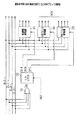
図1において、マイクロコントローラ10は、先読み回路部11と命令実行部12を備えている。マイクロコントローラ10は1チップの半導体集積回路装置で形成されている。
【0033】
先読み回路部11は、メモリとしてのメインメモリ13からプログラムの命令及びデータを順次入力し保持する。命令実行部12は、アドレスカウンタ14が示すアドレスADを先読み回路部11に出力し、そのアドレスADの命令又はデータを先読み回路部11に要求する。先読み回路部11はその要求に応じて命令又はデータを命令実行部12に出力する。そして、命令実行部12は取り込んだ命令又はデータを解読し必要な処理動作を実行する。
【0034】
又、先読み回路部11は、メインメモリ13から転送されてくるプログラムの命令及びデータのうち予め用意されている疑似命令が転送されてきたかどうかチェックするようになっている。
【0035】
ここで疑似命令とは、組み立てられたプログラム中に存在する分岐命令の前に存在し、その分岐命令の存在を事前に示すための命令である。従って、疑似命令が転送されて来たとき、疑似命令の後にその疑似命令に対応する分岐命令が転送されてくることがわかる。又、この疑似命令は、前記命令実行部12ではノーオペレーション(NOP)命令と同じに取り扱われるように定義されている。
【0036】
尚、本実施形態では、分岐命令は、無条件分岐命令、条件分岐命令、CALL命令、及び、データ呼び出しの命令を含む。又、本実施形態では、疑似命令のオペコードは、アセンブラで「1、1、1、1」が割り当てられている。
【0037】
疑似命令は、命令長が4であって、「命令(オペコード)」、「付加情報(オペランド)」、「上位アドレス(オペランド)」及び「下位アドレス(オペランド)」の順に構成されている。上位アドレスは疑似命令に対応する分岐命令が示す分岐先アドレスADX中の上位アドレスを示し、下位アドレスは疑似命令に対応する分岐命令が示す分岐先アドレスADX中の下位アドレスを示す。
【0038】
先読み回路部11は、疑似命令が転送されると、その疑似命令に付帯する分岐命令が示す分岐先アドレスADXに対応するプログラムの命令を前記メインメモリ13から取り込むようになっている。従って、疑似命令の後に転送された分岐命令が命令実行部12で実行される時には、その分岐先アドレスADXの命令は既に先読み回路部11に用意されていることから、ミスヒットすることなく直ちにその分岐先アドレスADXの命令は命令実行部12に取り込まれることになる。
【0039】
図1において、先読み回路部11は、疑似命令検出部21、FIFO(ファーストインファーストアウト)メモリよりなる先読みバッファ22、先読みバッファ用タグメモリ(以下、第1タグという)23、FIFO(ファーストインファーストアウト)メモリよりなる疑似命令用バッファ24、疑似命令用バッファ用タグメモリ(以下、第2タグという)25、アドレス制御部26、第1及び第2ゲート回路27,28、及び、バイパスゲート回路29を備えている。
【0040】
疑似命令検出部21は、メインメモリ13と先読みバッファ22との間に設けられ、メインメモリ13から先読みバッファ22に順次転送されるプログラムの命令及びデータが疑似命令かどうかチェックする。詳述すると、図2に示すように、疑似命令検出部21は、メインメモリ13と先読みバッファ22との間を結ぶ4ビットのデータ線DL0〜DL3に接続され、メインメモリ13から先読みバッファ22に順次転送される命令及びデータを直接入力する。
【0041】
疑似命令検出部11は、疑似命令検出回路31、シフトレジスタ32、付加情報保持回路33、上位アドレス保持回路34、下位アドレス保持回路35とから構成されている。
【0042】
疑似命令検出回路31は4入力端子を備えたアンド回路にて構成されていて、その4入力端子は対応するデータ線DL0〜DL3に接続されている。疑似命令検出回路31は、データ線DL0〜DL3に転送されている命令又はデータが全てHレベル(高電位)、即ち「1,1,1,1」の時、該転送されている命令が疑似命令であるとしてHレベルなる検出信号SXを次段のシフトレジスタ32に出力する。尚、転送されている命令が疑似命令でないとき、データ線DL0〜DL3のうちすくなくとも1つのデータがLレベル(低電位)になる。従って、疑似命令検出回路31はLレベルなる検出信号SXをシフトレジスタ32に出力する。
【0043】
シフトレジスタ32は、検出信号SXの他にリードストローブ信号RSTを入力する。リードストローブ信号RSTは、マイクロコントローラ10内で生成されるクロック信号であって、このリードストローブ信号RSTの周期で、メインメモリ13からの命令及びデータが読み込まれるようになっている。
【0044】
シフトレジスタ32は3出力端子を備え、各出力端子から対応する保持回路33〜35に対して保持信号SFA,SFB,SFCを出力するようになっている。つまり、図4に示すように、シフトレジスタ32は、Hレベルの検出信号SXを入力しリードストローブ信号RSTのLレベルからHレベルの立ち上がりで保持する。その保持した状態で、シフトレジスタ32は次の新たなリードストローブ信号RSTがLレベルからHレベルの立ち上がると、保持信号SFAのみをHレベルにする。そして、保持信号SFAがHレベルの状態で次のリードストローブ信号RSTがLレベルからHレベルの立ち上がると、シフトレジスタ32は保持信号SFAをLレベルにし保持信号SFBのみをHレベルにする。さらに、保持信号SFBがHレベルの状態で次のリードストローブ信号RSTがLレベルからHレベルの立ち上がると、シフトレジスタ32は保持信号SFBをLレベルにし保持信号SFCのみをHレベルにする。そして、保持信号SFCのみがHレベルの状態で、次のリードストローブ信号RSTがLレベルからHレベルの立ち上がると、シフトレジスタ32は全ての保持信号SFA,SFB,SFCをLレベルにする。
【0045】
付加情報保持回路33は、4個のD型フリップフロップにて構成されている。各D型フリップフロップのデータ入力端子は対応するデータ線DL0〜DL3に接続されている。各D型フリップフロップの制御入力端子には保持信号SFAが入力される。そして、各D型フリップフロップは、保持信号SFAのHレベルの立ち上がりに応答して、その時のデータ線DL0〜DL3に転送されている内容を保持する。
【0046】
つまり、付加情報保持回路33は、4ビットの疑似命令の転送後であって、次のリードストローブ信号RSTに基づいて転送される該疑似命令のための4ビットよりなる「付加情報」を保持信号SFAに応答して保持するようになっている。
【0047】
上位アドレス保持回路34は、4個のD型フリップフロップにて構成されている。各D型フリップフロップのデータ入力端子は対応するデータ線DL0〜DL3に接続されている。各D型フリップフロップの制御入力端子には保持信号SFBが入力される。そして、各D型フリップフロップは、保持信号SFBのHレベルの立ち上がりに応答して、その時のデータ線DL0〜DL3に転送されている内容を保持する。
【0048】
つまり、上位アドレス保持回路34は、前記4ビットの「付加情報」の転送後であって、次のリードストローブ信号RSTに基づいて転送される8ビットよりなる分岐先アドレスADX中の上位4ビットのアドレス、即ち「上位アドレス」を保持信号SFBに応答して保持するようになっている。
【0049】
下位アドレス保持回路35は、4個のD型フリップフロップにて構成されている。各D型フリップフロップのデータ入力端子は対応するデータ線DL0〜DL3に接続されている。各D型フリップフロップの制御入力端子には保持信号SFCが入力される。そして、各D型フリップフロップは、保持信号SFCのHレベルの立ち上がりに応答して、その時のデータ線DL0〜DL3に転送されている内容を保持する。
【0050】
つまり、下位アドレス保持回路35は、前記4ビットの「上位アドレス」の転送後であって、次のリードストローブ信号RSTに基づいて転送される前記8ビットよりなる分岐先アドレスADX中の下位4ビットのアドレス、即ち「下位アドレス」を保持信号SFCに応答して保持するようになっている。
【0051】
従って、上位アドレス保持回路34が保持している「上位アドレス」と、下位アドレス保持回路35が保持している「下位アドレス」をあわせることによって、リードストローブ信号RSTの二周期で転送される疑似命令に付帯させた分岐先のアドレスADXが求まることになる。
【0052】
先読みバッファ22は、前記メインメモリ13とデータ線DL0〜DL3を介して接続されている。先読みバッファ22は、アドレス制御部26からの第1の取り込み信号RST1に基づいてメインメモリ13から順次転送されるプログラムの命令及びデータを取り込むようになっている。先読みバッファ22は、第1ゲート回路27を介して前記命令実行部12に接続されている。そして、先読みバッファ22に取り込まれた命令及びデータは、アドレス制御部26からの第1のゲート信号SG1にて第1ゲート回路27が開くことにより命令実行部12に転送されるようになっている。
【0053】
第1タグ23は、先読みバッファ22に取り込まれた命令及びデータにおける先頭アドレスと最終アドレスを記憶している。
疑似命令用バッファ24は、前記メインメモリ13とデータ線DL0〜DL3を介して接続されている。疑似命令用バッファ24は、アドレス制御部26からの第2の取り込み信号RST2に基づいてメインメモリ13から順次転送されるプログラムの命令及びデータを取り込むようになっている。本実施形態では、前記疑似命令検出部11が疑似命令を検出し、メインメモリ13から転送されるその疑似命令に付帯した分岐先アドレスADXに対応するプログラムの命令及びデータが、疑似命令用バッファ24に取り込まれるようになっている。
【0054】
疑似命令用バッファ24は、第2ゲート回路28を介して前記命令実行部12に接続されている。そして、疑似命令用バッファ24に取り込まれた命令及びデータは、アドレス制御部26からの第2のゲート信号SG2にて第2ゲート回路28が開くことにより命令実行部12に転送されるようになっている。
【0055】
第2タグ25は、疑似命令用バッファ24に取り込まれた命令及びデータにおける先頭アドレスと最終アドレスを記憶している。
又、メインメモリ13はバイパスゲート回路29を介して前記命令実行部12に接続されている。そして、メインメモリ13から転送される命令及びデータは、アドレス制御部26からのバイパス信号BPSにてバイパスゲート回路29が開くことにより命令実行部12に転送されるようになっている。
【0056】
つまり、本実施形態では、メインメモリ13から各バッファ23,24への命令及びデータの取り込み及び各バッファ23,24から命令実行部12への命令及びデータの転送は、アドレス制御部26が行っている。
【0057】
図3は、アドレス制御部26を説明するための回路構成を示す。
図3において、先読み用アドレス比較回路41は、前記命令実行部12のアドレスカウンタ14が示すアドレスADと前記第1タグ23が保持しているアドレスとを入力して両アドレスを比較する。そして、アドレスカウンタ14が示すアドレスADと第1タグ23のアドレスが一致する場合、先読み用アドレス比較回路41はLレベルの第1のゲート信号SG1を第1ゲート回路27に出力する。従って、Lレベルの第1のゲート信号SG1に応答して第1ゲート回路27は開く。その結果、アドレスカウンタ14のアドレスADと一致するアドレスの命令又はデータは、先読みバッファ22から読み出され、第1ゲート回路27を介して命令実行部12に転送される。
【0058】
反対に、アドレスカウンタ14が示すアドレスADと先頭アドレスが一致しない場合、先読み用アドレス比較回路41はHレベルの第1のゲート信号SG1を第1ゲート回路27に出力する。従って、Hレベルの第1のゲート信号SG1に応答して第1ゲート回路27は閉じる。その結果、先読みバッファ22の先頭アドレスにある命令又はデータは、第1ゲート回路27を介して命令実行部12に転送されない。
【0059】
疑似命令用アドレス比較回路42は、前記命令実行部12のアドレスカウンタ14が示すアドレスADと前記第2タグ25が保持しているアドレスとを入力して両アドレスを比較する。そして、アドレスカウンタ14が示すアドレスADと第2タグ26のアドレスが一致する場合、疑似命令用アドレス比較回路42は、Lレベルの第2のゲート信号SG2を第2ゲート回路28に出力する。従って、Lレベルの第2のゲート信号SG2に応答して第2ゲート回路28は開く。その結果、アドレスカウンタ14のアドレスADと一致するアドレスの命令又はデータは、疑似命令用バッファ24から読み出されて、第2ゲート回路28を介して命令実行部12に転送される。
【0060】
反対に、アドレスカウンタ14が示すアドレスADと第2タグ25のアドレスが一致しない場合、疑似命令用アドレス比較回路42はHレベルの第2のゲート信号SG2を第2ゲート回路28に出力する。従って、Hレベルの第2のゲート信号SG2に応答して第2ゲート回路28は閉じる。その結果、疑似命令用バッファ24の命令又はデータは、第2ゲート回路28を介して命令実行部12に転送されない。
【0061】
ナンド回路43は、第1及び第2のゲート信号SG1,SG2を入力する。そして、第1及び第2のゲート信号SG1,SG2が共にHレベルの時(先読み用及び疑似命令用アドレス比較回路41,42が共にアドレスADと先頭アドレスが一致しないと判断した時)に、ナンド回路43はLレベルの出力信号を出力する。Lレベルの出力信号は、待機信号WTとして命令実行部12に出力する。
【0062】
そして、命令実行部12は、Lレベルの待機信号WTに応答として命令実行部12は必要な処理動作を停止する。つまり、待機信号WTがLレベルの時には新たな命令又はデータが先読みバッファ22及び疑似命令用バッファ24から取り込まれないため、命令実行部12は必要な処理動作を実行することができず、新たな命令又はデータの取り込みを待つ。
【0063】
又、このナンド回路43の出力信号(待機信号WT)は、第3のゲート信号SG3として第1アドレスゲート回路44に出力される。第1アドレスゲート回路44は、アドレスカウンタ14が示すアドレスADを入力する。第1アドレスゲート回路44は、Lレベルの第3のゲート信号SG3を入力したとき、アドレスカウンタ14のアドレスADを次段の第2アドレスゲート回路45に出力する。第2アドレスゲート回路45は、第1アドレスゲート回路44を介してアドレスカウンタ14のアドレスADを入力すると、該アドレスADをメインメモリ13に出力する。従って、メインメモリ13は、該アドレスADの命令及びデータを読み出し先読み回路部11に出力することになる。
【0064】
又、このナンド回路43の出力信号(待機信号WT)は、バイパス信号BPSとしてバイパスゲート回路29に出力される。そして、Lレベルのバイパス信号BPSに応答してバイパスゲート回路29が開くことにより、メインメモリ13から取り込まれる命令及びデータは同バイパスゲート回路29を介して命令実行部12に直接転送される。反対に、Hレベルのバイパス信号BPSがHレベルのときバイパスゲート回路29は閉じる。バイパスゲート回路29は閉じることにより、メインメモリ13から取り込まれる命令及びデータは同バイパスゲート回路29を介して命令実行部12に転送されることはない。
【0065】
つまり、命令実行部12は、先読みバッファ22及び疑似命令用バッファ24にアドレスカウンタ14が示すアドレスADの命令又はデータがない場合のときにメインメモリ13から転送される命令及びデータをバイパスゲート回路29を介して直接取り込むことができるようになっている。
【0066】
先読み用アドレス保持回路46は、前記第1タグ23が保持しているその時の最終アドレスを入力しメインメモリ13から次に先読みバッファ22に取り込むアドレス(最終アドレスの次のアドレス)を生成し保持する。又、先読み用アドレス保持回路46は先読みバッファ22に対してメインメモリ13からの命令及びデータがこれ以上取り込めないフル状態においては、これ以上の取り込みはできない旨のフルアドレスを生成し保持するようになっている。
【0067】
先読み用アドレスゲート回路47は、先読み用アドレス保持回路46が保持するアドレスを入力するとともに、前記待機信号WTを入力する。
先読み用アドレスゲート回路47は、Hレベルの待機信号WTを入力している時、第1タグ23が保持しているアドレス(最終アドレスの次のアドレス)を第2アドレスゲート回路45に出力する。この時、先読み用アドレスゲート回路47は、第1取り込み信号RST1を生成し、該信号RST1を先読みバッファ22に出力する。
第2アドレスゲート回路45は、先読み用アドレスゲート回路47を介して先読み用アドレス保持回路46が保持するアドレスを入力すると、該アドレスをメインメモリ13に出力する。従って、メインメモリ13は、該アドレスの命令及びデータを読み出し先読み回路部11に出力することになる。そして、先読み回路部11の先読みバッファ22は、前記第1取り込み信号RST1に応答してメインメモリ13からの命令及びデータを取り込むようになっている。
【0068】
疑似命令用アドレス保持回路48は、前記第2タグ25が保持しているその時の最終アドレスを入力しメインメモリ13から次に疑似命令用バッファ24に取り込むアドレス(最終アドレスの次のアドレス)を生成し保持する。又、疑似命令用アドレス保持回路48は疑似命令用バッファ24に対してメインメモリ13からの命令及びデータがこれ以上取り込めないフル状態においては、これ以上の取り込みはできない旨のフルアドレスを生成し保持するようになっている。
【0069】
疑似命令用アドレスゲート回路49は、疑似命令用アドレス保持回路48が保持するアドレスを入力するとともに、前記待機信号WTを入力する。又、疑似命令用アドレスゲート回路49は、疑似命令検出部31からの分岐先アドレスADXを入力する。
【0070】
疑似命令用アドレスゲート回路49は、Hレベルの待機信号WTを入力している時、分岐先アドレスADX又は疑似命令バッファ用タグメモリ25が保持しているアドレス(最終アドレスの次のアドレス)を第2アドレスゲート回路45に出力する。この時、疑似命令用アドレスゲート回路49は、第2取り込み信号RST2を生成し、該信号RST2を疑似命令用バッファ24に出力する。
【0071】
第2アドレスゲート回路45は、疑似命令検出部31からの分岐先アドレスADX又は疑似命令用アドレス保持回路48が保持するアドレスを入力すると、該アドレスをメインメモリ13に出力する。従って、メインメモリ13は、該アドレスの命令及びデータを読み出し先読み回路部11に出力することになる。そして、先読み回路部11の疑似命令用バッファ24は、前記第2取り込み信号RST2に応答してメインメモリ13からの命令及びデータを取り込むようになっている。
【0072】
又、本実施形態では、第2アドレスゲート回路45は、第1アドレスゲート回路44、先読みアドレスゲート回路47及び疑似命令用アドレスゲート回路49からそれぞれアドレスを入力するが、第1アドレスゲート回路44のアドレスを優先的に選択し、その次に第2アドレスゲート回路45のアドレスを選択するようになっている。又、本実施形態では、説明の便宜上、疑似命令用アドレスゲート回路49のアドレスが選択されたとき、第1アドレスゲート回路44からのアドレスの入力を除き先読みアドレスゲート回路47からのアドレスの入力があっても、疑似命令用アドレスゲート回路49のアドレスがフルアドレスになるまで選択し続けるようにしている。そして、選択されたアドレスはメインメモリ13に出力されるようになっている。
【0073】
次に上記のように構成したマイクロコントローラ10の作用について説明する。
今、疑似命令用バッファ24は何も記憶されていない状態で、メインメモリ13から先読みバッファ22にプログラムの命令及びデータがデータ線DL0〜DL3を介して順次転送されている場合について説明する。又、先読みバッファ22に転送されたプログラムの命令及びデータが命令実行部12に順次転送され実行処理されている。従って、アドレス制御回路部26の先読み用アドレス比較回路41は第1のゲート信号SG1を出力するとともに、ナンド回路43を介して出力される待機信号WTはHレベルとなっている。
【0074】
又、アドレス制御回路部26の先読み用アドレスゲート回路47は、第1取り込み信号RST1を出力している。さらに、疑似命令用バッファ24は何も記憶されていない状態で、アドレス制御回路部26の疑似命令用アドレスゲート回路49は第2取り込み信号RST2を出力していない。
【0075】
従って、第2アドレスゲート回路45は、先読みアドレスゲート回路47を介して先読み用アドレス保持回路46からのアドレスを選択して該アドレスをメインメモリ13に転送している。
【0076】
このような状態において、疑似命令検出部21の疑似命令検出回路31はそのデータ線DL0〜DL3を先読みバッファ22に転送されていくプログラムの命令及びデータを入力する。そして、疑似命令検出回路31が、「1,1,1,1」なる疑似命令のオペコードを検出すると、疑似命令検出部21の上位アドレス保持回路34及び下位アドレス保持回路35において、前記疑似命令に付帯させた分岐先のアドレスADXが保持される。上位アドレス保持回路34及び下位アドレス保持回路35に保持された前記疑似命令に付帯させた分岐先のアドレスADXは、アドレス制御回路部26の疑似命令用アドレスゲート回路49に出力される。
【0077】
疑似命令用アドレスゲート回路49は、この時点では待機信号WTはHレベルであり、疑似命令用アドレス保持回路48は疑似命令用バッファ24は何も記憶されていないことから、このアドレスADXを第2アドレスゲート回路45に出力する。第2アドレスゲート回路45は、このアドレスADXを入力すると、先読み用アドレス回路47からのアドレスがフルアドレスかどうかチェックし、フルアドレスになるまで該アドレスADXを選択しない。そして、先読み用アドレス回路47からのアドレスがフルアドレスになると、第2アドレスゲート回路45は、該アドレスADXを選択しメインメモリ13に出力する。該アドレスADXを選択されると、疑似命令用アドレスゲート回路49は、第2の取り込み信号RST2を出力する。又、第2アドレスゲート回路45は、フルアドレスになると、第1の取り込み信号RST1を消失させる。
【0078】
メインメモリ13はこのアドレスADXの命令及びデータを読み出し出力する。この時、疑似命令用アドレスゲート回路49は、第2取り込み信号RST2を出力しているため、このアドレスADXの命令及びデータは、疑似命令用バッファ24に転送される。
【0079】
アドレスADXの命令及びデータが疑似命令用バッファ24に転送されると、第2タグ25を介して疑似命令用アドレス保持回路48から疑似命令用アドレスゲート回路49にアドレスADXに1加算したアドレスが出力される。疑似命令用アドレスゲート回路49はこのアドレスADXに1加算したアドレスを第2アドレスゲート回路45を介してメインメモリ13に出力する。アドレスADXに1加算したアドレスの命令及びデータが読み出され疑似命令用バッファ24に転送される。
【0080】
以後、同様な動作が繰り返されて、疑似命令用バッファ24に分岐先のアドレスADXを先頭に命令及びデータが記憶される。
やがて、疑似命令用バッファ24がこれ以上命令及びデータを取り込めないフル状態になると、疑似命令用アドレス保持回路48からフルアドレスを示すデータが疑似命令用アドレスゲート回路49に出力される。
【0081】
疑似命令用アドレスゲート回路49はこのフルアドレスを示すデータに基づいて第2の取り込み信号RST2の生成を停止し該信号RST2の疑似命令用バッファ24への出力を停止する。又、疑似命令用アドレスゲート回路49はこのフルアドレスを示すデータを第2アドレスデータゲート回路45に出力する。
【0082】
第2アドレスデータゲート回路45は、フルアドレスを示すデータに基づいて前記先読み用アドレスゲート回路47のアドレスを選択する状態になる。前記先読み用アドレスゲート回路47は、第1タグ23に基づくアドレスを第2アドレスデータゲート回路45に出力するとともに、第1の取り込み信号RST1を先読みバッファ22に出力する。
【0083】
メインメモリ13はこの先読み用アドレス保持回路46からのアドレスの命令及びデータを読み出し出力する。この時、先読み用アドレスゲート回路47は、第1取り込み信号RST1を出力しているため、このアドレスの命令及びデータは、先読みバッファ22に転送される。即ち、先読みバッファ22への命令及びデータの転送が再開される。
【0084】
アドレスの命令及びデータが先読みバッファ22に転送されると、先読み用アドレス保持回路46から先読み用アドレスゲート回路47に先のアドレスに1加算したアドレスが出力される。先読み用アドレスゲート回路47はこの1加算されたアドレスを第2アドレスゲート回路45を介してメインメモリ13に出力する。1加算されたアドレスの命令及びデータが読み出され先読みバッファ22に転送される。
【0085】
以後、同様な動作が繰り返されて、先読みバッファ22に命令及びデータが記憶される。やがて、先読みバッファ22がこれ以上命令及びデータを取り込めないフル状態に再びなると、先読み用アドレス保持回路46からフルアドレスを示すデータが先読み用アドレスゲート回路47に出力される。
【0086】
先読み用アドレスゲート回路47はこのフルアドレスを示すデータに基づいて第1の取り込み信号RST1の生成を停止し該信号RST1の先読みバッファ22への出力を停止する。又、先読み用アドレスゲート回路47はこのフルアドレスを示すデータを第2アドレスデータゲート回路45に出力する。
【0087】
第2アドレスデータゲート回路45は、フルアドレスを示すデータに基づいて前記先読み用アドレスゲート回路47のアドレスを非選択にする状態になり、メインメモリ13にアドレスを出力するのを停止する。
【0088】
次に、上記のように構成したマイクロコントローラの特徴について述べる。
(1)本実施形態では、組み立てられたプログラムにおいて、そのプログラム中に存在する分岐命令の前にその分岐命令の存在を事前に示すための疑似命令を設けた。そして、組み立てられたプログラムの命令及びデータを先読みバッファ22に転送する途中において、疑似命令検出部21にて転送されている命令が疑似命令かどうか検出するようにした。従って、分岐命令が先読みバッファ22に転送される前に事前に分岐命令が転送されて来ることがわかる。その結果、疑似命令の後に転送された分岐命令が命令実行部12で実行される時、その分岐先アドレスADXの命令を既に疑似命令用バッファ24に用意させておくことができため、ミスヒットすることなく直ちにその分岐先アドレスADXの命令は命令実行部12に取り込むことがてきる。
【0089】
(2)本実施形態では、疑似命令検出部21は、メインメモリ13と先読みバッファ22との間に接続されたデータ線DL0〜DL3と接続し、メインメモリ13から先読みバッファ22に転送する途中の命令及びデータを入力して疑似命令を検出する。従って、先読みバッファ22に転送される前に疑似命令の検出することができる。その結果、疑似命令の後に転送された分岐命令が命令実行部12で実行される時、その分岐先アドレスADXの命令を既に疑似命令用バッファ24に用意させておくことができため、ミスヒットすることなく直ちにその分岐先アドレスADXの命令は命令実行部12に取り込むことがてきる。
【0090】
(3)本実施形態の疑似命令検出部21は、アンド回路よりなる疑似命令検出回路31、シフトレジスタ32、及び、D型フリップフロップよりなる各保持回路33〜34等の非常に簡単な回路で構成したので、マイクロコントローラがより複雑になることが防止できる。
【0091】
(4)本実施形態では、疑似命令検出部21は、先読みバッファ22に転送される前に疑似命令の有無を検出するようにした。つまり、疑似命令の検出のために、先読みバッファ22との間でデータの授受を行うことがなことから、先読みバッファ22との間に特別かつ複雑な検出のための回路を設ける必要ない。その結果、マイクロコントローラの回路構成が複雑になることが防止できる。
【0092】
(5)本実施形態では、分岐命令が示す分岐先ドレスADXを疑似命令に付帯させた。そして、疑似命令検出部21は疑似命令の転送を検出したとき、あわせて分岐命令が示す分岐先ドレスADXを抽出してアドレス制御部26に出力する。アドレス制御部26は分岐先ドレスADXに基づいてメインメモリ13から命令及びデータを読み出し疑似命令用バッファ24に転送させるようにした。従って、分岐先アドレスADXに対応するプログラムの命令は前記メインメモリ13から取り込むことができ、疑似命令の後に転送された分岐命令が命令実行部12で実行される時には、その分岐先アドレスADXの命令は既に疑似命令用バッファ24に用意されていることから、ミスヒットすることなく直ちにその分岐先アドレスADXの命令は命令実行部12に取り込むことがてきる。
【0093】
(6)本実施形態では、待機信号WTがHレベルの時、即ち、命令実行部12がメインメモリ13から命令及びデータを直接読み出していない期間に、先読みバッファ22及び疑似命令用バッファ24に命令及びデータを転送するようにしたので、効率よくメインメモリ13を使用することができ、メインメモリ13から単位時間当たりの読み出し命令数の向上を図ることができる。
【0094】
(7)本実施形態によれば、先読みバッファ22とは別に疑似命令用バッファ24を設け、その疑似命令用バッファ24に擬似命令に付帯したジャンプ先のアドレスADXに基づく命令及データを転送させるようにした。従って、擬似命令に付帯したジャンプ先のアドレスADXに基づく命令及データを先読みし疑似命令用バッファ24に保持している間、命令実行部12は、停止することはなく、アドレスカウンタ14に基づいて先読みバッファ22から命令及びデータを読み出し解読及び処理を実行することができる。
【0095】
(第2実施形態)
次に、本発明の第2実施形態について説明する。本実施形態は、疑似命令検出部21が第1実施形態と相違する。従って、説明の便宜上、疑似命令検出部21についてのみ説明する。
【0096】
前記実施形態では、疑似命令のオペコードをアセンブラで「1、1、1、1」とし、そのオペコードをアンド回路よりなる疑似命令検出回路31で検出するようにしたものである。そして、上記実施形態の場合、オペコードに続くオペランドに「1、1、1、1」よりなるオペランドがないものとしている。つまり、「1、1、1、1」よりなるオペランドが存在した場合に、このオペランドによって疑似命令として誤検出してしまうからである。
【0097】
そこで、本実施形態では、オペランドに「1、1、1、1」よりなるオペランドが存在しても、誤検出しない疑似命令検出回路21を説明する。
尚、本実施形態では、全てのオペコードは、4ビットよりなり、その上位2ビット(最上位ビットをD3、最上位ビットD3の次の下位ビットをD2とする)は、オペコードに続くオペランドの数を示すように定義されている。
【0098】
本実施形態では、「D3、D2」が「0、0」の時、オペランドの数は無し。「D3、D2」が「0、1」の時、オペランドの数は1つ。「D3、D2」が「1、0」の時、オペランドの数は2つ。「D3、D2」が「1、1」の時、オペランドの数は3つ。
【0099】
従って、疑似命令のオペコードは「1、1、1、1」であって、その上位2ビットは、「1、1」なので、疑似命令のオペランドの数は3つ、即ち、付加情報、上位アドレス及び下位アドレスの3つのオペランドとなる。又、ある命令のオペコードが「1、0、1、1」のとき、その上位2ビットは、「1、0」なので、その命令のオペランドの数は2つとなる。
【0100】
図5は、本実施形態の疑似命令検出回路21を示す。尚、第1実施形態と同じ回路構成については、符号を同じにしその詳細は省略し相違する構成について説明する。
【0101】
本実施形態の疑似命令検出回路31は、5入力よりなるアンド回路より構成され、それぞれデータ線DL0〜DL3に接続されている。又、残る1つの入力端子は、検出タイミング回路としてのダウンカウンタ50に接続されている。本実施形態の疑似命令検出回路31は、データ線DL0〜DL3に転送される命令及びデータが全て「1」であって、ダウンカウンタ50から出力される出力信号が「1」のとき、Hレベルの検出信号SXを出力することになる。
【0102】
ダウンカウンタ50は、セット入力端子が、上位2ビットD3、D2が転送されデータ線DL3,DL2に接続されている。そして、ダウンカウンタ50は、「D3,D2」が「0,0」の時に「0」、「D3,D2」が「0,1」の時に「1」、「D3,D2」が「1,0」の時に「2」、「D3,D2」が「1,1」の時に「3」の値を、出力信号が「0」から「1」になるとき保持し、次の新たなリードストローブ信号RSTの立ち上がりでセットされるようになっている。
【0103】
ダウンカウンタ50は、そのセットされた値を前記リードストローブ信号RSTの立ち上がりで「1」づつ減算する。そして、ダウンカウンタ50は、減算値が「0」になった時、「1」の出力信号を疑似命令検出回路31に出力する。従って、ダウンカウンタ50は、減算値が「0」以外の時、「0」の出力信号を疑似命令検出回路31に出力する。その結果、疑似命令検出回路31は、出力信号が「0」の時には疑似命令の検出ができない。
【0104】
ダウンカウンタ50の出力信号は、同カウンタ50の制御入力端子に入力される。ダウンカウンタ50は、制御信号入力端子に出力信号が「0」から「1」になったとき、データ線DL3,DL2から上位2ビットD3,D2の値を保持し、保持した後に出力信号を「1」から「0」にする。ダウンカウンタ50は、制御信号入力端子に出力信号が「0」のときには、データ線DL3,DL2から上位2ビットD3,D2の値をセットしない。
【0105】
次に上記のよう構成した疑似命令検出部21の作用を説明する。
今、「1,0,…,…」よりなるオペコードよりなるある命令の後、疑似命令が転送されるものとする。従って、ある命令のオペコードの上位ビットD3,D2は「1,0」てあるため、オペランドの数は2となる。
【0106】
そして、ある命令の「1,0,…,…」のオペコードが転送されている状態であって、ダウンカウンタ50の出力信号が「0」から「1」になった状態で、疑似命令検出回路31は、オペコードが「1,0,…,…」で「0」を含むので、疑似命令でない判断する。一方、ダウンカウンタ50は、出力信号の「0」から「1」に応答してこのオペコードの上位ビットD3,D2の「1,0」即ち「2」を保持するとともに、出力信号を「1」から「0」にする。
【0107】
そして、ダウンカウンタ50は、次にリードストローブ信号RSTの立ち上がりで「2」をセットする。このリードストローブ信号RSTの立ち上がり時に、「1,0,…,…」のオペコードよりなるある命令の1つ目のオペランドが転送されるが、疑似命令検出回路31は、出力信号が「0」なのでこのオペランドを入力しても疑似命令の検出をしない。
【0108】
続いて、新たなリードストローブ信号RSTが立ち上がりがでダウンカウンタ50は、減算値が「1」となる。このリードストローブ信号RSTの立ち上がり時に、2つ目のオペランドが転送されるが、疑似命令検出回路31は、出力信号が「0」なのでこのオペランドを入力しても疑似命令の検出はしない。
【0109】
2つ目のオペランドが転送されて次の疑似命令のオペコードが転送されると、次の新たなリードストローブ信号RSTが立ち上がり、その立ち上がりでダウンカウンタ50は、減算値が「0」となり出力信号を「1」にする。従って、疑似命令検出回路31は、「1」の出力信号に基づいて検出可能となる。この時、疑似命令における「1,1,1,1」のオペコードが転送されているので、Hレベルの検出信号SXを出力する。
【0110】
一方、ダウンカウンタ50は、上位ビットD3,D2の「1,1」即ち「3」を保持し保持した後、出力信号を「1」から「0」にする。以後同様な動作を繰り返し、3つのオペランドが転送されても、その間、疑似命令検出回路31は、疑似命令の検出は行わない。つまり、疑似命令検出回路31の検出時期を常にオペーコードが転送されている間に限定している。
【0111】
従って、本実施形態では、オペランドに疑似命令と同じ内容のものが存在しても、そのオペランドを疑似命令と誤検出することはない。その結果、プログラムを設計する際の自由度は向上する。
【0112】
尚、この第2実施形態では、オペコードからオペランドの数をダウンカウンタ50にセットしたが、オペランドの数に1加算してなる命令長をダウンカウンタ50にセットして実施してもよい。この場合には、ダウンカウンタ50はリードストローブ信号RSTの立ち上がりで保持及び減算を行なうことになる。
【0113】
尚、発明の実施の形態は、上記各実施形態に限定されるものではなく以下のように実施してもよい。
○前記実施形態では、疑似命令検出部21が疑似命令を検出した時先読みバッファ22がフルアドレスになった後に、疑似命令検出部21が検出した分岐命令におけるジャンプ先のアドレスADXに基づいてメインメモリ13から命令及びデータを疑似命令用バッファ24に転送するようにした。
【0114】
これを、疑似命令検出部21が疑似命令を検出した時、先読みバッファ22への命令及びデータ転送が、その疑似命令に対応する分岐命令が先読みバッファ22に転送されまで、中止させないようして実施してもよい。
【0115】
この場合、疑似命令に付帯する付加情報に疑似命令が転送されてから対応する分岐命令がどれくらい後に転送されるかの情報を記録する。そして、この付加情報を、例えば図3に破線で示すように、先読みアドレス保持回路46に出力する。先読みアドレス保持回路46は、この付加情報に基づいて、疑似命令が転送されてから対応する分岐命令の転送が完了したとき、第2アドレスゲート回路45に対して疑似命令用アドレスゲート49を優先的に選択させる信号を出力させる機能を持たせる。
【0116】
このように、構成することによって、先読みバッファ22に対する先読みが長くなりすぎて疑似命令に対応する分岐命令が命令実行部12にて処理される前に、ジャンプ先のアドレスADXに基づいてメインメモリ13から命令及びデータを疑似命令用バッファ24に転送されていないといった問題はなくなる。
【0117】
○前記実施形態では、先読みバッファ22がフルアドレスになった後に、疑似命令検出部21が検出した分岐命令におけるジャンプ先のアドレスADXに基づいてメインメモリ13から命令及びデータを疑似命令用バッファ24に転送するようにした。
【0118】
これを、先読みバッファ22への命令及びデータ転送を一旦中止し、疑似命令検出部21が検出した分岐命令におけるジャンプ先のアドレスADXに基づいてメインメモリ13から命令及びデータを疑似命令用バッファ24に転送するようにして実施してもよい。
【0119】
この場合、疑似命令検出部21が疑似命令を検出した時、先読みバッファ22への命令及びデータ転送が、その疑似命令に対応する分岐命令が先読みバッファ22に転送されまで、中止させないようして変更して実施してもよい。
【0120】
この場合も、疑似命令に付帯する付加情報に疑似命令が転送されてから対応する分岐命令がどれくらい後に転送されるかの情報を記録する。そして、この付加情報を、例えば図3に破線で示すように、先読みアドレス保持回路46に出力する。先読みアドレス保持回路46は、この付加情報に基づいて、疑似命令に対する分岐命令が先読みバッファ22に転送されるまでの間、第2アドレスゲート回路45に対して優先的に選択させる機能を持たせる。
【0121】
このように、構成することによって、疑似命令用バッファ24にジャンプ先のアドレスADXに基づいてメインメモリ13から命令及びデータを転送している途中において、先読みバッファ22に基づく命令が全て命令実行部12で実行処理されてしまって待機状態となることが防止できる。
【0122】
又、この先読みバッファ22に分岐命令が転送された後に、疑似命令用バッファ24へのジャンプ先のアドレスADXに基づいて命令及びデータの転送する場合について、命令及びデータが疑似命令用バッファ24にこれ以上取り込めないフル状態になった時、先読みバッファ22にまだ取り込む余裕があっる時、アドレス制御部26は、先読みバッファ22に書き込むようにしてもよい。
【0123】
○前記実施形態では、無条件分岐、条件分岐、CALL命令、データ呼び出しの命令を分岐命令とし、その分岐命令に対して疑似命令を作成したが、分岐命令に対して疑似命令を設定したが、無条件分岐、条件分岐、CALL命令、データ呼び出しの命令の少なくともいずれか1つの命令に対して疑似分岐命令を設定してもよい。
【0124】
○前記実施形態では、疑似命令は命令実行部12ではノーオペレーション(NOP)命令と同じに取り扱われる。そして、疑似命令の命令長は4であるので、命令実行部12は疑似命令を処理するためにその命令長4のサイクルだけ無駄な処理をすることになる。
【0125】
そこで、疑似命令検出部21が疑似命令を検出した時、アドレス制御部26にその疑似命令の1つ前の命令又はデータのアドレスを保持させ、命令実行部12のアドレスカウンタ14がそのアドレスになり、そして次のアドレスにカウントアップするとき、疑似命令のアドレスを飛ばし疑似命令の次に来る命令又はデータのアドレスまでアップさせる機能を持たせるようにして実施してもよい。
【0126】
この場合、命令実行部12は、疑似命令の処理を実行することなく直ちに疑似命令の次に来る命令又はデータを処理することになり、処理時間の短縮を図ることができる。
【0127】
○本実施形態では、疑似命令検出部21にて疑似命令が検出されると、その疑似命令に付帯する分岐命令が示す分岐先アドレスADXに対応する命令及びデータをメインメモリ13から読み出すようにしている。これを疑似命令検出部21にて検出した分岐先アドレスADXに基づく命令及びデータが先読みバッファ22又は疑似命令用バッファ24に既に保持されているかチェックする機能をバス制御部26に持たせ、既に保持されている場合には先読みをしないようにし、保持されていない時には疑似命令用バッファ24に命令及びデータを先読みさせるようにする。この場合、バス制御部26による既に保持されているかチェックは、例えば分岐先アドレスADXと第1タグ23及び第2タグ25のタグ情報を比較して行う。
【0128】
このようにすることにより、無駄な先読みがなくなり、効率の良い先読み処理を行うことができる。
○前記実施形態では、無条件分岐命令、条件分岐命令、CALL命令、データ呼び出しの命令を1つの擬似命令として取り扱い、オペコードを「1,1,1,1」としたが、これを無条件分岐命令、条件分岐分岐、CALL命令、及び、データ呼び出しの命令に対してそれぞれ相違するオペコードの擬似命令を設定してもよい。
【0129】
そして、無条件分岐命令の擬似命令に付帯する付加情報に、該無条件命令が先読みバッファ22に転送されるまで先読みし、その後はジャンプ先の命令及びデータを擬似命令用バッファ24に転送させるような情報を付加する。そして、その付加情報に基づいてアドレス制御部26に上記動作を実行させるようにしてもよい。
【0130】
又、条件分岐命令の擬似命令に付帯する付加情報に、該条件分岐命令が先読みバッファ22に転送されるまで先読みし、その後はジャンプ先の命令及びデータを擬似命令用バッファ24に転送させる動作と、先読みバッファ22に転送する通常の転送動作を行なわせるような情報を付加する。そして、その付加情報に基づいてアドレス制御部26に上記動作を実行させるようにしてもよい。このとき、交互にかえるタイミングは、その転送する命令及びデータ数の割合で決定して行なってもよい。
【0131】
さらに、CALL命令の擬似命令に付帯する付加情報に、該CALL命令が先読みバッファ22に転送されるまで先読みし、続いてジャンプ先の命令及びデータを最後まで擬似命令用バッファ24に転送させ、その後に再び先読みバッファ22を使用した先読みを行なわせるような情報を付加する。そして、その付加情報に基づいてアドレス制御部26に上記動作を実行させるようにしてもよい。
【0132】
さらに又、データ呼び出し命令の擬似命令に付帯する付加情報に、該データ呼び出し命令が先読みバッファ22に転送されるまで先読みし、続いて擬似命令用バッファ24に必要な分のデータを転送し、その後は引き続き先読みバッファ22への先読みを行なわせるような情報を付加する。そして、その付加情報に基づいてアドレス制御部26に上記動作を実行させるようにしてもよい。
【0133】
○前記実施形態では、無条件分岐命令、条件分岐命令、CALL命令、データ呼び出しの命令を1つの擬似命令として取り扱い、オペコードを「1,1,1,1」としたが、これをオペコードは共通とし、無条件分岐命令、条件分岐分岐、CALL命令、及び、データ呼び出しの命令の区別を付加情報に定義して実施してもよい。
【0134】
○前記実施形態では、1つの疑似命令用バッファ24だけであった。これを無条件分岐命令、条件分岐命令、CALL命令、データ呼び出しの命令の各命令の対する疑似命令をそれぞれを区別できるようにするとともに、無条件分岐命令、条件分岐命令、CALL命令、データ呼び出しの命令の各命令のための専用の疑似命令用バッファをそれぞれ設ける。そして、アドレス制御部26に無条件分岐命令の疑似命令の場合には無条件分岐命令のために設けたバッファにジャンプ先のアドレスの命令及びデータを転送させる等、各命令に対応するバッファにその命令及びデータを転送させる機能をもたせて実施してもよい。
【0135】
○又、無条件分岐命令、条件分岐命令、及び、CALL命令に対する疑似命令のオペーコードを「1,1,1,1」とし、データ呼び出しの命令に対する擬似命令のオペコードを「1,1,1,0」にする。つまり、擬似命令のオペコードの最下位ビットを「0」にして他の疑似命令と相違させて実施してもよい。この場合、疑似命令検出回路31は、上位3ビットのオペコードをデータ線DL1〜DL3から入力する。そして、オペコードの最下位ビットが転送されるデータ線DL0からその最下位ビットをアドレス制御部26に出力する。
【0136】
そして、アドレス制御部26に疑似検出回路部21からの疑似命令の検出に基づいてその時の最下位ビットの内容(「1」か「0」)で、データ呼び出しの命令に対する擬似命令なのか、それ以外の疑似命令なのか判断する機能を持たせる。さらに、データ呼び出しの命令に対する擬似命令の場合には、該データ呼び出し命令が先読みバッファ22に転送されるまで先読みし、続いて擬似命令用バッファ24に必要な分のデータを転送し、その後は引き続き先読みバッファ22への先読みを行なわせる機能をアドレス制御部26に持たせるようにして実施してもよい。
【0137】
○又、疑似命令に付帯する付加情報に優先順位の情報を付加する。そして、その付加情報に基づいて先読みバッファ22の先読みを優先的に行ったり、疑似命令用バッファ24の先読みを優先的に実行させる等の機能をバス制御部26に持たせて実施してもよい。
【0138】
○前記実施形態では、先読みバッファ22及び疑似命令用バッファ24をFIFOメモリで構成したが、それぞれキャッシュメモリで構成してもよい。
○前記実施形態では、先読みバッファ22と疑似命令用バッファ24をそれぞれ設けたが、これを1つの記憶容量が大きいFIFOメモリよりなるバッファを共用するようにし、疑似命令が検出されたとき、疑似命令に対する命令がバッファに転送されるまで先読みし、続いてジャンプ先の命令及びデータを最後まで先読みを行なわせる等の機能をバス制御部26に持たせて実施してもよい。
【0139】
【発明の効果】
請求項1,2に記載の発明によれば、ミスヒットすることなく直ちにその分岐先アドレスの命令及びデータを命令実行部に取り込むことができる。
【0140】
請求項3に記載の発明によれば、ミスヒットすることなく直ちにその分岐先アドレスの命令及びデータを命令実行部に取り込むことがてきるとともに、簡単な回路で実施することができる。
【0141】
請求項4に記載の発明によれば、先読みバッファに基づく命令が全て命令実行部で実行処理されてしまって待機状態となることはなくマイクロコントローラの効率のよい処理動作を可能にすることができる。
【0142】
請求項5に記載の発明によれば、擬似命令に付帯したジャンプ先のアドレス又はデータのアドレスに基づく命令及データを先読みし疑似命令用バッファに保持している間、命令実行部は先読みバッファから命令及びデータを読み出し解読及び処理を実行することができ、マイクロコントローラの効率のよい処理動作を可能にすることができる。
【0143】
請求項6に記載の発明によれば、無駄な先読みをなくすことができ効率の良い先読み処理を行なうことができる。
請求項7,8に記載の発明によれば、ミスヒットすることなく直ちにその分岐先アドレスの命令及びデータは命令実行部に取り込むことができる。
【0144】
請求項9に記載の発明によれば、擬似命令に付帯したジャンプ先のアドレス又はデータのアドレスに基づく命令及データを先読みし疑似命令用バッファに保持している間、命令実行部は先読みバッファから命令及びデータを読み出し解読及び処理を実行することができ、マイクロコントローラの効率のよい処理動作を可能にすることができる。
【0145】
請求項10に記載の発明によれば、無駄な先読みをなくすことができ効率の良い先読み処理を行なうことができる。
請求項11に記載の発明によれば、ミスヒットすることなく直ちにその分岐先アドレスの命令及びデータを命令実行部に取り込むことがてきるとともに、簡単な回路で実施することができる。
【0146】
請求項12に記載の発明によれば、擬似命令を確実に検出することができる。
【図面の簡単な説明】
【図1】一実施形態を説明するための先読み回路部を備えたマイクロコントローラの要部ブロック回路図
【図2】疑似命令検出部の構成を説明するためのブロック回路図
【図3】アドレス制御部の構成を説明するためのブロック回路図
【図4】疑似命令検出部の動作を説明するためのタイミングチャート
【図5】疑似命令検出部の別例を説明するためのブロック回路図
【符号の説明】
10 マイクロコントローラ
11 先読み回路部
12 命令実行部
13 メインメモリ
14 アドレスカウンタ
21 疑似命令検出部
22 先読みバッファ
23 先読みバッファ用タグメモリ
24 疑似命令用バッファ
25 疑似命令バッファ用タグメモリ
26 アドレス制御部
31 疑似命令検出回路
50 ダウンカウンタ
ADX 分岐先アドレス
DL0〜DL3 データ線[0001]
BACKGROUND OF THE INVENTION
The present invention relates to an instruction and data prefetching method suitable for a microcontroller having a prefetching function for prefetching instructions and data, a microcontroller, and a pseudo instruction detection circuit.On the roadIt is related.
[0002]
[Prior art]
In recent years, the operation speed of the microcontroller has been improved day by day as the operation frequency of the microcontroller has been increased. While the operation speed of the microcontroller is increased, the operation speed of peripheral circuits such as a memory and the operation speed of the interface of the microcontroller cannot keep up with the operation speed of the microcontroller.
[0003]
Therefore, the microcontroller includes a cache memory so as to increase the processing speed of the entire system corresponding to the high-speed operation of the microcontroller. However, even in a microcontroller having a cache memory, if a cache miss occurs, data must be transferred from the main memory to the cache memory. As a result, the processing speed decreases because the instruction execution unit is in a standby state during the transfer. In particular, in a program in which many instructions such as branch instructions are used, the probability of a miss hit increases, and the processing speed is significantly reduced.
[0004]
Therefore, for example, in Japanese Patent Laid-Open No. 3-191427, a FIFO memory is provided between the cache memory and the instruction execution unit, that is, the instruction input from the cache memory to the FIFO memory is read from the FIFO memory and checked. . That is, it is checked whether it is a branch instruction before being processed by the instruction execution unit. If it is a branch instruction, the branch destination address is compared with the tag information of the cache tag memory. When the comparison result is a miss hit, the data group of the main memory referred to by the branch destination address of the branch instruction is transferred to the cache memory. That is, the instruction execution unit detects the branch instruction before executing the branch instruction, and prepares the instruction after the branch in the cache memory in advance, thereby reducing the miss hit rate of the cache memory.
[0005]
[Problems to be solved by the invention]
However, in Japanese Patent Application Laid-Open No. 3-191427, a circuit for reading, a decoding circuit, a special circuit for generating a branch destination address of a branch instruction, and the like are necessary to check whether the instruction is a branch instruction. These special circuits have a complicated circuit configuration similar to that of the instruction execution unit, and there is a problem that the circuit scale is increased.
[0006]
In addition, since it is checked whether or not it is a branch instruction for the first time after being fetched into the buffer (FIFO memory), if the instructions sequentially fetched into the FIFO memory flow quickly to the instruction execution unit, There is a problem that it is delayed to prepare the instruction after branching in the cache memory in advance.
[0007]
Furthermore, in JP-A-3-191427, a branch instruction can be detected in advance and the branch destination instruction can be prepared in advance in the cache memory. However, data is prepared in advance in the cache memory. It was not possible to keep track of the data.
[0008]
The present invention has been made to solve the above-mentioned problems, and its object is to reduce the miss hit rate of instructions and data by simply adding a simple circuit and to improve the processing speed of the entire system. Instruction and data prefetching method, microcontroller, pseudo instruction detection timesThe roadIt is to provide.
[0009]
[Means for Solving the Problems]
The invention according to claim 1, MeAn instruction and data prefetching method for prefetching program instructions and data stored in memory and holding the prefetched instructions and data in a prefetch buffer, included in the programLifeBefore the instruction, set the pseudo-instruction indicating the presence of the instruction and the jump destination address or data address of the instruction and including the pseudo-instructionOrAn instruction based on the jump destination address or data address attached to the pseudo instruction when a pseudo instruction is detected when data prefetching is detected.OrdataTheLook ahead from Mori.
According to a second aspect of the present invention, in the instruction and data prefetching method according to the first aspect, the pseudo instruction is an instruction of at least one of an unconditional branch instruction, a conditional branch instruction, a CALL instruction, and a data call instruction. Indicates the existence of the instruction.
[0010]
Claim3The invention described in claim 1Or claim 2In the instruction and data prefetching method according to claim 1, whether or not the pseudo instruction is detected isMemoIs executed by a pseudo-instruction detection unit connected in parallel to the prefetch buffer.NoInstructions transferred from memoryOrData is input to the pseudo-instruction detection unit in parallel with the prefetch buffer and detected.
[0011]
Claim4The invention described in claim 1, Claim 2 or claim 3In the instruction and data prefetching method according to claim 1, when the pseudoinstruction is detected, an instruction corresponding to the pseudoinstruction transferred after the pseudoinstruction is transferred and held in the prefetching buffer, and then attached to the pseudoinstruction. Instruction based on the jump destination address or data addressOrThe prefetching of data was started.
[0012]
Claim5The invention described in claim 1, Claim 2, claim 3OrClaim 4In the prefetching method of instructions and data described inMemoInstruction based on jump destination address or data address attached to pseudo-instruction prefetched from memoryOrThe data is held in a pseudo instruction buffer provided separately from the prefetch buffer.
[0013]
Claim6The invention described in claim1, claim 2, claim 3, claim 4OrClaim 5An instruction based on the jump destination address or data address attached to the pseudo instruction when the pseudo instruction is detectedOrAn instruction based on the jump destination address or data address when data is not held at least in the prefetch bufferOrThe prefetching of data was started.
[0014]
Claim7The invention described in, MeThe instruction and data of the program stored in the memory are transferred to the prefetch buffer, and the instruction execution unit reads the instruction and data from the prefetch buffer based on the address counter, and decodes and executes the instruction and data. From instructions and data of the program,lifeA pseudo-instruction detection unit that detects the pseudo-instruction that indicates the presence of the instruction before the instruction and includes the jump destination address or data address of the instruction, and the pseudo-instruction detection unit detects the pseudo-instruction, Instructions based on jump destination addresses or data addresses attached to pseudo instructionsOrdataTheAnd an address control unit for prefetching from the memory.
According to an eighth aspect of the present invention, in the microcontroller according to the seventh aspect, the pseudo instruction corresponds to at least one of an unconditional branch instruction, a conditional branch instruction, a CALL instruction, and a data call instruction. Indicates the presence of an instruction.
[0015]
Claim9The invention described in claim7 or claim 8An instruction based on a jump destination address or data address prefetched based on the address control unitOrA pseudo-instruction buffer for holding data is provided.
[0016]
Claim10The invention described in claim7. Claim 8OrClaim 9In the microcontroller according to claim 1, when the pseudo-instruction detection unit detects a pseudo-instruction, the address control unit jumps to a prefetch buffer at least based on a jump-destination address or data address attached to the pseudo-instruction. Instruction based on address or address of dataOrCheck whether data is retained, and if not, instructions based on the jump destination address or data addressOrdataTheRead ahead from Mori.
[0017]
Claim11The invention described in claim7, claim 8, claim 9OrClaim 10In the microcontroller according to claim 2, the pseudo instruction detection unitMemoTo be connected in parallel with the prefetch buffer, MeWhether the data line connected to the read-ahead buffer for memoryLameInstructions transferred from memoryOrData is input, and the jump instruction address or data address attached to the pseudo instruction and the pseudo instruction is detected.
[0018]
Claim12The pseudo-instruction detection circuit for detecting the operation code of the pseudo-instruction set in advance to input the operation code and operand to be transferred from the data line and informing a specific instruction in advance is obtained from the operation code. When the opcode transfer time is detected by the number of operands following the instruction length or opcode, the opcode and the operand transfer cycle, and when the operand is transferred, the opcode detection operation is disabled and the opcode is transferred A detection timing circuit for enabling the operation of detecting the opcode is provided.
[0020]
(Function)
According to the first aspect of the present invention, since the pseudo instruction is transferred to the prefetch buffer prior to the corresponding instruction, the instruction corresponding to the pseudo instruction is known in advance before the transfer. And an instruction based on the jump destination address or data address attached to the pseudo instructionOrdataTheSince prefetching from memory, the pseudo-instruction is an instruction at the branch destination address immediately without a miss hit when the corresponding instruction is executed in the instruction execution unit.OrData can be taken into the instruction execution unit.
According to the second aspect of the present invention, in the pseudo instruction, the presence of the instruction is indicated for at least one of the unconditional branch instruction, the conditional branch instruction, the CALL instruction, and the data call instruction.
[0021]
Claim3According to the invention described inRumeInstruction from MoriOrThe data is transferred to the prefetch buffer and simultaneously transferred to the pseudo instruction detection unit to detect whether it is a pseudo instruction. Therefore, the detection of pseudo-instructions is not after being held in the look-ahead buffer., MeSince the detection is performed when the data is transferred from the memory, the pseudo instruction can be detected earlier. As a result, instructions based on jump destination addresses or data addresses attached to pseudo instructionsOrdataTheThe time to look ahead from Mori can be made earlier. In addition, the pseudo-instruction detection unit uses instructions stored in the prefetch buffer.OrRather than using data to detect pseudo-instructions, MeInstructions transferred from Mori for read aheadOrData is directly input and detected. Therefore, the pseudo-instruction detection unit sends instructions to the prefetch buffer.OrA simple circuit that does not require a special circuit for reading data can be used.
[0022]
Claim4According to the invention, the instruction based on the jump destination address or data address attached to the pseudo instruction after the instruction corresponding to the pseudo instruction is held in the prefetch buffer.OrInstruction based on jump destination address or data address to start prefetching dataOrWhile data is preferentially transferred, all instructions based on the prefetch buffer are not executed in the instruction execution unit and are not in a standby state.
[0023]
Claim5According to the invention, the pseudo instruction buffer provided separately from the prefetch buffer is provided, and the instruction based on the jump destination address or data address attached to the pseudo instruction in the pseudo instruction buffer is provided.OrData was retained. Therefore, an instruction based on the jump destination address or data address attached to the pseudo instructionOrWhile the data is prefetched and stored in the pseudo-instruction buffer, the instruction execution unit executes instructions from the prefetch buffer.OrData can be read and decrypted and processed.
[0024]
Claim6According to the invention described in (1), when a pseudo instruction is detected, an instruction based on a jump destination address or data address in at least a prefetch buffer based on a jump destination address or data address attached to the pseudo instructionOrIf no data is retained, MeRead ahead from Mori. Therefore, useless prefetching is eliminated and efficient prefetching processing can be performed.
[0025]
Claim7According to the invention, the pseudo instruction is transferred to the prefetch buffer before the corresponding instruction, and the pseudo instruction is known in advance by the pseudo instruction detection unit before the corresponding instruction is transferred. And an instruction based on the jump destination address or data address attached to the pseudo instruction in the address control unitOrdataIsPrefetched from Mori. Therefore, when a corresponding instruction is executed by the instruction execution unit, a pseudo-instruction is an instruction at the branch destination address immediately without a miss hit.OrData can be taken into the instruction execution unit.
According to the invention described in claim 8, in the pseudo instruction, the presence of the instruction is indicated for at least one of the unconditional branch instruction, the conditional branch instruction, the CALL instruction, and the data call instruction.
[0026]
Claim9According to the invention, the pseudo instruction buffer provided separately from the prefetch buffer is provided, and the instruction based on the jump destination address or data address attached to the pseudo instruction in the pseudo instruction buffer is provided.OrData is retained. Therefore, an instruction based on the jump destination address or data address attached to the pseudo instructionOrWhile the data is prefetched and stored in the pseudo-instruction buffer, the instruction execution unit executes instructions from the prefetch buffer.OrData can be read and decrypted and processed.
[0027]
Claim10According to the invention described in the above, when the pseudo instruction detecting unit detects the pseudo instruction, the address control unit at least jumps to the prefetch buffer based on the jump destination address or data address attached to the pseudo instruction. Instruction based on data addressOrOnly if no data is retained, MeRead ahead from Mori. Therefore, useless prefetching is eliminated and efficient prefetching processing can be performed.
[0028]
Claim11According to the invention described in, MeInstruction from MoriOrThe data is transferred to the prefetch buffer and simultaneously transferred to the pseudo instruction detection unit to detect whether it is a pseudo instruction. Therefore, the detection of pseudo-instructions is not after being held in the look-ahead buffer., MeSince the detection is performed when the data is transferred from the memory, the pseudo instruction can be detected earlier. As a result, instructions based on jump destination addresses or data addresses attached to pseudo instructionsOrdataTheThe time to look ahead from Mori can be made earlier. In addition, the pseudo-instruction detection unit uses instructions stored in the prefetch buffer.OrRather than using data to detect pseudo-instructions, MeInstructions transferred from Mori for read aheadOrData is directly input and detected. Therefore, the pseudo-instruction detection unit sends instructions to the prefetch buffer.OrThis is a simple circuit that does not require a special circuit for reading data.
[0029]
Claim12According to the invention, the pseudo instruction detection circuit detects the transferred operation code when the operation code is transferred to the data line by the detection timing circuit. Therefore, even when the operand has the same value as the pseudo instruction opcode, the operand is not erroneously detected as the pseudo instruction opcode.
[0031]
DETAILED DESCRIPTION OF THE INVENTION
(First embodiment)
Hereinafter, an embodiment embodying the present invention will be described with reference to FIGS. FIG. 1 shows a main block circuit of the microcontroller.
[0032]
In FIG. 1, the
[0033]
The
[0034]
In addition, the
[0035]
Here, the pseudo-instruction is an instruction that is present before a branch instruction existing in the assembled program and indicates in advance the existence of the branch instruction. Therefore, it can be seen that when a pseudo instruction is transferred, a branch instruction corresponding to the pseudo instruction is transferred after the pseudo instruction. The pseudo instruction is defined to be handled in the
[0036]
In the present embodiment, the branch instruction includes an unconditional branch instruction, a conditional branch instruction, a CALL instruction, and a data call instruction. In this embodiment, “1, 1, 1, 1” is assigned to the opcode of the pseudo instruction by the assembler.
[0037]
The pseudo-instruction has an instruction length of 4, and is configured in the order of “instruction (opcode)”, “additional information (operand)”, “upper address (operand)”, and “lower address (operand)”. The upper address indicates the upper address in the branch destination address ADX indicated by the branch instruction corresponding to the pseudo instruction, and the lower address indicates the lower address in the branch destination address ADX indicated by the branch instruction corresponding to the pseudo instruction.
[0038]
When the pseudo-instruction is transferred, the
[0039]
In FIG. 1, a
[0040]
The pseudo
[0041]
The pseudo
[0042]
The pseudo
[0043]
The
[0044]
The
[0045]
The additional
[0046]
That is, the additional
[0047]
The upper
[0048]
That is, the upper
[0049]
The lower
[0050]
That is, the lower
[0051]
Therefore, by combining the “higher address” held by the upper
[0052]
The
[0053]
The
The
[0054]
The
[0055]
The
The
[0056]
That is, in the present embodiment, the
[0057]
FIG. 3 shows a circuit configuration for explaining the
In FIG. 3, the prefetch
[0058]
On the other hand, when the address AD indicated by the
[0059]
The pseudo instruction
[0060]
On the other hand, when the address AD indicated by the
[0061]
The
[0062]
Then, the
[0063]
The output signal (standby signal WT) of the
[0064]
The output signal (standby signal WT) of the
[0065]
That is, the
[0066]
The prefetch
[0067]
The prefetch
The prefetch
When the address held by the prefetch
[0068]
The pseudo instruction
[0069]
The pseudo instruction
[0070]
The pseudo instruction
[0071]
When the second
[0072]
In the present embodiment, the second
[0073]
Next, the operation of the
Now, a description will be given of a case where program instructions and data are sequentially transferred from the
[0074]
Further, the prefetch
[0075]
Therefore, the second
[0076]
In such a state, the pseudo
[0077]
In the pseudo instruction
[0078]
The
[0079]
When the instruction and data at the address ADX are transferred to the
[0080]
Thereafter, the same operation is repeated, and instructions and data are stored in the
Eventually, when the
[0081]
The pseudo instruction
[0082]
The second address
[0083]
The
[0084]
When the address command and data are transferred to the
[0085]
Thereafter, similar operations are repeated, and instructions and data are stored in the
[0086]
The prefetch
[0087]
The second address
[0088]
Next, features of the microcontroller configured as described above will be described.
(1) In the present embodiment, in the assembled program, a pseudo instruction for indicating in advance the existence of the branch instruction is provided before the branch instruction existing in the program. Then, in the middle of transferring the instructions and data of the assembled program to the
[0089]
(2) In the present embodiment, the pseudo
[0090]
(3) The pseudo
[0091]
(4) In this embodiment, the pseudo
[0092]
(5) In this embodiment, the branch destination address ADX indicated by the branch instruction is attached to the pseudo instruction. When the
[0093]
(6) In this embodiment, when the standby signal WT is at the H level, that is, the instruction execution unit 12MaineSince the instructions and data are transferred to the
[0094]
(7) According to the present embodiment, a
[0095]
(Second Embodiment)
Next, a second embodiment of the present invention will be described. In the present embodiment, the pseudo
[0096]
In the above-described embodiment, the opcode of the pseudo instruction is set to “1, 1, 1, 1” by the assembler, and the opcode is detected by the pseudo
[0097]
Therefore, in the present embodiment, a pseudo
In this embodiment, all the operation codes are composed of 4 bits, and the upper 2 bits (the most significant bit is D3 and the next lower bit of the most significant bit D3 is D2) is the number of operands following the operation code. Is defined to show.
[0098]
In this embodiment, when “D3, D2” is “0, 0”, there is no number of operands. When “D3, D2” is “0, 1”, the number of operands is one. When “D3, D2” is “1, 0”, the number of operands is two. When “D3, D2” is “1, 1”, there are three operands.
[0099]
Therefore, since the opcode of the pseudo instruction is “1, 1, 1, 1” and its upper 2 bits are “1, 1”, the number of operands of the pseudo instruction is 3, that is, additional information, upper address And three operands of the lower address. When the operation code of an instruction is “1, 0, 1, 1”, the upper 2 bits are “1, 0”, so the number of operands of that instruction is two.
[0100]
FIG. 5 shows the pseudo
[0101]
The pseudo
[0102]
The
[0103]
The down counter 50 decrements the set value by “1” at the rising edge of the read strobe signal RST. The down counter 50 outputs an output signal of “1” to the pseudo
[0104]
The output signal of the
[0105]
Next, the operation of the pseudo
Now, assume that a pseudo instruction is transferred after a certain instruction consisting of an opcode consisting of “1, 0,... Therefore, since the upper bits D3 and D2 of the operation code of an instruction are “1, 0”, the number of operands is 2.
[0106]
Then, in a state where an operation code of “1, 0,...” Of a certain instruction is transferred and the output signal of the
[0107]
Then, the down counter 50 sets “2” at the rising edge of the read strobe signal RST. When the read strobe signal RST rises, the first operand of a certain instruction consisting of an operation code of “1, 0,...” Is transferred, but the pseudo
[0108]
Subsequently, the new read strobe signal RST rises and the
[0109]
When the second operand is transferred and the operation code of the next pseudo instruction is transferred, the next new read strobe signal RST rises. At the rise, the down counter 50 sets the subtraction value to “0” and outputs the output signal. Set to “1”. Therefore, the pseudo
[0110]
On the other hand, the down counter 50 changes the output signal from “1” to “0” after holding and holding “1, 1”, that is, “3” of the upper bits D3 and D2. Thereafter, the same operation is repeated, and even if three operands are transferred, the pseudo
[0111]
Therefore, in the present embodiment, even if the operand has the same content as the pseudo instruction, the operand is not erroneously detected as the pseudo instruction. As a result, the degree of freedom in designing the program is improved.
[0112]
In the second embodiment, the number of operands is set in the down counter 50 from the operation code. However, the instruction length obtained by adding 1 to the number of operands may be set in the
[0113]
In addition, embodiment of invention is not limited to said each embodiment, You may implement as follows.
In the above embodiment, when the pseudo
[0114]
When the pseudo
[0115]
In this case, information about how long the corresponding branch instruction is transferred after the pseudo instruction is transferred is recorded in the additional information attached to the pseudo instruction. Then, this additional information is output to the prefetch
[0116]
By configuring in this way, the prefetching to the
[0117]
In the above embodiment, after the
[0118]
This temporarily stops the transfer of the instruction and data to the
[0119]
In this case, when the pseudo
[0120]
Also in this case, information about how long the corresponding branch instruction is transferred after the pseudo instruction is transferred is recorded in the additional information accompanying the pseudo instruction. Then, this additional information is output to the prefetch
[0121]
By configuring in this way, all instructions based on the
[0122]
Further, in the case where the instruction and data are transferred based on the address ADX of the jump destination to the
[0123]
In the above embodiment, an unconditional branch, a conditional branch, a CALL instruction, and a data call instruction are used as branch instructions, and a pseudo instruction is created for the branch instruction. A pseudo branch instruction may be set for at least one of an unconditional branch, a conditional branch, a CALL instruction, and a data call instruction.
[0124]
In the above embodiment, the pseudo instruction is handled in the
[0125]
Therefore, when the pseudo
[0126]
In this case, the
[0127]
In this embodiment, when a pseudo instruction is detected by the pseudo
[0128]
In this way, useless prefetching is eliminated and efficient prefetching processing can be performed.
In the above embodiment, an unconditional branch instruction, a conditional branch instruction, a CALL instruction, and a data call instruction are handled as one pseudo instruction and the operation code is “1, 1, 1, 1”. Different opcode pseudo-instructions may be set for the instruction, conditional branch / branch, CALL instruction, and data call instruction.
[0129]
The additional information attached to the pseudo instruction of the unconditional branch instruction is prefetched until the unconditional instruction is transferred to the
[0130]
In addition, the additional information attached to the pseudo instruction of the conditional branch instruction is prefetched until the conditional branch instruction is transferred to the
[0131]
Further, the additional information attached to the pseudo instruction of the CALL instruction is prefetched until the CALL instruction is transferred to the
[0132]
Further, the additional information attached to the pseudo instruction of the data call instruction is prefetched until the data call instruction is transferred to the
[0133]
In the above embodiment, an unconditional branch instruction, a conditional branch instruction, a CALL instruction, and a data call instruction are handled as one pseudo instruction, and the operation code is “1, 1, 1, 1”. The distinction between unconditional branch instructions, conditional branch branches, CALL instructions, and data call instructions may be defined as additional information.
[0134]
In the above embodiment, there is only one
[0135]
○ The operation code of the pseudo instruction for the unconditional branch instruction, the conditional branch instruction, and the CALL instruction is “1, 1, 1, 1”, and the operation code of the pseudo instruction for the data call instruction is “1, 1, 1, 0 ”. In other words, the least significant bit of the opcode of the pseudo instruction may be set to “0” to be different from other pseudo instructions. In this case, the pseudo
[0136]
Based on the detection of the pseudo instruction from the pseudo
[0137]
In addition, priority information is added to additional information attached to the pseudo instruction. Based on the additional information, the
[0138]
In the above-described embodiment, the
In the above-described embodiment, the
[0139]
【The invention's effect】
Claim 1, 2According to the invention described in (1), the instruction and data at the branch destination address can be immediately taken into the instruction execution unit without causing a mishit.
[0140]
Claim3According to the invention described in (1), the instruction and data of the branch destination address can be immediately taken into the instruction execution unit without causing a miss hit, and can be implemented with a simple circuit.
[0141]
Claim4According to the invention described in (4), it is possible to perform efficient processing operations of the microcontroller without causing all instructions based on the prefetch buffer to be executed and processed in the instruction execution unit and entering a standby state.
[0142]
Claim5According to the invention, the instruction execution unit reads instructions and data from the prefetch buffer while prefetching instructions and data based on the jump destination address or data address attached to the pseudo instruction and holding them in the pseudo instruction buffer. Can be read and decoded, and processing of the microcontroller can be performed efficiently.
[0143]
Claim6According to the invention described in (1), useless prefetching can be eliminated and efficient prefetching processing can be performed.
Claim7,8According to the invention described in (1), the instruction and data at the branch destination address can be immediately taken into the instruction execution unit without causing a mishit.
[0144]
Claim9According to the invention, the instruction execution unit reads instructions and data from the prefetch buffer while prefetching instructions and data based on the jump destination address or data address attached to the pseudo instruction and holding them in the pseudo instruction buffer. Can be read and decoded, and processing of the microcontroller can be performed efficiently.
[0145]
Claim10According to the invention described in (1), useless prefetching can be eliminated and efficient prefetching processing can be performed.
Claim11According to the invention described in (1), the instruction and data of the branch destination address can be immediately taken into the instruction execution unit without causing a miss hit, and can be implemented with a simple circuit.
[0146]
According to the twelfth aspect of the present invention, the pseudo instruction can be reliably detected..
[Brief description of the drawings]
FIG. 1 is a block circuit diagram of a main part of a microcontroller including a prefetch circuit unit for explaining an embodiment
FIG. 2 is a block circuit diagram for explaining a configuration of a pseudo instruction detection unit;
FIG. 3 is a block circuit diagram for explaining a configuration of an address control unit;
FIG. 4 is a timing chart for explaining the operation of the pseudo instruction detection unit;
FIG. 5 is a block circuit diagram for explaining another example of the pseudo instruction detection unit;
[Explanation of symbols]
10 Microcontroller
11 Pre-reading circuit
12 Instruction execution part
13 Main memory
14 Address counter
21 Pseudo instruction detector
22 Prefetch buffer
23 Tag memory for prefetch buffer
24 Pseudo-instruction buffer
25 Tag memory for pseudo instruction buffer
26 Address control unit
31 Pseudo instruction detection circuit
50 down counter
ADX branch destination address
DL0 to DL3 data lines
Claims (12)
前記プログラム中に含まれる命令より前に、その命令の存在を示すとともにその命令のジャンプ先のアドレス又はデータのアドレスを付帯した擬似命令を設定し、
その擬似命令を含むプログラムの命令又はデータの先読み時に疑似命令かどうか検出し、擬似命令を検出したとき、その擬似命令に付帯したジャンプ先のアドレス又はデータのアドレスに基づく命令又はデータをメモリから先読みするようしたことを特徴とする命令及びデータの先読み方法。In a prefetching method of instructions and data for prefetching instructions and data of a program stored in a memory and holding the prefetched instructions and data in a prefetch buffer,
Before the instruction included in the program, set the pseudo-instruction indicating the presence of the instruction and accompanying the jump destination address or data address of the instruction,
Detects whether or not it is a pseudo instruction at the time of prefetching the program instruction or data including the pseudo instruction. When a pseudo instruction is detected, the instruction or data based on the jump destination address or data address attached to the pseudo instruction is prefetched from the memory. A method of prefetching instructions and data, characterized by:
先読みバッファに転送される前記プログラムの命令及びデータから、命令より前に該命令の存在を示すとともに該命令のジャンプ先のアドレス又はデータのアドレスを付帯した疑似命令を検出する疑似命令検出部と、
前記疑似命令検出部が疑似命令を検出したとき、該疑似命令の付帯したジャンプ先のアドレス又はデータのアドレスに基づく命令又はデータをメモリから先読みさせるアドレス制御部とを設けたことを特徴とするマイクロコントローラ。In a microcontroller that transfers instructions and data of a program stored in a memory to a prefetch buffer, and an instruction execution unit reads and decodes the instructions and data from the prefetch buffer based on an address counter,
A pseudo-instruction detector for detecting a pseudo-instruction indicating the presence of the instruction prior to the instruction and accompanying the address of the jump destination or data of the instruction from the instruction and data of the program transferred to the pre-read buffer;
And an address control unit for prefetching an instruction or data based on a jump destination address or data address attached to the pseudo instruction from the memory when the pseudo instruction detection unit detects the pseudo instruction. controller.
前記オペコードから求めたその命令長又はオペコードに続くオペランドの数とオペコード及びオペランドの転送周期とでオペコードの転送時期を検出し、オペランドが転送されている時、オペコードの検出動作を無効にし、オペコードが転送されている時、オペコードの検出動作を有効にする検出タイミング回路を設けたことを特徴とする擬似命令検出回路。 In a pseudo instruction detection circuit that inputs an operation code and an operand to be transferred from a data line and detects an op code of a pseudo instruction set in advance to notify a specific instruction in advance,
The operation time of the operation code is detected from the instruction length obtained from the operation code or the number of operands following the operation code, the operation code and the transfer period of the operation code, and when the operand is transferred, the operation of detecting the operation code is invalidated. A pseudo-instruction detection circuit comprising a detection timing circuit for enabling an operation of detecting an opcode when it is being transferred .
Priority Applications (2)
| Application Number | Priority Date | Filing Date | Title |
|---|---|---|---|
| JP22381398A JP3741870B2 (en) | 1998-08-07 | 1998-08-07 | Instruction and data prefetching method, microcontroller, pseudo instruction detection circuit |
| US09/266,869 US6895496B1 (en) | 1998-08-07 | 1999-03-12 | Microcontroller having prefetch function |
Applications Claiming Priority (1)
| Application Number | Priority Date | Filing Date | Title |
|---|---|---|---|
| JP22381398A JP3741870B2 (en) | 1998-08-07 | 1998-08-07 | Instruction and data prefetching method, microcontroller, pseudo instruction detection circuit |
Publications (3)
| Publication Number | Publication Date |
|---|---|
| JP2000056970A JP2000056970A (en) | 2000-02-25 |
| JP2000056970A5 JP2000056970A5 (en) | 2005-02-17 |
| JP3741870B2 true JP3741870B2 (en) | 2006-02-01 |
Family
ID=16804132
Family Applications (1)
| Application Number | Title | Priority Date | Filing Date |
|---|---|---|---|
| JP22381398A Expired - Lifetime JP3741870B2 (en) | 1998-08-07 | 1998-08-07 | Instruction and data prefetching method, microcontroller, pseudo instruction detection circuit |
Country Status (2)
| Country | Link |
|---|---|
| US (1) | US6895496B1 (en) |
| JP (1) | JP3741870B2 (en) |
Families Citing this family (10)
| Publication number | Priority date | Publication date | Assignee | Title |
|---|---|---|---|---|
| JP2005078234A (en) * | 2003-08-29 | 2005-03-24 | Renesas Technology Corp | Information processor |
| US8578134B1 (en) * | 2005-04-04 | 2013-11-05 | Globalfoundries Inc. | System and method for aligning change-of-flow instructions in an instruction buffer |
| CN101156134B (en) * | 2005-04-08 | 2010-10-06 | 松下电器产业株式会社 | Processor and instruction filling method |
| JP5233078B2 (en) * | 2006-03-23 | 2013-07-10 | 富士通セミコンダクター株式会社 | Processor and processing method thereof |
| US8856452B2 (en) | 2011-05-31 | 2014-10-07 | Illinois Institute Of Technology | Timing-aware data prefetching for microprocessors |
| US8560778B2 (en) | 2011-07-11 | 2013-10-15 | Memory Technologies Llc | Accessing data blocks with pre-fetch information |
| JP5863855B2 (en) * | 2014-02-26 | 2016-02-17 | ファナック株式会社 | Programmable controller having instruction cache for processing branch instructions at high speed |
| JP6252348B2 (en) * | 2014-05-14 | 2017-12-27 | 富士通株式会社 | Arithmetic processing device and control method of arithmetic processing device |
| US9507628B1 (en) | 2015-09-28 | 2016-11-29 | International Business Machines Corporation | Memory access request for a memory protocol |
| EP3249541B1 (en) * | 2016-05-27 | 2020-07-08 | NXP USA, Inc. | A data processor |
Family Cites Families (16)
| Publication number | Priority date | Publication date | Assignee | Title |
|---|---|---|---|---|
| US3573854A (en) * | 1968-12-04 | 1971-04-06 | Texas Instruments Inc | Look-ahead control for operation of program loops |
| US3577189A (en) * | 1969-01-15 | 1971-05-04 | Ibm | Apparatus and method in a digital computer for allowing improved program branching with branch anticipation reduction of the number of branches, and reduction of branch delays |
| US4991080A (en) * | 1986-03-13 | 1991-02-05 | International Business Machines Corporation | Pipeline processing apparatus for executing instructions in three streams, including branch stream pre-execution processor for pre-executing conditional branch instructions |
| JP2603626B2 (en) * | 1987-01-16 | 1997-04-23 | 三菱電機株式会社 | Data processing device |
| JPH0646382B2 (en) * | 1987-10-05 | 1994-06-15 | 日本電気株式会社 | Prefetch queue control method |
| JPH03191427A (en) | 1989-12-20 | 1991-08-21 | Nec Corp | Microprocessor |
| US5265213A (en) * | 1990-12-10 | 1993-11-23 | Intel Corporation | Pipeline system for executing predicted branch target instruction in a cycle concurrently with the execution of branch instruction |
| JPH05274142A (en) | 1992-03-27 | 1993-10-22 | Nec Corp | Pseudo executing device for instruction |
| US5442756A (en) * | 1992-07-31 | 1995-08-15 | Intel Corporation | Branch prediction and resolution apparatus for a superscalar computer processor |
| GB9412487D0 (en) * | 1994-06-22 | 1994-08-10 | Inmos Ltd | A computer system for executing branch instructions |
| US5664135A (en) * | 1994-09-28 | 1997-09-02 | Hewlett-Packard Company | Apparatus and method for reducing delays due to branches |
| US5704053A (en) * | 1995-05-18 | 1997-12-30 | Hewlett-Packard Company | Efficient explicit data prefetching analysis and code generation in a low-level optimizer for inserting prefetch instructions into loops of applications |
| US5790823A (en) * | 1995-07-13 | 1998-08-04 | International Business Machines Corporation | Operand prefetch table |
| GB9526129D0 (en) * | 1995-12-21 | 1996-02-21 | Philips Electronics Nv | Machine code format translation |
| US5948095A (en) * | 1997-12-31 | 1999-09-07 | Intel Corporation | Method and apparatus for prefetching data in a computer system |
| US6341370B1 (en) * | 1998-04-24 | 2002-01-22 | Sun Microsystems, Inc. | Integration of data prefetching and modulo scheduling using postpass prefetch insertion |
-
1998
- 1998-08-07 JP JP22381398A patent/JP3741870B2/en not_active Expired - Lifetime
-
1999
- 1999-03-12 US US09/266,869 patent/US6895496B1/en not_active Expired - Lifetime
Also Published As
| Publication number | Publication date |
|---|---|
| US6895496B1 (en) | 2005-05-17 |
| JP2000056970A (en) | 2000-02-25 |
Similar Documents
| Publication | Publication Date | Title |
|---|---|---|
| US8069336B2 (en) | Transitioning from instruction cache to trace cache on label boundaries | |
| US5828860A (en) | Data processing device equipped with cache memory and a storage unit for storing data between a main storage or CPU cache memory | |
| JP2550213B2 (en) | Parallel processing device and parallel processing method | |
| JP2875909B2 (en) | Parallel processing unit | |
| KR100900364B1 (en) | System and method for reducing write traffic in processors | |
| JP5425627B2 (en) | Method and apparatus for emulating branch prediction behavior of explicit subroutine calls | |
| JP3182438B2 (en) | Data processor | |
| JP3741870B2 (en) | Instruction and data prefetching method, microcontroller, pseudo instruction detection circuit | |
| JP4243271B2 (en) | Data processing apparatus and data processing method | |
| US20040172518A1 (en) | Information processing unit and information processing method | |
| US20080065870A1 (en) | Information processing apparatus | |
| JP2000056970A5 (en) | ||
| JP2004192021A (en) | Microprocessor | |
| US5421026A (en) | Data processor for processing instruction after conditional branch instruction at high speed | |
| US6851044B1 (en) | System and method for eliminating write backs with buffer for exception processing | |
| US5269008A (en) | Method and apparatus for pre-processing the source of a pop instruction in a pipeline computer | |
| JPS6232508B2 (en) | ||
| JP3199035B2 (en) | Processor and execution control method thereof | |
| US5787276A (en) | Microprocessor including circuit for generating signal used for tracing executed instruction stream | |
| JP5105359B2 (en) | Central processing unit, selection circuit and selection method | |
| JP3476314B2 (en) | Microprocessor | |
| CN114217860A (en) | Branch prediction apparatus | |
| JP2622026B2 (en) | Register writing control method in central processing unit | |
| JPH087713B2 (en) | Microprocessor | |
| JPH027128A (en) | Information processor |
Legal Events
| Date | Code | Title | Description |
|---|---|---|---|
| A521 | Written amendment |
Free format text: JAPANESE INTERMEDIATE CODE: A523 Effective date: 20040315 |
|
| A621 | Written request for application examination |
Free format text: JAPANESE INTERMEDIATE CODE: A621 Effective date: 20040315 |
|
| A977 | Report on retrieval |
Free format text: JAPANESE INTERMEDIATE CODE: A971007 Effective date: 20050815 |
|
| A131 | Notification of reasons for refusal |
Free format text: JAPANESE INTERMEDIATE CODE: A131 Effective date: 20050823 |
|
| A711 | Notification of change in applicant |
Free format text: JAPANESE INTERMEDIATE CODE: A711 Effective date: 20050830 |
|
| A521 | Written amendment |
Free format text: JAPANESE INTERMEDIATE CODE: A523 Effective date: 20051012 |
|
| TRDD | Decision of grant or rejection written | ||
| A01 | Written decision to grant a patent or to grant a registration (utility model) |
Free format text: JAPANESE INTERMEDIATE CODE: A01 Effective date: 20051101 |
|
| A61 | First payment of annual fees (during grant procedure) |
Free format text: JAPANESE INTERMEDIATE CODE: A61 Effective date: 20051109 |
|
| R150 | Certificate of patent or registration of utility model |
Free format text: JAPANESE INTERMEDIATE CODE: R150 |
|
| S111 | Request for change of ownership or part of ownership |
Free format text: JAPANESE INTERMEDIATE CODE: R313111 |
|
| FPAY | Renewal fee payment (event date is renewal date of database) |
Free format text: PAYMENT UNTIL: 20081118 Year of fee payment: 3 |
|
| R371 | Transfer withdrawn |
Free format text: JAPANESE INTERMEDIATE CODE: R371 |
|
| FPAY | Renewal fee payment (event date is renewal date of database) |
Free format text: PAYMENT UNTIL: 20081118 Year of fee payment: 3 |
|
| S111 | Request for change of ownership or part of ownership |
Free format text: JAPANESE INTERMEDIATE CODE: R313111 |
|
| FPAY | Renewal fee payment (event date is renewal date of database) |
Free format text: PAYMENT UNTIL: 20081118 Year of fee payment: 3 |
|
| R350 | Written notification of registration of transfer |
Free format text: JAPANESE INTERMEDIATE CODE: R350 |
|
| FPAY | Renewal fee payment (event date is renewal date of database) |
Free format text: PAYMENT UNTIL: 20091118 Year of fee payment: 4 |
|
| FPAY | Renewal fee payment (event date is renewal date of database) |
Free format text: PAYMENT UNTIL: 20101118 Year of fee payment: 5 |
|
| FPAY | Renewal fee payment (event date is renewal date of database) |
Free format text: PAYMENT UNTIL: 20101118 Year of fee payment: 5 |
|
| FPAY | Renewal fee payment (event date is renewal date of database) |
Free format text: PAYMENT UNTIL: 20111118 Year of fee payment: 6 |
|
| FPAY | Renewal fee payment (event date is renewal date of database) |
Free format text: PAYMENT UNTIL: 20111118 Year of fee payment: 6 |
|
| S531 | Written request for registration of change of domicile |
Free format text: JAPANESE INTERMEDIATE CODE: R313531 |
|
| S533 | Written request for registration of change of name |
Free format text: JAPANESE INTERMEDIATE CODE: R313533 |
|
| FPAY | Renewal fee payment (event date is renewal date of database) |
Free format text: PAYMENT UNTIL: 20111118 Year of fee payment: 6 |
|
| R350 | Written notification of registration of transfer |
Free format text: JAPANESE INTERMEDIATE CODE: R350 |
|
| FPAY | Renewal fee payment (event date is renewal date of database) |
Free format text: PAYMENT UNTIL: 20111118 Year of fee payment: 6 |
|
| FPAY | Renewal fee payment (event date is renewal date of database) |
Free format text: PAYMENT UNTIL: 20121118 Year of fee payment: 7 |
|
| FPAY | Renewal fee payment (event date is renewal date of database) |
Free format text: PAYMENT UNTIL: 20121118 Year of fee payment: 7 |
|
| FPAY | Renewal fee payment (event date is renewal date of database) |
Free format text: PAYMENT UNTIL: 20131118 Year of fee payment: 8 |
|
| S111 | Request for change of ownership or part of ownership |
Free format text: JAPANESE INTERMEDIATE CODE: R313113 |
|
| R350 | Written notification of registration of transfer |
Free format text: JAPANESE INTERMEDIATE CODE: R350 |
|
| R250 | Receipt of annual fees |
Free format text: JAPANESE INTERMEDIATE CODE: R250 |
|
| S111 | Request for change of ownership or part of ownership |
Free format text: JAPANESE INTERMEDIATE CODE: R313111 |
|
| R350 | Written notification of registration of transfer |
Free format text: JAPANESE INTERMEDIATE CODE: R350 |
|
| R250 | Receipt of annual fees |
Free format text: JAPANESE INTERMEDIATE CODE: R250 |
|
| R250 | Receipt of annual fees |
Free format text: JAPANESE INTERMEDIATE CODE: R250 |
|
| R250 | Receipt of annual fees |
Free format text: JAPANESE INTERMEDIATE CODE: R250 |
|
| EXPY | Cancellation because of completion of term |