JP3736770B2 - Single crystal silicon array device for projection display - Google Patents
Single crystal silicon array device for projection display Download PDFInfo
- Publication number
- JP3736770B2 JP3736770B2 JP51335593A JP51335593A JP3736770B2 JP 3736770 B2 JP3736770 B2 JP 3736770B2 JP 51335593 A JP51335593 A JP 51335593A JP 51335593 A JP51335593 A JP 51335593A JP 3736770 B2 JP3736770 B2 JP 3736770B2
- Authority
- JP
- Japan
- Prior art keywords
- light
- slide
- image
- layer
- substrate
- Prior art date
- Legal status (The legal status is an assumption and is not a legal conclusion. Google has not performed a legal analysis and makes no representation as to the accuracy of the status listed.)
- Expired - Fee Related
Links
- 229910021421 monocrystalline silicon Inorganic materials 0.000 title claims description 28
- 239000011159 matrix material Substances 0.000 claims abstract description 111
- 238000000034 method Methods 0.000 claims description 140
- 239000010409 thin film Substances 0.000 claims description 41
- 239000004973 liquid crystal related substance Substances 0.000 claims description 29
- 239000002210 silicon-based material Substances 0.000 claims description 4
- 230000033001 locomotion Effects 0.000 abstract description 4
- 239000010410 layer Substances 0.000 description 129
- 239000000463 material Substances 0.000 description 113
- 239000000758 substrate Substances 0.000 description 92
- 230000008569 process Effects 0.000 description 61
- 239000010408 film Substances 0.000 description 53
- 239000011521 glass Substances 0.000 description 48
- 235000012431 wafers Nutrition 0.000 description 42
- 230000003287 optical effect Effects 0.000 description 37
- XUIMIQQOPSSXEZ-UHFFFAOYSA-N Silicon Chemical compound [Si] XUIMIQQOPSSXEZ-UHFFFAOYSA-N 0.000 description 36
- 229910052710 silicon Inorganic materials 0.000 description 36
- 239000010703 silicon Substances 0.000 description 36
- 238000004519 manufacturing process Methods 0.000 description 33
- 238000012545 processing Methods 0.000 description 33
- 238000012546 transfer Methods 0.000 description 30
- 239000003822 epoxy resin Substances 0.000 description 28
- 229920000647 polyepoxide Polymers 0.000 description 28
- 238000002513 implantation Methods 0.000 description 24
- 239000013078 crystal Substances 0.000 description 23
- 239000004065 semiconductor Substances 0.000 description 20
- 238000013459 approach Methods 0.000 description 19
- 239000000853 adhesive Substances 0.000 description 18
- 230000001070 adhesive effect Effects 0.000 description 18
- 238000005530 etching Methods 0.000 description 18
- 238000010586 diagram Methods 0.000 description 16
- 229910052751 metal Inorganic materials 0.000 description 16
- 239000002184 metal Substances 0.000 description 16
- 230000015572 biosynthetic process Effects 0.000 description 14
- 238000000576 coating method Methods 0.000 description 14
- NINIDFKCEFEMDL-UHFFFAOYSA-N Sulfur Chemical compound [S] NINIDFKCEFEMDL-UHFFFAOYSA-N 0.000 description 13
- 239000011248 coating agent Substances 0.000 description 13
- 238000005516 engineering process Methods 0.000 description 13
- 239000007943 implant Substances 0.000 description 13
- 229910052717 sulfur Inorganic materials 0.000 description 13
- 239000011593 sulfur Substances 0.000 description 13
- 238000007667 floating Methods 0.000 description 12
- 238000001465 metallisation Methods 0.000 description 12
- 230000007547 defect Effects 0.000 description 11
- 230000000694 effects Effects 0.000 description 11
- 230000006798 recombination Effects 0.000 description 11
- 239000003990 capacitor Substances 0.000 description 10
- 239000012528 membrane Substances 0.000 description 10
- 229910021420 polycrystalline silicon Inorganic materials 0.000 description 10
- 238000000926 separation method Methods 0.000 description 10
- 230000005684 electric field Effects 0.000 description 9
- 238000005215 recombination Methods 0.000 description 9
- 239000002131 composite material Substances 0.000 description 8
- 230000006870 function Effects 0.000 description 8
- 230000003071 parasitic effect Effects 0.000 description 8
- VYPSYNLAJGMNEJ-UHFFFAOYSA-N Silicium dioxide Chemical compound O=[Si]=O VYPSYNLAJGMNEJ-UHFFFAOYSA-N 0.000 description 7
- 229910021417 amorphous silicon Inorganic materials 0.000 description 7
- 230000005540 biological transmission Effects 0.000 description 7
- 238000005286 illumination Methods 0.000 description 7
- 239000012212 insulator Substances 0.000 description 7
- 238000005229 chemical vapour deposition Methods 0.000 description 6
- 239000000243 solution Substances 0.000 description 6
- 230000008901 benefit Effects 0.000 description 5
- 230000008878 coupling Effects 0.000 description 5
- 238000010168 coupling process Methods 0.000 description 5
- 238000005859 coupling reaction Methods 0.000 description 5
- 238000000151 deposition Methods 0.000 description 5
- 239000002019 doping agent Substances 0.000 description 5
- 238000000407 epitaxy Methods 0.000 description 5
- 230000012010 growth Effects 0.000 description 5
- 238000003384 imaging method Methods 0.000 description 5
- 239000004033 plastic Substances 0.000 description 5
- 230000005855 radiation Effects 0.000 description 5
- 230000004044 response Effects 0.000 description 5
- 239000000377 silicon dioxide Substances 0.000 description 5
- 125000006850 spacer group Chemical group 0.000 description 5
- 238000009825 accumulation Methods 0.000 description 4
- 239000008186 active pharmaceutical agent Substances 0.000 description 4
- 238000000137 annealing Methods 0.000 description 4
- 229910052681 coesite Inorganic materials 0.000 description 4
- 229910052906 cristobalite Inorganic materials 0.000 description 4
- 230000008021 deposition Effects 0.000 description 4
- 238000010893 electron trap Methods 0.000 description 4
- 229910052736 halogen Inorganic materials 0.000 description 4
- 150000002367 halogens Chemical class 0.000 description 4
- 238000002161 passivation Methods 0.000 description 4
- 238000000059 patterning Methods 0.000 description 4
- 229920005591 polysilicon Polymers 0.000 description 4
- 238000001953 recrystallisation Methods 0.000 description 4
- 239000011343 solid material Substances 0.000 description 4
- 229910052682 stishovite Inorganic materials 0.000 description 4
- 229910052905 tridymite Inorganic materials 0.000 description 4
- 239000012535 impurity Substances 0.000 description 3
- 238000002955 isolation Methods 0.000 description 3
- 230000007246 mechanism Effects 0.000 description 3
- 230000004048 modification Effects 0.000 description 3
- 238000012986 modification Methods 0.000 description 3
- 238000010899 nucleation Methods 0.000 description 3
- 229920002120 photoresistant polymer Polymers 0.000 description 3
- 239000002356 single layer Substances 0.000 description 3
- 239000002904 solvent Substances 0.000 description 3
- 238000003860 storage Methods 0.000 description 3
- 230000035882 stress Effects 0.000 description 3
- 230000008646 thermal stress Effects 0.000 description 3
- IJGRMHOSHXDMSA-UHFFFAOYSA-N Atomic nitrogen Chemical compound N#N IJGRMHOSHXDMSA-UHFFFAOYSA-N 0.000 description 2
- ZOXJGFHDIHLPTG-UHFFFAOYSA-N Boron Chemical compound [B] ZOXJGFHDIHLPTG-UHFFFAOYSA-N 0.000 description 2
- OKTJSMMVPCPJKN-UHFFFAOYSA-N Carbon Chemical compound [C] OKTJSMMVPCPJKN-UHFFFAOYSA-N 0.000 description 2
- OAKJQQAXSVQMHS-UHFFFAOYSA-N Hydrazine Chemical compound NN OAKJQQAXSVQMHS-UHFFFAOYSA-N 0.000 description 2
- 230000004075 alteration Effects 0.000 description 2
- 229910052782 aluminium Inorganic materials 0.000 description 2
- XAGFODPZIPBFFR-UHFFFAOYSA-N aluminium Chemical compound [Al] XAGFODPZIPBFFR-UHFFFAOYSA-N 0.000 description 2
- 210000000746 body region Anatomy 0.000 description 2
- 229910052796 boron Inorganic materials 0.000 description 2
- 230000015556 catabolic process Effects 0.000 description 2
- 238000003776 cleavage reaction Methods 0.000 description 2
- 238000002425 crystallisation Methods 0.000 description 2
- 230000008025 crystallization Effects 0.000 description 2
- 238000006731 degradation reaction Methods 0.000 description 2
- 238000013461 design Methods 0.000 description 2
- 238000009792 diffusion process Methods 0.000 description 2
- 239000012530 fluid Substances 0.000 description 2
- 229910052732 germanium Inorganic materials 0.000 description 2
- GNPVGFCGXDBREM-UHFFFAOYSA-N germanium atom Chemical compound [Ge] GNPVGFCGXDBREM-UHFFFAOYSA-N 0.000 description 2
- 238000002347 injection Methods 0.000 description 2
- 239000007924 injection Substances 0.000 description 2
- 239000007788 liquid Substances 0.000 description 2
- 150000004767 nitrides Chemical class 0.000 description 2
- 230000002093 peripheral effect Effects 0.000 description 2
- 239000011148 porous material Substances 0.000 description 2
- 238000011084 recovery Methods 0.000 description 2
- 230000009467 reduction Effects 0.000 description 2
- 230000007017 scission Effects 0.000 description 2
- 238000007789 sealing Methods 0.000 description 2
- 230000035945 sensitivity Effects 0.000 description 2
- 230000007480 spreading Effects 0.000 description 2
- 238000003892 spreading Methods 0.000 description 2
- 239000000126 substance Substances 0.000 description 2
- 229910001218 Gallium arsenide Inorganic materials 0.000 description 1
- 229910004298 SiO 2 Inorganic materials 0.000 description 1
- 238000010521 absorption reaction Methods 0.000 description 1
- 230000009471 action Effects 0.000 description 1
- 230000004913 activation Effects 0.000 description 1
- 239000002390 adhesive tape Substances 0.000 description 1
- 230000002411 adverse Effects 0.000 description 1
- 230000003321 amplification Effects 0.000 description 1
- 238000003491 array Methods 0.000 description 1
- 230000000712 assembly Effects 0.000 description 1
- 238000000429 assembly Methods 0.000 description 1
- 230000009286 beneficial effect Effects 0.000 description 1
- ONRPGGOGHKMHDT-UHFFFAOYSA-N benzene-1,2-diol;ethane-1,2-diamine Chemical compound NCCN.OC1=CC=CC=C1O ONRPGGOGHKMHDT-UHFFFAOYSA-N 0.000 description 1
- 239000007767 bonding agent Substances 0.000 description 1
- 230000005587 bubbling Effects 0.000 description 1
- 229910052799 carbon Inorganic materials 0.000 description 1
- 239000000919 ceramic Substances 0.000 description 1
- 238000007600 charging Methods 0.000 description 1
- 239000003086 colorant Substances 0.000 description 1
- 239000004020 conductor Substances 0.000 description 1
- 238000010276 construction Methods 0.000 description 1
- 230000008602 contraction Effects 0.000 description 1
- 238000007796 conventional method Methods 0.000 description 1
- 238000001816 cooling Methods 0.000 description 1
- 239000006059 cover glass Substances 0.000 description 1
- 238000005520 cutting process Methods 0.000 description 1
- 230000007423 decrease Effects 0.000 description 1
- 230000005516 deep trap Effects 0.000 description 1
- 238000007599 discharging Methods 0.000 description 1
- 230000008030 elimination Effects 0.000 description 1
- 238000003379 elimination reaction Methods 0.000 description 1
- 239000006023 eutectic alloy Substances 0.000 description 1
- 230000005669 field effect Effects 0.000 description 1
- 229910002804 graphite Inorganic materials 0.000 description 1
- 239000010439 graphite Substances 0.000 description 1
- LNEPOXFFQSENCJ-UHFFFAOYSA-N haloperidol Chemical compound C1CC(O)(C=2C=CC(Cl)=CC=2)CCN1CCCC(=O)C1=CC=C(F)C=C1 LNEPOXFFQSENCJ-UHFFFAOYSA-N 0.000 description 1
- 238000010348 incorporation Methods 0.000 description 1
- 238000003780 insertion Methods 0.000 description 1
- 230000037431 insertion Effects 0.000 description 1
- 230000010354 integration Effects 0.000 description 1
- 238000010849 ion bombardment Methods 0.000 description 1
- 230000001788 irregular Effects 0.000 description 1
- 239000011344 liquid material Substances 0.000 description 1
- 230000000873 masking effect Effects 0.000 description 1
- 238000005259 measurement Methods 0.000 description 1
- 238000010297 mechanical methods and process Methods 0.000 description 1
- 239000000155 melt Substances 0.000 description 1
- 230000008018 melting Effects 0.000 description 1
- 238000002844 melting Methods 0.000 description 1
- 238000012544 monitoring process Methods 0.000 description 1
- 229910052757 nitrogen Inorganic materials 0.000 description 1
- 239000012299 nitrogen atmosphere Substances 0.000 description 1
- 238000003199 nucleic acid amplification method Methods 0.000 description 1
- 230000003647 oxidation Effects 0.000 description 1
- 238000007254 oxidation reaction Methods 0.000 description 1
- 238000000206 photolithography Methods 0.000 description 1
- 230000010287 polarization Effects 0.000 description 1
- 229920000728 polyester Polymers 0.000 description 1
- 229920000642 polymer Polymers 0.000 description 1
- 238000002360 preparation method Methods 0.000 description 1
- 238000007639 printing Methods 0.000 description 1
- 229920005989 resin Polymers 0.000 description 1
- 239000011347 resin Substances 0.000 description 1
- 229910052594 sapphire Inorganic materials 0.000 description 1
- 239000010980 sapphire Substances 0.000 description 1
- 238000007650 screen-printing Methods 0.000 description 1
- 230000011664 signaling Effects 0.000 description 1
- 229910010271 silicon carbide Inorganic materials 0.000 description 1
- HBMJWWWQQXIZIP-UHFFFAOYSA-N silicon carbide Chemical compound [Si+]#[C-] HBMJWWWQQXIZIP-UHFFFAOYSA-N 0.000 description 1
- 235000012239 silicon dioxide Nutrition 0.000 description 1
- 239000007787 solid Substances 0.000 description 1
- 238000004528 spin coating Methods 0.000 description 1
- 238000005507 spraying Methods 0.000 description 1
- 239000002344 surface layer Substances 0.000 description 1
- 238000005382 thermal cycling Methods 0.000 description 1
- 239000012780 transparent material Substances 0.000 description 1
- WFKWXMTUELFFGS-UHFFFAOYSA-N tungsten Chemical compound [W] WFKWXMTUELFFGS-UHFFFAOYSA-N 0.000 description 1
- 229910052721 tungsten Inorganic materials 0.000 description 1
- 239000010937 tungsten Substances 0.000 description 1
- 238000009281 ultraviolet germicidal irradiation Methods 0.000 description 1
- 239000011800 void material Substances 0.000 description 1
- XLYOFNOQVPJJNP-UHFFFAOYSA-N water Substances O XLYOFNOQVPJJNP-UHFFFAOYSA-N 0.000 description 1
Images


Classifications
-
- H—ELECTRICITY
- H01—ELECTRIC ELEMENTS
- H01L—SEMICONDUCTOR DEVICES NOT COVERED BY CLASS H10
- H01L27/00—Devices consisting of a plurality of semiconductor or other solid-state components formed in or on a common substrate
- H01L27/02—Devices consisting of a plurality of semiconductor or other solid-state components formed in or on a common substrate including semiconductor components specially adapted for rectifying, oscillating, amplifying or switching and having potential barriers; including integrated passive circuit elements having potential barriers
- H01L27/12—Devices consisting of a plurality of semiconductor or other solid-state components formed in or on a common substrate including semiconductor components specially adapted for rectifying, oscillating, amplifying or switching and having potential barriers; including integrated passive circuit elements having potential barriers the substrate being other than a semiconductor body, e.g. an insulating body
- H01L27/1214—Devices consisting of a plurality of semiconductor or other solid-state components formed in or on a common substrate including semiconductor components specially adapted for rectifying, oscillating, amplifying or switching and having potential barriers; including integrated passive circuit elements having potential barriers the substrate being other than a semiconductor body, e.g. an insulating body comprising a plurality of TFTs formed on a non-semiconducting substrate, e.g. driving circuits for AMLCDs
- H01L27/1259—Multistep manufacturing methods
- H01L27/1262—Multistep manufacturing methods with a particular formation, treatment or coating of the substrate
- H01L27/1266—Multistep manufacturing methods with a particular formation, treatment or coating of the substrate the substrate on which the devices are formed not being the final device substrate, e.g. using a temporary substrate
-
- G—PHYSICS
- G02—OPTICS
- G02B—OPTICAL ELEMENTS, SYSTEMS OR APPARATUS
- G02B27/00—Optical systems or apparatus not provided for by any of the groups G02B1/00 - G02B26/00, G02B30/00
- G02B27/0093—Optical systems or apparatus not provided for by any of the groups G02B1/00 - G02B26/00, G02B30/00 with means for monitoring data relating to the user, e.g. head-tracking, eye-tracking
-
- G—PHYSICS
- G02—OPTICS
- G02F—OPTICAL DEVICES OR ARRANGEMENTS FOR THE CONTROL OF LIGHT BY MODIFICATION OF THE OPTICAL PROPERTIES OF THE MEDIA OF THE ELEMENTS INVOLVED THEREIN; NON-LINEAR OPTICS; FREQUENCY-CHANGING OF LIGHT; OPTICAL LOGIC ELEMENTS; OPTICAL ANALOGUE/DIGITAL CONVERTERS
- G02F1/00—Devices or arrangements for the control of the intensity, colour, phase, polarisation or direction of light arriving from an independent light source, e.g. switching, gating or modulating; Non-linear optics
- G02F1/01—Devices or arrangements for the control of the intensity, colour, phase, polarisation or direction of light arriving from an independent light source, e.g. switching, gating or modulating; Non-linear optics for the control of the intensity, phase, polarisation or colour
- G02F1/13—Devices or arrangements for the control of the intensity, colour, phase, polarisation or direction of light arriving from an independent light source, e.g. switching, gating or modulating; Non-linear optics for the control of the intensity, phase, polarisation or colour based on liquid crystals, e.g. single liquid crystal display cells
- G02F1/133—Constructional arrangements; Operation of liquid crystal cells; Circuit arrangements
- G02F1/1333—Constructional arrangements; Manufacturing methods
- G02F1/1345—Conductors connecting electrodes to cell terminals
- G02F1/13454—Drivers integrated on the active matrix substrate
-
- G—PHYSICS
- G03—PHOTOGRAPHY; CINEMATOGRAPHY; ANALOGOUS TECHNIQUES USING WAVES OTHER THAN OPTICAL WAVES; ELECTROGRAPHY; HOLOGRAPHY
- G03B—APPARATUS OR ARRANGEMENTS FOR TAKING PHOTOGRAPHS OR FOR PROJECTING OR VIEWING THEM; APPARATUS OR ARRANGEMENTS EMPLOYING ANALOGOUS TECHNIQUES USING WAVES OTHER THAN OPTICAL WAVES; ACCESSORIES THEREFOR
- G03B21/00—Projectors or projection-type viewers; Accessories therefor
- G03B21/001—Slide projectors
-
- G—PHYSICS
- G03—PHOTOGRAPHY; CINEMATOGRAPHY; ANALOGOUS TECHNIQUES USING WAVES OTHER THAN OPTICAL WAVES; ELECTROGRAPHY; HOLOGRAPHY
- G03B—APPARATUS OR ARRANGEMENTS FOR TAKING PHOTOGRAPHS OR FOR PROJECTING OR VIEWING THEM; APPARATUS OR ARRANGEMENTS EMPLOYING ANALOGOUS TECHNIQUES USING WAVES OTHER THAN OPTICAL WAVES; ACCESSORIES THEREFOR
- G03B21/00—Projectors or projection-type viewers; Accessories therefor
- G03B21/005—Projectors using an electronic spatial light modulator but not peculiar thereto
-
- G—PHYSICS
- G03—PHOTOGRAPHY; CINEMATOGRAPHY; ANALOGOUS TECHNIQUES USING WAVES OTHER THAN OPTICAL WAVES; ELECTROGRAPHY; HOLOGRAPHY
- G03B—APPARATUS OR ARRANGEMENTS FOR TAKING PHOTOGRAPHS OR FOR PROJECTING OR VIEWING THEM; APPARATUS OR ARRANGEMENTS EMPLOYING ANALOGOUS TECHNIQUES USING WAVES OTHER THAN OPTICAL WAVES; ACCESSORIES THEREFOR
- G03B21/00—Projectors or projection-type viewers; Accessories therefor
- G03B21/54—Accessories
-
- G—PHYSICS
- G09—EDUCATION; CRYPTOGRAPHY; DISPLAY; ADVERTISING; SEALS
- G09G—ARRANGEMENTS OR CIRCUITS FOR CONTROL OF INDICATING DEVICES USING STATIC MEANS TO PRESENT VARIABLE INFORMATION
- G09G3/00—Control arrangements or circuits, of interest only in connection with visual indicators other than cathode-ray tubes
- G09G3/20—Control arrangements or circuits, of interest only in connection with visual indicators other than cathode-ray tubes for presentation of an assembly of a number of characters, e.g. a page, by composing the assembly by combination of individual elements arranged in a matrix no fixed position being assigned to or needed to be assigned to the individual characters or partial characters
- G09G3/22—Control arrangements or circuits, of interest only in connection with visual indicators other than cathode-ray tubes for presentation of an assembly of a number of characters, e.g. a page, by composing the assembly by combination of individual elements arranged in a matrix no fixed position being assigned to or needed to be assigned to the individual characters or partial characters using controlled light sources
- G09G3/30—Control arrangements or circuits, of interest only in connection with visual indicators other than cathode-ray tubes for presentation of an assembly of a number of characters, e.g. a page, by composing the assembly by combination of individual elements arranged in a matrix no fixed position being assigned to or needed to be assigned to the individual characters or partial characters using controlled light sources using electroluminescent panels
-
- G—PHYSICS
- G09—EDUCATION; CRYPTOGRAPHY; DISPLAY; ADVERTISING; SEALS
- G09G—ARRANGEMENTS OR CIRCUITS FOR CONTROL OF INDICATING DEVICES USING STATIC MEANS TO PRESENT VARIABLE INFORMATION
- G09G3/00—Control arrangements or circuits, of interest only in connection with visual indicators other than cathode-ray tubes
- G09G3/20—Control arrangements or circuits, of interest only in connection with visual indicators other than cathode-ray tubes for presentation of an assembly of a number of characters, e.g. a page, by composing the assembly by combination of individual elements arranged in a matrix no fixed position being assigned to or needed to be assigned to the individual characters or partial characters
- G09G3/34—Control arrangements or circuits, of interest only in connection with visual indicators other than cathode-ray tubes for presentation of an assembly of a number of characters, e.g. a page, by composing the assembly by combination of individual elements arranged in a matrix no fixed position being assigned to or needed to be assigned to the individual characters or partial characters by control of light from an independent source
- G09G3/36—Control arrangements or circuits, of interest only in connection with visual indicators other than cathode-ray tubes for presentation of an assembly of a number of characters, e.g. a page, by composing the assembly by combination of individual elements arranged in a matrix no fixed position being assigned to or needed to be assigned to the individual characters or partial characters by control of light from an independent source using liquid crystals
-
- H—ELECTRICITY
- H01—ELECTRIC ELEMENTS
- H01L—SEMICONDUCTOR DEVICES NOT COVERED BY CLASS H10
- H01L27/00—Devices consisting of a plurality of semiconductor or other solid-state components formed in or on a common substrate
- H01L27/02—Devices consisting of a plurality of semiconductor or other solid-state components formed in or on a common substrate including semiconductor components specially adapted for rectifying, oscillating, amplifying or switching and having potential barriers; including integrated passive circuit elements having potential barriers
- H01L27/12—Devices consisting of a plurality of semiconductor or other solid-state components formed in or on a common substrate including semiconductor components specially adapted for rectifying, oscillating, amplifying or switching and having potential barriers; including integrated passive circuit elements having potential barriers the substrate being other than a semiconductor body, e.g. an insulating body
- H01L27/1214—Devices consisting of a plurality of semiconductor or other solid-state components formed in or on a common substrate including semiconductor components specially adapted for rectifying, oscillating, amplifying or switching and having potential barriers; including integrated passive circuit elements having potential barriers the substrate being other than a semiconductor body, e.g. an insulating body comprising a plurality of TFTs formed on a non-semiconducting substrate, e.g. driving circuits for AMLCDs
-
- H—ELECTRICITY
- H01—ELECTRIC ELEMENTS
- H01L—SEMICONDUCTOR DEVICES NOT COVERED BY CLASS H10
- H01L27/00—Devices consisting of a plurality of semiconductor or other solid-state components formed in or on a common substrate
- H01L27/15—Devices consisting of a plurality of semiconductor or other solid-state components formed in or on a common substrate including semiconductor components having potential barriers, specially adapted for light emission
- H01L27/153—Devices consisting of a plurality of semiconductor or other solid-state components formed in or on a common substrate including semiconductor components having potential barriers, specially adapted for light emission in a repetitive configuration, e.g. LED bars
- H01L27/156—Devices consisting of a plurality of semiconductor or other solid-state components formed in or on a common substrate including semiconductor components having potential barriers, specially adapted for light emission in a repetitive configuration, e.g. LED bars two-dimensional arrays
-
- H—ELECTRICITY
- H01—ELECTRIC ELEMENTS
- H01L—SEMICONDUCTOR DEVICES NOT COVERED BY CLASS H10
- H01L29/00—Semiconductor devices specially adapted for rectifying, amplifying, oscillating or switching and having potential barriers; Capacitors or resistors having potential barriers, e.g. a PN-junction depletion layer or carrier concentration layer; Details of semiconductor bodies or of electrodes thereof ; Multistep manufacturing processes therefor
- H01L29/66—Types of semiconductor device ; Multistep manufacturing processes therefor
- H01L29/68—Types of semiconductor device ; Multistep manufacturing processes therefor controllable by only the electric current supplied, or only the electric potential applied, to an electrode which does not carry the current to be rectified, amplified or switched
- H01L29/76—Unipolar devices, e.g. field effect transistors
- H01L29/772—Field effect transistors
- H01L29/78—Field effect transistors with field effect produced by an insulated gate
- H01L29/7841—Field effect transistors with field effect produced by an insulated gate with floating body, e.g. programmable transistors
-
- H—ELECTRICITY
- H04—ELECTRIC COMMUNICATION TECHNIQUE
- H04N—PICTORIAL COMMUNICATION, e.g. TELEVISION
- H04N5/00—Details of television systems
- H04N5/74—Projection arrangements for image reproduction, e.g. using eidophor
- H04N5/7416—Projection arrangements for image reproduction, e.g. using eidophor involving the use of a spatial light modulator, e.g. a light valve, controlled by a video signal
- H04N5/7441—Projection arrangements for image reproduction, e.g. using eidophor involving the use of a spatial light modulator, e.g. a light valve, controlled by a video signal the modulator being an array of liquid crystal cells
-
- H—ELECTRICITY
- H04—ELECTRIC COMMUNICATION TECHNIQUE
- H04N—PICTORIAL COMMUNICATION, e.g. TELEVISION
- H04N9/00—Details of colour television systems
- H04N9/12—Picture reproducers
- H04N9/31—Projection devices for colour picture display, e.g. using electronic spatial light modulators [ESLM]
- H04N9/3102—Projection devices for colour picture display, e.g. using electronic spatial light modulators [ESLM] using two-dimensional electronic spatial light modulators
- H04N9/3105—Projection devices for colour picture display, e.g. using electronic spatial light modulators [ESLM] using two-dimensional electronic spatial light modulators for displaying all colours simultaneously, e.g. by using two or more electronic spatial light modulators
-
- H—ELECTRICITY
- H04—ELECTRIC COMMUNICATION TECHNIQUE
- H04N—PICTORIAL COMMUNICATION, e.g. TELEVISION
- H04N9/00—Details of colour television systems
- H04N9/12—Picture reproducers
- H04N9/31—Projection devices for colour picture display, e.g. using electronic spatial light modulators [ESLM]
- H04N9/3102—Projection devices for colour picture display, e.g. using electronic spatial light modulators [ESLM] using two-dimensional electronic spatial light modulators
- H04N9/312—Driving therefor
-
- H—ELECTRICITY
- H04—ELECTRIC COMMUNICATION TECHNIQUE
- H04N—PICTORIAL COMMUNICATION, e.g. TELEVISION
- H04N9/00—Details of colour television systems
- H04N9/12—Picture reproducers
- H04N9/31—Projection devices for colour picture display, e.g. using electronic spatial light modulators [ESLM]
- H04N9/3141—Constructional details thereof
-
- G—PHYSICS
- G02—OPTICS
- G02F—OPTICAL DEVICES OR ARRANGEMENTS FOR THE CONTROL OF LIGHT BY MODIFICATION OF THE OPTICAL PROPERTIES OF THE MEDIA OF THE ELEMENTS INVOLVED THEREIN; NON-LINEAR OPTICS; FREQUENCY-CHANGING OF LIGHT; OPTICAL LOGIC ELEMENTS; OPTICAL ANALOGUE/DIGITAL CONVERTERS
- G02F1/00—Devices or arrangements for the control of the intensity, colour, phase, polarisation or direction of light arriving from an independent light source, e.g. switching, gating or modulating; Non-linear optics
- G02F1/01—Devices or arrangements for the control of the intensity, colour, phase, polarisation or direction of light arriving from an independent light source, e.g. switching, gating or modulating; Non-linear optics for the control of the intensity, phase, polarisation or colour
- G02F1/13—Devices or arrangements for the control of the intensity, colour, phase, polarisation or direction of light arriving from an independent light source, e.g. switching, gating or modulating; Non-linear optics for the control of the intensity, phase, polarisation or colour based on liquid crystals, e.g. single liquid crystal display cells
- G02F1/133—Constructional arrangements; Operation of liquid crystal cells; Circuit arrangements
- G02F1/1333—Constructional arrangements; Manufacturing methods
- G02F1/1335—Structural association of cells with optical devices, e.g. polarisers or reflectors
- G02F1/133509—Filters, e.g. light shielding masks
- G02F1/133514—Colour filters
-
- G—PHYSICS
- G02—OPTICS
- G02F—OPTICAL DEVICES OR ARRANGEMENTS FOR THE CONTROL OF LIGHT BY MODIFICATION OF THE OPTICAL PROPERTIES OF THE MEDIA OF THE ELEMENTS INVOLVED THEREIN; NON-LINEAR OPTICS; FREQUENCY-CHANGING OF LIGHT; OPTICAL LOGIC ELEMENTS; OPTICAL ANALOGUE/DIGITAL CONVERTERS
- G02F1/00—Devices or arrangements for the control of the intensity, colour, phase, polarisation or direction of light arriving from an independent light source, e.g. switching, gating or modulating; Non-linear optics
- G02F1/01—Devices or arrangements for the control of the intensity, colour, phase, polarisation or direction of light arriving from an independent light source, e.g. switching, gating or modulating; Non-linear optics for the control of the intensity, phase, polarisation or colour
- G02F1/13—Devices or arrangements for the control of the intensity, colour, phase, polarisation or direction of light arriving from an independent light source, e.g. switching, gating or modulating; Non-linear optics for the control of the intensity, phase, polarisation or colour based on liquid crystals, e.g. single liquid crystal display cells
- G02F1/133—Constructional arrangements; Operation of liquid crystal cells; Circuit arrangements
- G02F1/136—Liquid crystal cells structurally associated with a semi-conducting layer or substrate, e.g. cells forming part of an integrated circuit
- G02F1/13613—Liquid crystal cells structurally associated with a semi-conducting layer or substrate, e.g. cells forming part of an integrated circuit the semiconductor element being formed on a first substrate and thereafter transferred to the final cell substrate
-
- G—PHYSICS
- G02—OPTICS
- G02F—OPTICAL DEVICES OR ARRANGEMENTS FOR THE CONTROL OF LIGHT BY MODIFICATION OF THE OPTICAL PROPERTIES OF THE MEDIA OF THE ELEMENTS INVOLVED THEREIN; NON-LINEAR OPTICS; FREQUENCY-CHANGING OF LIGHT; OPTICAL LOGIC ELEMENTS; OPTICAL ANALOGUE/DIGITAL CONVERTERS
- G02F1/00—Devices or arrangements for the control of the intensity, colour, phase, polarisation or direction of light arriving from an independent light source, e.g. switching, gating or modulating; Non-linear optics
- G02F1/01—Devices or arrangements for the control of the intensity, colour, phase, polarisation or direction of light arriving from an independent light source, e.g. switching, gating or modulating; Non-linear optics for the control of the intensity, phase, polarisation or colour
- G02F1/13—Devices or arrangements for the control of the intensity, colour, phase, polarisation or direction of light arriving from an independent light source, e.g. switching, gating or modulating; Non-linear optics for the control of the intensity, phase, polarisation or colour based on liquid crystals, e.g. single liquid crystal display cells
- G02F1/133—Constructional arrangements; Operation of liquid crystal cells; Circuit arrangements
- G02F1/136—Liquid crystal cells structurally associated with a semi-conducting layer or substrate, e.g. cells forming part of an integrated circuit
- G02F1/1362—Active matrix addressed cells
- G02F1/136277—Active matrix addressed cells formed on a semiconductor substrate, e.g. of silicon
-
- G—PHYSICS
- G02—OPTICS
- G02F—OPTICAL DEVICES OR ARRANGEMENTS FOR THE CONTROL OF LIGHT BY MODIFICATION OF THE OPTICAL PROPERTIES OF THE MEDIA OF THE ELEMENTS INVOLVED THEREIN; NON-LINEAR OPTICS; FREQUENCY-CHANGING OF LIGHT; OPTICAL LOGIC ELEMENTS; OPTICAL ANALOGUE/DIGITAL CONVERTERS
- G02F2202/00—Materials and properties
- G02F2202/10—Materials and properties semiconductor
- G02F2202/105—Materials and properties semiconductor single crystal Si
-
- G—PHYSICS
- G09—EDUCATION; CRYPTOGRAPHY; DISPLAY; ADVERTISING; SEALS
- G09G—ARRANGEMENTS OR CIRCUITS FOR CONTROL OF INDICATING DEVICES USING STATIC MEANS TO PRESENT VARIABLE INFORMATION
- G09G2300/00—Aspects of the constitution of display devices
- G09G2300/02—Composition of display devices
- G09G2300/023—Display panel composed of stacked panels
-
- G—PHYSICS
- G09—EDUCATION; CRYPTOGRAPHY; DISPLAY; ADVERTISING; SEALS
- G09G—ARRANGEMENTS OR CIRCUITS FOR CONTROL OF INDICATING DEVICES USING STATIC MEANS TO PRESENT VARIABLE INFORMATION
- G09G2300/00—Aspects of the constitution of display devices
- G09G2300/08—Active matrix structure, i.e. with use of active elements, inclusive of non-linear two terminal elements, in the pixels together with light emitting or modulating elements
- G09G2300/0809—Several active elements per pixel in active matrix panels
- G09G2300/0842—Several active elements per pixel in active matrix panels forming a memory circuit, e.g. a dynamic memory with one capacitor
-
- G—PHYSICS
- G09—EDUCATION; CRYPTOGRAPHY; DISPLAY; ADVERTISING; SEALS
- G09G—ARRANGEMENTS OR CIRCUITS FOR CONTROL OF INDICATING DEVICES USING STATIC MEANS TO PRESENT VARIABLE INFORMATION
- G09G2320/00—Control of display operating conditions
- G09G2320/02—Improving the quality of display appearance
- G09G2320/0233—Improving the luminance or brightness uniformity across the screen
-
- G—PHYSICS
- G09—EDUCATION; CRYPTOGRAPHY; DISPLAY; ADVERTISING; SEALS
- G09G—ARRANGEMENTS OR CIRCUITS FOR CONTROL OF INDICATING DEVICES USING STATIC MEANS TO PRESENT VARIABLE INFORMATION
- G09G2320/00—Control of display operating conditions
- G09G2320/04—Maintaining the quality of display appearance
- G09G2320/041—Temperature compensation
-
- G—PHYSICS
- G09—EDUCATION; CRYPTOGRAPHY; DISPLAY; ADVERTISING; SEALS
- G09G—ARRANGEMENTS OR CIRCUITS FOR CONTROL OF INDICATING DEVICES USING STATIC MEANS TO PRESENT VARIABLE INFORMATION
- G09G2320/00—Control of display operating conditions
- G09G2320/04—Maintaining the quality of display appearance
- G09G2320/043—Preventing or counteracting the effects of ageing
-
- G—PHYSICS
- G09—EDUCATION; CRYPTOGRAPHY; DISPLAY; ADVERTISING; SEALS
- G09G—ARRANGEMENTS OR CIRCUITS FOR CONTROL OF INDICATING DEVICES USING STATIC MEANS TO PRESENT VARIABLE INFORMATION
- G09G2340/00—Aspects of display data processing
- G09G2340/04—Changes in size, position or resolution of an image
- G09G2340/0464—Positioning
-
- G—PHYSICS
- G09—EDUCATION; CRYPTOGRAPHY; DISPLAY; ADVERTISING; SEALS
- G09G—ARRANGEMENTS OR CIRCUITS FOR CONTROL OF INDICATING DEVICES USING STATIC MEANS TO PRESENT VARIABLE INFORMATION
- G09G2370/00—Aspects of data communication
- G09G2370/04—Exchange of auxiliary data, i.e. other than image data, between monitor and graphics controller
- G09G2370/042—Exchange of auxiliary data, i.e. other than image data, between monitor and graphics controller for monitor identification
-
- G—PHYSICS
- G09—EDUCATION; CRYPTOGRAPHY; DISPLAY; ADVERTISING; SEALS
- G09G—ARRANGEMENTS OR CIRCUITS FOR CONTROL OF INDICATING DEVICES USING STATIC MEANS TO PRESENT VARIABLE INFORMATION
- G09G3/00—Control arrangements or circuits, of interest only in connection with visual indicators other than cathode-ray tubes
- G09G3/20—Control arrangements or circuits, of interest only in connection with visual indicators other than cathode-ray tubes for presentation of an assembly of a number of characters, e.g. a page, by composing the assembly by combination of individual elements arranged in a matrix no fixed position being assigned to or needed to be assigned to the individual characters or partial characters
- G09G3/34—Control arrangements or circuits, of interest only in connection with visual indicators other than cathode-ray tubes for presentation of an assembly of a number of characters, e.g. a page, by composing the assembly by combination of individual elements arranged in a matrix no fixed position being assigned to or needed to be assigned to the individual characters or partial characters by control of light from an independent source
- G09G3/36—Control arrangements or circuits, of interest only in connection with visual indicators other than cathode-ray tubes for presentation of an assembly of a number of characters, e.g. a page, by composing the assembly by combination of individual elements arranged in a matrix no fixed position being assigned to or needed to be assigned to the individual characters or partial characters by control of light from an independent source using liquid crystals
- G09G3/3607—Control arrangements or circuits, of interest only in connection with visual indicators other than cathode-ray tubes for presentation of an assembly of a number of characters, e.g. a page, by composing the assembly by combination of individual elements arranged in a matrix no fixed position being assigned to or needed to be assigned to the individual characters or partial characters by control of light from an independent source using liquid crystals for displaying colours or for displaying grey scales with a specific pixel layout, e.g. using sub-pixels
-
- G—PHYSICS
- G09—EDUCATION; CRYPTOGRAPHY; DISPLAY; ADVERTISING; SEALS
- G09G—ARRANGEMENTS OR CIRCUITS FOR CONTROL OF INDICATING DEVICES USING STATIC MEANS TO PRESENT VARIABLE INFORMATION
- G09G3/00—Control arrangements or circuits, of interest only in connection with visual indicators other than cathode-ray tubes
- G09G3/20—Control arrangements or circuits, of interest only in connection with visual indicators other than cathode-ray tubes for presentation of an assembly of a number of characters, e.g. a page, by composing the assembly by combination of individual elements arranged in a matrix no fixed position being assigned to or needed to be assigned to the individual characters or partial characters
- G09G3/34—Control arrangements or circuits, of interest only in connection with visual indicators other than cathode-ray tubes for presentation of an assembly of a number of characters, e.g. a page, by composing the assembly by combination of individual elements arranged in a matrix no fixed position being assigned to or needed to be assigned to the individual characters or partial characters by control of light from an independent source
- G09G3/36—Control arrangements or circuits, of interest only in connection with visual indicators other than cathode-ray tubes for presentation of an assembly of a number of characters, e.g. a page, by composing the assembly by combination of individual elements arranged in a matrix no fixed position being assigned to or needed to be assigned to the individual characters or partial characters by control of light from an independent source using liquid crystals
- G09G3/3611—Control of matrices with row and column drivers
- G09G3/3614—Control of polarity reversal in general
-
- G—PHYSICS
- G09—EDUCATION; CRYPTOGRAPHY; DISPLAY; ADVERTISING; SEALS
- G09G—ARRANGEMENTS OR CIRCUITS FOR CONTROL OF INDICATING DEVICES USING STATIC MEANS TO PRESENT VARIABLE INFORMATION
- G09G3/00—Control arrangements or circuits, of interest only in connection with visual indicators other than cathode-ray tubes
- G09G3/20—Control arrangements or circuits, of interest only in connection with visual indicators other than cathode-ray tubes for presentation of an assembly of a number of characters, e.g. a page, by composing the assembly by combination of individual elements arranged in a matrix no fixed position being assigned to or needed to be assigned to the individual characters or partial characters
- G09G3/34—Control arrangements or circuits, of interest only in connection with visual indicators other than cathode-ray tubes for presentation of an assembly of a number of characters, e.g. a page, by composing the assembly by combination of individual elements arranged in a matrix no fixed position being assigned to or needed to be assigned to the individual characters or partial characters by control of light from an independent source
- G09G3/36—Control arrangements or circuits, of interest only in connection with visual indicators other than cathode-ray tubes for presentation of an assembly of a number of characters, e.g. a page, by composing the assembly by combination of individual elements arranged in a matrix no fixed position being assigned to or needed to be assigned to the individual characters or partial characters by control of light from an independent source using liquid crystals
- G09G3/3611—Control of matrices with row and column drivers
- G09G3/3648—Control of matrices with row and column drivers using an active matrix
-
- H—ELECTRICITY
- H04—ELECTRIC COMMUNICATION TECHNIQUE
- H04N—PICTORIAL COMMUNICATION, e.g. TELEVISION
- H04N5/00—Details of television systems
- H04N5/66—Transforming electric information into light information
- H04N5/70—Circuit details for electroluminescent devices
-
- H—ELECTRICITY
- H04—ELECTRIC COMMUNICATION TECHNIQUE
- H04N—PICTORIAL COMMUNICATION, e.g. TELEVISION
- H04N5/00—Details of television systems
- H04N5/74—Projection arrangements for image reproduction, e.g. using eidophor
-
- H—ELECTRICITY
- H04—ELECTRIC COMMUNICATION TECHNIQUE
- H04N—PICTORIAL COMMUNICATION, e.g. TELEVISION
- H04N5/00—Details of television systems
- H04N5/74—Projection arrangements for image reproduction, e.g. using eidophor
- H04N5/7475—Constructional details of television projection apparatus
- H04N5/7491—Constructional details of television projection apparatus of head mounted projectors
Landscapes
- Engineering & Computer Science (AREA)
- Physics & Mathematics (AREA)
- General Physics & Mathematics (AREA)
- Power Engineering (AREA)
- Computer Hardware Design (AREA)
- Microelectronics & Electronic Packaging (AREA)
- Condensed Matter Physics & Semiconductors (AREA)
- Multimedia (AREA)
- Signal Processing (AREA)
- Chemical & Material Sciences (AREA)
- Crystallography & Structural Chemistry (AREA)
- Optics & Photonics (AREA)
- Nonlinear Science (AREA)
- Manufacturing & Machinery (AREA)
- Theoretical Computer Science (AREA)
- Liquid Crystal (AREA)
- Mathematical Physics (AREA)
- Ceramic Engineering (AREA)
- Thin Film Transistor (AREA)
- Devices For Indicating Variable Information By Combining Individual Elements (AREA)
Abstract
Description
発明の背景
高品質画像を生成するために液晶又は電界発光材料を使用する平パネルディスプレイが開発されている。これらのディスプレイは、陰極線管(CRT)技術に取って代わり、高精細テレビジョン映像を提供することを期待される。大形高品質液晶ディスプレイ(LCD)への最も有望な経路は、例えば、薄膜トランジスタ(TFT)がLCDピクセルと共配置されるアクティブマトリックスアプローチである。TFTを使用するアプローチマトリックスアプローチの主な利点は、ピクセルの間のクロストークの除去とTFT互換LCDで達せられる優れたグレースケールである。
LCDを使用する平パネルディスプレイは、一般に、5つの異なる層を含む。すなわち、白光源、TFTがピクセルを形成するために配列される回路パネルの一方の側に取り付けた第1偏光フィルター、少なくとも3つの原色をピクセルに配置してなるフィルター板、そして最後に、第2偏光フィルターである。回路パネルとフィルター板の間の容積は、液晶材料で充填される。この材料は、電界が回路パネルとフィルター板に添着した接地の間に印加される時、偏光を回転させる。こうして、ディスプレイの特定ピクセルがオンにされる時、液晶材料は、第2偏光フィルターを通過するように材料を透過する偏光を回転させる。
平パネルディスプレイのために必要とされる大領域でのTFT形成への主なアプローチは、大領域光起電力素子のために以前開発されたアモルファスシリコンの使用に係わった。TFTアプローチは実行可能であることが立証されたが、アモルファスシリコンの使用は、パネル性能の見地を妥協する。例えば、アモルファスシリコンTFTは、アモルファス材料に固有の低電子移動度のために、大領域ディスプレイのために必要な周波数応答に欠ける。こうして、アモルファスシリコンの使用は、表示速度を制限し、そしてまた、ディスプレイを駆動するために必要とされる高速論理のために不適切である。
アモルファスシリコンの制限のために、他の代替材料として、多結晶シリコン又はレーザー再結晶シリコンがある。これらの材料は、一般に後続の回路処理を低温に制限するすでにガラス上にあるシリコンを使用するために限定される。
こうして、所望の速度を有し、作製の容易さと費用削減を設けるパネルディスプレイの各ピクセルにおいて高品質TFTを形成する方法の必要性が存在する。
発明の要約
本発明は、ディスプレイの各ピクセルを制御するためにトランジスタが作製され、本質的単結晶シリコンの薄膜を使用するパネルディスプレイと、そのようなディスプレイを作製する方法に関する。好ましい実施態様に対して、薄膜又はトランジスタアレイは、ガラス又は透明有機膜の如く透光性基板に転写される。この実施態様において、薄膜単結晶シリコンは、LCDの各ピクセルを作動させる薄膜トランジスタのピクセルマトリックスアレイを形成するために使用される。パネルディスプレイを駆動するために高度に適切なCMOS回路構成は、トランジスタが形成された同一薄膜材料において形成される。回路構成は、ワイヤとワイヤボンディングの必要性なしに、薄膜メタライゼーション技術を使用して、マトリックスアレイに完全に相互連結させることができる。
各トランジスタは、電界又は信号の印加により、隣接材料又は素子による光の反射又は透過を制御するために役立つ。この応用の目的のために、源からの光が透過されるトランジスタと隣接材料又は素子は、光弁として呼ばれる。こうして、パネルディスプレイの各ピクセルは、独立制御光弁である。そのような光弁の例として、その透光特性が電界又は信号で変更され、高密度ピクセルアレイを設けるように構成されるLCD若しくは液体又は固体材料がある。本デバイスの関連作製方法は、高精細カラー像を生成するために大形平パネルの必要条件のすべてを満足する。トランジスタ又はスイッチは、ディスプレイを提供するために、電界発光表示要素(ELD)又は発光ダイオード(LED)と対にされる。
本発明の好ましい実施態様は、大領域半導体膜を使用し、膜を処理基板から分離し、ガラス又は他の適切な透光材料にそれらを取り付ける。2ミクロン以内の次元の厚さを有する単結晶シリコンの膜が、エピタキシャル基板から分離され、そして膜は、ガラスとセラミックスに取り付けられる。電界効果トランジスタ(”FET”)の如く機能pn接合素子は、分離の前に部分的に作製され、ガラスに転写される。接着剤、静電ボンディング、Van der Waalの力又はボンディング用の共晶合金を含む、いろいろなボンディング手順が、基板に取り付けるために使用される。他の公知な方法もまた使用される。
プロセスの好ましい実施態様は、リリース基板において薄く本質的単結晶のSi膜を形成する段階と、ピクセル電極及び薄膜エンハンスメント形トランジスタのアレイと関連CMOS回路構成を薄膜上に作製する段階とを含む。各トランジスタは、各ピクセルがトランジスタの一つによって独立に作動される如く、ピクセル電極の一つに電気的に連結される。CMOS回路構成は、ピクセル作動と表示される一つ又は複数の合成像を制御するために使用される。デバイス作製は、薄膜が、ソース、ドレイン、チャネル及びゲート領域の形成とピクセル電極との相互連結により、リリース基板になお付着されている間に開始される。最終パネル基板への転写の前に、デバイス処理を実質的に完了することにより、低温ガラス又はポリマーが使用できる。代替的に、デバイス作製のすべて又は一部が、リリースの後、又はガラス若しくはプラスチック板への処理済膜の転写により行われる。転写の後、カラーフィルター及び液晶材料との一体化は、LCDを使用する実施態様に対してパネルを完成する。
薄膜形成プロセスの好ましい方法は、本質的単結晶膜がリリースされる絶縁基板上に形成されるシリコンオン絶縁体(SOI)技術を使用する。本出願の目的のために、用語「本質的単結晶」は、多数の結晶が、少なくとも0.1cm2、好ましくは、0.5〜1.0cm2以上の範囲において、膜の横平面における断面領域に広がっている膜を意味する。そのような膜は、例えば、サファイア、SiO2、Siウェハー、炭素及び炭化ケイ素基板において、公知の技術を使用して形成される。
SOI技術は、一般に、その結晶格子が下側基板と整合しないシリコン層の形成に係わる。特定の好ましい実施態様は、リリース層において高品質Siの薄膜を生成するために孤立シリコンエピタキシー(ISE)を使用する。このプロセスは、リリース層上にアモルファス又は多結晶シリコンの如く非単結晶材料の堆積を含み、材料を結晶化するために加熱され、本質的単結晶シリコンを形成する。リリース層の使用は、回路を害することなく、エッチングされる活性層の下に酸化物を使用して、膜及び回路リリースを可能にする。
好ましい実施態様において、エピタキシャル膜が形成された全基板が、エッチバック手順により除去される。
代替的に、化学エピタキシャルリフトオフの方法、半導体材料をガラス又は他の基板に転写するためのプロセスが、所望の半導体材料の大領域シートに適用される。これら又は他のリリース方法は、回路パネル作製のための基板への転写のために、成長基板から薄膜単結晶材料を除去するために使用される。
本発明は、再結晶化シリコン膜におけるCMOS回路及びピクセル電極形成を含み、第2転写基板に固着され、開始ウェハー又は基板から除去され、そして回路パネルを形成するためにガラス又は他の適切な基板に取り付けられる。代替的に、最初に回路を形成し、回路をガラスに貼着し、そして基板から回路を分離することができる。ピクセルは、平面幾何形状を有する行と列において位置付けられる。作製段階の順序により、回路に対する高温処理が転写の前に行われるために、ガラスに搭載した従来の高速CMOS(又は他の)論理の使用が許容される。別の好ましい実施態様は、トランジスタ要素の離散アレイの作製に係わり、離散要素の所望の間隔又は登録を設けるために収縮又は膨張する伸縮性基板へこれらの要素を転写し、それから、表示パネルに含まれる最終基板へこれらの要素を転写する。
本発明の他の好ましい実施態様は、映写表示デバイス(すなわち、モニターと像プロジェクタ)に関し、一つ(又は複数)の光弁マトリックスがこれらのデバイスによって生成された像を制御するために形成される、単結晶シリコンの薄膜を使用したそのようなデバイスを作製する方法を含む。本発明により、高密度単結晶シリコン光弁マトリックスを使用する映写表示デバイスは、35mm光学系と互換性のある高解像度画像を提供する。
一つの好ましい実施態様において、透光性基板は、背面光源からの光を収容するように位置付けられ、そして光弁マトリックスが、基板に固着される。本発明により、光弁マトリックスは、単結晶シリコンの薄膜において形成したトランジスタのアレイと電極のアレイとを含む。光弁マトリックスはまた、背面光源からの光が選択的に透過される隣接透光材料を含む。好ましい実施態様は、液晶又は強誘電性材料の如く透光性材料を使用する光弁に向けられるが、他の透光性材料も使用しても良い。各光弁は、トランジスタ、電極と隣接透光材料の部分を含む。各トランジスタは、電界又は信号の印加により、単一光弁に対する隣接透光材料に光の透過を制御するために役立つ。
ドライバー回路は、光弁を選択的に作動させるために、光弁マトリックスに電気的に連結される。駆動回路は、トランジスタと電極が形成された同一薄膜材料において形成される。駆動回路は、ワイヤとワイヤボンディングの必要性なしに、薄膜メタライゼーション技術を使用して、マトリックスに完全に相互連結することができる。光学システムはまた、大視野表面へ作動光弁を透過した光を映写するために設けられる。
プロジェクタを作成するための本デバイス及び関連方法は、高精細カラー像を生成するための大画面テレビジョン又はモニターディスプレイの必要条件を満足する。その目的のために、映写表示デバイスは、単一原色の光を選択的に透過させるために各々適合された多重の光弁を有する。さらに、ダイクロイックプリズムは、大視野表面に映写される多色光像を生成する各光弁によって透過された単一カラー光を結合するために設けられる。
映写表示デバイスにおいて使用される光弁マトリックスのための形成プロセスの好ましい実施態様は、絶縁基板において多結晶シリコンの層を形成することを含む薄い単結晶シリコン膜を形成する段階と、単結晶シリコンのウェハーを形成するために層を結晶化するために熱源で多結晶層を走査する段階とを含む。プロセスはまた、透光性基板へ単結晶シリコン膜を転写する段階と、接着剤又はここで記載された他の技術により基板に膜を装着する段階とを含み、シリコン膜においてトランジスタのアレイ、電極のアレイと駆動回路構成を形成し、背面光源からの光が透過される透光材料(例えば、液晶材料)の隣接層を形成する。各トランジスタは、各光弁が一つのトランジスタによって独立に作動される如く、電極に電気的に連結される。駆動回路構成は、ピクセル作動を制御するために使用され、そして光学システムが、大視野表面へ合成像を映写するために設けられる。本発明の他の好ましい実施態様は、単色又は多色像を設けるために従来の35mmスライドプロジェクタにおいて使用されるように適合されたアクティブマトリックススライドに関する。スライドは、スライドプロジェクタによって映写される像を有する標準35mm写真スライドとして等価物理的次元を有するように作製される。本発明により、標準35mmスライドと等価又はほぼ等価なサイズにパッケージされたアクティブマトリックススライドは、映像を発生するための修正をし又は修正なしに、スライドプロジェクタに挿入される。電子系ユニットは、スライドに連結され、スライドによる像発生を制御する。好ましい実施態様において、スライドは、単色又は多色像を発生することができる。
本発明の一つの好ましい実施態様において、アクティブマトリックススライド組立体は、プロジェクタ本体と、光源と、光学システムと、35mmスライドが外部視野表面への像の映写のために配置される室とを有するスライドプロジェクタで使用されるようになっている。スライド組立体は、ハウジングと、ハウジングに可動に取り付けたアクティブマトリックススライドとを含む。それ自体、スライドは、保管位置と動作位置を有する。ハウジングは、動作位置に移動されるスライドが、スライドプロジェクタによる映写のための像を提供するために、光源からの光を選択的に透過するためのプロジェクタ室において確実に配設される如くスライドプロジェクタ本体において位置付けられる。
ハウジングは、好ましくは、像発生を制御するためのスライドに電気的に連結された遮蔽された電子系組立体を含む。電子系組立体は、コンピュータ又は任意のビデオ装置である像発生装置から像データを受信する。装置によって設けられた像データは、電子系によって処理され、アクティブマトリックススライドに送信される。受信データに応答して、スライドは、光源からの照明光が単色又は多色像を形成するためにスライドを選択的に透過される如く、個別アクティブマトリックス光弁を作動させる。
別の好ましい実施態様において、アクティブマトリックススライド組立体は、アクティブマトリックススライドと遠隔電子系ハウジングを含む。スライドは、スライドプロジェクタの室において確実に位置付けられるような次元であり、ケーブルにより遠隔ハウジングにおける電子系に電気的に連結される。
さらに別の好ましい実施態様において、アクティブマトリックススライド組立体は、電子系ハウジングに物理的に連結されないアクティブマトリックススライドを含む。代わりに、アクティブマトリックススライドとハウジングにおける電子系は、RFアンテナ又は赤外線送信器/検出器要素の如くアンテナ要素を介して相互通信する。
前述の実施態様と同様に、アクティブマトリックススライドは、駆動回路によって個別に作動されるピクセル又は光弁のアレイを有する。駆動回路構成要素は、アレイに隣接して位置付けられ、光弁に電気的に連結される。それ自体、個別光弁は、照明光が像を形成するためにスライドを選択的に透過される如く、駆動回路によって作動される。
好ましい実施態様において、アクティブマトリックス回路構成は、シリコンの如く半導体材料の層において又は上に形成される。任意の数の作製技術が、ポリシリコン又は単結晶シリコンの好ましい薄膜を設けるために使用されることが注目される。単結晶シリコンの薄膜が使用される実施態様において、極めて高い光弁密度が、高精細像が獲得される如く達成される。他の実施態様では、固体材料又はその透光特性が電界の印加により変更される任意の材料が、本発明の光弁を供給するために使用される。
【図面の簡単な説明】
部品の構造と組み合わせの多様な新規の詳細を含む発明の上記と他の特徴は、添付の図面を参照してより詳細に記載され、クレイムにおいて指摘される。発明を使用するこれらのパネルを作製する際に使用された特定パネルディスプレイと方法は、例示のみとして示され、発明を制限するものではないことが理解される。この発明の主な特徴は、発明の範囲に反することなく多様な実施態様において使用される。
第1A図は、発明による平パネルディスプレイの分解斜視図である。
第1B図は、発明の好ましい実施態様のためのドライバーシステムを示す回路図である。
第2A〜2L図は、平パネルディスプレイのための回路パネルの作製を示す好ましい工程系統順序図である。
第3図は、ディスプレイパネルの好ましい実施態様の断面図である。
第4図は、再結晶化のために使用されるシステムの好ましい実施態様を斜視図で示す。
第5A図は、結晶化材料において境界の周期を決定するためのパターン化リリース層の使用を示す。
第5B図は、境界の周期を決定するためのパターン化キャッピング層の使用を示す。
第6A図は、発明によるガラスへの転写の前のMOSFETのドレイン電流及び相互コンダクタンス特性を示す。
第6B図は、ガラスへの転写の後の第6A図のMOSFETのドレイン電流及び相互コンダクタンス特性を示す。
第7A図は、2つの異なるドレイン電圧において対数スケールでプロットされた第6A図のデバイスのドレイン電流を示す。
第7B図は、2つの異なるドレイン電圧において対数スケールでプロットされた第6B図のデバイスのドレイン電流を示す。
第8A図は、0〜5ボルトに変化するゲート電圧による第6A図のデバイスのドレイン電流出力を示す。
第8B図は、0〜5ボルトに変化するゲート電圧による第6B図のデバイスのドレイン電流出力を示す。
第9A〜9C図は、発明によるリフトオフプロセスを示す一連の断面図である。
第10A図は、発明の別の実施態様によるリフトオフ処理中のウェハーの部分斜視図である。
第10B図は、プロセスにおける一段階後のリフトオフ構造の第10A図の線II−IIに沿って取った断面図である。
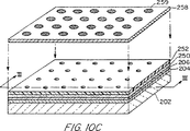
第10C図は、登録が維持される別の実施態様におけるリフトオフ処理中のウェハーの部分の部分斜視図である。
第10D図と第10E図は、リフトオフプロセスにおける付加段階後の第10C図の構造の断面を示す。
第11A〜11E図は、発明によるリフトオフ手順のプロセスフローにおける諸段階中のウェハーの概略図である。
第12A〜12C図は、発明の別の好ましいリフトオフ手順の概略断面図である。
第13A〜13C図は、発明による好ましい転写方法を概略的に示す。
第14A図と第14B図は、発明による付加的な転写方法を概略的に示す。
第15図は、発明によるデバイス登録を監視制御するための好ましいシステムを示す。
第16図は、本発明の高解像度モニターにおいて使用される好ましい映写システムの断面図である。
第17図は、本発明の好ましい高解像度モニターの図である。
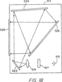
第18図は、折り畳み光学系幾何形状を使用する高解像度映写モニターの図である。
第19図は、第18図のモニターにおいて使用される別の好ましい映写システムの図である。
第20図は、第18図のモニターにおいて使用される別の好ましい映写システムの図である。
第21図は、本発明の像プロジェクタの図である。
第22図は、発明の別の好ましい高解像度映写モニターの図である。
第23図は、本発明の映写デバイスのためのドライバーシステムを示す回路図である。
第24A〜24D図は、光弁マトリックスを作製し、それを支持構造に転写するための好ましい工程及び転写順序図である。
第25A〜25C図は、光弁マトリックスを作製し、それを支持構造に転写するための別の好ましい工程及び転写順序図である。
第26A〜26E図は、マトリックスを作製し、それをガラス基板に転写するためのさらに別の好ましい工程及び転写順序図である。
第27図は、従来のスライドプロジェクタの図である。
第28図は、本発明によるアクティブマトリックススライド組立体の分解斜視図である。
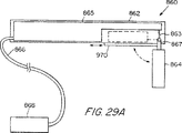
第29A〜29B図は、従来のスライドプロジェクタにおいて使用されるアクティブマトリックススライド組立体の好ましい実施態様を示す。
第30図は、従来のスライドプロジェクタにおいて使用されるアクティブマトリックススライド組立体の別の好ましい実施態様の図である。
第31図は、本発明のアクティブマトリックススライド組立体の別の実施態様の斜視図である。
第32図は、アクティブマトリックススライド組立体のための好ましいドライバーシステムを示す回路図である。
第33図は、本発明のアクティブマトリックススライド組立体のさらに別の実施態様の斜視図である。
第34A〜34B図は、第33図のアクティブマトリックススライド組立体のための2つの好ましいドライバーシステムを示す回路図である。
第35図は、アクティブマトリックススライド組立体のさらに別の実施態様の斜視図である。
第36図は、アクティブマトリックススライド組立体において使用される複数のアクティブマトリックスを設けるために処理される半導体ウェハーの頂面図である。
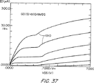
第37図は、キンク効果を示す浮遊体nチャネルMOSFETの電圧特性である。
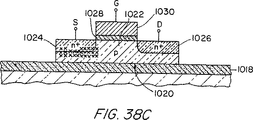
第38A図、第38B図と第38C図は、本発明の打込み手順を示す。第38D図は、第38A〜38C図において提示した方法によって生成されるnチャネル浮遊体MOSFETの別の好ましい実施態様を示す。
第39A図は、本発明による硫黄打込みと硫黄打込みのないデバイスの電圧特性とドレインコンダクタンスを示す。第39B図は、シリコン打込みを使用する発明により作製されたデバイスの電流−電圧特性を示す。
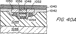
第40A図と第40B図は、ディスプレイパネルにおけるピクセル制御回路として本発明の浮遊体nチャネルMOSFET素子の使用の2つの実施態様を示す。
好ましい実施態様の詳細な説明
発明の好ましい実施態様が、第1図のパネルディスプレイの斜視図において示される。ディスプレイの基本構成要素は、白色又は他の適切な色である光源10と、第1偏光フィルター12と、回路パネル14と、フィルター板16と、第2偏光フィルター17とを含み、これらは層化構造において固着される。液晶材料(不図示)は、回路パネル14とフィルター板16の間の容積に配設される。回路パネル14におけるピクセル22のアレイは、各ピクセルが、ピクセルとカラーフィルター板16に固着した対向電極の間にある液晶材料において電界を生成する如く、アレイに隣接して位置付けられた第1及び第2回路構成要素18、20を有する駆動回路によって個別に作動される。電界は、液晶材料を透過される偏光の回転を生じさせ、その結果、隣接カラーフィルター要素が照明される。フィルター板システム16のカラーフィルターは、青24、緑25、赤27と白29の如く4つのフィルター要素のグループに配列される。フィルター要素24、25、27、29に付随したピクセル又は光弁は、そのピクセルグループに対して所望の色を設けるために選択的に作動される。
他の好ましい実施態様は、各ピクセルの対して光弁を形成するために固体材料の使用を含む。電界発光膜又はその光伝達特性が電界の印加によって変更される任意の材料の如く発光材料が、本発明の光弁を供給するために使用される。
パネルにおけるディスプレイを制御するために使用される駆動回路が、第1B図において示される。回路18は、入り信号を受信し、バス13を通してピクセルに信号を送信する。回路20は、各ピクセルにおけるコンデンサ26を充電する個々のトランジスタ23をオンにするためにバス19を走査する。コンデンサ26は、アレイの次の走査まで、ピクセル電極と液晶21における電荷を持続させる。発明の多様な実施態様は、所望のディスプレイの形式により、各ピクセルでコンデンサを使用する又は使用しない。
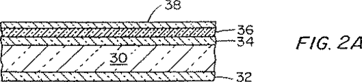
第2A〜2L図は、回路パネル回路構成が形成されるシリコンオン絶縁体(SOI)膜を形成するために、孤立シリコンエピタキシー(ISE)プロセスの使用を示す。なお、任意の数の技術が単結晶Siの薄膜を設けるために使用される。第2A図に示されたものの如くSOI構造は、基板30と、基板30において成長又は堆積された酸化物34(例えば、SiO2等)とを含む。シリコンの薄い単結晶層は、酸化物34上に形成される。酸化物(又は絶縁体)は、こうして、Si表面層の下に埋込まれる。ISE SOI構造の場合に、頂部層は、実質的に単結晶の再結晶化シリコンであり、これからCMOS回路が作製される。埋込絶縁体の使用は、従来のバルク(チョクラルスキー)材料において獲得されるよりも高速のデバイスを設ける。1.5x10⁶超のCMOSトランジスタを含む回路の作製が、ISE材料において為された。
第2B図に示された如く、膜38は、各ピクセルに対するトランジスタ領域37とピクセル電極領域39を規定するためにパターン化される。それから、酸化層40が、各ピクセルの2つの領域37、39の間のチャネル48を含むパターン化領域上に形成される。真性結晶化材料38が、その後、nチャネル素子を設けるためにホウ素又は他のp形ドーパント(又は代替的に、pチャネル素子に対してn形ドーパント)を打込44まれる(第2C図において)。
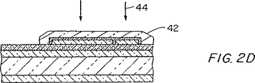
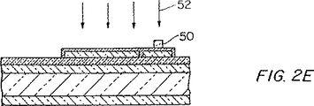
それから、多結晶シリコン層42が、ピクセル上に堆積され、そして層42が、第2D図に見られる如くn形ドーパントを打込46まれ、ゲートとして使用される層42の抵抗率を低下させる。ポリシリコンは、第2E図に見られる如くゲート50を形成するためにパターン化され、続いて、トランジスタに対するp+ソース及びドレイン領域を設けるためにホウ素の大打込み52が行われる。第2F図に示された如く、酸化物54が、トランジスタ上に形成され、そして開口60、56、58が、それぞれ、ソース66、ドレイン64とゲートに接触するために、酸化物54を通って形成される。アルミニウム、タングステン又は他の適切な金属のパターン化メタライゼーション70は、露出ピクセル電極62をソース60(又はドレイン)に連結し、ゲートとドレインを他の回路パネル構成要素に連結するために使用される。
第2作製手順は、ガラスに貼着された処理シリコンの薄い(1〜5ミクロン)膜を形成するための開発された基板リリースプロセスの一つである。これらの膜は、転写の前に部分的又は完全に作製されるFETの如くアクティブ半導体デバイスを含む。転写(CLEFT)アプローチのための横方向成長エピタキシャル膜の劈開を含む結晶化及びリリース手順は、参照としてここに取り入れた米国特許第4、727、047号においてさらに詳しく記載される。化学エピタキシャルリフトオフ(CEL)アプローチは、米国特許第4、846、931号と第4、883、561号においてさらに詳しく記載される。CLEFTとCELの両技術は、基板が消費される他のアプローチと比較して費用の削減につながる基板の再使用を許容する。薄膜リリース技術をSOIウェハーと組み合わせることにより、ガラスにおいて必要な高品質膜及び回路を形成することができる。
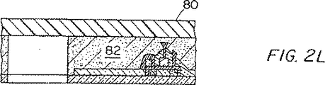
上記は、CELプロセスがリリース層のHF(又は他のエッチャント)アンダーカットのために必要とされる横距離によって制限されることを示す。CELを使用する大領域パネルの鍵は、完全な大領域膜ではなくパターン化デバイス及び/又は回路のリリースである。というのは、回路又はデバイスは、エッチングをリリース層に達するようにするために膜を通った垂直チャネルとして使用される未使用領域を有するためである。このアプローチは、第2H〜2L図において示される。リリース基板から回路を除去するために、第1開口70(第2H図)が、ピクセル間に生ずる層36の露出領域において形成される。層34の第2大部分が、層36の部分が空洞72上に広がる如く空洞72を形成するために除去される。
第2I図において、支持柱76が、空洞72と開口70を満たすために形成され、層36の部分上に広がる。それから開口又はヴァイアホール74は、エッチャントがホール74又は横開口78を通って導入される如く、層36を通して設けられ、層34を除去する(第2J図参照)。残りの絶縁層36と支持された回路構成は、支持柱76により基板30に関して適所に保持される。
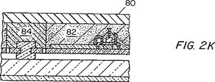
紫外光で硬化されるエポキシ樹脂が、透光性基板80を回路と層36に装着するために使用される。基板80は、柱76の回りのエポキシ樹脂84の領域が未硬化であり、残りのエポキシ樹脂82が硬化される如くパターン化される(第2K図参照)。基板30と柱76は、第2L図に示された構造を設けるために除去され、その後、所望のディスプレイパネルを設けるために処理される。
なお、UV硬化接着剤(又はテープ)が、必要な場合に回路を保護するためにパターン化され、そしてHFが、残りのリリース層に達するために使用される。なお、テープが使用される場合に、テープは、リリース後の回路への支持を設ける。膜を含む大領域GaAsデバイスが、このようにして作製され、そしてこれらは、一つのテープにおける全ウェハーからデバイスを形成するために剥離された。剥離された回路は、液晶表示パネルのガラスと他の要素上に再取付けされる。透明接着剤が、取付けの好ましい方法である。
最終表示パネルを形成するために、第2L図に示された回路パネルは、露出された所望のピクセル要素を残してエッチングされる。絶縁及び位置合わせ層、スペーサー、密封境界と連結用ボンディングパッドが、回路パネルに追加される。画面印刷プロセスが、境界を準備するために使用される。カラーフィルターと対向電極を含む板が、スペーサーの挿入後、密封境界で回路パネルに密封される。ディスプレイは、境界を通っている一つ又は複数の小さな注入孔を介して選択された液晶材料を注入される。それからこの注入穴は、樹脂又はエポキシ樹脂で密封される。第1及び第2偏光器膜又は層が、両側に貼着され、そしてコネクタが追加される。最後に、白光源114又は他の適切な光源が、偏光器112に結合される。
生ずるデバイスの断面図が、第3図に示され、この場合ピクセル電極102と104は、相互に横に離間される。各ピクセル102、104はトランジスタ106と、関連したカラーフィルター120、122を有する。偏光要素112、118は、ガラス又はプラスチックの如く、ボンディング要素又は接着剤108と透光性基板110を含む構造の対向側に位置付けられる。層108は、2〜10ミクロンの厚さを有する透明エポキシ樹脂又は低温ガラスである。
CLEFTプロセスは、再使用可能なホモエピタキシャル基板から化学蒸着(CVD)により成長された薄い単結晶膜の分離を許容する。CELプロセスと異なり、CLEFTプロセスにおいて、回路又はデバイスは、まず、ガラスに貼着され、そして取付けの後、回路と基板の間の分離が行われる。
CLEFTによって基板から除去された膜は、低欠陥密度の本質的単結晶であり、ほんの数ミクロン厚であり、そして結果的に、回路パネルは、小重量で、良好な透過特性を有する。本出願の目的のために、用語「本質的単結晶」は、多数の結晶が、少なくとも0.1cm2、好ましくは0.5〜1.0cm2以上の範囲において膜の平面における断面領域上に広がる膜を意味する。
米国特許第4、727、047号において示されたCLEFTプロセスは、次の段階を係わる。リリース層(虚弱平面)上の所望の薄膜の成長、メタライゼーションと他の被覆の形成、膜とガラスの如く第2基板(又は上層)の間の貼着の形成、及び劈開による虚弱の組込平面に沿った分離である。それから、基板は、再使用のために利用される。
CLEFTプロセスは、リリース層の頂部に連続膜を形成するために横エピタキシャル成長を使用して本質的単結晶材料のシートを形成するために使用される。シリコンに対して、横エピタキシーは、ISEプロセス又は他の再結晶手順によって達成される。代替的に、他の標準堆積技術が、必要な薄膜の本質的単結晶材料を形成するために使用される。
リリース層を形成する材料の必要な特性の一つは、層と半導体膜の間の接着力の欠如である。弱い平面はリリース層によって生成されるために、膜は、劣化なしに基板から劈開される。リリース層は、Si3N4とSiO2の多層膜を具備する。そのようなアプローチは、CMOS論理の裏面を皮膜保護するためにSiO2の使用を許容する。(Si3N4は、虚弱平面を生成するために溶解される層である。)CLEFTアプローチにおいて、回路は、まず、ガラス又は他の転写基板に貼着され、それから、分離され、UV硬化テープと比較して単純な取扱いとなる。
ISEプロセスにおいて、酸化膜は、基板と回路を含むSi膜上に強力に付着される。この理由のために、貼着の強度を化学的に縮小することが必要である。この技術は、リリース層において虚弱平面を形成するために、完全な分離なしに、エッチャントで優先的に溶解されるリリース層に係わる。それから、膜は、ガラスが回路と電極に貼着された後に、機械的に分離される。
機械的分離は次の如く達成される。膜の上面が、ガラスの如く上層に透明エポキシ樹脂で貼着される。それから、膜とガラスが、劈開支持部として役立つ約5mm厚のガラス板に対してワックスで貼着される。金属くさびが、表面を離隔させるために2つのガラス板の間に挿入される。マスクは基板に対して低接着力を有するために、膜は、基板から劈開されるが、ガラスに取付けられたままである。それから、基板は、CLEFTプロセスの別のサイクルに対して使用され、デバイス処理が、膜の背面において完成される。デバイスは上層に付着されているために、裏面側は、写真平版を含む標準ウェハー処理される。
方法は、さらに、Si基板の場合にシーディングにより、異基板の場合に対してシーディングのない単結晶膜の準備に係わる。シーディングされたSi膜の場合に、標準再結晶化プロセスが使用される。いずれにせよ、底面酸化物又は窒化物層が、リリース目的のために最適化される。
第4図に概略的に示された再結晶化システムの一つの実施態様において、基板温度は、下方加熱器130によって融点近くまで昇温される。それから上方ワイヤ又は黒鉛条片加熱器132が、試料134の頂部を走査し、移動するメルトゾーン136を再結晶化させ、又は多結晶シリコンをさらに結晶化させる。Siにおける標準プロセスにおいて、横エピタキシーは、下方酸化物を通った小開口からシーディングされ、そして生ずる単結晶膜は基板の配向を有する。キャッピング層138は、結晶化の前に多結晶材料上の堆積される。
異基板の使用は、シーディングを除外する。この場合に、本質的単結晶Siが、結晶粒界エントレインメント技術によって獲得される。結晶粒界エントレインメントは、再成長領域において熱勾配の変調を導入するために、リリース酸化物又はキャップ層のいずれかをパターン化することにより使用される。温度場におけるこの変調は、メルト前線の位置を変化させ、そして予測可能な位置において境界を連行する。リリース酸化物142のパターン化が、第5A図に示される。この実施態様において、基板140は、リリース酸化物142を充填させた溝150を有する。キャップ146とリリース層142の間に広がる結晶化材料144における境界148のエントレインメントのために、Si回路又は電極は、高品質の領域において位置する。メタライゼーションと他の特徴は、亜粒界上に位置する。
図示された如く、好ましい技術は、必要なエントレインメント構造を有する再使用可能な基板をパターン化することである。いったんこのようにパターン化されたならば、再使用可能な基板は、再パターン化を必要としない。そのようなスキームにおいて、エントレインメント用溝は、溝を完全に充填するために十分な厚さの材料を設けられる。溝における材料は、例えば、プレーナ化Si3N4を具備し、リリース層は、SiO2の一層の堆積を具備する。代替的に、溝は、SiO2で完全に充填される。それから、溝はリリースエッチングのためのチャネルとして機能する。
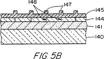
第2アプローチは、第5B図に示された如く、キャップ堆積の後にキャップ層145をパターン化することを含む。キャップ145のパターン化隆起147は、キャップ145とリリース層141の間にある再結晶化材料における境界148に重なる。第3アプローチは、多結晶シリコン層をパターン化するものである。キャッピング層は、異基板で使用される。キャッピング層は、熱サイクルを通して粘着性でなければならないが、デバイス処理のために除去可能でなければならない。キャップは、滑らかなSi基板に対して十分に作用するが、エントレインメントのために必要なパターン化層は、新しい膜を必要とする。
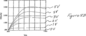
第6〜8図は、ガラス基板への転写の前後の発明により作製されたMOSFETの電気特性を示す。第6A図は、直線領域においてデート電圧VGの関数としてドレイン電流IDと相互コンダクタンスGMをグラフで描き、この場合ドレインソース電圧は、ガラスへの転写の前のMOSFETに対して50mVである。MOSFETは、250μm/20μmの幅対長さ比と、0.5μm厚再結晶化シリコン材料において890Åのゲート酸化物厚を有する。第6B図は、ガラスへの転写の後の同一デバイスのドレイン電流IDと相互コンダクタンスGMを示す。
第7A図は、2つのドレインソース電圧VDS=50mVとVDS=5Vにおいて対数スケールにおいてプロットされた第6A図のデバイスのドレイン電流をグラフで示す。
第7B図は、ドレインソース電圧VDS=50mVとVDS=5Vにおいて対数スケールにおいてプロットされた第6B図のデバイスのドレイン電流をグラフで示す。
第8A図は、VGS=0、1、2、3、4と5ボルトのゲート電圧において第6A図のデバイスのドレインソース電圧の関数としてドレイン電流IDをグラフで示す。
第8B図は、VGS=0、1、2、3、4と5ボルトのゲート電圧において第6B図のデバイスのドレインソース電圧の関数としてドレイン電流IDをグラフで示す。
CELアプローチに対して、一層の実施態様は、ガラス板における剥離回路の再取付けに係わる。塗布方法は、薄膜半導体と接着剤の間の一様な密着を保証するが、薄膜において亀裂が入ってはならず、又は他の欠陥を導入してはならない。
方法は、分離される層の前面側に対するアピエゾンワックスの塗布に係わる。ワックスにおける応力は、湾曲を引上げ層に伝え、これにより、エッチング前面へのエッチング流体の接近を許容する。エッチング前面への接近は、リフトオフされる全領域の外縁からのみ達成される。
このプロセスは、2cmx2cmよりも大きな領域に対して数時間又は数日までにわたる長いリフトオフ時間のために、大領域リフトオフに係わる応用のために限定的使用となる。湾曲は、エッチング前面へのエッチャントの接近を増大するために必要とされる。もし、リフトオフのために必要とされる湾曲は、低温ワックスによって生じ、その結果、このワックスが存在する間、高温処理は行われない。本試料は、しばしば、サイズに劈開され、基板再使用を許容しない。ワックス塗布プロセスは、自動化され、この手順が好ましい応用において基板再使用を許容するためにパターン化される。このプロセスは、裏面処理を必要としない個別の小領域に対してのみ使用される。
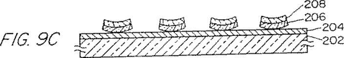
本発明の別の実施態様は、標準リフトオフプロセスにおいて黒ワックスに置き換わるために、種々の膨張係数を有する薄又は厚膜材料の組み合わせを使用することに係わる。このプロセスは、第9A〜9C図において示される。正しい温度を使用することにより、リフトオフのために必要とされた湾曲は、層における差分応力により達成される。単一層は、リフトオフされる材料に関して正しい膨張係数を有するならば使用される。この方法は、リフトオフ温度において正しい湾曲を伝え、室温において平坦であり、裏面処理中膜を支持する支持層を許容する。
本発明のこの実施態様を第9A〜9C図の構造200に関連して以下に記載する。エピタキシャル層又は素子が形成される任意の適切な基板材料を具備する基板202が、設けられる。リリース層204は、基板202上に、好ましくはCVDにより成長される。薄膜シリコンリリース可能層に対して、SiO2層が、前述の如く使用される。
半導体層構造206は、同様に、CVD又は他の前述の方法によりリリース層204上に形成される。構造206は、好ましくは、発明によりトランジスタのアレイの作製のために配置された材料を具備する。
例えば、CVDを使用することにより、構造206は、非常に薄く、すなわち、約5ミクロン未満、好ましくは、2ミクロン未満にされ、接触層は0.1ミクロン厚未満にされる。
必要なドーパントは、一般に、ソース、ドレイン及びチャネル領域を規定するために成長プロセスの後、拡散又は打込みにより導入される。次に、構造206は、ゲートと金属接点を形成するために従来の技術を使用して、前面又は頂面側において処理され、この場合各ピクセスは、必要に応じて、バスバーとボンディングパッドを配置される。
第1リフトオフ実施態様において、被覆208は、前面側処理構造206において形成される(第9A図)。被覆は、異なる熱膨張係数を有する厚又は薄膜材料の組み合わせから成る。例えば、被覆208は、窒化物、金属、バイメタル又はガラス応力被覆を具備する。接触メタライゼーション(不図示)がまた、接触層上にこの時点において塗布される。
被覆層208と構造206は、従来の写真平版を使用してパターン化され、そして被覆材料208と構造206は、適切な選択エッチャントによるエッチングにより、第9B図に示された如くリリース層204まで所定領域において除去される。上記の段階は、被覆208の被覆材料の間に大きな熱応力が生じないほど十分低い所定温度において行われる。次に、温度は、十分な温度まで上昇され、被覆208において熱応力を生じさせる。この上昇された温度にある間、構造はリリースエッチャントに露呈される(第9C図参照)。
リリースエッチャントは、究極的に、被覆208によって支持された分離素子構造206を除去させるためにリリース層204を十分にエッチングする。それから、これらの構造は、低温にされて熱応力が軽減され、続く裏面処理のために個別素子を平坦にしておく。
このプロセスは、個別チップを裏面処理のために平坦にさせ、支持構造が、裏面処理温度に不浸透性のガラスの如く材料から形成されることにおいて、Gmitter他の黒ワックスプロセスに対するかなりの利点を設ける。
2つの異なる手順は、ウェハースケールリフトオフを達成するために使用される。第1の方法は、転写される膜が形成される全基板のエッチングに係わる。これは、「エッチバック」手順と呼ばれる。
第2の方法は、ウェハー又は試料の縁のみからリリース層に接近し、一つの大形シートとして材料を剥離する。この第2の方法は、同一ウェハーから引き上げられた素子の間の登録を必要としない場合である。登録が望まれないならば、自動化手順が、個別素子の大領域又は材料の領域のリフトオフのために使用される。前面側処理が完了した後、UV硬化エポキシ樹脂が、所望のパターンで硬化され、非所望の部位を除去され、それから、リリース層までエッチングするためのマスクとして使用される。それから、UV硬化エポキシ樹脂は残され、分離の後に引き上げられた膜のための支持部として作用する。個別素子は、エッチング溶液から回収され、選出及び部位形式方法を使用して個別に処理される必要がある。
これらの代替リフトオフプロセスが、第10A〜10E図を参照して以下に記載される。この場合第9図における対応項目は、第10図の同一参照番号を保持する。第10A図の部分斜視断面に示された如く、基板202は、その上にリリース層204と、続いて、素子構造206を形成し、すべては第9図に関連して記載された如くである。構造206へのボンディングパッドと金属接点(不図示)の如く全前面側処理は完了される。
溶解性でない又はエッチング可能でない状態からより溶解性又はエッチング可能な状態(又はその逆)へ変形される材料が、前面側処理構造206上に形成される。例えば、UV硬化性エポキシ樹脂230が、構造206上に広げられる。このエポキシ樹脂は、UV光への露出により非溶解性になる特性を有する。
それから、材料のUV透光マスクリリース層232が、エポキシ樹脂230上に形成され、そして開口236を具えるパターン化不透明マスク234が層232上に添着される。
マスク234は、UV光を照射され、マスク開口236の下側のエポキシ樹脂の領域を硬化させ、未硬化状態におけるよりも非溶解性にする。リリース層232が除去され、そしてマスク234が除去される。次に、未硬化エポキシ樹脂は、リリース層204までの如く、溶剤によって除去される(第10B図参照)。
硬化エポキシ樹脂230は、リリース層204からの分離の後、薄膜構造206のための支持部として役立つために構造上残される。このようにして、エッチング前面は、チャネル240をリリース領域204まで切込むことにより、構造206の全上面領域を小領域に分割することにより増大される。
ウェハーサイズリフトオフのための第2の方法は、引き上げられる全領域を小領域に分割することにより、エッチング前面の量を増大させることによる。チャネルは、引き上げられる材料の全領域に切込まれ、これにより、リリース層を露出させる。これらのチャネルは、領域を完全に分離し、又はリフトオフ領域へ部分的に切込むスリットから成る。
第2の方法は、露出リリース層へのエッチング媒体のより大きな接近を許容しながら、相互に関して材料の小領域を登録することを試みる問題を扱う。これを行う能力は、溶液からの容易な回収、裏面側におけるウェハースケール処理、及びエッチング前面の小領域と最大露出による短いリフトオフ時間を可能にする。このアプローチの重要な特徴は、すべてのエッチング前面にエッチング溶液の接近を設けながら、全ウェハー領域の登録を可能にすることである。
素子間の登録がトランジスタのアレイにおける如く、必要とされる場合に、第10C〜10E図の代替実施態様のリフトオフ方法は多数の利点を設ける。
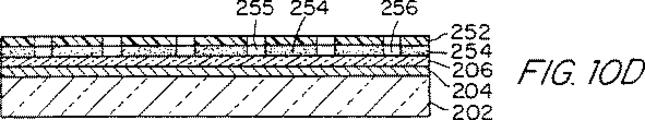
第10C図のこの代替プロセスは、露出リリース層へのエッチング媒体の接近を許容しながら、相互に関して材料の小素子又はピクセル領域を登録することを試みる困難な問題を解決する。これを行う能力は、溶液からの容易な回収、裏面側におけるウェハースケール処理、および小領域と最大エッチング前面による短いリフトオフ時間を可能にする。このアプローチはまた、全エッチング前面にエッチング溶液の接近を設けながら、全ウェハー領域を通じて素子の登録を可能にする。第10C図は、ウェハーの矩形部分区分を示す。ウェハーは、半導体基板202と、その上にCVDによって堆積されたリリース層204と、その上の前面処理トランジスタパネル206とから形成され、これらはすべて前述の如くである。
未硬化液体UVエポキシ樹脂250の如く変形可能な材料は、構造206の頂面又は前面に広げられる。前実施態様に関する離脱点は、プラスチックの如く透明材料から作られた穿孔プレーナ格子252がエポキシ樹脂250の頂部に位置合わせされる時、次の段階において行われる。穿孔256は、格子252の平面に直交し、かつ貫通する。
穿孔256を覆うために位置合わせされた不透明円256を具えるフォトマスクが、格子252上の添着される(第10C図)。(オプションのUV透過性マスクリリース層(不図示)が、マスク除去を容易にするためにマスク258と格子252の間に形成される。)UV光は、マスク上に集束され、第10D図に示された如く、不透明円256の下を除いてすべての下側エポキシ樹脂254を硬化させ、この場合エポキシ樹脂250の硬化区分は、影つき区分において示され、未硬化区分は空白である。マスク258は除去される。未硬化エポキシ樹脂250は、適切な溶剤によって開口256から除去され、そして構造206が、開口を通してリリース層204までエッチング除去される。それから、リリース層は、上記の如く、開口256を使用してエッチング除去される。エッチャントの接近が、こうして、ウェハーでの多数の点において達成され、硬化エポキシ樹脂254によって格子252に付着されたアレイを生ずる(第10E図参照)。
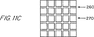
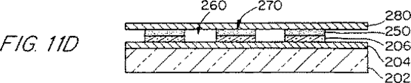
登録への別のアプローチは、リリース204までエッチングすることにより、素子材料において直接にチャネル260を形成し、これにより、材料のみにおいてチャネルを形成するものである(第11A図)。これらのチャネルはまた、第9図のUV硬化エポキシ樹脂パターン化方法を使用してより高くされ、それから、リリース層204までエッチングする(第11B図参照)か、あるいは任意の他の方法により、第11C図の平面図に示された如く分離される領域270の間にチャネル260又は接近路を形成する。それから、支持部280が、チャネル260上の材料270に付着され、そしてエッチャントが、チャネルに沿って走らされ、これにより、ウェハーの中央へエッチャントを接近させる(第11D〜11E図)。より高いチャネルは、高速リリースを達成するために、毛細作用を加速する補助をする。真空補助、超音波補助等を含む他の方法が、チャネル260によるエッチャントの移動を加速するために使用される。
同一線に沿って、チャネル260が、下のリリース層を露出させるために素子材料において作製される。それから、多孔性材料が、スピンオンされ、あるいは前面に形成又は付着される。この材料は、UV、熱、又は溶剤処置等によって硬化された時、剛性又は半剛性であり、そしてこのため、基板からの分離の後、引き上げられた膜を支持することができる。材料は、エッチャントによって攻撃されることなく、エッチャント流体を通過するために十分に多孔性である。このようにして、エッチャントは、多孔性材料を通過し、そしてその露出点においてリリース層にの接近を与えられる。
別の実施態様において、リリース層エッチャントが、下側支持構造が構造206に付着される前に、リリース層と接触される。このプロセスが作用するために、チャネル260は、エッチャントがトラップされるために引き上げられる素子又は材料の領域の間に形成されなければならない。基本プロセスは、次の如くである。チャネル260は、基板202においてリリース層204を露出させるリフトオフ領域206の間に形成される。これは、素子間にチャネルを生成する前述の方法のいずれかにより行われる。非常に良好に作用する単純方法は、フォトレジストマスキングにより材料206に直接にチャネルを形成し、続いて、リリース層204までエッチングするものである。これは、リリース層上の材料の高さに等しい高さのチャネル260を材料において形成する。次に、エッチャントが、引き上げられる層の表面に配され、あるいはウェハーがエッチャントに沈められる。いずれにせよ、引き上げられる領域206の間のチャネル260は、エッチャント材料で充填される。これが行われた後、リフトオフの後登録を保持する上側支持層が、ここで詳細に記載されるボンディング方法により構造206の前面に添着される。上側支持部は、材料206に固着され、一方、ウェハーは沈められ、あるいはエッチャントがウェハーの前面を覆い、チャネルを充填する。支持材料は、形成されたチャネルを満たさず、これによりエッチャントを押し出さないほど十分に剛性でなければならない。適切な支持材料は、ガラス、プラスチック又は他の透光基板を具備する。これは、エッチャント接近ホールを必要とせず、こうして、プロセスを非常に単純化する固体支持媒体を許容する。
トラップされたエッチャントは、薄膜領域206が、後の処理、すなわち、裏面導体メタライゼーションとボンディングパッドの形成ために、裏面を露出させて、支持部によって支持及び登録される間、除去される如く、リリース層204を十分に溶解する。
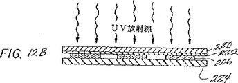
上記の支持材料のほかに、小形素子を取扱うために産業において非常に公知のUVリリーステープは、幾つかの理由のために優れた支持部の選定であることが立証された。これらのテープは、強いUV放射線に露出された時、接着力の大部分を失うという性質を有する。さらに、湿気は接着剤に影響を与えることはなく、液体に浸されても、極めて良好に塗布される。これらのテープは、単独で又は肥厚支持物と結合して使用される。この付加的な支持物は、永久的でないならばUV放射線を透過する材料から形成され、使用されるエッチャントによって攻撃されてはならない。
UVリリース接着剤は、テープ裏当て材の代わりに、他の支持材料に直接に塗布される。第12A〜12C図に示された如く、両面UVリリーステープ282と組み合わされた支持物280が使用できる。テープ282の一方の側面が、支持物に接着される。それから、他方の側面は、エッチャントが塗布された後、構造206の前面に接着される。エッチャントは、それから、素子206をアンダーカットさせる。それから素子は、第12A図に示された如く、支持物280にリリーステープによって付着される。リフトオフ時間は、エッチャントがウェハー表面における多数の点からリリース層に接近するために、非常に短い。
このようにして、素子は、相互に関して登録され、裏面処理中、支持物280によって支持される。
それから、テープの接着力は、支持物を通したUV照射によって緩められ(第12B図又は第12C図)、そしてテープは、素子をなお付着したまま、キャリア280から取り除かれる。一層のUV露光は、素子を真空棒によって除去させ、テープ288から基板288(第12B図又は第12C図参照)又は他の媒体を具える任意の他のテープ284又はエポキシ樹脂286に直接に転写させるために十分な程度にまでテープへの素子の接着力を減少させる。0.5cm幅の個別領域が、この非湾曲方法によって引き上げられた。同時に引き上げられ登録される全ウェハーサイズは、ウェハーサイズによってのみ制限される。
示された如く、代替態様は、UV硬化接着テープ及びエポキシ樹脂の使用に係わる。接着剤は、薄膜トランジスタとCMOS回路要素をガラスに貼着するために使用される。接着剤は、14”x14”以上の板に塗布される。塗布方法としては、スピンコーティング、蒸気コーティング、スプレー、及び必要な一様性と光学品質を設けるための標準厚膜塗布プロセスがある。
別の好ましい実施態様は、回路パネルにおいて粗に離間した位置に密に配置した素子を転写する方法を含む。第13A図、第13B図と第13C図に示された技術は、素子が正しく位置付けられるまで、伸縮性テープ又は膜の伸張又は収縮を使用する。この技術はまた、前述のリフトオフ手順と機械的又は伸縮及び機械的方法の組み合わせを含む。市販される素子は、膜の伸張を正確に制御するために使用される。多様な方法が、構成部品の適正な登録を設けるために、伸張と転写中素子の間隔を測定するために使用される。
構造300と関連して第13A図に示された如く、トランジスタ又は薄膜半導体領域304のアレイが、伸縮性基板302に転写された。トランジスタ又は領域304は、上記の手順により、あるいは任意の他の適切な手順を使用して作製及び転写された。基板302は、接着剤を具備する。
第1実施態様において、構造は、第13B図に示された如く軸306に沿って引伸ばされ、これにより、別の方向における素子間の距離310を同一にしながら、軸306に沿った素子304間の距離308を増大させる。それから、基板302は、第13C図において示されたアレイを生成するために、軸314に沿って引伸ばされる。この場合素子304は一方の方向において間隔308を有し、直交方向において間隔312を有する。
別の実施態様において、第13A図の構造300は、第13C図に示されたアレイを生成するために、方向306と314において同時に引伸ばされる。
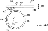
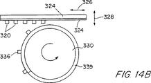
機械的技術が、第14A図と第14B図において示される。テープにおける素子320のリフトオフアレイから開始する。このテープ322は、軸326に沿って進退し、軸328に沿って上下移動するフレーム324に据え付けられる。ドラム330は、その周囲の回りにたわみ性テープ334を配置される。それから、器具340が、デバイス324上に押し出され、デバイスの第1行をドラムテープ334に押し出す。ドラムテープ334は、必要な角度で方向332において割り出され、そして再び、器具340は、間隔338を有するデバイスの第2行をテープ334に押し出す。これは、すべての行が転写されるまで続く。それから、デバイス336の行を有する第1ドラムテープ334が、フレーム324に据えられる。同一動作は、行を新ドラムテープ339に転写することにより続く。
別の実施態様は、テープを一方の方向において引伸し、これを別のテープに転移し、そしてそのテープを他の方向において引伸し、素子を最終支持物に転写するものである。この方法は、小形個別素子に良く適する。
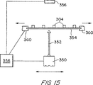
転写又は最終基板における素子304間の距離を測定するためのシステムが、第15図に概略的に示される。レーザー350は、ビーム352を基板354の方向に向け、源を走査する。センサー356は、透過及び/又は反射光を検出し、かつ、ビームが素子304によって偏向される場合に信号を発生するように位置付けられる。コントローラ358は、素子304間の距離が正確に測定される如く基板354に関してビーム352の移動を相関させる。コントローラ358は、調整が素子の選択行又は列の間隔に為される如く、引伸し機構360に電気的に連結される。
引伸し機構360は、基板354が付着されたカラーを通して押圧されるピストンから成る。基板354に対向しカラーを通ったピストン面の移動は、素子304間の間隔を増大させるために正確に規定された方法で基板354を引伸す。代替的に、その周囲に沿って基板を把持し、適切な方向において基板を正確に引張る第15図に示されたものと同様の市販される引伸し機構がある。
引伸しの後、登録された素子は、光弁(LCD)作製のためのガラス、ポリエステル又は他の適切な基板に転写される。代替的に、素子は、ディスプレイ作製のために発光デバイスに取り付けられる。
本発明の別の好ましい実施態様において、第16図に示された映写モニターがある。映写モニターは、映写スクリーン、鏡又はレンズである拡大表面514に究極的に向けられる多色像を生成する映写システム500を含む。映写システム500から表面514への直接の経路が第16図に示されるが、好ましい実施態様において、映写システムから出力された像は、表面514に映写される前に、光学幾何形状を通過される。冷却が、ファン又は適切なヒートシンクによって設けられる。
プロジェクタ内で、ハロゲン灯502からの光が、反射器505と集光レンズ503によってダイクロイックミラー504の交差対へ向けられる。集光レンズ503は、好ましくは、+X方向において発せられた光を集光するために最大集光効率のために設計される。球面反射器505は、−X方向において発せられた光を集め、灯の光をそれ自身に結像する。
灯502からの白光は、赤、緑及び青の原色部分に光を分離する交差ダイクロイックミラー504に向けられる。光の分離色は、3つの液晶光弁マトリックス508の各々の裏面508aを照明するために隣接鏡506によって指向される。本発明により、各光弁マトリックス508は、トランジスタのアレイと、電極のアレイと、偏光器と、カバーガラスと、実質的単結晶のシリコンの薄膜及び光が(以下に詳細に記載される)表面514に選択的に透過される隣接液晶材料において形成したドライバーとを具備する。
各光弁マトリックス508は、照明光がマトリックスの前面508bにおいてそれぞれの原色における像を形成するために液晶材料を選択的に透過される如く、個々の光弁を変調するためのドライバー回路によって制御される。それから、3つの原色像が、ダイクロイックプリズム510によって単一多色光ビームに光学的に結合される。光ビームは、映写レンズ512によって表面514に映写される。
別の好ましい実施態様において、映写システムは、拡大表面に映写される単色光ビームを生成するように変調された単一光弁マトリックスを使用する。さらに別の好ましい実施態様において、各光弁マトリックスは、光が表示用視野表面に選択的に透過される強誘電性材料を使用する。
好ましい映写システムが3つの光弁マトリックスと特定の内部光学幾何形状に関して記載されたが、好ましい実施態様は、多様な内部光学幾何形状で構成された一つ以上の光弁マトリックスを含む。例えば、一つの好ましい実施態様において、高精細複合像が、個々の光学系を配置した4つ以上の光弁を有する映写システム520において生成される。第19図を参照すると、4つの光弁マトリックス521は、各々、NxNピクセルアレイを設ける。各光源523からの光は、それぞれのマトリックス521の裏面521aを照明するために向けられる。各光弁マトリックスは、照明光がマトリックスの前面521bにおいて像を形成するためにマトリックス内の液晶材料を選択的に透過される如く、個々の光弁(又はピクセル)を変調するための駆動回路(不図示)によって制御される。なお、各マトリックス521は単色又は多色像を生成することができる。
好ましくは35mm光学系と互換性の各像は、それぞれのレンズ525に向けられる。各レンズは、表面529の部分に映写される光ビーム527を設ける。それ自体、各マトリックスは、複合像の像セグメントを設けるように構成される。この構成を使用して、Nx4Nのピクセル密度を有する複合高精細像が生成される。それから、複合像は画面に表示され、又は表示用光学幾何形状を通して指向される。
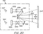
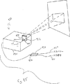
別の好ましい実施態様において、一対の光弁マトリックスが、高精細像を設ける映写システムにおける光学配置で使用される。第20図を参照すると、一対の光弁マトリックス533と535が、映写システム531に位置付けられる。光源537からの光は、それぞれのマトリックスの裏面を照明するために向けられる。各マトリックス533と535は、駆動回路(不図示)によって制御され、そして単色又はカラー像を生成する。各マトリックスの前面側に形成された像は、それぞれのレンズ系に向けられる。さらに具体的には、マトリックス533によって生成された像は、集束レンズ539によって一対の鏡541と543に向けられる。像は、鏡541とともに別の鏡543から反射され、そして表面547の中央領域545に映写される。同様に、マトリックス535によって生成された像は、レンズ549と550によって鏡552と543に向けられる。しかし、鏡552は、鏡552と鏡543から反射された像が表面547の大領域554に映写される如く配置される。鏡543からの2つの反射像は、表面547において高解像度中央領域545と低解像度周辺部554を生成するように結合される。
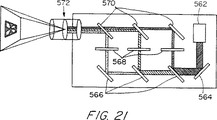
本発明の原理を使用する像プロジェクタ560が、第21図に示される。プロジェクタは、像を視野表面(不図示)に映写するためのズーム又は可変集束レンズ572を使用する。ズームレンズ572を単純レンズと置き換えることにより、プロジェクタ内の映写システムは、第17図のモニターにおいて使用される。第21図の映写システムは、光を指向させるためにさらに別の光学構成を使用する。灯562からの白光は、鏡564から反射され、3つにダイクロイックミラーに向けられる。光の分離色は、3つの液晶光弁マトリックス568の裏面を照明するために鏡によって指向される。ドライバー回路(不図示)によって制御される各マトリックスは、マトリックスの前面側においてそれぞれの原色の像を形成するために光を選択的に透過させる。3つの原色像は、ダイクロイックミラー570を介してレンズ572に向けられる。レンズは、像を単一多色光ビームに結合する。
第17図を参照すると、映写モニター515は、プロジェクタからスクリーン518へ光ビームを向けるための光学配置を含む。その目的のために、映写システム500は、単色又は多色光ビームを鏡516に映写する。鏡は、鏡からの反射光が視準される如く、映写システムに関して傾斜して位置付けられる。視準光は、大視野スクリーン518の裏面に向けられる。それ自体、像は、スクリーン518の前面において見られる。
本発明の原理を取り入れる別の映写デバイスは、第22図に示された映写モニターである。例示の目的の簡易性のために、単一光弁マトリックスと支持光学系幾何形状が示される。しかし、好ましい実施態様は、支持光学系幾何形状を各々有する複数の光弁マトリックスを含む。第22図を参照すると、光源578は、レンズ580によって鏡582に向けられる白光を発生する。ダイクロイックミラー582は、白色を単一原色に分離し、色光を光弁マトリックス584に向ける。光は、像を形成するマトリックスを選択的に透過され、像はレンズ585によって鏡の折畳み光学配置に向けられる。それ自体、像は、第1鏡586に向けられ、次に第2鏡588に向けられる。第2鏡は、その反射光が視準される如く位置付けられる。視準された単色像は、他の単色像と結合され、そして合成視準像は、大形視野スクリーン590の裏面に向けられる。それ自体、高精細像が、スクリーンの前面において見られる。
本発明の原理を取り入れるさらに別の映写デバイスは、第21図に示された独立型プロジェクタである。前述の如く、プロジェクタ560は、複数の単結晶シリコン光弁マトリックスと高精細カラー(又は単色)像を生成するための光学幾何形状を使用する。合成像は、視野表面又はスクリーンの前面又は背面に映写可能な像ビームを形成するためにズーム又は可変焦点距離映写レンズ572を通って指向される。前実施態様における如く、プロジェクタは、35mm光学系と互換性でありながら、高精細像を設ける。
映写表示デバイスの好ましい実施態様は、一つ以上の光弁マトリックスを駆動するためのドライバー回路を含む。第23図を参照すると、アクティブマトリックス600は、共配置されたドライバー回路構成(第1B図参照)によって個別に作動される複数の光弁を具備する。共配置されたドライバー回路構成は、ビデオ条件回路602と、システムクロック604と、オプションの振幅対パルス持続時間(APD)コンバータ606と、列ドライバー608と、行ドライバー610とを含むドライバー回路をサポートすることにより制御される。
ビデオ条件回路602は、RGB信号、NTSC信号又は他のビデオフォーマット信号、若しくは任意のデジタル又はアナログ信号であるビデオ出力信号を受信する。条件回路は、各原色に対して(ライン611、612と613における)個別ビデオ出力信号を生成する入り信号と、列及び行ドライバー608と610に対する(ライン615における)同期化信号とを処理する。ライン611におけるビデオ入力信号は、データ流の各信号の振幅が各光弁を通過させた光の強度を決定するシリアルデータ流である。
APDコンバータが使用されないならば、ライン615におけるシリアルデータ流615は、行ドライバー610によって受信される。行ドライバー610は、各信号データ流をバス618を通して光弁に送信する。列ドライバーは、ライン615において同期信号を受信し、同期信号に応答して、個々のトランジスタをオンにするためにバス619を通して送信し、データ流の関連信号をして各ピクセルにおけるコンデンサを充電させる。コンデンサは、アレイの次の走査まで、光弁における関連信号の振幅に比例する電荷を持続させる。
代替的に、ADPコンバータは、ビデオ出力データ流の各信号が、信号の振幅に比例するパルス幅を有するパルスに変換される如く使用される。いずれにせよ、ドライバー回路は、前述と同様にして動作する。
本発明の映写表示デバイスは、次に示す広範囲の現コンピュータフォーマット必要条件のいずれをも満足するピクセル密度を有する光弁マトリックスを使用する。

本発明の一つの特徴は、単結晶光弁マトリックスを使用する映写デバイスが高精細像を設けることである。高精細像は、高密度光弁アレイが単結晶シリコン膜において形成されるために可能である。表1を参照すると、光弁対角面がいろいろなアレイサイズとピクセル密度に対して示される。なお、アステリスクを伴う対角次元は、アレイが35mm光学系と互換性があることを示す。
35mm光学系の使用は、光弁像設計次元が42mm(1.654インチ)以内であることを必要とする前記の光学系の大きさ、重量及び費用を最小にすることにおいて重要な特徴である。このため、最高密度の情報内容を設ける光弁結像技術を使用することが望ましい。
ここで議論された光弁技術は2000ドット/インチの作成密度と互換性があると考えられる。これは、小形で、低費用かつ広範囲に利用可能な光学構成部品を使用して高精細像の映写を許容する。小形の光弁は、小形フォーマット集光レンズ組立体、ダイクロイックミラー、プリズム及び映写レンズの使用を許容する。続いて、記載されたプロジェクタとモニターのパッケージサイズは、小次元に維持され、構成部品重量も同様に最小化される。適切な35mフォーマット光学構成部品が、広く利用され、大形及び/又はカスタム光学構成部品に関して低費用で獲得される。35mm互換光弁で満たされないプロジェクタ及びモニター必要条件に対して、より大形の従来又はカスタム光学構成部品が使用される。記載された光弁技術によって与えられた特定光弁フォーマットの最小サイズのために、類似の費用、サイズ及び重量の利点は、カスタム光学構成部品の調達に変容される。
前述の如く、ここで記載された光弁技術は、35mmフォーマット光学構成部品を使用して、1024x768ないし2048x2048ピクセルの映写アレイを実現するために使用される。これは、比較的小形の次元と低重量において高精細カラー及び単色像プロジェクタ及びモニターの実行を許容する。
モニターの一つの実現は、データ窓接近のために付加的なスクリーン余地のある2つの併置8.5インチx11インチページのディスプレイのために適する17.5インチx11.5インチ像を形成するものである。前述の光弁及び映写技術の使用は、モニターの物理フォーマットを22インチ高以下、20インチ幅以下、及び10インチ深以下にすることができる。この実現における単一の150〜300ワット金属ハロゲン灯の使用は、25フィートランバート以上の輝度において後方伝搬スクリーン像を設ける。スクリーン材料の選定は、最大視野角のための単純拡散器又は縮小立体視野角での最大輝度のためのレンズ構成を含む。
第24B図を参照すると、前述の技術のいずれかの如く集積回路処理技術が、単結晶シリコン層532において光弁マトリックス回路構成534を形成するために使用される。次に、処理ウェハーが、エポキシ樹脂接着剤でガラス又はプラスチック支持物536(第24C図)に取り付けられる。エポキシ樹脂は、処理によって形成された空隙を満たし、前面と支持物536に接着する。シリコン基板526とバッファー層528は、エッチストップ層(第24D図)として役立つGeSi層530でエッチングされる。それから、GeSi層は、シリコン膜532に影響することなく、選択的にエッチング除去される。
第25A〜25C図は、シリコンの薄膜回路をガラス基板に転写かつ接着するための別の好ましいプロセスを示す。開始構造は、酸化層716とポリSi、a−Si又はx−Si714の薄膜がISE又はCLEFTの如く前述のプロセスのいずれかを使用して形成されたシリコンウェハー718である。ピクセル電極、TFT、Siドライバー及びSi論理回路の如く複数の回路が、薄膜において形成される。第25A図は、3つのそのようなウェハーA、B、Cを示す。ウェハーAにおいて、論理回路740が形成される。ウェハーBにおいて、ピクセル電極762とTFT751が形成される。ウェハーCにおいて、ドライバー回路720が形成される。ウェハーは、接着剤721を使用して、ガラス又は他の透明絶縁体の如く上層転写本体712に付着される。好ましくは、接着剤は市販されるエポキシ樹脂から成る。
ウェハーは、接着剤721を使用して、ガラス上層712に付着される。それから、サンドイッチ構造が、貼着が完全に成熟されることを保証するために硬化される。この硬化なしでは、ある接着剤は、続くエッチング段階まで持ちこたえない。
それから、ウェハーが清浄され、自然酸化物718が裏面からエッチング除去される。ウェハーは溶液(KOH又は等価物)に入れられる。観察者は、プロセスを監視し、薄シリコン層714にまで通過することなく埋込み酸化層716においてエッチングを停止する。代替的なエッチャントは、ずっと高いエッチング率選択度を有するヒドラジンか、又はエチレンジアミンピロカテコール(EDP)である。
シリコンが完全に消失した時、KOHにおけるシリコンエッチングに特性的な活発な泡立ちが突然に停止し、エッチングが完了したことを知らせる。
それぞれのガラス上層712に転写された薄膜714は、水洗いされ、乾燥される。回路740、751、762又は720をまだ設けてないならば、膜714は、所望ならば裏側の回路を処理される。
上記の光弁マトリックス作製プロセスにおいて、液晶材料の回位欠陥が、膜において形成された非平面回路形態によって誘発され、不規則な積重ねと続く像収差を生ずる。平面化回路は、回位問題を排除する。オプションとして、平坦表面を設けるために、透光性基板への膜の転写の後に酸化層を使用する。酸化層は、均一な形態が設けられる如く平面又はほぼ平面(すなわち、その表面での一様性≦1ミクロン)である。それから、必要なシールド又はピクセル回路が、実質的に回位のない平面化回路を生成するために形成される。
上記の実施態様において、1〜2インチの対角線を有する光弁マトリックスは液晶容積(第1A図参照)においてスペーサーを必要としないことが注目される。スペーサーは非透光要素であるために、容積からそれらを除去することは、光学開度を改良し、こうしてマトリックスの輝度を増大させる。また、小ピクセル幾何形状においてスペーサーによる光学収差を防止する。
所望の輝度を提供するために必要な映写システムにおいて使用された光の高強度のために、光源に対する単結晶ピクセルトランジスタの感度は、性能を減ずる。光源は、100〜1000ワットを生じ、好ましくは、150〜300ワットの範囲において動作するハロゲン灯である。離散レーザー(RGB)、陰極線ルミネセンス光源、及び同様の単位面積当たりのパワーレベルを生成するアーク灯の如く、他の光もまた使用される。このため、光源に対するアクティブマトリックスの感度を縮小することが望ましい。これは、各トランジスタの方に指向又は散乱された光を実質的に減衰させる光シールドでアレイにおいて各トランジスタの一方又は両側を遮蔽することにより達成される。金属又は他の非透光性材料が、シールドとして使用される。シールドが金属である時、それはまた、遮蔽されるトランジスタに対する内部連結又はゲートとして役立つ。通常の入射において、金属シールドは、2000〜10、000オングストロームの範囲において厚さを有するシリコンバンドギャップ以上の波長において源からの光を完全に減衰させる。遮蔽はまた、周辺回路の方に向けられた光を減衰又は阻止するためのアクティブマトリックスの縁の回りで使用される。
第26A〜26E図において、映写システムのための二重遮蔽アクティブマトリックスアレイを作製するためのプロセスが示される。左側図は、各段階又は実施態様のピクセルトランジスタの断面図を示す。第26A〜26C図と第26E図における右側図は、トランジスタ804、ピクセル領域811、及び内部連結線808と810を含む頂面図を示す。第26A図において、シリコン基板800、酸化層802、ソース及びドレイン804領域、チャネル領域805、第2酸化層806、及びトランジスタ804のためのゲート及びソースコネクタとして役立つ内部連結線808と810の部分が示される。第26B図は、線808の部分の間にブリッジ内部連結を設けるために形成された第3酸化層812とホール814を示す。第26C図において、酸化物812上の、内部連結線808へのホール814を通った第1金属遮蔽816の形成が示される。第1シールド816は、正常入射光が回路パネルの一方の側からトランジスタ804に達するのを実質的に阻止する表面領域を有する。シールド816の領域は、アレイの光学開度を維持するために最小にされる。第26D図は、ガラス基板818へのパネルの転写と第2シールド820の形成の後に作製された本体接点822の使用を示す。そのような本体接点の作製は、以下にさらに十分に記載される。第26E図において、第2裏側ゲート826として第2シールド824の部分の使用が示される。ゲート826は、前面側ゲート領域808とは反対側のチャネルを制御するために使用される。本転写プロセスは、こうして、光学内部連結、光学遮蔽内部連結、及びアレイにおける各又は選択トランジスタの両面ゲートを設けるために付加的な裏面処理を設ける。
光弁像プロジェクタ及びモニター構成は、像提示以外の応用のために使用される。これらは、電子印刷と写真像記録のための像発生/投影を含む。前者において、光弁及び像映写光学系は、(ゼログラフィー又はレーザープリンタプロセッサーの結像ドラムにおける如く)電子写真媒体において像を形成するために使用される。重要な利点は、全2次元像が、一度に露出されることである。写真応用に対して、像は写真フィルム又は紙に投影される。
カラーは、ダイクロイックミラーの代わりにカラーフィルターの使用によりプロジェクタ又はモニターにおいて実現される。一つの実現において、単一又は多重灯からの白光が、適切なカラーを割当てられた光弁への入射に対して赤、緑及び青フィルターの各々を通過される。代替的に、色フィルターは、光弁組立体に直接に作製される。これは、光弁における単一色フィルター(例えば、赤、緑又は青)、あるいは光弁を構成する離散要素における色フィルターの特定整合により為される。後者は、単一光弁を使用してカラー像を獲得させるが、要素が赤、緑又は青フィルター又は赤、緑及び白フィルターをそれぞれ割り当てられるために、カラーピクセル密度を3又は4の因子だけ削減される。代替的に、減法色フィルター(黄、シアンとマジェンタ)が、同様に使用される。
プロジェクタ/モニター設計における重要な基準は、灯光源によって発生された熱の管理である。この熱のかなりの部分は、灯から発出する赤外(IR)放射線の形式である。このIR放射線を制御する方法は、IRフィルターによる吸収か、又は続く光学系への可視光の高い透過を許容するIR「熱鏡」による反射である。別の方法は、可視光経路からIR放射線を分離し、プロジェクタ又はモニターハウジングを直接に出るようにIRを指向させるダイクロイックミラーの使用である。
記載された技術により形成された光弁パネルは、35mmフォーマット光学系と互換性がある。このため、この結像装置は、組み立てられた装置がその像が従来の一般利用される35mm「スライドプロジェクタ」を介して映写される標準35mm写真透明画と等価物理次元を有する如く、作製される。こうして、光弁プロジェクタの実施態様は、標準マウント35mm透明画と等価なサイズであるように包装された、ここで記載された集積駆動電子系を具える単一光弁マトリックスパネルを使用し、かつ、映写像を発生するために、修正なしに35mm「スライドプロジェクタ」にモジュラー電子結像装置を挿入するものである。光弁結像装置は、ここで記載された如く、電子系を制御するためにケーブルによって連結される。この実施態様において、単一光弁パネルは、別途記載された如く適用色フィルターの使用により単色像又は色像を発生する。この実施態様のために使用された光弁パネルは、他の実施態様に対して記載された如く、同一作製要素/ピクセル密度を有する。従って、本発明の他の好ましい実施態様は、単色又は多色像を設けるために従来の35mmスライドプロジェクタにおける使用のために適合されたアクティブマトリックス(AM)スライド組立体に向けられる。従来のスライドプロジェクタは、第27図に示される。プロジェクタ830は、スライド透明画から、映写スクリーン又は任意の比較的平坦な表面である拡大表面834に映写される単色又は多色像832を生成する。
スライドプロジェクタ830内に、ハロゲン灯835からの光が、反射器836とオプションの集光レンズ837によってスライド室838に向けられる。球面反射器836は、−X方向において発せられた光を収集し、灯の光をそれ自身に結像する。集光レンズ837は、好ましくは、+X方向において発せられた光を収集するための最大収集効率に対して設計される。灯836からの白色は、スライド室838において位置付けられたスライド透明画(不図示)に向けられる。照明光は、スライドを通過する時処理され、光学システム840に向けられる像を生成する。像は、光学システム840によって表面834に映写される。
本発明により、アクティブマトリックススライドは、灯からの光を選択的に透過するためにスライド室において確実に位置付けられるように適合され、視野表面への映写のために光学システムに対して単色又は多色像を設ける。アクティブマトリックススライドの好ましい実施態様が、第28図に示される。AMスライドの基本構成部品としては、第1偏光フィルター842、ガラス基板844、透明及び伝導性ITO被覆846、エポキシ樹脂接着剤847、アクティブマトリックス回路パネル848、第2透明及び伝導性ITO被覆854、ガラス上層856、及び第2偏光フィルター858がある。これらの構成部品は、層状構造において配置され、35mmスライドプロジェクタ室に確実に据えられるような次元のスライドハウジング(第29A図において不図示)において固定される。ハウジングの側壁、ITO被覆及び上層は、アクティブマトリックス回路構成に対する電気遮蔽を設けることが注目される。液晶材料(不図示)は、回路パネル848とガラス上層856の間の容積855に置かれる。
本発明のアクティブマトリックススライドの重要の特徴は、現スライドプロジェクタと互換性があることである。第27図を参照すると、現プロジェクタ830のスライド室838は、最大3/8インチの厚さを有する標準2x2インチスライドを受け入れるような次元である。標準35mmスライドは、通常、かなり小さな厚さを有するために、バネ負荷スライド保持器839が、室においてスライドを固定するために設けられる。本発明により、アクティブマトリックススライドは、修正なしにスライド室において確実に位置付けられる如く、約3/8インチ以内の厚さと2x2インチ面を有する。
他の実施態様に関して前述された如く、アクティブマトリックス回路パネル848は、駆動回路によって個別に作動されるピクセル又は光弁のアレイ850を有する。駆動回路は、アレイに隣接して位置付けられた第1及び第2回路構成部品18、20を含み、照明光が単色又は多色像を形成するための液晶材料を選択的に透過される如く、個々の光弁を変調するために光弁に電気的に連結される。
上記の如く、アクティブマトリックス回路構成は、色フィルターの使用によりカラー像を設けるように適合される。一つの実施態様において、プロジェクタ光源からの光は、適切な色を割り当てられた光弁に対して赤、緑及び青フィルターの各積重ね配置を通過される。代替的に、色フィルターは、各光弁に直接に作製され、そして光弁は、一様なカラー像を設けるためにフィルター色によって配置される。例えば、ピクセルは、3つの色フィルターが使用される三重配置において配置されるか、又はピクセルは、4つのフィルターが使用される四重配置において配置される。
好ましい実施態様において、アクティブマトリックス回路パネル回路構成が、シリコンの如く半導体材料の層に又は上に形成される。任意の数の作製技術がポリシリコン又は単結晶シリコンの好ましい薄膜を設けるために使用されることが注目される。アクティブマトリックスが単結晶シリコンの薄膜において形成される実施態様において、前述のピクセル密度の任意が、高精細像が生成される如く設けられる。他の好ましい実施態様は、固体材料を使用し、又はその光学透過特性が電界の印加によって変更される材料が本発明のAMスライドに対して光弁を供給するために使用される。
ピクセルを制御するために使用される駆動回路が、第1B図に示される。回路18は、入り信号を受信し、信号をバス13を通してピクセルに送信する。回路20は、各ピクセルにおけるコンデンサ26を充電する個々のトランジスタ23をオンにするためにバス19を走査する。コンデンサ26は、アレイの次の走査まで、各ピクセル電極と液晶21において電荷を持続させる。発明の多様な実施態様は、各ピクセルが所望のスライドの形式によるコンデンサを使用する又は使用しない。
スライドプロジェクタで使用されるアクティブマトリックススライド組立体の好ましい実施態様が、第29A〜29B図に示される。第29B図を参照すると、スライド組立体860は、ハウジング862とアクティブマトリックススライド864を含む。ハウジング862は、スライド組立体860がスライド室838に確実に配設される如く、スライドプロジェクタ830に位置付けられる。第29A図を参照すると、スライドは、腕867によってハウジング862に回転可能に取り付けられる。それ自体、スライドは、保管位置(破線)と動作位置を有する。スライドが動作位置に回転される時、すべり遮蔽カバー870は、ハウジングを密封するために閉位置(図示の如く)に移動される。
ハウジングは、好ましい、ケーブル863によってスライドに電気的に連結された遮蔽付き電子系組立体865を内蔵する。電子系組立体865は、コンピュータ又は任意のビデオ装置である像発生装置868へ連結するための入力ケーブル(又はコネクタ)を有する。装置868によって設けられた像データは、電子系865によって処理され、AMスライド864の駆動回路構成に送信される。受信データに応答して、駆動回路構成は、光源835からの照明光が単色又は多色像を形成するためにスライドを選択的に透過される如く、個々のアクティブマトリックス光弁を変調する。
アクティブマトリックススライド組立体の別の好ましい実施態様が、第30図に示される。スライド組立体872は、電子系ハウジング874と、バネ負荷腕877によってハウジングに併進可能に取付けたアクティブマトリックススライド876とを含む。それ自体、スライドは、ハウジングにおける保管位置(破線)と垂直軸878に沿って位置する動作位置を有する。スライド876は、スライドプロジェクタ(不図示)の室において位置付けられる如く動作位置に移動される。スライドが動作位置にあると、遮蔽付きカバー879は、垂直軸878に直交する軸に沿ってハウジングを密封するための閉位置(図示の如く)に移動される。代替的に、カバーは、スライドが動作位置に移動される時、スライド876が移動されるハウジング874における開口がカバーによって密封される如く腕877に装着される。別の実施態様において、スライド876は、ハウジング874の内壁における軌道上に取付けられ、軌道に沿って滑動することにより動作位置に移動される。
第31図に示された別の好ましい実施態様において、アクティブマトリックススライド組立体880は、AMスライド882と遠隔電子系ハウジング884を含む。スライド882は、スライドプロジェクタ830の室838において確実に位置付けられるような寸法である。スライド882は、ケーブル885によって遠隔ハウジング884における電子系に電気的に連結される。
前記の如く、アクティブマトリックススライド組立体(第29A図、第30図と第31図)の好ましい実施態様は、アクティブマトリックス光弁を選択的に作動させるためのドライバー回路を含む。第32図を参照すると、アクティブマトリックス886は、共配置されたドライバー回路構成(第1B図参照)によって個別に作動される複数の光弁を具備する。共配置されたドライバー回路構成は、信号処理回路888、システムクロック890、パワー条件回路891、列ドライバー18及び行ドライバー20を含むドライバー回路構成をサポートすることにより制御される。
信号処理回路888は、RGB信号、NTSC信号又は他のビデオフォーマット信号、若しくは任意のデジタル又はアナログ信号である入力信号をケーブル892を介して受信する。信号処理回路は、入り信号を処理し、そして(多色アクティブマトリックスに対して)、各原色のための分離ビデオ出力信号と、列及び行ドライバーのための同期化信号とを生成する。これらの信号は、列ドライバー(バス893を介して)と行ドライバー(バス894を介して)に設けられる。ライン895におけるビデオ出力信号は、データ流の各信号の振幅が各光弁を透過した光の強度を決定するシリアルデータ流である。代替的に、ビデオ出力信号は、光強度を指示するデジタルフォーマットデータ流である。
ライン895におけるシリアルデータ流は、行ドライバー18によって受信される。行ドライバーは、各信号データ流をバス896を通して光弁に送信する。列ドライバー20は、同期信号に応答して、個々のトランジスタをオンにするためにバス897を通して信号を送信し、データ流の関連信号により各ピクセルにおけるコンデンサを充電させる。コンデンサは、アレイの次の走査まで、光弁において関連信号の振幅に比例する電荷を持続させる。
第33図に示された別の好ましい実施態様において、アクティブマトリックススライド組立体900は、AMスライド902と、遠隔電子系ハウジング904とを含む。スライド902は、35mmスライドプロジェクタ830の室838において位置付けられる寸法である。前述の実施態様と対照的に、スライド902は、電子系ハウジング904に物理的に連結されない。代わりに、ハウジングにおけるスライドと電子系は、それぞれ、アンテナ要素905と906を介して相互に通信する。好ましい実施態様において、アンテナは、一対のRFアンテナであるか、又はフォトダイオード要素である赤外線受信器要素と対にされた赤外LEDの如く赤外線送信器要素である。アンテナ905は、室838に対する手動挿入及び除去を設けるために、取手(不図示)に一体化される。
第33図のアクティブマトリックススライド組立体のためのドライバー回路が、第34A〜34B図に示される。第34A図を参照すると、ドライバー回路構成は、信号処理回路888、システムクロック890、パワー条件回路891、列ドライバー18、行ドライバー20、光起電力源908、バッテリ910、RF受信器912及びデマルチプレクサ914を含む。RF受信器912は、アンテナ911からRF信号の流れを受信する。デマルチプレクサ914は、前述の信号処理回路888によって処理される如く、RF信号流をフォーマット化する。バッテリ910と光起電力源908は、個々に又は合体して、アクティブマトリックススライド回路構成の動作をサポートするためにパワーを設ける。光起電力源908は、アクティブマトリックススライドにパワーを設けるためにスライドプロジェクタ光源エネルギーを使用し、このため、(第33図に示された)光源に面するスライド外面に取付けられる。
第34B図を参照すると、ドライバー回路構成は、信号処理回路888、システムクロック890、パワー条件回路891、列ドライバー18、行ドライバー20、光起電力源908、バッテリ910及び赤外線検出器フォトダイオード913を含む。フォトダイオード913は、信号処理回路888によって処理された電子系(不図示)から赤外線信号を受信する。
第35図に示された別の好ましい実施態様において、アクティブマトリックススライド組立体920は、AMスライド922とアダプターユニット924を含む。スライド922は、光源835によって発生された光を受信するために室838に確実に位置付けられる寸法である。光起電力源908は、アクティブマトリックスにパワーを設けるために光源835に面するスライド838に位置する。スライドプロジェクタは、プロジェクタ光源835にパワーを供給するための電気エネルギーを収容するために、コンセント(不図示)に一般に差込まれるプラグ926を含む。しかし、この実施態様において、プラグ926は、電気エネルギーを収容するためにアダプターユニット924に差込まれる。アダプターユニットは、入力パワー線927を介して電気エネルギーと入力信号線928を介して像情報を受信する。アダプターユニットは、ライン927において受信された入り電気エネルギーへ受信像情報を表現する符号化信号を結合するサポート電子系を収納する。符号化像信号による電気エネルギーは、パワーをプロジェクタに設けるためのプラグ926に向けられる。光源835は、収容電気エネルギーの幾らかをアクティブマトリックススライドに向けられる光に変換する。それ自体、符号化像信号は、光源によってスライドに送信される。検出器925は、符号化信号を受信するためにスライドに位置付けられる。
前述の如く、標準35mmスライドと等価次元のアクティブマトリックススライドが、作製される。これは、前述の作製プロセスが、第36図に示された如く単一ウェハーから複数の小アクティブマトリックス回路パネルを生成することができるために達成される。6”シリコンウェハー930を使用して、多数のアクティブマトリックスが、上記の処理技術の任意によりウェハーから生産される。本発明は、寄生キンク及びバイポーラ効果が非常に縮小される浮遊体半導体MOSFETを作製する方法を設ける。これらの効果は、素子性能のより実質的な劣化を生ずるnチャネルMOSFETにおいて特に重要である。改良が為される媒体は、素子のソース/本体(エミッタ/ベース)接合部に隣接した欠陥の形式における再結合中心の意図的形成である。これらの再結合中心は、電子とホールの再結合を容易にし、実際に、素子の本体における電荷蓄積を放電することにより、衝撃イオン化から生ずる電荷蓄積を縮小する。
これらの寄生効果は、電子に対して1よりも小さな1対2の概略値であるホールに対するイオン化率のために、nチャネル素子に対してのみ重要である。本発明において、浮遊体半導体MOSFET素子を作製する方法は、半導体材料を設け、半導体材料において第1導電形(一般にn形)のソース領域を作製することを含む。第2導電形のチャネル領域はまた、p−n接合部がソース領域とチャネル領域の間に形成される如く、ソース領域に隣接した材料において作製される。それから、打込み手順が行われ、この場合材料は、電子とホールが再結合する比較的高濃度の再結合中心の形成を生じさせる導電性p−n接合部の近くに打込まれる。打込みに続いて、半導体材料は、400℃〜600℃の範囲において、好ましくは約450℃において行われる比較的低温のプロセスにおいてアニールされる。
再結合中心の生成は、幾つかの打込み手順の一つを使用して、本発明において達成される。第1実施態様において、電子トラップを生成する材料が打込まれる。これらの電子トラップは、材料のバンドギャップ内で既知のエネルギーレベルにある。これらの電子トラップを生成するための特に良好な材料は、硫黄である。第2実施態様において、材料は、半導体材料の結晶構造における欠陥をp−n接合部の近接において生成するために打込まれる。このタイプの打込みのための良好な材料は、シリコン又はゲルマニウムを含む。これらの材料の打込みは、半導体材料において所望の欠陥を生成する。
本発明の上記の両実施態様は、チャネル領域においてホールの蓄積の放電を許容することにおいて類似の結果をなし遂げる。本発明は、特に、浮遊体素子、特にnチャネルMOSFETに向けられる。生ずるトランジスタ構造は、改良された電流電圧特性を有し、そしてキンク及びバイポーラ寄生効果に付随した不都合は非常に解消される。
本発明は、上記のものの如く、表示パネル用のアクティブマトリックス駆動回路のために使用されたトランジスタのアレイの使用において特に有益である。
第37図は、”キンク”1010においてキンク効果を示す浮遊体SOI MOSFET素子の出力特性のプロットである。曲線は、種々のゲート電圧(VG=0、1、2、..7ボルト)においてドレイン電圧VDの関数としてドレイン電流IDを表現する。素子の幅対長さの比率は、W/L=20μ/10μである。MOSFETの本体が正バイアスされる時、ソース本体接合部(エミッターベース)は、順方向バイアスされ、そして電子は、ソースから本体領域に注入される。ドレイン(コレクタ)空乏層に達する注入電子は、ドレイン電流を追加する。こうして、MOSゲートを使用する素子による電流の制御は失われる。この効果は、寄生バイポーラ効果と呼ばれる。
本発明は、nチャネル浮遊体トランジスタ素子の本体領域における寄生電圧ポテンシャル蓄積を縮小する。ソース本体接合部の近接において再結合中心を生成する打込み段階を含む作製方法が、使用される。好ましい実施態様は、素子作製プロセスの後段中、打込みを使用し、そして打込み種は、低温アニールで活動化される。それから、ソース本体接合部は、再結合中心の存在により「漏れやすく」、そしてMOSFETの漏れ電流に悪影響を及ぼすことなく、衝撃イオン化中生成された余分なホールを取り除くための経路を生成する。
第38A〜38C図は、作製の後段において浮遊体nチャネルMOSFET構造の好ましい実施態様を作るためのプロセス流段階を示す。この好ましい実施態様において、使用作製プロセスは、米国特許第4、922、315号において記載された如くメサ孤立形プロセスであり、この特許の内容は、参照としてここに取り入れられた、簡単には、第38A図に示された構造につながるこのプロセスの段階は、次の如くである。1)アクティブ領域規定(メサ)、2)しきい電圧(Vt)調整(n−及びp−チャネル)、3)ゲート酸化、4)ゲート規定、5)ソース及びドレイン打込み、6)ドーパント活動化、7)パッシベーション酸化物堆積。
第38A図の構造は、上記のメサ孤立形作製プロセスから生ずるMOSFET構造を示す。シリコン材料の本体1020におけるp形ドーピングは、ソース1024とドレイン1026(両n形ドープ領域)の間にチャネル領域1022を設ける。シリコン本体1020は、シリコン二酸化物(SiO2)の如く絶縁性基板1018にある。シリコン本体1020上に、ゲート酸化物1028は、チャネル領域1022の上部で成長される。ゲート酸化物1028の上にゲート1030がある。パッシベーション酸化物1032は、全素子を覆う。
従来のメサ孤立形作製プロセスにおいて、パッシベーション酸化物の後の最後の2段階は、接点を開き、内部連結を作るために金属化させるものである。しかし、本発明において、次の段階が、まず、第38A図の構造において行われる。まず、写真平版段階は、ソース領域1024の部分を露出するために使用される。フォトレジスト材料1034が、第38A図に示された構造に塗布され、そしてマスクが、ソース領域の上を除いて塗布される。フォトレジスト1034がソース領域の上からエッチング除去された後、酸化物エッチングが使用され、ソース領域1024からパッシベーション酸化物を取り除く。これは、第38B図において示された如く、ソース領域をあらわにする。
いったんソース領域1024があらわにされたならば、打込みが、所望の再結合中心を生成するために行われる。第38B図に示された矢印1036は、所望の打込み方向を示す。本発明の打込み手順は、2つの実施態様の一方に入る。打込みの第1実施態様は、ソース本体接合部の近くの素子の本体へ深レベルを導入する。第2実施態様は、半導体材料において結晶欠陥を生成するために打込みを使用する。
第1実施態様において、深レベル欠陥が、硫黄の如く不純物を打込むことにより生成される。硫黄は、伝導帯縁から0.52eV、0.37eVと0.18eVのバンドギャップにおいてエネルギーがある3つの電子トラップを導入するために、好ましい。本実施態様において、硫黄打込み条件は、好ましくは、約130Kev/5x1011cm-2である。それから、打込まれた硫黄は、活動化され、後金属化アニールに類似する低温処置によって拡散される。アニーリング時間は、不純物を金属p−n接合部に拡散するように選ばれる。好ましいアニール条件は、1時間に対して600℃以下の窒素雰囲気の使用を含む。拡散は、硫黄をソース本体接合部の両域に閉じ込めるために注意深く制御される。特に、硫黄は、漏れ電流の増大を避けるために、ドレイン本体接合部から遠ざけられるべきである。
第2実施態様の打込み手順は、ソース本体接合部の領域へ結晶欠陥を誘導するために打込みを使用する。このタイプの打込みのために好ましい材料としては、シリコン(Si)とゲルマニウム(Ge)がある。イオン衝撃を使用して、構造的無秩序がシリコン格子において生成される。Si打込みにおいて使用されたエネルギーは、欠陥がソース本体接合部の近くの本体側(低ドープ材料)に位置する如くである。生ずる結晶欠陥は、主にループから成る。結晶における不完全さは、電子/ホール再結合のための経路を設ける。
上記の打込みの実施態様の各々において、打込みの機能は、ソース本体接合部の近接において局所的な再結合中心を生成することである。打込みは、MOSFET作製(上記の作製段階の段階7の後)の金属化段階のすぐ前に行われる。作製手順のこの段において本発明の諸段階を行うことは、800℃未満の範囲にあるとしてこの出願の目的のために規定された低温アニールのみが打込み種を活動化するために必要とされるために可能である。いったん打込みとアニーリングが完了するならば、作製の残りの段階が完了される。素子のソース、ドレイン及びゲート領域は、露出され、そして金属化手順が、金属接点をこれらの領域の各々に添着するために行われる。それから、必要な内部連結が、作製を仕上げるために為される、代替案として、打込み種を活動化するための低温アニールが、残りの処理段階が完了した後実現される。
第38C図の浮遊体素子は、本発明の打込み手順により、ずっと改良された電圧特性を有する。上記の打込みの両実施態様は、同様の結果を生成し、そして従来の浮遊体MOSFETにおいて見いだされる「キンク」効果と「バイポーラ」効果をかなり縮小する。
第38D図は、ソース1034とドレイン1032の領域が絶縁体との埋込み界面まで達する発明の別の好ましい実施態様を示す。アニーリング時間は、金属p−n接合部へ不純物を拡散するように選ばれる。こうして、打込みによって発生された再結合中心1036は、ソース領域1034の全体を通ってチャネル領域1037に達し、部分的にゲート1038の下側にある。
第39A図と第39B図は、SOI材料において作製された本体結合のない(すなわち、浮遊体のない)2つのnチャネルMOSFETの測定出力特性を示す。曲線1039(破線)は、ソース領域を通って硫黄打込みを収容しなかったMOSFETの電圧特性である。曲線1041(実線)は、本発明による硫黄打込みを収容しなかったMOSFETの電圧特性である。図示された如く、キンクは、硫黄打込み素子において非常に縮小される。また、第39A図において、検査済MOSFETの各々に対して測定されたドレインコンダクタンスgDの測定結果がプロットされる。ドレインコンダクタンスは、次の方程式によって数学的に表される。
gD=δID/δVD
ここでVG(ゲート電圧)は定数であり、IDはドレイン電流であり、そしてVDはドレイン電圧である。ドレインコンダクタンスは、キンクの発生におけるピークを示す。第39A図の曲線1060(破線)は、硫黄打込みのないMOSFETの測定ドレインコンダクタンスである。実線1062によって示された硫黄打込み素子のドレインコンダクタンスのピーク高さは、キンクにおける実質的な縮小を示す。第39B図の曲線1046は、200KeVにおいて4x1015cm-2の用量におけるソース領域によりシリコンを打込まれ、700℃において窒素においてアニールされた素子の電圧特性を示す。シリコン打込みのない同一処理ウェハーにおいて測定された第37図の曲線との比較は、打込みによるキンク効果の実質的な縮小を示す。
第40A図は、表示パネルにおけるピクセル制御回路のマトリックスの一部である打込みトランジスタ素子の使用を示す。アレイのトランジスタは、第38図において記載されたプロセスにより作成され、そしてエポシキ樹脂1044又は他のボンディング剤を使用してガラス基板1046に付着される。表示パネルは、第3図を参照して上述された方法で作製される。ソース1050、ドレイン1052及びゲート接点1054は、メタライゼーション1058を介して従来の手段によりパネルのための駆動回路構成に連結される。P+領域1048は、チャネル領域1056において形成される。酸化層1040と1042は、隣接ピクセル構成部品を隔離させ、活性構成部品を皮膜で保護し、上記の如く隣接して位置付けられた液晶又は発光材料からそれらを分離するために使用される。第38A〜38D図において記載されたプロセスは、第40A図の素子において打込み領域を発生させるために使用され、ピクセル回路構成を駆動回路構成の両方において表示パネル回路における寄生効果を縮小する。
第40B図において、代替方法が、同一問題を扱うために使用される。酸化層1040は、チャネル領域を露出するようにパターン化され、そしてアルミニウムの如く金属1055が、チャネル領域に接触するように堆積され、パターン化される。第40B図に示された如く、金属1055は、ソース1050とチャネル1056の領域を覆う。この層1055は、全素子を覆うように拡張され、素子のための光シールドとして使用される。金属1055は、打込み段階なしに寄生効果を除去するために、ソースと本体を電気的に連結するために役立ち、又はその手段を設ける。層1055は、さらに、光発生漏れ電流を実質的に縮小するために役立つ。
技術における当業者は、作製手順における幾つかの構造的考慮により、本体のポテンシャル蓄積により素子に及ぼす影響度が改善されることを認識する。例えば、バイポーラ効果によって発生された電流量は、MOS素子の幾つかの物理的及び電気的特性による。素子の効果的なベース幅は、ゲート電圧、ドレイン電圧とドーピング濃度の関数であり、一方、電流増幅係数(ベータ)は、同一パラメータとともにキャリヤ寿命の関数である。また、バイポーラ及びキンク寄生効果は、pチャネル素子ではなく、主にnチャネルMOSFETにおいて現れることが認められる。これは、ホールの衝撃イオン化係数が、室温における電子の係数よりも2の概略値低いためである。
技術における当業者は、SOSと初期SOI材料において作製された本体結合のないnチャネルMOSFETが、キンク及びバイポーラ効果をめったに被らないことを認識する。これは、これらの材料に固有の短いキャリヤ寿命による。キャリヤ寿命が100マイクロ秒範囲の孤立シリコンエピタキシ(ISMTM)技術によって生産された最近の材料において、キンク及びバイポーラ効果は、本体結合のない素子に対して重大な関心である。また、バルク技術において、MOSFETの本体はソースに常に結ばれていることが注目される。
等価物
この発明が好ましい実施態様を参照して詳細に示され、記載されたが、技術における当業者には、形式と詳細における多様な変化が添付の請求の範囲によって記載された発明の精神と範囲に反することなく行われることを理解するであろう。Background of the Invention
Flat panel displays have been developed that use liquid crystal or electroluminescent materials to produce high quality images. These displays are expected to replace cathode ray tube (CRT) technology and provide high definition television images. The most promising path to large high quality liquid crystal displays (LCDs) is, for example, an active matrix approach where thin film transistors (TFTs) are co-located with LCD pixels. The main advantages of an approach matrix approach using TFTs are the elimination of crosstalk between pixels and the superior gray scale achieved with TFT compatible LCDs.
Flat panel displays using LCDs typically include five different layers. That is, a white light source, a first polarizing filter mounted on one side of a circuit panel on which TFTs are arranged to form a pixel, a filter plate having at least three primary colors arranged on the pixel, and finally a second It is a polarizing filter. The volume between the circuit panel and the filter plate is filled with liquid crystal material. This material rotates the polarization when an electric field is applied between the circuit panel and the ground attached to the filter plate. Thus, when a particular pixel of the display is turned on, the liquid crystal material rotates the polarized light that passes through the material to pass through the second polarizing filter.
The main approach to large area TFT formation required for flat panel displays has involved the use of amorphous silicon previously developed for large area photovoltaic devices. Although the TFT approach has proven feasible, the use of amorphous silicon compromises the panel performance perspective. For example, amorphous silicon TFTs lack the frequency response required for large area displays due to the low electron mobility inherent in amorphous materials. Thus, the use of amorphous silicon limits display speed and is also inadequate due to the high speed logic required to drive the display.
Due to the limitations of amorphous silicon, other alternative materials are polycrystalline silicon or laser recrystallized silicon. These materials are generally limited to using silicon already on glass that limits subsequent circuit processing to low temperatures.
Thus, there is a need for a method of forming high quality TFTs at each pixel of a panel display that has the desired speed and provides ease of fabrication and cost savings.
Summary of invention
The present invention relates to a panel display in which transistors are fabricated to control each pixel of the display and uses a thin film of intrinsic single crystal silicon, and a method of fabricating such a display. For the preferred embodiment, the thin film or transistor array is transferred to a translucent substrate such as glass or a transparent organic film. In this embodiment, thin film single crystal silicon is used to form a pixel matrix array of thin film transistors that operate each pixel of the LCD. A highly suitable CMOS circuit configuration for driving a panel display is formed in the same thin film material in which the transistor is formed. The circuit configuration can be fully interconnected to the matrix array using thin film metallization technology without the need for wires and wire bonding.
Each transistor serves to control the reflection or transmission of light by adjacent materials or elements by the application of an electric field or signal. For purposes of this application, the transistor and adjacent material or element through which light from the source is transmitted is referred to as a light valve. Thus, each pixel of the panel display is an independently controlled light valve. An example of such a light valve is an LCD or liquid or solid material whose light transmission characteristics are altered by an electric field or signal and configured to provide a high density pixel array. The related fabrication method of this device satisfies all the requirements of large flat panels to produce high definition color images. A transistor or switch is paired with an electroluminescent display element (ELD) or light emitting diode (LED) to provide a display.
A preferred embodiment of the present invention uses large area semiconductor films, separates the film from the processing substrate, and attaches them to glass or other suitable light transmissive material. A film of single crystal silicon having a dimensional thickness within 2 microns is separated from the epitaxial substrate, and the film is attached to glass and ceramics. Functional pn junction elements, such as field effect transistors (“FETs”), are partially fabricated prior to separation and transferred to glass. A variety of bonding procedures are used to attach to the substrate, including adhesives, electrostatic bonding, Van der Waal forces or eutectic alloys for bonding. Other known methods are also used.
A preferred embodiment of the process includes the steps of forming a thin intrinsic single crystal Si film on a release substrate and fabricating an array of pixel electrodes and thin film enhancement type transistors and associated CMOS circuitry on the thin film. Each transistor is electrically connected to one of the pixel electrodes such that each pixel is independently operated by one of the transistors. The CMOS circuitry is used to control one or more composite images displayed as pixel actuation. Device fabrication begins while the thin film is still attached to the release substrate by the formation of the source, drain, channel and gate regions and the interconnection of the pixel electrodes. Low temperature glass or polymer can be used by substantially completing the device processing prior to transfer to the final panel substrate. Alternatively, all or part of the device fabrication is done after release or by transfer of the treated film to a glass or plastic plate. After transfer, integration with the color filter and liquid crystal material completes the panel for an embodiment using an LCD.
The preferred method of thin film formation process uses silicon-on-insulator (SOI) technology formed on an insulating substrate from which the intrinsic single crystal film is released. For the purposes of this application, the term “essentially single crystal” means that a large number of crystals are at least 0.1 cm.2, Preferably 0.5 to 1.0 cm2In the above range, it means a film spreading in a cross-sectional area in the horizontal plane of the film. Such films are for example sapphire, SiO2, Si wafers, carbon and silicon carbide substrates are formed using known techniques.
SOI technology generally involves the formation of a silicon layer whose crystal lattice is not aligned with the lower substrate. Certain preferred embodiments use isolated silicon epitaxy (ISE) to produce high quality Si thin films in the release layer. This process involves the deposition of a non-single crystal material, such as amorphous or polycrystalline silicon, on the release layer and is heated to crystallize the material to form essentially single crystal silicon. The use of a release layer allows film and circuit release using oxide under the active layer to be etched without harming the circuit.
In a preferred embodiment, the entire substrate on which the epitaxial film has been formed is removed by an etch back procedure.
Alternatively, a method of chemical epitaxial lift-off, a process for transferring semiconductor material to glass or other substrate, is applied to a large area sheet of the desired semiconductor material. These or other release methods are used to remove the thin film single crystal material from the growth substrate for transfer to the substrate for circuit panel fabrication.
The present invention includes CMOS circuit and pixel electrode formation in a recrystallized silicon film, secured to a second transfer substrate, removed from the starting wafer or substrate, and glass or other suitable substrate to form a circuit panel Attached to. Alternatively, the circuit can be formed first, the circuit can be affixed to the glass, and the circuit can be separated from the substrate. Pixels are located in rows and columns having a planar geometry. The sequence of fabrication steps allows the use of conventional high speed CMOS (or other) logic mounted on the glass because high temperature processing on the circuit is performed prior to transfer. Another preferred embodiment involves making a discrete array of transistor elements, transferring these elements to a stretchable substrate that contracts or expands to provide the desired spacing or registration of discrete elements, and then included in the display panel. Transfer these elements to the final substrate.
Another preferred embodiment of the invention relates to projection display devices (ie, monitors and image projectors), where one (or more) light valve matrix is formed to control the images produced by these devices. A method of making such a device using a thin film of single crystal silicon. In accordance with the present invention, a projection display device using a high density single crystal silicon light valve matrix provides a high resolution image compatible with 35 mm optics.
In one preferred embodiment, the translucent substrate is positioned to receive light from the backside light source and the light valve matrix is secured to the substrate. In accordance with the present invention, the light valve matrix includes an array of transistors and an array of electrodes formed in a thin film of single crystal silicon. The light valve matrix also includes an adjacent translucent material through which light from the back light source is selectively transmitted. The preferred embodiment is directed to light valves that use translucent materials such as liquid crystals or ferroelectric materials, although other translucent materials may be used. Each light valve includes a transistor, an electrode and a portion of adjacent light transmissive material. Each transistor serves to control the transmission of light to an adjacent translucent material for a single light valve by the application of an electric field or signal.
The driver circuit is electrically coupled to the light valve matrix for selectively actuating the light valve. The drive circuit is formed of the same thin film material on which the transistor and the electrode are formed. The drive circuit can be completely interconnected to the matrix using thin film metallization technology without the need for wires and wire bonding. An optical system is also provided for projecting light transmitted through the actuation light valve onto the large field surface.
The device and associated method for creating a projector satisfies the requirements of a large screen television or monitor display to produce high definition color images. To that end, the projection display device has multiple light valves, each adapted to selectively transmit light of a single primary color. In addition, dichroic prisms are provided to combine single color light transmitted by each light valve that produces a multicolor light image projected onto the large field surface.
A preferred embodiment of a formation process for a light valve matrix used in a projection display device includes forming a thin single crystal silicon film comprising forming a layer of polycrystalline silicon on an insulating substrate; Scanning the polycrystalline layer with a heat source to crystallize the layer to form a wafer. The process also includes transferring the single crystal silicon film to the translucent substrate and attaching the film to the substrate with an adhesive or other technique described herein, wherein the transistor array, electrodes in the silicon film And an adjacent layer of a light-transmitting material (for example, a liquid crystal material) through which light from the rear light source is transmitted. Each transistor is electrically connected to an electrode such that each light valve is independently activated by one transistor. The drive circuitry is used to control pixel operation, and an optical system is provided to project the composite image onto the large field surface. Another preferred embodiment of the present invention relates to an active matrix slide adapted to be used in a conventional 35 mm slide projector to provide a monochromatic or multicolor image. The slide is made to have an equivalent physical dimension as a standard 35 mm photographic slide with an image projected by a slide projector. In accordance with the present invention, an active matrix slide packaged in a size equivalent to or approximately equivalent to a standard 35 mm slide is inserted into a slide projector with or without modification to generate an image. The electronic system unit is connected to the slide and controls image generation by the slide. In a preferred embodiment, the slide can generate a monochromatic or multicolor image.
In one preferred embodiment of the present invention, an active matrix slide assembly comprises a projector body, a light source, an optical system, and a chamber in which a 35 mm slide is disposed for projection of an image onto an external field surface. It is used in projectors. The slide assembly includes a housing and an active matrix slide movably attached to the housing. As such, the slide has a storage position and an operating position. The housing is such that the slide moved to the operating position is securely disposed in a projector room for selectively transmitting light from the light source to provide an image for projection by the slide projector. Positioned in the body.
The housing preferably includes a shielded electronics assembly that is electrically coupled to a slide for controlling image generation. The electronic assembly receives image data from an image generating device, which is a computer or any video device. The image data provided by the device is processed by the electronic system and transmitted to the active matrix slide. In response to the received data, the slide activates individual active matrix light valves such that illumination light from the light source is selectively transmitted through the slide to form a monochromatic or multicolor image.
In another preferred embodiment, the active matrix slide assembly includes an active matrix slide and a remote electronics housing. The slide is dimensioned to be positioned securely in the slide projector's room and is electrically connected to the electronics in the remote housing by a cable.
In yet another preferred embodiment, the active matrix slide assembly includes an active matrix slide that is not physically coupled to the electronics housing. Instead, the active matrix slide and the electronics in the housing communicate with each other via an antenna element, such as an RF antenna or an infrared transmitter / detector element.
Similar to the previous embodiment, the active matrix slide has an array of pixels or light valves that are individually actuated by a drive circuit. A drive circuit component is positioned adjacent to the array and is electrically coupled to the light valve. As such, the individual light valve is actuated by a drive circuit so that the illumination light is selectively transmitted through the slide to form an image.
In a preferred embodiment, the active matrix circuitry is formed in or on a layer of semiconductor material such as silicon. It is noted that any number of fabrication techniques can be used to provide a preferred thin film of polysilicon or single crystal silicon. In embodiments where single crystal silicon thin films are used, very high light valve densities are achieved such that high definition images are obtained. In other embodiments, a solid material or any material whose translucency is altered by the application of an electric field is used to provide the light valve of the present invention.
[Brief description of the drawings]
These and other features of the invention, including various novel details of component construction and combinations, will be described in more detail with reference to the accompanying drawings and pointed out in claims. It will be understood that the particular panel displays and methods used in making these panels using the invention are shown by way of example only and are not intended to limit the invention. The principal features of this invention can be used in various embodiments without departing from the scope of the invention.
FIG. 1A is an exploded perspective view of a flat panel display according to the invention.
FIG. 1B is a circuit diagram illustrating a driver system for a preferred embodiment of the invention.
FIGS. 2A-2L are preferred process sequence diagrams illustrating the fabrication of circuit panels for flat panel displays.
FIG. 3 is a cross-sectional view of a preferred embodiment of a display panel.
FIG. 4 shows a preferred embodiment of the system used for recrystallization in perspective view.
FIG. 5A illustrates the use of a patterned release layer to determine the boundary period in a crystallized material.
FIG. 5B illustrates the use of a patterned capping layer to determine the boundary period.
FIG. 6A shows the drain current and transconductance characteristics of the MOSFET prior to transfer to glass according to the invention.
FIG. 6B shows the drain current and transconductance characteristics of the MOSFET of FIG. 6A after transfer to glass.
FIG. 7A shows the drain current of the device of FIG. 6A plotted on a logarithmic scale at two different drain voltages.
FIG. 7B shows the drain current of the device of FIG. 6B plotted on a logarithmic scale at two different drain voltages.
FIG. 8A shows the drain current output of the device of FIG. 6A with a gate voltage varying from 0 to 5 volts.
FIG. 8B shows the drain current output of the device of FIG. 6B with a gate voltage varying from 0 to 5 volts.
9A-9C are a series of cross-sectional views illustrating the lift-off process according to the invention.
FIG. 10A is a partial perspective view of a wafer during lift-off processing according to another embodiment of the invention.
FIG. 10B is a cross-sectional view taken along line II-II in FIG. 10A of the lift-off structure after one stage in the process.
FIG. 10C is a partial perspective view of a portion of the wafer during lift-off processing in another embodiment where registration is maintained.
FIGS. 10D and 10E show a cross section of the structure of FIG. 10C after an additional step in the lift-off process.
FIGS. 11A-11E are schematic views of a wafer during stages in the process flow of a lift-off procedure according to the invention.
12A-12C are schematic cross-sectional views of another preferred lift-off procedure of the invention.
Figures 13A-13C schematically illustrate a preferred transfer method according to the invention.
14A and 14B schematically show an additional transfer method according to the invention.
FIG. 15 shows a preferred system for monitoring and controlling device registration according to the invention.
FIG. 16 is a cross-sectional view of a preferred projection system used in the high resolution monitor of the present invention.
FIG. 17 is a diagram of a preferred high resolution monitor of the present invention.
FIG. 18 is a diagram of a high resolution projection monitor that uses a folded optics geometry.
FIG. 19 is a diagram of another preferred projection system used in the monitor of FIG.
FIG. 20 is a diagram of another preferred projection system used in the monitor of FIG.
FIG. 21 is a diagram of an image projector according to the present invention.
FIG. 22 is a diagram of another preferred high resolution projection monitor of the invention.
FIG. 23 is a circuit diagram showing a driver system for the projection device of the present invention.
FIGS. 24A-24D are preferred steps and transfer sequence diagrams for making a light valve matrix and transferring it to a support structure.
Figures 25A-25C are another preferred process and transfer sequence diagram for making a light valve matrix and transferring it to a support structure.
Figures 26A-26E are yet another preferred process and transfer sequence diagram for making a matrix and transferring it to a glass substrate.
FIG. 27 is a diagram of a conventional slide projector.
FIG. 28 is an exploded perspective view of an active matrix slide assembly according to the present invention.
FIGS. 29A-29B show a preferred embodiment of an active matrix slide assembly used in a conventional slide projector.
FIG. 30 is a diagram of another preferred embodiment of an active matrix slide assembly used in a conventional slide projector.
FIG. 31 is a perspective view of another embodiment of the active matrix slide assembly of the present invention.
FIG. 32 is a circuit diagram illustrating a preferred driver system for an active matrix slide assembly.
FIG. 33 is a perspective view of yet another embodiment of the active matrix slide assembly of the present invention.
34A-34B are circuit diagrams illustrating two preferred driver systems for the active matrix slide assembly of FIG.
FIG. 35 is a perspective view of yet another embodiment of an active matrix slide assembly.
FIG. 36 is a top view of a semiconductor wafer processed to provide a plurality of active matrices used in an active matrix slide assembly.
FIG. 37 shows voltage characteristics of the floating n-channel MOSFET showing the kink effect.
38A, 38B and 38C show the driving procedure of the present invention. FIG. 38D shows another preferred embodiment of an n-channel floating body MOSFET produced by the method presented in FIGS. 38A-38C.
FIG. 39A shows the voltage characteristics and drain conductance of a device with and without sulfur implantation according to the present invention. FIG. 39B shows the current-voltage characteristics of a device made in accordance with the invention using a silicon implant.
Figures 40A and 40B show two embodiments of the use of the floating n-channel MOSFET device of the present invention as a pixel control circuit in a display panel.
Detailed Description of the Preferred Embodiment
A preferred embodiment of the invention is shown in the perspective view of the panel display of FIG. The basic components of the display include a
Another preferred embodiment involves the use of a solid material to form a light valve for each pixel. A luminescent material, such as an electroluminescent film or any material whose light transfer characteristics are altered by the application of an electric field, is used to supply the light valve of the present invention.
The drive circuit used to control the display in the panel is shown in FIG.
FIGS. 2A-2L illustrate the use of an isolated silicon epitaxy (ISE) process to form a silicon-on-insulator (SOI) film in which a circuit panel circuit configuration is formed. Any number of techniques can be used to provide a single crystal Si thin film. An SOI structure, such as that shown in FIG. 2A, includes a
As shown in FIG. 2B, the
A
The second fabrication procedure is one of the substrate release processes that have been developed to form a thin (1-5 micron) film of treated silicon adhered to glass. These films include active semiconductor devices such as FETs that are partially or fully fabricated prior to transfer. Crystallization and release procedures including cleavage of laterally grown epitaxial films for the transfer (CLEFT) approach are described in further detail in US Pat. No. 4,727,047, incorporated herein by reference. The chemical epitaxial lift-off (CEL) approach is described in further detail in US Pat. Nos. 4,846,931 and 4,883,561. Both CLEFT and CEL technologies allow reuse of the substrate leading to cost savings compared to other approaches where the substrate is consumed. By combining thin film release technology with SOI wafers, the high quality films and circuits required in glass can be formed.
The above shows that the CEL process is limited by the lateral distance required for the HF (or other etchant) undercut of the release layer. The key to large area panels using CEL is the release of patterned devices and / or circuits rather than complete large area films. This is because the circuit or device has unused areas that are used as vertical channels through the membrane to allow the etching to reach the release layer. This approach is shown in Figures 2H-2L. To remove circuitry from the release substrate, a first opening 70 (FIG. 2H) is formed in the exposed areas of
In FIG. 2I, support posts 76 are formed to fill
An epoxy resin that is cured with ultraviolet light is used to attach the
Note that UV curable adhesive (or tape) is patterned to protect the circuit if necessary and HF is used to reach the remaining release layer. Note that when a tape is used, the tape provides support to the circuit after release. Large area GaAs devices containing films were made in this way, and they were peeled to form the device from the entire wafer on one tape. The peeled circuit is reinstalled on the glass and other elements of the liquid crystal display panel. Transparent adhesive is the preferred method of attachment.
To form the final display panel, the circuit panel shown in FIG. 2L is etched leaving the desired pixel elements exposed. Insulating and alignment layers, spacers, sealing boundaries and connecting bonding pads are added to the circuit panel. A screen printing process is used to prepare the boundaries. A plate including the color filter and the counter electrode is sealed to the circuit panel at the sealing boundary after the spacer is inserted. The display is injected with a selected liquid crystal material through one or more small injection holes through the boundary. The injection hole is then sealed with resin or epoxy resin. First and second polarizer films or layers are affixed to both sides and a connector is added. Finally, a
A cross-sectional view of the resulting device is shown in FIG. 3, where the
The CLEFT process allows the separation of thin single crystal films grown by chemical vapor deposition (CVD) from reusable homoepitaxial substrates. Unlike the CEL process, in the CLEFT process, a circuit or device is first attached to glass and, after attachment, a separation between the circuit and the substrate takes place.
The film removed from the substrate by CLEFT is an intrinsically single crystal with a low defect density, only a few microns thick, and as a result, the circuit panel is light weight and has good transmission properties. For the purposes of this application, the term “essentially single crystal” means that a large number of crystals are at least 0.1 cm.2, Preferably 0.5 to 1.0 cm2In the above range, it means a film spreading on a cross-sectional area in the plane of the film.
The CLEFT process shown in US Pat. No. 4,727,047 involves the following steps: Growth of the desired thin film on the release layer (weak plane), formation of metallization and other coatings, formation of a bond between the film and a second substrate (or upper layer) such as glass, and incorporation of weakness by cleavage Separation along a plane. The substrate is then utilized for reuse.
The CLEFT process is used to form a sheet of essentially single crystal material using lateral epitaxial growth to form a continuous film on top of the release layer. For silicon, lateral epitaxy is achieved by an ISE process or other recrystallization procedure. Alternatively, other standard deposition techniques are used to form the required thin film of essentially single crystal material.
One of the necessary properties of the material forming the release layer is the lack of adhesion between the layer and the semiconductor film. Since the weak plane is created by the release layer, the film is cleaved from the substrate without degradation. The release layer is SiThreeNFourAnd SiO2The multilayer film is provided. Such an approach uses SiO to protect the backside of CMOS logic.2Is allowed. (SiThreeNFourIs a layer that is melted to produce a weak plane. ) In the CLEFT approach, the circuit is first applied to a glass or other transfer substrate and then separated, making it simple to handle compared to UV curable tape.
In the ISE process, the oxide film is strongly deposited on the Si film including the substrate and the circuit. For this reason, it is necessary to chemically reduce the strength of the sticking. This technique involves a release layer that is preferentially dissolved in an etchant without complete separation to form a weak plane in the release layer. The membrane is then mechanically separated after the glass has been applied to the circuit and electrodes.
Mechanical separation is achieved as follows. The upper surface of the film is stuck to the upper layer with a transparent epoxy resin like glass. The membrane and glass are then affixed with wax to a glass plate about 5 mm thick that serves as a cleave support. A metal wedge is inserted between the two glass plates to separate the surfaces. Because the mask has a low adhesion to the substrate, the film is cleaved from the substrate but remains attached to the glass. The substrate is then used for another cycle of the CLEFT process and device processing is completed on the back side of the membrane. Since the device is attached to the top layer, the back side is processed with a standard wafer containing a photolithographic plate.
The method further involves the preparation of a single crystal film with seeding in the case of Si substrates and without seeding in the case of different substrates. In the case of a seeded Si film, a standard recrystallization process is used. In any case, the bottom oxide or nitride layer is optimized for release purposes.
In one embodiment of the recrystallization system schematically shown in FIG. 4, the substrate temperature is raised by the lower heater 130 to near the melting point. An upper wire or graphite strip heater 132 then scans the top of the sample 134 to recrystallize the moving melt zone 136 or to further crystallize the polycrystalline silicon. In the standard process in Si, lateral epitaxy is seeded from a small opening through the lower oxide and the resulting single crystal film has the substrate orientation. A
Use of a different substrate excludes seeding. In this case, essentially single crystal Si is obtained by grain boundary entrainment technology. Grain boundary entrainment is used by patterning either the release oxide or the cap layer to introduce thermal gradient modulation in the regrowth region. This modulation in the temperature field changes the position of the melt front and entrains the boundary at a predictable position. The patterning of the
As shown, the preferred technique is to pattern a reusable substrate having the required entrainment structure. Once patterned in this way, reusable substrates do not require repatterning. In such a scheme, the entrainment groove is provided with a sufficient thickness of material to completely fill the groove. The material in the groove is, for example, planarized SiThreeNFourAnd the release layer is made of SiO.2A single layer of deposition. Alternatively, the groove is SiO2Filled completely. The groove then functions as a channel for release etching.
The second approach involves patterning the
FIGS. 6-8 show the electrical characteristics of MOSFETs made according to the invention before and after transfer to a glass substrate. FIG. 6A shows the date voltage V in the linear region.GDrain current I as a function ofDAnd mutual conductance GMWhere the drain-source voltage is 50 mV for the MOSFET before transfer to glass. The MOSFET has a width to length ratio of 250 μm / 20 μm and a gate oxide thickness of 890 mm in 0.5 μm thick recrystallized silicon material. FIG. 6B shows the drain current I of the same device after transfer to glass.DAnd mutual conductance GMIndicates.
FIG. 7A shows two drain-source voltages VDS= 50mV and VDSFigure 6 graphically shows the drain current of the device of Figure 6A plotted on a logarithmic scale at = 5V.
FIG. 7B shows the drain-source voltage VDS= 50mV and VDSFigure 6 graphically shows the drain current of the device of Figure 6B plotted on a logarithmic scale at = 5V.
Figure 8A shows VGSDrain current I as a function of the drain-source voltage of the device of FIG. 6A at gate voltages of 0, 1, 2, 3, 4 and 5 voltsDIs shown in a graph.
Figure 8B shows VGSDrain current I as a function of the drain source voltage of the device of FIG. 6B at gate voltages of 0, 1, 2, 3, 4 and 5 voltsDIs shown in a graph.
For the CEL approach, one further embodiment involves reattachment of the peel circuit on the glass plate. The application method ensures a uniform adhesion between the thin film semiconductor and the adhesive, but must not crack in the thin film or introduce other defects.
The method involves the application of Apiezon wax to the front side of the layer to be separated. The stress in the wax transmits the curvature to the pulling layer, thereby allowing access of the etching fluid to the etching front. Access to the etch front is achieved only from the outer edge of the entire area being lifted off.
This process is of limited use for applications involving large area lift-off due to the long lift-off times that can last several hours or even days for areas larger than 2 cm × 2 cm. Curvature is required to increase the etchant's access to the etch front. The curvature required for lift-off is caused by the low temperature wax so that no high temperature treatment is performed while this wax is present. The sample is often cleaved in size and does not allow substrate reuse. The wax application process is automated and this procedure is patterned to allow substrate reuse in preferred applications. This process is only used for individual small areas that do not require backside processing.
Another embodiment of the present invention involves the use of a combination of thin or thick film materials having different expansion coefficients to replace black wax in a standard lift-off process. This process is illustrated in FIGS. 9A-9C. By using the correct temperature, the curvature required for lift-off is achieved by differential stress in the layer. A single layer is used if it has the correct expansion coefficient for the material being lifted off. This method conveys the correct curvature at the lift-off temperature, allows a support layer that is flat at room temperature and supports the membrane during backside processing.
This embodiment of the present invention is described below in connection with
The
For example, by using CVD, the
The required dopant is generally introduced by diffusion or implantation after the growth process to define the source, drain and channel regions. The
In the first lift-off embodiment, the
The release etchant ultimately etches the
This process has significant advantages over the Gmitter et al. Black wax process in that the individual chips are flattened for backside processing and the support structure is formed from a material such as glass that is impervious to backside processing temperatures. Provide.
Two different procedures are used to achieve wafer scale lift-off. The first method involves etching the entire substrate on which the transferred film is formed. This is referred to as an “etchback” procedure.
The second method approaches the release layer only from the edge of the wafer or sample and peels the material as a single large sheet. This second method is a case where registration between elements lifted from the same wafer is not required. If registration is not desired, an automated procedure is used for lift-off of large areas of individual elements or areas of material. After the front side processing is complete, the UV curable epoxy resin is cured in the desired pattern to remove undesired sites and then used as a mask to etch down to the release layer. The UV curable epoxy resin is then left and acts as a support for the membrane pulled up after separation. Individual elements must be recovered from the etching solution and individually processed using selection and site type methods.
These alternative lift-off processes are described below with reference to FIGS. 10A-10E. In this case, the corresponding item in FIG. 9 holds the same reference number as in FIG. As shown in the partial perspective cross-section of FIG. 10A, the
A material is formed on the front
A UV transparent
The
The cured
A second method for wafer size lift-off is by increasing the amount of etching front by dividing the entire area being lifted into smaller areas. The channel is cut into the entire area of the material to be pulled up, thereby exposing the release layer. These channels consist of slits that completely separate the region or partially cut into the lift-off region.
The second method addresses the problem of attempting to register small areas of material with respect to each other while allowing greater access of the etching media to the exposed release layer. The ability to do this allows for easy recovery from solution, wafer scale processing on the back side, and short lift-off times due to small areas and maximum exposure on the front side of the etch. An important feature of this approach is that it allows registration of the entire wafer area while providing access to the etching solution on all etch fronts.
When registration between elements is required, such as in an array of transistors, the lift-off method of the alternative embodiment of FIGS. 10C-10E provides a number of advantages.
This alternative process of FIG. 10C solves the difficult problem of attempting to register subelements or pixel regions of material with respect to each other while allowing access of the etching medium to the exposed release layer. The ability to do this allows for easy recovery from solution, wafer scale processing on the backside, and short lift-off times with small areas and maximum etch fronts. This approach also allows device registration through the entire wafer area while providing access to the etching solution on the entire etch front. FIG. 10C shows a rectangular partial section of the wafer. The wafer is formed from a
A deformable material, such as uncured liquid
A photomask with an
Another approach to registration is to form a
Along the same line, a
In another embodiment, the release layer etchant is contacted with the release layer before the lower support structure is attached to the
The trapped etchant is removed while the
In addition to the above support materials, UV release tapes that are very well known in the industry for handling small elements have proven to be excellent support choices for several reasons. These tapes have the property that they lose most of their adhesion when exposed to intense UV radiation. Furthermore, moisture does not affect the adhesive and is very well applied even when immersed in a liquid. These tapes are used alone or in combination with a thickened support. This additional support is formed from a material that is transparent to UV radiation if not permanent and should not be attacked by the etchant used.
The UV release adhesive is applied directly to the other support material instead of the tape backing. As shown in FIGS. 12A-12C, a
In this way, the elements are registered with respect to each other and supported by the
The adhesive force of the tape is then relaxed by UV irradiation through the support (FIGS. 12B or 12C) and the tape is removed from the
As indicated, an alternative embodiment involves the use of UV curable adhesive tape and epoxy resin. Adhesives are used to adhere thin film transistors and CMOS circuit elements to glass. The adhesive is applied to a 14 "x14" or larger plate. Application methods include spin coating, vapor coating, spraying, and standard thick film application processes to provide the required uniformity and optical quality.
Another preferred embodiment includes a method for transferring closely spaced elements in a roughly spaced location on a circuit panel. The technique shown in FIGS. 13A, 13B and 13C uses stretch or contraction of the elastic tape or membrane until the element is properly positioned. This technique also includes a combination of the aforementioned lift-off procedures and mechanical or telescopic and mechanical methods. Commercially available devices are used to accurately control membrane stretching. A variety of methods are used to measure the spacing between elements during stretching and transfer in order to provide proper registration of components.
As shown in FIG. 13A in connection with
In the first embodiment, the structure is stretched along the
In another embodiment, the
The mechanical technique is shown in FIGS. 14A and 14B. Start with a lift-off array of
Another embodiment is to stretch the tape in one direction, transfer it to another tape, stretch the tape in the other direction, and transfer the element to the final support. This method is well suited for small individual elements.
A system for measuring the distance between
The
After stretching, the registered elements are transferred to glass, polyester or other suitable substrate for light valve (LCD) fabrication. Alternatively, the element is attached to a light emitting device for display fabrication.
In another preferred embodiment of the present invention, there is a projection monitor shown in FIG. The projection monitor includes a
In the projector, the light from the
White light from the
Each
In another preferred embodiment, the projection system uses a single light valve matrix that is modulated to produce a monochromatic light beam that is projected onto the magnification surface. In yet another preferred embodiment, each light valve matrix uses a ferroelectric material through which light is selectively transmitted to the viewing field surface.
Although a preferred projection system has been described with respect to three light valve matrices and specific internal optical geometries, a preferred embodiment includes one or more light valve matrices configured with a variety of internal optical geometries. For example, in one preferred embodiment, a high definition composite image is generated in a
Each image, preferably compatible with 35 mm optics, is directed to a
In another preferred embodiment, a pair of light valve matrices are used in an optical arrangement in a projection system that provides a high definition image. Referring to FIG. 20, a pair of
An image projector 560 that uses the principles of the present invention is shown in FIG. The projector uses a zoom or variable focusing
Referring to FIG. 17, the
Another projection device that incorporates the principles of the present invention is the projection monitor shown in FIG. For simplicity of illustration purposes, a single light valve matrix and supporting optics geometry is shown. However, preferred embodiments include a plurality of light valve matrices each having a supporting optics geometry. Referring to FIG. 22,
Yet another projection device that incorporates the principles of the invention is the stand alone projector shown in FIG. As described above, the projector 560 uses a plurality of single crystal silicon light valve matrices and an optical geometry for generating a high definition color (or single color) image. The composite image is directed through a zoom or variable focal
A preferred embodiment of the projection display device includes a driver circuit for driving one or more light valve matrices. Referring to FIG. 23, the
If the APD converter is not used, the serial data stream 615 on line 615 is received by the
Alternatively, the ADP converter is used such that each signal in the video output data stream is converted into a pulse having a pulse width proportional to the amplitude of the signal. In any case, the driver circuit operates in the same manner as described above.
The projection display device of the present invention uses a light valve matrix having a pixel density that satisfies any of the following broad range of current computer format requirements.
One feature of the present invention is that a projection device using a single crystal light valve matrix provides a high definition image. High definition images are possible because the high density light valve array is formed in a single crystal silicon film. Referring to Table 1, the light valve diagonal is shown for various array sizes and pixel densities. Note that the diagonal dimension with an asterisk indicates that the array is compatible with a 35 mm optical system.
The use of 35 mm optics is an important feature in minimizing the size, weight and cost of such optics that require the light valve image design dimension to be within 42 mm (1.654 inches). . For this reason, it is desirable to use a light valve imaging technique that provides the highest density information content.
The light valve technology discussed here is considered compatible with a production density of 2000 dots / inch. This allows projection of high definition images using small, low cost and widely available optical components. Small light valves allow the use of small format condenser lens assemblies, dichroic mirrors, prisms and projection lenses. Subsequently, the projector and monitor package sizes described are maintained in a small dimension, and the component weight is minimized as well. Appropriate 35m format optical components are widely used and are obtained at low cost for large and / or custom optical components. For projector and monitor requirements that are not met with 35mm compatible light valves, larger conventional or custom optical components are used. Due to the minimum size of the specific light valve format provided by the described light valve technology, similar cost, size and weight advantages translate into custom optical component procurement.
As previously mentioned, the light valve technology described herein is used to achieve a projection array of 1024 × 768 to 2048 × 2048 pixels using 35 mm format optical components. This allows the implementation of high definition color and single color image projectors and monitors in relatively small dimensions and low weight.
One implementation of the monitor is to form a 17.5 inch x 11.5 inch image suitable for two side-by-side 8.5 inch x 11 inch page displays with additional screen room for data window access. is there. The use of the aforementioned light valves and projection techniques can make the physical format of the
Referring to FIG. 24B, integrated circuit processing techniques, such as any of the techniques described above, are used to form the light
FIGS. 25A-25C illustrate another preferred process for transferring and bonding a silicon thin film circuit to a glass substrate. The starting structure is a
The wafer is attached to the
The wafer is then cleaned and the
When the silicon disappears completely, the active bubbling characteristic of silicon etching in KOH suddenly stops, signaling that the etching is complete.
The
In the light valve matrix fabrication process described above, dislocation defects in the liquid crystal material are induced by the non-planar circuit configuration formed in the film, resulting in irregular stacking and subsequent image aberrations. A planarization circuit eliminates the pronation problem. Optionally, an oxide layer is used after transfer of the film to the translucent substrate to provide a flat surface. The oxide layer is planar or nearly planar (ie, uniformity at its surface ≦ 1 micron) so that a uniform morphology is provided. The necessary shield or pixel circuit is then formed to produce a planar circuit that is substantially free of circuitry.
In the above embodiment, it is noted that a light valve matrix having a 1-2 inch diagonal does not require a spacer in the liquid crystal volume (see FIG. 1A). Since the spacers are non-translucent elements, removing them from the volume improves the optical aperture and thus increases the brightness of the matrix. It also prevents optical aberrations due to spacers in small pixel geometries.
Due to the high intensity of light used in the projection system necessary to provide the desired brightness, the sensitivity of the single crystal pixel transistor to the light source reduces performance. The light source is a halogen lamp that produces 100-1000 watts and preferably operates in the range of 150-300 watts. Other lights are also used, such as discrete lasers (RGB), cathodoluminescent light sources, and arc lamps that produce similar power levels per unit area. For this reason, it is desirable to reduce the sensitivity of the active matrix to the light source. This is accomplished by shielding one or both sides of each transistor in the array with a light shield that substantially attenuates light directed or scattered towards each transistor. Metal or other non-translucent material is used as the shield. When the shield is metal, it also serves as an interconnect or gate to the shielded transistor. At normal incidence, the metal shield completely attenuates light from the source at wavelengths above the silicon band gap with a thickness in the range of 2000-10,000 angstroms. Shielding is also used around the edges of the active matrix to attenuate or block light directed towards the peripheral circuitry.
In FIGS. 26A-26E, a process for making a double shielded active matrix array for a projection system is shown. The left view shows a cross-sectional view of the pixel transistor of each stage or embodiment. The right side view in FIGS. 26A-26C and 26E shows a top
Light valve image projectors and monitor configurations are used for applications other than image presentation. These include image generation / projection for electronic printing and photographic image recording. In the former, light valves and image projection optics are used to form images on electrophotographic media (as in xerographic or laser printer processor imaging drums). An important advantage is that the entire two-dimensional image is exposed at once. For photographic applications, the image is projected onto photographic film or paper.
Color is realized in projectors or monitors by using color filters instead of dichroic mirrors. In one implementation, white light from single or multiple lights is passed through each of the red, green and blue filters for incidence on a light valve assigned the appropriate color. Alternatively, the color filter is made directly on the light valve assembly. This is done by specific matching of single color filters in the light valve (eg red, green or blue) or color filters in the discrete elements that make up the light valve. The latter uses a single light valve to obtain a color image, but because the elements are assigned red, green or blue filters or red, green and white filters, respectively, the color pixel density is only a factor of 3 or 4. Reduced. Alternatively, subtractive color filters (yellow, cyan and magenta) are used as well.
An important criterion in projector / monitor design is the management of the heat generated by the lamp light source. A significant portion of this heat is in the form of infrared (IR) radiation emanating from the lamp. The way to control this IR radiation is either absorption by an IR filter or reflection by an IR “thermal mirror” that allows high transmission of visible light to the subsequent optical system. Another method is the use of a dichroic mirror that separates IR radiation from the visible light path and directs the IR directly out of the projector or monitor housing.
The light valve panel formed by the described technique is compatible with 35 mm format optics. For this reason, this imaging device is made so that the assembled device has an equivalent physical dimension to a standard 35mm photographic transparency where the image is projected through a conventional 35mm "slide projector" commonly used. . Thus, the embodiment of the light valve projector uses a single light valve matrix panel with integrated drive electronics described herein, packaged to be equivalent in size to a standard mount 35 mm transparency, and In order to generate a projection image, a modular electronic imaging device is inserted into a 35 mm “slide projector” without modification. The light valve imaging device is connected by a cable to control the electronic system as described herein. In this embodiment, the single light valve panel generates a single color image or color image by use of an applied color filter as described elsewhere. The light valve panel used for this embodiment has the same fabrication element / pixel density as described for the other embodiments. Accordingly, another preferred embodiment of the present invention is directed to an active matrix (AM) slide assembly that is adapted for use in a conventional 35 mm slide projector to provide a single or multicolor image. A conventional slide projector is shown in FIG.
Within the
In accordance with the present invention, the active matrix slide is adapted to be securely positioned in the slide chamber for selective transmission of light from the lamp and is monochromatic or multicolored to the optical system for projection onto the viewing surface. Provide an image. A preferred embodiment of the active matrix slide is shown in FIG. The basic components of the AM slide include a first
An important feature of the active matrix slide of the present invention is that it is compatible with current slide projectors. Referring to FIG. 27, the
As previously described with respect to other embodiments, the active
As described above, the active matrix circuitry is adapted to provide a color image through the use of color filters. In one embodiment, the light from the projector light source is passed through a stacked arrangement of red, green and blue filters for a light valve assigned an appropriate color. Alternatively, a color filter is made directly on each light valve, and the light valve is arranged with the filter color to provide a uniform color image. For example, the pixels are arranged in a triple arrangement where three color filters are used, or the pixels are arranged in a quadruple arrangement where four filters are used.
In a preferred embodiment, the active matrix circuit panel circuitry is formed in or on a layer of semiconductor material such as silicon. It is noted that any number of fabrication techniques can be used to provide a preferred thin film of polysilicon or single crystal silicon. In embodiments where the active matrix is formed in a single crystal silicon thin film, any of the aforementioned pixel densities are provided such that a high definition image is produced. Another preferred embodiment uses a solid material or a material whose optical transmission properties are altered by the application of an electric field to provide a light valve for the AM slide of the present invention.
The drive circuit used to control the pixels is shown in FIG.
A preferred embodiment of an active matrix slide assembly for use in a slide projector is shown in FIGS. 29A-29B. Referring to FIG. 29B, the
The housing contains a shielded
Another preferred embodiment of the active matrix slide assembly is shown in FIG. The
In another preferred embodiment shown in FIG. 31, the active
As noted above, the preferred embodiment of the active matrix slide assembly (FIGS. 29A, 30 and 31) includes a driver circuit for selectively actuating the active matrix light valve. Referring to FIG. 32, the
The signal processing circuit 888 receives an input signal which is an RGB signal, an NTSC signal or other video format signal, or an arbitrary digital or analog signal via the cable 892. A signal processing circuit processes the incoming signal and (for a multicolor active matrix) generates a separate video output signal for each primary color and a synchronization signal for the column and row drivers. These signals are provided to the column driver (via bus 893) and the row driver (via bus 894). The video output signal on
The serial data stream on
In another preferred embodiment shown in FIG. 33, the active
A driver circuit for the active matrix slide assembly of FIG. 33 is shown in FIGS. 34A-34B. Referring to FIG. 34A, the driver circuit configuration includes a signal processing circuit 888, a
Referring to FIG. 34B, the driver circuit configuration includes a signal processing circuit 888, a
In another preferred embodiment shown in FIG. 35, the active matrix slide assembly 920 includes an
As described above, active matrix slides of equivalent dimensions to standard 35 mm slides are made. This is accomplished because the fabrication process described above can produce multiple small active matrix circuit panels from a single wafer as shown in FIG. Using a 6 ″
These parasitic effects are only important for n-channel devices due to the ionization rate for holes, which is a one-to-two approximate value less than 1 for electrons. In the present invention, a method for fabricating a floating semiconductor MOSFET device includes providing a semiconductor material and fabricating a first conductivity type (generally n-type) source region in the semiconductor material. The channel region of the second conductivity type is also made of a material adjacent to the source region such that a pn junction is formed between the source region and the channel region. An implantation procedure is then performed in which the material is implanted near a conductive pn junction that results in the formation of a relatively high concentration of recombination centers where electrons and holes recombine. Following implantation, the semiconductor material is annealed in a relatively low temperature process performed in the range of 400 ° C. to 600 ° C., preferably at about 450 ° C.
Generation of recombination centers is accomplished in the present invention using one of several implantation procedures. In the first embodiment, a material that generates an electron trap is implanted. These electron traps are at known energy levels within the band gap of the material. A particularly good material for generating these electron traps is sulfur. In a second embodiment, the material is implanted to create defects in the crystal structure of the semiconductor material in the proximity of the pn junction. Good materials for this type of implantation include silicon or germanium. The implantation of these materials creates the desired defects in the semiconductor material.
Both of the above embodiments of the present invention achieve similar results in allowing the discharge of hole accumulation in the channel region. The present invention is particularly directed to floating element devices, particularly n-channel MOSFETs. The resulting transistor structure has improved current-voltage characteristics and the disadvantages associated with kink and bipolar parasitic effects are greatly eliminated.
The present invention is particularly beneficial in the use of an array of transistors used for active matrix drive circuits for display panels, such as those described above.
FIG. 37 is a plot of the output characteristics of a floating SOI MOSFET device showing the kink effect at “kink” 1010. The curve shows various gate voltages (VG= 0, 1, 2,. . Drain voltage V at 7 volts)DDrain current I as a function ofDExpress. The ratio of the width to the length of the element is W / L = 20 μ / 10 μ. When the body of the MOSFET is positively biased, the source body junction (emitter base) is forward biased and electrons are injected from the source into the body region. The injected electrons that reach the drain (collector) depletion layer add drain current. Thus, control of the current by the element using the MOS gate is lost. This effect is called a parasitic bipolar effect.
The present invention reduces parasitic voltage potential accumulation in the body region of an n-channel floating transistor device. A fabrication method is used that includes an implantation step that creates a recombination center in the proximity of the source body joint. The preferred embodiment uses an implant during the later stages of the device fabrication process, and the implant species are activated with a low temperature anneal. The source body junction is then “leaky” due to the presence of recombination centers and creates a path to remove excess holes created during impact ionization without adversely affecting the MOSFET leakage current.
FIGS. 38A-38C show process flow steps for making a preferred embodiment of a floating n-channel MOSFET structure at a later stage of fabrication. In this preferred embodiment, the use fabrication process is a mesa isolated process as described in US Pat. No. 4,922,315, the contents of which are incorporated herein by reference, The steps in this process leading to the structure shown in FIG. 38A are as follows. 1) Active area specification (mesa), 2) Threshold voltage (Vt) Tuning (n- and p-channel), 3) Gate oxidation, 4) Gate definition, 5) Source and drain implants, 6) Dopant activation, 7) Passivation oxide deposition.
The structure of FIG. 38A shows the MOSFET structure resulting from the above mesa isolation fabrication process. The p-type doping in the
In the conventional mesa isolation fabrication process, the last two steps after the passivation oxide are metallization to open the contacts and make an interconnect. However, in the present invention, the following steps are first performed in the structure of FIG. 38A. First, a photolithographic stage is used to expose a portion of the
Once the
In the first embodiment, deep level defects are created by implanting impurities such as sulfur. Sulfur is preferred because it introduces three electron traps that are energetic in the band gaps of 0.52 eV, 0.37 eV and 0.18 eV from the conduction band edge. In this embodiment, the sulfur implantation conditions are preferably about 130 Kev / 5x10.11cm-2It is. The implanted sulfur is then activated and diffused by a low temperature treatment similar to a post metallization anneal. The annealing time is selected so that impurities are diffused into the metal pn junction. Preferred annealing conditions include the use of a nitrogen atmosphere at 600 ° C. or lower for 1 hour. Diffusion is carefully controlled to confine sulfur in both regions of the source body junction. In particular, sulfur should be kept away from the drain body junction to avoid increased leakage current.
The implantation procedure of the second embodiment uses implantation to induce crystal defects into the region of the source body junction. Preferred materials for this type of implantation include silicon (Si) and germanium (Ge). Using ion bombardment, structural disorder is created in the silicon lattice. The energy used in the Si implant is such that the defects are located on the body side (low doped material) near the source body junction. The resulting crystal defects mainly consist of loops. Imperfections in the crystal provide a path for electron / hole recombination.
In each of the implantation embodiments described above, the function of implantation is to create local recombination centers in the proximity of the source body junction. Implantation is performed immediately prior to the metallization stage of MOSFET fabrication (after stage 7 of the fabrication stage described above). Performing the steps of the present invention at this stage of the fabrication procedure requires only a low temperature anneal, defined for the purposes of this application as being in the range below 800 ° C., to activate the implant species. Is possible for. Once the implantation and annealing is complete, the remaining stages of fabrication are completed. The source, drain and gate regions of the device are exposed and a metallization procedure is performed to attach metal contacts to each of these regions. Then, the necessary interconnects are made to finish the fabrication, as an alternative, a low temperature anneal to activate the implant seed is achieved after the remaining processing steps are completed.
The floating element of FIG. 38C has much improved voltage characteristics due to the implantation procedure of the present invention. Both implementations of the above implant produce similar results and significantly reduce the “kink” and “bipolar” effects found in conventional floating MOSFETs.
FIG. 38D shows another preferred embodiment of the invention in which the
FIGS. 39A and 39B show the measured output characteristics of two n-channel MOSFETs without body coupling (ie, without floating bodies) made in SOI material. Curve 1039 (dashed line) is the voltage characteristic of a MOSFET that did not accommodate sulfur implantation through the source region. Curve 1041 (solid line) is the voltage characteristic of a MOSFET that did not accommodate sulfur implantation according to the present invention. As shown, the kink is greatly reduced in the sulfur implant element. Also, in FIG. 39A, the measured drain conductance g for each of the inspected MOSFETs.DThe measurement results of are plotted. The drain conductance is expressed mathematically by the following equation:
gD= ΔID/ ΔVD
Where VG(Gate voltage) is a constant and IDIs the drain current and VDIs the drain voltage. The drain conductance shows a peak in the occurrence of kink. Curve 1060 (dashed line) in FIG. 39A is the measured drain conductance of the MOSFET without sulfur implantation. The peak height of the drain conductance of the sulfur implanter indicated by the
FIG. 40A illustrates the use of a drive transistor element that is part of a matrix of pixel control circuits in a display panel. The transistors in the array are made by the process described in FIG. 38 and attached to the
In FIG. 40B, an alternative method is used to handle the same problem. The
Those skilled in the art will recognize that some structural considerations in the fabrication procedure will improve the impact on the device due to potential build-up of the body. For example, the amount of current generated by the bipolar effect depends on several physical and electrical characteristics of the MOS device. The effective base width of the device is a function of gate voltage, drain voltage and doping concentration, while the current amplification factor (beta) is a function of carrier lifetime with the same parameters. It can also be seen that bipolar and kink parasitic effects appear primarily in n-channel MOSFETs rather than p-channel devices. This is because the impact ionization coefficient of holes is approximately 2 lower than the coefficient of electrons at room temperature.
Those skilled in the art recognize that n-channel MOSFETs without body coupling made in SOS and early SOI materials rarely suffer from kink and bipolar effects. This is due to the short carrier lifetime inherent in these materials. Isolated silicon epitaxy (ISM) with carrier lifetime in the 100 microsecond rangeTMIn recent materials produced by technology, the kink and bipolar effects are of great interest for devices without body coupling. Also, in bulk technology, it is noted that the body of the MOSFET is always tied to the source.
Equivalent
While this invention has been shown and described in detail with reference to preferred embodiments, workers skilled in the art will recognize that various changes in form and detail may fall within the spirit and scope of the invention as described by the appended claims. You will understand that it is done without conflict.
Claims (2)
ハウジングに取り付けられ、本質的に単結晶のシリコン材料の薄膜から形成されたトランジスタのアレイを有し、少なくとも31.5本/mm(1インチ当たり800本)のラインを有し、42mmより長くない対角線を有する、複数の行ラインと複数の列ラインとを有するアクティブマトリックス液晶デイスプレイ装置と、
アンテナと、
画像データを受け取るアンテナに接続された受信機と、
デイスプレイに電力を供給する電池と、
受信機及びアクティブマトリックス液晶デイスプレイに接続された、ハウジング内のデイスプレイ制御回路と
を具備することを特徴とするアクティブマトリックス液晶ディスプレイ装置。A housing;
Mounted in a housing and having an array of transistors formed from a thin film of essentially monocrystalline silicon material, having at least 31.5 lines / mm (800 lines per inch) lines, not longer than 42 mm An active matrix liquid crystal display device having a plurality of row lines and a plurality of column lines having diagonal lines;
An antenna,
A receiver connected to an antenna for receiving image data;
A battery that supplies power to the display;
An active matrix liquid crystal display device comprising: a receiver and a display control circuit in the housing connected to the active matrix liquid crystal display.
デイスプレイハウジング内の制御回路でデイスプレイを作動させて、画像信号でデイスプレイパネルに形成された画像を制御すること
を含む、アクティブマトリックス液晶デイスプレイパネルで画像を形成する方法。42 mm , comprising an active matrix liquid crystal display, an antenna, a receiver for receiving an image signal from the antenna, and a battery, the display comprising an array of transistors formed essentially from a thin film of monocrystalline silicon material Providing a display housing having a not longer diagonal and having a line of at least 31.5 lines / mm (800 lines per inch);
A method of forming an image on an active matrix liquid crystal display panel comprising operating the display with a control circuit in a display housing to control the image formed on the display panel with an image signal.
Applications Claiming Priority (7)
| Application Number | Priority Date | Filing Date | Title |
|---|---|---|---|
| US82385892A | 1992-01-22 | 1992-01-22 | |
| US823,858 | 1992-01-22 | ||
| US83924192A | 1992-02-20 | 1992-02-20 | |
| US839,241 | 1992-02-20 | ||
| US872,297 | 1992-04-22 | ||
| US07/872,297 US5317436A (en) | 1990-12-31 | 1992-04-22 | A slide assembly for projector with active matrix moveably mounted to housing |
| PCT/US1993/000614 WO1993015589A1 (en) | 1992-01-22 | 1993-01-22 | Single crystal silicon arrayed devices for projection displays |
Publications (2)
| Publication Number | Publication Date |
|---|---|
| JPH07503557A JPH07503557A (en) | 1995-04-13 |
| JP3736770B2 true JP3736770B2 (en) | 2006-01-18 |
Family
ID=27420159
Family Applications (1)
| Application Number | Title | Priority Date | Filing Date |
|---|---|---|---|
| JP51335593A Expired - Fee Related JP3736770B2 (en) | 1992-01-22 | 1993-01-22 | Single crystal silicon array device for projection display |
Country Status (4)
| Country | Link |
|---|---|
| EP (2) | EP0935389A1 (en) |
| JP (1) | JP3736770B2 (en) |
| CA (1) | CA2126446C (en) |
| WO (1) | WO1993015589A1 (en) |
Cited By (1)
| Publication number | Priority date | Publication date | Assignee | Title |
|---|---|---|---|---|
| KR101221871B1 (en) | 2009-12-07 | 2013-01-15 | 한국전자통신연구원 | method for manufacturing semiconductor device |
Families Citing this family (23)
| Publication number | Priority date | Publication date | Assignee | Title |
|---|---|---|---|---|
| US5751261A (en) * | 1990-12-31 | 1998-05-12 | Kopin Corporation | Control system for display panels |
| US6320568B1 (en) | 1990-12-31 | 2001-11-20 | Kopin Corporation | Control system for display panels |
| WO1994010794A1 (en) * | 1992-11-04 | 1994-05-11 | Kopin Corporation | Control system for projection displays |
| US5436498A (en) * | 1994-02-04 | 1995-07-25 | Motorola, Inc. | Gettering of impurities by forming a stable chemical compound |
| US5674758A (en) * | 1995-06-06 | 1997-10-07 | Regents Of The University Of California | Silicon on insulator achieved using electrochemical etching |
| TW483287B (en) | 1999-06-21 | 2002-04-11 | Semiconductor Energy Lab | EL display device, driving method thereof, and electronic equipment provided with the EL display device |
| GB2358079B (en) * | 2000-01-07 | 2004-02-18 | Seiko Epson Corp | Thin-film transistor |
| TW507258B (en) | 2000-02-29 | 2002-10-21 | Semiconductor Systems Corp | Display device and method for fabricating the same |
| TWI264121B (en) | 2001-11-30 | 2006-10-11 | Semiconductor Energy Lab | A display device, a method of manufacturing a semiconductor device, and a method of manufacturing a display device |
| US6953735B2 (en) | 2001-12-28 | 2005-10-11 | Semiconductor Energy Laboratory Co., Ltd. | Method for fabricating a semiconductor device by transferring a layer to a support with curvature |
| US6864516B2 (en) * | 2002-02-28 | 2005-03-08 | Advanced Micro Devices, Inc. | SOI MOSFET junction degradation using multiple buried amorphous layers |
| US7508034B2 (en) | 2002-09-25 | 2009-03-24 | Sharp Kabushiki Kaisha | Single-crystal silicon substrate, SOI substrate, semiconductor device, display device, and manufacturing method of semiconductor device |
| JP4837240B2 (en) * | 2002-09-25 | 2011-12-14 | シャープ株式会社 | Semiconductor device |
| JP2004140267A (en) | 2002-10-18 | 2004-05-13 | Semiconductor Energy Lab Co Ltd | Semiconductor device and fabrication method thereof |
| JP4794810B2 (en) * | 2003-03-20 | 2011-10-19 | シャープ株式会社 | Manufacturing method of semiconductor device |
| JP2005026472A (en) * | 2003-07-02 | 2005-01-27 | Sharp Corp | Manufacturing method of semiconductor device |
| US7253040B2 (en) | 2003-08-05 | 2007-08-07 | Sharp Kabushiki Kaisha | Fabrication method of semiconductor device |
| JP3970814B2 (en) * | 2003-08-05 | 2007-09-05 | シャープ株式会社 | Manufacturing method of semiconductor device |
| JP4651924B2 (en) | 2003-09-18 | 2011-03-16 | シャープ株式会社 | Thin film semiconductor device and method for manufacturing thin film semiconductor device |
| JP4610982B2 (en) | 2003-11-11 | 2011-01-12 | シャープ株式会社 | Manufacturing method of semiconductor device |
| JP4540359B2 (en) | 2004-02-10 | 2010-09-08 | シャープ株式会社 | Semiconductor device and manufacturing method thereof |
| JP4319078B2 (en) | 2004-03-26 | 2009-08-26 | シャープ株式会社 | Manufacturing method of semiconductor device |
| CN111816130B (en) * | 2020-06-05 | 2022-07-05 | 中国航空工业集团公司上海航空测控技术研究所 | Airplane airborne display with automatic screen brightness adjusting function |
Family Cites Families (12)
| Publication number | Priority date | Publication date | Assignee | Title |
|---|---|---|---|---|
| DE3142664A1 (en) * | 1981-10-28 | 1983-05-05 | Andreas 2950 Leer Otten | Device for generating images by means of electronically driven liquid-crystal arrays |
| US4786966A (en) * | 1986-07-10 | 1988-11-22 | Varo, Inc. | Head mounted video display and remote camera system |
| JPS63147151A (en) * | 1986-12-10 | 1988-06-20 | Junichi Otani | Video projector |
| DE3723181A1 (en) * | 1987-07-14 | 1989-01-26 | Demolux | A liquid-crystal demonstration device to be placed onto the demonstration surface of an overhead projector |
| JPH01237592A (en) | 1988-03-17 | 1989-09-22 | Sharp Corp | Data projector device |
| US4969046A (en) * | 1988-06-03 | 1990-11-06 | Sony Corporation | Television monitor system |
| US4944578A (en) * | 1988-07-21 | 1990-07-31 | Telex Communications | Color graphic imager utilizing a liquid crystal display |
| JPH087386Y2 (en) | 1988-07-26 | 1996-03-04 | シチズン時計株式会社 | Small LCD display |
| EP0361074B1 (en) * | 1988-08-23 | 1995-11-15 | Citizen Watch Co. Ltd. | Liquid crystal display device |
| US5150232A (en) | 1988-10-04 | 1992-09-22 | Asahi Glass Company Ltd. | Active matrix liquid crystal display element and projection type active matrix liquid crystal display device |
| DE3933862A1 (en) * | 1989-10-11 | 1991-04-18 | Bke Bildtechnisches Konstrukti | Direct or transmitted light projected display - provides desired size by projection of diapositive slide or LCD target |
| EP0484571B1 (en) * | 1990-11-06 | 1995-09-20 | Deutsche ITT Industries GmbH | Projection TV system |
-
1993
- 1993-01-22 WO PCT/US1993/000614 patent/WO1993015589A1/en not_active Application Discontinuation
- 1993-01-22 EP EP99201308A patent/EP0935389A1/en not_active Withdrawn
- 1993-01-22 CA CA002126446A patent/CA2126446C/en not_active Expired - Lifetime
- 1993-01-22 EP EP93904594A patent/EP0647383A1/en not_active Withdrawn
- 1993-01-22 JP JP51335593A patent/JP3736770B2/en not_active Expired - Fee Related
Cited By (1)
| Publication number | Priority date | Publication date | Assignee | Title |
|---|---|---|---|---|
| KR101221871B1 (en) | 2009-12-07 | 2013-01-15 | 한국전자통신연구원 | method for manufacturing semiconductor device |
Also Published As
| Publication number | Publication date |
|---|---|
| CA2126446A1 (en) | 1993-08-05 |
| EP0647383A1 (en) | 1995-04-12 |
| WO1993015589A1 (en) | 1993-08-05 |
| CA2126446C (en) | 2003-07-15 |
| JPH07503557A (en) | 1995-04-13 |
| EP0935389A1 (en) | 1999-08-11 |
Similar Documents
| Publication | Publication Date | Title |
|---|---|---|
| JP3736770B2 (en) | Single crystal silicon array device for projection display | |
| US5475514A (en) | Transferred single crystal arrayed devices including a light shield for projection displays | |
| US5581385A (en) | Single crystal silicon arrayed devices for projection displays | |
| US5396304A (en) | Slide projector mountable light valve display | |
| US5444557A (en) | Single crystal silicon arrayed devices for projection displays | |
| US5661371A (en) | Color filter system for light emitting display panels | |
| US5317236A (en) | Single crystal silicon arrayed devices for display panels | |
| US5654811A (en) | Color filter system for display panels | |
| US6072445A (en) | Head mounted color display system | |
| US7075501B1 (en) | Head mounted display system | |
| US6232136B1 (en) | Method of transferring semiconductors | |
| US5258320A (en) | Single crystal silicon arrayed devices for display panels | |
| US5362671A (en) | Method of fabricating single crystal silicon arrayed devices for display panels | |
| US6636185B1 (en) | Head-mounted display system | |
| US5674758A (en) | Silicon on insulator achieved using electrochemical etching | |
| JP3902252B2 (en) | High-speed and high-resolution LED formation method | |
| EP0853254A2 (en) | Liquid crystal display | |
| CA2130672A1 (en) | Head-mounted display system |
Legal Events
| Date | Code | Title | Description |
|---|---|---|---|
| A61 | First payment of annual fees (during grant procedure) |
Free format text: JAPANESE INTERMEDIATE CODE: A61 Effective date: 20051021 |
|
| R150 | Certificate of patent or registration of utility model |
Free format text: JAPANESE INTERMEDIATE CODE: R150 |
|
| FPAY | Renewal fee payment (event date is renewal date of database) |
Free format text: PAYMENT UNTIL: 20091104 Year of fee payment: 4 |
|
| FPAY | Renewal fee payment (event date is renewal date of database) |
Free format text: PAYMENT UNTIL: 20091104 Year of fee payment: 4 |
|
| FPAY | Renewal fee payment (event date is renewal date of database) |
Free format text: PAYMENT UNTIL: 20101104 Year of fee payment: 5 |
|
| FPAY | Renewal fee payment (event date is renewal date of database) |
Free format text: PAYMENT UNTIL: 20111104 Year of fee payment: 6 |
|
| FPAY | Renewal fee payment (event date is renewal date of database) |
Free format text: PAYMENT UNTIL: 20121104 Year of fee payment: 7 |
|
| LAPS | Cancellation because of no payment of annual fees |