JP3734717B2 - Image sensor - Google Patents
Image sensor Download PDFInfo
- Publication number
- JP3734717B2 JP3734717B2 JP2001130148A JP2001130148A JP3734717B2 JP 3734717 B2 JP3734717 B2 JP 3734717B2 JP 2001130148 A JP2001130148 A JP 2001130148A JP 2001130148 A JP2001130148 A JP 2001130148A JP 3734717 B2 JP3734717 B2 JP 3734717B2
- Authority
- JP
- Japan
- Prior art keywords
- transistor
- image sensor
- reset
- circuit
- voltage
- Prior art date
- Legal status (The legal status is an assumption and is not a legal conclusion. Google has not performed a legal analysis and makes no representation as to the accuracy of the status listed.)
- Expired - Fee Related
Links
Images


Classifications
-
- H—ELECTRICITY
- H04—ELECTRIC COMMUNICATION TECHNIQUE
- H04N—PICTORIAL COMMUNICATION, e.g. TELEVISION
- H04N25/00—Circuitry of solid-state image sensors [SSIS]; Control thereof
- H04N25/60—Noise processing, e.g. detecting, correcting, reducing or removing noise
- H04N25/65—Noise processing, e.g. detecting, correcting, reducing or removing noise applied to reset noise, e.g. KTC noise related to CMOS structures by techniques other than CDS
-
- H—ELECTRICITY
- H04—ELECTRIC COMMUNICATION TECHNIQUE
- H04N—PICTORIAL COMMUNICATION, e.g. TELEVISION
- H04N25/00—Circuitry of solid-state image sensors [SSIS]; Control thereof
- H04N25/70—SSIS architectures; Circuits associated therewith
- H04N25/76—Addressed sensors, e.g. MOS or CMOS sensors
Landscapes
- Engineering & Computer Science (AREA)
- Multimedia (AREA)
- Signal Processing (AREA)
- Solid State Image Pick-Up Elements (AREA)
- Transforming Light Signals Into Electric Signals (AREA)
- Light Receiving Elements (AREA)
Description
【0001】
【発明の属する技術分野】
本発明は、半導体素子で構成された固体撮像装置に関し、特に、CMOSプロセスで製造されるXYアドレス型固体撮像装置に関する。
【0002】
【従来の技術】
近年、固体撮像装置は、デジタルスチルカメラやデジタルビデオカメラ、あるいは携帯電話機等の種々の製品に内蔵されて大量に使われるようになってきている。固体撮像装置は大別して、電荷転送型イメージセンサで構成されたCCD(Charge Coupled Device)固体撮像装置と、例えばCMOS(相補型金属酸化物半導体)トランジスタでイメージセンサを構成したXYアドレス型固体撮像装置とがある。CMOSイメージセンサを用いたXYアドレス型固体撮像装置(以下、適宜、CMOSイメージセンサと略称する)はMOSFETの製造プロセスと同一の技術で製造することができ、また単一電源で駆動して消費電力も小さく、さらに各種信号処理回路を同一チップ上に搭載できることから、CCD固体撮像装置に代わるものとして有望視されている。
【0003】
このCMOSイメージセンサを用いた従来のXYアドレス型固体撮像装置を図6を用いて説明する。図6は、従来のXYアドレス型イメージセンサの1画素分の回路例を示している。図6に示す従来のCMOSイメージセンサは、各画素に例えばソースフォロワアンプ404を搭載したAPS(Active Pixel Sensor)構成を有している。フォトダイオード400のカソード側は、ソースフォロワアンプ404のゲート電極とMOS型のリセットトランジスタ402に接続されている。また、ソースフォロワアンプ404は水平選択トランジスタ406を介して垂直選択線408に接続されている。
【0004】
この従来のCMOSイメージセンサの動作を簡単に説明する。まず、所定のタイミングでリセット信号RSTがリセットトランジスタ402のゲート電極に印加されてリセットトランジスタ402がオンになる。これにより、フォトダイオード400がリセット電位VRに充電される。次いで光の入射と共にフォトダイオード400の放電が開始してリセット電位VRより電位が低下する。積分期間中に入射したフォトンは光電変換され、電子−正孔対を発生させる。電子はフローティング状態となっているフォトダイオード400に蓄積され、正孔はグランドにバイアスされている半導体基板に吸収される。信号電子によるフォトダイオード400の電位変化ΔVPDは信号電荷をQsigとしてΔVPD=Qsig/Csで与えられる。所定時間の経過後に水平選択信号RWnが水平選択トランジスタ406のゲート電極に入力して水平選択トランジスタ406がオンになると、ソースフォロワアンプ404の電圧が信号電圧として垂直選択線408を介して取り出される。
【0005】
ところが、電荷蓄積容量のフォトダイオード400とソースフォロワアンプ404を搭載した上記従来のAPS構成では、しきい値電圧VTのバラツキ等により信号電圧のDCレベルが変動する固定パターン雑音(Fixed Patern Noise;FPN)が発生して画質が劣化するという問題がある。これを低減させるために相関二重サンプリング回路(Corelated Double Sampling;CDS)が用いられている。まず、相関二重サンプリング回路で信号電圧をサンプリングしてからフォトダイオード400をリセット電位VRにリセットする。次いで、相関二重サンプリング回路でリセット電圧をサンプリングして、信号電圧とリセット電圧との差を求める。これにより、しきい値電圧VTのばらつきの影響を相殺してFPNを低減することができる。
【0006】
ところがこの方法は、信号蓄積(積分)前のリセット電圧ではなく、信号蓄積後のリセット電圧をサンプリングして信号電圧との差を求めているので、信号電圧に重畳しているkTC雑音(熱雑音)と、サンプリングしたリセット電圧に重畳しているkTC雑音との間に全く相関がない。このため、リセット期間中にフォトダイオード400からランダムに発生するkTC雑音をCDS回路で除去できず、S/N比がCCD固体撮像装置に比べて劣化してしまうという課題が残っている。
【0007】
kTC雑音は、リセットトランジスタ402をオン状態にしてフォトダイオード400を初期電位にリセットする際に発生し、νkTC=(kT/C)1/2で表されるランダム雑音である。ここで、kはボルツマン定数、Tは絶対温度、Cはフォトダイオード400に蓄積された全容量である。
【0008】
次に、kTC雑音を低減できるCMOSイメージセンサについて図7を用いて説明する。図7において、フォトダイオード400の第1の静電容量C1とフローティングディフュージョン(FD)領域の第2の静電容量C2との間にエネルギー障壁を形成する転送用ゲートFTが設けられ、転送用ゲートFTとMOSFETで構成された水平選択トランジスタ406との間にソースフォロワアンプ404が接続されている。第2の静電容量C2には、第2の静電容量C2に蓄積された電荷を除去するためのMOS型で構成されたリセットトランジスタ402が接続されている。ソースフォロワアンプ404のドレイン電極は電源VDDに接続され、ソース電極は水平選択トランジスタ406に接続されている。また、ソースフォロワアンプ404のゲート電極は第2の静電容量C2に接続されている。リセットトランジスタ402のドレイン電極にはリセット電位VRが印加される。リセットトランジスタ402のソース電極は第2の静電容量C2に接続され、ゲート電極にはリセット信号RSTが入力するようになっている。
【0009】
第1の静電容量C1に電荷が蓄積された後に転送用ゲートFTを導通してFD領域の第2の静電容量C2に電荷を転送すると、ソースフォロワアンプ404のゲートの電位は次第に高くなる。所定時間の経過後に水平選択トランジスタ406がオンになるとソースフォロワアンプ404のソース電圧が垂直選択線408を介して出力され、第2の静電容量C2に蓄積された電荷量Qを検出できる。転送用ゲートFTを導通する前に一度だけリセットトランジスタ402を導通することで、第2の静電容量C2に蓄積されている電荷を全て除去でき、残像電荷による画質の劣化を抑制できる。
【0010】
この構成によれば、信号蓄積前のリセット電圧をサンプリングしてから当該リセット後の信号電圧をサンプリングできるので、リセット電圧及び信号電圧にそれぞれ重畳するkTC雑音同士は高い相関を有している。このため、リセット電圧をサンプリングしてから信号電圧をサンプリングして相関二重サンプリング回路を用いてリセット電圧と信号電圧との差分を求めることにより、信号電圧のkTC雑音を低減することができる。
【0011】
ところが、図7に示した従来のCMOSイメージセンサの構成は、上述のようにFPN及びkTC雑音を低減させることができるものの、素子構成が複雑になってしまうという問題を有している。図7に示した画素の素子構成は、図6に示した画素の素子構成と比べて、トランジスタの数が増えており、画素部が複雑化して受光部の開口率(フィルファクタ)が低下してしまうという問題を有している。
【0012】
次に、kTC雑音を低減できるCMOSイメージセンサの別の例について図8を用いて説明する。図8に示すCMOSイメージセンサは、図6に示した素子構成に加えて、リセットトランジスタ402のゲート電極に印加するリセット電圧を制御してkTC雑音を低減する制御回路を有している。
【0013】
制御回路のオペアンプ412の非反転入力端子には基準リセット信号VRが入力するようになっている。オペアンプ412の反転入力端子には、配線416を介して、フォトダイオード400のカソード端子とリセットトランジスタ402との接続点の信号が入力されるようになっている。配線416は画素領域内に配置されている。また、オペアンプ412の反転入力端子には定電流源414が接続されている。オペアンプ412の出力端子はスイッチ回路410を介してリセットトランジスタ402のゲート電極に接続されている。
【0014】
このような構成の制御回路により、所定のリセットタイミングでスイッチ回路410のゲート電極に信号Vgが入力してスイッチ回路410がオンになると、フォトダイオード400のカソード側の電位が常にリセット電圧VRになるように、リセットトランジスタ402のゲート電圧が制御される。このようにすれば、信号電圧及びそれに続く信号蓄積後のリセット電圧にそれぞれ重畳するkTC雑音をほぼ一定レベルにさせることができる。このため、信号蓄積後のリセット電圧をサンプリングして信号電圧との差をCDS回路で求めることにより、kTC雑音を低減できるようになる。しかしながらこの構成では配線416を画素領域内に配置する必要が生じるため、開口率が稼げないという問題が生じる。
【0015】
【発明が解決しようとする課題】
以上説明したように、図6に示すCMOSイメージセンサでは、kTC雑音を低減できないという問題を有している。一方、図7及び図8に示すCMOSイメージセンサでは、kTC雑音の低減と引き替えに素子サイズが大きくなってしまい、広い開口率が得られないという問題を有している。
【0016】
本発明の目的は、小さな素子サイズで広い開口率を有し、kTC雑音を低減できるXYアドレス型固体撮像装置を提供することにある。
【0017】
【課題を解決するための手段】
上記目的は、光電変換素子の一端にソースフォロワトランジスタのゲートが接続され、該ソースフォロワトランジスタを介して該光電変換素子の一端の電位を画像データとして読み出すイメージセンサにおいて、該光電変換素子のリセット時に、反転入力端子が該ソースフォロワトランジスタのゲートであり、非反転入力端子が定電圧を印加された第1差動トランジスタのゲートである差動増幅器が構成され、該差動増幅器の出力を該反転入力端子に帰還することにより、該光電変換素子の一端を該定電圧に保持することを特徴とするイメージセンサによって達成される。
上記本発明のイメージセンサにおいて、前記差動増幅器の出力が、前記光電変換素子をリセットするためのリセットトランジスタを介して前記反転入力端子に帰還されることを特徴とする。
上記本発明のイメージセンサにおいて、前記光電変換素子、前記ソースフォロワトランジスタ、及び前記リセットトランジスタが画素を構成し、複数の該画素がマトリクス状に配置されていることを特徴とする。
上記本発明のイメージセンサにおいて、複数の前記画素の出力が一本の垂直選択線に共通接続され、各画素の前記画像データが該垂直選択線を介して読み出されることを特徴とする。
上記本発明のイメージセンサにおいて、前記差動増幅器を構成する前記第1差動トランジスタが、前記垂直選択線毎に設けられていることを特徴とする。
上記本発明のイメージセンサにおいて、前記第1差動トランジスタは、前記リセットトランジスタのオン動作に同期してオンする回路切換用トランジスタを介して、前記垂直選択線に接続されることを特徴とする。
上記本発明のイメージセンサにおいて、前記複数の画素のリセットトランジスタが、一本のリセット電圧供給線に共通接続されていることを特徴とする。
上記本発明のイメージセンサにおいて、前記差動増幅器はカレントミラー回路を備え、該カレントミラー回路が、前記リセット電圧供給線毎に設けられ、該リセット電圧供給線に共通接続されている複数のリセットトランジスタのそれぞれに該差動増幅器の出力を供給することを特徴とする。
上記本発明のイメージセンサにおいて、前記垂直選択線と前記リセット電圧供給線が、対をなして平行に配置されていることを特徴とする。
【0018】
【発明の実施の形態】
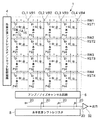
本発明の一実施の形態によるXYアドレス型固体撮像装置について図1乃至図5を用いて説明する。まず、本実施の形態によるXYアドレス型固体撮像装置としてのCMOSイメージセンサの概略構成を図1を用いて説明する。図1は、m行n列の画素配列を有するCMOSイメージセンサ1の4×4画素分の回路例を示している。複数の画素領域P11〜P44がマトリクス状に配列され、複数の垂直選択線CL1〜CL4と水平選択線RW1〜RW4とが縦横に配置されている。各画素領域P11〜P44には光電変換素子としてフォトダイオード10が形成されている。光電変換素子はフォトダイオード10に代えて例えばフォトゲートを用いてもよい。
【0019】
CMOSイメージセンサ1は、各画素領域P11〜P44に例えばMOSFET(本実施形態ではn−ch(nチャネル)MOSFETを例示している)で構成されるソースフォロワアンプ14や水平選択トランジスタ16等が配置されたAPS構成を有している。
以下、行番号をmとし、列番号をnとして画素領域Pmnの回路構成について説明する。画素領域Pmn内のフォトダイオード10のカソード側は、例えばn−chMOSFETのリセットトランジスタ12のソース電極及びソースフォロワアンプ14のゲート電極に接続されている。
【0020】
各リセットトランジスタ12のドレイン電極とソースフォロワアンプ14のドレイン電極は、リセット電圧VRが印加されるリセット電圧供給線VRnに接続されている。各リセットトランジスタ12のゲート電極はリセット信号線RSTmに接続されている。ソースフォロワアンプ14のソース電極は例えばn−chMOSFETの水平選択トランジスタ16のドレイン電極に接続されている。各水平選択トランジスタ16のゲート電極は水平選択信号RWが供給される水平選択線RWmに接続されている。各水平選択トランジスタ16のソース電極は垂直選択線CLnに接続されている。
【0021】
水平選択線RWmは、垂直走査シフトレジスタ/リセット制御回路4に接続されている。垂直走査シフトレジスタ/リセット制御回路4内に設けられた不図示のシフトレジスタにより、所定のタイミングで水平選択線RWmに順次水平選択信号RWが出力されるようになっている。リセット信号線RSTmも垂直走査シフトレジスタ/リセット制御回路4に接続され、所定のタイミングで水平選択線RWm毎に画素領域Pmnのリセットトランジスタ12にリセット信号RSTを印加するようになっている。
【0022】
リセット電圧供給線VRnは垂直選択線CLnにほぼ平行に配線され、垂直選択線CLnと共にそれぞれアンプ/ノイズキャンセル回路6に接続されている。垂直選択線CLnは、アンプ/ノイズキャンセル回路6内に設けられたCDS回路6CLnと、例えばn−chMOSFETで構成される列選択トランジスタ20とを介して信号共通出力線30に接続されている。アンプ/ノイズキャンセル回路6内のCDS回路6CLnの構成については図2を用いて後程説明する。リセット電圧供給線VRnは、アンプ/ノイズキャンセル回路6内に回路主要部が設けられたkTC雑音低減回路6VRnに接続されている。kTC雑音低減回路6VRnの構成については図3を用いて後程説明する。
【0023】
複数の列選択トランジスタ20のゲート電極には、水平走査シフトレジスタ8から列選択信号が所定タイミングで順次入力され、アンプ/ノイズキャンセル回路6により固定パターン雑音及びkTC雑音の除去された画像データが順次信号共通出力線30に出力され、アンプ32を介して外部システムに送出されるようになっている。
【0024】
次に、CMOSイメージセンサ1の動作について簡単に説明する。まず、リセット信号RSTによりリセットトランジスタ12が所定のタイミングでオンになると、フォトダイオード10がリセット電位VRに充電される。次いで光の入射に伴いフォトダイオード10の放電が始まり、リセット電位VRより電位が低下する。所定時間の経過後に水平選択信号RWが水平選択線RWmに出力されると当該水平選択線RWmに接続された水平選択トランジスタ16のゲート電極に水平選択信号RWが入力して水平選択トランジスタ16がオンになる。これによりソースフォロワアンプ14からの出力電圧が画素領域Pmnの画像データとして垂直選択線CLnに出力される。
【0025】
次に、アンプ/ノイズキャンセル回路6の構成について説明する。アンプ/ノイズキャンセル回路6は、図2に示すように、垂直選択線CL1に接続されたサンプルホールド回路及び相関二重サンプリング回路を有している。図2において、図中左側の破線で示したブロックは、垂直選択線CL1に接続された複数の画素のうち例示として図1左上の画素領域P11を示している。図中右側の破線で示したブロックは、サンプルホールド回路及び相関二重サンプリング回路を示している。
【0026】
サンプルホールド回路には垂直選択線CL1に出力された信号の入力を制御するサンプルホールド用スイッチ42が設けられている。サンプルホールド用スイッチ42の入力側と垂直選択線CL1との接続点には定電流源40が接続されている。サンプルホールド用スイッチ42の出力側には、垂直選択線CL1に出力された信号を保持するサンプルホールド用容量44の一電極側(これ以降、容量を構成する2つの電極及び、ゲート電極を除くトランジスタの2つの電極については、必要に応じて、一方を一電極、他方を他電極という)が接続されている。サンプルホールド用容量44の他電極側には基準電圧源46が接続されている。
【0027】
サンプルホールド用スイッチ42とサンプルホールド用容量44の一電極側との接続点には相関二重サンプリング回路を構成するアンプ48の入力端子が接続されている。アンプ48の出力端子は相関二重サンプリング回路のCDS用容量50の一電極側に接続され、CDS用容量50の他電極側はアンプ54の入力端子に接続されている。
【0028】
また、CDS用容量50の他電極側は、クランプスイッチ52を介してサンプルホールド用容量44の他電極側に接続されている。クランプスイッチ52の開閉によりCDS用容量50の他電極側を基準電圧源46の基準電圧から切り離し、あるいは基準電圧に固定することができるようになっている。アンプ54の出力端子は列選択トランジスタ20を介して信号共通出力線30に接続されている。
【0029】
次に、サンプルホールド回路及び相関二重サンプリング回路の動作について図2を用いて説明する。まず、画素領域P11から出力される信号の流れについて簡単に説明する。水平選択トランジスタ16のゲート電極に水平選択信号RW1が入力すると、画素領域P11のフォトダイオード10により蓄積された電荷量に応じたソースフォロワアンプ14の電圧変動が画像データを含む信号電圧VSとして垂直選択線CL1に出力される。次いで、水平選択トランジスタ16がオン状態を維持したままリセットトランジスタ12のゲート電極にリセット信号RSTを入力してリセットトランジスタ12をオン状態にさせ、フォトダイオード10をリセット電位VRにリセットすると共にリセット電圧VRを垂直選択線CL1に出力する。以上の動作は、水平ブランキング期間に行われる。
【0030】
上記の信号の流れにおいて、例えば、水平選択信号RW1が入力されて水平選択トランジスタ16がオン状態になるのに同期して、サンプルホールド用スイッチ42及びクランプスイッチ52がオン状態になる。これにより、サンプルホールド回路の入力端子に信号電圧VSが印加される。クランプスイッチ52がオン状態なので信号電圧VSはサンプルホールド回路のサンプルホールド用容量44を充電すると共にCDS用容量50も充電する。
【0031】
次いで、クランプスイッチ52をオフにしてから、リセット信号RSTを入力してリセットトランジスタ12をオン状態にする。これにより、フォトダイオード10はリセット電位VRにリセットされ、垂直選択線CL1にはリセット電圧VRが出力される。リセット電圧VRはサンプルホールド回路の入力端子に入力されてサンプルホールド用容量44に保持される。
【0032】
この結果、CDS用容量50の出力側には信号電圧VSとリセット電圧VRの差に相当する差信号(VS−VR)が生じる。この信号はCDS用容量50により保持される。こうすることにより、信号電圧VS及びリセット電圧VRの双方に重畳している固定パターン雑音成分を除去したアナログ画像データを得ることができる。このアナログ画像データは、アンプ54の出力端子から列選択トランジスタ20を介して信号共通出力線30に出力される。
【0033】
アンプ/ノイズキャンセル回路6内には上記サンプルホールド回路及び相関二重サンプリング回路(以下、両回路を合わせてCDS回路という)6CLnが垂直選択線CLnにそれぞれ設けられている。
【0034】
さらに本実施の形態によるアンプ/ノイズキャンセル回路6には、CDS回路6CLn毎に設けられ、CDS回路6CLnと協働してkTC雑音を低減させるkTC雑音低減回路が設けられている。
【0035】
以下、図3を用いて本実施の形態によるkTC雑音低減回路6VRnについて説明する。kTC雑音低減回路6VRnは、回路構成の大部分がアンプ/ノイズキャンセル回路6内に形成されると共に、回路構成の一部が画素領域Pmn内の素子を兼用している点に特徴を有している。図3において、図中左側の破線で示したブロックは、垂直選択線CL1に接続された画素領域P11を例示している。図中右側の破線で示したブロックは、アンプ/ノイズキャンセル回路6内のCDS回路6CL1及びkTC雑音低減回路6VR1の主要部を示している。なお、図3での相関二重サンプリング回路は詳細な記載を省略して1つの回路ブロックとして示している。
【0036】
図3において、アンプ/ノイズキャンセル回路6内に、画素領域P11内に形成された水平選択トランジスタ16とほぼ同一特性を有する回路切替用トランジスタ72が設けられ、そのソース電極は垂直選択線CL1に接続されている。回路切替用トランジスタ72のゲート電極には、回路切替信号SWXが入力するようになっている。回路切替信号SWXは、リセット信号RSTに同期して出力されるようになっている。
【0037】
回路切替用トランジスタ72のドレイン電極は、ソースフォロワアンプ14とほぼ同一特性を有する第1差動トランジスタ62のソース電極に接続されている。第1差動トランジスタ62のドレイン電極は、例えばMOS型のトランジスタ64の一電極側に接続され、トランジスタ64の他電極側には電圧VDDが印加されるようになっている。第1差動トランジスタ62のゲート電極には、リセット電圧VRが入力されるようになっている。
【0038】
一方、画素領域P11内のリセットトランジスタ12及びソースフォロワアンプ14のドレイン電極は、リセット電圧VRが印加されるリセット電圧供給線VR1を介して例えばMOS型のトランジスタ66の一電極側に接続されている。トランジスタ66の他電極側には電圧VDDが印加されるようになっている。リセット電圧供給線VR1は、複数の画素領域P11、P21、P31、・・・の外で垂直選択線CL1に沿って形成され、画素領域P11、P21、P31、・・・毎に形成された複数のリセットトランジスタ12にリセット電圧VRを供給するようになっている。
【0039】
トランジスタ66のゲート電極とトランジスタ64のゲート電極とは共通接続されている。また、第1差動トランジスタ62とトランジスタ64との接続点に一電極側が接続され、他電極側がトランジスタ64及びトランジスタ66のゲート電極に接続された回路切替用トランジスタ68が形成されている。回路切替用トランジスタ68のゲート電極には、回路切替信号SWXが入力するようになっている。また、トランジスタ64及びトランジスタ66のゲート電極に一電極側が接続され、他電極側が接地された回路切替用トランジスタ70が形成されている。回路切替用トランジスタ70のゲート電極には、回路切替信号SWXと逆極性の回路切替信号/SWXが入力するようになっている。
【0040】
ここで、画素領域P11の水平選択トランジスタ16及びアンプ/ノイズキャンセル回路6内の回路切替用トランジスタ68、72をオンにし、回路切替用トランジスタ70をオフにして、画素領域P11のソースフォロワアンプ14を第1差動トランジスタ62との差動対をなす第2差動トランジスタと見ることにより、図3の上記構成は、付加抵抗の代わりにカレントミラー回路を備えた差動増幅器となる。カレントミラー回路は、一電極側とゲート電極が直結されたp−chMOSFETのトランジスタ64と、トランジスタ64の他電極側と共に電圧VDDが印加される他電極側を備えトランジスタ64のゲート電極と共通接続されたゲート電極を有するp−chMOSFETのトランジスタ66とで構成される。
【0041】
以上、図3を用いて説明した回路が本実施の形態によるkTC雑音低減回路6VR1の回路構成であり、図示は省略したが他のkTC雑音低減回路6VRnも同様の構成を有している。このように、kTC雑音低減回路6VRnは回路構成の大部分がアンプ/ノイズキャンセル回路6内に形成されると共に、回路構成の一部を画素領域Pmn内の素子で兼用している。
【0042】
次に、図3に示すkTC雑音低減回路6VR1を例にとって、kTC雑音を低減させる動作について説明する。まず、リセット期間の終了直前までは、水平選択トランジスタ16及び回路切替用トランジスタ68、72はオン状態になっており、回路切替用トランジスタ70はオフ状態になっている。従って、kTC雑音低減回路6VR1の主要部が画素領域P11内の素子と電気的に接続され、kTC雑音低減回路6VR1は差動増幅器として機能してkTC雑音低減動作をしている状態になっている。
【0043】
リセット信号RSTが非活性レベルになると、水平選択トランジスタ16及び回路切替用トランジスタ68、72はオフ状態になり回路切替用トランジスタ70はオン状態になる。これにより、kTC雑音低減回路6VR1の主要部が画素領域P11内の素子と電気的に分離され、kTC雑音低減回路6VR1は差動増幅器として機能しなくなりkTC雑音低減動作をしない状態となる。一方、画素領域P11内の各素子は本来の信号蓄積動作を行う。
【0044】
次いで、所定時間の経過後に水平選択信号RW1が入力されて水平選択トランジスタ16がオン状態になるのに同期して、CDS回路6CL1のサンプルホールド用スイッチ42及びクランプスイッチ52が閉じて、垂直選択線CL1に出力された画素領域P11のソースフォロワアンプ14からの信号電圧VSがサンプルホールド用容量44及びCDS用容量50に充電される。
【0045】
次いで、クランプスイッチ52をオフにすると共に回路切替用トランジスタ70をオフ状態にして、回路切替用トランジスタ68、72をオン状態にする。これにより、kTC雑音低減回路6VR1は再び差動増幅器として機能してkTC雑音低減の動作状態となる。この状態で、画素領域P11のリセットトランジスタ12のゲート電極にリセット信号RSTが印加されるのに同期して第1差動トランジスタ62のゲート電極にリセット電圧VRを供給する。
【0046】
これにより、リセットトランジスタ12がオン状態の間、フォトダイオード10のカソード側の電位が常にリセット電圧VRになるように、kTC雑音低減回路6VR1のカレントミラー回路の出力側トランジスタ66の出力電圧(=リセット電圧VR)が制御される。このように、kTC雑音低減回路6VR1はリセット動作時に増幅率が1のオペアンプとして機能する。
【0047】
このようにすれば、フォトダイオード10をリセットする毎に生じるkTC雑音をほぼ一定にして、信号蓄積前のkTC雑音を含む信号電圧VSと信号蓄積後のリセット電圧VRに重畳するkTC雑音同士に相関関係を生じさせることができる。kTC雑音低減回路6VR1を用いてフォトダイオード10をリセット電位VRにリセットすると、垂直選択線CL1にはリセット電圧VRが出力される。リセット電圧VRはサンプルホールド回路の入力端子に入力されてサンプルホールド用容量44に保持される。
【0048】
この結果、CDS回路6CL1のCDS用容量50の出力側には信号電圧VSとリセット電圧VRの差に相当する差信号(VS−VR)が生じる。この信号はCDS用容量50により保持される。こうすることにより、信号電圧VS及びリセット電圧VRの双方に重畳している固定パターン雑音成分だけでなくkTC雑音も除去したアナログ画像データを得ることができる。このアナログ画像データは、アンプ54の出力端子から列選択トランジスタ20を介して信号共通出力線30に出力される。
【0049】
本実施の形態のkTC雑音低減回路6VRnによれば、回路主要部が画素領域外に配置され、また、kTC雑音低減動作時に、画素領域内の素子を回路構成の一部として用いて回路を構成するようになっているので、画素の開口率を低下させずにkTC雑音を低減することができる。
【0050】
なお、差動対をなす第1差動トランジスタ62とソースフォロワアンプ14の大きさ等を揃えてほぼ同特性にしても、両者間の配線距離に応じて変化するオフセット電圧が生じてしまう場合がある。しかもソースフォロワアンプ14のトランジスタが小さいためオフセット電圧は数十mVになる。これではフォトダイオード10のカソード側に印加されるリセット電圧VRが複数の画素領域毎にばらついてしまうので好ましくない。ある程度小さいオフセット電圧であれば、後段に配置されたCDS回路6CLnで除去することが可能だが、確実に除去するには図4の破線で囲んだオフセット補正回路を挿入することが望ましい。
【0051】
図4は、オフセット補正回路80の概略を示している。オフセット補正回路80の主要部はアンプ/ノイズキャンセル回路6内に設けられている。オフセット補正回路80は、第1差動トランジスタ62のゲート電極に印加するリセット電圧VRの入力段に挿入されたオフセット補正用トランジスタ82を有している。オフセット補正用トランジスタ82の一電極側は第1差動トランジスタ62のゲート電極に接続されている。またオフセット補正回路80は、kTC雑音低減回路6VR1が差動増幅器として機能した際に、制御されたリセット電圧VRが出力されるリセット電圧供給線VR1に一電極側が接続されたオフセット補正用トランジスタ86を有している。オフセット補正用トランジスタ86の他電極側には、オフセット補正用トランジスタ84及びオフセット補正用容量88の一電極側が接続されている。オフセット補正用トランジスタ84の他電極側はオフセット補正用トランジスタ82の他電極側に接続され、オフセット補正用容量88の他電極側はオフセット補正用トランジスタ82の一電極側(つまり、第1差動トランジスタ62のゲート電極)に接続されている。
【0052】
以上の構成のオフセット補正回路80によるオフセット電圧除去動作について説明する。まず、リセット信号RSTがリセットトランジスタ12のゲート電極に印加されるのに同期して、回路切替用トランジスタ68、70、72が動作して、kTC雑音低減回路6VR1が差動増幅器として機能するようになる。このリセット期間の初期において、オフセット補正用トランジスタ82、86はオン状態になり、オフセット補正用トランジスタ84はオフ状態になっている。このため、第1差動トランジスタ62のゲート電極にはリセット電圧VRが印加され、差動増幅器を介してリセット電圧供給線VR1にはオフセット電圧VOを含む電圧値VR+VOが出力される。従って、オフセット補正用容量88にはオフセット電圧VOが保持される。
【0053】
次いで、オフセット補正用トランジスタ82、86がオフになりオフセット補正用トランジスタ84がオンになると、第1差動トランジスタ62のゲート電極には電圧値VR−VOがリセット電圧として印加される。これにより、差動増幅器を介してリセット電圧供給線VR1に所望のリセット電圧VRが出力されるようになる。本動作はリセット期間の初期の段階で行われる。こうすることにより、各画素領域Pmn毎にばらつきのないリセット電圧VRを供給することができるようになる。
【0054】
図5は、本実施の形態のXYアドレス型固体撮像装置によるkTC雑音低減効果を比較例と共に示したシミュレーション図である。図において横軸は時間を表し、縦軸は電圧値を表している。図中破線αが本実施の形態のXYアドレス型固体撮像装置による効果を示す曲線であり、実線βは従来のXYアドレス型固体撮像装置を示す曲線である。図5は、時刻120nsecにリセット信号RSTがリセットトランジスタに入力して、フォトダイオードのカソード側の電位が約1.9Vになってから約200nsec後に10mVのDC成分のkTC雑音が重畳した場合におけるCDS回路からの出力電圧値を示している。図示のように、従来のXYアドレス型固体撮像装置では、CDS回路でkTC雑音を低減することができず、重畳したkTC雑音レベルとほぼ同一レベルの約10mVの雑音成分が現われている。それに対して、本実施の形態によるXYアドレス型固体撮像装置では、CDS回路からの出力電圧値の変動はわずかに0.25mV程度でありきわめて優れたkTC雑音低減効果を得ることができている。
【0055】
以上説明した実施の形態によるXYアドレス型固体撮像装置は、以下のようにまとめられる。
(付記1)
入射光を光電変換する光電変換素子と、前記光電変換素子をリセットするリセットトランジスタと、前記光電変換素子に蓄積された電荷を電圧に変換する増幅用トランジスタと、水平選択線に出力された水平選択信号に基づいて前記電圧を画像データとして垂直選択線に出力する水平選択トランジスタとを備えた画素領域と、
前記リセット時に発生するkTC雑音を低減させるkTC雑音低減回路と
を有することを特徴とするXYアドレス型固体撮像装置。
【0056】
(付記2)
付記1記載のXYアドレス型固体撮像装置において、
前記kTC雑音低減回路は、kTC雑音低減動作時に、前記画素領域内の素子を回路構成の一部として用いること
を特徴とするXYアドレス型固体撮像装置。
【0057】
(付記3)
付記2記載のXYアドレス型固体撮像装置において、
前記kTC雑音低減回路は、前記動作時に前記画素領域内の素子と電気的に接続し、非動作時に前記画素領域内の素子と電気的に分離する回路切替用トランジスタを有していること
を特徴とするXYアドレス型固体撮像装置。
【0058】
(付記4)
付記1乃至3のいずれか1項に記載のXYアドレス型固体撮像装置において、
前記画素領域外で前記垂直選択線に沿って形成され、前記リセットトランジスタにリセット電圧を供給するリセット電圧供給線を有していること
を特徴とするXYアドレス型固体撮像装置。
【0059】
(付記5)
付記3又は4に記載のXYアドレス型固体撮像装置において、
前記kTC雑音低減回路は、前記動作時に差動増幅器を構成する第1差動トランジスタを有し、
前記画素領域内の前記増幅用トランジスタは、前記kTC雑音低減回路の動作時に、前記第1差動トランジスタと対をなす第2差動トランジスタとして用いられること
を特徴とするXYアドレス型固体撮像装置。
【0060】
(付記6)
付記5記載のXYアドレス型固体撮像装置において、
前記回路切替用トランジスタは、前記第1差動トランジスタと前記垂直選択線との間に設けられていること
を特徴とするXYアドレス型固体撮像装置。
【0061】
(付記7)
付記5又は6に記載のXYアドレス型固体撮像装置において、
前記kTC雑音低減回路は、前記差動増幅器内にカレントミラー回路を備えていること
を特徴とするXYアドレス型固体撮像装置。
【0062】
(付記8)
付記7記載のXYアドレス型固体撮像装置において、
前記カレントミラー回路は、前記リセット電圧供給線に接続されていること
を特徴とするXYアドレス型固体撮像装置。
【0063】
(付記9)
付記1乃至8のいずれか1項に記載のXYアドレス型固体撮像装置において、
前記画像データに重畳する固定パターン雑音を除去するノイズキャンセル回路をさらに有し、
前記kTC雑音低減回路のうち、前記画素領域内の素子を除く回路は、前記ノイズキャンセル回路内に配置されていること
を特徴とするXYアドレス型固体撮像装置。
【0064】
(付記10)
付記9記載のXYアドレス型固体撮像装置において、
前記ノイズキャンセル回路は、雑音除去後の前記画像データに対応する電荷を保持する相関二重サンプリング回路を前記垂直選択線毎に有していること
を特徴とするXYアドレス型固体撮像装置。
【0065】
(付記11)
付記5乃至10のいずれか1項に記載のXYアドレス型固体撮像装置において、
前記増幅用トランジスタと前記第1差動トランジスタとの間の配線距離に応じて変化するオフセット電圧を補正するオフセット補正用回路をさらに有していること
を特徴とするXYアドレス型固体撮像装置。
【0066】
【発明の効果】
以上の通り、本発明によれば、小さな素子サイズで広い開口率を有し、kTC雑音を低減できるXYアドレス型固体撮像装置を実現できる。
【図面の簡単な説明】
【図1】本発明の一実施の形態によるCMOSイメージセンサ1の4×4画素分の回路例を示す図である。
【図2】本発明の一実施の形態によるCMOSイメージセンサ1のサンプルホールド回路及び相関二重サンプリング回路の回路例を示す図である。
【図3】本発明の一実施の形態によるCMOSイメージセンサ1のkTC雑音低減回路の回路例を示す図である。
【図4】本発明の一実施の形態によるCMOSイメージセンサ1のオフセット電圧補正回路の回路例を示す図である。
【図5】本発明の一実施の形態によるCMOSイメージセンサ1の効果を示す図である。
【図6】CMOSイメージセンサを用いた従来のXYアドレス型固体撮像装置を示す図である。
【図7】CMOSイメージセンサを用いた従来のXYアドレス型固体撮像装置の他の例を示す図である。
【図8】CMOSイメージセンサを用いた従来のXYアドレス型固体撮像装置のさらに他の例を示す図である。
【符号の説明】
1 CMOSイメージセンサ
4 垂直走査シフトレジスタ/リセット制御回路
6 アンプ/ノイズキャンセル回路
6CL1〜6CL4、6CLn CDS回路
6VR1〜6VR4、6VRn kTC雑音低減回路
8 水平走査シフトレジスタ
10、400 フォトダイオード
12、402 リセットトランジスタ
14、404 ソースフォロワアンプ
16、406 水平選択トランジスタ
20 列選択トランジスタ
30 信号共通出力線
48、54、412 アンプ
40、414 定電流電源
42 サンプルホールド用スイッチ
44 サンプルホールド用容量
46 基準電圧源
50 CDS用容量
52 クランプスイッチ
62 第1差動トランジスタ
64、66 トランジスタ(カレントミラー回路用)
68、70、72 回路切替用トランジスタ
80 オフセット補正回路
82、84、86 オフセット補正用トランジスタ
88 オフセット補正用容量
CL1〜CL4、CLn 垂直選択線
P11〜P44、Pmn 画素領域
RST リセット信号
RST1〜RST4、RSTm リセット信号線
RW1〜RW4、RWn 水平選択線
VR リセット電圧
VR1〜VR4、VRn リセット電圧供給線[0001]
BACKGROUND OF THE INVENTION
The present invention relates to a solid-state imaging device composed of semiconductor elements, and more particularly to an XY address type solid-state imaging device manufactured by a CMOS process.
[0002]
[Prior art]
2. Description of the Related Art In recent years, solid-state imaging devices have been used in large quantities by being incorporated in various products such as digital still cameras, digital video cameras, and mobile phones. Solid-state image pickup devices are roughly classified into CCD (Charge Coupled Device) solid-state image pickup devices constituted by charge transfer type image sensors, and XY address type solid-state image pickup devices constituted of image sensors by CMOS (complementary metal oxide semiconductor) transistors, for example. There is. An XY address type solid-state imaging device using a CMOS image sensor (hereinafter abbreviated as a CMOS image sensor as appropriate) can be manufactured by the same technology as the MOSFET manufacturing process, and is driven by a single power source to consume power. In addition, since various signal processing circuits can be mounted on the same chip, it is considered promising as an alternative to a CCD solid-state imaging device.
[0003]
A conventional XY address type solid-state imaging device using this CMOS image sensor will be described with reference to FIG. FIG. 6 shows a circuit example of one pixel of a conventional XY address type image sensor. The conventional CMOS image sensor shown in FIG. 6 has an APS (Active Pixel Sensor) configuration in which, for example, a
[0004]
The operation of this conventional CMOS image sensor will be briefly described. First, the reset signal RST is applied to the gate electrode of the
[0005]
However, in the conventional APS configuration in which the charge
[0006]
However, this method samples the reset voltage after signal accumulation instead of the reset voltage before signal accumulation (integration) to obtain a difference from the signal voltage, so that kTC noise (thermal noise) superimposed on the signal voltage is obtained. ) And the kTC noise superimposed on the sampled reset voltage. For this reason, the kTC noise generated randomly from the
[0007]
The kTC noise is generated when the
[0008]
Next, a CMOS image sensor capable of reducing kTC noise will be described with reference to FIG. In FIG. 7, a transfer gate FT that forms an energy barrier is provided between the first capacitance C1 of the
[0009]
When the charge is accumulated in the first capacitance C1 and then the transfer gate FT is turned on to transfer the charge to the second capacitance C2 in the FD region, the potential of the gate of the
[0010]
According to this configuration, since the reset voltage before signal accumulation is sampled and then the signal voltage after reset can be sampled, the kTC noise superimposed on the reset voltage and the signal voltage has a high correlation. For this reason, the kTC noise of the signal voltage can be reduced by sampling the reset voltage and then sampling the signal voltage and obtaining the difference between the reset voltage and the signal voltage using the correlated double sampling circuit.
[0011]
However, although the configuration of the conventional CMOS image sensor shown in FIG. 7 can reduce FPN and kTC noise as described above, it has a problem that the device configuration becomes complicated. The pixel element configuration shown in FIG. 7 has an increased number of transistors compared to the pixel element configuration shown in FIG. 6, and the pixel portion becomes complicated, resulting in a decrease in the aperture ratio (fill factor) of the light receiving portion. Have the problem of
[0012]
Next, another example of a CMOS image sensor capable of reducing kTC noise will be described with reference to FIG. The CMOS image sensor shown in FIG. 8 has a control circuit that controls the reset voltage applied to the gate electrode of the
[0013]
A reference reset signal VR is input to the non-inverting input terminal of the
[0014]
When the signal Vg is input to the gate electrode of the
[0015]
[Problems to be solved by the invention]
As described above, the CMOS image sensor shown in FIG. 6 has a problem that kTC noise cannot be reduced. On the other hand, the CMOS image sensor shown in FIGS. 7 and 8 has a problem that the element size increases in exchange for the reduction of kTC noise, and a wide aperture ratio cannot be obtained.
[0016]
An object of the present invention is to provide an XY address type solid-state imaging device that has a small aperture size and a wide aperture ratio and can reduce kTC noise.
[0017]
[Means for Solving the Problems]
The above purpose isIn an image sensor in which a gate of a source follower transistor is connected to one end of a photoelectric conversion element, and the potential of one end of the photoelectric conversion element is read as image data through the source follower transistor, an inverting input terminal is provided when the photoelectric conversion element is reset Is a gate of the source follower transistor and a non-inverting input terminal is a gate of the first differential transistor to which a constant voltage is applied, and the output of the differential amplifier is fed back to the inverting input terminal An image sensor characterized in that one end of the photoelectric conversion element is held at the constant voltageAchieved by:
In the image sensor of the present invention, the output of the differential amplifier is fed back to the inverting input terminal via a reset transistor for resetting the photoelectric conversion element.
In the image sensor of the present invention, the photoelectric conversion element, the source follower transistor, and the reset transistor constitute a pixel, and a plurality of the pixels are arranged in a matrix.
In the image sensor of the present invention, outputs of a plurality of the pixels are commonly connected to one vertical selection line, and the image data of each pixel is read out through the vertical selection line.
The image sensor of the present invention is characterized in that the first differential transistor constituting the differential amplifier is provided for each vertical selection line.
In the image sensor of the present invention, the first differential transistor is connected to the vertical selection line via a circuit switching transistor that is turned on in synchronization with an on operation of the reset transistor.
In the image sensor of the present invention, the reset transistors of the plurality of pixels are commonly connected to one reset voltage supply line.
In the image sensor of the present invention, the differential amplifier includes a current mirror circuit, and the current mirror circuit is provided for each of the reset voltage supply lines and is commonly connected to the reset voltage supply line. Each of which is supplied with the output of the differential amplifier.
In the image sensor of the present invention, the vertical selection line and the reset voltage supply line are arranged in parallel in a pair.
[0018]
DETAILED DESCRIPTION OF THE INVENTION
An XY address type solid-state imaging device according to an embodiment of the present invention will be described with reference to FIGS. First, a schematic configuration of a CMOS image sensor as an XY address type solid-state imaging device according to the present embodiment will be described with reference to FIG. FIG. 1 shows a circuit example for 4 × 4 pixels of a CMOS image sensor 1 having a pixel arrangement of m rows and n columns. A plurality of pixel regions P11 to P44 are arranged in a matrix, and a plurality of vertical selection lines CL1 to CL4 and horizontal selection lines RW1 to RW4 are arranged vertically and horizontally. A
[0019]
In the CMOS image sensor 1, a
Hereinafter, the circuit configuration of the pixel region Pmn will be described with the row number as m and the column number as n. The cathode side of the
[0020]
The drain electrode of each
[0021]
The horizontal selection line RWm is connected to the vertical scanning shift register /
[0022]
The reset voltage supply line VRn is wired substantially parallel to the vertical selection line CLn, and is connected to the amplifier / noise cancel
[0023]
A column selection signal is sequentially input from the horizontal scanning shift register 8 to the gate electrodes of the plurality of
[0024]
Next, the operation of the CMOS image sensor 1 will be briefly described. First, when the
[0025]
Next, the configuration of the amplifier / noise cancel
[0026]
The sample hold circuit is provided with a
[0027]
An input terminal of an
[0028]
The other electrode side of the
[0029]
Next, operations of the sample hold circuit and the correlated double sampling circuit will be described with reference to FIG. First, the flow of signals output from the pixel region P11 will be briefly described. When the horizontal selection signal RW1 is input to the gate electrode of the
[0030]
In the above signal flow, for example, the
[0031]
Next, after the
[0032]
As a result, a difference signal (VS−VR) corresponding to the difference between the signal voltage VS and the reset voltage VR is generated on the output side of the
[0033]
In the amplifier / noise cancel
[0034]
Furthermore, the amplifier / noise cancel
[0035]
Hereinafter, the kTC noise reduction circuit 6VRn according to the present embodiment will be described with reference to FIG. The kTC noise reduction circuit 6VRn is characterized in that most of the circuit configuration is formed in the amplifier /
[0036]
In FIG. 3, a
[0037]
The drain electrode of the
[0038]
On the other hand, the drain electrodes of the
[0039]
The gate electrode of the
[0040]
Here, the
[0041]
The circuit described with reference to FIG. 3 is the circuit configuration of the kTC noise reduction circuit 6VR1 according to the present embodiment. Although not shown, the other kTC noise reduction circuits 6VRn have the same configuration. As described above, most of the circuit configuration of the kTC noise reduction circuit 6VRn is formed in the amplifier / noise cancel
[0042]
Next, taking the kTC noise reduction circuit 6VR1 shown in FIG. 3 as an example, the kTC noise is reduced.ActionWill be described. First, until just before the end of the reset period, the
[0043]
When the reset signal RST becomes an inactive level, the
[0044]
Next, in synchronization with the horizontal selection signal RW1 being input and the
[0045]
Next, the
[0046]
Thereby, while the
[0047]
In this way, the kTC noise generated each time the
[0048]
As a result, a difference signal (VS−VR) corresponding to the difference between the signal voltage VS and the reset voltage VR is generated on the output side of the
[0049]
According to the kTC noise reduction circuit 6VRn of the present embodiment, the circuit main part is arranged outside the pixel region, and the circuit is configured by using elements in the pixel region as part of the circuit configuration during the kTC noise reduction operation. Thus, kTC noise can be reduced without reducing the aperture ratio of the pixel.
[0050]
Note that even if the first
[0051]
FIG. 4 shows an outline of the offset
[0052]
The offset voltage removal operation by the offset
[0053]
Next, when the offset
[0054]
FIG. 5 is a simulation diagram showing the kTC noise reduction effect of the XY address type solid-state imaging device of this embodiment together with a comparative example. In the figure, the horizontal axis represents time, and the vertical axis represents voltage value. In the figure, a broken line α is a curve showing the effect of the XY address type solid-state imaging device of the present embodiment, and a solid line β is a curve showing a conventional XY address type solid-state imaging device. FIG. 5 shows the CDS in the case where the reset signal RST is inputted to the reset transistor at time 120 nsec, and the kTC noise of the DC component of 10 mV is superimposed about 200 nsec after the potential on the cathode side of the photodiode becomes about 1.9 V. The output voltage value from the circuit is shown. As shown in the figure, in the conventional XY address type solid-state imaging device, the kTC noise cannot be reduced by the CDS circuit, and a noise component of about 10 mV, which is almost the same level as the superimposed kTC noise level, appears. On the other hand, in the XY address type solid-state imaging device according to the present embodiment, the fluctuation of the output voltage value from the CDS circuit is only about 0.25 mV, and an extremely excellent kTC noise reduction effect can be obtained.
[0055]
The XY address type solid-state imaging device according to the embodiment described above can be summarized as follows.
(Appendix 1)
A photoelectric conversion element that photoelectrically converts incident light, a reset transistor that resets the photoelectric conversion element, an amplifying transistor that converts electric charge accumulated in the photoelectric conversion element into a voltage, and a horizontal selection output to a horizontal selection line A pixel region comprising a horizontal selection transistor for outputting the voltage as image data to a vertical selection line based on a signal;
A kTC noise reduction circuit for reducing kTC noise generated at the time of resetting;
An XY address type solid-state imaging device characterized by comprising:
[0056]
(Appendix 2)
In the XY address type solid-state imaging device according to attachment 1,
The kTC noise reduction circuit uses an element in the pixel region as a part of a circuit configuration during a kTC noise reduction operation.
An XY address type solid-state imaging device.
[0057]
(Appendix 3)
In the XY address type solid-state imaging device according to
The kTC noise reduction circuit includes a circuit switching transistor that is electrically connected to an element in the pixel region during the operation and is electrically separated from an element in the pixel region during a non-operation.
An XY address type solid-state imaging device.
[0058]
(Appendix 4)
In the XY address type solid-state imaging device according to any one of appendices 1 to 3,
A reset voltage supply line that is formed along the vertical selection line outside the pixel region and supplies a reset voltage to the reset transistor;
An XY address type solid-state imaging device.
[0059]
(Appendix 5)
In the XY address type solid-state imaging device according to
The kTC noise reduction circuit includes a first differential transistor that forms a differential amplifier during the operation,
The amplifying transistor in the pixel region is used as a second differential transistor that forms a pair with the first differential transistor when the kTC noise reduction circuit operates.
An XY address type solid-state imaging device.
[0060]
(Appendix 6)
In the XY address type solid-state imaging device according to appendix 5,
The circuit switching transistor is provided between the first differential transistor and the vertical selection line.
An XY address type solid-state imaging device.
[0061]
(Appendix 7)
In the XY address type solid-state imaging device according to
The kTC noise reduction circuit includes a current mirror circuit in the differential amplifier.
An XY address type solid-state imaging device.
[0062]
(Appendix 8)
In the XY address type solid-state imaging device according to appendix 7,
The current mirror circuit is connected to the reset voltage supply line
An XY address type solid-state imaging device.
[0063]
(Appendix 9)
In the XY address type solid-state imaging device according to any one of appendices 1 to 8,
A noise cancellation circuit for removing fixed pattern noise superimposed on the image data;
Among the kTC noise reduction circuits, the circuits excluding the elements in the pixel region are arranged in the noise cancellation circuit.
An XY address type solid-state imaging device.
[0064]
(Appendix 10)
In the XY address type solid-state imaging device according to attachment 9,
The noise cancellation circuit has a correlated double sampling circuit for holding the charge corresponding to the image data after noise removal for each vertical selection line.
An XY address type solid-state imaging device.
[0065]
(Appendix 11)
In the XY address type solid-state imaging device according to any one of appendices 5 to 10,
An offset correction circuit for correcting an offset voltage that changes in accordance with a wiring distance between the amplifying transistor and the first differential transistor;
An XY address type solid-state imaging device.
[0066]
【The invention's effect】
As described above, according to the present invention, it is possible to realize an XY address type solid-state imaging device having a wide aperture ratio with a small element size and capable of reducing kTC noise.
[Brief description of the drawings]
FIG. 1 is a diagram showing a circuit example of 4 × 4 pixels of a CMOS image sensor 1 according to an embodiment of the present invention.
FIG. 2 is a diagram showing a circuit example of a sample hold circuit and a correlated double sampling circuit of the CMOS image sensor 1 according to one embodiment of the present invention.
FIG. 3 is a diagram showing a circuit example of a kTC noise reduction circuit of the CMOS image sensor 1 according to the embodiment of the present invention.
FIG. 4 is a diagram showing a circuit example of an offset voltage correction circuit of the CMOS image sensor 1 according to the embodiment of the present invention.
FIG. 5 is a diagram showing an effect of the CMOS image sensor 1 according to the embodiment of the present invention.
FIG. 6 is a diagram showing a conventional XY address type solid-state imaging device using a CMOS image sensor.
FIG. 7 is a diagram showing another example of a conventional XY address type solid-state imaging device using a CMOS image sensor.
FIG. 8 is a diagram showing still another example of a conventional XY address type solid-state imaging device using a CMOS image sensor.
[Explanation of symbols]
1 CMOS image sensor
4. Vertical scan shift register / reset control circuit
6 Amplifier / Noise cancellation circuit
6CL1-6CL4, 6CLn CDS circuit
6VR1-6VR4, 6VRn kTC noise reduction circuit
8 Horizontal scan shift register
10,400 photodiode
12, 402 Reset transistor
14,404 Source follower amplifier
16, 406 Horizontal selection transistor
20 column select transistor
30 Signal common output line
48, 54, 412 amplifier
40, 414 constant current power supply
42 Sample hold switch
44 Sample hold capacity
46 Reference voltage source
50 CDS capacity
52 Clamp switch
62 First differential transistor
64, 66 transistors (for current mirror circuit)
68, 70, 72 Circuit switching transistor
80 Offset correction circuit
82, 84, 86 Offset correction transistor
88 Offset correction capacity
CL1 to CL4, CLn vertical selection line
P11 to P44, Pmn pixel area
RST reset signal
RST1 to RST4, RSTm Reset signal line
RW1-RW4, RWn Horizontal selection line
VR reset voltage
VR1 to VR4, VRn reset voltage supply line
Claims (9)
該光電変換素子のリセット時に、反転入力端子が該ソースフォロワトランジスタのゲートであり、非反転入力端子が定電圧を印加された第1差動トランジスタのゲートである差動増幅器が構成され、該差動増幅器の出力を該反転入力端子に帰還することにより、該光電変換素子の一端を該定電圧に保持することを特徴とするイメージセンサ。In an image sensor in which a gate of a source follower transistor is connected to one end of a photoelectric conversion element, and the potential of one end of the photoelectric conversion element is read as image data through the source follower transistor.
When the photoelectric conversion element is reset, a differential amplifier is configured in which the inverting input terminal is the gate of the source follower transistor and the non-inverting input terminal is the gate of the first differential transistor to which a constant voltage is applied. An image sensor, wherein one end of the photoelectric conversion element is held at the constant voltage by feeding back an output of a dynamic amplifier to the inverting input terminal.
前記差動増幅器の出力が、前記光電変換素子をリセットするためのリセットトランジスタを介して前記反転入力端子に帰還されることを特徴とするイメージセンサ。The image sensor according to claim 1,
An image sensor, wherein an output of the differential amplifier is fed back to the inverting input terminal via a reset transistor for resetting the photoelectric conversion element.
前記光電変換素子、前記ソースフォロワトランジスタ、及び前記リセットトランジスタが画素を構成し、複数の該画素がマトリクス状に配置されていることを特徴とするイメージセンサ。The image sensor according to claim 2.
The image sensor, wherein the photoelectric conversion element, the source follower transistor, and the reset transistor constitute a pixel, and a plurality of the pixels are arranged in a matrix.
複数の前記画素の出力が一本の垂直選択線に共通接続され、各画素の前記画像データが該垂直選択線を介して読み出されることを特徴とするイメージセンサ。The image sensor according to claim 3,
An image sensor, wherein outputs of the plurality of pixels are commonly connected to one vertical selection line, and the image data of each pixel is read out through the vertical selection line.
前記差動増幅器を構成する前記第1差動トランジスタが、前記垂直選択線毎に設けられていることを特徴とするイメージセンサ。The image sensor according to claim 4.
An image sensor, wherein the first differential transistor constituting the differential amplifier is provided for each vertical selection line.
前記第1差動トランジスタは、前記リセットトランジスタのオン動作に同期してオンする回路切換用トランジスタを介して、前記垂直選択線に接続されることを特徴とするイメージセンサ。The image sensor according to claim 5,
The image sensor according to claim 1, wherein the first differential transistor is connected to the vertical selection line via a circuit switching transistor that is turned on in synchronization with an ON operation of the reset transistor.
前記複数の画素のリセットトランジスタが、一本のリセット電圧供給線に共通接続されていることを特徴とするイメージセンサ。The image sensor according to claim 6.
An image sensor, wherein the reset transistors of the plurality of pixels are commonly connected to one reset voltage supply line.
前記差動増幅器はカレントミラー回路を備え、該カレントミラー回路が、前記リセット電圧供給線毎に設けられ、該リセット電圧供給線に共通接続されている複数のリセットトランジスタのそれぞれに該差動増幅器の出力を供給することを特徴とするイメージセンサ。The image sensor according to claim 7,
The differential amplifier includes a current mirror circuit, and the current mirror circuit is provided for each reset voltage supply line, and each of the plurality of reset transistors commonly connected to the reset voltage supply line includes the current amplifier circuit. An image sensor characterized by supplying an output.
前記垂直選択線と前記リセット電圧供給線が、対をなして平行に配置されていることを特徴とするイメージセンサ。The image sensor according to claim 8.
The image sensor, wherein the vertical selection line and the reset voltage supply line are arranged in parallel in a pair.
Priority Applications (7)
| Application Number | Priority Date | Filing Date | Title |
|---|---|---|---|
| JP2001130148A JP3734717B2 (en) | 2001-04-26 | 2001-04-26 | Image sensor |
| TW090132226A TW541832B (en) | 2001-04-26 | 2001-12-25 | X-Y address type solid-state image pickup device |
| DE60105393T DE60105393T2 (en) | 2001-04-26 | 2001-12-27 | X-Y address solid-state imaging |
| EP01310898A EP1253781B1 (en) | 2001-04-26 | 2001-12-27 | X-Y address type solid-state image pickup device |
| US10/042,240 US6914631B2 (en) | 2001-04-26 | 2002-01-11 | Image sensor |
| KR1020020002666A KR100834424B1 (en) | 2001-04-26 | 2002-01-17 | Image sensor |
| CNB021027242A CN100429926C (en) | 2001-04-26 | 2002-01-24 | XY address type solid pick-up device |
Applications Claiming Priority (1)
| Application Number | Priority Date | Filing Date | Title |
|---|---|---|---|
| JP2001130148A JP3734717B2 (en) | 2001-04-26 | 2001-04-26 | Image sensor |
Publications (3)
| Publication Number | Publication Date |
|---|---|
| JP2002330348A JP2002330348A (en) | 2002-11-15 |
| JP2002330348A5 JP2002330348A5 (en) | 2004-10-07 |
| JP3734717B2 true JP3734717B2 (en) | 2006-01-11 |
Family
ID=18978574
Family Applications (1)
| Application Number | Title | Priority Date | Filing Date |
|---|---|---|---|
| JP2001130148A Expired - Fee Related JP3734717B2 (en) | 2001-04-26 | 2001-04-26 | Image sensor |
Country Status (7)
| Country | Link |
|---|---|
| US (1) | US6914631B2 (en) |
| EP (1) | EP1253781B1 (en) |
| JP (1) | JP3734717B2 (en) |
| KR (1) | KR100834424B1 (en) |
| CN (1) | CN100429926C (en) |
| DE (1) | DE60105393T2 (en) |
| TW (1) | TW541832B (en) |
Cited By (3)
| Publication number | Priority date | Publication date | Assignee | Title |
|---|---|---|---|---|
| US7864094B2 (en) | 2008-08-11 | 2011-01-04 | Sony Corporation | Solid-state image sensing device, imaging method, and imaging apparatus |
| US9041380B2 (en) | 2007-08-03 | 2015-05-26 | Sony Corporation | Reference voltage circuit and image-capture circuit |
| US11552212B2 (en) | 2020-05-11 | 2023-01-10 | Samsung Electronics Co., Ltd. | Sensors and electronic devices |
Families Citing this family (39)
| Publication number | Priority date | Publication date | Assignee | Title |
|---|---|---|---|---|
| JP2001189893A (en) * | 1999-12-28 | 2001-07-10 | Toshiba Corp | Solid-state image pickup device |
| JP3734717B2 (en) * | 2001-04-26 | 2006-01-11 | 富士通株式会社 | Image sensor |
| JP4132850B2 (en) | 2002-02-06 | 2008-08-13 | 富士通株式会社 | CMOS image sensor and control method thereof |
| KR100490598B1 (en) * | 2002-11-22 | 2005-05-17 | (주)하이칩스 | CMOS Image Sensor |
| US7317484B2 (en) * | 2003-02-26 | 2008-01-08 | Digital Imaging Systems Gmbh | CMOS APS readout scheme that combines reset drain current and the source follower output |
| US7280143B2 (en) * | 2003-04-14 | 2007-10-09 | Micron Technology, Inc. | CMOS image sensor with active reset and 4-transistor pixels |
| JP4207659B2 (en) * | 2003-05-16 | 2009-01-14 | ソニー株式会社 | Solid-state imaging device, driving method thereof, and camera device |
| US7626622B2 (en) * | 2004-01-13 | 2009-12-01 | Panasonic Corporation | Solid state image pickup device and camera using the same |
| KR100871688B1 (en) * | 2004-02-27 | 2008-12-08 | 삼성전자주식회사 | Solid State Imaging Device and Driving Method Therefor |
| TWI264086B (en) * | 2004-06-04 | 2006-10-11 | Via Tech Inc | Method and apparatus for image sensor |
| CN1981517B (en) * | 2004-07-06 | 2010-05-26 | 松下电器产业株式会社 | Solid-state imaging device |
| JP4481758B2 (en) * | 2004-07-28 | 2010-06-16 | 株式会社東芝 | Signal processing apparatus and data processing apparatus |
| US7294818B2 (en) * | 2004-08-24 | 2007-11-13 | Canon Kabushiki Kaisha | Solid state image pickup device and image pickup system comprising it |
| JP4878123B2 (en) * | 2005-02-07 | 2012-02-15 | 浜松ホトニクス株式会社 | Solid-state imaging device |
| KR100657863B1 (en) | 2005-02-07 | 2006-12-14 | 삼성전자주식회사 | Cmos active pixel sensor using fingered type source follower transistor |
| KR100691190B1 (en) * | 2005-07-13 | 2007-03-09 | 삼성전기주식회사 | Image Censor Array |
| JP5017895B2 (en) * | 2006-03-15 | 2012-09-05 | 日産自動車株式会社 | Infrared detector |
| JP4956084B2 (en) * | 2006-08-01 | 2012-06-20 | キヤノン株式会社 | Photoelectric conversion device and imaging system using the same |
| KR100879386B1 (en) | 2006-11-13 | 2009-01-20 | 삼성전자주식회사 | Cmos image senser and digital camera including thereof and image signal detecting method of cmos image senser |
| KR100849824B1 (en) * | 2007-03-09 | 2008-07-31 | 동부일렉트로닉스 주식회사 | Image sensor and method for manufacturing thereof |
| US7642498B2 (en) | 2007-04-04 | 2010-01-05 | Aptina Imaging Corporation | Capacitor multipler circuits and the applications thereof to attenuate row-wise temporal noise in image sensors |
| JP4311482B2 (en) | 2007-05-17 | 2009-08-12 | ソニー株式会社 | Imaging circuit, CMOS sensor, and imaging apparatus |
| US7999342B2 (en) * | 2007-09-24 | 2011-08-16 | Taiwan Semiconductor Manufacturing Company, Ltd | Image sensor element for backside-illuminated sensor |
| JP2009253559A (en) * | 2008-04-03 | 2009-10-29 | Sharp Corp | Solid-state imaging device and electronics information device |
| US20100252717A1 (en) * | 2008-09-29 | 2010-10-07 | Benoit Dupont | Active-pixel sensor |
| WO2010083527A2 (en) | 2009-01-16 | 2010-07-22 | Claret Medical, Inc. | Intravascular blood filter |
| KR101605831B1 (en) | 2009-08-24 | 2016-03-24 | 삼성전자주식회사 | Cmos image senser and image signal detecting method thereof |
| KR101898297B1 (en) * | 2010-03-08 | 2018-09-12 | 가부시키가이샤 한도오따이 에네루기 켄큐쇼 | Semiconductor device and driving method thereof |
| JP2013179479A (en) * | 2012-02-28 | 2013-09-09 | Nikon Corp | Solid-state imaging device and electronic camera using the same |
| CN104412574B (en) * | 2012-06-27 | 2017-12-12 | 松下知识产权经营株式会社 | Solid camera head |
| US9500752B2 (en) * | 2013-09-26 | 2016-11-22 | Varian Medical Systems, Inc. | Pixel architecture for imaging devices |
| JP6502597B2 (en) * | 2015-04-16 | 2019-04-17 | 株式会社半導体エネルギー研究所 | Imaging device |
| US9736413B1 (en) * | 2016-02-03 | 2017-08-15 | Sony Corporation | Image sensor and electronic device with active reset circuit, and method of operating the same |
| JP6632421B2 (en) * | 2016-02-22 | 2020-01-22 | キヤノン株式会社 | Solid-state imaging device and imaging device |
| CN107888807B (en) * | 2016-09-29 | 2020-07-24 | 普里露尼库斯股份有限公司 | Solid-state imaging device, method for driving solid-state imaging device, and electronic apparatus |
| CN111093043B (en) * | 2018-10-24 | 2021-10-22 | 宁波飞芯电子科技有限公司 | Radiation receiving system and method and sensing array |
| CN112840638B (en) | 2018-10-24 | 2024-03-15 | 宁波飞芯电子科技有限公司 | Reset method, reset device, reset system and pixel array using reset device |
| CN112345909B (en) * | 2019-08-07 | 2023-10-13 | 宁波飞芯电子科技有限公司 | Detection method, detection circuit and reset circuit |
| JP7336361B2 (en) | 2019-11-12 | 2023-08-31 | 株式会社ジャパンディスプレイ | detector |
Family Cites Families (16)
| Publication number | Priority date | Publication date | Assignee | Title |
|---|---|---|---|---|
| JP3008657B2 (en) * | 1992-03-04 | 2000-02-14 | ソニー株式会社 | Amplification type solid-state imaging device |
| US5369047A (en) * | 1993-07-01 | 1994-11-29 | Texas Instruments Incorporated | Method of making a BCD low noise high sensitivity charge detection amplifier for high performance image sensors |
| JP4035194B2 (en) * | 1996-03-13 | 2008-01-16 | キヤノン株式会社 | X-ray detection apparatus and X-ray detection system |
| US5892540A (en) * | 1996-06-13 | 1999-04-06 | Rockwell International Corporation | Low noise amplifier for passive pixel CMOS imager |
| JPH1198414A (en) * | 1997-09-16 | 1999-04-09 | Toshiba Corp | Amplifier circuit for mos solid-state image pickup element |
| US6493030B1 (en) * | 1998-04-08 | 2002-12-10 | Pictos Technologies, Inc. | Low-noise active pixel sensor for imaging arrays with global reset |
| US6697111B1 (en) * | 1998-04-08 | 2004-02-24 | Ess Technology, Inc. | Compact low-noise active pixel sensor with progressive row reset |
| JP4174106B2 (en) | 1998-08-31 | 2008-10-29 | キヤノン株式会社 | Photoelectric conversion device and imaging device using the same |
| US6128039A (en) * | 1999-01-11 | 2000-10-03 | Omnivision Technologies, Inc. | Column amplifier for high fixed pattern noise reduction |
| JP3601052B2 (en) * | 1999-03-11 | 2004-12-15 | 日本電気株式会社 | Solid-state imaging device |
| JP4154068B2 (en) * | 1999-04-12 | 2008-09-24 | キヤノン株式会社 | Solid-state imaging device, imaging system using the same, and image reading system |
| US6424375B1 (en) * | 1999-09-21 | 2002-07-23 | Pixel Devices, International | Low noise active reset readout for image sensors |
| WO2002027763A2 (en) * | 2000-09-25 | 2002-04-04 | Foveon, Inc. | Active pixel sensor with noise cancellation |
| US6339363B1 (en) * | 2000-12-04 | 2002-01-15 | Pixel Devices International | Low FPN high gain capacitive transimpedance amplifier for use with capacitive sensors |
| US6459078B1 (en) * | 2000-12-04 | 2002-10-01 | Pixel Devices International, Inc. | Image sensor utilizing a low FPN high gain capacitive transimpedance amplifier |
| JP3734717B2 (en) * | 2001-04-26 | 2006-01-11 | 富士通株式会社 | Image sensor |
-
2001
- 2001-04-26 JP JP2001130148A patent/JP3734717B2/en not_active Expired - Fee Related
- 2001-12-25 TW TW090132226A patent/TW541832B/en not_active IP Right Cessation
- 2001-12-27 EP EP01310898A patent/EP1253781B1/en not_active Expired - Lifetime
- 2001-12-27 DE DE60105393T patent/DE60105393T2/en not_active Expired - Lifetime
-
2002
- 2002-01-11 US US10/042,240 patent/US6914631B2/en not_active Expired - Lifetime
- 2002-01-17 KR KR1020020002666A patent/KR100834424B1/en not_active IP Right Cessation
- 2002-01-24 CN CNB021027242A patent/CN100429926C/en not_active Expired - Fee Related
Cited By (4)
| Publication number | Priority date | Publication date | Assignee | Title |
|---|---|---|---|---|
| US9041380B2 (en) | 2007-08-03 | 2015-05-26 | Sony Corporation | Reference voltage circuit and image-capture circuit |
| US7864094B2 (en) | 2008-08-11 | 2011-01-04 | Sony Corporation | Solid-state image sensing device, imaging method, and imaging apparatus |
| US11552212B2 (en) | 2020-05-11 | 2023-01-10 | Samsung Electronics Co., Ltd. | Sensors and electronic devices |
| US11855236B2 (en) | 2020-05-11 | 2023-12-26 | Samsung Electronics Co., Ltd. | Sensors and electronic devices |
Also Published As
| Publication number | Publication date |
|---|---|
| EP1253781B1 (en) | 2004-09-08 |
| TW541832B (en) | 2003-07-11 |
| JP2002330348A (en) | 2002-11-15 |
| DE60105393D1 (en) | 2004-10-14 |
| US6914631B2 (en) | 2005-07-05 |
| EP1253781A3 (en) | 2003-08-20 |
| KR100834424B1 (en) | 2008-06-04 |
| US20020158974A1 (en) | 2002-10-31 |
| KR20020083416A (en) | 2002-11-02 |
| EP1253781A2 (en) | 2002-10-30 |
| CN1383320A (en) | 2002-12-04 |
| DE60105393T2 (en) | 2005-02-17 |
| CN100429926C (en) | 2008-10-29 |
Similar Documents
| Publication | Publication Date | Title |
|---|---|---|
| JP3734717B2 (en) | Image sensor | |
| US8816266B2 (en) | Solid-state imaging device, method for driving solid-state imaging device, and electronic apparatus | |
| US6326230B1 (en) | High speed CMOS imager with motion artifact supression and anti-blooming | |
| US8743252B2 (en) | Solid-state imaging device for high density CMOS image sensor, and driving method thereof | |
| US9473720B2 (en) | Solid-state image-capturing device and image-capturing device | |
| CN111901540B (en) | Image pickup apparatus | |
| US20170244844A1 (en) | Solid-state image sensor and image reading apparatus | |
| US8159586B2 (en) | Solid-state imaging apparatus | |
| US10559614B2 (en) | Dual conversion gain circuitry with buried channels | |
| JP2009532938A (en) | Noise reduction in imagers | |
| JP2010141928A (en) | Solid-state image pickup device | |
| JP2008511255A (en) | Pixel reset voltage booster pixel | |
| US20050253946A1 (en) | Solid-state image pickup device and camera utilizing the same | |
| JP4533367B2 (en) | Solid-state imaging device | |
| CN112291493B (en) | Imaging system and method for generating high dynamic range images | |
| US7619671B2 (en) | Method, apparatus and system for charge injection suppression in active pixel sensors | |
| US9807329B2 (en) | Imaging device and imaging system | |
| JP4746962B2 (en) | Solid-state imaging device and imaging system | |
| JP6809526B2 (en) | Image sensor and image sensor | |
| US20230353898A1 (en) | Solid-state imaging device, method for driving solid-state imaging device, and electronic apparatus | |
| JP4640102B2 (en) | Omni-directional camera | |
| JP2007214791A (en) | Imaging element, imaging apparatus, and driving method of imaging element | |
| JP2006067453A (en) | Solid state imaging device, camera, and video camera | |
| JP2024009651A (en) | Photoelectric conversion device, imaging system, and apparatus | |
| JP2009171035A (en) | Solid-state imaging element |
Legal Events
| Date | Code | Title | Description |
|---|---|---|---|
| A977 | Report on retrieval |
Free format text: JAPANESE INTERMEDIATE CODE: A971007 Effective date: 20050726 |
|
| A131 | Notification of reasons for refusal |
Free format text: JAPANESE INTERMEDIATE CODE: A131 Effective date: 20050809 |
|
| A521 | Request for written amendment filed |
Free format text: JAPANESE INTERMEDIATE CODE: A523 Effective date: 20050829 |
|
| TRDD | Decision of grant or rejection written | ||
| A01 | Written decision to grant a patent or to grant a registration (utility model) |
Free format text: JAPANESE INTERMEDIATE CODE: A01 Effective date: 20051011 |
|
| A61 | First payment of annual fees (during grant procedure) |
Free format text: JAPANESE INTERMEDIATE CODE: A61 Effective date: 20051019 |
|
| R150 | Certificate of patent or registration of utility model |
Free format text: JAPANESE INTERMEDIATE CODE: R150 |
|
| S111 | Request for change of ownership or part of ownership |
Free format text: JAPANESE INTERMEDIATE CODE: R313111 |
|
| FPAY | Renewal fee payment (event date is renewal date of database) |
Free format text: PAYMENT UNTIL: 20081028 Year of fee payment: 3 |
|
| R371 | Transfer withdrawn |
Free format text: JAPANESE INTERMEDIATE CODE: R371 |
|
| S111 | Request for change of ownership or part of ownership |
Free format text: JAPANESE INTERMEDIATE CODE: R313111 |
|
| FPAY | Renewal fee payment (event date is renewal date of database) |
Free format text: PAYMENT UNTIL: 20081028 Year of fee payment: 3 |
|
| FPAY | Renewal fee payment (event date is renewal date of database) |
Free format text: PAYMENT UNTIL: 20091028 Year of fee payment: 4 |
|
| R350 | Written notification of registration of transfer |
Free format text: JAPANESE INTERMEDIATE CODE: R350 |
|
| FPAY | Renewal fee payment (event date is renewal date of database) |
Free format text: PAYMENT UNTIL: 20091028 Year of fee payment: 4 |
|
| FPAY | Renewal fee payment (event date is renewal date of database) |
Free format text: PAYMENT UNTIL: 20101028 Year of fee payment: 5 |
|
| FPAY | Renewal fee payment (event date is renewal date of database) |
Free format text: PAYMENT UNTIL: 20101028 Year of fee payment: 5 |
|
| FPAY | Renewal fee payment (event date is renewal date of database) |
Free format text: PAYMENT UNTIL: 20111028 Year of fee payment: 6 |
|
| FPAY | Renewal fee payment (event date is renewal date of database) |
Free format text: PAYMENT UNTIL: 20111028 Year of fee payment: 6 |
|
| S531 | Written request for registration of change of domicile |
Free format text: JAPANESE INTERMEDIATE CODE: R313531 |
|
| S533 | Written request for registration of change of name |
Free format text: JAPANESE INTERMEDIATE CODE: R313533 |
|
| FPAY | Renewal fee payment (event date is renewal date of database) |
Free format text: PAYMENT UNTIL: 20111028 Year of fee payment: 6 |
|
| R350 | Written notification of registration of transfer |
Free format text: JAPANESE INTERMEDIATE CODE: R350 |
|
| FPAY | Renewal fee payment (event date is renewal date of database) |
Free format text: PAYMENT UNTIL: 20111028 Year of fee payment: 6 |
|
| FPAY | Renewal fee payment (event date is renewal date of database) |
Free format text: PAYMENT UNTIL: 20121028 Year of fee payment: 7 |
|
| FPAY | Renewal fee payment (event date is renewal date of database) |
Free format text: PAYMENT UNTIL: 20121028 Year of fee payment: 7 |
|
| FPAY | Renewal fee payment (event date is renewal date of database) |
Free format text: PAYMENT UNTIL: 20131028 Year of fee payment: 8 |
|
| S111 | Request for change of ownership or part of ownership |
Free format text: JAPANESE INTERMEDIATE CODE: R313111 |
|
| R350 | Written notification of registration of transfer |
Free format text: JAPANESE INTERMEDIATE CODE: R350 |
|
| LAPS | Cancellation because of no payment of annual fees |