JP3703083B2 - Waveform generator - Google Patents
Waveform generator Download PDFInfo
- Publication number
- JP3703083B2 JP3703083B2 JP2001002676A JP2001002676A JP3703083B2 JP 3703083 B2 JP3703083 B2 JP 3703083B2 JP 2001002676 A JP2001002676 A JP 2001002676A JP 2001002676 A JP2001002676 A JP 2001002676A JP 3703083 B2 JP3703083 B2 JP 3703083B2
- Authority
- JP
- Japan
- Prior art keywords
- data
- waveform
- band
- signal
- address
- Prior art date
- Legal status (The legal status is an assumption and is not a legal conclusion. Google has not performed a legal analysis and makes no representation as to the accuracy of the status listed.)
- Expired - Fee Related
Links
Images


Classifications
-
- H—ELECTRICITY
- H03—ELECTRONIC CIRCUITRY
- H03D—DEMODULATION OR TRANSFERENCE OF MODULATION FROM ONE CARRIER TO ANOTHER
- H03D7/00—Transference of modulation from one carrier to another, e.g. frequency-changing
-
- G—PHYSICS
- G06—COMPUTING; CALCULATING OR COUNTING
- G06F—ELECTRIC DIGITAL DATA PROCESSING
- G06F1/00—Details not covered by groups G06F3/00 - G06F13/00 and G06F21/00
- G06F1/02—Digital function generators
- G06F1/03—Digital function generators working, at least partly, by table look-up
- G06F1/0321—Waveform generators, i.e. devices for generating periodical functions of time, e.g. direct digital synthesizers
-
- H—ELECTRICITY
- H03—ELECTRONIC CIRCUITRY
- H03H—IMPEDANCE NETWORKS, e.g. RESONANT CIRCUITS; RESONATORS
- H03H17/00—Networks using digital techniques
- H03H17/02—Frequency selective networks
- H03H17/06—Non-recursive filters
- H03H17/0607—Non-recursive filters comprising a ROM addressed by the input data signals
Description
【0001】
【発明の属する技術分野】
本発明は、移動体通信端末装置に設けられ、デジタル信号を変調するための変調装置において、複数の帯域制限特性に対応して動作可能な波形発生装置に関する。
【0002】
【従来の技術】
近年、通信や放送のデジタル化が進められているなかで、デジタル変調技術はより多くの情報を正確に伝送する上で必要不可欠な技術である。また、LSI(大規模集積回路)技術の進歩によって、これまで複数のチップで構成されていた機能・システムが、1チップに集積される傾向にある。このような背景の下、移動体通信分野においては、1台の端末装置で複数の通信方式に対応することが可能な共用端末装置が求められている。一般的に変調装置において必要不可欠な帯域制限フィルタの特性は各通信方式の規格で定められているが、それぞれ異なるため、共用端末装置には複数の帯域制限特性を有する波形発生装置を設ける必要がある。
【0003】
ところで、デジタル信号を帯域制限して伝送する場合、その帯域制限フィルタによって生じるデジタル信号間の干渉(符号間干渉)を防ぐために、ロールオフフィルタが使用される。ここで、帯域制限特性の異なる場合とは、遮断特性を決定するロールオフ率が異なる場合や、ナイキストフィルタとルートナイキストフィルタのように特性関数自体が異なる場合である。図2(a)は、ロールオフ率(α)が0.5と0.25のナイキストフィルタのインパルス応答波形(±3シンボル周期分)を示しており、図2(b)は、ロールオフ率がともに0.5のナイキストフィルタとルートナイキストフィルタのインパルス応答波形(±3シンボル周期分)を示している。同図から明らかなように、ロールオフフィルタには、共通してインパルス応答波形の中心振幅が1付近で、残りのシンボル点では、振幅が0付近となるという性質がある。この性質によって、入力信号系列に対する符号間干渉を抑えて情報を正確に伝送することが可能となる。図3(a)および(b)は、図2(a)および(b)に示された帯域制限特性で2値信号系列{−1,−1,−1,−1,+1,+1,+1}の計7シンボルをそれぞれ帯域制限した場合の各出力波形と出力波形間の振幅値の差分(差分信号)を示している。同図から明らかなように、いずれの帯域制限特性で帯域制限した場合の出力波形においても、各シンボル点において入力されたシンボル値の振幅値付近を通過している。その結果、帯域制限特性が多少異なっていても、差分信号は各出力波形の振幅値よりも遥かに小さいものである。
【0004】
上述したようなロールオフフィルタはデジタルフィルタで実現可能であるが、複数のデジタル乗算器を使用するため回路規模が大きくなる。従って、小さい回路規模で実現する手段としては、ROM(読み出し専用メモリ)を使用した構成が一般的である。
【0005】
ROMを用いたロールオフフィルタでは、帯域制限特性に応じたインパルス応答と入力信号系列とのたたみ込み演算を予め行い、その結果をROMに格納しておく。そして、入力信号系列に応じてROMからデータ(たたみ込み演算の結果)を読み出し、帯域制限された信号として出力する。帯域制限特性に応じた演算結果をROMに格納するため、複数の帯域制限特性を有するロールオフフィルタが必要な場合には、複数のROMを設ける必要がある。
【0006】
図9は、複数の帯域制限特性に対応して動作可能な従来の波形発生装置の一例を示すブロック図である。同図において、この波形発生装置には、第1の帯域制限特性を有する波形発生装置92と、第2の帯域制限特性を有する波形発生装置93とが設けられている。そして、第1の帯域制限特性が要求される場合には、入力端子91から入力された信号系列は切換えスイッチ94を介して波形発生装置92に供給され、この波形発生装置92からの出力が切換えスイッチ95および出力端子96を介して、第1の帯域制限特性で帯域制限された信号として出力されるようになっている。一方、第2の帯域制限特性が要求される場合には、切換えスイッチ94および95が切換えられる。そして、入力端子91から入力された信号系列は切換えスイッチ94を介して波形発生装置93に供給され、この波形発生装置93からの出力が切換えスイッチ95および出力端子96を介して、第2の帯域制限特性で帯域制限された信号として出力されるようになっている。
【0007】
図10は、図9に示した波形発生装置の具体的な構成例を示すブロック図である。なお、この構成例は、第1の帯域制限フィルタと第2の帯域制限フィルタとで、帯域制限特性、演算時のデータ補間率、演算結果のビット精度が異なる場合のものである。図10において、波形発生装置92は、カウンタ101aと、アドレス発生装置102aと、第1の帯域制限フィルタとしてのROM103aと、D/A(デジタル/アナログ)変換器104aと、ポストフィルタ105aとから構成されており、波形発生装置93は、カウンタ101bと、アドレス発生装置102bと、第2の帯域制限フィルタとしてのROM103bと、D/A変換器104bと、ポストフィルタ105bとから構成されている。
【0008】
次に、第1の帯域制限特性が要求される場合の動作について説明する。入力端子91から入力されたシンボル周期Tの信号系列はシフトレジスタ100に供給され、クロック信号CLK1(1/Tの周波数)に応じて順次シフトされる。アドレス発生装置102aには、このシフトレジスタ100からの出力が切換えスイッチ94を介して供給されるとともに、第1の帯域制限特性でのデータ補間率に対応したクロック信号CLK2(CLK1の自然数倍の周波数)をカウントするカウンタ101aからの出力が供給される。アドレス発生装置102aでは、シフトレジスタ100からの出力およびカウンタ101aからの出力に応じてアドレスデータが発生され、これがROM103aに供給される。ROM103aからは、供給されたアドレスデータに応じて、予め格納された波形データが読み出され、nビット(nは自然数)のデジタルデータとして出力される。従って、ROM103aには、(2のn乗)通りの波形データを格納しておく必要がある。分解能nビットのD/A変換器104aには、ROM103aからのデジタルデータが供給されるとともに、クロック信号CLK2が供給される。このD/A変換器104aでは、ROM103aから供給されたデジタルデータがクロック信号CLK2の周期でアナログ信号に変換され、このアナログ信号がポストフィルタ105aに供給される。ポストフィルタ105aでは、供給されたアナログ信号から折り返しノイズが除去され、その結果得られた信号が切換えスイッチ95および出力端子96を介して、第1の帯域制限特性で帯域制限された信号として出力されるようになっている。
【0009】
続いて、第2の帯域制限特性が要求される場合の動作について説明する。この場合には、切換えスイッチ94および95が切換えられる。そして、アドレス発生装置102bには、シフトレジスタ100からの出力が切換えスイッチ94を介して供給されるとともに、第2の帯域制限特性でのデータ補間率に対応したクロック信号CLK3(CLK1の自然数倍の周波数)をカウントするカウンタ101bからの出力が供給される。アドレス発生装置102bでは、シフトレジスタ100からの出力およびカウンタ101bからの出力に応じてアドレスデータが発生され、これがROM103bに供給される。ROM103bからは、供給されたアドレスデータに応じて、予め格納された波形データが読み出され、mビット(mは自然数)のデジタルデータとして出力される。従って、ROM103bには、(2のm乗)通りの波形データを格納しておく必要がある。分解能mビットのD/A変換器104bには、ROM103bからのデジタルデータが供給されるとともに、クロック信号CLK3が供給される。このD/A変換器104bでは、ROM103bから供給されたデジタルデータがクロック信号CLK3の周期でアナログ信号に変換され、このアナログ信号がポストフィルタ105bに供給される。ポストフィルタ105bでは、供給されたアナログ信号から折り返しノイズが除去され、その結果得られた信号が切換えスイッチ95および出力端子96を介して、第2の帯域制限特性で帯域制限された信号として出力されるようになっている。
【0010】
図11は、図9に示した波形発生装置の他の具体的な構成例を示すブロック図である。なお、この構成例は、第1の帯域制限フィルタと第2の帯域制限フィルタとで、演算時のデータ補間率、演算結果のビット精度は等しく、帯域制限特性のみが異なる場合のものである。図11において、波形発生装置92は、カウンタ101aと、アドレス発生装置102aと、第1の帯域制限フィルタとしてのROM103aと、D/A変換器104aと、ポストフィルタ105aとから構成されており、波形発生装置93は、カウンタ101aと、アドレス発生装置102aと、第2の帯域制限フィルタとしてのROM103bと、D/A変換器104aと、ポストフィルタ105aとから構成されている。すなわち、カウンタ101a、アドレス発生装置102a、D/A変換器104a、ポストフィルタ105aは、波形発生装置92および93に共通の構成要素となっている。
【0011】
次に、第1の帯域制限特性が要求される場合の動作について説明する。入力端子91から入力されたシンボル周期Tの信号系列はシフトレジスタ100に供給され、クロック信号CLK1(1/Tの周波数)に応じて順次シフトされる。アドレス発生装置102aには、このシフトレジスタ100からの出力が供給されるとともに、データ補間率に対応したクロック信号CLK2(CLK1の自然数倍の周波数)をカウントするカウンタ101aからの出力が供給される。アドレス発生装置102aでは、シフトレジスタ100からの出力およびカウンタ101aからの出力に応じてアドレスデータが発生され、これが切換えスイッチ94を介してROM103aに供給される。ROM103aからは、供給されたアドレスデータに応じて、予め格納された波形データが読み出され、nビット(nは自然数)のデジタルデータとして出力される。分解能nビットのD/A変換器104aには、ROM103aからのデジタルデータが切換えスイッチ95を介して供給されるとともに、クロック信号CLK2が供給される。このD/A変換器104aでは、ROM103aから供給されたデジタルデータがクロック信号CLK2の周期でアナログ信号に変換され、このアナログ信号がポストフィルタ105aに供給される。ポストフィルタ105aでは、供給されたアナログ信号から折り返しノイズが除去され、その結果得られた信号が出力端子96から、第1の帯域制限特性で帯域制限された信号として出力されるようになっている。
【0012】
続いて、第2の帯域制限特性が要求される場合の動作について説明する。この場合には、切換えスイッチ94および95が切換えられる。そして、アドレス発生装置102aからのアドレスデータが、切換えスイッチ94を介してROM103bに供給される。ROM103bからは、供給されたアドレスデータに応じて、予め格納された波形データが読み出され、nビットのデジタルデータとして出力される。D/A変換器104aには、ROM103bからのデジタルデータが切換えスイッチ95を介して供給されるとともに、クロック信号CLK2が供給される。このD/A変換器104aでは、ROM103bから供給されたデジタルデータがクロック信号CLK2の周期でアナログ信号に変換され、このアナログ信号がポストフィルタ105aに供給される。ポストフィルタ105aでは、供給されたアナログ信号から折り返しノイズが除去され、その結果得られた信号が出力端子96から、第2の帯域制限特性で帯域制限された信号として出力されるようになっている。
【0013】
【発明が解決しようとする課題】
上述したように、第1の帯域制限フィルタと第2の帯域制限フィルタとで、演算時のデータ補間率、演算結果のビット精度は等しく、帯域制限特性のみが異なる場合には、図11に示したような構成を採用することにより、図10に示したものより多少は回路規模を小さくすることができる。しかしながら、いずれにしても帯域制限フィルタは2個設けることが必要であり、これらのフィルタをROMで実現したとしても、あまり回路規模を小さくすることはできない。
【0014】
本発明は、このような従来の問題点に鑑みて為されたものであり、複数の帯域制限特性に対応して動作可能な、回路規模の小さい波形発生装置を提供することを目的としている。
【0015】
【課題を解決するための手段】
上述した目的を達成するため、第1に、本発明の波形発生装置は、複数の帯域制限特性に対応して動作可能な波形発生装置において、入力信号系列に応じて第1の帯域制限特性で帯域制限された波形信号を発生させる波形発生手段と、前記入力信号系列に対する第1の帯域制限特性で帯域制限された波形信号と、前記入力信号系列に対する第2の帯域制限特性で帯域制限された波形信号との差分信号が予め格納されており、前記入力信号系列に応じて前記差分信号を出力するメモリ手段と、前記波形発生手段からの波形信号と前記メモリ手段からの差分信号との加算処理を行い、第2の帯域制限特性で帯域制限された波形信号を出力する加算手段と、前記波形発生手段からの波形信号および前記加算手段からの波形信号のいずれか一方を選択的に出力する切換えスイッチ手段と、を備えてなることを特徴としている。
【0016】
第2に、本発明の波形発生装置は、複数の帯域制限特性に対応して動作可能な波形発生装置において、入力信号系列に応じてアドレスデータを発生させる第1のアドレス発生手段と、第1の帯域制限特性で帯域制限された結果を示す波形データが予め格納されており、前記第1のアドレス発生手段からのアドレスデータに応じて前記波形データを出力する第1のメモリ手段と、前記入力信号系列に応じてアドレスデータを発生させる第2のアドレス発生手段と、第1の帯域制限特性で帯域制限された結果を示す波形データと第2の帯域制限特性で帯域制限された結果を示す波形データとの差分データが予め格納されており、前記第2のアドレス発生手段からのアドレスデータに応じて前記差分データを出力する第2のメモリ手段と、前記第1のメモリ手段からの波形データと前記第2のメモリ手段からの差分データとの加算処理を行い、第2の帯域制限特性で帯域制限された結果を示す波形データを出力するデジタル加算手段と、前記第1のメモリ手段からの波形データおよび前記デジタル加算手段からの波形データのいずれか一方をアナログ信号に変換するデジタル/アナログ変換手段と、前記デジタル/アナログ変換手段からのアナログ信号から折り返しノイズを除去して出力するフィルタ手段と、を備えてなることを特徴としている。
【0017】
第3に、本発明の波形発生装置は、複数の帯域制限特性に対応して動作可能な波形発生装置において、入力信号系列に応じてアドレスデータを発生させる第1のアドレス発生手段と、第1の帯域制限特性で帯域制限された結果を示す波形データが予め格納されており、前記第1のアドレス発生手段からのアドレスデータに応じて前記波形データを出力する第1のメモリ手段と、前記第1のメモリ手段からの波形データをアナログ信号に変換する第1のデジタル/アナログ変換手段と、前記入力信号系列に応じてアドレスデータを発生させる第2のアドレス発生手段と、第1の帯域制限特性で帯域制限された結果を示す波形データと第2の帯域制限特性で帯域制限された結果を示す波形データとの差分データが予め格納されており、前記第2のアドレス発生手段からのアドレスデータに応じて前記差分データを出力する第2のメモリ手段と、前記第2のメモリ手段からの差分データをアナログ信号に変換する第2のデジタル/アナログ変換手段と、前記第1のデジタル/アナログ変換手段からの波形データに基づくアナログ信号と前記第2のデジタル/アナログ変換手段からの差分データに基づくアナログ信号との加算処理を行い、第2の帯域制限特性で帯域制限された結果を示す波形データに相当するアナログ信号を出力するアナログ加算手段と、前記第1のデジタル/アナログ変換手段からのアナログ信号および前記アナログ加算手段からのアナログ信号のいずれか一方から折り返しノイズを除去して出力するフィルタ手段と、を備えてなることを特徴としている。
【0018】
第4に、本発明の波形発生装置は、複数の帯域制限特性に対応して動作可能な波形発生装置において、入力信号系列に応じてアドレスデータを発生させる第1のアドレス発生手段と、第1の帯域制限特性で帯域制限された結果を示す波形データが第1のデータ補間率で予め格納されており、前記第1のアドレス発生手段からのアドレスデータに応じて前記波形データを出力する第1のメモリ手段と、前記第1のメモリ手段からの波形データを第1のデータ補間率に対応した第1のクロック信号の周期でアナログ信号に変換する第1のデジタル/アナログ変換手段と、前記入力信号系列に応じてアドレスデータを発生させる第2のアドレス発生手段と、第1の帯域制限特性で帯域制限された結果を示す波形データと第2の帯域制限特性で帯域制限された結果を示す波形データとの差分データが第2のデータ補間率で予め格納されており、前記第2のアドレス発生手段からのアドレスデータに応じて前記差分データを出力する第2のメモリ手段と、前記第2のメモリ手段からの差分データを第2のデータ補間率に対応した第2のクロック信号の周期でアナログ信号に変換する第2のデジタル/アナログ変換手段と、前記第1のデジタル/アナログ変換手段からの波形データに基づくアナログ信号と前記第2のデジタル/アナログ変換手段からの差分データに基づくアナログ信号との加算処理を行い、第2の帯域制限特性で帯域制限された結果を示す波形データに相当するアナログ信号を出力するアナログ加算手段と、前記第1のデジタル/アナログ変換手段からのアナログ信号から折り返しノイズを除去する第1のフィルタ手段と、前記アナログ加算手段からのアナログ信号から折り返しノイズを除去する第2のフィルタ手段と、前記第1のフィルタ手段からの信号および前記第2のフィルタ手段からの信号のいずれか一方を選択的に出力する切換えスイッチ手段と、を備えてなることを特徴としている。
【0019】
第5に、本発明の波形発生装置は、複数の帯域制限特性に対応して動作可能な波形発生装置において、入力信号系列に応じてアドレスデータを発生させる第1のアドレス発生手段と、第1の帯域制限特性で帯域制限された結果を示す波形データが第1のデータ補間率で予め格納されており、前記第1のアドレス発生手段からのアドレスデータに応じて前記波形データを出力する第1のメモリ手段と、前記入力信号系列に応じてアドレスデータを発生させる第2のアドレス発生手段と、第1の帯域制限特性で帯域制限された結果を示す波形データと第2の帯域制限特性で帯域制限された結果を示す波形データとの差分データが第2のデータ補間率で予め格納されており、前記第2のアドレス発生手段からのアドレスデータに応じて前記差分データを出力する第2のメモリ手段と、前記第1のメモリ手段から出力される波形データの第1のデータ補間率を第2のデータ補間率に変換する補間フィルタ手段と、前記補間フィルタ手段からの第2のデータ補間率に変換された波形データと前記第2のメモリ手段からの差分データとの加算処理を行い、第2の帯域制限特性で帯域制限された結果を示す波形データを出力するデジタル加算手段と、前記第1のメモリ手段からの波形データおよび前記デジタル加算手段からの波形データのいずれか一方をデータ補間率に対応したクロック信号の周期でアナログ信号に変換するデジタル/アナログ変換手段と、前記デジタル/アナログ変換手段からのアナログ信号が第1のデータ補間率のデータに基づくものである時、該アナログ信号から折り返しノイズを除去する第1のフィルタ手段と、前記デジタル/アナログ変換手段からのアナログ信号が第2のデータ補間率のデータに基づくものである時、該アナログ信号から折り返しノイズを除去する第2のフィルタ手段と、前記第1のフィルタ手段からの信号および前記第2のフィルタ手段からの信号のいずれか一方を選択的に出力する切換えスイッチ手段と、を備えてなることを特徴としている。
【0020】
第6に、本発明の波形発生装置は、複数の帯域制限特性に対応して動作可能な直交変調用波形発生装置において、シリアル送信データをパラレルデータに変換するシリアル/パラレル変換手段と、前記シリアル/パラレル変換手段からのパラレルデータを振幅位相情報に変換し、IチャネルのシンボルデータおよびQチャネルのシンボルデータとして出力するマッピング手段と、前記マッピング手段からのIチャネルのシンボルデータに応じて第1の帯域制限特性で帯域制限された波形信号を発生させる第1の波形発生手段と、前記Iチャネルのシンボルデータに対する第1の帯域制限特性で帯域制限された波形信号と、前記シンボルデータに対する第2の帯域制限特性で帯域制限された波形信号との差分信号が予め格納されており、前記シンボルデータに応じて前記差分信号を出力する第1のメモリ手段と、前記第1の波形発生手段からの波形信号と前記第1のメモリ手段からの差分信号との加算処理を行い、第2の帯域制限特性で帯域制限された波形信号を出力する第1の加算手段と、前記第1の波形発生手段からの波形信号および前記第1の加算手段からの波形信号のいずれか一方を選択的に出力する第1の切換えスイッチ手段と、前記マッピング手段からのQチャネルのシンボルデータに応じて第1の帯域制限特性で帯域制限された波形信号を発生させる第2の波形発生手段と、前記Qチャネルのシンボルデータに対する第1の帯域制限特性で帯域制限された波形信号と、前記シンボルデータに対する第2の帯域制限特性で帯域制限された波形信号との差分信号が予め格納されており、前記シンボルデータに応じて前記差分信号を出力する第2のメモリ手段と、前記第2の波形発生手段からの波形信号と前記第2のメモリ手段からの差分信号との加算処理を行い、第2の帯域制限特性で帯域制限された波形信号を出力する第2の加算手段と、前記第2の波形発生手段からの波形信号および前記第2の加算手段からの波形信号のいずれか一方を選択的に出力する第2の切換えスイッチ手段と、を備えてなることを特徴としている。
【0021】
【発明の実施の形態】
以下、本発明の実施形態について図面を参照しながら詳細に説明する。
【0022】
(第1実施形態)
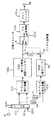
図1は、本発明の第1実施形態に係る波形発生装置の構成を示すブロック図である。図1において、信号系列が入力される入力端子91は、第1の帯域制限特性を有する波形発生装置2に接続されているとともに、スイッチ3を介してメモリ1に接続されている。波形発生装置2は、供給された信号系列に応じて第1の帯域制限特性で帯域制限された波形信号を発生させるものである。また、メモリ1には、供給された信号系列に対する第1の帯域制限特性で帯域制限された波形信号と、該信号系列に対する第2の帯域制限特性で帯域制限された波形信号との差分信号が予め演算により求められ、この差分信号が格納されている。波形発生装置2は、切換えスイッチ5の一方の被選択端子に接続されているとともに、スイッチ4を介して加算器6に接続されている。メモリ1はこの加算器6に接続されており、該加算器6は切換えスイッチ5の他方の被選択端子に接続されている。切換えスイッチ5の選択端子は出力端子96に接続されている。ここで、波形発生装置2、メモリ1、スイッチ4、および加算器6により第2の帯域制限特性を有する波形発生装置7が構成されている。
【0023】
次に、第1の帯域制限特性が要求される場合の動作について説明する。入力端子91から入力された信号系列は波形発生装置2に供給される。波形発生装置2では、供給された信号系列に応じて第1の帯域制限特性で帯域制限された波形信号が発生され、これが切換えスイッチ5を介して出力端子96から出力されるようになっている。なお、スイッチ3および4は開かれたままである。
【0024】
続いて、第2の帯域制限特性が要求される場合の動作について説明する。この場合には、スイッチ3および4が閉じられる。また、切換えスイッチ5が図中下側の被選択端子側に切換えられる。入力端子91から入力された信号系列は波形発生装置2に供給されるとともに、スイッチ3を介してメモリ1に供給される。波形発生装置2では、供給された信号系列に応じて第1の帯域制限特性で帯域制限された波形信号が発生され、これがスイッチ4を介して加算器6に供給される。メモリ1からは、供給された信号系列に応じて予め格納された差分信号(第1の帯域制限特性で帯域制限された波形信号と第2の帯域制限特性で帯域制限された波形信号との差分信号)が読み出され、これが加算器6に供給される。加算器6では、波形発生装置2からの波形信号とメモリ1からの差分信号との加算処理が行われ、この結果得られた第2の帯域制限特性で帯域制限された波形信号が切換えスイッチ5を介して出力端子96から出力されるようになっている。
【0025】
本実施形態の波形発生装置によれば、図3を参照しながら説明したように、メモリ1に格納する差分信号は帯域制限された出力波形の振幅値よりも遥かに小さいため、第2の帯域制限特性に対応した波形信号を格納する場合と比較してメモリ1の容量を大幅に削減することができ、同一機能を小さい回路規模で実現することができる。
【0026】
(第2実施形態)
図4は、本発明の第2実施形態に係る波形発生装置の構成を示すブロック図である。図4において、シンボル周期Tの信号系列が入力される入力端子91は、シフトレジスタ100に接続されている。シフトレジスタ100は、入力されたシンボル周期Tの信号系列をクロック信号CLK1(1/Tの周波数)に応じて順次シフトするものである。このシフトレジスタ100は、アドレス発生装置102aに接続されているとともに、スイッチ3aを介してアドレス発生装置102bに接続されている。また、第1および第2の帯域制限特性でのデータ補間率に対応したクロック信号CLK2(CLK1の自然数倍の周波数)をカウントするカウンタ101aは、アドレス発生装置102aに接続されているとともに、スイッチ3bを介してアドレス発生装置102bに接続されている。アドレス発生装置102aおよび102bは、それぞれシフトレジスタ100の出力およびカウンタ101aの出力に応じてアドレスデータを発生させるものである。アドレス発生装置102aは、第1の帯域制限特性を有する第1の帯域制限フィルタとしてのROM103aに接続されている。ROM103aには、第1の帯域制限特性で帯域制限された結果を示す波形データがnビット(nは自然数)精度で格納されている。このROM103aは、切換えスイッチ5の一方の被選択端子に接続されているとともに、スイッチ4を介してデジタル加算器41に接続されている。一方、アドレス発生装置102bは、ROM40に接続されている。ROM40には、第1の帯域制限特性で帯域制限された結果を示す波形データと第2の帯域制限特性で帯域制限された結果を示す波形データとの差分データがkビット(kは自然数であり、k<<n)精度で格納されている。このROM40はデジタル加算器41に接続されており、該デジタル加算器41は切換えスイッチ5の他方の被選択端子に接続されている。切換えスイッチ5の選択端子は、供給されたデジタルデータをクロック信号CLK2の周期でアナログ信号に変換するD/A変換器104aに接続されている。D/A変換器104aは折り返しノイズを除去するためのポストフィルタ105aに接続されており、該ポストフィルタ105aは出力端子96に接続されている。
【0027】
次に、第1の帯域制限特性が要求される場合の動作について説明する。この場合には、アドレス発生装置102b、ROM40、およびデジタル加算器41は動作させない。入力端子91から入力されたシンボル周期Tの信号系列はシフトレジスタ100に供給され、クロック信号CLK1に応じて順次シフトされる。アドレス発生装置102aには、このシフトレジスタ100からの出力が供給されるとともに、クロック信号CLK2をカウントするカウンタ101aからの出力が供給される。アドレス発生装置102aでは、シフトレジスタ100からの出力およびカウンタ101aからの出力に応じてアドレスデータが発生され、これがROM103aに供給される。ROM103aからは、供給されたアドレスデータに応じて、予め格納された波形データが読み出され、nビットのデジタルデータとして出力される。このデジタルデータは、切換えスイッチ5を介してD/A変換器104aに供給される。D/A変換器104aでは、供給されたデジタルデータがクロック信号CLK2の周期でアナログ信号に変換され、このアナログ信号がポストフィルタ105aに供給される。ポストフィルタ105aでは、供給されたアナログ信号から折り返しノイズが除去され、その結果得られた信号が出力端子96から、第1の帯域制限特性で帯域制限された信号として出力されるようになっている。なお、スイッチ3a、3bおよび4は開かれたままである。
【0028】
続いて、第2の帯域制限特性が要求される場合の動作について説明する。この場合には、スイッチ3a、3bおよび4が閉じられる。また、切換えスイッチ5が図中下側の被選択端子側に切換えられる。入力端子91から入力されたシンボル周期Tの信号系列はシフトレジスタ100に供給され、クロック信号CLK1に応じて順次シフトされる。アドレス発生装置102aには、このシフトレジスタ100からの出力が供給されるとともに、クロック信号CLK2をカウントするカウンタ101aからの出力が供給される。アドレス発生装置102aでは、シフトレジスタ100からの出力およびカウンタ101aからの出力に応じてアドレスデータが発生され、これがROM103aに供給される。ROM103aからは、供給されたアドレスデータに応じて、予め格納された波形データが読み出され、nビットのデジタルデータとして出力される。このデジタルデータは、スイッチ4を介してデジタル加算器41に供給される。一方、アドレス発生装置102bには、シフトレジスタ100からの出力がスイッチ3aを介して供給されるとともに、カウンタ101aからの出力がスイッチ3bを介して供給される。アドレス発生装置102bでは、シフトレジスタ100からの出力およびカウンタ101aからの出力に応じてアドレスデータが発生され、これがROM40に供給される。ROM40からは、供給されたアドレスデータに応じて、予め格納された差分データが読み出され、kビットのデジタルデータとして出力される。このデジタルデータは、デジタル加算器41に供給される。デジタル加算器41では、ROM103aからの波形データとROM40からの差分データとの加算処理が行われ、この加算結果が切換えスイッチ5を介してD/A変換器104aに供給される。D/A変換器104aでは、供給された加算結果(デジタルデータ)がクロック信号CLK2の周期でアナログ信号に変換され、このアナログ信号がポストフィルタ105aに供給される。ポストフィルタ105aでは、供給されたアナログ信号から折り返しノイズが除去され、その結果得られた信号が出力端子96から、第2の帯域制限特性で帯域制限された信号として出力されるようになっている。
【0029】
本実施形態の波形発生装置によれば、ROM40には差分データを格納しており、第2の帯域制限特性に対応した波形データを格納する場合と比較してROM40の容量を大幅に削減することができ、同一機能を小さい回路規模で実現することができる。
【0030】
(第3実施形態)
図5は、本発明の第3実施形態に係る波形発生装置の構成を示すブロック図である。図5において、シンボル周期Tの信号系列が入力される入力端子91は、シフトレジスタ100に接続されている。シフトレジスタ100は、入力されたシンボル周期Tの信号系列をクロック信号CLK1(1/Tの周波数)に応じて順次シフトするものである。このシフトレジスタ100は、アドレス発生装置102aに接続されているとともに、スイッチ3aを介してアドレス発生装置102bに接続されている。また、第1および第2の帯域制限特性でのデータ補間率に対応したクロック信号CLK2(CLK1の自然数倍の周波数)をカウントするカウンタ101aは、アドレス発生装置102aに接続されているとともに、スイッチ3bを介してアドレス発生装置102bに接続されている。アドレス発生装置102aおよび102bは、それぞれシフトレジスタ100の出力およびカウンタ101aの出力に応じてアドレスデータを発生させるものである。アドレス発生装置102aは、第1の帯域制限特性を有する第1の帯域制限フィルタとしてのROM103aに接続されている。ROM103aには、第1の帯域制限特性で帯域制限された結果を示す波形データがnビット(nは自然数)精度で格納されている。このROM103aは、供給されたデジタルデータをクロック信号CLK2の周期でアナログ信号に変換するD/A変換器104aに接続されている。D/A変換器104aは、切換えスイッチ5の一方の被選択端子に接続されているとともに、スイッチ4を介してアナログ加算器51に接続されている。一方、アドレス発生装置102bは、ROM40に接続されている。ROM40には、第1の帯域制限特性で帯域制限された結果を示す波形データと第2の帯域制限特性で帯域制限された結果を示す波形データとの差分データがkビット(kは自然数であり、k<<n)精度で格納されている。このROM40は、供給されたデジタルデータをクロック信号CLK2の周期でアナログ信号に変換するD/A変換器50に接続されている。D/A変換器50はアナログ加算器51に接続されており、該アナログ加算器51は切換えスイッチ5の他方の被選択端子に接続されている。切換えスイッチ5の選択端子は、折り返しノイズを除去するためのポストフィルタ105aに接続されており、該ポストフィルタ105aは出力端子96に接続されている。
【0031】
次に、第1の帯域制限特性が要求される場合の動作について説明する。この場合には、アドレス発生装置102b、ROM40、D/A変換器50、およびアナログ加算器51は動作させない。入力端子91から入力されたシンボル周期Tの信号系列はシフトレジスタ100に供給され、クロック信号CLK1に応じて順次シフトされる。アドレス発生装置102aには、このシフトレジスタ100からの出力が供給されるとともに、クロック信号CLK2をカウントするカウンタ101aからの出力が供給される。アドレス発生装置102aでは、シフトレジスタ100からの出力およびカウンタ101aからの出力に応じてアドレスデータが発生され、これがROM103aに供給される。ROM103aからは、供給されたアドレスデータに応じて、予め格納された波形データが読み出され、nビットのデジタルデータとして出力される。このデジタルデータは、D/A変換器104aに供給される。D/A変換器104aでは、供給されたデジタルデータがクロック信号CLK2の周期でアナログ信号に変換され、このアナログ信号が切換えスイッチ5を介してポストフィルタ105aに供給される。ポストフィルタ105aでは、供給されたアナログ信号から折り返しノイズが除去され、その結果得られた信号が出力端子96から、第1の帯域制限特性で帯域制限された信号として出力されるようになっている。なお、スイッチ3a、3bおよび4は開かれたままである。
【0032】
続いて、第2の帯域制限特性が要求される場合の動作について説明する。この場合には、スイッチ3a、3bおよび4が閉じられる。また、切換えスイッチ5が図中下側の被選択端子側に切換えられる。入力端子91から入力されたシンボル周期Tの信号系列はシフトレジスタ100に供給され、クロック信号CLK1に応じて順次シフトされる。アドレス発生装置102aには、このシフトレジスタ100からの出力が供給されるとともに、クロック信号CLK2をカウントするカウンタ101aからの出力が供給される。アドレス発生装置102aでは、シフトレジスタ100からの出力およびカウンタ101aからの出力に応じてアドレスデータが発生され、これがROM103aに供給される。ROM103aからは、供給されたアドレスデータに応じて、予め格納された波形データが読み出され、nビットのデジタルデータとして出力される。このデジタルデータは、D/A変換器104aに供給される。D/A変換器104aでは、供給されたデジタルデータがクロック信号CLK2の周期でアナログ信号に変換され、このアナログ信号がスイッチ4を介してアナログ加算器51に供給される。一方、アドレス発生装置102bには、シフトレジスタ100からの出力がスイッチ3aを介して供給されるとともに、カウンタ101aからの出力がスイッチ3bを介して供給される。アドレス発生装置102bでは、シフトレジスタ100からの出力およびカウンタ101aからの出力に応じてアドレスデータが発生され、これがROM40に供給される。ROM40からは、供給されたアドレスデータに応じて、予め格納された差分データが読み出され、kビットのデジタルデータとして出力される。このデジタルデータは、D/A変換器50に供給される。D/A変換器50では、供給されたデジタルデータがクロック信号CLK2の周期でアナログ信号に変換され、このアナログ信号がアナログ加算器51に供給される。アナログ加算器51では、D/A変換器104aからの波形データに基づくアナログ信号とD/A変換器50からの差分データに基づくアナログ信号との加算処理が行われ、この加算結果が切換えスイッチ5を介してポストフィルタ105aに供給される。ポストフィルタ105aでは、供給された加算結果から折り返しノイズが除去され、その結果得られた信号が出力端子96から、第2の帯域制限特性で帯域制限された信号として出力されるようになっている。
【0033】
本実施形態の波形発生装置によれば、ROM40には差分データを格納しており、第2の帯域制限特性に対応した波形データを格納する場合と比較してROM40の容量を大幅に削減することができ、同一機能を小さい回路規模で実現することができる。
【0034】
また、本実施形態の波形発生装置によれば、ROM103aからの波形データとROM40からの差分データをそれぞれアナログ信号に変換してから加算するようにしているため、ROM40に格納する差分データのビット精度とD/A変換器50の分解能を調整することができる。従って、第2の帯域制限特性を有する波形発生装置を独立に設ける場合に比べて、D/A変換器50の分解能を小さくすることができ、更に回路規模を小さくすることができる。
【0035】
(第4実施形態)
図6は、本発明の第4実施形態に係る波形発生装置の構成を示すブロック図である。図6において、シンボル周期Tの信号系列が入力される入力端子91は、シフトレジスタ100に接続されている。シフトレジスタ100は、入力されたシンボル周期Tの信号系列をクロック信号CLK1(1/Tの周波数)に応じて順次シフトするものである。このシフトレジスタ100は、アドレス発生装置102aに接続されているとともに、スイッチ3を介してアドレス発生装置61に接続されている。また、第1の帯域制限特性でのデータ補間率に対応したクロック信号CLK2(CLK1の自然数倍の周波数)をカウントするカウンタ101aは、アドレス発生装置102aに接続されている。アドレス発生装置102aは、シフトレジスタ100の出力およびカウンタ101aの出力に応じてアドレスデータを発生させるものである。アドレス発生装置102aは、第1の帯域制限特性を有する第1の帯域制限フィルタとしてのROM103aに接続されている。ROM103aには、第1の帯域制限特性で帯域制限された結果を示す波形データがnビット(nは自然数)精度で、クロック信号CLK2に対応したデータ補間率で格納されている。このROM103aは、供給されたデジタルデータをクロック信号CLK2の周期でアナログ信号に変換するD/A変換器104aに接続されている。D/A変換器104aは、折り返しノイズを除去するためのポストフィルタ105aに接続されているとともに、スイッチ4を介してアナログ加算器51に接続されている。ポストフィルタ105aは、切換えスイッチ5の一方の被選択端子に接続されている。一方、第2の帯域制限特性でのデータ補間率に対応したクロック信号CLK3(CLK1の自然数倍の周波数)をカウントするカウンタ60は、アドレス発生装置61に接続されている。アドレス発生装置61は、シフトレジスタ100の出力およびカウンタ60の出力に応じてアドレスデータを発生させるものである。アドレス発生装置61は、ROM62に接続されている。ROM62には、第1の帯域制限特性で帯域制限された結果を示す波形データと第2の帯域制限特性で帯域制限された結果を示す波形データとの差分データがkビット(kは自然数であり、k<<n)精度で、クロック信号CLK3に対応したデータ補間率で格納されている。このROM62は、供給されたデジタルデータをクロック信号CLK3の周期でアナログ信号に変換するD/A変換器50に接続されている。D/A変換器50はアナログ加算器51に接続されており、該アナログ加算器51は、折り返しノイズを除去するためのポストフィルタ63に接続されている。ポストフィルタ63は、切換えスイッチ5の他方の被選択端子に接続されている。切換えスイッチ5の選択端子は、出力端子96に接続されている。
【0036】
次に、第1の帯域制限特性が要求される場合の動作について説明する。この場合には、カウンタ60、アドレス発生装置61、ROM62、D/A変換器50、アナログ加算器51およびポストフィルタ63は動作させない。入力端子91から入力されたシンボル周期Tの信号系列はシフトレジスタ100に供給され、クロック信号CLK1に応じて順次シフトされる。アドレス発生装置102aには、このシフトレジスタ100からの出力が供給されるとともに、クロック信号CLK2をカウントするカウンタ101aからの出力が供給される。アドレス発生装置102aでは、シフトレジスタ100からの出力およびカウンタ101aからの出力に応じてアドレスデータが発生され、これがROM103aに供給される。ROM103aからは、供給されたアドレスデータに応じて、予め格納された波形データが読み出され、nビットのデジタルデータとして出力される。このデジタルデータは、D/A変換器104aに供給される。D/A変換器104aでは、供給されたデジタルデータがクロック信号CLK2の周期でアナログ信号に変換され、このアナログ信号がポストフィルタ105aに供給される。ポストフィルタ105aでは、供給されたアナログ信号から折り返しノイズが除去され、その結果得られた信号が切換えスイッチ5を介して出力端子96から、第1の帯域制限特性で帯域制限された信号として出力されるようになっている。なお、スイッチ3および4は開かれたままである。
【0037】
続いて、第2の帯域制限特性が要求される場合の動作について説明する。この場合には、スイッチ3および4が閉じられる。また、切換えスイッチ5が図中下側の被選択端子側に切換えられる。入力端子91から入力されたシンボル周期Tの信号系列はシフトレジスタ100に供給され、クロック信号CLK1に応じて順次シフトされる。アドレス発生装置102aには、このシフトレジスタ100からの出力が供給されるとともに、クロック信号CLK2をカウントするカウンタ101aからの出力が供給される。アドレス発生装置102aでは、シフトレジスタ100からの出力およびカウンタ101aからの出力に応じてアドレスデータが発生され、これがROM103aに供給される。ROM103aからは、供給されたアドレスデータに応じて、予め格納された波形データが読み出され、nビットのデジタルデータとして出力される。このデジタルデータは、D/A変換器104aに供給される。D/A変換器104aでは、供給されたデジタルデータがクロック信号CLK2の周期でアナログ信号に変換され、このアナログ信号がスイッチ4を介してアナログ加算器51に供給される。一方、アドレス発生装置61には、シフトレジスタ100からの出力がスイッチ3を介して供給されるとともに、クロック信号CLK3をカウントするカウンタ60からの出力が供給される。アドレス発生装置61では、シフトレジスタ100からの出力およびカウンタ60からの出力に応じてアドレスデータが発生され、これがROM62に供給される。ROM62からは、供給されたアドレスデータに応じて、予め格納された差分データが読み出され、kビットのデジタルデータとして出力される。このデジタルデータは、D/A変換器50に供給される。D/A変換器50では、供給されたデジタルデータがクロック信号CLK3の周期でアナログ信号に変換され、このアナログ信号がアナログ加算器51に供給される。アナログ加算器51では、D/A変換器104aからの波形データに基づくアナログ信号とD/A変換器50からの差分データに基づくアナログ信号との加算処理が行われ、この加算結果がポストフィルタ63に供給される。ポストフィルタ63では、供給された加算結果から折り返しノイズが除去され、その結果得られた信号が切換えスイッチ5を介して出力端子96から、第2の帯域制限特性で帯域制限された信号として出力されるようになっている。
【0038】
本実施形態の波形発生装置によれば、ROM62には差分データを格納しており、第2の帯域制限特性に対応した波形データを格納する場合と比較してROM62の容量を大幅に削減することができ、同一機能を小さい回路規模で実現することができる。
【0039】
また、本実施形態の波形発生装置によれば、ROM103aからの波形データとROM62からの差分データをそれぞれアナログ信号に変換してから加算するようにしているため、ROM62に格納する差分データのビット精度とデータ補間率、D/A変換器50の分解能と入力クロック信号を調整することができる。従って、第2の帯域制限特性を有する波形発生装置を独立に設ける場合に比べて、D/A変換器50の分解能を小さくすることができ、更に回路規模を小さくすることができる。
【0040】
(第5実施形態)
図7は、本発明の第5実施形態に係る波形発生装置の構成を示すブロック図である。図7において、シンボル周期Tの信号系列が入力される入力端子91は、シフトレジスタ100に接続されている。シフトレジスタ100は、入力されたシンボル周期Tの信号系列をクロック信号CLK1(1/Tの周波数)に応じて順次シフトするものである。このシフトレジスタ100は、アドレス発生装置102aに接続されているとともに、スイッチ3を介してアドレス発生装置61に接続されている。また、第1の帯域制限特性でのデータ補間率に対応したクロック信号CLK2(CLK1の自然数倍の周波数)をカウントするカウンタ101aは、アドレス発生装置102aに接続されている。アドレス発生装置102aは、シフトレジスタ100の出力およびカウンタ101aの出力に応じてアドレスデータを発生させるものである。アドレス発生装置102aは、第1の帯域制限特性を有する第1の帯域制限フィルタとしてのROM103aに接続されている。ROM103aには、第1の帯域制限特性で帯域制限された結果を示す波形データがnビット(nは自然数)精度で、クロック信号CLK2に対応したデータ補間率で格納されている。このROM103aは、切換えスイッチ72の一方の被選択端子に接続されているとともに、スイッチ4を介して補間フィルタ70に接続されている。補間フィルタ70は、ROM103aから出力される波形データの、クロック信号CLK2に対応したデータ補間率をクロック信号CLK3に対応したデータ補間率に変換するフィルタである。この補間フィルタ70は、デジタル加算器71に接続されている。一方、第2の帯域制限特性でのデータ補間率に対応したクロック信号CLK3(CLK1の自然数倍の周波数)をカウントするカウンタ60は、アドレス発生装置61に接続されている。アドレス発生装置61は、シフトレジスタ100の出力およびカウンタ60の出力に応じてアドレスデータを発生させるものである。アドレス発生装置61は、ROM62に接続されている。ROM62には、第1の帯域制限特性で帯域制限された結果を示す波形データと第2の帯域制限特性で帯域制限された結果を示す波形データとの差分データがkビット(kは自然数であり、k<<n)精度で、クロック信号CLK3に対応したデータ補間率で格納されている。このROM62はデジタル加算器71に接続されており、該デジタル加算器71は切換えスイッチ72の他方の被選択端子に接続されている。切換えスイッチ72の選択端子はD/A変換器104aに接続されている。D/A変換器104aには、該D/A変換器104aにクロック信号CLK2およびCLK3のいずれか一方を供給するための切換えスイッチ73が接続されている。D/A変換器104aは、供給されたデジタルデータを切換えスイッチ73からのクロック信号の周期でアナログ信号に変換するものである。このD/A変換器104aは、クロック信号CLK2に対応したデータ補間率で発生する折り返しノイズを除去するためのポストフィルタ105aに接続されているとともに、スイッチ74を介してクロック信号CLK3に対応したデータ補間率で発生する折り返しノイズを除去するためのポストフィルタ63に接続されている。ポストフィルタ105aは、切換えスイッチ5の一方の被選択端子に接続されており、ポストフィルタ63は、切換えスイッチ5の他方の被選択端子に接続されている。切換えスイッチ5の選択端子は、出力端子96に接続されている。
【0041】
次に、第1の帯域制限特性が要求される場合の動作について説明する。この場合には、カウンタ60、アドレス発生装置61、ROM62、補間フィルタ70、デジタル加算器71およびポストフィルタ63は動作させない。入力端子91から入力されたシンボル周期Tの信号系列はシフトレジスタ100に供給され、クロック信号CLK1に応じて順次シフトされる。アドレス発生装置102aには、このシフトレジスタ100からの出力が供給されるとともに、クロック信号CLK2をカウントするカウンタ101aからの出力が供給される。アドレス発生装置102aでは、シフトレジスタ100からの出力およびカウンタ101aからの出力に応じてアドレスデータが発生され、これがROM103aに供給される。ROM103aからは、供給されたアドレスデータに応じて、予め格納された波形データが読み出され、nビットのデジタルデータとして出力される。このデジタルデータは、切換えスイッチ72を介してD/A変換器104aに供給される。D/A変換器104aでは、供給されたデジタルデータが切換えスイッチ73からのクロック信号CLK2の周期でアナログ信号に変換され、このアナログ信号がポストフィルタ105aに供給される。ポストフィルタ105aでは、供給されたアナログ信号から折り返しノイズが除去され、その結果得られた信号が切換えスイッチ5を介して出力端子96から、第1の帯域制限特性で帯域制限された信号として出力されるようになっている。なお、スイッチ3、4および74は開かれたままである。
【0042】
続いて、第2の帯域制限特性が要求される場合の動作について説明する。この場合には、スイッチ3、4および74が閉じられる。また、切換えスイッチ72が図中下側の被選択端子側に切換えられ、切換えスイッチ73が図中右側の被選択端子側に切換えられるとともに、切換えスイッチ5が図中下側の被選択端子側に切換えられる。入力端子91から入力されたシンボル周期Tの信号系列はシフトレジスタ100に供給され、クロック信号CLK1に応じて順次シフトされる。アドレス発生装置102aには、このシフトレジスタ100からの出力が供給されるとともに、クロック信号CLK2をカウントするカウンタ101aからの出力が供給される。アドレス発生装置102aでは、シフトレジスタ100からの出力およびカウンタ101aからの出力に応じてアドレスデータが発生され、これがROM103aに供給される。ROM103aからは、供給されたアドレスデータに応じて、予め格納された波形データが読み出され、nビットのデジタルデータとして出力される。このデジタルデータは、スイッチ4を介して補間フィルタ70に供給され、クロック信号CLK2に対応したデータ補間率がクロック信号CLK3に対応したデータ補間率に変換される。データ補間率が変換されたデータは、デジタル加算器71に供給される。一方、アドレス発生装置61には、シフトレジスタ100からの出力がスイッチ3を介して供給されるとともに、クロック信号CLK3をカウントするカウンタ60からの出力が供給される。アドレス発生装置61では、シフトレジスタ100からの出力およびカウンタ60からの出力に応じてアドレスデータが発生され、これがROM62に供給される。ROM62からは、供給されたアドレスデータに応じて、予め格納された差分データが読み出され、kビットのデジタルデータとして出力される。このデジタルデータはデジタル加算器71に供給される。デジタル加算器71では、補間フィルタ70からのデータ補間率が変換された波形データとROM62からの差分データとの加算処理が行われ、この加算結果が切換えスイッチ72を介してD/A変換器104aに供給される。D/A変換器104aでは、供給された加算結果(デジタルデータ)が切換えスイッチ73からのクロック信号CLK3の周期でアナログ信号に変換され、このアナログ信号がスイッチ74を介してポストフィルタ63に供給される。ポストフィルタ63では、供給されたアナログ信号から折り返しノイズが除去され、その結果得られた信号が切換えスイッチ5を介して出力端子96から、第2の帯域制限特性で帯域制限された信号として出力されるようになっている。
【0043】
本実施形態の波形発生装置によれば、ROM62には差分データを格納しており、第2の帯域制限特性に対応した波形データを格納する場合と比較してROM62の容量を大幅に削減することができ、同一機能を小さい回路規模で実現することができる。
【0044】
また、本実施形態の波形発生装置によれば、補間フィルタ70を挿入することにより、D/A変換器104aを共有できるようにしているため、第2の帯域制限特性を有する波形発生装置を独立に設ける場合に比べて、更に回路規模を小さくすることができる。
【0045】
なお、本実施形態では、ROM103aから出力される波形データについて、クロック信号CLK2に対応したデータ補間率をクロック信号CLK3に対応したデータ補間率に変換する補間フィルタ70が設けられているが、この補間フィルタ70の替わりに、ROM62から出力される差分データについて、クロック信号CLK3に対応したデータ補間率をクロック信号CLK2に対応したデータ補間率に変換する補間フィルタを設けるようにしてもよい。
【0046】
(第6実施形態)
図8は、本発明の第6実施形態に係る直交変調用波形発生装置の構成を示すブロック図である。図8において、シリアル送信データが入力される入力端子91は、該シリアル送信データをパラレルデータに変換するシリアル/パラレル変換装置80に接続されている。このシリアル/パラレル変換装置80は、マッピング装置81に接続されている。マッピング装置81は、シリアル/パラレル変換装置80からのパラレルデータを振幅位相情報に変換し、IチャネルのシンボルデータおよびQチャネルのシンボルデータとして出力するものである。このマッピング装置81は、第1の帯域制限特性を有する波形発生装置2aに接続されているとともに、スイッチ3aを介してメモリ1aに接続されている。波形発生装置2aは、供給されたIチャネルのシンボルデータに応じて第1の帯域制限特性で帯域制限された波形信号を発生させるものである。また、メモリ1aには、供給されたIチャネルのシンボルデータに対する第1の帯域制限特性で帯域制限された波形信号と、該シンボルデータに対する第2の帯域制限特性で帯域制限された波形信号との差分信号が予め演算により求められ、この差分信号が格納されている。波形発生装置2aは、切換えスイッチ5aの一方の被選択端子に接続されているとともに、スイッチ4aを介して加算器6aに接続されている。メモリ1aはこの加算器6aに接続されており、該加算器6aは切換えスイッチ5aの他方の被選択端子に接続されている。切換えスイッチ5aの選択端子は出力端子96aに接続されている。ここで、波形発生装置2a、メモリ1a、スイッチ4a、および加算器6aにより第2の帯域制限特性を有する波形発生装置7aが構成されている。また、マッピング装置81は、第1の帯域制限特性を有する波形発生装置2bに接続されているとともに、スイッチ3bを介してメモリ1bに接続されている。波形発生装置2bは、供給されたQチャネルのシンボルデータに応じて第1の帯域制限特性で帯域制限された波形信号を発生させるものである。また、メモリ1bには、供給されたQチャネルのシンボルデータに対する第1の帯域制限特性で帯域制限された波形信号と、該シンボルデータに対する第2の帯域制限特性で帯域制限された波形信号との差分信号が予め演算により求められ、この差分信号が格納されている。波形発生装置2bは、切換えスイッチ5bの一方の被選択端子に接続されているとともに、スイッチ4bを介して加算器6bに接続されている。メモリ1bはこの加算器6bに接続されており、該加算器6bは切換えスイッチ5bの他方の被選択端子に接続されている。切換えスイッチ5bの選択端子は出力端子96bに接続されている。ここで、波形発生装置2b、メモリ1b、スイッチ4b、および加算器6bにより第2の帯域制限特性を有する波形発生装置7bが構成されている。
【0047】
次に、第1の帯域制限特性が要求される場合の動作について説明する。この場合には、メモリ1a、1bおよび加算器6a、6bは動作させない。入力端子91から入力されたシリアル送信データはシリアル/パラレル変換装置80に供給される。シリアル/パラレル変換装置80では、供給されたシリアル送信データがパラレルデータに変換されて、これがマッピング装置81に供給される。マッピング装置81では、供給されたパラレルデータが振幅位相情報に変換され、IチャネルのシンボルデータおよびQチャネルのシンボルデータとして出力される。Iチャネルのシンボルデータは波形発生装置2aに供給される。波形発生装置2aでは、供給されたIチャネルのシンボルデータに応じて第1の帯域制限特性で帯域制限された波形信号が発生され、これが切換えスイッチ5aを介して出力端子96aから出力されるようになっている。一方、マッピング装置81からのQチャネルのシンボルデータは波形発生装置2bに供給される。波形発生装置2bでは、供給されたQチャネルのシンボルデータに応じて第1の帯域制限特性で帯域制限された波形信号が発生され、これが切換えスイッチ5bを介して出力端子96bから出力されるようになっている。なお、スイッチ3a、3bおよび4a、4bは開かれたままである。
【0048】
続いて、第2の帯域制限特性が要求される場合の動作について説明する。この場合には、スイッチ3a、3bおよび4a、4bが閉じられる。また、切換えスイッチ5a、5bがそれぞれ図中下側の被選択端子側に切換えられる。入力端子91から入力されたシリアル送信データはシリアル/パラレル変換装置80に供給される。シリアル/パラレル変換装置80では、供給されたシリアル送信データがパラレルデータに変換されて、これがマッピング装置81に供給される。マッピング装置81では、供給されたパラレルデータが振幅位相情報に変換され、IチャネルのシンボルデータおよびQチャネルのシンボルデータとして出力される。Iチャネルのシンボルデータは波形発生装置2aに供給されるとともに、スイッチ3aを介してメモリ1aに供給される。波形発生装置2aでは、供給されたIチャネルのシンボルデータに応じて第1の帯域制限特性で帯域制限された波形信号が発生され、これがスイッチ4aを介して加算器6aに供給される。メモリ1aからは、供給されたIチャネルのシンボルデータに応じて予め格納された差分信号が読み出され、これが加算器6aに供給される。加算器6aでは、波形発生装置2aからの波形信号とメモリ1aからの差分信号との加算処理が行われ、この結果得られた第2の帯域制限特性で帯域制限された波形信号が切換えスイッチ5aを介して出力端子96aから出力されるようになっている。一方、マッピング装置81からのQチャネルのシンボルデータは波形発生装置2bに供給されるとともに、スイッチ3bを介してメモリ1bに供給される。波形発生装置2bでは、供給されたQチャネルのシンボルデータに応じて第1の帯域制限特性で帯域制限された波形信号が発生され、これがスイッチ4bを介して加算器6bに供給される。メモリ1bからは、供給されたQチャネルのシンボルデータに応じて予め格納された差分信号が読み出され、これが加算器6b供給される。加算器6bでは、波形発生装置2bからの波形信号とメモリ1bからの差分信号との加算処理が行われ、この結果得られた第2の帯域制限特性で帯域制限された波形信号が切換えスイッチ5bを介して出力端子96bから出力されるようになっている。
【0049】
本実施形態の直交変調用波形発生装置によれば、メモリ1a、1bには差分信号を格納しており、第2の帯域制限特性に対応した波形信号を格納する場合と比較してメモリ1a、1bの容量を大幅に削減することができ、同一機能を小さい回路規模で実現することができる。
【0050】
なお、本実施形態の構成において、Iチャネル用の波形発生装置とQチャネル用の波形発生装置を時分割的に用いるようにすることも可能である。
【0051】
【発明の効果】
上述した説明から明らかなように、本発明によれば、メモリ手段に格納する差分信号(差分データ)は帯域制限された出力波形の振幅値よりも遥かに小さいため、第2の帯域制限特性に対応した波形信号(波形データ)を格納する場合と比較してメモリ手段の容量を大幅に削減することができる。従って、複数の帯域制限特性に対応して動作可能な波形発生装置を小さい回路規模で実現することができる。
【図面の簡単な説明】
【図1】本発明の第1実施形態に係る波形発生装置の構成を示すブロック図である。
【図2】ロールオフフィルタのインパルス応答を示す波形図である。
【図3】入力信号系列に対するロールオフフィルタの出力を示す波形図である。
【図4】本発明の第2実施形態に係る波形発生装置の構成を示すブロック図である。
【図5】本発明の第3実施形態に係る波形発生装置の構成を示すブロック図である。
【図6】本発明の第4実施形態に係る波形発生装置の構成を示すブロック図である。
【図7】本発明の第5実施形態に係る波形発生装置の構成を示すブロック図である。
【図8】本発明の第6実施形態に係る直交変調用波形発生装置の構成を示すブロック図である。
【図9】従来の波形発生装置の一例を示すブロック図である。
【図10】図9に示した波形発生装置の具体的な構成例を示すブロック図である。
【図11】図9に示した波形発生装置の他の具体的な構成例を示すブロック図である。
【符号の説明】
1、1a、1b メモリ
2、2a、2b、7、7a、7b 波形発生装置
5、5a、5b、72、73 切換えスイッチ
6、6a、6b 加算器
40、62 ROM
41、71 デジタル加算器
50、104a、104b D/A変換器
51 アナログ加算器
61、102a、102b アドレス発生装置
63、105a ポストフィルタ
70 補間フィルタ
80 シリアル/パラレル変換装置
81 マッピング装置[0001]
BACKGROUND OF THE INVENTION
The present invention relates to a waveform generator that is provided in a mobile communication terminal device and can operate in accordance with a plurality of band limiting characteristics in a modulation device for modulating a digital signal.
[0002]
[Prior art]
In recent years, digitalization technology is indispensable for accurately transmitting more information as communication and broadcasting are digitized. In addition, with the advancement of LSI (Large Scale Integrated Circuit) technology, functions and systems that have been configured with a plurality of chips so far tend to be integrated on one chip. Under such a background, in the mobile communication field, there is a demand for a shared terminal device that can support a plurality of communication systems with a single terminal device. In general, the characteristics of band-limiting filters that are indispensable for modulators are defined by the standards of each communication system, but are different from each other, and therefore it is necessary to provide a waveform generator having a plurality of band-limiting characteristics in a shared terminal device. is there.
[0003]
By the way, when transmitting a digital signal with band limitation, a roll-off filter is used to prevent interference (intersymbol interference) between the digital signals caused by the band limitation filter. Here, the case where the band limiting characteristics are different is the case where the roll-off rates for determining the cutoff characteristics are different, or the case where the characteristic functions themselves are different as in the Nyquist filter and the root Nyquist filter. 2A shows an impulse response waveform (for ± 3 symbol periods) of a Nyquist filter with roll-off rates (α) of 0.5 and 0.25, and FIG. 2B shows the roll-off rate. Are both impulse response waveforms (± 3 symbol periods) of the Nyquist filter and the root Nyquist filter of 0.5. As is clear from the figure, the roll-off filter has a common characteristic that the center amplitude of the impulse response waveform is around 1 and the amplitude is around 0 at the remaining symbol points. This property enables accurate transmission of information while suppressing intersymbol interference with the input signal sequence. 3 (a) and 3 (b) show the binary signal sequence {-1, -1, -1, -1, +1, +1, +1) with the band limiting characteristics shown in FIGS. 2 (a) and 2 (b). }, The difference between the output waveforms and the amplitude value between the output waveforms (difference signal) when the total 7 symbols are band-limited. As is apparent from the figure, in the output waveform when the band is limited by any band limiting characteristic, it passes near the amplitude value of the symbol value input at each symbol point. As a result, even if the band limiting characteristics are slightly different, the differential signal is much smaller than the amplitude value of each output waveform.
[0004]
The roll-off filter as described above can be realized by a digital filter, but the circuit scale becomes large because a plurality of digital multipliers are used. Therefore, a configuration using a ROM (Read Only Memory) is generally used as a means for realizing a small circuit scale.
[0005]
In a roll-off filter using a ROM, a convolution operation is performed in advance between an impulse response and an input signal series according to the band limiting characteristic, and the result is stored in the ROM. Then, data (convolution result) is read from the ROM in accordance with the input signal series, and is output as a band-limited signal. Since a calculation result corresponding to the band limiting characteristic is stored in the ROM, when a roll-off filter having a plurality of band limiting characteristics is required, it is necessary to provide a plurality of ROMs.
[0006]
FIG. 9 is a block diagram showing an example of a conventional waveform generator that can operate in accordance with a plurality of band limiting characteristics. In this figure, the waveform generator is provided with a
[0007]
FIG. 10 is a block diagram showing a specific configuration example of the waveform generator shown in FIG. In this configuration example, the first band-limiting filter and the second band-limiting filter have different band-limiting characteristics, data interpolation rate at the time of calculation, and bit accuracy of the calculation result. In FIG. 10, a
[0008]
Next, an operation when the first band limitation characteristic is required will be described. A signal sequence having a symbol period T input from the
[0009]
Next, an operation when the second band limitation characteristic is required will be described. In this case, the
[0010]
FIG. 11 is a block diagram illustrating another specific configuration example of the waveform generator illustrated in FIG. 9. In this configuration example, the first band-limiting filter and the second band-limiting filter have the same data interpolation rate at the time of calculation and the bit accuracy of the calculation result, but differ only in the band-limiting characteristics. In FIG. 11, a
[0011]
Next, an operation when the first band limitation characteristic is required will be described. A signal sequence having a symbol period T input from the
[0012]
Next, an operation when the second band limitation characteristic is required will be described. In this case, the changeover switches 94 and 95 are changed over. The address data from the
[0013]
[Problems to be solved by the invention]
As described above, when the first band-limiting filter and the second band-limiting filter have the same data interpolation rate at the time of calculation and the bit precision of the calculation result, but only the band-limiting characteristics are different, the results are shown in FIG. By adopting such a configuration, the circuit scale can be made somewhat smaller than that shown in FIG. However, in any case, it is necessary to provide two band limiting filters, and even if these filters are realized by a ROM, the circuit scale cannot be reduced so much.
[0014]
The present invention has been made in view of such conventional problems, and an object of the present invention is to provide a waveform generator with a small circuit scale that can operate in accordance with a plurality of band limiting characteristics.
[0015]
[Means for Solving the Problems]
In order to achieve the above-described object, first, a waveform generator of the present invention is a waveform generator operable in accordance with a plurality of band limiting characteristics, and has a first band limiting characteristic according to an input signal sequence. Waveform generating means for generating a band-limited waveform signal, a waveform signal band-limited by a first band-limiting characteristic for the input signal series, and band-limited by a second band-limiting characteristic for the input signal series A difference signal with respect to the waveform signal is stored in advance, and a memory means for outputting the difference signal in accordance with the input signal series, and an addition process of the waveform signal from the waveform generation means and the difference signal from the memory means And selecting one of the addition means for outputting the waveform signal band-limited by the second band-limiting characteristic, and the waveform signal from the waveform generation means and the waveform signal from the addition means It is characterized by comprising and a changeover switch means for outputting the.
[0016]
Second, the waveform generator of the present invention is a waveform generator operable in accordance with a plurality of band limiting characteristics, a first address generator for generating address data in accordance with an input signal sequence, Waveform data indicating a result of band limitation by the band limitation characteristic of the first memory means for outputting the waveform data in accordance with address data from the first address generating means, and the input A second address generating means for generating address data in accordance with the signal series; waveform data indicating a result of band limitation by the first band limiting characteristic; and a waveform indicating a result of band limiting by the second band limiting characteristic. Differential data is stored in advance, and second memory means for outputting the differential data in response to address data from the second address generating means; Digital addition means for performing addition processing of the waveform data from the memory means and the difference data from the second memory means, and outputting waveform data indicating the result of band limitation by the second band limitation characteristic; Digital / analog conversion means for converting either waveform data from one memory means or waveform data from the digital addition means into an analog signal, and aliasing noise is removed from the analog signal from the digital / analog conversion means. And filter means for outputting the output.
[0017]
Thirdly, the waveform generator of the present invention is a waveform generator operable in accordance with a plurality of band limiting characteristics, a first address generating means for generating address data in accordance with an input signal sequence, Waveform data indicating a result of band limitation by the band limitation characteristic of the first address is stored in advance, and first memory means for outputting the waveform data in accordance with address data from the first address generation means, and the first memory means First digital / analog converting means for converting waveform data from one memory means into an analog signal, second address generating means for generating address data in accordance with the input signal series, and first band limiting characteristics Difference data between the waveform data indicating the result of band limitation in FIG. 5 and the waveform data indicating the result of band limitation with the second band limitation characteristic is stored in advance, and the second data Second memory means for outputting the difference data in response to address data from a dress generation means; second digital / analog conversion means for converting the difference data from the second memory means into an analog signal; Addition processing of the analog signal based on the waveform data from the first digital / analog conversion means and the analog signal based on the difference data from the second digital / analog conversion means is performed, and the band is limited by the second band limiting characteristic. The analog addition means for outputting an analog signal corresponding to the waveform data indicating the result obtained, and the aliasing noise from any one of the analog signal from the first digital / analog conversion means and the analog signal from the analog addition means And a filter means for removing and outputting.
[0018]
Fourth, the waveform generator of the present invention is a waveform generator operable in accordance with a plurality of band limiting characteristics, a first address generating means for generating address data in accordance with an input signal sequence, Waveform data indicating the result of the band limitation by the band limitation characteristic is stored in advance at the first data interpolation rate, and the waveform data is output according to the address data from the first address generation means. Memory means, first digital / analog conversion means for converting the waveform data from the first memory means into an analog signal at a cycle of a first clock signal corresponding to a first data interpolation rate, and the input Second address generating means for generating address data in accordance with the signal series, waveform data indicating a result of band limitation by the first band limiting characteristic, and band control by the second band limiting characteristic. Difference data with the waveform data indicating the result is stored in advance at a second data interpolation rate, and second memory means for outputting the difference data in accordance with address data from the second address generating means Second digital / analog conversion means for converting the difference data from the second memory means into an analog signal at a cycle of a second clock signal corresponding to a second data interpolation rate; and the first digital An addition process of the analog signal based on the waveform data from the analog / analog conversion means and the analog signal based on the difference data from the second digital / analog conversion means is performed, and the result of band limitation by the second band limitation characteristic is obtained. An analog adding means for outputting an analog signal corresponding to the waveform data shown, and an analog signal from the first digital / analog converting means. From the first filter means for removing noise, the second filter means for removing aliasing noise from the analog signal from the analog adder means, the signal from the first filter means, and the second filter means Changeover switch means for selectively outputting any one of the above signals.
[0019]
Fifth, the waveform generator of the present invention is a waveform generator operable in accordance with a plurality of band limiting characteristics, a first address generating means for generating address data in accordance with an input signal sequence, Waveform data indicating the result of the band limitation by the band limitation characteristic is stored in advance at the first data interpolation rate, and the waveform data is output according to the address data from the first address generation means. Memory means, second address generating means for generating address data in accordance with the input signal series, waveform data indicating the result of band limitation by the first band limiting characteristic, and band by the second band limiting characteristic Difference data from the waveform data indicating the limited result is stored in advance at the second data interpolation rate, and the difference data is determined according to the address data from the second address generation means. From the first memory means, the interpolation filter means for converting the first data interpolation rate of the waveform data output from the first memory means into the second data interpolation rate, and the interpolation filter means Digital that performs addition processing of the waveform data converted to the second data interpolation rate and the difference data from the second memory means, and outputs waveform data indicating the result of band limitation by the second band limitation characteristic An adder; and a digital / analog converter that converts any one of the waveform data from the first memory and the waveform data from the digital adder into an analog signal at a cycle of a clock signal corresponding to a data interpolation rate; When the analog signal from the digital / analog converting means is based on the data of the first data interpolation rate, the analog signal is turned back from the analog signal. First filter means for removing noise and a second filter for removing aliasing noise from the analog signal when the analog signal from the digital / analog converting means is based on the data of the second data interpolation rate And a changeover switch means for selectively outputting one of the signal from the first filter means and the signal from the second filter means.
[0020]
Sixth, the waveform generator of the present invention is a quadrature modulation waveform generator operable in accordance with a plurality of band limiting characteristics, a serial / parallel converter for converting serial transmission data into parallel data, and the serial / Parallel conversion means for converting parallel data from the conversion means into amplitude and phase information and outputting as I-channel symbol data and Q-channel symbol data, and first data corresponding to the I-channel symbol data from the mapping means First waveform generating means for generating a waveform signal band-limited by the band-limiting characteristic, a waveform signal band-limited by the first band-limiting characteristic for the I channel symbol data, and a second waveform signal for the symbol data A differential signal from the waveform signal band-limited by the band-limiting characteristic is stored in advance, and First memory means for outputting the difference signal in accordance with the volume data, addition processing of the waveform signal from the first waveform generation means and the difference signal from the first memory means, and a second band A first adding means for outputting a waveform signal whose band is limited by the limiting characteristic, and selectively outputting one of the waveform signal from the first waveform generating means and the waveform signal from the first adding means. First switching switch means, second waveform generating means for generating a waveform signal band-limited by a first band-limiting characteristic in accordance with Q channel symbol data from the mapping means, A differential signal between the waveform signal band-limited by the first band-limiting characteristic for the symbol data and the waveform signal band-limited by the second band-limiting characteristic for the symbol data is stored in advance. Second memory means for outputting the difference signal in accordance with the symbol data, and addition processing of the waveform signal from the second waveform generation means and the difference signal from the second memory means. A second adding means for outputting a waveform signal band-limited by the second band-limiting characteristic, a waveform signal from the second waveform generating means, and a waveform signal from the second adding means. And a second changeover switch means for selectively outputting one of them.
[0021]
DETAILED DESCRIPTION OF THE INVENTION
Hereinafter, embodiments of the present invention will be described in detail with reference to the drawings.
[0022]
(First embodiment)
FIG. 1 is a block diagram showing the configuration of the waveform generator according to the first embodiment of the present invention. In FIG. 1, an
[0023]
Next, an operation when the first band limitation characteristic is required will be described. The signal series input from the
[0024]
Next, an operation when the second band limitation characteristic is required will be described. In this case, switches 3 and 4 are closed. Further, the
[0025]
According to the waveform generator of this embodiment, as described with reference to FIG. 3, the difference signal stored in the
[0026]
(Second Embodiment)
FIG. 4 is a block diagram showing a configuration of a waveform generator according to the second embodiment of the present invention. In FIG. 4, an
[0027]
Next, an operation when the first band limitation characteristic is required will be described. In this case, the
[0028]
Next, an operation when the second band limitation characteristic is required will be described. In this case, the
[0029]
According to the waveform generator of the present embodiment, the difference data is stored in the
[0030]
(Third embodiment)
FIG. 5 is a block diagram showing a configuration of a waveform generator according to the third embodiment of the present invention. In FIG. 5, an
[0031]
Next, an operation when the first band limitation characteristic is required will be described. In this case, the
[0032]
Next, an operation when the second band limitation characteristic is required will be described. In this case, the
[0033]
According to the waveform generator of the present embodiment, the difference data is stored in the
[0034]
Further, according to the waveform generator of this embodiment, the waveform data from the
[0035]
(Fourth embodiment)
FIG. 6 is a block diagram showing a configuration of a waveform generator according to the fourth embodiment of the present invention. In FIG. 6, an
[0036]
Next, an operation when the first band limitation characteristic is required will be described. In this case, the
[0037]
Next, an operation when the second band limitation characteristic is required will be described. In this case, switches 3 and 4 are closed. Further, the
[0038]
According to the waveform generator of the present embodiment, the difference data is stored in the
[0039]
Further, according to the waveform generator of the present embodiment, the waveform data from the
[0040]
(Fifth embodiment)
FIG. 7 is a block diagram showing a configuration of a waveform generator according to the fifth embodiment of the present invention. In FIG. 7, an
[0041]
Next, an operation when the first band limitation characteristic is required will be described. In this case, the
[0042]
Next, an operation when the second band limitation characteristic is required will be described. In this case, switches 3, 4 and 74 are closed. The changeover switch 72 is switched to the lower selected terminal side in the figure, the
[0043]
According to the waveform generator of the present embodiment, the difference data is stored in the
[0044]
Further, according to the waveform generator of the present embodiment, since the D /
[0045]
In this embodiment, an interpolation filter 70 is provided for converting the data interpolation rate corresponding to the clock signal CLK2 into the data interpolation rate corresponding to the clock signal CLK3 for the waveform data output from the
[0046]
(Sixth embodiment)
FIG. 8 is a block diagram showing the configuration of the orthogonal modulation waveform generator according to the sixth embodiment of the present invention. In FIG. 8, an
[0047]
Next, an operation when the first band limitation characteristic is required will be described. In this case, the memories 1a and 1b and the adders 6a and 6b are not operated. Serial transmission data input from the
[0048]
Next, an operation when the second band limitation characteristic is required will be described. In this case, the
[0049]
According to the orthogonal modulation waveform generator of this embodiment, the memories 1a and 1b store differential signals, and the memories 1a and 1b are compared with the case where the waveform signals corresponding to the second band limiting characteristic are stored. The capacity of 1b can be greatly reduced, and the same function can be realized with a small circuit scale.
[0050]
In the configuration of the present embodiment, it is also possible to use an I channel waveform generator and a Q channel waveform generator in a time-sharing manner.
[0051]
【The invention's effect】
As is apparent from the above description, according to the present invention, the difference signal (difference data) stored in the memory means is much smaller than the amplitude value of the band-limited output waveform. Compared with storing corresponding waveform signals (waveform data), the capacity of the memory means can be greatly reduced. Therefore, it is possible to realize a waveform generator capable of operating in accordance with a plurality of band limiting characteristics with a small circuit scale.
[Brief description of the drawings]
FIG. 1 is a block diagram showing a configuration of a waveform generator according to a first embodiment of the present invention.
FIG. 2 is a waveform diagram showing an impulse response of a roll-off filter.
FIG. 3 is a waveform diagram showing an output of a roll-off filter for an input signal sequence.
FIG. 4 is a block diagram showing a configuration of a waveform generator according to a second embodiment of the present invention.
FIG. 5 is a block diagram showing a configuration of a waveform generator according to a third embodiment of the present invention.
FIG. 6 is a block diagram showing a configuration of a waveform generator according to a fourth embodiment of the present invention.
FIG. 7 is a block diagram showing a configuration of a waveform generator according to a fifth embodiment of the present invention.
FIG. 8 is a block diagram showing a configuration of a quadrature modulation waveform generator according to a sixth embodiment of the present invention.
FIG. 9 is a block diagram showing an example of a conventional waveform generator.
10 is a block diagram illustrating a specific configuration example of the waveform generation device illustrated in FIG. 9;
11 is a block diagram illustrating another specific configuration example of the waveform generation device illustrated in FIG. 9;
[Explanation of symbols]
1, 1a, 1b memory
2, 2a, 2b, 7, 7a, 7b Waveform generator
5, 5a, 5b, 72, 73 changeover switch
6, 6a, 6b Adder
40, 62 ROM
41, 71 Digital adder
50, 104a, 104b D / A converter
51 Analog adder
61, 102a, 102b Address generator
63, 105a Post filter
70 Interpolation filter
80 Serial / parallel converter
81 Mapping device
Claims (6)
入力信号系列に応じて第1の帯域制限特性で帯域制限された波形信号を発生させる波形発生手段と、
前記入力信号系列に対する第1の帯域制限特性で帯域制限された波形信号と、前記入力信号系列に対する第2の帯域制限特性で帯域制限された波形信号との差分信号が予め格納されており、前記入力信号系列に応じて前記差分信号を出力するメモリ手段と、
前記波形発生手段からの波形信号と前記メモリ手段からの差分信号との加算処理を行い、第2の帯域制限特性で帯域制限された波形信号を出力する加算手段と、
前記波形発生手段からの波形信号および前記加算手段からの波形信号のいずれか一方を選択的に出力する切換えスイッチ手段と、
を備えてなることを特徴とする波形発生装置。In the waveform generator that can operate corresponding to a plurality of band limiting characteristics,
Waveform generating means for generating a waveform signal band-limited by the first band-limiting characteristic in accordance with an input signal sequence;
The differential signal between the waveform signal band-limited by the first band-limiting characteristic for the input signal sequence and the waveform signal band-limited by the second band-limiting characteristic for the input signal sequence is stored in advance, and Memory means for outputting the differential signal according to an input signal sequence;
Adding means for performing addition processing of the waveform signal from the waveform generating means and the difference signal from the memory means, and outputting a waveform signal band-limited by a second band-limiting characteristic;
Changeover switch means for selectively outputting one of the waveform signal from the waveform generation means and the waveform signal from the addition means;
The waveform generator characterized by comprising.
入力信号系列に応じてアドレスデータを発生させる第1のアドレス発生手段と、
第1の帯域制限特性で帯域制限された結果を示す波形データが予め格納されており、前記第1のアドレス発生手段からのアドレスデータに応じて前記波形データを出力する第1のメモリ手段と、
前記入力信号系列に応じてアドレスデータを発生させる第2のアドレス発生手段と、
第1の帯域制限特性で帯域制限された結果を示す波形データと第2の帯域制限特性で帯域制限された結果を示す波形データとの差分データが予め格納されており、前記第2のアドレス発生手段からのアドレスデータに応じて前記差分データを出力する第2のメモリ手段と、
前記第1のメモリ手段からの波形データと前記第2のメモリ手段からの差分データとの加算処理を行い、第2の帯域制限特性で帯域制限された結果を示す波形データを出力するデジタル加算手段と、
前記第1のメモリ手段からの波形データおよび前記デジタル加算手段からの波形データのいずれか一方をアナログ信号に変換するデジタル/アナログ変換手段と、
前記デジタル/アナログ変換手段からのアナログ信号から折り返しノイズを除去して出力するフィルタ手段と、
を備えてなることを特徴とする波形発生装置。In the waveform generator that can operate corresponding to a plurality of band limiting characteristics,
First address generating means for generating address data according to the input signal series;
Waveform data indicating a result of band limitation by the first band limitation characteristic is stored in advance, and first memory means for outputting the waveform data in accordance with address data from the first address generation means;
Second address generating means for generating address data according to the input signal series;
Difference data between waveform data indicating a result of band limitation by the first band limitation characteristic and waveform data indicating a result of band limitation by the second band limitation characteristic is stored in advance, and the second address generation Second memory means for outputting the difference data in response to address data from the means;
Digital addition means for performing addition processing of waveform data from the first memory means and difference data from the second memory means, and outputting waveform data indicating a result of band limitation by the second band limitation characteristic When,
Digital / analog conversion means for converting any one of the waveform data from the first memory means and the waveform data from the digital addition means into an analog signal;
Filter means for removing the aliasing noise from the analog signal from the digital / analog conversion means and outputting it;
The waveform generator characterized by comprising.
入力信号系列に応じてアドレスデータを発生させる第1のアドレス発生手段と、
第1の帯域制限特性で帯域制限された結果を示す波形データが予め格納されており、前記第1のアドレス発生手段からのアドレスデータに応じて前記波形データを出力する第1のメモリ手段と、
前記第1のメモリ手段からの波形データをアナログ信号に変換する第1のデジタル/アナログ変換手段と、
前記入力信号系列に応じてアドレスデータを発生させる第2のアドレス発生手段と、
第1の帯域制限特性で帯域制限された結果を示す波形データと第2の帯域制限特性で帯域制限された結果を示す波形データとの差分データが予め格納されており、前記第2のアドレス発生手段からのアドレスデータに応じて前記差分データを出力する第2のメモリ手段と、
前記第2のメモリ手段からの差分データをアナログ信号に変換する第2のデジタル/アナログ変換手段と、
前記第1のデジタル/アナログ変換手段からの波形データに基づくアナログ信号と前記第2のデジタル/アナログ変換手段からの差分データに基づくアナログ信号との加算処理を行い、第2の帯域制限特性で帯域制限された結果を示す波形データに相当するアナログ信号を出力するアナログ加算手段と、
前記第1のデジタル/アナログ変換手段からのアナログ信号および前記アナログ加算手段からのアナログ信号のいずれか一方から折り返しノイズを除去して出力するフィルタ手段と、
を備えてなることを特徴とする波形発生装置。In the waveform generator that can operate corresponding to a plurality of band limiting characteristics,
First address generating means for generating address data according to the input signal series;
Waveform data indicating a result of band limitation by the first band limitation characteristic is stored in advance, and first memory means for outputting the waveform data in accordance with address data from the first address generation means;
First digital / analog converting means for converting waveform data from the first memory means into an analog signal;
Second address generating means for generating address data according to the input signal series;
Difference data between waveform data indicating a result of band limitation by the first band limitation characteristic and waveform data indicating a result of band limitation by the second band limitation characteristic is stored in advance, and the second address generation Second memory means for outputting the difference data in response to address data from the means;
Second digital / analog conversion means for converting the difference data from the second memory means into an analog signal;
An addition process of the analog signal based on the waveform data from the first digital / analog conversion means and the analog signal based on the difference data from the second digital / analog conversion means is performed, and the band is set with the second band limiting characteristic Analog adding means for outputting an analog signal corresponding to waveform data indicating the limited result;
Filter means for removing aliasing noise from any one of the analog signal from the first digital / analog converting means and the analog signal from the analog adding means,
The waveform generator characterized by comprising.
入力信号系列に応じてアドレスデータを発生させる第1のアドレス発生手段と、
第1の帯域制限特性で帯域制限された結果を示す波形データが第1のデータ補間率で予め格納されており、前記第1のアドレス発生手段からのアドレスデータに応じて前記波形データを出力する第1のメモリ手段と、
前記第1のメモリ手段からの波形データを第1のデータ補間率に対応した第1のクロック信号の周期でアナログ信号に変換する第1のデジタル/アナログ変換手段と、
前記入力信号系列に応じてアドレスデータを発生させる第2のアドレス発生手段と、
第1の帯域制限特性で帯域制限された結果を示す波形データと第2の帯域制限特性で帯域制限された結果を示す波形データとの差分データが第2のデータ補間率で予め格納されており、前記第2のアドレス発生手段からのアドレスデータに応じて前記差分データを出力する第2のメモリ手段と、
前記第2のメモリ手段からの差分データを第2のデータ補間率に対応した第2のクロック信号の周期でアナログ信号に変換する第2のデジタル/アナログ変換手段と、
前記第1のデジタル/アナログ変換手段からの波形データに基づくアナログ信号と前記第2のデジタル/アナログ変換手段からの差分データに基づくアナログ信号との加算処理を行い、第2の帯域制限特性で帯域制限された結果を示す波形データに相当するアナログ信号を出力するアナログ加算手段と、
前記第1のデジタル/アナログ変換手段からのアナログ信号から折り返しノイズを除去する第1のフィルタ手段と、
前記アナログ加算手段からのアナログ信号から折り返しノイズを除去する第2のフィルタ手段と、
前記第1のフィルタ手段からの信号および前記第2のフィルタ手段からの信号のいずれか一方を選択的に出力する切換えスイッチ手段と、
を備えてなることを特徴とする波形発生装置。In the waveform generator that can operate corresponding to a plurality of band limiting characteristics,
First address generating means for generating address data according to the input signal series;
Waveform data indicating the result of band limitation by the first band limitation characteristic is stored in advance at the first data interpolation rate, and the waveform data is output according to the address data from the first address generation means. First memory means;
First digital / analog conversion means for converting waveform data from the first memory means into an analog signal at a cycle of a first clock signal corresponding to a first data interpolation rate;
Second address generating means for generating address data according to the input signal series;
Difference data between the waveform data indicating the result of band limitation by the first band limitation characteristic and the waveform data indicating the result of band limitation by the second band limitation characteristic is stored in advance at the second data interpolation rate. Second memory means for outputting the difference data in response to address data from the second address generating means;
Second digital / analog conversion means for converting the difference data from the second memory means into an analog signal at a cycle of a second clock signal corresponding to a second data interpolation rate;
An addition process of the analog signal based on the waveform data from the first digital / analog conversion means and the analog signal based on the difference data from the second digital / analog conversion means is performed, and the band is set with the second band limiting characteristic Analog adding means for outputting an analog signal corresponding to waveform data indicating the limited result;
First filter means for removing aliasing noise from the analog signal from the first digital / analog converting means;
Second filter means for removing aliasing noise from the analog signal from the analog addition means;
Changeover switch means for selectively outputting one of the signal from the first filter means and the signal from the second filter means;
The waveform generator characterized by comprising.
入力信号系列に応じてアドレスデータを発生させる第1のアドレス発生手段と、
第1の帯域制限特性で帯域制限された結果を示す波形データが第1のデータ補間率で予め格納されており、前記第1のアドレス発生手段からのアドレスデータに応じて前記波形データを出力する第1のメモリ手段と、
前記入力信号系列に応じてアドレスデータを発生させる第2のアドレス発生手段と、
第1の帯域制限特性で帯域制限された結果を示す波形データと第2の帯域制限特性で帯域制限された結果を示す波形データとの差分データが第2のデータ補間率で予め格納されており、前記第2のアドレス発生手段からのアドレスデータに応じて前記差分データを出力する第2のメモリ手段と、
前記第1のメモリ手段から出力される波形データの第1のデータ補間率を第2のデータ補間率に変換する補間フィルタ手段と、
前記補間フィルタ手段からの第2のデータ補間率に変換された波形データと前記第2のメモリ手段からの差分データとの加算処理を行い、第2の帯域制限特性で帯域制限された結果を示す波形データを出力するデジタル加算手段と、
前記第1のメモリ手段からの波形データおよび前記デジタル加算手段からの波形データのいずれか一方をデータ補間率に対応したクロック信号の周期でアナログ信号に変換するデジタル/アナログ変換手段と、
前記デジタル/アナログ変換手段からのアナログ信号が第1のデータ補間率のデータに基づくものである時、該アナログ信号から折り返しノイズを除去する第1のフィルタ手段と、
前記デジタル/アナログ変換手段からのアナログ信号が第2のデータ補間率のデータに基づくものである時、該アナログ信号から折り返しノイズを除去する第2のフィルタ手段と、
前記第1のフィルタ手段からの信号および前記第2のフィルタ手段からの信号のいずれか一方を選択的に出力する切換えスイッチ手段と、
を備えてなることを特徴とする波形発生装置。In the waveform generator that can operate corresponding to a plurality of band limiting characteristics,
First address generating means for generating address data according to the input signal series;
Waveform data indicating the result of band limitation by the first band limitation characteristic is stored in advance at the first data interpolation rate, and the waveform data is output according to the address data from the first address generation means. First memory means;
Second address generating means for generating address data according to the input signal series;
Difference data between the waveform data indicating the result of band limitation by the first band limitation characteristic and the waveform data indicating the result of band limitation by the second band limitation characteristic is stored in advance at the second data interpolation rate. Second memory means for outputting the difference data in response to address data from the second address generating means;
Interpolation filter means for converting a first data interpolation rate of the waveform data output from the first memory means into a second data interpolation rate;
An addition process of the waveform data converted into the second data interpolation rate from the interpolation filter unit and the difference data from the second memory unit is performed, and the result of band limitation by the second band limitation characteristic is shown. Digital addition means for outputting waveform data;
Digital / analog conversion means for converting any one of the waveform data from the first memory means and the waveform data from the digital addition means into an analog signal at a cycle of a clock signal corresponding to a data interpolation rate;
A first filter means for removing aliasing noise from the analog signal when the analog signal from the digital / analog conversion means is based on data of a first data interpolation rate;
A second filter means for removing aliasing noise from the analog signal when the analog signal from the digital / analog conversion means is based on data of a second data interpolation rate;
Changeover switch means for selectively outputting one of the signal from the first filter means and the signal from the second filter means;
The waveform generator characterized by comprising.
シリアル送信データをパラレルデータに変換するシリアル/パラレル変換手段と、
前記シリアル/パラレル変換手段からのパラレルデータを振幅位相情報に変換し、IチャネルのシンボルデータおよびQチャネルのシンボルデータとして出力するマッピング手段と、
前記マッピング手段からのIチャネルのシンボルデータに応じて第1の帯域制限特性で帯域制限された波形信号を発生させる第1の波形発生手段と、
前記Iチャネルのシンボルデータに対する第1の帯域制限特性で帯域制限された波形信号と、前記シンボルデータに対する第2の帯域制限特性で帯域制限された波形信号との差分信号が予め格納されており、前記シンボルデータに応じて前記差分信号を出力する第1のメモリ手段と、
前記第1の波形発生手段からの波形信号と前記第1のメモリ手段からの差分信号との加算処理を行い、第2の帯域制限特性で帯域制限された波形信号を出力する第1の加算手段と、
前記第1の波形発生手段からの波形信号および前記第1の加算手段からの波形信号のいずれか一方を選択的に出力する第1の切換えスイッチ手段と、
前記マッピング手段からのQチャネルのシンボルデータに応じて第1の帯域制限特性で帯域制限された波形信号を発生させる第2の波形発生手段と、
前記Qチャネルのシンボルデータに対する第1の帯域制限特性で帯域制限された波形信号と、前記シンボルデータに対する第2の帯域制限特性で帯域制限された波形信号との差分信号が予め格納されており、前記シンボルデータに応じて前記差分信号を出力する第2のメモリ手段と、
前記第2の波形発生手段からの波形信号と前記第2のメモリ手段からの差分信号との加算処理を行い、第2の帯域制限特性で帯域制限された波形信号を出力する第2の加算手段と、
前記第2の波形発生手段からの波形信号および前記第2の加算手段からの波形信号のいずれか一方を選択的に出力する第2の切換えスイッチ手段と、
を備えてなることを特徴とする直交変調用波形発生装置。In a quadrature modulation waveform generator operable in accordance with a plurality of band limiting characteristics,
Serial / parallel conversion means for converting serial transmission data into parallel data;
Mapping means for converting parallel data from the serial / parallel conversion means into amplitude phase information and outputting the data as I channel symbol data and Q channel symbol data;
First waveform generating means for generating a waveform signal band-limited by a first band-limiting characteristic in accordance with I-channel symbol data from the mapping means;
A differential signal between the waveform signal band-limited by the first band-limiting characteristic for the I-channel symbol data and the waveform signal band-limited by the second band-limiting characteristic for the symbol data is stored in advance. First memory means for outputting the difference signal according to the symbol data;
First addition means for performing addition processing of the waveform signal from the first waveform generation means and the difference signal from the first memory means, and outputting a waveform signal band-limited by the second band limitation characteristic When,
First changeover switch means for selectively outputting one of the waveform signal from the first waveform generation means and the waveform signal from the first addition means;
Second waveform generating means for generating a waveform signal band-limited by a first band-limiting characteristic in accordance with Q channel symbol data from the mapping means;
A differential signal between a waveform signal band-limited by the first band-limiting characteristic for the Q channel symbol data and a waveform signal band-limited by the second band-limiting characteristic for the symbol data is stored in advance. Second memory means for outputting the difference signal in accordance with the symbol data;
Second addition means for performing addition processing of the waveform signal from the second waveform generation means and the differential signal from the second memory means, and outputting a waveform signal band-limited by the second band limitation characteristic When,
Second changeover switch means for selectively outputting one of the waveform signal from the second waveform generation means and the waveform signal from the second addition means;
A waveform generator for quadrature modulation, comprising:
Priority Applications (5)
| Application Number | Priority Date | Filing Date | Title |
|---|---|---|---|
| JP2001002676A JP3703083B2 (en) | 2001-01-10 | 2001-01-10 | Waveform generator |
| US10/012,325 US7120204B2 (en) | 2001-01-10 | 2001-12-12 | Waveform generator operable in accordance with a plurality of band limitation characteristics |
| DE60126580T DE60126580T2 (en) | 2001-01-10 | 2001-12-21 | Waveform generator |
| EP01130711A EP1223716B1 (en) | 2001-01-10 | 2001-12-21 | Waveform generator |
| KR1020020001437A KR100834025B1 (en) | 2001-01-10 | 2002-01-10 | Waveform Generator |
Applications Claiming Priority (1)
| Application Number | Priority Date | Filing Date | Title |
|---|---|---|---|
| JP2001002676A JP3703083B2 (en) | 2001-01-10 | 2001-01-10 | Waveform generator |
Publications (2)
| Publication Number | Publication Date |
|---|---|
| JP2002208971A JP2002208971A (en) | 2002-07-26 |
| JP3703083B2 true JP3703083B2 (en) | 2005-10-05 |
Family
ID=18871144
Family Applications (1)
| Application Number | Title | Priority Date | Filing Date |
|---|---|---|---|
| JP2001002676A Expired - Fee Related JP3703083B2 (en) | 2001-01-10 | 2001-01-10 | Waveform generator |
Country Status (5)
| Country | Link |
|---|---|
| US (1) | US7120204B2 (en) |
| EP (1) | EP1223716B1 (en) |
| JP (1) | JP3703083B2 (en) |
| KR (1) | KR100834025B1 (en) |
| DE (1) | DE60126580T2 (en) |
Families Citing this family (8)
| Publication number | Priority date | Publication date | Assignee | Title |
|---|---|---|---|---|
| US20040101074A1 (en) * | 2002-11-25 | 2004-05-27 | Wilson Alan Lee | Filters and their use in digital communications |
| JP4434825B2 (en) * | 2003-05-08 | 2010-03-17 | パナソニック株式会社 | Impulse waveform generator |
| US20060080722A1 (en) * | 2004-10-12 | 2006-04-13 | John Santhoff | Buffered waveforms for high speed digital to analog conversion |
| JP4862436B2 (en) * | 2005-03-31 | 2012-01-25 | パナソニック株式会社 | Impulse waveform generator and high-frequency pulse waveform generator |
| US7340357B2 (en) * | 2005-05-27 | 2008-03-04 | National Instruments Corporation | Arbitrary waveform generator with configurable digital signal processing unit |
| US8170138B2 (en) * | 2007-07-24 | 2012-05-01 | John Pinkney | Signal generator and method |
| JP5158205B2 (en) * | 2008-10-20 | 2013-03-06 | 株式会社村田製作所 | High frequency switch module |
| US9413394B1 (en) * | 2014-04-01 | 2016-08-09 | Microsemi Storage Solutions (U.S.), Inc. | Digital to-analog converter system and method |
Family Cites Families (21)
| Publication number | Priority date | Publication date | Assignee | Title |
|---|---|---|---|---|
| DE2842521A1 (en) | 1978-09-29 | 1980-04-03 | Siemens Ag | TRANSVERSAL FILTER FOR DIGITAL SIGNALS |
| JPS55134898A (en) * | 1979-04-05 | 1980-10-21 | Sony Corp | Digital waveform gneration circuit |
| JP2968350B2 (en) | 1991-01-11 | 1999-10-25 | 三菱電機株式会社 | Quadrature modulation circuit |
| JP2932215B2 (en) | 1991-03-19 | 1999-08-09 | マツダ株式会社 | Engine cooling system |
| KR950007440B1 (en) * | 1991-05-28 | 1995-07-10 | 삼성전자주식회사 | Narrow band superposition modulated signal generation device |
| US5825805A (en) * | 1991-10-29 | 1998-10-20 | Canon | Spread spectrum communication system |
| US5495504A (en) * | 1992-01-30 | 1996-02-27 | Kabushiki Kaisha Toshiba | Signal generating apparatus |
| US5426704A (en) * | 1992-07-22 | 1995-06-20 | Pioneer Electronic Corporation | Noise reducing apparatus |
| US5590155A (en) * | 1992-10-30 | 1996-12-31 | Kabushiki Kaisha Toshiba | Equipment for generating a transmit signal from first and second digital signals |
| JPH06284154A (en) * | 1993-03-29 | 1994-10-07 | Toshiba Corp | Digital modulation wave generator |
| DE69434132T2 (en) * | 1993-06-25 | 2005-03-17 | Matsushita Electric Industrial Co., Ltd., Kadoma | Method and device for signal shaping of packet data |
| US5379242A (en) * | 1993-09-01 | 1995-01-03 | National Semiconductor Corporation | ROM filter |
| JP3357454B2 (en) | 1994-03-18 | 2002-12-16 | 日本無線株式会社 | Roll-off filter and suitable method |
| TW294867B (en) * | 1994-12-23 | 1997-01-01 | Qualcomm Inc | |
| US5825829A (en) * | 1995-06-30 | 1998-10-20 | Scientific-Atlanta, Inc. | Modulator for a broadband communications system |
| EP0767544A3 (en) * | 1995-10-04 | 2002-02-27 | Interuniversitair Micro-Elektronica Centrum Vzw | Programmable modem using spread spectrum communication |
| JP3454623B2 (en) | 1995-11-28 | 2003-10-06 | 三洋電機株式会社 | π / 4 shift QPSK quadrature modulator |
| DE19646745C2 (en) * | 1996-11-01 | 1999-07-08 | Nanotron Ges Fuer Mikrotechnik | Transfer procedure and arrangement for carrying out the procedure |
| JPH10313288A (en) * | 1997-05-12 | 1998-11-24 | Advantest Corp | Signal generator |
| US6031431A (en) * | 1997-11-07 | 2000-02-29 | Hitachi America, Ltd. | Methods and apparatus for implementing modulators and programmable filters |
| US6628727B1 (en) * | 2000-01-10 | 2003-09-30 | Syncomm Technology Corporation | Apparatus and method for performing π/4-DQPSK baseband modulation based on a signal mapping to be simplified |
-
2001
- 2001-01-10 JP JP2001002676A patent/JP3703083B2/en not_active Expired - Fee Related
- 2001-12-12 US US10/012,325 patent/US7120204B2/en not_active Expired - Fee Related
- 2001-12-21 DE DE60126580T patent/DE60126580T2/en not_active Expired - Lifetime
- 2001-12-21 EP EP01130711A patent/EP1223716B1/en not_active Expired - Lifetime
-
2002
- 2002-01-10 KR KR1020020001437A patent/KR100834025B1/en not_active IP Right Cessation
Also Published As
| Publication number | Publication date |
|---|---|
| KR100834025B1 (en) | 2008-05-30 |
| DE60126580T2 (en) | 2007-05-31 |
| EP1223716A2 (en) | 2002-07-17 |
| KR20020060609A (en) | 2002-07-18 |
| EP1223716A3 (en) | 2006-01-18 |
| US7120204B2 (en) | 2006-10-10 |
| DE60126580D1 (en) | 2007-03-29 |
| US20020090036A1 (en) | 2002-07-11 |
| EP1223716B1 (en) | 2007-02-14 |
| JP2002208971A (en) | 2002-07-26 |
Similar Documents
| Publication | Publication Date | Title |
|---|---|---|
| JP2968350B2 (en) | Quadrature modulation circuit | |
| US6243422B1 (en) | Waveform shaping method and equipment | |
| US5369378A (en) | Digital DQPSK modulator | |
| US6185594B1 (en) | Versatile signal generator | |
| JP3703083B2 (en) | Waveform generator | |
| JPH03235553A (en) | Pi/4 shift qpsk modulator and communication equipment using the same | |
| JPH0472425B2 (en) | ||
| JP3147000B2 (en) | Pseudo GMSK modulator | |
| AU721722B2 (en) | Phase modulating apparatus effectively using waveform storage unit | |
| JP3574755B2 (en) | π / 4 shift QPSK modulator and communication device | |
| JP3827207B2 (en) | Digital filter and information communication equipment | |
| JP2797223B2 (en) | Baseband waveform generation circuit for π / 4 shift QPSK modulator | |
| JP3419473B2 (en) | Digital direct phase modulation circuit | |
| KR19990056053A (en) | Finite field impulse response filter and its filtering method | |
| JP3397840B2 (en) | π / 4 shift QPSK modulation method and circuit | |
| JP2001136220A (en) | Nyquist filter for digital modulation | |
| JP2001177378A (en) | Fir digital filter | |
| JPH0690259A (en) | Base band signal generator for digital modulator | |
| JP3260874B2 (en) | 1 / 4πQPSK modulator | |
| JPH0946387A (en) | Digital modulator and method for controlling transmission output | |
| JPH06244882A (en) | Digital modulator | |
| JP2006197637A (en) | Digital filter and information communication apparatus | |
| JP2006020191A (en) | Fir filter | |
| JPH08223232A (en) | Digital filter and qpsk modulation circuit using same | |
| JPH05300179A (en) | Nyquist filter for digital modulation |
Legal Events
| Date | Code | Title | Description |
|---|---|---|---|
| A977 | Report on retrieval |
Free format text: JAPANESE INTERMEDIATE CODE: A971007 Effective date: 20050706 |
|
| TRDD | Decision of grant or rejection written | ||
| A01 | Written decision to grant a patent or to grant a registration (utility model) |
Free format text: JAPANESE INTERMEDIATE CODE: A01 Effective date: 20050713 |
|
| A61 | First payment of annual fees (during grant procedure) |
Free format text: JAPANESE INTERMEDIATE CODE: A61 Effective date: 20050714 |
|
| R150 | Certificate of patent or registration of utility model |
Free format text: JAPANESE INTERMEDIATE CODE: R150 |
|
| FPAY | Renewal fee payment (event date is renewal date of database) |
Free format text: PAYMENT UNTIL: 20090729 Year of fee payment: 4 |
|
| FPAY | Renewal fee payment (event date is renewal date of database) |
Free format text: PAYMENT UNTIL: 20090729 Year of fee payment: 4 |
|
| FPAY | Renewal fee payment (event date is renewal date of database) |
Free format text: PAYMENT UNTIL: 20100729 Year of fee payment: 5 |
|
| FPAY | Renewal fee payment (event date is renewal date of database) |
Free format text: PAYMENT UNTIL: 20110729 Year of fee payment: 6 |
|
| FPAY | Renewal fee payment (event date is renewal date of database) |
Free format text: PAYMENT UNTIL: 20110729 Year of fee payment: 6 |
|
| FPAY | Renewal fee payment (event date is renewal date of database) |
Free format text: PAYMENT UNTIL: 20120729 Year of fee payment: 7 |
|
| LAPS | Cancellation because of no payment of annual fees |