JP3702166B2 - Charge pump circuit - Google Patents
Charge pump circuit Download PDFInfo
- Publication number
- JP3702166B2 JP3702166B2 JP2000331879A JP2000331879A JP3702166B2 JP 3702166 B2 JP3702166 B2 JP 3702166B2 JP 2000331879 A JP2000331879 A JP 2000331879A JP 2000331879 A JP2000331879 A JP 2000331879A JP 3702166 B2 JP3702166 B2 JP 3702166B2
- Authority
- JP
- Japan
- Prior art keywords
- circuit
- clock signal
- charge pump
- transistor
- transistors
- Prior art date
- Legal status (The legal status is an assumption and is not a legal conclusion. Google has not performed a legal analysis and makes no representation as to the accuracy of the status listed.)
- Expired - Lifetime
Links
Images


Classifications
-
- H—ELECTRICITY
- H02—GENERATION; CONVERSION OR DISTRIBUTION OF ELECTRIC POWER
- H02M—APPARATUS FOR CONVERSION BETWEEN AC AND AC, BETWEEN AC AND DC, OR BETWEEN DC AND DC, AND FOR USE WITH MAINS OR SIMILAR POWER SUPPLY SYSTEMS; CONVERSION OF DC OR AC INPUT POWER INTO SURGE OUTPUT POWER; CONTROL OR REGULATION THEREOF
- H02M3/00—Conversion of dc power input into dc power output
- H02M3/02—Conversion of dc power input into dc power output without intermediate conversion into ac
- H02M3/04—Conversion of dc power input into dc power output without intermediate conversion into ac by static converters
- H02M3/06—Conversion of dc power input into dc power output without intermediate conversion into ac by static converters using resistors or capacitors, e.g. potential divider
- H02M3/07—Conversion of dc power input into dc power output without intermediate conversion into ac by static converters using resistors or capacitors, e.g. potential divider using capacitors charged and discharged alternately by semiconductor devices with control electrode, e.g. charge pumps
- H02M3/073—Charge pumps of the Schenkel-type
-
- G—PHYSICS
- G11—INFORMATION STORAGE
- G11C—STATIC STORES
- G11C5/00—Details of stores covered by group G11C11/00
- G11C5/14—Power supply arrangements, e.g. power down, chip selection or deselection, layout of wirings or power grids, or multiple supply levels
-
- H—ELECTRICITY
- H02—GENERATION; CONVERSION OR DISTRIBUTION OF ELECTRIC POWER
- H02M—APPARATUS FOR CONVERSION BETWEEN AC AND AC, BETWEEN AC AND DC, OR BETWEEN DC AND DC, AND FOR USE WITH MAINS OR SIMILAR POWER SUPPLY SYSTEMS; CONVERSION OF DC OR AC INPUT POWER INTO SURGE OUTPUT POWER; CONTROL OR REGULATION THEREOF
- H02M3/00—Conversion of dc power input into dc power output
- H02M3/02—Conversion of dc power input into dc power output without intermediate conversion into ac
- H02M3/04—Conversion of dc power input into dc power output without intermediate conversion into ac by static converters
- H02M3/06—Conversion of dc power input into dc power output without intermediate conversion into ac by static converters using resistors or capacitors, e.g. potential divider
- H02M3/07—Conversion of dc power input into dc power output without intermediate conversion into ac by static converters using resistors or capacitors, e.g. potential divider using capacitors charged and discharged alternately by semiconductor devices with control electrode, e.g. charge pumps
- H02M3/073—Charge pumps of the Schenkel-type
- H02M3/075—Charge pumps of the Schenkel-type including a plurality of stages and two sets of clock signals, one set for the odd and one set for the even numbered stages
Landscapes
- Engineering & Computer Science (AREA)
- Power Engineering (AREA)
- Dc-Dc Converters (AREA)
- Dram (AREA)
Description
【0001】
【発明の属する技術分野】
この発明は、キャパシタを用いて電圧を変換するチャージポンプ回路に関する。
【0002】
【従来の技術】
図10に、従来のチャージポンプ回路の構成の概要を示す。ここで、同図10(a)に示す回路は、2個のダイオードD1,D2、キャパシタC1、及び出力キャパシタCout等を備えて構成される。また、図10(b)には、前記ダイオードD1,D2をPチャネル型MOSトランジスタT1,T2にて構成した例を示す。
【0003】
これらチャージポンプ回路はいずれも、キャパシタC1を介してノードN1にクロック信号CLKが供給されることにより、同クロック信号CLKの論理「H(ハイ)」レベル値である電源電圧VDDに基づきその出力電圧Voutとして負の電圧「−VDD」を出力する(負側に昇圧する)タイプのチャージポンプ回路である。
【0004】
次に、図11を参照して同回路の電圧変換動作の概要を説明する。
同図11に示す時刻t1以前のクロック信号CLKが論理「H」レベルにある状態においては、ダイオードD1(あるいはトランジスタTR1)がオンしてノードN1の電圧Vn1はほぼ「0」ボルト(グランド電圧GND)にあるとする。
またこのとき、出力電圧Voutもほぼグランド電圧GNDであるとする。
【0005】
そして図1に示す時刻t1において、クロック信号CLKが論理「L(ロー)」レベル(0ボルト)に低下すると、キャパシタC1によってノード電圧Vn1はほぼ「−VDD」まで引っ張られる。このときダイオードD1(トランジスタTR1)はオフし、ダイオードD2(トランジスタTR2)がオンするため、出力電圧Voutもほぼ「−VDD」となり(図11(c)参照)、出力キャパシタCoutは「−VDD」に充電されることとなる。
【0006】
続いて、時刻t2においてクロック信号CLKが再び論理「H」レベルになると、キャパシタC1によって、ノード電圧Vn1はほぼグランド電圧GNDに引き上げられる。そのため、ダイオードD2(トランジスタTR2)はオフし、出力電圧Voutは出力キャパシタCoutの充電電圧「−VDD」近傍に保持される。
【0007】
次に、時刻t3においてクロック信号CLKが再び論理「L」レベルになると、ノード電圧Vn1は再びほぼ「−VDD」まで引っ張られる。このときダイオードD1(トランジスタTR1)はオフし、ダイオードD2(トランジスタTR2)がオンするため、出力電圧Voutは再び「−VDD」となり、出力キャパシタCoutは−VDDに充電されることとなる。このような出力キャパシタCoutへの充電が繰り返されることによって、出力電圧Voutはほぼ「−VDD」に保持されるようになる。
【0008】
なお、このようなチャージポンプ回路は、キャパシタC1,Coutを外付けするだけでIC(集積回路)化が可能なため、IC内において所望の電圧値を得るための電圧変換手段として、例えばCCD(電荷移送素子)ドライバの電源回路やメモリIC等に使用されている。
【0009】
【発明が解決しようとする課題】
ところで、こうしたチャージポンプ回路においては、簡単な構成にて電圧変換を行うことができる、すなわち電圧を昇圧したり降圧したりすることができるものの、上記ダイオードD1,D2(あるいはトランジスタT1,T2)のしきい値電圧Vthによる電圧降下の影響によって、その出力電圧の絶対値が減少してしまうという不都合が生じる。例えば、上記従来のチャージポンプ回路にあっては、その出力電圧の絶対値の理論値は(VDD−2Vth)となり、その最大理論値VDDより2Vthだけ低下することとなる。そして、このような出力電圧の絶対値の低下が、チャージポンプ回路としての電圧変換効率の低下を招いている。
【0010】
なお、このしきい値電圧Vthによる出力電圧(絶対値)の低下を回避すべく、例えば先の図(b)に示したPチャネル型MOSトランジスタT1,T2をダイオード結線とせずトランジスタ結線とすることも考えられるが、その場合には、それらトランジスタのオン・オフ制御時の貫通電流等による電圧変換効率の低下や、トランジスタ自身の信頼性の低下が無視できないものとなる。
【0011】
本発明は上記実情に鑑みてなされたものであり、その目的とするところは、高い信頼性を保ちつつ、その電圧変換効率を向上することの可能なチャージポンプ回路を提供することにある。
【0012】
【課題を解決するための手段】
以下、上記目的を達成するための手段及びその作用効果について記載する。
請求項1記載の発明は、出力端と基準電位端との間に直列接続される複数のスイッチングトランジスタと、互いに隣接するトランジスタ間のノードに一方の端子が接続され、それら隣接するトランジスタのうちの前記基準電位端側のトランジスタの導通制御端子に他方の端子が接続されるキャパシタとを有し、前記複数のトランジスタの各導通制御端子に対して、奇数段と偶数段とで互いに位相の反転するクロック信号を印加して前記出力端に所定の出力電位を発生するチャージポンプ回路において、前記キャパシタの他方の端子とこれに接続されるトランジスタ導通制御端子との間に遅延回路を設け、当該トランジスタの導通制御端子に印加されるクロック信号を所定期間遅延させて前記キャパシタの他方の端子に印加するようにしたことをその要旨とする。
【0013】
請求項2記載の発明は、請求項1記載のチャージポンプ回路において、前記クロック信号は、所定の電源電位と前記ノードの電位との間で動作するバッファ回路を介して前記スイッチングトランジスタの導通制御端子に印加されることをその要旨とする。
【0014】
請求項3記載の発明は、請求項1または2に記載のチャージポンプ回路において、前記複数のスイッチングトランジスタの奇数段と偶数段とが同時に非導通状態となる期間を設定するように前記互いに位相の反転したクロック信号のタイミングを調整するタイミング調整回路をさらに備えることをその要旨とする。
【0015】
請求項4記載の発明は、請求項3記載のチャージポンプ回路において、前記タイミング調整回路は、前記隣接するトランジスタの一方のトランジスタの導通制御端子に印加されるクロック信号を受けてその位相を反転する第1のインバータ回路と、当該チャージポンプ回路に入力されるクロック信号とこの第1のインバータ回路の出力クロック信号とを入力してそのNAND条件をとる第1のNAND回路と、当該チャージポンプ回路に入力されるクロック信号を反転する第2のインバータ回路と、前記隣接するトランジスタの他方のトランジスタの導通制御端子に印加されるクロック信号を受けてその位相を反転する第3のインバータ回路と、これら第2及び第3のインバータ回路の出力クロック信号を入力してそのNAND条件をとる第2のNAND回路とを備え、前記第1及び第2のNAND回路の出力をもって前記タイミングの調整されたクロック信号とすることをその要旨とする。
【0016】
請求項5記載の発明は、請求項3記載のチャージポンプ回路において、前記タイミング調整回路は、当該チャージポンプ回路に入力されるクロック信号を反転する第1のインバータ回路と、前記隣接するトランジスタの一方のトランジスタの導通制御端子に印加されるクロック信号と前記第1のインバータ回路の出力クロック信号とを入力してそのNOR条件をとる第1のNOR回路と、同第1のNOR回路の出力クロック信号を反転する第2のインバータ回路と、当該チャージポンプ回路に入力されるクロック信号と前記隣接するトランジスタの他方のトランジスタの導通制御端子に印加されるクロック信号とを入力してそのNOR条件をとる第2のNOR回路と、同第2のNOR回路の出力クロック信号を反転する第3のインバータ回路とを備え、前記第2及び第3のインバータ回路の出力をもって前記タイミングの調整されたクロック信号とすることをその要旨とする。
【0017】
請求項6記載の発明は、請求項1〜3のいずれか一項に記載のチャージポンプ回路において、前記遅延回路は、前記キャパシタの他方の端子を開放して一旦ハイインピーダンス状態とし、前記トランジスタの導通制御端子に印加される前記クロック信号が反転した後、所定の遅延期間を経過して前記キャパシタの他方の端子に所定の電位を与えることをその要旨とする。
【0018】
請求項7記載の発明は、請求項6記載のチャージポンプ回路において、前記遅延回路は、一対の電源端子の間に直列に接続される一対のトランジスタと、前記一対のトランジスタの導通制御端子を駆動する一対の論理回路と、を備え、前記一対の論理回路の一方が他方の出力と前記クロック信号とを合成して前記一対のトランジスタが同時に非導通状態となる期間を設定し、前記一対のトランジスタの間の電位を前記キャパシタに与えることをその要旨とする。
【0019】
請求項8記載の発明は、請求項7記載のチャージポンプ回路において、前記一対のトランジスタは、高電位側の電源端子と前記キャパシタとの間の導通を制御するPチャネル型トランジスタ及び、低電位側の電源端子と前記キャパシタとの間の導通を制御するNチャネル型トランジスタからなると共に、前記一対の論理回路は、AND回路及びNOR回路からなり、前記AND回路は、入力されるクロック信号と前記Pチャネル型トランジスタの導通制御端子に印加される信号との論理積信号を前記Nチャネル型トランジスタの導通制御端子に印加し、前記NOR回路は、当該遅延回路に入力されるクロック信号と前記AND回路の出力信号とのNOR条件信号を前記スイッチングトランジスタの導通制御端子に印加し、前記NOR回路の出力信号を反転させて前記Pチャネル型トランジスタの導通制御端子に印加することをその要旨とする。
【0020】
【発明の実施の形態】
(第1の実施の形態)
以下、本発明にかかるチャージポンプ回路の第1の実施の形態について、図1及び図2を参照して説明する。なお、本実施の形態にかかるチャージポンプ回路も、電源電圧VDDから出力電圧として負電圧「−VDD」を出力するタイプのチャージポンプ回路である。
【0021】
図1は、本実施の形態にかかるチャージポンプ回路の構成を示すもので、同図1に示すように、この回路は、基本的には先の従来のチャージポンプ回路と同様に、2個のスイッチングトランジスタTR1,TR2、キャパシタC1、及び出力キャパシタCout等を備えて構成される。なお、同トランジスタTR1,TR2は、ここではNチャネル型MOSトランジスタにて構成される
これらチャージポンプ回路としての基本構成に加え、本実施の形態のチャージポンプ回路はさらに、タイミング調整回路10、CMOSインバータ1,2、及びバッファ回路B1を備えている。
【0022】
ここで、タイミング調整回路10は、インバータ11,12,13、NAND回路14,15を備えて構成され、クロック信号CLKを入力し、同クロック信号CLKに基づいて、上記スイッチングトランジスタTR1,TR2をオン・オフさせる制御クロック信号φT1,φT2を生成するとともにそのタイミングを調整する。
【0023】
また、CMOSインバータ1,2は、それぞれそのNチャネル型MOSトランジスタ1a,2aのソース端子Sが上記スイッチングトランジスタTR1,TR2のソース端子S(ノード)に接続される。これは、スイッチングトランジスタTR1,TR2のソースが負電圧となるときに、上記制御クロック信号φT1,φT2の論理「L」レベルの電圧値も負電圧として、同トランジスタTR1,TR2を確実にオフに維持するためである。
【0024】
また、上記バッファ回路B1が上記CMOSインバータ1の出力とキャパシタC1間に設けられている。同バッファ回路B1は、上記制御クロック信号φT1の信号レベルを変換するとともに、同クロック信号φT1を所定時間遅延させ、その遅延されたクロック信号φT1をキャパシタクロック信号φC1としてキャパシタC1に入力する。なお、このバッファ回路は、例えば複数のCMOSインバータ等により形成される。
【0025】
このように、本実施の形態においては上記キャパシタクロック信号φC1を生成することにより、スイッチングトランジスタTR1のゲートにそのオン・オフ信号を印加した後に、同キャパシタクロック信号φC1をキャパシタC1に印加することにより同トランジスタTR1のソース電圧(ノードN1の電圧)Vn1を変化させるようにしている。
【0026】
そのため、スイッチングトランジスタTR1のオン時にあっては、同トランジスタTR1の半導体基板内に形成される寄生トランジスタを導通させる等の不具合が防止され、一方、トランジスタTR1のオフ時にあっては、同トランジスタTR1を介してノード電圧Vn1が変動することも防止されるようになる。
【0027】
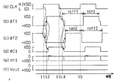
次に、このように構成される本実施の形態のチャージポンプ回路による負電圧の発生動作の概要を図2のタイミングチャートを参照して説明する。なお、同図2においては本チャージポンプ回路の定常的な推移が示され、電源投入時等の過渡的な推移は割愛されている。
【0028】
同図2に示す時刻t1においてクロック信号CLKが論理「H」レベル(VDD)に変化すると(図2(a))、まず上記インバータ12の出力が論理「L」レベル(0ボルト)となり、それに伴ってNAND回路15の出力が論理「H」レベルとなる。それがCMOSインバータ2に入力され、同インバータ2の出力である制御クロック信号φT2が論理「L」レベル「−VDD」となる(図2(c)参照)。
【0029】
このとき、スイッチングトランジスタTR2はオフするとともに、インバータ11の出力が論理「H」レベルとなり、それに伴ってNAND回路14の出力が論理「L」レベル(0ボルト)となる。それがCMOSインバータ1に入力され、同図2に示す時刻t2において、同インバータ1の出力である制御クロック信号φT1が論理「H」レベル(VDD)となる(図2(b)参照)。続いてバッファ回路B1の遅延による所定時間後、キャパシタクロック信号φC1が論理「H」レベル(VDD)となる(図2(d)参照)。この上昇に伴なって、ノード電圧Vn1は「−VDD」から上昇し、その後ほぼ0ボルトとなる(図2(e)参照)。
【0030】
一方、時刻t3においてクロック信号CLKが論理「L」レベル(0ボルト)に変化すると、まず上記NAND回路14の出力が論理「H」レベルとなり、それがCMOSインバータ1に入力され、同図2に示す時刻t4において、同インバータ1の出力である制御クロック信号φT1が「L」レベル「−VDD」となる(図2(b)参照)。このとき、スイッチングトランジスタTR1はオフする。続いてバッファ回路B1の遅延による所定時間後、キャパシタクロック信号φC1が論理「L」レベル(0ボルト)となる(図2(d)参照)。また、このとき、インバータ13の出力が論理「H」レベル(VDD)となり、それに伴ってNAND回路15の出力が論理「L」レベル(0ボルト)となる。それがCMOSインバータ2に入力され、同インバータ2の出力である制御クロック信号φT2が論理「H」レベル(VDD)となる(図2(c)参照)。このときスイッチングトランジスタTR2はオンする。その後、時刻t5においてクロック信号CLKが再び論理「H」レベルに変化すると、上記時刻t1と同様な動作が行われる。
【0031】
本実施の形態のチャージポンプ回路においては、このような動作が繰り返されることによって、スイッチングトランジスタTR1,TR2のしきい電圧Vthの影響がなくなり、ほぼ理論値「−VDD」に近い出力電圧Voutが得られるようになる(図2(f)参照)。
【0032】
また、本実施の形態のチャージポンプ回路においては上述したように、スイッチングトランジスタTR1,TR2が同時にオンされることはない。すなわち、同図2に示されるように、スイッチングトランジスタTR1のオフ期間τoff1内においてスイッチングトランジスタTR2のオン期間τon2が設定され、一方スイッチングトランジスタTR2のオフ期間τoff2内においてスイッチングトランジスタTR1のオン期間τon1が設定される。そのため、効率よく所望の出力電圧Voutが得られるようになるとともに、スイッチングトランジスタTR1,TR2に大きな貫通電流が流れることも防止される。その結果、同トランジスタTR1,TR2の信頼性が向上し、チャージポンプ回路としての信頼性も向上することとなる。
【0033】
以上説明したように、本実施の形態のチャージポンプ回路によれば、以下のような効果を得ることができる。
(1)スイッチングトランジスタTR1のゲート電圧を先に確定してから同トランジスタTR1のソース電圧(ノードN1の電圧)Vn1を変化させるようにしている。そのため、スイッチングトランジスタTR1のスイッチング時における寄生トランジスタの影響、及びノード電圧Vn1の変動等が防止されるようになる。その結果、チャージポンプ回路としての動作がより確実になるとともに、その信頼性も向上するようになる。
【0034】
(2)CMOSインバータ1,2のNチャネル型MOSトランジスタのソース端子SをスイッチングトランジスタTR1,TR2のソース端子Sに接続する構成としている。そのため簡易な構成により、同トランジスタTR1,TR2のオフ動作の維持を確実とするゲート電圧(制御クロック信号φT1,φT2)を得ることができる。
【0035】
(3)タイミング調整回路10によって、スイッチングトランジスタTR1,TR2が同時にオンすることのない制御クロック信号φT1,φT2が形成される。そのため、同トランジスタTR1,TR2に大きな貫通電流の流れることが防止され、同トランジスタTR1,TR2の信頼性が向上するとともに、チャージポンプ回路としての消費電力を低減することができる。
【0036】
(4)電圧変換に際してスイッチングトランジスタTR1,TR2のしきい値電圧Vthの影響を受けない構成としたため、高い到達出力電圧値(絶対値)が得られる。
【0037】
(第2の実施の形態)
次に、本発明にかかるチャージポンプ回路の第2の実施の形態を、前記第1の実施の形態との相違点を中心に図3及び図4を参照して説明する。
【0038】
図3に示されるように、この第2の実施の形態のチャージポンプ回路においては、タイミング調整回路の構成が前記第1の実施の形態のタイミング調整回路10の構成と相違する。また、本実施の形態においては、スイッチングトランジスタを4個、キャパシタを3個備え、電源電圧VDDから出力電圧として負電圧「−3VDD」(理論値)を出力する。
【0039】
さて、本実施の形態のタイミング調整回路20は、3個のインバータ21,22,23、及び2個のNOR回路24,25を備えて構成される。先のタイミング調整回路10と同様に、互いに位相の反転したクロック信号が印加されるスイッチングトランジスタが同時に導通状態となることのないよう、それらクロック信号のタイミングを調整する。
【0040】
また、スイッチングトランジスタTR1,TR2,TR3に対してそれぞれCMOSインバータ1,2,3、バッファ回路B1,B2,B3、及びキャパシタC1,C2,C3がそれぞれ設けられている。また、スイッチングトランジスタTR4にはCMOSインバータ4が設けられている。そして、ここでは制御クロック信号φT1,φT3、制御クロック信号φT2,φT4、及びキャパシタクロック信号φC1,φC3は共通化されている。
【0041】
次に図4のタイミングチャートを参照して、このように構成される本実施の形態のチャージポンプ回路の動作の概要を説明する。
ここでも先の図2に示した場合と同様に、制御クロック信号φT1,φT3をバッファ回路B1,B3を介して遅延させてキャパシタクロック信号φC1,φC3が形成されている(図4(b),(d)参照)。また制御クロック信号φT2をバッファ回路B2を介して遅延させてキャパシタクロック信号φC2が形成されている(図4(c),(e)参照)。
【0042】
また、制御クロック信号φT1,φT3及び制御クロック信号φT2,φT4は、互いに一方の論理レベル「L」(トランジスタ「オフ」)期間内に他方の論理レベル「H」(トランジスタ「オン」)期間が来るように形成されている(図4(b),(c)参照)。すなわち、同図4に示されるように、スイッチングトランジスタTR2,TR4のオフ期間τoff2内においてスイッチングトランジスタTR1,TR3のオン期間τon1が設定され、一方スイッチングトランジスタTR1,TR3のオフ期間τoff1内においてスイッチングトランジスタTR2,TR4のオン期間τon2が設定される。
【0043】
図5に、本実施の形態のチャージポンプ回路がIC(集積回路)内に適用された例として、CCDドライバの構成を示す。同ドライバはフレームトランスファ型CCDを駆動するものである。詳しくは同CCDの撮像部に発生した電荷を蓄積部に一挙に転送する、いわゆる電荷の垂直転送駆動を実現するもので、1チップのIC(集積回路)として形成される。そして、同図5に示すように、負電圧発生用チャージポンプ回路31、高電圧発生用チャージポンプ回路32、及び垂直ドライブ回路33等を備えて構成される。なお、ポンピングキャパシタC1,C2,C3,出力キャパシタCout等は、当該ドライバに外付けされる。
【0044】
そしてここでは、本実施の形態のチャージポンプ回路31によって、理論値出力電圧Voutとしてほぼ−3VDDが得られ、同出力電圧Voutは高電圧発生用チャージポンプ回路32及び垂直ドライブ回路33に出力される。
【0045】
また、高電圧発生用チャージポンプ回路32は、例えば先の図1に示したような回路構成に基づき形成される。なお、同チャージポンプ回路32にあっては、前記スイッチングトランジスタTR1,TR2はPチャネル型MOSトランジスタにて構成されるとともに、同トランジスタTR1のドレイン端子は電源電圧VDDに接続される。また、前記CMOSインバータ1,2を構成するPチャネル型MOSトランジスタのソース(電源側端子)は電源電圧VDDに接続され、一方、そのNチャネル型MOSトランジスタのソースは上記ノードN1に接続される。また、クロック信号CLKは、上記チャージポンプ回路32の出力電圧Voutに基づきレベル変換される。
【0046】
このように構成される本実施の形態のチャージポンプ回路によっても、先の第1の実施の形態の回路と同様に、以下のような効果を得ることができる。
(1)スイッチングトランジスタTR1,TR2,TR3のゲート電圧を先に確定してから各トランジスタTR1,TR2,TR3のソース電圧(ノードN1,N2,N3の電圧)Vn1,Vn2,Vn3を変化させるようにしている。そのため、スイッチングトランジスタTR1,TR2,TR3のスイッチング時における寄生トランジスタの影響、及びノード電圧Vn1,Vn2,Vn3の変動等が防止されるようになる。その結果、チャージポンプ回路としての動作がより確実になるとともに、その信頼性も向上するようになる。
【0047】
(2)CMOSインバータ1,2,3,4のNチャネル型MOSトランジスタのソース端子SをスイッチングトランジスタTR1,TR2,TR3,TR4のソース端子Sに接続する構成としている。そのため簡易な構成により、それらトランジスタTR1,TR2,TR3,TR4のオフ動作の維持を確実とするゲート電圧(制御クロック信号φT1,φT2,φT3,φT4)を得ることができる。
【0048】
(3)タイミング調整回路20によって、スイッチングトランジスタTR1,TR2,TR3,TR4の各隣接するトランジスタが同時にオンすることのない制御クロック信号φT1,φT2,φT3,φT4が形成される。そのため、それらトランジスタTR1,TR2,TR3,TR4に大きな貫通電流の流れることが防止され、同トランジスタTR1,TR2,TR3,TR4の信頼性が向上するとともに、チャージポンプ回路としての消費電力を低減することができる。
【0049】
(4)電圧変換に際してスイッチングトランジスタTR1,TR2,TR3,TR4のしきい値電圧Vthの影響を受けない構成としたため、高い到達出力電圧値(絶対値)が得られる。
【0050】
(第3の実施の形態)
以下、本発明にかかるチャージポンプ回路の第3の実施の形態について、上記第1の実施の形態との相違点を中心に図6及び図7を参照して説明する。
【0051】
図1に示した第1の実施形態においては、スイッチングトランジスタTR1をオン・オフ制御させる制御クロック信号φ1を所定時間遅延させたキャパシタクロックCφ1を生成すべく、バッファ回路B1が設けられた。このように、バッファ回路B1を設けることで、スイッチングトランジスタTR1のゲート電圧を確定してから同トランジスタTR1のソース電圧(ノードN1の電圧)Vn1を変化させることができ、ひいては寄生トランジスタの影響等を防止することができるようになる。
【0052】
ただしこの場合、トランジスタTR1がオンしてからバッファ回路B1が論理「H」レベルの信号を出力するまでの期間において、バッファ回路B1内で無駄な電流が消費される懸念がある。すなわち、トランジスタTR1がオンして、そのドレイン及びソース間が導通されることで、GNDからノードN1へ電流が流れ、ノードN1の電位Vn1が上昇する。そして、これに伴ってバッファ回路B1の出力端子側の電位が変化する。しかし、この時点においては、例えばバッファ回路B1が2段のCMOSインバータで構成される場合、出力側のインバータ内のNチャネル型MOSトランジスタがオンしているために、このMOSトランジスタを介してキャパシタC1から同MOSトランジスタの論理「L」レベル側の給電端子(接地端子)に電流が流れるようになる。
【0053】
このように、バッファ回路B1内において、キャパシタC1への蓄電と関係のない電流が消費されると、チャージポンプ回路としてもその昇圧変換効率が低下する要因となる。特に、バッファ回路B1の出力がキャパシタC1への入力となる関係上、その出力側のMOSトランジスタの駆動電力が大きく設定されているために、上記消費される電力も大きなものとなり、チャージポンプ回路としてのこうした昇圧変換効率の低下が無視できないものとなる。
【0054】
そこで本実施の形態においては、前記制御クロック信号φT1を所定時間遅延させてキャパシタクロックφC1を生成するバッファ回路(遅延回路)を、次のように構成するようにしている。すなわち、上記制御クロック信号φT1が論理「H」レベルとなる以前は、キャパシタC1への給電ラインをハイインピーダンス状態としておき、同制御クロック信号φT1が論理「H」レベルとなった後に、このキャパシタC1への給電ラインの電位が論理「H」レベルになる構成としている。
【0055】
図6に、このように構成されたバッファ回路を備える本実施の形態にかかるチャージポンプ回路を示す。
図6に示されるように、この回路も、基本的には先の第1の実施の形態と同様に、2個のスイッチングトランジスタTR1、TR2と、キャパシタC1、出力キャパシタCout、及びトランジスタTR1やTR2へ供給するクロック信号を調整するタイミング調整回路100を備えて構成される。
【0056】
そして、本実施の形態においては、上記構成に加えて、第1の実施の形態におけるバッファ回路B1の代わりとしてバッファ回路(遅延回路)110を備えている。
【0057】
このバッファ回路110は、電源電圧「VDD」が印加される給電端子112と、同端子112及びキャパシタC1間の導通を制御するPチャネル型MOSトランジスタ111と、接地端子114と、同端子114及びキャパシタC1間の導通を制御するNチャネル型MOSトランジスタ113とを備えている。
【0058】
そしてバッファ回路110においては、上記トランジスタTR1がオンされてから、キャパシタC1に論理「H」レベルの信号が供給されるまでの期間における電力の浪費を抑制すべく、次のような手順で上記各トランジスタ111及び113の制御信号を生成する。すなわち、制御クロック信号φT1を論理「H」レベルにすべく指令信号がタイミング調整回路100から入力されると、この指令信号に基づいてまず、トランジスタ113をオフとする制御信号を生成する。そして、このトランジスタ113をオフとする制御信号に基づいて論理「H」レベルの制御クロック信号φT1を生成する。更に、生成された論理「H」レベルの制御クロック信号φT1に基づいて、トランジスタ111をオン状態とする制御信号を生成する。
【0059】
具体的には、図6に示されるように、バッファ回路110は、タイミング調整回路100から供給される制御クロック信号とトランジスタ111のゲート端子へ印加される制御信号S111との論理積信号を制御信号S113としてトランジスタ113のゲート端子に印加するAND回路115を備えている。また、同バッファ回路110は、タイミング調整回路100から供給される制御クロック信号とAND回路115の出力信号との論理和反転信号(NOR条件信号)を制御クロック信号φT1としてトランジスタTR1のゲート端子に印加するNOR回路116を備えている。更に、同バッファ回路110は、NOR回路116の出力信号の論理反転信号S111を上記制御信号S111としてトランジスタ111のゲート端子へ印加するインバータ117を備えている。
【0060】
上記態様にて構成されるバッファ回路110によれば、トランジスタTR1のゲートへ印加される制御クロック信号φT1が論理「H」レベルになる以前には、トランジスタ113がオフ状態に保たれてキャパシタC1への給電ラインがハイインピーダンスとされる。そして、同制御クロック信号φT1が論理「H」レベルになった後に、トランジスタ111がオン状態とされて、このキャパシタC1への給電ラインに論理「H」レベルの電圧が印加される。
【0061】
一方、タイミング調整回路100は、先の第1の実施の形態と同様、クロック信号CLKを入力し、同クロック信号CLKに基づいて、トランジスタTR1及びTR2が同時にオンすることのないように調整されたクロック信号を生成する。このような調整を行うべく、タイミング調整回路100は、クロック信号CLKの論理レベル変化に伴い、制御クロック信号φT2として論理「L」レベルの信号を出力する場合には、同制御クロック信号φT2に基づいて、バッファ回路110に論理「H」レベルの制御クロック信号φT1を生成するように指令する信号を生成する。更に、タイミング調整回路100は、論理「L」レベルの制御クロック信号φT1を生成するよう指令する信号をバッファ回路110に出力する場合には、この出力される信号に基づいて論理「H」レベルの制御クロック信号φT2を生成する。
【0062】
具体的には、これも図6に示されるように、タイミング調整回路100は、クロック信号CLKを反転させる第1のインバータ101、バッファ回路110内のトランジスタ113のゲート端子に印加される制御信号S113とこの第1のインバータ101の出力信号との論理積信号をトランジスタTR2のゲート端子へ印加するAND回路102とを備えている。更に、タイミング調整回路100は、上記トランジスタTR2のゲート端子に印加される論理積信号を反転させる第2のインバータ103,及びこの第2のインバータ103の出力信号とクロック信号CLKとの論理積反転信号を上述した制御クロック信号φT1の生成を指令する信号としてバッファ回路110へ出力するNAND回路を備えている。
【0063】
なお、図6においては便宜上、先の図1に例示したような、トランジスタTR1及びTR2のソースが負電圧となるときに、この電圧値を上記制御クロック信号φT1、φT2の論理「L」レベルの電圧値とする構成については図示しないこととした。これを実現するためには、例えばAND回路102及びNOR回路116の本来接地される側の給電端子を、これらトランジスタTR1及びTR2のソース端子に接続するなどすればよい。以下では、このように構成されていることを前提にその動作を説明する。
【0064】
次に、上記態様にて構成されるチャージポンプ回路の全体の動作について、図7のタイミングチャートを併せ参照して更に詳述する。
いま、図7に示す時刻t1において、クロック信号CLKが論理「H」レベル(VDD)に変化したとすると(図7(a))、まず、第1のインバータ101の出力が論理「L」レベルに変化するのに伴い、時刻t2において、AND回路102からトランジスタTR2のゲート端子へ印加される制御クロック信号φT2が論理「L」レベル(−VDD)となる(図7(c))。これにより、トランジスタTR2がオフ状態となる。
【0065】
一方、このAND回路102の出力は、第2のインバータ103によって反転され、論理「H」レベルのクロック信号CLKとともに、NAND回路104に入力されるようになる。これにより、NAND回路104では、論理「L」レベルの信号を、制御クロック信号φT1の生成を指令する信号としてバッファ回路110へ出力する。
【0066】
このNAND回路104から出力される論理「L」レベルの信号は、バッファ回路110においてAND回路115に入力され、図7に示す時刻t3において、このAND回路115から論理「L」レベルの信号が上記制御信号S113としてトランジスタ113のゲート端子に印加される(図7(e))。また、このAND回路115から出力される論理「L」レベルの信号は、上記タイミング調整回路100のNAND回路104からの出力信号とともに、NOR回路116に入力される。これにより、図7に示す時刻t4において、NOR回路116からトランジスタTR1のゲート端子へ論理「H」レベルの制御クロック信号φT1が出力される(図7(b))。そして、この論理「H」レベルの制御クロック信号φT1の印加によって、トランジスタTR1がオン状態となる。
【0067】
このように、トランジスタTR1のゲート端子へ論理「H」レベルの制御クロック信号φT1が供給される以前に、まずトランジス113がオフ状態へと制御されるために、トランジスタTR1のオンに起因するキャパシタC1の電位変化(図7(f))に伴って流れるキャパシタC1及び接地端子114間に不要な電流が流れてしまうことを防止することができる。
【0068】
また、上記NOR回路116の出力信号は、インバータ117で反転され、論理「L」レベルの信号が制御信号S111としてトランジスタ111のゲート端子へ印加されるため、図7に示す時刻t5において、トランジスタ111がオン状態となる(図7(d))。これにより、キャパシタC1に加えられる電圧の電位は、論理「H」レベルに固定され(図7(f))、また、時刻t4頃から上昇し始めたノードN1の電位は、グランドレベルに固定される(図7(g))。
【0069】
一方、図7に示す時刻t6において、クロック信号CLKが論理「L」レベル(0ボルト)に変化すると、まず、NAND回路104からバッファ回路110へ出力される信号が論理「H」レベルに変化する。これによりバッファ回路110においては、NOR回路116から出力される制御クロック信号φT1が論理「L」レベルとなり、トランジスタTR1がオフとなる(図7(b))。また、このNOR回路116の出力は、インバータ117を介して論理「H」レベルの制御信号S111としてトランジスタ111のゲート端子に加えられる(図7(d))。
【0070】
更に、このインバータ117の出力は、AND回路115に入力される。同AND回路115では、このインバータ117から出力される論理「H」レベルの信号と上述したNAND回路104から出力される論理「H」レベルの信号との論理積条件に基づき、論理「H」レベルの信号を出力する。そして、この論理「H」レベルの信号が制御信号S113として、トランジスタ113のゲートに印加される(図7(e))とともに、AND回路102に入力される。そして、このAND回路102では、この論理「H」レベルの制御信号S113と、クロック信号CLKがインバータ101を介して反転された論理「H」レベルの信号との論理積条件に基づいて、論理「H」レベルの制御クロック信号φT2を生成し、これをトランジスタTR2のゲート端子に印加する(図7(c))。これにより、トランジスタTR2がオンとなり、同トランジスタTR2を介してノード電圧Vn1が出力電圧Voutとして出力される。
【0071】
本実施の形態にかかるチャージポンプ回路においては、このような動作が繰り返されることで、昇圧効率を好適に維持している。
以上説明したように、本実施の形態によれば、第1の実施の形態の前記(1)〜(4)あるいはこれに準じた効果に加えて、以下の効果が得られるようになる。
【0072】
(5)バッファ回路110のトランジスタ113をオフ状態とした後、トランジスタTR1をオン状態とすることで、トランジスタTR1がオンされてからキャパシタクロック信号φC1が論理「H」レベルとなるまでの間に、キャパシタC1と接地端子114との間で電力が消費されることを的確に回避することができる。
【0073】
(6)トランジスタ113をオフ状態としてからトランジスタ111をオン状態とすることで、トランジスタ113及び111間での貫通電流が流れることも回避される。
【0074】
(7)トランジスタ111がオフ状態となってからトランジスタ113をオン状態とすることで、トランジスタ113及び111間での貫通電流が流れることも回避される。
【0075】
(第4の実施の形態)
以下、本発明にかかるチャージポンプ回路の第4の実施の形態について、先の第2及び第3の実施の形態との相違点を中心に図8及び図9を参照して説明する。
【0076】
本実施の形態にかかるチャージポンプ回路は、図8に示されるように、先の第2の実施形態と同様、4個のスイッチングトランジスタTR1〜TR4と、3個のキャパシタC1〜C3とを備え、電源電圧「VDD」から出力電圧として負電圧「−3VDD」(理論値)を出力する回路である。そして、これらトランジスタTR1〜TR4のうち、隣接したトランジスタが同時に導通状態となることがないように、タイミング調整回路200を備えている。
【0077】
更に、本実施の形態にかかるチャージポンプ回路は、前述した寄生トランジスタの影響を回避すべく、先の第2の実施の形態におけるバッファ回路B1〜B3の代わりに、バッファ回路210及び220を備えている。ここで、バッファ回路210は、制御クロック信号φT1及びφT3を生成するとともに、同信号を所定期間遅延させて、キャパシタクロック信号φC1及びφC3を出力する回路である。また、バッファ回路220は、制御クロック信号φT2及びφT4を生成するとともに、同信号を所定期間遅延させて、キャパシタクロックφC2及びφC4を出力する回路である。そして、これらバッファ回路210及び220は、先の第3の実施の形態のバッファ回路110と同様の機能を有して、キャパシタC1〜C3と接地との間で電力が消費されることを防止する。
【0078】
すなわち、これらバッファ回路210及び220では、タイミング調整回路200から供給される信号に基づき、スイッチングトランジスタ(TR1〜TR4)のゲートに論理「H」レベルの制御クロック信号を印加する場合に、まず、接地端子(214,224)及びキャパシタ(C1〜C3)間の導通制御を行うトランジスタ(213,223)をオフとする。そして、これらトランジスタ(213,223)をオフとする論理「L」レベルの制御信号(S213,S223)に基づいて、スイッチングトランジスタ(TR1〜TR4)のゲート端子に印加する論理「H」レベルの制御クロック信号(φT1〜φT4)を生成する。次に、この論理「H」レベルの制御クロック信号(φT1〜φT4)に基づいて電源電圧VDDが印加される給電端子(212,222)及びキャパシタ(C1〜C3)間の導通制御を行うトランジスタ(211,221)をオンとする。
【0079】
そして、こうした機能を得るために、バッファ回路210,220はそれぞれ、先の第3の実施形態と同様、AND回路(215,225)と、NOR回路(216,226)と、インバータ(217,227)とを備えて構成されている。
【0080】
一方、上記タイミング調整回路200は、スイッチングトランジスタTR1〜TR4の各々隣接するものが同時にオンすることのないようにタイミング調整された信号を上記各バッファ回路210,220に供給する回路である。すなわち、クロック信号CLKの変化に伴い、制御クロック信号φT1及びφT3が論理「L」レベルになる場合には、バッファ回路210によって生成される同信号φT1及びφT3に基づいて、論理「H」レベルの制御クロック信号φT2及びφT4を生成するように指令する信号をバッファ回路220に対して出力する。逆に、クロック信号CLKの変化に伴い、制御クロック信号φT2及びφT4が論理「L」レベルになる場合には、バッファ回路220によって生成される同信号φT2及びφT4に基づいて、論理「H」レベルの制御クロック信号φT1及びφT3を生成するように指令する信号をバッファ回路210に対して出力する。
【0081】
具体的には、図8に示されるように、タイミング調整回路200は、クロック信号CLKとバッファ回路220のトランジスタ223のゲート端子に印加される信号との論理積反転信号(NAND条件信号)をバッファ回路210に対して出力する第1のNAND回路202を備えている。また、タイミング調整回路200は、クロック信号CLKを反転させるインバータ201を介して加えられる信号とバッファ回路のトランジスタ213のゲートに印加される信号との論理積反転信号をバッファ回路220に対して出力する第2のNAND回路203を備えている。
【0082】
なお、本実施の形態においても、上記スイッチングトランジスタTR1〜TR4を確実にオフさせるために、先の第2の実施形態と同様、それらトランジスタTR1〜TR2のソースが負電圧となるときに、この電圧を上記制御クロック信号φT1〜φT4の論理「L」レベルの電圧値とする構成を採用しているが、図8でのこの具体構成についての図示は割愛した。
【0083】
図9に、本実施の形態にかかるチャージポンプ回路の動作を示す。
図9に示されるように、本実施の形態のチャージポンプ回路においても、基本的には先の第3の実施の形態と同様、スイッチングトランジスタ(TR1〜TR4)がオン状態となってからキャパシタクロック(φC1〜φT3)がオン状態となるまでの遅延期間にキャパシタ(C1〜C3)と接地端子(214,224)との間で電力が消費されることを回避することができる態様で、各種タイミング信号が生成されている。
【0084】
また、トランジスタ(211,221)がオフしてからトランジスタ(213,223)がオン状態となるため、これらトランジスタ間に貫通電流が流れることもなくなる。
【0085】
このため、この第4の実施の形態によっても、第2の実施形態による(1)〜(4)の効果に加えて、第3の実施の形態による前記(5)〜(7)の効果に準じた効果を得ることができるようになる。
【0086】
なお、上記第3及び第4の実施の形態は、以下のように変更して実施することもできる。
・バッファ回路110、210、220の構成は図6或いは図8に例示したものに限られない。特に、バッファ回路内のAND回路やNOR回路等の組み合わせについては、その変更も極めて容易である。すなわち、バッファ回路内に一対の論理回路を備え、、その一方の論理回路が、他方の出力とバッファ回路への入力信号とを合成して、一対の電源端子間に接続される一対のトランジスタが同時に非導通状態となる期間を設定し、同期間の後にキャパシタに所定の電位を与えるものを極めて容易に構成することができる。
【0087】
また、ここでは上記各実施の形態において例示された、低電位の給電端子及びキャパシタ間を遮断させる制御信号に基づいてトランジスタを導通制御する活性信号を生成したり、同活性信号に基づいて高電位の給電端子及びキャパシタ間を導通させる制御信号を生成する構成にも限られない。例えば、配線遅延を利用するなどしてもよい。
【0088】
その他、上記全ての実施の形態に共通に変更可能な要素としては次のようなものがある。
・タイミング調整回路の回路構成は、先の図1及び図3及び図6及び図8に示したタイミング調整回路10,20,100,200の構成に限られるものではない。要は、タイミング調整回路として、互いに位相の反転したクロック信号が印加されるスイッチングトランジスタが同時に導通状態となることのないよう、それらクロック信号のタイミングを調整するものであれば、いかなる回路構成にて構成されるものであってもよい。
【0089】
・スイッチングトランジスタとしてNチャネル型MOSトランジスタを使用する例を示したがこれに限られず、同スイッチングトランジスタとしてはその他、例えばPチャネル型MOSトランジスタを使用しても、あるいはNチャネル及びPチャネル型MOSトランジスタを併用しても、本発明のチャージポンプ回路を構成することはできる。
【0090】
・また、本発明のチャージポンプ回路は、電源電圧VDDを降圧して負電圧を発生させる適用例に限られず、その他、例えば電源電圧VDDを昇圧したり、あるいは負電圧を利用して正電圧を発生させたりする等、様々な電圧変換の態様に適用することができる。
【0091】
・また、スイッチングトランジスタの個数、同トランジスタ間にその一方の電極が接続されてキャパシタ(ポンピングキャパシタ)の個数は任意であり、それぞれ所望の出力電圧Voutを得るに必要な個数を適宜設けるようにすればよい。
【0092】
・また、上記各実施の形態では便宜上、スイッチングトランジスタTR1,TR2,TR3,TR4のソースS及びドレインDについてこれを図1あるいは図3のごとく定めたが、これらの態様に固定されるものではない。
【0093】
・更に、上記第1又は第2の実施形態におけるバッファ回路B1〜B3や、第3及び第4の実施形態におけるバッファ回路110,210,220においては、キャパシタへの給電を行う給電端子を、電位「VDD」、「0」を有するものにそれぞれ設定したが、これに限定されるものでもない。要は、スイッチングトランジスタの導通制御端子に印加されるクロック信号の2値的な値に対応した異なる2つの電位に設定されるものであればよい。そして、これら電位を適宜変更することで、チャージポンプ回路としての昇圧能力を調整することもできる。
【0094】
【発明の効果】
請求項1記載の発明によれば、遅延回路(バッファ回路)により、先にスイッチングトランジスタの例えばゲート端子(導通制御端子)に電圧を印加してから同トランジスタのソース電圧(ノードの電圧)を変化させることができる。そのため、スイッチングトランジスタのスイッチング時における寄生トランジスタ(当該トランジスタの半導体基板内に擬似形成されるトランジスタ)の影響、及びノード電圧の変動等が防止されるようになる。その結果、チャージポンプ回路としての動作がより確実になるとともに、その信頼性も向上するようになる。
【0095】
請求項2記載の発明によれば、所定の電源電位と前記のノード電位との間で動作するバッファ回路を設けることにより、簡易な構成により、前記スイッチングトランジスタのオフ動作の維持を確実とする同トランジスタのゲート電圧(導通制御端子印加クロック信号)を得ることができる。
【0096】
請求項3記載の発明によれば、タイミング調整回路によって、複数のトランジスタの奇数段と偶数段とが同時に非導通状態となる期間を設けるクロック信号が形成される。そのため、それらトランジスタに大きな貫通電流の流れることが防止され、同トランジスタの信頼性が向上するとともに、チャージポンプ回路としての消費電力を低減することができる。
【0097】
請求項4または5記載の発明によれば、前記タイミング調整回路を簡易な回路構成にて好適に形成することができる。
請求項6記載の発明によれば、キャパシタの他方の端子を開放して一旦ハイインピーダンス状態とすることで、トランジスタが導通制御されるのに伴いキャパシタの他方の端子側の線路の電位が上昇したとしても、この遅延回路内で電力が消費されることを回避することができるようになる。更に、同発明によれば、トランジスタに印加されるクロック信号が反転した後に、キャパシタの他方の端子に所定の電位を与えることで、寄生トランジスタ効果等を回避することができるようになる。
【0098】
請求項7及び8記載の発明によれば、請求項6記載の遅延回路を簡易な回路構成にて好適に形成することができる。
【図面の簡単な説明】
【図1】本発明にかかるチャージポンプ回路についてその第1の実施の形態を示す回路図。
【図2】同実施の形態の回路の動作を示すタイミングチャート。
【図3】本発明にかかるチャージポンプ回路についてその第2の実施の形態を示す回路図。
【図4】同実施の形態の回路の動作を示すタイミングチャート。
【図5】同実施の形態の回路の適用例を示すブロック図。
【図6】本発明にかかるチャージポンプ回路についてその第3の実施の形態を示す回路図。
【図7】同実施の形態の回路の動作を示すタイミングチャート。
【図8】本発明にかかるチャージポンプ回路についてその第4の実施の形態を示す回路図。
【図9】同実施の形態の回路の動作を示すタイミングチャート。
【図10】従来のチャージポンプ回路の構成例を示す回路図。
【図11】同従来のチャージポンプ回路の動作を示すタイミングチャート。
【符号の説明】
1,2,3,4…CMOSインバータ、1a,2a…Nチャネル型MOSトランジスタ、10,20,100,200…タイミング調整回路、B1,B2,B3,B4…バッファ回路、C1,C2,C3,C4…キャパシタ、TR1,TR2,TR3,TR4…スイッチングトランジスタ、110,210,220…遅延回路。[0001]
BACKGROUND OF THE INVENTION
The present invention relates to a charge pump circuit that converts a voltage using a capacitor.
[0002]
[Prior art]
FIG. 10 shows an outline of the configuration of a conventional charge pump circuit. Here, the circuit shown in FIG. 10A includes two diodes D1 and D2, a capacitor C1, an output capacitor Cout, and the like. FIG. 10B shows an example in which the diodes D1 and D2 are configured by P-channel MOS transistors T1 and T2.
[0003]
All of these charge pump circuits are supplied with the clock signal CLK to the node N1 through the capacitor C1, and thereby output voltage based on the power supply voltage VDD which is the logic “H (high)” level value of the clock signal CLK. This is a charge pump circuit that outputs a negative voltage “−VDD” as Vout (steps up to the negative side).
[0004]
Next, the outline of the voltage conversion operation of the circuit will be described with reference to FIG.
In the state where the clock signal CLK before time t1 shown in FIG. 11 is at the logic “H” level, the diode D1 (or transistor TR1) is turned on and the voltage Vn1 at the node N1 is almost “0” volts (ground voltage GND). ).
At this time, the output voltage Vout is also assumed to be substantially the ground voltage GND.
[0005]
When the clock signal CLK falls to the logic “L (low)” level (0 volt) at time t1 shown in FIG. 1, the node voltage Vn1 is pulled to almost “−VDD” by the capacitor C1. At this time, since the diode D1 (transistor TR1) is turned off and the diode D2 (transistor TR2) is turned on, the output voltage Vout is substantially “−VDD” (see FIG. 11C), and the output capacitor Cout is “−VDD”. Will be charged.
[0006]
Subsequently, when the clock signal CLK again becomes the logic “H” level at time t2, the node voltage Vn1 is substantially raised to the ground voltage GND by the capacitor C1. Therefore, the diode D2 (transistor TR2) is turned off, and the output voltage Vout is held near the charging voltage “−VDD” of the output capacitor Cout.
[0007]
Next, when the clock signal CLK again becomes the logic “L” level at time t3, the node voltage Vn1 is again pulled to substantially “−VDD”. At this time, since the diode D1 (transistor TR1) is turned off and the diode D2 (transistor TR2) is turned on, the output voltage Vout becomes “−VDD” again, and the output capacitor Cout is charged to −VDD. By repeating such charging of the output capacitor Cout, the output voltage Vout is maintained at approximately “−VDD”.
[0008]
Since such a charge pump circuit can be integrated into an IC (integrated circuit) by simply attaching capacitors C1 and Cout, as a voltage conversion means for obtaining a desired voltage value in the IC, for example, a CCD ( It is used for a power supply circuit of a driver, a memory IC, etc.
[0009]
[Problems to be solved by the invention]
By the way, in such a charge pump circuit, voltage conversion can be performed with a simple configuration, that is, although the voltage can be increased or decreased, the diodes D1, D2 (or transistors T1, T2) Due to the influence of the voltage drop due to the threshold voltage Vth, there arises a disadvantage that the absolute value of the output voltage decreases. For example, in the conventional charge pump circuit, the theoretical value of the absolute value of the output voltage is (VDD−2Vth), which is lower than the maximum theoretical value VDD by 2Vth. Such a decrease in the absolute value of the output voltage leads to a decrease in voltage conversion efficiency as a charge pump circuit.
[0010]
In order to avoid a decrease in output voltage (absolute value) due to the threshold voltage Vth, for example, the P-channel MOS transistors T1 and T2 shown in FIG. However, in that case, a decrease in voltage conversion efficiency due to a through current or the like during on / off control of the transistors and a decrease in reliability of the transistors cannot be ignored.
[0011]
The present invention has been made in view of the above circumstances, and an object of the present invention is to provide a charge pump circuit capable of improving its voltage conversion efficiency while maintaining high reliability.
[0012]
[Means for Solving the Problems]
In the following, means for achieving the above object and its effects are described.
According to the first aspect of the present invention, one terminal is connected to a plurality of switching transistors connected in series between the output terminal and the reference potential terminal, and a node between adjacent transistors. A capacitor having the other terminal connected to the conduction control terminal of the transistor on the reference potential end side, and the phases of the conduction control terminals of the plurality of transistors are inverted at odd and even stages. In a charge pump circuit that applies a clock signal to generate a predetermined output potential at the output terminal, a delay circuit is provided between the other terminal of the capacitor and a transistor conduction control terminal connected thereto, The clock signal applied to the conduction control terminal is delayed for a predetermined period and applied to the other terminal of the capacitor. And the gist thereof.
[0013]
According to a second aspect of the present invention, in the charge pump circuit according to the first aspect, the clock signal is connected to a conduction control terminal of the switching transistor via a buffer circuit that operates between a predetermined power supply potential and the potential of the node. The gist is to be applied to.
[0014]
According to a third aspect of the present invention, in the charge pump circuit according to the first or second aspect, the phases of the plurality of switching transistors are set so as to set a period in which the odd-numbered stages and the even-numbered stages of the plurality of switching transistors are simultaneously non-conductive. The gist of the invention is to further include a timing adjustment circuit for adjusting the timing of the inverted clock signal.
[0015]
According to a fourth aspect of the present invention, in the charge pump circuit according to the third aspect, the timing adjusting circuit receives a clock signal applied to a conduction control terminal of one of the adjacent transistors and inverts its phase. A first NAND circuit, a first NAND circuit that receives a clock signal input to the charge pump circuit and an output clock signal of the first inverter circuit and takes the NAND condition thereof, and the charge pump circuit A second inverter circuit for inverting the input clock signal, a third inverter circuit for receiving the clock signal applied to the conduction control terminal of the other transistor of the adjacent transistor and inverting the phase thereof, The output clock signals of the second and third inverter circuits are input to satisfy the NAND condition. Of a NAND circuit, and its gist that the adjusted clock signal of the timing with a output of the first and second NAND circuits.
[0016]
According to a fifth aspect of the present invention, in the charge pump circuit according to the third aspect, the timing adjustment circuit includes a first inverter circuit that inverts a clock signal input to the charge pump circuit, and one of the adjacent transistors. A first NOR circuit that takes a NOR condition by inputting a clock signal applied to a conduction control terminal of the transistor and an output clock signal of the first inverter circuit, and an output clock signal of the first NOR circuit A second inverter circuit for inverting the clock signal, a clock signal input to the charge pump circuit, and a clock signal applied to the conduction control terminal of the other transistor of the adjacent transistor are input to satisfy the NOR condition. 2 NOR circuit and a third inverter circuit for inverting the output clock signal of the second NOR circuit The equipped, as its gist to the adjusted clock signal of the timing with a output of the second and third inverter circuit.
[0017]
According to a sixth aspect of the present invention, in the charge pump circuit according to any one of the first to third aspects, the delay circuit opens the other terminal of the capacitor to once enter a high impedance state, and The gist is that a predetermined potential is applied to the other terminal of the capacitor after a predetermined delay period after the clock signal applied to the conduction control terminal is inverted.
[0018]
According to a seventh aspect of the present invention, in the charge pump circuit according to the sixth aspect, the delay circuit drives a pair of transistors connected in series between a pair of power supply terminals and a conduction control terminal of the pair of transistors. A pair of logic circuits, wherein one of the pair of logic circuits combines the output of the other and the clock signal to set a period in which the pair of transistors are in a non-conducting state at the same time, and the pair of transistors The gist thereof is to apply a potential between the capacitor to the capacitor.
[0019]
According to an eighth aspect of the present invention, in the charge pump circuit according to the seventh aspect, the pair of transistors includes a P-channel transistor that controls conduction between a high-potential side power supply terminal and the capacitor, and a low-potential side And the pair of logic circuits are composed of AND circuits and NOR circuits, and the AND circuit includes an input clock signal and the P signal. A logical product signal with a signal applied to the conduction control terminal of the channel type transistor is applied to the conduction control terminal of the N channel type transistor, and the NOR circuit includes the clock signal inputted to the delay circuit and the AND circuit. Applying a NOR condition signal with the output signal to the conduction control terminal of the switching transistor, the output of the NOR circuit That signal is inverted is applied to the conduction control terminal of the P-channel transistor and its gist.
[0020]
DETAILED DESCRIPTION OF THE INVENTION
(First embodiment)
A first embodiment of a charge pump circuit according to the present invention will be described below with reference to FIGS. The charge pump circuit according to the present embodiment is also a charge pump circuit that outputs a negative voltage “−VDD” as an output voltage from the power supply voltage VDD.
[0021]
FIG. 1 shows a configuration of a charge pump circuit according to the present embodiment. As shown in FIG. 1, this circuit is basically composed of two charge pump circuits as in the prior art charge pump circuit. The switching transistors TR1 and TR2, the capacitor C1, and the output capacitor Cout are configured. Here, the transistors TR1 and TR2 are composed of N-channel MOS transistors here.
In addition to these basic configurations as a charge pump circuit, the charge pump circuit of the present embodiment further includes a timing adjustment circuit 10,
[0022]
Here, the timing adjustment circuit 10 includes
[0023]
In the
[0024]
The buffer circuit B1 is provided between the output of the
[0025]
As described above, in the present embodiment, by generating the capacitor clock signal φC1, by applying the on / off signal to the gate of the switching transistor TR1, the capacitor clock signal φC1 is applied to the capacitor C1. The source voltage (voltage at the node N1) Vn1 of the transistor TR1 is changed.
[0026]
Therefore, when the switching transistor TR1 is turned on, problems such as conduction of a parasitic transistor formed in the semiconductor substrate of the transistor TR1 are prevented. On the other hand, when the transistor TR1 is turned off, the transistor TR1 is turned off. Thus, the node voltage Vn1 is also prevented from changing.
[0027]
Next, the outline of the negative voltage generating operation by the charge pump circuit of the present embodiment configured as described above will be described with reference to the timing chart of FIG. In FIG. 2, a steady transition of the charge pump circuit is shown, and a transitional transition such as when the power is turned on is omitted.
[0028]
When the clock signal CLK changes to the logic “H” level (VDD) at time t1 shown in FIG. 2 (FIG. 2A), the output of the
[0029]
At this time, the switching transistor TR2 is turned off, and the output of the inverter 11 becomes the logic “H” level, and accordingly, the output of the
[0030]
On the other hand, when the clock signal CLK changes to the logic “L” level (0 volt) at time t3, the output of the
[0031]
In the charge pump circuit of the present embodiment, by repeating such an operation, the influence of the threshold voltage Vth of the switching transistors TR1 and TR2 is eliminated, and an output voltage Vout that is substantially close to the theoretical value “−VDD” is obtained. (See FIG. 2 (f)).
[0032]
In the charge pump circuit of the present embodiment, as described above, the switching transistors TR1 and TR2 are not simultaneously turned on. That is, as shown in FIG. 2, the on period τon2 of the switching transistor TR2 is set within the off period τoff1 of the switching transistor TR1, while the on period τon1 of the switching transistor TR1 is set within the off period τoff2 of the switching transistor TR2. Is done. Therefore, a desired output voltage Vout can be obtained efficiently, and a large through current is prevented from flowing through the switching transistors TR1 and TR2. As a result, the reliability of the transistors TR1 and TR2 is improved, and the reliability as a charge pump circuit is also improved.
[0033]
As described above, according to the charge pump circuit of the present embodiment, the following effects can be obtained.
(1) After determining the gate voltage of the switching transistor TR1 first, the source voltage (voltage of the node N1) Vn1 of the transistor TR1 is changed. Therefore, the influence of the parasitic transistor at the time of switching of the switching transistor TR1, the fluctuation of the node voltage Vn1, and the like are prevented. As a result, the operation as a charge pump circuit becomes more reliable and the reliability thereof is improved.
[0034]
(2) The source terminals S of the N-channel MOS transistors of the
[0035]
(3) The timing adjustment circuit 10 generates control clock signals φT1 and φT2 in which the switching transistors TR1 and TR2 are not simultaneously turned on. Therefore, it is possible to prevent a large through current from flowing through the transistors TR1 and TR2, thereby improving the reliability of the transistors TR1 and TR2, and reducing the power consumption of the charge pump circuit.
[0036]
(4) Since the configuration is not affected by the threshold voltage Vth of the switching transistors TR1 and TR2 during voltage conversion, a high ultimate output voltage value (absolute value) can be obtained.
[0037]
(Second Embodiment)
Next, a second embodiment of the charge pump circuit according to the present invention will be described with reference to FIGS. 3 and 4 with a focus on differences from the first embodiment.
[0038]
As shown in FIG. 3, in the charge pump circuit of the second embodiment, the configuration of the timing adjustment circuit is different from the configuration of the timing adjustment circuit 10 of the first embodiment. In the present embodiment, four switching transistors and three capacitors are provided, and a negative voltage “−3 VDD” (theoretical value) is output as an output voltage from the power supply voltage VDD.
[0039]
The
[0040]
Also,
[0041]
Next, the outline of the operation of the charge pump circuit of the present embodiment configured as described above will be described with reference to the timing chart of FIG.
Here, similarly to the case shown in FIG. 2, the control clock signals φT1 and φT3 are delayed through the buffer circuits B1 and B3 to form the capacitor clock signals φC1 and φC3 (FIG. 4B, (See (d)). Further, the control clock signal φT2 is delayed through the buffer circuit B2 to form the capacitor clock signal φC2 (see FIGS. 4C and 4E).
[0042]
The control clock signals φT1 and φT3 and the control clock signals φT2 and φT4 have the other logic level “H” (transistor “on”) period within one logic level “L” (transistor “off”) period. (See FIGS. 4B and 4C). That is, as shown in FIG. 4, the ON period τon1 of the switching transistors TR1 and TR3 is set within the OFF period τoff2 of the switching transistors TR2 and TR4, while the switching transistor TR2 is set within the OFF period τoff1 of the switching transistors TR1 and TR3. , TR4 ON period τon2 is set.
[0043]
FIG. 5 shows the configuration of a CCD driver as an example in which the charge pump circuit of this embodiment is applied to an IC (integrated circuit). The driver drives a frame transfer type CCD. Specifically, it realizes so-called vertical transfer driving of charges, in which charges generated in the image pickup unit of the CCD are transferred to the storage unit at once, and is formed as a one-chip IC (integrated circuit). As shown in FIG. 5, a negative voltage generating
[0044]
Here, the
[0045]
Further, the high-voltage generating
[0046]
Also by the charge pump circuit of this embodiment configured as described above, the following effects can be obtained in the same manner as the circuit of the first embodiment.
(1) The gate voltages of the switching transistors TR1, TR2, and TR3 are determined first, and then the source voltages (voltages of the nodes N1, N2, and N3) Vn1, Vn2, and Vn3 of the transistors TR1, TR2, and TR3 are changed. ing. For this reason, the influence of parasitic transistors at the time of switching of the switching transistors TR1, TR2, and TR3, fluctuations in the node voltages Vn1, Vn2, and Vn3, and the like are prevented. As a result, the operation as a charge pump circuit becomes more reliable and the reliability thereof is improved.
[0047]
(2) The source terminals S of the N-channel MOS transistors of the
[0048]
(3) The
[0049]
(4) Since the configuration is not affected by the threshold voltage Vth of the switching transistors TR1, TR2, TR3, and TR4 during voltage conversion, a high ultimate output voltage value (absolute value) can be obtained.
[0050]
(Third embodiment)
Hereinafter, a third embodiment of the charge pump circuit according to the present invention will be described with reference to FIGS. 6 and 7, focusing on differences from the first embodiment.
[0051]
In the first embodiment shown in FIG. 1, the buffer circuit B1 is provided to generate the capacitor clock Cφ1 obtained by delaying the control clock signal φ1 for controlling the on / off of the switching transistor TR1 for a predetermined time. As described above, by providing the buffer circuit B1, the source voltage (voltage of the node N1) Vn1 of the transistor TR1 can be changed after the gate voltage of the switching transistor TR1 is determined. Can be prevented.
[0052]
However, in this case, there is a concern that useless current is consumed in the buffer circuit B1 during a period from when the transistor TR1 is turned on until the buffer circuit B1 outputs a logic “H” level signal. That is, when the transistor TR1 is turned on and the drain and source thereof are conducted, a current flows from GND to the node N1, and the potential Vn1 of the node N1 rises. Along with this, the potential on the output terminal side of the buffer circuit B1 changes. However, at this time, for example, when the buffer circuit B1 is formed of a two-stage CMOS inverter, the N-channel MOS transistor in the inverter on the output side is turned on, so that the capacitor C1 is connected via this MOS transistor. Current flows from the power supply terminal (ground terminal) on the logic “L” level side of the MOS transistor.
[0053]
As described above, when a current unrelated to the power storage in the capacitor C1 is consumed in the buffer circuit B1, the boost conversion efficiency of the charge pump circuit is reduced. In particular, since the output of the buffer circuit B1 becomes an input to the capacitor C1, since the driving power of the MOS transistor on the output side is set large, the consumed power becomes large, and the charge pump circuit Such a decrease in boost conversion efficiency cannot be ignored.
[0054]
Therefore, in the present embodiment, a buffer circuit (delay circuit) that generates the capacitor clock φC1 by delaying the control clock signal φT1 for a predetermined time is configured as follows. That is, before the control clock signal φT1 becomes the logic “H” level, the power supply line to the capacitor C1 is set in the high impedance state, and after the control clock signal φT1 becomes the logic “H” level, the capacitor C1 In this configuration, the potential of the power supply line is set to a logic “H” level.
[0055]
FIG. 6 shows a charge pump circuit according to the present embodiment including the buffer circuit configured as described above.
As shown in FIG. 6, this circuit also basically has two switching transistors TR1 and TR2, a capacitor C1, an output capacitor Cout, and transistors TR1 and TR2 as in the first embodiment. And a
[0056]
In this embodiment, in addition to the above configuration, a buffer circuit (delay circuit) 110 is provided instead of the buffer circuit B1 in the first embodiment.
[0057]
The
[0058]
In the
[0059]
Specifically, as shown in FIG. 6, the
[0060]
According to the
[0061]
On the other hand, the
[0062]
Specifically, as also shown in FIG. 6, the
[0063]
In FIG. 6, for the sake of convenience, when the sources of the transistors TR1 and TR2 have a negative voltage as illustrated in FIG. 1, the voltage value is set to the logic “L” level of the control clock signals φT1 and φT2. The configuration for the voltage value is not shown. To achieve this, for example, an AND
[0064]
Next, the overall operation of the charge pump circuit configured as described above will be described in more detail with reference to the timing chart of FIG.
If the clock signal CLK changes to the logic “H” level (VDD) at time t1 shown in FIG. 7 (FIG. 7A), the output of the first inverter 101 is first set to the logic “L” level. Accordingly, at time t2, the control clock signal φT2 applied from the AND
[0065]
On the other hand, the output of the AND
[0066]
The logic “L” level signal output from the
[0067]
Thus, before the control clock signal φT1 having the logic “H” level is supplied to the gate terminal of the transistor TR1, the
[0068]
Further, the output signal of the NOR
[0069]
On the other hand, when clock signal CLK changes to logic “L” level (0 volts) at time t6 shown in FIG. 7, first, the signal output from
[0070]
Further, the output of the
[0071]
In the charge pump circuit according to the present embodiment, such an operation is repeated, so that the boosting efficiency is suitably maintained.
As described above, according to the present embodiment, the following effects can be obtained in addition to the effects (1) to (4) of the first embodiment or effects equivalent thereto.
[0072]
(5) By turning off the
[0073]
(6) By turning on the transistor 111 after the
[0074]
(7) By turning on the
[0075]
(Fourth embodiment)
Hereinafter, a fourth embodiment of the charge pump circuit according to the present invention will be described with reference to FIGS. 8 and 9, focusing on the differences from the second and third embodiments.
[0076]
As shown in FIG. 8, the charge pump circuit according to the present embodiment includes four switching transistors TR1 to TR4 and three capacitors C1 to C3, as in the second embodiment. This circuit outputs a negative voltage “−3 VDD” (theoretical value) as an output voltage from the power supply voltage “VDD”. The
[0077]
Furthermore, the charge pump circuit according to the present embodiment includes
[0078]
That is, in the
[0079]
In order to obtain such a function, the
[0080]
On the other hand, the
[0081]
Specifically, as shown in FIG. 8, the
[0082]
Also in this embodiment, in order to surely turn off the switching transistors TR1 to TR4, as in the second embodiment, when the sources of the transistors TR1 to TR2 become negative voltages, Is adopted as the voltage value of the logic “L” level of the control clock signals φT1 to φT4, but the illustration of this specific configuration in FIG. 8 is omitted.
[0083]
FIG. 9 shows the operation of the charge pump circuit according to this embodiment.
As shown in FIG. 9, in the charge pump circuit according to the present embodiment as well, basically, as in the third embodiment, the capacitor clock is turned on after the switching transistors (TR1 to TR4) are turned on. Various timings are provided in such a manner that it is possible to avoid power consumption between the capacitors (C1 to C3) and the ground terminals (214, 224) during a delay period until the (φC1 to φT3) is turned on. A signal is being generated.
[0084]
Further, since the transistors (213, 223) are turned on after the transistors (211, 221) are turned off, no through current flows between these transistors.
[0085]
For this reason, also in the fourth embodiment, in addition to the effects (1) to (4) according to the second embodiment, the effects (5) to (7) according to the third embodiment are achieved. A similar effect can be obtained.
[0086]
Note that the third and fourth embodiments can be implemented with the following modifications.
The configuration of the
[0087]
In addition, here, an active signal for controlling conduction of a transistor is generated based on a control signal for cutting off between a low-potential power supply terminal and a capacitor exemplified in the above embodiments, and a high potential is generated based on the active signal. It is not restricted to the structure which produces | generates the control signal which conducts between the electric power feeding terminal and capacitor. For example, wiring delay may be used.
[0088]
Other elements that can be commonly changed in all the above-described embodiments include the following.
The circuit configuration of the timing adjustment circuit is not limited to the configuration of the
[0089]
An example in which an N-channel MOS transistor is used as a switching transistor has been shown, but the present invention is not limited to this. Even in combination, the charge pump circuit of the present invention can be configured.
[0090]
In addition, the charge pump circuit of the present invention is not limited to an application example in which the power supply voltage VDD is stepped down to generate a negative voltage. For example, the power supply voltage VDD is stepped up, or the positive voltage is increased using the negative voltage. It can be applied to various modes of voltage conversion such as generation.
[0091]
The number of switching transistors and the number of capacitors (pumping capacitors) are arbitrary as one electrode is connected between the transistors, and the number necessary to obtain a desired output voltage Vout is appropriately provided. That's fine.
[0092]
In the above embodiments, for convenience, the sources S and drains D of the switching transistors TR1, TR2, TR3, and TR4 are determined as shown in FIG. 1 or FIG. 3, but are not fixed to these modes. .
[0093]
Furthermore, in the buffer circuits B1 to B3 in the first or second embodiment and the
[0094]
【The invention's effect】
According to the first aspect of the present invention, after the voltage is first applied to, for example, the gate terminal (conduction control terminal) of the switching transistor by the delay circuit (buffer circuit), the source voltage (node voltage) of the transistor is changed. Can be made. Therefore, the influence of the parasitic transistor (transistor formed in the semiconductor substrate of the transistor) at the time of switching of the switching transistor, fluctuation of the node voltage, and the like are prevented. As a result, the operation as a charge pump circuit becomes more reliable and the reliability thereof is improved.
[0095]
According to the second aspect of the present invention, by providing a buffer circuit that operates between a predetermined power supply potential and the node potential, it is possible to reliably maintain the OFF operation of the switching transistor with a simple configuration. The gate voltage (conduction control terminal application clock signal) of the transistor can be obtained.
[0096]
According to the third aspect of the present invention, the timing adjustment circuit generates a clock signal that provides a period in which the odd-numbered stages and the even-numbered stages of the plurality of transistors are simultaneously turned off. Therefore, it is possible to prevent a large through current from flowing through these transistors, improving the reliability of the transistors and reducing the power consumption of the charge pump circuit.
[0097]
According to the invention of
According to the sixth aspect of the invention, the potential of the line on the other terminal side of the capacitor increases as the transistor is controlled to conduct by opening the other terminal of the capacitor to once enter a high impedance state. However, it is possible to avoid power consumption in the delay circuit. Furthermore, according to the present invention, after a clock signal applied to the transistor is inverted, a predetermined potential is applied to the other terminal of the capacitor, thereby making it possible to avoid a parasitic transistor effect or the like.
[0098]
According to the seventh and eighth aspects of the invention, the delay circuit of the sixth aspect can be suitably formed with a simple circuit configuration.
[Brief description of the drawings]
FIG. 1 is a circuit diagram showing a first embodiment of a charge pump circuit according to the present invention.
FIG. 2 is a timing chart showing the operation of the circuit of the embodiment.
FIG. 3 is a circuit diagram showing a second embodiment of the charge pump circuit according to the present invention.
FIG. 4 is a timing chart showing the operation of the circuit of the embodiment.
FIG. 5 is an exemplary block diagram showing an application example of the circuit of the embodiment;
FIG. 6 is a circuit diagram showing a third embodiment of the charge pump circuit according to the present invention.
FIG. 7 is a timing chart showing the operation of the circuit of the embodiment.
FIG. 8 is a circuit diagram showing a fourth embodiment of the charge pump circuit according to the present invention.
FIG. 9 is a timing chart showing the operation of the circuit of the embodiment;
FIG. 10 is a circuit diagram showing a configuration example of a conventional charge pump circuit.
FIG. 11 is a timing chart showing the operation of the conventional charge pump circuit.
[Explanation of symbols]
1, 2, 3, 4 ... CMOS inverter, 1a, 2a ... N-channel MOS transistor, 10, 20, 100, 200 ... Timing adjustment circuit, B1, B2, B3, B4 ... Buffer circuit, C1, C2, C3 C4: capacitor, TR1, TR2, TR3, TR4 ... switching transistor, 110, 210, 220 ... delay circuit.
Claims (8)
前記キャパシタの他方の端子とこれに接続されるトランジスタ導通制御端子との間に遅延回路を設け、当該トランジスタの導通制御端子に印加されるクロック信号を所定期間遅延させて前記キャパシタの他方の端子に印加するようにした
ことを特徴とするチャージポンプ回路。One terminal is connected to a plurality of switching transistors connected in series between the output terminal and the reference potential terminal, and a node between adjacent transistors, and the transistors on the reference potential terminal side of the adjacent transistors are connected. A capacitor having the other terminal connected to the conduction control terminal, and applying the clock signal whose phases are inverted at the odd-numbered stage and the even-numbered stage to each of the conduction control terminals of the plurality of transistors. In a charge pump circuit that generates a predetermined output potential at the end,
A delay circuit is provided between the other terminal of the capacitor and a transistor conduction control terminal connected thereto, and a clock signal applied to the conduction control terminal of the transistor is delayed for a predetermined period to be connected to the other terminal of the capacitor. A charge pump circuit characterized by being applied.
前記複数のスイッチングトランジスタの奇数段と偶数段とが同時に非導通状態となる期間を設定するように前記互いに位相の反転したクロック信号のタイミングを調整するタイミング調整回路をさらに備え、
前記タイミング調整回路は、前記キャパシタの他方の端子に印加されたクロック信号に基づいて位相の反転したクロック信号を生成するようにした
ことを特徴とするチャージポンプ回路。The charge pump circuit according to claim 1 or 2,
A timing adjustment circuit that adjusts the timing of the clock signals whose phases are inverted with respect to each other so as to set a period in which the odd-numbered stages and the even-numbered stages of the plurality of switching transistors are simultaneously in a non-conductive state ;
2. The charge pump circuit according to claim 1, wherein the timing adjustment circuit generates a clock signal having an inverted phase based on a clock signal applied to the other terminal of the capacitor .
Priority Applications (4)
| Application Number | Priority Date | Filing Date | Title |
|---|---|---|---|
| JP2000331879A JP3702166B2 (en) | 2000-02-04 | 2000-10-31 | Charge pump circuit |
| TW090101856A TW541449B (en) | 2000-02-04 | 2001-01-31 | Charge pump circuit |
| US09/776,011 US6970035B2 (en) | 2000-02-04 | 2001-02-02 | Charge pump circuit |
| KR10-2001-0005336A KR100381489B1 (en) | 2000-02-04 | 2001-02-05 | Charge pump circuit |
Applications Claiming Priority (3)
| Application Number | Priority Date | Filing Date | Title |
|---|---|---|---|
| JP2000-26895 | 2000-02-04 | ||
| JP2000026895 | 2000-02-04 | ||
| JP2000331879A JP3702166B2 (en) | 2000-02-04 | 2000-10-31 | Charge pump circuit |
Publications (3)
| Publication Number | Publication Date |
|---|---|
| JP2001292563A JP2001292563A (en) | 2001-10-19 |
| JP2001292563A5 JP2001292563A5 (en) | 2004-10-28 |
| JP3702166B2 true JP3702166B2 (en) | 2005-10-05 |
Family
ID=26584837
Family Applications (1)
| Application Number | Title | Priority Date | Filing Date |
|---|---|---|---|
| JP2000331879A Expired - Lifetime JP3702166B2 (en) | 2000-02-04 | 2000-10-31 | Charge pump circuit |
Country Status (4)
| Country | Link |
|---|---|
| US (1) | US6970035B2 (en) |
| JP (1) | JP3702166B2 (en) |
| KR (1) | KR100381489B1 (en) |
| TW (1) | TW541449B (en) |
Families Citing this family (20)
| Publication number | Priority date | Publication date | Assignee | Title |
|---|---|---|---|---|
| EP1223663A1 (en) * | 2001-01-10 | 2002-07-17 | Koninklijke Philips Electronics N.V. | Local supply generator for a digital CMOS integrated circuit having an analog signal processing circuitry |
| US6661278B1 (en) * | 2002-07-08 | 2003-12-09 | Impinj, Inc. | High voltage charge pump circuit |
| JP4531343B2 (en) | 2003-03-26 | 2010-08-25 | 株式会社半導体エネルギー研究所 | Driving circuit |
| JP2005151468A (en) | 2003-11-19 | 2005-06-09 | Sanyo Electric Co Ltd | Amplifier |
| JP4440058B2 (en) | 2004-09-28 | 2010-03-24 | パナソニック株式会社 | Semiconductor integrated circuit |
| JP4576199B2 (en) * | 2004-10-19 | 2010-11-04 | パナソニック株式会社 | Step-down voltage output circuit |
| JP2006129127A (en) * | 2004-10-29 | 2006-05-18 | Olympus Corp | Voltage supply circuit and solid-state image pickup device using the same |
| US7095268B2 (en) * | 2005-01-11 | 2006-08-22 | Stmicroelectronics S.R.L. | Single-stage and modular multi-stage clock-booster |
| JP2006203747A (en) * | 2005-01-24 | 2006-08-03 | Sanyo Electric Co Ltd | Charge pump circuit |
| KR100818703B1 (en) * | 2005-06-29 | 2008-04-01 | 주식회사 하이닉스반도체 | Voltage Pumping Device |
| JP2007129828A (en) * | 2005-11-04 | 2007-05-24 | Sanyo Electric Co Ltd | Charge pump circuit |
| JP4849907B2 (en) * | 2006-02-22 | 2012-01-11 | セイコーインスツル株式会社 | Charge pump circuit |
| TW200924358A (en) * | 2007-11-16 | 2009-06-01 | Sitronix Technology Corp | Charge pump capable of enhancing power efficiency and output voltage |
| TW200933562A (en) * | 2008-01-31 | 2009-08-01 | Tpo Displays Corp | Images display system |
| JP5300001B2 (en) * | 2008-10-07 | 2013-09-25 | ルネサスエレクトロニクス株式会社 | Boost circuit and semiconductor integrated circuit device |
| US8710900B2 (en) * | 2012-03-22 | 2014-04-29 | Fairchild Semiconductor Corporation | Methods and apparatus for voltage selection for a MOSFET switch device |
| US9111601B2 (en) * | 2012-06-08 | 2015-08-18 | Qualcomm Incorporated | Negative voltage generators |
| EP2860865A1 (en) * | 2013-10-11 | 2015-04-15 | Dialog Semiconductor GmbH | High efficiency charge pump circuit |
| US9491151B2 (en) * | 2015-01-07 | 2016-11-08 | Ememory Technology Inc. | Memory apparatus, charge pump circuit and voltage pumping method thereof |
| CN107481745B (en) * | 2016-06-07 | 2020-08-18 | 中芯国际集成电路制造(上海)有限公司 | Negative booster circuit, semiconductor device and electronic device |
Family Cites Families (12)
| Publication number | Priority date | Publication date | Assignee | Title |
|---|---|---|---|---|
| JPS6460259A (en) * | 1987-08-28 | 1989-03-07 | Nippon Denso Co | Charge pump type booster circuit |
| JP2783044B2 (en) * | 1992-03-23 | 1998-08-06 | 日本電気株式会社 | Boost circuit |
| JPH0828965B2 (en) * | 1992-09-02 | 1996-03-21 | 日本電気株式会社 | Voltage conversion circuit |
| JPH06195971A (en) * | 1992-10-29 | 1994-07-15 | Mitsubishi Electric Corp | Substrate potential generating circuit |
| KR960006378B1 (en) * | 1993-11-18 | 1996-05-15 | 삼성전자주식회사 | Charge pump circuit of substrate voltage generating circuit |
| JPH09282878A (en) | 1996-04-09 | 1997-10-31 | Mitsubishi Electric Corp | Potential generation circuit |
| JP3488587B2 (en) * | 1997-01-09 | 2004-01-19 | 株式会社東芝 | Boost circuit and IC card having the same |
| US5790393A (en) * | 1997-01-22 | 1998-08-04 | Exar Corporation | Voltage multiplier with adjustable output level |
| JP3571478B2 (en) | 1997-01-29 | 2004-09-29 | ローム株式会社 | Boost circuit |
| US6107862A (en) * | 1997-02-28 | 2000-08-22 | Seiko Instruments Inc. | Charge pump circuit |
| JP4513138B2 (en) | 1999-05-19 | 2010-07-28 | 株式会社村田製作所 | Multilayer capacitor |
| US6169444B1 (en) * | 1999-07-15 | 2001-01-02 | Maxim Integrated Products, Inc. | Pulse frequency operation of regulated charge pumps |
-
2000
- 2000-10-31 JP JP2000331879A patent/JP3702166B2/en not_active Expired - Lifetime
-
2001
- 2001-01-31 TW TW090101856A patent/TW541449B/en not_active IP Right Cessation
- 2001-02-02 US US09/776,011 patent/US6970035B2/en not_active Expired - Lifetime
- 2001-02-05 KR KR10-2001-0005336A patent/KR100381489B1/en active IP Right Grant
Also Published As
| Publication number | Publication date |
|---|---|
| US20010011919A1 (en) | 2001-08-09 |
| JP2001292563A (en) | 2001-10-19 |
| TW541449B (en) | 2003-07-11 |
| KR20010078330A (en) | 2001-08-20 |
| KR100381489B1 (en) | 2003-04-26 |
| US6970035B2 (en) | 2005-11-29 |
Similar Documents
| Publication | Publication Date | Title |
|---|---|---|
| JP3702166B2 (en) | Charge pump circuit | |
| KR101375017B1 (en) | Voltage up-conversion circuit using low voltage transistors | |
| US6064227A (en) | Output buffer circuit having low breakdown voltage | |
| US5521547A (en) | Boost voltage generating circuit | |
| JP3731322B2 (en) | Level shift circuit | |
| US6927986B2 (en) | Power supply and PWM circuits | |
| US5698994A (en) | Data output circuit, intermediate potential setting circuit, and semiconductor integrated circuit | |
| JP3123463B2 (en) | Level conversion circuit | |
| KR20100125474A (en) | Step-down switching regulator | |
| US7808301B2 (en) | Multiple-stage charge pump circuit with charge recycle circuit | |
| US6208197B1 (en) | Internal charge pump voltage limit control | |
| US5202588A (en) | Substrate bias circuit | |
| JP2001292563A5 (en) | ||
| JPH06217527A (en) | High efficiency n-channel charge pump | |
| US8149632B2 (en) | Output circuit for a semiconductor memory device and data output method | |
| JPH0728207B2 (en) | CMOS drive circuit | |
| JPH06311732A (en) | Booster circuit | |
| US20150214837A1 (en) | Charge pump circuit | |
| JP3652793B2 (en) | Voltage conversion circuit for semiconductor devices | |
| JP3600103B2 (en) | Buffer circuit and driver including buffer circuit | |
| US10587267B2 (en) | Level shifter circuit generating bipolar clock signals | |
| US6631081B2 (en) | Capacitive high voltage generator | |
| US4496852A (en) | Low power clock generator | |
| US7224187B2 (en) | CMOS buffer circuits and integrated circuits using the same | |
| JP3170923B2 (en) | Semiconductor integrated circuit |
Legal Events
| Date | Code | Title | Description |
|---|---|---|---|
| A621 | Written request for application examination |
Free format text: JAPANESE INTERMEDIATE CODE: A621 Effective date: 20040601 |
|
| A977 | Report on retrieval |
Free format text: JAPANESE INTERMEDIATE CODE: A971007 Effective date: 20050330 |
|
| A131 | Notification of reasons for refusal |
Free format text: JAPANESE INTERMEDIATE CODE: A131 Effective date: 20050405 |
|
| A521 | Written amendment |
Free format text: JAPANESE INTERMEDIATE CODE: A523 Effective date: 20050602 |
|
| TRDD | Decision of grant or rejection written | ||
| A01 | Written decision to grant a patent or to grant a registration (utility model) |
Free format text: JAPANESE INTERMEDIATE CODE: A01 Effective date: 20050628 |
|
| A61 | First payment of annual fees (during grant procedure) |
Free format text: JAPANESE INTERMEDIATE CODE: A61 Effective date: 20050715 |
|
| R151 | Written notification of patent or utility model registration |
Ref document number: 3702166 Country of ref document: JP Free format text: JAPANESE INTERMEDIATE CODE: R151 |
|
| FPAY | Renewal fee payment (event date is renewal date of database) |
Free format text: PAYMENT UNTIL: 20080722 Year of fee payment: 3 |
|
| FPAY | Renewal fee payment (event date is renewal date of database) |
Free format text: PAYMENT UNTIL: 20090722 Year of fee payment: 4 |
|
| FPAY | Renewal fee payment (event date is renewal date of database) |
Free format text: PAYMENT UNTIL: 20090722 Year of fee payment: 4 |
|
| FPAY | Renewal fee payment (event date is renewal date of database) |
Free format text: PAYMENT UNTIL: 20100722 Year of fee payment: 5 |
|
| FPAY | Renewal fee payment (event date is renewal date of database) |
Free format text: PAYMENT UNTIL: 20100722 Year of fee payment: 5 |
|
| FPAY | Renewal fee payment (event date is renewal date of database) |
Free format text: PAYMENT UNTIL: 20110722 Year of fee payment: 6 |
|
| FPAY | Renewal fee payment (event date is renewal date of database) |
Free format text: PAYMENT UNTIL: 20110722 Year of fee payment: 6 |
|
| FPAY | Renewal fee payment (event date is renewal date of database) |
Free format text: PAYMENT UNTIL: 20120722 Year of fee payment: 7 |
|
| R250 | Receipt of annual fees |
Free format text: JAPANESE INTERMEDIATE CODE: R250 |
|
| FPAY | Renewal fee payment (event date is renewal date of database) |
Free format text: PAYMENT UNTIL: 20120722 Year of fee payment: 7 |
|
| FPAY | Renewal fee payment (event date is renewal date of database) |
Free format text: PAYMENT UNTIL: 20130722 Year of fee payment: 8 |
|
| R250 | Receipt of annual fees |
Free format text: JAPANESE INTERMEDIATE CODE: R250 |
|
| R250 | Receipt of annual fees |
Free format text: JAPANESE INTERMEDIATE CODE: R250 |
|
| R250 | Receipt of annual fees |
Free format text: JAPANESE INTERMEDIATE CODE: R250 |
|
| R250 | Receipt of annual fees |
Free format text: JAPANESE INTERMEDIATE CODE: R250 |
|
| R250 | Receipt of annual fees |
Free format text: JAPANESE INTERMEDIATE CODE: R250 |
|
| R250 | Receipt of annual fees |
Free format text: JAPANESE INTERMEDIATE CODE: R250 |
|
| R250 | Receipt of annual fees |
Free format text: JAPANESE INTERMEDIATE CODE: R250 |
|
| R250 | Receipt of annual fees |
Free format text: JAPANESE INTERMEDIATE CODE: R250 |
|
| R250 | Receipt of annual fees |
Free format text: JAPANESE INTERMEDIATE CODE: R250 |
|
| EXPY | Cancellation because of completion of term |