JP3699602B2 - Predistortion apparatus and method - Google Patents
Predistortion apparatus and method Download PDFInfo
- Publication number
- JP3699602B2 JP3699602B2 JP00226799A JP226799A JP3699602B2 JP 3699602 B2 JP3699602 B2 JP 3699602B2 JP 00226799 A JP00226799 A JP 00226799A JP 226799 A JP226799 A JP 226799A JP 3699602 B2 JP3699602 B2 JP 3699602B2
- Authority
- JP
- Japan
- Prior art keywords
- signal
- predistortion
- differential
- input
- phase
- Prior art date
- Legal status (The legal status is an assumption and is not a legal conclusion. Google has not performed a legal analysis and makes no representation as to the accuracy of the status listed.)
- Expired - Fee Related
Links
- 238000000034 method Methods 0.000 title claims description 43
- 230000006870 function Effects 0.000 claims description 147
- 238000012545 processing Methods 0.000 claims description 28
- 230000014509 gene expression Effects 0.000 claims description 16
- 238000013139 quantization Methods 0.000 claims description 14
- 230000008569 process Effects 0.000 claims description 7
- 230000015572 biosynthetic process Effects 0.000 claims description 4
- 238000004891 communication Methods 0.000 claims description 4
- 238000003786 synthesis reaction Methods 0.000 claims description 4
- 230000002194 synthesizing effect Effects 0.000 claims description 4
- 230000005540 biological transmission Effects 0.000 claims description 2
- 238000010586 diagram Methods 0.000 description 42
- 238000006243 chemical reaction Methods 0.000 description 24
- 238000004364 calculation method Methods 0.000 description 10
- 239000003990 capacitor Substances 0.000 description 9
- 238000012937 correction Methods 0.000 description 7
- 230000008859 change Effects 0.000 description 5
- 230000003321 amplification Effects 0.000 description 4
- 238000003199 nucleic acid amplification method Methods 0.000 description 4
- 241001125929 Trisopterus luscus Species 0.000 description 3
- 230000006866 deterioration Effects 0.000 description 3
- 230000006835 compression Effects 0.000 description 2
- 238000007906 compression Methods 0.000 description 2
- 230000000694 effects Effects 0.000 description 2
- 238000005259 measurement Methods 0.000 description 2
- 238000010295 mobile communication Methods 0.000 description 2
- 230000002238 attenuated effect Effects 0.000 description 1
- 238000002474 experimental method Methods 0.000 description 1
- 238000005457 optimization Methods 0.000 description 1
- 230000010363 phase shift Effects 0.000 description 1
- 238000007781 pre-processing Methods 0.000 description 1
- 230000009467 reduction Effects 0.000 description 1
- 230000004044 response Effects 0.000 description 1
- 230000002441 reversible effect Effects 0.000 description 1
- 230000002123 temporal effect Effects 0.000 description 1
- 230000009466 transformation Effects 0.000 description 1
- 239000013585 weight reducing agent Substances 0.000 description 1
Images


Classifications
-
- H—ELECTRICITY
- H03—ELECTRONIC CIRCUITRY
- H03F—AMPLIFIERS
- H03F1/00—Details of amplifiers with only discharge tubes, only semiconductor devices or only unspecified devices as amplifying elements
- H03F1/32—Modifications of amplifiers to reduce non-linear distortion
- H03F1/3241—Modifications of amplifiers to reduce non-linear distortion using predistortion circuits
- H03F1/3258—Modifications of amplifiers to reduce non-linear distortion using predistortion circuits based on polynomial terms
-
- H—ELECTRICITY
- H03—ELECTRONIC CIRCUITRY
- H03F—AMPLIFIERS
- H03F1/00—Details of amplifiers with only discharge tubes, only semiconductor devices or only unspecified devices as amplifying elements
- H03F1/32—Modifications of amplifiers to reduce non-linear distortion
- H03F1/3241—Modifications of amplifiers to reduce non-linear distortion using predistortion circuits
- H03F1/3294—Acting on the real and imaginary components of the input signal
-
- H—ELECTRICITY
- H04—ELECTRIC COMMUNICATION TECHNIQUE
- H04L—TRANSMISSION OF DIGITAL INFORMATION, e.g. TELEGRAPHIC COMMUNICATION
- H04L27/00—Modulated-carrier systems
- H04L27/32—Carrier systems characterised by combinations of two or more of the types covered by groups H04L27/02, H04L27/10, H04L27/18 or H04L27/26
- H04L27/34—Amplitude- and phase-modulated carrier systems, e.g. quadrature-amplitude modulated carrier systems
- H04L27/36—Modulator circuits; Transmitter circuits
- H04L27/366—Arrangements for compensating undesirable properties of the transmission path between the modulator and the demodulator
- H04L27/367—Arrangements for compensating undesirable properties of the transmission path between the modulator and the demodulator using predistortion
- H04L27/368—Arrangements for compensating undesirable properties of the transmission path between the modulator and the demodulator using predistortion adaptive predistortion
Landscapes
- Engineering & Computer Science (AREA)
- Physics & Mathematics (AREA)
- Nonlinear Science (AREA)
- Power Engineering (AREA)
- Mathematical Analysis (AREA)
- Pure & Applied Mathematics (AREA)
- Mathematical Optimization (AREA)
- General Physics & Mathematics (AREA)
- Algebra (AREA)
- Computer Networks & Wireless Communication (AREA)
- Signal Processing (AREA)
- Amplifiers (AREA)
- Digital Transmission Methods That Use Modulated Carrier Waves (AREA)
- Transmitters (AREA)
- Reduction Or Emphasis Of Bandwidth Of Signals (AREA)
Description
【0001】
【発明の属する技術分野】
本発明は、電力増幅器の入出力特性を線形化する技術に関する。
【0002】
【従来の技術】
移動体通信においては使用帯域外の信号は隣接チャネルへの妨害波となるため、使用帯域外の信号電力を低く抑えるために電力増幅器に十分な線形性を確保する必要がある。このため、従来は帯域外の電力が十分小さくなるまで出力電力を抑える出力バックオフ法がよく用いられているが、この方法は効率と線形性がトレードオフとなっているため、効率を確保しつつ線形性を向上させることが難しい。
【0003】
図18は、典型的な電力増幅器の入出力特性を示す図である。
【0004】
上記出力バックオフ法について図18を参照して説明する。
【0005】
電力増幅器の出力が大きくなると図18の(1)の曲線に示すように、電力増幅器の入力と出力の関係が同図の(2)に示すような線形的な関係からずれてくる。従って、出力バックオフ法においては、実際の電力増幅器の特性曲線である曲線(1)の内、線形性が保たれている入力電力の小さい部分のみを使用していた。電力増幅器の特性曲線の内、入力電力の小さい部分は、同図に示されるように、理想的な特性曲線(2)に近い振る舞いをしているので、電力増幅器の動作から十分な線形性が得られ、増幅する信号の波形の劣化による高周波成分の発生、すなわち、隣接チャネルへのノイズの発生を抑えることができる。
【0006】
しかし、電力増幅器の増幅効率は、入力電力が小さいと、小さくなるため、電力増幅器を十分な効率で使用することができないという問題がある。また、増幅効率を良くしようとすると、入力電力を大きくしなければならないが、すると、電力増幅器の非線形性が問題となってしまう。従って、出力バックオフ法においては、効率と線形性がトレードオフとなってしまい、高効率と線形性を両立することが難しくなってしまう。
【0007】
【発明が解決しようとする課題】
増幅効率を確保しつつ線形性を向上させるための方法としてプリディストーション方式による線形化が試みられている。この方式の詳細は、例えば、本出願人が、先に出願した特願平9−297297号の明細書を参照されたい。
【0008】
図19は、プリディストーション方式を説明する図である。
【0009】
同図(a)に示すように、電力増幅器(PA)の入出力特性に対しプリディストーションを行う場合には、ベースバンドのI信号、Q信号をベースバンド用可変減衰器180に入力し、ベースバンド信号の電力を調整してから、プリディストーション回路181に入力する。プリディストーション回路181では、図18の曲線(1)に示されたような電力増幅器183の入出力特性の逆関数を元に、該曲線(1)における線形性が得られる入力電力が小さい部分については、特性の傾きが保持されるように調整された関数を使って、ベースバンド可変減衰器180から入力される信号の前処理を行う。すなわち、該入力ベースバンド信号の入力電力値が電力増幅器183の入出力特性が線形性を示す範囲にある場合には、該入力ベースバンド信号に対して特に処理を行わないが、入出力特性が非線形になってくる範囲にある場合には、該入力ベースバンド信号の電力値をより大きくしてやり、電力増幅器183の非線形の増幅による信号波形の劣化が相殺されるようにする。そして、プリディストーション回路181によりプリディストーション処理が施されたベースバンド信号は、変調器、同図の場合にはQPSKモジュレータ182に入力されて直交変調される。該直交変調により、該プリディストーション処理が施された信号は高周波信号に変換され、電力増幅器183によって増幅されてアンテナ184から送信される。プリディストーション回路181がQPSKモジュレータ182の前段に設けられているのは、プリディストーションをデジタル信号処理で行うためである。すなわち、QPSKモジュレータ182の後段に設けると、信号が高周波になってしまうので、デジタル処理によりプリディストーションするのが難しくなってしまうからである。
【0010】
プリディストーション方式をデジタル回路で実装する場合、図19(a)のような構成でデジタル信号処理のみで広いパワーレンジに対応させようとすると、小電力時に量子化誤差が増大し、隣接チャネル漏洩電力(ACP)特性が著しく悪化する。すなわち、図1のFpd(x)のようなプリディストーションをかけるための関数の値を離散化し、それらの値をテーブルに保持し、入力した信号値に対する値を該テーブルから読みとると、該関数における傾きの小さな、入力信号の電力が小さい部分に該当する信号は、該関数の傾きに対して離散化が荒くなりすぎてしまい、アナログ的に変化する入力信号の値に対し大きな誤差を持ったプリディストーションをかけることになってしまう。
【0011】
同図(b)は、電力増幅器183の出力に対する隣接チャネル漏洩電力(ACP)の様子を示す図である。同図(b)において、縦軸がACP(単位はdB)、横軸が電力増幅器183の出力(単位はdBm)である。
【0012】
同図(b)の○や+に示されるように、プリディストーションを行わない場合には、電力増幅器183の出力電力Pout が大きくなるにしたがい、隣接チャネル漏洩電力(ACP)が大きくなっているのが分かる。これに対し、プリディストーションを行った場合のACPが、種種のグラフ線(点線、一点鎖線等)で示されている。同図(b)の各グラフ線は、それぞれ、何ビットでプリディストーション関数をデジタル化(離散化)したかを示しており、上から7ビット、8ビット、9ビット、10ビット、11ビット、12ビットの場合を示している。同図(b)に示すように、プリディストーション関数をデジタル化する場合のビット数を大きくするに従い、ACPが改善されていく。
【0013】
このように、ACPを改善するために、プリディストーション関数を離散化する入出力ビット数を大きくすることが考えられるが、その場合は回路規模が大きくなってしまう。
【0014】
なお、同図(a)の構成では、可変減衰器(VATT)180の減衰特性を考慮していないために、更にACPを悪化させているという問題も生じている。
【0015】
図20は、可変減衰器の減衰特性も考慮してプリディストーションで補償しようとする場合の構成及び特性を示した図である。
【0016】
同図(a)の構成では、ベースバンドのI信号、Q信号にプリディストーション回路190で、プリディストーションを行い、その後に、QPSKモジュレータ191で変調する。そして、可変減衰器192で信号電力の減衰を行い、電力増幅器PA192で増幅してアンテナ184から高周波を出力する。このとき、可変減衰器180に与える減衰量制御信号VATTcontrol をプリディストーション回路190にも入力し、可変減衰器192の減衰特性も加味してプリディストーションをかけるようにしている。
【0017】
同図(b)は、同図(a)の構成におけるPA193への出力電力値とACPとの関係を示した図である。
【0018】
同図(b)における各曲線の意味は、図19(b)と同様である。同図(b)から明らかなように、プリディストーションをかけない場合より、プリディストーションをかけた方が、ACP特性が改善される。また、プリディストーション関数をデジタル化する場合のビット数も大きくなればなるほど、ACP特性が良くなっている。また、図19(b)に示されたプリディストーションをかけた場合のACP特性と、図20(b)に示されたプリディストーションをかけた場合のACP特性を比較してみると、図20(a)のように、可変減衰器180の減衰特性も考慮した構成の方が、ACP特性が良くなることが理解される。
【0019】
従って、図20(a)のような構成で可変減衰器192により出力電力を調節すれば、同図(b)に示すように少ない入出力ビット数で性能を確保できるが、このような構成にした場合、可変減衰器192の減衰レベルに応じてプリディストーション情報を切り替える必要が生じるため、結果的に、それほど回路規模を小さくすることができない。
【0020】
特に、移動体通信端末への応用を考えた場合、小型軽量化や低消費電力化が大きな目標となるため、回路規模を増大させない簡便な方法でプリディストーション情報を圧縮するなどして回路規模を小さくする必要がある。
【0021】
本発明の課題は、回路規模を大きくすることなく、精度の良いプリディストーションを行うことができる装置及び方法を提供することである。
【0022】
【課題を解決するための手段】
本発明のプリディストーション装置は、電力増幅器の入出力特性を線形化するためのプリディストーション装置において、電力増幅器の入出力特性を線形化するためのプリディストーション関数と所定の式で表される関数との差分を差分プリディストーション関数として使用し、入力された信号に対し、該差分プリディストーション関数を用いて、差分プリディストーション信号を生成する差分プリディストーション手段と、該差分プリディストーション信号と、該入力信号とを合成して、該合成により得られた信号をプリディストーション後の信号として出力する合成手段とを備えることを特徴とする。
【0023】
本発明のプリディストーション方法は、電力増幅器の入出力特性を線形化するためのプリディストーション方法において、(a)電力増幅器の入出力特性を線形化するためのプリディストーション関数と所定の式で表される関数との差分を差分プリディストーション関数として使用し、入力された信号に対し、該差分プリディストーション関数を用いて、差分プリディストーション信号を生成するステップと、(b)該差分プリディストーション信号と、該入力信号とを合成して、該合成により得られた信号をプリディストーション後の信号として出力するステップとを備えることを特徴とする。
【0024】
本発明によれば、急峻な傾きを持つプリディストーション関数を、該関数と適切な他の関数との差分によって求められる差分プリディストーション関数に変換して、該差分プリディストーション関数をデジタル化して保持するので、該差分プリディストーション関数の関数テーブルを作成する時に、少ないビット数でより正確に該差分プリディストーション関数の情報をデジタル化することができる。
【0025】
従って、この関数テーブルを使ってプリディストーションを行う場合に量子化誤差を小さくすることができると共に、該情報保持に必要なビット数が少なくて済むので、該関数テーブルを記憶する記憶素子の記憶容量を少なくできるので、プリディストーション回路の回路規模を小さくすることが可能となる。よって、小型の構成で、精度の良いプリディストーション装置を実現することができる。
【0026】
【発明の実施の形態】
本発明ではプリディストーション方式に使用するデジタル信号処理回路の規模を縮小するために、プリディストーション信号と入力信号の差分のみを記憶素子に記録することにより関数テーブルの記憶容量を圧縮する。更に、この差分関数を近似関数とその補正関数に分離し、該補正関数の情報のみを記憶素子に保持することにより、更に関数テーブルの記憶容量を圧縮する。
【0027】
この場合、複素ベースバンドのI信号、Q信号を、振幅と位相に変換してから処理する方法と、複素ベースバンドのI信号、Q信号を、振幅と、位相に変換せずに処理する方法が可能であるが、振幅、位相への変換を行えば、関数テーブルの記憶容量のさらなる圧縮も可能である。
【0028】
図1及び図2は、本発明の実施形態の基本的な原理を説明する図である。
【0029】
図18の(1)で示したような特性の電力増幅器(PA)を図18の(2)のように線形化するために必要なプリディストーション関数は図1のFpd(x)であり、この関数Fpd(x)は、図18の(1)の入出力特性を示す関数の逆関数を定数倍することにより得られる。この関数Fpd(x)は入力が小さいときは比較的緩やかな傾きを持ち、入力がある程度以上大きくなると急峻な傾きで大きくなるような関数である。実用上はPAの出力の最大値に上限を設けるが、PAの効率を向上させるには、上限をある程度多く取る必要がある。
【0030】
この関数Fpd(x)を離散化して使用する場合に問題となるのは、離散化した出力情報の多くが急峻な部分(1)に割り当てられるため、振幅の小さい部分(2)における実質的な量子化ビット数が確保できなくなることである。図1では(2)の部分は全体のほぼ1/4であるため、この部分は約2ビットの量子化ビット数を損していることになり、小信号時の特性を劣化させる原因となる。
【0031】
すなわち、図1の4つの点線で示されているように、PAの出力値Pout を4つの間隔で離散化すると、(1)の部分には、3つの離散値が与えられるので、PAの入力値Pinの変化に対して、3つの離散値のいずれかを出力することができる。しかし、(2)の部分では、グラフの傾きが小さくなっているために、1つの離散値しか割り当てられていない。従って、PAの入力値Pinが変化したとしても(2)の部分に対して出力されるデジタル化された関数値Fpd(x)は一つの特定値しか出力しない。このように、プリディストーション関数Fpd(x)は、デジタル化によって正しい値を出力することができなくなり、この現象は量子化誤差を生じ、隣接チャネル漏洩電力(ACP)特性を悪化させる。
【0032】
そこで、プリディストーション関数の全体を記録するのではなく、プリディストーション関数と入力信号との差分を記録する。すなわち、Fpd(x)からy=xを差し引いた差分のみの関数Δpd(x)=Fpd(x)−xを離散化して使用する。ここで、y=xという関数は、入力xをそのまま出力yとして出力するものであるので、実際には入力信号そのものを表している。図1に示されるように、y=xという関数をプリディストーション関数Fpd(x)から差し引くことによって、入力信号を別途扱うことができるので、特に振幅の小さい場合(図1の(2)の部分)の特性を改善することができる。なお、以降において、Δpd(x)を、便宜上、しばしば、Δ関数と表現する。
【0033】
図2は、上述のようにして得られたプリディストーション関数Fpd(x)と入力信号との差分関数Δpd(x)を更に分離・表現する方法を説明する図である。
【0034】
同図に示されるように、Δpd(x)には急峻な傾きの部分が残るので、依然、出力のビット数の多くが急峻な部分を表現するのに使われてしまい、傾きの緩やかな部分のデジタル化精度が良くない。そこで、この急峻な部分は、傾きの変化が比較的小さいことに着目し、この部分のみ直線y=ax+bとの差分を取る。
このような処理の結果として得られた補正関数であるδpd(x)(以後、便宜上δ関数との表現する)は、元のΔpd(x)に比べて振幅(出力値Pout の範囲)が圧縮されているため、狭い出力範囲に多くのビット数を割り当てることができると共に、元のプリディストーション関数Fpd(x)の出力範囲全体をデジタル化する場合に比べて、少ないビット数でデジタル化することができる。この結果として必要な記憶容量を圧縮することができる。元のプリディストーション関数Fpd(x)は、Δpd(x)を用いて次の式(1)、(2)で表すことができる。
【0035】
【数1】

これらの式に現れる演算は、和と積のみであり、それらの演算回路は比較的小規模の回路で実現できる。また、ソフトウェアでそれらの演算を行っても良い。なお、ここで、a、b、xsは、それぞれδ関数を作成する際に適宜定められる定数である。
【0037】
更に、図19の場合のように、電力増幅器だけでなく、直交変調器、利得制御増幅器(AGC:あるいは電力増幅器PA)、周波数混合機、可変減衰器の非線形特性も含めて補償すれば、回路規模を増大させずに全体の線形性を改善できる。
【0038】
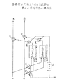
図3は、本発明のプリディストーション回路の第1の実施形態の構成図である。
【0039】
本実施形態は、可変減衰器の非線形性を考慮しない構成となっている。まず、同図(a)において、入力I信号が座標変換部1の端子Iに入力される。同じく、入力Q信号が座標変換部1の端子Qに入力される。この座標変換部1では、入力I信号と入力Q信号をI−Q平面上でのベクトルの座標値であると見なして、振幅r、位相θで表される局座標(r、θ)に変換する。I信号の信号値をI、Q信号の信号値をQで表すと、(I、Q)と(r、θ)とは、以下の式(3)、(4)で関係づけられる。
【0040】
【数2】
座標変換部1は、乗算器、加算器、除算器、及び平方根並びにtan関数の値を、それぞれ、保持するテーブルとからなっている。まず、座標変換部1では、I信号値とQ信号値の自乗を乗算器を使って算出する。次に、加算器を使って、それぞれの自乗値を加算し、各自乗値に対してその平方根の値が登録されているテーブルを参照して、式(3)で表されるr値を求める。次に、座標変換部1は、除算器を使って、Q信号値をI信号値で除算し、tan関数に関するテーブルを参照しθの値を求める。なお、これらの演算はソフトウェア処理により行っても良い。
【0042】
このようにして求められたr値とθ値は、座標変換部1の端子rと端子θからそれぞれ出力される。次に、r値は、加算器5に入力されると共に、前述のΔ関数値を出力するΔ関数加算部4に入力される。加算器5では、r値とΔ関数加算部4から入力される、このr値に対応するΔ関数値とが加算される。この操作は、上記式(1)の計算を行っていることに対応する。そして、加算器5によってプリディストーション処理が施された振幅値(r’値)は、座標変換部2の端子r’に入力される。また、本実施形態では、r値のみではなく、PAによって与えられる位相ずれに対するプリディストーションも行う構成となっている。
【0043】
位相θのプリディストーションとは、以下のようなものである。
【0044】
すなわち、PAの振幅及び位相に関する特性をプリディストーションによって補償する場合、PAの振幅に対する特性をf、位相に対する特性をφとし、PAに入力するI信号とQ信号のを複素数表示が、r・exp(jθ)で表されるものとする。ここで、jは虚数単位である。すると、PA通過後の信号は、f(r)・exp(j(θ+φ(r)))と表すことができる。次に、f(r)をべき級数展開したものの1次の項がc1 rとなったとすると(c1 は任意の定数)、プリディストーションとして次の関数を考える。
【0045】
【数3】
すると、PAに入力する信号は、r’・exp(jθ’)となるので、PAの出力信号は、f(r’)・exp(j(θ’+φ(r’)))となる。これを上記式(5)を使って変形すると、
【0047】
【数4】
となる。ここで、Vout は、PAの出力である。従って、プリディストーション関数を振幅r及び位相θに対して式(5)で定義すると、本来の入力r・exp(jθ)の定数倍(=c1 倍)の出力が得られることになる。すなわち、PAの特性を線形化することができる。上記式(5)から明らかなように、振幅rに対するプリディストーション関数Fpd(r)は、PAの特性の逆関数f-1(r’)の傾きをc1 だけ変更したものであるが、位相のプリディストーション関数θpd(r’)は、PAの位相特性φ(r’)を信号の位相θからそのまま引いたものでよいことが分かる。
【0049】
従って、位相プリディストーション部3では、座標変換部1から入力される位相値θから補償すべき回路の位相特性(PAのみとは限らない)φ(r’)を減算し、プリディストーション後の位相値として出力する。すなわち、θ−φ(r’)=θpd(r’)となる。このようにして得られたプリディストーション後の位相値θ’は、座標変換部2の端子θ’に入力される。ここで、位相のプリディストーション関数θpd(r’)は、それほど急峻な部分を持たないこと、及びPA等の位相特性が製品毎に異なるので、逐次実験などにより計測して定めるべきものである。そして、もし、位相のプリディストーション関数が急峻な傾きを持つものである場合には、振幅のプリディストーション関数に対して行った処理と同様な処理を適用するのが好ましい。座標変換部2では、r’、θ’に対して座標変換部1で行った処理と逆の処理を施してそれぞれ出力I’信号と出力Q’信号を出力する。座標変換部2の処理は、以下の式(7)で表される。
【0050】
【数5】
ここで、I’は、プリディストーション後のI信号値、Q’は、プリディストーション後のQ信号値である。ここでも、cos関数及びsin関数の各θ
’に対する値は、テーブル等に保持しておき、該テーブル等から読み出すことによって目的の信号値を得る。
【0052】
同図(b)は、Δ関数加算部4の内部構成を示す図である。式(2)に示したようにΔ関数は、最終的なプリディストーション関数であるδ関数にy=ax+bとの差分を加算したものである。従って、同図(b)では、入力振幅値に対し、δ関数加算部6によりδ関数値δpd(r)を出力すると共に、差分加算部7を設け、振幅値が所定値以上(式(2)では、xs 以上)の場合には、加算器8に差分加算部7から差分(=ax+b)を入力させて、該差分をδ関数値に加算して差分加算部7から出力する。ここで、y=ax+bの式において、xは入力振幅値rに等しく、また、a、bは、δ関数を作成する際に適切に選択された係数値であり、yが出力振幅値である。
【0053】
以上説明したように、図3の構成によって、入力I、Q信号に対して、プリディストーションをかけた出力I’、Q’信号が得られる。ここで、同図(b)のδ関数加算部6に記憶されているデジタル化されたδ関数の離散値は、δ関数の出力値の範囲が狭いのでデジタル化する際のビット数が少なくて済み、しかも量子化誤差を小さくすることができるので、メモリ容量を少なくして回路規模を小さくすると共に、精度の良いプリディストーションを行うことができる。
【0054】
図4は、本発明のプリディストーション回路の第2の実施形態を示す図である。
【0055】
図3の第1の実施形態では、座標変換部1によって、I信号とQ信号を振幅rと位相θに変換してプリディストーションを行ったが、第2の実施形態においては、I信号とQ信号とをr、θに変換しないでプリディストーションを行っている。
【0056】
ここで、I信号プリディストーション部10は、I信号に対するプリディストーションを行い、Q信号プリディストーション部11は、Q信号に対するプリディストーションを行う。同図では、それぞれの行うプリディストーション量は、ΔIpd(I、Q)、ΔQpd(I、Q)で表されている。ΔIpd(I、Q)、ΔQpd(I、Q)はFpd(x)と位相に関するプリディストーション関数θpd(x)により次のように定義された関数である。
【0057】
【数6】
ここで、I、Qは、それぞれI信号及びQ信号の信号値を表している。また、Fpd(x)については、式(1)、(2)で表されているように、δ関数のみをデジタル化(離散化)してテーブル形式に保持しておき、その他の演算は、演算器によって元のI信号及びQ信号を使って行い、最終的な関数値を得るようにする。これにより、前述したように、差分プリディストーション関数Δpd(x)の急峻な傾きを持つ部分については、補正関数δpd(x)により記憶し、該補正関数δpd(x)の出力値の範囲が狭いことを利用して、記憶容量を少なくすると共に、デジタル化の精度を高めるようにする。なお、cos関数やsin関数に関しては、やはりテーブルを用意しておき、テーブルから関数値を読みとるようにする。
【0059】
このようにして、I信号プリディストーション部10とQ信号プリディストーション部11で生成された信号値は、加算器12,13によって、それぞれI信号及びQ信号に加えられ、プリディストーション後の信号Ipd、Qpdとして出力される。なお、I信号プリディストーション部10及びQ信号プリディストーション部11は、ソフトウェアで実現することも可能である。
【0060】
図5は、本発明のプリディストーション回路の第3の実施形態を示す図である。
【0061】
なお、同図において、図3と同じ構成要素には同じ参照符号を付してある。
【0062】
座標変換部1に入力された入力I信号と入力Q信号は、振幅信号rと位相信号θに変換される。振幅信号rは、加算器5に入力されると共に、振幅プリディストーション部20に入力される。振幅プリディストーション部20は、振幅信号rを入力として、(Δpd(Gr))/Gを出力する。ここで、Gは、同図のプリディストーション回路の後段に設けられる可変減衰器(不図示)のゲインである。該ゲインGは、該可変減衰器の制御回路から振幅プリディストーション部20と乗算器21に入力される。振幅プリディストーション部20の出力は振幅信号rと加算器5で加算され、該加算結果が加算器5から座標変換部2の端子r’にプリディストーション後の振幅信号r’として入力される。また、振幅信号r’は、乗算器21にも入力され、乗算器21において可変減衰器のゲインGと乗算された後、位相プリディストーション部3に入力される。位相プリディストーション部3は、可変減衰器のゲインGが乗算されたプリディストーション後の振幅信号Gr’を基に、位相信号θ及び可変減衰器等のその他の構成要素の位相特性が校了された位相のプリディストーション量θpd(Gr’)を算出して、それをプリディストーション後の信号θ’として座標変換部2の端子θ’に入力する。
【0063】
座標変換部2は、入力された振幅信号r’と位相信号θ’とを基に、プリディストーション後のI信号I’及びQ信号Q’を生成し、出力する。
【0064】
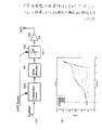
図6は、可変減衰器(VATT)のゲインGがプリディストーション関数に及ぼす影響について説明する図である。
【0065】
プリディストーション回路22への入力信号がr・exp(jθ)であるとすると、PA24の出力として欲しい信号はこの定数倍の信号であるGc1 r・exp(jθ)である。プリディストーション回路22の出力(▲3▼の信号)をr’・exp(jθ’)とすると、▲2▼の可変減衰器23の出力は、Gr’・exp(jθ’)となる。従って、PA24の出力▲1▼は、f(Gr’)・exp(j(θ’+φ(Gr’)))となる。これが、Gc1 r・exp(jθ)となるためには、次式(10)〜(12)を満たす必要がある。
【0066】
【数7】
ここで、Gは可変減衰器23のゲイン、r、θは、それぞれ、プリディストーション回路22の入力前の振幅信号及び位相信号、r’、θ’は、それぞれプリディストーション回路22によるプリディストーション後の振幅信号及び位相信号である。従って、行うべきプリディストーションは、式(11)と式(12)で与えられるので、これを実現するようにすればよい。
【0068】
図5によれば、振幅プリディストーション部20で(Δpd(Gr))/Gを求め、加算器5で振幅信号rと加算しているので、振幅プリディストーション部20と加算器5により式(12)のプリディストーションを行っていることになる。一方、乗算器21でGr’を求め、これを入力として、位相プリディストーション部3が位相のプリディストーションをおこなっているので、式(11)をこの位相プリディストーション部3の構成によって実現することができる。前述したように、この場合、位相プリディストーションは、元の位相信号θからPA24の位相特性値φ(Gr’)を減算するのみでよい。
【0069】
図7は、図5の振幅プリディストーション部20の内部構成を示した図である。
【0070】
なお、同図で図3(b)と同じ構成要素には同じ参照符号を付してある。
【0071】
Δ関数は、式(2)で与えられるので、図3(b)と同様に、δ関数加算部6と差分加算部7が設けられる。ただし、本実施形態の場合、δ関数の入力x及びy=ax+bの入力xは、可変減衰器のゲインGと振幅信号rとを乗算したものとなるので、可変減衰器のゲインを入力とし、乗算器25で振幅信号rと該ゲインGとを乗算して、その乗算結果をδ関数加算部6及び差分加算部7に入力させている。そして、図3(b)の場合と同様に、加算器8で、δ関数加算部6からの出力と差分加算部7の出力とを加算している。更に、式(12)で示されるように、Δ関数を1/G倍する必要があるので、入力された可変減衰器のゲインGをコンバータ27で1/Gに変換し、この変換結果を加算器8からの出力と乗算器26で乗算して、その乗算結果を出力する。
【0072】
図8は、本発明のプリディストーション回路の第4の実施形態を示す図である。
【0073】
同図において、図4と同じ構成要素には同じ参照符号を付してある。
【0074】
本実施形態の場合、入力したI信号とQ信号は、座標変換を施されずに、そのまま乗算器31,32にそれぞれ入力される。乗算器31,32には、可変減衰器のゲインGが入力され、乗算器31,32によりI信号及びQ信号がそれぞれG倍される。これらを入力として、I信号プリディストーション部10及びQ信号プリディストーション部11は、前述の式(8)及び式(9)で規定される演算を行い、ΔIpd値及びΔQpd値を出力する。これらの出力は、可変減衰器のゲインGが入力されるコンバータ30の出力1/Gと、乗算器33,34において乗算され、それぞれの乗算結果が加算器12,13でそれぞれ、I信号とQ信号に加算される。この加算処理の結果、プリディストーション後のI信号Ipd、及びプリディストーション後のQ信号Qpdがプリディストーション回路の出力として出力される。これらの一連の処理は、以下の式に示されるように表現され、式(13)及び式(14)が、それぞれ、前述の式(10)及び式(11)と同等であることが理解される。
【0075】
【数8】
なお、図4の説明で述べたとおり、I信号プリディストーション部10とQ信号プリディストーション部11は、sin関数及びcos関数の各テーブルを使い、それらに乗算器、減算器等を組み合わせてハードウェア的に構成しても良いし、CPUによるソフトウェア処理で実現するようにしても良い。
【0077】
図9は、本発明の実施形態において、A/D変換する際の方法について説明する図である。
【0078】
本発明の実施形態においては、入力信号と、入力信号に合成すべき差分プリディストーション信号(Δ関数など)を別々に扱うので、それぞれの量子化ビット数を独立に調整できる。そのため、差分プリディストーション信号のみ量子化ビット数を落として、関数テーブルに要する記憶素子の容量を削減する等の最適化が可能である。
【0079】
同図は、入力信号と差分プリディストーション信号の時間変化を模式的に図示したものであるが、前述の実施形態でも明らかなように、プリディストーション信号は、入力信号と差分プリディストーション信号を加算することによって得ている。従って、入力信号と差分プリディストーション信号を独立にA/D変換することが可能となる。例えば、入力信号に8ビット、差分プリディストーション信号に6ビットを割り振り、入力信号及び差分プリディストーション信号のアナログ信号をデジタル信号に変換すると、プリディストーション後の全体の信号は8ビット以上の精度でデジタル化されたことになり、より量子化誤差の少ないプリディストーション処理を行うことができる。しかも、関数テーブルを必要とする差分プリディストーション信号には6ビットのみが割り振られているので、関数テーブルの記憶容量を削減することができるという効果がある。
【0080】
図10は、本発明のプリディストーション回路の第5の実施形態を示す図である。
【0081】
本実施形態においては、プリディストーション回路41及び直交変調器42まで含めて全てCPU40によるデジタル信号処理で実装している。このような構成でもプリディストーション情報の圧縮は回路規模縮小のために有効である。CPU40は、入力されたベースバンドのI信号及びQ信号に対し、プリディストーション回路41が施すべき処理をソフトウェア処理によって実行する。更に、CPU40は、直交変調器(QPSKモジュレータ)42が行うQPSK変調処理もソフトウェア処理によって行う。このようにして得られた変調信号は、可変減衰器43に入力され、可変減衰器43により出力が調整された後、PA44によって増幅されて、アンテナ45から送信される。CPU40には、可変減衰器43のゲインを調整するゲイン情報(ゲインの値Gそのもの)等が入力され、前述したプリディストーション処理によりベースバンド信号のI、Q信号(ベースバンドI、Q信号)をプリディストーション処理する。そして、このプリディストーション処理されたI信号、Q信号にQPSK変調をかける。
【0082】
上述した記憶容量の圧縮法は、これまでアナログ回路で処理していた部分をデジタル信号処理に置き換える、いわゆるソフトウェア無線にも有効に使用できる。
【0083】
図11は、上記第5の実施形態においてCPU40が実行する処理の流れを示すフローチャートである。
【0084】
まず、ステップS1で、デジタル信号処理で、ベースバンド信号のI信号、Q信号及び可変減衰器のゲイン信号Gを取得する。次に、ステップS2において、I信号及びQ信号の信号値I、Qに前述の処理を施して、位相値θと振幅値rを求める。続いて、ステップS3で、上記位相θ、振幅rを基に、δpdに対応した関数テーブルを用いてプリディストーション後の振幅信号r’及び位相信号θ’を算出する。この算出のために使用される式は、以下のようになる。
【0085】
【数9】
なお、θpd(Gr)=θ−φ(Gr’)である。
ここで、定数a及びbは、δ関数の関数テーブルを作成する際に適切に設定される定数である。
【0087】
そして、ステップS4で、プリディストーション処理によって得られた振幅信号r’と位相信号θ’を使って、r’・cos(ωt+θ’)を算出して、これを図10には不図示のD/Aコンバータに出力する。ここで、ωは中間周波数または無線周波数に対応する角周波数であり、このcos(ωt+θ’)を算出することがQPSK変調に対応する。ステップS4で得られた変調信号は可変減衰器やPA等の後段のデバイスに送られて、アンテナから送信される。このとき、可変減衰器やPAの振幅特性や位相特性は、プリディストーションによって補償されているので、信号ひずみ及び隣接チャネル漏洩電力が抑制された信号がアンテナから送信される。
【0088】
図12は、本発明のプリディストーション回路の第6の実施形態を示す図である。
【0089】
前述の第1〜第5の実施形態では、入力信号をデジタル変換してから処理することを前提に説明してきたが、デジタル変換することによって量子化誤差が発生することを考慮すると、加算器に入力させる入力信号はデジタル化しない方が量子化誤差を発生しないので好ましい。
【0090】
従って、第6の本実施形態では、加算器に直接入力されるベースバンドI、Q信号はA/D変換せずに素通りさせ、これらのアナログ信号をD/A変換した差分プリディストーション信号(Δ関数値)とアナログ的に合成する。同図のプリディストーション関数はPAの前段にあるVATTやQPSKモジュレータの特性も補償する。
【0091】
すなわち、入力信号であるベースバンドI、Q信号はアナログ信号のままアナログ加算器53に入力される。一方、該アナログ入力I、Q信号は、A/D変換器50にも入力されて、A/D変換器50から入力されるデジタルのI、Q信号からデジタル信号に変換される。そして、差分プリディストーション部51において、デジタル的に記憶されているδ関数の関数テーブルを使って、差分プリディストーション信号Δpdをデジタル的に生成する。この差分プリディストーション信号Δpdは、D/A変換器52によってアナログ信号に変換され、入力ベースバンドI、Q信号とアナログ加算器53において加算される。
【0092】
このように、入力ベースバンド信号に関してはA/D変換せずにアナログ信号のまま直接アナログ加算器53に入力させ、このアナログの入力ベースバンドI、Q信号をアナログ信号に変換された差分プリディストーション信号Δpdとアナログ加算器53で合成するようにすれば、入力信号の量子化誤差をなくすことができ、特に、小信号時の特性を改善できる。
【0093】
図13は、本発明のプリディストーション回路の第7の実施形態を説明する図である。
【0094】
前述までのプリディストーション回路の実施形態では、プリディストーション処理を、PAの振幅、位相特性、及び可変減衰器のゲインを考慮して行えば、より効果的にプリディストーションが行われることを述べた。第7の実施形態では、更に、直交変調器56がプリディストーション回路55と別装置として設けられる場合、この直交変調器56の振幅、位相特性も考慮してプリディストーションを行うようにする。この場合には、直交変調器56の振幅、位相特性を実験的に求めておき、プリディストーション回路55の差分プリディストーション関数の関数テーブルの格納データを、実験的に求められた直交変調器56の振幅、位相特性も含めてプリディストーションされるように変更しておく。このようにすることによって、プリディストーション回路55の後段の全ての装置(直交変調器56,可変減衰器57、PA58)の特性を全て補償した信号をアンテナ59から送信することができる。すなわち、信号ひずみや隣接チャネル漏洩電力の抑制された信号を送出することができるので、より品質の高い通信を行うことができる。
【0095】
また、同図には示されていないが、上記各装置に加え、実際の回路には含まれるであろう、A/D変換器等も含めて、振幅、位相特性を測定しておき、それらの測定結果を差分プリディストーション関数に反映させることにより、更に、より品質の良い信号を送受信することが可能となる。
【0096】
図14は、本発明のプリディストーション回路の第8の実施形態を示す図である。
【0097】
本実施形態では、差分プリディストーション回路60により振幅の補償(プリディストーション)をした後、RF移相器62により位相の補償(プリディストーション)をしている。
【0098】
すなわち、振幅の補償のみベースバンドで行い、位相の補償はRFのアナログ移相器により補償する。これにより、やや回路規模の大きいデジタル乗算器が複数必要となるベースバンド移相器を使わずに済むので、全体の回路規模を縮小できる。
【0099】
本実施形態の構成は同図(a)に示されている。
【0100】
入力されたベースバンドのI、Q信号は、直接アナログ加算器67に入力されると共に、差分プリディストーション回路60にも入力される。差分プリディストーション回路60は、振幅のプリディストーション信号を出力し、出力されたプリディストーション信号は加算器67において、入力ベースバンドI、Q信号と加算される。なお、同図では、A/D変換器、D/A変換器は省略されている。A/D変換器やD/A変換器は、差分プリディストーション回路60の前後に設けられる。あるいは、ベースバンドの入力I、Q信号を一旦デジタル信号に変換してから、差分プリディストーション回路60により振幅値のプリディストーションを行い、デジタル方式に置き換えた加算器67の加算結果をD/A変換してアナログ信号に変換するようにしても良い。
【0101】
加算器67の出力は、直交変調器61でRF信号に変調されて、RF移相器62に入力される。また、加算器67の出力は、位相プリディストーション回路63にも入力され、位相プリディストーション回路63により生成された位相に対するプリディストーション信号がRF移相器62に入力される。RF移相器62は、変調されたRF信号の位相をシフトして出力する。これにより、位相のプリディストーションが行われる。このようにして、振幅及び位相にプリディストーションが施された信号は、可変減衰器64で電力が調整され、PA65で増幅されて、アンテナ66から送信されていく。
【0102】
同図(b)は、上記RF移相器62の構成例を示す図である。
【0103】
直交変調器61から出力されたRF信号は、RF移相器62のハイブリッド70の端子aに入力される。ハイブリッド70に入力されたRF信号は、分岐されて端子c、dから出力される。端子c、dには、それぞれコンデンサ72−1、72−2の一端が接続されている。該コンデンサ72−1、72−2の他端には、それぞれ、アノードが接地された可変容量ダイオードであるダイオード73−1、73−2のカソードが接続されている。位相のプリディストーション信号θpdは、同図(b)に示すように、コンデンサ72−1とダイオード73−1の間、及びコンデンサ72−2と、ダイオード73−2の間に印可される。これにより、コンデンサ72−1、72−2の接地側の電圧が双方で異なることになる。
端子c、dから出力されたRF信号は、それぞれのコンデンサ72−1、72−2で反射されるが、コンデンサ72−1の接地側の電圧とコンデンサ72−2の接地側の電圧との差によって反射される際に、位相差を生じる。このようにして、反射されたRF信号はそれぞれ、端子c、dに入力される。そして、上記のように生成された位相差によって、入力RF信号に対して位相がシフトしたRF信号がハイブリッド70の端子bから出力される。以上のようにして、RF移相器62では、RF信号の位相を変化させて出力することができる。
【0104】
なお、ハイブリッド70及びバリキャップ71の動作の詳細については、当業者によれば容易に理解されるであろう。
【0105】
図15は、本発明のプリディストーション回路の第9の実施形態を示す図である。
【0106】
なお、同図において、図14(a)と同じ構成要素には同じ参照符号を付してある。
【0107】
本実施形態においては、差分プリディストーション回路60により振幅の補償をした後、直交変調器61における局部発振器75(前述の実施形態の図面では図示を省略していたが、実際には、ベースバンド信号をIF信号に変換する場合や、RF信号に変換する場合に通常設けられる)の発信信号の位相を変化させることによりIF信号の位相にプリディストーションをかけている。
【0108】
入力されたベースバンドI、Q信号は加算器67に入力されると共に、差分プリディストーション回路60にも入力される。差分プリディストーション回路60の出力は加算器67に入力され、加算器67において、入力I、Q信号に加算される。なお、図14(a)の場合と同様に、図15においても、A/D変換器、D/A変換器の図示が省略されている。
【0109】
加算器67の出力は、直交変調器61に入力され、直交変調される。また、加算器67の出力は、分岐されて、位相プリディストーション回路63にも入力される。位相プリディストーション回路63は、ベースバンドI、Q信号に与えるべき位相プリディストーション量を示す信号を直交変調器61の局部発振器75に与え、局部発振器75の出力する信号の位相を変化させる。局部発振器75の出力の位相を変化させることによって、直交変調器61で変調されるベースバンドI、Q信号の位相が調整され、ちょうど位相プリディストーションをかけた場合と同じ効果を得ることができる。このようにして生成されたIF変調信号は、不図示のIF/RF変換器を介して可変減衰器64に入力され、可変減衰器64において出力が調整された後、PA65で増幅され、アンテナ66から送信される。
【0110】
なお、本実施形態では、局部発振器75は、IF周波数の信号を出力するものとしている。
【0111】
図16は、本発明のプリディストーション回路の第10の実施形態を示す図である。
【0112】
なお、同図において、図14(a)と同じ構成要素には同じ参照符号を付している。
【0113】
本実施形態においては、差分プリディストーション回路60により振幅の補償をした後、周波数混合器77における局部発振器76の位相を変化させることによりRF信号の位相のプリディストーションを行っている。
【0114】
入力したベースバンドI、Q信号は、差分プリディストーション回路60と加算器67によって、振幅のプリディストーションがかけられる。なお、前述した第8及び第9の実施形態の場合と同じように、この構成においてもA/D変換器、及びD/A変換器の図示が省略されている。
【0115】
加算器67の出力は、直交変調器61によって変調され、IF信号に変換される。なお、図16の構成では、図15に示した直交変調器61の局部発振器を位相シフトに使用しないので、該局部発振器については図示を省略している。直交変調器61から出力されたIF信号は、周波数混合器77に入力される。一方、分岐された加算器67の出力は、位相プリディストーション回路63に入力され、位相プリディストーション回路63により生成された位相プリディストーション信号が局部発振器76に入力される。局部発振器76は、IF信号をRF信号に変換するためのもので、RF周波数帯の信号を出力する。局部発振器76は、位相プリディストーション回路63からの位相プリディストーション信号に基づいて、出力するRF周波数帯の信号の位相をシフトして、周波数混合器77に供給する。これにより、直交変調器61から出力されたIF信号は、周波数混合器77においてRF信号に変換されるとともに、位相プリディストーションを受け、可変減衰器64に入力される。そして、可変減衰器64で出力が調整されたRF信号は、PA65で増幅されて、アンテナ66から送信される。
【0116】
図17は、第9及び第10の実施形態における各局部発振器75,76の構成を示す図である。
【0117】
振幅プリディストーション処理を施されたベースバンド信号のI信号とQ信号が振幅値算出部80の端子I’と端子Q’にそれぞれ入力されると、振幅値算出部80において該入力されたI信号とQ信号から振幅値r’が算出される。上述した第9及び第10の実施形態の構成図15,16では、この振幅値算出部80が示されていないが、図示が省略されているのみであって、実際には、同図の構成に従って設けられるべきものである。
【0118】
振幅値算出部80で算出された振幅値r’は、位相プリディストーション回路81に入力され、位相プリディストーション回路81において位相プリディストーション信号θpdが生成される。該位相プリディストーション信号θpdは、位相値変換部82において、cosθpd、sinθpdに変換され、該cosθpd、sinθpdが乗算器83,84にそれぞれ入力される。発振器86からは、所定の周波数ωの正弦波cos(ωt)が出力される。同図の局部発振器86がベースバンド信号をIF帯域の信号に変換するために用いられるか(局部発振器75の場合)、あるいは、IF帯域からRF帯域に信号を変換するために用いられるか(局部発振器76)によって、正弦波cos(ωt)の角周波数ωの値は適宜設定されるべきものである。局部発振器86から出力された正弦波cos(ωt)は、乗算器84に直接入力されると共に、90°移相器85によって位相が90°シフトされてsin(ωt)に変換され、乗算器83に入力される。それぞれ、乗算器83、84に入力されたsin(ωt)、cos(ωt)は、乗算器83,84において位相値変換部82からの出力とそれぞれ乗算され、各乗算結果が、加算器87で加算される。これにより、加算器87において以下の式の左辺に示す演算が行われ、位相プリディストーション値θpdだけ移相された周期波sin(ωt+θpd)が生成される。
【0119】
cosθpd・sin(ωt)+sinθpd・cos(ωt)=sin(ωt+θpd)
以上のようにして、位相がシフトされた周期波sin(ωt+θpd)を使用して、直交変調あるいは、周波数混合を行うことによって、生成される信号は、位相プリディストーション値θpdの分だけ位相シフトされているので、第9及び第10の実施形態において位相プリディストーションを効率よくかけることができる。
【0120】
なお、上述した本発明の各実施形態は、通信システムにおける送信機に設けられる電力増幅器を前提とするものであるが、本発明のプリディストーション装置あるいはプリディストーション方法は、通信システムでない他のシステムの一部に設けられる増幅器にも適用可能である。
【0121】
【発明の効果】
本発明によれば、プリディストーション信号の入力信号に対する差分に関する情報のみを記録する、あるいは、その差分関数を近似関数(y=ax+b)と補正関数に分離し、該補正関数に関する情報のみを記録することにより、プリディストーション処理のために必要となる情報の記憶容量を減らすことができ、プリディストーションを実装する装置の回路規模を縮小できる。
【図面の簡単な説明】
【図1】本発明の実施形態の基本的原理を説明する図(その1)である。
【図2】本発明の実施形態の基本的原理を説明する図(その2)である。
【図3】本発明のプリディストーション回路の第1の実施形態の構成図である。
【図4】本発明のプリディストーション回路の第2の実施形態の構成図である。
【図5】本発明のプリディストーション回路の第3の実施形態の構成図である。
【図6】可変減衰器のゲインがプリディストーション関数に及ぼす影響について説明する図である。
【図7】図5の振幅プリディストーション部20の構成を示した図である。
【図8】本発明のプリディストーション回路の第4の実施形態の構成図である。
【図9】本発明の実施形態において、A/D変換する際の方法について説明する図である。
【図10】本発明のプリディストーション回路の第5の実施形態の構成図である。
【図11】第5の実施形態におけるCPUの実行処理の流れを示すフローチャートである。
【図12】本発明のプリディストーション回路の第6の実施形態の構成図である。
【図13】本発明のプリディストーション回路の第7の実施形態の構成図である。
【図14】本発明のプリディストーション回路の第8の実施形態の構成図である。
【図15】本発明のプリディストーション回路の第9の実施形態の構成図である。
【図16】本発明のプリディストーション回路の第10の実施形態の構成図である。
【図17】第9及び第10の実施形態における局部発振器の構成を示す図である。
【図18】電力増幅器の入出力特性を示す図である。
【図19】プリディストーション方式を説明する図である。
【図20】可変減衰器の減衰特性も含めてプリディストーションで補償しようとする場合の構成及び特性を示した図である。
【符号の説明】
1、2 座標変換部
3、63、81 位相プリディストーション部(回路)
4 Δ関数加算部
5、8、12、13、53、87 加算器
6 δ関数加算部
7 差分加算部
10 I信号プリディストーション部
11 Q信号プリディストーション部
20 振幅プリディストーション部
21、25、26、31、32、33、34、77、83、84 乗算器
27、30 コンバータ
41、55 プリディストーション回路
42、56、61 QPSKモジュレータ(直交変調器)
43、57、64 可変減衰器
44、58、65 電力増幅器(PA)
45、59、66 アンテナ
50 A/D変換器
51、60 差分プリディストーション部
52 D/A変換器
62 RF移相器
70 ハイブリッド
71 バリキャップ
72−1、72−2 コンデンサ
73−1、73−2 ダイオード
75、76 局部発振器
80 振幅値算出部
82 位相値変換部
85 90°移相器
86 発振器[0001]
BACKGROUND OF THE INVENTION
The present invention relates to a technique for linearizing input / output characteristics of a power amplifier.
[0002]
[Prior art]
In mobile communication, a signal outside the use band becomes an interference wave to the adjacent channel, and therefore it is necessary to ensure sufficient linearity in the power amplifier in order to keep the signal power outside the use band low. For this reason, the output back-off method that suppresses the output power until the out-of-band power becomes sufficiently small has been used in the past, but this method is a trade-off between efficiency and linearity, so that efficiency is ensured. However, it is difficult to improve linearity.
[0003]
FIG. 18 is a diagram illustrating input / output characteristics of a typical power amplifier.
[0004]
The output back-off method will be described with reference to FIG.
[0005]
When the output of the power amplifier increases, the relationship between the input and output of the power amplifier deviates from the linear relationship as shown in (2) of FIG. 18, as shown by the curve of (1) of FIG. Therefore, in the output back-off method, only a portion with a small input power that maintains linearity is used in the curve (1) that is a characteristic curve of an actual power amplifier. Of the characteristic curve of the power amplifier, the portion where the input power is small behaves close to the ideal characteristic curve (2) as shown in the figure, so that sufficient linearity is obtained from the operation of the power amplifier. The generation of high frequency components due to the deterioration of the waveform of the obtained signal to be amplified, that is, the generation of noise in the adjacent channel can be suppressed.
[0006]
However, since the amplification efficiency of the power amplifier becomes small when the input power is small, there is a problem that the power amplifier cannot be used with sufficient efficiency. In order to improve the amplification efficiency, the input power must be increased. However, the nonlinearity of the power amplifier becomes a problem. Therefore, in the output back-off method, efficiency and linearity are traded off, and it is difficult to achieve both high efficiency and linearity.
[0007]
[Problems to be solved by the invention]
As a method for improving linearity while ensuring amplification efficiency, linearization by a predistortion method has been attempted. For details of this method, see, for example, the specification of Japanese Patent Application No. 9-297297 filed earlier by the present applicant.
[0008]
FIG. 19 is a diagram for explaining the predistortion method.
[0009]
As shown in FIG. 5A, when predistorting the input / output characteristics of the power amplifier (PA), baseband I and Q signals are input to the
[0010]
When the predistortion method is implemented by a digital circuit, if an attempt is made to deal with a wide power range only by digital signal processing with the configuration as shown in FIG. 19A, the quantization error increases at the time of low power, and the adjacent channel leakage power. (ACP) characteristics are significantly deteriorated. That is, F in FIG. pd When the values of the function for applying predistortion such as (x) are discretized, the values are held in a table, and the values corresponding to the input signal values are read from the table, the input signal having a small slope in the function The signal corresponding to the portion where the power is small is too discretized with respect to the slope of the function, and predistortion with a large error is applied to the value of the input signal that changes in an analog manner. End up.
[0011]
FIG. 5B is a diagram showing the state of adjacent channel leakage power (ACP) with respect to the output of the
[0012]
As indicated by ○ and + in FIG. 5B, when predistortion is not performed, the adjacent channel leakage power (ACP) increases as the output power Pout of the
[0013]
Thus, in order to improve the ACP, it is conceivable to increase the number of input / output bits for discretizing the predistortion function, but in that case, the circuit scale becomes large.
[0014]
In the configuration shown in FIG. 9A, the attenuation characteristic of the variable attenuator (VATT) 180 is not taken into consideration, and thus there is a problem that the ACP is further deteriorated.
[0015]
FIG. 20 is a diagram showing a configuration and characteristics when compensation is made by predistortion in consideration of attenuation characteristics of the variable attenuator.
[0016]
In the configuration of FIG. 5A, predistortion is performed on the baseband I signal and Q signal by the
[0017]
FIG. 5B is a diagram showing the relationship between the output power value to
[0018]
The meaning of each curve in FIG. 19B is the same as that in FIG. As is apparent from FIG. 5B, the ACP characteristic is improved by applying predistortion compared to the case where predistortion is not applied. In addition, the larger the number of bits when digitizing the predistortion function, the better the ACP characteristic. Further, when comparing the ACP characteristic when the predistortion shown in FIG. 19B is applied with the ACP characteristic when the predistortion shown in FIG. 20B is applied, FIG. As in a), it is understood that the ACP characteristic is improved in the configuration in which the attenuation characteristic of the
[0019]
Therefore, if the output power is adjusted by the
[0020]
In particular, when considering application to mobile communication terminals, miniaturization and weight reduction and low power consumption are major targets. Therefore, the circuit scale can be reduced by compressing predistortion information using a simple method that does not increase the circuit scale. It needs to be small.
[0021]
An object of the present invention is to provide an apparatus and a method capable of performing accurate predistortion without increasing the circuit scale.
[0022]
[Means for Solving the Problems]
A predistortion device according to the present invention is a predistortion device for linearizing input / output characteristics of a power amplifier. A predistortion function for linearizing input / output characteristics of a power amplifier and a function represented by a predetermined expression Difference predistortion means for generating a differential predistortion signal using the differential predistortion function for the input signal, the differential predistortion signal, and the input signal And synthesizing means for outputting a signal obtained by the synthesis as a signal after predistortion.
[0023]
The predistortion method of the present invention is a predistortion method for linearizing input / output characteristics of a power amplifier, and is represented by (a) a predistortion function for linearizing input / output characteristics of a power amplifier and a predetermined expression. A difference pre-distortion function is used as a difference pre-distortion function, and a difference pre-distortion signal is generated using the difference pre-distortion function for the input signal; and (b) the difference pre-distortion signal; Synthesizing with the input signal, and outputting the signal obtained by the synthesis as a predistorted signal.
[0024]
According to the present invention, a predistortion function having a steep slope is converted into a differential predistortion function obtained by a difference between the function and another appropriate function, and the differential predistortion function is digitized and held. Therefore, when the function table of the differential predistortion function is created, the information of the differential predistortion function can be digitized more accurately with a small number of bits.
[0025]
Therefore, when performing predistortion using this function table, the quantization error can be reduced, and the number of bits required to hold the information can be reduced, so the storage capacity of the storage element that stores the function table Therefore, the circuit scale of the predistortion circuit can be reduced. Therefore, an accurate predistortion device can be realized with a small configuration.
[0026]
DETAILED DESCRIPTION OF THE INVENTION
In the present invention, in order to reduce the scale of the digital signal processing circuit used in the predistortion method, only the difference between the predistortion signal and the input signal is recorded in the storage element, thereby compressing the storage capacity of the function table. Furthermore, this difference function is separated into an approximate function and its correction function, and only the information of the correction function is held in the storage element, thereby further reducing the storage capacity of the function table.
[0027]
In this case, a method of processing the complex baseband I signal and Q signal after converting them into amplitude and phase, and a method of processing the complex baseband I signal and Q signal without converting them into amplitude and phase However, if conversion into amplitude and phase is performed, the storage capacity of the function table can be further reduced.
[0028]
1 and 2 are diagrams for explaining the basic principle of the embodiment of the present invention.
[0029]
The predistortion function necessary for linearizing the power amplifier (PA) having the characteristics shown in FIG. 18 (1) as shown in FIG. 18 (2) is F in FIG. pd (X) and this function F pd (X) is obtained by multiplying the inverse function of the function indicating the input / output characteristics of (1) in FIG. 18 by a constant. This function F pd (X) is a function that has a relatively gentle slope when the input is small and increases with a steep slope when the input becomes larger than a certain level. In practice, an upper limit is set for the maximum value of the output of the PA. However, in order to improve the efficiency of the PA, it is necessary to increase the upper limit to some extent.
[0030]
This function F pd When (x) is discretized and used, the problem is that most of the discretized output information is assigned to the steep portion (1), so that the substantial quantization bit in the portion (2) having a small amplitude. The number cannot be secured. In FIG. 1, since the portion (2) is almost ¼ of the entire portion, this portion loses the number of quantization bits of about 2 bits, which causes deterioration of characteristics at the time of a small signal.
[0031]
That is, as shown by the four dotted lines in FIG. 1, when the output value Pout of the PA is discretized at four intervals, three discrete values are given to the part (1). One of three discrete values can be output in response to the change of the value Pin. However, in the part (2), since the inclination of the graph is small, only one discrete value is assigned. Therefore, even if the input value Pin of PA changes, the digitized function value F output for the portion (2). pd (X) outputs only one specific value. Thus, the predistortion function F pd (X) cannot output a correct value by digitization, and this phenomenon causes a quantization error and deteriorates adjacent channel leakage power (ACP) characteristics.
[0032]
Therefore, instead of recording the entire predistortion function, the difference between the predistortion function and the input signal is recorded. That is, F pd A function Δ of only the difference obtained by subtracting y = x from (x) pd (X) = F pd (X) -x is discretized and used. Here, since the function y = x outputs the input x as it is as the output y, it actually represents the input signal itself. As shown in FIG. 1, the function y = x is changed to a predistortion function F. pd By subtracting from (x), the input signal can be handled separately, so that the characteristics can be improved particularly when the amplitude is small (part (2) in FIG. 1). In the following, Δ pd For convenience, (x) is often expressed as a Δ function.
[0033]
FIG. 2 shows the predistortion function F obtained as described above. pd Difference function Δ between (x) and input signal pd It is a figure explaining the method of further separating and expressing (x).
[0034]
As shown in the figure, Δ pd Since a portion with a steep slope remains in (x), the number of output bits is still used to express the steep portion, and the digitization accuracy of the portion with the gentle slope is not good. Therefore, paying attention to the fact that the change in the slope of this steep portion is relatively small, only this portion takes a difference from the straight line y = ax + b.
Δ which is a correction function obtained as a result of such processing pd (X) (hereinafter referred to as δ function for convenience) is the original Δ pd Since the amplitude (range of the output value Pout) is compressed compared to (x), a large number of bits can be assigned to a narrow output range, and the original predistortion function F pd Compared with the case where the entire output range of (x) is digitized, it can be digitized with a smaller number of bits. As a result, the necessary storage capacity can be compressed. Original predistortion function F pd (X) is Δ pd It can be expressed by the following formulas (1) and (2) using (x).
[0035]
[Expression 1]
The operations appearing in these equations are only sums and products, and their operation circuits can be realized with a relatively small circuit. Moreover, you may perform those calculations with software. Here, a, b, and xs are constants that are appropriately determined when the δ function is created.
[0037]
Further, as in the case of FIG. 19, not only the power amplifier but also a circuit including a non-linear characteristic of a quadrature modulator, a gain control amplifier (AGC: or power amplifier PA), a frequency mixer, and a variable attenuator can be compensated. The overall linearity can be improved without increasing the scale.
[0038]
FIG. 3 is a block diagram of the first embodiment of the predistortion circuit of the present invention.
[0039]
This embodiment has a configuration that does not consider the nonlinearity of the variable attenuator. First, in FIG. 2A, an input I signal is input to the terminal I of the coordinate
[0040]
[Expression 2]
The coordinate
[0042]
The r value and the θ value obtained in this way are output from the terminal r and the terminal θ of the coordinate
[0043]
The pre-distortion of the phase θ is as follows.
[0044]
That is, when the characteristics related to the amplitude and phase of the PA are compensated by predistortion, the characteristic with respect to the amplitude of the PA is f, the characteristic with respect to the phase is φ, and the complex number display of the I signal and the Q signal input to the PA is given by r · exp It is represented by (jθ). Here, j is an imaginary unit. Then, the signal after passing through PA can be expressed as f (r) · exp (j (θ + φ (r))). Next, the first order term of the power series expansion of f (r) is c 1 If r becomes (c 1 Is an arbitrary constant), and consider the following function as predistortion:
[0045]
[Equation 3]
Then, since the signal input to the PA is r ′ · exp (jθ ′), the output signal of the PA is f (r ′) · exp (j (θ ′ + φ (r ′))). If this is transformed using the above equation (5),
[0047]
[Expression 4]
It becomes. Here, Vout is the output of PA. Therefore, when the predistortion function is defined by the equation (5) with respect to the amplitude r and the phase θ, a constant multiple of the original input r · exp (jθ) (= c 1 Output). That is, PA characteristics can be linearized. As is clear from the above equation (5), the predistortion function F with respect to the amplitude r. pd (R) is an inverse function f of the characteristic of PA. -1 The slope of (r ′) is c 1 The phase predistortion function θ pd It can be seen that (r ′) may be obtained by subtracting the phase characteristic φ (r ′) of PA from the phase θ of the signal as it is.
[0049]
Accordingly, the
[0050]
[Equation 5]
Here, I ′ is the I signal value after predistortion, and Q ′ is the Q signal value after predistortion. Again, each cos function and sin function θ
The value for 'is held in a table or the like, and the target signal value is obtained by reading from the table or the like.
[0052]
FIG. 2B is a diagram showing the internal configuration of the Δ
[0053]
As described above, with the configuration of FIG. 3, the output I ′ and Q ′ signals obtained by predistorting the input I and Q signals are obtained. Here, the discrete value of the digitized δ function stored in the δ function adding unit 6 in FIG. 5B has a small range of output values of the δ function, so that the number of bits when digitizing is small. In addition, since the quantization error can be reduced, the memory capacity can be reduced, the circuit scale can be reduced, and predistortion with high accuracy can be performed.
[0054]
FIG. 4 is a diagram showing a second embodiment of the predistortion circuit of the present invention.
[0055]
In the first embodiment of FIG. 3, the I and Q signals are converted into the amplitude r and the phase θ by the coordinate
[0056]
Here, the I
[0057]
[Formula 6]
Here, I and Q represent signal values of the I signal and the Q signal, respectively. F pd As for (x), as expressed by equations (1) and (2), only the δ function is digitized (discretized) and held in a table format, and other operations are performed by an arithmetic unit. This is done using the original I and Q signals to obtain the final function value. Thus, as described above, the differential predistortion function Δ pd For a portion with a steep slope of (x), the correction function δ pd (X) to store the correction function δ pd By utilizing the fact that the range of the output value of (x) is narrow, the storage capacity is reduced and the digitization accuracy is increased. As for the cos function and sin function, a table is prepared, and the function value is read from the table.
[0059]
In this way, the signal values generated by the I
[0060]
FIG. 5 is a diagram showing a third embodiment of the predistortion circuit of the present invention.
[0061]
In the figure, the same components as those in FIG. 3 are denoted by the same reference numerals.
[0062]
The input I signal and the input Q signal input to the coordinate
[0063]
The coordinate
[0064]
FIG. 6 is a diagram for explaining the influence of the gain G of the variable attenuator (VATT) on the predistortion function.
[0065]
Assuming that the input signal to the
[0066]
[Expression 7]
Here, G is the gain of the
[0068]
According to FIG. 5, the amplitude predistortion unit 20 (Δ pd Since (Gr)) / G is obtained and added to the amplitude signal r by the adder 5, the predistortion of Expression (12) is performed by the
[0069]
FIG. 7 is a diagram illustrating an internal configuration of the
[0070]
In the figure, the same components as those in FIG. 3B are denoted by the same reference numerals.
[0071]
Since the Δ function is given by equation (2), a δ function addition unit 6 and a
[0072]
FIG. 8 is a diagram showing a fourth embodiment of the predistortion circuit of the present invention.
[0073]
In the figure, the same components as those in FIG. 4 are denoted by the same reference numerals.
[0074]
In this embodiment, the input I signal and Q signal are input to the
[0075]
[Equation 8]
As described in the description of FIG. 4, the I
[0077]
FIG. 9 is a diagram illustrating a method for A / D conversion in the embodiment of the present invention.
[0078]
In the embodiment of the present invention, since the input signal and the differential predistortion signal (Δ function or the like) to be combined with the input signal are handled separately, the number of quantization bits can be adjusted independently. Therefore, optimization such as reducing the number of quantization bits of only the differential predistortion signal and reducing the storage element capacity required for the function table is possible.
[0079]
The figure schematically shows the temporal change of the input signal and the differential predistortion signal. As is clear from the previous embodiment, the predistortion signal adds the input signal and the differential predistortion signal. By gaining. Therefore, it becomes possible to A / D-convert the input signal and the differential predistortion signal independently. For example, if 8 bits are assigned to the input signal and 6 bits are assigned to the differential predistortion signal, and the analog signal of the input signal and differential predistortion signal is converted to a digital signal, the entire signal after predistortion is digital with an accuracy of 8 bits or more. Thus, predistortion processing with less quantization error can be performed. In addition, since only 6 bits are allocated to the differential predistortion signal that requires the function table, the storage capacity of the function table can be reduced.
[0080]
FIG. 10 is a diagram showing a fifth embodiment of the predistortion circuit of the present invention.
[0081]
In this embodiment, the
[0082]
The storage capacity compression method described above can also be used effectively for so-called software defined radio, which replaces a portion processed by an analog circuit so far with digital signal processing.
[0083]
FIG. 11 is a flowchart showing a flow of processing executed by the
[0084]
First, in step S1, the baseband signal I signal and Q signal and the variable attenuator gain signal G are acquired by digital signal processing. Next, in step S2, the signal values I and Q of the I signal and Q signal are subjected to the above-described processing to obtain the phase value θ and the amplitude value r. Subsequently, in step S3, based on the phase θ and the amplitude r, δ pd A predistorted amplitude signal r ′ and phase signal θ ′ are calculated using a function table corresponding to. The formula used for this calculation is as follows:
[0085]
[Equation 9]
Θ pd (Gr) = θ−φ (Gr ′).
Here, the constants a and b are constants that are appropriately set when the function table of the δ function is created.
[0087]
In step S4, r ′ · cos (ωt + θ ′) is calculated using the amplitude signal r ′ and the phase signal θ ′ obtained by the predistortion process, and this is calculated as D / D not shown in FIG. Output to A converter. Here, ω is an angular frequency corresponding to the intermediate frequency or the radio frequency, and calculating this cos (ωt + θ ′) corresponds to QPSK modulation. The modulated signal obtained in step S4 is sent to a subsequent device such as a variable attenuator or PA and transmitted from the antenna. At this time, since the amplitude characteristic and phase characteristic of the variable attenuator and PA are compensated by predistortion, a signal in which signal distortion and adjacent channel leakage power are suppressed is transmitted from the antenna.
[0088]
FIG. 12 is a diagram showing a sixth embodiment of the predistortion circuit of the present invention.
[0089]
In the first to fifth embodiments described above, the description has been made on the assumption that the input signal is processed after being digitally converted. However, in consideration of the occurrence of a quantization error due to the digital conversion, the adder includes It is preferable not to digitize the input signal to be input because a quantization error does not occur.
[0090]
Therefore, in the sixth embodiment, the baseband I and Q signals input directly to the adder are passed without being A / D converted, and these analog signals are D / A converted differential predistortion signal (Δ Function value) and analog. The predistortion function shown in the figure also compensates for the characteristics of the VATT or QPSK modulator in the preceding stage of the PA.
[0091]
That is, the baseband I and Q signals that are input signals are input to the
[0092]
As described above, the input baseband signal is directly input to the
[0093]
FIG. 13 is a diagram for explaining a seventh embodiment of the predistortion circuit of the present invention.
[0094]
In the embodiments of the predistortion circuit described above, it has been described that predistortion is performed more effectively if the predistortion processing is performed in consideration of the amplitude of the PA, the phase characteristic, and the gain of the variable attenuator. In the seventh embodiment, when the
[0095]
Although not shown in the figure, amplitude and phase characteristics including A / D converters and the like that will be included in the actual circuit in addition to the above-described devices are measured, and these are measured. By reflecting this measurement result in the differential predistortion function, it becomes possible to transmit / receive a signal of higher quality.
[0096]
FIG. 14 is a diagram showing an eighth embodiment of the predistortion circuit of the present invention.
[0097]
In the present embodiment, amplitude compensation (predistortion) is performed by the
[0098]
That is, only amplitude compensation is performed in the baseband, and phase compensation is performed by an RF analog phase shifter. As a result, it is not necessary to use a baseband phase shifter that requires a plurality of digital multipliers having a slightly larger circuit scale, so that the entire circuit scale can be reduced.
[0099]
The configuration of this embodiment is shown in FIG.
[0100]
The input baseband I and Q signals are directly input to the
[0101]
The output of the
[0102]
FIG. 5B is a diagram showing a configuration example of the
[0103]
The RF signal output from the
The RF signals output from the terminals c and d are reflected by the capacitors 72-1 and 72-2, respectively, but the difference between the voltage on the ground side of the capacitor 72-1 and the voltage on the ground side of the capacitor 72-2. Produces a phase difference when reflected by. In this way, the reflected RF signals are input to the terminals c and d, respectively. Then, an RF signal whose phase is shifted with respect to the input RF signal due to the phase difference generated as described above is output from the terminal b of the hybrid 70. As described above, the
[0104]
Details of the operation of the hybrid 70 and the
[0105]
FIG. 15 is a diagram showing a ninth embodiment of the predistortion circuit of the present invention.
[0106]
In the figure, the same components as those in FIG. 14A are denoted by the same reference numerals.
[0107]
In this embodiment, after the amplitude is compensated by the
[0108]
The input baseband I and Q signals are input to the
[0109]
The output of the
[0110]
In the present embodiment, the
[0111]
FIG. 16 is a diagram showing a tenth embodiment of the predistortion circuit of the present invention.
[0112]
In the figure, the same components as those in FIG. 14A are denoted by the same reference numerals.
[0113]
In the present embodiment, after the amplitude is compensated by the
[0114]
The input baseband I and Q signals are subjected to amplitude predistortion by a
[0115]
The output of the
[0116]
FIG. 17 is a diagram showing the configuration of the
[0117]
When the I signal and the Q signal of the baseband signal subjected to the amplitude predistortion process are respectively input to the terminal I ′ and the terminal Q ′ of the amplitude value calculation unit 80, the input I signal is input to the amplitude value calculation unit 80. And the amplitude value r ′ is calculated from the Q signal. In the configuration diagrams 15 and 16 of the ninth and tenth embodiments described above, the amplitude value calculation unit 80 is not shown, but only the illustration is omitted, and the configuration shown in FIG. Should be provided according to
[0118]
The amplitude value r ′ calculated by the amplitude value calculation unit 80 is input to the
[0119]
cosθ pd ・ Sin (ωt) + sinθ pd Cos (ωt) = sin (ωt + θ pd )
In this way, the phase wave sin (ωt + θ pd ) Using quadrature modulation or frequency mixing, the generated signal has a phase predistortion value θ pd Therefore, the phase predistortion can be applied efficiently in the ninth and tenth embodiments.
[0120]
Each embodiment of the present invention described above is premised on a power amplifier provided in a transmitter in a communication system. However, the predistortion device or predistortion method of the present invention is based on other systems that are not communication systems. The present invention can also be applied to an amplifier provided in part.
[0121]
【The invention's effect】
According to the present invention, only information relating to the difference of the predistortion signal with respect to the input signal is recorded, or the difference function is separated into an approximate function (y = ax + b) and a correction function, and only information relating to the correction function is recorded. As a result, the storage capacity of information required for the predistortion process can be reduced, and the circuit scale of the apparatus for mounting the predistortion can be reduced.
[Brief description of the drawings]
FIG. 1 is a diagram (part 1) illustrating a basic principle of an embodiment of the present invention.
FIG. 2 is a diagram (part 2) for explaining the basic principle of the embodiment of the present invention;
FIG. 3 is a configuration diagram of a first embodiment of a predistortion circuit of the present invention.
FIG. 4 is a configuration diagram of a second embodiment of the predistortion circuit of the present invention.
FIG. 5 is a block diagram of a third embodiment of the predistortion circuit of the present invention.
FIG. 6 is a diagram for explaining the influence of a variable attenuator gain on a predistortion function.
7 is a diagram showing a configuration of an
FIG. 8 is a configuration diagram of a fourth embodiment of the predistortion circuit of the present invention.
FIG. 9 is a diagram illustrating a method when performing A / D conversion in the embodiment of the present invention.
FIG. 10 is a configuration diagram of a fifth embodiment of the predistortion circuit of the present invention.
FIG. 11 is a flowchart illustrating a flow of execution processing of a CPU according to a fifth embodiment.
FIG. 12 is a configuration diagram of a sixth embodiment of the predistortion circuit of the present invention.
FIG. 13 is a configuration diagram of a seventh embodiment of the predistortion circuit of the present invention.
FIG. 14 is a configuration diagram of an eighth embodiment of a predistortion circuit of the present invention.
FIG. 15 is a configuration diagram of a ninth embodiment of the predistortion circuit of the present invention.
FIG. 16 is a configuration diagram of a tenth embodiment of a predistortion circuit of the present invention.
FIG. 17 is a diagram showing a configuration of a local oscillator in the ninth and tenth embodiments.
FIG. 18 is a diagram showing input / output characteristics of a power amplifier.
FIG. 19 is a diagram illustrating a predistortion method.
FIG. 20 is a diagram showing a configuration and characteristics in a case where compensation is made by predistortion including attenuation characteristics of a variable attenuator.
[Explanation of symbols]
1, 2 Coordinate converter
3, 63, 81 Phase predistortion section (circuit)
4 Δ function adder
5, 8, 12, 13, 53, 87 Adder
6 δ function adder
7 Difference adder
10 I signal predistortion section
11 Q signal predistortion section
20 Amplitude predistortion section
21, 25, 26, 31, 32, 33, 34, 77, 83, 84 Multiplier
27, 30 converter
41, 55 Predistortion circuit
42, 56, 61 QPSK modulator (orthogonal modulator)
43, 57, 64 Variable attenuator
44, 58, 65 Power amplifier (PA)
45, 59, 66 Antenna
50 A / D converter
51, 60 Differential predistortion section
52 D / A converter
62 RF phase shifter
70 hybrid
71 Varicap
72-1 and 72-2 capacitors
73-1 and 73-2 diode
75, 76 Local oscillator
80 Amplitude value calculator
82 Phase value converter
85 90 ° phase shifter
86 Oscillator
Claims (23)
電力増幅器の入出力特性を線形化するためのプリディストーション関数と所定の式で表される関数との差分を差分プリディストーション関数として使用し、入力された信号に対し、該差分プリディストーション関数を用いて、差分プリディストーション信号を生成する差分プリディストーション手段と、
該差分プリディストーション信号と、該入力信号とを合成して、該合成により得られた信号をプリディストーション後の信号として出力する合成手段と、
を備えることを特徴とするプリディストーション装置。In a predistortion device for linearizing the input / output characteristics of a power amplifier,
The difference between the predistortion function for linearizing the input / output characteristics of the power amplifier and the function represented by the predetermined expression is used as the difference predistortion function, and the difference predistortion function is used for the input signal. Differential predistortion means for generating a differential predistortion signal;
A synthesis means for synthesizing the differential predistortion signal and the input signal, and outputting a signal obtained by the synthesis as a signal after predistortion;
A predistortion device comprising:
前記差分プリディストーション手段と前記加算手段の処理を、前記プロセッサ上によりソフトウェア処理によって実現することを特徴とする請求項1に記載のプリディストーション装置。With a processor,
The predistortion device according to claim 1, wherein the processing of the differential predistortion unit and the addition unit is realized by software processing on the processor.
(a)電力増幅器の入出力特性を線形化するためのプリディストーション関数と所定の式で表される関数との差分を差分プリディストーション関数として使用し、入力された信号に対し、該差分プリディストーション関数を用いて、差分プリディストーション信号を生成するステップと、
(b)該差分プリディストーション信号と、該入力信号とを合成して、該合成により得られた信号をプリディストーション後の信号として出力するステップと、
を備えることを特徴とするプリディストーション方法。In a predistortion method for linearizing the input / output characteristics of a power amplifier,
(A) A difference between a predistortion function for linearizing input / output characteristics of a power amplifier and a function represented by a predetermined expression is used as a difference predistortion function, and the difference predistortion is applied to an input signal. Generating a differential predistortion signal using a function;
(B) combining the differential predistortion signal and the input signal, and outputting the signal obtained by the combination as a signal after predistortion;
A predistortion method comprising:
Priority Applications (2)
| Application Number | Priority Date | Filing Date | Title |
|---|---|---|---|
| JP00226799A JP3699602B2 (en) | 1999-01-07 | 1999-01-07 | Predistortion apparatus and method |
| US09/438,131 US6724831B1 (en) | 1999-01-07 | 1999-11-10 | Pre-distortion apparatus and method thereof |
Applications Claiming Priority (1)
| Application Number | Priority Date | Filing Date | Title |
|---|---|---|---|
| JP00226799A JP3699602B2 (en) | 1999-01-07 | 1999-01-07 | Predistortion apparatus and method |
Publications (2)
| Publication Number | Publication Date |
|---|---|
| JP2000201099A JP2000201099A (en) | 2000-07-18 |
| JP3699602B2 true JP3699602B2 (en) | 2005-09-28 |
Family
ID=11524608
Family Applications (1)
| Application Number | Title | Priority Date | Filing Date |
|---|---|---|---|
| JP00226799A Expired - Fee Related JP3699602B2 (en) | 1999-01-07 | 1999-01-07 | Predistortion apparatus and method |
Country Status (2)
| Country | Link |
|---|---|
| US (1) | US6724831B1 (en) |
| JP (1) | JP3699602B2 (en) |
Cited By (1)
| Publication number | Priority date | Publication date | Assignee | Title |
|---|---|---|---|---|
| WO2010073889A1 (en) * | 2008-12-22 | 2010-07-01 | 日本電気株式会社 | Distortion compensation circuit, transmitter, and distortion compensation method |
Families Citing this family (26)
| Publication number | Priority date | Publication date | Assignee | Title |
|---|---|---|---|---|
| WO2000036761A2 (en) | 1998-12-14 | 2000-06-22 | Interdigital Technology Corporation | Random access channel preamble detection |
| US7103027B2 (en) * | 1999-12-14 | 2006-09-05 | Interdigital Technology Corporation | Random access channel preamble detection |
| JP2002135062A (en) * | 2000-10-23 | 2002-05-10 | Sony Corp | Distortion compensating power amplifying device |
| JP3690988B2 (en) * | 2001-02-01 | 2005-08-31 | 株式会社日立国際電気 | Predistortion distortion compensation device |
| US7991071B2 (en) * | 2002-05-16 | 2011-08-02 | Rf Micro Devices, Inc. | AM to PM correction system for polar modulator |
| US7801244B2 (en) * | 2002-05-16 | 2010-09-21 | Rf Micro Devices, Inc. | Am to AM correction system for polar modulator |
| JP4641715B2 (en) | 2003-11-14 | 2011-03-02 | 富士通株式会社 | Distortion compensation apparatus and radio base station |
| US7551686B1 (en) | 2004-06-23 | 2009-06-23 | Rf Micro Devices, Inc. | Multiple polynomial digital predistortion |
| US7529523B1 (en) | 2004-08-23 | 2009-05-05 | Rf Micro Devices, Inc. | N-th order curve fit for power calibration in a mobile terminal |
| JP4845574B2 (en) * | 2005-04-26 | 2011-12-28 | パナソニック株式会社 | Polar modulation circuit, integrated circuit, and wireless device |
| US7362820B2 (en) * | 2005-05-18 | 2008-04-22 | Motorola, Inc. | Apparatus and method for modulating and digitally predistorting a signal in a multiple modulation schemes |
| US8224265B1 (en) | 2005-06-13 | 2012-07-17 | Rf Micro Devices, Inc. | Method for optimizing AM/AM and AM/PM predistortion in a mobile terminal |
| US7877060B1 (en) | 2006-02-06 | 2011-01-25 | Rf Micro Devices, Inc. | Fast calibration of AM/PM pre-distortion |
| US7962108B1 (en) | 2006-03-29 | 2011-06-14 | Rf Micro Devices, Inc. | Adaptive AM/PM compensation |
| US7689182B1 (en) | 2006-10-12 | 2010-03-30 | Rf Micro Devices, Inc. | Temperature compensated bias for AM/PM improvement |
| US8009762B1 (en) | 2007-04-17 | 2011-08-30 | Rf Micro Devices, Inc. | Method for calibrating a phase distortion compensated polar modulated radio frequency transmitter |
| US8004962B2 (en) * | 2007-12-24 | 2011-08-23 | At&T Intellectual Property I, L.P. | Method and system of addressing a problem associated with a network including a video access ready device |
| JP5125797B2 (en) * | 2008-06-19 | 2013-01-23 | 富士通株式会社 | Amplitude suppressor and signal transmitter |
| JP5105309B2 (en) * | 2008-07-15 | 2012-12-26 | 日本電気株式会社 | Power amplifier, non-linear distortion correction method for power amplifier, and wireless communication apparatus |
| US8130865B2 (en) * | 2008-10-31 | 2012-03-06 | Infineon Technologies Ag | Digital modulation jitter compensation for polar transmitter |
| US8489042B1 (en) | 2009-10-08 | 2013-07-16 | Rf Micro Devices, Inc. | Polar feedback linearization |
| EP2783492B1 (en) * | 2011-10-27 | 2020-05-27 | Intel Corporation | Block-based crest factor reduction (cfr) |
| WO2013145748A1 (en) * | 2012-03-30 | 2013-10-03 | 日本電気株式会社 | Amplifier and amplification method |
| JP6230277B2 (en) * | 2013-06-05 | 2017-11-15 | 古河電気工業株式会社 | Distortion compensation device |
| JP2017118199A (en) * | 2015-12-21 | 2017-06-29 | 富士通株式会社 | Distortion compensation device and distortion compensation method |
| CN108429713B (en) * | 2017-02-13 | 2020-06-16 | 大唐移动通信设备有限公司 | Data compression method and device |
Family Cites Families (4)
| Publication number | Priority date | Publication date | Assignee | Title |
|---|---|---|---|---|
| IT1265271B1 (en) * | 1993-12-14 | 1996-10-31 | Alcatel Italia | BASEBAND PREDISTRITORTION SYSTEM FOR THE ADAPTIVE LINEARIZATION OF POWER AMPLIFIERS |
| US5852630A (en) * | 1997-07-17 | 1998-12-22 | Globespan Semiconductor, Inc. | Method and apparatus for a RADSL transceiver warm start activation procedure with precoding |
| US6236837B1 (en) * | 1998-07-30 | 2001-05-22 | Motorola, Inc. | Polynomial Predistortion linearizing device, method, phone and base station |
| JP2001250742A (en) * | 2000-03-07 | 2001-09-14 | Nec Corp | Electric double layer capacitor and its manufacturing method |
-
1999
- 1999-01-07 JP JP00226799A patent/JP3699602B2/en not_active Expired - Fee Related
- 1999-11-10 US US09/438,131 patent/US6724831B1/en not_active Expired - Fee Related
Cited By (2)
| Publication number | Priority date | Publication date | Assignee | Title |
|---|---|---|---|---|
| WO2010073889A1 (en) * | 2008-12-22 | 2010-07-01 | 日本電気株式会社 | Distortion compensation circuit, transmitter, and distortion compensation method |
| JP5170259B2 (en) * | 2008-12-22 | 2013-03-27 | 日本電気株式会社 | Distortion compensation circuit, transmitter, and distortion compensation method |
Also Published As
| Publication number | Publication date |
|---|---|
| US6724831B1 (en) | 2004-04-20 |
| JP2000201099A (en) | 2000-07-18 |
Similar Documents
| Publication | Publication Date | Title |
|---|---|---|
| JP3699602B2 (en) | Predistortion apparatus and method | |
| JP4086133B2 (en) | Wireless device distortion compensation method and distortion compensation device | |
| JP3805221B2 (en) | Distortion compensation device | |
| JP4786644B2 (en) | Distortion compensation device | |
| EP1749359B1 (en) | Digital predistortion system and method for high efficiency trasmitters | |
| US7366252B2 (en) | Wideband enhanced digital injection predistortion system and method | |
| US6577192B2 (en) | Predistortion-type distortion compensation amplifying apparatus | |
| JP4308163B2 (en) | Distortion compensation device | |
| KR101058733B1 (en) | Precompensation Device Compensates for Nonlinear Distortion Characteristics of Power Amplifiers | |
| JP2004032609A (en) | Nonlinear distortion compensating circuit | |
| US20040155707A1 (en) | Polynomial predistorter using complex vector multiplication | |
| JP2012531095A (en) | High efficiency transmitter for wireless communication | |
| KR101159478B1 (en) | Distortion compensating apparatus, amplifying apparatus, transmitting apparatus, and distortion compensating method | |
| JP2016115952A (en) | Distortion compensation device and distortion compensation method | |
| US7161990B2 (en) | Predistortion amplifier | |
| US9337783B2 (en) | Distortion compensation apparatus and distortion compensation method | |
| JP2002135349A (en) | Pre-distortion type distortion compensation circuit | |
| US8798197B2 (en) | Distortion compensation amplifier device and distortion compensation method | |
| US9172333B2 (en) | Distortion compensation device and distortion compensation method | |
| JP2014003527A (en) | Transmitter, and distortion compensation method | |
| JP5589887B2 (en) | Amplifier circuit, transmitter, and amplifier circuit control method | |
| EP2367283A1 (en) | Radio apparatus, distortion correction device, and distortion correction method | |
| KR100939882B1 (en) | Strain compensation device | |
| JP3867583B2 (en) | Nonlinear distortion compensation apparatus, method and program thereof | |
| JP2001268149A (en) | Device and method for compensating adaptive predistortion |
Legal Events
| Date | Code | Title | Description |
|---|---|---|---|
| A131 | Notification of reasons for refusal |
Free format text: JAPANESE INTERMEDIATE CODE: A131 Effective date: 20050222 |
|
| A521 | Request for written amendment filed |
Free format text: JAPANESE INTERMEDIATE CODE: A523 Effective date: 20050406 |
|
| TRDD | Decision of grant or rejection written | ||
| A01 | Written decision to grant a patent or to grant a registration (utility model) |
Free format text: JAPANESE INTERMEDIATE CODE: A01 Effective date: 20050705 |
|
| A61 | First payment of annual fees (during grant procedure) |
Free format text: JAPANESE INTERMEDIATE CODE: A61 Effective date: 20050708 |
|
| R150 | Certificate of patent or registration of utility model |
Free format text: JAPANESE INTERMEDIATE CODE: R150 |
|
| FPAY | Renewal fee payment (event date is renewal date of database) |
Free format text: PAYMENT UNTIL: 20080715 Year of fee payment: 3 |
|
| FPAY | Renewal fee payment (event date is renewal date of database) |
Free format text: PAYMENT UNTIL: 20090715 Year of fee payment: 4 |
|
| FPAY | Renewal fee payment (event date is renewal date of database) |
Free format text: PAYMENT UNTIL: 20100715 Year of fee payment: 5 |
|
| FPAY | Renewal fee payment (event date is renewal date of database) |
Free format text: PAYMENT UNTIL: 20100715 Year of fee payment: 5 |
|
| FPAY | Renewal fee payment (event date is renewal date of database) |
Free format text: PAYMENT UNTIL: 20110715 Year of fee payment: 6 |
|
| FPAY | Renewal fee payment (event date is renewal date of database) |
Free format text: PAYMENT UNTIL: 20110715 Year of fee payment: 6 |
|
| FPAY | Renewal fee payment (event date is renewal date of database) |
Free format text: PAYMENT UNTIL: 20120715 Year of fee payment: 7 |
|
| FPAY | Renewal fee payment (event date is renewal date of database) |
Free format text: PAYMENT UNTIL: 20120715 Year of fee payment: 7 |
|
| FPAY | Renewal fee payment (event date is renewal date of database) |
Free format text: PAYMENT UNTIL: 20130715 Year of fee payment: 8 |
|
| LAPS | Cancellation because of no payment of annual fees |