JP3696276B2 - One-dimensional array organic EL light-emitting element array head and manufacturing method thereof - Google Patents
One-dimensional array organic EL light-emitting element array head and manufacturing method thereof Download PDFInfo
- Publication number
- JP3696276B2 JP3696276B2 JP245695A JP245695A JP3696276B2 JP 3696276 B2 JP3696276 B2 JP 3696276B2 JP 245695 A JP245695 A JP 245695A JP 245695 A JP245695 A JP 245695A JP 3696276 B2 JP3696276 B2 JP 3696276B2
- Authority
- JP
- Japan
- Prior art keywords
- light emitting
- wiring
- emitting element
- organic
- electrode
- Prior art date
- Legal status (The legal status is an assumption and is not a legal conclusion. Google has not performed a legal analysis and makes no representation as to the accuracy of the status listed.)
- Expired - Lifetime
Links
Images


Landscapes
- Optical Systems Of Projection Type Copiers (AREA)
- Facsimile Heads (AREA)
- Devices For Indicating Variable Information By Combining Individual Elements (AREA)
- Printers Or Recording Devices Using Electromagnetic And Radiation Means (AREA)
Description
【0001】
【産業上の利用分野】
本発明は、電子写真方式プリンタの光源である有機EL(エレクトロ・ルミネッセンス)プリンタヘッドに用いられる一次元配列有機EL発光素子アレイヘッド及びその製造方法に関するものである。
【0002】
【従来の技術】
従来、このような分野の技術としては、例えば、以下に示すようなものがあった。
【0003】
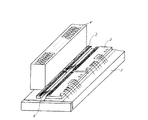
図5はかかる従来の電子写真方式プリンタの光源であるLEDヘッドの斜視図である。
【0004】
図5において、LEDヘッドは、基板1上に複数のLEDアレイチップ2を一列に配置し、これらの各LEDアレイは、複数の駆動用ドライバIC3よりなる回路とボンディングワイヤ4などで接続され、一直線上に配列したLEDプリントヘッドを構成する。
【0005】
そこで、所定の駆動信号に応じてLEDプリントヘッドのLEDアレイは発光し、発光した光は集束性ロッドレンズアレイ4´を経て、帯電した記録媒体(例えば感光ドラム)の表面を照射し、静電潜像を形成する。
【0006】
一方、ドラム上に形成された静電潜像は、感光ドラムの回転により現像器に送られ、静電潜像部にトナーが付着し現像され、転写器により用紙へ転写され印字が行われる。
【0007】
【発明が解決しようとする課題】
しかしながら、上記した従来のLEDアレイでは、以下のような問題点がある。
【0008】
図6は電子写真方式プリンタの光源であるLEDヘッドのLEDチップとLEDチップ間の隙間を示す図である。
【0009】
まず、第1に、超高精細化対応の印字ヘッドを作製する場合に、図6(a)に示すように、LEDチップ5とLEDチップ6間のつなぎ目7Aに、正規の間隙LN がある場合は良いが、図6(b)に示すように、LEDチップ5とLEDチップ6間のつなぎ目7Bに、正規の隙間以上の隙間LA (異常LA )が発生すると、印字時に印字ムラとなりやすいという問題点がある。
【0010】
この原因は、ウエハ・プロセスを終了し、後工程でウエハを切断し、チップに分割するときの切断ずれ、チップをプリント基板上に組み立てるときの組み立てずれなどによる。
【0011】
図示は省略するが、この逆、つまりLEDチップとLEDチップ間のつなぎ目の間隙が、正規の隙間以下の隙間となる場合もある。
【0012】
LEDチップが異常に配列された場合は、つなぎ目に隙間が生じ、その隙間領域は印字されないため、印字品質が低下する。
【0013】
第2に、各LEDチップごとに駆動用ドライバICを用いるため、駆動用ドライバICの使用量が大となり、コスト高になりやすいなどの問題点があった。
【0014】
本発明は、上記問題点を除去し、つなぎめの無い高品質印字ができ、かつ駆動用ドライバICの数を低減し、コストダウンを図ることができる一次元配列有機EL発光素子アレイヘッド及びその製造方法を提供することにある。
【0015】
【課題を解決するための手段】
本発明は、上記目的を達成するために、
(1)一次元配列有機EL発光素子アレイヘッドにおいて、絶縁性基板と、この絶縁性基板上に整流特性を有する有機EL材料を発光層に用い、各々分離されて形成された複数の発光素子からなる一次元配列発光素子アレイと、前記複数の発光素子を隣り合うn個の発光素子毎にm個に分けた各々をブロックと呼ぶとき、同一ブロックに含まれる発光素子に共通に接続されるブロック電極と、前記絶縁性基板と接して形成されたn個の下層配線と、この下層配線の上部に形成された層間絶縁膜と、該層間絶縁膜の上部に形成され一端が前記発光素子の各々と接続され他端が前記下層配線と前記層間絶縁膜に設けられたコンタクト穴を介し同一の前記ブロックに含まれる発光素子同士が互いに電気的に接続されないよう接続されるm×n個の上層配線とからなるマトリクス配線と、前記マトリクス配線の下層配線の各々と接続されたn個の個別信号電極と、前記ブロック電極に接続される第1の外部駆動回路と、前記個別信号電極に接続される第2の外部駆動回路とを備え、前記マトリクス配線の上層配線は、前記発光素子の下部に接続され、前記ブロック電極と前記個別信号電極との組み合わせにより前記複数の発光素子を選択的に発光させるようにしたものである。
【0016】
(2)上記(1)記載の一次元配列有機EL発光素子アレイヘッドにおいて、前記絶縁性基板上に形成される発光素子は、非透光性金属膜よりなる下部電極と、発光層と、ITO膜よりなる透明電極で形成される上部電極であるブロック電極から構成されるようにしたものである。
【0017】
(3)上記(1)記載の一次元配列有機EL発光素子アレイヘッドにおいて、前記ブロック電極にはグランドの電位よりなる信号(VL )を印加し、前記個別信号電極にはプラスの電位のパルス(VH )を印加し、発光素子を選択的に駆動するようにしたものである。
【0018】
(4)一次元配列有機EL発光素子アレイヘッドの製造方法において、絶縁性基板(100)上に多層配線の下層配線(111〜113)を形成する工程と、層間絶縁膜(120)を形成し、この層間絶縁膜(120)にコンタクト穴(131〜139)を形成する工程と、個別信号電極とその一部が発光層の下部電極(151〜159)を兼ねる多層配線の上層配線(141〜149)を形成し、前記コンタクト穴(131〜139)及び前記上層配線(141〜149)を通じて前記発光層の下部電極(151〜159)と前記下層配線(111〜113)とを接続する工程と、整流特性を有する有機EL材料を用いた一次元配列発光層(161〜169)を形成する工程と、ブロック信号用外部接続端子を有する発光層の上部電極となるブロック電極(171〜173)を形成する工程とを施すようにしたものである。
【0019】
(5)上記(4)記載の一次元配列有機EL発光素子アレイヘッドの製造方法において、n個の個別信号電極を有するm×nのマトリックス配線を形成した後、発光素子に接続されるm個のブロック電極を形成し、前記ブロック電極には第1の外部駆動回路を接続し、前記個別信号電極には第2の外部駆動回路とを接続するようにしたものである。
【0020】
(6)一次元配列有機EL発光素子アレイヘッドの製造方法において、絶縁性基板上に発光素子の下部電極及び個別信号電極となるマトリックス配線の下層配線(241〜249)を形成する工程と、層間絶縁膜(220)を形成し、この層間絶縁膜にコンタクト穴(231〜239)を形成する工程と、多層配線の上層配線(211〜213)を形成し、前記コンタクト穴(231〜239)及び前記下層配線(241〜249)を通じて、発光層の下部電極(251〜259)とマトリックス配線の上層配線(211〜213)及び個別信号電極(281〜283)とを接続する工程と、整流特性を有する有機EL材料を用いた一次元配列発光層(261〜269)を形成する工程と、ブロック信号用外部接続端子を有する発光層の上部電極となるブロック電極(271〜273)を形成する工程とを施すようにしたものである。
【0021】
(7)上記(6)記載の一次元配列有機EL発光素子アレイヘッドの製造方法において、n個の個別信号電極を有するm×nのマトリックス配線を形成した後、発光素子に接続されるm個のブロック電極を形成し、前記ブロック電極には第1の外部駆動回路を接続し、前記個別信号電極には第2の外部駆動回路とを接続するようにしたものである。
【0022】
【作用】
上記のように、絶縁性基板上に、整流特性を有する有機EL材料を発光層に用いた一次元配列発光素子アレイと、m個のブロック電極とn個の個別信号電極よりなるm×nのマトリックス電極で構成し、マトリックス駆動させることで、一次元に配列した有機EL発光素子アレイヘッドを作製し、電子写真方式プリンタの光源とするようにした。
【0023】
そして、耐熱性の低い有機EL発光材料を用いた発光素子のマトリックス配線駆動を行うため、マトリックス配線を先に行い、その後、発光素子の作製を行っている。
【0024】
【実施例】
以下、本発明の実施例を図面を参照しながら説明する。
【0025】
図1は本発明の第1実施例を示す一次元配列有機EL発光素子アレイヘッドの平面図、図2は図1のA−A線断面図、図3はその一次元配列有機EL発光素子アレイの等価回路図、図4はその一次元配列有機EL発光素子アレイの駆動タイミングチャートである。
【0026】
ここでは、総ドット数が9ドットの一次元配列発光素子アレイヘッド(3×3マトリックス駆動)を示している。
【0027】
まず、一次元配列発光素子アレイヘッドの製造方法を図1及び図2を用いて、説明する。
【0028】
詳細な説明の前に、有機EL材料の耐熱性について説明する。
【0029】
有機EL材料は、非結晶性の薄膜(300〜10000Å)であり、耐熱性が低いという膜固有の特性を有している。200℃以上になると結晶化が急激に進行し、発光特性、整流性が劣化するという問題点がある。このように、耐熱性が低いため、プロセス最高温度は200℃以下に抑えなければならない。
【0030】
マトリックス配線では、層間絶縁性が重要であるが、大面積にわたって十分な絶縁性を有する低温絶縁膜の形成技術はない。
【0031】
従って、有機EL材料を用いた素子でデバイスを作製し、マトリックス配線を行うためには、プロセス上の工夫が必要となる。
【0032】
以下、詳細に説明する。
【0033】
まず、ガラス、石英等の絶縁性基板100上に、Al,Cr,Ni,NiCr,W,Taなどの中から、少なくとも1種類の金属膜を真空蒸着法またはスパッタ法で形成した後、所定の条件でホトリソ・エッチングすることにより、多層配線の下層配線111〜113を形成する。
【0034】
そして、150〜200℃程度の低温プラズマCVD法により、Si3 N4 膜、SiO2 膜、SiON膜等からなる層間絶縁膜120を形成し、所定の条件でホトリソ・エッチングすることにより、層間絶縁膜120にコンタクト穴131〜139を形成する。
【0035】
次に、Li,Al,Mg,Mg−Ag,Al−Li,In等から、少なくとも一種類の非透明性金属膜を真空蒸着、共蒸着法により形成し、所定の条件でホトリソ・エッチングすることにより、多層配線の上層配線141〜149と、発光層の下部電極151〜159も同時に形成する。
【0036】
この時、多層配線の上層配線144〜146は、マトリックス配線の個別信号用外部接続端子181〜183にもなる。
【0037】
また、コンタクト穴131〜139及び多層配線の上層配線141〜149を通じて、発光層の下部電極151〜159と多層配線の下層配線111〜113は接続されている。
【0038】
次に、整流特性を有する有機EL材料を用いた一次元配列発光層161〜169を、真空蒸着法及び所定の条件でホトリソ・エッチングすることにより形成する。
【0039】
ここで、形成される発光体(発光層)は、2層型でも3層型でもよい。
【0040】
その2層型には、上層がホール輸送層/下層が発光層;電子輸送層のタイプと、上層が発光層;ホール輸送層/下層が電子輸送層のタイプがある。
【0041】
また、3層型は、上層がホール輸送層/中層が発光層/下層が電子輸送層となっている。
【0042】
蒸着される有機EL材料としては、電子輸送層としては、アルミキノリノール醋体(Alq3 )、オキサジアゾール誘導体、ホール輸送層としては、トリフェニルアミン誘導体、ポリビニールカルバゾールなどがある。
【0043】
発光層としては、トリフェニルジアミン、ペリレン誘導体、チアジゾール誘導体、スチルベンゼン誘導体などがある。
【0044】
そして、ITO膜を真空蒸着法またはスパッタ法で形成し、所定の条件でホトリソ・エッチングすることにより、ブロック電極171〜173を形成する。このブロック電極171〜173は、ブロック信号用外部接続端子を有する。
【0045】
9個の発光層(発光素子)161〜169は、上述の上部電極であるブロック電極171〜173、有機EL材料の発光層160、下部電極151〜159から構成されることになる。
【0046】
この実施例では、便宜上、3ドット×3ブロックの3×3マトリックス駆動の一次元配列有機EL発光素子アレイヘッドの製造方法について説明したが、当然マトリックス規模を128ドット×81ブロックなどに拡大することで、印字サイズ幅がA4(297mm)で、ドット数10368の1200dpiの一次元配列有機EL発光素子アレイヘッドとなる。
【0047】
完成した一次元配列有機EL発光素子アレイヘッドは、ブロック信号用外部接続端子(ブロック電極)171〜173と、個別信号用外部接続端子181〜183を通じて外部駆動回路に接続される。すなわち、ブロック信号用外部接続端子(ブロック電極)171〜173は、外部駆動回路であるドライバIC191へ、個別信号用外部接続端子181〜183は外部駆動回路であるドライバIC192へと接続されている。
【0048】
発光層(発光素子)161〜169の電気光学特性(電圧−輝度)によれば、順方向+3〜10Vの低い印加電圧で、3000〜7000cd/m2 の十分な発光強度を有している。
【0049】
また、発光層(発光素子)161〜169の電気特性(電圧−電流)によれば、順方向電圧+3〜10V印加の場合、100〜200mA/cm2 、逆方向電圧に対するリーク電流は微小であり、逆耐圧は−15〜−20Vと十分な整流特性を有している。
【0050】
本発明の第1実施例の一次元配列有機EL発光素子アレイヘッド駆動方法について図3及び図4を参照して説明する。
【0051】
外部駆動回路より、個別信号用外部接続端子181〜183とブロック電極171〜173には、プラスの電位(VH )、グランドの電位(VL )の2種類の電位よりなる制御信号パルス、つまり、ブロック制御信号、個別電極信号が印加される。
【0052】
また、プラスの電位VH は順方向+3〜10Vであり、発光層(発光素子)は電流100〜200mA/cm2 、発光強度3000〜7000cd/m2 の特性を有する。
【0053】
更に、グランドの電位VL は0Vであり、発光層(発光素子)は電流0mA/cm2 、発光強度3000〜7000cd/m2 の特性を有する。
【0054】
図4に示すように、1ライン周期TL ごとに、ブロック周期TB にあわせてブロック制御信号を順次切替え、切替えと同期させながら個別信号を個別信号用外部接続端子(個別信号電極)181〜183に印加することにより、選択的に任意のドットを発光時間tで発光させることができる。
【0055】
すなわち、ブロック電極171〜173には、グランドの電位よりなる信号(VL )を印加し、個別信号用外部接続端子(個別信号電極)181〜183には、プラスの電位のパルス(VH )を印加することで選択的に駆動することができる。
【0056】
以上述べた一次元配列有機EL発光素子アレイは、ドライバIC191,192よりなる外部駆動回路と接続され、一直線上に配列したプリントヘッドを構成する。
【0057】
図4に示すような所定の駆動信号に応じて、一次元配列有機EL発光素子アレイを発光させ、発光した光は集束性ロッドレンズアレイを経て帯電した記録媒体(例えば、感光ドラム)の表面を照射し、静電潜像を形成する。
【0058】
ドラム上に形成された静電潜像は、感光ドラムの回転により現像器に送られ、静電潜像部にトナーが付着し現像され、転写器により用紙へ転写され印字が行われる。
【0059】
次に、本発明の第2実施例を図面を参照しながら説明する。
【0060】
ここでも、総ドット数が9ドットの一次元配列発光素子アレイヘッド(3×3マトリックス駆動)を図7〜図10に示す。
【0061】
図7は本発明の第2実施例を示す一次元配列発光素子アレイヘッドの平面図、図8はその一次元配列発光素子アレイヘッドのB−B線断面図、図9はその一次元配列有機EL発光素子アレイの等価回路図、図10はその一次元配列有機EL発光素子アレイの駆動タイミングチャートである。
【0062】
まず、ガラス、石英などの絶縁性基板200上に、ITO膜を真空蒸着法、またはスパッタ法で形成し、所定の条件でホトリソ・エッチングすることにより、マトリックス配線の下層配線241〜249を形成する。
【0063】
このマトリックス配線の下層配線241〜249は、発光層の下部電極251〜259も兼ねている。また、244〜246はマトリックス配線の個別信号用外部接続端子281〜283を有している。
【0064】
そして、150〜200℃程度の低温プラズマCVD法により、Si3 N4 膜、SiO2 膜、SiON膜などからなる層間絶縁膜220を形成し、所定の条件でホトリソ・エッチングすることで、層間絶縁膜220にコンタクト穴231〜239を形成する。
【0065】
次に、Al,Cr,Ni,NiCr,W,Ta,Moなどの中から、少なくとも一種類の金属膜を真空蒸着法、またはスパッタ法で形成した後、所定の条件でホトリソ・エッチングすることで、多層配線の上層配線211〜213を形成する。
【0066】
また、コンタクト穴231〜239及び多層配線(マトリックス配線)の下層配線241〜249を通じて、発光層の下部電極251〜259と多層配線(マトリックス配線)の上層配線211〜213、そして、個別信号用外部接続端子281〜283を有している。
【0067】
次に、整流特性を有する有機EL材料からなる一次元配列の発光層260に用いた一次元配列発光層261〜269を、真空蒸着法及び所定の条件でホトリソ・エッチングすることで形成する。
【0068】
次に、Li,Al,Mg,Mg−Ag,Al−Li,Inなどから少なくとも一種類の非透明性金属膜を真空蒸着、共蒸着法により形成し、所定の条件でホトリソ・エッチングすることで、発光層の上部電極としてのブロック電極271〜273を形成する。
【0069】
この電極271〜273は、ブロック電極でありブロック信号用外部接続端子を有している。
【0070】
9個の発光層(発光素子)261〜269は、上述の上部電極であるブロック電極271〜273、有機EL材料の一次元配列の発光層260、発光層の下部電極251〜259から構成されることになる。
【0071】
実施例では、便宜上、3ドット×3ブロックの3×3マトリックス駆動の一次元配列有機EL発光素子アレイヘッドの製造方法について説明したが、当然マトリックス規模を128ドット×81ブロックなどに拡大することで、印字サイズ幅がA4(297mm)で、ドット数10368の1200dpiの一次元配列有機EL発光素子アレイヘッドとなる。
【0072】
完成した一次元配列有機EL発光素子アレイヘッドは、ブロック電極(ブロック信号用外部接続端子)271〜273と個別信号用外部接続端子281〜283を通じて外部駆動回路としてのドライバIC291とドライバIC292に接続される。
【0073】
また、発光層(発光素子)261〜269の電気光学特性(電圧−輝度)によれば、順方向+3〜10Vの低い印加電圧で、3000〜7000cd/m2 の十分な発光強度を有している。
【0074】
また、発光層(発光素子)261〜269の電気特性(電圧−電流)によれば、順方向電圧+3〜10V印加で100〜200mA/cm2 、逆方向電圧に対するリーク電流は微小であり、逆耐圧は−15〜−20Vと十分な整流特性を有している。
【0075】
本発明の一次元配列有機EL発光素子アレイヘッドの動作を図9及び図10を用いて説明する。
【0076】
図9に示すように、外部駆動回路より、個別信号用外部接続端子281〜283とブロック電極271〜273には、プラスの電位(VH )、グランドの電位(VL )の2種類の電位よりなる制御信号パルス、つまり、ブロック制御信号、個別電極信号が印加される。
【0077】
また、プラスの電位VH は順方向+3〜10Vであり、発光層(発光素子)は電流100〜200mA/cm2 、発光強度3000〜7000cd/m2 の特性を有する。
【0078】
更に、グランドの電位VL は0Vであり、発光層(発光素子)は電流0mA/cm2 、発光強度3000〜7000cd/m2 の特性を有する。
【0079】
図10に示すように、1ライン周期TL ごとに、ブロック周期TB にあわせてブロック制御信号を順次切替え、切替えと同期させながら個別信号を個別信号用外部接続端子(個別信号電極)281〜283に印加することにより、選択的に任意のドットを発光時間tで発光させることができる。
【0080】
すなわち、ブロック電極271〜273には、プラスの電位よりなる信号(VH )を印加し、個別信号用外部接続端子(個別信号電極)281〜283には、グランドの電位よりなる信号(VL )を印加することで選択的に駆動することができる。
【0081】
以上述べた一次元配列有機EL発光素子アレイは、ドライバIC291,292(図7参照)よりなる外部駆動回路と接続され、一直線上に配列したプリントヘッドを構成する。
【0082】
なお、本発明は上記実施例に限定されるものではなく、本発明の趣旨に基づいて種々の変形が可能であり、これらを本発明の範囲から排除するものではない。
【0083】
【発明の効果】
以上、詳細に説明したように、本発明によれば、以下のような効果を奏することができる。
【0084】
本発明によれば、有機EL材料を用いた発光素子をマトリックス配線駆動させるために、発光素子作製前にマトリックス配線を形成するというプロセス上の工夫を行い、長尺の絶縁性基板上に一次元的に有機EL発光素子を配列しているため、チップ間の切れ目が無い、つまり印字上つなぎ目の無い高印字品質ができる。
【0085】
また、十分な整流特性を保持した有機EL発光素子を、マトリックス配線の信号逆流阻止のブロッキングダイオードとしても使用していることで、マトリックス駆動しているため、駆動用ドライバICの数を低減でき、コストダウンを図ることができる。
【0086】
更に、駆動用ドライバICの数を低減できるため、ワイヤボンドなどの実装コストを大幅に低減できるため、二重にコストダウンとなる。
【図面の簡単な説明】
【図1】 本発明の第1実施例を示す一次元配列有機EL発光素子アレイヘッドの平面図である。
【図2】 図1のA−A線断面図である。
【図3】 本発明の第1実施例を示す一次元配列有機EL発光素子アレイの等価回路図である。
【図4】 本発明の第1実施例を示す一次元配列有機EL発光素子アレイの駆動タイミングチャートである。
【図5】 従来の電子写真方式プリンタの光源であるLEDヘッドの斜視図である。
【図6】 電子写真方式プリンタの光源であるLEDヘッドのLEDチップとLEDチップ間の隙間を示す図である。
【図7】 本発明の第2実施例を示す一次元配列発光素子アレイヘッドの平面図である。
【図8】 本発明の第2実施例を示す一次元配列発光素子アレイヘッドのB−B線断面図である。
【図9】 本発明の第2実施例を示す一次元配列有機EL発光素子アレイの等価回路図である。
【図10】 本発明の第2実施例を示す一次元配列有機EL発光素子アレイの駆動タイミングチャートである。
【符号の説明】
100,200 絶縁性基板
111〜113,241〜249 多層配線の下層配線
120,220 層間絶縁膜
131〜139,231〜239 コンタクト穴
141〜149,211〜213 多層配線の上層配線
151〜159,251〜259 発光層の下部電極
181〜183,281〜283 個別信号用外部接続端子(個別信号電極)
160,161〜169,260,261〜269 発光層(発光素子)
171〜173,271〜273 ブロック電極
191,192,291,292 ドライバIC[0001]
[Industrial application fields]
The present invention relates to a one-dimensional array organic EL light emitting element array head used for an organic EL (electroluminescence) printer head which is a light source of an electrophotographic printer, and a manufacturing method thereof.
[0002]
[Prior art]
Conventionally, as the technology in such a field, for example, there are the following.
[0003]
FIG. 5 is a perspective view of an LED head which is a light source of such a conventional electrophotographic printer.
[0004]
In FIG. 5, the LED head has a plurality of LED array chips 2 arranged in a row on a substrate 1, and each LED array is connected to a circuit comprising a plurality of
[0005]
Therefore, the LED array of the LED print head emits light in response to a predetermined drive signal, emitted light through a focusing rod lens array 4 ', irradiating the charged surface of the recording medium (for example, a photosensitive drum), electrostatic A latent image is formed.
[0006]
On the other hand, the electrostatic latent image formed on the drum is sent to the developing device by the rotation of the photosensitive drum, the toner adheres to the electrostatic latent image portion and is developed, transferred to the paper by the transfer device, and printing is performed.
[0007]
[Problems to be solved by the invention]
However, the conventional LED array described above has the following problems.
[0008]
FIG. 6 is a view showing a gap between the LED chips of the LED head which is a light source of the electrophotographic printer.
[0009]
First, when producing a print head compatible with ultra-high definition, there is a regular gap L N at the joint 7A between the LED chip 5 and the
[0010]
The cause of this is due to a deviation in cutting when the wafer process is completed and the wafer is cut and divided into chips in a subsequent process, an assembly deviation in assembling the chip on the printed circuit board, and the like.
[0011]
Although not shown in the drawings, the opposite, that is, the gap between the LED chip and the LED chip may be a gap that is less than or equal to the regular gap.
[0012]
When the LED chips are abnormally arranged, a gap is formed at the joint, and the gap area is not printed, so that the print quality is deteriorated.
[0013]
Secondly, since a driver IC is used for each LED chip, there is a problem that the amount of the driver driver IC used is large and the cost is likely to increase.
[0014]
The present invention eliminates the above-mentioned problems, enables high-quality printing without splicing, reduces the number of driver ICs for driving, and can reduce costs, and its head It is to provide a manufacturing method.
[0015]
[Means for Solving the Problems]
In order to achieve the above object, the present invention provides
(1) In a one-dimensional array organic EL light emitting device array head, an insulating substrate and an organic EL material having a rectifying characteristic on the insulating substrate are used as a light emitting layer, and a plurality of light emitting devices formed separately from each other. a one-dimensional array light emitting device array comprising, when referred to as the plurality of light emitting elements adjacent the n blocks each divided into m pieces to each light emitting element, lube are connected in common to the light-emitting elements included in the same block A lock electrode, n lower layer wirings formed in contact with the insulating substrate, an interlayer insulating film formed on the lower layer wiring , and one end of the light emitting element formed on the interlayer insulating film . on the other end is connected to each of the m × n light emitting elements are connected to each other so as not to be electrically connected to each other included in the same said block through a contact hole formed in the interlayer insulating film and the lower layer wiring A matrix wiring made of the wiring, and the n individual signal electrode connected with each of the lower layer wiring of the matrix wiring, a first external drive circuit connected to said block electrode, connected to said individual signal electrodes second and an external drive circuit that, the upper layer wiring of the matrix wiring is connected to a lower portion of the light emitting element, selectively emitting the plurality of light emitting elements by the combination of the individual signal electrodes and said block electrodes It is made to let you.
[0016]
(2) In the one-dimensional array organic EL light emitting element array head described in (1) above, the light emitting element formed on the insulating substrate includes a lower electrode made of a non-translucent metal film, a light emitting layer, ITO The block electrode is an upper electrode formed of a transparent electrode made of a film.
[0017]
(3) In the one-dimensional array organic EL light emitting device array head described in (1) above, a signal (V L ) composed of a ground potential is applied to the block electrode, and a pulse having a positive potential is applied to the individual signal electrode. The light emitting element is selectively driven by applying (V H ).
[0018]
(4) In the method for manufacturing a one-dimensional array organic EL light emitting device array head, a step of forming a lower layer wiring (111 to 113) of a multilayer wiring on an insulating substrate (100) and an interlayer insulating film (120) are formed. The step of forming contact holes (131 to 139) in the interlayer insulating film (120), and the upper layer wiring (141 to 141) of the multilayer wiring in which the individual signal electrode and a part thereof also serve as the lower electrodes (151 to 159) of the light emitting layer 149) is formed, a step of connecting said lower electrode (151 to 159) and the lower wiring of the light emitting layer (111 to 113) through the contact hole (131-139) and the upper wiring (141-149) , forming a one-dimensional array light emitting layer using an organic EL material (161-169) having a rectifying characteristic, and the upper portion electrode of the light emitting layer having an external connection terminal block signal I It is obtained by so applying and forming a block electrode (171-173).
[0019]
(5) In the manufacturing method of the one-dimensionally arranged organic EL light emitting element array head described in (4) above, after forming m × n matrix wirings having n individual signal electrodes, m pieces connected to the light emitting elements These block electrodes are formed, a first external drive circuit is connected to the block electrodes, and a second external drive circuit is connected to the individual signal electrodes.
[0020]
( 6 ) In the method for manufacturing a one-dimensionally arranged organic EL light emitting element array head, a step of forming lower layer wirings (241 to 249) of matrix wirings to be the lower electrodes of the light emitting elements and the individual signal electrodes on the insulating substrate; Forming an insulating film (220) and forming contact holes (231 to 239) in the interlayer insulating film; and forming upper layer wirings (211 to 213) of the multilayer wiring; and the contact holes (231 to 239) and through the lower wiring (241 to 249), a step of connecting the lower electrode (251 to 259) and upper-layer wiring of the matrix wiring of the light emitting layer (211 to 213) and the individual signal electrodes (281-283), the rectifying characteristics A step of forming a one-dimensional array light emitting layer (261-269) using an organic EL material, and a light emitting layer having a block signal external connection terminal It is obtained by so applying and forming a block electrode (271 to 273) serving as an electrode.
[0021]
( 7 ) In the manufacturing method of the one-dimensionally arranged organic EL light emitting element array head described in ( 6 ) above, after forming m × n matrix wirings having n individual signal electrodes, m pieces connected to the light emitting elements These block electrodes are formed, a first external drive circuit is connected to the block electrodes, and a second external drive circuit is connected to the individual signal electrodes.
[0022]
[Action]
As described above, an mxn array of a one-dimensional array light emitting element array using an organic EL material having a rectifying characteristic as a light emitting layer on an insulating substrate, m block electrodes, and n individual signal electrodes. An organic EL light-emitting element array head arranged in a one-dimensional manner was fabricated by matrix drive and matrix driving, and used as a light source for an electrophotographic printer.
[0023]
And in order to perform matrix wiring drive of the light emitting element using organic electroluminescent light emitting material with low heat resistance, matrix wiring is performed first and the light emitting element is produced after that.
[0024]
【Example】
Embodiments of the present invention will be described below with reference to the drawings.
[0025]
FIG. 1 is a plan view of a one-dimensional array organic EL light-emitting element array head showing a first embodiment of the present invention, FIG. 2 is a cross-sectional view taken along line AA of FIG. 1, and FIG. FIG. 4 is a drive timing chart of the one-dimensional array organic EL light emitting element array.
[0026]
Here, a one-dimensional array light emitting element array head (3 × 3 matrix drive) having a total dot number of 9 dots is shown.
[0027]
First, a method for manufacturing a one-dimensional array light emitting element array head will be described with reference to FIGS.
[0028]
Prior to the detailed description, the heat resistance of the organic EL material will be described.
[0029]
The organic EL material is a non-crystalline thin film (300 to 10,000 mm) and has film-specific characteristics such as low heat resistance. At 200 ° C. or higher, there is a problem that crystallization rapidly proceeds and the light emission characteristics and rectification properties deteriorate. Thus, since heat resistance is low, the maximum process temperature must be suppressed to 200 ° C. or lower.
[0030]
In matrix wiring, interlayer insulation is important, but there is no technique for forming a low-temperature insulating film having sufficient insulation over a large area.
[0031]
Therefore, in order to manufacture a device with an element using an organic EL material and perform matrix wiring, a device on the process is required.
[0032]
This will be described in detail below.
[0033]
First, at least one type of metal film is formed on an insulating
[0034]
Then, an
[0035]
Next, at least one non-transparent metal film is formed from Li, Al, Mg, Mg—Ag, Al—Li, In, or the like by vacuum deposition or co-evaporation, and photolithography and etching is performed under predetermined conditions. Thus, the upper wirings 141 to 149 of the multilayer wiring and the
[0036]
At this time, the upper wirings 144 to 146 of the multilayer wiring also become the individual signal
[0037]
The
[0038]
Next, one-dimensionally arranged light emitting
[0039]
Here, the light-emitting body (light-emitting layer) to be formed may be a two-layer type or a three-layer type.
[0040]
The two-layer type includes a hole transport layer / lower layer as a light emitting layer; an electron transport layer type, and an upper layer as a light emitting layer; a hole transport layer / lower layer as an electron transport layer type.
[0041]
In the three-layer type, the upper layer is a hole transport layer / middle layer is a light emitting layer / lower layer is an electron transport layer.
[0042]
Examples of the organic EL material to be deposited include an aluminum quinolinol housing (Alq 3 ) and an oxadiazole derivative as an electron transport layer, and a triphenylamine derivative and polyvinyl carbazole as a hole transport layer.
[0043]
Examples of the light emitting layer include triphenyldiamine, perylene derivatives, thiadizole derivatives, and stilbene derivatives.
[0044]
Then, an ITO film is formed by vacuum deposition or sputtering, and photolithography / etching is performed under predetermined conditions, thereby forming
[0045]
The nine light emitting layers (light emitting elements) 161 to 169 are composed of the
[0046]
In this embodiment, the manufacturing method of the one-dimensional array organic EL light-emitting element array head of 3 × 3 matrix driving of 3 dots × 3 blocks has been described for convenience. Naturally, the matrix scale should be expanded to 128 dots × 81 blocks or the like. Thus, the print size width is A4 (297 mm) and the number of dots is 10368, which is a 1200 dpi one-dimensional array organic EL light emitting element array head.
[0047]
The completed one-dimensional array organic EL light emitting element array head is connected to an external drive circuit through block signal external connection terminals (block electrodes) 171 to 173 and individual signal
[0048]
According to the electro-optical characteristics (voltage-luminance) of the light-emitting layers (light-emitting elements) 161 to 169, it has a sufficient light emission intensity of 3000 to 7000 cd / m 2 at a low applied voltage of +3 to 10 V in the forward direction.
[0049]
Further, according to the electrical characteristics (voltage-current) of the light emitting layers (light emitting elements) 161 to 169, when a forward voltage of +3 to 10 V is applied, 100 to 200 mA / cm 2 , and a leakage current with respect to a reverse voltage is very small. The reverse breakdown voltage is -15 to -20V and has sufficient rectification characteristics.
[0050]
A method of driving the one-dimensional array organic EL light emitting element array head according to the first embodiment of the present invention will be described with reference to FIGS.
[0051]
From the external drive circuit, the individual signal
[0052]
The positive potential V H is +3 to 10 V in the forward direction, and the light emitting layer (light emitting element) has characteristics of a current of 100 to 200 mA / cm 2 and a light emission intensity of 3000 to 7000 cd / m 2 .
[0053]
Further, the ground potential V L is 0 V, and the light emitting layer (light emitting element) has characteristics of a current of 0 mA / cm 2 and a light emission intensity of 3000 to 7000 cd / m 2 .
[0054]
As shown in FIG. 4, 1 in every line period T L, sequentially switching the block control signals in accordance with the block period T B, switched while synchronizing individual signal discrete signal external connection terminal (an individual signal electrodes) 181~ By applying the voltage to H.sub.183, it is possible to selectively emit an arbitrary dot with a light emission time t.
[0055]
That is, a signal (V L ) having a ground potential is applied to the
[0056]
The one-dimensional array organic EL light emitting element array described above is connected to an external drive circuit composed of
[0057]
In response to a predetermined drive signal as shown in FIG. 4, the one-dimensional array organic EL light emitting element array emits light, and the emitted light passes through the surface of a recording medium (for example, a photosensitive drum) charged through a converging rod lens array. Irradiate to form an electrostatic latent image.
[0058]
The electrostatic latent image formed on the drum is sent to the developing device by the rotation of the photosensitive drum, and the toner adheres to the electrostatic latent image portion and is developed. The toner is transferred to the paper by the transfer device, and printing is performed.
[0059]
Next, a second embodiment of the present invention will be described with reference to the drawings.
[0060]
Here, a one-dimensional array light emitting element array head (3 × 3 matrix drive) having a total dot number of 9 dots is shown in FIGS.
[0061]
FIG. 7 is a plan view of a one-dimensional array light-emitting element array head showing a second embodiment of the present invention, FIG. 8 is a cross-sectional view of the one-dimensional array light-emitting element array head taken along line BB, and FIG. An equivalent circuit diagram of the EL light emitting element array, FIG. 10 is a drive timing chart of the one-dimensional array organic EL light emitting element array.
[0062]
First, an ITO film is formed on an insulating
[0063]
The lower layer wirings 241 to 249 of the matrix wiring also serve as the
[0064]
Then, an
[0065]
Next, at least one type of metal film is formed by vacuum deposition or sputtering from Al, Cr, Ni, NiCr, W, Ta, Mo, etc., and then photolithography etching is performed under predetermined conditions. Then, the upper wirings 211 to 213 of the multilayer wiring are formed.
[0066]
Further, through the contact holes 231 to 239 and the lower layer wirings 241 to 249 of the multilayer wiring (matrix wiring), the
[0067]
Next, the one-dimensional array light-emitting
[0068]
Next, by forming at least one non-transparent metal film from Li, Al, Mg, Mg—Ag, Al—Li, In, etc. by vacuum deposition or co-evaporation, and performing photolithography etching under predetermined conditions. Then, block
[0069]
These
[0070]
The nine light emitting layers (light emitting elements) 261 to 269 are configured by the
[0071]
In the embodiment, the manufacturing method of the one-dimensional array organic EL light emitting element array head driven by 3 × 3 matrix of 3 dots × 3 blocks has been described for convenience, but naturally the matrix scale is expanded to 128 dots × 81 blocks or the like. The print size width is A4 (297 mm), and a 1200-dpi one-dimensional array organic EL light-emitting element array head with 10368 dots is obtained.
[0072]
The completed one-dimensional array organic EL light emitting element array head is connected to a
[0073]
Further, according to the electro-optical characteristics (voltage-luminance) of the light-emitting layers (light-emitting elements) 261 to 269, the light-emitting layers (light-emitting elements) have a sufficient light emission intensity of 3000 to 7000 cd / m 2 at a low applied voltage of +3 to 10 V in the forward direction. Yes.
[0074]
Further, according to the electrical characteristics (voltage-current) of the light emitting layers (light emitting elements) 261 to 269, 100 to 200 mA / cm 2 when a forward voltage +3 to 10 V is applied, and a leakage current against a reverse voltage is very small. The withstand voltage has a sufficient rectifying characteristic of −15 to −20V.
[0075]
The operation of the one-dimensional array organic EL light emitting element array head of the present invention will be described with reference to FIGS.
[0076]
As shown in FIG. 9, from the external drive circuit, the individual signal
[0077]
The positive potential V H is +3 to 10 V in the forward direction, and the light emitting layer (light emitting element) has characteristics of a current of 100 to 200 mA / cm 2 and a light emission intensity of 3000 to 7000 cd / m 2 .
[0078]
Further, the ground potential V L is 0 V, and the light emitting layer (light emitting element) has characteristics of a current of 0 mA / cm 2 and a light emission intensity of 3000 to 7000 cd / m 2 .
[0079]
As shown in FIG. 10, 1 per line period T L, sequentially switching the block control signals in accordance with the block period T B, switched while synchronizing individual signal discrete signal external connection terminal (an individual signal electrodes) 281 to By applying the voltage to H.283, it is possible to selectively emit any dot with the light emission time t.
[0080]
That is, a signal (V H ) having a positive potential is applied to the
[0081]
The one-dimensional array organic EL light emitting element array described above is connected to an external drive circuit composed of
[0082]
In addition, this invention is not limited to the said Example, A various deformation | transformation is possible based on the meaning of this invention, and these are not excluded from the scope of the present invention.
[0083]
【The invention's effect】
As described above in detail, according to the present invention, the following effects can be obtained.
[0084]
According to the present invention, in order to drive a light emitting device using an organic EL material to drive a matrix wiring, a process ingenuity is formed such that a matrix wiring is formed before manufacturing the light emitting device, and a one-dimensional pattern is formed on a long insulating substrate. In addition, since organic EL light emitting elements are arranged in sequence, there is no break between chips, that is, high print quality without a joint on printing can be achieved.
[0085]
In addition, since the organic EL light-emitting element that retains sufficient rectification characteristics is also used as a blocking diode for blocking the signal backflow of the matrix wiring, because it is matrix driven, the number of driver ICs for driving can be reduced, Cost can be reduced.
[0086]
Furthermore, since the number of driver ICs for driving can be reduced, the mounting cost for wire bonding and the like can be greatly reduced, resulting in a double cost reduction.
[Brief description of the drawings]
FIG. 1 is a plan view of a one-dimensionally arranged organic EL light emitting element array head showing a first embodiment of the present invention.
FIG. 2 is a cross-sectional view taken along line AA in FIG.
FIG. 3 is an equivalent circuit diagram of a one-dimensional array organic EL light emitting element array showing a first embodiment of the present invention.
FIG. 4 is a drive timing chart of the one-dimensional array organic EL light emitting element array showing the first embodiment of the present invention.
FIG. 5 is a perspective view of an LED head that is a light source of a conventional electrophotographic printer.
FIG. 6 is a diagram showing a gap between LED chips of an LED head that is a light source of an electrophotographic printer.
FIG. 7 is a plan view of a one-dimensional array light emitting element array head showing a second embodiment of the present invention.
FIG. 8 is a sectional view taken along line BB of the one-dimensional array light emitting element array head according to the second embodiment of the present invention.
FIG. 9 is an equivalent circuit diagram of a one-dimensionally arranged organic EL light emitting element array showing a second embodiment of the present invention.
FIG. 10 is a drive timing chart of the one-dimensional array organic EL light emitting element array showing a second embodiment of the present invention.
[Explanation of symbols]
100, 200 Insulating substrate 111-113, 241-249 Multilayer wiring
160, 161-169, 260, 261-269 Light emitting layer (light emitting element)
171 to 173, 271 to 273 Block electrode 191,192,291,292 Driver IC
Claims (7)
(b)該絶縁性基板上に整流特性を有する有機EL材料を発光層に用い、各々分離されて形成された複数の発光素子からなる一次元配列発光素子アレイと、
(c)前記複数の発光素子を隣り合うn個の発光素子毎にm個に分けた各々をブロックと呼ぶとき、同一ブロックに含まれる発光素子に共通に接続されるブロック電極と、
(d)前記絶縁性基板と接して形成されたn個の下層配線と、該下層配線の上部に形成された層間絶縁膜と、該層間絶縁膜の上部に形成され一端が前記発光素子の各々と接続され他端が前記下層配線と前記層間絶縁膜に設けられたコンタクト穴を介し同一の前記ブロックに含まれる発光素子同士が互いに電気的に接続されないよう接続されるm×n個の上層配線とからなるマトリクス配線と、
(e)前記マトリクス配線の下層配線の各々と接続されたn個の個別信号電極と、
(f)前記ブロック電極に接続される第1の外部駆動回路と、
(g)前記個別信号電極に接続される第2の外部駆動回路とを備え、
(h)前記マトリクス配線の上層配線は、前記発光素子の下部に接続され、
(i)前記ブロック電極と前記個別信号電極との組み合わせにより前記複数の発光素子を選択的に発光させることを特徴とする一次元配列有機EL発光素子アレイヘッド。(A) an insulating substrate;
(B) a one-dimensional array light-emitting element array composed of a plurality of light-emitting elements each formed separately using an organic EL material having a rectifying characteristic on the insulating substrate for a light-emitting layer;
(C) when referred to as the plurality of light emitting elements adjacent the n blocks each divided into m pieces to each light emitting element, a lube locked electrode connected in common to light-emitting elements included in the same block,
(D) each of said insulating substrate and the n-number of the lower layer wiring formed in contact with, the lower layer and the interlayer insulating film formed over the wiring, one said light emitting element is formed on top of the interlayer insulating film connected the other end the lower layer wiring and the interlayer so that the light emitting element to each other included in the same said block through a contact hole provided in the insulating film is not electrically connected to each other connected by the m × n upper wiring and Matrix wiring consisting of
(E) the n individual signal electrode connected with each of the lower layer wiring of the matrix wiring,
(F) a first external drive circuit connected to the block electrode;
(G) a second external drive circuit connected to the individual signal electrode,
(H) The upper layer wiring of the matrix wiring is connected to the lower part of the light emitting element,
(I) A one-dimensional array organic EL light emitting element array head, wherein the plurality of light emitting elements are selectively caused to emit light by a combination of the block electrodes and the individual signal electrodes .
(b)層間絶縁膜を形成し、該層間絶縁膜にコンタクト穴を形成する工程と、
(c)個別信号電極とその一部が発光層の下部電極を兼ねる多層配線の上層配線を形成し、前記コンタクト穴及び前記上層配線を通じて前記発光層の下部電極と前記下層配線とを接続する工程と、
(d)整流特性を有する有機EL材料を用いた一次元配列発光層を形成する工程と、
(e)ブロック信号用外部接続端子を有する発光層の上部電極となるブロック電極を形成する工程とを施すことを特徴とする一次元配列有機EL発光素子アレイヘッドの製造方法。Forming a lower layer wiring of the multilayer wiring (a) an insulating substrate,
(B) forming an interlayer insulating film and forming a contact hole in the interlayer insulating film;
(C) a part of the individual signal electrodes to form an upper wiring of the multilayer wiring serving as a lower electrode of the light emitting layer, the contact holes and the step of connecting the lower layer wiring and the lower electrode of the light emitting layer through the upper wiring When,
(D) forming a one-dimensional array light emitting layer using an organic EL material having rectifying characteristics;
(E) a one-dimensional array organic EL device manufacturing method of the array head, characterized in that applying and forming a block electrode serving as the upper portion electrode of the light emitting layer having an external connection terminal block signal.
(b)層間絶縁膜を形成し、該層間絶縁膜にコンタクト穴を形成する工程と、
(c)多層配線の上層配線を形成し、前記コンタクト穴及び前記下層配線を通じて、発光層の下部電極とマトリックス配線の上層配線及び個別信号電極とを接続する工程と、
(d)整流特性を有する有機EL材料を用いた一次元配列発光層を形成する工程と、
(e)ブロック信号用外部接続端子を有する発光層の上部電極となるブロック電極を形成する工程とを施すことを特徴とする一次元配列有機EL発光素子アレイヘッドの製造方法。(A) forming a lower layer wiring of a matrix wiring to be a lower electrode of the light emitting element and an individual signal electrode on an insulating substrate;
(B) forming an interlayer insulating film and forming a contact hole in the interlayer insulating film;
And step (c) to form an upper wiring of the multilayer wiring, through the contact hole and the lower wiring, which connects the upper wiring and the individual signal electrodes of the lower electrode and the matrix wiring of the light emitting layer,
(D) forming a one-dimensional array light emitting layer using an organic EL material having rectifying characteristics;
(E) A method of manufacturing a one-dimensional arrayed organic EL light emitting element array head, comprising: a step of forming a block electrode serving as an upper electrode of a light emitting layer having a block signal external connection terminal.
Priority Applications (1)
| Application Number | Priority Date | Filing Date | Title |
|---|---|---|---|
| JP245695A JP3696276B2 (en) | 1995-01-11 | 1995-01-11 | One-dimensional array organic EL light-emitting element array head and manufacturing method thereof |
Applications Claiming Priority (1)
| Application Number | Priority Date | Filing Date | Title |
|---|---|---|---|
| JP245695A JP3696276B2 (en) | 1995-01-11 | 1995-01-11 | One-dimensional array organic EL light-emitting element array head and manufacturing method thereof |
Publications (2)
| Publication Number | Publication Date |
|---|---|
| JPH08187889A JPH08187889A (en) | 1996-07-23 |
| JP3696276B2 true JP3696276B2 (en) | 2005-09-14 |
Family
ID=11529807
Family Applications (1)
| Application Number | Title | Priority Date | Filing Date |
|---|---|---|---|
| JP245695A Expired - Lifetime JP3696276B2 (en) | 1995-01-11 | 1995-01-11 | One-dimensional array organic EL light-emitting element array head and manufacturing method thereof |
Country Status (1)
| Country | Link |
|---|---|
| JP (1) | JP3696276B2 (en) |
Families Citing this family (5)
| Publication number | Priority date | Publication date | Assignee | Title |
|---|---|---|---|---|
| JPH1044497A (en) | 1996-07-31 | 1998-02-17 | Canon Inc | Recording head |
| JP2001088345A (en) | 1999-09-20 | 2001-04-03 | Sanyo Electric Co Ltd | Optical printing head |
| CN1374906A (en) * | 1999-09-20 | 2002-10-16 | 三洋电机株式会社 | Driving IC and optical print head |
| US6606110B2 (en) * | 2000-12-27 | 2003-08-12 | Polaroid Corporation | Integral organic light emitting diode printhead |
| KR100795814B1 (en) * | 2007-01-09 | 2008-01-21 | 삼성에스디아이 주식회사 | Retardation film and organic light emitting device therewith |
-
1995
- 1995-01-11 JP JP245695A patent/JP3696276B2/en not_active Expired - Lifetime
Also Published As
| Publication number | Publication date |
|---|---|
| JPH08187889A (en) | 1996-07-23 |
Similar Documents
| Publication | Publication Date | Title |
|---|---|---|
| US6140766A (en) | Organic EL device | |
| EP0704915B1 (en) | Organic electroluminescent light-emitting array and optical head assembly | |
| JP4074099B2 (en) | Flat display device and manufacturing method thereof | |
| CN101093853B (en) | Organic light emitting diode display and method for manufacturing the same | |
| US8059067B2 (en) | Electroluminescent device, method for manufacturing electroluminescent device, and electronic apparatus | |
| JP2007219517A (en) | Organic light emitting device and manufacturing method of the same | |
| JP2004212996A (en) | Organic electroluminescent element and its manufacturing method | |
| JP2005327674A (en) | Organic electroluminescent display element, display device having the same, and manufacturing method thereof | |
| JP2007219518A (en) | Display device and manufacturing method thereof | |
| JPH11274569A (en) | Led device and light source, image forming device, and image reading device utilizing the same | |
| TWI278254B (en) | Light-emitting device, electronic equipment, projection-type display device, line head, and image forming apparatus | |
| EP2312562A1 (en) | Display device and display device manufacturing method | |
| US7221094B2 (en) | Electroluminescent device and method of manufacturing the same | |
| JP4451779B2 (en) | Electroluminescent display device | |
| US11437440B2 (en) | Array substrate having detection and compensation lead lines, display apparatus, method of fabricating array substrate, and pixel driving circuit having connection bridge | |
| JP3696276B2 (en) | One-dimensional array organic EL light-emitting element array head and manufacturing method thereof | |
| US6614177B2 (en) | Organic light emitting device and method of manufacturing the same | |
| WO2020066020A1 (en) | Display device and manufacturing method thereof | |
| US6188420B1 (en) | Image forming apparatus | |
| JPH09226172A (en) | Organic el array printing head | |
| JP2002373793A (en) | Exposure device and image forming device | |
| JP4700915B2 (en) | Active matrix electroluminescence display device and manufacturing method thereof | |
| JP4479286B2 (en) | Self-scanning light emitting device array chip | |
| EP1104937A1 (en) | Organic light emission element array on semiconductor substrate | |
| JP5536349B2 (en) | Image display device |
Legal Events
| Date | Code | Title | Description |
|---|---|---|---|
| A131 | Notification of reasons for refusal |
Free format text: JAPANESE INTERMEDIATE CODE: A131 Effective date: 20040615 |
|
| A521 | Written amendment |
Free format text: JAPANESE INTERMEDIATE CODE: A523 Effective date: 20040809 |
|
| A131 | Notification of reasons for refusal |
Free format text: JAPANESE INTERMEDIATE CODE: A131 Effective date: 20050125 |
|
| A521 | Written amendment |
Free format text: JAPANESE INTERMEDIATE CODE: A523 Effective date: 20050325 |
|
| A131 | Notification of reasons for refusal |
Free format text: JAPANESE INTERMEDIATE CODE: A131 Effective date: 20050517 |
|
| A521 | Written amendment |
Free format text: JAPANESE INTERMEDIATE CODE: A523 Effective date: 20050519 |
|
| TRDD | Decision of grant or rejection written | ||
| A01 | Written decision to grant a patent or to grant a registration (utility model) |
Free format text: JAPANESE INTERMEDIATE CODE: A01 Effective date: 20050628 |
|
| A61 | First payment of annual fees (during grant procedure) |
Free format text: JAPANESE INTERMEDIATE CODE: A61 Effective date: 20050629 |
|
| R150 | Certificate of patent (=grant) or registration of utility model |
Free format text: JAPANESE INTERMEDIATE CODE: R150 |
|
| FPAY | Renewal fee payment (prs date is renewal date of database) |
Free format text: PAYMENT UNTIL: 20090708 Year of fee payment: 4 |
|
| FPAY | Renewal fee payment (prs date is renewal date of database) |
Free format text: PAYMENT UNTIL: 20100708 Year of fee payment: 5 |
|
| FPAY | Renewal fee payment (prs date is renewal date of database) |
Free format text: PAYMENT UNTIL: 20110708 Year of fee payment: 6 |
|
| FPAY | Renewal fee payment (prs date is renewal date of database) |
Free format text: PAYMENT UNTIL: 20120708 Year of fee payment: 7 |
|
| FPAY | Renewal fee payment (prs date is renewal date of database) |
Free format text: PAYMENT UNTIL: 20130708 Year of fee payment: 8 |
|
| EXPY | Cancellation because of completion of term |