JP3689213B2 - Non-contact IC card - Google Patents
Non-contact IC card Download PDFInfo
- Publication number
- JP3689213B2 JP3689213B2 JP00886997A JP886997A JP3689213B2 JP 3689213 B2 JP3689213 B2 JP 3689213B2 JP 00886997 A JP00886997 A JP 00886997A JP 886997 A JP886997 A JP 886997A JP 3689213 B2 JP3689213 B2 JP 3689213B2
- Authority
- JP
- Japan
- Prior art keywords
- data
- card
- address
- state
- contact type
- Prior art date
- Legal status (The legal status is an assumption and is not a legal conclusion. Google has not performed a legal analysis and makes no representation as to the accuracy of the status listed.)
- Expired - Fee Related
Links
Images


Classifications
-
- G—PHYSICS
- G07—CHECKING-DEVICES
- G07F—COIN-FREED OR LIKE APPARATUS
- G07F7/00—Mechanisms actuated by objects other than coins to free or to actuate vending, hiring, coin or paper currency dispensing or refunding apparatus
- G07F7/08—Mechanisms actuated by objects other than coins to free or to actuate vending, hiring, coin or paper currency dispensing or refunding apparatus by coded identity card or credit card or other personal identification means
- G07F7/10—Mechanisms actuated by objects other than coins to free or to actuate vending, hiring, coin or paper currency dispensing or refunding apparatus by coded identity card or credit card or other personal identification means together with a coded signal, e.g. in the form of personal identification information, like personal identification number [PIN] or biometric data
- G07F7/1008—Active credit-cards provided with means to personalise their use, e.g. with PIN-introduction/comparison system
-
- G—PHYSICS
- G06—COMPUTING; CALCULATING OR COUNTING
- G06K—GRAPHICAL DATA READING; PRESENTATION OF DATA; RECORD CARRIERS; HANDLING RECORD CARRIERS
- G06K19/00—Record carriers for use with machines and with at least a part designed to carry digital markings
- G06K19/06—Record carriers for use with machines and with at least a part designed to carry digital markings characterised by the kind of the digital marking, e.g. shape, nature, code
- G06K19/067—Record carriers with conductive marks, printed circuits or semiconductor circuit elements, e.g. credit or identity cards also with resonating or responding marks without active components
- G06K19/07—Record carriers with conductive marks, printed circuits or semiconductor circuit elements, e.g. credit or identity cards also with resonating or responding marks without active components with integrated circuit chips
- G06K19/073—Special arrangements for circuits, e.g. for protecting identification code in memory
-
- G—PHYSICS
- G06—COMPUTING; CALCULATING OR COUNTING
- G06Q—INFORMATION AND COMMUNICATION TECHNOLOGY [ICT] SPECIALLY ADAPTED FOR ADMINISTRATIVE, COMMERCIAL, FINANCIAL, MANAGERIAL OR SUPERVISORY PURPOSES; SYSTEMS OR METHODS SPECIALLY ADAPTED FOR ADMINISTRATIVE, COMMERCIAL, FINANCIAL, MANAGERIAL OR SUPERVISORY PURPOSES, NOT OTHERWISE PROVIDED FOR
- G06Q20/00—Payment architectures, schemes or protocols
- G06Q20/08—Payment architectures
- G06Q20/10—Payment architectures specially adapted for electronic funds transfer [EFT] systems; specially adapted for home banking systems
- G06Q20/105—Payment architectures specially adapted for electronic funds transfer [EFT] systems; specially adapted for home banking systems involving programming of a portable memory device, e.g. IC cards, "electronic purses"
-
- G—PHYSICS
- G06—COMPUTING; CALCULATING OR COUNTING
- G06Q—INFORMATION AND COMMUNICATION TECHNOLOGY [ICT] SPECIALLY ADAPTED FOR ADMINISTRATIVE, COMMERCIAL, FINANCIAL, MANAGERIAL OR SUPERVISORY PURPOSES; SYSTEMS OR METHODS SPECIALLY ADAPTED FOR ADMINISTRATIVE, COMMERCIAL, FINANCIAL, MANAGERIAL OR SUPERVISORY PURPOSES, NOT OTHERWISE PROVIDED FOR
- G06Q20/00—Payment architectures, schemes or protocols
- G06Q20/30—Payment architectures, schemes or protocols characterised by the use of specific devices or networks
- G06Q20/34—Payment architectures, schemes or protocols characterised by the use of specific devices or networks using cards, e.g. integrated circuit [IC] cards or magnetic cards
- G06Q20/341—Active cards, i.e. cards including their own processing means, e.g. including an IC or chip
-
- G—PHYSICS
- G06—COMPUTING; CALCULATING OR COUNTING
- G06Q—INFORMATION AND COMMUNICATION TECHNOLOGY [ICT] SPECIALLY ADAPTED FOR ADMINISTRATIVE, COMMERCIAL, FINANCIAL, MANAGERIAL OR SUPERVISORY PURPOSES; SYSTEMS OR METHODS SPECIALLY ADAPTED FOR ADMINISTRATIVE, COMMERCIAL, FINANCIAL, MANAGERIAL OR SUPERVISORY PURPOSES, NOT OTHERWISE PROVIDED FOR
- G06Q20/00—Payment architectures, schemes or protocols
- G06Q20/30—Payment architectures, schemes or protocols characterised by the use of specific devices or networks
- G06Q20/34—Payment architectures, schemes or protocols characterised by the use of specific devices or networks using cards, e.g. integrated circuit [IC] cards or magnetic cards
- G06Q20/357—Cards having a plurality of specified features
Description
【0001】
【発明の属する技術分野】
本発明は、非接触型ICカードに関し、特に、内部に記憶したデータを保護し、データの改ざんを防止することが可能な非接触型ICカードに関するものである。
【0002】
【従来の技術】
従来より、外部に設置された質問器との間でデータ通信を行なう非接触型ICカードがある。たとえば、スキー場のリフト券、交通機関の定期券、そしてプリペイドカードなどが代表例として挙げられる。
【0003】
図7は、従来の非接触型ICカード900の基本的な構成を概略的に示したブロック図である。ここに示した従来の非接触型ICカード900は、信号重畳方式でデータ通信を行なうICカードであり、図示しない質問器から受ける1つ、または2つ以上の周波数の信号を使用して、電力の供給と情報の送受信とを行なう。
【0004】
図7における従来の非接触型ICカード900は、1つの周波数を使用する非接触型ICカードの一例であり、同調回路20、整流回路21、増幅復調回路22、変調増幅回路23、およびSP/PS変換回路24を備える。
【0005】
同調回路20は、アンテナとして機能するコイルLと、コンデンサC0とを備える。整流回路21は、同調回路20で受信した信号を整流して、電力を生成し、非接触型ICカード900の各部に供給する。
【0006】
増幅復調回路22は、同調回路20で受けた質問器からのデータQを増幅して、復調する。増幅復調回路23から出力される信号は、SP/PS変換回路24でSP変換された後、後述する主制御回路2に出力される。
【0007】
図7を参照して、さらに従来の非接触型ICカード900は、主制御回路2と、メモリ1とを備える。
【0008】
主制御回路2は、SP/PS変換回路24から出力された信号を処理する。主制御回路2は、後述するメモリ1に記憶するデータDAを生成するとともに、データDAを書込むメモリ1の位置(アドレス)を指定する。
【0009】
メモリ1は、通常データ記憶領域B1と、データ保護領域B2とを備える。メモリ1は、データ線L2を介してデータDAを受けるとともに、アドレス線L1を介してデータDAを書込むアドレス信号AD(書込位置)を受ける。ここで、データ保護領域B2には、特に正常なデータ通信を保証するために秘密保守が必要とされ、書き換えが禁止されるデータが記憶される。このようなデータの一例として、個人情報を保持するIDカードにおけるID番号が挙げられる。
【0010】
さらに主制御回路2は、質問器から受けたデータQの内容に応じて、指定されたメモリ1の領域B1もしくはデータ保護領域B2からデータを読出し、これに基づき返答データAを生成する。返答データAは、SP/PS変換回路24でPS変換された後、変調増幅回路23で処理され、アンテナを構成するコイルLから質問器に送信される。
【0011】
【発明が解決しようとする課題】
しかしながら、従来の非接触型ICカード900においては、質問器とのデータ通信を行なうためのプロトコールを解読すれば、質問器以外からでもメモリ1に記憶されたデータの書き換え(改ざん)が容易に行なえるため、セキュリティが保証されないという問題があった。
【0012】
そこで、本発明は、かかる問題を解決するためになされたものであり、その目的は、秘密保守が必要とされるデータが記憶されている記憶領域の書き換えを防止することができる非接触型ICカードを提供することにある。
【0013】
また、本発明のもう一つの目的は、秘密保守が必要とされるデータが記憶されている記憶領域の書き換えを制御することによって、信頼性の高い非接触型ICカードを提供することにある。
【0018】
【課題を解決するための手段】
上記課題を解決するために、この発明のある局面に係わる非接触型ICカードは、外部から受けたデータに応答してデータ通信を行なう非接触型ICカードであって、秘密保守が必要とされるデータを記憶する第1の記憶手段と、第1の記憶手段に記憶するデータ以外のデータを記憶する第2の記憶手段と、データの内容に応じて、該当する第1の記憶手段もしくは第2の記憶手段の位置に、データを書込むための制御を行なう制御手段と、制御手段が指定した第1の記憶手段の位置にデータを書込むか否かを選択する選択手段と、選択手段の選択を制御する状態設定手段とを備え、状態設定手段が第1の状態にある場合には、データは制御手段が指定した第1の記憶手段の位置にそのまま書込まれ、状態設定手段が第1の状態と異なる第2の状態にある場合には、データは制御手段が指定した第1の記憶手段の位置以外の位置に書込まれる。
【0019】
好ましくは、状態設定手段が、ヒューズから構成され、第1の状態にあっては、ヒューズは電気的に導通状態にあり、第2の状態にあっては、ヒューズは電気的に非導通状態にある。
【0022】
【発明の実施の形態】
[実施の形態1]
本発明の実施の形態1は、非接触型ICカードにおいて、メモリのデータ保護領域にデータの書込みが行なわれる場合に、その書き込みアドレスを制御することによって、データ保護領域に予め記憶されたデータの書き換えを防止することを可能とするものである。
【0023】
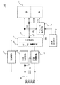
図1は、本発明の実施の形態1における非接触型ICカ−ド100の要部の構成を示した図であり、図7に示した従来の非接触型ICカード900と共通する構成要素には、同一に参照番号及び参照符号を付し、その説明を省略する。なお、本発明が適用される非接触型ICカードのデータの送受信方式は、信号重畳方式であっても、信号分離方式であっても構わない。
【0024】
図1に示す非接触型ICカ−ド100が、従来の非接触型ICカ−ド900と異なる点は、メモリ1のデータ保護領域B2にデータを書込む場合に、その指定された書き込みアドレスを制御する状態設定回路3と、アドレス非選択回路4とを備えることにある。
【0025】
図1を参照して、本発明の実施の形態1における非接触型ICカード100の構成について説明する。
【0026】
アドレス非選択回路4は、入力として主制御回路2から出力されるライトイネーブル信号REと、アドレス線L1からアドレス信号ADとを受ける。ここで、アドレス信号ADとは、データ線L2上のデータDTが書込まれるデータ保護領域B2の位置を指定する信号であり、ライトイネーブル信号REとは、データ保護領域B2へのデータ書き込み動作を指定する信号である。アドレス非選択回路4は、後述する状態設定回路3の制御をうけて、アドレス信号ADに応じて、アドレス選択信号ACを出力する。
【0027】
状態設定回路3は、上記に説明したアドレス非選択回路4を制御する回路である。
【0028】
アドレス非選択回路4から出力されるアドレス選択信号ACは、この状態設定回路3の状態(活性状態/非活性状態)に基づき変化する。より具体的には、状態設定回路3が活性状態である場合には、アドレスADによって指定される位置をデータを書込む位置として選択するアドレス選択信号ACが出力され、非活性状態である場合には、アドレス信号ADによって指定される位置への書込みを禁止する(非選択状態)アドレス選択信号ACが出力される。
【0029】
データDTは、このアドレス非選択回路4から出力されるアドレス選択信号ACに基づき、データ保護領域B2の該当する位置に書込まれる。
【0030】
続いて、本発明の実施の形態1における非接触型ICカード100の動作について説明する。
【0031】
先ず、状態設定回路3が活性状態にある場合には、ライトイネーブル信号REと、アドレス信号ADとを受けたアドレス非選択回路4から、アドレス信号ADによって指定される位置を選択するアドレス選択信号ACが出力される。この場合は、データ保護領域B2の該当する位置に、データDTが書込まれる。
【0032】
一方、状態設定回路3が非活性化状態にある場合には、ライトイネーブル信号REと、アドレス信号ADとを受けたアドレス非選択回路4から、アドレス信号ADによって指定される位置を非選択状態にするアドレス選択信号ACが出力される。この場合は、データDTは、データ保護領域B2に書込まれない。
【0033】
このような状態設定回路3としては、ヒューズを使用するものが挙げられる。例えば、ヒューズを使用する場合は、ヒューズ切断前には、データを何度でもデータ保護領域B2に書込むことができるが、ヒューズを切断すると、データ保護領域B2のデータの書き換えができなくなる。なお、ヒューズを切断する方法としては、高電圧印加、レーザカット、そして誘導加熱等の方法が挙げられる。
【0034】
すなわち、非接触型ICカード100は、状態設定回路3の状態を制御することによって、データ保護領域B2に秘密保守が必要とされるデータを記憶した(簡単のため、この状態を保護データ記憶状態と呼ぶ)後に、データの書き換えを目的とするデータ保護領域B2へのアクセスを不可能とすることができる。
【0035】
以上のように、非接触型ICカード100は、データの書込動作が行なわれる場合に、データ保護領域のアドレス選択を制御することができるため、データ保護領域に予め記憶してあるデータの改ざんを防止することが可能となる。
【0036】
[実施の形態2]
本発明の実施の形態2は、本発明の実施の形態1と同じく、非接触型ICカードにおいて、メモリのデータ保護領域にデータの書込みが行なわれる場合に、その書き込みアドレスを制御することによって、データ保護領域に記憶されたデータの書き換え防止を可能とするものである。
【0037】
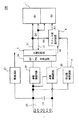
図2は、本発明の実施の形態2における非接触型ICカ−ド200の要部の構成を示した図であり、図1に示した非接触型ICカード100と共通する構成要素には、同一に参照番号及び参照符号を付し、その説明を省略する。
【0038】
図2に示す非接触型ICカ−ド100が、従来の非接触型ICカ−ド900と異なる点は、メモリのデータ保護領域にデータを書込む場合に、その指定された書き込みアドレスを制御するコマンド検知回路5と、アドレス非選択回路6とを備え、主制御回路12から出力されるコマンドによって、これらの回路の制御をおこなうことにある。
【0039】
図2を参照して、本発明の実施の形態2における非接触型ICカード200の構成について説明する。
【0040】
アドレス非選択回路6は、入力としてアドレス線L1からアドレス信号ADを受ける。ここで、アドレス信号ADとは、データ線L2上のデータDTが書込まれるデータ保護領域B2の位置を指定する信号である。アドレス非選択回路6は、後述するコマンド検知回路5の制御を受けて、アドレス信号ADに応じて、アドレス選択信号ACを出力する。
【0041】
コマンド検知回路5は、主制御回路12から出力されるアドレス制御コマンドCOMを受けて、アドレス非選択回路6を制御する。ここで、アドレス制御コマンドCOMとは、アドレス信号ADに基づくデータ保護領域B2へのデータ書き込み動作を許可もしくは禁止するコマンドである。
【0042】
アドレス非選択回路6から出力されるアドレス選択信号ACは、このコマンド検知回路5の状態に従って変化する。より具体的には、コマンド検知回路5によって、データ保護領域B2が書込み許可状態であると検知された場合には、アドレスADによって指定される位置をデータを書込む位置として選択するアドレス選択信号ACが出力される。一方、データ保護領域B2が書込み禁止状態であると検知された場合には、アドレス信号ADによって指定される位置を非選択状態とするアドレス選択信号ACが出力される。
【0043】
データDTは、このアドレス非選択回路6から出力されるアドレス選択信号ACに基づき、データ保護領域B2の該当する位置に書込まれる。
【0044】
続いて、本発明の実施の形態2における非接触型ICカード200の動作について説明する。
【0045】
主制御回路12からデータの書き込みを許可するアドレス制御コマンドCOMが出力された場合、コマンド検知回路5によってこれが検知されると、アドレス非選択回路6から、アドレス信号ADによって指定される位置を選択するアドレス選択信号ACが出力される。この場合は、データ保護領域B2の該当する位置に、データDTが書込まれる。
【0046】
一方、主制御回路12からデータの書き込みを禁止するアドレス制御コマンドCOMが出力された場合、コマンド検知回路5によってこれが検知されると、アドレス非選択回路6から、アドレス信号ADによって指定される位置を非選択状態にするアドレス選択信号ACが出力される。この場合は、データDTは、データ保護領域B2に書込まれない。
【0047】
すなわち、非接触型ICカード200は、主制御回路12から出力されるコマンドに基づきコマンド検知回路5を制御することによって、データ保護領域B2に秘密保守が必要とされるデータが記憶すること(データ保護領域B2を、保護データ記憶状態にする)、およびデータの書き換えを目的とするデータ保護領域B2へのアクセスを不可能とすることを調整することができる。
【0048】
以上のように、非接触型ICカード200は、データの書込動作が行なわれる場合に、データ保護領域のアドレス選択を制御することができるため、データ保護領域に予め記憶してあるデータの改ざんを防止することが可能となる。
【0049】
[実施の形態3]
本発明の実施の形態3は、非接触型ICカードにおいて、データ通信用の周波数に応じて、データ保護領域へのアクセスを制御することによって、データ保護領域に一度記憶したデータの書き換えを防止することを可能とするものである。
【0050】
図3は、本発明の実施の形態3における非接触型ICカ−ド300の要部の構成を示した図であり、図1に示した非接触型ICカード100と共通する構成要素には、同一に参照番号及び参照符号を付し、その説明を省略する。
【0051】
図3に示す非接触型ICカ−ド300が、従来の非接触型ICカ−ド900と異なる点は、周波数検知回路7と、アドレス非選択回路8とを備えることにある。
【0052】
図3を参照して、本発明の実施の形態3における非接触型ICカード300の構成について説明する。
【0053】
周波数検知回路7は、同調回路20が受けた受信電波の周波数を検知する回路であって、図示しない内部には、バンドパスフィルタとスイッチ回路とを備える。周波数検知回路7は、受信電波のキャリア周波数が特定周波数F1である場合には、目的とする電波を受信したことを検知する。
【0054】
アドレス非選択回路8は、入力としてアドレス線L1からアドレス信号ADを受け、主制御回路2からライトイネーブル信号REを受ける。ここで、アドレス信号ADとは、データ線L2上のデータDTが書込まれるデータ保護領域B2の位置を指定する信号である。
【0055】
アドレス非選択回路8は、周波数検知回路7の制御を受けて、アドレス信号ADに応じて、アドレス選択信号ACを出力する。より具体的には、周波数検知回路7が目的とする電波(特定周波数F1)を受信したと検知した場合には、アドレス信号ADによって指定される位置をデータを書込む位置として選択するアドレス選択信号ACが出力され、それ以外(特定周波数F1以外)の場合には、アドレス信号ADによって指定される位置を非選択状態にするアドレス選択信号ACが出力される。
【0056】
データDTは、このアドレス選択信号ACに基づき、データ保護領域B2の該当する位置に書込まれる。
【0057】
図3を参照して、非接触型ICカード300の動作について具体的に説明する。
【0058】
キャリア周波数がF1である電波を受けると、上記に説明したように、アドレス非選択回路8から、アドレス信号ADによって指定される位置を選択するアドレス選択信号ACが出力される。この場合、データDTは、データ保護領域B2の該当する位置に書込まれる。
【0059】
一方、キャリア周波数がF1と異なる、本来の周波数F0である電波を受けると、アドレス非選択回路8から、アドレス信号ADによって指定される位置を非選択状態にするアドレス選択信号ACが出力される。この場合、データDTは、データ保護領域B2に書込まれない。
【0060】
すなわち、非接触型ICカード300は、異なる周波数を使用することによって、データ保護領域B2に秘密保守が必要とされるデータを記憶すること(データ保護領域B2を、保護データ記憶状態にする)、およびデータの書き換えを目的とするデータ保護領域B2へのアクセスを不可能とすることを調整することができる。
【0061】
以上のように、非接触型ICカード300は、データ通信用の電波の周波数に応じて、データ保護領域へのアクセスを制御することができるため、データ保護領域に予め記憶してあるデータの改ざんを防止することが可能となる。
【0062】
[実施の形態4]
本発明の実施の形態4は、非接触型ICカードにおいて、メモリのデータ保護領域にデータの書込みが行なわれる場合に、その書込みデータを制御することによって、目的とするデータの改ざんを阻止することを可能とするものである。
【0063】
図4は、本発明の実施の形態4における非接触型ICカ−ド400の要部の構成を示した図であり、図1に示した非接触型ICカード100と共通する構成要素には、同一に参照番号及び参照符号を付し、その説明を省略する。
【0064】
図4に示す非接触型ICカ−ド400が、従来の非接触型ICカ−ド900と異なる点は、メモリ1のデータ保護領域B2に書込むデータを制御する入力データ固定回路9を備えることにある。
【0065】
図4を参照して、本発明の実施の形態4における非接触型ICカード400の構成について説明する。
【0066】
入力データ固定回路9は、メモリ1のデータ保護領域B2の各位置の状態を固定する回路である。
【0067】
入力データ固定回路9は、入力としてデータ線L2からデータDT1を受け、これを変換して、データDT2を出力する。データDT2は、データ保護領域B2の書込みデータとなる。
【0068】
この入力データ固定回路9から出力されるデータDT2の値は、データ保護領域B2の初期状態に基づき決定されるものとする。例えば、データ保護領域B2の全てのビットの状態を”1”とすれば、データDT2は、常にその逆の極性にある”0”の値を出力する。すなわち、”1”の値に相当するデータDT1が主制御回路2から出力された場合、データ保護領域B2へのデータの書込は行なわれない。
【0069】
図4を参照して、非接触型ICカード400の動作について具体的に説明する。
【0070】
メモリ1のデータ保護領域B2の各ビットの初期状態をすべて”1”(ビットの状態を”1111”)に設定したとする。この場合、データDT1を受ける入力データ固定回路9からは、各ビットに対して、”0”のデータDT2のみが出力される。
【0071】
先ず、秘密保守が必要とされるデータをデータ保護領域B2に書込(保護データ記憶状態)む。この保護データ記憶状態を仮に、”1100”とする。上記で説明したように、入力データ固定回路9から出力されるデータDT2は”0”である。従って、一度”0”の状態になったビットを、”1”の状態に戻すことはできない。この結果、これ以降、データ保護領域B2の状態(”1100”)を、例えば、”1101”に書き換えることはできない。
【0072】
すなわち、非接触型ICカード400のデータ保護領域B2は、OTP(一回だけ書き換え可能な不揮発性メモリ)ROMとして機能することになり、データ保護領域に一度データを記憶した後は、そのデータの書き換えを行なおうとしても、目的とするデータに設定することができない確率が極めて高くなる。
【0073】
以上のように、非接触型ICカード400は、データの書込動作が行なわれる場合に、データ保護領域への書き込みデータを制御することができるため、データ保護領域に一度記憶したデータを書き換えて使用することを阻止することができる。
【0074】
[実施の形態5]
本発明の実施の形態5は、非接触型ICカードにおいて、メモリのデータ保護領域にデータの書込みが行なわれる場合に、その書込みアドレスを制御することによって、目的とするデータの改ざんを阻止することを可能とするものである。
【0075】
図5は、本発明の実施の形態5における非接触型ICカ−ド500の要部の構成を示した図であり、図1に示した非接触型ICカード100と共通する構成要素には、同一に参照番号及び参照符号を付し、その説明を省略する。
【0076】
図5に示す非接触型ICカ−ド500が、従来の非接触型ICカ−ド900と異なる点は、メモリ1のデータ保護領域B2に書込む場合に、その指定された書込アドレスを制御する状態設定回路10と、アドレス非選択回路11とを備えることにある。
【0077】
図5を参照して、本発明の実施の形態5における非接触型ICカード500の構成について説明する。
【0078】
アドレス非選択回路11は、入力として主制御回路2から出力されるライトイネーブル信号REと、アドレス線L1からアドレス信号ADを受ける。ここで、アドレス信号ADとは、データ線L2上のデータDTが書込まれるデータ保護領域B2の位置を指定する信号である。アドレス非選択回路11は、後述する状態設定回路10の制御を受けて、アドレス信号ADに応じて、アドレス選択信号ACを出力する。
【0079】
状態設定回路10は、上記に説明したアドレス非選択回路11を制御する回路である。
【0080】
アドレス非選択回路11から出力されるアドレス選択信号ACは、この状態設定回路10の状態(活性状態/非活性状態)に従って変化する。より具体的には、状態設定回路10が活性状態である場合には、アドレス信号ADによって指定される位置をデータの書込み位置として選択するアドレス選択信号ACが出力され、非活性状態である場合には、アドレス信号ADによって指定される位置以外の位置を選択(もしくは、いずれも選択しない)するアドレス選択信号ACが出力される。
【0081】
データDTは、このアドレス非選択回路11から出力されるアドレス選択信号ACに基づき、データ保護領域B2の該当する位置に書込まれる。
【0082】
続いて、本発明の実施の形態5における非接触型ICカード500の動作について説明する。
【0083】
先ず、状態設定回路10が活性状態にある場合には、ライトイネーブル信号REと、アドレス信号ADとを受けたアドレス非選択回路11から、アドレス信号ADによって指定される位置を選択するアドレス選択信号ACが出力される。この場合は、データ保護領域B2の該当する位置に、データDTが書込まれる。
【0084】
一方、状態設定回路10が非活性化状態にある場合には、ライトイネーブル信号REと、アドレス信号ADとを受けたアドレス非選択回路11から、アドレス信号ADによって指定される位置と異なる位置を選択する(もしくは、いずれも選択しない)アドレス選択信号ACが出力される。この場合は、データDTは、データ保護領域B2の目的とする位置に書込まれない。
【0085】
このような状態設定回路10としては、前述したようにヒューズが挙げられる。
【0086】
すなわち、非接触型ICカード500は、状態設定回路10の状態を制御することによって、データ保護領域B2に秘密保持が必要とされるデータを記憶した(保護データ記憶状態)後には、書き換え行為が発生しても、目的とするデータの書き換えを不可能とすることができる。
【0087】
以上のように、非接触型ICカード500は、データの書込動作が行なわれる場合に、データ保護領域のアドレス選択を制御することができるため、データ保護領域に予め記憶してあるデータを書き換えて使用することを阻止することが可能となる。
【0088】
[実施の形態6]
本発明の実施の形態6は、非接触型ICカードにおいて、データ保護領域に該当する記憶媒体としてOTP(一回だけ書き換え可能な不揮発性メモリ)ROMを備えるものである。
【0089】
図6は、本発明の実施の形態6における非接触型ICカ−ド600の要部の構成を示した図であり、図1に示した非接触型ICカ−ド100の構成と共通する構成要素については、同一の参照符号を付し、その説明は省略する。
【0090】
図6に示す非接触型ICカ−ド600が、従来の非接触型ICカ−ド900と異なる点は、メモリ1の代わって、メモリ15と、メモリ16とを備えることにある。
【0091】
図6を参照して、本発明の実施の形態6における非接触型ICカード600の構成について説明する。
【0092】
メモリ15は、書き換え可能なデータを記憶する記憶媒体であり、メモリ16は、秘密保持が必要とされるデータを記憶する記憶媒体である。
【0093】
具体的には、メモリ15は、EEPROMやフラッシュメモリなどの随時書き換え可能な不揮発性のメモリで構成し、メモリ16は、EPROMに代表される1回だけ書き換え可能なメモリで構成する。
【0094】
続いて、本発明の実施の形態6における非接触型ICカード600の動作について説明する。なお、簡単のため、メモリ16としてEPROMを使用したものとして説明する。
【0095】
主制御回路2から出力される保持すべきデータは、メモリ15、もしくはメモリ16に記憶される。
【0096】
この場合、メモリ16は、EPROMであり、一度図示しないメモリセルに電荷がチャージされた後は、紫外線をあてなければその電荷をディスチャージすることはできない。従って、仮にメモリセルに電荷をチャージした状態を1の状態とし、ディスチャージした状態を0の状態とみなすと、ICカード600を封止した後は、メモリ16に対して、0の状態にあるメモリセルを1の状態にすることはできるが、1の状態にあるメモリセルを0の状態に書き換えることはできない。
【0097】
従って、メモリ16に一度記憶されたデータの書き換えを行なおうとしても、目的とするデータに書き換えられる可能性は極めて低い。
【0098】
以上のように、非接触型ICカード600は、保護すべきデータを記憶する媒体としてOTPROMを使用することにより、データの改ざん効率を極めて低く抑えることがができる。
【0099】
【発明の効果】
以上のように、本発明によれば、データの書き換えを制御することにより、秘密保守が必要とされるデータが記憶されている記憶領域の書き換えを防止することができる。
【0100】
また、本発明によれば、秘密保守が必要とされるデータが記憶されている記憶領域の書き換えを制御することができるので、非接触型ICカードの信頼性を飛躍的に向上することができる。
【図面の簡単な説明】
【図1】本発明の実施の形態1における非接触型ICカード100の要部の構成を示した図である。
【図2】本発明の実施の形態2における非接触型ICカード200の要部の構成を示した図である。
【図3】本発明の実施の形態3における非接触型ICカード300の要部の構成を示した図である。
【図4】本発明の実施の形態4における非接触型ICカード400の要部の構成を示した図である。
【図5】本発明の実施の形態5における非接触型ICカード500の要部の構成を示した図である。
【図6】本発明の実施の形態6における非接触型ICカード600の要部の構成を示した図である。
【図7】従来の非接触型ICカード900の構成を概略的に表した図である。
【符号の説明】
1、15、16 メモリ
2、12 主制御回路
3、10 状態設定回路
4、6、8、11 アドレス非選択回路
5 コマンド検知回路
7 周波数検知回路
9 入力データ固定回路
20 同調回路
C0 コンデンサ
L コイル
100〜600、900 非接触型ICカード[0001]
BACKGROUND OF THE INVENTION
The present invention relates to a non-contact type IC card, and more particularly to a non-contact type IC card that can protect data stored therein and prevent falsification of data.
[0002]
[Prior art]
Conventionally, there is a non-contact type IC card that performs data communication with an interrogator installed outside. For example, ski lift tickets, transportation commuter passes, prepaid cards, and the like are typical examples.
[0003]
FIG. 7 is a block diagram schematically showing a basic configuration of a conventional non-contact
[0004]
The conventional non-contact
[0005]
The
[0006]
The amplification /
[0007]
Referring to FIG. 7, a conventional non-contact
[0008]
The
[0009]
The memory 1 includes a normal data storage area B1 and a data protection area B2. The memory 1 receives the data DA through the data line L2, and receives an address signal AD (write position) for writing the data DA through the address line L1. Here, in the data protection area B2, data for which secret maintenance is required to guarantee normal data communication and rewriting is prohibited is stored. An example of such data is an ID number in an ID card that holds personal information.
[0010]
Further, the
[0011]
[Problems to be solved by the invention]
However, in the conventional non-contact
[0012]
Therefore, the present invention has been made to solve such a problem, and its purpose is a non-contact type IC that can prevent rewriting of a storage area in which data requiring secret maintenance is stored. To provide a card.
[0013]
Another object of the present invention is to provide a highly reliable non-contact type IC card by controlling rewriting of a storage area in which data requiring secret maintenance is stored.
[0018]
[Means for Solving the Problems]
In order to solve the above problems, a non-contact type IC card according to an aspect of the present invention is A non-contact type IC card that performs data communication in response to data received from outside, the first storage unit storing data that requires secret maintenance, and data other than the data stored in the first storage unit Second storage means for storing the data, control means for performing control for writing the data at the position of the corresponding first storage means or second storage means in accordance with the contents of the data, and control Selection means for selecting whether or not to write data to the position of the first storage means designated by the means, and state setting means for controlling selection of the selection means, and the state setting means is in the first state In this case, the data is written as it is in the position of the first storage means designated by the control means, and when the state setting means is in a second state different from the first state, the data is designated by the control means. Other than the position of the first storage means It is written to the location.
[0019]
Preferably, The state setting means is composed of a fuse. When the state setting means is in the first state, the fuse is in an electrically conductive state, and in the second state, the fuse is in an electrically nonconductive state.
[0022]
DETAILED DESCRIPTION OF THE INVENTION
[Embodiment 1]
In the first embodiment of the present invention, when data is written to the data protection area of the memory in the non-contact type IC card, the data stored in the data protection area is controlled by controlling the write address. It is possible to prevent rewriting.
[0023]
FIG. 1 is a diagram showing a configuration of a main part of a non-contact
[0024]
The non-contact
[0025]
With reference to FIG. 1, the structure of non-contact
[0026]
The address non-selection circuit 4 receives the write enable signal RE output from the
[0027]
The state setting circuit 3 is a circuit that controls the address non-selection circuit 4 described above.
[0028]
The address selection signal AC output from the address non-selection circuit 4 changes based on the state (active state / inactive state) of the state setting circuit 3. More specifically, when the state setting circuit 3 is in an active state, an address selection signal AC for selecting a position specified by the address AD as a position to write data is output, and when the state setting circuit 3 is in an inactive state. Outputs an address selection signal AC that inhibits writing to the position specified by the address signal AD (non-selected state).
[0029]
Data DT is written at a corresponding position in data protection region B2 based on address selection signal AC output from address non-selection circuit 4.
[0030]
Subsequently, the operation of the non-contact
[0031]
First, when the state setting circuit 3 is in an active state, an address selection signal AC for selecting a position specified by the address signal AD from the address non-selection circuit 4 receiving the write enable signal RE and the address signal AD. Is output. In this case, data DT is written at the corresponding position in data protection area B2.
[0032]
On the other hand, when the state setting circuit 3 is in the inactive state, the position specified by the address signal AD is set to the non-selected state from the address non-selecting circuit 4 that receives the write enable signal RE and the address signal AD. The address selection signal AC to be output is output. In this case, data DT is not written to data protection area B2.
[0033]
An example of such a state setting circuit 3 is one that uses a fuse. For example, when a fuse is used, data can be written into the data protection area B2 any number of times before the fuse is cut. However, when the fuse is cut, data in the data protection area B2 cannot be rewritten. Examples of the method for cutting the fuse include high voltage application, laser cutting, induction heating, and the like.
[0034]
That is, the non-contact
[0035]
As described above, the
[0036]
[Embodiment 2]
In the second embodiment of the present invention, as in the first embodiment of the present invention, in the non-contact type IC card, when data is written to the data protection area of the memory, by controlling the write address, The data stored in the data protection area can be prevented from being rewritten.
[0037]
FIG. 2 is a diagram showing a configuration of a main part of the non-contact
[0038]
The non-contact
[0039]
With reference to FIG. 2, the structure of non-contact
[0040]
The
[0041]
The
[0042]
The address selection signal AC output from the
[0043]
The data DT is written at a corresponding position in the data protection area B2 based on the address selection signal AC output from the
[0044]
Subsequently, the operation of the non-contact
[0045]
When the address control command COM permitting data writing is output from the
[0046]
On the other hand, when the address control command COM prohibiting data writing is output from the
[0047]
In other words, the non-contact
[0048]
As described above, the non-contact
[0049]
[Embodiment 3]
The third embodiment of the present invention prevents rewriting of data once stored in the data protection area by controlling access to the data protection area in accordance with the frequency for data communication in the non-contact type IC card. It is possible to do that.
[0050]
FIG. 3 is a diagram showing a configuration of a main part of the non-contact
[0051]
The non-contact
[0052]
With reference to FIG. 3, the structure of non-contact
[0053]
The frequency detection circuit 7 is a circuit that detects the frequency of the received radio wave received by the
[0054]
The
[0055]
The
[0056]
Data DT is written at a corresponding position in data protection area B2 based on address selection signal AC.
[0057]
The operation of the non-contact
[0058]
When receiving a radio wave having a carrier frequency of F1, as described above, the
[0059]
On the other hand, when receiving a radio wave having a carrier frequency different from F1 and having the original frequency F0, the
[0060]
That is, the non-contact
[0061]
As described above, the non-contact
[0062]
[Embodiment 4]
In Embodiment 4 of the present invention, when data is written to a data protection area of a memory in a non-contact type IC card, the write data is controlled to prevent alteration of the target data. Is possible.
[0063]
FIG. 4 is a diagram showing a configuration of a main part of the non-contact
[0064]
The non-contact
[0065]
With reference to FIG. 4, the structure of non-contact
[0066]
The input data fixing circuit 9 is a circuit that fixes the state of each position in the data protection area B2 of the memory 1.
[0067]
The input data fixing circuit 9 receives data DT1 from the data line L2 as input, converts it, and outputs data DT2. The data DT2 becomes write data in the data protection area B2.
[0068]
It is assumed that the value of the data DT2 output from the input data fixing circuit 9 is determined based on the initial state of the data protection area B2. For example, if the state of all the bits in the data protection area B2 is “1”, the data DT2 always outputs a value of “0” having the opposite polarity. That is, when data DT1 corresponding to the value “1” is output from
[0069]
The operation of the non-contact
[0070]
Assume that the initial state of each bit in the data protection area B2 of the memory 1 is set to “1” (the bit state is “1111”). In this case, only “0” data DT2 is output for each bit from the input data fixing circuit 9 that receives the data DT1.
[0071]
First, data requiring secret maintenance is written into the data protection area B2 (protected data storage state). This protected data storage state is assumed to be “1100”. As described above, the data DT2 output from the input data fixing circuit 9 is “0”. Therefore, a bit once in a “0” state cannot be returned to a “1” state. As a result, thereafter, the state (“1100”) of the data protection area B2 cannot be rewritten to “1101”, for example.
[0072]
That is, the data protection area B2 of the non-contact
[0073]
As described above, the non-contact
[0074]
[Embodiment 5]
In
[0075]
FIG. 5 is a diagram showing a configuration of a main part of the non-contact
[0076]
The non-contact
[0077]
With reference to FIG. 5, the structure of non-contact
[0078]
The
[0079]
The
[0080]
The address selection signal AC output from the
[0081]
The data DT is written at a corresponding position in the data protection area B2 based on the address selection signal AC output from the
[0082]
Subsequently, the operation of the non-contact
[0083]
First, when the
[0084]
On the other hand, when the
[0085]
Such a
[0086]
That is, the non-contact
[0087]
As described above, the non-contact
[0088]
[Embodiment 6]
In
[0089]
FIG. 6 is a diagram showing a configuration of a main part of the non-contact
[0090]
The non-contact
[0091]
With reference to FIG. 6, the structure of non-contact
[0092]
The
[0093]
Specifically, the
[0094]
Subsequently, the operation of the non-contact
[0095]
Data to be held output from the
[0096]
In this case, the
[0097]
Therefore, even if the data once stored in the
[0098]
As described above, the non-contact
[0099]
【The invention's effect】
As described above, according to the present invention, it is possible to prevent rewriting of a storage area in which data requiring secret maintenance is stored by controlling rewriting of data.
[0100]
Further, according to the present invention, since rewriting of a storage area in which data requiring secret maintenance is stored can be controlled, the reliability of the non-contact type IC card can be greatly improved. .
[Brief description of the drawings]
FIG. 1 is a diagram illustrating a configuration of a main part of a non-contact
FIG. 2 is a diagram showing a configuration of a main part of a non-contact
FIG. 3 is a diagram showing a configuration of a main part of a non-contact
FIG. 4 is a diagram showing a configuration of a main part of a non-contact
FIG. 5 is a diagram showing a configuration of a main part of a non-contact
FIG. 6 is a diagram showing a configuration of a main part of a non-contact
7 is a diagram schematically showing a configuration of a conventional non-contact
[Explanation of symbols]
1, 15, 16 memory
2,12 Main control circuit
3, 10 State setting circuit
4, 6, 8, 11 Address non-selection circuit
5 Command detection circuit
7 Frequency detection circuit
9 Input data fixing circuit
20 Tuning circuit
C0 capacitor
L coil
100 to 600, 900 Non-contact type IC card
Claims (2)
秘密保守が必要とされる前記データを記憶する第1の記憶手段と、
前記第1の記憶手段に記憶する前記データ以外のデータを記憶する第2の記憶手段と、
前記データの内容に応じて、該当する前記第1の記憶手段もしくは前記第2の記憶手段の位置に、前記データを書込むための制御を行なう制御手段と、
前記制御手段が指定した前記第1の記憶手段の前記位置に前記データを書込むか否かを選択する選択手段と、
前記選択手段の選択を制御する状態設定手段とを備え、
前記状態設定手段が第1の状態にある場合には、前記データは前記制御手段が指定した前記第1の記憶手段の前記位置にそのまま書込まれ、前記状態設定手段が第1の状態と異なる第2の状態にある場合には、前記データは前記制御手段が指定した前記第1の記憶手段の前記位置以外の位置に書込まれる、非接触型ICカード。A non-contact type IC card that performs data communication in response to data received from the outside,
First storage means for storing said data for which secret maintenance is required;
Second storage means for storing data other than the data stored in the first storage means;
Control means for performing control for writing the data in the corresponding position of the first storage means or the second storage means according to the content of the data;
Selecting means for selecting whether or not to write the data at the position of the first storage means designated by the control means;
State setting means for controlling selection of the selection means,
When the state setting means is in the first state, the data is written as it is in the position of the first storage means designated by the control means, and the state setting means is different from the first state. In the second state, the data is written in a position other than the position of the first storage means designated by the control means.
Priority Applications (8)
| Application Number | Priority Date | Filing Date | Title |
|---|---|---|---|
| JP00886997A JP3689213B2 (en) | 1997-01-21 | 1997-01-21 | Non-contact IC card |
| CA002277905A CA2277905C (en) | 1997-01-21 | 1998-01-09 | Non-contact type ic card |
| PCT/JP1998/000060 WO1998032097A1 (en) | 1997-01-21 | 1998-01-09 | Non-contact ic card |
| AU53427/98A AU5342798A (en) | 1997-01-21 | 1998-01-09 | Non-contact ic card |
| US09/341,676 US20020162893A1 (en) | 1997-01-21 | 1998-01-09 | Non-contact ic card |
| EP98900202A EP0955602B1 (en) | 1997-01-21 | 1998-01-09 | Non-contact ic card |
| DE69801150T DE69801150T2 (en) | 1997-01-21 | 1998-01-09 | CONTACTLESS CHIP CARD |
| US10/287,494 US6679424B2 (en) | 1997-01-21 | 2002-11-05 | Non contact type IC card |
Applications Claiming Priority (1)
| Application Number | Priority Date | Filing Date | Title |
|---|---|---|---|
| JP00886997A JP3689213B2 (en) | 1997-01-21 | 1997-01-21 | Non-contact IC card |
Related Child Applications (1)
| Application Number | Title | Priority Date | Filing Date |
|---|---|---|---|
| JP2005111178A Division JP2005267656A (en) | 2005-04-07 | 2005-04-07 | Noncontact type ic card |
Publications (2)
| Publication Number | Publication Date |
|---|---|
| JPH10207995A JPH10207995A (en) | 1998-08-07 |
| JP3689213B2 true JP3689213B2 (en) | 2005-08-31 |
Family
ID=11704704
Family Applications (1)
| Application Number | Title | Priority Date | Filing Date |
|---|---|---|---|
| JP00886997A Expired - Fee Related JP3689213B2 (en) | 1997-01-21 | 1997-01-21 | Non-contact IC card |
Country Status (7)
| Country | Link |
|---|---|
| US (2) | US20020162893A1 (en) |
| EP (1) | EP0955602B1 (en) |
| JP (1) | JP3689213B2 (en) |
| AU (1) | AU5342798A (en) |
| CA (1) | CA2277905C (en) |
| DE (1) | DE69801150T2 (en) |
| WO (1) | WO1998032097A1 (en) |
Families Citing this family (16)
| Publication number | Priority date | Publication date | Assignee | Title |
|---|---|---|---|---|
| EP1117064B1 (en) | 1998-07-31 | 2005-01-26 | Matsushita Electric Industrial Co., Ltd. | A dual-purpose non-contact chip card, a system with terminal appartus and card, and a communication method |
| JP2003528404A (en) * | 2000-03-21 | 2003-09-24 | コーニンクレッカ フィリップス エレクトロニクス エヌ ヴィ | Communication device for fast and simultaneous writing on multiple data carriers and data carrier for such a communication device |
| WO2002011019A1 (en) | 2000-08-01 | 2002-02-07 | First Usa Bank, N.A. | System and method for transponder-enabled account transactions |
| WO2005009063A1 (en) * | 2003-07-18 | 2005-01-27 | Koninklijke Philips Electronics N.V. | Circuit for a data carrier, which circuit can be switched from an energy-saving processing mode to a normal-consumption processing mode |
| JP2005109652A (en) * | 2003-09-29 | 2005-04-21 | Casio Comput Co Ltd | Portable apparatus having electronic tag, server and program |
| JP4380323B2 (en) * | 2003-12-25 | 2009-12-09 | ブラザー工業株式会社 | Wireless tag reader / writer, tag tape, and wireless tag creation method |
| US8918900B2 (en) * | 2004-04-26 | 2014-12-23 | Ivi Holdings Ltd. | Smart card for passport, electronic passport, and method, system, and apparatus for authenticating person holding smart card or electronic passport |
| JP2006085548A (en) * | 2004-09-17 | 2006-03-30 | Internatl Business Mach Corp <Ibm> | Radio ic chip and its ic module |
| KR100881025B1 (en) * | 2006-11-07 | 2009-02-05 | 삼성전자주식회사 | Apparatus and method for managing data security |
| JP5080833B2 (en) * | 2007-03-16 | 2012-11-21 | 株式会社バッファロー | Memory device and manufacturing method thereof |
| FR2921175A1 (en) | 2007-09-14 | 2009-03-20 | Sagem Securite Sa | Chip card i.e. contact chip card, for use as e.g. bank card, has antenna for exchanging data with external device, RAM including storage zone dedicated for exchanged data, and processing unit for securing zone and storing data in zone |
| JP4729771B2 (en) * | 2008-07-17 | 2011-07-20 | Necディスプレイソリューションズ株式会社 | Electronic device and unauthorized rewrite suppression method |
| JP4548524B2 (en) | 2008-07-29 | 2010-09-22 | ソニー株式会社 | COMMUNICATION DEVICE, PROGRAM, COMMUNICATION METHOD, AND COMMUNICATION SYSTEM |
| JP2012212244A (en) * | 2011-03-30 | 2012-11-01 | Nec Personal Computers Ltd | Storage device |
| KR101080511B1 (en) * | 2011-08-03 | 2011-11-04 | (주) 아이씨티케이 | Integrated circuit chip prevneting leak of identification key and method for certification of the integrated circuit chip |
| US9184915B2 (en) * | 2012-08-30 | 2015-11-10 | Vasco Data Security, Inc. | Strong authentication token with acoustic data input over multiple carrier frequencies |
Family Cites Families (21)
| Publication number | Priority date | Publication date | Assignee | Title |
|---|---|---|---|---|
| JPS61264485A (en) | 1985-05-18 | 1986-11-22 | Hitachi Maxell Ltd | Reader and writer for integrated circuit card |
| FR2591008B1 (en) | 1985-11-30 | 1991-05-17 | Toshiba Kk | PORTABLE ELECTRONIC DEVICE |
| JP2880709B2 (en) * | 1986-09-26 | 1999-04-12 | 株式会社東芝 | Memory control method for IC card |
| JP2514954B2 (en) | 1987-03-13 | 1996-07-10 | 三菱電機株式会社 | IC card |
| JPS63229542A (en) * | 1987-03-19 | 1988-09-26 | Fujitsu Ltd | Electronic card |
| JPH01233690A (en) * | 1988-03-15 | 1989-09-19 | Matsushita Electric Ind Co Ltd | Ic card |
| JPH0652544B2 (en) * | 1988-05-20 | 1994-07-06 | 日本モトローラ株式会社 | CMOS circuit for fuse cutting |
| JPH03240127A (en) | 1990-02-17 | 1991-10-25 | Hitachi Maxell Ltd | Program control system |
| JPH03253397A (en) * | 1990-03-05 | 1991-11-12 | Dainippon Printing Co Ltd | Ic card |
| FR2666671B1 (en) | 1990-09-12 | 1994-08-05 | Gemplus Card Int | METHOD FOR MANAGING AN APPLICATION PROGRAM LOADED IN A MICROCIRCUIT MEDIUM. |
| JPH0770227B2 (en) | 1990-10-01 | 1995-07-31 | 日鉄セミコンダクター株式会社 | Semiconductor memory read operation control method |
| FR2667417B1 (en) | 1990-10-02 | 1992-11-27 | Gemplus Card Int | MICROPROCESSOR CARD DESIGNED TO RECEIVE MULTIPLE PROGRAMS IN PROGRAMMABLE MEMORY. |
| JPH04151893A (en) | 1990-10-09 | 1992-05-25 | Canon Inc | Falling-off preventing method of electronic components |
| JP2543440B2 (en) * | 1990-12-17 | 1996-10-16 | 三菱電機株式会社 | IC card and IC card system |
| JPH04263386A (en) | 1991-02-18 | 1992-09-18 | Fuji Photo Film Co Ltd | Ic memory card |
| DE4205567A1 (en) * | 1992-02-22 | 1993-08-26 | Philips Patentverwaltung | METHOD FOR CONTROLLING ACCESS TO A STORAGE AND ARRANGEMENT FOR IMPLEMENTING THE METHOD |
| JPH0778231A (en) | 1993-09-07 | 1995-03-20 | Toshiba Corp | Memory card |
| US5530232A (en) * | 1993-12-22 | 1996-06-25 | Datamark Services, Inc. | Multi-application data card |
| FR2716280B1 (en) | 1994-02-11 | 1996-04-12 | Solaic Sa | Method for protecting memory card components against fraudulent use. |
| US5521362A (en) | 1994-06-08 | 1996-05-28 | Mci Communications Corporation | Electronic purse card having multiple storage memories to prevent fraudulent usage and method therefor |
| JPH08101902A (en) * | 1994-09-30 | 1996-04-16 | Toppan Printing Co Ltd | Information card |
-
1997
- 1997-01-21 JP JP00886997A patent/JP3689213B2/en not_active Expired - Fee Related
-
1998
- 1998-01-09 WO PCT/JP1998/000060 patent/WO1998032097A1/en active IP Right Grant
- 1998-01-09 DE DE69801150T patent/DE69801150T2/en not_active Expired - Fee Related
- 1998-01-09 US US09/341,676 patent/US20020162893A1/en not_active Abandoned
- 1998-01-09 AU AU53427/98A patent/AU5342798A/en not_active Abandoned
- 1998-01-09 EP EP98900202A patent/EP0955602B1/en not_active Expired - Lifetime
- 1998-01-09 CA CA002277905A patent/CA2277905C/en not_active Expired - Fee Related
-
2002
- 2002-11-05 US US10/287,494 patent/US6679424B2/en not_active Expired - Fee Related
Also Published As
| Publication number | Publication date |
|---|---|
| WO1998032097A1 (en) | 1998-07-23 |
| CA2277905A1 (en) | 1998-07-23 |
| DE69801150T2 (en) | 2002-03-14 |
| CA2277905C (en) | 2002-07-09 |
| EP0955602B1 (en) | 2001-07-18 |
| AU5342798A (en) | 1998-08-07 |
| US6679424B2 (en) | 2004-01-20 |
| US20020162893A1 (en) | 2002-11-07 |
| EP0955602A1 (en) | 1999-11-10 |
| US20030066895A1 (en) | 2003-04-10 |
| JPH10207995A (en) | 1998-08-07 |
| EP0955602A4 (en) | 1999-12-15 |
| DE69801150D1 (en) | 2001-08-23 |
Similar Documents
| Publication | Publication Date | Title |
|---|---|---|
| JP3689213B2 (en) | Non-contact IC card | |
| KR100593272B1 (en) | Minimum voltage radio frequency identification | |
| CN100581066C (en) | Radio tag and radio tag communication distance modification method | |
| US5430447A (en) | Protection against manipulation of batteryless read/write transponders | |
| CA2148145C (en) | Passive transponder | |
| US8610538B2 (en) | Memory-tag data authentication | |
| KR20070106458A (en) | Ic module and cellular phone | |
| JP4701618B2 (en) | Information processing apparatus, information processing method, and computer program | |
| US7889055B2 (en) | IC tag, IC tag system, and method of executing command of the IC tag | |
| US20010045468A1 (en) | Ic card | |
| JP2019028667A (en) | Semiconductor storage device provided with wireless communication function, and writing control method | |
| JP2005267656A (en) | Noncontact type ic card | |
| JP4525084B2 (en) | Loss current interruption circuit and portable terminal | |
| JP2007087168A (en) | Composite portable electronic device and composite ic card | |
| JPH10154216A (en) | Non-contact ic card | |
| Howes et al. | A read/write RFID tag for low cost applications | |
| JP4334538B2 (en) | IC card | |
| JP2006107380A (en) | Information processor, information processing method, memory device and computer program | |
| JP3913029B2 (en) | Non-contact information storage medium | |
| JP2000207506A (en) | Non-contact type ic card system | |
| JPH10187550A (en) | Ic card | |
| JP2006163469A (en) | Radio tag and system using radio tag | |
| US7194570B2 (en) | Method and device for selecting the operating mode of an integrated circuit | |
| JPH10228527A (en) | Frequency storing member having portability and its operating method | |
| JPH0773110A (en) | Data storage system |
Legal Events
| Date | Code | Title | Description |
|---|---|---|---|
| A131 | Notification of reasons for refusal |
Free format text: JAPANESE INTERMEDIATE CODE: A131 Effective date: 20050208 |
|
| A521 | Request for written amendment filed |
Free format text: JAPANESE INTERMEDIATE CODE: A523 Effective date: 20050407 |
|
| TRDD | Decision of grant or rejection written | ||
| A01 | Written decision to grant a patent or to grant a registration (utility model) |
Free format text: JAPANESE INTERMEDIATE CODE: A01 Effective date: 20050524 |
|
| A61 | First payment of annual fees (during grant procedure) |
Free format text: JAPANESE INTERMEDIATE CODE: A61 Effective date: 20050610 |
|
| R150 | Certificate of patent or registration of utility model |
Free format text: JAPANESE INTERMEDIATE CODE: R150 |
|
| FPAY | Renewal fee payment (event date is renewal date of database) |
Free format text: PAYMENT UNTIL: 20080617 Year of fee payment: 3 |
|
| FPAY | Renewal fee payment (event date is renewal date of database) |
Free format text: PAYMENT UNTIL: 20110617 Year of fee payment: 6 |
|
| LAPS | Cancellation because of no payment of annual fees |