JP3684128B2 - Arithmetic encoding / decoding method and arithmetic encoding / decoding device - Google Patents
Arithmetic encoding / decoding method and arithmetic encoding / decoding device Download PDFInfo
- Publication number
- JP3684128B2 JP3684128B2 JP2000041693A JP2000041693A JP3684128B2 JP 3684128 B2 JP3684128 B2 JP 3684128B2 JP 2000041693 A JP2000041693 A JP 2000041693A JP 2000041693 A JP2000041693 A JP 2000041693A JP 3684128 B2 JP3684128 B2 JP 3684128B2
- Authority
- JP
- Japan
- Prior art keywords
- value
- decoding
- arithmetic
- bit
- pixel
- Prior art date
- Legal status (The legal status is an assumption and is not a legal conclusion. Google has not performed a legal analysis and makes no representation as to the accuracy of the status listed.)
- Expired - Fee Related
Links
Images


Description
【0001】
【発明の属する技術分野】
本発明は、算術符号(Arithmetic code)を用いて画像データを符号化する算術符号化方法と、該方法で符号化された画像データを復号化する算術復号化装置に関し、特に多値画像の算術符号化方法と算術復号化装置に関する。
【0002】
【従来の技術】
算術符号は、[0,1)の数値直線上の対応区間(2進小数で[0.0・・・0,0.1・・・1])を各シンボルの生起確率に応じて不等長に分割していき、符号化対象シンボル系列を対応する部分区間に割り当て、再帰的に分割を繰り返していくことにより得られた区間内に含まれる点の座標を少なくとも他の区間と区別できる2進小数で表現して、そのまま符号とするものである。
【0003】
算術符号の方法の代表的なものとして、ITUの機関であるJBIG(Joint Bi−1evel Image Experts Group)で標準化されたJBIG(QM−coder)方法、IBM社が提案しているQ−coder等がある。
【0004】
各方法により使用されている用語が異なるため、ここでは標準方法であるJBIG方法に用いられている用語を使用するが、これによりJBIG方法の算術符号に限定されるものではない。
【0005】
算術符号化では、原理的には算術演算部で乗算処理を必要とするが、乗算処理を行うと算術演算部のハードウェア規模が大きくなったり、乗算処理にかかる処理時間が長くなるといった問題があるため、該算術演算を加減演算に置き換え簡略化した方法が主流になっている。
【0006】
算術演算部内部には、符号化シンボル系列に対応する領域幅(オージェント)を保持するAレジスタと、コードを発生する基となる値を保持するコードレジスタ(Cレジスタ)とがあり、符号化予測値に対する符号化対象シンボルのはずれ確率を確率推定値LSZとして入力し、前記シンボルが予測値に一致したかあるいは不一致かという情報に基づいて、確率推定値LSZと前記2つのレジスタの値から算術演算(加減算)を行ない、該2つのレジスタの値を更新する。
【0007】
確率推定値LSZは、符号化対象シンボルの周辺シンボル情報を数値化したコンテキストごとに持つindex(状態)値から所定の対応表を用いて変換することによって得られる。コンテキストごとに持つ状態値は、所定条件に基づいて更新することにより、符号化シンボル系列固有のパターンを学習することができ、符号化効率を上げることができる。
【0008】
JBIG方法では、Aレジスタの値を10000Hに初期化し、算術演算(符号化あるいは復号化)の結果、Aレジスタの値が8000H未満になると、正規化処理と称して、Aレジスタの値が8000H以上になるまで左シフトを行い、その際に現コンテキストの状態値を更新する。
【0009】
また、Aレジスタの値を左シフトする時、それと同時にCレジスタの値も左シフトする。この時、Cレジスタの再上位からシフトアウトされるデータが符号化データとなる。
【0010】
符号化対象のシンボルの値が0または1しかとらない、2値の画素データである場合、上記算術符号化処理を行なう符号化ブロックの構成は、図1に示すものとなる。
【0011】
<符号化ブロック>
同図において、101は符号化対象画素の2値データPIXを入力する端子、102は2値データPIX信号、103は符号化対象画素の周辺画素データからなるコンテキスト情報、105はコンテキスト情報ごとに予測値とindex(状態)値を保持する予測状態メモリ、106は予測状態メモリ105から出力される予測値、107は予測状態メモリ105から出力される状態値、109は出力された状態値107を確率推定値LSZに変換する確率推定部、111は確率推定部109から出力される確率推定値LSZ、113は排他的NORゲート、114は前記2値データPIXと予測値106との一致/不一致を表わす信号、115は算術符号化演算部、117は算術符号化演算部115から出力される符号化データ(コードデータ)、118は前記予測状態メモリ105の更新を要求するための信号、119は現在の予測値106と状態値107から更新後の予測値と状態値を求める予測状態更新部、120は予測状態更新部119から出力される、更新後の予測値・状態値信号および予測状態メモリ105に該信号を書き込む制御信号等である。
【0012】
次に、図1に示す算術符号化処理ブロックの動作説明を行なう。
【0013】
符号化対象画素の2値データPIXは端子101から入力され、排他的NORゲート113に入力する。一方、コンテキスト情報である103の符号化対象画素の周辺画素データCXi(i=1,2,…,n)が予測状態メモリ105に与えられる。
【0014】
予測状態メモリ105は周辺画素データからなるコンテキスト情報103をアドレスとして、符号化対象画素に対する予測値106とindex(状態)値107を出力する。なお、この状態値107はそれまでに符号化処理して学習した内容に基づいて決まる。予測値106は、0または1の2値であり、排他的NORゲート113に入力される。
【0015】
一方、状態値107は確率推定部109に送られ、ここで確率推定値111に変換される。確率推定値111は、2値データPIXが予測値106と一致しない確率を表わす。状態値107から確率推定値111への変換は、ROMテーブルあるいはデコーダを用いて行なわれる。また、状態値107は予測状態更新部119にも入力される。
【0016】
排他的NORゲート113では、2値データPIXと予測値106との一致/不一致の関係を調べ、一致していれば1を、不一致であれば0を算術符号化演算部115へ送る。
【0017】
算術符号化演算部115では、一致/不一致情報114と、確率推定部109から入力される確率推定値111とに基づいて、後述する符号化処理のための算術演算を行ない、符号化データ117を出力する。
【0018】
算術符号化演算部115における算術演算の過程で上述の正規化処理が行なわれると、信号118を出力し、予測状態更新部119に更新要求を行なう。
【0019】
予測状態更新部119は、入力される状態値107、予測値106及び一致/不一致情報114から、更新後の状態値と予測値を求めて、更新データを予測状態メモリ105に送る。更新データを受信した予測状態メモリ105は、更新要求に基づいて保持内容を更新する。なお、予測状態更新部119において入力状態値106から更新後の状態値を求めるには、ROMテーブルあるいはデコーダ等を用いる。
【0020】
次に、図2に算術符号化演算部115の一構成例を示し、その動作について述べる。
【0021】
同図において、201は領域幅(オージェント)を保持するAレジスタ、203はコードを発生する基となる値を保持するコードレジスタ(Cレジスタ)、205はAレジスタ201の出力値から確率推定値111を減算する減算器、207はCレジスタ203の出力値に減算器205の出力を加算する加算器、209はAレジスタ201へ入力するデータを選択するセレクタ、211はCレジスタへ入力するデータを選択するセレクタ、213はCレジスタからシフトアウトされるコード情報を取り込むシフトレジスタ、215は出力レジスタ、217はシフトレジスタ213に取り込んだビット数をカウントするカウンタ、218はシフトクロックを入力する端子、219はマスク回路、220はマスク回路219によりマスクされたシフトクロック、221は、Aレジスタ201の出力値が8000H(16進)以上であることを検出する検出器である。
【0022】
初期化後の状態では、Aレジスタ201の値は10000H、Cレジスタ203の値は0Hであり、カウンタ217の値は0である。
【0023】
入力された一致/不一致情報114と確率推定値111に基づいて所定の算術演算を行うことにより、1画素を符号化するごとにAレジスタ201とCレジスタ203の値を更新する。そして、Aレジスタ201の正規化処理に伴いCレジスタ203の上位からシフトアウトされるデータをNビット単位にまとめて出力したものが符号化データ117となる。
【0024】
まず入力された確率推定値111は減算器205とセレクタ209に入力する。
【0025】
減算器205では、Aレジスタ201の出力値から、確率推定値111を減算し、その結果をセレクタ209と加算器207へ送る。
【0026】
セレクタ209には確率推定値111も与えられており、一致/不一致情報114が1の時は減算結果を、0の時は確率推定値111を選択し出力する。
【0027】
加算器207では、減算器205から送られてきた減算結果をCレジスタ203の出力値に加算し、加算結果をセレクタ211に送る。セレクタ211には、Cレジスタ203の出力値も直接与えられており、前記一致/不一致情報114が1の時はCレジスタ203の出力値を、0の時は加算結果を選択し出力する。
【0028】
セレクタ209、211それぞれの出力は、それぞれ次のサイクルで、Aレジスタ201、Cレジスタ203に取り込まれる。
【0029】
Aレジスタ201の値が8000H未満の時は、検出器221でそれを検出し、次の算術演算を行う前に正規化処理を行う。それに対し、Aレジスタ201の値が8000H以上の時は、次の算術演算を行う。
【0030】
正規化処理の1つの実現方法は、Aレジスタ201とCレジスタ203のそれぞれにシフト機能を有するレジスタを用い、該レジスタにシフト用のクロック220を与え、Aレジスタ201の値が8000Hになるまで、AレジスタとCレジスタを左シフトするものである。
【0031】
シフト用のクロック220は、検出器221の出力に基づいて、端子218から入力されるシフトクロックをマスク回路219にてマスクすることにより得られる。
【0032】
Aレジスタ201の値が8000H未満のあいだ、入力シフトクロックはマスク回路219を通過し、Aレジスタ201、Cレジスタ203並びに、シフトレジスタ213、カウンタ217に送られる。このシフトクロックが入力する毎に、Aレジスタ201、Cレジスタ203、シフトレジスタ213は1ビット左へシフトし、カウンタ217は1つカウントアップする。
【0033】
シフトレジスタ213へ入力するデータは、Cレジスタ203の最上位ビットであるため、シフトクロック220が各ブロックへ送られるたびに、Cレジスタ203の上位ビットデータがシフトレジスタ213に移ることになる。
【0034】
シフトレジスタ213に移されたビット数はシフトクロック220によりカウントアップするカウンタ217でカウントされていることになり、該カウント値が所定の値に達したところで、カウンタ217は出力レジスタ215へデータ取り込みパルス222を送る。
【0035】
出力レジスタ215はパルス222が入力されるタイミングで、シフトレジスタ213から送られる所定ビット数のデータを一括して受け取り、次のデータ取り込みパルス222が入力されるまで、該データを保持する。
【0036】
なお、Aレジスタ201の値が8000H未満であることを検出器221が検出したときに、不図示の回路により予測状態更新部119へ更新を要求する信号118が出力される。
【0037】
以上説明したような算術演算及び正規化処理により、端子101に入力された2値データPIXが符号化され、符号化データ117が算術符号化演算部115より所定ビット単位で出力される。
【0038】
<復号化ブロック>
次に、図1に示す符号化ブロックに対応した復号化ブロックの構成を図3に示し、その動作を説明する。
【0039】
図3に示す復号化ブロックと、図1に示す符号化ブロックとの大きな違いは、以下の2点である。
【0040】
(1)算術符号化演算部115の替わりに、算術復号化演算部301を用いる。(2)符号化データ306を入力して、着目画素データの値を求める。
その他の構成は基本的に同じであるため、上記違いについて簡単に説明する。
【0041】
まず算術復号化演算部301内部の動作説明から行なう。図4に、算術復号化演算部301の構成を示す。
【0042】
同図において、減算器401は図2の算術符号化演算部115における加算器207を、入力バッファレジスタ403は図2の出力レジスタ215を、また、シフトレジスタ405はシフトレジスタ213をそれぞれ置き換えたものである。
【0043】
入力された確率推定値111は、減算器205とセレクタ209に入力される。減算器205ではAレジスタ201の出力値から、入力された確率推定値111を減算し、その減算結果をセレクタ209と減算器401へ送る。
【0044】
図1の算術符号化演算部115では、一致/不一致情報114に基づいてセレクタ209が動作していたが、算術復号化演算部301では、減算器401における減算結果が正か負かによって、セレクタ209の動作が決まる。
【0045】
減算器401では、Cレジスタ203の出力値から減算器205の出力値を減算し、減算結果をセレクタ211に送り、更に減算結果が正か負かを表す信号302を出力する。信号302は、減算結果が正の場合0、負の場合1という値をとる。
【0046】
この信号302を制御信号として、減算結果が正の場合、セレクタ209は確率推定値111を選択し、減算結果が負の場合、減算器205の出力を選択して出力する。
【0047】
セレクタ211もセレクタ209と同じ信号302により制御される。セレクタ211には減算器401の出力すなわち減算結果と、Cレジスタ203の出力値が入力されている。そして、減算結果が正の場合、減算器401の出力を選択し、減算結果が負の場合、Cレジスタ203の出力を選択して出力する。
【0048】
セレクタ209、211の出力は、それぞれ次のサイクルで、Aレジスタ201、Cレジスタ203に取り込まれ、算術符号化演算部115と同様に正規化処理を行う。
【0049】
算術符号化演算部115では、正規化処理時に符号化データ117を出力したが、算術復号化演算部301では、正規化処理にともない符号化データ306を取り込んでゆく。
【0050】
符号化データ306は、図1の算術符号化演算部115から出力され、不図示の記憶ユニットに一旦格納される。そしてしかるべきタイミングで読み出されて、復号化ブロック内の算術復号化演算部301に与えられる。あるいは、符号化データをそのまま遠隔地まで転送し、遠隔地にて復号化ブロックを用いて、元の2値画像データに復元される。復元された2値画像データは、モニタやプリンタ等の画像表示機器に送られ、可視画像に変換される。
【0051】
算術復号化演算部301に与えられた符号化データ306は、入力バッファレジスタ403を経由してシフトレジスタ405に取り込まれ、正規化処理によって、シフトレジスタ405の最上位ビットがCレジスタ203の最下位ビットにシフト入力される。正規化処理の制御方法は算術符号化演算部115と同じであるため、その説明は省略する。なお、この正規化処理が行われるタイミングで、不図示の回路により予測状態更新部119へ更新を要求する信号315が出力される。
【0052】
以上説明した算術復号化演算部301の演算処理により、復号中の着目画素値が予測値に一致するか否か(一致/不一致)という情報が信号302として得られ、算術復号化演算部301から出力され、図3の復号化ブロックにて使用される。この信号302は、復号中の着目画素値が予測値に一致する場合1、一致しない場合0という値をとる。
【0053】
復号化ブロックでは、符号化ブロックと同様に、予測状態メモリ105は周辺画素データのコンテキスト情報をアドレスとして、復号中の着目画素に対する予測値106を出力する。
【0054】
該予測値106は、算術復号化演算部301から出力される一致/不一致信号302との間で、排他的NORゲート305にて論理演算される。この論理演算の結果は復号化した着目画素の値であり、復号画素値が信号304として得られる。
【0055】
その他のブロックの動作は、図1の符号化ブロックと同じなので、説明を省略する。
【0056】
次に、本発明人が提案している特開平11−103257に記載の、確率推定値から更新後の確率推定値を得る手段を有する算術復号化ブロックの構成を図5に示す。図5において、501は、現在の確率推定値から次(更新後)の確率推定値を求める予測確率更新部、503は、予測値と確率推定値を格納する確率推定値メモリであり、その他の要素は、図3で同一番号を付した要素と同じ機能を有する。
【0057】
図5の構成図を図3の構成図と比較すると、確率推定値メモリ503と算術復号化演算部301との間に、確率推定部109が無いということが分かる。
【0058】
算術復号化演算部301の入出力信号は図3に示す構成の場合と全く同じであるため、確率推定部109が無くなった影響は、他の構成要素である予測状態メモリ105や予測状態更新部119に現われる。
【0059】
算術復号化演算部301に必要な確率推定値111は、新たに設けた予測確率推定値メモリ503から読み出す。そのため、確率推定部109が不要になる。
【0060】
確率推定値メモリ503に確率推定値を格納するには、初期化時に、初期状態値に対応した確率推定値を確率推定値メモリ503に書き込み、該メモリ更新時に、更新後の確率推定値を書き込む。
【0061】
更新後の確率推定値は、予測確率更新部501で求める。予測確率更新部501は予測状態更新部119の替わりに用いるもので、現在の確率推定値、予測値等を入力して、更新後の確率推定値、予測値を求めるものである。現在の確率推定値から更新後の確率推定値への変換はROMテーブルあるいはデコーダ等を用いて行なう。
【0062】
よって、上記構成を有する復号化ブロックにおいては、状態値107が物理的には存在しなくなる。しかし、現在の確率推定値から更新後の確率推定値への変換テーブル(ROMテーブルあるいはデコーダの作成に必要となる)は、状態値の推移を確率推定値の推移に置き換えて作成するため、変換テーブルに内包されることになる。
【0063】
状態値の番号には一意性がある。すなわち、異なる状態には、必ず異なる状態値番号が割り当てられる。しかし、確率推定値には一意性があるとは言えない。すなわち、異なる状態に対して同一の確率推定値を割り当てることが原理的に可能である。しかし、JBIG方法においては、異なる状態に対して異なる確率推定値が割り当てられているので、JBIG方法に限れば確率推定値に一意性があるといえる。
【0064】
確率推定値に一意性があれば、予測確率更新部501で行う処理に何も問題はないが、一意性が無い場合には問題が生じる。すなわち、入力確率推定値に対して更新確率推定値が何種類も存在してしまうという問題である。これを避けるには、同じ確率推定値を区別するための識別信号が必要になる。同じ確率推定値をとるものが2n個ある場合は、識別のためにnビットの識別信号が必要となる。この識別信号は予測確率更新部501におけるROMテーブルあるいはデコーダ等に入力され、何種類もある更新確率推定値のうちの一つを特定する。さらに出力側の更新確率推定値が一意でない場合には、この確率推定値を識別するnビットの信号が必要となり、識別信号は確率推定値メモリ503にも格納される。
【0065】
図1及び図3に示す構成を有する符号化/復号化ブロックにおける、1画素を符号化/復号化するのに要する主な処理は、以下の4ステップになる。
【0066】
(1)予測値と状態値をメモリから読み出す。
(2)状態値を確率推定値に変換する。
(3)確率推定値を用いて算術符号化/復号化演算を行なう。
(4)予測値と状態値を更新し、メモリに書き込む(正規化処理時のみ必要)。上記(4)における予測値と状態値の更新処理は、(3)における算術符号化演算と並列に行なうことができるので、タイミング的に(4)で行なう処理はメモリへの書き込み処理だけになる。
【0067】
これに対して、図5に示す構成を有する復号化ブロックでは、以下の3ステップになる。
【0068】
(1)予測値と確率推定値をメモリから読み出す。
(2)確率推定値を用いて算術復号化演算を行なう。
(3)予測値と確率推定値を更新し、メモリに書き込む(正規化処理時のみ必要)。
従って、図1及び図3に示す構成に比べて、状態値を確率推定値に変換する処理に相当する時間だけ、速く符号化することができる。
【0069】
また、本発明人はさらに特開平11−103257により、図6に示すような構成を有する算術復号化ブロックも提案している。
【0070】
一般に、予測値を求める基になるコンテキスト情報としては、着目画素と相関の強い真上及び左隣の画素を用いるため、復号化処理をラスター走査順序で行なう場合、単純な逐次処理では、着目画素の復号化が終了しなければ、右隣の画素を復号化処理するために必要な予測値等を読み出すことができない。
【0071】
そこで、予測値等を格納したメモリを複数のメモリ群に分割して、該メモリ群から複数の予測値等を並列に読み出す。この複数の予測値は、復号化処理中の着目画素値が0と1の場合のそれぞれに対応するもので、着目画素値が確定した時に、複数の予測値から一つの予測値を選択する、というものである。
【0072】
図6は、上記メモリ構成を有し、メモリに確率推定値を格納する算術復号化ブロックを示す。
【0073】
同図において、601は第1の確率推定値メモリ、602は第2の確率推定値メモリ、603は上記2つのメモリから読み出した2組の予測値・確率推定値の一方を選択するセレクタ、605はセレクタ603の出力と予測確率更新部501の出力のいずれか一方を選択するセレクタ、607はセレクタ605の出力をラッチするDタイプフリップフロップ(D−F/F)、610はコンテキスト情報、609はコンテキスト情報610を1サイクル遅延させる遅延回路である。その他の構成要素は、図5に示す復号化ブロックにおいて同一番号で示すものと同じであるため、説明を省略する。
【0074】
図6の構成では、予測値と確率推定値を先行してメモリから読み出すため、メモリ読み出し用のコンテキスト情報と、メモリの更新時に使用するメモリ書き込み用のコンテキスト情報が1サイクルずれ、別の信号になる。そこで、2つのコンテキスト情報(アドレス)を同時に入力できる2ポートメモリを用いるものとする。
【0075】
信号610は、復号化処理中の着目画素値を除く他のコンテキスト情報であり、これまでに出てきたコンテキスト情報103に較べ、1ビット情報が少ない。コンテキスト情報610は、メモリ読み出し用のアドレス信号として、第1及び第2の確率推定値メモリ601,602に与えられる。一方、コンテキスト情報610は、遅延回路609にて1サイクル遅延されて、メモリ書き込み用のアドレス信号として、第1及び第2の確率推定値メモリ601、602に与えられる。
【0076】
第1の確率推定値メモリ601には、復号化処理中の着目画素値が0の時に対応する予測値と確率推定値を記憶しており、第2の確率推定値メモリ603には、復号化処理中の着目画素値が1の時に対応する予測値と確率推定値を記憶している。すなわち、2つのメモリ601、602で記憶する全情報は、図5に示す確率推定値メモリ503で記憶する情報と同じである。
【0077】
第1及び第2の確率推定値メモリ601,602から、コンテキスト情報610をアドレスとして、予測値と確率推定値を並列に読み出す。
【0078】
該メモリからの読み出しと並行して、着目画素の復号化処理(算術復号化演算)を行ない、メモリ読み出しデータが確定する頃に復号画素値が確定する。この復号画素値に基づいて、セレクタ603にて2つのメモリ出力の一方を選択する。
【0079】
セレクタ603の出力は、図5における確率推定値メモリ503から読み出した内容と基本的には等しいが、更新データを書き込む前に次の確率推定値を先行して読み出すため、更新データがセレクタ603の出力に反映されない場合がある。
【0080】
それは、予測値・確率推定値を読み出して選択する元となった全コンテキスト情報と、メモリ更新時に用いる全コンテキスト情報が完全に一致した場合である。これは、(読み出しアドレス=書き込みアドレス)かつ(現サイクルの復号画素値=1サイクル前の復号画素値)かつ(メモリ更新時)という条件に言い替えられる。
【0081】
上記条件が成り立つことを不図示の検出器で検出する場合には、セレクタ605によりメモリ出力を更新データに切り換える。セレクタ605の出力は、D−F/F607でラッチして、算術復号化演算部301に与え、次の画素を復号化するための算術演算が行なわれる。
【0082】
該算術演算をしている間、復号化中の画素値を含まない、1ビット少ないコンテキスト情報610に基づき2つの確率推定値メモリ601,602から新たな確率推定値を読み出す。
【0083】
上記構成では、上述したように復号化のための算術演算と確率推定値メモリ601,602からの読み出しを並行して行なうことができるので、さらに高速な復号化処理が可能となる。
【0084】
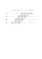
以上は2値の画像データを符号化及び復号化する例について説明したが、次に、複数のビットプレーンで構成される多値画像を画素順序で符号化及び復号化する場合について説明する。画素順序とはプレーン順序と異なり、例えば2ビットプレーンでは図7(a)に示すように、・・・,{i−1}[2],{i−1}[1],{i}[2],{i}[1],{i+1}[2],{i+1}[1],{i+2}[2],・・・({ }[1]は上位ビットプレーン、{ }[2]は下位ビットプレーンを表わす)のように、下位ビットと上位ビットを交互に符号化し、画素を逐次符号化するものである。
【0085】
この時に問題となるのは、各々のプレーンにおいて何を参照してコンテキスト情報とするかいうことである。各々のプレーンを独立に符号化する場合には、上位ビットを符号化する時には上位ビットプレーンだけを、下位ビットを符号化する時には下位ビットプレーンだけを参照すればよい。
【0086】
ところが、下位ビットを符号化する時に上位ビット、それも同一画素の上位ビットを参照したい場合には、上位ビットを下位ビットよりも前に符号化する必要がある。これに対しては、前記符号化順序を図7(b)に示すように、・・・,{i−1}[1],{i−1}[2],{i}[1],{i}[2],{i+1}[1],{i+1}[2],{i+2}[1],・・のように変更すればよい。該符号化順序の変更によって、復号化が可能となる。
【0087】
【発明が解決しようとする課題】
上記従来例による復号化ブロックを用いて、多値画像の複数ビットプレーンを算術復号化しようとすると、ある着目ビットを復号化する時、復号化処理に必要なすべてのコンテキスト情報が確定するのは最悪、直前のビットを復号化してからである。そのため、直前のビットを復号化してからでないと学習メモリを読み出すことができないので、ハードウェアで復号化処理を行なう場合、復号化動作速度を高速化する大きな妨げになっていた。
【0088】
本発明は上記問題点を鑑みてなされたものであり、単純な構成を有するハードウェアで、算術符号化された多値画像の算術復号化速度を高速化することを目的とする。
【0089】
【課題を解決するための手段】
上記目的を達成するために、1画素をmビット(m≧2)で表される多値画像データを、各画素を構成する1ビット毎に算術符号化する本発明の算術符号化/復号化方法は、符号化/復号化対象画素を構成する各符号化/復号化対象ビットを符号化/復号化する為に、2サイクル以上前に符号化/復号化されたビットを用いてコンテキスト情報を生成するコンテキスト生成ステップと、前記符号化/復号化対象ビットを、前記コンテキスト情報に基づいて算術符号化/復号化する算術符号化/復号化ステップとを備え、前記多値画像データを構成するビットプレーンの数をm、該ビットプレーン番号をMSBから順に1、2、・・・mとし、各画素の番号を{ }、ビットプレーンを[ ]で表すとすると、前記算術符号化/復号化するビットの順序として、{i}[j]の次は、j≠mの場合{i‐1}[j+1]を、j=mの場合{i+m}[1]を算術符号化/復号化する。
【0091】
好適な一様態によれば、符号化/復号化する画素の数がnである場合、{i−1}≦0及び{i+1}>nでは、所定値を符号化/復号化する。
【0092】
また、好適な別の一様態によれば、符号化/復号化する画素の数がnである場合、{i−1}≦0及び{i+1}>nでは、符号化/復号化をスキップする。
【0093】
また、上記目的を達成するために、1画素をmビット(m≧2)で表される多値画像データを、各画素を構成する1ビット毎に算術符号化する本発明の算術符号化/復号化装置は、符号化/復号化対象画素を構成する各符号化/復号化対象ビットを符号化/復号化する為に、2サイクル以上前に符号化/復号化されたビットを用いてコンテキスト情報を生成するコンテキスト生成手段と、前記符号化/復号化対象ビットを、前記コンテキスト情報に基づいて算術符号化/復号化する算術符号化/復号化手段とを備え、前記多値画像データを構成するビットプレーンの数をm、該ビットプレーン番号をMSBから順に1、2、・・・mとし、各画素の番号を{ }、ビットプレーンを[ ]で表すとすると、前記算術符号化/復号化するビットの順序として、{i}[j]の次は、j≠mの場合{i‐1}[j+1]を、j=mの場合{i+m}[1]を算術符号化/復号化する。
【0095】
好適な一様態によれば、算術復号化装置は、予測値及び確率推定値を保持する、各ビットプレーン毎に設けられた確率推定値メモリと、前記生成されたコンテキスト情報に基づいて予測値及び確率推定値を更新する予測推定更新手段とを有し、前記生成されたコンテキスト情報をアドレスとして、前記確率推定値メモリから予測値及び確率推定値を読み出す。
【0096】
また、好適な別の一様態によれば、算術復号化装置は、予測値及び状態値を保持する、各ビットプレーン毎に設けられた予測状態メモリと、前記生成されたコンテキスト情報に基づいて予測値及び状態値を更新する予測状態更新手段とを有し、前記生成されたコンテキスト情報をアドレスとして、前記予測状態メモリから予測値及び状態値を読み出す。
【0098】
また、好適な一様態によれば、復号化する画素の数がnである場合、{i−1}≦0及び{i+1}>nでは、所定値を符号化/復号化する。
【0099】
また、好適な別の一様態によれば、復号化する画素の数がnである場合、{i−1}≦0及び{i+1}>nでは、復号化をスキップする。
【0100】
【発明の実施の形態】
以下、添付図面を参照して本発明の好適な実施の形態を詳細に説明する。
【0101】
なお上述の通り、算術符号化方法の種類により使用されている用語が異なるため、本発明の実施の形態においても標準方法であるJBIG方法に用いられている用語を使用するが、これによりJBIG方法の算術符号に限定されるものではない。
【0102】
[第1の実施形態]
本第1の実施形態では、1画素が2ビットからなる多値画像の算術符号化方法と該算術符号化方法に対応する算術復号化装置を示す。
【0103】
図8は、本第1の実施形態における符号化/復号化の順序を表わす図である。同図における矢印の示す順序で算術符号化/復号化をする。すなわち、・・・,{i}[1],{i−1}[2],{i+1}[1],{i}[2],{i+2}[1],{i+1}[2],{i+3}[1],・・・の順序で符号化/復号化する。ここで、{ }[1]は上位ビットプレーンを、{ }[2]は下位ビットプレーンを表わす。
【0104】
1番目の画素の最上位ビット即ち{1}[1]の次は{−1}[2]を符号化/復号化することとなるが、これは存在しない画素の下位ビットにあたる。また、画素数をnとしたとき最後から2番目の画素の下位ビット即ち{n−1}[2]の次は{n+1}[1]を符号化/復号化することとなり、これも存在しない画素である。これらのビットは本来符号化する必要はないが、ダミービットとして例えば0を符号化しておき、復号化時には復号化されたダミービットを捨てて元画像を得てもよい。この方法によれば画像の先端及び終端において例外的な動作を行なわなくても済むので装置構成が簡単になるという利点がある。
【0105】
上位ビットプレーンを符号化する時にはそれ以前に符号化した上位ビットのみを参照する。すなわち、上位ビットプレーンを符号化する時のコンテキスト情報はそれ以前に符号化した上位ビットのみを用いて構成する。
【0106】
下位ビットプレーンを符号化する時にはそれ以前に符号化した下位ビットと、該下位ビット以前に符号化した上位ビットとを参照する。具体的には上記順序で符号化を行う場合、{i}[2]を符号化する時に参照できる下位ビットは{i−1}[2]であり、また上位ビットは、参照する下位ビット{i−1}[2]を符号化する以前に符号化した上位ビット、すなわち{i}[1]以前の上位ビットである。実際的には{i−1}[2]以前の下位ビットの一部と、{i}[1]とを参照する。
【0107】
従来は、復号対象となるビット情報を復号化する1つ前のサイクルで必要なコンテキスト情報が確定していたが、本第1の実施形態では、2つ前のサイクルで必要なコンテキスト情報が確定する。復号化順序は符号化順序とまったく同じであるため、図8に示すように・・・,{i}[1],{i−1}[2],{i+1}[1],{i}[2],{i+2}[1],{i+1}[2],{i+3}[1],・・・の順序で復号化処理が行なわれる。
【0108】
まず、上記復号化順序により、上位ビットプレーンの符号化データを復号する場合について考える。上位ビットの復号化にはそれ以前に符号化した上位ビットのみを参照するため、{i+1}[1]を復号化するのに必要なコンテキスト情報は、{i}[1]及びそれ以前の上位ビット情報である。この場合、{i+1}[1]を復号化するのに必要な一番最後の情報である{i}[1]の復号化は、{i+1}{i}を処理するタイミングに対して2サイクル前に終了している。
【0109】
次に、下位ビットプレーンの符号化データを復号する場合について考える。{i}[2]を符号化する時に参照する上位ビット{i}[1]の復号化は、{i}[2]に対し3サイクル前に終了している。また、下位ビットプレーン上の参照ビットの復号化は2サイクル前に終了している。従って、図8に示す復号化順序では、着目ビットの復号化処理に必要なコンテキスト情報は、いずれのプレーンにおいても2サイクル前には確定していることが解る。
【0110】
上記のように参照ビット情報を用いてコンテキストを生成し、符号化したデータをハードウェアで復号化する方法においては、信号処理のタイミングが大変重要である。この場合は特にコンテキスト情報が確定するタイミングが重要となる。上記復号化順序で復号化処理可能な復号化ブロックの構成について、図9を参照して説明する。
【0111】
同図において、801は上位ビットプレーンを復号化する時のコンテキスト情報、803は上記コンテキスト情報801をラッチするD−F/F、805は下位ビットプレーンを復号化する時のコンテキスト情報、807はコンテキスト情報805をラッチするD−F/F、809は上位ビットプレーンを復号化する時に用いる確率推定値メモリ、811は下位ビットプレーンを復号化する時に用いる確率推定値メモリ、813は上記2つの確率推定値メモリの出力の一方を選択するセレクタ、815はセレクタ813の出力と更新した確率推定値の一方を選択するセレクタ、817はセレクタ815から出力する確率推定値をラッチするD−F/F、819は予測・確率更新部から出力する更新された予測値と確率推定値をラッチするD−F/Fである。なお、その他の構成要素は図6において同一番号で示す要素と同様の機能を有する。
【0112】
上記構成を有する復号化ブロックにおける復号化処理のタイミングを、画素ビット{i+1}[1]から画素ビット{i+3}[1]を処理する場合について、図10を参照して説明する。
【0113】
まず最初のサイクルで、{i+1}[1]に対応する予測値及び確率推定値を確率推定値メモリ809から読み出す。セレクタ813は1サイクル毎に確率推定値メモリ809及び811を交互に選択するように制御されており、ここでは確率推定値メモリ809からの出力を選択する。また、セレクタ815は、図6のセレクタ615と同様に、(読み出しアドレス=書き込みアドレス)かつ(現サイクルの復号画素値=1サイクル前の復号画素値)かつ(メモリ更新時)の条件が成り立つ場合にのみD−F/F819の出力を選択する。従って、通常はスイッチ813の出力を選択している。読み出された予測値及び確率推定値はD−F/F817に一旦ラッチされる。
【0114】
次のサイクル2でD−F/F817にラッチされた予測値及び確率推定値は算術復号化演算部301に入力し、{i+1}[1]の符号化データが算術復号化される。この算術演算の結果、復号した画素値がコンテキスト情報の一部として得られるが、サイクルの後半に確定するので、このコンテキスト情報を安定した信号として使用するために、一度D−F/F803にラッチする。これによりD−F/F803から出力されるコンテキスト情報は1サイクル遅れた信号となるが、サイクルの先頭から安定した信号として使用することができる。
【0115】
また、該確率推定値も同じくサイクルの後半に確定するため、それを安定した信号として使用するためにD−F/F918でラッチする。
【0116】
また、サイクル2の間に、上記処理と平行して{i}[2]に対応する予測値及び確率推定値を確率推定値メモリ811から読み出し、D−F/F817によりラッチする。
【0117】
次のサイクル3で、D−F/F819にラッチされた{i+1}[1]に対する更新予測・確率推定値が正規化処理に対応して確率推定値メモリ809に書き込まれる。同時に、D−F/F817にラッチされた予測値及び確率推定値は算術復号化演算部301に入力し、{i}[2]の符号化データが算術復号化され、復号した画素値をコンテキスト情報の一部として、他の情報と一緒にD−F/F807によりラッチする。
【0118】
また、サイクル3の間に、上記処理と平行して{i+2}[1]に対応する予測値及び確率推定値を確率推定値メモリ809から読み出し、D−F/F817によりラッチする。
【0119】
次のサイクル4では、D−F/F819にラッチされた{i}[2]に対する更新予測・確率推定値が正規化処理に呼応して確率推定値メモリ811に書き込まれる。同時に、D−F/F817にラッチされた予測値及び確率推定値は算術復号化演算部301に入力する。なお、図10に示すように、{i+2}[1]の符号化データを復号化する際に用いられる予測値及び確率推定値はサイクル2で確定した{i+1}[1]のコンテキスト情報に基づく値である。この予測値及び確率推定値を使用して{i+2}[1]は算術復号化され、さらに、予測確率更新部501により得られる更新予測・確率推定値をD−F/F819によりラッチする。
【0120】
また、サイクル4の間に、上記処理と平行して{i+1}[2]に対応する予測値及び確率推定値を確率推定値メモリ811から読み出し、D−F/F817によりラッチする。
【0121】
次のサイクル5では、D−F/F819にラッチされた{i+2}[1]に対応する更新予測・確率推定値が正規化処理に呼応して確率推定値メモリ809に書き込まれる。同時に、D−F/F817にラッチされた予測値及び確率推定値は算術復号化演算部301に入力する。なお、図10に示すように、{i+1}[2]の符号化データを復号化する際に用いられる予測値及び確率推定値は、サイクル2で確定した{i+1}[1]のコンテキスト情報及びサイクル3で確定した{i}[2]のコンテキスト情報に基づく値である。この予測値及び確率推定値を使用して{i+1}[2]は算術復号化され、さらに、予測確率更新部501により得られる更新予測・確率推定値をD−F/F819によりラッチする。
【0122】
また、サイクル5の間に、上記処理と平行して{i+3}[1]に対応する予測値及び確率推定値を確率推定値メモリ809から読み出し、D−F/F817によりラッチする。
【0123】
上記手順による処理を、すべての画素ビットについて繰り返し行う。
【0124】
このように、2サイクル先行していたコンテキスト情報としての復号画素値も、それを一度D−F/F803でラッチし、メモリ読み出し後にもう一度D−F/F817でラッチすることによって、2サイクルの遅れが生じ、最終的には、算術復号化演算部301における位相と一致する。
【0125】
上記の通り本発明の第1の実施形態によれば、多値画像を構成する複数ビットプレーンをプレーン間で数画素ずつずらして符号化する。すなわちあるビットプレーンを符号化する時に、コンテキスト情報として参照する別のビットプレーンを復号化対象画素ビットのビットプレーンより数画素先行して符号化し、復号化時は符号化時と同じ順序で復号化処理を行なうため、ハードウェアで復号化処理を行なう際に、復号化動作速度を大幅に高速化することが可能になる。
【0126】
[第2の実施形態]
本第2の実施形態では、1画素が4ビットからなる多値画像の算術符号化方法と該算術符号化方法に対応する算術復号化装置を示す。
【0127】
図11に本第2の実施形態における符号化復号化順序を表わす図を示す。同図における矢印の示す順序で算術符号化/復号化をする。すなわち、・・・,{i}[1],{i−1}[2],{i−2}[3],{i−3}[4],{i+1}[1],{i}[2],{i−1}[3],{i−2}[4],{i+2}[1],{i+1}[2],{i}[3],{i−1}[4],{i+3}[1],・・・の順序で符号化/復号化をする。ここで、{ }[1]は最上位ビットプレーンを{ }[4]は最下位ビットプレーンを表わす。
【0128】
最上位ビットプレーンを符号化する時にはそれ以前に符号化した最上位ビットのみを参照する。すなわち、最上位ビットプレーンを符号化する時のコンテキスト情報はそれ以前に符号化した最上位ビットのみを用いて構成する。
【0129】
最上位以外のビットプレーンを符号化する時にはそれ以前に符号化した同一プレーンのビットと該ビット以前に符号化した上位のビットを参照する。上記符号化順序の場合、{i}[2]を符号化する時に参照できる同一プレーンのビットは{i−1}[2]であり、また上位ビットは、参照する前記ビット{i−1}[2]を符号化する以前に符号化した上位ビット、すなわち{i}[1]以前の上位ビットである。実際的には{i−1}[2]以前の同一プレーンのビットの一部と、{i}[1]とを参照する。
【0130】
ただし第1実施例と同様、画像の先端と終端付近では存在しない画素のビットを処理するタイミングが発生する。すなわち画像の先端では、{1}[1],{0}[2],{−1}[3],{−2}[4],{2}[1],{1}[2],{0}[3],{−1}[4],{3}[1],{2}[2],{1}[3],{0}[4],{4}[1],{3}[2],{2}[3],{1}[4],という順番で処理を行なうとすると、2番目、3番目、4番目、7番目、8番目、12番目に処理を行うビットは実際には存在しない画素である。第1の実施形態と同様に0のダミービットを符号化しても良いが、本第2の実施形態ではビット情報がないところは符号化を行なわず、復号化時に於いては後述する図12に示す有効画素タイミング発生回路1053とマスク回路1054によって確率推定値を0にしている。確率推定値が0であれば、算術復号化演算部301内のAレジスタ201及びCレジスタ202の値は変化しないので符号化処理を行なわないのと同じことになる。この構成はダミービットを符号化する方法に対して余計な符号を発生させないので符号長を短くできるという利点がある。
【0131】
上記第1の実施形態では、復号対象となるビット情報を復号化するのに必要なコンテキスト情報の2つ前のサイクルで確定していたが、本第2の実施形態では、必要なコンテキスト情報が4つ前のサイクルで確定する。復号化順序は符号化順序とまったく同じであるため、前記・・・,{i}[1],{i−1}[2],{i−2}[3],{i−3}[4],{i+1}[1],{i}[2],{i−1}[3],{i−2}[4],{i+2}[1],{i+1}[2],{i}[3],{i−1}[4],{i+3}[1],・・・の順序で復号化処理が行なわれる。
【0132】
まず、最上位ビットプレーンに着目して考える。最上位ビットの復号化にはそれ以前に符号化した最上位ビットのみを参照するため、{i+1}[1]を復号化するのに必要なコンテキスト情報は、{i}[1]及びそれ以前の最上位ビット情報であり、一番間近の情報である{i}[1]の復号化は{i+1}[1]に対して4サイクル前に終了している。
【0133】
次に、他のビットプレーンについて考える。{i}[j+1]を符号化する時に参照した上位ビット{i}[j]の復号化は、{i}[j+1]に対し5サイクル前に終了している。同一プレーン上の参照ビットは4サイクル前に終了している。従って、着目ビットの復号化処理に必要なコンテキスト情報は、いずれのプレーンにおいても4サイクル前には確定していることが解る。
【0134】
第2の実施形態が、ビットプレーンが2ビットから4ビットへ拡張されたことの他に第1の実施形態と異なる点は、メモリに保持する値としては状態値を用いること、バイパスの経路がないこと、有効画素のみを符号化するための手段が加えられていることである。
【0135】
上記のような参照ビット情報でコンテキストを生成し、符号化したデータをハードウェアで復号化する復号化ブロックの構成について、図12を参照して説明する。
【0136】
同図において、1010は最上位ビットプレーンを復号化する時のコンテキスト情報、1011はコンテキスト情報1010をラッチするD−F/F、1020は2番目に上位のビットプレーンを復号化する時のコンテキスト情報、1021はコンテキスト情報1020をラッチするD−F/F、1030は3番目に上位のビットプレーンを復号化する時のコンテキスト情報、1031はコンテキスト情報1030をラッチするD−F/F、1040は最下位ビットプレーンを復号化する時のコンテキスト情報、1041はコンテキスト情報1040をラッチするD−F/F、1012は最上位ビットプレーンを復号化する時に用いる予測状態メモリ、1022は2番目に上位のビットプレーンを復号化する時に用いる予測状態メモリ、1032は3番目に上位のビットプレーンを復号化する時に用いる予測状態メモリ、1042は最下位ビットプレーンを復号化する時に用いる予測状態メモリ、1050は上記4つの予測状態メモリ1012,1022,1032,1042の出力の一つを選択するセレクタ、1051は上記セレクタから出力する予測状態値をラッチするD−F/F、109は状態値を確率推定値LSZに変換する確率推定部、1053は、有効画素の確率推定値が変換されているとき1を出力する有効画素タイミング発生回路、1054は、無効画素に対応する確率推定値を強制的に0にマスクするマスク回路、1055はマスク回路から出力された確率推定値をラッチするD−F/F、1056は現在の確率推定値から更新時の状態値を予測する予測状態更新部、1057は予測状態の更新値をラッチするD−F/F、1058は復号したビット情報をラッチするD−F/Fである。なお、その他の構成要素は、図6において同一番号で示す要素と同様の機能を有する。
【0137】
状態値をメモリへ保持する構成が可能なのはコンテキストが4サイクル前に確定するので確率推定値を生成するために必要な余計なディレイを許容できるからである。例えば予測状態メモリ1012からある状態値が出力されたとすると、2サイクル後に算術復号化より復号ビット情報が排他的NORゲート305より出力されるので、D−F/F1058によりさらに1サイクル遅延を加えて4サイクル後に次の画素のコンテキストの一部としてD−F/F1011にラッチさせる。状態値は確率推定値よりビット幅が狭いので、メモリの容量を少なくし回路規模を小さくするためには本構成の方が好ましい。
【0138】
メモリへの更新データをバイパスする必要がないのは、各メモリからの読み出しが4サイクルおきであるためである。例えば予測状態メモリ1012からある状態値が出力され、さらに状態値の更新が行なわれるとすれば、その更新値がD−F/F1057にセットされるのは3サイクル後である。つまり3サイクル後にメモリ1012へ更新値の書き込み処理を行なえば、次のサイクルで仮に4サイクル前と同じコンテキストが発生したとしても更新済みの状態値を読み出せる訳である。
【0139】
上記の処理タイミングを示したものが図13である。
【0140】
上記の通り本第2の実施形態によれば、多値画像を構成する複数ビットプレーンをプレーン間で数画素ずつずらして符号化する。すなわちあるビットプレーンを符号化する時に、コンテキスト情報として参照する別のビットプレーンを復号化対象画素ビットのビットプレーンより数画素先行して符号化し、復号化時は符号化時と同じ順序で復号化処理を行なうため、ハードウェアで復号化処理を行なう際に、復号化動作速度を大幅に高速化することが可能になる。
【0141】
なお、本発明は、複数の機器(例えばホストコンピュータ、インタフェイス機器、リーダ、プリンタなど)から構成されるシステムに適用しても、一つの機器からなる装置(例えば、複写機、ファクシミリ装置など)に適用してもよい。
【0142】
【発明の効果】
以上説明したように本発明によれば、単純な構成を有するハードウェアで、算術符号化された多値画像の算術復号化速度を高速化することができる。
【図面の簡単な説明】
【図1】従来の算術符号化処理を行なう符号化ブロックの構成を示すブロック図である。
【図2】図1に示す算術符号化演算部の構成例を示すブロック図である。
【図3】従来の算術復号化処理を行なう復号化ブロックの構成を示すブロック図である。
【図4】図3に示す算術復号化演算部の構成例を示すブロック図である。
【図5】従来の算術復号化処理を行なう復号化ブロックの別の構成を示すブロック図である。
【図6】従来の算術復号化処理を行なう復号化ブロックの別の構成を示すブロック図である。
【図7】従来の符号化/復号化の順序を表わす図である。
【図8】本発明の第1の実施形態における符号化/復号化の順序を表わす図である。
【図9】本発明の第1の実施形態における算術復号化処理を行なう復号化ブロックの構成を示すブロック図である。
【図10】図9に示す復号化ブロックにより復号化を行う際の処理タイミングを示す図である。
【図11】本発明の第2の実施形態における符号化/復号化の順序を表わす図である。
【図12】本発明の第2の実施形態における算術復号化処理を行なう復号化ブロックの構成を示すブロック図である。
【図13】図12に示す復号化ブロックにより復号化を行う際の処理タイミングを示す図である。
【符号の説明】
101 端子
102 2値データPIX信号
103 コンテキスト情報
105 予測状態メモリ
106 予測値
107 状態値
109 確率推定部
111 確率推定値LSZ
113 排他的NORゲート
114 一致/不一致信号
115 算術符号化演算部
117 符号化データ
118 信号
119 予測状態更新部
120 制御信号
201 Aレジスタ
203 コードレジスタ
205 減算器
207 加算器
209 セレクタ
211 セレクタ
213 シフトレジスタ
215 出力レジスタ
217 カウンタ
218 端子
219 マスク回路
220 シフトクロック
221 検出器
301 算術復号化演算部
302 信号
304 復号画素値信号
305 排他的NORゲート
306 符号化データ
401 減算器
403 入力バッファレジスタ
405 シフトレジスタ
501 予測確率更新部
503 確率推定値メモリ
601 第1の確率推定値メモリ
602 第2の確率推定値メモリ
603、605 セレクタ
607 D−F/F
609 遅延回路
610 コンテキスト情報
801、805 コンテキスト情報
803、807、817、819 D−F/F
809、811 確率推定値メモリ
813、815 セレクタ
1010、1020、1030、1040 コンテキスト情報
1011、1021、1031、1041 D−F/F
1012、1022、1032、1042 予測状態メモリ
1050 セレクタ
1051、1055、1057、1058 D−F/F
1053 有効画素タイミング発生回路
1054 マスク回路
1056 予測状態更新部[0001]
BACKGROUND OF THE INVENTION
The present invention relates to an arithmetic encoding method that encodes image data using an arithmetic code, and an arithmetic decoding device that decodes image data encoded by the method, and more particularly, arithmetic of a multi-valued image. The present invention relates to an encoding method and an arithmetic decoding device.
[0002]
[Prior art]
Arithmetic codes are inequalities corresponding to the occurrence probability of each symbol in a corresponding interval (binary decimal [0.0... 0, 0.1... 1]) on a numerical line of [0, 1). The coordinates of the points included in the section obtained by dividing into long segments, assigning the encoding target symbol series to the corresponding partial sections, and repeating the division recursively can be distinguished from at least
[0003]
Typical arithmetic coding methods include JBIG (QM-coder) method standardized by JBIG (Joint Bi-1vel Image Experts Group), which is an ITU organization, and Q-coder proposed by IBM Corporation. is there.
[0004]
Since the terminology used in each method is different, the terminology used in the standard method JBIG method is used here, but is not limited to the arithmetic code of the JBIG method.
[0005]
Arithmetic coding, in principle, requires a multiplication process in the arithmetic operation unit. However, when the multiplication process is performed, there is a problem that the hardware scale of the arithmetic operation unit increases or the processing time required for the multiplication process increases. For this reason, a simplified method is widely used by replacing the arithmetic operation with an addition / subtraction operation.
[0006]
In the arithmetic operation unit, there are an A register that holds a region width (orient) corresponding to an encoded symbol sequence, and a code register (C register) that holds a value that is a basis for generating a code. The probability of loss of the encoding target symbol with respect to the predicted value is input as a probability estimated value LSZ, and the arithmetic operation is performed based on the probability estimated value LSZ and the values of the two registers based on information indicating whether the symbol matches or does not match the predicted value. An operation (addition / subtraction) is performed to update the values of the two registers.
[0007]
The probability estimated value LSZ is obtained by converting from the index (state) value for each context obtained by digitizing the peripheral symbol information of the encoding target symbol using a predetermined correspondence table. By updating the state value of each context based on a predetermined condition, it is possible to learn a pattern specific to the encoded symbol sequence and increase the encoding efficiency.
[0008]
In the JBIG method, the value of the A register is initialized to 10000H, and when the value of the A register becomes less than 8000H as a result of the arithmetic operation (encoding or decoding), the value of the A register is 8000H or more. Shift to the left until the current state value is updated.
[0009]
Further, when the value of the A register is shifted to the left, the value of the C register is also shifted to the left at the same time. At this time, the data shifted out from the upper part of the C register becomes the encoded data.
[0010]
In the case of binary pixel data in which the value of the symbol to be encoded is only 0 or 1, the configuration of the encoding block for performing the arithmetic encoding process is as shown in FIG.
[0011]
<Encoding block>
In the figure, 101 is a terminal for inputting binary data PIX of the encoding target pixel, 102 is a binary data PIX signal, 103 is context information composed of peripheral pixel data of the encoding target pixel, and 105 is predicted for each context information. Prediction state memory that holds a value and an index (state) value, 106 is a prediction value output from the
[0012]
Next, the operation of the arithmetic coding processing block shown in FIG. 1 will be described.
[0013]
The binary data PIX of the encoding target pixel is input from the
[0014]
The
[0015]
On the other hand, the state value 107 is sent to the
[0016]
The
[0017]
The arithmetic
[0018]
When the normalization process described above is performed in the course of the arithmetic operation in the arithmetic
[0019]
The predicted
[0020]
Next, FIG. 2 shows a configuration example of the arithmetic
[0021]
In the figure, 201 is an A register that holds an area width (orient), 203 is a code register (C register) that holds a value that is a basis for generating a code, and 205 is a probability estimate from an output value of the
[0022]
In the state after initialization, the value of the
[0023]
By performing a predetermined arithmetic operation based on the inputted match /
[0024]
First, the input
[0025]
The
[0026]
A
[0027]
The
[0028]
The outputs of the
[0029]
When the value of the
[0030]
One realization method of the normalization process uses a register having a shift function for each of the
[0031]
The
[0032]
While the value of the
[0033]
Since the data input to the
[0034]
The number of bits transferred to the
[0035]
The
[0036]
When the
[0037]
By the arithmetic operation and normalization processing as described above, the binary data PIX input to the terminal 101 is encoded, and the encoded
[0038]
<Decryption block>
Next, the configuration of a decoding block corresponding to the coding block shown in FIG. 1 is shown in FIG. 3, and its operation will be described.
[0039]
The major differences between the decoding block shown in FIG. 3 and the coding block shown in FIG. 1 are the following two points.
[0040]
(1) Instead of the arithmetic
Since the other configurations are basically the same, the above differences will be briefly described.
[0041]
First, the operation in the arithmetic
[0042]
In the figure, a
[0043]
The input
[0044]
In the arithmetic
[0045]
The
[0046]
With this
[0047]
The
[0048]
The outputs of the
[0049]
The arithmetic
[0050]
The encoded
[0051]
The encoded
[0052]
As a result of the arithmetic processing of the arithmetic
[0053]
In the decoding block, similarly to the encoding block, the
[0054]
The predicted
[0055]
The operation of the other blocks is the same as that of the encoding block in FIG.
[0056]
Next, FIG. 5 shows the configuration of an arithmetic decoding block having means for obtaining an updated probability estimate from a probability estimate described in Japanese Patent Laid-Open No. 11-103257 proposed by the present inventor. In FIG. 5,
[0057]
Comparing the configuration diagram of FIG. 5 with the configuration diagram of FIG. 3, it can be seen that there is no
[0058]
Since the input / output signals of the arithmetic
[0059]
The
[0060]
In order to store the probability estimation value in the probability
[0061]
The updated probability estimation value is obtained by the prediction
[0062]
Therefore, in the decoding block having the above configuration, the state value 107 does not physically exist. However, the conversion table (necessary for creating the ROM table or decoder) from the current probability estimate to the updated probability estimate is created by replacing the transition of the state value with the transition of the probability estimate. It will be included in the table.
[0063]
The status value number is unique. That is, different state value numbers are always assigned to different states. However, the probability estimate is not unique. That is, it is theoretically possible to assign the same probability estimate to different states. However, in the JBIG method, since different probability estimates are assigned to different states, it can be said that the probability estimates are unique if limited to the JBIG method.
[0064]
If the probability estimation value is unique, there is no problem in the processing performed by the prediction
[0065]
The main processing required to encode / decode one pixel in the encoding / decoding block having the configuration shown in FIGS. 1 and 3 is the following four steps.
[0066]
(1) Read predicted value and state value from memory.
(2) Convert the state value into a probability estimate.
(3) Perform arithmetic coding / decoding operations using the probability estimate.
(4) Update the predicted value and state value and write them to the memory (necessary only during normalization processing). Since the update process of the predicted value and the state value in (4) can be performed in parallel with the arithmetic coding operation in (3), the process performed in (4) is only the process of writing to the memory in terms of timing. .
[0067]
In contrast, the decoding block having the configuration shown in FIG.
[0068]
(1) The predicted value and the estimated probability value are read from the memory.
(2) An arithmetic decoding operation is performed using the probability estimation value.
(3) Update the predicted value and the estimated probability value and write them to the memory (necessary only during normalization processing).
Therefore, as compared with the configuration shown in FIGS. 1 and 3, encoding can be performed faster by a time corresponding to the process of converting the state value into the probability estimation value.
[0069]
Further, the present inventor has further proposed an arithmetic decoding block having a configuration as shown in FIG. 6 according to Japanese Patent Laid-Open No. 11-103257.
[0070]
In general, as the context information on which the predicted value is obtained, the pixels immediately above and to the left that have a strong correlation with the target pixel are used. Therefore, when decoding processing is performed in the raster scanning order, If the decoding of (2) is not completed, a prediction value or the like necessary for decoding the pixel on the right side cannot be read out.
[0071]
Therefore, the memory storing the predicted values and the like is divided into a plurality of memory groups, and the plurality of predicted values and the like are read from the memory groups in parallel. The plurality of prediction values correspond to the case where the pixel value of interest during decoding is 0 and 1, respectively, and when the pixel value of interest is determined, one prediction value is selected from the plurality of prediction values. That's it.
[0072]
FIG. 6 shows an arithmetic decoding block having the above memory configuration and storing probability estimates in the memory.
[0073]
In the figure, 601 is a first probability estimated value memory, 602 is a second probability estimated value memory, 603 is a selector for selecting one of the two sets of predicted values / probability estimated values read from the two memories, 605 Is a selector that selects one of the output of the
[0074]
In the configuration of FIG. 6, since the predicted value and the estimated probability value are read out from the memory in advance, the context information for reading the memory and the context information for writing the memory used when the memory is updated are shifted by one cycle, and are sent to different signals. Become. Therefore, it is assumed that a 2-port memory capable of inputting two context information (addresses) at the same time is used.
[0075]
The signal 610 is other context information excluding the target pixel value during the decoding process, and has less 1-bit information than the context information 103 that has been output so far. The context information 610 is given to the first and second probability estimated
[0076]
The first probability estimated
[0077]
From the first and second probability estimated
[0078]
In parallel with the reading from the memory, the target pixel is decoded (arithmetic decoding), and the decoded pixel value is determined when the memory read data is determined. Based on this decoded pixel value, the
[0079]
The output of the
[0080]
This is a case where all context information from which the predicted value / probability estimated value is read and selected and all context information used at the time of memory update completely match. This is paraphrased by the conditions of (read address = write address) and (decoded pixel value of the current cycle = decoded pixel value of one cycle before) and (when updating the memory).
[0081]
When it is detected by a detector (not shown) that the above condition is satisfied, the
[0082]
During the arithmetic operation, new probability estimates are read out from the two
[0083]
In the above configuration, since arithmetic operations for decoding and reading from the probability estimated
[0084]
The example of encoding and decoding binary image data has been described above. Next, a case of encoding and decoding a multi-value image composed of a plurality of bit planes in pixel order will be described. The pixel order is different from the plane order. For example, in the 2-bit plane, as shown in FIG. 7A,..., {I−1} [2], {i−1} [1], {i} [ 2], {i} [1], {i + 1} [2], {i + 1} [1], {i + 2} [2], ... ({} [1] is the upper bit plane, {} [2] The lower bits and the upper bits are alternately encoded, and the pixels are sequentially encoded.
[0085]
The problem at this time is what is referred to as context information in each plane. When encoding each plane independently, it is only necessary to refer to the upper bit plane when encoding the upper bits and only the lower bit plane when encoding the lower bits.
[0086]
However, when it is desired to refer to the upper bit when encoding the lower bit, and also to the upper bit of the same pixel, it is necessary to encode the upper bit before the lower bit. For this, as shown in FIG. 7B, the encoding order is as follows: {i-1} [1], {i-1} [2], {i} [1], {I} [2], {i + 1} [1], {i + 1} [2], {i + 2} [1],... Decoding is enabled by changing the coding order.
[0087]
[Problems to be solved by the invention]
When the decoding block according to the above conventional example is used to perform arithmetic decoding of a plurality of bit planes of a multi-valued image, when decoding a certain bit of interest, all context information necessary for the decoding process is determined. In the worst case, the previous bit is decoded. For this reason, the learning memory can be read only after the previous bit is decoded. Therefore, when the decoding process is performed by hardware, the decoding operation speed is greatly hindered.
[0088]
The present invention has been made in view of the above problems, and is hardware having a simple configuration. arithmetic Encoded multi-valued image arithmetic The purpose is to increase the decoding speed.
[0089]
[Means for Solving the Problems]
To achieve the above objective, The arithmetic coding / decoding method according to the present invention for performing arithmetic coding of multi-value image data in which one pixel is represented by m bits (m ≧ 2) for each bit constituting each pixel is encoded / decoded. A context generating step of generating context information using bits encoded / decoded two cycles or more before in order to encode / decode each encoding / decoding target bit constituting the target pixel; An arithmetic encoding / decoding step for arithmetically encoding / decoding the encoding / decoding target bits based on the context information, wherein m is the number of bit planes constituting the multi-valued image data If the plane number is 1, 2,... M in order from the MSB, the number of each pixel is {}, and the bit plane is represented by [], the order of the bits to be arithmetically encoded / decoded is {i} [J] The following is a case of j ≠ m {i-1} [j + 1], to the arithmetic coding / decoding the {i + m} [1] For j = m .
[0091]
According to a preferred embodiment, when the number of pixels to be encoded / decoded is n, a predetermined value is encoded / decoded when {i−1} ≦ 0 and {i + 1}> n.
[0092]
According to another preferred embodiment, when the number of pixels to be encoded / decoded is n, encoding / decoding is skipped when {i−1} ≦ 0 and {i + 1}> n. .
[0093]
In order to achieve the above purpose, Multi-valued image data in which one pixel is represented by m bits (m ≧ 2) is arithmetically encoded for each bit constituting each pixel. Arithmetic coding of the present invention /Decryption The device Context in which context information is generated by using bits encoded / decoded two cycles or more before in order to encode / decode each encoding / decoding target bit constituting the encoding / decoding target pixel A number of bit planes constituting the multi-value image data, comprising: generating means; and arithmetic coding / decoding means for arithmetically coding / decoding the encoding / decoding target bits based on the context information Where m is the bit plane number, 1, 2,... M in order from the MSB, the number of each pixel is {}, and the bit plane is represented by [], the order of the bits to be arithmetically encoded / decoded. Next, {i} [j] is arithmetically encoded / decoded {i−1} [j + 1] when j ≠ m, and {i + m} [1] when j = m. .
[0095]
According to a preferred embodiment, The arithmetic decoding device A probability estimation value memory provided for each bit plane that holds a prediction value and a probability estimation value; and Generated Prediction estimation update means for updating the prediction value and the probability estimation value based on the context information, and Generated Using the context information as an address, a prediction value and a probability estimation value are read from the probability estimation value memory.
[0096]
Also, according to another preferred embodiment, The arithmetic decoding device A prediction state memory provided for each bit plane that holds a prediction value and a state value; and Generated Prediction state update means for updating the prediction value and the state value based on the context information, and Generated Using the context information as an address, the predicted value and state value are read from the predicted state memory.
[0098]
According to a preferred embodiment, when the number of pixels to be decoded is n, a predetermined value is encoded / decoded when {i−1} ≦ 0 and {i + 1}> n.
[0099]
According to another preferred embodiment, when the number of pixels to be decoded is n, decoding is skipped when {i−1} ≦ 0 and {i + 1}> n.
[0100]
DETAILED DESCRIPTION OF THE INVENTION
Preferred embodiments of the present invention will be described below in detail with reference to the accompanying drawings.
[0101]
As described above, since the terminology used differs depending on the type of arithmetic coding method, the terminology used in the JBIG method which is the standard method is also used in the embodiment of the present invention. It is not limited to the arithmetic sign of.
[0102]
[First Embodiment]
In the first embodiment, an arithmetic coding method of a multi-value image in which one pixel is composed of 2 bits and an arithmetic decoding device corresponding to the arithmetic coding method are shown.
[0103]
FIG. 8 is a diagram showing the order of encoding / decoding in the first embodiment. Arithmetic encoding / decoding is performed in the order indicated by the arrows in FIG. That is, ..., {i} [1], {i-1} [2], {i + 1} [1], {i} [2], {i + 2} [1], {i + 1} [2], Encoding / decoding is performed in the order of {i + 3} [1],. Here, {} [1] represents an upper bit plane and {} [2] represents a lower bit plane.
[0104]
Next to the most significant bit of the first pixel, that is, {1} [1], {−1} [2] is encoded / decoded, which corresponds to the low-order bit of a nonexistent pixel. When n is the number of pixels, the least significant bit of the second pixel from the end, that is, {n−1} [2] is followed by encoding / decoding {n + 1} [1], which does not exist. Pixel. These bits do not have to be encoded originally, but for example, 0 may be encoded as dummy bits, and the decoded dummy bits may be discarded during decoding to obtain the original image. According to this method, there is an advantage that the apparatus configuration is simplified because it is not necessary to perform an exceptional operation at the leading edge and the trailing edge of the image.
[0105]
When encoding the upper bit plane, only the upper bits encoded before that are referred to. That is, the context information when encoding the upper bit plane is configured using only the upper bits encoded before.
[0106]
When the lower bit plane is encoded, the lower bit encoded before that and the upper bit encoded before the lower bit are referred to. Specifically, when encoding is performed in the above order, the lower bit that can be referred to when {i} [2] is encoded is {i−1} [2], and the upper bit is the lower bit to be referenced { i-1} [2] is an upper bit encoded before encoding, that is, an upper bit before {i} [1]. Actually, a part of the lower bits before {i−1} [2] and {i} [1] are referred to.
[0107]
Conventionally, the necessary context information is determined in the previous cycle for decoding the bit information to be decoded. In the first embodiment, the required context information is determined in the previous two cycles. To do. Since the decoding order is exactly the same as the encoding order, as shown in FIG. 8,..., {I} [1], {i−1} [2], {i + 1} [1], {i} Decoding processing is performed in the order of [2], {i + 2} [1], {i + 1} [2], {i + 3} [1],.
[0108]
First, consider the case where the encoded data of the upper bit plane is decoded in the above decoding order. Since only the high-order bits encoded before that are referred to for decoding the high-order bits, the context information necessary for decoding {i + 1} [1] is {i} [1] and the high-order bits before that Bit information. In this case, decoding of {i} [1], which is the last information necessary for decoding {i + 1} [1], takes two cycles with respect to the timing of processing {i + 1} {i}. Has ended before.
[0109]
Next, consider the case of decoding the encoded data of the lower bit plane. Decoding of the upper bits {i} [1] to be referred to when {i} [2] is encoded is completed three cycles before {i} [2]. Also, the decoding of the reference bits on the lower bit plane has been completed two cycles ago. Therefore, in the decoding order shown in FIG. 8, it can be seen that the context information necessary for the decoding process of the bit of interest is determined two cycles before in any plane.
[0110]
In the method of generating a context using the reference bit information as described above and decoding the encoded data by hardware, the timing of signal processing is very important. In this case, the timing for determining the context information is particularly important. The configuration of a decoding block that can be decoded in the decoding order will be described with reference to FIG.
[0111]
In the figure, 801 is context information for decoding the upper bit plane, 803 is a DF / F that latches the
[0112]
The timing of the decoding process in the decoding block having the above configuration will be described with reference to FIG. 10 in the case of processing pixel bits {i + 1} [1] to pixel bits {i + 3} [1].
[0113]
First, in the first cycle, a prediction value and a probability estimation value corresponding to {i + 1} [1] are read from the probability
[0114]
The prediction value and the probability estimation value latched by the DF /
[0115]
Further, since the probability estimation value is also determined in the second half of the cycle, it is latched by the DF / F 918 to use it as a stable signal.
[0116]
Also, during
[0117]
In the
[0118]
Further, during
[0119]
In the
[0120]
Further, during
[0121]
In the
[0122]
Also, during
[0123]
The process according to the above procedure is repeated for all pixel bits.
[0124]
In this way, the decoded pixel value as the context information that preceded two cycles is also delayed by two cycles by latching it once with the DF /
[0125]
As described above, according to the first embodiment of the present invention, encoding is performed by shifting a plurality of bit planes constituting a multi-value image by several pixels between planes. In other words, when encoding a bit plane, another bit plane that is referred to as context information is encoded several pixels ahead of the bit plane of the pixel bit to be decoded, and the decoding is performed in the same order as the encoding. Since the process is performed, the decoding operation speed can be greatly increased when the decoding process is performed by hardware.
[0126]
[Second Embodiment]
In the second embodiment, an arithmetic coding method of a multi-value image in which one pixel is composed of 4 bits and an arithmetic decoding device corresponding to the arithmetic coding method are shown.
[0127]
FIG. 11 is a diagram showing the encoding / decoding order in the second embodiment. Arithmetic encoding / decoding is performed in the order indicated by the arrows in FIG. That is, ..., {i} [1], {i-1} [2], {i-2} [3], {i-3} [4], {i + 1} [1], {i} [2], {i-1} [3], {i-2} [4], {i + 2} [1], {i + 1} [2], {i} [3], {i-1} [4 ], {I + 3} [1],... Here, {} [1] represents the most significant bit plane and {} [4] represents the least significant bit plane.
[0128]
When encoding the most significant bit plane, only the most significant bit encoded before is referred. That is, the context information when encoding the most significant bit plane is configured using only the most significant bits encoded before.
[0129]
When encoding a bit plane other than the most significant bit plane, reference is made to the bits of the same plane encoded before that and the upper bits encoded before that bit. In the case of the above encoding order, the bit of the same plane that can be referred to when {i} [2] is encoded is {i−1} [2], and the upper bit is the bit {i−1} to be referred to. Upper bits encoded before [2] is encoded, that is, upper bits before {i} [1]. Actually, a part of bits of the same plane before {i−1} [2] and {i} [1] are referred to.
[0130]
However, as in the first embodiment, a timing for processing a bit of a pixel that does not exist in the vicinity of the leading edge and the trailing edge of the image occurs. That is, at the leading edge of the image, {1} [1], {0} [2], {-1} [3], {-2} [4], {2} [1], {1} [2], {0} [3], {−1} [4], {3} [1], {2} [2], {1} [3], {0} [4], {4} [1], If processing is performed in the order {3} [2], {2} [3], {1} [4], the processing is performed in the second, third, fourth, seventh, eighth, and twelfth. The bits to be performed are pixels that do not actually exist. As in the first embodiment, 0 dummy bits may be encoded. However, in the second embodiment, no coding is performed where there is no bit information. The probability estimation value is set to 0 by the effective pixel
[0131]
In the first embodiment, the information is determined in a cycle two times before the context information necessary for decoding the bit information to be decoded. In the second embodiment, the necessary context information is Confirm in the previous 4 cycles. Since the decoding order is exactly the same as the encoding order, the above-mentioned, {i} [1], {i-1} [2], {i-2} [3], {i-3} [ 4], {i + 1} [1], {i} [2], {i-1} [3], {i-2} [4], {i + 2} [1], {i + 1} [2], { Decoding processing is performed in the order of i} [3], {i−1} [4], {i + 3} [1],.
[0132]
First, consider the most significant bit plane. Since only the most significant bit encoded before is referred to for decoding the most significant bit, the context information necessary for decoding {i + 1} [1] is {i} [1] and earlier The decoding of {i} [1], which is the most significant bit information and the closest information, is completed four cycles before {i + 1} [1].
[0133]
Next, consider another bit plane. Decoding of the upper bits {i} [j] referred to when {i} [j + 1] is encoded is completed five cycles before {i} [j + 1]. Reference bits on the same plane are completed 4 cycles ago. Therefore, it can be seen that the context information necessary for the decoding process of the bit of interest is fixed 4 cycles before in any plane.
[0134]
The second embodiment is different from the first embodiment except that the bit plane is expanded from 2 bits to 4 bits. The second embodiment is different from the first embodiment in that a state value is used as a value held in a memory and a bypass path is No means are added to encode only the effective pixels.
[0135]
A configuration of a decoding block that generates a context using the reference bit information as described above and decodes the encoded data by hardware will be described with reference to FIG.
[0136]
In the figure, 1010 is context information for decoding the most significant bit plane, 1011 is a DF / F that latches the
[0137]
The configuration in which the state value is held in the memory is possible because the context is determined four cycles ago, so that an extra delay necessary for generating the probability estimate can be allowed. For example, if a certain state value is output from the
[0138]
The reason why it is not necessary to bypass the update data to the memory is that reading from each memory is performed every four cycles. For example, if a certain state value is output from the predicted
[0139]
FIG. 13 shows the above processing timing.
[0140]
As described above, according to the second embodiment, encoding is performed by shifting a plurality of bit planes constituting a multilevel image by several pixels between planes. In other words, when encoding a bit plane, another bit plane that is referred to as context information is encoded several pixels ahead of the bit plane of the pixel bit to be decoded, and the decoding is performed in the same order as the encoding. Since the process is performed, the decoding operation speed can be greatly increased when the decoding process is performed by hardware.
[0141]
Note that the present invention can be applied to a system including a plurality of devices (for example, a host computer, an interface device, a reader, and a printer), and a device (for example, a copying machine and a facsimile device) including a single device. You may apply to.
[0142]
【The invention's effect】
As described above, according to the present invention, with hardware having a simple configuration, arithmetic Encoded multi-valued image arithmetic The decoding speed can be increased.
[Brief description of the drawings]
FIG. 1 is a block diagram showing a configuration of a coding block that performs conventional arithmetic coding processing.
FIG. 2 is a block diagram illustrating a configuration example of an arithmetic coding operation unit illustrated in FIG.
FIG. 3 is a block diagram showing a configuration of a decoding block for performing a conventional arithmetic decoding process.
4 is a block diagram illustrating a configuration example of an arithmetic decoding operation unit illustrated in FIG. 3;
FIG. 5 is a block diagram showing another configuration of a decoding block for performing conventional arithmetic decoding processing.
FIG. 6 is a block diagram showing another configuration of a decoding block for performing conventional arithmetic decoding processing.
FIG. 7 is a diagram illustrating a conventional encoding / decoding order.
FIG. 8 is a diagram illustrating an encoding / decoding order according to the first embodiment of the present invention.
FIG. 9 is a block diagram illustrating a configuration of a decoding block that performs arithmetic decoding processing according to the first embodiment of the present invention.
FIG. 10 is a diagram showing processing timing when decoding is performed by the decoding block shown in FIG. 9;
FIG. 11 is a diagram illustrating an encoding / decoding order according to the second embodiment of the present invention.
FIG. 12 is a block diagram illustrating a configuration of a decoding block that performs arithmetic decoding processing according to the second embodiment of the present invention.
FIG. 13 is a diagram showing processing timing when decoding is performed by the decoding block shown in FIG.
[Explanation of symbols]
101 terminals
102 Binary data PIX signal
103 Context information
105 Predictive state memory
106 predicted value
107 Status value
109 Probability estimation unit
111 Probability estimate LSZ
113 Exclusive NOR gate
114 Match / mismatch signal
115 Arithmetic coding operation part
117 encoded data
118 signals
119 prediction state update unit
120 Control signal
201 A register
203 Code register
205 Subtractor
207 Adder
209 Selector
211 selector
213 Shift register
215 Output register
217 counter
218 terminal
219 Mask circuit
220 shift clock
221 detector
301 Arithmetic decoding operation part
302 signal
304 Decoded pixel value signal
305 Exclusive NOR gate
306 Encoded data
401 Subtractor
403 Input buffer register
405 shift register
501 Prediction probability update unit
503 Probability estimate memory
601 First probability estimation value memory
602 Second probability estimate memory
603, 605 selector
607 DF / F
609 delay circuit
610 Context information
801, 805 context information
803, 807, 817, 819 DF / F
809, 811 probability estimate memory
813, 815 selector
1010, 1020, 1030, 1040 Context information
1011, 1021, 1031, 1041 DF / F
1012, 1022, 1032, 1042 Prediction state memory
1050 selector
1051, 1055, 1057, 1058 DF / F
1053 Effective pixel timing generation circuit
1054 mask circuit
1056 prediction state update unit
Claims (12)
符号化対象画素を構成する各符号化対象ビットを符号化する為に、2サイクル以上前に符号化されたビットを用いてコンテキスト情報を生成するコンテキスト生成ステップと、
前記符号化対象ビットを、前記コンテキスト情報に基づいて算術符号化する算術符号化ステップとを備え、
前記多値画像データを構成するビットプレーンの数をm、該ビットプレーン番号をMSBから順に1、2、・・・mとし、各画素の番号を{ }、ビットプレーンを[ ]で表すとすると、前記算術符号化するビットの順序として、{i}[j]の次は、j≠mの場合{i‐1}[j+1]を、j=mの場合{i+m}[1]を算術符号化することを特徴とする算術符号化方法。 An arithmetic encoding method that arithmetically encodes multi-value image data in which one pixel is represented by m bits (m ≧ 2) for each bit constituting each pixel,
A context generation step for generating context information using bits encoded two or more cycles before encoding each encoding target bit constituting the encoding target pixel;
An arithmetic encoding step for arithmetically encoding the encoding target bit based on the context information,
If the number of bit planes constituting the multi-valued image data is m , the bit plane numbers are 1, 2,... M in order from the MSB, the number of each pixel is {}, and the bit plane is represented by []. , as the order of bits the arithmetic coding, the next {i} [j] is, j ≠ case of m an {i-1} [j + 1], the arithmetic in the case of j = m {i + m} [1] arithmetic coding wherein to encode.
復号化対象画素を構成する各復号化対象ビットを復号化する為に、2サイクル以上前に復号化されたビットを用いてコンテキスト情報を生成するコンテキスト生成ステップと、
前記復号化対象ビットを、前記コンテキスト情報に基づいて算術復号化する算術復号化ステップとを備え、
前記多値画像データを構成するビットプレーンの数をm、該ビットプレーン番号をMSBから順に1、2、・・・mとし、各画素の番号を{ }、ビットプレーンを[ ]で表すとすると、前記算術復号化するビットの順序として、{i}[j]の次は、j≠mの場合{i‐1}[j+1]を、j=mの場合{i+m}[1]を算術復号化することを特徴とする算術復号化方法。 An arithmetic decoding method for arithmetically decoding multi-valued image data in which one pixel is represented by m bits (m ≧ 2) for each bit constituting each pixel,
A context generating step for generating context information using bits decoded two or more cycles before in order to decode each decoding target bit constituting the decoding target pixel;
An arithmetic decoding step of arithmetically decoding the decoding target bits based on the context information,
If the number of bit planes constituting the multi-valued image data is m , the bit plane numbers are 1, 2,... M in order from the MSB, the number of each pixel is {}, and the bit plane is represented by []. , as the order of bits the arithmetic decoding, the next {i} [j] is, j ≠ case of m an {i-1} [j + 1], the arithmetic in the case of j = m {i + m} [1] arithmetic decoding method characterized by decoding.
符号化対象画素を構成する各符号化対象ビットを符号化する為に、2サイクル以上前に符号化されたビットを用いてコンテキスト情報を生成するコンテキスト生成手段と、Context generating means for generating context information using bits encoded two or more cycles ago in order to encode each encoding target bit constituting the encoding target pixel;
前記符号化対象ビットを、前記コンテキスト情報に基づいて算術符号化する算術符号化手段とを備え、Arithmetic encoding means for arithmetically encoding the encoding target bit based on the context information,
前記多値画像データを構成するビットプレーンの数をm、該ビットプレーン番号をMSBから順に1、2、・・・mとし、各画素の番号を{ }、ビットプレーンを[ ]で表すとすると、前記算術符号化するビットの順序として、{i}[j]の次は、j≠mの場合{i‐1}[j+1]を、j=mの場合{i+m}[1]を算術符号化することを特徴とする算術符号化装置。If the number of bit planes constituting the multi-value image data is m, the bit plane numbers are 1, 2,... M in order from the MSB, the number of each pixel is {}, and the bit plane is represented by []. As the order of the bits to be arithmetically encoded, the next to {i} [j] is {i−1} [j + 1] when j ≠ m, and {i + m} [1] when j = m. An arithmetic coding apparatus characterized by comprising:
復号化対象画素を構成する各復号化対象ビットを復号化する為に、2サイクル以上前に復号化されたビットを用いてコンテキスト情報を生成するコンテキスト生成手段と、Context generating means for generating context information using bits decoded two or more cycles before decoding each decoding target bit constituting the decoding target pixel;
前記復号化対象ビットを、前記コンテキスト情報に基づいて算術復号化する算術復号化手段とを備え、Arithmetic decoding means for arithmetically decoding the decoding target bit based on the context information,
前記多値画像データを構成するビットプレーンの数をm、該ビットプレーン番号をMSBから順に1、2、・・・mとし、各画素の番号を{ }、ビットプレーンを[ ]で表すとすると、前記算術復号化するビットの順序として、{i}[j]の次は、j≠mの場合{i‐1}[j+1]を、j=mの場合{i+m}[1]を算術復号化することを特徴とする算術復号化装置。If the number of bit planes constituting the multi-value image data is m, the bit plane numbers are 1, 2,... M in order from the MSB, the number of each pixel is {}, and the bit plane is represented by []. As the order of bits to be arithmetically decoded, {i} [j] is next to {i−1} [j + 1] when j ≠ m, and {i + m} [1] when j = m. An arithmetic decoding device characterized by comprising:
前記生成されたコンテキスト情報に基づいて予測値及び確率推定値を更新する予測推定更新手段とを有し、
前記生成されたコンテキスト情報をアドレスとして、前記確率推定値メモリから予測値及び確率推定値を読み出すことを特徴とする請求項8に記載の算術復号化装置。A probability estimate memory provided for each bit plane that holds the predicted value and the probability estimate;
Prediction estimation update means for updating a prediction value and a probability estimation value based on the generated context information,
9. The arithmetic decoding apparatus according to claim 8 , wherein a prediction value and a probability estimation value are read from the probability estimation value memory using the generated context information as an address.
前記生成されたコンテキスト情報に基づいて予測値及び状態値を更新する予測状態更新手段とを有し、
前記生成されたコンテキスト情報をアドレスとして、前記予測状態メモリから予測値及び状態値を読み出すことを特徴とする請求項8に記載の算術復号化装置。A prediction state memory provided for each bit plane that holds a prediction value and a state value;
Prediction state update means for updating a prediction value and a state value based on the generated context information,
9. The arithmetic decoding apparatus according to claim 8 , wherein a prediction value and a state value are read from the prediction state memory using the generated context information as an address.
Priority Applications (1)
| Application Number | Priority Date | Filing Date | Title |
|---|---|---|---|
| JP2000041693A JP3684128B2 (en) | 2000-02-18 | 2000-02-18 | Arithmetic encoding / decoding method and arithmetic encoding / decoding device |
Applications Claiming Priority (1)
| Application Number | Priority Date | Filing Date | Title |
|---|---|---|---|
| JP2000041693A JP3684128B2 (en) | 2000-02-18 | 2000-02-18 | Arithmetic encoding / decoding method and arithmetic encoding / decoding device |
Publications (2)
| Publication Number | Publication Date |
|---|---|
| JP2001230935A JP2001230935A (en) | 2001-08-24 |
| JP3684128B2 true JP3684128B2 (en) | 2005-08-17 |
Family
ID=18564889
Family Applications (1)
| Application Number | Title | Priority Date | Filing Date |
|---|---|---|---|
| JP2000041693A Expired - Fee Related JP3684128B2 (en) | 2000-02-18 | 2000-02-18 | Arithmetic encoding / decoding method and arithmetic encoding / decoding device |
Country Status (1)
| Country | Link |
|---|---|
| JP (1) | JP3684128B2 (en) |
Families Citing this family (17)
| Publication number | Priority date | Publication date | Assignee | Title |
|---|---|---|---|---|
| JP4240283B2 (en) | 2002-10-10 | 2009-03-18 | ソニー株式会社 | Decoding device and decoding method |
| EP1684435A4 (en) | 2003-10-29 | 2007-01-10 | Nec Corp | Decoding apparatus or encoding apparatus wherein intermediate buffer is inserted between arithmetic sign decoder or encoder and debinarizer or binarizer |
| KR20050087956A (en) * | 2004-02-27 | 2005-09-01 | 삼성전자주식회사 | Lossless audio decoding/encoding method and apparatus |
| JP5082548B2 (en) | 2007-03-30 | 2012-11-28 | 富士通株式会社 | Image processing method, encoder and decoder |
| JP4981174B2 (en) * | 2007-08-24 | 2012-07-18 | フランス・テレコム | Symbol plane coding / decoding by dynamic calculation of probability table |
| JP4524501B2 (en) * | 2007-12-27 | 2010-08-18 | 株式会社アクセル | Encoding system, encoding method, encoding program, decoding system, decoding method, and decoding program |
| JP5158019B2 (en) * | 2009-05-26 | 2013-03-06 | ヤマハ株式会社 | Decoding device |
| KR20100136890A (en) | 2009-06-19 | 2010-12-29 | 삼성전자주식회사 | Apparatus and method for arithmetic encoding and arithmetic decoding based context |
| JP5041060B2 (en) * | 2010-12-27 | 2012-10-03 | ソニー株式会社 | Encoding apparatus and encoding method |
| JP5041062B2 (en) * | 2010-12-27 | 2012-10-03 | ソニー株式会社 | Decoding device and decoding method |
| JP5041061B2 (en) * | 2010-12-27 | 2012-10-03 | ソニー株式会社 | Decoding device and decoding method |
| JP5062320B2 (en) * | 2010-12-27 | 2012-10-31 | ソニー株式会社 | Encoding apparatus and encoding method |
| JP5057498B2 (en) * | 2012-06-22 | 2012-10-24 | ソニー株式会社 | Decoding device and decoding method |
| JP5057494B2 (en) * | 2012-06-22 | 2012-10-24 | ソニー株式会社 | Encoding apparatus and encoding method |
| JP5057497B2 (en) * | 2012-06-22 | 2012-10-24 | ソニー株式会社 | Decoding device and decoding method |
| JP5057496B2 (en) * | 2012-06-22 | 2012-10-24 | ソニー株式会社 | Encoding apparatus and encoding method |
| JP5057495B2 (en) * | 2012-06-22 | 2012-10-24 | ソニー株式会社 | Decoding device and decoding method |
-
2000
- 2000-02-18 JP JP2000041693A patent/JP3684128B2/en not_active Expired - Fee Related
Also Published As
| Publication number | Publication date |
|---|---|
| JP2001230935A (en) | 2001-08-24 |
Similar Documents
| Publication | Publication Date | Title |
|---|---|---|
| JP3684128B2 (en) | Arithmetic encoding / decoding method and arithmetic encoding / decoding device | |
| US5032838A (en) | Variable length code parallel decoding apparatus and method | |
| US6351569B1 (en) | Coding method, decoding method, coding device and decoding device | |
| JPH0969951A (en) | Encoding method and decoding method | |
| US6373408B1 (en) | Encoding apparatus, decoding apparatus, encoding/decoding apparatus, encoding method and decoding method | |
| JP2002033925A (en) | Method arithmetic encoding and decoding, and apparatus for arithmetic encoding and decoding | |
| JPH0258813B2 (en) | ||
| JPH0328092B2 (en) | ||
| US5345316A (en) | Image data encoding/decoding apparatus for concurrent processing of multiple image data streams | |
| JP3459759B2 (en) | Arithmetic decoding device | |
| JP3801501B2 (en) | Encoding apparatus, decoding apparatus, encoding / decoding apparatus, encoding method, decoding method, encoding / decoding method, and program | |
| KR100466455B1 (en) | Code converter, variable length code decoder and method of decoding variable length code | |
| JP3871995B2 (en) | Encoding device and decoding device | |
| JP3119025B2 (en) | Encoding device and decoding device | |
| JPH07249995A (en) | Data encoding device | |
| JP3146109B2 (en) | Binary image coding device | |
| JP2891818B2 (en) | Encoding device | |
| JP2729165B2 (en) | Image processing apparatus and processing method thereof | |
| JP3247052B2 (en) | Image data conversion processing method and apparatus | |
| JP3384287B2 (en) | Encoding device and decoding device | |
| JP2000278538A (en) | Device and method for arithmetic encoding/decoding | |
| JP3484900B2 (en) | Image data encoding device | |
| JP3223118B2 (en) | Image encoding device, image decoding device, and image encoding / decoding device | |
| JP3382492B2 (en) | Image processing apparatus and method | |
| JP3124890B2 (en) | Binary image coding device |
Legal Events
| Date | Code | Title | Description |
|---|---|---|---|
| A977 | Report on retrieval |
Free format text: JAPANESE INTERMEDIATE CODE: A971007 Effective date: 20050207 |
|
| A131 | Notification of reasons for refusal |
Free format text: JAPANESE INTERMEDIATE CODE: A131 Effective date: 20050214 |
|
| A521 | Written amendment |
Free format text: JAPANESE INTERMEDIATE CODE: A523 Effective date: 20050414 |
|
| TRDD | Decision of grant or rejection written | ||
| A01 | Written decision to grant a patent or to grant a registration (utility model) |
Free format text: JAPANESE INTERMEDIATE CODE: A01 Effective date: 20050516 |
|
| A61 | First payment of annual fees (during grant procedure) |
Free format text: JAPANESE INTERMEDIATE CODE: A61 Effective date: 20050527 |
|
| R150 | Certificate of patent or registration of utility model |
Free format text: JAPANESE INTERMEDIATE CODE: R150 |
|
| FPAY | Renewal fee payment (event date is renewal date of database) |
Free format text: PAYMENT UNTIL: 20090603 Year of fee payment: 4 |
|
| FPAY | Renewal fee payment (event date is renewal date of database) |
Free format text: PAYMENT UNTIL: 20090603 Year of fee payment: 4 |
|
| FPAY | Renewal fee payment (event date is renewal date of database) |
Free format text: PAYMENT UNTIL: 20100603 Year of fee payment: 5 |
|
| FPAY | Renewal fee payment (event date is renewal date of database) |
Free format text: PAYMENT UNTIL: 20110603 Year of fee payment: 6 |
|
| FPAY | Renewal fee payment (event date is renewal date of database) |
Free format text: PAYMENT UNTIL: 20120603 Year of fee payment: 7 |
|
| FPAY | Renewal fee payment (event date is renewal date of database) |
Free format text: PAYMENT UNTIL: 20120603 Year of fee payment: 7 |
|
| FPAY | Renewal fee payment (event date is renewal date of database) |
Free format text: PAYMENT UNTIL: 20130603 Year of fee payment: 8 |
|
| LAPS | Cancellation because of no payment of annual fees |