JP3680035B2 - Magnetic recording apparatus and magnetic recording method - Google Patents
Magnetic recording apparatus and magnetic recording method Download PDFInfo
- Publication number
- JP3680035B2 JP3680035B2 JP2002097446A JP2002097446A JP3680035B2 JP 3680035 B2 JP3680035 B2 JP 3680035B2 JP 2002097446 A JP2002097446 A JP 2002097446A JP 2002097446 A JP2002097446 A JP 2002097446A JP 3680035 B2 JP3680035 B2 JP 3680035B2
- Authority
- JP
- Japan
- Prior art keywords
- magnetic
- layer
- recording
- magnetic layer
- magnetic recording
- Prior art date
- Legal status (The legal status is an assumption and is not a legal conclusion. Google has not performed a legal analysis and makes no representation as to the accuracy of the status listed.)
- Expired - Fee Related
Links
Images


Classifications
-
- B—PERFORMING OPERATIONS; TRANSPORTING
- B82—NANOTECHNOLOGY
- B82Y—SPECIFIC USES OR APPLICATIONS OF NANOSTRUCTURES; MEASUREMENT OR ANALYSIS OF NANOSTRUCTURES; MANUFACTURE OR TREATMENT OF NANOSTRUCTURES
- B82Y10/00—Nanotechnology for information processing, storage or transmission, e.g. quantum computing or single electron logic
-
- G—PHYSICS
- G11—INFORMATION STORAGE
- G11B—INFORMATION STORAGE BASED ON RELATIVE MOVEMENT BETWEEN RECORD CARRIER AND TRANSDUCER
- G11B5/00—Recording by magnetisation or demagnetisation of a record carrier; Reproducing by magnetic means; Record carriers therefor
-
- G—PHYSICS
- G11—INFORMATION STORAGE
- G11B—INFORMATION STORAGE BASED ON RELATIVE MOVEMENT BETWEEN RECORD CARRIER AND TRANSDUCER
- G11B11/00—Recording on or reproducing from the same record carrier wherein for these two operations the methods are covered by different main groups of groups G11B3/00 - G11B7/00 or by different subgroups of group G11B9/00; Record carriers therefor
- G11B11/08—Recording on or reproducing from the same record carrier wherein for these two operations the methods are covered by different main groups of groups G11B3/00 - G11B7/00 or by different subgroups of group G11B9/00; Record carriers therefor using recording by electric charge or by variation of electric resistance or capacitance
-
- G—PHYSICS
- G11—INFORMATION STORAGE
- G11B—INFORMATION STORAGE BASED ON RELATIVE MOVEMENT BETWEEN RECORD CARRIER AND TRANSDUCER
- G11B11/00—Recording on or reproducing from the same record carrier wherein for these two operations the methods are covered by different main groups of groups G11B3/00 - G11B7/00 or by different subgroups of group G11B9/00; Record carriers therefor
- G11B11/10—Recording on or reproducing from the same record carrier wherein for these two operations the methods are covered by different main groups of groups G11B3/00 - G11B7/00 or by different subgroups of group G11B9/00; Record carriers therefor using recording by magnetic means or other means for magnetisation or demagnetisation of a record carrier, e.g. light induced spin magnetisation; Demagnetisation by thermal or stress means in the presence or not of an orienting magnetic field
-
- G—PHYSICS
- G11—INFORMATION STORAGE
- G11B—INFORMATION STORAGE BASED ON RELATIVE MOVEMENT BETWEEN RECORD CARRIER AND TRANSDUCER
- G11B5/00—Recording by magnetisation or demagnetisation of a record carrier; Reproducing by magnetic means; Record carriers therefor
- G11B2005/0002—Special dispositions or recording techniques
- G11B2005/0005—Arrangements, methods or circuits
-
- G—PHYSICS
- G11—INFORMATION STORAGE
- G11B—INFORMATION STORAGE BASED ON RELATIVE MOVEMENT BETWEEN RECORD CARRIER AND TRANSDUCER
- G11B9/00—Recording or reproducing using a method not covered by one of the main groups G11B3/00 - G11B7/00; Record carriers therefor
- G11B9/04—Recording or reproducing using a method not covered by one of the main groups G11B3/00 - G11B7/00; Record carriers therefor using record carriers having variable electric resistance; Record carriers therefor
-
- G—PHYSICS
- G11—INFORMATION STORAGE
- G11B—INFORMATION STORAGE BASED ON RELATIVE MOVEMENT BETWEEN RECORD CARRIER AND TRANSDUCER
- G11B9/00—Recording or reproducing using a method not covered by one of the main groups G11B3/00 - G11B7/00; Record carriers therefor
- G11B9/12—Recording or reproducing using a method not covered by one of the main groups G11B3/00 - G11B7/00; Record carriers therefor using near-field interactions; Record carriers therefor
- G11B9/14—Recording or reproducing using a method not covered by one of the main groups G11B3/00 - G11B7/00; Record carriers therefor using near-field interactions; Record carriers therefor using microscopic probe means, i.e. recording or reproducing by means directly associated with the tip of a microscopic electrical probe as used in Scanning Tunneling Microscopy [STM] or Atomic Force Microscopy [AFM] for inducing physical or electrical perturbations in a recording medium; Record carriers or media specially adapted for such transducing of information
- G11B9/1409—Heads
Landscapes
- Engineering & Computer Science (AREA)
- Chemical & Material Sciences (AREA)
- Nanotechnology (AREA)
- Physics & Mathematics (AREA)
- Mathematical Physics (AREA)
- Theoretical Computer Science (AREA)
- Crystallography & Structural Chemistry (AREA)
- Magnetic Record Carriers (AREA)
- Recording Or Reproducing By Magnetic Means (AREA)
Description
【0001】
【発明の属する技術分野】
本発明は、磁気記録層及び磁気記録方法に関し、特に、記録媒体の熱揺らぎ限界を超える超高密度磁気記録が可能な磁気記録装置及び磁気記録方法に関する。
【0002】
【従来の技術】
近年のコンピュータの処理速度の向上に伴って、情報・データの記憶・再生機能を担うHDD(Hard Disk Drive)などの磁気記憶装置には、高速・高密度化が常に要求されている。しかし、高密度化には物理的な限界があると言われており、この要求を満たし続けて行けるかどうか問題視されている。
【0003】
HDD装置の場合、情報が記録される磁気記録媒体は、微細な磁性粒子の集合体を含む磁性層を有する。高密度記録を行うには、磁性層に記録される磁区を小さくする必要がある。小さな記録磁区を分別できるためには磁区の境界が滑らかであることが必要であり、そのためには磁性層に含まれる磁性粒子を微小化する必要がある。また、隣接する磁性粒子にまで磁化反転が連鎖すると、磁区の境界の「乱れ」となるので、磁性粒子間に交換結合相互作用が働かないように、磁性粒子間は非磁性体によって磁気的に分断されている必要がある。また、ヘッドと媒体との間の磁気的相互作用の観点から、高密度の記録を行うには、磁性層の膜厚も小さくする必要がある。
【0004】
以上の要請から、磁性層における磁化反転ユニット(上述の要求を満たしていくと磁性粒子とほぼ等しくなる)の体積をさらに小さくする必要がある。ところが、磁化反転ユニットを微小化すると、そのユニットが持つ磁気異方性エネルギー(磁気異方性エネルギー密度Ku×磁化反転ユニットの体積Va)が熱揺らぎエネルギーよりも小さくなり、もはや磁区を保持することができなくなる。これが熱揺らぎ現象であり、記録密度の物理的限界(「熱揺らぎ限界」と呼ばれる)の主因となっている。
【0005】
熱揺らぎによる磁化の反転を防ぐには、磁気異方性エネルギー密度Kuを大きくすることが考えられる。しかし、上記のようなHDD媒体の場合、記録時、すなわち高速で磁化反転動作を行うときの保磁力Hcwは、Kuにほぼ比例するので、Kuを大きくすると、現状の記録ヘッドが発生しうる磁界では、記録ができなくなってしまう。
【0006】
熱揺らぎによる磁化の反転を防ぐために、磁化反転ユニットの体積Vaを大きくすることも考えられる。しかし、媒体面内での磁性粒子のサイズを大きくすることによりVaを大きくすると、高密度記録を達成できない。また、記録層の膜厚を厚くすることによりVaを大きくすると、ヘッド磁界が記録層の下部にまで十分に到達しないために磁化反転が起こらなくなり、やはり高密度記録を達成できない。
【0007】
さらに、記録、再生ヘッドを微小サイズに作製することが困難のために、高密度記録を達成することが困難となってきている。
【0008】
以上説明した事情により、超高密度記録を達成するためには、磁気記録ヘッドからの記録磁界による記録や、記録パターンからの漏洩磁界を再生ヘッドで検出する方式では問題点が多く、電流などによる記録、再生方式を新たに開発することが必要となってきている。
【発明が解決しようとする課題】
本発明は、かかる課題の認識に基づいてなされたものであり、その目的は、熱揺らぎ限界を超える高密度記録を実現できる新規な磁気記録装置及び磁気記録方法を提供することにある。
【課題を解決するための手段】
上記目的を達成するため、本発明の一態様によれば、
磁気記録媒体の第1の磁性体層に磁界を印加し、その磁化方向を方向付ける磁界印加部と、
前記磁気記録媒体の第2の磁性体層への通電電流を前記第1の磁性体層を介して供給する電流供給手段と、
を備え、
前記電流供給手段による前記第2の磁性体層への通電により、前記第1の磁性体層において発生させたスピン偏極電流によって前記第2の磁性体層の磁化を反転させて磁気的に情報記録を行うことを特徴とする磁気記録装置が提供される。
【0009】
また、本発明の他の一態様によれば、
第1の磁性体層と第2の磁性体層を有する磁気記録媒体と、
前記第1の磁性体層に磁界を印加し、その磁化方向を方向付ける磁界印加部と、
前記第2の磁性体層への通電電流を前記第1の磁性体層を介して供給する電流供給手段と、
を備え、
前記電流供給手段による前記第2の磁性体層への通電により、前記第1の磁性体層において発生させたスピン偏極電流によって前記第2の磁性体層の磁化を反転させて磁気的に情報記録を行うことを特徴とする磁気記録装置が提供される。
【0010】
ここで、前記磁気記録媒体は、前記第1及び第2の磁性体層の間に挿入された非磁性体層をさらに有するものとすることができる。
また、前記磁気記録媒体の前記非磁性体層はCuであり、2nm 〜 10nmの厚さを有するものとすることができる。
【0011】
また、前記磁気記録媒体は、前記第1及び第2の磁性体層を有する複数の記録単位領域が、分離領域を挟んで2次元的に配列されてなるものとするこができる。
【0012】
また、前記第1の磁性体層の保磁力は、前記第2の磁性体層の保磁力よりも小さいものとすることができる。
【0013】
また、前記電流供給手段は、前記磁界印加部に隣接させた導体または半導体のプローブ針であるものすることができる。
【0014】
また、前記磁界印加部からの印加磁界により前記第1の磁性体層の磁化方向が方向付けられる範囲は、前記電流供給手段による前記第2の磁性体層への通電により前記第2の磁性体層の磁化方向が反転される範囲よりも広いものとすることができる。
【0015】
また、前記磁界印加部により前記第1の磁性体層に磁界を印加し、その磁化方向を方向付け、前記第1及び第2の磁性体層間の磁気抵抗効果を、前記第1及び第2の磁性体層に供給される検出電流変化により検出することで前記第2の磁性体層に磁気的に記録された情報を読み取り可能とすることができる。
また、前記磁界印加部の前記磁気記録媒体に対する印加磁界は、前記第2の磁性体層の磁化方向を実質的に変化させない強さであるものとすることができる。
また、前記磁界印加部は、前記電流供給手段による前記第2の磁性体層への通電と同時または通電前に印加磁界を発生するものすることができる。
また、前記磁気記録媒体に供給される情報記録時の通電電流は、情報再生時の通電電流よりも大きいものとすることができる。
【0016】
また、本発明の他の一態様によれば、
磁気記録媒体の第1の磁性体層に磁界を印加して、その磁化方向を方向付け、
前記磁気記録媒体の第2の磁性体層へ前記第1の磁性体層を介して通電し、
前記第1の磁性体層において発生させたスピン偏極電流によって前記第2の磁性体層の磁化を反転させて磁気的に情報記録を行うことを特徴とする磁気記録方法が提供される。
また、本発明のさらに他の一態様によれば、
磁気記録媒体の第1の磁性体層の部分領域に磁界を印加して、前記部分領域の磁化方向を方向付け、
前記磁気記録媒体の第2の磁性体層において前記部分領域に対応する複数の記録単位領域の少なくとも一つに、前記部分領域を介して通電し、前記部分領域において発生させたスピン偏極電流により前記複数の記録単位領域の少なくとも一つの磁化を反転させることを特徴とする磁気記録方法が提供される。
【発明の実施の形態】
本発明の基本原理は、電流供給手段から供給された電流を、プローブを通して高偏極スピンコントロール層を通過させることでスピン偏極電流に変え、そのスピン偏極電流を用いて記録層の磁化を反転させることにより記録する。記録する磁化の方向は、高偏極スピンコントロール層を磁気ヘッドからの磁界でコントロールする。再生時には、高偏極スピンコントロール層の磁化と記録層の磁化の相対角度による巨大磁気抵抗効果(Giant Magnetoresistance Effect)を利用して再生する。
【0017】
以下、図面を参照しつつ本発明の実施の形態について説明する。
【0018】
図1及び図2は、本発明の実施の形態に係る磁気記録方法の原理を表す概念図である。すなわち、同図は、磁気記録媒体10と、磁界印加手段16と、プローブ15による電子照射手段と、を模式的に表した断面図である。
【0019】
本発明において用いる磁気記録媒体10は、電極層11の上に、磁気記録層12、中間層13及び高偏極スピンコントロール層14を積層した構造を有する。この磁気記録媒体の高偏極スピンコントロール層14側に、電子照射手段としてのプローブ15が設けられている。プローブ15と磁気記録媒体10とは接触していても、していなくてもよい。
【0020】
また、磁気記録媒体10の上には、磁界印加手段としての記録ヘッド16が設けられる。プローブ15による局所的な電子照射と、記録ヘッド16による磁界印加により、記録層12に微細な磁化反転部分を形成することができる。なお、プローブ15は記録ヘッド16と一体化してもよい。
【0021】
本発明の磁気記録装置において、情報の記録すなわち「書き込み」を行う場合は、図1(a)から図2(c)に沿って行われる。図1(a)は初期状態であり、磁気記録層12の磁化はすべて上向き方向を向いている。このときスピン偏極コントロール層14の磁化方向は特に定められていない。
【0022】
図1(b)では、記録ヘッド16から下向きの磁界を放出し、高偏極スピンコントロール層14の磁化を下向きに磁化させている。磁界の照射されている領域は図1上では点線の範囲内で、記録ビット、4ビット分である。記録ヘッド16からの磁界では磁気記録層12の磁化には影響を及ぼさない。
【0023】
その後、図1(c)において、プローブ15から記録媒体10に向けて電子を供給する。供給された電子のスピンは、高偏極スピンコントロール層14により特定の方向(図では下向き)に偏極される。そして、このようにスピン偏極した電子が磁気記録層12を通過する際に、磁気記録層12の磁化Mの方向を、そのスピンの向きに応じた所定の方向に向ける。
【0024】
次に、図2(a)では、次のビットに書き込むために記録ヘッド16とプローブ15を移動させている。図上では記録ヘッド16とプローブ15を移動させているが、磁気記録媒体10を移動させても構わない。
【0025】
図2(b)では、上向きに記録させたいために、上向きの磁界を記録ヘッド16から照射し、高偏極スピンコントロール層14の磁化を上向きにしている。図2(c)において、プローブ15から記録媒体10に向けて電子を供給し、磁気記録層12の磁化を上向きに記録する。
【0026】
つまり、磁気記録媒体10に用いられる高偏極スピンコントロール層14は、プローブ15から供給される電流を、スピン偏極した電流に変換する作用を有する。そして、このスピン偏極電流がある閾値より大きくなったとき、磁気記録層12の磁化を反転させることができる。この閾値は、異方性磁界Hkに依存し、外部磁界Hと飽和磁化Msにも依存する。
【0027】
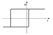
図3は、記録層12の理想的な電流−磁化曲線を表すグラフ図である。すなわち、同図の横軸は、記録層12に供給されるスピン偏極電流を表し、縦軸は、記録層の磁化Mを表す。同図から分かるように、VSMなどで測定した通常の強磁性体のMHカーブと同様の振舞いを示す。つまり、スピン偏極電流Iがある閾値を超えると、磁化Mが生ずる。
【0028】
一方、この電流閾値は、外部磁界に依存する。つまり、図3に例示した電流−磁化曲線は、外部磁界により横軸方向にシフトする。
【0029】
図4は、外部磁界Hを印加した状態での記録層12の電流−磁化曲線を例示するグラフ図である。すなわち、同図の横軸は、記録層12に供給されるスピン偏極電流を表し、縦軸は、記録層の磁化Mを表す。
【0030】
同図から分かるように、記録層12に磁化Mを生ずるためのスピン偏極電流の閾値は、外部磁界Hによってコントロールすることも可能である。
【0031】
以上説明したように、本発明においては、記録ヘッド16からの磁界により、スピンコントロール層14におけるスピン偏極の方向が制御される。そして、プローブ15から供給された電子のスピンは、スピンコントロール層14を通過する際に、そのスピン偏極の方向に偏極され、磁気記録層12に供給されて、そのスピンの向きに応じた磁化Mを書き込む。この書き込み電流は、その後、電極層11に流出する。
【0032】
またこの際に、図4に関して前述したように、記録ヘッド16からの外部磁界によって、記録層12のスピン偏極電流の書き込み閾値を制御することも可能である。
【0033】
本発明によれば、記録ヘッド16から印加する磁界は、特に微小範囲に制限する必要はなく、微小なプローブ15の先端から供給される局所的な電流により、磁気記録層12の極めて微小な範囲のみに書き込みを行うことができる。つまり、従来と比較して、飛躍的に記録密度を高めた超高密度磁気記録が可能となる。
【0034】
また一方、このように記録した情報の読み出しは、磁気抵抗効果を利用して行うことができる。すなわち、記録層12とスピンコントロール層14との間の抵抗を測定する。記録層12の磁化方向とスピンコントロール層14の磁化方向が平行の場合には抵抗が低く、両者の磁化が反平行の場合には抵抗が高い。
【0035】
スピンコントロール層14の磁化方向は、記録ヘッド16により所定の方向に制御することができるので、抵抗変化を検出することにより記録層12の磁化方向が分かる。
【0036】
ここで、読み出し時の電流は書き込み時の電流より小さくなければならない。もし、読み出し時の電流が書き込み時より大きいと記録層の磁化が反転し、情報を失ってしまうからである。
【0037】
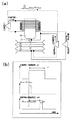
図5は本発明の実施の形態に係る磁気記録装置のシステム構成について説明する。図の様に3つのIC、あるいは同等の機能が有る複合ICでこの記録再生システムを駆動することができる。まず記録時には、記録用ICで記録回路1に駆動電流(Iw1)を発生させ、記録用コイルを励磁する。同時にタイミングパルスを発生させ記録用IC2を同期させる。記録用IC2ではタイミングパルスを基準にして、記録回路2にディレイタイム(t2)のタイミングで駆動電流Iw2を発生させる(図5(b))。こうすれば磁気記録媒体の高偏極スピンコントロール層14の磁化を所定の方向に磁化させた後に駆動電流Iw2で磁気記録層12の磁化を同方向に磁化することができる。この場合t2+t3とt1の両方の時間が最短ビット長をヘッドが横切る時間より小さいことが要求される。
【0038】
次に、再生時には、再生回路に再生用ICで一定のバイアス電流(Ib)を流し、媒体中の磁気抵抗効果で媒体に記録された磁化による抵抗変化、すなわち電圧変化を同じく再生用ICで読み取る。上述しているように、IbとIw2の関係は
Ib < Iw2 (1)
を満たす必要がある。以上は電流駆動による再生原理であるが、この磁気記録媒体10とプローブ15と記録ヘッド16を含む再生回路において、定電圧に保ったほうが良い場合もある。例えばプローブとヘッド境界の接触抵抗等は信頼性等により一定電圧に保つ方が有利である可能性がある。この場合は再生用ICで定電圧駆動でバイアス電流(Ib)を流し、同じく再生用ICで電流変化を読み取る方法が適している。以上のIw2、Ibの大きさ等は前述のような規定を用いるのが良い。
【0039】
以下、本発明において用いることができる磁気記録媒体10、プローブ15、磁気ヘッド16のそれぞれについて詳述する。
【0040】
まず、磁気記録媒体10について説明する。磁気記録媒体10は、図1に例示した基本的な構成要素の他にも、必要に応じて、磁気記録層12などの性能(結晶構造や配向特性など)を制御するための下地層(図示せず)を設けてもよい。また、必要に応じて、磁気記録層12やスピンコントロール層14の上に、カーボンやSiO2などからなる保護層(図示せず)を設けてもよい。
【0041】
また、記録媒体10は、面内方向に亘って複数の領域に分離された構造としてもよい。
【0042】
図6は、このように分離された記録媒体を表す模式図である。すなわち、同図に例示した記録媒体10Aは、電極層11の上に設けられた磁気記録層12、中間層13、スピンコントロール層14が、それぞれ分離領域18により複数の独立した部分に分割されている。分離領域18は、非磁性あるいは電気的絶縁性を有する材料により形成することができる。
【0043】
このように、分離領域18により、媒体を複数の部分に分割すると、記録ビットサイズを確実に規定することが可能となり、記録エリアの「はみ出し」、あるいはクロストーク(cross-talk)、クロスイレーズ(cross-erase)などの発生を抑制できる。
【0044】
また、このような分離領域18は、必ずしも記録層12、中間層13、スピンコントロール層14の全体を分割する必要はない。例えば、図7に例示した磁気記録媒体10Bの場合、磁気記録層12のみが分離領域18によって複数の独立した部分に分割されている。この場合にも、分離領域18は、非磁性あるいは電気的絶縁性を有する材料により形成することができ、記録ビットサイズを正確に規定できるという効果が得られる。同様に、分離領域18を中間層13のみ、あるいはスピンコントロール層14のみに設けても、電流狭窄作用などを利用した記録ビットサイズの規定が可能となる。
【0045】
さて、以上説明したいずれの磁気記録媒体においても、記録層12に用いられる磁性粒子の材料は、磁気異方性が大きいものが適している。この観点から、磁性金属材料として、コバルト(Co)、鉄(Fe)およびニッケル(Ni)からなる群より選択される磁性元素と、白金(Pt)、サマリウム(Sm)、クロム(Cr)、マンガン(Mn)、ビスマス(Bi)およびアルミニウム(Al)からなる群より選択される金属との合金を用いることが好ましい。
【0046】
特に、結晶磁気異方性の大きいコバルト(Co)基合金、特にCoPt、SmCo、CoCrをベースとしたものや、FePt、CoPtなどの規則合金がより好ましい。具体的には、Co−Cr、Co−Pt、Co−Cr−Ta、Co−Cr−Pt、Co−Cr−Ta−Pt、Fe50Pt50、Fe50Pd50、Co3Pt1などが挙げられる。
【0047】
また、磁性材料として、Tb−Fe、Tb−Fe−Co、Tb−Co、Gd−Tb−Fe−Co、Gd−Dy−Fe−Co、Nd−Fe−Co、Nd−Tb−Fe−Coなどの希土類(RE)−遷移金属(TM)合金、磁性層と貴金属層との多層膜(Co/Pt、Co/Pdなど)、PtMnSbなどの半金属、Coフェライト、Baフェライトなどの磁性酸化物などを用いることもできる。
【0048】
さらに、上述した磁性材料の磁気磁性を向上させるために、例えば銅(Cu)、クロム(Cr)、ニオブ(Nb)、バナジウム(V)、タンタル(Ta)、チタン(Ti)、タングステン(W)、ハフニウム(Hf)、インジウム(In)、シリコン(Si)、ボロン(B)など、またはこれらの元素と、酸素(O)、窒素(N)、炭素(C)、水素(H)の中から選ばれる少なくとも1種の元素との化合物を添加してもよい。
【0049】
磁気異方性に関しては、従来のHDDで用いられてきた面内磁気異方性でも、光磁気記録で用いられてきた垂直磁気異方性でも、両者が混合されたものでも構わない。磁気異方性定数に関しては、熱揺らぎ限界を打破するために大きな磁気異方性定数を有する記録層を用いる。さらに、磁気ヘッドからの磁界に影響されない程度のHcを有する必要もある。
【0050】
磁気記録層12として、例えば、複数の磁性粒子と、これら磁性粒子の間を埋める非磁性体とを有し、磁性粒子が非磁性体中に分散された構造を用いても構わない。
【0051】
磁性粒子を非磁性体により分断する方法は、特に限定されない。例えば、磁性材料に非磁性元素を添加して成膜し、磁性粒子の粒間にクロム(Cr)、タンタル(Ta)、ボロン(B)、酸化物(SiO2など)、窒化物などの非磁性体を析出させる方法を用いてもよい。
【0052】
また、リソグラフィー技術を利用して非磁性体に微細な孔を形成し、その孔に磁性粒子を埋め込む方法を用いてもよい。あるいは、PS−PMMAなどのジブロックコポリマーを自己組織化させて一方のポリマーを除去し、他方のポリマーをマスクとして非磁性体に微細な孔を形成し、孔に磁性粒子を埋め込む方法を用いてもよい。また、粒子線照射によって加工する方法を用いてもよい。
【0053】
記録層12の厚さは特に制限されないが、高密度記録を可能とし、電流を流すことを考慮すると、100nm以上の厚い膜は好ましくない。ただし、記録層12の厚さを0.1nm以下にしようとすると、膜を形成するのが困難になる場合が多いので、用いる成膜技術にも応じて適宜決定する必要がある。
【0054】
必要に応じて設けられる下地層(図示せず)は、磁性体でも非磁性体でもよい。下地層の厚さは特に限定されないが、500nmよりも厚いと製造コストが増加するので好ましくない。
【0055】
非磁性の下地層は、記録層12の磁性体または非磁性体の結晶構造を制御する目的、または基板からの不純物の混入を防ぐ目的で設けられる。例えば、磁性体に対して要求される結晶配向の格子間隔に近い格子間隔を有する下地層を用いれば、磁性体の結晶配向を制御することができる。また、適切な表面エネルギーを有するアモルファス下地層を用いることにより、記録層12の磁性体または非磁性体の結晶性またはアモルファス性を制御することもできる。
【0056】
下地層の下にさらに別の機能を有する下地層を設けてもよい。この場合、2つの下地層で機能を分担できるので、所望の効果の制御が容易になる。たとえば、記録層の結晶粒を小さくする目的で、基板上に粒径の小さいシード層を設け、その上に記録層の結晶性を制御する下地層を設ける手法が知られている。基板からの不純物の混入を防ぐためには、下地層として格子間隔が小さいかまたは緻密な薄膜を用いることが好ましい。
【0057】
高偏極スピンコントロール層14は、プローブ15から供給される電流を、記録層12に記録すべき磁化Mの方向のスピン偏極電流に変換する役割を有する。磁化Mの方向、すなわちスピンコントロール層14のスピン偏極の方向は、磁気ヘッド16からの磁界によって制御することができる。したがって、スピンコントロール層14は、磁気ヘッド16からの磁界に素早く応答することができる軟磁性で構成されていることが望ましい。また、スピン偏極を確実に行うため、高偏極スピンコントロール層14は、スピン偏極度の高い材料により形成されることが望ましい。ここで、スピン偏極度Pは、フェルミエネルギーにおけるアップスピン電子とダウンスピン電子の状態密度の差であり、次式により表される。
P=(D(↓)−D(↑))/(D(↓)+D(↑)) (2)
ここで、D(↑)とD(↓)は、アップスピン電子とダウンスピン電子の状態密度をそれぞれ表す。
【0058】
このスピン偏極度Pの最も大きな材料としては、「ハーフメタル」と呼ばれる物質が知られており、そのスピン偏極度は1.0である。すなわち、図8のようにダウンスピン電子のみが、フェルミエネルギー付近で状態密度を有する。
【0059】
ハーフメタル性を示す材料として知られているのは、コバルト(Co)、鉄(Fe)およびニッケル(Ni)の少なくともいずれからなるペロブスカイト型構造強磁性酸化物、ルチル型構造強磁性酸化物、スピネル型強磁性酸化物、パイロクロア型強磁性酸化物、少なくともチタン(Ti)、バナジウム(V)、クロム(Cr)、マンガン(Mn)、鉄(Fe)、コバルト(Co)、ニッケル(Ni)から選ばれる材料を含む磁性半導体薄膜などで、これらの材料を高偏極スピンコントロール層14に用いることができる。その他に、鉄(Fe)、コバルト(Co)、ニッケル(Ni)の単体や、鉄(Fe)、コバルト(Co)、ニッケル(Ni)を少なくとも一つ含む合金も、有限のスピン偏極度Pを示すことから高偏極スピンコントロール層14に用いることができる。
【0060】
高偏極スピンコントロール層14の厚さは特に制限されないが、高密度記録を達成し、且つ電流を垂直方向に流すことを考慮すると、100nm以上の厚い膜は好ましくない。ただし、記録層の厚さを0.1nm以下にしようとすると膜を形成するのが容易でないので、成膜技術も勘案して適宜決定する必要がある。
【0061】
また、高偏極スピンコントロール層14に関しては、例えば、複数の磁性粒子と磁性粒子の間を埋める絶縁体とを有し、磁性粒子が絶縁体中に分散された構造を用いても構わない。このような構造にすると、膜面に対して垂直方向の電流が面内方向に拡散することを防ぐことができる。
【0062】
中間層13は、高偏極スピンコントロール層14の磁化と記録層12の磁化とが交換結合することを防ぐ目的で設けられる。交換結合の大きさは、その間の距離が離れると減衰することが知られている。この観点からすると、厚い方が好ましいが、スピン偏極電流により記録層12に記録を行うことを考えると、スピン偏極電流の偏極方向が保存されなければならないので、その材料の平均自由行程より短くならなければならない。
【0063】
例えば、中間層13を銅(Cu)で構成した場合、銅(Cu)の平均自由行程は10nm程度であり、交換結合は3nm以上にすれば無視できる範囲になるので、銅(Cu)を利用した中間層13の厚さとして、3nmから10nmの範囲内にあることが好ましい、ということになる。
【0064】
記録媒体に対して電流を流す手段としては、導体あるいは半導体からなるプローブ15から、例えば、電界放出により電子を照射してもよいし、プローブ15と磁気記録媒体10とを接触させて電流を流してもよい。この場合のプローブとしては、金属や半導体などからなる針状あるいは先端に突起を有するものを用いることができる。また例えば、「カーボンナノチューブ」などの微細な構造体を利用することもできる。
【0065】
または、磁気記録媒体10の上部に図示しない電極を設け、その電極から磁気記録媒体10に電流を流してもよい。すなわち、磁気記録媒体10に電流を流せさえすれば、電流を流す手段としては、当業者が適宜選択したものを採用できる。
【0066】
磁気記録媒体10に対して磁界を印加する手段は、通常のHDDで用いられているような浮上スライダーの端面に誘導コイルと磁極を含む磁気回路を有するものでもよいし、永久磁石を設置してもよいし、媒体に磁性層を追加して温度分布または光照射によって磁化分布を生じさせ瞬間的・局所的な磁界を発生させてもよいし、情報の記録を行う磁性層自身から発生する漏洩磁界を利用してもよい。
【0067】
永久磁石を設置する場合には、媒体10との距離を可変にするか、磁石を微細化するなどの工夫によって、高速・高密度の磁界印加ができるようになる。
【0068】
図9は、プローブ15の代わりに、記録媒体10の上部に電極層19を設けた具体例を表す模式図である。すなわち、同図に例示した磁気記録媒体10Cは、下部電極層11の上に、記録層12、中間層13、高偏極スピンコントロール層14が積層され、さらにその上に、上部電極層19が設けられた構造を有する。そして、この積層構造は、分離領域18により複数の領域に分割されている。この分割された領域のそれぞれが、記録ビットとして作用する。
【0069】
この記録媒体10Cを用いる場合、上部電極19から下部電極11へ電流を膜面に対して垂直に流す。従って、分割された上部電極19のそれぞれに任意に電流を与えることができれば、図1に例示したプローブ15は必ずしも必要ない。
【0070】
以下、実施例を参照しつつ、本発明の実施の形態についてさらに詳細に説明する。
【0071】
(第1の実施例)
図10は、本実施例において用いた構成を表す概念図である。
【0072】
すなわち、高偏極スピンコントロール層14としてルチル型構造を示す酸化クロム(CrO2)を、記録層12としてコバルト白金(CoPt)を、中間層13として銅(Cu)を、電極層11として金(Au)をそれぞれ用いて記録媒体を作製した。
【0073】
まず、シリコン(Si)基板Sの裏側に金(Au)電極層11を形成した。次に、シリコン基板Sの上にコバルト白金(CoPt)層12を形成し、その上に銅(Cu)を成長させた。さらに、その上に酸化クロム(CrO2)を形成した。コバルト白金(CoPt)の厚さは約20ナノメートル、銅(Cu)は5ナノメートル、酸化クロム(CrO2)は10ナノメートルとした。
【0074】
次に、シリコン(Si)短針の表面を金(Au)でコートしたものをプローブ15として用いた。プローブ15はコーン状で、先端の直径は約10ナノメートルであった。さらに、磁気ヘッド16として、外部から2kOeの磁界を印加できるようにした。
【0075】
図11は、本実施例において形成した記録媒体に対して、VSMによる磁化測定を行った結果を表すグラフ図である。すなわち、同図の横軸は磁界H、縦軸は磁化Mをそれぞれ表す。なお、これとは別に測定したMH特性曲線から、本実施例に用いたものと同様の酸化クロム(CrO2)、コバルト白金(CoPt)の単層のHcは、それぞれ500Oe、2500Oeであった。
【0076】
図11から分かるように、本実施例の磁気記録媒体は、明らに2段のループを示しており、500Oe、2500Oe付近で磁化Mの変化が見られる。つまり、酸化クロム(CrO2)とコバルト白金(CoPt)の層が磁気的に交換結合していないために、それぞれのHcがお互いに影響を及ぼさない特性曲線が得られていることが分かった。
【0077】
つまり、中間層13として膜厚が5ナノメートルの銅(Cu)の層を挿入することにより、酸化クロム(CrO2)からなるスピンコントロール層14と、コバルト白金(CoPt)からなる記録層12の間の交換結合が作用していないことが確認できた。またさらに、磁界Hの方向が媒体面に対して垂直方向(面直方向)であったことから、コバルト白金(CoPt)層12の容易軸方向が面直方向になっていることが同時に確認できた。
【0078】
次に、スピン偏極電流磁気記録の実験を行った。
【0079】
まず、酸化クロム(CrO2)層14とコバルト白金(CoPt)層12の磁化を上向きの方向に揃えておく。この記録媒体に対して、下向きの磁界を加えて酸化クロム(CrO2)層14のみの磁化を反転させる。この状態でプローブ15から電子線照射を行い、同時に記録媒体の抵抗を測定した。電子線照射を行う前は、酸化クロム(CrO2)層14とコバルト白金(CoPt)層の磁化は反平行に配置されているため、高抵抗の状態である。プローブ15に対して約10Vの印加電圧で1mAの放出電流を確認し、記録媒体の抵抗値は約60mΩ低下した。このことから、プローブ15からの電子線放出により、コバルト白金(CoPt)記録層12の磁化が反転し、酸化クロム(CrO2)スピンコントロール層14の磁化と平行になったため、その抵抗は低下したと考えられる。つまり、プローブ15からの電子線照射により、記録層12に対する記録が行われることが確認できた。
【0080】
(第2の実施例)
図12は、本実施例において用いた構成を表す模式図である。
【0081】
すなわち、まず、シリコン(Si)基板Sの裏側にオーミックコンタクトとなるように金(Au)電極層11を形成した。そして、シリコン基板Sの上に、記録層12として鉄白金(FePt)を5nm形成し、その上に中間層13として銅(Cu)を5nm、高偏極スピンコントロール層14としてコバルトを添加した酸化亜鉛(ZnO:Co)を20nm積層した。さらに、その上にマスクを用いて金(Au)電極19を形成し、膜面垂直方向に電流を流せるようにした。
【0082】
鉄白金(FePt)単膜では、約9kOeのHcを示し、面直方向が磁化容易軸であることを確認し、コバルト添加酸化亜鉛(ZnO:Co)では、軟磁気特性を示すこともVSMで確認した。
【0083】
本実施例の記録媒体の3層構造(FePt/Cu/ZnO:Co)の磁気特性をVSMを用いて測定したところ、図9に表したものと類似した2段ループを示し、記録層12と高偏極スピンコントロール層14で磁気的に交換結合していないことが確認された。
【0084】
この記録媒体に、前述した第1実施例と同じように外部から磁界を印加した。記録実験の開始前に、記録層12と高偏極スピンコントロール層14の磁化はいずれも上向きの状態とした。次に、下向きの外部磁界を印加して、高偏極スピンコントロール層14の磁化を下向きに反転させた。このとき、記録層12の磁化と高偏極スピンコントロール層14の磁化は反平行状態にあるため、高抵抗の状態にある。
【0085】
次に、この記録媒体に対して、電極19から膜面垂直方向に電流を流した。電流値を大きくしていくと、20mA付近で抵抗値の大幅なジャンプが見られ、抵抗値は減少した。つまり、記録層12の磁化と高偏極スピンコントロール層14の磁化が平行状態になり、巨大磁気抵抗効果により抵抗が減少した。このようにして、記録層12の磁化が電流により反転可能であることを確認できた。
【0086】
(第3の実施例)
図13は、本実施例において用いた構成を表す模式図である。
【0087】
すなわち、アルミニウム基板11の上に、厚さ約50nmの白金(Pt)下地層20、厚さ約5nmの鉄白金(FePt)記録層12、厚さ約5nmの銅(Cu)中間層13、厚さ約20nmの酸化ランタン・ストロンチウム・マンガン(La0.7Sr0.3MnO3)高偏極スピンコントロール層14を、順次スパッタ法にて積層した。なお、スパッタ成膜時には、基板11を300℃に加熱した。
【0088】
ここで、La0.7Sr0.3MnO3高偏極スピンコントロール層14は、ハーフメタリックな特性を示すことを予め確認した。
【0089】
次に、リソグラフィとエッチング、さらにリフトオフにより、直径約50nmの円柱状のクラスターを作製した。クラスター間は絶縁体18で埋めた。その後、厚さ約1nmのカーボン(C)保護層21を積層した。鉄白金(FePt)記録層12は、約3.5kOeの保磁力を持ち、垂直磁気異方性を示すことを、VSMを用いた測定より予め確認した。
【0090】
次に、通常の磁気記録ヘッド16を用い、それに隣接するようにシリコン(Si)を金(Au)でコートしたプローブヘッド15を作製した。コーン状の形状をし、先端の直径は約50nmであった。プローブ15の先端と記録媒体との距離は約100nmとし、このとき印加電圧約10Vで10mAの放出電流を確認した。磁気記録ヘッド16からは、約3kOeの磁界を印加できる。つまり、鉄白金(FePt)記録層12の保磁力(3.5kOe)は、磁気ヘッド16からの磁界(3kOe)を超えているため、記録ヘッド16からの磁界のみで磁気記録することは困難である。
【0091】
本実施例においては、磁気記録媒体の記録及び再生評価を以下の手順で行った。
【0092】
まず、本実施例の磁気記録媒体についてプローブ15から電子線を照射しないで従来法による磁気記録を試みた。すなわち、記録ヘッド16から磁界を印加したが、記録層12の磁化は反転しないことが確認できた。これは、記録層12の保磁力と記録ヘッド16の記録能力から判断して当然の結果である。
【0093】
次に、本実施例の磁気記録媒体について電子線を照射しながら記録を行った。このとき、磁気ヘッド16から磁界を印加しなかった。初期状態として、記録層12、高偏極スピンコントロール層14の磁化をいずれも上向きに向けておいた。そして、プローブ15に対する印加電圧を10Vまで変化させて、印加電圧と媒体の電気抵抗の値との関係を調べた。しかしながら、印加電圧10Vまで、電気抵抗の変化は見られなかった。つまり、電子線照射のみによる記録は行われなかった。
【0094】
次に、ヘッド16から磁界を印加しながら、電子線を照射し記録することを試みた。印加磁界は、約3kOeで、下向きの磁界を与えた。そして、電子線の印加電圧を約10Vまで変化させた。その結果、約7V付近で、記録媒体の抵抗値の大幅な減少が見られた。すなわち、記録層12の磁化が反転して下向きになり、高偏極スピンコントロール層14の磁化と平行になったために抵抗が減少した。
【0095】
さらに、プローブ15に対する印加電圧をゼロに戻した後、磁気ヘッド16からの印加磁界の向きを逆向きにし、電気抵抗の値を測定したところ、媒体の抵抗値は先ほどの値よりも上昇していた。つまり、ヘッド16からの印加磁界により高偏極スピンコントロール層14の磁化のみが上向きに反転し、記録層12の磁化と反平行の状態になったために媒体の抵抗が増加した。このことからも、前述した記録過程で記録層12のみの磁化が反転したことが確認できた。
【0096】
本実施例の結果から、通常では記録不可能な大きな磁気異方性エネルギー(保磁力)を持つ記録層12に対して、電子線照射によるスピン偏極電流で記録が可能となることが確認できた。
【0097】
(第4の実施例)
次に、本発明の第4の実施例として、本発明の磁気記録装置の具体例について説明する。すなわち、図1乃至図13に関して説明した本発明の磁気記録方法は、従来のHDDに類似した構成を有する磁気記録再生装置として実現することができる。
【0098】
図14は、このような磁気記録再生装置の概略構成を例示する要部斜視図である。すなわち、本発明の磁気記録再生装置150は、ロータリーアクチュエータを用いた形式の装置である。同図において、記録用媒体ディスク200は、スピンドル152に装着され、図示しない駆動装置制御部からの制御信号に応答する図示しないモータにより矢印Aの方向に回転する。本発明の磁気記録再生装置150は、複数の媒体ディスク200を備えたものとしてもよい。さらにまた、媒体ディスク200は、磁気記録再生装置に定常的に備えられた、いわゆる「固定式」のものであってもよく、あるいはまた、媒体ディスク200を必要に応じて磁気記録再生装置から脱着可能な、いわゆる「リムーバブル式」のものとしてもよい。
【0099】
そして、これら媒体ディスク200は、前述したように、記録層12と高偏極スピンコントロール層14とを有し、スピン偏極電流を記録層12に流すことにより、磁化反転させて記録することができる。また、図6乃至図7あるいは図9、図13などに例示したように、分離領域18により記録ビットが分割されているパターンド媒体としてもよい。
【0100】
これら媒体ディスク200に格納する情報の記録再生を行うヘッドスライダ153は、薄膜状のサスペンション154の先端に取り付けられている。ここで、ヘッドスライダ153は、前述したような本発明のプローブ15及び磁気ヘッド16をその先端付近に搭載している。
【0101】
媒体ディスク200が回転すると、ヘッドスライダ153の媒体対向面(ABS)は媒体ディスク200の表面から所定の浮上量をもって保持される。あるいはスライダが媒体ディスク200と接触するいわゆる「接触走行型」であってもよい。
【0102】
サスペンション154は、図示しない駆動コイルを保持するボビン部などを有するアクチュエータアーム155の一端に接続されている。アクチュエータアーム155の他端には、リニアモータの一種であるボイスコイルモータ156が設けられている。ボイスコイルモータ156は、アクチュエータアーム155のボビン部に巻き上げられた図示しない駆動コイルと、このコイルを挟み込むように対向して配置された永久磁石および対向ヨークからなる磁気回路とから構成される。
【0103】
アクチュエータアーム155は、スピンドル157の上下2箇所に設けられた図示しないボールベアリングによって保持され、ボイスコイルモータ156により回転摺動が自在にできるようになっている。
【0104】
図15は、アクチュエータアーム155から先の磁気ヘッドアセンブリをディスク側から眺めた拡大斜視図である。すなわち、磁気ヘッドアッセンブリ160は、例えば駆動コイルを保持するボビン部などを有するアクチュエータアーム155を有し、アクチュエータアーム155の一端にはサスペンション154が接続されている。
サスペンション154の先端には、図1乃至図13に関して前述したような本発明のプローブ15及び磁気ヘッド16を具備するヘッドスライダ153が取り付けられている。サスペンション154は信号の書き込みおよび読み取り用のリード線164を有し、このリード線164とヘッドスライダ153に組み込まれた磁気ヘッドの各電極とが電気的に接続されている。図中165は磁気ヘッドアッセンブリ160の電極パッドである。
【0105】
本発明によれば、図1乃至図13に関して前述したような本発明の磁気記録媒体200に対して、磁気ヘッド16と、プローブ15とを用いて書き込みを行うことにより、従来よりも飛躍的に高い記録密度で媒体ディスク200に磁気的に情報を記録することが可能となる。
【0106】
また、再生に際しても、スライダ153に組み込まれたプローブ15をディスク200に接触させてその抵抗を測定してもよく、あるいは、巨大磁気抵抗効果素子などの磁界検出素子をスライダ153に別途組み込んで、記録層12の磁化方向を検出してもよい。
【0107】
(第5の実施例)
次に、本発明の第5の実施例として、本発明の磁気記録装置のもうひとつの具体例について説明する。
【0108】
図16は、このような磁気記録再生装置の概略構成を例示する要部斜視図である。本具体例の磁気記録再生装置は、パターニングされた記録媒体に対して、複数のプローブによりアクセスが可能とされている。
【0109】
すなわち、記録媒体10は、分離領域18によりパターニングされて記録ビットBがマトリクス状に配列した構造を有する。それぞれの記録ビットBは、挿入図に例示した如く、電極層11、記録層12、中間層13、高偏極スピンコントロール層14を積層した構造を有する。
【0110】
本具体例においても、記録媒体10は、磁気記録再生装置に定常的に備えられた、いわゆる「固定式」のものであってもよく、あるいはまた、記録媒体10を必要に応じて磁気記録再生装置から脱着可能な、いわゆる「リムーバブル式」のものとしてもよい。
【0111】
そして、このような記録媒体10の上に、複数のプローブ型ヘッドHを有するマルチヘッド部が配置される。プローブ型ヘッドHは、媒体に電流を供給するプローブ15と、磁界を印加する磁気ヘッド16とが一体化された構造を有する。このような構造を有する複数のヘッドHは、媒体の記録ビットBの配列ピッチ、あるいはその整数倍のピッチで設けられている。また、図16においては、プローブ型ヘッドHが、x方向に一列に配列されたマルチヘッド部を例示したが、本発明はこれには限定されず、プローブ型ヘッドHが、x及びy方向にマトリクス状に設けられたマルチヘッド部としてもよい。
【0112】
このようなマルチヘッド部は、記録媒体10に対して相対的にx、y方向に平行移動し、所定の記録ビットにアクセス可能とされている。この際に、マルチヘッド部が移動してもよく、あるいは記録媒体10が移動してもよい。また、書き込みに際して、プローブ15の先端が記録媒体10に接触してもよく、あるいは離間した状態で電界放出あるいはトンネリングにより電流を媒体10に供給してもよい。
【0113】
本具体例によれば、このようにパターニングされた記録媒体に対してマルチヘッドによりアクセスすることにより、超高密度のパターニングされた記録媒体10に対して、高速に記録再生動作をすることができる。
【0114】
以上、具体例を参照しつつ、本発明の実施の形態について説明した。しかし、本発明は、これらの具体例に限定されるものではない。例えば、磁気記録媒体、プローブ、磁気ヘッドなど、本発明の磁気記録装置を構成する各要素については、当業者が公知の範囲から適宜選択することにより本発明を同様に実施し、同様の効果を得ることができる。
【0115】
例えば、高偏極スピンコントロール層14や磁気記録層12などの材料や膜厚などの関しては、当業者が公知の範囲から適宜選択したものも本発明の範囲に包含される。
【0116】
その他、本発明の実施の形態として上述した磁気記録装置及び磁気記録方法を基にして、当業者が適宜設計変更して実施しうるすべての磁気記録装置及び磁気記録方法も同様に本発明の範囲に属する。
【0117】
【発明の効果】
以上詳述したように、本発明よれば、スピンコントロール層によりスピン偏極させた電流によって記録層の磁化を書き込むことにより、熱揺らぎ限界を超える高密度記録が実現可能となる。
【0118】
その結果として、従来よりも飛躍的に高感度の磁気記録再生が可能な磁気記録装置を提供することが可能となり産業上のメリットは多大である。
【図面の簡単な説明】
【図1】本発明の実施の形態に係る磁気記録方法の原理を表す概念図である。
【図2】本発明の実施の形態に係る磁気記録方法の原理を表す概念図である。
【図3】記録層12の理想的な電流−磁化曲線を表すグラフ図である。
【図4】外部磁界Hを印加した状態での記録層12の電流−磁化曲線を例示するグラフ図である。
【図5】本発明の実施の形態に係る磁気記録方法のシステム構成図を表す概念図である。
【図6】面内方向に亘って複数の領域に分離された記録媒体を表す模式図である。
【図7】磁気記録層12のみが分離領域18によって複数の独立した部分に分割された媒体を表す模式図である。
【図8】ハーフメタルの概念図である。
【図9】プローブ15の代わりに、記録媒体10の上部に電極層19を設けた具体例を表す模式図である。
【図10】本発明の第1の実施例において用いた構成を表す概念図である。
【図11】本発明の第1の実施例において形成した記録媒体に対して、VSMによる磁化測定を行った結果を表すグラフ図である。
【図12】本発明の第2の実施例において用いた構成を表す模式図である。
【図13】本発明の第3の実施例において用いた構成を表す模式図である。
【図14】本発明の磁気記録再生装置の概略構成を例示する要部斜視図である。
【図15】アクチュエータアーム155から先の磁気ヘッドアセンブリをディスク側から眺めた拡大斜視図である。
【図16】本発明の磁気記録再生装置の概略構成を例示する要部斜視図である。
【符号の説明】
10、10A〜C 磁気記録媒体
11 下部電極層(基板)
12 磁気記録層
13 中間層
14 高偏極スピンコントロール層
15 プローブ
16 磁気ヘッド
18 分離領域
19 上部電極
20 下地層
21 保護層
150 磁気記録再生装置
152 スピンドル
153 ヘッドスライダ
154 サスペンション
155 アクチュエータアーム
156 ボイスコイルモータ
157 スピンドル
160 磁気ヘッドアッセンブリ
164 リード線
165 図中
200 媒体ディスク
200 記録用媒体ディスク[0001]
BACKGROUND OF THE INVENTION
The present invention relates to a magnetic recording layer and a magnetic recording method, and more particularly, to a magnetic recording apparatus and a magnetic recording method capable of performing ultrahigh density magnetic recording exceeding the thermal fluctuation limit of a recording medium.
[0002]
[Prior art]
2. Description of the Related Art Along with recent improvements in computer processing speed, magnetic storage devices such as HDDs (Hard Disk Drives) that perform information / data storage / reproduction functions are constantly required to have high speed and high density. However, it is said that there is a physical limit to increasing the density, and it has been questioned whether it can continue to meet this requirement.
[0003]
In the case of an HDD device, a magnetic recording medium on which information is recorded has a magnetic layer including an aggregate of fine magnetic particles. In order to perform high density recording, it is necessary to reduce the magnetic domain recorded in the magnetic layer. In order to be able to sort out small recording magnetic domains, it is necessary that the boundaries of the magnetic domains be smooth. To that end, it is necessary to make the magnetic particles contained in the magnetic layer minute. In addition, if magnetization reversal is chained to adjacent magnetic particles, it becomes a “disturbance” at the boundary of the magnetic domain. Therefore, in order to prevent exchange coupling interaction between the magnetic particles, the magnetic particles are magnetically separated by non-magnetic materials. It needs to be divided. In addition, from the viewpoint of magnetic interaction between the head and the medium, it is necessary to reduce the thickness of the magnetic layer in order to perform high-density recording.
[0004]
From the above requirements, it is necessary to further reduce the volume of the magnetization reversal unit in the magnetic layer (which becomes almost equal to the magnetic particles when the above requirements are satisfied). However, when the magnetization reversal unit is miniaturized, the magnetic anisotropy energy (magnetic anisotropy energy density Ku × volume Va of the magnetization reversal unit) of the unit becomes smaller than the thermal fluctuation energy, and the magnetic domain is no longer retained. Can not be. This is the thermal fluctuation phenomenon, which is the main cause of the physical limit of recording density (called “thermal fluctuation limit”).
[0005]
In order to prevent magnetization reversal due to thermal fluctuation, it is conceivable to increase the magnetic anisotropy energy density Ku. However, in the case of the HDD medium as described above, the coercive force Hcw at the time of recording, that is, when performing a magnetization reversal operation at a high speed, is substantially proportional to Ku. Therefore, if Ku is increased, the magnetic field that can be generated by the current recording head. Then, it becomes impossible to record.
[0006]
In order to prevent magnetization reversal due to thermal fluctuation, it is conceivable to increase the volume Va of the magnetization reversal unit. However, if Va is increased by increasing the size of the magnetic particles in the medium plane, high-density recording cannot be achieved. If Va is increased by increasing the thickness of the recording layer, the head magnetic field does not sufficiently reach the lower portion of the recording layer, so that magnetization reversal does not occur, and high density recording cannot be achieved.
[0007]
Furthermore, since it is difficult to produce a recording / reproducing head in a minute size, it has become difficult to achieve high-density recording.
[0008]
Due to the circumstances described above, in order to achieve ultra-high density recording, there are many problems in the recording method using the recording magnetic field from the magnetic recording head and the method of detecting the leakage magnetic field from the recording pattern by the reproducing head, which depends on the current etc. It has become necessary to develop new recording and playback methods.
[Problems to be solved by the invention]
The present invention has been made based on the recognition of such problems, and an object of the present invention is to provide a novel magnetic recording apparatus and magnetic recording method capable of realizing high-density recording exceeding the thermal fluctuation limit.
[Means for Solving the Problems]
In order to achieve the above object, according to one aspect of the present invention,
A magnetic field applying unit that applies a magnetic field to the first magnetic layer of the magnetic recording medium and directs the magnetization direction;
Current supply means for supplying an energization current to the second magnetic layer of the magnetic recording medium via the first magnetic layer;
With
By energizing the second magnetic layer by the current supply means, the magnetization of the second magnetic layer is reversed by the spin-polarized current generated in the first magnetic layer, thereby magnetically information. Provided is a magnetic recording apparatus that performs recording.
[0009]
According to another aspect of the present invention,
A magnetic recording medium having a first magnetic layer and a second magnetic layer;
A magnetic field applying unit that applies a magnetic field to the first magnetic layer and directs the magnetization direction;
Current supply means for supplying a current to the second magnetic layer through the first magnetic layer;
With
By energizing the second magnetic layer by the current supply means, the magnetization of the second magnetic layer is reversed by the spin-polarized current generated in the first magnetic layer, thereby magnetically information. Provided is a magnetic recording apparatus that performs recording.
[0010]
Here, the magnetic recording medium may further include a non-magnetic layer inserted between the first and second magnetic layers.
In addition, the nonmagnetic layer of the magnetic recording medium is Cu, and may have a thickness of 2 nm to 10 nm.
[0011]
Further, the magnetic recording medium may be formed by two-dimensionally arranging a plurality of recording unit regions having the first and second magnetic layers with a separation region interposed therebetween.
[0012]
The coercive force of the first magnetic layer can be smaller than the coercive force of the second magnetic layer.
[0013]
The current supply means may be a conductor or semiconductor probe needle adjacent to the magnetic field application unit.
[0014]
Further, the range in which the magnetization direction of the first magnetic layer is directed by the magnetic field applied from the magnetic field applying unit is such that the second magnetic body is energized by energization of the second magnetic layer by the current supply means. It can be wider than the range in which the magnetization direction of the layer is reversed.
[0015]
Further, a magnetic field is applied to the first magnetic layer by the magnetic field applying unit, the magnetization direction thereof is directed, and the magnetoresistive effect between the first and second magnetic layers is changed to the first and second magnetic layers. Information detected magnetically on the second magnetic layer can be read by detecting a change in detection current supplied to the magnetic layer.
In addition, the magnetic field applied to the magnetic recording medium by the magnetic field application unit may have a strength that does not substantially change the magnetization direction of the second magnetic layer.
Further, the magnetic field applying unit can generate an applied magnetic field simultaneously with or before energization of the second magnetic layer by the current supply means.
The energization current during information recording supplied to the magnetic recording medium can be larger than the energization current during information reproduction.
[0016]
According to another aspect of the present invention,
Applying a magnetic field to the first magnetic layer of the magnetic recording medium to direct its magnetization direction;
Energizing the second magnetic layer of the magnetic recording medium through the first magnetic layer;
There is provided a magnetic recording method characterized in that information is magnetically recorded by reversing the magnetization of the second magnetic layer by a spin-polarized current generated in the first magnetic layer.
According to yet another aspect of the present invention,
Applying a magnetic field to the partial region of the first magnetic layer of the magnetic recording medium to direct the magnetization direction of the partial region;
In the second magnetic layer of the magnetic recording medium, at least one of the plurality of recording unit regions corresponding to the partial region is energized through the partial region, and by the spin-polarized current generated in the partial region A magnetic recording method is provided, wherein at least one magnetization of the plurality of recording unit regions is reversed.
DETAILED DESCRIPTION OF THE INVENTION
The basic principle of the present invention is that the current supplied from the current supply means is changed to a spin-polarized current by passing it through a highly polarized spin control layer through a probe, and the magnetization of the recording layer is changed using the spin-polarized current. Record by reversing. The direction of magnetization to be recorded is controlled by the magnetic field from the magnetic head in the highly polarized spin control layer. At the time of reproduction, reproduction is performed using a giant magnetoresistance effect by the relative angle between the magnetization of the highly polarized spin control layer and the magnetization of the recording layer.
[0017]
Hereinafter, embodiments of the present invention will be described with reference to the drawings.
[0018]
1 and 2 are conceptual diagrams showing the principle of a magnetic recording method according to an embodiment of the present invention. That is, this figure is a cross-sectional view schematically showing the
[0019]
The
[0020]
On the
[0021]
In the magnetic recording apparatus of the present invention, information recording, that is, “writing” is performed in accordance with FIGS. 1 (a) to 2 (c). FIG. 1A shows an initial state, and all the magnetizations of the
[0022]
In FIG. 1B, a downward magnetic field is emitted from the
[0023]
Thereafter, in FIG. 1C, electrons are supplied from the
[0024]
Next, in FIG. 2A, the
[0025]
In FIG. 2B, in order to record upward, an upward magnetic field is applied from the
[0026]
That is, the highly polarized
[0027]
FIG. 3 is a graph showing an ideal current-magnetization curve of the
[0028]
On the other hand, this current threshold depends on the external magnetic field. That is, the current-magnetization curve illustrated in FIG. 3 is shifted in the horizontal axis direction by the external magnetic field.
[0029]
FIG. 4 is a graph illustrating a current-magnetization curve of the
[0030]
As can be seen from the figure, the threshold value of the spin-polarized current for generating the magnetization M in the
[0031]
As described above, in the present invention, the direction of spin polarization in the
[0032]
At this time, as described above with reference to FIG. 4, the write threshold value of the spin-polarized current of the
[0033]
According to the present invention, the magnetic field applied from the
[0034]
On the other hand, the information recorded in this way can be read using the magnetoresistive effect. That is, the resistance between the
[0035]
Since the magnetization direction of the
[0036]
Here, the current during reading must be smaller than the current during writing. This is because if the current at the time of reading is larger than that at the time of writing, the magnetization of the recording layer is reversed and information is lost.
[0037]
FIG. 5 illustrates a system configuration of the magnetic recording apparatus according to the embodiment of the present invention. As shown in the figure, this recording / reproducing system can be driven by three ICs or a composite IC having an equivalent function. First, at the time of recording, a driving current (Iw1) is generated in the recording circuit 1 by the recording IC to excite the recording coil. At the same time, a timing pulse is generated to synchronize the recording IC 2. The recording IC 2 causes the recording circuit 2 to generate the drive current Iw2 at the timing of the delay time (t2) with reference to the timing pulse (FIG. 5B). In this way, the magnetization of the
[0038]
Next, at the time of reproduction, a constant bias current (Ib) is supplied to the reproduction circuit by the reproduction IC, and the resistance change due to the magnetization recorded on the medium due to the magnetoresistance effect in the medium, that is, the voltage change is read by the reproduction IC. . As mentioned above, the relationship between Ib and Iw2 is
Ib <Iw2 (1)
It is necessary to satisfy. The above is the principle of current-driven reproduction, but there are cases where it is better to maintain a constant voltage in the reproduction circuit including the
[0039]
Hereinafter, each of the
[0040]
First, the
[0041]
The
[0042]
FIG. 6 is a schematic diagram showing the recording medium separated in this way. That is, in the
[0043]
As described above, when the medium is divided into a plurality of parts by the
[0044]
Further, such a
[0045]
In any of the magnetic recording media described above, the material of the magnetic particles used for the
[0046]
In particular, cobalt (Co) based alloys having a large magnetocrystalline anisotropy, particularly those based on CoPt, SmCo, and CoCr, and ordered alloys such as FePt and CoPt are more preferable. Specifically, Co-Cr, Co-Pt, Co-Cr-Ta, Co-Cr-Pt, Co-Cr-Ta-Pt, Fe50Pt50, Fe50Pd50, Co3Pt1, etc. are mentioned.
[0047]
Further, as magnetic materials, Tb-Fe, Tb-Fe-Co, Tb-Co, Gd-Tb-Fe-Co, Gd-Dy-Fe-Co, Nd-Fe-Co, Nd-Tb-Fe-Co, etc. Rare earth (RE) -transition metal (TM) alloy, multilayer film of magnetic layer and noble metal layer (Co / Pt, Co / Pd, etc.), semimetal such as PtMnSb, magnetic oxide such as Co ferrite, Ba ferrite, etc. Can also be used.
[0048]
Furthermore, in order to improve the magnetic magnetism of the magnetic material described above, for example, copper (Cu), chromium (Cr), niobium (Nb), vanadium (V), tantalum (Ta), titanium (Ti), tungsten (W) , Hafnium (Hf), indium (In), silicon (Si), boron (B), etc., or these elements and oxygen (O), nitrogen (N), carbon (C), or hydrogen (H) A compound with at least one selected element may be added.
[0049]
Regarding magnetic anisotropy, in-plane magnetic anisotropy used in conventional HDDs, perpendicular magnetic anisotropy used in magneto-optical recording, or a mixture of both may be used. As for the magnetic anisotropy constant, a recording layer having a large magnetic anisotropy constant is used in order to overcome the thermal fluctuation limit. Furthermore, it is necessary to have Hc that is not affected by the magnetic field from the magnetic head.
[0050]
As the
[0051]
The method for dividing the magnetic particles with the non-magnetic material is not particularly limited. For example, a nonmagnetic element is added to a magnetic material to form a film, and chromium (Cr), tantalum (Ta), boron (B), oxide (SiO 2 Etc.), and a method of depositing a non-magnetic material such as nitride may be used.
[0052]
Alternatively, a method may be used in which a fine hole is formed in a nonmagnetic material using a lithography technique and magnetic particles are embedded in the hole. Alternatively, by using a method in which a diblock copolymer such as PS-PMMA is self-assembled to remove one polymer, a fine hole is formed in a non-magnetic material using the other polymer as a mask, and magnetic particles are embedded in the hole. Also good. Moreover, you may use the method processed by particle beam irradiation.
[0053]
The thickness of the
[0054]
The underlayer (not shown) provided as necessary may be a magnetic material or a non-magnetic material. The thickness of the underlayer is not particularly limited, but if it is thicker than 500 nm, the production cost increases, which is not preferable.
[0055]
The nonmagnetic underlayer is provided for the purpose of controlling the magnetic material of the
[0056]
A base layer having another function may be provided below the base layer. In this case, since the functions can be shared by the two underlayers, the desired effect can be easily controlled. For example, for the purpose of reducing the crystal grains of the recording layer, a technique is known in which a seed layer having a small particle diameter is provided on a substrate and an underlayer for controlling the crystallinity of the recording layer is provided thereon. In order to prevent entry of impurities from the substrate, it is preferable to use a thin film having a small lattice spacing or a dense base layer.
[0057]
The high polarization
P = (D (↓) −D (↑)) / (D (↓) + D (↑)) (2)
Here, D (↑) and D (↓) represent the density of states of up-spin electrons and down-spin electrons, respectively.
[0058]
As a material having the largest spin polarization degree P, a substance called “half metal” is known, and the spin polarization degree is 1.0. That is, as shown in FIG. 8, only the down spin electrons have a density of states in the vicinity of Fermi energy.
[0059]
Known materials exhibiting half-metal properties are perovskite structure ferromagnetic oxides, rutile structure ferromagnetic oxides, spinels made of at least one of cobalt (Co), iron (Fe), and nickel (Ni). Type ferromagnetic oxide, pyrochlore type ferromagnetic oxide, at least selected from titanium (Ti), vanadium (V), chromium (Cr), manganese (Mn), iron (Fe), cobalt (Co), nickel (Ni) These materials can be used for the highly polarized
[0060]
The thickness of the highly polarized
[0061]
For the highly polarized
[0062]
The
[0063]
For example, when the
[0064]
As a means for supplying a current to the recording medium, for example, electrons may be emitted from the
[0065]
Alternatively, an electrode (not shown) may be provided on the top of the
[0066]
The means for applying a magnetic field to the
[0067]
When a permanent magnet is installed, a high-speed and high-density magnetic field can be applied by changing the distance from the medium 10 or by miniaturizing the magnet.
[0068]
FIG. 9 is a schematic diagram showing a specific example in which an
[0069]
When this
[0070]
Hereinafter, embodiments of the present invention will be described in more detail with reference to examples.
[0071]
(First embodiment)
FIG. 10 is a conceptual diagram showing the configuration used in this embodiment.
[0072]
That is, chromium oxide (CrO) showing a rutile structure as the highly polarized
[0073]
First, the gold (Au)
[0074]
Next, the surface of a silicon (Si) short needle coated with gold (Au) was used as the
[0075]
FIG. 11 is a graph showing the results of VSM magnetization measurement performed on the recording medium formed in this example. That is, the horizontal axis of the figure represents the magnetic field H, and the vertical axis represents the magnetization M. In addition, from the MH characteristic curve measured separately from this, Hc of the single layer of chromium oxide (CrO2) and cobalt platinum (CoPt) similar to those used in this example was 500 Oe and 2500 Oe, respectively.
[0076]
As can be seen from FIG. 11, the magnetic recording medium of this example clearly shows a two-stage loop, and a change in the magnetization M is observed in the vicinity of 500 Oe and 2500 Oe. That is, since the chromium oxide (CrO2) and cobalt platinum (CoPt) layers are not magnetically exchange-coupled, it has been found that characteristic curves are obtained in which each Hc does not affect each other.
[0077]
That is, by inserting a copper (Cu) layer having a film thickness of 5 nanometers as the
[0078]
Next, an experiment of spin-polarized current magnetic recording was performed.
[0079]
First, the magnetizations of the chromium oxide (CrO2)
[0080]
(Second embodiment)
FIG. 12 is a schematic diagram showing the configuration used in this example.
[0081]
That is, first, the gold (Au)
[0082]
The iron-platinum (FePt) single film shows about 9 kOe of Hc, confirming that the perpendicular direction is the easy axis of magnetization, and cobalt-doped zinc oxide (ZnO: Co) also shows soft magnetic properties. confirmed.
[0083]
When the magnetic properties of the three-layer structure (FePt / Cu / ZnO: Co) of the recording medium of this example were measured using VSM, a two-stage loop similar to that shown in FIG. It was confirmed that the highly polarized
[0084]
A magnetic field was applied to the recording medium from the outside in the same manner as in the first embodiment. Prior to the start of the recording experiment, the magnetizations of the
[0085]
Next, a current was passed from the
[0086]
(Third embodiment)
FIG. 13 is a schematic diagram showing the configuration used in this example.
[0087]
That is, on an
[0088]
Where La 0.7 Sr 0.3 MnO 3 It has been confirmed in advance that the highly polarized
[0089]
Next, cylindrical clusters having a diameter of about 50 nm were produced by lithography, etching, and lift-off. Between the clusters was filled with an
[0090]
Next, a
[0091]
In this example, the recording and reproduction evaluation of the magnetic recording medium was performed according to the following procedure.
[0092]
First, with respect to the magnetic recording medium of this embodiment, magnetic recording by a conventional method was attempted without irradiating the
[0093]
Next, recording was performed while irradiating the magnetic recording medium of this example with an electron beam. At this time, no magnetic field was applied from the
[0094]
Next, recording was performed by irradiating an electron beam while applying a magnetic field from the
[0095]
Further, after the applied voltage to the
[0096]
From the results of this example, it can be confirmed that recording can be performed with a spin-polarized current by electron beam irradiation on the
[0097]
(Fourth embodiment)
Next, a specific example of the magnetic recording apparatus of the present invention will be described as a fourth embodiment of the present invention. That is, the magnetic recording method of the present invention described with reference to FIGS. 1 to 13 can be realized as a magnetic recording / reproducing apparatus having a configuration similar to a conventional HDD.
[0098]
FIG. 14 is a main part perspective view illustrating a schematic configuration of such a magnetic recording / reproducing apparatus. That is, the magnetic recording / reproducing
[0099]
These
[0100]
A
[0101]
When the
[0102]
The
[0103]
The
[0104]
FIG. 15 is an enlarged perspective view of the magnetic head assembly ahead of the
A
[0105]
According to the present invention, writing is performed on the
[0106]
Further, at the time of reproduction, the
[0107]
(Fifth embodiment)
Next, as a fifth embodiment of the present invention, another specific example of the magnetic recording apparatus of the present invention will be described.
[0108]
FIG. 16 is a main part perspective view illustrating a schematic configuration of such a magnetic recording / reproducing apparatus. In the magnetic recording / reproducing apparatus of this example, the patterned recording medium can be accessed by a plurality of probes.
[0109]
That is, the
[0110]
Also in this specific example, the
[0111]
A multi-head unit having a plurality of probe heads H is arranged on such a
[0112]
Such a multi-head unit moves in parallel in the x and y directions relative to the
[0113]
According to this specific example, by accessing the recording medium patterned in this way with a multi-head, it is possible to perform a recording / reproducing operation at a high speed with respect to the ultra-high-density patterned
[0114]
The embodiments of the present invention have been described above with reference to specific examples. However, the present invention is not limited to these specific examples. For example, for each element constituting the magnetic recording apparatus of the present invention, such as a magnetic recording medium, a probe, and a magnetic head, the person skilled in the art implements the present invention in a similar manner by selecting appropriately from a well-known range, and the same effect Can be obtained.
[0115]
For example, regarding the materials and film thicknesses of the highly polarized
[0116]
In addition, all magnetic recording apparatuses and magnetic recording methods that can be implemented by those skilled in the art based on the above-described magnetic recording apparatus and magnetic recording method as embodiments of the present invention are also included in the scope of the present invention. Belonging to.
[0117]
【The invention's effect】
As described above in detail, according to the present invention, high-density recording exceeding the thermal fluctuation limit can be realized by writing the magnetization of the recording layer with the current spin-polarized by the spin control layer.
[0118]
As a result, it is possible to provide a magnetic recording apparatus capable of performing magnetic recording / reproduction with significantly higher sensitivity than before, and the industrial merit is great.
[Brief description of the drawings]
FIG. 1 is a conceptual diagram showing the principle of a magnetic recording method according to an embodiment of the present invention.
FIG. 2 is a conceptual diagram showing the principle of a magnetic recording method according to an embodiment of the present invention.
3 is a graph showing an ideal current-magnetization curve of the
FIG. 4 is a graph illustrating a current-magnetization curve of the
FIG. 5 is a conceptual diagram showing a system configuration diagram of a magnetic recording method according to an embodiment of the present invention.
FIG. 6 is a schematic diagram showing a recording medium separated into a plurality of regions over an in-plane direction.
7 is a schematic diagram showing a medium in which only the
FIG. 8 is a conceptual diagram of half metal.
FIG. 9 is a schematic view showing a specific example in which an
FIG. 10 is a conceptual diagram showing the configuration used in the first embodiment of the present invention.
FIG. 11 is a graph showing the results of magnetization measurement by VSM on the recording medium formed in the first example of the present invention.
FIG. 12 is a schematic diagram showing a configuration used in a second example of the present invention.
FIG. 13 is a schematic diagram showing a configuration used in a third example of the present invention.
FIG. 14 is a perspective view of relevant parts illustrating a schematic configuration of a magnetic recording / reproducing apparatus of the present invention.
15 is an enlarged perspective view of the magnetic head assembly ahead of the
FIG. 16 is a perspective view illustrating the schematic structure of the magnetic recording / reproducing apparatus according to the present invention.
[Explanation of symbols]
10, 10A-C Magnetic recording medium
11 Lower electrode layer (substrate)
12 Magnetic recording layer
13 Middle layer
14 Highly polarized spin control layer
15 Probe
16 Magnetic head
18 Separation area
19 Upper electrode
20 Underlayer
21 Protective layer
150 Magnetic recording / reproducing apparatus
152 spindle
153 Head slider
154 suspension
155 Actuator arm
156 Voice coil motor
157 spindle
160 Magnetic head assembly
164 Lead wire
165 in the figure
200 media disc
200 Recording media disc
Claims (14)
前記磁気記録媒体の第2の磁性体層への通電電流を前記第1の磁性体層を介して供給する電流供給手段と、
を備え、
前記電流供給手段による前記第2の磁性体層への通電により、前記第1の磁性体層において発生させたスピン偏極電流によって前記第2の磁性体層の磁化を反転させて磁気的に情報記録を行うことを特徴とする磁気記録装置。A magnetic field applying unit that applies a magnetic field to the first magnetic layer of the magnetic recording medium and directs the magnetization direction;
Current supply means for supplying an energization current to the second magnetic layer of the magnetic recording medium via the first magnetic layer;
With
By energizing the second magnetic layer by the current supply means, the magnetization of the second magnetic layer is reversed by the spin-polarized current generated in the first magnetic layer, thereby magnetically information. A magnetic recording apparatus that performs recording.
前記第1の磁性体層に磁界を印加し、その磁化方向を方向付ける磁界印加部と、
前記第2の磁性体層への通電電流を前記第1の磁性体層を介して供給する電流供給手段と、
を備え、
前記電流供給手段による前記第2の磁性体層への通電により、前記第1の磁性体層において発生させたスピン偏極電流によって前記第2の磁性体層の磁化を反転させて磁気的に情報記録を行うことを特徴とする磁気記録装置。A magnetic recording medium having a first magnetic layer and a second magnetic layer;
A magnetic field applying unit that applies a magnetic field to the first magnetic layer and directs the magnetization direction;
Current supply means for supplying a current to the second magnetic layer through the first magnetic layer;
With
By energizing the second magnetic layer by the current supply means, the magnetization of the second magnetic layer is reversed by the spin-polarized current generated in the first magnetic layer, thereby magnetically information. A magnetic recording apparatus that performs recording.
前記電流供給手段による前記第2の磁性体層への通電により前記第2の磁性体層の磁化方向が反転される範囲よりも広いことを特徴とする請求項1〜7のいずれか1つに記載の磁気記録装置。The range in which the magnetization direction of the first magnetic layer is directed by the magnetic field applied from the magnetic field application unit is:
8. The method according to claim 1, wherein the magnetization direction of the second magnetic layer is wider than a range in which the magnetization direction of the second magnetic layer is reversed by energization of the second magnetic layer by the current supply unit. The magnetic recording device described.
前記磁気記録媒体の第2の磁性体層へ前記第1の磁性体層を介して通電し、
前記第1の磁性体層において発生させたスピン偏極電流によって前記第2の磁性体層の磁化を反転させて磁気的に情報記録を行うことを特徴とする磁気記録方法。Applying a magnetic field to the first magnetic layer of the magnetic recording medium to direct its magnetization direction;
Energizing the second magnetic layer of the magnetic recording medium through the first magnetic layer;
A magnetic recording method, wherein information recording is magnetically performed by reversing the magnetization of the second magnetic layer by a spin-polarized current generated in the first magnetic layer.
前記磁気記録媒体の第2の磁性体層において前記部分領域に対応する複数の記録単位領域の少なくとも一つに、前記部分領域を介して通電し、前記部分領域において発生させたスピン偏極電流により前記複数の記録単位領域の少なくとも一つの磁化を反転させることを特徴とする磁気記録方法。Applying a magnetic field to the partial region of the first magnetic layer of the magnetic recording medium to direct the magnetization direction of the partial region;
In the second magnetic layer of the magnetic recording medium, at least one of the plurality of recording unit areas corresponding to the partial area is energized through the partial area, and by the spin-polarized current generated in the partial area A magnetic recording method comprising reversing at least one magnetization of the plurality of recording unit regions.
Priority Applications (2)
| Application Number | Priority Date | Filing Date | Title |
|---|---|---|---|
| JP2002097446A JP3680035B2 (en) | 2002-03-29 | 2002-03-29 | Magnetic recording apparatus and magnetic recording method |
| US10/400,532 US6982845B2 (en) | 2002-03-29 | 2003-03-28 | Magnetic recording apparatus and magnetic recording method |
Applications Claiming Priority (1)
| Application Number | Priority Date | Filing Date | Title |
|---|---|---|---|
| JP2002097446A JP3680035B2 (en) | 2002-03-29 | 2002-03-29 | Magnetic recording apparatus and magnetic recording method |
Publications (2)
| Publication Number | Publication Date |
|---|---|
| JP2003296901A JP2003296901A (en) | 2003-10-17 |
| JP3680035B2 true JP3680035B2 (en) | 2005-08-10 |
Family
ID=29387692
Family Applications (1)
| Application Number | Title | Priority Date | Filing Date |
|---|---|---|---|
| JP2002097446A Expired - Fee Related JP3680035B2 (en) | 2002-03-29 | 2002-03-29 | Magnetic recording apparatus and magnetic recording method |
Country Status (2)
| Country | Link |
|---|---|
| US (1) | US6982845B2 (en) |
| JP (1) | JP3680035B2 (en) |
Families Citing this family (35)
| Publication number | Priority date | Publication date | Assignee | Title |
|---|---|---|---|---|
| JP4102280B2 (en) * | 2002-10-14 | 2008-06-18 | 三星電子株式会社 | Magnetic medium using spin-polarized electrons, information recording apparatus and recording method for magnetic medium |
| JP4113041B2 (en) * | 2003-05-14 | 2008-07-02 | 株式会社日立製作所 | Magnetization control method and information recording apparatus |
| US6885582B2 (en) * | 2003-06-12 | 2005-04-26 | Hewlett-Packard Development Company, L.P. | Magnetic memory storage device |
| JP4880894B2 (en) * | 2004-11-17 | 2012-02-22 | シャープ株式会社 | Semiconductor memory device structure and manufacturing method thereof |
| US7190539B1 (en) | 2004-12-29 | 2007-03-13 | Storage Technology Corporation | Magnetic recorder having carbon nanotubes embedded in anodic alumina for emitting electron beams to perform heat-assisted magnetic recording |
| KR100773546B1 (en) * | 2006-03-09 | 2007-11-07 | 삼성전자주식회사 | Magnetic recording media |
| JP4773254B2 (en) * | 2006-03-15 | 2011-09-14 | 太陽誘電株式会社 | High frequency magnetic thin film and high frequency electronic device |
| JP2007265503A (en) * | 2006-03-28 | 2007-10-11 | Toshiba Corp | Information recording and reproducing system |
| US8437104B2 (en) * | 2006-04-06 | 2013-05-07 | Sigma Pro Ltd. Llc | Read/write apparatus and method for a magnetic storage medium comprised of magnetic nanoparticles contained within nanotubes |
| US7687160B2 (en) | 2006-04-06 | 2010-03-30 | Winarski Tyson Y | Magnetic storage medium formed of carbon nanotube arrays |
| KR100803213B1 (en) * | 2006-06-27 | 2008-02-14 | 삼성전자주식회사 | Patterned magnetic recording media and manufacturing method thereof |
| JP2008277586A (en) * | 2007-04-27 | 2008-11-13 | Toshiba Corp | Magnetic element, magnetic recording head and magnetic recording apparatus |
| US8021769B2 (en) * | 2007-05-22 | 2011-09-20 | Hitachi Global Storage Technologies Netherlands B.V. | Patterned perpendicular magnetic recording medium with exchange coupled recording layer structure and magnetic recording system using the medium |
| KR20080108016A (en) * | 2007-06-07 | 2008-12-11 | 가부시끼가이샤 도시바 | Magnetic recording head and magnetic recording device |
| US8994587B2 (en) | 2010-05-14 | 2015-03-31 | Qualcomm Incorporated | Compressed sensing for navigation data |
| JP4358279B2 (en) | 2007-08-22 | 2009-11-04 | 株式会社東芝 | Magnetic recording head and magnetic recording apparatus |
| JP4919901B2 (en) * | 2007-09-04 | 2012-04-18 | 株式会社東芝 | Magnetic recording head and magnetic recording apparatus |
| JP4818234B2 (en) * | 2007-09-05 | 2011-11-16 | 株式会社東芝 | Magnetic recording / reproducing device |
| JP2009070439A (en) * | 2007-09-11 | 2009-04-02 | Toshiba Corp | Magnetic recording head and magnetic recording device |
| JP2009080878A (en) * | 2007-09-25 | 2009-04-16 | Toshiba Corp | Magnetic recording head and magnetic recording device |
| JP4929108B2 (en) * | 2007-09-25 | 2012-05-09 | 株式会社東芝 | Magnetic head and magnetic recording apparatus |
| JP2009080875A (en) * | 2007-09-25 | 2009-04-16 | Toshiba Corp | Magnetic head and magnetic recording system |
| US20090155627A1 (en) * | 2007-12-14 | 2009-06-18 | Hitachi Global Storage Technologies Netherlands B.V. | Discrete track media with a capped media structure having high moment and exchange |
| JP5361259B2 (en) | 2008-06-19 | 2013-12-04 | 株式会社東芝 | Spin torque oscillator, magnetic recording head, magnetic head assembly, and magnetic recording apparatus |
| JP2010003353A (en) | 2008-06-19 | 2010-01-07 | Toshiba Corp | Magnetic recording head, magnetic head assembly, and magnetic recorder |
| JP5377893B2 (en) * | 2008-06-19 | 2013-12-25 | 株式会社東芝 | Magnetic head assembly and magnetic recording / reproducing apparatus |
| JP2010040060A (en) * | 2008-07-31 | 2010-02-18 | Toshiba Corp | Magnetic head for high-frequency field assist recording and magnetic recording apparatus using the same |
| JP2010040126A (en) | 2008-08-06 | 2010-02-18 | Toshiba Corp | Magnetic recording head, magnetic head assembly, and magnetic recording device |
| JP5320009B2 (en) * | 2008-10-06 | 2013-10-23 | 株式会社東芝 | Spin torque oscillator, magnetic recording head, magnetic head assembly, and magnetic recording apparatus |
| JP5173750B2 (en) * | 2008-11-06 | 2013-04-03 | 株式会社東芝 | Spin torque oscillator, magnetic recording head, magnetic head assembly, and magnetic recording apparatus |
| JP5558698B2 (en) | 2008-11-28 | 2014-07-23 | 株式会社東芝 | Magnetic recording head, magnetic head assembly, magnetic recording apparatus, and magnetic recording method |
| JP5606482B2 (en) | 2012-03-26 | 2014-10-15 | 株式会社東芝 | Magnetic head, magnetic head assembly, magnetic recording / reproducing apparatus, and magnetic head manufacturing method |
| US9280996B2 (en) * | 2013-12-13 | 2016-03-08 | HGST Netherlands B.V. | All-optical magnetic recording system using FeMnPt media |
| JP6156518B2 (en) | 2014-01-23 | 2017-07-05 | 富士電機株式会社 | Perpendicular magnetic recording medium |
| EP3863030A1 (en) * | 2020-02-04 | 2021-08-11 | AT & S Austria Technologie & Systemtechnik Aktiengesellschaft | Substantially annular magnetic member with magnetic particles in non-magnetic matrix for component carrier |
Family Cites Families (5)
| Publication number | Priority date | Publication date | Assignee | Title |
|---|---|---|---|---|
| JPS5834474A (en) * | 1981-08-25 | 1983-02-28 | Fuji Xerox Co Ltd | Heat magnetic recording method |
| JP2743213B2 (en) * | 1990-07-25 | 1998-04-22 | キヤノン株式会社 | Apparatus and method for recording and / or reproducing |
| FR2817998B1 (en) * | 2000-12-07 | 2003-01-10 | Commissariat Energie Atomique | SPIN POLARIZATION MAGNETIC DEVICE WITH MAGNIFICATION ROTATION, MEMORY AND WRITING METHOD USING THE DEVICE |
| US6809900B2 (en) * | 2001-01-25 | 2004-10-26 | Seagate Technology Llc | Write head with magnetization controlled by spin-polarized electron current |
| JP2003091801A (en) | 2001-09-17 | 2003-03-28 | Toshiba Corp | Magnetic recording device and magnetic recording medium |
-
2002
- 2002-03-29 JP JP2002097446A patent/JP3680035B2/en not_active Expired - Fee Related
-
2003
- 2003-03-28 US US10/400,532 patent/US6982845B2/en not_active Expired - Lifetime
Also Published As
| Publication number | Publication date |
|---|---|
| US20030214742A1 (en) | 2003-11-20 |
| US6982845B2 (en) | 2006-01-03 |
| JP2003296901A (en) | 2003-10-17 |
Similar Documents
| Publication | Publication Date | Title |
|---|---|---|
| JP3680035B2 (en) | Magnetic recording apparatus and magnetic recording method | |
| JP3891540B2 (en) | Magnetoresistive memory, method for recording / reproducing information recorded in magnetoresistive memory, and MRAM | |
| Comstock | Review modern magnetic materials in data storage | |
| US5936810A (en) | Magnetoresistive effect head | |
| US8085499B2 (en) | Thin film perpendicular magnetic recording head, their fabrication process and magnetic disk drive using it | |
| US6804089B2 (en) | Yoke-type magnetic head and magnetic recording/reproducing device | |
| JP2009080904A (en) | Magnetic recording device | |
| US7719799B2 (en) | Magnetoresistive element, magnetic head and magnetic recording/reproducing apparatus | |
| JP2006073875A (en) | Magnetoresistance effect element, magnetic head, magnetic recording/reproducing device, and magnetic memory | |
| JP2007265503A (en) | Information recording and reproducing system | |
| JP2007012264A (en) | Magnetic head and magnetic recording apparatus | |
| KR100389598B1 (en) | Magnetoresistive sensor, magnetoresistive head, and magnetic recording/reproducing apparatus | |
| JP3989368B2 (en) | Magnetic head and magnetic recording apparatus | |
| JP2009158789A (en) | Galvanomagnetic device and magnetic sensor | |
| JP5714065B2 (en) | Magnetic recording device | |
| US6545847B2 (en) | Magnetoresistive effect head | |
| JP2005203535A (en) | Magnetic memory | |
| JP2004128026A (en) | Magnetoresistive effect element, magnetic head, magnetic recording device | |
| JP2821586B2 (en) | Thin film magnetic head | |
| JP5893184B2 (en) | Magnetic recording device |
Legal Events
| Date | Code | Title | Description |
|---|---|---|---|
| RD04 | Notification of resignation of power of attorney |
Free format text: JAPANESE INTERMEDIATE CODE: A7424 Effective date: 20040528 |
|
| A977 | Report on retrieval |
Free format text: JAPANESE INTERMEDIATE CODE: A971007 Effective date: 20041216 |
|
| A131 | Notification of reasons for refusal |
Free format text: JAPANESE INTERMEDIATE CODE: A131 Effective date: 20041221 |
|
| A521 | Request for written amendment filed |
Free format text: JAPANESE INTERMEDIATE CODE: A523 Effective date: 20050217 |
|
| TRDD | Decision of grant or rejection written | ||
| A01 | Written decision to grant a patent or to grant a registration (utility model) |
Free format text: JAPANESE INTERMEDIATE CODE: A01 Effective date: 20050506 |
|
| A61 | First payment of annual fees (during grant procedure) |
Free format text: JAPANESE INTERMEDIATE CODE: A61 Effective date: 20050516 |
|
| FPAY | Renewal fee payment (event date is renewal date of database) |
Free format text: PAYMENT UNTIL: 20090520 Year of fee payment: 4 |
|
| FPAY | Renewal fee payment (event date is renewal date of database) |
Free format text: PAYMENT UNTIL: 20090520 Year of fee payment: 4 |
|
| FPAY | Renewal fee payment (event date is renewal date of database) |
Free format text: PAYMENT UNTIL: 20100520 Year of fee payment: 5 |
|
| FPAY | Renewal fee payment (event date is renewal date of database) |
Free format text: PAYMENT UNTIL: 20110520 Year of fee payment: 6 |
|
| FPAY | Renewal fee payment (event date is renewal date of database) |
Free format text: PAYMENT UNTIL: 20110520 Year of fee payment: 6 |
|
| FPAY | Renewal fee payment (event date is renewal date of database) |
Free format text: PAYMENT UNTIL: 20120520 Year of fee payment: 7 |
|
| FPAY | Renewal fee payment (event date is renewal date of database) |
Free format text: PAYMENT UNTIL: 20120520 Year of fee payment: 7 |
|
| FPAY | Renewal fee payment (event date is renewal date of database) |
Free format text: PAYMENT UNTIL: 20130520 Year of fee payment: 8 |
|
| FPAY | Renewal fee payment (event date is renewal date of database) |
Free format text: PAYMENT UNTIL: 20130520 Year of fee payment: 8 |
|
| FPAY | Renewal fee payment (event date is renewal date of database) |
Free format text: PAYMENT UNTIL: 20140520 Year of fee payment: 9 |
|
| LAPS | Cancellation because of no payment of annual fees |