JP3673626B2 - Non-uniformity inspection method and apparatus for translucent material - Google Patents
Non-uniformity inspection method and apparatus for translucent material Download PDFInfo
- Publication number
- JP3673626B2 JP3673626B2 JP29243297A JP29243297A JP3673626B2 JP 3673626 B2 JP3673626 B2 JP 3673626B2 JP 29243297 A JP29243297 A JP 29243297A JP 29243297 A JP29243297 A JP 29243297A JP 3673626 B2 JP3673626 B2 JP 3673626B2
- Authority
- JP
- Japan
- Prior art keywords
- light
- substrate
- translucent substrate
- uniformity
- laser
- Prior art date
- Legal status (The legal status is an assumption and is not a legal conclusion. Google has not performed a legal analysis and makes no representation as to the accuracy of the status listed.)
- Expired - Lifetime
Links
Images


Landscapes
- Investigating Materials By The Use Of Optical Means Adapted For Particular Applications (AREA)
- Testing Of Optical Devices Or Fibers (AREA)
- Preparing Plates And Mask In Photomechanical Process (AREA)
Description
【0001】
【発明の属する技術分野】
本発明は、フォトマスク用透明基板であるガラスサブストレートなどの透光性物質の光学的な不均一性(欠陥)を検査する方法及びその装置に係り、特に、鏡面仕上げされた表面での全反射の性質を利用することによって、透光性物質の不均一性を高感度、高速度に検出できるようにした透光性物質の不均一性検査方法及びその装置に関するものである。
【0002】
【従来の技術】
半導体集積回路、フォトマスクなどの製造工程において、微細パターンの形成には、フォトリソグラフィー法が用いられている。例えば、半導体集積回路を製造する際には、高精度に研磨され鏡面仕上げされた透明基板上に遮光性膜(例えばクロム膜)によりパターンが形成されたフォトマスクを用いてパターンを転写している。このパターンの原盤とも言えるフォトマスクについての検査方法は、特開昭58―162038号公報に記載の面状態検査装置にみられるように、パターン面の微小な領域に光を集め、パターン面からの反射出力、透過出力を比較する方法が知られている。
【0003】
【発明が解決しようとする課題】
しかしながら、近年においてはパターンの高密度化に伴い、上記方法のようにパターン面の検査のみならず、高精度に研磨され鏡面仕上げされた透明基板そのものの微小な欠陥も欠陥検出の対象となっている。また、上述した方法では、パターン面の微小な領域に光を集めることから検査領域が広い範囲にわたっている場合には何らかの手段を用いて光を走査する必要があり、検査領域の面積に比例して検査時間がかかることと、欠陥の有無によってパターン自体及び透明基板に対する反射光・透過光の光量の差異ないし変化があまり大きくなく、透明基板の微細な欠陥検出への適用は困難であった。
【0004】
このような問題点を解決するために、本発明者は、透光性物質の光学的な不均一性を高感度、高速度に検出できる透光性物質の不均一性検査方法及びその装置を先に提案した(特願平9―192763)。
【0005】
この発明は、鏡面仕上げされた表面を有する透光性物質の不均一部分の有無を検査するものであって、前記透光性物質の光路が光学的に均一の場合には前記表面で全反射が起こるように透光性物質内に光を導入し、透光性物質内に導入され伝播する光の光路中に不均一部分が存在するときに、前記表面から光が漏出することから透光性物質の不均一性を検出することを特徴とするものである。
【0006】
しかし、一般にフォトマスク用透明基板であるガラスサブストレートは石英基板を用いるが、上記の検査方法及び検査装置を用いて、石英基板の不均一性を検査する場合、石英材料固有の微視的な密度のゆらぎに起因して散乱(レーリー散乱)が起こり、石英基板全体がぼんやりと光ってしまうことが確認された。微小な欠陥を検査するためには導入する光の波長を短くするのがよいが、レーリー散乱の強度は波長の4乗に反比例するため、波長を短くするにつれて、欠陥から漏出する光の強度とレーリー散乱による光の強度とのコントラストが低下してしまい、微細な欠陥の検出が困難となるという問題があった。
【0007】
そこで、本発明は、上記問題点を解決すべく、透光性物質に存在する微細な欠陥をもダイナミックに検出できる方法及びその装置、即ち、透光性物質の光学的な不均一性を高感度・高速度に検出できる実用性の高い透光性物質の不均一性検査方法及びその装置を提供することを目的とする。
【0008】
【課題を解決するための手段】
上記目的を達成するために、本発明に係る透光性基板の不均一性検査方法は、鏡面仕上げされた少なくとも一対の主表面及び少なくとも一対の端面を有する透光性基板の不均一性を検査する透光性基板の不均一性検査方法であって、
前記透光性基板は、この透光性基板にレーザー光を導入したときにその光路が光学的に均一の場合に、そのレーザー光を前記主表面及び端面の間で全反射を繰り返してほぼ透光性基板内に閉じ込められたような状態にできるものであり、
前記透光性基板に、この透光性基板の光路が光学的に均一の場合に、前記主表面及び端面の間で全反射を繰り返して透光性基板内にほぼ閉じ込められたような状態になるように少なくとも2つの異なる波長のレーザー光を導入し、
前記透光性基板に導入され伝播するレーザー光の光路中に不均一部分が存在するときに、前記導入したレーザー光の一部が前記透光性基板の主表面又は端面で全反射することなく、レーザー光に対応した波長の漏出光として外部に漏出することを利用し、前記漏出光を外部に配置した光検出手段でそれぞれ検出することによって前記透光性基板の不均一性を検査することを特徴とする。
【0009】
透光性物質に表面の傷等の不均一部分がなければ、透光性物質内に導入した光は表面で全反射して外部へは漏出しないが、不均一部分があると全反射条件が満足されず、透光性物質表面から光が漏れ出す。このように、物理的な臨界現象である幾何光学的な全反射を利用しているため、被検査物である透光性物質の不均一部分と均一部分における検査光に対する応答も臨界的であり、不均一性が劇的なコントラストで現れる。また、透光性物質表面の不均一性のみならず、内部の異物,不純物等による欠陥、あるいはガラスの脈理等に特徴的な、透過率は同じで屈折率だけが違う欠陥の検出に関しても、異物等のあるところや屈折率の違うところでは本来均一ならば通る光路(経路)を外れ、透光性物質外部へ漏れ出すことになるため検出可能になる。
【0010】
上記の原理に基づいて透光性物質の不均一性を検査するのであるが、透光性物質内に波長の異なる少なくとも2つの光を導入しているので、不均一性の検出がより容易となる。即ち、透光性物質内に導入された光は、透光性物質の微視的な密度のゆらぎに起因するレーリー散乱を受けるが、このレーリー散乱では、各波長の光が透光性物質内部の照射領域全体からそれぞれ一様に散乱されて外部に出てくるため、レーリー散乱光は、異なる波長の光が混合した色の光となる。これに対し、透光性物質の傷等の不均一による漏出光は、各波長の色の光が不均一部分よりそれぞれ漏出(異なる出射方向あるいは出射位置から漏出)する。このため、光の色(波長)の違いによって、レーリー散乱光と透光性物質の傷等の不均一による漏出光との区別が明確となり、傷等の不均一部分の検出が容易となる。例えば、導入する光として、波長543nmのグリーンレーザー光(緑)と、波長633nmのHe‐Neレーザー光(赤)とを用いた場合、レーリー散乱光は前記2つの光が混合した黄色となるが、不均一部分からの漏出光は、それぞれ導入したレーザー光である緑色や赤色の光となるので、検出し易くなる。
【0011】
上記不均一性検査方法において、透光性物質の不均一性を、透光性物質内に導入した光のうち何れか1つの波長の光が漏出することによって検出するようにすると、レーリー散乱光によるコントラストの低下を、光の色の違いによって簡易に防止できる。
【0012】
また、透光性物質の不均一性を、透光性物質内に導入した波長の異なる光が混合された光を除外して検出することによって、レーリー散乱光の影響を排除でき、不均一部分からの検出光がコントラスト良く現れるので、高性能・高精度の検査が実現できる。混合された光を除外するには、例えば、混合された光の波長域を吸収あるいは反射する(色)フィルターを利用して、混合された光をカットすればよい。
【0013】
更に、透光性物質内に導入する光のうち、ある一つの波長の光は透光性物質内全域に光が満たされる条件(例えば、ガラスサブストレートの場合、コーナーの面取り部からの光の導入)で導入し、別の波長の光は透光性物質の一表面から該表面内で光の入射位置を移動させて導入することにより、一つの波長の光のみ移動するだけで、透光性物質全域の不均一性を簡単且つ迅速に検出することが可能となるので好ましい。
【0014】
また、本発明にかかる透光性基板の不均一性検査装置は、鏡面仕上げされた少なくとも一対の主表面及び少なくとも一対の端面を有する透光性基板の不均一性を検査する透光性基板の不均一性検査装置であって、
前記透光性基板は、この透光性基板にレーザー光を導入したときにその光路が光学的に均一の場合に、そのレーザー光を前記主表面及び端面の間で全反射を繰り返してほぼ透光性基板内に閉じ込められたような状態にできるものであり、
前記透光性基板に、この透光性基板の光路が光学的に均一の場合に、前記主表面及び端面の間で全反射を繰り返して透光性基板内にほぼ閉じ込められたような状態になるように少なくとも2つの異なる波長のレーザー光を導入する照明手段と、
前記透光性基板に導入され伝播するレーザー光の光路中に不均一部分が存在するときに、前記導入したレーザー光の一部が前記透光性基板の主表面又は端面で全反射することなく、レーザー光に対応した波長の漏出光として外部に漏出することを利用し、前記漏出光を検出する光検出手段とを有することを特徴とする。
【0015】
上記不均一性検査装置において、照明手段のうち少なくとも1つの波長の光の入射位置を移動させる移動手段を設けると、透光性物質の全域を迅速に検査可能となる。
【0016】
【発明の実施の形態】
以下に本発明の実施の形態を図面を用いて説明する。図1は本発明の透光性物質の不均一性検査装置の一実施形態を示す概略構成図である。
【0017】
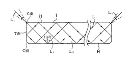
図1において、1は被検査対象である光学ガラス等のガラスからなる透明基板である。透明基板1は、図2に示すように、主表面(表面及び裏面)Hと端面(T面及び面取り部のC面からなる)とで区画され、いずれの面も鏡面研磨した後、洗浄処理されている。透明基板1は、その表面での全反射が阻害されず且つ漏出光の検査を容易とするために、フォルダーによってできるだけ接触部分を少なくして水平に保持される。図4は、透明基板1のフォルダーの一例を示すもので、フォルダー10は透明基板1を保持する矩形の枠体形状をなし、フォルダー10の底部内周側の四隅には、透明基板1の底面隅部を支持するための受け部11が形成されており、各受け部11には透明基板1と点状に接触して支持する球体12が設けられている。
【0018】
この透明基板1に対して、不均一性を検査するための光を透明基板1の側面側から導入するための照明手段が設けられている。照明手段は、異なる2つの波長λ1、λ2のレーザー光L1、L2をそれぞれ透明基板1内に導入するために、光源として2つのレーザー21、22を用いている。一方のレーザー21には、波長λ1のレーザー光L1を透明基板1の辺aのC面に所定の入射角度で入射させるためのミラー31、41が設けられている。ミラー31、41は透明基板1に対する入射角度を変動制御するための入射角度調整手段5を備えており、透明基板1内に導入されたレーザー光L1が全反射を起こす範囲内で入射角度を変動させて入射させることができるようになっている。
【0019】
また、もう一方のレーザー22に対しても同一構成のミラー32、42と入射角度調整手段5が設けられており、透明基板1の辺aと平行な辺cのC面に所定の入射角度で入射できるようになっている。レーザー21側の照明手段とレーザー22側の照明手段とは、透明基板1に対しそれぞれ異なる入射方向及び/又は入射位置から同一領域に光を導入するように、即ち、レーザー光L1、L2が、一辺b(ないしd)方向に基板1を切断したときの一平面状(薄板状)の同一領域に照射されるように、基板1に対して対称的に配置されている。また、レーザー光L1、L2を透明基板1全域に照射できるように、透明基板1はフォルダーとともに辺a(ないしc)の方向に、図示省略の移動手段によって移動できるようになっている。
【0020】
また、透明基板1の上方には、透明基板1から漏出するレーザー光を検出するための検出手段が設けられている。検出手段は、波長λ1と波長λ2の光が加法混色された波長の光を遮断するフィルター6と、CCDカメラ8と、フィルター6を透過した光をCCDカメラ8のCCD面上に結像する結像光学系7とを有する。結像光学系7には、フィルター6を透過した異なる波長λ1、λ2の光がCCDカメラ8のCCD面の違う位置に焦点を結ばせるように、色収差の強い単レンズ等を用いる。CCDカメラ8には、検出した画像を処理するためのコンピューター等からなる画像処理装置9が接続されている。
【0021】
次に、図1の検査装置を用いて行った具体的な検査方法を述べる。透明基板1として、152.4×152.4×6.35mmの大きさで、C面の幅が0.4mmのフォトマスク用ガラス基板(ガラスサブストレート)を検査した。このガラス基板のC面から導入したレーザー光が、図2に示すように、ガラス基板内で最初に当たる主表面Hへの入射角θi が臨界角θc よりも大きくなるようにレーザー光を入射した。ガラス基板の屈折率は1.47で、臨界角θc が約42.9°なので、入射角θiを45.0°とした。レーザー21として波長543.5nm(緑)のグリーンレーザー(パワー(出力)0.5mW、ビーム径0.7mm、ビームの広がり角1mrad)を使用し、レーザー22として波長632.8nm(赤)のHe‐Neレーザー(パワー(出力)5.0mW、ビーム径0.8mm、ビームの広がり角1mrad)を使用した。
【0022】
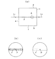
透明基板(ガラス基板)1内に入射したレーザー光L1、L2は、図2に示すように、基板1の主表面及び端面で全反射を繰り返し、基板1内にほぼ閉じ込められたような状態となり、基板1をその一辺b方向に切断したときの一断面状の同一領域に照射される。この際、入射角度調整手段5により、レーザー光の入射角θiを全反射を満足する45.0°〜44.0°の範囲で連続的に変化させているので、入射角度の変化に応じて基板1内を伝播する光線軌跡も少しずつずれることになり、基板1内の一断面状の全領域を覆いつくすように伝播する。研磨時の異物混入等によって基板1表面に傷等があると、その傷の部分から光が漏れ出る。この漏れ出た光が検出手段によって検出される。こうして、図3(a)に示すように基板1を上方からみて、1ライン状の照射領域Fの検査ができ、この工程をフォルダーとともに基板1をその一辺aに沿って移動させて行うことにより、基板1全域の不均一性の検査が行える。
【0023】
全反射による伝播を考えてみると、基板内の光は均一部分での極めてわずかな吸収を除けば、通過している間に、全く光が弱まる要素がなく、基板中を伝播し続ける。そのため、照射した光のほとんど全てが結果的に不均一部分へ集中することとなり、非常にはっきりしたコントラストで不均一部分が鋭敏に現れる。従って、微小な傷等を高感度で検出できる。
【0024】
基板1内に導入されたレーザー光L1(緑色)、L2(赤色)は、基板1を構成するガラスの微視的な密度のゆらぎに起因するレーリー散乱を受けるが、レーリー散乱光は、レーザー光L1、L2に対して基板1内の照射領域F全体からそれぞれ一様に発生する。このため、レーリー散乱による漏出光は、緑色の光と赤色の光とが混合した黄色の光となり、1ライン状の照射領域F全体がぼんやりと黄色に光る。一方、基板1の傷等の不均一による漏出光は、緑色と赤色の光が不均一部分Pよりそれぞれ漏出する。
【0025】
したがって、基板1の主表面を観察すると、図3(a)のA部を拡大した同図(b)に示すように、黄色くぼんやりと光った照射領域F内に、不均一部分Pがある場合、不均一部分及びその周辺が緑色や赤色の点状などに輝いてみえる。緑や赤に輝点状に輝く不均一部分Pの背景に黄色のレーリー散乱光があるため、コントラストは低下するが、漏出される光の色(波長)が違うので、レーリー散乱光を含む漏出光でも、単色(単一波長)の検査光を基板内に導入した場合に比べて、傷等の不均一部分の検出が容易となる。
【0026】
本実施形態では、基板1からの漏出光をそのまま観測するのではなく、黄色のレーリー散乱光を排除して、コントラストを高めている。即ち、基板1からの漏出光のうち、黄色のレーリー散乱光はフィルター6で遮断し、緑色と赤色の不均一性の検出光だけがフィルター6を透過するようにしている。このため、図3(c)に拡大して示すように、照射領域F全体から一様に散乱されていたレーリー散乱光がなくなり、不均一部分Pからの検出光だけが観測される。
【0027】
フィルター6を透過した緑色と赤色の検出光は、色収差の強いレンズ等を用いた結像光学系7により、CCDカメラ8のCCD面の異なる位置に結像される。CCDカメラ8に取り込まれた画像信号は、画像処理装置9に入力されデジタル変換された後、メモリに格納され、CPUで画像解析がなされる。一方、基板1の移動量(位置情報)がレーザー干渉計(図示せず)などから画像処理装置9に入力されており、CCDカメラ8の画像情報と基板1の位置情報とから、基板1に存在する傷等の不均一部分の位置、大きさ、種類等が求められる。
【0028】
上述の方法、装置によってガラス基板の不均一性を検査したところ、ガラス基板表面で傷と思われる箇所から光が漏出している(線状、点状などに輝いてみえる)ことを観察した。この輝いていた箇所を原子間力顕微鏡(AFM)で観察したところ、最小のもので幅0.04μm、深さ0.02μmの傷であることが確認された。このように、今までの光の反射出力、透過出力を比較することによって検査する散乱方式の検査方法、検査装置では、幅0.3μm程度の傷しか検出することができなかったが、本発明の検査方法、検査装置によって、幅0.05μm程度以下の傷までも検出することが可能となった。
【0029】
なお、上記の実施形態では、辺a、cから2つの波長の光をそれぞれ導入して辺b方向に光を照射したが、更に、例えば、基板1を90度回転して、辺b、dから2つの波長の光をそれぞれ導入して辺a方向に光を照射するするようにしてもよい。このようすると、直交する2方向(a方向とb方向)に光を照射して検査したことになるので、ガラスの傷等に特徴的な、特定の照射方向では強く光るため検出し易いが、照射方向によっては光の強度が弱いため検出し難いというような、光に対して方向性を有する欠陥の検出がより確実となる。
【0030】
また、ガラスの脈理等に特徴的な、透過率は同じで屈折率だけが違う欠陥の検出に関しても、屈折率の違うところで本来の軌道を外れ被検査物外部へ漏れ出すことになるため検出可能になる。しかし、集光した光の反射出力、透過出力という光量を検出する従来方法では、原理的にも捉えることは不可能である。
【0031】
上述した実施形態の検査方法を用いることによって、欠陥を持ったガラス基板を迅速・適切に排除することができ、ガラス基板の生産性を向上することができた。なお、表面上の傷などの欠陥を持ったガラス基板を再度精密に鏡面研磨、洗浄処理を行うことによって、仕様の範囲に入るフォトマスク用ガラス基板とすることができる。
【0032】
尚、上記実施形態では、波長の異なる2つのレーザー光L1、L2が、基板1をその一辺の方向に切断したときの断面状の同一領域内に照射されるようにしたが、図5に示すように、透明基板1内に導入する光のうち、ある一つの波長の光L1は、基板1全域に光が満たされるように、基板1の面取りされたコーナー部20から導入し、別の波長の光L2は基板1の一辺から光の入射位置を移動させて導入するようにしてもよい。こうすると、一つの波長の光L2のみ移動するだけで、基板1全域の不均一性を簡単且つ迅速に検出することが可能となるので好ましい。尚、この場合、コーナー部20から導入した光L1は基板全域に伝播するので、基板1の一辺から導入させた光L2に比べて、基板1内の照射強度が小さくなってしまうので、コーナー部20からの導入光L1の光量を、基板1の一辺から導入する光L2の光量より大きくしておくのがよい。
【0033】
また、波長の異なる2つのレーザー光がそれぞれ基板全域に満たされるように、2つの波長のレーザー光を基板のコーナー部からそれぞれ導入するようにしてもよい。更に、図6に示すように、波長の異なる2つの光L1、L2を、基板1の一端面側の面取りされた上下のC面からそれぞれ導入し、基板1の同一照射領域に2つの波長の光が照射されるようにしてもよい。
【0034】
また、上記実施形態では、基板1からの漏出光のうち、黄色のレーリー散乱光をフィルター6で遮断し、緑色と赤色の不均一性の検出光を観測しているが、例えば緑色の光だけを透過させるフィルターを用いて、緑色の検出光のみ観測するようにしてもよい。また、フィルター6を用いずに、CCDカメラ8で基板1からの光をカラー画像で検出し、画像処理装置9で黄色のレーリー散乱光を画像処理で取り除くようにしてもよい。
【0035】
また、上記実施形態では、波長の異なる2つのレーザー光を導入する例を挙げたが、例えば、0.1μm幅程度の傷を検査する必要がない場合は、波長633nm(赤)のHe‐Neレーザーをガラス基板に導入することによってレーリー散乱がほとんど発生しなくなるので、あえて波長の異なる2つの光を導入しなくてもよい。このように、検査で要求される仕様に応じて、適宜、レーザー光の波長や、レーザー光を導入する数、位置等を変えることによって効率の良い検査が可能である。
【0036】
また上記実施形態では、鏡面仕上げされた表面を有する透光性物質として、ガラス製の透明基板を挙げたが、ガラスに限らず、アクリル樹脂等の光学プラスチック、水晶等の光学結晶など、検査光が透過できる材質ならばどのようなものでもよい。
【0037】
また、透光性物質の形状は、矩形や円形等の基板に限らず、ブロック形状や曲面を有するものでもよい。更に、基板としては、フォトマスク(位相シフトマスク)用基板、液晶用ガラス基板、情報記録用ガラス基板(磁気ディスク、光ディスク等)など各種基板の検査に適用可能である。情報記録用ガラス基板は円盤状なので、実際に検査を行う場合には、研磨された外周あるいは内周端面(例えば面取り部)からレーザー光を入射させて行う。なお、基板両面の検査が必要な場合には、基板の上方及び下方にそれぞれ検出手段を設け、基板両面の検査を一度に行うようにしてもよい。
【0038】
また、上記実施形態では、レーザーとして、気体レーザー(He‐Neレーザー)を用いたが、これに限らず半導体レーザー等の可視域のレーザー、あるいは、透光性物質に対して吸収が少ないものであれば、紫外域のエキシマレーザーや、赤外域のNd‐YAGレーザー、CO2 レーザー等を検査用光源として使用することができる。特に、紫外域のレーザー(例えばエキシマレーザーやYAGレーザーの高調波等)を用いた場合、基板表面に付着している異物等を蒸発,蒸散等の作用により取り除くことが期待できるので好ましい。また、光閉じ込めのような多重反射ではなく、少数回の全反射でよい場合には、レーザー光でなく通常の光で検査することも可能である。
【0039】
また、上記実施形態では、波長の異なる2つのレーザー光を異なる位置、方向から導入する例を挙げたが、例えば、同時に複数の波長が得られるArレーザーのマルチラインを使えば、より装置の簡素化が図れる。
【0040】
また、上記実施形態では、基板に対する入射角度を変化させる角度調整手段をレーザーと基板との間にあるミラーに取り付けた例を挙げたが、基板に対するレーザー光の入射角度を変化させることができれば、どのようなような構成でもよく、レーザー自体に角度調整手段を設けたり、基板を支持するフォルダーに角度調整手段を設けてもよい。また、レーザー光の導光を、上記実施形態のようにミラーではなく、光ファイバーを用いて導光してもよい。この場合、光ファイバーからの出射光を平行光にするために、光ファイバー出射端部と基板との間にコリメートレンズを使用するのがよい。また、光ファイバーの出射端部をガイド等を用いて基板の各辺に沿って移動させたり、あるいは、光ファイバーの出射端部側に振動等を与えて入射角度を変動させたりしてもよい。
【0041】
また、上記実施形態では示さなかったが、実際に複数枚の透光性物質(ガラス基板等)を検査する場合には、透光性物質の表面状態を観察し、例えば鏡面仕上げされていない被検査物を取り除くためのTVカメラ、CCD撮像素子イメージセンサ等の装置を設けてもよい。
【0042】
更に、上記実施形態では、透明基板の面取り部の形状として、C面の幅が0.4mmのものを使用したが、基板内でより多く全反射を繰り返すことによって、基板全域にわたって不均一性を検査できるようにするためには、C面の幅は小さい程好ましく、0.4mm以下、より好ましくは0.2mm以下とするのがよい。しかし、極端に小さく(0.1mm未満に)すると、鏡面研磨時に基板端部に欠けが生じるので、好ましくない。
【0043】
【発明の効果】
以上詳述したように、本発明によれば、透光性物質内に波長の異なる少なくとも2つの光を導入しているので、レーリー散乱光は導入した異なる波長の光が混合した色の光となり、一方、透光性物質の傷等の不均一による漏出光は、導入した各波長の色の光となる。このため、光の色(波長)の違いによって、レーリー散乱光と透光性物質の傷等の不均一による漏出光との区別が明確となり、傷等の不均一部分の検出が容易となる。
【0044】
特に、透光性物質の不均一性を、透光性物質内に導入した波長の異なる光が混合された光を除外して検出することによって、レーリー散乱光の影響を排除でき、不均一部分からの検出光がコントラスト良く現れるので、高性能・高精度の検査が実現できる。
【図面の簡単な説明】
【図1】本発明に係る透光性物質の不均一性検査装置の一実施形態を示す概略構成図である。
【図2】図1の透明基板内における光の伝播の様子を拡大して示す側面図である。
【図3】図1の透明基板から出てくる光を観測したときの平面図である。
【図4】図1の透明基板を保持するフォルダーの一例を示す斜視図である。
【図5】透明基板に2つの異なる波長の光を導入する導入方法を示す斜視図である。
【図6】透明基板に2つの異なる波長の光を導入する導入方法を示す側面図である。
【符号の説明】
1 透明基板
21、22 レーザー
31、32、41、42 ミラー
5 入射角度調整手段
6 フィルター
7 結像光学系
8 CCDカメラ
9 画像処理装置
L1、L2 レーザー光[0001]
BACKGROUND OF THE INVENTION
The present invention relates to a method and an apparatus for inspecting optical non-uniformity (defect) of a light-transmitting substance such as a glass substrate which is a transparent substrate for a photomask, and more particularly to an entire surface on a mirror-finished surface. The present invention relates to a non-uniformity inspection method for a translucent substance and an apparatus thereof, which can detect nonuniformity of the translucent substance with high sensitivity and high speed by utilizing the property of reflection.
[0002]
[Prior art]
In the manufacturing process of a semiconductor integrated circuit, a photomask, and the like, a photolithography method is used for forming a fine pattern. For example, when a semiconductor integrated circuit is manufactured, a pattern is transferred using a photomask in which a pattern is formed with a light-shielding film (for example, a chromium film) on a transparent substrate that has been polished with high accuracy and is mirror-finished. . An inspection method for a photomask, which can be said to be a master of this pattern, collects light in a very small area of the pattern surface as seen in the surface state inspection apparatus described in Japanese Patent Application Laid-Open No. 58-162038. A method for comparing reflected output and transmitted output is known.
[0003]
[Problems to be solved by the invention]
However, in recent years, with the increase in pattern density, not only the inspection of the pattern surface as in the above method, but also the minute defect of the transparent substrate itself that has been polished and mirror finished with high accuracy becomes the object of defect detection. Yes. Further, in the above-described method, since light is collected in a small area of the pattern surface, it is necessary to scan the light using some means when the inspection area covers a wide range, which is proportional to the area of the inspection area. The difference or change in the amount of reflected / transmitted light with respect to the pattern itself and the transparent substrate is not so large depending on the inspection time and the presence / absence of a defect, and it is difficult to apply to the detection of minute defects on the transparent substrate.
[0004]
In order to solve such problems, the present inventor has developed a method and an apparatus for inspecting nonuniformity of a translucent substance that can detect optical nonuniformity of the translucent substance with high sensitivity and high speed. Proposed earlier (Japanese Patent Application No. 9-192863).
[0005]
The present invention inspects for the presence or absence of a non-uniform portion of a translucent material having a mirror-finished surface. When the optical path of the translucent material is optically uniform, the surface is totally reflected. When light is introduced into the light-transmitting material so that the light is introduced, and there is a non-uniform portion in the optical path of the light introduced and propagated in the light-transmitting material, the light is leaked from the surface. The present invention is characterized by detecting non-uniformity of a sexual substance.
[0006]
However, a glass substrate, which is a transparent substrate for a photomask, generally uses a quartz substrate. However, when inspecting the non-uniformity of the quartz substrate using the above-described inspection method and inspection apparatus, a microscopic characteristic inherent to the quartz material. It was confirmed that scattering (Rayleigh scattering) occurred due to density fluctuations, and the entire quartz substrate shined gently. In order to inspect minute defects, it is preferable to shorten the wavelength of the light to be introduced. However, since the intensity of Rayleigh scattering is inversely proportional to the fourth power of the wavelength, the intensity of light leaking from the defect increases as the wavelength is shortened. There is a problem that the contrast with the light intensity due to Rayleigh scattering is lowered, and it becomes difficult to detect fine defects.
[0007]
Therefore, in order to solve the above-described problems, the present invention provides a method and apparatus capable of dynamically detecting even a minute defect existing in a translucent material, that is, an optical non-uniformity of the translucent material. It is an object of the present invention to provide a highly practical method for inspecting non-uniformity of a translucent substance that can be detected with high sensitivity and high speed, and an apparatus therefor.
[0008]
[Means for Solving the Problems]
To achieve the above objective,A non-uniformity inspection method for a translucent substrate according to the present invention is a non-uniformity of a translucent substrate for inspecting non-uniformity of a translucent substrate having at least a pair of main surfaces and at least a pair of end surfaces that are mirror-finished. Sex testing method,
When the optical path is optically uniform when laser light is introduced into the translucent substrate, the translucent substrate repeats total reflection between the main surface and the end surface and substantially transmits the laser light. It can be in a state of being confined in the optical substrate,
When the optical path of the translucent substrate is optically uniform, the translucent substrate repeats total reflection between the main surface and the end surface and is almost confined in the translucent substrate. Introducing at least two different wavelengths of laser light,
When there is a non-uniform portion in the optical path of the laser beam introduced and propagated into the translucent substrate, a part of the introduced laser beam is not totally reflected at the main surface or end surface of the translucent substrate. Inspecting the non-uniformity of the translucent substrate by utilizing the leakage to the outside as leakage light having a wavelength corresponding to the laser light, and detecting the leakage light with a light detection means disposed outside. It is characterized by.
[0009]
If the translucent material does not have non-uniform parts such as scratches on the surface, the light introduced into the translucent substance is totally reflected on the surface and does not leak to the outside. Not satisfied, light leaks from the surface of the translucent material. As described above, since geometric optical total reflection, which is a physical critical phenomenon, is used, the response to the inspection light in the non-uniform part and the uniform part of the translucent material as the inspection object is also critical. , Non-uniformity appears with dramatic contrast. In addition to the non-uniformity of the surface of the translucent material, it is also related to the detection of defects due to internal foreign matter, impurities, etc., or defects with the same transmittance but different refractive index, which are characteristic of glass striae. In a place where there is a foreign substance or a place where the refractive index is different, if it is essentially uniform, the light path (path) that passes through will be removed, and it will leak out of the translucent substance, so that it can be detected.
[0010]
Based on the above principle, the non-uniformity of the translucent substance is inspected. However, since at least two lights having different wavelengths are introduced into the translucent substance, the non-uniformity can be detected more easily. Become. That is, the light introduced into the translucent material is subjected to Rayleigh scattering due to microscopic density fluctuations of the translucent material. In this Rayleigh scattering, light of each wavelength is transmitted inside the translucent material. Therefore, the Rayleigh scattered light is light of a color in which light of different wavelengths is mixed. On the other hand, light leaking due to non-uniformity such as scratches on the translucent substance leaks light of each wavelength color from the non-uniform part (leaks from different emission directions or emission positions). For this reason, the distinction between the Rayleigh scattered light and the leaked light due to non-uniformity such as scratches on the translucent substance becomes clear due to the difference in the color (wavelength) of light, and detection of non-uniform portions such as scratches becomes easy. For example, when a green laser beam (green) having a wavelength of 543 nm and a He—Ne laser beam (red) having a wavelength of 633 nm are used as the light to be introduced, the Rayleigh scattered light is a yellow color obtained by mixing the two lights. The leaked light from the non-uniform portion becomes green or red light, which is the introduced laser light, and is easy to detect.
[0011]
In the above non-uniformity inspection method, if the non-uniformity of the translucent material is detected by the leakage of light of any one wavelength among the light introduced into the translucent material, Rayleigh scattered light. It is possible to easily prevent a decrease in contrast due to the difference in light color.
[0012]
In addition, by detecting the inhomogeneity of the translucent material by excluding light mixed with light of different wavelengths introduced into the translucent material, the effect of Rayleigh scattered light can be eliminated, and the non-uniform part Because the detection light from the beam appears with good contrast, high-performance and high-precision inspection can be realized. In order to exclude the mixed light, for example, the mixed light may be cut using a (color) filter that absorbs or reflects the wavelength range of the mixed light.
[0013]
Furthermore, among the light introduced into the translucent material, the light having a certain wavelength has a condition that the entire region of the translucent material is filled with light (for example, in the case of a glass substrate, the light from the chamfered portion of the corner). Introduced in the introduction), light of another wavelength can be introduced by moving the incident position of light within the surface from one surface of the translucent substance, so that only the light of one wavelength moves. This is preferable because it is possible to easily and quickly detect the non-uniformity of the entire active substance.
[0014]
Further, the non-uniformity inspection apparatus for a translucent substrate according to the present invention is a translucent substrate inspecting non-uniformity of a translucent substrate having at least a pair of main surfaces and at least a pair of end surfaces that are mirror-finished. Non-uniformity inspection equipment,
When the optical path is optically uniform when laser light is introduced into the translucent substrate, the translucent substrate repeats total reflection between the main surface and the end surface and substantially transmits the laser light. It can be in a state of being confined in the optical substrate,
When the optical path of the translucent substrate is optically uniform, the translucent substrate repeats total reflection between the main surface and the end surface and is almost confined in the translucent substrate. Illuminating means for introducing laser light of at least two different wavelengths so that
When there is a non-uniform portion in the optical path of the laser beam introduced and propagated into the translucent substrate, a part of the introduced laser beam is not totally reflected at the main surface or end surface of the translucent substrate. And a light detecting means for detecting the leaked light by utilizing leaking to the outside as leaked light having a wavelength corresponding to the laser light.
[0015]
In the non-uniformity inspection apparatus, if the moving means for moving the incident position of the light having at least one wavelength among the illumination means is provided, the entire region of the translucent substance can be inspected quickly.
[0016]
DETAILED DESCRIPTION OF THE INVENTION
Embodiments of the present invention will be described below with reference to the drawings. FIG. 1 is a schematic configuration diagram showing an embodiment of a non-uniformity inspection apparatus for translucent substances according to the present invention.
[0017]
In FIG. 1, reference numeral 1 denotes a transparent substrate made of glass such as optical glass to be inspected. As shown in FIG. 2, the transparent substrate 1 is divided into a main surface (front surface and back surface) H and an end surface (consisting of a T surface and a C surface of a chamfered portion), and both surfaces are mirror-polished and then cleaned. Has been. The transparent substrate 1 is held horizontally with as few contacts as possible by a folder so that total reflection on the surface thereof is not hindered and leakage light can be easily inspected. FIG. 4 shows an example of the folder of the transparent substrate 1. The
[0018]
The transparent substrate 1 is provided with illumination means for introducing light for inspecting nonuniformity from the side surface side of the transparent substrate 1. The illumination means has two different wavelengths λ1, Λ2Laser light L1, L2In order to introduce each into the transparent substrate 1, two
[0019]
The
[0020]
A detection means for detecting laser light leaking from the transparent substrate 1 is provided above the transparent substrate 1. The detection means has a wavelength λ1And wavelength λ2A filter 6 that blocks light having a wavelength that is additively mixed, a CCD camera 8, and an imaging optical system 7 that forms an image of the light transmitted through the filter 6 on the CCD surface of the CCD camera 8. The imaging optical system 7 has different wavelengths λ transmitted through the filter 6.1, Λ2A single lens or the like having strong chromatic aberration is used so that the light is focused on a different position on the CCD surface of the CCD camera 8. Connected to the CCD camera 8 is an
[0021]
Next, a specific inspection method performed using the inspection apparatus of FIG. 1 will be described. As the transparent substrate 1, a glass substrate for a photomask (glass substrate) having a size of 152.4 × 152.4 × 6.35 mm and a C-plane width of 0.4 mm was inspected. As shown in FIG. 2, the laser light introduced from the C-plane of the glass substrate was incident so that the incident angle θi to the main surface H that first hits the glass substrate was larger than the critical angle θc. Since the refractive index of the glass substrate is 1.47 and the critical angle θc is about 42.9 °, the incident angle θi is set to 45.0 °.
[0022]
Laser light L entering the transparent substrate (glass substrate) 11,
[0023]
Considering the propagation by total reflection, the light within the substrate continues to propagate through the substrate without any element that attenuates the light while passing through, except for very little absorption at the uniform part. Therefore, almost all of the irradiated light is concentrated on the non-uniform portion as a result, and the non-uniform portion appears sharply with a very clear contrast. Therefore, minute scratches and the like can be detected with high sensitivity.
[0024]
Laser light L introduced into the substrate 11(Green), L2(Red) is subjected to Rayleigh scattering due to microscopic density fluctuations of the glass constituting the substrate 1, but the Rayleigh scattered light is a laser beam L1, L2On the other hand, they are uniformly generated from the entire irradiation region F in the substrate 1. For this reason, the leaked light due to Rayleigh scattering becomes yellow light in which green light and red light are mixed, and the entire irradiation area F in one line shape radiates yellow. On the other hand, as for leakage light due to non-uniformity such as scratches on the substrate 1, green and red light leak from the non-uniform part P, respectively.
[0025]
Accordingly, when the main surface of the substrate 1 is observed, as shown in FIG. 3B, which is an enlarged view of the portion A in FIG. The non-uniform portion and the periphery thereof shine like green or red dots. Since there is yellow Rayleigh scattered light in the background of the non-uniform part P that shines like green or red in the form of bright spots, the contrast decreases, but the color (wavelength) of the leaked light is different, so the leak that includes Rayleigh scattered light Even in the case of light, it is easier to detect a non-uniform portion such as a flaw as compared with a case where inspection light of a single color (single wavelength) is introduced into the substrate.
[0026]
In the present embodiment, the leakage light from the substrate 1 is not observed as it is, but the yellow Rayleigh scattered light is excluded to enhance the contrast. That is, of the leaked light from the substrate 1, yellow Rayleigh scattered light is blocked by the filter 6, and only green and red non-uniformity detection light is transmitted through the filter 6. For this reason, as shown in an enlarged view in FIG. 3C, the Rayleigh scattered light uniformly scattered from the entire irradiation region F disappears, and only the detection light from the non-uniform portion P is observed.
[0027]
The green and red detection lights transmitted through the filter 6 are imaged at different positions on the CCD surface of the CCD camera 8 by an imaging optical system 7 using a lens having strong chromatic aberration. The image signal captured by the CCD camera 8 is input to the
[0028]
When the non-uniformity of the glass substrate was inspected by the above-described method and apparatus, it was observed that light leaked out from a portion that seems to be a scratch on the surface of the glass substrate (it appears to shine in a linear shape, a dot shape, or the like). When this bright spot was observed with an atomic force microscope (AFM), it was confirmed that it was the smallest scratch having a width of 0.04 μm and a depth of 0.02 μm. As described above, in the scattering method and the inspection apparatus inspecting by comparing the reflected output and transmitted output of light so far, only a scratch having a width of about 0.3 μm could be detected. This inspection method and inspection apparatus can detect even scratches having a width of about 0.05 μm or less.
[0029]
In the above embodiment, light of two wavelengths is introduced from the sides a and c and irradiated in the direction of the side b. However, for example, the substrate 1 is rotated by 90 degrees, and the sides b and d are rotated. Alternatively, light having two wavelengths may be introduced to irradiate light in the direction of side a. In this way, since it was inspected by irradiating light in two orthogonal directions (a direction and b direction), it is easy to detect because it shines strongly in a specific irradiation direction characteristic of glass scratches, etc. Depending on the irradiation direction, the detection of a defect having directionality with respect to light, which is difficult to detect because the light intensity is weak, is more reliable.
[0030]
Also, detection of defects that are characteristic of glass striae, etc., with the same transmittance but only different refractive index, will be detected because they will escape from the original trajectory and leak out of the inspection object at different refractive indexes. It becomes possible. However, it is impossible in principle to grasp the conventional method of detecting the light amount of reflected output and transmitted output of condensed light.
[0031]
By using the inspection method of the above-described embodiment, a glass substrate having defects can be quickly and appropriately eliminated, and the productivity of the glass substrate can be improved. Note that a glass substrate for a photomask that falls within the specification range can be obtained by subjecting a glass substrate having defects such as scratches on the surface to mirror polishing and cleaning treatment with high precision again.
[0032]
In the above embodiment, two laser beams L having different wavelengths are used.1, L2However, as shown in FIG. 5, one of the lights introduced into the transparent substrate 1 is irradiated in the same region of the cross-sectional shape when the substrate 1 is cut in the direction of one side. Wavelength light L1Is introduced from the chamfered
[0033]
Alternatively, laser light of two wavelengths may be introduced from the corner portions of the substrate so that two laser beams having different wavelengths are filled in the entire substrate. Further, as shown in FIG. 6, two light beams L having different wavelengths are used.1, L2May be introduced from the upper and lower C planes chamfered on one end surface side of the substrate 1 so that the same irradiation region of the substrate 1 is irradiated with light of two wavelengths.
[0034]
Further, in the above embodiment, among the leaked light from the substrate 1, yellow Rayleigh scattered light is blocked by the filter 6 and green and red non-uniformity detection light is observed. For example, only green light is observed. Only the green detection light may be observed using a filter that transmits light. Alternatively, the light from the substrate 1 may be detected by a color image with the CCD camera 8 without using the filter 6, and the yellow Rayleigh scattered light may be removed by image processing with the
[0035]
In the above embodiment, an example in which two laser beams having different wavelengths are introduced has been described. For example, when it is not necessary to inspect a scratch having a width of about 0.1 μm, He—Ne having a wavelength of 633 nm (red). Since the Rayleigh scattering hardly occurs by introducing the laser into the glass substrate, it is not necessary to introduce two lights having different wavelengths. Thus, efficient inspection can be performed by appropriately changing the wavelength of the laser light, the number of laser light introduced, the position, and the like according to the specifications required for the inspection.
[0036]
Moreover, in the said embodiment, although the transparent substrate made from glass was mentioned as a translucent substance which has the surface by which the mirror surface was finished, inspection light, such as not only glass but optical plastics, such as an acrylic resin, optical crystals, such as a crystal, is mentioned. Any material can be used as long as it can pass through.
[0037]
Further, the shape of the translucent substance is not limited to a rectangular or circular substrate, but may be a block shape or a curved surface. Furthermore, the substrate can be applied to inspection of various substrates such as a photomask (phase shift mask) substrate, a liquid crystal glass substrate, and an information recording glass substrate (magnetic disk, optical disk, etc.). Since the information recording glass substrate is disk-shaped, when actually inspecting, laser light is incident from the polished outer peripheral or inner peripheral end face (for example, chamfered portion). If inspection of both sides of the substrate is necessary, detection means may be provided above and below the substrate, respectively, so that inspection on both sides of the substrate is performed at once.
[0038]
In the above embodiment, a gas laser (He-Ne laser) is used as the laser. However, the laser is not limited to this, and a laser in the visible region such as a semiconductor laser or a light-transmitting substance has little absorption. If so, an ultraviolet excimer laser, an infrared Nd-YAG laser, a CO2 laser, or the like can be used as an inspection light source. In particular, it is preferable to use an ultraviolet laser (for example, an excimer laser or a YAG laser harmonic) because foreign substances adhering to the substrate surface can be expected to be removed by an action such as evaporation or transpiration. In addition, when multiple reflections such as light confinement are sufficient instead of multiple reflections, it is possible to inspect with normal light instead of laser light.
[0039]
In the above embodiment, an example in which two laser beams having different wavelengths are introduced from different positions and directions has been described. For example, if an Ar laser multi-line capable of obtaining a plurality of wavelengths at the same time is used, the apparatus can be simplified. Can be achieved.
[0040]
In the above embodiment, an example in which the angle adjusting means for changing the incident angle with respect to the substrate is attached to the mirror between the laser and the substrate, but if the incident angle of the laser beam with respect to the substrate can be changed, Any configuration may be used, and the angle adjustment means may be provided in the laser itself, or the angle adjustment means may be provided in a folder that supports the substrate. Further, the laser light may be guided using an optical fiber instead of a mirror as in the above embodiment. In this case, a collimating lens is preferably used between the optical fiber output end and the substrate in order to make the output light from the optical fiber parallel light. Further, the exit end of the optical fiber may be moved along each side of the substrate using a guide or the like, or the incident angle may be changed by applying vibration or the like to the exit end of the optical fiber.
[0041]
Although not shown in the above embodiment, when actually inspecting a plurality of translucent materials (glass substrates, etc.), the surface state of the translucent material is observed, for example, a non-mirror-finished object. A device such as a TV camera or a CCD image sensor for removing an inspection object may be provided.
[0042]
Further, in the above embodiment, the shape of the chamfered portion of the transparent substrate is a C-plane having a width of 0.4 mm. However, non-uniformity is caused over the entire substrate by repeating total reflection more in the substrate. In order to be able to inspect, the width of the C surface is preferably as small as possible, 0.4 mm or less, more preferably 0.2 mm or less. However, if it is extremely small (less than 0.1 mm), chipping occurs at the edge of the substrate during mirror polishing, which is not preferable.
[0043]
【The invention's effect】
As described above in detail, according to the present invention, since at least two lights having different wavelengths are introduced into the translucent material, the Rayleigh scattered light becomes light of a color in which the introduced lights having different wavelengths are mixed. On the other hand, the leaked light due to non-uniformity such as scratches on the translucent material becomes light of the color of each introduced wavelength. For this reason, the distinction between the Rayleigh scattered light and the leaked light due to non-uniformity such as scratches on the translucent substance becomes clear due to the difference in the color (wavelength) of light, and detection of non-uniform portions such as scratches becomes easy.
[0044]
In particular, by detecting the non-uniformity of the translucent material by excluding light mixed with light of different wavelengths introduced into the translucent material, the effect of Rayleigh scattered light can be eliminated, and the non-uniform portion Because the detection light from the beam appears with good contrast, high-performance and high-precision inspection can be realized.
[Brief description of the drawings]
FIG. 1 is a schematic configuration diagram showing an embodiment of a non-uniformity inspection apparatus for translucent substances according to the present invention.
2 is an enlarged side view showing a state of light propagation in the transparent substrate of FIG. 1. FIG.
FIG. 3 is a plan view when light emitted from the transparent substrate of FIG. 1 is observed.
4 is a perspective view showing an example of a folder that holds the transparent substrate of FIG. 1. FIG.
FIG. 5 is a perspective view showing an introduction method for introducing light of two different wavelengths into a transparent substrate.
FIG. 6 is a side view showing an introduction method for introducing light of two different wavelengths into a transparent substrate.
[Explanation of symbols]
1 Transparent substrate
2122 laser
31324142 mirror
5 Incident angle adjustment means
6 Filter
7 Imaging optics
8 CCD camera
9 Image processing device
L1, L2 Laser light
Claims (6)
前記透光性基板は、この透光性基板にレーザー光を導入したときにその光路が光学的に均一の場合に、そのレーザー光を前記主表面及び端面の間で全反射を繰り返してほぼ透光性基板内に閉じ込められたような状態にできるものであり、
前記透光性基板に、この透光性基板の光路が光学的に均一の場合に、前記主表面及び端面の間で全反射を繰り返して透光性基板内にほぼ閉じ込められたような状態になるように少なくとも2つの異なる波長のレーザー光を導入し、
前記透光性基板に導入され伝播するレーザー光の光路中に不均一部分が存在するときに、前記導入したレーザー光の一部が前記透光性基板の主表面又は端面で全反射することなく、レーザー光に対応した波長の漏出光として外部に漏出することを利用し、前記漏出光を外部に配置した光検出手段で検出することによって前記透光性基板の不均一性を検査することを特徴とする透光性基板の不均一性検査方法。 A method for inspecting non-uniformity of a translucent substrate for inspecting non-uniformity of a translucent substrate having at least a pair of mirror-finished main surfaces and at least a pair of end surfaces ,
When the optical path is optically uniform when laser light is introduced into the translucent substrate, the translucent substrate repeats total reflection between the main surface and the end surface and substantially transmits the laser light. It can be in a state of being confined in the optical substrate,
When the optical path of the translucent substrate is optically uniform, the translucent substrate repeats total reflection between the main surface and the end surface and is almost confined in the translucent substrate. Introducing at least two different wavelengths of laser light,
When there is a non-uniform portion in the optical path of the laser beam introduced and propagated into the translucent substrate, a part of the introduced laser beam is not totally reflected at the main surface or end surface of the translucent substrate. Inspecting the non-uniformity of the translucent substrate by utilizing the leakage to the outside as leakage light having a wavelength corresponding to the laser light, and detecting the leakage light with a light detection means disposed outside. A method for inspecting non-uniformity of a translucent substrate.
前記透光性基板は、この透光性基板にレーザー光を導入したときにその光路が光学的に均一の場合に、そのレーザー光を前記主表面及び端面の間で全反射を繰り返してほぼ透光性基板内に閉じ込められたような状態にできるものであり、
前記透光性基板に、この透光性基板の光路が光学的に均一の場合に、前記主表面及び端面の間で全反射を繰り返して透光性基板内にほぼ閉じ込められたような状態になるように少なくとも2つの異なる波長のレーザー光を導入する照明手段と、
前記透光性基板に導入され伝播するレーザー光の光路中に不均一部分が存在するときに、前記導入したレーザー光の一部が前記透光性基板の主表面又は端面で全反射することなく、レーザー光に対応した波長の漏出光として外部に漏出することを利用し、前記漏出光を検出する光検出手段とを有することを特徴とする透光性基板の不均一性検査装置。 A non-uniformity inspection apparatus for a translucent substrate for inspecting non-uniformity of a translucent substrate having at least a pair of main surfaces and at least a pair of end surfaces mirror-finished ,
When the optical path is optically uniform when laser light is introduced into the translucent substrate, the translucent substrate repeats total reflection between the main surface and the end surface and substantially transmits the laser light. It can be in a state of being confined in the optical substrate,
When the optical path of the translucent substrate is optically uniform, the translucent substrate repeats total reflection between the main surface and the end surface and is almost confined in the translucent substrate. Illuminating means for introducing laser light of at least two different wavelengths so that
When there is a non-uniform portion in the optical path of the laser beam introduced and propagated into the translucent substrate, a part of the introduced laser beam is not totally reflected at the main surface or end surface of the translucent substrate. A non-uniformity inspection apparatus for a light-transmitting substrate, comprising: a light detecting means for detecting the leaked light by utilizing leaking to the outside as leaked light having a wavelength corresponding to the laser light.
Priority Applications (1)
| Application Number | Priority Date | Filing Date | Title |
|---|---|---|---|
| JP29243297A JP3673626B2 (en) | 1997-10-24 | 1997-10-24 | Non-uniformity inspection method and apparatus for translucent material |
Applications Claiming Priority (1)
| Application Number | Priority Date | Filing Date | Title |
|---|---|---|---|
| JP29243297A JP3673626B2 (en) | 1997-10-24 | 1997-10-24 | Non-uniformity inspection method and apparatus for translucent material |
Publications (2)
| Publication Number | Publication Date |
|---|---|
| JPH11132958A JPH11132958A (en) | 1999-05-21 |
| JP3673626B2 true JP3673626B2 (en) | 2005-07-20 |
Family
ID=17781723
Family Applications (1)
| Application Number | Title | Priority Date | Filing Date |
|---|---|---|---|
| JP29243297A Expired - Lifetime JP3673626B2 (en) | 1997-10-24 | 1997-10-24 | Non-uniformity inspection method and apparatus for translucent material |
Country Status (1)
| Country | Link |
|---|---|
| JP (1) | JP3673626B2 (en) |
Families Citing this family (14)
| Publication number | Priority date | Publication date | Assignee | Title |
|---|---|---|---|---|
| JP4721259B2 (en) * | 2004-08-30 | 2011-07-13 | Hoya株式会社 | Mask blank glass substrate manufacturing method, mask blank manufacturing method, and exposure mask manufacturing method |
| JP4520263B2 (en) * | 2004-09-16 | 2010-08-04 | Hoya株式会社 | Mask blank providing system, mask blank providing method, mask blank transparent substrate manufacturing method, mask blank manufacturing method, and mask manufacturing method |
| JP4979941B2 (en) | 2005-03-30 | 2012-07-18 | Hoya株式会社 | Manufacturing method of glass substrate for mask blanks, manufacturing method of mask blanks |
| CN1841189A (en) * | 2005-03-30 | 2006-10-04 | Hoya株式会社 | Mask blank glass substrate manufacturing method, mask blank manufacturing method, mask manufacturing method, mask blank glass substrate, mask blank, and mask |
| JP4688150B2 (en) * | 2005-08-03 | 2011-05-25 | Hoya株式会社 | Mask blank glass substrate manufacturing method, mask blank manufacturing method, exposure mask manufacturing method, and defect inspection apparatus |
| JP4761360B2 (en) * | 2005-10-25 | 2011-08-31 | Hoya株式会社 | Mask blank glass substrate manufacturing method, mask blank manufacturing method, exposure mask manufacturing method, and semiconductor device manufacturing method |
| JP5090379B2 (en) * | 2009-01-09 | 2012-12-05 | Hoya株式会社 | Manufacturing method of glass substrate for mask blank, manufacturing method of mask blank, and manufacturing method of photomask for exposure |
| JP5028437B2 (en) * | 2009-01-27 | 2012-09-19 | Hoya株式会社 | Manufacturing method of glass substrate for mask blank, manufacturing method of mask blank, and manufacturing method of photomask for exposure |
| KR101692087B1 (en) * | 2009-01-09 | 2017-01-02 | 호야 가부시키가이샤 | Method for manufacturing glass substrate for mask blank, method for manufacturing mask blank and method for manufacturing photomask for exposure |
| JP4520537B2 (en) * | 2010-03-08 | 2010-08-04 | Hoya株式会社 | Mask blank manufacturing method and mask manufacturing method |
| CN103105400B (en) * | 2013-01-29 | 2015-08-26 | 合肥知常光电科技有限公司 | The detection sorting technique of optical elements of large caliber surface imperfection |
| US10012598B2 (en) * | 2015-07-17 | 2018-07-03 | Emhart S.A. | Multi-wavelength laser check detection tool |
| US11340284B2 (en) * | 2019-07-23 | 2022-05-24 | Kla Corporation | Combined transmitted and reflected light imaging of internal cracks in semiconductor devices |
| RU2730929C1 (en) * | 2020-01-13 | 2020-08-26 | Российская Федерация, от имени которой выступает Государственная корпорация по атомной энергии "Росатом" (Госкорпорация "Росатом") | Method of estimating heterogeneity of structural materials and individual inhomogeneous areas by content of chemical elements |
-
1997
- 1997-10-24 JP JP29243297A patent/JP3673626B2/en not_active Expired - Lifetime
Also Published As
| Publication number | Publication date |
|---|---|
| JPH11132958A (en) | 1999-05-21 |
Similar Documents
| Publication | Publication Date | Title |
|---|---|---|
| KR100606460B1 (en) | Method of checking unevenness of light-transmitting substance, apparatus therefor, and method of sorting transparent substrates | |
| JP3422935B2 (en) | Inspection method and apparatus for non-uniformity of translucent substance and method for selecting transparent substrate | |
| JP3673626B2 (en) | Non-uniformity inspection method and apparatus for translucent material | |
| KR0127686B1 (en) | Method and apparatus for inspecting reticle for defects | |
| US10345246B2 (en) | Dark field wafer nano-defect inspection system with a singular beam | |
| JP3673649B2 (en) | Non-uniformity inspection method and inspection apparatus for translucent material | |
| KR102102020B1 (en) | Multi-spot illumination for improved detection sensitivity | |
| JP2001305072A (en) | Method and device for detecting defect in substrate | |
| JPH05264468A (en) | Method and apparatus for detecting internal | |
| JP3673632B2 (en) | Non-uniformity inspection method and apparatus for translucent material, and transparent substrate | |
| JP3673631B2 (en) | Non-uniformity inspection method and apparatus for translucent material | |
| JP3267551B2 (en) | Method for detecting defects in multilayer semiconductors etc. | |
| JP3186695B2 (en) | Device for detecting defects in semiconductors, etc. | |
| JPH06258238A (en) | Crystalline defect inspection method | |
| JPH11258172A (en) | Method and apparatus for inspection of heterogeneity of translucent substance | |
| KR0154559B1 (en) | Method of and apparatus for inspecting recticle for defects | |
| JPH10293103A (en) | Method and equipment for optical measurement and optical measuring equipment for patterned substrate | |
| KR102637273B1 (en) | Optical systems and methods for measuring parameters of patterned structures in microelectronic devices | |
| JP2005031689A (en) | Glass substrate for electronic device and photomask blank and photomask using the same | |
| JPH06138045A (en) | Defect inspecting device for glass substrate | |
| JP2001228096A (en) | Flaw inspection device | |
| JPH05322694A (en) | Lens inspection instrument | |
| JPH11183392A (en) | Heterogeneity inspecting method of light transmissive material and its device | |
| JPS63200043A (en) | Apparatus for detecting surface flaw of sheet like object to be inspected | |
| WO1998037407A1 (en) | Method and device for optically sensing properties object |
Legal Events
| Date | Code | Title | Description |
|---|---|---|---|
| A977 | Report on retrieval |
Free format text: JAPANESE INTERMEDIATE CODE: A971007 Effective date: 20040927 |
|
| A131 | Notification of reasons for refusal |
Free format text: JAPANESE INTERMEDIATE CODE: A131 Effective date: 20041026 |
|
| A521 | Written amendment |
Free format text: JAPANESE INTERMEDIATE CODE: A523 Effective date: 20041227 |
|
| TRDD | Decision of grant or rejection written | ||
| A01 | Written decision to grant a patent or to grant a registration (utility model) |
Free format text: JAPANESE INTERMEDIATE CODE: A01 Effective date: 20050419 |
|
| A61 | First payment of annual fees (during grant procedure) |
Free format text: JAPANESE INTERMEDIATE CODE: A61 Effective date: 20050425 |
|
| R150 | Certificate of patent or registration of utility model |
Free format text: JAPANESE INTERMEDIATE CODE: R150 |
|
| FPAY | Renewal fee payment (event date is renewal date of database) |
Free format text: PAYMENT UNTIL: 20090428 Year of fee payment: 4 |
|
| FPAY | Renewal fee payment (event date is renewal date of database) |
Free format text: PAYMENT UNTIL: 20090428 Year of fee payment: 4 |
|
| FPAY | Renewal fee payment (event date is renewal date of database) |
Free format text: PAYMENT UNTIL: 20100428 Year of fee payment: 5 |
|
| FPAY | Renewal fee payment (event date is renewal date of database) |
Free format text: PAYMENT UNTIL: 20110428 Year of fee payment: 6 |
|
| FPAY | Renewal fee payment (event date is renewal date of database) |
Free format text: PAYMENT UNTIL: 20120428 Year of fee payment: 7 |
|
| FPAY | Renewal fee payment (event date is renewal date of database) |
Free format text: PAYMENT UNTIL: 20130428 Year of fee payment: 8 |
|
| FPAY | Renewal fee payment (event date is renewal date of database) |
Free format text: PAYMENT UNTIL: 20130428 Year of fee payment: 8 |
|
| FPAY | Renewal fee payment (event date is renewal date of database) |
Free format text: PAYMENT UNTIL: 20140428 Year of fee payment: 9 |
|
| R250 | Receipt of annual fees |
Free format text: JAPANESE INTERMEDIATE CODE: R250 |
|
| R250 | Receipt of annual fees |
Free format text: JAPANESE INTERMEDIATE CODE: R250 |
|
| R250 | Receipt of annual fees |
Free format text: JAPANESE INTERMEDIATE CODE: R250 |
|
| R250 | Receipt of annual fees |
Free format text: JAPANESE INTERMEDIATE CODE: R250 |
|
| EXPY | Cancellation because of completion of term |