JP3661650B2 - Reference voltage generation circuit, display drive circuit, and display device - Google Patents
Reference voltage generation circuit, display drive circuit, and display device Download PDFInfo
- Publication number
- JP3661650B2 JP3661650B2 JP2002032677A JP2002032677A JP3661650B2 JP 3661650 B2 JP3661650 B2 JP 3661650B2 JP 2002032677 A JP2002032677 A JP 2002032677A JP 2002032677 A JP2002032677 A JP 2002032677A JP 3661650 B2 JP3661650 B2 JP 3661650B2
- Authority
- JP
- Japan
- Prior art keywords
- circuit
- reference voltage
- resistance
- voltage
- signal
- Prior art date
- Legal status (The legal status is an assumption and is not a legal conclusion. Google has not performed a legal analysis and makes no representation as to the accuracy of the status listed.)
- Expired - Fee Related
Links
Images


Classifications
-
- G—PHYSICS
- G09—EDUCATION; CRYPTOGRAPHY; DISPLAY; ADVERTISING; SEALS
- G09G—ARRANGEMENTS OR CIRCUITS FOR CONTROL OF INDICATING DEVICES USING STATIC MEANS TO PRESENT VARIABLE INFORMATION
- G09G3/00—Control arrangements or circuits, of interest only in connection with visual indicators other than cathode-ray tubes
- G09G3/20—Control arrangements or circuits, of interest only in connection with visual indicators other than cathode-ray tubes for presentation of an assembly of a number of characters, e.g. a page, by composing the assembly by combination of individual elements arranged in a matrix no fixed position being assigned to or needed to be assigned to the individual characters or partial characters
- G09G3/34—Control arrangements or circuits, of interest only in connection with visual indicators other than cathode-ray tubes for presentation of an assembly of a number of characters, e.g. a page, by composing the assembly by combination of individual elements arranged in a matrix no fixed position being assigned to or needed to be assigned to the individual characters or partial characters by control of light from an independent source
- G09G3/36—Control arrangements or circuits, of interest only in connection with visual indicators other than cathode-ray tubes for presentation of an assembly of a number of characters, e.g. a page, by composing the assembly by combination of individual elements arranged in a matrix no fixed position being assigned to or needed to be assigned to the individual characters or partial characters by control of light from an independent source using liquid crystals
-
- G—PHYSICS
- G09—EDUCATION; CRYPTOGRAPHY; DISPLAY; ADVERTISING; SEALS
- G09G—ARRANGEMENTS OR CIRCUITS FOR CONTROL OF INDICATING DEVICES USING STATIC MEANS TO PRESENT VARIABLE INFORMATION
- G09G3/00—Control arrangements or circuits, of interest only in connection with visual indicators other than cathode-ray tubes
- G09G3/20—Control arrangements or circuits, of interest only in connection with visual indicators other than cathode-ray tubes for presentation of an assembly of a number of characters, e.g. a page, by composing the assembly by combination of individual elements arranged in a matrix no fixed position being assigned to or needed to be assigned to the individual characters or partial characters
- G09G3/2007—Display of intermediate tones
- G09G3/2011—Display of intermediate tones by amplitude modulation
-
- G—PHYSICS
- G09—EDUCATION; CRYPTOGRAPHY; DISPLAY; ADVERTISING; SEALS
- G09G—ARRANGEMENTS OR CIRCUITS FOR CONTROL OF INDICATING DEVICES USING STATIC MEANS TO PRESENT VARIABLE INFORMATION
- G09G3/00—Control arrangements or circuits, of interest only in connection with visual indicators other than cathode-ray tubes
- G09G3/20—Control arrangements or circuits, of interest only in connection with visual indicators other than cathode-ray tubes for presentation of an assembly of a number of characters, e.g. a page, by composing the assembly by combination of individual elements arranged in a matrix no fixed position being assigned to or needed to be assigned to the individual characters or partial characters
- G09G3/34—Control arrangements or circuits, of interest only in connection with visual indicators other than cathode-ray tubes for presentation of an assembly of a number of characters, e.g. a page, by composing the assembly by combination of individual elements arranged in a matrix no fixed position being assigned to or needed to be assigned to the individual characters or partial characters by control of light from an independent source
- G09G3/36—Control arrangements or circuits, of interest only in connection with visual indicators other than cathode-ray tubes for presentation of an assembly of a number of characters, e.g. a page, by composing the assembly by combination of individual elements arranged in a matrix no fixed position being assigned to or needed to be assigned to the individual characters or partial characters by control of light from an independent source using liquid crystals
- G09G3/3611—Control of matrices with row and column drivers
- G09G3/3685—Details of drivers for data electrodes
- G09G3/3688—Details of drivers for data electrodes suitable for active matrices only
-
- G—PHYSICS
- G09—EDUCATION; CRYPTOGRAPHY; DISPLAY; ADVERTISING; SEALS
- G09G—ARRANGEMENTS OR CIRCUITS FOR CONTROL OF INDICATING DEVICES USING STATIC MEANS TO PRESENT VARIABLE INFORMATION
- G09G2300/00—Aspects of the constitution of display devices
- G09G2300/08—Active matrix structure, i.e. with use of active elements, inclusive of non-linear two terminal elements, in the pixels together with light emitting or modulating elements
- G09G2300/0809—Several active elements per pixel in active matrix panels
- G09G2300/0842—Several active elements per pixel in active matrix panels forming a memory circuit, e.g. a dynamic memory with one capacitor
- G09G2300/0861—Several active elements per pixel in active matrix panels forming a memory circuit, e.g. a dynamic memory with one capacitor with additional control of the display period without amending the charge stored in a pixel memory, e.g. by means of additional select electrodes
-
- G—PHYSICS
- G09—EDUCATION; CRYPTOGRAPHY; DISPLAY; ADVERTISING; SEALS
- G09G—ARRANGEMENTS OR CIRCUITS FOR CONTROL OF INDICATING DEVICES USING STATIC MEANS TO PRESENT VARIABLE INFORMATION
- G09G2310/00—Command of the display device
- G09G2310/02—Addressing, scanning or driving the display screen or processing steps related thereto
- G09G2310/0264—Details of driving circuits
- G09G2310/027—Details of drivers for data electrodes, the drivers handling digital grey scale data, e.g. use of D/A converters
-
- G—PHYSICS
- G09—EDUCATION; CRYPTOGRAPHY; DISPLAY; ADVERTISING; SEALS
- G09G—ARRANGEMENTS OR CIRCUITS FOR CONTROL OF INDICATING DEVICES USING STATIC MEANS TO PRESENT VARIABLE INFORMATION
- G09G2320/00—Control of display operating conditions
- G09G2320/02—Improving the quality of display appearance
- G09G2320/0271—Adjustment of the gradation levels within the range of the gradation scale, e.g. by redistribution or clipping
- G09G2320/0276—Adjustment of the gradation levels within the range of the gradation scale, e.g. by redistribution or clipping for the purpose of adaptation to the characteristics of a display device, i.e. gamma correction
-
- G—PHYSICS
- G09—EDUCATION; CRYPTOGRAPHY; DISPLAY; ADVERTISING; SEALS
- G09G—ARRANGEMENTS OR CIRCUITS FOR CONTROL OF INDICATING DEVICES USING STATIC MEANS TO PRESENT VARIABLE INFORMATION
- G09G3/00—Control arrangements or circuits, of interest only in connection with visual indicators other than cathode-ray tubes
- G09G3/20—Control arrangements or circuits, of interest only in connection with visual indicators other than cathode-ray tubes for presentation of an assembly of a number of characters, e.g. a page, by composing the assembly by combination of individual elements arranged in a matrix no fixed position being assigned to or needed to be assigned to the individual characters or partial characters
- G09G3/22—Control arrangements or circuits, of interest only in connection with visual indicators other than cathode-ray tubes for presentation of an assembly of a number of characters, e.g. a page, by composing the assembly by combination of individual elements arranged in a matrix no fixed position being assigned to or needed to be assigned to the individual characters or partial characters using controlled light sources
- G09G3/30—Control arrangements or circuits, of interest only in connection with visual indicators other than cathode-ray tubes for presentation of an assembly of a number of characters, e.g. a page, by composing the assembly by combination of individual elements arranged in a matrix no fixed position being assigned to or needed to be assigned to the individual characters or partial characters using controlled light sources using electroluminescent panels
- G09G3/32—Control arrangements or circuits, of interest only in connection with visual indicators other than cathode-ray tubes for presentation of an assembly of a number of characters, e.g. a page, by composing the assembly by combination of individual elements arranged in a matrix no fixed position being assigned to or needed to be assigned to the individual characters or partial characters using controlled light sources using electroluminescent panels semiconductive, e.g. using light-emitting diodes [LED]
- G09G3/3208—Control arrangements or circuits, of interest only in connection with visual indicators other than cathode-ray tubes for presentation of an assembly of a number of characters, e.g. a page, by composing the assembly by combination of individual elements arranged in a matrix no fixed position being assigned to or needed to be assigned to the individual characters or partial characters using controlled light sources using electroluminescent panels semiconductive, e.g. using light-emitting diodes [LED] organic, e.g. using organic light-emitting diodes [OLED]
- G09G3/3225—Control arrangements or circuits, of interest only in connection with visual indicators other than cathode-ray tubes for presentation of an assembly of a number of characters, e.g. a page, by composing the assembly by combination of individual elements arranged in a matrix no fixed position being assigned to or needed to be assigned to the individual characters or partial characters using controlled light sources using electroluminescent panels semiconductive, e.g. using light-emitting diodes [LED] organic, e.g. using organic light-emitting diodes [OLED] using an active matrix
- G09G3/3233—Control arrangements or circuits, of interest only in connection with visual indicators other than cathode-ray tubes for presentation of an assembly of a number of characters, e.g. a page, by composing the assembly by combination of individual elements arranged in a matrix no fixed position being assigned to or needed to be assigned to the individual characters or partial characters using controlled light sources using electroluminescent panels semiconductive, e.g. using light-emitting diodes [LED] organic, e.g. using organic light-emitting diodes [OLED] using an active matrix with pixel circuitry controlling the current through the light-emitting element
- G09G3/3241—Control arrangements or circuits, of interest only in connection with visual indicators other than cathode-ray tubes for presentation of an assembly of a number of characters, e.g. a page, by composing the assembly by combination of individual elements arranged in a matrix no fixed position being assigned to or needed to be assigned to the individual characters or partial characters using controlled light sources using electroluminescent panels semiconductive, e.g. using light-emitting diodes [LED] organic, e.g. using organic light-emitting diodes [OLED] using an active matrix with pixel circuitry controlling the current through the light-emitting element the current through the light-emitting element being set using a data current provided by the data driver, e.g. by using a two-transistor current mirror
- G09G3/325—Control arrangements or circuits, of interest only in connection with visual indicators other than cathode-ray tubes for presentation of an assembly of a number of characters, e.g. a page, by composing the assembly by combination of individual elements arranged in a matrix no fixed position being assigned to or needed to be assigned to the individual characters or partial characters using controlled light sources using electroluminescent panels semiconductive, e.g. using light-emitting diodes [LED] organic, e.g. using organic light-emitting diodes [OLED] using an active matrix with pixel circuitry controlling the current through the light-emitting element the current through the light-emitting element being set using a data current provided by the data driver, e.g. by using a two-transistor current mirror the data current flowing through the driving transistor during a setting phase, e.g. by using a switch for connecting the driving transistor to the data driver
Landscapes
- Engineering & Computer Science (AREA)
- Physics & Mathematics (AREA)
- Computer Hardware Design (AREA)
- General Physics & Mathematics (AREA)
- Theoretical Computer Science (AREA)
- Crystallography & Structural Chemistry (AREA)
- Chemical & Material Sciences (AREA)
- Liquid Crystal Display Device Control (AREA)
- Control Of Indicators Other Than Cathode Ray Tubes (AREA)
- Liquid Crystal (AREA)
- Control Of El Displays (AREA)
- Control Of Electrical Variables (AREA)
- Measurement Of Current Or Voltage (AREA)
Abstract
Description
【0001】
【発明の属する技術分野】
本発明は、基準電圧発生回路、表示駆動回路及び表示装置に関する。
【0002】
【背景技術及び発明が解決しようとする課題】
液晶装置等の電気光学装置に代表される表示装置は、小型化かつ高精細化が要求されている。中でも液晶装置は、低消費電力化が実現され、携帯型の電子機器に搭載されることが多い。例えば携帯電話機の表示部として搭載された場合、多階調化による色調豊富な画像表示が要求される。
【0003】
一般に、画像表示を行うための映像信号は、表示装置の表示特性に応じてガンマ補正が行われる。このガンマ補正は、ガンマ補正回路(広義には、基準電圧発生回路)により行われる。液晶装置を例にとれば、ガンマ補正回路は、階調表示を行うための階調データに基づいて、画素の透過率に応じた電圧を生成する。
【0004】
このようなガンマ補正回路は、表示装置を駆動する表示駆動回路に内蔵される。したがって、小型化が要求される電子機器に搭載される表示駆動回路は小規模であることが望ましい。そのため、ガンマ補正回路は、駆動する表示装置の表示特性に特化したガンマ補正を行うように調整されており、表示装置の種類に関わらず汎用的に用いられる表示駆動回路を提供することができなかった。
【0005】
本発明は、以上のような技術的課題に鑑みてなされたものであり、その目的とするところは、回路規模を増大させることなく、表示装置の種類に関わらず汎用的に用いられる基準電圧発生回路、表示駆動回路及び表示装置を提供することにある。
【0006】
【課題を解決するための手段】
上記課題を解決するために本発明は、階調データに基づいてガンマ補正された階調値を生成するための多値の基準電圧を発生する基準電圧発生回路であって、その両端の間の抵抗値が可変の可変抵抗回路を少なくとも1つ含み、多値の電圧を出力する第1のラダー抵抗回路と、抵抗値が固定の複数の抵抗回路が直列接続され、複数の電圧を出力する第2のラダー抵抗回路と、その両端の間の抵抗値が可変の可変抵抗回路を少なくとも1つ含み、多値の電圧を出力する第3のラダー抵抗回路とを含み、前記第1〜第3のラダー抵抗回路は、第1及び第2の電源電圧が供給される第1及び第2の電源線の間に直列に接続され、前記第1及び第3のラダー抵抗回路に含まれる可変抵抗回路は、所与のコマンド設定又は所与の可変制御信号に基づいて、抵抗値が可変制御されることを特徴とする。
【0007】
本発明において、第1及び第2の電源線の間に第1〜第3のラダー抵抗回路を直列に接続し、各ラダー抵抗回路から多値の基準電圧を出力させる。第1及び第3のラダー抵抗回路は、その両端の間の抵抗値が可変の可変抵抗回路を少なくとも1つ含み、第2のラダー抵抗回路は、抵抗値が固定の抵抗回路が直列接続されている。そして、第1及び第3のラダー抵抗回路は、例えばユーザからの所与のコマンドや所与の可変制御信号により可変制御されるが、第2のラダー抵抗回路はコマンドや可変制御信号によって抵抗値が変更されない構成となっている。
【0008】
ここで第1及び第3のラダー抵抗回路の可変制御を行うコマンドや可変制御信号は、同一のものであってもよいし、別個のものであってもよい。
【0009】
表示パネル、特に液晶パネルについては、液晶材等に依存して、最適な階調表現を行うための基準電圧が異なり、表示パネルの種類ごとにラダー抵抗の抵抗比を最適化する必要がある。しかしながら、中間調を表現する領域においては表示パネルの種類に関わらずほぼ一定である。したがって、本発明によれば、第1及び第3のラダー抵抗回路の抵抗値のみをコマンドや可変制御信号により可変制御を行って、表示パネルに応じた抵抗比を変更できるようにしたので、可変制御に伴う回路規模の増大を最低限に抑えつつ、表示パネルの種類に関わらず、最適な階調表現を行うためにガンマ補正された基準電圧を生成することができる。
【0010】
また本発明に係る基準電圧発生回路は、前記第1又は第3のラダー抵抗回路に含まれる可変抵抗回路は、スイッチ素子と抵抗素子とが直列接続された抵抗切替回路が並列接続されていてもよい。
【0011】
本発明によれば、スイッチ素子と抵抗素子とが直列接続された抵抗切替回路を用いて該抵抗切替回路を並列に接続することで、スイッチ素子の制御により多様な抵抗値を容易に実現させるようにしたので、簡素な構成で、上述のように汎用的な基準電圧発生回路を提供することができる。
【0012】
また本発明に係る基準電圧発生回路は、前記第1又は第3のラダー抵抗回路に含まれる可変抵抗回路は、前記抵抗切替回路と並列に接続された抵抗素子を含むことができる。
【0013】
本発明によれば、スイッチ素子を介さない抵抗回路を、抵抗切替回路と並列に接続するようにしたので、誤ったスイッチ制御によりオープンの状態を回避するための制御又は付加回路を簡素化することができる。
【0014】
また本発明に係る基準電圧発生回路は、前記第1又は第3のラダー抵抗回路に含まれる可変抵抗回路は、抵抗素子と該抵抗素子と並列に接続されたスイッチ素子とを含む抵抗切替回路が直列接続されていてもよい。
【0015】
本発明によれば、抵抗素子と該抵抗素子と並列に接続されたスイッチ素子とにより可変抵抗回路を構成し、スイッチ素子を制御して、多様な抵抗値を容易に実現させるようにしたので、簡素な構成で、上述のように汎用的な基準電圧発生回路を提供することができる。
【0016】
また本発明に係る基準電圧発生回路は、前記第1又は第3のラダー抵抗回路は、前記可変抵抗回路を少なくとも2つ有し、直列接続されていてもよい。
【0017】
本発明によれば、より高精度に抵抗比を制御することができ、汎用的な基準電圧発生回路を提供することができる。
【0018】
また本発明に係る基準電圧発生回路は、前記第1又は第3のラダー抵抗回路に含まれる可変抵抗回路は、第1〜第R(Rは2以上の整数)の基準電圧のうち第i(1≦i≦R、iは整数)の基準電圧を生成するための第i(iは正の整数)の分割ノードと第(i−1)の基準電圧を出力するための第(i−1)の分割ノードとの間に挿入された抵抗素子と、前記第iの分割ノードにその入力が接続されたボルテージフォロワ接続の第1の演算増幅回路と、第iの基準電圧の出力ノードと前記第1の演算増幅回路の出力との間に挿入された第1のスイッチ素子と、前記第iの基準電圧の出力ノードと前記第iの分割ノードとの間に挿入された第2のスイッチ素子とを含み、前記第1及び第2のスイッチ素子は、所与の駆動期間の前半期間において、前記第1のスイッチ素子がオン状態、前記第2のスイッチ素子がオフ状態に制御され、前記駆動期間の後半期間において、前記第1のスイッチ素子がオフ状態、前記第2のスイッチ素子がオン状態に制御され、前記第1の演算増幅回路は、前記後半期間において、その動作電流が制限又は停止されてもよい。
【0019】
本発明によれば、第1の演算増幅回路により、所与の基準電圧を迅速に駆動することができるようになるとともに、該第1の演算増幅回路の電流消費を最低限に抑えることができるので、駆動期間が短縮化された場合であっても低消費電力化を実現する基準電圧発生回路を提供することができる。
【0020】
本発明に係る基準電圧発生回路は、前記第1の演算増幅回路の出力と第(i+1)の基準電圧の出力ノードとの間に挿入された第2の演算増幅回路を含み、前記第2の演算増幅回路は、前記前半期間において、第iの基準電圧に所与のオフセット電圧を付加した電圧を出力し、前記後半期間において、その動作電流が制限又は停止されてもよい。
【0021】
本発明によれば、例えば中間調を表現するための基準電圧の立ち上げについても、第1の演算増幅回路により高速化し、かつ第2の演算増幅回路により付加されたオフセットにより高精度の駆動が可能となる。また、第2の演算増幅回路の電流消費を最低限に抑えることができる。
【0022】
また本発明に係る基準電圧発生回路は、前記第1〜第3のラダー抵抗回路を構成する第1〜第P(Pは正の整数)の抵抗回路のうち、第1の表示パネルを駆動する場合の第L(1≦L≦P、Lは整数)の抵抗回路の抵抗値を第1の抵抗値、第2の表示パネルを駆動する場合の第Lの抵抗回路の抵抗値を第2の抵抗値とした場合、前記第2のラダー抵抗回路は、前記第2の抵抗値に対する前記第1の抵抗値の比が2以下となる抵抗回路により構成されてもよい。
【0023】
本発明によれば、階調表現を損なうことなく、表示パネルの種類に依存しない基準電圧発生回路を提供することができる。
【0024】
また本発明に係る表示駆動回路は、上記いずれか記載の基準電圧発生回路と、前記基準電圧発生回路によって発生された多値の基準電圧から、階調データに基づいて電圧を選択する電圧選択回路と、前記電圧選択回路によって選択された電圧を用いて信号電極を駆動する信号電極駆動回路とを含むことができる。
【0025】
本発明によれば、汎用的なガンマ補正回路を含む表示駆動回路を提供することができ、低コスト化を図ることができる。
【0026】
また本発明に係る表示駆動回路は、前記可変制御信号が入力される外部入力端子を含むことができる。
【0027】
本発明によれば、ユーザ自身が表示パネルに応じて、容易に調整可能な表示駆動回路を提供することができる。
【0028】
また本発明係る表示装置は、複数の信号電極と、前記複数の信号電極と交差する複数の走査電極と、前記複数の信号電極と前記複数の走査電極とにより特定される画素と、前記複数の信号電極を駆動する上記記載の表示駆動回路と、前記複数の走査電極を駆動する走査電極駆動回路とを含むことができる。
【0029】
本発明によれば、表示パネルの種類に依存しない汎用的な表示駆動回路により、低コストに表示装置を提供することができる。
【0030】
また本発明に係る表示装置は、複数の信号電極と、前記複数の信号電極と交差する複数の走査電極と、前記複数の信号電極と前記複数の走査電極とにより特定される画素とを含む表示パネルと、前記複数の信号電極を駆動する上記記載の表示駆動回路と、前記複数の走査電極を駆動する走査電極駆動回路とを含むことができる。
【0031】
本発明によれば、表示パネルの種類に依存しない汎用的な表示駆動回路により、低コストに表示装置を提供することができる。
【0032】
また本発明は、階調データに基づいてガンマ補正された階調値を生成するための多値の基準電圧を発生する基準電圧発生方法であって、第1及び第2の電源電圧が供給される第1及び第2の電源線との間に直列接続された第1〜第3のラダー抵抗回路のうち、第2のラダー抵抗回路の抵抗値を固定した状態で、前記第1及び第3のラダー抵抗回路に含まれる抵抗回路の抵抗値を所与のコマンド又は可変制御信号に基づいて可変制御することを特徴とする。
【0033】
本発明によれば、第1及び第3のラダー抵抗回路の抵抗値のみをコマンドや可変制御信号により可変制御を行って、表示パネルに応じた抵抗比を変更できるようにしたので、簡素な可変制御により、表示パネルの種類に関わらず、最適な階調表現を行うためにガンマ補正された基準電圧を生成することができる。
【0034】
【発明の実施の形態】
以下、本発明の好適な実施の形態について図面を用いて詳細に説明する。なお、以下に説明する実施の形態は、特許請求の範囲に記載された本発明の内容を不当に何ら限定するものではない。また以下で説明される構成の全てが本発明の必須構成要件であるとは限らない。
【0035】
本実施形態における基準電圧発生回路は、ガンマ補正回路として用いることができる。このガンマ補正回路は、表示駆動回路に含まれる。表示駆動回路は、印加電圧によって光学特性を変化させる電気光学装置、例えば液晶装置の駆動に用いることができる。
【0036】
以下では、液晶装置に本実施形態における基準電圧発生回路を適用する場合について説明するが、これに限定されるものではなく、他の表示装置にも適用することができる。
【0037】
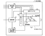
1. 表示装置
図1に、本実施形態における基準電圧発生回路を含む表示駆動回路が適用された表示装置の構成の概要を示す。
【0038】
表示装置(狭義には、電気光学装置、液晶装置)10は、表示パネル(狭義には、液晶パネル)20を含むことができる。
【0039】
表示パネル20は、例えばガラス基板上に形成される。このガラス基板上には、Y方向に複数配列されそれぞれX方向に伸びる走査電極(ゲートライン)G1〜GN(Nは、2以上の自然数)と、X方向に複数配列されそれぞれY方向に伸びる信号電極(ソースライン)S1〜SM(Mは、2以上の自然数)とが配置されている。また、走査電極Gn(1≦n≦N、nは自然数)と信号電極Sm(1≦m≦M、mは自然数)との交差点に対応して、画素領域(画素)が設けられ、該画素領域に薄膜トランジスタ(Thin Film Transistor:以下、TFTと略す。)22nmが配置されている。
【0040】
TFT22nmのゲート電極は、走査電極Gnに接続されている。TFT22nmのソース電極は、信号電極Smに接続されている。TFT22nmのドレイン電極は、液晶容量(広義には液晶素子)24nmの画素電極26nmに接続されている。
【0041】
液晶容量24nmにおいては、画素電極26nmに対向する対向電極28nmとの間に液晶が封入されて形成され、これら電極間の印加電圧に応じて画素の透過率が変化するようになっている。対向電極28nmには、対向電極電圧Vcomが供給される。
【0042】
表示装置10は、信号ドライバIC30を含むことができる。信号ドライバIC30として、本実施形態における表示駆動回路を用いることができる。信号ドライバIC30は、画像データに基づいて、表示パネル20の信号電極S1〜SMを駆動する。
【0043】
表示装置10は、走査ドライバIC32を含むことができる。走査ドライバIC32は、一垂直走査期間内に、表示パネル20の走査電極G1〜GNを順次駆動する。
【0044】
表示装置10は、電源回路34を含むことができる。電源回路34は、信号電極の駆動に必要な電圧を生成し、信号ドライバIC30に対して供給する。また電源回路34は、走査電極の駆動に必要な電圧を生成し、走査ドライバIC32に対して供給する。更に電源回路34は、対向電極電圧Vcomを生成することができる。
【0045】
表示装置10は、コモン電極駆動回路36を含むことができる。コモン電極駆動回路36は、電源回路34によって生成された対向電極電圧Vcomが供給され、該対向電極電圧Vcomを表示パネル20の対向電極に出力する。
【0046】
表示装置10は、信号制御回路38を含むことができる。信号制御回路38は、図示しない中央処理装置(Central Processing Unit:以下、CPUと略す。)等のホストにより設定された内容にしたがって、信号ドライバIC30、走査ドライバIC32、電源回路34を制御する。例えば、信号制御回路38は、信号ドライバIC30及び走査ドライバIC32に対し、動作モードの設定、内部で生成した垂直同期信号や水平同期信号の供給を行い、電源回路34に対し、極性反転タイミングの制御を行う。
【0047】
なお図1では、表示装置10に電源回路34、コモン電極駆動回路36又は信号制御回路38を含めて構成するようにしているが、これらのうち少なくとも1つを表示装置10の外部に設けて構成するようにしてもよい。或いは、表示装置10に、ホストを含めるように構成することも可能である。
【0048】
また図1において、信号ドライバIC30の機能を有する表示駆動回路、及び走査ドライバIC32の機能を有する走査電極駆動回路のうち少なくとも1つを表示パネル20が形成されたガラス基板上に、形成するようにしてもよい。
【0049】
このような構成の表示装置10において、信号ドライバIC30は、階調データに基づく階調表示を行うため、当該階調データに対応した電圧を信号電極に出力するようになっている。信号ドライバIC30は、信号電極に出力する電圧を、階調データに基づいてガンマ補正する。そのため、信号ドライバIC30は、ガンマ補正を行う基準電圧発生回路(狭義には、ガンマ補正回路)を含む。
【0050】
一般に、表示パネル20は、その構造や用いられる液晶材に応じて階調特性が異なる。すなわち、液晶に印加すべき電圧と画素の透過率との関係が一定とはならない。そこで、階調データに応じて液晶に印加すべき最適な電圧を生成するために、基準電圧発生回路によりガンマ補正が行われる。
【0051】
階調データに基づいて選択されて出力される電圧を最適化するため、ガンマ補正では、ラダー抵抗により生成される多値の電圧を補正する。そのとき、表示パネル20の製造メーカ等から指定された電圧を生成するように、ラダー抵抗を構成する抵抗回路の抵抗比が決められる。
【0052】
このようなガンマ補正によれば、駆動対象の表示パネルに最適な電圧を用いて駆動することができる一方、駆動対象の表示パネルごとにラダー抵抗を構成する各抵抗回路の抵抗比を変えて基準電圧発生回路により発生される電圧を変更する必要が生ずる。そのため、駆動対象の表示パネルの種類が異なると、基準電圧発生回路を含む表示駆動回路をも変える必要がある。したがって、表示駆動回路を汎用化することができず、より一層の低コスト化を図ることができなかった。
【0053】
そこで本実施形態では、駆動対象の表示パネルの種類にかかわらず、汎用的に用いることができる基準電圧発生回路と、これを用いた表示駆動回路を提供する。
【0054】
以下では、上述の基準電圧発生回路を含む表示駆動回路が適用された信号ドライバIC30について説明する。
【0055】
2. 信号ドライバIC
図2に、本実施形態における基準電圧発生回路を含む表示駆動回路が適用された信号ドライバIC30の機能ブロック図を示す。
【0056】
信号ドライバIC30は、入力ラッチ回路40、シフトレジスタ42、ラインラッチ回路44、ラッチ回路46、基準電圧選択回路(狭義には、ガンマ補正回路)48、DAC(Digital/Analog Converter)(広義には、電圧選択回路)50、ボルテージフォロワ回路(広義には、信号電極駆動回路)52を含む。
【0057】
入力ラッチ回路40は、図1に示す信号制御回路38から供給される例えば各6ビットのRGB信号からなる階調データを、クロック信号CLKに基づいてラッチする。クロック信号CLKは、信号制御回路38から供給される。
【0058】
入力ラッチ回路40でラッチされた階調データは、シフトレジスタ42において、クロック信号CLKに基づき順次シフトされる。シフトレジスタ42で順次シフトされて入力された階調データは、ラインラッチ回路44に取り込まれる。
【0059】
ラインラッチ回路44に取り込まれた階調データは、ラッチパルス信号LPのタイミングでラッチ回路46にラッチされる。ラッチパルス信号LPは、水平走査周期で入力される。
【0060】
基準電圧発生回路48は、駆動対象の表示パネルの階調表現が最適化されるように決められたラダー抵抗の抵抗比を用いて、高電位側の電源電圧(第1の電源電圧)V0と低電位側の電源電圧(第2の電源電圧)VSSとの間で抵抗分割された分割ノードにおいて発生した多値の基準電圧V0〜VY(Yは、自然数)を出力する。
【0061】
図3に、ガンマ補正の原理を説明するための図を示す。
【0062】
ここでは、液晶の印加電圧に対する画素の透過率の変化を示す階調特性の図を模式的に示す。画素の透過率を0%〜100%(又は100%〜0%)で示すと、一般に液晶の印加電圧が小さくなるほど又は大きくなるほど、透過率の変化が小さくなる。また液晶の印加電圧が中間付近の領域では、透過率の変化が大きくなる。
【0063】
そこで上述の透過率の変化と逆の変化を行うようなガンマ(γ)補正を行うことで、印加電圧に応じてリニアに変化するガンマ補正された透過率を実現させることができる。したがって、ディジタルデータである階調データに基づき、最適化された透過率を実現する基準電圧Vγを生成することができる。すなわち、このような基準電圧が生成されるようにラダー抵抗の抵抗比を実現すればよい。
【0064】
図2における基準電圧発生回路48で生成された多値の基準電圧V0〜VYは、DAC50に供給される。
【0065】
DAC50は、ラッチ回路46から供給された階調データに基づいて、多値の基準電圧V0〜VYのいずれかの電圧を選択して、ボルテージフォロワ回路52に出力する。
【0066】
ボルテージフォロワ回路52は、インピーダンス変換を行って、DAC50から供給された電圧に基づいて信号電極を駆動する。
【0067】
このように信号ドライバIC30は、信号電極ごとに、階調データに基づいて多値の基準電圧の中から選択した電圧を用いて、インピーダンス変換を行って出力する。
【0068】
図4に、ボルテージフォロワ回路52の構成の概要を示す。
【0069】
ここでは、1出力当たりの構成のみを示す。
【0070】
ボルテージフォロワ回路52は、演算増幅器60、第1及び第2のスイッチング素子Q1、Q2を含む。
【0071】
演算増幅器60は、ボルテージフォロワ接続されている。すなわち、演算増幅器60の出力端子が反転入力端子に接続されて、負帰還が構成されている。
【0072】
演算増幅器60の非反転入力端子には、図2に示すDAC50で選択された基準電圧Vinが入力される。演算増幅器60の出力端子は、第1のスイッチング素子Q1を介して、駆動電圧Voutが出力される信号電極に接続される。当該信号電極は、第2のスイッチング素子Q2を介して、演算増幅器60の非反転入力端子にも接続されている。
【0073】
コントロール信号発生回路62は、第1及び第2のスイッチング素子Q1、Q2のオンオフ制御を行うための制御信号VFcntを生成する。このようなコントロール信号発生回路62は、1又は複数の信号電極ごとに設けることができる。
【0074】
第2のスイッチング素子Q2は、制御信号VFcntによりオンオフ制御される。第1のスイッチング素子Q1は、制御信号VFcntが入力されたインバータ回路INV1の出力信号によりオンオフ制御される。
【0075】
図5に、ボルテージフォロワ回路52の動作タイミングの一例を示す。
【0076】
コントロール信号発生回路62により生成された制御信号VFcntは、ラッチパルス信号LPにより規定される選択期間(駆動期間)tの前半期間(駆動期間の初めの所与の期間)t1と後半期間t2で論理レベルが変化する。すなわち、前半期間t1で制御信号VFcntの論理レベルが「L」になると、第1のスイッチング素子Q1がオン、第2のスイッチング素子Q2がオフとなる。また、後半期間t2で制御信号VFcntの論理レベルが「H」になると、第1のスイッチング素子Q1がオフ、第2のスイッチング素子Q2がオンとなる。したがって、選択期間tにおいて、前半期間t1ではボルテージフォロワ接続された演算増幅器60によりインピーダンス変換されて信号電極が駆動され、後半期間t2ではDAC50から出力された基準電圧を用いて信号電極が駆動される。
【0077】
このように駆動することで、液晶容量や配線容量等の充電に必要な前半期間t1では、高い駆動能力を有するボルテージフォロワ接続された演算増幅器60により高速に駆動電圧Voutを立ち上げ、高い駆動能力が不要な後半期間t2では、DAC50により駆動電圧を出力することができる。したがって、電流消費が大きい演算増幅器60の動作期間を最低限に抑え、低消費化を図ることができるとともに、ライン数の増加によって選択期間tが短くなり充電期間が足りなくなるといった事態を回避することができる。
【0078】
図2における基準電圧発生回路48は、駆動対象の表示パネルの階調特性に着目して、ラダー抵抗を構成する各抵抗回路を全て可変にすることなく、その一部の抵抗回路のみ可変制御できるように構成される。これにより、ラダー抵抗の回路規模や制御線の配線、或いは制御自体が簡素化される。。特に多階調化が進むのに伴い、発生すべき基準電圧の多値化が予想されるため、できるだけラダー抵抗の回路規模を増大させることなく、かつ表示パネルに依存せずに汎用化できることが望ましい。
【0079】
更に基準電圧発生回路48は、マスク変更等による配線切替で可変制御を行うのではなく、ユーザからの所与のコマンド又は外部入力端子からの可変制御信号に基づいて、上述のラダー抵抗の可変制御を行う。これにより、信号ドライバIC30を、表示パネルの種類に関わらず汎用的に用いることができる。
【0080】
次に、基準電圧発生回路48について詳細に説明する。
【0081】
3. 基準電圧発生回路
図6に、本実施形態における基準電圧発生回路48の構成の概要を示す。
【0082】
ここでは、本実施形態における基準電圧発生回路48の他に、DAC50と、ボルテージフォロワ回路52とを併せて図示している。
【0083】
基準電圧発生回路48は、高電位側の電源電圧(第1の電源電圧)V0が供給される第1の電源線と低電位側の電源電圧(第2の電源電圧)VSSが供給される第2の電源線との間に接続されたラダー抵抗により、多値の基準電圧V0〜VYを出力する。より具体的には、基準電圧発生回路48は、第1〜第3のラダー抵抗回路70、72、74を含む。第1のラダー抵抗回路70は、その両端部の抵抗値が可変の可変抵抗回路を少なくとも1つ含み、多値の電圧を出力する。第2のラダー抵抗回路72は、抵抗値が固定の複数の抵抗回路が直列接続され、複数の電圧を出力する。第3のラダー抵抗回路74は、その両端部の抵抗値が可変の可変抵抗回路を少なくとも1つ含み、多値の電圧を出力する。
【0084】
第1〜第3のラダー抵抗回路70、72、74は、第1及び第2の電源線の間に直列接続される。より具体的には、一端が第1の電源線に接続された第1のラダー抵抗回路70の他端には、第2のラダー抵抗回路72の一端が接続される。第2のラダー抵抗回路72の他端には、第3のラダー抵抗回路74の一端が接続され、第3のラダー抵抗回路74の他端には第2の電源線が接続される。第1のラダー抵抗回路70は、ラダー抵抗を構成する各抵抗回路の両端の電圧を多値の基準電圧として出力する。第2のラダー抵抗回路72は、ラダー抵抗を構成する各抵抗回路の両端の電圧を多値の基準電圧として出力する。第3のラダー抵抗回路74は、ラダー抵抗を構成する各抵抗回路の両端の電圧を多値の基準電圧として出力する。
【0085】
第1のラダー抵抗回路70に含まれる可変抵抗回路は、例えばユーザから指定された第1のコマンド又は所与の外部入力端子を介して入力された第1の可変制御信号に基づいて抵抗値の可変制御が行われる。第3のラダー抵抗回路74に含まれる可変抵抗回路は、例えばユーザから指定された第2のコマンド又は所与の外部入力端子を介して入力された第2の可変制御信号に基づいて抵抗値の可変制御が行われる。第1及び第3のラダー抵抗回路70、74には、抵抗値が固定の抵抗回路が含まれていてもよいし、全てが可変抵抗回路で構成されていてもよく、少なくとも1つの可変抵抗回路を含んで構成されていればよい。可変抵抗回路は、抵抗素子や、抵抗素子とスイッチ素子等により実現することができる。
【0086】
第1及び第2のコマンドは、同一のコマンドであってもよいし、別個に指定されるコマンドであってもよい。第1及び第2の可変制御信号は、同一の制御信号であってもよいし、別個に入力される制御信号であってもよい。
【0087】
このように基準電圧発生回路48は、第1及び第2の電源線の間に接続されたラダー抵抗のうち、第1及び第2の電源電圧に近い基準電圧を生成するための抵抗回路のみを可変制御する構成となっていることを特徴とする。そのため、ラダー抵抗を構成する全抵抗回路について可変制御を行う必要がなくなるため、制御が容易となり、かつ回路規模の増大を防ぐことができる。
【0088】
基準電圧発生回路48によって生成された多値の基準電圧V0〜VYは、DAC50に供給される。DAC50は、基準電圧の出力ノードごとに設けられたスイッチ回路を有する。各スイッチ回路は、図2に示すラッチ回路46から供給された階調データに基づいて択一的にオン制御される。DAC50は、このようにして選択した電圧を、出力電圧Vinとしてボルテージフォロワ回路52に出力する。
【0089】
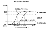
3.1 階調特性
図7に、階調特性について説明するための図を示す。
【0090】
一般に表示パネル、特に液晶パネルは、その構造や液晶材によって階調特性が異なる。したがって、液晶に印加すべき電圧と画素の透過率との関係が一定とはならないことが知られている。図7に示すように、電源電圧が5V系の第1の液晶パネルと、電源電圧が3V系の第2の液晶パネルとを例に挙げると、画素の透過率の変化が大きい能動領域で動作する印加電圧の範囲が異なる。そのため、第1及び第2の液晶パネルそれぞれ別個に、最適な階調表現を実現する電圧に補正するため、ラダー抵抗の抵抗比を決める必要がある。ここで、ラダー抵抗の抵抗比とは、第1及び第2の電源線の間に直列接続されるラダー抵抗の総抵抗値に対する、各抵抗回路の抵抗値の比をいう。
【0091】
図8に、第1及び第2の液晶パネルにおいて、階調値に応じて最適化された基準電圧を示す。
【0092】
ここでは、64階調の各階調値について最適化された基準電圧を、電源電圧を基準とした相対値比で示しており、階調値が最大のとき基準電圧の相対値が「100」になる。図8に示すように、液晶パネルに依存して、補正された基準電圧が異なる。
【0093】
そこで本願出願人は、抵抗値比に着目して解析を進めた結果、以下の通りであることがわかった。ここで抵抗値比とは、ラダー抵抗が直列接続された第1〜第P(Pは、正の整数)の抵抗回路により構成されているものとすると、第1の液晶パネルについて最適化された基準電圧を生成する第L(1≦L≦P、Lは正の整数)の抵抗回路の抵抗値を第1の抵抗値、第2の液晶パネルについて最適化された基準電圧を生成する第Lの抵抗回路の抵抗値を第2の抵抗値とした場合、第2の抵抗値に対する第1の抵抗値の比をいう。
【0094】
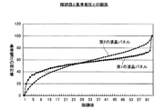
図9に、階調値と第1及び第2の液晶パネルの抵抗値比との関係を示す。
【0095】
ここでは、64階調分の基準電圧を生成するために必要な63個の抵抗値比について示している。抵抗値比に着目すると、高電位側の電源電圧及び低電位側の電源電圧に近い基準電圧を生成する部分80、82では抵抗値比が高くなるが、中間調の部分84の抵抗値比はほぼ「1」であることがわかる。抵抗値比がほぼ「1」の場合、当該階調値に対応した基準電圧を生成するための抵抗値が同等であることを示す。
【0096】
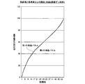
更に、高電位側の電源電圧及び低電位側の電源電圧に近い基準電圧を生成する部分80、82の両端4階調分を削除した場合には、図10に示すように、中間調の基準電圧を生成するための抵抗値はほぼ「1」となることがより顕著となり、中間調の基準電圧を生成するための抵抗回路を共用できることを意味する。
【0097】
そこで、図8に示す第1及び第2の液晶パネルについて、高電位側の電源電圧及び低電位側の電源電圧に近い基準電圧を生成する部分80、82の両端4階調分を削除した場合の階調特性は、図12に示すように中間調においてほぼ一致することが判明した。
【0098】
したがって、ガンマ補正を行うためのラダー抵抗の高電位側及び低電位側の電源電圧に近い数個(例えば4個)ずつの抵抗回路の抵抗値のみを調整することで、異なる種類の液晶パネルに対し最適なガンマ補正を行うことができる基準電圧発生回路を提供することができる。すなわち、ラダー抵抗を構成する全抵抗回路について可変制御を行う必要がない。
【0099】
そこで、図6に示すように、本実施形態における基準電圧発生回路48は、第1及び第3のラダー抵抗回路70、74のみを可変制御し、中間調の基準電圧を生成するための第2のラダー抵抗回路72では抵抗値が固定の抵抗回路のみにより構成する。
【0100】
なお、第2のラダー抵抗回路72を構成する各抵抗回路は、抵抗値比がほぼ「1」の場合のみならず抵抗値比が「2」以下であれば、階調特性を損なうことなく、汎用的な基準電圧発生回路を提供することができる。
【0101】
図12に、基準電圧発生回路48が適用された信号ドライバIC30の具体的な構成の一例を示す。
【0102】
ここでは基準電圧発生回路48が、M本の信号電極の駆動に共用化されている場合を示している。すなわち、M本の信号電極S1 〜SMそれぞれについて、DAC50-1〜50-M、ボルテージフォロワ回路52-1〜52-Mを有している。
【0103】
DAC50-1〜DAC50-Mは、各信号電極に対応する階調データに基づいて、多値の基準電圧の中から1つの基準電圧を選択する。DAC50-1〜50-Mに供給される多値の基準電圧は、基準電圧発生回路48で生成される。基準電圧発生回路48は、第1〜第3のラダー抵抗回路70、72、74を含む。第1及び第3のラダー抵抗回路70、74は、ユーザからのコマンド又は外部入力端子を介して入力された可変制御信号により、ラダー抵抗を構成する抵抗回路の抵抗値が可変制御される。このように構成することで、信号電極数が増加しても、基準電圧発生回路48による回路規模の増大を抑える効果は顕著となる。
【0104】
3.2 ラダー抵抗の可変制御の例
図7に示す階調特性において、所与の透過率tr1、tr2の範囲の透過率の変化の大きい領域を能動領域、それ以外を第1及び第2の非能動領域とする。能動領域は、中間調の階調値に応じた電圧が印加される領域である。第1の非能動領域を、液晶の印加電圧が大きいとき透過率が変化する領域とし、第2の非能動領域を、液晶の印加電圧が小さいとき透過率が変化する領域とする。
【0105】
所与の液晶パネルにおいて、透過率tr2を得るための印加電圧をVA、透過率tr1を得るための印加電圧をVA´(第1の液晶パネルの場合VA=VA1、VA´=VA1´で、第2の液晶パネルの場合VA=VA2、VA´=VA2´)とした場合、第1及び第2の電源電圧の電圧差をVDIFとしたときに、(VDIF−VA)/VDIFが大きいほど、第1及び第3のラダー抵抗回路70、74で可変制御される可変抵抗回路の抵抗値を大きくし、(VDIF−VA)/VDIFが小さいほど、第1及び第3のラダー抵抗回路70、74で可変制御される可変抵抗回路の抵抗値を小さくする。
【0106】
例えば図8に示す第1の液晶パネルの場合に第1及び第3のラダー抵抗回路70、74で可変制御される可変抵抗回路の抵抗値を、第2の液晶パネルの場合に第1及び第3のラダー抵抗回路70、74で可変制御される可変抵抗回路の抵抗値より大きくする。
【0107】
また上述の能動領域が、図9に示す抵抗値比が2以下となることが望ましい。すなわち第2のラダー抵抗回路72では、抵抗値比が2以下となる抵抗回路が直列接続されるように構成することが望ましい。そして、その両端の階調値に対応した基準電圧を生成する第1及び第2のラダー抵抗回路70、74の可変抵抗回路については、上述のように可変制御する。
【0108】
例えば、以上のように可変制御を行うことによって、図6に示す構成の基準電圧発生回路48を含む信号ドライバIC30を、駆動対象の表示パネルに関わらず汎用的に用いることができるようになる。
【0109】
3.3 ラダー抵抗の構成
基準電圧発生回路48において上述のように可変制御される第1及び第3のラダー抵抗回路70、74は、例えば以下のように構成することができる。以下では、第1のラダー抵抗回路70の構成例について説明するが、第3のラダー抵抗回路74も同様に構成することができる。
【0110】
3.3.1 第1の構成例
図13(A)、(B)、(C)に、第1のラダー抵抗回路70の第1の構成例を示す。
【0111】
ここでは第1のラダー抵抗回路70は、図13(A)に示すように例えば直列接続された可変抵抗回路VR0〜VR3を含むもののとする。
【0112】
可変抵抗回路は、図13(B)に示すように、スイッチ回路(スイッチ素子)と抵抗回路(抵抗素子)とが直列接続された抵抗切替回路を並列接続して構成することができる。この場合、並列接続された抵抗切替回路のスイッチ回路では、コマンド若しくは外部入力端子を介して入力される可変制御信号に基づいて、少なくとも1つがオンとなるように制御される。
【0113】
例えば可変抵抗回路VR0は、抵抗切替回路90-01〜90-04を並列接続して構成することができる。可変抵抗回路VR1は、抵抗切替回路90-11〜90-14を並列接続して構成することができる。可変抵抗回路VR2は、抵抗切替回路90-21〜90-24を並列接続して構成することができる。可変抵抗回路VR3は、抵抗切替回路90-31〜90-34を並列接続して構成することができる。
【0114】
また図13(C)に示すように、可変抵抗回路において並列接続された抵抗切替回路に対し、更に抵抗回路を並列接続するようにしてもよい。
【0115】
例えば可変抵抗回路VR0は、抵抗切替回路90-01〜90-04と並列に、抵抗回路92-0を接続して構成することができる。可変抵抗回路VR1は、抵抗切替回路90-11〜90-14と並列に抵抗回路92-1を接続して構成することができる。可変抵抗回路VR2は、抵抗切替回路90-21〜90-24と並列に抵抗回路92-2を接続して構成することができる。可変抵抗回路VR3は、抵抗切替回路90-31〜90-34と並列に抵抗回路92-3を接続して構成することができる。
【0116】
この場合、並列接続された抵抗切替回路のスイッチ回路が少なくとも1つがオンとなるように制御する必要がなくなるので、誤って設定されてオープンとなる状態を回避したり、或いは当該状態を回避する回路を設ける必要がなくなり、構成又は制御が簡素化される。
【0117】
このような構成において、各抵抗切替回路のスイッチ回路は、コマンド若しくは外部入力端子を介して入力される可変制御信号に基づいて、オンオフ制御される。
【0118】
3.3.2 第2の構成例
図14に、第1のラダー抵抗回路70の第2の構成例を示す。
【0119】
ここでは第1のラダー抵抗回路70は、図13(A)に示すように例えば直列接続された可変抵抗回路VR0〜VR3を含むもののとする。
【0120】
可変抵抗回路は、図14に示すように、抵抗回路とスイッチ回路とが並列に接続された抵抗切替回路を直列接続して構成することができる。この場合、抵抗切替回路のスイッチ素子は、コマンド若しくは外部入力端子を介して入力される可変制御信号に基づいて、オンオフ制御される
例えば可変抵抗回路VR0は、抵抗切替回路94-01〜94-04を直列接続して構成することができる。可変抵抗回路VR1は、抵抗切替回路94-11〜94-14を直列接続して構成することができる。可変抵抗回路VR2は、抵抗切替回路94-21〜94-24を直列接続して構成することができる。可変抵抗回路VR3は、抵抗切替回路94-31〜94-34を直列接続して構成することができる。
【0121】
このような構成において、各抵抗切替回路のスイッチ回路は、コマンド若しくは外部入力端子を介して入力される可変制御信号に基づいて、オンオフ制御される。
【0122】
3.3.3 第3の構成例
図15に、第1のラダー抵抗回路70の第3の構成例を示す。
【0123】
ここでは第1のラダー抵抗回路70は、図13(A)に示すように例えば直列接続された可変抵抗回路VR0〜VR3を含むもののとする。
【0124】
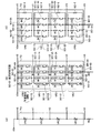
可変抵抗回路VR0では、第1の電源線と分割ノードND1との間に、直列に接続されたスイッチ回路(スイッチ素子)SWA及び抵抗回路R01が挿入されている。分割ノードND1と基準電圧V1の出力ノードとの間には、スイッチ回路SW11が挿入されている。また可変抵抗回路VR0では、第1の電源線とノードND1Bとの間に、直列に接続されたスイッチ回路SWB及び抵抗回路R02が挿入されている。ノードND1Bと基準電圧V1との間には、スイッチ回路SW12が挿入されている。更に可変抵抗回路VR0では、第1の電源線とノードND1Cとの間に、直列に接続されたスイッチ回路SWC及び抵抗回路R03が挿入されている。ノードND1Cと基準電圧V1の出力ノードとの間には、スイッチ回路SW13が挿入されている。
【0125】
可変抵抗回路VR1では、分割ノードND1と分割ノードND2との間に、抵抗回路R11が挿入されている。分割ノードND2と基準電圧V2の出力ノードとの間には、スイッチ回路SW21が挿入されている。また可変抵抗回路VR1では、ノードND1BとノードND2Bとの間に、抵抗回路R12が挿入されている。ノードND2Bと基準電圧V2の出力ノードとの間には、スイッチ回路SW22が挿入されている。更に可変抵抗回路VR1では、ノードND1CとノードND2Cとの間に、抵抗回路R13が挿入されている。ノードND2Cと基準電圧V2の出力ノードとの間には、スイッチ回路SW23が挿入されている。
【0126】
可変抵抗回路VR2では、分割ノードND2と分割ノードND3との間に、抵抗回路R21が挿入されている。分割ノードND3と基準電圧V3の出力ノードとの間には、スイッチ回路SW31が挿入されている。また可変抵抗回路VR2では、ノードND2BとノードND3Bとの間に、抵抗回路R22が挿入されている。ノードND3Bと基準電圧V3の出力ノードとの間には、スイッチ回路SW32が挿入されている。更に可変抵抗回路VR2では、ノードND2CとノードND3Cとの間に、抵抗回路R23が挿入されている。ノードND3Cと基準電圧V3の出力ノードとの間には、スイッチ回路SW33が挿入されている。
【0127】
可変抵抗回路VR3では、分割ノードND3と基準電圧V4の出力ノードとの間に、抵抗回路R31が挿入されている。また可変抵抗回路VR3では、ノードND3Bと基準電圧V4の出力ノードとの間に、抵抗回路R32が挿入されている。更に可変抵抗回路VR3では、ノードND3Cと基準電圧V4の出力ノードとの間に、抵抗回路R33が挿入されている。
【0128】
このような構成において、スイッチ回路SWA、SWB、SWC、SW11〜SW13、SW21〜SW23、SW31〜SW33は、コマンド若しくは外部入力端子を介して入力される可変制御信号に基づいて、オンオフ制御される。
【0129】
例えば、スイッチ回路SWB、SWC、SW13、SW22がオン、スイッチ回路SWA、SW11、SW12、SW21、SW23がオフの場合、基準電圧V1として電源電圧V0が抵抗回路R03により電圧降下した電圧が出力され、基準電圧V2として電源電圧V0から抵抗回路R03と抵抗回路R12とにより電圧降下した電圧が出力される。
【0130】
このように、ラダー抵抗の可変抵抗回路の設定可能な抵抗値をより多様化することができるので、多くの表示パネルに最適化できる基準電圧発生回路を含む信号ドライバICを提供することができるようになる。
【0131】
3.3.4 第4の構成例
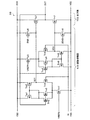
図16に、第1のラダー抵抗回路70の第4の構成例を示す。
【0132】
ここでは第1のラダー抵抗回路70は、図13(A)に示すように例えば直列接続された可変抵抗回路VR0〜VR3を含むもののとする。
【0133】
可変抵抗回路VR0では、第1の電源線と分割ノードND1との間に、抵抗回路R0が挿入されている。また可変抵抗回路VR0では、分割ノードND1と基準電圧V1の出力ノードとの間にボルテージフォロワ回路96-1が挿入されている。ボルテージフォロワ回路96-1は、図4に示したボルテージフォロワ回路と同様の構成をなしており、ボルテージフォロワ回路96-1に含まれる各スイッチ回路は制御信号cnt0、cnt1によりオンオフ制御される。
【0134】
可変抵抗回路VR1では、分割ノードND1と分割ノードND2との間に、抵抗回路R1が挿入されている。また可変抵抗回路VR1では、分割ノードND2と基準電圧V2の出力ノードとの間にボルテージフォロワ回路96-2が挿入されている。ボルテージフォロワ回路96-2は、図4に示したボルテージフォロワ回路と同様の構成をなしており、ボルテージフォロワ回路96-2に含まれる各スイッチ回路は制御信号cnt0、cnt1によりオンオフ制御される。
【0135】
可変抵抗回路VR2では、分割ノードND2と分割ノードND3との間に、抵抗回路R2が挿入されている。また可変抵抗回路VR2では、分割ノードND3と基準電圧V3の出力ノードとの間にボルテージフォロワ回路96-3が挿入されている。ボルテージフォロワ回路96-3は、図4に示したボルテージフォロワ回路と同様の構成をなしており、ボルテージフォロワ回路96-3に含まれる各スイッチ回路は制御信号cnt0、cnt1によりオンオフ制御される。
【0136】
可変抵抗回路VR3では、分割ノードND3と基準電圧V4の出力ノードとの間に、抵抗回路R3が挿入されている。また可変抵抗回路VR3では、ボルテージフォロワ回路96-3のボルテージフォロワ接続された演算増幅器の出力端子と基準電圧V4の出力ノードとの間にオフセット付き演算増幅回路98が挿入されている。演算増幅回路98は、制御信号cnt1により動作制御される(動作電流の制御が行われる)。
【0137】
すなわち、第1〜第R(Rは2以上の整数)の基準電圧のうち第i(1≦i≦R、iは整数)の基準電圧(例えば基準電圧V3)を生成するための第iの分割ノード(例えば分割ノードND3)と第(i−1)の基準電圧を生成するための第(i−1)の分割ノード(例えば分割ノードND2)との間に、抵抗素子(例えば抵抗回路R2)が挿入される。更に、第iの分割ノードにその入力端子が接続されたボルテージフォロワ接続の第1の演算増幅器(例えば、ボルテージフォロワ回路96-3の演算増幅器)と、第iの基準電圧の出力ノードと第1の演算増幅器の出力との間に挿入された第1のスイッチ回路(例えば、ボルテージフォロワ回路96-3の第1のスイッチ素子)と、第iの基準電圧の出力ノードと第iの分割ノードとの間に挿入された第2のスイッチ回路(例えば、ボルテージフォロワ回路96-3の第1のスイッチ素子)とを設ける。
【0138】
そして、第(i+1)の分割ノードと第(i+2)の分割ノードとの間に挿入される抵抗回路の抵抗値が固定の場合、第1の演算増幅器(例えば、ボルテージフォロワ回路96-3の演算増幅器)の出力と第(i+1)の基準電圧の出力ノードとの間に第2の演算増幅回路(例えば、演算増幅回路98)が挿入される。
【0139】
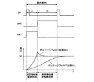
図17に、図16に示した第1のラダー抵抗回路70の制御タイミングの一例を示す。
【0140】
例えば抵抗回路VR0において、ラッチパルス信号LPにより規定される選択期間(駆動期間)tの前半期間(駆動期間の初めの所与の期間)t1と後半期間t2で、制御信号cnt0、cnt1の論理レベルが変化する。すなわち、前半期間t1で制御信号cnt0の論理レベルが「L」、制御信号cnt1の論理レベルが「H」になると、ボルテージフォロワ接続された演算増幅器が基準電圧V1の出力ノードを駆動する。また後半期間t2で、制御信号cnt0の論理レベルが「H」、制御信号cnt1の論理レベルが「L」になると、分割ノードND1と基準電圧V4の出力ノードとが短絡される。したがって、選択期間tにおいて、前半期間t1ではボルテージフォロワ接続された演算増幅器によりインピーダンス変換されて基準電圧V1の出力ノードが駆動され、後半期間t2では抵抗回路R0を介して基準電圧V1の出力ノードの電圧が決まる。
【0141】
すなわち、図17に示すように、液晶容量や配線容量等の充電に必要な前半期間t1では、高い駆動能力を有するボルテージフォロワ接続された演算増幅器により高速に駆動電圧を立ち上げ、高い駆動能力が不要な後半期間t2では、抵抗回路R0により駆動電圧を出力することができる。したがって、ボルテージフォロワ回路によりインピーダンス変換を行うことができるので、第1〜第3の構成例と同様の効果を得ることができる。
【0142】
なおボルテージフォロワ回路96-1〜96-3の演算増幅器については、動作時には動作電流が定常的に流れるため、選択期間tの後半期間t2において、当該動作電流を制限又は停止させることが望ましい。
【0143】
更に可変抵抗回路VR3では、選択期間tの前半期間t1において、演算増幅回路98が基準電圧V3にオフセットを付加した電圧を、基準電圧V4として出力する。
【0144】
同様に、演算増幅回路98についても、選択期間tの後半期間t2において、当該動作電流を制限又は停止させることが望ましい。
【0145】
図18に、演算増幅回路98の詳細な構成例を示す。
【0146】
演算増幅回路98は、差動増幅部100と、出力部102とを含む。
【0147】
差動増幅部100は、第1及び第2の差動増幅部104、106を含む。
【0148】
第1の差動増幅部104は、ゲート電極に基準信号VREFNが印加されるn型MOSトランジスタTrn1(以下、n型MOSトランジスタTrnx(xは任意の整数)を単にTrnxと略す。)のドレイン・ソース間に流れる電流を電流源とし、該電流源はTrn2〜Trn4のソース端子に接続される。Trn2、Trn3のゲート電極には、演算増幅回路98の出力信号OUTが印加されている。Trn4のゲート電極には入力信号INが印加されている。
【0149】
Trn2〜Trn4のドレイン端子は、カレントミラー構造のp型MOSトランジスタTrp1(以下、p型MOSトランジスタTrpy(yは任意の整数)を単にTrpyと略す。)、Trp2のドレイン端子に接続される。なおTrp1、Trp2のゲート電極は、Trn2、Trn3のドレイン端子に接続される。
【0150】
Trp2のドレイン端子から差動出力信号SO1が出力される。
【0151】
第2の差動増幅部106は、ゲート電極に基準信号VREFPが印加されるTTrp3のドレイン・ソース間に流れる電流を電流源とし、該電流源はTrp4〜Trp6のソース端子に接続される。Trp4、Trp5のゲート電極には、演算増幅回路98の出力信号OUTが印加されている。Trp6のゲート電極には入力信号INが印加されている。
【0152】
Trp4〜Trp6のドレイン端子は、カレントミラー構造のTrn5、Trn6のドレイン端子に接続される。なおTrn5、Trn6のゲート電極は、Trp4、Trp5のドレイン端子に接続される。
【0153】
Trn6のドレイン端子から差動出力信号SO2が出力される。
【0154】
出力部102は、電源電圧VDDと接地電源電圧VSSとの間に直列接続されたTrp7とTrn7とを含む。Trp7のゲート電極には、差動出力信号SO1が印加されている。Trn7のゲート電極には、差動出力信号SO2が印加されている。Trp7及びTrn7のドレイン端子から、出力信号OUTが出力される。
【0155】
またTrp7のゲート電極は、Trp8のドレイン端子が接続される。Trp8のソース端子は電源電圧VDDに接続され、ゲート電極にはイネーブル信号ENBが印加される。Trn7のゲート電極は、Trn8のドレイン端子が接続される。Trn8のソース端子は接地電源電圧VSSに接続され、ゲート電極には反転イネーブル信号XENBが印加される。
【0156】
このような構成の演算増幅回路98は、図19に示すように基準信号VREFN、VREFP、イネーブル信号ENB、反転イネーブル信号XENBが動作して、入力信号INの電圧にオフセットを付加した出力信号OUTを出力する。基準信号VREFNとイネーブル信号ENBとして、図16及び図17に示した制御信号cnt1を用いることができる。基準信号VREFPと反転イネーブル信号ENBとして、制御信号cnt1を反転した信号を用いることができる。
【0157】
第1の差動増幅部104において、基準信号VREFNの論理レベルが「H」になりTrn1が電流源として動作を開始すると、出力信号OUTと入力信号INとに基づき、差動対を構成するTrn2、Trn3とTrn4との駆動能力の差に対応した電圧が差動出力信号SO1として出力される。このときTrp8は遮断されるため、差動出力信号SO1がそのままTrp7のゲート電極に印加される。また、第2の差動増幅部106においても、同様にして差動出力信号SO2がTrn7のゲート電極に印加される。その結果、出力部102は、入力信号INに、上述の差動対を構成する駆動能力に対応したオフセットが付加された出力信号OUTを出力することができる。
【0158】
第1の差動増幅部104において、基準信号VREFNの論理レベルが「L」になりTrn1が遮断されると、増幅動作ができなくなり、Trp8を介してTrp7のゲート電極に電源電圧VDDが印加される。同様に、第2の差動増幅部106においても、Trn8を介してTrn7のゲート電極に接地電源電圧VSSが印加される。その結果、出力部102は、その出力をハイインピーダンス状態とする。なお基準信号VREFN、VREFPにより、電流源に流れる電流を制限又は停止することができるので、動作が不要な期間では動作電流が流れないように制御することができる。
【0159】
このようにすることで、演算増幅回路98は、オフセットを高精度に付加することができる。したがって、第4の構成例においては、ボルテージフォロワ回路によるインピーダンス変換を用いて高速に駆動電圧を立ち上げることができる上に、可変抵抗回路の抵抗値を可変制御することができ、表示パネルの種類に関わらず汎用的な基準電圧発生回路を構成することができる。
【0160】
第4の構成例では、可変抵抗回路VR0〜VR3を制御信号cnt0、cnt1で可変制御するものとして説明したが、これに限定されるものではない。可変抵抗回路VR0〜VR3を、別個の制御信号で可変制御するようにしてもよい。
【0161】
4. その他
以上においては、TFTを用いた液晶パネルを備える液晶装置を例に説明したが、これに限定されるものではない。基準電圧発生回路48で生成した基準電圧を、所与の電流変換回路で電流に変えて、電流駆動型の素子に供給するようにしてもよい。このようにすれば、例えば信号電極及び走査電極により特定される画素に対応して設けられた有機EL素子を含む有機ELパネルを表示駆動する信号ドライバICにも適用することができる。
【0162】
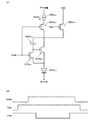
図20に、このような信号ドライバICにより駆動される有機ELパネルにおける2トランジスタ方式の画素回路の一例を示す。
【0163】
有機ELパネルは、信号電極Smと走査電極Gnとの交差点に、駆動TFT800nmと、スイッチTFT810nmと、保持キャパシタ820nmと、有機LED830nmとを有する。駆動TFT800nmは、p型トランジスタにより構成される。
【0164】
駆動TFT800nmと有機LED830nmとは、電源線に直列に接続される。
【0165】
スイッチTFT810nmは、駆動TFT800nmのゲート電極と、信号電極Smとの間に挿入される。スイッチTFT810nmのゲート電極は、走査電極Gnに接続される。
【0166】
保持キャパシタ820nmは、駆動TFT800nmのゲート電極と、キャパシタラインとの間に挿入される。
【0167】
このような有機EL素子において、走査電極Gnが駆動されスイッチTFT810nmがオンになると、信号電極Smの電圧が保持キャパシタ820nmに書き込まれるとともに、駆動TFT800nmのゲート電極に印加される。駆動TFT800nmのゲート電圧Vgsは、信号電極Smの電圧によって決まり、駆動TFT800nmに流れる電流が定まる。駆動TFT800nmと有機LED830nmとは直列接続されているため、駆動TFT800nmに流れる電流がそのまま有機LED830nmに流れる電流となる。
【0168】
したがって、保持キャパシタ820nmにより信号電極Smの電圧に応じたゲート電圧Vgsを保持することによって、例えば1フレーム期間中において、ゲート電圧Vgsに対応した電流を有機LED830nmに流すことで、当該フレームにおいて光り続ける画素を実現することができる。
【0169】
図21(A)に、信号ドライバICを用いて駆動される有機ELパネルにおける4トランジスタ方式の画素回路の一例を示す。図21(B)に、この画素回路の表示制御タイミングの一例を示す。
【0170】
この場合も、有機ELパネルは、駆動TFT900nmと、スイッチTFT910nmと、保持キャパシタ920nmと、有機LED930nmとを有する。
【0171】
図20に示した2トランジスタ方式の画素回路と異なる点は、定電圧の代わりにスイッチ素子としてのp型TFT940nmを介して定電流源950nmからの定電流Idataを画素に供給するようにした点と、電源線にスイッチ素子としてのp型TFT960nmを介して保持キャパシタ920nm及び駆動TFT900nmと接続するようにした点である。
【0172】
このような有機EL素子において、まずゲート電圧Vgpによりp型TFT960をオフにして電源線を遮断し、ゲート電圧Vselによりp型TFT940nmとスイッチTFT910nmをオンにして、定電流源950nmからの定電流Idataを駆動TFT900nmに流す。
【0173】
駆動TFT900nmに流れる電流が安定するまでの間に、保持キャパシタ920nmには定電流Idataに応じた電圧が保持される。
【0174】
続いて、ゲート電圧Vselによりp型TFT940nmとスイッチTFT910nmをオフにし、更にゲート電圧Vgpによりp型TFT960nmをオンにし、電源線と駆動TFT900nm及び有機LED930nmを電気的に接続する。このとき、保持キャパシタ920nmに保持された電圧により、定電流Idataとほぼ同等か、又はこれに応じた大きさの電流が有機LED930nmに供給される。
【0175】
このような有機EL素子では、例えば、走査電極をゲート電圧Vselが印加される電極、信号電極をデータ線として構成することができる。
【0176】
有機LEDは、透明アノード(ITO)の上部に発光層を設け、更にその上部にメタルカソードを設けるようにしても良いし、メタルアノードの上部に、発光層、光透過性カソード、透明シールを設けるようにしても良く、その素子構造に限定されるものではない。
【0177】
以上説明したような有機EL素子を含む有機ELパネルを表示駆動する信号ドライバICを上述したように構成することによって、有機ELパネルについて汎用的に用いられる信号ドライバICを提供することができる。
【0178】
なお、本発明は上述した実施の形態に限定されるものではなく、本発明の要旨の範囲内で種々の変形実施が可能である。例えば、プラズマディスプレイ装置にも適用可能である。
【図面の簡単な説明】
【図1】本実施形態における基準電圧発生回路を含む表示駆動回路が適用された表示装置の構成の概要を示す構成図である。
【図2】基準電圧発生回路を含む表示駆動回路が適用された信号ドライバICの機能ブロック図である。
【図3】ガンマ補正の原理を説明するための説明図である。
【図4】ボルテージフォロワ回路の構成の概要を示すブロック図である。
【図5】ボルテージフォロワ回路の動作タイミングの一例を示すタイミングチャートである。
【図6】本実施形態における基準電圧発生回路の構成の概要を示す回路構成図である。
【図7】階調特性について説明するための説明図である。
【図8】第1及び第2の液晶パネルにおいて、階調値に応じて最適化された基準電圧を示す説明図である。
【図9】階調値と第1及び第2の液晶パネルの抵抗値比との関係を示す説明図である。
【図10】両端4階調ずつ削除した場合の階調値と第1及び第2の液晶パネルの抵抗値比との関係を示す説明図である。
【図11】両端4階調ずつ削除した場合の階調値に応じて最適化された基準電圧を示す説明図である。
【図12】本実施形態における基準電圧発生回路を適用した場合の具体的な回路構成例を示す図である。
【図13】図13(A)、(B)、(C)は、第1の構成例における第1のラダー抵抗回路の回路構成図である。
【図14】第2の構成例における第1のラダー抵抗回路の回路構成図である。
【図15】第3の構成例における第1のラダー抵抗回路の回路構成図である。
【図16】第4の構成例における第1のラダー抵抗回路の回路構成図である。
【図17】第4の構成例における第1のラダー抵抗回路の動作タイミングを示すタイミング図である。
【図18】演算増幅回路の具体的な回路構成例を示す回路図である。
【図19】演算増幅回路の動作制御タイミングを示すタイミング図である。
【図20】有機ELパネルにおける2トランジスタ方式の画素回路の一例を示す構成図である。
【図21】図21(A)は、有機ELパネルにおける4トランジスタ方式の画素回路の一例を示す回路構成図である。図21(B)は、画素回路の表示制御タイミングの一例を示すタイミング図である。
【符号の説明】
10 表示装置(液晶装置)
20 表示パネル(液晶パネル)
22nm TFT
24nm 液晶容量
26nm 画素電極
28nm 対向電極
30 信号ドライバIC(表示駆動回路)
32 走査ドライバIC
34 電源回路
36 コモン電極駆動回路
38 信号制御回路
40 入力ラッチ回路
42 シフトレジスタ
44 ラインラッチ回路
46 ラッチ回路
48 基準電圧発生回路(ガンマ補正回路)
50、50-1、50-2、・・・、50-M DAC(電圧選択回路)
52、52-1、52-2、・・・、52-M、96-1〜96-3 ボルテージフォロワ回路
60 演算増幅器
62 コントロール信号発生回路
70 第1のラダー抵抗回路
72 第2のラダー抵抗回路
74 第3のラダー抵抗回路
90、90-01〜90-04、90-11〜90-14、90-21〜90-24、90-31〜90-34、94-01〜94-04、94-11〜94-14、94-21〜94-24、94-31〜94-34、 抵抗切替回路
92-0〜92-3 抵抗回路
98 演算増幅回路
100 差動増幅部
102 出力部
104 第1の差動増幅部
106 第2の差動増幅部
VR0〜VR3 可変抵抗回路[0001]
BACKGROUND OF THE INVENTION
The present invention provides a reference voltage generation circuit,Display drive circuit and display deviceAbout.
[0002]
[Background Art and Problems to be Solved by the Invention]
A display device typified by an electro-optical device such as a liquid crystal device is required to be small and have high definition. In particular, a liquid crystal device achieves low power consumption and is often mounted on a portable electronic device. For example, when it is mounted as a display unit of a mobile phone, it is required to display an image rich in color tone by increasing the number of gradations.
[0003]
In general, a video signal for image display is subjected to gamma correction according to display characteristics of the display device. This gamma correction is performed by a gamma correction circuit (reference voltage generation circuit in a broad sense). Taking a liquid crystal device as an example, the gamma correction circuit generates a voltage corresponding to the transmittance of the pixel based on the gradation data for performing gradation display.
[0004]
Such a gamma correction circuit is built in a display drive circuit that drives the display device. Therefore, it is desirable that a display drive circuit mounted on an electronic device that is required to be downsized is small. Therefore, the gamma correction circuit is adjusted to perform gamma correction specialized for the display characteristics of the display device to be driven, and a display drive circuit that can be used for general purposes can be provided regardless of the type of the display device. There wasn't.
[0005]
The present invention has been made in view of the technical problems as described above. The object of the present invention is to generate a reference voltage that can be used universally regardless of the type of display device without increasing the circuit scale. circuit,Display drive circuit and display deviceIs to provide.
[0006]
[Means for Solving the Problems]
In order to solve the above-described problems, the present invention provides a reference voltage generation circuit that generates a multi-value reference voltage for generating a gamma-corrected gradation value based on gradation data. A first ladder resistor circuit including at least one variable resistor circuit having a variable resistance value and outputting a multi-value voltage and a plurality of resistor circuits having a fixed resistance value are connected in series to output a plurality of voltages. 2 ladder resistor circuits, and at least one variable resistor circuit having a variable resistance value between both ends thereof, and a third ladder resistor circuit that outputs a multi-value voltage, the first to third The ladder resistor circuit is connected in series between the first and second power supply lines to which the first and second power supply voltages are supplied, and the variable resistor circuit included in the first and third ladder resistor circuits is Based on a given command setting or a given variable control signal Resistance, characterized in that it is variably controlled.
[0007]
In the present invention, first to third ladder resistor circuits are connected in series between the first and second power supply lines, and a multi-valued reference voltage is output from each ladder resistor circuit. The first and third ladder resistor circuits include at least one variable resistor circuit having a variable resistance value between both ends, and the second ladder resistor circuit includes a resistor circuit having a fixed resistance value connected in series. Yes. The first and third ladder resistor circuits are variably controlled by, for example, a given command from a user or a given variable control signal, but the second ladder resistor circuit has a resistance value by a command or a variable control signal. The configuration is not changed.
[0008]
Here, the commands and variable control signals for performing variable control of the first and third ladder resistor circuits may be the same or different.
[0009]
For a display panel, particularly a liquid crystal panel, the reference voltage for performing optimum gradation expression differs depending on the liquid crystal material and the like, and it is necessary to optimize the resistance ratio of the ladder resistance for each type of display panel. However, the region expressing the halftone is almost constant regardless of the type of the display panel. Therefore, according to the present invention, only the resistance values of the first and third ladder resistor circuits are variably controlled by a command or a variable control signal so that the resistance ratio can be changed according to the display panel. Regardless of the type of display panel, a reference voltage subjected to gamma correction can be generated to perform optimum gradation expression while minimizing the increase in circuit scale accompanying control.
[0010]
In the reference voltage generation circuit according to the present invention, the variable resistor circuit included in the first or third ladder resistor circuit may include a resistor switching circuit in which a switch element and a resistor element are connected in series. Good.
[0011]
According to the present invention, various resistance values can be easily realized by controlling the switching elements by connecting the resistance switching circuits in parallel using a resistance switching circuit in which the switching elements and the resistance elements are connected in series. Therefore, a general-purpose reference voltage generation circuit can be provided with a simple configuration as described above.
[0012]
In the reference voltage generation circuit according to the present invention, the variable resistor circuit included in the first or third ladder resistor circuit may include a resistor element connected in parallel with the resistor switching circuit.
[0013]
According to the present invention, since the resistor circuit without the switch element is connected in parallel with the resistor switching circuit, the control or the additional circuit for avoiding the open state by erroneous switch control can be simplified. Can do.
[0014]
In the reference voltage generating circuit according to the present invention, the variable resistor circuit included in the first or third ladder resistor circuit includes a resistor switching circuit including a resistor element and a switch element connected in parallel with the resistor element. It may be connected in series.
[0015]
According to the present invention, the variable resistance circuit is configured by the resistance element and the switch element connected in parallel with the resistance element, and the switch element is controlled to easily realize various resistance values. A general-purpose reference voltage generation circuit can be provided with a simple configuration as described above.
[0016]
In the reference voltage generation circuit according to the present invention, the first or third ladder resistor circuit may have at least two variable resistor circuits and may be connected in series.
[0017]
According to the present invention, the resistance ratio can be controlled with higher accuracy, and a general-purpose reference voltage generation circuit can be provided.
[0018]
In the reference voltage generation circuit according to the present invention, the variable resistor circuit included in the first or third ladder resistor circuit may include the i-th reference voltage among the first to Rth (R is an integer of 2 or more) reference voltages. 1 ≦ i ≦ R, where i is an integer) an i-th (i is a positive integer) split node for generating a reference voltage and an (i−1) th reference voltage for outputting an (i−1) th reference voltage. ), A voltage follower-connected first operational amplifier circuit whose input is connected to the i-th divided node, an output node for the i-th reference voltage, A first switch element inserted between the output of the first operational amplifier circuit and a second switch element inserted between the output node of the i-th reference voltage and the i-th divided node; And the first and second switch elements are in the first half of a given drive period. The first switch element is controlled to be in an on state and the second switch element is controlled to be in an off state. In the second half of the driving period, the first switch element is in an off state and the second switch element is in an on state. The operating current of the first operational amplifier circuit may be limited or stopped in the second half period.
[0019]
According to the present invention, the first operational amplifier circuit can quickly drive a given reference voltage, and the current consumption of the first operational amplifier circuit can be minimized. Therefore, it is possible to provide a reference voltage generation circuit that realizes low power consumption even when the driving period is shortened.
[0020]
The reference voltage generation circuit according to the present invention includes a second operational amplifier circuit inserted between an output of the first operational amplifier circuit and an output node of the (i + 1) th reference voltage, The operational amplifier circuit may output a voltage obtained by adding a given offset voltage to the i-th reference voltage in the first half period, and the operating current may be limited or stopped in the second half period.
[0021]
According to the present invention, for example, the rising of the reference voltage for expressing a halftone can be accelerated by the first operational amplifier circuit and can be driven with high accuracy by the offset added by the second operational amplifier circuit. It becomes possible. Further, the current consumption of the second operational amplifier circuit can be minimized.
[0022]
The reference voltage generation circuit according to the present invention drives the first display panel among the first to Pth resistance circuits (P is a positive integer) constituting the first to third ladder resistance circuits. In this case, the resistance value of the Lth resistance circuit (1 ≦ L ≦ P, L is an integer) is the first resistance value, and the resistance value of the Lth resistance circuit when the second display panel is driven is the second resistance value. When the resistance value is used, the second ladder resistor circuit may be configured by a resistor circuit in which a ratio of the first resistor value to the second resistor value is 2 or less.
[0023]
According to the present invention, it is possible to provide a reference voltage generation circuit that does not depend on the type of the display panel without impairing gradation expression.
[0024]
According to another aspect of the present invention, there is provided a display drive circuit including a voltage selection circuit that selects a voltage based on grayscale data from any of the reference voltage generation circuit described above and a multilevel reference voltage generated by the reference voltage generation circuit. And a signal electrode driving circuit that drives the signal electrode using the voltage selected by the voltage selection circuit.
[0025]
According to the present invention, a display drive circuit including a general-purpose gamma correction circuit can be provided, and cost reduction can be achieved.
[0026]
The display driving circuit according to the present invention may include an external input terminal to which the variable control signal is input.
[0027]
According to the present invention, it is possible to provide a display driving circuit that can be easily adjusted by the user himself / herself in accordance with the display panel.
[0028]
Further, the display device according to the present invention includes a plurality of signal electrodes, a plurality of scanning electrodes intersecting with the plurality of signal electrodes, a pixel specified by the plurality of signal electrodes and the plurality of scanning electrodes, and the plurality of the plurality of signal electrodes. The display driving circuit described above for driving the signal electrode and the scanning electrode driving circuit for driving the plurality of scanning electrodes can be included.
[0029]
According to the present invention, a display device can be provided at low cost by a general-purpose display drive circuit that does not depend on the type of display panel.
[0030]
The display device according to the present invention includes a display including a plurality of signal electrodes, a plurality of scanning electrodes intersecting with the plurality of signal electrodes, and a pixel specified by the plurality of signal electrodes and the plurality of scanning electrodes. The display drive circuit described above for driving the panel, the plurality of signal electrodes, and the scan electrode drive circuit for driving the plurality of scan electrodes can be included.
[0031]
According to the present invention, a display device can be provided at low cost by a general-purpose display drive circuit that does not depend on the type of display panel.
[0032]
The present invention is also a reference voltage generation method for generating a multi-valued reference voltage for generating a gamma-corrected gradation value based on gradation data, wherein the first and second power supply voltages are supplied. Among the first to third ladder resistor circuits connected in series between the first and second power supply lines, the first and third ladder resistor circuits are fixed in a state where the resistance value of the second ladder resistor circuit is fixed. The resistance value of the resistor circuit included in the ladder resistor circuit is variably controlled based on a given command or a variable control signal.
[0033]
According to the present invention, only the resistance values of the first and third ladder resistor circuits are variably controlled by commands and variable control signals so that the resistance ratio can be changed according to the display panel. By the control, it is possible to generate a reference voltage that has been gamma corrected in order to perform optimum gradation expression regardless of the type of the display panel.
[0034]
DETAILED DESCRIPTION OF THE INVENTION
DESCRIPTION OF EMBODIMENTS Hereinafter, preferred embodiments of the present invention will be described in detail with reference to the drawings. The embodiment described below does not unduly limit the contents of the present invention described in the claims. Also, not all of the configurations described below are essential constituent requirements of the present invention.
[0035]
The reference voltage generation circuit in this embodiment can be used as a gamma correction circuit. This gamma correction circuit is included in the display drive circuit. The display driving circuit can be used for driving an electro-optical device that changes optical characteristics according to an applied voltage, for example, a liquid crystal device.
[0036]
Hereinafter, the case where the reference voltage generation circuit according to this embodiment is applied to a liquid crystal device will be described, but the present invention is not limited to this, and can be applied to other display devices.
[0037]
1. Display device
FIG. 1 shows an outline of the configuration of a display device to which a display drive circuit including a reference voltage generation circuit according to this embodiment is applied.
[0038]
The display device (in a narrow sense, an electro-optical device, a liquid crystal device) 10 can include a display panel (in a narrow sense, a liquid crystal panel) 20.
[0039]
The
[0040]
TFT22nmThe gate electrode of the scanning electrode GnIt is connected to the. TFT22nmThe source electrode of the signal electrode SmIt is connected to the. TFT22nmThe drain electrode is a liquid crystal capacitor (liquid crystal element in a broad sense) 24.nmPixel electrode 26nmIt is connected to the.
[0041]
Liquid crystal capacity 24nmIn the pixel electrode 26,nmCounter electrode 28 facingnmA liquid crystal is sealed between the electrodes, and the transmittance of the pixel changes according to the voltage applied between the electrodes. Counter electrode 28nmIs supplied with a counter electrode voltage Vcom.
[0042]
The display device 10 can include a
[0043]
The display device 10 can include a
[0044]
The display device 10 can include a
[0045]
The display device 10 can include a common
[0046]
The display device 10 can include a
[0047]
In FIG. 1, the display device 10 includes the
[0048]
In FIG. 1, at least one of a display drive circuit having the function of the
[0049]
In the display device 10 having such a configuration, the
[0050]
In general, the
[0051]
In order to optimize the voltage selected and output based on the gradation data, the multi-value voltage generated by the ladder resistor is corrected in the gamma correction. At that time, the resistance ratio of the resistor circuit constituting the ladder resistor is determined so as to generate a voltage specified by the manufacturer of the
[0052]
According to such gamma correction, it is possible to drive the display panel to be driven using an optimum voltage, while changing the resistance ratio of each resistance circuit constituting the ladder resistor for each display panel to be driven to change the reference. It becomes necessary to change the voltage generated by the voltage generation circuit. Therefore, if the type of display panel to be driven is different, it is necessary to change the display drive circuit including the reference voltage generation circuit. Therefore, the display drive circuit cannot be generalized, and further cost reduction cannot be achieved.
[0053]
Therefore, in the present embodiment, a reference voltage generation circuit that can be used universally regardless of the type of display panel to be driven, and a display drive circuit using the reference voltage generation circuit are provided.
[0054]
Hereinafter, the
[0055]
2. Signal driver IC
FIG. 2 is a functional block diagram of the
[0056]
The
[0057]
The
[0058]
The gradation data latched by the
[0059]
The gradation data fetched by the
[0060]
The reference
[0061]
FIG. 3 is a diagram for explaining the principle of gamma correction.
[0062]
Here, a diagram of gradation characteristics showing a change in transmittance of a pixel with respect to an applied voltage of liquid crystal is schematically shown. When the transmittance of a pixel is represented by 0% to 100% (or 100% to 0%), generally, the change in transmittance decreases as the applied voltage of the liquid crystal decreases or increases. In the region where the applied voltage of the liquid crystal is near the middle, the change in transmittance is large.
[0063]
Therefore, by performing gamma (γ) correction that performs a change opposite to the above-described change in transmittance, it is possible to realize a gamma-corrected transmittance that changes linearly according to the applied voltage. Therefore, it is possible to generate the reference voltage Vγ that realizes the optimized transmittance based on the gradation data that is digital data. That is, the resistance ratio of the ladder resistor may be realized so that such a reference voltage is generated.
[0064]
Multi-valued reference voltages V0 to VY generated by the reference
[0065]
The
[0066]
The
[0067]
As described above, the
[0068]
FIG. 4 shows an outline of the configuration of the
[0069]
Here, only the configuration per output is shown.
[0070]
The
[0071]
The
[0072]
The reference voltage Vin selected by the
[0073]
The control
[0074]
The second switching element Q2 is on / off controlled by a control signal VFcnt. The first switching element Q1 is ON / OFF controlled by the output signal of the inverter circuit INV1 to which the control signal VFcnt is input.
[0075]
FIG. 5 shows an example of the operation timing of the
[0076]
The control signal VFcnt generated by the control
[0077]
By driving in this way, in the first half period t1 necessary for charging the liquid crystal capacitance, wiring capacitance, etc., the driving voltage Vout is raised at high speed by the
[0078]
The reference
[0079]
Furthermore, the reference
[0080]
Next, the reference
[0081]
3. Reference voltage generation circuit
FIG. 6 shows an outline of the configuration of the reference
[0082]
Here, in addition to the reference
[0083]
The reference
[0084]
The first to third
[0085]
The variable resistance circuit included in the first
[0086]
The first and second commands may be the same command, or may be commands specified separately. The first and second variable control signals may be the same control signal, or may be control signals that are input separately.
[0087]
As described above, the reference
[0088]
The multi-level reference voltages V0 to VY generated by the reference
[0089]
3.1 Tone characteristics
FIG. 7 is a diagram for explaining the gradation characteristics.
[0090]
In general, a display panel, particularly a liquid crystal panel, has different gradation characteristics depending on its structure and liquid crystal material. Therefore, it is known that the relationship between the voltage to be applied to the liquid crystal and the transmittance of the pixel is not constant. As shown in FIG. 7, for example, a first liquid crystal panel with a power supply voltage of 5V and a second liquid crystal panel with a power supply voltage of 3V are used in an active region where the change in transmittance of pixels is large. The range of applied voltage differs. Therefore, it is necessary to determine the resistance ratio of the ladder resistor in order to correct the voltage to achieve the optimum gradation expression separately for each of the first and second liquid crystal panels. Here, the resistance ratio of the ladder resistor refers to the ratio of the resistance value of each resistor circuit to the total resistance value of the ladder resistor connected in series between the first and second power supply lines.
[0091]
FIG. 8 shows a reference voltage optimized in accordance with the gradation value in the first and second liquid crystal panels.
[0092]
Here, the reference voltage optimized for each gradation value of 64 gradations is shown as a relative value ratio based on the power supply voltage. When the gradation value is the maximum, the relative value of the reference voltage is “100”. Become. As shown in FIG. 8, the corrected reference voltage differs depending on the liquid crystal panel.
[0093]
Therefore, as a result of the analysis of the applicant of the present application focusing on the resistance value ratio, it was found that the following was obtained. Here, the resistance value ratio is optimized for the first liquid crystal panel, assuming that the resistance value ratio is configured by first to Pth resistance circuits (P is a positive integer) in which ladder resistors are connected in series. The resistance value of the Lth resistor circuit (1 ≦ L ≦ P, L is a positive integer) that generates the reference voltage is the first resistance value, and the Lth circuit that generates the reference voltage optimized for the second liquid crystal panel. When the resistance value of the resistor circuit is the second resistance value, it means the ratio of the first resistance value to the second resistance value.
[0094]
FIG. 9 shows the relationship between the gradation value and the resistance value ratio of the first and second liquid crystal panels.
[0095]
Here, 63 resistance value ratios necessary for generating reference voltages for 64 gradations are shown. Focusing on the resistance value ratio, the resistance value ratio is high in the
[0096]
Furthermore, when the four gradations at both ends of the
[0097]
Therefore, in the first and second liquid crystal panels shown in FIG. 8, when the four gradations at both ends of the
[0098]
Therefore, by adjusting only the resistance values of several resistance circuits (for example, four) close to the power supply voltage on the high potential side and the low potential side of the ladder resistor for performing gamma correction, different types of liquid crystal panels can be obtained. Thus, it is possible to provide a reference voltage generation circuit capable of performing an optimal gamma correction. That is, it is not necessary to perform variable control for all the resistance circuits constituting the ladder resistor.
[0099]
Therefore, as shown in FIG. 6, the reference
[0100]
Each of the resistance circuits constituting the second
[0101]
FIG. 12 shows an example of a specific configuration of the
[0102]
Here, a case is shown in which the reference
[0103]
The DAC 50-1 to DAC 50-M select one reference voltage from among multi-valued reference voltages based on the gradation data corresponding to each signal electrode. Multi-valued reference voltages supplied to the DACs 50-1 to 50-M are generated by a reference
[0104]
3.2 Example of variable control of ladder resistance
In the gradation characteristics shown in FIG. 7, an area having a large change in transmittance in a range of given transmittances tr1 and tr2 is defined as an active area, and the other areas are defined as first and second inactive areas. The active area is an area to which a voltage corresponding to a halftone gradation value is applied. The first inactive region is a region where the transmittance changes when the applied voltage of the liquid crystal is large, and the second inactive region is a region where the transmittance changes when the applied voltage of the liquid crystal is small.
[0105]
In a given liquid crystal panel, the applied voltage for obtaining the transmittance tr2 is VA, and the applied voltage for obtaining the transmittance tr1 is VA ′ (in the case of the first liquid crystal panel, VA = VA1, VA ′ = VA1 ′, In the case of the second liquid crystal panel VA = VA2, VA ′ = VA2 ′), when the voltage difference between the first and second power supply voltages is VDIF, the larger (VDIF−VA) / VDIF is, The resistance values of the variable resistor circuits variably controlled by the first and third
[0106]
For example, in the case of the first liquid crystal panel shown in FIG. 8, the resistance value of the variable resistor circuit variably controlled by the first and third
[0107]
Moreover, it is desirable that the resistance value ratio shown in FIG. That is, it is desirable that the second
[0108]
For example, by performing variable control as described above, the
[0109]
3.3 Configuration of ladder resistor
The first and third
[0110]
3.3.1 First configuration example
FIGS. 13A, 13 </ b> B, and 13 </ b> C show a first configuration example of the first
[0111]
Here, it is assumed that the first
[0112]
As shown in FIG. 13B, the variable resistance circuit can be configured by connecting in parallel a resistance switching circuit in which a switch circuit (switch element) and a resistance circuit (resistance element) are connected in series. In this case, the switch circuits of the resistance switching circuits connected in parallel are controlled so that at least one is turned on based on a command or a variable control signal input via an external input terminal.
[0113]
For example, the variable resistance circuit VR0 can be configured by connecting resistance switching circuits 90-01 to 90-04 in parallel. The variable resistance circuit VR1 can be configured by connecting resistance switching circuits 90-11 to 90-14 in parallel. The variable resistance circuit VR2 can be configured by connecting resistance switching circuits 90-21 to 90-24 in parallel. The variable resistance circuit VR3 can be configured by connecting resistance switching circuits 90-31 to 90-34 in parallel.
[0114]
Further, as shown in FIG. 13C, a resistance circuit may be further connected in parallel to the resistance switching circuit connected in parallel in the variable resistance circuit.
[0115]
For example, the variable resistance circuit VR0 can be configured by connecting a resistance circuit 92-0 in parallel with the resistance switching circuits 90-01 to 90-04. The variable resistance circuit VR1 can be configured by connecting a resistance circuit 92-1 in parallel with the resistance switching circuits 90-11 to 90-14. The variable resistance circuit VR2 can be configured by connecting a resistance circuit 92-2 in parallel with the resistance switching circuits 90-21 to 90-24. The variable resistance circuit VR3 can be configured by connecting a resistance circuit 92-3 in parallel with the resistance switching circuits 90-31 to 90-34.
[0116]
In this case, since it is not necessary to control at least one switch circuit of the resistance switching circuit connected in parallel to be turned on, a circuit that avoids an erroneously set state or an open state, or a circuit that avoids the state This eliminates the need to provide a configuration and control.
[0117]
In such a configuration, the switch circuit of each resistance switching circuit is ON / OFF controlled based on a command or a variable control signal input via an external input terminal.
[0118]
3.3.2 Second configuration example
FIG. 14 shows a second configuration example of the first
[0119]
Here, it is assumed that the first
[0120]
As shown in FIG. 14, the variable resistance circuit can be configured by connecting in series a resistance switching circuit in which a resistance circuit and a switch circuit are connected in parallel. In this case, the switch element of the resistance switching circuit is ON / OFF controlled based on a command or a variable control signal input via an external input terminal.
For example, the variable resistance circuit VR0 can be configured by connecting resistance switching circuits 94-01 to 94-04 in series. The variable resistance circuit VR1 can be configured by connecting resistance switching circuits 94-11 to 94-14 in series. The variable resistance circuit VR2 can be configured by connecting resistance switching circuits 94-21 to 94-24 in series. The variable resistance circuit VR3 can be configured by connecting resistance switching circuits 94-31 to 94-34 in series.
[0121]
In such a configuration, the switch circuit of each resistance switching circuit is ON / OFF controlled based on a command or a variable control signal input via an external input terminal.
[0122]
3.3.3 Third configuration example
FIG. 15 shows a third configuration example of the first
[0123]
Here, it is assumed that the first
[0124]
In the variable resistance circuit VR0, a switch circuit (switch element) SWA and a resistance circuit R connected in series between the first power supply line and the divided node ND1.01Has been inserted. A switch circuit SW is provided between the divided node ND1 and the output node of the reference voltage V1.11Has been inserted. In the variable resistance circuit VR0, the switch circuit SWB and the resistance circuit R connected in series between the first power supply line and the node ND1B.02Has been inserted. A switch circuit SW is connected between the node ND1B and the reference voltage V1.12Has been inserted. Further, in the variable resistance circuit VR0, the switch circuit SWC and the resistance circuit R connected in series between the first power supply line and the node ND1C.03Has been inserted. A switch circuit SW is connected between the node ND1C and the output node of the reference voltage V1.13Has been inserted.
[0125]
In the variable resistance circuit VR1, a resistance circuit R is provided between the divided node ND1 and the divided node ND2.11Has been inserted. A switch circuit SW is provided between the divided node ND2 and the output node of the reference voltage V2.twenty oneHas been inserted. In the variable resistance circuit VR1, the resistance circuit R is connected between the node ND1B and the node ND2B.12Has been inserted. A switch circuit SW is connected between the node ND2B and the output node of the reference voltage V2.twenty twoHas been inserted. Further, in the variable resistance circuit VR1, the resistance circuit R is provided between the node ND1C and the node ND2C.13Has been inserted. A switch circuit SW is connected between the node ND2C and the output node of the reference voltage V2.twenty threeHas been inserted.
[0126]
In the variable resistance circuit VR2, a resistance circuit R is provided between the divided node ND2 and the divided node ND3.twenty oneHas been inserted. A switch circuit SW is provided between the divided node ND3 and the output node of the reference voltage V3.31Has been inserted. In the variable resistance circuit VR2, the resistance circuit R is provided between the node ND2B and the node ND3B.twenty twoHas been inserted. A switch circuit SW is connected between the node ND3B and the output node of the reference voltage V3.32Has been inserted. Further, in the variable resistance circuit VR2, the resistance circuit R is provided between the node ND2C and the node ND3C.twenty threeHas been inserted. A switch circuit SW is connected between the node ND3C and the output node of the reference voltage V3.33Has been inserted.
[0127]
In the variable resistance circuit VR3, the resistance circuit R is provided between the divided node ND3 and the output node of the reference voltage V4.31Has been inserted. In the variable resistance circuit VR3, the resistance circuit R is connected between the node ND3B and the output node of the reference voltage V4.32Has been inserted. Further, in the variable resistance circuit VR3, the resistance circuit R is connected between the node ND3C and the output node of the reference voltage V4.33Has been inserted.
[0128]
In such a configuration, the switch circuits SWA, SWB, SWC, SW11~ SW13, SWtwenty one~ SWtwenty three, SW31~ SW33Is controlled on and off based on a variable control signal input via a command or an external input terminal.
[0129]
For example, switch circuits SWB, SWC, SW13, SWtwenty twoIs ON, switch circuit SWA, SW11, SW12, SWtwenty one, SWtwenty threeIs off, the power supply voltage V0 is used as the reference voltage V1 in the resistance circuit R.03Is output from the power supply voltage V0 as the reference voltage V2.03And resistance circuit R12As a result, the voltage dropped is output.
[0130]
As described above, since the variable resistance values of the variable resistance circuit of the ladder resistor can be further diversified, it is possible to provide a signal driver IC including a reference voltage generation circuit that can be optimized for many display panels. become.
[0131]
3.3.4 Fourth configuration example
FIG. 16 shows a fourth configuration example of the first
[0132]
Here, it is assumed that the first
[0133]
In the variable resistance circuit VR0, the resistance circuit R0 is inserted between the first power supply line and the divided node ND1. In the variable resistance circuit VR0, a voltage follower circuit 96-1 is inserted between the divided node ND1 and the output node of the reference voltage V1. The voltage follower circuit 96-1 has the same configuration as that of the voltage follower circuit shown in FIG. 4, and each switch circuit included in the voltage follower circuit 96-1 is ON / OFF controlled by control signals cnt0 and cnt1.
[0134]
In the variable resistance circuit VR1, the resistance circuit R1 is inserted between the divided node ND1 and the divided node ND2. In the variable resistance circuit VR1, a voltage follower circuit 96-2 is inserted between the divided node ND2 and the output node of the reference voltage V2. The voltage follower circuit 96-2 has the same configuration as that of the voltage follower circuit shown in FIG. 4, and each switch circuit included in the voltage follower circuit 96-2 is ON / OFF controlled by control signals cnt0 and cnt1.
[0135]
In the variable resistance circuit VR2, the resistance circuit R2 is inserted between the divided node ND2 and the divided node ND3. In the variable resistance circuit VR2, a voltage follower circuit 96-3 is inserted between the divided node ND3 and the output node of the reference voltage V3. The voltage follower circuit 96-3 has the same configuration as the voltage follower circuit shown in FIG. 4, and each switch circuit included in the voltage follower circuit 96-3 is ON / OFF controlled by control signals cnt0 and cnt1.
[0136]
In the variable resistance circuit VR3, the resistance circuit R3 is inserted between the divided node ND3 and the output node of the reference voltage V4. In the variable resistance circuit VR3, an
[0137]
That is, the i-th reference voltage (for example, the reference voltage V3) for generating the i-th (1 ≦ i ≦ R, i is an integer) reference voltage among the first to R-th (R is an integer of 2 or more) reference voltages. A resistive element (eg, resistance circuit R2) is provided between the division node (eg, division node ND3) and the (i−1) th division node (eg, division node ND2) for generating the (i−1) th reference voltage. ) Is inserted. In addition, a voltage follower-connected first operational amplifier whose input terminal is connected to the i-th divided node (for example, an operational amplifier of the voltage follower circuit 96-3), an output node of the i-th reference voltage, and a first A first switch circuit (for example, a first switch element of the voltage follower circuit 96-3), an output node of the i-th reference voltage, an i-th divided node, And a second switch circuit (for example, a first switch element of the voltage follower circuit 96-3) inserted between the two.
[0138]
When the resistance value of the resistance circuit inserted between the (i + 1) th divided node and the (i + 2) th divided node is fixed, the operation of the first operational amplifier (for example, the voltage follower circuit 96-3) A second operational amplifier circuit (for example, operational amplifier circuit 98) is inserted between the output of the amplifier) and the output node of the (i + 1) th reference voltage.
[0139]
FIG. 17 shows an example of the control timing of the first
[0140]
For example, in the resistance circuit VR0, the logic levels of the control signals cnt0 and cnt1 are generated in the first half period (a given period at the beginning of the drive period) t1 and the second half period t2 of the selection period (drive period) t defined by the latch pulse signal LP. Changes. That is, when the logic level of the control signal cnt0 becomes “L” and the logic level of the control signal cnt1 becomes “H” in the first half period t1, the operational amplifier connected to the voltage follower drives the output node of the reference voltage V1. In the second half period t2, when the logic level of the control signal cnt0 becomes “H” and the logic level of the control signal cnt1 becomes “L”, the divided node ND1 and the output node of the reference voltage V4 are short-circuited. Therefore, in the selection period t, in the first half period t1, impedance conversion is performed by the operational amplifier connected to the voltage follower to drive the output node of the reference voltage V1, and in the second half period t2, the output node of the reference voltage V1 is connected via the resistor circuit R0. The voltage is determined.
[0141]
That is, as shown in FIG. 17, in the first half period t1 required for charging the liquid crystal capacitance, wiring capacitance, etc., the driving voltage is raised at high speed by the operational amplifier connected to the voltage follower having high driving capability, and the high driving capability is obtained. In the unnecessary second half period t2, the driving voltage can be output by the resistor circuit R0. Therefore, since impedance conversion can be performed by the voltage follower circuit, the same effects as those of the first to third configuration examples can be obtained.
[0142]
In the operational amplifiers of the voltage follower circuits 96-1 to 96-3, the operating current constantly flows during operation. Therefore, it is desirable to limit or stop the operating current in the second half period t2 of the selection period t.
[0143]
Further, in the variable resistance circuit VR3, in the first half period t1 of the selection period t, the
[0144]
Similarly, for the
[0145]
FIG. 18 shows a detailed configuration example of the
[0146]
The
[0147]
The
[0148]
The first differential amplifying unit 104 includes a drain of an n-type MOS transistor Trn1 (hereinafter, n-type MOS transistor Trnx (x is an arbitrary integer) is simply abbreviated as Trnx) to which a reference signal VREFN is applied to a gate electrode. A current flowing between the sources is used as a current source, and the current source is connected to the source terminals of Trn2 to Trn4. The output signal OUT of the
[0149]
The drain terminals of Trn2 to Trn4 are connected to the drain terminal of a p-type MOS transistor Trp1 (hereinafter, p-type MOS transistor Trpy (y is an arbitrary integer) is simply abbreviated as Trpy) having a current mirror structure, and Trp2. The gate electrodes of Trp1 and Trp2 are connected to the drain terminals of Trn2 and Trn3.
[0150]
A differential output signal SO1 is output from the drain terminal of Trp2.
[0151]
The second differential amplifier 106 uses a current flowing between the drain and source of TTrp3 to which the reference signal VREFP is applied to the gate electrode as a current source, and the current source is connected to the source terminals of Trp4 to Trp6. The output signal OUT of the
[0152]
The drain terminals of Trp4 to Trp6 are connected to the drain terminals of Trn5 and Trn6 having a current mirror structure. The gate electrodes of Trn5 and Trn6 are connected to the drain terminals of Trp4 and Trp5.
[0153]
A differential output signal SO2 is output from the drain terminal of Trn6.
[0154]
The output unit 102 includes Trp7 and Trn7 connected in series between the power supply voltage VDD and the ground power supply voltage VSS. A differential output signal SO1 is applied to the gate electrode of Trp7. A differential output signal SO2 is applied to the gate electrode of Trn7. An output signal OUT is output from the drain terminals of Trp7 and Trn7.
[0155]
The gate electrode of Trp7 is connected to the drain terminal of Trp8. The source terminal of Trp8 is connected to the power supply voltage VDD, and the enable signal ENB is applied to the gate electrode. The gate electrode of Trn7 is connected to the drain terminal of Trn8. The source terminal of Trn8 is connected to the ground power supply voltage VSS, and the inverted enable signal XENB is applied to the gate electrode.
[0156]
As shown in FIG. 19, the
[0157]
In the first differential amplifier 104, when the logic level of the reference signal VREFN becomes “H” and Trn1 starts operating as a current source, Trn2 that forms a differential pair based on the output signal OUT and the input signal IN , A voltage corresponding to the difference in driving capability between Trn3 and Trn4 is output as a differential output signal SO1. At this time, since Trp8 is cut off, the differential output signal SO1 is directly applied to the gate electrode of Trp7. Similarly, in the second differential amplifier 106, the differential output signal SO2 is applied to the gate electrode of Trn7. As a result, the output unit 102 can output the output signal OUT obtained by adding an offset corresponding to the driving capability of the differential pair described above to the input signal IN.
[0158]
In the first differential amplifier 104, when the logic level of the reference signal VREFN becomes “L” and Trn1 is cut off, the amplification operation cannot be performed, and the power supply voltage VDD is applied to the gate electrode of Trp7 via Trp8. The Similarly, in the second differential amplifier 106, the ground power supply voltage VSS is applied to the gate electrode of Trn7 via Trn8. As a result, the output unit 102 sets the output to a high impedance state. Note that since the current flowing through the current source can be limited or stopped by the reference signals VREFN and VREFP, the operation current can be controlled not to flow during a period when the operation is unnecessary.
[0159]
By doing so, the
[0160]
In the fourth configuration example, the variable resistance circuits VR0 to VR3 are variably controlled by the control signals cnt0 and cnt1, but the present invention is not limited to this. The variable resistance circuits VR0 to VR3 may be variably controlled with separate control signals.
[0161]
4). Other
In the above, a liquid crystal device including a liquid crystal panel using TFTs has been described as an example. However, the present invention is not limited to this. The reference voltage generated by the reference
[0162]
FIG. 20 shows an example of a two-transistor pixel circuit in an organic EL panel driven by such a signal driver IC.
[0163]
The organic EL panel has a signal electrode SmAnd scan electrode GnDriving TFT 800 at the intersection withnmAnd switch TFT810nmAnd holding capacitor 820nmAnd organic LED830nmAnd have. Driving TFT 800nmIs constituted by a p-type transistor.
[0164]
Driving TFT 800nmAnd organic LED830nmIs connected in series with the power line.
[0165]
Switch TFT810nmThe driving TFT 800nmGate electrode and signal electrode SmInserted between. Switch TFT810nmThe gate electrode of the scanning electrode GnConnected to.
[0166]
Holding capacitor 820nmThe driving TFT 800nmBetween the gate electrode and the capacitor line.
[0167]
In such an organic EL element, the scanning electrode GnIs driven to switch TFT810nmIs turned on, the signal electrode SmIs the holding capacitor 820nmAnd driving TFT 800nmApplied to the gate electrode. Driving TFT 800nmThe gate voltage Vgs of the signal electrode SmDepends on the voltage of the driving TFT 800nmThe current that flows through is determined. Driving TFT 800nmAnd organic LED830nmIs connected in series with the driving TFT 800nmThe current that flows through the organic LED 830nmThe current that flows in
[0168]
Therefore, holding capacitor 820nmSignal electrode SmFor example, during one frame period, a current corresponding to the gate voltage Vgs is supplied to the organic LED 830 by holding the gate voltage Vgs according to the voltage ofnmThe pixel that continues to shine in the frame can be realized.
[0169]
FIG. 21A shows an example of a 4-transistor pixel circuit in an organic EL panel driven using a signal driver IC. FIG. 21B shows an example of the display control timing of this pixel circuit.
[0170]
Also in this case, the organic EL panel has a driving TFT 900.nmAnd switch TFT 910nmAnd holding capacitor 920nmAnd organic LED 930nmAnd have.
[0171]
A difference from the two-transistor pixel circuit shown in FIG. 20 is that a p-type TFT 940 as a switching element instead of a constant voltage is used.nmThrough a constant current source 950nmAnd a p-type TFT 960 as a switch element on the power line.nmThrough the holding capacitor 920nmAnd driving TFT 900nmIt is a point to connect with.
[0172]
In such an organic EL element, first, the p-type TFT 960 is turned off by the gate voltage Vgp to cut off the power supply line, and the p-type TFT 940 is cut by the gate voltage Vsel.nmAnd switch TFT910nmAnd turn on the constant current source 950nmThe constant current Idata from the drive TFT 900nmShed.
[0173]
Driving TFT900nmUntil the current flowing through the capacitor stabilizes, the holding capacitor 920nmHolds a voltage corresponding to the constant current Idata.
[0174]
Subsequently, the p-type TFT 940 is driven by the gate voltage Vsel.nmAnd switch TFT910nmAnd p-type TFT 960 by gate voltage Vgp.nmTurn on the power line and driving TFT900nmAnd organic LED 930nmAre electrically connected. At this time, the holding capacitor 920nmDue to the voltage held in the organic LED 930, a current substantially equal to the constant current Idata or a magnitude corresponding to the constant current Idata is obtained.nmTo be supplied.
[0175]
In such an organic EL element, for example, the scanning electrode can be configured as an electrode to which the gate voltage Vsel is applied, and the signal electrode can be configured as a data line.
[0176]
In the organic LED, a light emitting layer may be provided on the transparent anode (ITO), and a metal cathode may be provided on the light emitting layer. A light emitting layer, a light transmitting cathode, and a transparent seal may be provided on the metal anode. However, the present invention is not limited to the element structure.
[0177]
By configuring the signal driver IC for displaying and driving the organic EL panel including the organic EL element as described above as described above, it is possible to provide a signal driver IC for general use with respect to the organic EL panel.
[0178]
The present invention is not limited to the above-described embodiment, and various modifications can be made within the scope of the gist of the present invention. For example, the present invention can be applied to a plasma display device.
[Brief description of the drawings]
FIG. 1 is a configuration diagram showing an outline of a configuration of a display device to which a display drive circuit including a reference voltage generation circuit according to an embodiment is applied.
FIG. 2 is a functional block diagram of a signal driver IC to which a display drive circuit including a reference voltage generation circuit is applied.
FIG. 3 is an explanatory diagram for explaining the principle of gamma correction.
FIG. 4 is a block diagram showing an outline of a configuration of a voltage follower circuit.
FIG. 5 is a timing chart illustrating an example of operation timing of the voltage follower circuit.
FIG. 6 is a circuit configuration diagram showing an outline of a configuration of a reference voltage generation circuit in the present embodiment.
FIG. 7 is an explanatory diagram for explaining gradation characteristics.
FIG. 8 is an explanatory diagram showing a reference voltage optimized in accordance with a gradation value in the first and second liquid crystal panels.
FIG. 9 is an explanatory diagram showing a relationship between a gradation value and a resistance value ratio of the first and second liquid crystal panels.
FIG. 10 is an explanatory diagram showing a relationship between a gradation value when four gradations are deleted at both ends and a resistance value ratio of the first and second liquid crystal panels.
FIG. 11 is an explanatory diagram showing a reference voltage optimized in accordance with a gradation value when four gradations are deleted at both ends.
FIG. 12 is a diagram illustrating a specific circuit configuration example when the reference voltage generation circuit according to the present embodiment is applied;
FIGS. 13A, 13B, and 13C are circuit configuration diagrams of a first ladder resistor circuit in the first configuration example. FIG.
FIG. 14 is a circuit configuration diagram of a first ladder resistor circuit in a second configuration example;
FIG. 15 is a circuit configuration diagram of a first ladder resistor circuit in a third configuration example;
FIG. 16 is a circuit configuration diagram of a first ladder resistor circuit in a fourth configuration example;
FIG. 17 is a timing chart showing the operation timing of the first ladder resistor circuit in the fourth configuration example.
FIG. 18 is a circuit diagram illustrating a specific circuit configuration example of an operational amplifier circuit;
FIG. 19 is a timing chart showing operation control timing of the operational amplifier circuit.
FIG. 20 is a configuration diagram illustrating an example of a two-transistor pixel circuit in an organic EL panel.
FIG. 21A is a circuit configuration diagram illustrating an example of a four-transistor pixel circuit in an organic EL panel. FIG. 21B is a timing chart showing an example of display control timing of the pixel circuit.
[Explanation of symbols]
10 Display device (liquid crystal device)
20 Display panel (liquid crystal panel)
22nm TFT
24nm liquid crystal capacity
26nm pixel electrode
28nm counter electrode
30 Signal driver IC (display drive circuit)
32 Scan driver IC
34 Power supply circuit
36 Common electrode drive circuit
38 Signal control circuit
40 Input latch circuit
42 Shift register
44 Line latch circuit
46 Latch circuit
48 Reference voltage generation circuit (gamma correction circuit)
50, 50-1, 50-2, ..., 50-M DAC (voltage selection circuit)
52, 52-1, 52-2, ..., 52-M, 96-1 to 96-3 Voltage follower circuit
60 operational amplifier
62 Control signal generation circuit
70 First ladder resistor circuit
72 Second ladder resistor circuit
74 Third ladder resistor circuit
90, 90-01 to 90-04, 90-11 to 90-14, 90-21 to 90-24, 90-31 to 90-34, 94-01 to 94-04, 94-11 to 94-14, 94-21 to 94-24, 94-31 to 94-34, resistance switching circuit
92-0 to 92-3 resistance circuit
98 Operational amplifier circuit
100 Differential amplifier
102 Output section
104 1st differential amplification part
106 Second differential amplifier
VR0 to VR3 variable resistance circuit
Claims (5)
その両端の間の抵抗値が可変の可変抵抗回路を少なくとも1つ含み、多値の電圧を出力する第1のラダー抵抗回路と、
抵抗値が固定の複数の抵抗回路が直列接続され、複数の電圧を出力する第2のラダー抵抗回路と、
その両端の間の抵抗値が可変の可変抵抗回路を少なくとも1つ含み、多値の電圧を出力する第3のラダー抵抗回路と、
を含み、
前記第1〜第3のラダー抵抗回路は、
第1及び第2の電源電圧が供給される第1及び第2の電源線の間に直列に接続され、
前記第1及び第3のラダー抵抗回路に含まれる可変抵抗回路は、
所与のコマンド設定又は所与の可変制御信号に基づいて、抵抗値が可変制御され、
前記第1又は第3のラダー抵抗回路に含まれる可変抵抗回路は、
第1〜第R(Rは2以上の整数)の基準電圧のうち第i(1≦i≦R、iは整数)の基準電圧を生成するための第i(iは正の整数)の分割ノードと第(i−1)の基準電圧を出力するための第(i−1)の分割ノードとの間に挿入された抵抗素子と、
前記第iの分割ノードにその入力が接続されたボルテージフォロワ接続の第1の演算増幅回路と、
第iの基準電圧の出力ノードと前記第1の演算増幅回路の出力との間に挿入された第1のスイッチ素子と、
前記第iの基準電圧の出力ノードと前記第iの分割ノードとの間に挿入された第2のスイッチ素子と、
前記第1の演算増幅回路の出力と第(i+1)の基準電圧の出力ノードとの間に挿入された第2の演算増幅回路とを含み、
前記第1及び第2のスイッチ素子は、
所与の駆動期間の前半期間において、前記第1のスイッチ素子がオン状態、前記第2のスイッチ素子がオフ状態に制御され、
前記駆動期間の後半期間において、前記第1のスイッチ素子がオフ状態、前記第2のスイッチ素子がオン状態に制御され、
前記第1の演算増幅回路は、
前記後半期間において、その動作電流が制限又は停止され、
前記第2の演算増幅回路は、
前記前半期間において、第iの基準電圧に所与のオフセット電圧を付加した電圧を出力し、
前記後半期間において、その動作電流が制限又は停止されることを特徴とする基準電圧発生回路。A reference voltage generation circuit for generating a multi-valued reference voltage for generating a gamma-corrected gradation value based on gradation data,
A first ladder resistor circuit including at least one variable resistor circuit having a variable resistance value between both ends thereof and outputting a multi-value voltage;
A plurality of resistance circuits having fixed resistance values connected in series, and a second ladder resistor circuit that outputs a plurality of voltages;
A third ladder resistor circuit including at least one variable resistor circuit having a variable resistance value between both ends and outputting a multi-value voltage;
Including
The first to third ladder resistor circuits are
The first and second power supply lines to which the first and second power supply voltages are supplied are connected in series,
The variable resistor circuit included in the first and third ladder resistor circuits is:
Based on a given command setting or a given variable control signal, the resistance value is variably controlled ,
The variable resistor circuit included in the first or third ladder resistor circuit is:
The i-th (i is a positive integer) division for generating the i-th (1 ≦ i ≦ R, i is an integer) reference voltage among the first to Rth (R is an integer of 2 or more) reference voltages A resistive element inserted between the node and the (i-1) th divided node for outputting the (i-1) th reference voltage;
A voltage follower-connected first operational amplifier circuit whose input is connected to the i-th split node;
A first switch element inserted between an output node of the i-th reference voltage and an output of the first operational amplifier circuit;
A second switch element inserted between an output node of the i-th reference voltage and the i-th divided node;
A second operational amplifier circuit inserted between the output of the first operational amplifier circuit and the output node of the (i + 1) th reference voltage;
The first and second switch elements are:
In the first half of a given driving period, the first switch element is controlled to be in an on state, and the second switch element is controlled to be in an off state;
In the second half of the driving period, the first switch element is controlled to be in an off state, and the second switch element is controlled to be in an on state.
The first operational amplifier circuit includes:
In the latter half period, the operating current is limited or stopped,
The second operational amplifier circuit includes:
In the first half period, a voltage obtained by adding a given offset voltage to the i-th reference voltage is output,
The reference voltage generating circuit , wherein the operation current is limited or stopped in the latter half period .
前記基準電圧発生回路によって発生された多値の基準電圧から、階調データに基づいて電圧を選択する電圧選択回路と、
前記電圧選択回路によって選択された電圧を用いて信号電極を駆動する信号電極駆動回路と、
を含むことを特徴とする表示駆動回路。A reference voltage generating circuit according to claim 1;
A voltage selection circuit for selecting a voltage based on gradation data from a multi-valued reference voltage generated by the reference voltage generation circuit;
A signal electrode driving circuit for driving the signal electrode using the voltage selected by the voltage selection circuit;
A display driving circuit comprising:
前記可変制御信号が入力される外部入力端子を含むことを特徴とする表示駆動回路。 In claim 2,
A display driving circuit comprising an external input terminal to which the variable control signal is input.
前記複数の信号電極と交差する複数の走査電極と、
前記複数の信号電極と前記複数の走査電極とにより特定される画素と、
前記複数の信号電極を駆動する請求項2又は3に記載の表示駆動回路と、
前記複数の走査電極を駆動する走査電極駆動回路と、
を含むことを特徴とする表示装置。A plurality of signal electrodes;
A plurality of scanning electrodes intersecting the plurality of signal electrodes;
Pixels specified by the plurality of signal electrodes and the plurality of scanning electrodes;
The display driving circuit according to claim 2 or 3 , which drives the plurality of signal electrodes;
A scan electrode driving circuit for driving the plurality of scan electrodes;
A display device comprising:
前記複数の信号電極と交差する複数の走査電極と、
前記複数の信号電極と前記複数の走査電極とにより特定される画素と、
を含む表示パネルと、
前記複数の信号電極を駆動する請求項2又は3に記載の表示駆動回路と、
前記複数の走査電極を駆動する走査電極駆動回路と、
を含むことを特徴とする表示装置。A plurality of signal electrodes;
A plurality of scanning electrodes intersecting the plurality of signal electrodes;
Pixels specified by the plurality of signal electrodes and the plurality of scanning electrodes;
A display panel including:
The display driving circuit according to claim 2 or 3 , which drives the plurality of signal electrodes;
A scan electrode driving circuit for driving the plurality of scan electrodes;
A display device comprising:
Priority Applications (8)
| Application Number | Priority Date | Filing Date | Title |
|---|---|---|---|
| JP2002032677A JP3661650B2 (en) | 2002-02-08 | 2002-02-08 | Reference voltage generation circuit, display drive circuit, and display device |
| TW092100805A TWI257600B (en) | 2002-02-08 | 2003-01-15 | Standard voltage generation circuit, display driving circuit, display apparatus, and generation method of standard voltage |
| US10/355,298 US7071669B2 (en) | 2002-02-08 | 2003-01-31 | Reference voltage generation circuit, display driver circuit, display device, and method of generating reference voltage |
| DE60327382T DE60327382D1 (en) | 2002-02-08 | 2003-02-06 | Reference voltage generating circuit, method therefor and liquid crystal display device |
| AT03002553T ATE430357T1 (en) | 2002-02-08 | 2003-02-06 | REFERENCE VOLTAGE GENERATING CIRCUIT, METHOD THEREOF AND LIQUID CRYSTAL DISPLAY DEVICE |
| EP03002553A EP1335347B1 (en) | 2002-02-08 | 2003-02-06 | Reference voltage generation circuit and method, display driver circuit and liquid crystal display device |
| KR10-2003-0007734A KR100536962B1 (en) | 2002-02-08 | 2003-02-07 | Reference voltage generation circuit, display driver circuit, display device, and method of generating reference voltage |
| CNB031042325A CN1254783C (en) | 2002-02-08 | 2003-02-08 | Reference voltage generating circuit and method, display drive circuit and display device |
Applications Claiming Priority (1)
| Application Number | Priority Date | Filing Date | Title |
|---|---|---|---|
| JP2002032677A JP3661650B2 (en) | 2002-02-08 | 2002-02-08 | Reference voltage generation circuit, display drive circuit, and display device |
Related Child Applications (1)
| Application Number | Title | Priority Date | Filing Date |
|---|---|---|---|
| JP2004376963A Division JP3969422B2 (en) | 2004-12-27 | 2004-12-27 | Reference voltage generation circuit, display drive circuit, and display device |
Publications (2)
| Publication Number | Publication Date |
|---|---|
| JP2003233354A JP2003233354A (en) | 2003-08-22 |
| JP3661650B2 true JP3661650B2 (en) | 2005-06-15 |
Family
ID=27606543
Family Applications (1)
| Application Number | Title | Priority Date | Filing Date |
|---|---|---|---|
| JP2002032677A Expired - Fee Related JP3661650B2 (en) | 2002-02-08 | 2002-02-08 | Reference voltage generation circuit, display drive circuit, and display device |
Country Status (8)
| Country | Link |
|---|---|
| US (1) | US7071669B2 (en) |
| EP (1) | EP1335347B1 (en) |
| JP (1) | JP3661650B2 (en) |
| KR (1) | KR100536962B1 (en) |
| CN (1) | CN1254783C (en) |
| AT (1) | ATE430357T1 (en) |
| DE (1) | DE60327382D1 (en) |
| TW (1) | TWI257600B (en) |
Families Citing this family (55)
| Publication number | Priority date | Publication date | Assignee | Title |
|---|---|---|---|---|
| KR100798309B1 (en) * | 2001-06-22 | 2008-01-28 | 엘지.필립스 엘시디 주식회사 | Driving circuit for active matrix organic light emitting diode |
| KR100878222B1 (en) * | 2001-07-03 | 2009-01-13 | 삼성전자주식회사 | Apparatus for supplying power for a liquid crystal display |
| KR100520383B1 (en) * | 2003-03-18 | 2005-10-11 | 비오이 하이디스 테크놀로지 주식회사 | Reference voltage generating circuit of liquid crystal display device |
| JP4009238B2 (en) * | 2003-09-11 | 2007-11-14 | 松下電器産業株式会社 | Current drive device and display device |
| JP3922261B2 (en) | 2004-03-08 | 2007-05-30 | セイコーエプソン株式会社 | Data driver and display device |
| JP4847702B2 (en) * | 2004-03-16 | 2011-12-28 | ルネサスエレクトロニクス株式会社 | Display device drive circuit |
| JP2005266346A (en) * | 2004-03-18 | 2005-09-29 | Seiko Epson Corp | Reference voltage generation circuit, data driver, display device and electronic equipment |
| EP1583070A1 (en) * | 2004-03-30 | 2005-10-05 | STMicroelectronics S.r.l. | Method for designing a structure for driving display devices |
| KR100646996B1 (en) * | 2004-06-16 | 2006-11-23 | 삼성에스디아이 주식회사 | Organic light emitting display and control method of the same |
| TWI238374B (en) * | 2004-06-17 | 2005-08-21 | Au Optronics Corp | Organic light emitting diode display, display luminance compensating device thereof, and compensating method thereof |
| JP4049140B2 (en) * | 2004-09-03 | 2008-02-20 | セイコーエプソン株式会社 | Impedance conversion circuit, drive circuit, and control method |
| JP4367308B2 (en) | 2004-10-08 | 2009-11-18 | セイコーエプソン株式会社 | Display driver, electro-optical device, electronic apparatus, and gamma correction method |
| CN100395816C (en) * | 2005-01-06 | 2008-06-18 | 鸿富锦精密工业(深圳)有限公司 | Code sharing system of liquid crystal display microprocessor |
| JP2006227272A (en) * | 2005-02-17 | 2006-08-31 | Seiko Epson Corp | Reference voltage generation circuit, display driver, electrooptical apparatus and electronic equipment |
| JP4442455B2 (en) * | 2005-02-17 | 2010-03-31 | セイコーエプソン株式会社 | Reference voltage selection circuit, reference voltage generation circuit, display driver, electro-optical device, and electronic apparatus |
| JP4810840B2 (en) * | 2005-03-02 | 2011-11-09 | セイコーエプソン株式会社 | Reference voltage generation circuit, display driver, electro-optical device, and electronic apparatus |
| JP2006243232A (en) * | 2005-03-02 | 2006-09-14 | Seiko Epson Corp | Reference voltage generation circuit, display driver, electro-optic device and electronic device |
| JP2006285018A (en) | 2005-04-01 | 2006-10-19 | Matsushita Electric Ind Co Ltd | Liquid crystal driving device, liquid crystal display apparatus and method for driving liquid crystal |
| US20060232579A1 (en) * | 2005-04-14 | 2006-10-19 | Himax Technologies, Inc. | WOA panel architecture |
| US7379004B2 (en) * | 2006-01-27 | 2008-05-27 | Hannstar Display Corp. | Driving circuit and method for increasing effective bits of source drivers |
| JP4572170B2 (en) * | 2006-01-30 | 2010-10-27 | Okiセミコンダクタ株式会社 | Output circuit and display device using the same |
| KR100748319B1 (en) | 2006-03-29 | 2007-08-09 | 삼성에스디아이 주식회사 | Light emitting display device and driving method for same |
| TWI354976B (en) * | 2006-04-19 | 2011-12-21 | Au Optronics Corp | Voltage level shifter |
| WO2007135789A1 (en) * | 2006-05-24 | 2007-11-29 | Sharp Kabushiki Kaisha | Analog output circuit, data signal line driving circuit, display, and potential writing method |
| JP4833758B2 (en) * | 2006-07-21 | 2011-12-07 | Okiセミコンダクタ株式会社 | Driving circuit |
| JP4773928B2 (en) | 2006-11-16 | 2011-09-14 | セイコーエプソン株式会社 | Source driver, electro-optical device and electronic apparatus |
| TWI383349B (en) * | 2007-02-16 | 2013-01-21 | Chimei Innolux Corp | Reference voltage generating circuit, display panel and display apparatus |
| JP5374867B2 (en) * | 2007-02-23 | 2013-12-25 | セイコーエプソン株式会社 | Source driver, electro-optical device, projection display device, and electronic device |
| JP2008233864A (en) * | 2007-02-23 | 2008-10-02 | Seiko Epson Corp | Source driver, electro-optical device, projection-type display device, and electronic instrument |
| JP4493681B2 (en) * | 2007-05-17 | 2010-06-30 | Okiセミコンダクタ株式会社 | Liquid crystal drive device |
| JP2009003243A (en) | 2007-06-22 | 2009-01-08 | Seiko Epson Corp | Reference voltage selection circuit, display driver, electro-optical device, and electronic apparatus |
| JP4536759B2 (en) * | 2007-08-10 | 2010-09-01 | ティーピーオー ディスプレイズ コーポレイション | Conversion circuit |
| JP4540697B2 (en) * | 2007-08-31 | 2010-09-08 | Okiセミコンダクタ株式会社 | Semiconductor device |
| JP4472737B2 (en) * | 2007-08-31 | 2010-06-02 | Okiセミコンダクタ株式会社 | Semiconductor device, semiconductor element and substrate |
| JP4498400B2 (en) * | 2007-09-14 | 2010-07-07 | Okiセミコンダクタ株式会社 | Trimming circuit |
| JP4627773B2 (en) * | 2007-10-16 | 2011-02-09 | Okiセミコンダクタ株式会社 | Drive circuit device |
| TWI415089B (en) * | 2009-03-05 | 2013-11-11 | Raydium Semiconductor Corp | Over-driving apparatus for driving lcd panel |
| JP5360684B2 (en) * | 2009-04-01 | 2013-12-04 | セイコーエプソン株式会社 | Light emitting device, electronic device, and pixel circuit driving method |
| US8143923B2 (en) * | 2009-12-07 | 2012-03-27 | Semiconductor Components Industries, Llc | Circuit and method for determining a current |
| JP5674594B2 (en) | 2010-08-27 | 2015-02-25 | 株式会社半導体エネルギー研究所 | Semiconductor device and driving method of semiconductor device |
| US8841600B2 (en) | 2010-10-31 | 2014-09-23 | Avago Technologies General Ip (Singapore) Pte. Ltd. | Hysteresis-compensating interpolation circuits in optical encoders |
| KR20140037413A (en) * | 2012-09-18 | 2014-03-27 | 삼성디스플레이 주식회사 | Driving device for display device |
| US8810354B2 (en) | 2013-01-10 | 2014-08-19 | Eaton Corporation | Binary coded decimal resistive load and network |
| CN103218968B (en) * | 2013-04-27 | 2016-04-06 | 合肥京东方光电科技有限公司 | Gamma resistance adjusting gear, driving circuit and display device |
| KR102130142B1 (en) * | 2013-12-31 | 2020-07-06 | 엘지디스플레이 주식회사 | Curcuit for Generating Gamma Voltage and Display Panel having the Same |
| CN105023551B (en) * | 2014-04-25 | 2018-01-30 | 奇景光电股份有限公司 | Offset reduces circuit |
| CN104282271B (en) * | 2014-10-24 | 2016-09-07 | 京东方科技集团股份有限公司 | A kind of compensation circuit of the resistance drop of display system |
| TWI560686B (en) * | 2014-11-28 | 2016-12-01 | Tenx Shenzhen Technology Ltd | Voltage follower and driving apparatus |
| JP6578850B2 (en) | 2015-09-28 | 2019-09-25 | セイコーエプソン株式会社 | Circuit device, electro-optical device and electronic apparatus |
| JP2018041001A (en) | 2016-09-09 | 2018-03-15 | セイコーエプソン株式会社 | Display driver, electro-optical device, electronic apparatus, and control method for display driver |
| JP6587002B2 (en) * | 2018-01-26 | 2019-10-09 | セイコーエプソン株式会社 | Display driver, electro-optical device, and electronic device |
| CN109164862A (en) * | 2018-07-24 | 2019-01-08 | 惠科股份有限公司 | A kind of reference voltage generation system and production method |
| CN109658896B (en) * | 2019-02-25 | 2021-03-02 | 京东方科技集团股份有限公司 | Gamma voltage generation circuit, driving circuit and display device |
| JP7286498B2 (en) * | 2019-09-24 | 2023-06-05 | ラピスセミコンダクタ株式会社 | Level voltage generation circuit, data driver and display device |
| CN113409732B (en) * | 2021-06-30 | 2022-08-02 | 惠州华星光电显示有限公司 | Drive circuit and drive method of drive circuit |
Family Cites Families (17)
| Publication number | Priority date | Publication date | Assignee | Title |
|---|---|---|---|---|
| JPS56132815A (en) * | 1980-03-21 | 1981-10-17 | Nec Corp | Reference step voltage generating circuit |
| JP3226567B2 (en) | 1991-07-29 | 2001-11-05 | 日本電気株式会社 | Drive circuit for liquid crystal display |
| SG54123A1 (en) * | 1993-12-22 | 1998-11-16 | Seiko Epson Corp | Liquid-crystal display system and power supply method |
| FR2728689A1 (en) * | 1994-12-23 | 1996-06-28 | Sgs Thomson Microelectronics | RESISTANCE CALIBRATION CIRCUIT |
| JPH08327974A (en) | 1995-05-30 | 1996-12-13 | Sharp Corp | Bias resistance circuit and driving device for liquid crystal display element |
| US5867057A (en) * | 1996-02-02 | 1999-02-02 | United Microelectronics Corp. | Apparatus and method for generating bias voltages for liquid crystal display |
| JP2833564B2 (en) * | 1996-02-15 | 1998-12-09 | 日本電気株式会社 | Multi-value voltage source circuit |
| KR100205371B1 (en) * | 1996-03-26 | 1999-07-01 | 구자홍 | A multi-gray driving circuit for liquid crystal display |
| JPH11175027A (en) * | 1997-12-08 | 1999-07-02 | Hitachi Ltd | Liquid crystal driving circuit and liquid crystal display device |
| JPH11202299A (en) | 1998-01-16 | 1999-07-30 | Mitsubishi Electric Corp | Liquid crystal display device |
| JP3573984B2 (en) | 1998-12-15 | 2004-10-06 | 三洋電機株式会社 | LCD drive integrated circuit |
| US6888526B2 (en) * | 1999-10-21 | 2005-05-03 | Seiko Epson Corporation | Voltage supplying device, and semiconductor device, electro-optical device and electronic instrument using the same |
| US6366065B1 (en) | 1999-10-21 | 2002-04-02 | Seiko Epson Corporation | Voltage supplying device, and semiconductor device, electro-optical device and electronic instrument using the same |
| JP3738280B2 (en) * | 2000-01-31 | 2006-01-25 | 富士通株式会社 | Internal power supply voltage generation circuit |
| US6331768B1 (en) * | 2000-06-13 | 2001-12-18 | Xicor, Inc. | High-resolution, high-precision solid-state potentiometer |
| US6552519B1 (en) * | 2001-11-20 | 2003-04-22 | Winbond Electronics Corporation | Variable impedance network for an integrated circuit |
| US6744244B2 (en) * | 2002-04-01 | 2004-06-01 | Winbond Electronics Corporation | Variable impedance network with coarse and fine controls |
-
2002
- 2002-02-08 JP JP2002032677A patent/JP3661650B2/en not_active Expired - Fee Related
-
2003
- 2003-01-15 TW TW092100805A patent/TWI257600B/en not_active IP Right Cessation
- 2003-01-31 US US10/355,298 patent/US7071669B2/en active Active
- 2003-02-06 AT AT03002553T patent/ATE430357T1/en not_active IP Right Cessation
- 2003-02-06 DE DE60327382T patent/DE60327382D1/en not_active Expired - Lifetime
- 2003-02-06 EP EP03002553A patent/EP1335347B1/en not_active Expired - Lifetime
- 2003-02-07 KR KR10-2003-0007734A patent/KR100536962B1/en not_active IP Right Cessation
- 2003-02-08 CN CNB031042325A patent/CN1254783C/en not_active Expired - Fee Related
Also Published As
| Publication number | Publication date |
|---|---|
| CN1254783C (en) | 2006-05-03 |
| TWI257600B (en) | 2006-07-01 |
| US7071669B2 (en) | 2006-07-04 |
| KR100536962B1 (en) | 2005-12-14 |
| JP2003233354A (en) | 2003-08-22 |
| US20030151578A1 (en) | 2003-08-14 |
| KR20030067576A (en) | 2003-08-14 |
| TW200302997A (en) | 2003-08-16 |
| CN1437086A (en) | 2003-08-20 |
| DE60327382D1 (en) | 2009-06-10 |
| EP1335347A1 (en) | 2003-08-13 |
| ATE430357T1 (en) | 2009-05-15 |
| EP1335347B1 (en) | 2009-04-29 |
Similar Documents
| Publication | Publication Date | Title |
|---|---|---|
| JP3661650B2 (en) | Reference voltage generation circuit, display drive circuit, and display device | |
| JP3661651B2 (en) | Reference voltage generation circuit, display drive circuit, and display device | |
| KR100524443B1 (en) | Reference voltage generation circuit, display drive circuit, display device and reference voltage generation method | |
| JP3807321B2 (en) | Reference voltage generation circuit, display drive circuit, display device, and reference voltage generation method | |
| JP3627710B2 (en) | Display drive circuit, display panel, display device, and display drive method | |
| KR100842511B1 (en) | Image display | |
| US7542031B2 (en) | Current supply circuit, current supply device, voltage supply circuit, voltage supply device, electro-optical device, and electronic apparatus | |
| US20040222985A1 (en) | Semiconductor device, digital-analog converter and display device thereof | |
| JP3969422B2 (en) | Reference voltage generation circuit, display drive circuit, and display device | |
| JP2005031700A (en) | Display drive circuit, display panel and display device | |
| JP2007086328A (en) | Driving circuit and driving method of display device | |
| JP2005221659A (en) | Current source circuit and display device using the same |
Legal Events
| Date | Code | Title | Description |
|---|---|---|---|
| A131 | Notification of reasons for refusal |
Free format text: JAPANESE INTERMEDIATE CODE: A131 Effective date: 20041026 |
|
| A521 | Request for written amendment filed |
Free format text: JAPANESE INTERMEDIATE CODE: A523 Effective date: 20041227 |
|
| TRDD | Decision of grant or rejection written | ||
| A01 | Written decision to grant a patent or to grant a registration (utility model) |
Free format text: JAPANESE INTERMEDIATE CODE: A01 Effective date: 20050301 |
|
| A61 | First payment of annual fees (during grant procedure) |
Free format text: JAPANESE INTERMEDIATE CODE: A61 Effective date: 20050314 |
|
| R150 | Certificate of patent or registration of utility model |
Free format text: JAPANESE INTERMEDIATE CODE: R150 |
|
| FPAY | Renewal fee payment (event date is renewal date of database) |
Free format text: PAYMENT UNTIL: 20080401 Year of fee payment: 3 |
|
| FPAY | Renewal fee payment (event date is renewal date of database) |
Free format text: PAYMENT UNTIL: 20090401 Year of fee payment: 4 |
|
| FPAY | Renewal fee payment (event date is renewal date of database) |
Free format text: PAYMENT UNTIL: 20090401 Year of fee payment: 4 |
|
| FPAY | Renewal fee payment (event date is renewal date of database) |
Free format text: PAYMENT UNTIL: 20100401 Year of fee payment: 5 |
|
| FPAY | Renewal fee payment (event date is renewal date of database) |
Free format text: PAYMENT UNTIL: 20110401 Year of fee payment: 6 |
|
| FPAY | Renewal fee payment (event date is renewal date of database) |
Free format text: PAYMENT UNTIL: 20110401 Year of fee payment: 6 |
|
| FPAY | Renewal fee payment (event date is renewal date of database) |
Free format text: PAYMENT UNTIL: 20120401 Year of fee payment: 7 |
|
| FPAY | Renewal fee payment (event date is renewal date of database) |
Free format text: PAYMENT UNTIL: 20130401 Year of fee payment: 8 |
|
| FPAY | Renewal fee payment (event date is renewal date of database) |
Free format text: PAYMENT UNTIL: 20130401 Year of fee payment: 8 |
|
| FPAY | Renewal fee payment (event date is renewal date of database) |
Free format text: PAYMENT UNTIL: 20140401 Year of fee payment: 9 |
|
| S531 | Written request for registration of change of domicile |
Free format text: JAPANESE INTERMEDIATE CODE: R313531 |
|
| R350 | Written notification of registration of transfer |
Free format text: JAPANESE INTERMEDIATE CODE: R350 |
|
| LAPS | Cancellation because of no payment of annual fees |