JP3659089B2 - Optical head and optical information medium recording / reproducing apparatus using the same - Google Patents
Optical head and optical information medium recording / reproducing apparatus using the same Download PDFInfo
- Publication number
- JP3659089B2 JP3659089B2 JP30196699A JP30196699A JP3659089B2 JP 3659089 B2 JP3659089 B2 JP 3659089B2 JP 30196699 A JP30196699 A JP 30196699A JP 30196699 A JP30196699 A JP 30196699A JP 3659089 B2 JP3659089 B2 JP 3659089B2
- Authority
- JP
- Japan
- Prior art keywords
- mirror
- optical
- optical head
- laser
- parallel
- Prior art date
- Legal status (The legal status is an assumption and is not a legal conclusion. Google has not performed a legal analysis and makes no representation as to the accuracy of the status listed.)
- Expired - Fee Related
Links
Images


Classifications
-
- G—PHYSICS
- G11—INFORMATION STORAGE
- G11B—INFORMATION STORAGE BASED ON RELATIVE MOVEMENT BETWEEN RECORD CARRIER AND TRANSDUCER
- G11B7/00—Recording or reproducing by optical means, e.g. recording using a thermal beam of optical radiation by modifying optical properties or the physical structure, reproducing using an optical beam at lower power by sensing optical properties; Record carriers therefor
- G11B7/12—Heads, e.g. forming of the optical beam spot or modulation of the optical beam
- G11B7/135—Means for guiding the beam from the source to the record carrier or from the record carrier to the detector
- G11B7/1356—Double or multiple prisms, i.e. having two or more prisms in cooperation
-
- G—PHYSICS
- G11—INFORMATION STORAGE
- G11B—INFORMATION STORAGE BASED ON RELATIVE MOVEMENT BETWEEN RECORD CARRIER AND TRANSDUCER
- G11B7/00—Recording or reproducing by optical means, e.g. recording using a thermal beam of optical radiation by modifying optical properties or the physical structure, reproducing using an optical beam at lower power by sensing optical properties; Record carriers therefor
- G11B7/12—Heads, e.g. forming of the optical beam spot or modulation of the optical beam
- G11B7/123—Integrated head arrangements, e.g. with source and detectors mounted on the same substrate
-
- G—PHYSICS
- G11—INFORMATION STORAGE
- G11B—INFORMATION STORAGE BASED ON RELATIVE MOVEMENT BETWEEN RECORD CARRIER AND TRANSDUCER
- G11B7/00—Recording or reproducing by optical means, e.g. recording using a thermal beam of optical radiation by modifying optical properties or the physical structure, reproducing using an optical beam at lower power by sensing optical properties; Record carriers therefor
- G11B7/12—Heads, e.g. forming of the optical beam spot or modulation of the optical beam
- G11B7/125—Optical beam sources therefor, e.g. laser control circuitry specially adapted for optical storage devices; Modulators, e.g. means for controlling the size or intensity of optical spots or optical traces
- G11B7/127—Lasers; Multiple laser arrays
- G11B7/1275—Two or more lasers having different wavelengths
-
- G—PHYSICS
- G11—INFORMATION STORAGE
- G11B—INFORMATION STORAGE BASED ON RELATIVE MOVEMENT BETWEEN RECORD CARRIER AND TRANSDUCER
- G11B7/00—Recording or reproducing by optical means, e.g. recording using a thermal beam of optical radiation by modifying optical properties or the physical structure, reproducing using an optical beam at lower power by sensing optical properties; Record carriers therefor
- G11B7/12—Heads, e.g. forming of the optical beam spot or modulation of the optical beam
- G11B7/135—Means for guiding the beam from the source to the record carrier or from the record carrier to the detector
- G11B7/1362—Mirrors
-
- G—PHYSICS
- G11—INFORMATION STORAGE
- G11B—INFORMATION STORAGE BASED ON RELATIVE MOVEMENT BETWEEN RECORD CARRIER AND TRANSDUCER
- G11B7/00—Recording or reproducing by optical means, e.g. recording using a thermal beam of optical radiation by modifying optical properties or the physical structure, reproducing using an optical beam at lower power by sensing optical properties; Record carriers therefor
- G11B7/12—Heads, e.g. forming of the optical beam spot or modulation of the optical beam
- G11B7/135—Means for guiding the beam from the source to the record carrier or from the record carrier to the detector
- G11B7/1392—Means for controlling the beam wavefront, e.g. for correction of aberration
-
- G—PHYSICS
- G11—INFORMATION STORAGE
- G11B—INFORMATION STORAGE BASED ON RELATIVE MOVEMENT BETWEEN RECORD CARRIER AND TRANSDUCER
- G11B7/00—Recording or reproducing by optical means, e.g. recording using a thermal beam of optical radiation by modifying optical properties or the physical structure, reproducing using an optical beam at lower power by sensing optical properties; Record carriers therefor
- G11B7/12—Heads, e.g. forming of the optical beam spot or modulation of the optical beam
- G11B7/135—Means for guiding the beam from the source to the record carrier or from the record carrier to the detector
- G11B7/1398—Means for shaping the cross-section of the beam, e.g. into circular or elliptical cross-section
-
- G—PHYSICS
- G11—INFORMATION STORAGE
- G11B—INFORMATION STORAGE BASED ON RELATIVE MOVEMENT BETWEEN RECORD CARRIER AND TRANSDUCER
- G11B7/00—Recording or reproducing by optical means, e.g. recording using a thermal beam of optical radiation by modifying optical properties or the physical structure, reproducing using an optical beam at lower power by sensing optical properties; Record carriers therefor
- G11B2007/0003—Recording, reproducing or erasing systems characterised by the structure or type of the carrier
- G11B2007/0006—Recording, reproducing or erasing systems characterised by the structure or type of the carrier adapted for scanning different types of carrier, e.g. CD & DVD
-
- G—PHYSICS
- G11—INFORMATION STORAGE
- G11B—INFORMATION STORAGE BASED ON RELATIVE MOVEMENT BETWEEN RECORD CARRIER AND TRANSDUCER
- G11B7/00—Recording or reproducing by optical means, e.g. recording using a thermal beam of optical radiation by modifying optical properties or the physical structure, reproducing using an optical beam at lower power by sensing optical properties; Record carriers therefor
- G11B7/08—Disposition or mounting of heads or light sources relatively to record carriers
- G11B7/09—Disposition or mounting of heads or light sources relatively to record carriers with provision for moving the light beam or focus plane for the purpose of maintaining alignment of the light beam relative to the record carrier during transducing operation, e.g. to compensate for surface irregularities of the latter or for track following
- G11B7/0908—Disposition or mounting of heads or light sources relatively to record carriers with provision for moving the light beam or focus plane for the purpose of maintaining alignment of the light beam relative to the record carrier during transducing operation, e.g. to compensate for surface irregularities of the latter or for track following for focusing only
- G11B7/0916—Foucault or knife-edge methods
-
- G—PHYSICS
- G11—INFORMATION STORAGE
- G11B—INFORMATION STORAGE BASED ON RELATIVE MOVEMENT BETWEEN RECORD CARRIER AND TRANSDUCER
- G11B7/00—Recording or reproducing by optical means, e.g. recording using a thermal beam of optical radiation by modifying optical properties or the physical structure, reproducing using an optical beam at lower power by sensing optical properties; Record carriers therefor
- G11B7/08—Disposition or mounting of heads or light sources relatively to record carriers
- G11B7/09—Disposition or mounting of heads or light sources relatively to record carriers with provision for moving the light beam or focus plane for the purpose of maintaining alignment of the light beam relative to the record carrier during transducing operation, e.g. to compensate for surface irregularities of the latter or for track following
- G11B7/095—Disposition or mounting of heads or light sources relatively to record carriers with provision for moving the light beam or focus plane for the purpose of maintaining alignment of the light beam relative to the record carrier during transducing operation, e.g. to compensate for surface irregularities of the latter or for track following specially adapted for discs, e.g. for compensation of eccentricity or wobble
- G11B7/0956—Disposition or mounting of heads or light sources relatively to record carriers with provision for moving the light beam or focus plane for the purpose of maintaining alignment of the light beam relative to the record carrier during transducing operation, e.g. to compensate for surface irregularities of the latter or for track following specially adapted for discs, e.g. for compensation of eccentricity or wobble to compensate for tilt, skew, warp or inclination of the disc, i.e. maintain the optical axis at right angles to the disc
Description
【0001】
【発明の属する技術分野】
本発明は、光ディスク等の光学的情報媒体に情報を記録しまたは情報を再生するための光ヘッドに関し、特に、複数の半導体レーザーチップを搭載したレーザモジュールを用いた光ヘッド及びそれを用いた光学的情報媒体記録再生装置に関する。
【0002】
【従来の技術】
光ディスク装置等の光学的情報記録再生装置には、小型化薄型化とともにいろいろな機能が望まれている。
【0003】
例えば、書込み可能な光ディスクとして普及したCD−R( Compact Disk-Recordable )と、近年より高密度の書込み可能な光ディスクとして開発されたDVD( Digital Versatile Disc / Digital Video Disc )の、両方の光ディスクを同一の小型の光ヘッドで記録再生したい、という要求が著しい。CD―Rの記録再生に適するレーザ波長は約780nmであり、一方、 DVDの記録再生に適するレーザ波長は約660nmであるため、波長約780nmのレーザ光源と波長約660nmのレーザ光源の両方を同一の光ヘッドに搭載する必要がある。そこで、例えば特開平10−261240号公報や特開平10−289468号公報では、波長約780nmのCD用半導体レーザチップと波長約660nmのDVD用半導体レーザチップと光検出素子を1つのユニットにまとめた小型の光ヘッドが提案されている。
【0004】
通常、発光点位置が異なるビームはレンズ系の異なる位置を異なる角度で通過するから、これらの光ヘッドにおいても、2つの半導体レーザチップから放射されるビームはフォーカスレンズの異なる位置に異なる角度で入射する。特開平10−261240号公報や特開平10−289468号公報に示されている実施例では、高密度記録再生の観点から、波長660nmのDVD用半導体レーザチップをフォーカスレンズやコリメートレンズからなるレンズ系の光軸上に配置し、波長780nmのCD用半導体レーザチップはレンズ系の光軸外に配置している。このため、DVD用レーザビームはフォーカスレンズに真っ直ぐに入射するので、DVD用レーザスポットには収差が生じにくいが、一方、CD用レーザビームはフォーカスレンズに斜めに入射するので、CD用レーザスポットは収差(特にコマ収差)が生じ易い。
【0005】
そこで、特開平10−261240号公報ではホログラフィック光学素子25(25は特開平10−261240号公報の明細書中の番号)を用いて、また特開平10−289468号公報では偏光プリズム(複屈折性プレート)やホログラムによる合成手段30(30は特開平10−289468号公報の明細書中の番号)を用いて、CD用レーザビームの光路だけを曲げてフォーカスレンズに真っ直ぐに入射させている。
【0006】
【発明が解決しようとする課題】
しかしながら、上述した従来例では、波長660nmのDVD用レーザビームには作用がなく、波長780nmのCD用レーザビームの光路だけを曲げる特殊なホログラフィック光学素子や偏光プリズム(複屈折性プレート)等が必要であり、光ヘッドの光学部品コストが高くなる、という問題がある。
【0007】
一方、光ヘッドの薄型化は重要な要求であって、光ヘッドの薄型化を達成するためには、上述した特開平10−261240号公報や特開平10−289468号公報の実施例には示されていないが、通常、フォーカスレンズ以外の光学部品をディスク面と平行な平面に配置し、フォーカスレンズにビームを導くために立上げミラーが必要となっている。また、情報の記録を行うためには、半導体レーザが放射する非等方的な光強度分布のレーザビームを効率よく等方的光強度分布の光スポットに集光するためのビーム整形プリズムも必要である。よって、低価格の光ヘッドを実現するためには、光学部品を点数を減らし、各光学部品のコストも低減する必要がある。
【0008】
本発明の目的は、複数のレーザ光源を用いて光学的情報媒体に情報を記録しまたは情報を再生するための光ヘッドにおいて、新たに高価な光学部品を用いることなく、光軸外に配置された半導体レーザからのレーザビームであってもフォーカスレンズにほぼ真っ直ぐ入射させることで収差が生じにくい光ヘッド及びそれを用いた光学的情報媒体記録再生装置を提供することにある。
【0009】
【課題を解決するための手段】
上記目的を達成するために、第1の発明では、波長が異なる複数のレーザー光源と、レーザー光源から放射した複数のレーザービームを反射するミラーと、ミラーで反射された複数のレーザービームを光ディスク等の光学的情報媒体に光スポットとして集束するフォーカスレンズ等の光学的集束手段と、からなる光ヘッドにおいて、ミラーは、異なる波長のレーザービームを反射する複数の反射面からなり、異なる方向から入射する複数のレーザービームをほぼ同一方向に反射するように複数の反射面が互いに平行でない、ようにした。
【0010】
また、第2の発明では、ミラーは、光学的集束手段にレーザービームを導くための立上げミラーとして配置した。
【0011】
また、第3の発明では、複数の半導体レーザーチップと、半導体レーザーチップから放射した複数のレーザービームを平行光束にするコリメートレンズと、複数のレーザービームを光ディスク等の光学的情報媒体に光スポットとして集束するフォーカスレンズ等の光学的集束手段と、からなる光ヘッドにおいて、レーザービームの幅を複数の半導体レーザーチップを並べた方向に拡大するビーム整形プリズムをコリメートレンズと該光学的集束手段との間に配置した。
【0012】
また、第4の発明では、ビーム整形プリズムは、反射面を有し、光学的集束手段にレーザービームを導くための立上げミラーとして配置されている。
【0013】
また、第5の発明では、波長が異なる複数の半導体レーザーチップと、半導体レーザーチップから放射した複数のレーザービームを平行光束にするコリメートレンズと、複数のレーザービームを反射するミラーと、ミラーで反射された複数のレーザービームを光ディスク等の光学的情報媒体に光スポットとして集束するフォーカスレンズ等の光学的集束手段と、からなる光ヘッドにおいて、レーザービームの幅を複数の半導体レーザーチップを並べた方向に拡大するビーム整形プリズムをコリメートレンズとミラーとの間に配置するとともに、ミラーは、異なる波長のレーザービームを反射する複数の反射面からなり、異なる方向から入射する複数のレーザービームをほぼ同一方向に反射するように複数の反射面が互いに平行でない、ようにした。
【0014】
また、第6の発明では、ビーム整形プリズムは、光学的集束手段にレーザービームを導くための立上げミラーとして配置した。
【0015】
【発明の実施の形態】
以下、本発明の第1実施例を、図1から図6および図13を用いて説明する。
【0016】
図1は、本発明を用いた光ディスク装置および光ヘッドの基本構成を示す。1は、表面に光検出素子や電子回路等を形成しレーザチップ等を取付けた半導体基板で、例えばシリコン等が好適である。図1では、半導体基板1は裏面をこちらに向けて配置されているので表面は実際には見えないが、裏面から表面を透視して図示してある。2は、半導体基板1の表面をエッチング加工等で深さ30μmから100μm程度掘って形成したレーザチップ取付け面で、レーザチップ取付け面2は半導体基板1の表面と平行である。矢印3は、レーザチップ取付け面2の法線方向を示す。4aはDVD用の半導体レーザチップで波長λa=660nmのレーザビーム6aを放射し、4bはCD−R用の半導体レーザチップで波長λb=780nmのレーザビーム6bを放射する。半導体レーザチップ4aと4bは、レーザチップ取付け面2に半田等で接着されている。5は、半導体基板1の表面とレーザチップ取付け面2の間に形成した半導体ミラー面で、エッチング加工等によりレーザチップ取付け面2と同時に形成することができる。DVD用のレーザビーム6aは、半導体レーザチップ4aから放射された後、半導体ミラー面5で反射され、コリメートレンズ10で平行光束になる。また、CD用のレーザビーム6bも、半導体レーザチップ4bから放射された後、半導体ミラー面5で反射され、コリメートレンズ10で平行光束になる。7は焦点ずれ検出信号を得るための光検出素子で、8はトラックずれ検出信号と情報再生信号を得るための光検出素子で、9は半導体レーザチップ4aと4bの発光光量を監視するための光検出素子で、7と8と9はそれぞれ半導体基板1の表面に形成されている。11はミラーで、レーザビーム6aと6bを反射する。12は、偏光性の4分割回折格子と4分の1波長板を張り合わせて一体にした複合素子で、半導体レーザチップ側に偏光性の4分割回折格子を向けて配置する。偏光性の4分割回折格子は、例えば複屈折性の光学結晶板や液晶板でできていて、入射光が常光線の場合は回折せずに透過し、異常光線の場合は回折格子として作用する。13はフォーカスレンズで、基板厚さ0.6mmで使用波長が660nmで開口数が0.6のDVD用光ディスクと、基板厚さ1.2mmで使用波長が780nmで開口数が約0.5のCD−R用光ディスクやCD用光ディスクの両方に適するように、入射瞳径が変化可能なレンズや、入射側にホログラム素子を付加したものや、入射側レンズ面にホログラム素子や輪帯溝を付加したもの、などを用いることができる。15は、上述したDVD用光ディスクやCD−R用光ディスクやCD用光ディスクを示す。16は光ディスク15の回転中心を示し、点線の円17は情報を記録するトラックを示し、矢印18は光ディスク15の半径方向を示す。
【0017】
本実施例では、半導体レーザチップ4aや4bから放射されたレーザビーム6aや6bは、偏光性の4分割回折格子と4分の1波長板の複合素子12に入射する場合に例えば常光線として入射し、偏光性回折格子部分は回折せずにそのまま透過して、複合素子12の4分の1波長板により円偏光となる。光ディスクで反射したレーザビーム6aや6bは、複合素子12の4分の1波長板により異常光線となり、偏光性の4分割回折格子で回折される。図2は、複合素子12の4分割回折格子の回折格子パターンの一例を示し、境界線21と22で4つの領域に分割されている。円20はレーザビーム6aまたは6bを示し、4分割回折格子により4つの+1次回折光と4つの−1次回折光に分離される。
【0018】
図3(a)は、コリメートレンズ10側から見た半導体基板1の表面を示す。32aで示す8つの黒塗りの4分の1円は、光ディスクで反射し回折格子で分離された波長λaのレーザビームを示し、32bで示す8つの塗りつぶさない4分の1円は、光ディスクで反射し回折格子で分離された波長λbのレーザビームを示す。図1の7で示した焦点ずれ検出信号を得るための光検出素子は、詳細には向かい合った2個の細長い長方形の受光素子7aと7bを1組として4組で構成した光検出素子グループで、波長λaのレーザビーム32aまたは波長λbのレーザビーム32bを受光する。焦点ずれ検出方法は、4分割ビームによるナイフエッジ方法(フーコー方法)を用い、各組の2つの受光素子の出力信号を差演算すれば焦点ずれ検出信号を得ることができる。しかし本実施例では、受光素子同士をアルミニューム等の導電性薄膜33で図に示したごとく結線し、ワイヤーボンディング用パット34のA端子とB端子からの出力信号を差演算して、焦点ずれ検出信号を得る。このように4組の受光素子から得られる4つの焦点ずれ検出信号を合成することにより、例えば、フォーカスレンズがトラッキング制御のためにディスク半径方向に変位しても、安定な焦点ずれ検出信号を得ることができる。9は半導体レーザチップ4aと4bの発光光量を監視するための光検出素子で、光検出素子9の出力信号はパット34のC端子から出力される。点31aと31bは、半導体レーザチップ4aと4bから放射したレーザビーム6aと6bの半導体ミラー5面上の反射位置を示す。例えば、図2に示した4つの領域の回折格子ピッチPがすべて等しく回折格子の方向が縦線21に対して+α度、−α度、+3α度、−3α度、とし、またコリメートレンズの焦点距離をfcとすれば、回折格子で分離された波長λaのレーザビーム32aは、点31aを中心とした半径Ra=fc*λa/Pの円周上で中心から2α度の間隔の位置に集光する。同様に、回折格子で分離された波長λbのレーザビーム32bは、点31bを中心とした半径Rb=fc*λb/Pの円周上で中心から2α度の間隔の位置に集光する。点31aと31bの間隔である半導体レーザチップ4aと4bの発光点間隔Dを、ほぼD≒fc*(λb−λa)/Pとすれば、波長λaのレーザビームの集光位置と波長λbのレーザビームの集光位置をほぼ一致させることができ、本実施例のように、異なる波長のビームで光検出素子やアンプを共通化でき、半導体基板1の表面を節約できるばかりか、ワイヤーボンディング用パットや出力線の数を低減できるので、半導体基板1を収納するパッケージの小型化にも効果がある。
【0019】
図1の8で示したトラックずれ検出信号と情報再生信号を得るための光検出素子は、詳細には38aと38bとで構成される。38aはレーザビーム32aを受光する4つの光検出素子で、38bはレーザビーム32bを受光する4つの光検出素子で、光検出素子38aと38bの出力信号は半導体基板上に形成したアンプ39に入力される。アンプ39は、半導体レーザチップ4aが発光している場合は光検出素子38aの信号をパット34のD端子とE端子とF端子とG端子に出力し、半導体レーザチップ4bが発光している場合は光検出素子38bの信号をパット34のD端子とE端子とF端子とG端子に出力する。本実施例の光検出素子7は、異なる波長のビームで光検出素子を共通化でき、また、本実施例の光検出素子8とアンプ39は、異なる波長のビームでアンプを共通化でき、半導体基板1の表面を節約できるばかりか、ワイヤーボンディング用パットや出力線の数を低減できるので、半導体基板1を収納するパッケージの小型化にも効果がある。
【0020】
図3(b)は、図3(a)の点線AA‘位置における半導体基板1の断面構造を示す。半導体ミラー5はレーザチップ取付け面2に対して45度の角度で形成するのが好適である。例えば、シリコン基板によるミラー面の加工では、シリコン(100)面を水酸化カリウム系の水溶液でエッチングすると、(100)面に対する(111)面のエッチング速度がほぼ2桁遅い為に、平坦な(111)面を斜面とする四角錐台状の凹部が形成されるという異方性エッチングに基づいている。このとき、 (111)面が(100)面となす角は約54°となるため、45度の半導体ミラーを形成するためには、例えば表面に対して結晶軸が傾斜したオフアングル約9度のシリコン基板を用いる必要がある。しかしながら、オフアングル角は、光検出素子や電子回路形成のための半導体プロセスの適合性も考慮して決める必要があり、半導体ミラー5が45度からずれる場合があり、レーザビーム6aや6bの出射方向が半導体基板1の垂直方向からずれる場合がある。
【0021】
図4(a)は、半導体基板1を収納したパッケージ41の構造を示し、(b)は破線BB‘における断面図である。42はリード線で半導体基板1の図3(a)に示したパット34とボンディングワイヤーで接続される。半導体基板1を取付ける台座43面は、レーザビーム6aや6bの出射方向が垂直方向となるように傾けてある。44は半導体基板1を密閉するための硝子カバーで、硝子カバー44の内側にはレーザビーム6aや6bの外周部分を反射するための反射面45が設けてある。反射面45による反射ビームを半導体基板1の光検出素子9で受光し、半導体レーザチップ4aと4bの発光光量を監視するための信号を得る。
【0022】
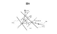
図5により、本発明の原理を説明する。図5(a)と(b)は、図1に示した本実施例による光ヘッドの光源からフォーカスレンズに至る光路図で、半導体ミラー5や複合素子12を省略した光路図である。(a)は本発明による二重ミラー11がある場合で、(b)は二重ミラー11がない場合を示す。半導体レーザチップの幅は通常250μm程度なので、半導体レーザチップ4aと4bの発光点間隔Dは、例えば300μmである。また、コリメートレンズ10の焦点距離fcは、例えば20mmである。図5(b)のようにコリメートレンズ10の光軸上に半導体レーザチップ4aを配置した場合、半導体レーザチップ4aから出射したレーザビーム6aは、フォーカスレンズ13に真っ直ぐに入射するので、収差が生じにくい。一方、半導体レーザチップ4bから出射したレーザビーム6bは、フォーカスレンズ13に角度θ=arctan(D/fc)=0.86°で斜め入射するため、収差(特にコマ収差)が生じ易い。そこで本実施例では、図5(a)に示す二重ミラー11を用いる。二重ミラー11は、波長660nmのレーザビーム6aは反射し波長780nmのレーザビーム6bは透過する反射面51aと、波長780nmのレーザビーム6bを反射する反射面51bとからなる。反射面51aは、例えば誘電体薄膜を積層したダイクロイックミラーで、入射するレーザビーム6aに対して45°に配置されている。一方、反射面51bは、例えばアルミニュウム膜のミラーで、反射面51a と角度αをなす。
【0023】
図6に示すように、反射面51aと反射面51b間の媒質のレーザビーム6bに対する屈折率をnとして、レーザビーム6bが反射面51aに入射する場合の屈折角γはsinγ=sin(π/4+θ)/nで、反射面51aを出射する場合の入射角γ‘はsinγ‘=sin(π/4)/nである。よって、レーザビーム6bの反射面51bにおける反射の法則によりγ−α=γ’+αを満たす角度、即ちα=(γ−γ’)/2が求まる。例えば、n=1.5でθ= 0.86°の場合は、α=0.23°である。レーザビーム6aに対して0.86°傾いたレーザビーム6bは、反射面51bが反射面51aに対して角度α=0.23°傾むいた二重ミラー11を用いることにより、レーザビーム6aと完全に平行になり、フォーカスレンズ13に真っ直ぐに入射し、収差を生じにくくすることができる。
【0024】
図13は、本発明を用いた光ディスク装置の構造を示し、(a)は上面図、(b)は側面図である。131は光ディスク装置の筐体である。132はモーターで、光ディスク装置の筐体131に取付けられていて、シャフト133を介して光ディスク15を回転させる。134は光ヘッドを示し、半導体基板1を収納したパッケージ41とフォーカスレンズ13が取り付いたレンズアクチュエータ135が取付けられている。136は光ヘッド134に取付けられたアクセス機構、137は光ディスク装置の筐体131に取付けられているレールである。光ヘッド134は、アクセス機構136によってレール137上をディスク15の半径方向に移動することができる。光ヘッド134の内部には、コリメートレンズ10と、二重ミラー11と複合素子12がある。パッケージ41に搭載されている半導体レーザチップ4aまたは4bから放射したレーザビーム66aまたは66bは、レンズアクチュエータ135のフォーカスレンズ13を介して光ヘッド134から放射され、回転する光ディスク15に照射される。反射ビームは、再度フォーカスレンズ13を介して光ヘッド134に入射し、一部はパッケージ41に搭載されている光検出素子7で受光され焦点ずれ検出信号が得られる。また、一部はパッケージ41に搭載されている光検出素子8で受光されトラックずれ検出信号と情報再生信号が得られる。
【0025】
本発明の第2実施例を、図7と図8を用いて説明する。図7は、図5のミラー11の替わりに本発明によるビーム整形プリズム71と72を用いた光ヘッドの光路図であり、図1に示した半導体ミラー5や複合素子12を省略した光路図である。半導体レーザチップ4aと4bの発光強度分布は、紙面に垂直な方向に広く、紙面内方向には狭い。10はコリメートレンズ、13はフォーカスレンズである。71と72は、レーザビーム6aと6bの紙面内方向のビーム幅を拡大し、等方的な光強度分布にするビーム整形プリズムである。73は、通常のミラーである。
【0026】
図8により、本発明の原理を説明する。プリズム71または72の屈折率をn、入射面81の入射角をi、屈折角をγとすれば、n*sinγ=sini。また、2本の光線82と83のプリズム入射前の間隔をh1、プリズム内部での間隔をh2とし、入射面81における光線82と83の入射点の間隔をlとすれば、h1=l*cosi、h2=l*cosγから、ビーム幅拡大率mは、m=cosγ/cosiである。プリズムの頂角βをβ=γとすれば、垂直出射のビーム整形プリズムとなる。入射角iの微小変異をΔi、屈折角γの微小変異をΔγとすれば、n*sin(γ+Δγ)=sin(i+Δi)より、n*Δγ=Δi/mとなる。また出射面84における垂直出射からの微小変異をΔjとすれば、出射面84での屈折の法則はΔj=n*Δγである。よって、Δj=Δi/mであり、ビーム幅拡大率mのプリズムを用いることにより、ビームの角度変異は1/mに低減することができる。
【0027】
例えば,半導体レーザレーザチップ4aと4bの発光強度分布が、紙面に垂直な方向で30度、紙面内方向で10度の場合、プリズム71と72を、屈折率n=1.5のガラスで頂角βをβ=36.14度の形状に製作し、各々のプリズムへの入射角iがi=62.2度になるように配置すれば、各々のプリズムによるビーム幅拡大率mはm=√3となり、2つのプリズム71と72の作用により出射ビームの光強度分布は等方的になる。また、半導体レーザチップ4aと4bの発光点間隔Dを300μmで、コリメートレンズ10の焦点距離fcを20mmとし、コリメートレンズ10の光軸上に半導体レーザチップ4aを配置した場合、半導体レーザチップ4bから出射したレーザビーム6bは、レーザビーム6aに比べて0.86°傾いてプリズム71に入射する。しかし、本発明によるビーム整形プリズム71と72の作用により、プリズム72を出射した後では、レーザビーム6bの傾きは0.29°となる。よって、レーザビーム4bがフォーカスレンズ13に入射する場合の傾きは、本発明のプリズムを用いることにより3分の1に低減でき、コマ収差等が生じにくくなる。
【0028】
本発明の第3実施例を、図9と図10を用いて説明する。図9は、図7のビーム整形プリズム71と72の替わりに本発明によるミラープリズム91を用いた光ヘッドの光路図であり、図1に示した半導体ミラー5や複合素子12を省略した光路図である。半導体レーザチップ4aと4bの発光強度分布は、紙面に垂直な方向に広く、紙面内方向には狭い。10はコリメートレンズ、13はフォーカスレンズである。ミラープリズム91は、レーザビーム6aと6bを屈折する屈折面92と反射する反射面93からなり、屈折面92と反射面93とのなす頂角はθである。反射面93には、アルミニウム等の反射膜が蒸着されている。ミラープリズム91は、レーザビーム6aと6bの紙面内方向のビーム幅を拡大し、等方的な光強度分布にするビーム整形作用と、入射ビームを垂直方向に反射する作用を有する。
【0029】
図10により、本発明の原理を説明する。レーザビーム101がミラープリズム91に入射する場合の入射角をi、屈折角をγ、レーザビーム101がミラープリズム91から出射する場合の入射角をγ’、出射角をi’、ミラープリズム91の屈折率をn、とすれば、屈折の法則により、n*sinγ=sini、n*sinγ’=sini’、である。また、反射面93は屈折面92に対してθ傾いているので、γ−θ=γ’+θである。レーザビーム101を入射方向とは直角方向に出射する条件は、i+i’=π/2である。以上の式から、θ=1/2*{arcsin(1/n*sini)−arcsin(1/n*cosi)}となる。さらに、入射時のビーム幅倍率m1は、m1=cosγ/cosi、出射時のビーム幅倍率m2は、m2=cosi’/cosγ’であるから、ミラープリズム91のビーム幅倍率Mは、M=m1*m2=cosγ/cosi*cosi’/cosγ’である。また、入射角iの微小変異をΔi、屈折角γの微小変異をΔγ、入射角γ’の微小変異をΔγ’、出射角i’の微小変異をΔi’とすれば、n*sin(γ+Δγ)=sin(i+Δi)、n*sin(γ’+Δγ’)=sin(i’+Δi’)、(γ+Δγ)−θ=(γ’+Δγ’)+θ、である。以上の微小変異を含んだ式から、Δi’=cosγ/cosi*cosi’/cosγ’*Δiが求まり、
Δi’=Δi/Mとなる。即ち、ビーム幅拡大率Mのミラープリズム91を用いることにより、ビームの角度変異は1/Mに低減することができる。
【0030】
例えば,半導体レーザレーザチップ4aと4bの発光強度分布が、紙面に垂直な方向で30度、紙面内方向で10度の場合、ミラープリズム91を、屈折率n=1.5のガラスで頂角θをθ=15.29度の形状に製作し、ミラープリズム91への入射角iがi=75.5度になるように配置すれば、ミラープリズム91によるビーム幅拡大率MはM=3となり、出射ビームの光強度分布は等方的になる。また、半導体レーザチップ4aと4bの発光点間隔Dを300μmで、コリメートレンズ10の焦点距離fcを20mmとし、コリメートレンズ10の光軸上に半導体レーザチップ4aを配置した場合、半導体レーザチップ4bから出射したレーザビーム6bは、レーザビーム6aに比べて0.86°傾いてミラープリズム91に入射する。しかし、本発明によるミラープリズム91の作用により、ミラープリズム91を出射した後では、レーザビーム6bの傾きは0.29°となる。よって、レーザビーム4bがフォーカスレンズ13に入射する場合の傾きは、本発明のプリズムを用いることにより3分の1に低減でき、コマ収差等が生じにくくなる。
【0031】
本発明の第4実施例を、図11を用いて説明する。111と112は、図7で説明したビーム整形プリズム71と72と同様に、紙面内方向のビーム幅を拡大する作用を有するビーム整形プリズムである。図7で説明した第2実施例では、ビーム整形プリズム71と72を出射したレーザビーム6bは、レーザビーム6aに対して0.29°傾いているので、フォーカスレンズ13でレーザビーム6bを収束させると、僅かながらコマ収差等が生じる可能性がある。本実施例では、僅かに残ったレーザビーム6bの傾きを取り除くために、図5で説明した二重ミラー11と同様に、レーザビーム6aを反射する反射面114aとレーザビーム6bを反射する反射面114bとからなる二重ミラー113を用いて、2つのレーザビームを同一方向に反射することができる。
【0032】
CD−R等のディスクを記録または再生する場合、ディスクに収束させる光スポットの形状は丸型よりも楕円型の方が都合のよい場合がある。本実施例では、ビーム整形プリズム111と112によるビーム幅拡大率は任意に設定できるので、丸型に限らず楕円型のスポットも形成でき、しかも、2つのレーザビームをフォーカスレンズ13に真っ直ぐに入射させることができる。
【0033】
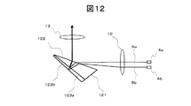
本発明の第5実施例を、図12を用いて説明する。121は二重ミラープリズムで、図9で説明したミラープリズム91と同様に、屈折面122による屈折により紙面内方向のビーム幅を拡大する作用を有する。図9で説明した第3実施例では、ミラープリズム91を出射したレーザビーム6bは、レーザビーム6aに対して0.29°傾いているので、フォーカスレンズ13でレーザビーム6bを収束させると、僅かながらコマ収差等が生じる可能性がある。本実施例の二重ミラープリズム121は、図5で説明した二重ミラー11と同様にレーザビーム6aを反射する反射面123aとレーザビーム6bを反射する反射面123bを有し、反射面123bを反射面123aに対して傾斜させることにより、僅かに残ったレーザビーム6bの傾きを取り除くことができ、2つのレーザビームを同一方向に反射することができる。
【0034】
本実施例においても、二重ミラープリズム121によるビーム幅拡大率は任意に設定できるので、丸型に限らず楕円型のスポットも形成でき、しかも、2つのレーザビームをフォーカスレンズ13に真っ直ぐに入射させることができる。
【0035】
【発明の効果】
以上述べたように、本発明によれば、複数のレーザ光源を用いて光学的情報媒体に情報を記録しまたは情報を再生するための光ヘッドにおいて、新たに高価な光学部品を用いることなく、光軸外に配置された半導体レーザからのレーザビームであってもフォーカスレンズにほぼ真っ直ぐ入射させることができ収差が生じにくい光ヘッド及びそれを用いた光学的情報媒体記録再生装置を実現することができる。
【図面の簡単な説明】
【図1】 本発明による光ディスク装置および光ヘッドの構成図
【図2】 図1における複合素子の回折格子部分の作用を説明する図
【図3】 図1における半導体基板の構成図
【図4】 図1におけるパッケージの構成図
【図5】 第1実施例における本発明の光ヘッドの主要構成図
【図6】 第1実施例における本発明の原理を説明する図
【図7】 第2実施例における本発明の光ヘッドの主要構成図
【図8】 第2実施例における本発明の原理を説明する図
【図9】 第3実施例における本発明の光ヘッドの主要構成図
【図10】 第3実施例における本発明の原理を説明する図
【図11】 第4実施例における本発明の光ヘッドの主要構成図
【図12】 第5実施例における本発明の光ヘッドの主要構成図
【図13】 本発明の光ヘッドを用いた光ディスク装置の構造図
【符号の説明】
1 … 半導体基板
4a … 半導体レーザチップ
4b … 半導体レーザチップ
10 … コリメートレンズ
13 … フォーカスレンズ
11,113 … 二重ミラー
71, 72 … ビーム整形プリズム
91 … ミラープリズム
121 … 二重ミラープリズム[0001]
BACKGROUND OF THE INVENTION
The present invention relates to an optical head for recording or reproducing information on an optical information medium such as an optical disk, and more particularly to an optical head using a laser module on which a plurality of semiconductor laser chips are mounted and an optical head using the same. The present invention relates to a typical information medium recording / reproducing apparatus.
[0002]
[Prior art]
Optical information recording / reproducing apparatuses such as optical disk apparatuses are desired to have various functions as well as to be reduced in size and thickness.
[0003]
For example, both CD-R (Compact Disk-Recordable), which is popular as a writable optical disc, and DVD (Digital Versatile Disc / Digital Video Disc), which has been developed as a higher-density writable optical disc in recent years, are the same. There is a significant demand for recording and reproducing with a small optical head. The laser wavelength suitable for CD-R recording / reproduction is about 780 nm, while the laser wavelength suitable for DVD recording / reproduction is about 660 nm. Therefore, both the laser light source having a wavelength of about 780 nm and the laser light source having a wavelength of about 660 nm are the same. It is necessary to mount on the optical head. Therefore, for example, in Japanese Patent Laid-Open Nos. 10-261240 and 10-289468, a CD semiconductor laser chip having a wavelength of about 780 nm, a semiconductor laser chip for DVD having a wavelength of about 660 nm, and a photodetecting element are combined into one unit. A small optical head has been proposed.
[0004]
Normally, beams with different emission point positions pass through different positions of the lens system at different angles, so even in these optical heads, the beams emitted from the two semiconductor laser chips are incident at different angles on the focus lens. To do. In the embodiments shown in Japanese Patent Application Laid-Open Nos. 10-261240 and 10-289468, a DVD semiconductor laser chip having a wavelength of 660 nm is formed of a focus lens and a collimating lens from the viewpoint of high-density recording and reproduction. The CD semiconductor laser chip having a wavelength of 780 nm is disposed outside the optical axis of the lens system. For this reason, since the DVD laser beam is incident directly on the focus lens, aberrations are unlikely to occur in the DVD laser spot. On the other hand, the CD laser beam is incident obliquely on the focus lens. Aberrations (especially coma) are likely to occur.
[0005]
Therefore, in Japanese Patent Laid-Open No. 10-261240, a holographic optical element 25 (25 is a number in the specification of Japanese Patent Laid-Open No. 10-261240) is used, and in Japanese Patent Laid-Open No. 10-289468, a polarizing prism (birefringence) is used. Plate) or hologram combining means 30 (30 is the number in the specification of Japanese Patent Application Laid-Open No. 10-289468), and only the optical path of the laser beam for CD is bent and directly incident on the focus lens.
[0006]
[Problems to be solved by the invention]
However, in the above-described conventional example, a DVD laser beam with a wavelength of 660 nm has no effect, and there is a special holographic optical element or a polarizing prism (birefringent plate) that bends only the optical path of a CD laser beam with a wavelength of 780 nm. This is necessary, and there is a problem that the cost of optical components of the optical head increases.
[0007]
On the other hand, thinning of the optical head is an important requirement, and in order to achieve thinning of the optical head, the examples of the above-mentioned Japanese Patent Application Laid-Open Nos. 10-261240 and 10-289468 are shown. Although not done, usually, an optical component other than the focus lens is arranged on a plane parallel to the disk surface, and a rising mirror is required to guide the beam to the focus lens. In addition, in order to record information, a beam shaping prism is needed to efficiently focus the laser beam with an anisotropic light intensity distribution emitted by the semiconductor laser onto a light spot with an isotropic light intensity distribution. It is. Therefore, in order to realize a low-cost optical head, it is necessary to reduce the number of optical components and reduce the cost of each optical component.
[0008]
An object of the present invention is an optical head for recording or reproducing information on an optical information medium using a plurality of laser light sources, and is disposed off the optical axis without using a new expensive optical component. Another object of the present invention is to provide an optical head in which an aberration hardly occurs when a laser beam from a semiconductor laser is incident almost straight on a focus lens, and an optical information medium recording / reproducing apparatus using the optical head.
[0009]
[Means for Solving the Problems]
In order to achieve the above object, in the first invention, a plurality of laser light sources having different wavelengths, a mirror that reflects a plurality of laser beams emitted from the laser light source, and a plurality of laser beams reflected by the mirror are optical disks or the like. In an optical head comprising an optical focusing means such as a focus lens for focusing as a light spot on the optical information medium, the mirror is composed of a plurality of reflecting surfaces that reflect laser beams of different wavelengths and is incident from different directions. The plurality of reflecting surfaces are not parallel to each other so that the plurality of laser beams are reflected in substantially the same direction.
[0010]
In the second invention, the mirror is arranged as a rising mirror for guiding the laser beam to the optical focusing means.
[0011]
In the third invention, a plurality of semiconductor laser chips, a collimating lens for converting a plurality of laser beams emitted from the semiconductor laser chip into parallel light beams, and a plurality of laser beams as optical spots on an optical information medium such as an optical disk An optical head comprising an optical focusing means such as a focusing lens for focusing, and a beam shaping prism for expanding the width of the laser beam in a direction in which a plurality of semiconductor laser chips are arranged between the collimating lens and the optical focusing means. Arranged.
[0012]
In the fourth invention, the beam shaping prism has a reflecting surface and is arranged as a rising mirror for guiding the laser beam to the optical focusing means.
[0013]
In the fifth aspect of the invention, a plurality of semiconductor laser chips having different wavelengths, a collimator lens that converts a plurality of laser beams emitted from the semiconductor laser chip into parallel light beams, a mirror that reflects the plurality of laser beams, and a reflection by the mirror In an optical head comprising a plurality of laser beams focused on an optical information medium such as an optical disc as a light spot, and a focusing lens and other optical focusing means, the width of the laser beam is aligned in a direction in which a plurality of semiconductor laser chips are arranged A beam-shaping prism that expands to a distance between the collimating lens and the mirror, and the mirror is composed of a plurality of reflecting surfaces that reflect laser beams of different wavelengths, and a plurality of laser beams incident from different directions are almost in the same direction. So that the reflective surfaces are not parallel to each other. It was.
[0014]
In the sixth invention, the beam shaping prism is disposed as a rising mirror for guiding the laser beam to the optical focusing means.
[0015]
DETAILED DESCRIPTION OF THE INVENTION
A first embodiment of the present invention will be described below with reference to FIGS. 1 to 6 and FIG.
[0016]
FIG. 1 shows a basic configuration of an optical disc apparatus and an optical head using the present invention.
[0017]
In this embodiment, the
[0018]
FIG. 3A shows the surface of the
[0019]
The photodetection element for obtaining the track deviation detection signal and the information reproduction signal indicated by 8 in FIG. 1 is composed of 38a and 38b in detail. Reference numeral 38a denotes four photodetecting elements that receive the laser beam 32a, and 38b denotes four photodetecting elements that receive the laser beam 32b. Output signals of the photodetecting elements 38a and 38b are input to an amplifier 39 formed on the semiconductor substrate. Is done. When the
[0020]
FIG. 3B shows a cross-sectional structure of the
[0021]
4A shows the structure of the
[0022]
The principle of the present invention will be described with reference to FIG. FIGS. 5A and 5B are optical path diagrams from the light source of the optical head according to the present embodiment shown in FIG. 1 to the focus lens, in which the
[0023]
As shown in FIG. 6, assuming that the refractive index of the medium between the reflecting
[0024]
FIG. 13 shows the structure of an optical disc apparatus using the present invention, where (a) is a top view and (b) is a side view.
[0025]
A second embodiment of the present invention will be described with reference to FIGS. FIG. 7 is an optical path diagram of an optical head using the
[0026]
The principle of the present invention will be described with reference to FIG. If the refractive index of the
[0027]
For example, when the emission intensity distributions of the semiconductor
[0028]
A third embodiment of the present invention will be described with reference to FIGS. FIG. 9 is an optical path diagram of an optical head using the
[0029]
The principle of the present invention will be described with reference to FIG. The incident angle when the
Δi ′ = Δi / M. That is, by using the
[0030]
For example, when the emission intensity distributions of the semiconductor
[0031]
A fourth embodiment of the present invention will be described with reference to FIG. Similarly to the
[0032]
When recording or reproducing a disc such as a CD-R, an elliptical shape may be more convenient for the shape of the light spot converged on the disc than a round shape. In the present embodiment, since the beam width enlargement ratio by the
[0033]
A fifth embodiment of the present invention will be described with reference to FIG.
[0034]
Also in this embodiment, since the beam width expansion ratio by the
[0035]
【The invention's effect】
As described above, according to the present invention, an optical head for recording or reproducing information on an optical information medium using a plurality of laser light sources can be used without newly using expensive optical components. It is possible to realize an optical head in which even a laser beam from a semiconductor laser arranged off the optical axis can be incident almost straight on a focus lens and hardly cause aberrations, and an optical information medium recording / reproducing apparatus using the optical head. it can.
[Brief description of the drawings]
FIG. 1 is a configuration diagram of an optical disk device and an optical head according to the present invention.
FIG. 2 is a diagram for explaining the operation of the diffraction grating portion of the composite element in FIG.
FIG. 3 is a configuration diagram of the semiconductor substrate in FIG.
4 is a block diagram of the package in FIG.
FIG. 5 is a main configuration diagram of the optical head of the present invention in the first embodiment.
FIG. 6 is a diagram for explaining the principle of the present invention in the first embodiment.
FIG. 7 is a main configuration diagram of an optical head of the present invention in a second embodiment.
FIG. 8 is a diagram for explaining the principle of the present invention in the second embodiment.
FIG. 9 is a main configuration diagram of an optical head of the present invention in a third embodiment.
FIG. 10 is a diagram for explaining the principle of the present invention in the third embodiment.
FIG. 11 is a main configuration diagram of an optical head of the present invention in a fourth embodiment.
FIG. 12 is a main configuration diagram of an optical head of the present invention in a fifth embodiment.
FIG. 13 is a structural diagram of an optical disk apparatus using the optical head of the present invention.
[Explanation of symbols]
1 ... Semiconductor substrate
4a: Semiconductor laser chip
4b ... Semiconductor laser chip
10 ... Collimating lens
13… Focus lens
11, 113 ... Double mirror
71, 72 ... Beam shaping prism
91… Mirror prism
121… Double mirror prism
Claims (10)
前記複数のレーザ光源から出射される複数のレーザ光束を平行光束に変換するコリメートレンズと、
前記複数の平行光束を反射するミラーと、
前記ミラーで反射された前記複数の平行光束を光学的情報媒体に光スポットとして集束する光学的集束手段とを有する光ヘッドであって、
前記ミラーは互いに非平行な複数の反射面を有し、前記ミラーに異なる方向から入射する前記複数の平行光束を、前記ミラーから略同一の方向に出射することを特徴とする光ヘッド。A plurality of laser light sources having different wavelengths;
A collimating lens that converts a plurality of laser beams emitted from the plurality of laser light sources into a parallel beam;
A mirror that reflects the plurality of parallel light fluxes;
An optical head having optical focusing means for focusing the plurality of parallel light beams reflected by the mirror as optical spots on an optical information medium,
2. The optical head according to claim 1, wherein the mirror has a plurality of non-parallel reflecting surfaces, and the plurality of parallel light beams incident on the mirror from different directions are emitted from the mirror in substantially the same direction.
前記複数のレーザ光源から出射される複数のレーザ光束を平行光束に変換するコリメートレンズと、
前記複数の平行光束を変化させるビーム整形手段と、
前記複数の平行光束を反射するミラーと、
前記ミラーで反射された前記複数の平行光束を光学的情報媒体に光スポットとして集束する光学的集束手段とを有する光ヘッドであって、
前記ビーム整形手段は、前記ビーム整形手段に異なる方向から入射する前記複数の平行光束の互いになす角度を小さくして前記ビーム整形手段から出射させることを特徴とする光ヘッド。A plurality of laser light sources having different wavelengths;
A collimating lens that converts a plurality of laser beams emitted from the plurality of laser light sources into a parallel beam;
Beam shaping means for changing the plurality of parallel light fluxes;
A mirror that reflects the plurality of parallel light fluxes;
An optical head having optical focusing means for focusing the plurality of parallel light beams reflected by the mirror as optical spots on an optical information medium,
The optical head characterized in that the beam shaping means emits the beam shaping means with a smaller angle formed by the plurality of parallel light beams incident on the beam shaping means from different directions.
前記ビーム整形手段と前記ミラーが一体部品であることを特徴とする光ヘッド。The optical head according to claim 2,
An optical head characterized in that the beam shaping means and the mirror are integral parts.
前記複数のレーザ光源から出射される複数のレーザ光束を平行光束に変換するコリメートレンズと、
前記複数の平行光束を変化させるビーム整形手段と、
前記複数の平行光束を反射するミラーと、
前記ミラーで反射された前記複数の平行光束を光学的情報媒体に光スポットとして集束する光学的集束手段とを有する光ヘッドであって、
前記ビーム整形手段は、前記ビーム整形手段に異なる方向から入射する前記複数の平行光束の互いになす角度を小さくして前記ビーム整形手段から前記ミラーへ出射させ、
前記ミラーは互いに非平行な複数の反射面を有し、前記ミラーに異なる方向から入射する前記複数の平行光束を、前記ミラーから略同一の方向に出射することを特徴とする光ヘッド。A plurality of laser light sources having different wavelengths;
A collimating lens that converts a plurality of laser beams emitted from the plurality of laser light sources into a parallel beam;
Beam shaping means for changing the plurality of parallel light fluxes;
A mirror that reflects the plurality of parallel light fluxes;
An optical head having optical focusing means for focusing the plurality of parallel light beams reflected by the mirror as optical spots on an optical information medium,
The beam shaping unit reduces the angle formed by the parallel light beams incident on the beam shaping unit from different directions and emits the beam from the beam shaping unit to the mirror,
2. The optical head according to claim 1, wherein the mirror has a plurality of non-parallel reflecting surfaces, and the plurality of parallel light beams incident on the mirror from different directions are emitted from the mirror in substantially the same direction.
前記ビーム整形手段と前記ミラーが一体部品であることを特徴とする光ヘッド。The optical head according to claim 4, wherein
An optical head characterized in that the beam shaping means and the mirror are integral parts.
前記ミラーは、前記複数の平行光束のうち少なくとも一の平行光束を反射させ、他の平行光束のうち少なくとも一の平行光束を屈折させる面を有することを特徴とする光ヘッド。In the optical head according to any one of claims 1, 4, and 5,
2. The optical head according to claim 1, wherein the mirror has a surface that reflects at least one of the plurality of parallel beams and refracts at least one of the other parallel beams.
前記ビーム整形手段は、前記複数の平行光束のいずれの強度分布も同じ方向に変化させ、その方向は前記複数のレーザ光源の配列方向と略同一であることを特徴とする光ヘッド。The optical head according to any one of claims 2 to 6,
The beam shaping means changes the intensity distribution of any of the plurality of parallel light beams in the same direction, and the direction is substantially the same as the arrangement direction of the plurality of laser light sources.
前記ミラーは、前記光学的集束手段に前記複数の平行光束を導くための立ち上げミラーとして配置されていることを特徴とする光ヘッド。In the optical head according to any one of claims 1 to 7,
The optical head is characterized in that the mirror is arranged as a rising mirror for guiding the plurality of parallel light beams to the optical focusing means.
前記複数のレーザ光源は同一の基板上に近接して配置され、
前記複数のレーザ光束の出射方向は略同一方向でかつ略平行であることを特徴とする光ヘッド。In the optical head according to any one of claims 1 to 8,
The plurality of laser light sources are arranged close to each other on the same substrate,
An optical head characterized in that emission directions of the plurality of laser light beams are substantially the same and substantially parallel.
少なくとも一の光ヘッドを搭載したことを特徴とする光学的情報記録再生装置。Among the optical heads according to any one of claims 1 to 9,
An optical information recording / reproducing apparatus comprising at least one optical head.
Priority Applications (3)
| Application Number | Priority Date | Filing Date | Title |
|---|---|---|---|
| JP30196699A JP3659089B2 (en) | 1999-10-25 | 1999-10-25 | Optical head and optical information medium recording / reproducing apparatus using the same |
| US09/517,594 US7106681B1 (en) | 1999-10-25 | 2000-03-03 | Optical head arrangements with single substrate lasers |
| US10/628,364 US20040022141A1 (en) | 1999-10-25 | 2003-07-29 | Optical head and optical information media recording/reproduction apparatus using the same |
Applications Claiming Priority (1)
| Application Number | Priority Date | Filing Date | Title |
|---|---|---|---|
| JP30196699A JP3659089B2 (en) | 1999-10-25 | 1999-10-25 | Optical head and optical information medium recording / reproducing apparatus using the same |
Publications (3)
| Publication Number | Publication Date |
|---|---|
| JP2001126297A JP2001126297A (en) | 2001-05-11 |
| JP2001126297A5 JP2001126297A5 (en) | 2005-02-24 |
| JP3659089B2 true JP3659089B2 (en) | 2005-06-15 |
Family
ID=17903281
Family Applications (1)
| Application Number | Title | Priority Date | Filing Date |
|---|---|---|---|
| JP30196699A Expired - Fee Related JP3659089B2 (en) | 1999-10-25 | 1999-10-25 | Optical head and optical information medium recording / reproducing apparatus using the same |
Country Status (2)
| Country | Link |
|---|---|
| US (2) | US7106681B1 (en) |
| JP (1) | JP3659089B2 (en) |
Families Citing this family (10)
| Publication number | Priority date | Publication date | Assignee | Title |
|---|---|---|---|---|
| JP2002074719A (en) * | 2000-08-24 | 2002-03-15 | Fujitsu Ltd | Optical apparatus |
| JP4151313B2 (en) | 2002-06-03 | 2008-09-17 | 株式会社日立製作所 | Optical regenerator |
| US20050180482A1 (en) * | 2004-01-23 | 2005-08-18 | Osowski Mark L. | Very low cost surface emitting laser diode arrays |
| JP4093213B2 (en) * | 2004-07-29 | 2008-06-04 | 松下電器産業株式会社 | Semiconductor laser device and optical pickup device using the same |
| JP4215703B2 (en) * | 2004-11-04 | 2009-01-28 | パナソニック株式会社 | Optical device and manufacturing method thereof |
| JP2008130128A (en) * | 2006-11-17 | 2008-06-05 | Funai Electric Co Ltd | Optical pickup device |
| JP2008140483A (en) * | 2006-12-04 | 2008-06-19 | Funai Electric Co Ltd | Optical pickup device |
| JP2008140484A (en) * | 2006-12-04 | 2008-06-19 | Funai Electric Co Ltd | Optical pickup device |
| JP2008275878A (en) * | 2007-04-27 | 2008-11-13 | Fuji Xerox Co Ltd | Hologram recording or reproducing optical device, and method for controlling hologram recording or reproducing optical device |
| KR20180002932U (en) | 2017-04-04 | 2018-10-12 | 박동현 | A life-saving neck band |
Family Cites Families (49)
| Publication number | Priority date | Publication date | Assignee | Title |
|---|---|---|---|---|
| US4520472A (en) * | 1983-02-07 | 1985-05-28 | Rca Corporation | Beam expansion and relay optics for laser diode array |
| EP0228620B1 (en) | 1985-12-10 | 1991-06-05 | Nec Corporation | Optical head comprising a diffraction grating for directing two or more diffracted beams to optical detectors |
| JPS6383931A (en) * | 1986-09-27 | 1988-04-14 | Toshiba Corp | Light emitting element |
| US5289313A (en) * | 1988-09-28 | 1994-02-22 | Canon Kabushiki Kaisha | Optical head using semiconductor laser array as light source |
| US5144614A (en) * | 1988-10-29 | 1992-09-01 | Sony Corporation | Optical pickup device |
| JPH02265028A (en) * | 1989-04-06 | 1990-10-29 | Mitsubishi Electric Corp | Optical recording and reproducing device |
| US5568315A (en) * | 1991-05-28 | 1996-10-22 | Discovision Associates | Optical beamsplitter |
| JPH05210868A (en) * | 1992-01-30 | 1993-08-20 | Hitachi Ltd | Multibeam separation type optical head |
| CA2088701C (en) * | 1992-02-05 | 1998-01-27 | Yoshio Yoshida | Optical information reproducing apparatus |
| DE69319676T2 (en) * | 1992-08-07 | 1998-12-10 | Matsushita Electric Ind Co Ltd | Optical system and device for image information |
| US5513164A (en) * | 1992-09-11 | 1996-04-30 | Kabushiki Kaisha Toshiba | Optical recording and reproducing apparatus |
| US5694385A (en) * | 1993-09-24 | 1997-12-02 | Ricoh Comany, Ltd. | Optical pickup apparatus |
| JP3167066B2 (en) * | 1993-10-06 | 2001-05-14 | キヤノン株式会社 | Optical recording / reproducing device |
| US5579291A (en) * | 1993-12-24 | 1996-11-26 | Sony Corporation | Compact-size magneto-optical head apparatus |
| JPH07182687A (en) * | 1993-12-24 | 1995-07-21 | Sharp Corp | Optical pick-up |
| JP3541416B2 (en) * | 1994-03-08 | 2004-07-14 | ソニー株式会社 | Optical device |
| JPH07326065A (en) * | 1994-05-27 | 1995-12-12 | Hitachi Ltd | Optical information processor |
| US5687152A (en) | 1994-10-25 | 1997-11-11 | Kabushiki Kaisha Sankyo Seiki Seisakusho | Optical pickup system |
| US6118752A (en) * | 1995-07-07 | 2000-09-12 | Matsushita Electric Industrial Co., Ltd. | Optical information recording medium offset pre-pit array indicating identification information |
| JPH09128772A (en) * | 1995-11-01 | 1997-05-16 | Sony Corp | Optical pickup |
| US5737296A (en) | 1996-01-23 | 1998-04-07 | Matsushita Electric Industrial Co., Ltd. | Focus and tracking error detection by using plus and minus first order diffracted light |
| EP0831472B1 (en) * | 1996-03-11 | 2003-09-03 | Seiko Epson Corporation | Optical pickup and optical recording apparatus |
| KR100207682B1 (en) * | 1996-05-29 | 1999-07-15 | 윤종용 | Laser astigmatism compensating method of optical pickup device |
| US6081496A (en) * | 1996-12-26 | 2000-06-27 | Kabushiki Kaisha Toshiba | Objective lens and optical disk driving apparatus using the same |
| JPH10283652A (en) | 1997-02-24 | 1998-10-23 | Hoetron Inc | Optical head using two semiconductor laser having different wavelengths |
| JPH10241199A (en) * | 1997-02-25 | 1998-09-11 | Sharp Corp | Optical pickup |
| JPH10261241A (en) | 1997-03-19 | 1998-09-29 | Sony Corp | Recording/reproducing device and method thereof |
| JP3653923B2 (en) * | 1997-03-19 | 2005-06-02 | ソニー株式会社 | Recording / reproducing apparatus and method |
| JP3638194B2 (en) * | 1997-03-19 | 2005-04-13 | パイオニア株式会社 | Optical pickup device |
| JPH10289468A (en) | 1997-04-10 | 1998-10-27 | Konica Corp | Optical pickup device and light source unit for the device |
| JP3545905B2 (en) | 1997-04-30 | 2004-07-21 | 株式会社リコー | Polarization separation element and optical head using the polarization separation element |
| KR100253810B1 (en) * | 1997-07-10 | 2000-04-15 | 구자홍 | Optical source module with two kinds of wavelengths and optical pickup device thereof |
| JPH11110786A (en) | 1997-10-01 | 1999-04-23 | Matsushita Electric Ind Co Ltd | Optical pickup |
| TW336311B (en) | 1997-10-15 | 1998-07-11 | Ind Tech Res Inst | Method and device for focusing and tracking of an optical head |
| EP0911818A1 (en) * | 1997-10-27 | 1999-04-28 | Deutsche Thomson-Brandt Gmbh | Compact dual wavelength optical pickup head |
| KR100266223B1 (en) * | 1998-01-16 | 2000-09-15 | 구자홍 | Optical pickup apparatus |
| JP3407679B2 (en) * | 1998-03-24 | 2003-05-19 | 日本電気株式会社 | Optical head and optical head manufacturing apparatus |
| JP2000011417A (en) | 1998-06-26 | 2000-01-14 | Toshiba Corp | Semiconductor laser array and its production, optical integrated unit, optical pickup as well as optical disk drive assembly |
| US6043935A (en) * | 1998-07-17 | 2000-03-28 | Hoetron, Inc. | Wavelength sensitive beam combiner with aberration correction |
| KR100295102B1 (en) * | 1998-07-29 | 2001-07-12 | 이형도 | Optical pickup |
| EP0987769B1 (en) * | 1998-09-18 | 2003-05-02 | Sumitomo Electric Industries, Ltd. | Photodiode module |
| TW411454B (en) * | 1998-10-28 | 2000-11-11 | Ind Tech Res Inst | Optical read/write head for dual wavelength |
| US6434105B1 (en) * | 1998-12-25 | 2002-08-13 | Olympus Optical Co., Ltd. | Optical pickup device |
| US6385355B1 (en) * | 1999-03-15 | 2002-05-07 | Fuji Xerox Co., Ltd. | Optical deflection element |
| TW419653B (en) * | 1999-03-16 | 2001-01-21 | Ind Tech Res Inst | Optical pick-up head with multiple light sources |
| JP2000268391A (en) * | 1999-03-16 | 2000-09-29 | Minebea Co Ltd | Optical pickup device |
| JP4038375B2 (en) | 1999-08-04 | 2008-01-23 | 株式会社日立製作所 | Laser module, optical head using the same, and optical information recording / reproducing apparatus |
| US6614825B1 (en) | 1999-10-05 | 2003-09-02 | Zhijiang Hang | Monolithic VCSEL-based optical pickup and servo control device |
| JP2001184705A (en) * | 1999-12-27 | 2001-07-06 | Hitachi Ltd | Optical head and optical information recorder using the same |
-
1999
- 1999-10-25 JP JP30196699A patent/JP3659089B2/en not_active Expired - Fee Related
-
2000
- 2000-03-03 US US09/517,594 patent/US7106681B1/en not_active Expired - Fee Related
-
2003
- 2003-07-29 US US10/628,364 patent/US20040022141A1/en not_active Abandoned
Also Published As
| Publication number | Publication date |
|---|---|
| US7106681B1 (en) | 2006-09-12 |
| JP2001126297A (en) | 2001-05-11 |
| US20040022141A1 (en) | 2004-02-05 |
Similar Documents
| Publication | Publication Date | Title |
|---|---|---|
| US7672202B2 (en) | Optical pickup apparatus | |
| JP3304053B2 (en) | Optical head and optical disk device | |
| JP3659089B2 (en) | Optical head and optical information medium recording / reproducing apparatus using the same | |
| JPH11296893A (en) | Optical pickup | |
| KR100253810B1 (en) | Optical source module with two kinds of wavelengths and optical pickup device thereof | |
| JP2000030288A (en) | Optical pickup element | |
| EP0860819A2 (en) | Optical pickup using two semiconductor lasers with different wavelengths | |
| EP0911818A1 (en) | Compact dual wavelength optical pickup head | |
| JP2000076688A (en) | Multi-wavelength optical pickup device | |
| TW442784B (en) | Laser module and optical head | |
| JP2002279683A (en) | Optical pickup device | |
| JP2881734B2 (en) | Annular shutter mirror, method of manufacturing the same, and optical pickup device for heterogeneous optical disks using the same | |
| US6947367B2 (en) | Single means for converting beam widths of plural laser beams with different entry and exit angle with offset | |
| JP2001143297A (en) | 3-laser module and optical head or optical information medium recorder-reproducer using the module | |
| JP3987259B2 (en) | Optical pickup device | |
| JP4389287B2 (en) | Optical head device | |
| JP3607836B2 (en) | Optical pickup device | |
| JP3694943B2 (en) | Optical apparatus and optical pickup | |
| JP2904419B2 (en) | Magneto-optical pickup | |
| JP2001043555A (en) | Optical pickup device | |
| JP2002237087A (en) | Optical pickup device | |
| JP2506972B2 (en) | Optical pickup device | |
| JP3965857B2 (en) | Optical head and optical information medium recording / reproducing apparatus using the same | |
| JP2002304761A (en) | Optical pickup device | |
| EP0996120A1 (en) | Optical pickup compatible with a digital versatile disk and a recordable compact disk using a holographic ring lens |
Legal Events
| Date | Code | Title | Description |
|---|---|---|---|
| A521 | Written amendment |
Free format text: JAPANESE INTERMEDIATE CODE: A523 Effective date: 20040317 |
|
| A621 | Written request for application examination |
Free format text: JAPANESE INTERMEDIATE CODE: A621 Effective date: 20040317 |
|
| A977 | Report on retrieval |
Free format text: JAPANESE INTERMEDIATE CODE: A971007 Effective date: 20041109 |
|
| A131 | Notification of reasons for refusal |
Free format text: JAPANESE INTERMEDIATE CODE: A131 Effective date: 20041116 |
|
| A521 | Written amendment |
Free format text: JAPANESE INTERMEDIATE CODE: A523 Effective date: 20050117 |
|
| TRDD | Decision of grant or rejection written | ||
| A01 | Written decision to grant a patent or to grant a registration (utility model) |
Free format text: JAPANESE INTERMEDIATE CODE: A01 Effective date: 20050222 |
|
| A61 | First payment of annual fees (during grant procedure) |
Free format text: JAPANESE INTERMEDIATE CODE: A61 Effective date: 20050307 |
|
| FPAY | Renewal fee payment (event date is renewal date of database) |
Free format text: PAYMENT UNTIL: 20090325 Year of fee payment: 4 |
|
| FPAY | Renewal fee payment (event date is renewal date of database) |
Free format text: PAYMENT UNTIL: 20090325 Year of fee payment: 4 |
|
| FPAY | Renewal fee payment (event date is renewal date of database) |
Free format text: PAYMENT UNTIL: 20100325 Year of fee payment: 5 |
|
| FPAY | Renewal fee payment (event date is renewal date of database) |
Free format text: PAYMENT UNTIL: 20110325 Year of fee payment: 6 |
|
| FPAY | Renewal fee payment (event date is renewal date of database) |
Free format text: PAYMENT UNTIL: 20110325 Year of fee payment: 6 |
|
| LAPS | Cancellation because of no payment of annual fees |