JP3649635B2 - Active matrix display device - Google Patents
Active matrix display device Download PDFInfo
- Publication number
- JP3649635B2 JP3649635B2 JP2000034516A JP2000034516A JP3649635B2 JP 3649635 B2 JP3649635 B2 JP 3649635B2 JP 2000034516 A JP2000034516 A JP 2000034516A JP 2000034516 A JP2000034516 A JP 2000034516A JP 3649635 B2 JP3649635 B2 JP 3649635B2
- Authority
- JP
- Japan
- Prior art keywords
- common
- electrode
- pixel
- pixel electrode
- line
- Prior art date
- Legal status (The legal status is an assumption and is not a legal conclusion. Google has not performed a legal analysis and makes no representation as to the accuracy of the status listed.)
- Expired - Lifetime
Links
Images


Landscapes
- Liquid Crystal (AREA)
- Devices For Indicating Variable Information By Combining Individual Elements (AREA)
- Thin Film Transistor (AREA)
Description
【0001】
【発明の属する技術分野】
本明細書で開示する発明は、アクティブマトリクス型の表示装置に関するものである。特に、表示装置の素子基板の配線・電極構造に関するものである。
【0002】
【従来の技術】
従来より一対の基板間に液晶を挟んで保持し、この液晶にそれぞれの基板の表面に配置された一対の電極から電界を印加し、液晶の光学特性を変化させることによって、表示を行う構成が知られている。
【0003】
この従来より用いられている構成は、電界を基板に対して垂直に加えることにより、液晶分子を基板と平行な方向に配したり、基板に垂直な方向に配したりすることを基本的な動作とする。このような動作を行わせることにより、液晶の電気光学的な特性を変化させて、表示を行っている。
【0004】
しかし、液晶分子を基板に垂直な方向に配するということは、表示に際して、液晶の光学異方性の影響が大きく表れてしまうことになる。
【0005】
例えば、基板に垂直な方向から表示を見た場合と、垂直方向から少しずれた方向から表示を見た場合を考える。この場合、後者の視点からの表示は、液晶分子の長軸に対して少し傾いた視点からのものとなる。このことは、前者の視点からのものと比較して光学特性が大きく変化してしまうことを意味する。
【0006】
この現象の具体的な例としては、ディスプレイを少し斜めから見ると表示が不鮮明になったり、暗くなったりする場合の例を挙げることができる。
【0007】
一般にこの問題は視野角の問題として知られている。即ち、液晶ディスプレイの視野角がブラウン管やエレクトロルミネセンス型(EL型)の表示装置に比較して狭いという問題として知られている。
【0008】
このような問題を解決する構成として、特公昭63−21907号公報に記載された構成が知られている。
【0009】
この構成においては、液晶分子が基板に平行な方向において回転することにより、その光学特性を変化させる。従って、液晶分子が基板に対して垂直になることがなく、前述の視野角の問題を解決することができる。
【0010】
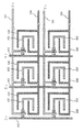
図21にこのような基板に平行な方向に液晶分子が回転するような動作を実現するための画素の従来例の構成を示す。
【0011】
図21に示す構成において、ゲイト線11、ソース線12は格子状に配置されている。ゲイト線11は薄膜トランジスタ13のゲイト電極に信号を与えるための信号線であり、またソース線12は薄膜トランジスタ13のソースに画像データの信号を供給するための信号線である。
【0012】
薄膜トランジスタ13のドレインに接続された画素電極14は、櫛型の形状を有し、他方の櫛型の電極15と噛み合うように配置されている。
【0013】
他方の櫛形電極15は所定の電位に保たれた配線16から延在している。
【0014】
このような構成とすると、櫛型に形成された一対の電極14と15間において、基板の表面に平行な方向に電界が形成され、それによって液晶分子が基板に平行な方向に回転するような動作を行わすことができる。
【0015】
しかし、図21に示す構成においては、17で示される領域において、ソース線12と画素電極14の一部とが隣合う構成となっている。更に、18で示される領域においても、ゲイト線11と画素電極14の一部とが隣合う構成となっている。これは、画素電極14が、ソース線12及びゲイト線11との間での相互干渉を受け易い状態であり、不正確な画像が表示されてしまう原因となる。
【0016】
図21に示す構成は、櫛形の電極15を配線16によって列毎に接続したものである。これに対して、図22に示す構成は、櫛形の電極を所定の電位を有する配線を行毎に接続したものである。しかしながら、図22に示すような配置を採用した場合でも、電極間の相互干渉の問題は存在する。
【0017】
図22に示す構成においては、ゲイト線21、ソース線22は格子状に配置され、ゲイト線21は薄膜トランジスタ23のゲイト電極に信号を与えるための信号線であり、またソース線22は薄膜トランジスタ23のソースに画像データの信号を供給するための信号線である。また、薄膜トランジスタ23のドレインには、画素電極24が接続されている。
【0018】
また、櫛形の電極25は、所定の電位を有する配線26から延在した電極であり、画素電極24と互いに噛み合うような櫛型に形成されている。これら2つの電極24と25間において基板に平行な方向に電界が形成される。
【0019】
図22に示す構成においても27で示される領域において、画素を構成する電極24とソース線22との相互干渉を受け易い状態となる。更に、28で示す領域においても、画素電極24とゲイト線21との間で相互干渉を受け易い状態となっている。
【0020】
【発明が解決しようとする課題】
本明細書で開示する発明は、液晶ディスプレイが有する視野角の狭さの問題を解決した構成を提供することを課題とする。また、基板に平行な方向に電界を印加することにより表示を行う構成における問題を解消し、鮮明な画像を表示することができる構成を提供することを課題とする。
【0021】
【課題を解決するための手段】
上述の問題点を解決するために本発明に係る表示装置の構成は、
アクティブマトリクス型の液晶表示装置であって、
基板上に格子状に配置されたゲイト線及びソース線と、
各画素に配置され、前記ゲイト線に接続されたゲイトと、前記ソース線に接続されたソースとを有する薄膜トランジスタと、
該薄膜トランジスタのドレインに接続された第1の電極と、
所定の電位に保たれたコモン線と、
該コモン線から延在する第2の電極とを有し、
前記第1の電極と前記第2の電極とは互いに噛み合うような渦巻形状に配置されていることを特徴とする表示装置。
【0022】
更に、本発明に係る表示装置の他の構成は、
アクティブマトリクス型の液晶表示装置であって、
基板上に格子状に配置されたゲイト線及びソース線と、
各画素に配置され、前記ゲイト線に接続されたゲイトと、前記ソース線に接続されたソースとを有する薄膜トランジスタと、
該薄膜トランジスタのドレインに接続された第1の電極と、
所定の電位に保たれたコモン線と、
前記コモン線に接続された第2の電極と、
を有し、
前記第1の電極と前記第2の電極とは、互いの内部に入り込むように配置されていることを特徴とする表示装置。
【0023】
更に本発明に係る表示装置の他の構成は、
アクティブマトリクス型の液晶表示装置の画素において、
基板上に形成された薄膜トランジスタのドレインに接続された第1の電極と、該第1の電極との間において前記基板面に平行な成分を有する電界を発生させるための第2の電極と、
を有し、
前記第1の電極と前記第2の電極それぞれは渦巻状の形状を有し、前記基板面内において互いに噛み合う状態で配置されていることを特徴とする表示装置。
【0024】
更に、本発明に係る表示装置の他の構成は、
アクティブマトリクス型の液晶表示装置の画素において、
同一基板上に渦巻状に噛み合った一対の電極が形成されており、
前記一対の電極間に基板に概略平行な成分を有した電界が形成される構成を有することを特徴とする表示装置。
【0025】
【発明の実施の形態】
本明細書で開示する発明に係る表示装置は、同一基板上に画素電極と対向基板とを配置するようにしたものであり、本発明の実施形態の一例を図1を用いて説明する。
【0026】
図1には、アクティブマトリクス型の液晶表示装置であって、
基板上に格子状に配置されたゲイト線101及びソース線102と、
各画素に配置され、前記ゲイト線101に接続されたゲイトと、前記ソース線102に接続されたソースとを有する薄膜トランジスタ100と、
該薄膜トランジスタ100のドレインに接続された第1の電極103と、
所定の電位に保たれたコモン線104と、
該コモン線104から延在する第2の電極105とを有する表示装置を示す。
【0027】
図1において、前記第1の電極103と前記第2の電極105とは互いに噛み合うような渦巻形状に配置されている。
【0028】
或いは、前記第1の電極103と前記第2の電極105とは、互いの内部に入り込むように配置されている。
【0029】
図1に示す構成においては、基板に平行な方向に主な電界の成分を形成するために第1の電極103および第2の電極105は同一平面上に形成されていることが好ましい。なお、必ずしも、第1の電極103と第2の電極105は同一層内に存在していなくともよく、第1の電極103と第2の電極104とは絶縁膜を隔てて、異なる層内に存在してもよい。
【0030】
本発明においては、第1の電極と第2の電極を同一基板内に形成すると同時に薄膜トランジスタに接続された第1の電極が、ソース線又はゲイト線のうち少なともの一方の信号線がつくる電界に干渉されないようにするのが好ましい。
【0031】
従って、第1の電極が電界に干渉されないようにするために、本発明では、前記基板面内において前記第1の電極と前記ソース線の間隙、又は前記第1の電極と前記ゲイト線の間隙のうち、少なくともいずれか一方の間隙に配置されている領域を前記第2の電極が有する構成とすることが好ましい。
【0032】
上記の構成の実施形態の1つとして、図1に示すように、前記基板面内において、前記第2の電極105が、前記第1の電極103と前記ソース線102の間隙、および前記第1の電極103と前記ゲイト線101の間隙双方に配置されている領域を有する構成をとりうる。
【0033】
或いは、図12に示すように、前記基板面内において、前記第2の電極342は、前記第1の電極341と前記ソース線102の間隙だけに配置されている領域を少なくとも有する構成をとりうる。
【0034】
また、図12に示すように、前記基板面内において、前記第2の電極352は、前記第1の電極351と前記ゲイト線101の間隙だけに配置されている領域を少なくとも有する構成をとりうる。
【0035】
【実施例】
〔実施例1〕
図1は本実施例のアクティブマトリックス型の液晶表示装置の1単位の画素部の概略の上面図であり、図2は図1における線A−A’による概略の断面図である。
【0036】
図2に示すように、素子基板200において、ガラス又は石英等の基板201上には、薄膜トランジスタ100のシリコン膜から成る活性層202、ゲイト絶縁膜203が順次に積層され、酸化珪素膜等からなるゲイト絶縁膜203上に、薄膜トランジスタ101のゲイトに接続されたゲイト線101(スキャン線ともいう)が形成される。 更に、酸化珪素膜等の第1の層間絶縁膜204が形成され、活性層202のソース/ドレインのコンタクトホールが形成されて、ソースと接続されるソース線(ソース線ともいう)102が形成される。次に、第2の層間絶縁膜205が形成され、活性層202のドレインのコンタクトホールが形成されて、第2の層間絶縁膜205上にドレインに接続された矩形渦巻状の画素電極103と、コモン線104、コモン線104から延在する矩形渦巻状のコモン電極105が形成される。更に、その表面に樹脂等からなる保護膜206、配向膜207が順次に形成される。
【0037】
更に、素子基板200と対向される対向基板210において、ガラス又は石英等の基板211の表面に配向膜212が配置される。素子基板200と対向基板210は配向膜207、212側を内側にして、図示しないシール材により貼り合わされて、これらの基板200、210の間隙に液晶材料213が封入されている。
【0038】
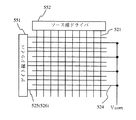
また、図3は図1に示す電極・配線をマトリクス状に際の構成図であり、図4は素子基板のブロック構成図である。
図4に示すように、ゲイト線101とソース線102はマトリックス状に配置され、ゲイト線101はゲイト線ドライバ401に接続され、ソース線102はソース線ドライバ402に接続されている。
【0039】
また、コモン電極105は行毎にコモン線104に接続されている。コモン線104は所定の電位Vcom に固定されているため、全てのコモン電極105は等しい電位Vcom に固定される。なお、電位Vcom は例えば接地電位とすればよい。
【0040】
更に、図1に示すように、コモン線104から延在した矩形渦巻状のコモン電極105に対して、薄膜トランジスタ100のドレインに接続され画素電極103は噛み合うように、かつ電極間距離をX軸方向、Y軸方向とも一定にされて配置されている。
【0041】
図1に示す構成においては、一対の画素電極103とコモン電極105が対向された画素が構成される。表示の際には、これらの2つの電極103と104間に電界が生じて、当該画素領域上に存在する液晶材料213に電界が印加されて、表示が行われる。
【0042】
図2に示すように、画素電極103とコモン電極105は同一平面内に構成されているので、この電界は基板201の表面に概略平行な方向に主な成分を有し、この電界によって、液晶分子は基板201に平行な方向に力を受ける。従って、電極103と104間の電界を制御することにより、液晶分子の配向を制御することができ、この液晶分子の配向が変化し、その電気光学特性が変化するため、表示を行うことができる。
【0043】
図1に示す構成においては、薄膜トランジスタ100のドレインに接続された画素電極103はコモン電極105によって囲まれ、かつゲイト線101及びソース線102から隔てられている状態となっている。
【0044】
従って、コモン電極103を所定の電位に固定することによって、画素電極103がゲイト線101とソース線102からの影響を受けることを抑制することができるので、画素の周囲において滲みのない鮮明で、正確な画像を表示することができる。
【0045】
更に、図1に示す構成では、一つの画素において、その中心付近に向かって渦巻状に一対の電極103、105が互いに噛み合うように延在しているので、電極の端部において形成される周辺からの干渉による影響が出にくいという特徴を有する。
【0046】
これは、それぞれの電極103、105の端部が画素の中心部に存在することによる。画素の中心部においては、上記のような周辺からの干渉による影響が小さなものとなるからである。
【0047】
本実施例では、画素電極103と、コモン電極105とが重ならないので、図2に示すように同一の層内に形成するようにしたが、絶縁物によりこ画素電極103と、コモン電極105とを上下間で分離してもよい。この場合には、画素電極103とコモン電極105の上下の順序は問わないが、電極103、105間で基板に平行な電界の強度を液晶分子の配向を制御することが可能な値とすることが必要になる。
【0048】
また、図3、4に示すように、本実施例では、コモン線104によってコモン電極105を行毎に接続したが、列毎にコモン電極105を接続してもよい。
この場合の、アクティブマトリクス型液晶表示装置のブロック図を図5に示す。図5において、図4と同一の符号は同一の部材を示す。
【0049】
〔実施例2〕
本実施例は実施例1の改良例であり、画素電極の渦巻きの巻き数を増加したものである。図6は、本実施例のアクティブマトリックス型の液晶表示装置の1単位の画素部の概略の上面図であり、図1と同一の符号は同一の部材を示す。
【0050】
図6においては、図1の画素電極103よりも、画素電極301の電極の巻数を増加している。これに対応して、コモン電極302の巻き数も増加され、コモン電極302によって、画素電極301を取り囲んで、画素電極301がゲイト線101とソース線102とに隣接しないようにしたものである。
【0051】
〔実施例3〕
実施例1では、図1に示すように、画素電極103とコモン電極105間での電界は紙面内において、2つのX軸方向の線分、Y軸方向の成分を有することになるため、液晶分子の配向方向が一様でない。このため、一般的に使用されている直線偏光軸を有する偏光板を使用することが困難であるので、場所毎に偏向軸が異なるような特別な偏光板が必要となる。更に、このような偏光板は位置合わせに困難を伴う。
【0052】
本実施例は実施例1の変形例であり、上記の問題点を解消して、一様な直線偏光軸を有する一般的な偏光板を使用するできるようにしたものである。
【0053】
図7は本実施例の画素部の概略の上面図であり、図8は図7における線B−B’による概略の断面図である。なお、図7、8において、図1、2と同一の符号は同一の部材を示す。
【0054】
本実施例は、実施例1の画素電極103、コモン電極105の配置を基板面内で変形したものである。
実施例1では、画素電極103とコモン電極105をX軸、Y軸両方向に等間隔に配置したが、本実施例では、画素電極311とコモン電極312の電極間隔を部分的にX軸方向の間隔を縮小するようにしている。
なお、他の部材の構成は実施例と同様である。
【0055】
画素電極311とコモン電極312間の電界は殆ど基板の表面に平行であるが、このようにX軸方向の電極間隔を縮小させることで、この電界のX軸方向の成分を小さくして、主にY成分のみに電界を有するようにすることができる。従って、液晶材料213に基板面に平行に電界を印加することができると同時に、液晶分子の配向の方向を一様にすることができるので、一様な直線偏光軸を有する一般的な偏光板の使用が可能になる。
更に、電極間隔を縮小することによって、画素部の開口率が向上されると共に、基板間隔が縮小された電極は画素に並列に接続された補助容量として機能させることができるという効果も生ずる。
【0056】
この補助容量の容量は、画素電極311とコモン電極312が近接している部分の長さで決定することができるので、画素電極301、コモン電極302の巻数を制御することによって、この補助容量の容量を制御することができる。
【0057】
例えば、図6に示す画素において、画素電極301とコモン電極302とのX軸方向の間隔を縮小することで、画素電極301とコモン電極302が近接している部分をより長くできるので、より大きな補助容量を付加することができる。
【0058】
〔実施例4〕
本実施例は実施例3の変形例であり、画素部の開口率を向上するようにしたものである。図9は本実施例のアクティブマトリックス型の液晶表示装置の1単位の画素部の概略の上面図であり、図10は図9における線C−C’による概略の断面図である。なお、図9、10において、図1、2と同一の符号は同一の部材を示す。
【0059】
実施例3では、同一平面内で画素電極311とコモン電極312のX軸方向の間隔を縮小したが、本実施例では、図9に示すように、画素電極322とコモン電極323のX軸方向の間隔を更に縮小して、電極321、322の矩形渦巻きの一辺を重ねるようにしたものである。
【0060】
このため、画素電極311とコモン電極312が上下間でショートしないように、図10に示すように、第3の層間絶縁膜230によって画素電極321とコモン電極322とを上下方向で分離している。なお、画素電極321とコモン電極322との上下の位置関係を入れ換えてもよい。
【0061】
本実施例も、実施例2と同様に、X軸方向の電極321と322間の距離を縮小させることにより、これらの電極321と322間に発生する電界の成分を、基板面に平行で、かつ殆どX成分のない、Y成分を主とすることができる。このため、液晶材料213に基板面に平行に電界を印加することが可能であり、かつ液晶分子の回転軸の方向を一様にすることができるので、一様な直線偏光軸を有するような一般的な偏光板を使用することができる。
【0062】
更に、電極321と322はその重なる部分でより大きな補助容量として機能させることができる。また、画素電極321とコモン電極322を間隔を更に縮小して、重ねるようにしため、画素部の開口率をより向上することができる。
【0063】
〔実施例5〕
図11に本実施例の概略の構成を示す。本実施例に示す構成は、薄膜トランジスタ100のドレインに接続された画素電極331と、コモン線104から延在するコモン電極331とを曲線形状にしたことを特徴とする。
なお、図11において、図1と同一の符号は、同一の部材を示し、電極331、332以外は、実施例1と同様の構成を有する。従って図4に示すように、ゲイト線101、ソース線102、コモン線104は、格子状に配置されている。
【0064】
図11に示すような構成とすると、電極331、332のパターンが直角に曲がるような形状が存在しないので、電極間に均一な電界を形成することができる。
【0065】
〔実施例6〕
上述した実施例1〜5においては、画素電極をゲイト線、ソース線双方に隣接しないように、コモン電極を画素電極とソース線との間隙、及び画素電極とゲイト線との間隙とに配置される形状としたが、以下に示す実施例では、画素電極がソース線又はゲイト線の何れか一方の信号線と隣接しないように、コモン電極を画素電極とソース線又はゲイト線何れか一方との間隙に配置される形状としたものである。
【0066】
この場合には、画素電極はゲイト線又はソース線いずれか一方の電位の影響を被ることになるが、コモン電極の占有面積を縮小することができるため、表示に有効な領域の面積が大きくなるという利点が生ずる。
【0067】
本実施例はコモン電極を画素電極とソース線との間隙に配置されるようにしたものであり、図12は本実施例の画素領域の概略の上面図であり、図1と同一の符号は同一の部材を示す。
【0068】
ゲイト線101とソース線102が、薄膜トランジスタ100に接続されて格子状に配置されている。薄膜トランジスタ100のドレインには、矩形渦巻状の画素電極341が接続されている。更に、所定の電位に固定されたコモン線104から延在したコモン電極342は、画素電極341と同様な矩形渦巻状に形成されている。
【0069】
図12に示す構成においては、一対の電極341と342によって画素が構成されている。この2つの電極が組となって、当該画素領域上に存在する液晶に対して基板に平行な方向を有する電界(主に基板に平行な方向を有する)を印加する構成となっている。
【0070】
この構成においては、ソース線102が所定の電位に固定されたコモン線104から延在したコモン電極342によって囲まれた状態となって、画素電極341がソース線102と隣接しないようにしている。コモン線104の電位は適当な電位に設定すればよく、たとえば接地電位とすることができる。
【0071】
上記の構成では、画素電極341がソース線102の電位の影響を受けることを抑制することができるので、画素の周囲において滲みのない鮮明な画像を表示することができる。
【0072】
本実施例においては、薄膜トランジスタ100のドレインに接続された画素電極341に対して、互いの渦巻形状が噛み合うように同じ平面内にコモン線104から延在したコモン電極342が配置される。そして、これら一対の電極341と342の間隔は概略等間隔とされ、これらの電極341、342間において電界が形成される。
【0073】
この電界は、基板に概略平行な方向に主な成分を有する電界であり、この電界によって液晶分子は、基板に平行な方向に力を受ける。そしてこの電界強度を制御することにより、液晶分子はこの電界に従い回転する。
【0074】
そしてこの液晶分子の回転によって、液晶の電気光学特性が変化し、表示を行うことができる。
【0075】
図12に示す方式は、一つの画素において、その中心付近に向かって渦巻状に一対の電極341、342が互いに噛み合うように延在しているので、電極の端部は周辺部との干渉による影響が出にくいという特徴を有する。
【0076】
これは、それぞれの電極の端部が画素の中心部に存在することによる。画素の中心部においては、周辺部との干渉による影響が小さなものとなる。
【0077】
なお、図12に示す画素の配置状態をマトリクス状に形成したアクティブマトリス型の液晶表示装置の配線の状態を図5に示す。
【0078】
〔実施例7〕
本実施例はコモン電極を画素電極とゲイト線との間隙に配置されるようにしたものであり、図13は本実施例の画素領域の概略の上面図であり、図1と同一の符号は同一の部材を示す。
【0079】
ゲイト線101とソース線102が、薄膜トランジスタ100に接続されて格子状に配置されている。薄膜トランジスタ100のドレインには、矩形渦巻状の画素電極351が接続されている。更に、所定の電位に固定されたコモン線104から延在したコモン電極352は、画素電極351と同様な矩形渦巻状に形成されている。
【0080】
図13に示す構成においては、基板面内で概略等間隔に対峙された一対の電極351と352によって画素が構成されている。この2つの電極が組となって、当該画素領域上に存在する液晶に対して基板に平行な方向を有する電界(主に基板に平行な方向を有する)を印加する構成となっている。
なお、本実施例の素子基板の構成は図4に示す構成となる。
【0081】
この構成においては、ゲイト線101が所定の電位に固定されたコモン線104から延在したコモン電極352によって囲まれた状態となって、画素電極341がソース線102と隣接しないようにしている。コモン線104の電位は適当な電位に設定すればよく、たとえば接地電位とすることができる。
【0082】
上記の構成では、画素電極341がソース線102の電位の影響を受けることを抑制することができるので、画素の周囲において滲みのない鮮明な画像を表示することができる。
【0083】
〔実施例8〕
本実施例は、実施例6に示す構成に比較してコモン線の配線数を少なくすることができる構成に関する。図14は本実施例の概略の上面図であり、図16は本実施例の素子基板の構成図である。
【0084】
図14には、2つの画素領域の概要が示されている。図14に示す構成においては、2つの画素のそれぞれに薄膜トランジスタ507と508が配置されている。薄膜トランジスタ507、508において、それぞれのゲイトには同一行のゲイト線501が接続され、ソースはソース線505、506にそれぞれ接続されている。更に、ドレインには矩形渦巻状の画素電極502、503がそれぞれ接続されている。 なお、図16において、551はゲイト線ドライバであり、552はソース線ドライバである。
【0085】
図14に示す構成においては、504で示されるコモン線が隣接した2つの列毎に共通なものとなっている。コモン線504からコモン電極509と510が延在し、それぞれ画素電極502と503に概略等間隔に対向して配置されている。このため、電極502と509間、電極503と510間に基板面に平行な電界が生じて、表示を行うことができる。
【0086】
本実施例の場合には、図14に示すように1本のコモン線504を隣接する2つの列で共有しているため、コモン線の本数はソース線の本数の1/2にすることができる。これは図5と図16を比較すれば明らかである。
【0087】
なお、本実施例では、画素電極502、503、コモン電極509、510の形状を実施例6と同様あるいは、鏡面対称な形状としたが、実施例1〜5に示す電極と同様な形状として、画素電極をゲイト線、ソース線とも隣接しないようにしてもよい。
【0088】
更に、図14において、画素電極502、503とゲイト線501との間隙にもコモン線からの延在部分を配置して、画素電極502、503がゲイト線501、ソース線505、506とも隣接しないようにすることもできる。
【0089】
〔実施例9〕
本実施例は、実施例7に示す構成に比較してコモン線の配線数を少なくすることができる構成に関する。図15は本実施例の概略の上面図であり、図17は本実施例の素子基板の構成図である。
【0090】
図15には、2つの画素領域の概要が示されている。図15に示す構成においては、2つの画素のそれぞれに薄膜トランジスタ527と528が配置されている。薄膜トランジスタ527、528において、それぞれのソースには同一行のソース線521が接続され、ゲイトにはソース線525、526がそれぞれ接続されている。更に、ドレインには矩形渦巻状の画素電極522、523がそれぞれ接続されている。
なお、図17において、551はゲイト線ドライバであり、552はソース線ドライバである。
【0091】
図15に示す構成においては、524で示されるコモン線が隣接した2つの行毎に共通なものとなっている。コモン線524からはコモン電極529と530が延在し、それぞれ画素電極522と523に概略等間隔に対向して配置されている。このため、電極522と529間、電極523と530間に基板面に平行な電界が生じて、表示を行うことができる。
【0092】
本実施例の場合には、図15に示すように1本のコモン線524を隣接する2つの行で共有しているため、コモン線の本数はソース線の本数の1/2にすることができる。これは図4と図17を比較すれば明らかである。
【0093】
〔実施例10〕
本実施例は、図18に示すようにゲイト線605と606、さらにソース線607と608とで囲まれる領域に配置された2つの画素601と602を1組として、1つの画素を構成することを特徴とする。
【0094】
これらの2つの画素は以下の4つの状態を表示することができる。即ち、601と602の画素が共にOFFの状態、601の画素がOFFで602の画素がONの状態、601の画素がONで602の画素がOFFの状態、601と602の画素が共にONの状態を選択することができる。
【0095】
このような組み合わせを行うことで、4階調の表示を行うことができる。
【0096】
なお図18において、603と604で示される領域は、601、602とは別の画素を構成する領域である。
【0097】
また図18に示す構成が特徴とするのは、コモン線609が2×2のマトリクス状に配置された4つの画素601と602と603と604とにおいて共通である。
更に、本実施例の場合には、4つの画素601〜604のコモン電極を列方向で1本のコモン線609で接続するようにしているため、コモン線609の本数は、ソース線の本数に対して1/2になる。このため、本実施例の場合も実施例8と同様に、素子基板の構成は図16のようになる。
【0098】
従って、図18に示す構成とすることで、画素の電極構成が複雑でも配線は簡略化したものとすることができる。
【0099】
〔実施例11〕
本実施例の概略の構成を図19に示す。図19に示すのは、ゲイト線701とソース線702と703、さらにコモン線704によって囲まれた領域に2つの画素領域を配置したことを特徴とする。
【0100】
図19において、薄膜トランジスタ707のドレインに接続された画素電極705と、コモン線704から延在したコモン電極709とは対向して配置され、一対の電極を構成する。これらの一対の電極により画素領域が構成され、これら一対の電極間において基板に平行な方向に電界が形成される。
【0101】
同様に、薄膜トランジスタ708のドレインに接続された画素電極706と、、コモン線704から延在したコモン電極710とは、互いに対になって一対の電極を成し、画素領域を構成している。一対の電極706と710間で基板面に平行な電界が形成される。
【0102】
本実施例では、それそれの画素領域において、画素電極705、706とソース線702、703とが隣接しないように、これらの電極間をコモン電極709、710によって隔てているため、ソース線の電位の影響を抑制することができるため、良好な表示を行うことができる。
【0103】
〔実施例12〕
図20に本実施例の構成を示す。図20に示す構成は、ゲイト線801、804と、ソース線802、803とで囲まれた領域に4つの画素領域が配置されている。
【0104】
これらの4つ薄膜トランジスタ806〜809のドレインには矩形渦巻状の画素電極810〜813がそれぞれ接続され、所定の電位に固定されたコモン線805から延在したコモン電極814〜817はそれぞれ画素電極810〜813に同一平面内で対向して配置されて、4つの画素を形成する。
【0105】
この4つの画素はそれぞれ独立に利用することもできる。また4つを1群として画素を構成し、面積階調表示を行わすこともできる。
【0106】
4つの画素電極810〜813はそれぞれコモン電極814〜817によって、ソース線802、803と隣接しないようにされているため、良好な表示を行うことができる。
【0107】
また、隣接する2つの行毎にコモン電極は1本のコモン線に接続されているため、コモン線の本数をゲイト線の本数が1/2になる。従って、本実施例の素子基板の構成は図17に示される。
【0108】
上記の実施例では、薄膜トランジスタをプレナー型としたが、スタガー型等の他構造の薄膜トランジスタを使用することも可能である。この場合には、薄膜トランジスタの電極・配線の接続構造にあわせて、ゲイト線、ソース線、コモン線、画素電極の積層順序を決定すればよく、コモン線と画素電極が重ならない限り、同一層内に配置することが可能である。
【0109】
また、上記の実施例では、液晶表示装置について説明したが、本発明は他の電気光学表示装置に応用することも可能である。例えば、エレクトロルミネセンス型(EL型)表示装置に応用することができる。この場合には、素子基板、対向基板の配向膜を省略し、液晶材料の代わりにEL材料を使用すればよい。本発明では、同一基板上に配置された対向電極によって基板の表面に平行な電界が発生するため、EL材料を均一に発光させることができる。
【0110】
【発明の効果】
本明細書で開示する発明に係る表示装置は、同一基板上に画素電極と対向基板とを配置するようにしたため以下のような効果を得る。
【0111】
他方の基板には配線を形成する必要が無くなるので、パネル作製工程が容易になり、また基板貼り合わせするための基板間隔のマージンが増大するため、基板の位置合わせが容易になる。
【0112】
更に、電極・配線を精度良く形成することが可能になり、電極間距離を正確にすることができるので、画素を高密度に形成することができる。
【0113】
更に、従来では、基板間で液晶材を誘電体とする負荷容量が発生しているが、本発明では、同一基板上に画素電極と対向基板とを配置するようにしたため、
このような負荷容量が生成することが無くなるため、動作速度が向上され、更に消費電力を削減することもできる。
【0114】
また、液晶ディスプレイが有する視野角の狭さの問題を解決した構成を提供することができる。
【0115】
更に、本発明では、基板に平行な方向に電界を印加することにより表示を行う構成における問題を解消したため、即ち、薄膜トランジスタのドレイン接続された画素電極(第1の電極)が、少なくともゲイト線又はソース線のいずれか一方と隣接しないようにして、更には、ゲイト線、ソース線双方とも隣接しないようにして、画素電極の電位の乱れを抑制したため、鮮明な画像を表示することができる構成を提供することができる。
【0116】
従って、本発明に係る表示装置は、例えば、高精細化が要求されるような空間光変調器として使用することができる。
【図面の簡単な説明】
【図1】 実施例1の画素領域の上面図である。
【図2】 図1の線A−A’における断面図である。
【図3】 実施例のアクティブマトリクスの配線構成を示す図。
【図4】 実施例1の素子基板のブロック構成図である。
【図5】 図4の変形例の素子基板のブロック構成図である。
【図6】 実施例2の画素領域の上面図である。
【図7】 実施例3の画素領域の上面図である。
【図8】 図7の線B−B’における断面図である。
【図9】 実施例4の画素領域の上面図である。
【図10】 図9の線C−C’における断面図である。
【図11】 実施例5の画素領域の上面図である。
【図12】 実施例6の画素領域の上面図である。
【図13】 実施例7の画素領域の上面図である。
【図14】 実施例8の画素領域の上面図である。
【図15】 実施例9の画素領域の上面図である。
【図16】 実施例8の素子基板のブロック構成図である。
【図17】 実施例9の素子基板のブロック構成図である。
【図18】 実施例10の画素領域の上面図である。
【図19】 実施例11の画素領域の上面図である。
【図20】 実施例12の画素領域の上面図である。
【図21】 従来例の画素領域の上面図である。
【図22】 他の従来例の画素領域の上面図である。
【符号の説明】
101 ゲイト線(ゲイト線)
103 画素電極
104 コモン線
105 コモン電極
102 ソース線(ソース線)
100 薄膜トランジスタ
200 素子基板
210 対向基板
601、602、603、604 画素
605、606 ゲイト線
607、608 ソース線
609 コモン線
701 ゲイト線
702、703 ソース線
704 コモン線
705、706 画素電極
707、708 薄膜トランジスタ
709、710 コモン電極
801、804 ゲイト線
802、803 ソース線
805 コモン線
806、807、808、809 薄膜トランジスタ
810、811、812、813 画素電極
814、815、816、817 コモン電極[0001]
BACKGROUND OF THE INVENTION
The invention disclosed in this specification relates to an active matrix display device. In particular, the present invention relates to a wiring / electrode structure of an element substrate of a display device.
[0002]
[Prior art]
Conventionally, the liquid crystal is held between a pair of substrates, and an electric field is applied to the liquid crystal from a pair of electrodes disposed on the surface of each substrate to change the optical characteristics of the liquid crystal, thereby performing display. Are known.
[0003]
This conventionally used configuration is basically arranged to arrange liquid crystal molecules in a direction parallel to the substrate or in a direction perpendicular to the substrate by applying an electric field perpendicular to the substrate. Let it be an action. By performing such an operation, display is performed by changing the electro-optical characteristics of the liquid crystal.
[0004]
However, arranging liquid crystal molecules in a direction perpendicular to the substrate greatly affects the optical anisotropy of the liquid crystal during display.
[0005]
For example, consider a case where the display is viewed from a direction perpendicular to the substrate and a case where the display is viewed from a direction slightly deviated from the vertical direction. In this case, the display from the latter viewpoint is from a viewpoint slightly inclined with respect to the long axis of the liquid crystal molecules. This means that the optical characteristics are greatly changed as compared with the former viewpoint.
[0006]
As a specific example of this phenomenon, there is an example in which the display becomes unclear or dark when the display is viewed from a slight angle.
[0007]
This problem is generally known as a viewing angle problem. That is, it is known as a problem that the viewing angle of a liquid crystal display is narrower than that of a cathode ray tube or an electroluminescence type (EL type) display device.
[0008]
As a configuration for solving such a problem, a configuration described in Japanese Patent Publication No. 63-21907 is known.
[0009]
In this configuration, the liquid crystal molecules rotate in a direction parallel to the substrate, thereby changing the optical characteristics. Therefore, the liquid crystal molecules are not perpendicular to the substrate, and the above-described viewing angle problem can be solved.
[0010]
FIG. 21 shows a configuration of a conventional example of a pixel for realizing such an operation that liquid crystal molecules rotate in a direction parallel to the substrate.
[0011]
In the configuration shown in FIG. 21, the
[0012]
The
[0013]
The other comb-
[0014]
With such a configuration, an electric field is formed between the pair of
[0015]
However, in the configuration shown in FIG. 21, the
[0016]
In the configuration shown in FIG. 21, comb-
[0017]
In the configuration shown in FIG. 22, the
[0018]
Further, the comb-
[0019]
In the configuration shown in FIG. 22 as well, in the region indicated by 27, it becomes easy to receive mutual interference between the
[0020]
[Problems to be solved by the invention]
An object of the invention disclosed in this specification is to provide a structure that solves the problem of narrow viewing angle of a liquid crystal display. It is another object of the present invention to provide a configuration capable of solving a problem in a configuration in which display is performed by applying an electric field in a direction parallel to the substrate and displaying a clear image.
[0021]
[Means for Solving the Problems]
In order to solve the above problems, the configuration of the display device according to the present invention is as follows.
An active matrix type liquid crystal display device,
Gate lines and source lines arranged in a grid on the substrate;
A thin film transistor disposed in each pixel and having a gate connected to the gate line and a source connected to the source line;
A first electrode connected to the drain of the thin film transistor;
A common line maintained at a predetermined potential;
A second electrode extending from the common line,
The display device, wherein the first electrode and the second electrode are arranged in a spiral shape so as to mesh with each other.
[0022]
Furthermore, another configuration of the display device according to the present invention is as follows.
An active matrix type liquid crystal display device,
Gate lines and source lines arranged in a grid on the substrate;
A thin film transistor disposed in each pixel and having a gate connected to the gate line and a source connected to the source line;
A first electrode connected to the drain of the thin film transistor;
A common line maintained at a predetermined potential;
A second electrode connected to the common line;
Have
The display device, wherein the first electrode and the second electrode are arranged so as to enter each other.
[0023]
Furthermore, another configuration of the display device according to the present invention is as follows.
In a pixel of an active matrix type liquid crystal display device,
A first electrode connected to a drain of a thin film transistor formed on a substrate; a second electrode for generating an electric field having a component parallel to the substrate surface between the first electrode;
Have
The display device, wherein each of the first electrode and the second electrode has a spiral shape and is arranged in a state of being engaged with each other in the substrate surface.
[0024]
Furthermore, another configuration of the display device according to the present invention is as follows.
In a pixel of an active matrix type liquid crystal display device,
A pair of electrodes that are spirally meshed on the same substrate are formed,
A display device having a structure in which an electric field having a component substantially parallel to a substrate is formed between the pair of electrodes.
[0025]
DETAILED DESCRIPTION OF THE INVENTION
A display device according to the invention disclosed in this specification is configured such that a pixel electrode and a counter substrate are arranged over the same substrate, and an example of an embodiment of the present invention will be described with reference to FIG.
[0026]
FIG. 1 shows an active matrix type liquid crystal display device,
A
A
A
A display device having a
[0027]
In FIG. 1, the
[0028]
Alternatively, the
[0029]
In the configuration shown in FIG. 1, the
[0030]
In the present invention, the first electrode and the second electrode are formed in the same substrate, and at the same time, the first electrode connected to the thin film transistor generates an electric field generated by at least one signal line of the source line and the gate line. It is preferable not to be interfered with.
[0031]
Therefore, in order to prevent the first electrode from being interfered by an electric field, in the present invention, the gap between the first electrode and the source line, or the gap between the first electrode and the gate line in the substrate surface. Of these, the second electrode preferably has a region disposed in at least one of the gaps.
[0032]
As one embodiment of the above configuration, as shown in FIG. 1, the
[0033]
Alternatively, as shown in FIG. 12, in the substrate surface, the
[0034]
In addition, as shown in FIG. 12, the
[0035]
【Example】
[Example 1]
FIG. 1 is a schematic top view of a pixel unit of one unit of the active matrix type liquid crystal display device of this embodiment, and FIG. 2 is a schematic cross-sectional view taken along line AA ′ in FIG.
[0036]
As shown in FIG. 2, in the
[0037]
Further, in the
[0038]
3 is a configuration diagram when the electrodes and wirings shown in FIG. 1 are arranged in a matrix, and FIG. 4 is a block configuration diagram of the element substrate.
As shown in FIG. 4, the
[0039]
The
[0040]
Further, as shown in FIG. 1, the rectangular spiral
[0041]
In the configuration shown in FIG. 1, a pixel in which a pair of
[0042]
As shown in FIG. 2, since the
[0043]
In the configuration illustrated in FIG. 1, the
[0044]
Therefore, by fixing the
[0045]
Further, in the configuration shown in FIG. 1, in one pixel, the pair of
[0046]
This is because the end portions of the
[0047]
In this embodiment, since the
[0048]
As shown in FIGS. 3 and 4, in this embodiment, the
A block diagram of the active matrix liquid crystal display device in this case is shown in FIG. In FIG. 5, the same reference numerals as those in FIG. 4 denote the same members.
[0049]
[Example 2]
The present embodiment is an improved example of the first embodiment, in which the number of spirals of the pixel electrode is increased. FIG. 6 is a schematic top view of a pixel unit of one unit of the active matrix type liquid crystal display device of this embodiment, and the same reference numerals as those in FIG. 1 denote the same members.
[0050]
In FIG. 6, the number of turns of the
[0051]
Example 3
In the first embodiment, as shown in FIG. 1, the electric field between the
[0052]
The present embodiment is a modification of the first embodiment, which solves the above-described problems and makes it possible to use a general polarizing plate having a uniform linear polarization axis.
[0053]
FIG. 7 is a schematic top view of the pixel portion of this embodiment, and FIG. 8 is a schematic cross-sectional view taken along line BB ′ in FIG. 7 and 8, the same reference numerals as those in FIGS. 1 and 2 denote the same members.
[0054]
In the present embodiment, the arrangement of the
In the first embodiment, the
In addition, the structure of other members is the same as that of an Example.
[0055]
The electric field between the
Further, by reducing the electrode interval, the aperture ratio of the pixel portion is improved, and the electrode having the reduced substrate interval can function as an auxiliary capacitor connected in parallel to the pixel.
[0056]
The capacity of the auxiliary capacitor can be determined by the length of the portion where the
[0057]
For example, in the pixel shown in FIG. 6, by reducing the distance between the
[0058]
Example 4
The present embodiment is a modification of the third embodiment and improves the aperture ratio of the pixel portion. FIG. 9 is a schematic top view of a pixel unit of one unit of the active matrix type liquid crystal display device of this embodiment, and FIG. 10 is a schematic cross-sectional view taken along line CC ′ in FIG. 9 and 10, the same reference numerals as those in FIGS. 1 and 2 denote the same members.
[0059]
In the third embodiment, the distance between the
[0060]
Therefore, the
[0061]
In the present embodiment, similarly to the second embodiment, by reducing the distance between the
[0062]
Furthermore, the
[0063]
Example 5
FIG. 11 shows a schematic configuration of the present embodiment. The structure shown in this embodiment is characterized in that the
In FIG. 11, the same reference numerals as those in FIG. 1 denote the same members, and the configuration other than the
[0064]
When the structure shown in FIG. 11 is used, there is no shape in which the patterns of the
[0065]
Example 6
In the first to fifth embodiments described above, the common electrode is disposed in the gap between the pixel electrode and the source line and the gap between the pixel electrode and the gate line so that the pixel electrode is not adjacent to both the gate line and the source line. However, in the embodiment shown below, the common electrode is connected to either the pixel electrode and the source line or the gate line so that the pixel electrode is not adjacent to the signal line of either the source line or the gate line. The shape is arranged in the gap.
[0066]
In this case, the pixel electrode is affected by the potential of either the gate line or the source line. However, since the area occupied by the common electrode can be reduced, the area of the effective area for display increases. The following advantages arise.
[0067]
In this embodiment, the common electrode is arranged in the gap between the pixel electrode and the source line. FIG. 12 is a schematic top view of the pixel area of this embodiment, and the same reference numerals as those in FIG. The same member is shown.
[0068]
[0069]
In the configuration shown in FIG. 12, a pair of
[0070]
In this configuration, the
[0071]
With the above structure, the
[0072]
In the present embodiment, the
[0073]
This electric field is an electric field having a main component in a direction substantially parallel to the substrate, and the liquid crystal molecules receive a force in a direction parallel to the substrate. By controlling the electric field strength, the liquid crystal molecules rotate according to the electric field.
[0074]
The rotation of the liquid crystal molecules changes the electro-optical characteristics of the liquid crystal, and display can be performed.
[0075]
In the method shown in FIG. 12, in one pixel, the pair of
[0076]
This is because the end of each electrode exists in the center of the pixel. In the central part of the pixel, the influence of interference with the peripheral part is small.
[0077]
Note that FIG. 5 shows a wiring state of an active matrix liquid crystal display device in which the pixel arrangement state shown in FIG. 12 is formed in a matrix.
[0078]
Example 7
In this embodiment, the common electrode is arranged in the gap between the pixel electrode and the gate line. FIG. 13 is a schematic top view of the pixel area of this embodiment, and the same reference numerals as those in FIG. The same member is shown.
[0079]
[0080]
In the configuration shown in FIG. 13, a pixel is constituted by a pair of
The configuration of the element substrate of this example is the configuration shown in FIG.
[0081]
In this configuration, the
[0082]
With the above structure, the
[0083]
Example 8
The present embodiment relates to a configuration that can reduce the number of common lines compared to the configuration shown in the sixth embodiment. FIG. 14 is a schematic top view of the present embodiment, and FIG. 16 is a configuration diagram of the element substrate of the present embodiment.
[0084]
FIG. 14 shows an outline of two pixel regions. In the configuration shown in FIG. 14,
[0085]
In the configuration shown in FIG. 14, the
[0086]
In the case of the present embodiment, as shown in FIG. 14, since one
[0087]
In this embodiment, the shape of the
[0088]
Further, in FIG. 14, extending portions from the common line are also arranged in the gaps between the
[0089]
Example 9
The present embodiment relates to a configuration that can reduce the number of common lines compared to the configuration shown in the seventh embodiment. FIG. 15 is a schematic top view of the present embodiment, and FIG. 17 is a configuration diagram of the element substrate of the present embodiment.
[0090]
FIG. 15 shows an outline of two pixel regions. In the configuration shown in FIG. 15,
In FIG. 17, 551 is a gate line driver and 552 is a source line driver.
[0091]
In the configuration shown in FIG. 15, the common line indicated by 524 is common to every two adjacent rows.
[0092]
In the case of the present embodiment, since one
[0093]
Example 10
In this embodiment, as shown in FIG. 18, two
[0094]
These two pixels can display the following four states. That is, both the
[0095]
By performing such a combination, display of four gradations can be performed.
[0096]
In FIG. 18, areas indicated by 603 and 604 are areas constituting pixels different from those of 601 and 602.
[0097]
Also, the configuration shown in FIG. 18 is common to the four
Further, in the case of this embodiment, the common electrodes of the four
[0098]
Therefore, with the configuration shown in FIG. 18, the wiring can be simplified even if the electrode configuration of the pixel is complicated.
[0099]
Example 11
A schematic configuration of the present embodiment is shown in FIG. FIG. 19 is characterized in that two pixel regions are arranged in a region surrounded by a
[0100]
In FIG. 19, the
[0101]
Similarly, the
[0102]
In this embodiment, the
[0103]
Example 12
FIG. 20 shows the configuration of this embodiment. In the configuration shown in FIG. 20, four pixel regions are arranged in a region surrounded by
[0104]
The rectangular
[0105]
These four pixels can also be used independently. In addition, a group of four pixels can be configured to perform area gradation display.
[0106]
Since the four
[0107]
Further, since the common electrode is connected to one common line every two adjacent rows, the number of common lines is halved from the number of common lines. Therefore, the configuration of the element substrate of this embodiment is shown in FIG.
[0108]
In the above embodiment, the thin film transistor is a planar type, but a thin film transistor having another structure such as a stagger type may be used. In this case, the stacking order of the gate line, source line, common line, and pixel electrode may be determined according to the connection structure of the electrode and wiring of the thin film transistor. As long as the common line and the pixel electrode do not overlap, It is possible to arrange in
[0109]
In the above embodiments, the liquid crystal display device has been described. However, the present invention can be applied to other electro-optical display devices. For example, the present invention can be applied to an electroluminescence type (EL type) display device. In this case, the alignment films on the element substrate and the counter substrate may be omitted, and an EL material may be used instead of the liquid crystal material. In the present invention, since the electric field parallel to the surface of the substrate is generated by the counter electrode disposed on the same substrate, the EL material can emit light uniformly.
[0110]
【The invention's effect】
The display device according to the invention disclosed in this specification has the following effects because the pixel electrode and the counter substrate are arranged on the same substrate.
[0111]
Since there is no need to form wiring on the other substrate, the panel manufacturing process is facilitated, and the margin of the substrate interval for bonding the substrates is increased, so that the alignment of the substrates is facilitated.
[0112]
Furthermore, it becomes possible to form electrodes / wirings with high accuracy, and the distance between electrodes can be made accurate, so that pixels can be formed with high density.
[0113]
Furthermore, in the past, load capacitance using a liquid crystal material as a dielectric material has occurred between the substrates, but in the present invention, since the pixel electrode and the counter substrate are arranged on the same substrate,
Since such load capacity is not generated, the operation speed is improved, and power consumption can be further reduced.
[0114]
In addition, it is possible to provide a configuration that solves the problem of narrow viewing angle of a liquid crystal display.
[0115]
Furthermore, in the present invention, the problem in the structure in which display is performed by applying an electric field in a direction parallel to the substrate is solved, that is, the pixel electrode (first electrode) connected to the drain of the thin film transistor is at least a gate line or Since the disturbance of the potential of the pixel electrode is suppressed so as not to be adjacent to any one of the source lines and further to be not adjacent to either the gate line or the source line, a clear image can be displayed. Can be provided.
[0116]
Therefore, the display device according to the present invention can be used, for example, as a spatial light modulator that requires high definition.
[Brief description of the drawings]
FIG. 1 is a top view of a pixel region in Example 1. FIG.
FIG. 2 is a cross-sectional view taken along line AA ′ of FIG.
FIG. 3 is a diagram illustrating a wiring configuration of an active matrix according to an embodiment.
4 is a block configuration diagram of an element substrate of Example 1. FIG.
FIG. 5 is a block configuration diagram of an element substrate according to a modification of FIG. 4;
FIG. 6 is a top view of a pixel region according to a second embodiment.
FIG. 7 is a top view of a pixel region in Example 3.
FIG. 8 is a cross-sectional view taken along line BB ′ of FIG.
FIG. 9 is a top view of a pixel region in Example 4.
10 is a cross-sectional view taken along line CC ′ of FIG.
FIG. 11 is a top view of a pixel region in Example 5.
12 is a top view of a pixel region according to Example 6. FIG.
FIG. 13 is a top view of a pixel region in Example 7.
FIG. 14 is a top view of a pixel region according to an eighth embodiment.
15 is a top view of a pixel region in Example 9. FIG.
16 is a block configuration diagram of an element substrate in Example 8. FIG.
17 is a block diagram of an element substrate in Example 9. FIG.
18 is a top view of a pixel region in Example 10. FIG.
19 is a top view of a pixel region in Example 11. FIG.
20 is a top view of a pixel region in Example 12. FIG.
FIG. 21 is a top view of a pixel region of a conventional example.
FIG. 22 is a top view of a pixel region of another conventional example.
[Explanation of symbols]
101 Gate line (Gate line)
103 pixel electrode
104 Common wire
105 Common electrode
102 Source line (source line)
100 Thin film transistor
200 element substrate
210 Counter substrate
601 602 603 604 pixels
605, 606 Gate line
607, 608 source line
609 Common wire
701 Gate line
702, 703 Source line
704 Common wire
705, 706 Pixel electrode
707, 708 Thin film transistor
709, 710 Common electrode
801, 804 Gate line
802, 803 source line
805 Common wire
806, 807, 808, 809 Thin film transistor
810, 811, 812, 813 Pixel electrode
814, 815, 816, 817 Common electrode
Claims (12)
同一基板側に、格子状に配置された複数のゲイト線及び複数のソース線と、複数のコモン線とが設けられ、前記画素ごとに薄膜トランジスタ、画素電極及びコモン電極が設けられ、前記画素電極と前記コモン電極間の電圧により液晶の配向を制御するアクティブマトリクス型表示装置であって、
前記複数の画素において、それぞれ、前記薄膜トランジスタのゲイト電極は前記ゲイト線に接続され、前記薄膜トランジスタのソースは前記ソース線に接続され、前記画素電極は前記薄膜トランジスタのドレインに接続され、前記コモン電極は前記コモン線に接続され、
前記画素を上面から見た同一平面において、前記画素電極と前記ゲイト線の間、及び前記画素電極と前記ソース線との間には、前記画素電極が前記ゲイト線及び前記ソース線と隣接しないように、前記コモン電極又は前記コモン線のいずれかが配置されていることを特徴とするアクティブマトリクス型表示装置。Having a plurality of pixels,
On the same substrate side, a plurality of gate lines and a plurality of source lines arranged in a grid pattern and a plurality of common lines are provided, and a thin film transistor, a pixel electrode and a common electrode are provided for each pixel, and the pixel electrode An active matrix display device that controls the alignment of liquid crystal by a voltage between the common electrodes,
In each of the plurality of pixels, the gate electrode of the thin film transistor is connected to the gate line, the source of the thin film transistor is connected to the source line, the pixel electrode is connected to the drain of the thin film transistor, and the common electrode is Connected to the common wire,
The pixel electrode is not adjacent to the gate line and the source line between the pixel electrode and the gate line and between the pixel electrode and the source line on the same plane when the pixel is viewed from above. Any one of the common electrode and the common line is disposed on the active matrix display device.
同一基板側に、格子状に複数のゲイト線と複数のソース線が配置され、複数のコモン線が前記複数のゲイト線と平行に配置され、前記画素ごとに薄膜トランジスタ、画素電極及びコモン電極が設けられ、前記画素電極と前記コモン電極間の電圧により液晶の配向を制御するアクティブマトリクス型表示装置であって、
前記複数の画素において、それぞれ、前記薄膜トランジスタのゲイト電極は前記ゲイト線に接続され、前記薄膜トランジスタのソースは前記ソース線に接続され、前記画素電極は前記薄膜トランジスタのドレインに接続され、前記コモン電極は前記コモン線に接続され、
前記画素を上面から見た同一平面において、前記画素電極と前記ゲイト線の間には、前記画素電極が前記ゲイト線と隣接しないように、前記コモン電極又は前記コモン線のいずれかが配置され、
前記画素電極は、前記次行のソース線と隣接する部分において、前記コモン電極と絶縁膜を介して重なっていることを特徴とするアクティブマトリクス型表示装置。Having a plurality of pixels,
On the same substrate side, a plurality of gate lines and a plurality of source lines are arranged in a lattice pattern, a plurality of common lines are arranged in parallel with the plurality of gate lines, and a thin film transistor, a pixel electrode, and a common electrode are provided for each pixel. An active matrix display device that controls the orientation of liquid crystal by a voltage between the pixel electrode and the common electrode,
In each of the plurality of pixels, the gate electrode of the thin film transistor is connected to the gate line, the source of the thin film transistor is connected to the source line, the pixel electrode is connected to the drain of the thin film transistor, and the common electrode is Connected to the common wire,
In the same plane when the pixel is viewed from above, either the common electrode or the common line is disposed between the pixel electrode and the gate line so that the pixel electrode is not adjacent to the gate line,
The active pixel type display device, wherein the pixel electrode overlaps with the common electrode through an insulating film in a portion adjacent to the source line of the next row.
同一基板側に、格子状に複数のゲイト線と複数のソース線が配置され、複数のコモン線が前記複数のソース線と平行に配置され、前記画素ごとに薄膜トランジスタ、画素電極及びコモン電極が設けられ、前記画素電極と前記コモン電極間の電圧により液晶の配向を制御するアクティブマトリクス型表示装置であって、
前記複数の画素において、それぞれ、前記薄膜トランジスタのゲイト電極は前記ゲイト線に接続され、前記薄膜トランジスタのソースは前記ソース線に接続され、前記画素電極は前記薄膜トランジスタのドレインに接続され、前記コモン電極は前記コモン線に接続され、
前記画素を上面から見た同一平面において、前記画素電極と前記ソース線との間には、前記画素電極が前記ソース線と隣接しないように、前記コモン電極又は前記コモン線のいずれかが配置されており、
隣り合う二列ごとに、共通に一本のコモン線が設けられていることを特徴とするアクティブマトリクス型表示装置。Having a plurality of pixels,
On the same substrate side, a plurality of gate lines and a plurality of source lines are arranged in a lattice pattern, a plurality of common lines are arranged in parallel with the plurality of source lines, and a thin film transistor, a pixel electrode, and a common electrode are provided for each pixel. An active matrix display device that controls the orientation of liquid crystal by a voltage between the pixel electrode and the common electrode,
In each of the plurality of pixels, the gate electrode of the thin film transistor is connected to the gate line, the source of the thin film transistor is connected to the source line, the pixel electrode is connected to the drain of the thin film transistor, and the common electrode is Connected to the common wire,
Either the common electrode or the common line is arranged between the pixel electrode and the source line so that the pixel electrode is not adjacent to the source line on the same plane when the pixel is viewed from above. and,
An active matrix display device, wherein a common line is provided in common for every two adjacent columns .
同一基板側に、格子状に複数のゲイト線と複数のソース線が配置され、複数のコモン線が前記複数のゲイト線と平行に配置され、前記画素ごとに薄膜トランジスタ、画素電極及びコモン電極が設けられ、前記画素電極と前記コモン電極間の電圧により液晶の配向を制御するアクティブマトリクス型表示装置であって、
前記複数の画素において、それぞれ、前記薄膜トランジスタのゲイト電極は前記対応する行のゲイト線に接続され、前記薄膜トランジスタのソースは前記ソース線に接続され、前記画素電極は薄膜トランジスタのドレインに接続され、前記コモン電極は前記コモン線に接続され、
前記画素を上面から見た同一平面において、前記画素電極と前記ゲイト線との間には、前記画素電極が前記ゲイト線と隣接しないように、前記コモン電極又は前記コモン線のいずれかが配置されていることを特徴とするアクティブマトリクス型表示装置。Having a plurality of pixels,
On the same substrate side, a plurality of gate lines and a plurality of source lines are arranged in a lattice pattern, a plurality of common lines are arranged in parallel with the plurality of gate lines, and a thin film transistor, a pixel electrode, and a common electrode are provided for each pixel. An active matrix display device that controls the orientation of liquid crystal by a voltage between the pixel electrode and the common electrode,
In each of the plurality of pixels, the gate electrode of the thin film transistor is connected to the gate line of the corresponding row, the source of the thin film transistor is connected to the source line, the pixel electrode is connected to the drain of the thin film transistor, and the common The electrode is connected to the common wire,
Either the common electrode or the common line is arranged between the pixel electrode and the gate line so that the pixel electrode is not adjacent to the gate line on the same plane when the pixel is viewed from above. An active matrix display device.
Priority Applications (1)
| Application Number | Priority Date | Filing Date | Title |
|---|---|---|---|
| JP2000034516A JP3649635B2 (en) | 1995-11-14 | 2000-02-14 | Active matrix display device |
Applications Claiming Priority (5)
| Application Number | Priority Date | Filing Date | Title |
|---|---|---|---|
| JP7-321075 | 1995-11-04 | ||
| JP32107595 | 1995-11-14 | ||
| JP7-350169 | 1995-12-23 | ||
| JP35016995 | 1995-12-23 | ||
| JP2000034516A JP3649635B2 (en) | 1995-11-14 | 2000-02-14 | Active matrix display device |
Related Parent Applications (1)
| Application Number | Title | Priority Date | Filing Date |
|---|---|---|---|
| JP31714096A Division JPH09230311A (en) | 1995-11-14 | 1996-11-13 | Display device |
Publications (3)
| Publication Number | Publication Date |
|---|---|
| JP2000206553A JP2000206553A (en) | 2000-07-28 |
| JP2000206553A5 JP2000206553A5 (en) | 2005-01-20 |
| JP3649635B2 true JP3649635B2 (en) | 2005-05-18 |
Family
ID=34657614
Family Applications (1)
| Application Number | Title | Priority Date | Filing Date |
|---|---|---|---|
| JP2000034516A Expired - Lifetime JP3649635B2 (en) | 1995-11-14 | 2000-02-14 | Active matrix display device |
Country Status (1)
| Country | Link |
|---|---|
| JP (1) | JP3649635B2 (en) |
Families Citing this family (6)
| Publication number | Priority date | Publication date | Assignee | Title |
|---|---|---|---|---|
| KR100466389B1 (en) * | 2001-05-25 | 2005-01-13 | 비오이 하이디스 테크놀로지 주식회사 | Wide viewing angle liquid crystal display device and method for driving the same |
| US7202928B2 (en) | 2003-10-16 | 2007-04-10 | Lg. Philips Lcd Co., Ltd | Array substrate for in-plane switching mode liquid crystal display device and method of fabricating the same |
| US7304709B2 (en) | 2003-12-12 | 2007-12-04 | Lg. Philips Lcd Co., Ltd. | Fringe field switching mode liquid crystal display device and method of fabricating the same |
| KR20060046241A (en) * | 2004-06-29 | 2006-05-17 | 엘지.필립스 엘시디 주식회사 | Liquid crystal display device |
| TWI396913B (en) * | 2008-09-26 | 2013-05-21 | Innolux Corp | Liquid crystal display panel and manufacture method thereof |
| CN107123746B (en) * | 2017-04-28 | 2019-08-13 | 京东方科技集团股份有限公司 | A kind of electrode structure and illuminating device of illuminating device |
-
2000
- 2000-02-14 JP JP2000034516A patent/JP3649635B2/en not_active Expired - Lifetime
Also Published As
| Publication number | Publication date |
|---|---|
| JP2000206553A (en) | 2000-07-28 |
Similar Documents
| Publication | Publication Date | Title |
|---|---|---|
| US5977562A (en) | Electro-optical device | |
| US5459595A (en) | Active matrix liquid crystal display | |
| KR100314198B1 (en) | Active matrix liquid crystal display | |
| US8867007B2 (en) | Liquid crystal display device having a strip-shaped electrode | |
| US8711311B2 (en) | Fringe field switching mode liquid crystal display panel | |
| JP4316381B2 (en) | High aperture ratio LCD | |
| JP4508870B2 (en) | Liquid crystal display | |
| JP3475266B2 (en) | Liquid crystal display device and manufacturing method thereof | |
| JPH0862582A (en) | Liquid crystal display panel | |
| JPH08179341A (en) | Liquid crystal display device and its driving method | |
| JP2010044348A (en) | Liquid crystal display and method of driving the same | |
| JPH09230311A (en) | Display device | |
| KR101540072B1 (en) | Liquid crystal display apparatus | |
| JPH11344725A (en) | Active matrix type liquid crystal display device | |
| JP2002202736A (en) | Display device and its driving method | |
| JPH06102537A (en) | Active matrix type liquid crystal display element | |
| JP3649635B2 (en) | Active matrix display device | |
| US6456352B1 (en) | Liquid crystal display device | |
| KR100698049B1 (en) | Liquid crystal display device and method for fabricating the same | |
| JP2001305565A (en) | Liquid crystal display device | |
| JPH11352520A (en) | Active drive device | |
| JP3650280B2 (en) | Horizontal electric field type active matrix liquid crystal display device | |
| JP3157186B2 (en) | Active matrix type liquid crystal display | |
| JP2000066621A (en) | Electro-optical device | |
| US9766516B2 (en) | Display device |
Legal Events
| Date | Code | Title | Description |
|---|---|---|---|
| A521 | Written amendment |
Free format text: JAPANESE INTERMEDIATE CODE: A523 Effective date: 20040220 |
|
| A131 | Notification of reasons for refusal |
Free format text: JAPANESE INTERMEDIATE CODE: A131 Effective date: 20041116 |
|
| A521 | Written amendment |
Free format text: JAPANESE INTERMEDIATE CODE: A523 Effective date: 20050107 |
|
| TRDD | Decision of grant or rejection written | ||
| A01 | Written decision to grant a patent or to grant a registration (utility model) |
Free format text: JAPANESE INTERMEDIATE CODE: A01 Effective date: 20050208 |
|
| A61 | First payment of annual fees (during grant procedure) |
Free format text: JAPANESE INTERMEDIATE CODE: A61 Effective date: 20050215 |
|
| R150 | Certificate of patent or registration of utility model |
Free format text: JAPANESE INTERMEDIATE CODE: R150 |
|
| FPAY | Renewal fee payment (event date is renewal date of database) |
Free format text: PAYMENT UNTIL: 20080225 Year of fee payment: 3 |
|
| FPAY | Renewal fee payment (event date is renewal date of database) |
Free format text: PAYMENT UNTIL: 20090225 Year of fee payment: 4 |
|
| FPAY | Renewal fee payment (event date is renewal date of database) |
Free format text: PAYMENT UNTIL: 20090225 Year of fee payment: 4 |
|
| FPAY | Renewal fee payment (event date is renewal date of database) |
Free format text: PAYMENT UNTIL: 20100225 Year of fee payment: 5 |
|
| FPAY | Renewal fee payment (event date is renewal date of database) |
Free format text: PAYMENT UNTIL: 20100225 Year of fee payment: 5 |
|
| FPAY | Renewal fee payment (event date is renewal date of database) |
Free format text: PAYMENT UNTIL: 20100225 Year of fee payment: 5 |
|
| FPAY | Renewal fee payment (event date is renewal date of database) |
Free format text: PAYMENT UNTIL: 20110225 Year of fee payment: 6 |
|
| FPAY | Renewal fee payment (event date is renewal date of database) |
Free format text: PAYMENT UNTIL: 20110225 Year of fee payment: 6 |
|
| FPAY | Renewal fee payment (event date is renewal date of database) |
Free format text: PAYMENT UNTIL: 20120225 Year of fee payment: 7 |
|
| FPAY | Renewal fee payment (event date is renewal date of database) |
Free format text: PAYMENT UNTIL: 20120225 Year of fee payment: 7 |
|
| FPAY | Renewal fee payment (event date is renewal date of database) |
Free format text: PAYMENT UNTIL: 20130225 Year of fee payment: 8 |
|
| FPAY | Renewal fee payment (event date is renewal date of database) |
Free format text: PAYMENT UNTIL: 20130225 Year of fee payment: 8 |
|
| FPAY | Renewal fee payment (event date is renewal date of database) |
Free format text: PAYMENT UNTIL: 20140225 Year of fee payment: 9 |
|
| R250 | Receipt of annual fees |
Free format text: JAPANESE INTERMEDIATE CODE: R250 |
|
| R250 | Receipt of annual fees |
Free format text: JAPANESE INTERMEDIATE CODE: R250 |
|
| R250 | Receipt of annual fees |
Free format text: JAPANESE INTERMEDIATE CODE: R250 |
|
| EXPY | Cancellation because of completion of term |