JP3644792B2 - Vehicle power supply device - Google Patents
Vehicle power supply device Download PDFInfo
- Publication number
- JP3644792B2 JP3644792B2 JP12583797A JP12583797A JP3644792B2 JP 3644792 B2 JP3644792 B2 JP 3644792B2 JP 12583797 A JP12583797 A JP 12583797A JP 12583797 A JP12583797 A JP 12583797A JP 3644792 B2 JP3644792 B2 JP 3644792B2
- Authority
- JP
- Japan
- Prior art keywords
- power supply
- line
- circuit
- supply line
- vehicle
- Prior art date
- Legal status (The legal status is an assumption and is not a legal conclusion. Google has not performed a legal analysis and makes no representation as to the accuracy of the status listed.)
- Expired - Fee Related
Links
Images


Landscapes
- Control Of Charge By Means Of Generators (AREA)
- Emergency Protection Circuit Devices (AREA)
Description
【0001】
【発明の属する技術分野】
本発明は、自動車などの車両に装備された電源ラインを簡単な構成で異常電流から適切に保護できる車両用電源供給装置に関する。
【0002】
【従来の技術および発明が解決しようとする課題】
最近、車両の急速な電子化に伴い、車両、たとえば、各種の乗用車には、内燃機関、自動変速装置などの運行に必須の主要機器(以下、主機という)の燃費の向上、排気ガスの低減、円滑な走行、安全走行などの観点から、マイクロコンピュータを始めとする電子回路および電子デバイスが搭載されている。また、フロントパネルの計器類を電子的な表示装置、たとえば、カラー液晶表示装置に代えて、車両の運行状態の認識を一層容易にするとともに、車両の種々の情報を種々の形態を提供することも試みられている。さらに、移動手段としての車両の乗り心地の一層の向上、利便性の向上を図るとともに単なる移動手段としてだけでなく車両を居住空間として利用する要望も高く、主機だけでなく、空調装置、GPSを用いた位置評定・運行案内装置、シートの自動調節装置、パワーウインドー、ワイパ、ドアロック、種々のランプ、ラジオ、CD、TV装置、娯楽施設などの補助的な装置・機器(以下、補機)の搭載の増大と、それらの電子制御化が進んでいる。
【0003】
以上のように、車両に搭載する電装品、主機および補機が電子制御されるに伴って、電装品、主機および補機自体が電気的に駆動される部分が増大する他、主機および補機の電子制御のために各種の電子装置が車両に搭載されている。したがって、主機に搭載された上記装置および機器のために、車両における給電および電子制御装置を動作させる信号伝送が重要になってきている。
【0004】
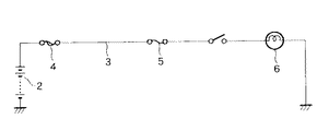
しかしながら、車両における給電および信号送信においては、電源ラインおよび信号ライン(ワイヤハーネス)がドアなどの回転部位を通過したり、移動部位などを通過したり、狭い部位に嵌め込んだり、ビスで止めたり、高温多湿部位などを通過することもあるから、通常の屋内配線より劣化、破断などに起因する短絡(ショート)の可能性が高い。電源ラインまたは信号ラインが短絡すると、これらのラインに異常電流が流れてしまう可能性がある。従来から、図14に示すように、バッテリー2と負荷6との間に配設された電源ライン3に、大容量のメインヒューズ4および小容量のサブヒューズ5を直列に設け、異常電流が流れたときに、ヒューズ,4,5の溶断によって通電を遮断し、電源ライン3を保護している。
【0005】
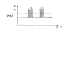
しかしながら、ヒューズは異常電流が一定時間継続しなければ溶断しないため、上述した手法では、図15に示すように断続的に異常電流が生じるレアショートでは、ヒューズが溶断されず、電源ラインを適切に保護できないという問題がある。また、異常電流によって、主機または補機の駆動回路および制御回路が破損する恐れもある。
【0006】
このような問題を解決するために、図16に示すように、バッテリー2と負荷6とを接続する電源ライン11に、遮断スイッチ10および電流測定用微小抵抗8を挿入したシステムが提案されている。このシステムでは、電源ライン11に異常電流が流れると、この異常が、電流測定用微小抵抗8の両側のa点とb点との電位差に現れる。電流監視回路9は、a点とb点との電位差を検出し、この電位差から異常電流が流れていると判断すると、遮断スイッチ10のコイル10aを励磁して、スイッチ10bを開状態に切り換える。図16に示すシステムによれば、図15に示すようなレアショートを検出し、当該検出結果に基づいて遮断スイッチ10を制御して電源ライン11を適切に保護できる。
【0007】
ところで、図16に示すシステムは、電流測定用微小抵抗8の発熱対策が必要であると共に、電源ライン11の容量が大きくなると、装置が大規模化および高価格化するという問題がある。
【0008】
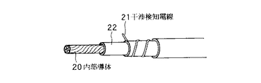
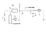
そのため、さらに、図16に示すシステムの問題点を解決するために、図17に示すように、内部導体20の外周に絶縁層22を介して銅箔テープなどの干渉検知電線21を巻き付けた電源ラインを用いて、図18に示す構成で干渉を検知するシステムが提案されている。このシステムでは、内部導体20がボディにショートするとき、それに先立って、干渉検知電線21がボディにショートし、干渉検知電線21の電位がグラウンドに低下して基準電位Vrefより小さくなり、オペアンプ73の出力電圧がマイナスからプラスに反転する。論理回路92は、オペアンプ73の出力電圧を監視することで、干渉検知電線21がボディーにショート(干渉)したことを検出し、その検出結果に基づいて、遮断スイッチ25を切り換えている。しかしながら、このシステムでは、干渉検知電線21は干渉検知のみに用いられており、システムとして無駄が多く経済的でない。
【0009】
本発明は上述した従来技術の問題点に鑑みてなされ、簡単かつ効率的な構成で、電源ラインを電流異常から適切に保護できる車両用電源供給装置を提供することを目的とする。
【0010】
【課題を解決するための手段】
本発明は、上述した目的を達成するために、本発明の車両用電源供給装置は、電源と、前記電源によって駆動される車両搭載装備とを電気的に接続する主電源ラインと、前記主電源ラインの周囲に近接あるいは絶縁層を介して配設され、前記主電源ラインに比べて電流容量が小さい単数または複数の小電流用電源ラインと、前記小電流用電源ライン上の所定の位置に設けられ、当該小電流用電源ラインに異常電流が流れると、接続を遮断する第1の接続遮断手段と、前記主電源ライン上の所定位置に設けられ、前記第1の接続遮断手段が接続状態から遮断状態に切り換わると、それに連動して接続状態から遮断状態に切り換わる第2の接続遮断手段とを有する。
【0011】
本発明の車両用電源分配装置では、例えば、正常時では、第1の接続遮断手段および第2の接続遮断手段の双方は接続状態になっており、主電源ラインを介して、電源が車両搭載装備に供給されると共に、小電流用電源ラインを介して、電子回路駆動用の電源が、車両搭載装備の駆動を制御する電子回路などに供給される。一方、主電源ライン上のある箇所において、例えばボディーへの短絡が生じるとき、それに先立って、小電流用電源ラインがボディーに短絡し、当該小電流用電源ラインに異常電流が流れる。この異常電流によって、第1の接続遮断手段は遮断状態に切り換わる。また、この切り換わりに応じて、第2の接続遮断手段も遮断状態に切り換わる。これによって、主電源ラインを介した電源と車両搭載装備との接続は遮断され、電源から主電源ラインを介して短絡箇所に過剰電流が流れることを回避できる。このとき、小電流用電源ラインは、主電源ラインの短絡を事前に検知する機能に加えて、電子回路駆動用の電源を供給する機能を果たしている。
【0012】
また、本発明の車両用電源供給装置は、好ましくは、前記第1の接続遮断手段は、前記小電流用電源ラインに流れる電流が、所定の電流値を超えると、接続状態から遮断状態に切り換わる。
【0013】
また、本発明の車両用電源供給装置は、好ましくは、前記第1の接続遮断手段は、ヒューズであり、前記第2の接続遮断手段は、前記ヒューズが溶断したか否かを検出する溶断検出手段と、スイッチと、前記溶断検出手段が溶断を検出したときに前記スイッチを閉状態から開状態に切り換える制御手段とを有する。
【0014】
また、本発明の車両用電源供給装置は、好ましくは、前記第1の接続遮断手段は、半導体を用いて構成されるインテリジェント・パワー・スイッチである。
【0015】
また、本発明の車両用電源供給装置は、好ましくは、前記第2の接続遮断手段は、リレースイッチを備えている。
【0016】
また、本発明の車両用電源供給装置は、好ましくは、前記小電流用電源ラインは、電子回路駆動用の電源を供給するラインである。
【0017】
【発明の実施の形態】
以下、本発明の実施形態に係わる車両用電源供給装置について説明する。
第1実施形態
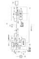
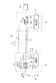
図1は、本実施形態に係わる車両用電源供給装置31の構成図である。図1に示すように、車両用電源供給装置31は、バッテリー43と電源供給部32とが主電源ライン28を介して接続され、電源供給部32と電源被供給部33が主電源ライン41を介して接続され、電源被供給部33と負荷50とが主電源ライン42を介して接続された構成をしている。ここで、主電源ライン41は、小電流用電源ライン29と共に、電源ライン51内に組み込まれている。
【0018】
電源供給部32では、バッテリー43のプラス電極に、主電源ライン28を介して、ヒューズ19、電源遮断部35のスイッチ35aおよびコイル35bの一端が並列に接続されている。また、バッテリー43のプラス電極は、さらに、ヒューズ溶断監視部36および電子部品用電源回路34に接続されている。この他に、バッテリー43のプラス電極は、オルタネータALTの出力に接続され、オルタネータALTが、エンジン回転時に、バッテリー43のプラス電極に接続する負荷および制御部に電力を供給すると共に、その余剰電力でバッテリー43を充電するように構成されている。
【0019】
ヒューズ19の他端は、小電流用電源ライン39の一端に接続されている。小電流用電源ライン39の他端は、小電流用電源ライン29を介して、小電流用電源ライン49に接続されている。ここで、小電流用電源ライン39,29,49は、バッテリー43から電子部品用電源回路44に、メモリをバックアップしたり、電子回路を駆動するための駆動用電源を供給し、電流容量は10A程度で、主電源ライン28,41,42の電流容量50〜100Aに比べて小さい。また、ヒューズ19としては、例えば10A以下の電流で溶断する小容量のものが用いられる。ヒューズ19の両端は、ヒューズ溶断監視部36にも接続されている。ヒューズ溶断監視部36は、ヒューズ下流側の電位監視手段によって、ヒューズ19が溶断したか 否かを検出し、その検出結果を論理回路37に出力する。
【0020】
スイッチ35aの他端は、主電源ライン41の一端に接続されている。コイル35bの他端は、インバータ38を介して論理回路37に接続されている。電子部品用電源回路34は、論理回路37にも接続されている。電子部品用電源回路34は、主電源ライン28から供給された12Vの電源電圧を、DC−DC変換して5Vの電子回路駆動用電圧に変換し、これを論理回路37に供給する。論理回路37は、この電子回路駆動用電圧によって駆動される。論理回路37は、ヒューズ溶断監視部36からの検出結果S19が、溶断したことを示す場合には、インバータ38を介して、コイル35bを消磁し、スイッチ35aを開状態にする。一方、ヒューズ溶断監視部36からの検出結果S19が、溶断していないことを示す場合には、インバータ38を介して、コイル35bを励磁し、スイッチ35aを閉状態にする。
【0021】
電源被供給部33では、主電源ライン41が、電源遮断部45内で、スイッチ45aおよびコイル45bの一端に接続れている。スイッチ45aの他端は、主電源ライン42を介して、負荷50に接続されている。また、コイル45bの他端は、インバータ48を介して、論理回路47に接続されている。さらに、小電流用電源ライン49の他端は、電子部品用電源回路44に接続され、電子部品用電源回路44は論理回路47に接続されている。論理回路47は、信号ライン55を介して、論理回路37に接続されている。
【0022】
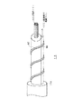
図2は、電源ライン51の内部構成図である。図2に示すように、電源ライン51は、中心導体である主電源ライン41の周囲をPVCなどの絶縁体52で被覆し、絶縁体52の周囲にECU用電源などの小電流用電源ライン29を被覆し、その周囲にさらに樹脂53を被覆して構成される。
【0023】
以下、車両用電源供給装置31の機能について説明する。電源ライン51に異常がない場合には、図1に示すように、論理回路37,47は、それぞれインバータ38,48を介して、コイル35b,45bを消磁しており、スイッチ35a,45aが開状態になっている。そのため、論理回路47によってコイル45bが励磁されており、スイッチ45aが閉状態であるとき、バッテリー43からの電源電流が、主電源ライン28、電源遮断部35、主電源ライン41、電源遮断部45および主電源ライン42を介して、負荷50に供給される。また、主電源ライン28から、ヒューズ19、小電流用電源ライン39および小電流用電源ライン29を介して、電子部品用電源回路44に電子部品の駆動用電流が供給される。
【0024】
ところで、例えば、図1に示す主電源ライン41上のa点がボディにショートする場合には、それに先立って、小電流用電源ライン29がボディ、すなわちグラウンドにショートし、小電流用電源ライン39,29,49に過剰電流が流れる。そのため、ヒューズ19が溶断し、当該溶断がヒューズ溶断監視部36によって検出される。このとき、ヒューズ19としては、10A以下の小容量のものが用いられているため、断続的なショート(レアショート)を敏感に感知し、ヒューズ19を溶断できる。
【0025】
そして、溶断されたことを示す検出結果S19が、ヒューズ溶断監視部36から論理回路37に出力される。論理回路37は、この検出結果S19を入力すると、インバータ38を介して、コイル35bを消磁し、図3に示すように、スイッチ35aを開状態に切り換える。これによって、主電源ライン28と主電源ライン41とは非導通状態になり、主電源ライン41がショートしても、主電源ライン41に異常電流は流れない。また、ヒューズ19は、溶断しているため、主電源ライン28と小電流用電源ライン39とは非導通状態になり、小電流用電源ライン29にも異常電流は流れない。
【0026】
以上説明したように、車両用電源供給装置31によれば、小電流用電源ライン29に接続されたヒューズ19の溶断を監視することで、主電源ライン41の短絡を事前に検出し、短絡箇所を切り離すことができる。また、車両用電源供給装置31によれば、小電流用電源ライン29に、短絡監視機能に加えて、電子部品の駆動用電源を給電する機能を持たせているため、無駄の無い簡単なシステム構成にすることができる。
【0027】
なお、車両用電源供給装置31において、電源ライン51は、図4に示すように、中心導体である主電源ライン41の周囲をPVCなどの絶縁体52で被覆し、絶縁体52の周囲に小電流用電源ライン29を螺旋状に巻き付け、その周囲にさらに樹脂53を被覆した構成にしてもよい。
【0028】
第2実施形態
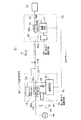
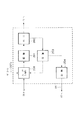
図5は、本実施形態に係わる車両用電源供給装置81の構成図である。なお、図5において、車両用電源供給装置31と同じ構成要素には、図1と同じ符号を付している。車両用電源供給装置81では、電源供給部62内で、主電源ライン28に、IPS(Intelligent Power Switch)61および論理回路67が接続されている。IPS61と電源被供給部63の論理回路77とは、小電流用電源ライン71を介して接続されている。電源遮断部35のスイッチ35aと、電源遮断部45のスイッチ45aとは、主電源ライン72を介して接続されている。また、論理回路67と論理回路77とは、多重伝送ライン73を介して接続されている。ここで、小電流用電源ライン71および主電源ライン72は、例えば、図4に示す電源ライン51と同様に、主電源ライン72の外周に、絶縁層を介して、小電流用電源ライン71を巻き付けて構成され、1本の電源ライン78内に組み込まれている。
【0029】
IPS61は、小電流用電源ライン71を流れる電流を監視し、過電流や定格電流内でも、異常な流れ方をしたときに異常と判断し、小電流用電源ライン71を流れる電流を遮断する半導体素子で構成される。IPS61は、電流が異常であると判断したときにパルスを発生するIPS異常信号S61を論理回路67に出力する。図6は、IPS61の構成図である。図6に示すように、IPS61は、例えば論理回路67からIPS駆動信号S67aを入力する入力ロジック200、駆動回路201および出力回路202を有する。この出力回路202の出力によって、小電流用電源ライン71への給電を駆動あるいは停止する。また、IPS61には、保護回路203および診断回路204が設けられている。保護回路203は、IPS61内の電子回路などを過大電流および過大電圧から保護する。診断回路204は、内部回路状態を診断する。IPS61の実際の製品としては、例えば、東芝製、TPD1004Sを参照されたい。IPS61は、論理回路67からIPS駆動信号S67aを入力し、このIPS駆動信号S67aがハイレベルのときに駆動状態となり、ローレベルのときに停止状態になる。なお、IPS61は、発熱を監視して電流を遮断するものでもよい。
【0030】
図7は、論理回路47の構成図である。図7に示すように、論理回路47は、DC−DCコンバータ82、マイクロコンピュータ83、多重伝送回路84およびバスインタフェース回路85を備えている。DC−DCコンバータ82は、主電源ライン28を介してバッテリー43から入力した12Vの電源電圧を5Vの電子回路駆動用電圧に変換し、これをマイクロコンピュータ83に供給する。マイクロコンピュータ83は、DC−DCコンバータ82からの電子回路駆動用電圧によって駆動し、後述するように、IPS異常信号S61に発生したパルスを検出すると、インバータ38を介してコイル35bを消磁し、スイッチ35aを開状態にする。また、マイクロコンピュータ83は、多重伝送回路84、バスインタフェース回路85および多重伝送ライン73を介して、論理回路77に多重信号を出力する。
【0031】
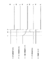
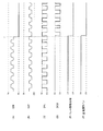
以下、図5〜図8を参照して、車両用電源供給装置81の動作について説明する。図8は、図5に示す電源ライン78のa点において破損が生じた場合における各信号およびラインの電位のタイミングチャートである。図5に示す電源ライン78がa点で破損すると、先ず、小電流用電源ライン71がボディに短絡し、図8(C)に示すように、時刻t1に、小電流用電源ライン71の電位が低下すると共に、小電流用電源ライン71に過剰電流が流れる。この過剰電流は、IPS61において検知され、図8(D)に示すように、時刻t2に、IPS異常信号S61にパルスが発生する。論理回路67は、IPS異常信号S61に含まれるパルスを検出すると、時刻t3に、IPS駆動信号S67aをおよびリレー駆動信号S67bをハイレベルからローレベルに切り換える。これによって、IPS61は、主電源ライン28と小電流用電源ライン71とを遮断した状態を保持し、電源遮断部35のコイル35bは消磁され、スイッチ35aは開状態になり、主電源ライン72の電位は、ハイレベルからローレベンルに切り換わる。
【0032】
以上説明したように、車両用電源供給装置81によれば、小電流用電源ライン71に接続されたIPS61からの検出結果に基づいて、主電源ライン71の短絡を事前に検出し、短絡箇所を切り離すことができる。また、車両用電源供給装置81によれば、小電流用電源ライン71に、短絡監視機能に加えて、電子部品の駆動用電流を伝送する機能を持たせているため、無駄の無い簡単なシステム構成にすることができる。
【0033】
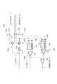
第3実施形態
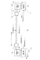
図9は、本実施形態に係わる車両用電源供給装置91の構成図である。図9に示すように、多重伝送ライン96,97に対して、図中左側に、多重伝送回路92、制御回路93およびバスインタフェース94で構成される端末110が配設されている。また、多重伝送ライン96,97に対して、図中右側に、多重伝送回路102、制御回路103およびバスインタフェース104で構成される端末111が配設されている。ここで、多重伝送回路92と制御回路93とは、データ伝送ライン95および異常信号ライン98を介して接続され、多重伝送回路92とバスインタフェース94とは、送信ラインTxおよび受信ラインRxを介して接続されている。さらに、バスインタフェース94と制御回路93とは、異常信号ライン99を介して接続されている。
【0034】
なお、図9には図示しないが、端末110と端末111との間には、多重伝送ライン96,97に加えて、図10に示すように、主電源ライン112および回路駆動用電源ライン113が配設される。これらのラインは、主電源ライン112および回路駆動用電源ライン113の双方を、平行に位置する多重伝送ライン96,97を巻き付け、保護層114で被覆してワイヤハーネス115内に組み込まれている。ところで、多重伝送ライン96,97は、ツイストペア線を構成するように、ワイヤハーネス115内に組み込んでもよい。このように、多重伝送ライン96および多重伝送ライン97を用いて後述するように、レベルが相互に反転した実質的に同一の信号を送信することで、電送中に生じる同相ノイズの影響を抑制できると共に、一方の多重伝送ラインがショートしても、他方の多重電送ラインを介して信号を送信できる。
【0035】
多重伝送回路92は、データ伝送ライン95を介して制御回路93から入力したパラレル信号を図11(A)に示すような時分割のシリアル信号に変換し、このシリアル信号を、送信ラインTxを介して、バスインタフェース94に出力する。このシリアル信号は、最初の2ビットがデータ本体の開始を示しており、それに続く8ビットがデータ本体を示している。データ本体の変調には、1ビットを3つの位相に分割して、第1の位相を常にハイレベルとし、第2の位相をデータの値に応じてローレベルまたはハイレベルとし、第3の位相を常にローレベルとするPWM(Pulse Width Modulation)が用いられている。
【0036】
図12は、バスインタフェース94の構成図である。なお、端末111のバスインタフェース104は、バスインタフェース94と同じ構成をしている。図12に示すように、バスインタフェース94内には、送信回路94a、受信回路94bおよび受信回路94cが内蔵されている。送信回路94a内では、送信ラインTxが、電流源121に接続されると共に、インバータ120を介して電流源122に接続されている。従って、送信ラインTxのレベルに応じた電圧が電流源121に印加されると共に、送信ラインTxのレベルを反転したレベルに応じた電圧が電流源122に印加される。
【0037】
電流源121,122は、印加された電圧に比例した電流を、それぞれ伝送ライン123,124に出力する。ここで、伝送ライン123は抵抗136を介してグランドに接続され、伝送ライン124は抵抗135を介して電源電圧に接続されている。図11(A)に示す時分割のシリアル信号が送信ラインTxを介して電流源121に入力されると、このシリアル信号に応じて、電流源121から伝送ライン123に出力される電流が変動し、抵抗136のバイアス機能によって、伝送ライン123および多重伝送ライン96の電位は、図11(B)に示すようになる。また、図11(A)に示す時分割のシリアル信号を反転したシリアル信号が、インバータ120を介して電流源122に入力されると、抵抗135のバイアス機能によって、伝送ライン124および多重伝送ライン97の電位は、図11(C)に示すようになる。
【0038】
また、受信回路94b内では、伝送ライン123が、コンデンサ125を介して、パルスレベル設定回路129の一方の入力端子に接続され、その出力端子がコンパレータ131の+入力端子に接続されている。また、伝送ライン124が、コンデンサ126を介して、パルスレベル設定回路129の他方の入力端子に接続され、その出力端子がコンパレータ131の−入力端子に接続されている。コンパレータ131は、+入力端子の電位と、−入力端子の電位との差分電圧を受信信号として、出力端子から受信ラインRxに出力する。受信信号は、排他的論理和(XOR)回路133の一方の入力端子にも出力される。ここで、受信回路94bは、多重伝送ライン96および97のうち、一方に短絡などの故障が生じた場合であっても、他方の多重伝送ラインを介して受信した受信信号を判別して、受信ラインRxを介して多重伝送回路92に出力するように、パルスレベル設定回路129において受信信号のレベルを設定している。多重伝送回路92は、受信ラインRxを介して、入力した受信信号を、シリアル信号からパラレル信号に変換し、データ伝送ライン95を介して、制御回路93に出力する。
【0039】
さらに、受信回路94c内では、伝送ライン123が、コンデンサ127を介して、パルスレベル設定回路130の一方の入力端子に接続され、その出力端子がコンパレータ132の+入力端子に接続されている。また、伝送ライン124が、コンデンサ128を介して、パルスレベル設定回路130の他方の入力端子に接続され、その出力端子がコンパレータ132の−入力端子に接続されている。コンパレータ132は、+入力端子の電位と、−入力端子の電位との差分電圧を受信信号として、出力端子から、排他的論理和回路133の他方の入力端子に出力する。ここで、受信回路94cは、多重伝送ライン96および97の双方から正確な受信信号を受信しないと、受信信号を判別できないように、パルスレベル設定回路130において受信信号のレベルを設定している。
【0040】
排他的論理和回路133は、コンパレータ131およびコンパレータ132の双方の出力端子から、受信信号を入力し、その排他的論理和を演算し、演算結果を異常信号として、異常信号ライン99を介して制御回路93に出力する。具体的には、排他的論理和回路133からの異常信号は、受信信号の双方が同一であればハイレベル、異なればローレベルとなる。
【0041】
以下、図9に示す車両用電源供給装置91において、a点で多重伝送ライン97が、ボディと干渉し、グランドに短絡した場合の動作を説明する。図13は、a点で多重伝送ライン97が短絡した場合における車両用信号伝送装置91の各信号の波形図である。なお、多重伝送ライン96,97の短絡は、図10に示すワイヤハーネス115の構造上、通常、主電源ライン112および回路駆動用電源ライン113の短絡に先立って発生する。図13に示す時刻t1に、多重伝送ライン96上のa点が短絡すると、多重伝送ライン96および97を介して端末110から端末111に伝送される送信信号S96およびS97の電位の波形は、図13(A)および(B)に示すようになる。このとき、端末111のバスインタフェース104内で、多重伝送ライン97を介して受信した送信信号S97に基づいて、図12に示す受信回路94bに対応する受信回路において、図13(C)に示す受信信号SRxが生成され、この受信信号SRxが受信ラインRxを介して、多重伝送回路102に出力される。
【0042】
一方、図12に示す受信回路94cに対応する受信回路において生成される異常信号S150は、図13(D)に示すように、時刻t1に、ハイレベルからローレベルに切り換わる。制御回路103は、受信回路94cから入力した異常信号S150がハイレベルからローレベルに切り換わったことを検出すると、図13(E)に示すように、リレー駆動信号をハイレベルからローレベルに切り換える。このリレー駆動信号は、制御回路103から、端末111に電源を供給する図10に示す主電源ライン112上に設けられたリレースイッチ(図示せず)に出力される。このリレースイッチは、リレー駆動信号がハイレベルからローレベルに切り換わると、接続状態から遮断状態に切り換わる。これによって、主電源ライン112の電位は、図13(F)に示すように、12Vから0Vに落ちる。なお、図10に示す回路駆動用電源ライン113上にも、リレースイッチを設け、制御回路103からのリレー駆動信号に基づいて、このリレースイッチを遮断状態にしてもよい。
【0043】
ところで、図9に示すa点で、多重伝送ライン96および97の双方が同時に短絡した場合には、バスインタフェース104は、送信信号を全く受信しなくなる。制御回路103は、バスインタフェース104が送信信号を一定時間受信しない場合に、リレー駆動信号をハイレベルからローレベルに切り換え、主電源ライン112を遮断する。制御回路103は、例えば、通信サイクルが50msのときに、100msの間、送信信号を受信しないと、リレー駆動信号をハイレベルからローレベルに切り換える。
【0044】
以上説明したように、車両用電源供給装置91によれば、多重伝送ライン96,97を介して端末111が受信した受信結果に基づいて、図10に示す主電源ライン112および回路駆動用電源ライン113の短絡を事前に検出し、短絡箇所を切り離すことができる。また、車両用電源供給装置91によれば、多重伝送ライン96,97は、短絡監視機能の他に、多重信号伝送機能を持っており、無駄の無い簡単なシステム構成にすることができる。
【0045】
本発明は上述した実施形態には限定されない。例えば、上述した実施形態では、電源供給部および電源被供給部や、2個の端末相互間でのデータ通信を例示したが、単数の電源供給部と複数の電源被供給部とが接続されている場合や、3以上の端末が多対多あるいは1対多で接続されている場合にも本発明は適用できる。
【0046】
また、上述した実施形態では、第1の接続遮断手段として、ヒューズやIPSを例示したが、小電流用電源ラインの異常を検出し、接続を遮断するものであれば、その他の接続遮断手段を用いてもよい。
【0047】
【発明の効果】
以上説明したように、車両用電源供給装置によれば、主電源ラインに障害が生じる前に、主電源ラインを介した電源と車両搭載装備との接続が遮断され、主電源ラインを介して電源から障害箇所に過剰電流が流れることを回避できる。また、本発明の車両用電源供給装置によれば、小電流用電源ラインは、主電源ラインの短絡を事前に検知する機能に加えて、電子回路駆動用の電源を供給する機能および信号伝送機能を果たしており、簡単で無駄のないシステム構成にすることができる。
【図面の簡単な説明】
【図1】図1は、本発明の第1実施形態に係わる車両用電源供給装置の正常状態での構成図である。
【図2】図2は、図1に示す電源ラインの内部構成図である。
【図3】図3は、図1に示す車両用電源供給装置が異常状態になったときの構成図である。
【図4】図4は、図1に示す電源ラインのその他の内部構成図である。
【図5】図5は、本発明の第2実施形態に係わる車両用電源供給装置の構成図である。
【図6】図6は、IPSの構成図である。
【図7】図7は、図5に示す論理回路の構成図である。
【図8】図8は、図5に示す電源ラインのa点において破損が生じた場合における各信号およびラインの電位のタイミングチャートである。
【図9】図9は、本発明の第3実施形態に係わる車両用電源供給装置の構成図である。
【図10】図9に示す多重伝送ラインを組み込んだワイヤハーネスの構造を説明するための図である。
【図11】(A)は送信ラインTxを介して伝送される送信信号の波形図、(B)は第1の伝送ラインを流れる電流の波形図、(C)は第2の伝送ラインを流れる電流の波形図である。
【図12】図12は、図9に示すバスインタフェースの構成図である。
【図13】図13は、図9に示すa点で第1の多重伝送ラインが短絡した場合の各信号およびラインの波形図である。
【図14】図14は、従来の車両用電源供給装置を説明するための図である。
【図15】図15は、電源ラインに生じるレアショートを説明するための図である。
【図16】図16は、従来のその他の車両用電源供給装置を説明するための図である。
【図17】図17は、従来の車両用電源供給装置に用いられる干渉検知電線の構造を説明するための図である。
【図18】図18は、図17に示す干渉検知電線を用いた車両用電源供給装置を説明するための図である。
【符号の説明】
31,81,91…車両用電源供給装置
29,71…小電流用電源ライン
32,62…電源供給部
33,63…電源被供給部
41,72…主電源ライン
43…バッテリー
35,45…電源遮断部
50…負荷
51…電源ライン
73…多重伝送ライン
96,97…多重伝送ライン
110,111…端末[0001]
BACKGROUND OF THE INVENTION
The present invention relates to a power supply device for a vehicle that can appropriately protect a power supply line installed in a vehicle such as an automobile from an abnormal current with a simple configuration.
[0002]
[Background Art and Problems to be Solved by the Invention]
Recently, with the rapid computerization of vehicles, for vehicles, for example, various passenger cars, improvement of fuel consumption of main equipment (hereinafter referred to as main engine) essential for operation of internal combustion engine, automatic transmission, etc., reduction of exhaust gas. From the viewpoints of smooth running, safe running, etc., electronic circuits and electronic devices including a microcomputer are mounted. In addition, the front panel instruments are replaced with electronic display devices, for example, color liquid crystal display devices, to make it easier to recognize the operation state of the vehicle and to provide various types of vehicle information. There are also attempts. Furthermore, there is a high demand for using the vehicle not only as a moving means but also as a living space as well as improving the ride comfort and convenience of the vehicle as a moving means. Auxiliary equipment / equipment (hereinafter referred to as “auxiliary”) such as position evaluation / operation guidance device, automatic seat adjustment device, power window, wiper, door lock, various lamps, radio, CD, TV device, entertainment facility, etc. Increasing mounting and electronic control of them are progressing.
[0003]
As described above, as the electrical equipment, the main engine, and the auxiliary equipment mounted on the vehicle are electronically controlled, the number of parts in which the electrical equipment, the main equipment, and the auxiliary equipment are electrically driven increases, and the main equipment and the auxiliary equipment. Various electronic devices are mounted on the vehicle for electronic control. Therefore, for the devices and devices mounted on the main engine, power transmission in the vehicle and signal transmission for operating the electronic control device have become important.
[0004]
However, in power feeding and signal transmission in a vehicle, the power line and signal line (wire harness) pass through a rotating part such as a door, pass through a moving part, etc., fit into a narrow part, or stop with a screw. Since it may pass through hot and humid parts, there is a higher possibility of a short circuit due to deterioration, breakage, etc. than ordinary indoor wiring. When the power supply line or the signal line is short-circuited, an abnormal current may flow through these lines. Conventionally, as shown in FIG. 14, a large-capacity
[0005]
However, since the fuse does not blow unless the abnormal current continues for a certain period of time, in the above-described method, the fuse is not blown in the rare short in which the abnormal current is intermittently generated as shown in FIG. There is a problem that it cannot be protected. Further, the drive circuit and control circuit of the main machine or auxiliary machine may be damaged by the abnormal current.
[0006]
In order to solve such a problem, as shown in FIG. 16, a system has been proposed in which a cut-
[0007]
Incidentally, the system shown in FIG. 16 needs to take measures against heat generation of the
[0008]
Therefore, in order to further solve the problem of the system shown in FIG. 16, as shown in FIG. 17, a power source in which an interference detection electric wire 21 such as a copper foil tape is wound around the outer periphery of the
[0009]
The present invention has been made in view of the above-described problems of the prior art, and an object thereof is to provide a vehicular power supply device that can appropriately protect a power supply line from a current abnormality with a simple and efficient configuration.
[0010]
[Means for Solving the Problems]
In order to achieve the above-described object, the present invention provides a vehicle power supply apparatus according to the present invention, wherein a main power line for electrically connecting a power source and a vehicle-mounted equipment driven by the power source, and the main power source One or a plurality of small current power supply lines disposed near the line or via an insulating layer and having a smaller current capacity than the main power supply line, and provided at predetermined positions on the small current power supply line When an abnormal current flows through the small current power line, a first connection blocking means for cutting the connection and a predetermined position on the main power supply line are provided, and the first connection blocking means is disconnected from the connected state. And a second connection blocking means for switching from the connected state to the blocked state in conjunction with the switching to the blocked state.
[0011]
In the power distribution device for a vehicle according to the present invention, for example, at the normal time, both the first connection blocking means and the second connection blocking means are in a connected state, and the power is mounted on the vehicle via the main power line. In addition to being supplied to the equipment, the power for driving the electronic circuit is supplied to an electronic circuit for controlling the driving of the equipment mounted on the vehicle via a power supply line for small current. On the other hand, for example, when a short circuit to the body occurs at a certain point on the main power supply line, the small current power supply line is shorted to the body prior to the short circuit, and an abnormal current flows through the small current power supply line. Due to this abnormal current, the first connection cutoff means is switched to the cutoff state. Further, in response to this switching, the second connection blocking means also switches to the blocking state. As a result, the connection between the power supply and the vehicle-mounted equipment via the main power supply line is cut off, and it is possible to avoid an excessive current from flowing from the power supply to the short-circuited location via the main power supply line. At this time, the power supply line for small current fulfills the function of supplying power for driving the electronic circuit in addition to the function of detecting the short circuit of the main power supply line in advance.
[0012]
In the vehicular power supply device of the present invention, it is preferable that the first connection cut-off unit switches the connection state from the connection state to the cut-off state when a current flowing through the small current power line exceeds a predetermined current value. Change.
[0013]
In the vehicle power supply device according to the present invention, preferably, the first connection cutoff means is a fuse, and the second connection cutoff means detects whether or not the fuse is blown. Means, a switch, and control means for switching the switch from the closed state to the open state when the fusing detection means detects fusing.
[0014]
In the vehicular power supply device of the present invention, it is preferable that the first connection cutoff means is an intelligent power switch configured using a semiconductor.
[0015]
In the vehicular power supply apparatus of the present invention, it is preferable that the second connection cutoff means includes a relay switch.
[0016]
In the vehicular power supply device of the present invention, it is preferable that the small current power line is a line for supplying power for driving an electronic circuit.
[0017]
DETAILED DESCRIPTION OF THE INVENTION
Hereinafter, a vehicle power supply apparatus according to an embodiment of the present invention will be described.
First embodiment
FIG. 1 is a configuration diagram of a vehicle
[0018]
In the
[0019]
The other end of the
[0020]
The other end of the
[0021]
In the power supplied
[0022]
FIG. 2 is an internal configuration diagram of the
[0023]
Hereinafter, the function of the vehicle
[0024]
By the way, for example, when point a on the main
[0025]
Then, a detection result S19 indicating that the fuse has been blown is output from the fuse
[0026]
As described above, according to the vehicle
[0027]
In the vehicle
[0028]
Second embodiment
FIG. 5 is a configuration diagram of the vehicle
[0029]
The
[0030]
FIG. 7 is a configuration diagram of the
[0031]
Hereinafter, the operation of the vehicle
[0032]
As described above, according to the vehicle
[0033]
Third embodiment
FIG. 9 is a configuration diagram of the vehicle
[0034]
Although not shown in FIG. 9, in addition to the
[0035]
The
[0036]
FIG. 12 is a configuration diagram of the
[0037]
The
[0038]
In the receiving
[0039]
Further, in the receiving
[0040]
The exclusive OR
[0041]
The operation when the
[0042]
On the other hand, the abnormal signal S150 generated in the receiving circuit corresponding to the receiving
[0043]
By the way, when both of the
[0044]
As described above, according to the vehicle
[0045]
The present invention is not limited to the embodiment described above. For example, in the above-described embodiment, the power supply unit and the power supply unit and the data communication between two terminals are illustrated, but a single power supply unit and a plurality of power supply units are connected. The present invention can also be applied when there are three or more terminals connected in a many-to-many or one-to-many manner.
[0046]
Further, in the above-described embodiment, the fuse and the IPS are exemplified as the first connection cutoff unit. However, if the abnormality is detected in the power supply line for small current and the connection is cut off, other connection cutoff units are used. It may be used.
[0047]
【The invention's effect】
As described above, according to the vehicle power supply device, the connection between the power supply via the main power supply line and the equipment mounted on the vehicle is interrupted before the main power supply line fails, and the power supply via the main power supply line is interrupted. Therefore, it is possible to avoid an excessive current from flowing to the fault location. Moreover, according to the vehicle power supply device of the present invention,The power line for small current is a short circuit of the main power lineIn addition to the function of detecting the power in advance, the function of supplying power for driving the electronic circuit and the function of signal transmission are fulfilled, and a simple and lean system configuration can be achieved.
[Brief description of the drawings]
FIG. 1 is a configuration diagram of a vehicle power supply device according to a first embodiment of the present invention in a normal state.
FIG. 2 is an internal configuration diagram of a power supply line shown in FIG. 1;
FIG. 3 is a configuration diagram when the vehicular power supply device shown in FIG. 1 enters an abnormal state.
FIG. 4 is another internal configuration diagram of the power supply line shown in FIG. 1;
FIG. 5 is a configuration diagram of a vehicle power supply device according to a second embodiment of the present invention.
FIG. 6 is a block diagram of an IPS.
FIG. 7 is a configuration diagram of the logic circuit shown in FIG. 5;
8 is a timing chart of signals and line potentials when damage occurs at point a of the power supply line shown in FIG. 5; FIG.
FIG. 9 is a configuration diagram of a vehicle power supply device according to a third embodiment of the present invention.
10 is a view for explaining the structure of a wire harness incorporating the multiplex transmission line shown in FIG. 9;
11A is a waveform diagram of a transmission signal transmitted through the transmission line Tx, FIG. 11B is a waveform diagram of a current flowing through the first transmission line, and FIG. 11C is a waveform flowing through the second transmission line. It is a waveform diagram of current.
FIG. 12 is a block diagram of the bus interface shown in FIG. 9;
13 is a waveform diagram of each signal and line when the first multiplex transmission line is short-circuited at a point a shown in FIG. 9;
FIG. 14 is a diagram for explaining a conventional vehicle power supply device;
FIG. 15 is a diagram for explaining a rare short that occurs in a power supply line;
FIG. 16 is a diagram for explaining another conventional vehicle power supply device.
FIG. 17 is a diagram for explaining the structure of an interference detection electric wire used in a conventional vehicle power supply device.
FIG. 18 is a diagram for explaining a vehicle power supply device using the interference detection electric wire shown in FIG. 17;
[Explanation of symbols]
31, 81, 91 ... Vehicle power supply device
29, 71 ... Power line for small current
32, 62 ... power supply section
33, 63 ... Power supply section
41, 72 ... main power line
43 ... Battery
35, 45 ... Power shut-off section
50 ... load
51 ... Power line
73. Multiple transmission lines
96, 97 ... Multiple transmission lines
110, 111 ... terminal
Claims (6)
前記電源によって駆動される車両搭載装備とを電気的に接続する主電源ラインと、
前記主電源ラインの周囲に近接あるいは絶縁層を介して配設され、前記主電源ラインに比べて電流容量が小さい単数または複数の小電流用電源ラインと、
前記小電流用電源ライン上の所定の位置に設けられ、当該小電流用電源ラインに異常電流が流れると、接続を遮断する第1の接続遮断手段と、
前記主電源ライン上の所定位置に設けられ、前記第1の接続遮断手段が接続状態から遮断状態に切り換わると、それに連動して接続状態から遮断状態に切り換わる第2の接続遮断手段とを有する車両用電源供給装置。Power supply,
A main power line for electrically connecting the on-vehicle equipment driven by the power source;
One or a plurality of power supply lines for small current, which are arranged near the main power supply line or via an insulating layer, and have a smaller current capacity than the main power supply line,
A first connection disconnecting means which is provided at a predetermined position on the small current power line, and disconnects the connection when an abnormal current flows through the small current power line;
A second connection blocking means provided at a predetermined position on the main power supply line, wherein the first connection blocking means switches from the connected state to the blocked state in conjunction with the switching from the connected state to the blocked state; A power supply device for a vehicle.
前記第2の接続遮断手段は、前記ヒューズが溶断したか否かを検出する溶断検出手段と、スイッチと、前記溶断検出手段が溶断を検出したときに前記スイッチを閉状態から開状態に切り換える制御手段とを有する請求項2に記載の車両用電源供給装置。The first connection blocking means is a fuse;
The second connection cut-off means includes a fusing detection means for detecting whether or not the fuse is blown, a switch, and a control for switching the switch from a closed state to an open state when the fusing detection means detects a fusing. The vehicle power supply device according to claim 2, further comprising: means.
Priority Applications (1)
| Application Number | Priority Date | Filing Date | Title |
|---|---|---|---|
| JP12583797A JP3644792B2 (en) | 1997-05-15 | 1997-05-15 | Vehicle power supply device |
Applications Claiming Priority (1)
| Application Number | Priority Date | Filing Date | Title |
|---|---|---|---|
| JP12583797A JP3644792B2 (en) | 1997-05-15 | 1997-05-15 | Vehicle power supply device |
Publications (2)
| Publication Number | Publication Date |
|---|---|
| JPH10322880A JPH10322880A (en) | 1998-12-04 |
| JP3644792B2 true JP3644792B2 (en) | 2005-05-11 |
Family
ID=14920176
Family Applications (1)
| Application Number | Title | Priority Date | Filing Date |
|---|---|---|---|
| JP12583797A Expired - Fee Related JP3644792B2 (en) | 1997-05-15 | 1997-05-15 | Vehicle power supply device |
Country Status (1)
| Country | Link |
|---|---|
| JP (1) | JP3644792B2 (en) |
Families Citing this family (12)
| Publication number | Priority date | Publication date | Assignee | Title |
|---|---|---|---|---|
| KR20010103998A (en) * | 2000-05-12 | 2001-11-24 | 이계안 | Curren leakage preventy system and method for hybrid electric vehicle |
| JP2003002040A (en) * | 2001-06-22 | 2003-01-08 | Masahiro Kawamichi | Method and device for cooling inside of vehicle |
| JP4687743B2 (en) | 2008-05-02 | 2011-05-25 | ソニー株式会社 | Battery pack and control method |
| JP2013218996A (en) * | 2012-04-06 | 2013-10-24 | Okuda Ichiyoshi | Structure of entangling outside line of cable in spiral |
| JP6124630B2 (en) * | 2013-03-15 | 2017-05-10 | 矢崎総業株式会社 | Vehicle power shut-off device |
| US11070049B2 (en) | 2017-11-08 | 2021-07-20 | Eaton Intelligent Power Limited | System, method, and apparatus for power distribution in an electric mobile application using a combined breaker and relay |
| US11108225B2 (en) | 2017-11-08 | 2021-08-31 | Eaton Intelligent Power Limited | System, method, and apparatus for power distribution in an electric mobile application using a combined breaker and relay |
| CN111448731B (en) | 2017-11-08 | 2023-06-30 | 伊顿智能动力有限公司 | Power distribution unit and fuse management for electric mobile applications |
| US11368031B2 (en) | 2017-11-08 | 2022-06-21 | Eaton Intelligent Power Limited | Power distribution and circuit protection for a mobile application having a high efficiency inverter |
| US11670937B2 (en) | 2019-02-22 | 2023-06-06 | Eaton Intelligent Power Limited | Coolant connector having a chamfered lip and fir tree axially aligned with at least one o-ring |
| CN114825261B (en) * | 2022-04-26 | 2024-05-10 | 湖南麦格米特电气技术有限公司 | Short-circuit protection circuit, power supply device and electronic device |
| CN115173372A (en) * | 2022-07-26 | 2022-10-11 | 广州小鹏汽车科技有限公司 | Short-circuit protection circuit, power battery pack and vehicle |
-
1997
- 1997-05-15 JP JP12583797A patent/JP3644792B2/en not_active Expired - Fee Related
Also Published As
| Publication number | Publication date |
|---|---|
| JPH10322880A (en) | 1998-12-04 |
Similar Documents
| Publication | Publication Date | Title |
|---|---|---|
| US8829717B2 (en) | Battery control device and battery system | |
| US11447031B2 (en) | Electric vehicle charging apparatus | |
| CN106537712B (en) | The equipment that high pressure onboard power system for monitoring electro-motive vehicle overloads | |
| US8518570B2 (en) | Battery system | |
| US7791310B2 (en) | Vehicle electrical system including battery state of charge detection on the positive terminal of the battery | |
| US6020811A (en) | Apparatus for multiplexing between on-board units in a vehicle | |
| JP3644792B2 (en) | Vehicle power supply device | |
| EP1332924A1 (en) | Device for protecting the start battery of a vehicle and the electrical network supplying said battery | |
| JP3949406B2 (en) | Electrical connection device for vehicle | |
| KR20150023040A (en) | Charging/discharging device | |
| JP7422670B2 (en) | Power system and management device | |
| WO2010113927A1 (en) | Electric vehicle charger and ground fault detection method | |
| US10608575B2 (en) | Abnormality diagnosis apparatus | |
| CN109302852A (en) | Managing device and power-supply system | |
| EP2840405B1 (en) | In-vehicle power source apparatus | |
| JPH09275635A (en) | Power distribution system | |
| JP3499379B2 (en) | Power distribution system | |
| JPH10341524A (en) | Signal transmitter for mounting on vehicle, and signal transmission method, and power supply controller for mounting on vehicle, and power method, and cable abnormality detector for mounting on vehicle | |
| KR101257923B1 (en) | Automatic power disconnecting apparatus | |
| JP3468697B2 (en) | Vehicle power supply | |
| CN106300229A (en) | A kind of for protecting equipment and the method for high-tension battery electricity system | |
| JP3379081B2 (en) | Power distribution device for vehicles | |
| JP3734918B2 (en) | Power distribution device for vehicles | |
| JP2001119960A (en) | Method and device for urgently interrupting vehicle feeder circuit and vehicle voltage converter | |
| US10948530B2 (en) | Apparatus and method for asymmetrical isolation monitor failure detection |
Legal Events
| Date | Code | Title | Description |
|---|---|---|---|
| A977 | Report on retrieval |
Free format text: JAPANESE INTERMEDIATE CODE: A971007 Effective date: 20040129 |
|
| A131 | Notification of reasons for refusal |
Free format text: JAPANESE INTERMEDIATE CODE: A131 Effective date: 20040203 |
|
| A521 | Written amendment |
Free format text: JAPANESE INTERMEDIATE CODE: A523 Effective date: 20040405 |
|
| A02 | Decision of refusal |
Free format text: JAPANESE INTERMEDIATE CODE: A02 Effective date: 20041102 |
|
| RD05 | Notification of revocation of power of attorney |
Free format text: JAPANESE INTERMEDIATE CODE: A7425 Effective date: 20041202 |
|
| A521 | Written amendment |
Free format text: JAPANESE INTERMEDIATE CODE: A523 Effective date: 20041222 |
|
| A911 | Transfer of reconsideration by examiner before appeal (zenchi) |
Free format text: JAPANESE INTERMEDIATE CODE: A911 Effective date: 20041228 |
|
| TRDD | Decision of grant or rejection written | ||
| A01 | Written decision to grant a patent or to grant a registration (utility model) |
Free format text: JAPANESE INTERMEDIATE CODE: A01 Effective date: 20050128 |
|
| A61 | First payment of annual fees (during grant procedure) |
Free format text: JAPANESE INTERMEDIATE CODE: A61 Effective date: 20050201 |
|
| FPAY | Renewal fee payment (event date is renewal date of database) |
Free format text: PAYMENT UNTIL: 20080210 Year of fee payment: 3 |
|
| FPAY | Renewal fee payment (event date is renewal date of database) |
Free format text: PAYMENT UNTIL: 20090210 Year of fee payment: 4 |
|
| FPAY | Renewal fee payment (event date is renewal date of database) |
Free format text: PAYMENT UNTIL: 20090210 Year of fee payment: 4 |
|
| FPAY | Renewal fee payment (event date is renewal date of database) |
Free format text: PAYMENT UNTIL: 20100210 Year of fee payment: 5 |
|
| FPAY | Renewal fee payment (event date is renewal date of database) |
Free format text: PAYMENT UNTIL: 20100210 Year of fee payment: 5 |
|
| FPAY | Renewal fee payment (event date is renewal date of database) |
Free format text: PAYMENT UNTIL: 20110210 Year of fee payment: 6 |
|
| FPAY | Renewal fee payment (event date is renewal date of database) |
Free format text: PAYMENT UNTIL: 20120210 Year of fee payment: 7 |
|
| FPAY | Renewal fee payment (event date is renewal date of database) |
Free format text: PAYMENT UNTIL: 20130210 Year of fee payment: 8 |
|
| FPAY | Renewal fee payment (event date is renewal date of database) |
Free format text: PAYMENT UNTIL: 20130210 Year of fee payment: 8 |
|
| FPAY | Renewal fee payment (event date is renewal date of database) |
Free format text: PAYMENT UNTIL: 20140210 Year of fee payment: 9 |
|
| LAPS | Cancellation because of no payment of annual fees |