JP3642263B2 - Liquid crystal device and electronic device - Google Patents
Liquid crystal device and electronic device Download PDFInfo
- Publication number
- JP3642263B2 JP3642263B2 JP2000151666A JP2000151666A JP3642263B2 JP 3642263 B2 JP3642263 B2 JP 3642263B2 JP 2000151666 A JP2000151666 A JP 2000151666A JP 2000151666 A JP2000151666 A JP 2000151666A JP 3642263 B2 JP3642263 B2 JP 3642263B2
- Authority
- JP
- Japan
- Prior art keywords
- liquid crystal
- light
- crystal device
- flexible substrate
- light emitting
- Prior art date
- Legal status (The legal status is an assumption and is not a legal conclusion. Google has not performed a legal analysis and makes no representation as to the accuracy of the status listed.)
- Expired - Lifetime
Links
Images


Classifications
-
- G—PHYSICS
- G02—OPTICS
- G02F—OPTICAL DEVICES OR ARRANGEMENTS FOR THE CONTROL OF LIGHT BY MODIFICATION OF THE OPTICAL PROPERTIES OF THE MEDIA OF THE ELEMENTS INVOLVED THEREIN; NON-LINEAR OPTICS; FREQUENCY-CHANGING OF LIGHT; OPTICAL LOGIC ELEMENTS; OPTICAL ANALOGUE/DIGITAL CONVERTERS
- G02F1/00—Devices or arrangements for the control of the intensity, colour, phase, polarisation or direction of light arriving from an independent light source, e.g. switching, gating or modulating; Non-linear optics
- G02F1/01—Devices or arrangements for the control of the intensity, colour, phase, polarisation or direction of light arriving from an independent light source, e.g. switching, gating or modulating; Non-linear optics for the control of the intensity, phase, polarisation or colour
- G02F1/13—Devices or arrangements for the control of the intensity, colour, phase, polarisation or direction of light arriving from an independent light source, e.g. switching, gating or modulating; Non-linear optics for the control of the intensity, phase, polarisation or colour based on liquid crystals, e.g. single liquid crystal display cells
- G02F1/133—Constructional arrangements; Operation of liquid crystal cells; Circuit arrangements
- G02F1/1333—Constructional arrangements; Manufacturing methods
- G02F1/1335—Structural association of cells with optical devices, e.g. polarisers or reflectors
- G02F1/1336—Illuminating devices
- G02F1/133615—Edge-illuminating devices, i.e. illuminating from the side
-
- G—PHYSICS
- G02—OPTICS
- G02F—OPTICAL DEVICES OR ARRANGEMENTS FOR THE CONTROL OF LIGHT BY MODIFICATION OF THE OPTICAL PROPERTIES OF THE MEDIA OF THE ELEMENTS INVOLVED THEREIN; NON-LINEAR OPTICS; FREQUENCY-CHANGING OF LIGHT; OPTICAL LOGIC ELEMENTS; OPTICAL ANALOGUE/DIGITAL CONVERTERS
- G02F1/00—Devices or arrangements for the control of the intensity, colour, phase, polarisation or direction of light arriving from an independent light source, e.g. switching, gating or modulating; Non-linear optics
- G02F1/01—Devices or arrangements for the control of the intensity, colour, phase, polarisation or direction of light arriving from an independent light source, e.g. switching, gating or modulating; Non-linear optics for the control of the intensity, phase, polarisation or colour
- G02F1/13—Devices or arrangements for the control of the intensity, colour, phase, polarisation or direction of light arriving from an independent light source, e.g. switching, gating or modulating; Non-linear optics for the control of the intensity, phase, polarisation or colour based on liquid crystals, e.g. single liquid crystal display cells
- G02F1/133—Constructional arrangements; Operation of liquid crystal cells; Circuit arrangements
- G02F1/1333—Constructional arrangements; Manufacturing methods
- G02F1/1345—Conductors connecting electrodes to cell terminals
- G02F1/13452—Conductors connecting driver circuitry and terminals of panels
-
- G—PHYSICS
- G02—OPTICS
- G02F—OPTICAL DEVICES OR ARRANGEMENTS FOR THE CONTROL OF LIGHT BY MODIFICATION OF THE OPTICAL PROPERTIES OF THE MEDIA OF THE ELEMENTS INVOLVED THEREIN; NON-LINEAR OPTICS; FREQUENCY-CHANGING OF LIGHT; OPTICAL LOGIC ELEMENTS; OPTICAL ANALOGUE/DIGITAL CONVERTERS
- G02F1/00—Devices or arrangements for the control of the intensity, colour, phase, polarisation or direction of light arriving from an independent light source, e.g. switching, gating or modulating; Non-linear optics
- G02F1/01—Devices or arrangements for the control of the intensity, colour, phase, polarisation or direction of light arriving from an independent light source, e.g. switching, gating or modulating; Non-linear optics for the control of the intensity, phase, polarisation or colour
- G02F1/13—Devices or arrangements for the control of the intensity, colour, phase, polarisation or direction of light arriving from an independent light source, e.g. switching, gating or modulating; Non-linear optics for the control of the intensity, phase, polarisation or colour based on liquid crystals, e.g. single liquid crystal display cells
- G02F1/133—Constructional arrangements; Operation of liquid crystal cells; Circuit arrangements
- G02F1/136—Liquid crystal cells structurally associated with a semi-conducting layer or substrate, e.g. cells forming part of an integrated circuit
- G02F1/1362—Active matrix addressed cells
- G02F1/1365—Active matrix addressed cells in which the switching element is a two-electrode device
Landscapes
- Physics & Mathematics (AREA)
- Nonlinear Science (AREA)
- Mathematical Physics (AREA)
- Chemical & Material Sciences (AREA)
- Crystallography & Structural Chemistry (AREA)
- General Physics & Mathematics (AREA)
- Optics & Photonics (AREA)
- Liquid Crystal (AREA)
- Planar Illumination Modules (AREA)
- Devices For Indicating Variable Information By Combining Individual Elements (AREA)
- Liquid Crystal Substances (AREA)
- Fastening Of Light Sources Or Lamp Holders (AREA)
Abstract
Description
【0001】
【発明の属する技術分野】
本発明は、液晶の配向を制御することにより、その液晶を通過する光を変調して像を表示する液晶装置に関する。また本発明は、その液晶装置を用いた電子機器に関する。
【0002】
【従来の技術】
近年、コンピュータ、携帯電話機等といった電子機器に液晶装置が広く用いられている。この液晶装置は、一般に、電極を備えた一対の基板によって液晶を挟持し、電極間に電圧を印加して液晶の配向を制御し、これにより、液晶を通過する光を変調して像の表示を行う。
【0003】
液晶装置を液晶への光の供給の仕方に基づいて区別すると、一方の基板の外面又は内面に設けた反射板によって外光を反射する構造の反射型液晶装置や、一方の基板の外側に設けた照明装置によって液晶へ光を平面的に供給する構造の透過型液晶装置や、外光がある場合には反射型として機能すると共に外光が不十分な場合には透過型として機能する半透過半反射型液晶装置等といった各種の液晶装置が知られている。
【0004】
透過型液晶装置や半透過半反射型液晶装置等のように照明装置を用いて液晶へ光を供給する方式の液晶装置として、従来、発光源としてLED(Light Emitting Diode)等といった発光素子を用いる構造のものが知られている。この方式の液晶装置では、通常、発光素子をガラスエポキシ基板等といった非可撓性基板上に実装し、この非可撓性基板を導光体のハウジングに装着することにより発光素子を導光体の光取込み面に対向して配置している。
【0005】
【発明が解決しようとする課題】
しかしながら、上記構成の従来の液晶装置においては、発光素子のための専用の非可撓性基板を用いると共に、その非可撓性基板を支持するための構造を構築しなければならないので、コストが高く、構造が複雑になり、液晶装置の小型化を達成できない等といった問題があった。
【0006】
本発明は、上記の問題点に鑑みて成されたものであって、発光素子の支持構造を簡略化することにより、液晶装置のコスト低減及び小型化を達成することを第1目的とする。
【0007】
また本発明は、発光素子の支持構造を簡略化した場合でも、導光体に対する発光素子の相対的な位置がずれることを防止することにより、導光体への光の入射効率にバラツキが発生することを防止し、これにより、液晶へ供給される光にバラツキが発生するのを防止することを第2目的とする。
【0008】
(1) 上記第1の目的を達成するため、本発明に係る第1の液晶装置は、液晶を挟持する一対の基板と、前記一対の基板の一方に対向して設けられる導光体と、前記一対の基板のいずれか一方に接続される可撓性基板と、前記導光体の光取込み面に対向して設けられる発光素子とを有する液晶装置において、前記発光素子は前記可撓性基板上に実装されており、且つ前記導光体の光取込み面に対向する位置に配置されることが望ましい。
【0009】
この液晶装置では、液晶を挟持する基板に接続される可撓性基板(FPC:Flexible Printed Circuit)の上に発光素子が取り付けられる。この可撓性基板は液晶に対する何等かの電気的な配線のために用いられるものであって、発光素子を導光体に装着するための専用の基板ではない。よって、本発明によれば、発光素子の支持構造を非常に簡略化することができ、それ故、液晶装置のコスト低減及び小型化を達成することができる。
【0010】
上記構成の第1の発明に係る液晶装置において、前記発光素子は前記可撓性基板を前記導光体の光取込み面に沿って曲げることにより該光取込み面に対向して配置されることが望ましい。多くの場合、一対の基板によって挟持された液晶の動作を制御するための制御基板はそれら一対の基板とは別体に設けられる。そして、前記可撓性基板は前記導光体の光取込み面に沿って曲げられた後に制御基板に接続されることが多い。よって、前記発光素子は前記可撓性基板がそのように導光体の光取込み面に沿って曲げられたときにその光取込み面に対向する位置に配置されることが望ましい。
【0011】
また、第1の発明に係る液晶装置において、前記可撓性基板は前記基板へ接続される端子を有し、前記発光素子は前記端子が設けられる面と同じ可撓性基板面上に設けられ、さらに、該可撓性基板は前記発光素子が設けられた面と反対側の面に配線パターンを有し、該配線パターンと前記端子はスルーホールによってつながることが望ましい。この構成によれば、発光素子を取り付ける可撓性基板の面には配線パターンが存在しないので、発光素子を取り付ける位置を自由に選択できるので好ましい。また、配線パターンが発光素子によって邪魔されることがなくなるのでパターン設計が楽になる。
【0012】
また、第1の発明に係る液晶装置において、前記可撓性基板は前記基板へ接続される端子を有し、該端子が設けられた面と同じ面に配線パターンを有し、前記発光素子は前記配線パターンが設けられる面と同じ可撓性基板面上に設けることも可能である。
【0013】
また、前記発光素子を前記配線パターンが設けられる面と同じ可撓性基板面上に設ける構造の本発明の液晶装置においては、前記配線パターンは前記可撓性基板上で前記発光素子を避けて設けられることが望ましい。こうすれば、可撓性基板上に発光素子を取り付ける場合でも、配線パターンに支障が生じることを防止できる。
【0014】
また、第1の発明に係る液晶装置において、前記発光素子は前記可撓性基板に取り付けられる面の側面が発光面となるように該可撓性基板に取り付けることができ、その場合には、その側面である発光面が前記導光体の光取込み面に対向して配置される。この構成によれば、図10に示すように、発光素子の発光面の反対側に広い空間Rを形成することができ、この空間Rを、例えば、チップコンデンサその他の電子部品を収容するために用いることができる。
【0015】
また、第1の発明に係る液晶装置において、前記導光体はその光取込み面が前記一対の基板の反対方向へ向くような曲がり形状に形成でき、さらに、前記発光素子の発光面は一対の基板の反対方向へ向けられた前記光取込み面に対向して配置することができる。この構成によれば、図9に示すように、導光体と可撓性基板との間に広い空間Rを形成することができ、この空間Rを、例えば、チップコンデンサその他の電子部品を収容するために用いることができる。
【0016】
また、第1の発明に係る液晶装置において、前記可撓性基板は特定の用途に用いられることに限定されるものではないが、望ましくは、前記液晶を駆動するための信号を供給するための基板である。
【0017】
(2) 次に、前記第2の目的を達成するため、本発明に係る液晶装置は、液晶を挟持する一対の基板と、前記一対の基板の一方に対向して設けられる導光体と、前記一対の基板のいずれか一方に接続され、前記一対の基板の背面側に折り曲げられてなる可撓性基板と、前記可撓性基板上に実装され、折り曲げられた前記可撓性基板の内側に配置されてなるとともに、前記導光体の光取込み面に対向して配置されてなり、発光点と、当該発光点と前記導光板の光取り込み面とが対向する箇所以外の部分に設けられてなる位置決め用凸部と、を有する発光素子と、を有し、前記導光体の光取込み面は、位置決め用凹部を有し、前記可撓性基板を折り曲げるときに前記位置決め用凹部と前記位置決め用凸部が嵌合し、前記導光体と前記発光素子が位置決めされてなることを特徴とする。また、本発明に係る液晶装置は、前記位置決め用凸部は円柱状ピン又は三角状突起であることを特徴とする。
本発明に係る第2の液晶装置は、液晶を挟持する一対の基板と、前記一対の基板の一方に対向して設けられる導光体と、前記一対の基板のいずれか一方に接続される可撓性基板と、前記導光体の光取込み面に対向して設けられる発光素子とを有する液晶装置において、前記発光素子は前記可撓性基板上に実装されており、且つ前記光取込み面に対向する位置に配置され、さらに前記発光素子と前記導光体の光取込み面との間には該発光素子を位置決めするための位置決め手段が設けられることが望ましい。
【0018】
この第2の発明に係る液晶装置が前記第1の液晶装置と異なる点は、発光素子を可撓性基板上に設けた状態で導光体の光取込み面に対向する位置に配置するという構成に加えて、さらに、発光素子と導光体の光取込み面との間に該発光素子を位置決めするための位置決め手段を設けたことである。
【0019】
この第2の発明に係る液晶装置によれば、発光素子を可撓性基板上に設けた状態で導光体の光取込み面に対向する位置に配置するようにしたので、発光素子の支持構造を非常に簡略化することができ、それ故、液晶装置のコスト低減及び小型化を達成することができる。
【0020】
しかも、そのように発光素子の支持構造を簡略化した場合でも、導光体に対する発光素子の相対的な位置がずれることを位置決め手段の働きによって防止することができる。このため、導光体への光の入射効率にバラツキが発生することを防止でき、その結果、液晶へ供給される光にバラツキが発生することを防止できる。
【0021】
また、上記第2の発明に係る液晶装置において、前記位置決め手段は、前記発光素子側又は前記導光体側の一方に設けられる凸部と、前記発光素子側又は前記導光体側の他方に設けられ前記凸部が嵌合する凹部とを有することが望ましい。そして、前記凸部は円柱状ピン又は三角状突起とすることができる。
【0022】
上記第2の発明に係る液晶装置において、前記発光素子は前記可撓性基板を前記導光体の光取込み面に沿って曲げることにより該光取込み面に対向して配置されることが望ましい。多くの場合、一対の基板によって挟持された液晶の動作を制御するための制御基板はそれら一対の基板とは別体に設けられる。そして、前記可撓性基板は前記導光体の光取込み面に沿って曲げられた後に制御基板に接続されることが多い。よって、前記発光素子は前記可撓性基板がそのように導光体の光取込み面に沿って曲げられたときにその光取込み面に対向する位置に配置されることが望ましい。
【0023】
また、第2の発明に係る液晶装置において、前記可撓性基板は前記基板へ接続される端子を有し、前記発光素子は前記端子が設けられる面と同じ可撓性基板面上に設けられ、さらに、該可撓性基板は前記発光素子が設けられた面と反対側の面に配線パターンを有し、該配線パターンと前記端子はスルーホールによってつながることが望ましい。
【0024】
この構成によれば、発光素子を取り付ける可撓性基板の面には配線パターンが存在しないので、発光素子を取り付ける位置を自由に選択できるので好ましい。また、配線パターンが発光素子によって邪魔されることがなくなるのでパターン設計が楽になる。
【0025】
また、第2の発明に係る液晶装置において、前記可撓性基板は前記基板へ接続される端子を有し、該端子が設けられた面と同じ面に配線パターンを有し、前記発光素子は前記配線パターンが設けられる面と同じ可撓性基板面上に設けることも可能である。
【0026】
また、前記発光素子を前記配線パターンが設けられる面と同じ可撓性基板面上に設ける構造の第2の発明に係る液晶装置においては、前記配線パターンは前記可撓性基板上で前記発光素子を避けて設けられることが望ましい。こうすれば、可撓性基板上に発光素子を取り付ける場合でも、配線パターンに支障が生じることを防止できる。
【0027】
また、第2の発明に係る液晶装置において、前記発光素子は前記可撓性基板に取り付けられる面の側面が発光面となるように該可撓性基板に取り付けることができ、その場合には、その側面である発光面が前記導光体の光取込み面に対向して配置される。この構成によれば、図10に示すように、発光素子の発光面の反対側に広い空間Rを形成することができ、この空間Rを、例えば、チップコンデンサその他の電子部品を収容するために用いることができる。
【0028】
また、第2の発明に係る液晶装置において、前記導光体はその光取込み面が前記一対の基板の反対方向へ向くような曲がり形状に形成でき、さらに、前記発光素子の発光面は一対の基板の反対方向へ向けられた前記光取込み面に対向して配置することができる。この構成によれば、図9に示すように、導光体と可撓性基板との間に広い空間Rを形成することができ、この空間Rを、例えば、チップコンデンサその他の電子部品を収容するために用いることができる。
【0029】
また、第2の発明に係る液晶装置において、前記可撓性基板は特定の用途に用いられることに限定されるものではないが、望ましくは、前記液晶を駆動するための信号を供給するための基板である。
【0030】
(3) 次に、本発明に係る電子機器は、液晶装置と、該液晶装置の動作を制御する制御回路とを有する電子機器において、前記液晶装置は上記第1の発明に係る液晶装置又は上記第2の発明に係る液晶装置によって構成され、前記制御回路に前記可撓性基板が接続され、その接続状態において前記発光素子が前記導光体の光取込み面に対向して配置されることを特徴とする。
【0031】
この電子機器によれば、前記第1発明に係る液晶装置を用いた場合には、液晶装置において照明用光源として用いられる発光素子のまわりの構造が非常に簡略化且つ小型化されるので、電子機器の構造設計を行い易くなる。
【0032】
また、前記第2発明に係る液晶装置を用いた場合には、上記のように発光素子のまわりの構造を簡略化した場合でも、導光体に対する発光素子の相対的な位置がずれることを位置決め手段の働きによって防止することができるので、導光体への光の入射効率にバラツキが発生することを防止でき、それ故、液晶へ供給される光にバラツキが発生することを防止できる。この結果、製造される電子機器の製品毎に関して、液晶装置によって構成される表示部に表示される像の明るさにバラツキが発生することを確実に防止でき、一定の表示品質を備えた電子機器を安定して多数製造できる。
【0033】
【発明の実施の形態】
液晶装置を液晶の駆動方式によって区別すると、画素電極をスイッチング素子(すなわち、非線形素子)によって駆動する方式であるアクティブマトリクス方式の液晶装置と、スイッチング素子を用いない単純なマトリクス配列によって構成されるパッシブマトリクス方式の液晶装置とが考えられる。両者を比べると、コントラストやレスポンス等が良好であり、且つ、高精細な表示が容易に達成できる点においてアクティブマトリクス方式の方が有利であると考えられる。
【0034】
また、アクティブマトリクス方式の液晶装置としては、スイッチング素子として薄膜トランジスタ(TFT:Thin Film Transistor)等といった3端子型素子を用いる方式と、薄膜ダイオード(TFD:Thin Film Diode)等といった2端子型素子を用いる方式とが知られている。これらのうちTFD等を用いた液晶装置は、配線の交差部分がないために配線間の短絡不良が原理的に発生しないこと、成膜工程及びフォトリソグラフィ工程を短縮できること等といった利点を有している。
【0035】
以下、TFDを画素電極のためのスイッチング素子として用いる構造のアクティブマトリクス方式の液晶装置に上述した第1発明及び第2発明を適用する場合を例に挙げて、本発明の実施形態を説明する。また、本実施形態の液晶装置は、外光がある場合には反射型として機能すると共に外光が不十分な場合には透過型として機能する半透過半反射型の液晶装置であるものとする。
【0036】
図1はその実施形態に係る液晶装置1を示している。この液晶装置1は、液晶パネル2にFPC(Flexible Printed Circuit:可撓性基板)3a及びFPC3bを接続し、さらに、液晶パネル2の非表示面側(図1の下面側)に導光体4を取り付けることによって形成される。導光体4の液晶パネル2の反対側には制御基板5が設けられる。この制御基板5は、場合に応じて、液晶装置を構成する要素として用いられたり、あるいは、液晶装置が装着される電子機器を構成する要素として用いられたりする。FPC3a及びFPC3bは、本実施形態の場合、液晶パネル2と制御基板5とを電気的に接続するために用いられる。
【0037】
液晶パネル2は、環状のシール材6によって互いに貼り合わされた一対の基板7a及び7bを有する。第1基板7aのうち第2基板7bから張出す部分の表面にはAFC(Anisotropic Conductive Film:異方性導電膜)9によって液晶駆動用IC8aが実装される。また、第2基板7bのうち第1基板7aから張出す部分の表面(図1の下側表面)にはACF9によって液晶駆動用IC8bが実装される。
【0038】
本実施形態の液晶装置はスイッチング素子としてTFDを用いたアクティブマトリクス方式の液晶装置であり、第1基板7a及び第2基板7bのいずれか一方は素子基板であり、他方が対向基板である。本実施形態では、第1基板7aを素子基板と考え、第2基板7bを対向基板と考えることにする。
【0039】
図2に示すように、素子基板としての第1基板7aの内面には画素電極66が形成され、その外面には偏向板12aが貼着される。また、対向基板としての第2基板7bの内面にはデータ線52が形成され、その外面には偏向版12bが貼着される。そして、第1基板7a、第2基板7b及びシール材6によって囲まれる間隙、いわゆるセルギャップ内に液晶Lが封入される。
【0040】
図2には示されていないが、第1基板7a及び第2基板7bには必要に応じて上記以外の各種の光学要素が設けられる。例えば、液晶Lの配向を揃えるための配向膜が各基板の内面に設けられる。これらの配向膜は、例えば、ポリイミド溶液を塗布した後に焼成することによって形成される。このポリイミドのポリマー主鎖がラビング処理によって所定の方向へ延伸され、セルギャップ内に封入された液晶L内の液晶分子が配向膜の延伸方向に沿って方向配位するといわれている。
【0041】
また、カラー表示を行う場合には、素子基板に形成された画素電極に対向する部分の対向基板に、R(レッド)、G(グリーン)、B(ブルー)の各原色のカラーフィルタが所定の配列で形成され、画素電極に対向しない領域にはBk(ブラック)のブラックマトリクスが形成される。さらに、カラーフィルタ及びブラックマトリクスの表面の平滑化及び保護のために平滑化層がコーティングされる。対向基板側に設けられる対向電極は上記の平滑化層の上に形成される。
【0042】
図3は、液晶パネル2の電気的構成を模式的に示している。図示のように、液晶パネル2には複数本の走査線51が行方向(X方向)に形成され、さらに、複数本のデータ線52が列方向(Y方向)に形成され、走査線51とデータ線52との各交差点に画素53が形成される。各画素53は、液晶層54とTFD(Thin Film Diode)56との直列接続によって形成される。
【0043】
各走査線51は走査線駆動回路57によって駆動され、また、各データ線52はデータ線駆動回路58によって駆動される。本実施形態の場合、走査線駆動回路57は図1の液晶駆動用IC8aに含まれ、データ線駆動回路58は図1の液晶駆動用IC8bに含まれる。
【0044】
図3において、走査線51及びTFD56は図2の素子基板7aの内面に形成され、また、素子基板7aの内面に形成される画素電極66は走査線51につながる。一方、図3において、データ線52は図2の対向基板7bの内面にストライプ状の電極として形成される。素子基板7aと対向基板7bは、1列分の画素電極66と1本のデータ線52とが互いに対向する位置関係となるように、互いに貼り合わされる。このため、液晶層54は、データ線52と画素電極66とこれらの間に挟持される液晶Lによって構成されることになる。
【0045】
データ線52は、例えば、ITO(Indium Tin Oxide)のような透明導電材によって形成される。また、画素電極66は、Al(アルミニウム)等といった反射性材料によって形成される。なお、図3では、TFD56が走査線51の側に接続され、液晶層54がデータ線52の側に接続されているが、これとは逆に、TFD56をデータ線52の側に接続し、液晶層54を走査線51の側にすることもできる。
【0046】
次に、図4は、素子基板7aにおける1画素分の構成を示している。特に図4(a)はその1画素分の構成の平面構造を示し、図4(b)は図4(a)のA−A線に従った断面構造を示している。これらの図において、TFD56は、素子基板7aの表面に成膜された絶縁膜61の上に形成された第1TFD56a及び第2TFD56bという2つのTFD部分によって構成されている。絶縁膜61は、例えば、酸化タンタル(TA2O5)によって50〜200mm程度の厚さに形成される。
【0047】
TFD56a及び56bは、それぞれ、第1金属膜62と、この第1金属膜62の表面に形成されて絶縁体として作用する酸化膜63と、そして、酸化膜63の表面に互いに離間して形成された第2金属膜64a及び64bとによって構成されている。酸化膜63は、例えば、陽極酸化法によって第1金属膜62の表面を酸化することによって形成された酸化タンタル(TA2O5)によって構成される。なお、第1金属膜62を陽極酸化したときには、走査線51の基礎となる部分の表面も同時に酸化されて、同様に酸化タンタルから成る酸化膜が形成される。
【0048】
酸化膜63の膜厚はその用途に応じて好ましい値が選択され、例えば、10〜35nm程度である。この膜厚は、1つの画素について1個のTFDを用いる場合と比べて半分の厚さである。また、陽極酸化に用いられる化成液としては、特定のものに限定されることはないが、例えば、0.01〜0.1重量%のクエン酸水溶液を用いることができる。
【0049】
第2金属膜64a及び64bは、例えば、Al(アルミニウム)等といった反射性材料をスパッタリング法等といった成膜技術を用いて成膜した上で、フォトリソグラフィ及びエッチング技術によってパターニングして、最終的に50〜300nm程度の厚さに形成される。一方の第2金属膜64aはそのまま走査線51となり、他方の第2金属膜64bは画素電極66に接続される。
【0050】
ここで、第1TFD56aは、走査線51の側から見ると順番に、第2金属膜64a/酸化膜63/第1金属膜62の積層構造、すなわち金属/絶縁体/金属のサンドイッチ構造を採るため、その電流−電圧特性は正負双方向にわたって非線形となる。他方、第2TFD56bは、走査線51の側から見ると順番に、第1金属膜62/酸化膜63/第2金属膜64bとなって、第1TFD56aとは反対の電流−電圧特性を有することになる。従って、TFD56は2つの素子を互いに逆向きに直列接続させた形となり、このため、1つの素子を用いる場合に比べて、電流−電圧の非線形特性が正負双方向にわたって対称化されることになる。
【0051】
第1金属膜62は、例えば、タンタル単体、タンタル合金等によって形成される。また、その第1金属膜62の膜厚は、TFD56の用途に応じて好適な値が選択されるが、通常は、100〜500nm程度である。なお、第1金属膜62としてタンタル合金を用いる場合には、主成分のタンタルに、例えば、タングステン、クロム、モリブデン、レニウム、イットリウム、ランタン、ディスプロリウム等といった周期律表において第6〜第8族に属する元素が添加される。この際、添加元素としてはタングステンが好ましく、その含有割合は、例えば0.1〜6重量%が望ましい。
【0052】
ところで、素子基板7aを構成する基台17aは、対向基板7bを構成する基台17b(図2参照)と共に、例えば、石英、ガラス、プラスチック等によって形成される。ここで、単純な反射型の場合には素子基板基台17aが透明であることは必須要件ではないが、本実施形態のように反射型及び透過型の両方として用いる場合には、素子基板基台17aは透明であることが必須の要件となる。
【0053】
また、素子基板7aの表面に絶縁膜61を設けるのは次の理由による。すなわち第1に、第2金属膜64a及び64bの堆積後における熱処理により、第1金属膜62が下地から剥離しないようにするためである。また第2に、第1金属膜62に不純物が拡散しないようにするためである。従って、これらの点が問題にならないのであれば、絶縁膜61は省略可能である。
【0054】
なお、TFD56は、2端子型非線形素子としての一例であり、他にMSI(Metal Semi-Insulator)等のようなダイオード索子構造を用いた素子や、これらの素子を逆向きに直列接続又は並列接続したもの等を用いることもできる。さらに、電流−電圧特性を正負双方向で厳密に対称化する必要がない場合には、1つの素子だけによってTFDを構成できる。
【0055】
図4において、第2金属膜64bから延長された形で形成される画素電極66は、Al(アルミニウム)等といった反射率の大きな金属膜によって形成されている。また、画素電極66には図4(a)に示すように斜め方向に開口するスリット状の開口部67が設けられる。本液晶装置が透過型として機能するときには、これらの開口部67を通過する光が液晶層54(図3参照)に進入する。なお、画素電極66には、反射光が散乱するように微妙な起伏を設けることが望ましい。
【0056】
さて、液晶パネル2(図1参照)は、素子基板7aと対向基板7bとが互いに一定の間隔を保持した状態で貼り付けられ、この間隙に液晶L(図2参照)が封入される。そして、液晶Lに配向性を持たせるためのラビング方向は、液晶パネルの視覚特性を考慮して、素子基板7aの場合が図4(a)に矢印RAで示す方向に、そして対向基板7bの場合が矢印RBで示す方向にそれぞれ設定される。
つまり、電圧無印加時における液晶分子の配向方位を定めるラビング方向は、両基板を貼り合せた状態のときに対向基板7bの側から透視すると、手前側に位置する対向基板7bでは左斜め上方へ45°の方向RBであり、背面側に位置する素子基板7aでは、左斜め下方へ45°の方向RAである。従って、素子基板7aにおける開口部67のスリット方向は、ラビング方向RAに一致して形成される。
【0057】
なお、ラビング処理は、一般に、ローラに巻き回されたバフ布を一定方向に擦ることによって行われるため、静電気の発生や各種ダストの発生等、製造プロセスにおいて好ましくない事態が発生し易い。本実施形態では、ラビング処理においてバフ布の進行方向が開口部67のスリット方向と一致するため、画素電極66の段差による影響が低減され、この結果、静電気の発生や各種ダストの発生を抑えることができる。
【0058】
なお、上記説明では第2金属膜64a,64bと画素電極66との組成を同一としたが、第2金属膜64a,64bとして、クロム、チタン、モリブデン等といった非反射性金属をパターニングによって形成し、この後画素電極66としてAl等といった反射性金属をパターニングによって形成しても良い。
【0059】
ところで、画素電極66とこれに対向するデータ線52とによって発生する電界方向は、図5に示すように、開口部67以外では両基板に対して垂直方向となるので、その強度も一様となる。これに対し、開口部67には電極が存在しないので画素電極66の開口端からの漏れによって電界が発生するに過ぎない。このため、開口部67近傍での電界強度は開口端から距離が大きくなるにつれて弱くなり、一様ではない。逆に言えば、画素電極66に形成された開口部67の辺端から等距離の点、すなわち図6(a)において破線で示す点では電界強度がほぼ等しいことを意味する。
【0060】
一方、画素電極66が形成された素子基板7aのラビング方向と、そこに形成される開口部67のスリット方向とは一致しているので、電圧無印加時において素子基板7a側での液晶分子Mは、開口部67の辺端に沿って平行に配向方位することになる。従って、画素電極66とデータ線52との間に電位差が発生した場合、そして特にこの電位差が小さい場合、液晶分子Mの一端と他端とにおいて電界強度が等しくなるので、開口部67に位置する液晶分子Mは、電極が存在する領域、すなわち反射型として機能する際に表示に寄与する領域、に位置する液晶分子と同様にチルトすることとなる。このため、開口部67を通過する光と、画素電極66で反射する反射光との旋光方向が互いにほぼ等しくなるので、透過型と反射型との表示品質の差を少なくすることができる。
【0061】
以上のように開口部67のスリット方向とラビング方向とは互いに一致することが望ましいが、両者が±15°以内の角度範囲内であれば、上記の表示品質の差を実用上支障のない程度にすることができると考えられる。
【0062】
なお、ラビング方向と開口部67のスリット方向とが互いに一致しない場合には、図6(b)に示すように、開口部67に位置する液晶分子Mが電圧無印加時において開口部67の辺端と交差する方向に配向方位する。このため、画素電極66とデータ線52との間に電位差が発生しても、特にこの電位差が小さい場合には、液晶分子Mの一端と他端との電界強度が異なるので、反射型として用いる際に表示に寄与する領域に位置する液晶分子と同様にチルトしない。この結果、開口部67を通過する光と画素電極66で反射する反射光とでは旋光方向が異なってしまうので、透過型と反射型との表示品質に差が生じることになる。
【0063】
次に、画素電極66に形成される開口部67の幅及び面積について検討する。一般に、一対の基板間に封入される液晶がTN(Twisted Nematic)型である場合、基板間隔は数μmであり、この場合、例えばノーマリーホワイトであれば、両基板の電極が交差する領域の端部から1.5μm程度はなれた点でも、電圧を印加すれば電極の外周の一端から漏れる電界の影響によって黒表示が行われる。これを根拠とすると、図4(a)においてスリット状の開口部67の幅が1.5μmの倍である3μm程度以下であれば、開口部67の両側端部から漏れる電界によって、当該開口部67の液晶分子は電極の存在領域と同様にチルトする。逆に言えば、スリット状の開口部67の幅Wを3μm以上にすると、反射型においても透過型においても電界に応じて液晶分子Mがチルトしないデッドスペースが画素電極66に形成されるということである。従って、開口部67の幅Wは3μm以下であることが望ましいと考えられる。
【0064】
さて、開口部67の幅Wを3μm以下とした場合、画素電極66のサイズによっては複数の開口部67を設けないと、透過型として機能させるに足るだけの十分な光量が得られないことが想定される。反面、開口部67を多数設けてその総面積を増やすと、透過型とした場合の透過光量は増加するが、それだけ反射光量が減少するので、反射型として用いる場合の表示画面が暗くなる。実験によれば、開口部67の面積を画素電極66の面積に対して10〜25%に設定した場合に、透過型表示と反射型表示とがバランス良く表示されることがわかった。なお、ここでいう画素電極66の面積とは、厳密に言えば、画素電極66とデータ線52との交差領域であって、ブラックマトリクス等によって遮光されない有効表示領域の面積のことである。
【0065】
図1に戻って、素子基板としての第1基板7aの張出し部分には複数の端子13aが形成される。これらの端子は、対向基板としての第2基板7bに対向する領域の第1基板7aの表面に画素電極66を形成する際に同時に形成される。また、第2基板7bの張出し部分にも複数の端子13bが形成される。これらの端子は、第1基板7aに対向する領域の第2基板7bの表面にデータ線52を形成する際に同時に形成される。
【0066】
FPC3a及びFPC3bは、ポリイミドその他の材料から成る可撓性ベース層に金属膜パターンを希望のパターン形状に形成することによって作製されている。FPC3bの辺端部には複数の端子22が設けられ、ACF等といった導電接着要素を用いてそれらの端子が第2基板7bの端子13bに導電接続される。FPC3bの他の辺端部に形成された複数の端子23は制御基板5の適所に設けた端子(図示せず)に接続される。
【0067】
一方、FPC3aに関しては、液晶パネル2側の辺端部の裏側(図1の下側面)に複数のパネル側端子14が形成され、液晶パネル2と反対側の辺端部の表面(図1の上側面)に複数の制御基板側端子16が形成される。また、FPC3aの表面の広い範囲に適宜の配線パターン18が形成され、この配線パターン18は一方で制御基板側端子16に直接につながり、他方でスルーホール19を介して裏側のパネル側端子14につながっている。
【0068】
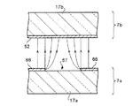
また、FPC3aの裏面すなわち配線パターン18と反対側の面には、導光体4と協働して照明装置を構成する発光素子としての複数のLED(Light Emitting Diode)21が互いに適当な間隔を開けて1列に装着すなわち実装されている。これらのLED21のための配線は、例えば、スルーホールを介して制御基板側端子16に接続される。LED21は、例えば、図7(a)に示すように、発光面24の両側に位置決め手段としてのピン26を有し、これらの発光面24及びピン26は図1において、矢印Bで示す方向、すなわちFPC3aの反対方向を向くようになっている。
【0069】
導光板4の液晶パネル2側の表面には拡散板27が貼着等によって装着され、導光板4の液晶パネル2と反対側の表面には反射板28が貼着等によって装着される。反射板28は、導光体4の光取込み面4aから取込んだ光を液晶パネル2の方向へ反射する。また、拡散板27は、導光体4から液晶パネル2へ向けて出射する光を平面的に一様な強度となるように拡散する。
【0070】
導光体4の光取込み面4aには、FPC3aに装着されたLED21の数に対応した数の収納用凹部29が設けられ、それらの収納用凹部29の両側に位置決め用凹部31が設けられる。これらの位置決め用凹部31は、FPC3aに装着されたLED21の発光面24に形成したピン26がガタツキなく挿入できる大きさ及び位置関係で形成されている。
【0071】
図2に示すように、導光体4はゴム、プラスチック等によって形成された緩衝材32を挟んで液晶パネル2の非表示面側に取り付けられる。また、制御基板5は導光体4の反射板28が装着された面に対向して配設される。この制御基板5は、液晶装置1を構成する要素として導光体4の非表示側表面に装着されることもあるし、あるいは、本液晶装置1が用いられる電子機器を構成する構成要素となる場合もある。制御基板5の辺端部には外部回路との接続をとるための端子33が形成される。
【0072】
図1に分解状態で示す液晶装置1の各構成部分を組み付ける際には、図2に示すように、FPC3aの液晶パネル2側の辺端部をACF34によって第1基板7aの張出し部分に接着する。この接着により、第1基板7aの端子13aとFPC3aの端子14とがACF34内の導電粒子によって導電接続される。その後、FPC3aは導光体4の光取込み面4aに沿って曲げられ、この曲げ状態においてFPC3aの辺端部が制御基板5の辺端部に重ねられる。そして、FPC3a側の端子16が制御基板5側の端子33に半田付け、あるいはその他の導電接続手法によって接続される。
【0073】
導電接続のためにFPC3aを上記のように曲げるとき、FPC3aの表面に装着した複数のLED21はその発光面24(図7(a)参照)が導光体4の光取込み面4aに形成した収納用凹部29に収納され、さらにLED21の発光面24に設けたピン26が位置決め用凹部31に嵌合する。以上の作業により、図2に示すように、導光体4の光取込み面4aにLED21が装着されて、液晶パネル2へ光を供給するための照明装置が構成される。図1に示すもう一方のFPC3bも同様にして、端子23を形成した辺端部が制御基板5の適所に形成した制御基板側の端子に導電接続される。
【0074】
以上により形成された液晶装置1に関して、図2において、LED21が発光すると、発光面24から出射された光が導光体4へ導入され、その導入された光が反射板28で反射して液晶パネル2の方向へ進行し、拡散板27によって平面内で一様な強度となるように拡散された状態で液晶パネル2へ供給される。供給された光は導光体側の偏向板12aを通過した成分が液晶層へ供給され、さらに画素電極66とデータ線52との間に印加される電圧の変化に応じて画素毎に配向が制御された液晶によって画素毎に変調され、さらにその変調光を表示側の偏向板12bに通すことにより、外部に像を表示する。
【0075】
以上のように本実施形態の液晶装置1では、液晶パネル2と制御基板5との間の電気的な接続を司るFPC3aによってLED21を支持するようにして、LED21を支持するための専用の基板を排除したので、LED21のための支持構造が非常に簡略化された。それ故、液晶装置のコスト低減及び小型化を達成することができた。
【0076】
また、LED21は、ピン26と凹部31との嵌合によって導光体4の光取込み面4aに対して常に一定の位置に位置決めされ、さらに、液晶装置1の使用時に導光体4に対して位置ズレすることを防止される。従って、液晶パネル2の表示の明るさが製品毎にばらつくことがなくなって、一様な表示特性の液晶装置1を安定して多数製造することができる。
【0077】
また、本実施形態では、LED21がFPC3aの液晶パネル2側の端子14と同じ面に装着され、FPC3aの配線パターン18はスルーホール19を介してその端子14に接続されることにより、LED21と反対側の面に設けられている。従って、配線パターン18はLED21に邪魔されることなく自由にパターン設計することができる。
【0078】
(第2実施形態)
図8は、本発明に係る液晶装置の他の実施形態を示している。この実施形態において、図1に示した実施形態の場合と同じ部材は同じ符号によって示すことにしてそれらについての説明は省略する。また、図8に示されていない部分の構成は図1に示した実施形態と同じである。
【0079】
本実施形態が図1に示した実施形態と異なる点は、可撓性基板としてのFPC3cに設けられる液晶パネル側端子14、制御基板側端子16及び配線パターン18の全てが、LED21が装着された面と同じ面、図8の場合には図の下面に形成されていることである。この場合には、配線パターン18とLED21を同じ個所に配置することができないので、配線パターン18はLED21を迂回するように形成される。
【0080】
(第3実施形態)
図9は、本発明に係る液晶装置のさらに他の実施形態の要部を示している。この実施形態において、図1及び図2に示した実施形態の場合と同じ部材は同じ符号によって示すことにしてそれらについての説明は省略する。また、図9に示されていない部分の構成は図1及び図2に示した実施形態と同じである。
【0081】
本実施形態が図2に示した実施形態と異なる点は、導光体4Aの光取込み面4aが液晶パネル2の反対方向へ向くような曲がり形状に形成され、FPC3aによって支持されたLED21の発光面24は、FPC3aが制御基板5の端子33に導電接続された状態で、その曲げられた光取込み面4aに対向して配置される。
【0082】
本実施形態によれば、導光体4AとFPC3aとの間に広い空間Rを形成することができ、この空間Rを、例えば、FPC3a上に実装すなわち装着したチップコンデンサその他の電子部品を収容するために用いることができるので好都合である。
【0083】
(第4実施形態)
図10は、本発明に係る液晶装置のさらに他の実施形態の要部を示している。この実施形態において、図1及び図2に示した実施形態の場合と同じ部材は同じ符号によって示すことにしてそれらについての説明は省略する。また、図10に示されていない部分の構成は図1及び図2に示した実施形態と同じである。
【0084】
本実施形態が図2に示した実施形態と異なる点は、LED21の発光面24がFPC3aへの取り付け面の側面となっており、FPC3aが制御基板5の端子33に導電接続された状態で、その側面発光面24が導光体4の光取込み面4aに対向して配置されることである。
【0085】
本実施形態によれば、導光体4とFPC3aとの間に広い空間Rを形成することができ、この空間Rを、例えば、FPC3a上に実装すなわち装着したチップコンデンサその他の電子部品を収容するために用いることができるので好都合である。
【0086】
(第5実施形態)
図7(b)は発光素子としてのLEDの変形例21Aを示している。このLED21Aは、発光点Fのまわりの発光面24が平面となっている点に関して図7(a)に示したLED21と異なっている。
【0087】
(第6実施形態)
図7(c)は発光素子としてのLEDの他の変形例21Bを示している。このLED21Bは、発光点Fのまわりの発光面24が平面となっていること及び位置決め手段としてピン26に代えて三角柱状の突起36を用いることに関して図7(a)に示したLED21と異なっている。
【0088】
(電子機器の実施形態)
図11は本発明に係る液晶装置を各種電子機器の表示装置として用いる場合の1つの実施形態を示している。ここに示す電子機器は、表示情報出力源100、表示情報処理回路101、電源回路102、タイミングジェネレータ103、そして液晶装置104を有する。また、液晶装置104は液晶パネル105及び駆動回路106を有する。液晶装置104は図1に示した液晶装置1を用いることができ、液晶パネル105は図1に示した液晶パネル2を用いることができる。
【0089】
表示情報出力源100は、ROM(Read Only Memory)、RAM(Random Access Memory)等といったメモリ、各種ディスク等といったストレージユニット、デジタル画像信号を同調出力する同調回路等を備え、タイミングジェネレータ103によって生成された各種のクロック信号に基づいて、所定フォーマットの画像信号等といった表示情報を表示情報処理回路101に供給する。
【0090】
表示情報処理回路101は、シリアル−パラレル変換回路や、増幅・反転回路、ローテーション回路、ガンマ補正回路、クランプ回路等といった周知の各種回路を備え、入力した表示情報の処理を実行して、その画像信号をクロック信号CLKと共に駆動回路106へ供給する。駆動回路106は、図3における走査線駆動回路57やデータ線駆動回路58、検査回路等を総称したものである。また、電源回路102は、各構成要素に所定の電源を供給する。
【0091】
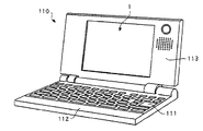
図12は本発明に係る電子機器の一実施形態であるモバイル型のパーソナルコンピュータを示している。ここに示すパーソナルコンピュータ110は、キーボード111を備えた本体部112と、液晶表示ユニット113とを有する。液晶表示ユニット113は、図1に示す液晶装置1を含んで構成される。図13は本発明に係る電子機器の他の一実施形態である携帯電話機を示している。ここに示す携帯電話機120は、複数の操作ボタン121と、液晶装置1とを有する。
【0092】
図12及び図13の実施形態で用いられる液晶装置1は、図1に関連して説明したように半透過半反射型の液晶装置であるので、コンピュータや携帯電話機が外光の不十分な場所に置かれた場合でも、LED21及び導光体4によって構成される照明装置、いわゆるバックライトを点灯させることにより、何等の支障もなく表示を視認できる。
【0093】
また、図1の液晶装置1では、液晶パネル2と制御基板5との間の電気的な接続を司るFPC3aによってLED21を支持するようにして、LED21を支持するための専用の基板を排除したので、LED21のための支持構造が非常に簡略化された。それ故、液晶装置1を小型に形成することが可能となり、図12においてこの液晶装置1を液晶表示ユニット113へ組み込むことにより、液晶表示ユニット113の枠部分、いわゆる額縁領域を狭く形成することが可能となった。また、図13の携帯電話機120に関して言えば、液晶装置1の小型化により、携帯電話機の外形を小さくした場合でも大きな表示部を組み込むことができるようになった。
【0094】
また、図2において、LED21はピン26と凹部31との嵌合によって導光体4の光取込み面4aに対して常に一定の位置に位置決めされ、さらに、液晶装置1の使用時に導光体4に対して位置ズレすることを防止されるので、液晶パネル2の表示の明るさが製品毎にばらつくことがなくなった。このため、図12のコンピュータの表示画面の明るさ及び図13の携帯電話機120の表示画面の明るさも製品毎にばらつきのない、一様な表示特性が得られるようになった。
【0095】
(その他の実施形態)
以上、好ましい実施形態を挙げて本発明を説明したが、本発明はその実施形態に限定されるものでなく、請求の範囲に記載した発明の範囲内で種々に改変できる。
【0096】
例えば、図1に示す実施形態では半透過半反射型でTFDを用いたアクティブマトリクス方式の液晶装置に本発明を適用したが、本発明はその他各種の方式の液晶装置、例えば反射型の液晶装置、透過型の液晶装置、TFD以外のスイッチング素子を用いたアクティブマトリクス方式の液晶装置、スイッチング素子を用いないパッシブマトリクス方式の液晶装置等に対して適用することもできる。
【0097】
【発明の効果】
以上に説明したように、本発明に係る液晶装置によれば、液晶を挟持する基板に接続される可撓性基板の上に発光素子が取り付けられ、この可撓性基板は液晶に対する何等かの電気的な配線のために用いられるものであって、発光素子を導光体に装着するための専用の基板ではないので、発光素子の支持構造が非常に簡略化され、それ故、液晶装置のコスト低減及び小型化を達成することができる。
【図面の簡単な説明】
【図1】本発明に係る液晶装置の一実施形態を分解状態で示す斜視図である。
【図2】図1に示す液晶装置の断面構造を示す断面図である。
【図3】図1に示す液晶装置を構成する液晶パネルの電気的構成を模式的に示す図である。
【図4】図3の液晶パネルにおける1画素分の構造を示す図であり、(a)は平面図であり、(b)は(a)のA−A線に従った断面図である。
【図5】素子基板における電界方向を示す断面図である。
【図6】素子基板における電界強度と液晶分子の配列との関係を模式的に示す図である。
【図7】発光素子のいくつかの実施形態を示す斜視図である。
【図8】本発明に係る液晶装置の他の実施形態を分解状態で示す斜視図である。
【図9】本発明に係る液晶装置のさらに他の実施形態の要部を示す断面図である。
【図10】本発明に係る液晶装置のさらに他の実施形態の要部を示す断面図である。
【図11】本発明に係る電子機器の表示制御系の一実施形態を示すブロック図である。
【図12】本発明に係る電子機器の一実施形態を示す斜視図である。
【図13】本発明に係る電子機器の他の実施形態を示す斜視図である。
【符号の説明】
1 液晶装置
2 液晶パネル
3a FPC(可撓性基板)
4 導光体
5 制御基板
7a 第1基板(素子基板)
7b 第2基板(対向基板)
8a,8b 液晶駆動用IC
9 ACF
13a,13b 端子
14 端子
16 端子
17a,17b 基台
18 配線パターン
19 スルーホール
21 LED(発光素子)
26 ピン(位置決め手段)
29 収納用凹部
31 位置決め用凹部(位置決め手段)
33 端子
36 三角柱状突起(位置決め手段)
F 発光点
L 液晶
M 液晶分子
R 空間
W スリット幅[0001]
BACKGROUND OF THE INVENTION
The present invention relates to a liquid crystal device that displays an image by modulating the light passing through the liquid crystal by controlling the alignment of the liquid crystal. The present invention also relates to an electronic apparatus using the liquid crystal device.
[0002]
[Prior art]
In recent years, liquid crystal devices are widely used in electronic devices such as computers and mobile phones. In this liquid crystal device, generally, a liquid crystal is sandwiched between a pair of substrates provided with electrodes, and a voltage is applied between the electrodes to control the orientation of the liquid crystal, thereby modulating light passing through the liquid crystal and displaying an image. I do.
[0003]
Differentiating liquid crystal devices based on the way light is supplied to the liquid crystal, a reflective liquid crystal device that reflects external light by a reflector provided on the outer surface or inner surface of one substrate, or provided outside the one substrate A transflective liquid crystal device with a structure that supplies light to the liquid crystal in a planar manner by a lighting device or a transflective device that functions as a reflective type when there is external light and as a transmissive type when external light is insufficient Various liquid crystal devices such as a semi-reflective liquid crystal device are known.
[0004]
Conventionally, a light emitting element such as an LED (Light Emitting Diode) is used as a light emitting source as a liquid crystal device that supplies light to liquid crystal using an illumination device such as a transmissive liquid crystal device or a transflective liquid crystal device. Structures are known. In this type of liquid crystal device, the light emitting element is usually mounted on a non-flexible substrate such as a glass epoxy substrate, and the non-flexible substrate is mounted on the housing of the light guide so that the light emitting element is guided to the light guide. It is arranged opposite to the light intake surface.
[0005]
[Problems to be solved by the invention]
However, in the conventional liquid crystal device having the above-described structure, a dedicated inflexible substrate for the light emitting element must be used and a structure for supporting the inflexible substrate must be constructed. However, the structure is complicated and the liquid crystal device cannot be downsized.
[0006]
The present invention has been made in view of the above problems, and a first object thereof is to achieve cost reduction and miniaturization of a liquid crystal device by simplifying a support structure of a light emitting element.
[0007]
In addition, even when the support structure of the light emitting element is simplified, the present invention prevents variations in the light incident efficiency to the light guide by preventing the relative position of the light emitting element with respect to the light guide. The second object is to prevent the occurrence of variations in the light supplied to the liquid crystal.
[0008]
(1) In order to achieve the first object, a first liquid crystal device according to the present invention includes a pair of substrates that sandwich a liquid crystal, a light guide provided to face one of the pair of substrates, In the liquid crystal device having a flexible substrate connected to one of the pair of substrates and a light emitting element provided to face the light capturing surface of the light guide, the light emitting element is the flexible substrate. It is desirable that the light guide is mounted at a position facing the light capturing surface of the light guide.
[0009]
In this liquid crystal device, a light emitting element is mounted on a flexible substrate (FPC: Flexible Printed Circuit) connected to a substrate that sandwiches liquid crystal. This flexible substrate is used for any electrical wiring with respect to the liquid crystal, and is not a dedicated substrate for mounting the light emitting element on the light guide. Therefore, according to the present invention, the support structure of the light emitting element can be greatly simplified, and thus the cost reduction and size reduction of the liquid crystal device can be achieved.
[0010]
In the liquid crystal device according to the first aspect of the present invention, the light emitting element is disposed to face the light capturing surface by bending the flexible substrate along the light capturing surface of the light guide. desirable. In many cases, a control board for controlling the operation of the liquid crystal sandwiched between the pair of substrates is provided separately from the pair of substrates. In many cases, the flexible substrate is bent along the light capturing surface of the light guide and then connected to the control substrate. Therefore, it is preferable that the light emitting element is disposed at a position facing the light capturing surface when the flexible substrate is bent along the light capturing surface of the light guide.
[0011]
In the liquid crystal device according to the first aspect, the flexible substrate has a terminal connected to the substrate, and the light emitting element is provided on the same flexible substrate surface as the surface on which the terminal is provided. Furthermore, it is preferable that the flexible substrate has a wiring pattern on a surface opposite to the surface on which the light emitting element is provided, and the wiring pattern and the terminal are connected by a through hole. According to this configuration, since there is no wiring pattern on the surface of the flexible substrate to which the light emitting element is attached, the position where the light emitting element is attached can be freely selected, which is preferable. In addition, since the wiring pattern is not obstructed by the light emitting element, the pattern design becomes easy.
[0012]
Further, in the liquid crystal device according to the first invention, the flexible substrate has a terminal connected to the substrate, has a wiring pattern on the same surface as the surface on which the terminal is provided, and the light emitting element It is also possible to provide it on the same flexible substrate surface as the surface on which the wiring pattern is provided.
[0013]
Further, in the liquid crystal device of the present invention having the structure in which the light emitting element is provided on the same flexible substrate surface as the surface on which the wiring pattern is provided, the wiring pattern avoids the light emitting element on the flexible substrate. It is desirable to be provided. In this way, even when the light emitting element is attached on the flexible substrate, it is possible to prevent the wiring pattern from being hindered.
[0014]
In the liquid crystal device according to the first aspect of the present invention, the light emitting element can be attached to the flexible substrate such that the side surface of the surface attached to the flexible substrate becomes the light emitting surface. The light emitting surface which is the side surface is disposed to face the light capturing surface of the light guide. According to this configuration, as shown in FIG. 10, a wide space R can be formed on the opposite side of the light emitting surface of the light emitting element, and this space R can be used to accommodate, for example, chip capacitors and other electronic components. Can be used.
[0015]
In the liquid crystal device according to the first aspect of the present invention, the light guide body can be formed in a bent shape such that the light taking surface faces in the opposite direction of the pair of substrates, and the light emitting surface of the light emitting element is a pair of light emitting surfaces. It can be arranged opposite to the light capture surface directed in the opposite direction of the substrate. According to this configuration, as shown in FIG. 9, a wide space R can be formed between the light guide and the flexible substrate, and this space R can accommodate, for example, chip capacitors and other electronic components. Can be used to
[0016]
In the liquid crystal device according to the first aspect of the present invention, the flexible substrate is not limited to being used for a specific application, but preferably for supplying a signal for driving the liquid crystal. It is a substrate.
[0017]
(2) Next, in order to achieve the second object, a liquid crystal device according to the present invention includes a pair of substrates that sandwich the liquid crystal, a light guide provided to face one of the pair of substrates, A flexible substrate connected to one of the pair of substrates and bent to the back side of the pair of substrates, and an inner side of the flexible substrate mounted and bent on the flexible substrate And disposed opposite to the light capturing surface of the light guide, and provided at a portion other than the light emitting point and the portion where the light emitting point and the light capturing surface of the light guide plate are opposed to each other. A light-emitting element having a positioning convex portion, and a light-receiving surface of the light guide has a positioning concave portion, and when the flexible substrate is bent, the positioning concave portion and the light-emitting element The positioning convex part is fitted, and the light guide and the light emitting element are positioned. It is characterized by being arranged. The liquid crystal device according to the present invention is characterized in that the positioning convex portion is a cylindrical pin or a triangular projection.
The second liquid crystal device according to the present invention includes a pair of substrates that sandwich the liquid crystal, a light guide that is provided to face one of the pair of substrates, and can be connected to any one of the pair of substrates. In a liquid crystal device having a flexible substrate and a light emitting element provided opposite to the light capturing surface of the light guide, the light emitting element is mounted on the flexible substrate, and is disposed on the light capturing surface. It is desirable that a positioning means for positioning the light emitting element is provided between the light emitting element and the light receiving surface of the light guide.
[0018]
The difference between the liquid crystal device according to the second aspect of the invention and the first liquid crystal device is that the light emitting element is provided on a flexible substrate and is disposed at a position facing the light receiving surface of the light guide. In addition, a positioning means for positioning the light emitting element is provided between the light emitting element and the light capturing surface of the light guide.
[0019]
According to the liquid crystal device according to the second aspect of the invention, since the light emitting element is disposed on the flexible substrate at a position facing the light receiving surface of the light guide, the light emitting element support structure is provided. Can be greatly simplified, and therefore, cost reduction and downsizing of the liquid crystal device can be achieved.
[0020]
Moreover, even when the support structure of the light emitting element is simplified as described above, the relative position of the light emitting element with respect to the light guide can be prevented by the action of the positioning means. For this reason, it is possible to prevent variation in the incidence efficiency of light to the light guide, and as a result, it is possible to prevent variation in the light supplied to the liquid crystal.
[0021]
In the liquid crystal device according to the second aspect of the present invention, the positioning means is provided on a convex portion provided on one side of the light emitting element side or the light guide body side and on the other side of the light emitting element side or the light guide body side. It is desirable to have the recessed part which the said convex part fits. The convex portion may be a cylindrical pin or a triangular protrusion.
[0022]
In the liquid crystal device according to the second aspect of the invention, it is preferable that the light emitting element is disposed to face the light capturing surface by bending the flexible substrate along the light capturing surface of the light guide. In many cases, a control board for controlling the operation of the liquid crystal sandwiched between the pair of substrates is provided separately from the pair of substrates. In many cases, the flexible substrate is bent along the light capturing surface of the light guide and then connected to the control substrate. Therefore, it is preferable that the light emitting element is disposed at a position facing the light capturing surface when the flexible substrate is bent along the light capturing surface of the light guide.
[0023]
In the liquid crystal device according to the second invention, the flexible substrate has a terminal connected to the substrate, and the light emitting element is provided on the same flexible substrate surface as the surface on which the terminal is provided. Furthermore, it is preferable that the flexible substrate has a wiring pattern on a surface opposite to the surface on which the light emitting element is provided, and the wiring pattern and the terminal are connected by a through hole.
[0024]
According to this configuration, since there is no wiring pattern on the surface of the flexible substrate to which the light emitting element is attached, the position where the light emitting element is attached can be freely selected, which is preferable. In addition, since the wiring pattern is not obstructed by the light emitting element, the pattern design becomes easy.
[0025]
In the liquid crystal device according to a second aspect of the present invention, the flexible substrate has a terminal connected to the substrate, has a wiring pattern on the same surface as the surface on which the terminal is provided, and the light emitting element It is also possible to provide it on the same flexible substrate surface as the surface on which the wiring pattern is provided.
[0026]
In the liquid crystal device according to a second aspect of the invention, the light emitting element is provided on the same flexible substrate surface as the surface on which the wiring pattern is provided. The wiring pattern is formed on the flexible substrate on the light emitting element. It is desirable to avoid this. In this way, even when the light emitting element is attached on the flexible substrate, it is possible to prevent the wiring pattern from being hindered.
[0027]
Further, in the liquid crystal device according to the second invention, the light emitting element can be attached to the flexible substrate so that a side surface of the surface attached to the flexible substrate becomes a light emitting surface. The light emitting surface which is the side surface is disposed to face the light capturing surface of the light guide. According to this configuration, as shown in FIG. 10, a wide space R can be formed on the opposite side of the light emitting surface of the light emitting element, and this space R can be used to accommodate, for example, chip capacitors and other electronic components. Can be used.
[0028]
In the liquid crystal device according to a second aspect of the present invention, the light guide can be formed in a bent shape such that the light taking surface thereof faces in the opposite direction of the pair of substrates, and the light emitting surface of the light emitting element is a pair of light emitting surfaces. It can be arranged opposite to the light capture surface directed in the opposite direction of the substrate. According to this configuration, as shown in FIG. 9, a wide space R can be formed between the light guide and the flexible substrate, and this space R can accommodate, for example, chip capacitors and other electronic components. Can be used to
[0029]
In the liquid crystal device according to the second aspect of the present invention, the flexible substrate is not limited to being used for a specific application, but preferably for supplying a signal for driving the liquid crystal. It is a substrate.
[0030]
(3) Next, an electronic apparatus according to the present invention is an electronic apparatus having a liquid crystal device and a control circuit for controlling the operation of the liquid crystal device, wherein the liquid crystal device is the liquid crystal device according to the first invention or the above-described liquid crystal device. It is comprised by the liquid crystal device which concerns on 2nd invention, The said flexible substrate is connected to the said control circuit, The said light emitting element is arrange | positioned facing the light-entrance surface of the said light guide in the connection state. Features.
[0031]
According to this electronic apparatus, when the liquid crystal device according to the first invention is used, the structure around the light emitting element used as the illumination light source in the liquid crystal device is greatly simplified and miniaturized. It becomes easy to design the structure of the equipment.
[0032]
Further, when the liquid crystal device according to the second invention is used, it is determined that the relative position of the light emitting element with respect to the light guide is shifted even when the structure around the light emitting element is simplified as described above. Since it can be prevented by the action of the means, it is possible to prevent variation in the incidence efficiency of light to the light guide, and therefore it is possible to prevent variation in the light supplied to the liquid crystal. As a result, it is possible to reliably prevent variations in the brightness of the image displayed on the display unit configured by the liquid crystal device for each product of the manufactured electronic device, and to provide a certain display quality. Can be manufactured stably.
[0033]
DETAILED DESCRIPTION OF THE INVENTION
When the liquid crystal device is distinguished by the liquid crystal driving method, the active matrix type liquid crystal device in which the pixel electrode is driven by a switching element (that is, a non-linear element), and a passive that includes a simple matrix arrangement that does not use the switching element. A matrix type liquid crystal device can be considered. Comparing the two, it is considered that the active matrix method is more advantageous in that the contrast and response are good and high-definition display can be easily achieved.
[0034]
In addition, as an active matrix liquid crystal device, a method using a three-terminal element such as a thin film transistor (TFT) as a switching element and a two-terminal element such as a thin film diode (TFD) are used. The method is known. Among these, a liquid crystal device using TFD or the like has advantages such as no short circuit failure between wirings due to the absence of wiring intersections, and shortening of a film forming process and a photolithography process. Yes.
[0035]
Hereinafter, embodiments of the present invention will be described by taking as an example the case where the first invention and the second invention described above are applied to an active matrix liquid crystal device having a structure using TFD as a switching element for a pixel electrode. The liquid crystal device according to the present embodiment is a transflective liquid crystal device that functions as a reflection type when there is external light and functions as a transmission type when external light is insufficient. .
[0036]
FIG. 1 shows a liquid crystal device 1 according to the embodiment. In the liquid crystal device 1, an FPC (Flexible Printed Circuit) 3 a and an
[0037]
The
[0038]
The liquid crystal device of the present embodiment is an active matrix type liquid crystal device using TFD as a switching element, and one of the
[0039]
As shown in FIG. 2, the
[0040]
Although not shown in FIG. 2, various optical elements other than the above are provided on the
[0041]
In the case of performing color display, R (red), G (green), and B (blue) primary color filters are provided on a portion of the counter substrate facing the pixel electrode formed on the element substrate. A black matrix of Bk (black) is formed in a region which is formed in an array and does not face the pixel electrode. Furthermore, a smoothing layer is coated for smoothing and protecting the surface of the color filter and black matrix. The counter electrode provided on the counter substrate side is formed on the smoothing layer.
[0042]
FIG. 3 schematically shows the electrical configuration of the
[0043]
Each
[0044]
In FIG. 3, the
[0045]
The
[0046]
Next, FIG. 4 shows a configuration for one pixel in the
[0047]
The
[0048]
A preferable value for the thickness of the
[0049]
The
[0050]
Here, the
[0051]
The
[0052]
By the way, the
[0053]
The insulating
[0054]
The
[0055]
In FIG. 4, the
[0056]
Now, the liquid crystal panel 2 (see FIG. 1) is pasted in a state where the
In other words, the rubbing direction that determines the orientation direction of the liquid crystal molecules when no voltage is applied is seen diagonally upward to the left in the
[0057]
The rubbing process is generally performed by rubbing a buff cloth wound around a roller in a certain direction, so that undesirable situations such as generation of static electricity and generation of various dusts are likely to occur. In the present embodiment, since the buff cloth travels in the rubbing process in the same direction as the slit direction of the
[0058]
In the above description, the
[0059]
By the way, the direction of the electric field generated by the
[0060]
On the other hand, since the rubbing direction of the
[0061]
As described above, it is desirable that the slit direction and the rubbing direction of the
[0062]
When the rubbing direction and the slit direction of the
[0063]
Next, the width and area of the
[0064]
If the width W of the
[0065]
Returning to FIG. 1, a plurality of
[0066]
The
[0067]
On the other hand, with respect to the
[0068]
In addition, on the back surface of the
[0069]
A
[0070]
The
[0071]
As shown in FIG. 2, the
[0072]
When assembling each component of the liquid crystal device 1 shown in an exploded state in FIG. 1, the side edge of the
[0073]
When the
[0074]
With respect to the liquid crystal device 1 formed as described above, in FIG. 2, when the
[0075]
As described above, in the liquid crystal device 1 according to the present embodiment, the
[0076]
Further, the
[0077]
Further, in this embodiment, the
[0078]
(Second Embodiment)
FIG. 8 shows another embodiment of the liquid crystal device according to the present invention. In this embodiment, the same members as those in the embodiment shown in FIG. 1 are denoted by the same reference numerals, and description thereof will be omitted. Moreover, the structure of the part which is not shown by FIG. 8 is the same as embodiment shown in FIG.
[0079]
This embodiment is different from the embodiment shown in FIG. 1 in that all of the liquid crystal
[0080]
(Third embodiment)
FIG. 9 shows a main part of still another embodiment of the liquid crystal device according to the present invention. In this embodiment, the same members as those in the embodiment shown in FIGS. 1 and 2 are denoted by the same reference numerals, and description thereof will be omitted. Further, the configuration of the part not shown in FIG. 9 is the same as that of the embodiment shown in FIGS.
[0081]
The difference between the present embodiment and the embodiment shown in FIG. 2 is that the light-receiving
[0082]
According to this embodiment, a wide space R can be formed between the
[0083]
(Fourth embodiment)
FIG. 10 shows a main part of still another embodiment of the liquid crystal device according to the present invention. In this embodiment, the same members as those in the embodiment shown in FIGS. 1 and 2 are denoted by the same reference numerals, and description thereof will be omitted. Further, the configuration of the portion not shown in FIG. 10 is the same as that of the embodiment shown in FIGS.
[0084]
The present embodiment is different from the embodiment shown in FIG. 2 in that the
[0085]
According to the present embodiment, a wide space R can be formed between the
[0086]
(Fifth embodiment)
FIG. 7B shows a
[0087]
(Sixth embodiment)
FIG.7 (c) has shown
[0088]
(Embodiment of electronic device)
FIG. 11 shows an embodiment in which the liquid crystal device according to the present invention is used as a display device of various electronic devices. The electronic device shown here includes a display
[0089]
The display
[0090]
The display
[0091]
FIG. 12 shows a mobile personal computer which is an embodiment of an electronic apparatus according to the present invention. The
[0092]
Since the liquid crystal device 1 used in the embodiment of FIGS. 12 and 13 is a transflective liquid crystal device as described with reference to FIG. 1, the computer or the cellular phone is a place where the external light is insufficient. Even if it is placed on, the display can be visually recognized without any trouble by turning on the lighting device constituted by the
[0093]
Further, in the liquid crystal device 1 of FIG. 1, the
[0094]
In FIG. 2, the
[0095]
(Other embodiments)
The present invention has been described with reference to the preferred embodiments. However, the present invention is not limited to the embodiments, and various modifications can be made within the scope of the invention described in the claims.
[0096]
For example, in the embodiment shown in FIG. 1, the present invention is applied to an active matrix type liquid crystal device using a transflective type and a TFD. However, the present invention is applicable to various types of liquid crystal devices such as a reflective type liquid crystal device. The present invention can also be applied to transmissive liquid crystal devices, active matrix liquid crystal devices using switching elements other than TFD, passive matrix liquid crystal devices that do not use switching elements, and the like.
[0097]
【The invention's effect】
As described above, according to the liquid crystal device according to the present invention, the light emitting element is mounted on the flexible substrate connected to the substrate that sandwiches the liquid crystal. Since it is used for electrical wiring and is not a dedicated substrate for mounting the light emitting element on the light guide, the support structure of the light emitting element is greatly simplified. Cost reduction and miniaturization can be achieved.
[Brief description of the drawings]
FIG. 1 is a perspective view showing an embodiment of a liquid crystal device according to the present invention in an exploded state.
2 is a cross-sectional view showing a cross-sectional structure of the liquid crystal device shown in FIG.
3 is a diagram schematically showing an electrical configuration of a liquid crystal panel constituting the liquid crystal device shown in FIG. 1. FIG.
4A and 4B are diagrams illustrating the structure of one pixel in the liquid crystal panel of FIG. 3, in which FIG. 4A is a plan view, and FIG. 4B is a cross-sectional view taken along line AA in FIG.
FIG. 5 is a cross-sectional view showing an electric field direction in an element substrate.
FIG. 6 is a diagram schematically showing the relationship between the electric field strength and the arrangement of liquid crystal molecules in the element substrate.
FIG. 7 is a perspective view showing some embodiments of a light emitting device.
FIG. 8 is a perspective view showing another embodiment of the liquid crystal device according to the present invention in an exploded state.
FIG. 9 is a cross-sectional view showing a main part of still another embodiment of the liquid crystal device according to the present invention.
FIG. 10 is a cross-sectional view showing a main part of still another embodiment of the liquid crystal device according to the present invention.
FIG. 11 is a block diagram showing an embodiment of a display control system of an electronic device according to the present invention.
FIG. 12 is a perspective view showing an embodiment of an electronic apparatus according to the invention.
FIG. 13 is a perspective view showing another embodiment of an electronic apparatus according to the invention.
[Explanation of symbols]
1 Liquid crystal device
2 LCD panel
3a FPC (flexible substrate)
4 Light guide
5 Control board
7a First substrate (element substrate)
7b Second substrate (counter substrate)
8a, 8b Liquid crystal drive IC
9 ACF
13a, 13b terminal
14 terminals
16 terminals
17a, 17b base
18 Wiring pattern
19 Through hole
21 LED (light emitting device)
26 pins (positioning means)
29 Recess for storage
31 Recess for positioning (positioning means)
33 terminals
36 Triangular prismatic protrusion (positioning means)
F luminous point
L liquid crystal
M liquid crystal molecules
R space
W Slit width
Claims (10)
前記一対の基板の一方に対向して設けられる導光体と、
前記一対の基板のいずれか一方に接続され、前記一対の基板の背面側に折り曲げられてなる可撓性基板と、
前記可撓性基板上に実装され、折り曲げられた前記可撓性基板の内側に配置されてなるとともに、前記導光体の光取込み面に対向して配置されてなり、発光点と、当該発光点と前記導光板の光取り込み面とが対向する箇所以外の部分に設けられてなる位置決め用凸部と、を有する発光素子と、を有し、
前記導光体の光取込み面は、位置決め用凹部を有し、
前記可撓性基板を折り曲げるときに前記位置決め用凹部と前記位置決め用凸部が嵌合し、前記導光体と前記発光素子が位置決めされてなることを特徴とする液晶装置。A pair of substrates sandwiching the liquid crystal;
A light guide provided to face one of the pair of substrates;
A flexible substrate connected to either one of the pair of substrates and bent to the back side of the pair of substrates;
Mounted on the flexible substrate and disposed inside the bent flexible substrate, and disposed to face the light capturing surface of the light guide, and the light emitting point and the light emission A light emitting element having a positioning convex portion provided at a portion other than a portion where the point and the light capturing surface of the light guide plate face each other, and
The light capturing surface of the light guide has a positioning recess,
The liquid crystal device, wherein the positioning concave portion and the positioning convex portion are fitted when the flexible substrate is bent, and the light guide and the light emitting element are positioned.
Priority Applications (8)
| Application Number | Priority Date | Filing Date | Title |
|---|---|---|---|
| JP2000151666A JP3642263B2 (en) | 2000-05-23 | 2000-05-23 | Liquid crystal device and electronic device |
| TW090110645A TWI291064B (en) | 2000-05-23 | 2001-05-03 | Liquid crystal device and electronic device |
| KR10-2001-0027607A KR100441327B1 (en) | 2000-05-23 | 2001-05-21 | Liquid crystal device and electronic device |
| US09/863,059 US6897912B2 (en) | 2000-05-23 | 2001-05-22 | Liquid crystal device and electronic device |
| AT01304507T ATE335219T1 (en) | 2000-05-23 | 2001-05-22 | LIQUID CRYSTAL DEVICE AND ELECTRONIC DEVICE |
| EP01304507A EP1158347B1 (en) | 2000-05-23 | 2001-05-22 | Liquid crystal device and electronic device |
| CNB011195010A CN1208667C (en) | 2000-05-23 | 2001-05-22 | Liquid crystal device and electronic apparatus |
| DE60121858T DE60121858T2 (en) | 2000-05-23 | 2001-05-22 | Liquid crystal device and electronic device |
Applications Claiming Priority (1)
| Application Number | Priority Date | Filing Date | Title |
|---|---|---|---|
| JP2000151666A JP3642263B2 (en) | 2000-05-23 | 2000-05-23 | Liquid crystal device and electronic device |
Publications (3)
| Publication Number | Publication Date |
|---|---|
| JP2001330830A JP2001330830A (en) | 2001-11-30 |
| JP2001330830A5 JP2001330830A5 (en) | 2005-03-03 |
| JP3642263B2 true JP3642263B2 (en) | 2005-04-27 |
Family
ID=18657187
Family Applications (1)
| Application Number | Title | Priority Date | Filing Date |
|---|---|---|---|
| JP2000151666A Expired - Lifetime JP3642263B2 (en) | 2000-05-23 | 2000-05-23 | Liquid crystal device and electronic device |
Country Status (8)
| Country | Link |
|---|---|
| US (1) | US6897912B2 (en) |
| EP (1) | EP1158347B1 (en) |
| JP (1) | JP3642263B2 (en) |
| KR (1) | KR100441327B1 (en) |
| CN (1) | CN1208667C (en) |
| AT (1) | ATE335219T1 (en) |
| DE (1) | DE60121858T2 (en) |
| TW (1) | TWI291064B (en) |
Families Citing this family (48)
| Publication number | Priority date | Publication date | Assignee | Title |
|---|---|---|---|---|
| US6697130B2 (en) * | 2001-01-16 | 2004-02-24 | Visteon Global Technologies, Inc. | Flexible led backlighting circuit |
| JP4689851B2 (en) * | 2001-02-23 | 2011-05-25 | Nec液晶テクノロジー株式会社 | Active matrix liquid crystal display device |
| EP1376212A1 (en) * | 2002-06-21 | 2004-01-02 | Asulab S.A. | Display cell, in particular comprising liquid crystals, or photovoltaic cell comprising connection means to a driver circuit |
| JP2004247373A (en) | 2003-02-12 | 2004-09-02 | Semiconductor Energy Lab Co Ltd | Semiconductor device |
| JP4217090B2 (en) * | 2003-03-20 | 2009-01-28 | 株式会社 日立ディスプレイズ | Display device |
| KR20040087464A (en) * | 2003-04-08 | 2004-10-14 | 삼성전자주식회사 | Liquid crystal display device |
| TW594176B (en) * | 2003-06-17 | 2004-06-21 | Au Optronics Corp | Circuit scheme of light emitting device and liquid crystal display |
| JP2005070569A (en) | 2003-08-27 | 2005-03-17 | Nec Corp | Mobile communication machine and liquid crystal display module mounting method used therefor |
| JP4543772B2 (en) * | 2003-09-19 | 2010-09-15 | セイコーエプソン株式会社 | Electro-optical device and electronic apparatus |
| JP4072493B2 (en) * | 2003-11-14 | 2008-04-09 | Nec液晶テクノロジー株式会社 | Substrate module and liquid crystal module |
| US7196693B2 (en) * | 2003-12-12 | 2007-03-27 | Compal Electronics, Inc. | Lighting keyboard and lighting module thereof |
| JP4055741B2 (en) | 2004-05-24 | 2008-03-05 | セイコーエプソン株式会社 | Electro-optical device and electronic apparatus |
| JP4072519B2 (en) * | 2004-06-18 | 2008-04-09 | シャープ株式会社 | Lighting device for display device |
| JP4581726B2 (en) * | 2004-12-28 | 2010-11-17 | ソニー株式会社 | Display device and portable device |
| TWM272351U (en) * | 2005-01-21 | 2005-08-01 | Innolux Display Corp | Display module |
| JP4244942B2 (en) | 2005-03-08 | 2009-03-25 | セイコーエプソン株式会社 | Liquid crystal device, lighting device, and electronic device |
| US7284894B2 (en) * | 2005-05-31 | 2007-10-23 | Avago Technologies Eceliip (Singapore) Pte Ltd | Light source utilizing a flexible circuit carrier |
| TW200712684A (en) * | 2005-09-30 | 2007-04-01 | Innolux Display Corp | Liquid crystal display module |
| CN1971345B (en) * | 2005-11-24 | 2010-05-12 | 群康科技(深圳)有限公司 | Flexible circuit board and LCD device |
| US8189133B2 (en) * | 2006-02-10 | 2012-05-29 | Nokia Corporation | Display module and method for fixing |
| TWI326375B (en) | 2006-04-21 | 2010-06-21 | Chimei Innolux Corp | Liquid crystal display device |
| CN100368895C (en) * | 2006-05-30 | 2008-02-13 | 友达光电股份有限公司 | Backlight module using LED |
| KR100786479B1 (en) | 2006-09-22 | 2007-12-17 | 삼성에스디아이 주식회사 | Flat panel display device and portable display appratus using the same |
| KR100821042B1 (en) * | 2006-09-22 | 2008-04-08 | 삼성에스디아이 주식회사 | Liquid Crystal Display Device and Portable Display Appratus using the same |
| KR100821043B1 (en) * | 2006-09-22 | 2008-04-08 | 삼성에스디아이 주식회사 | Flexilble Printed Circuit Board |
| KR101284053B1 (en) | 2006-10-26 | 2013-07-10 | 삼성디스플레이 주식회사 | Back-light assembly and display apparatus having the same |
| JP4333727B2 (en) * | 2006-11-13 | 2009-09-16 | エプソンイメージングデバイス株式会社 | ELECTRO-OPTICAL DEVICE, LIGHTING DEVICE, AND ELECTRONIC DEVICE |
| JP5010925B2 (en) * | 2007-01-12 | 2012-08-29 | 株式会社ジャパンディスプレイイースト | LCD module |
| CN101611262B (en) * | 2007-02-16 | 2011-01-26 | 夏普株式会社 | Backlight device and planar display device using the same |
| TWI330415B (en) * | 2007-04-02 | 2010-09-11 | Chimei Innolux Corp | Light emitting diode and a backlight module using the same |
| CN101281942B (en) * | 2007-04-06 | 2011-06-29 | 群康科技(深圳)有限公司 | LED and backlight module using the same |
| KR100857693B1 (en) | 2007-05-10 | 2008-09-08 | 삼성에스디아이 주식회사 | Liquid crystal display device |
| US7707974B2 (en) * | 2007-07-25 | 2010-05-04 | Radio Systems Corporation | LCD window for animal training device and method for manufacture |
| TWM329818U (en) * | 2007-10-17 | 2008-04-01 | Universal Scient Ind Co Ltd | Portable electronic device with anisotropic conductive unit |
| KR101431154B1 (en) * | 2007-11-08 | 2014-08-18 | 삼성디스플레이 주식회사 | Display apparatus and method for assembling the same |
| EP2299316B1 (en) | 2008-07-08 | 2013-03-13 | Sharp Kabushiki Kaisha | Liquid crystal display device |
| WO2012157547A1 (en) * | 2011-05-18 | 2012-11-22 | シャープ株式会社 | Display device |
| TWI553382B (en) | 2011-06-24 | 2016-10-11 | Lg伊諾特股份有限公司 | Illumination system |
| KR101307960B1 (en) * | 2012-04-26 | 2013-09-12 | 엘지디스플레이 주식회사 | Display device |
| KR101346083B1 (en) * | 2012-04-26 | 2013-12-31 | 엘지디스플레이 주식회사 | Display Device |
| CN102809100A (en) * | 2012-08-09 | 2012-12-05 | 京东方科技集团股份有限公司 | Backlight and production method thereof |
| US9072167B2 (en) * | 2012-08-27 | 2015-06-30 | Shenzhen China Star Optoelectronics Technology Co., Ltd. | Display device |
| US8988875B2 (en) * | 2012-08-27 | 2015-03-24 | Shenzhen China Star Optoelectronics Technology Co., Ltd. | Display device |
| US9084338B2 (en) * | 2012-08-27 | 2015-07-14 | Shenzhen China Star Optoelectronics Technology Co., Ltd. | Display device |
| US8988866B2 (en) * | 2012-08-27 | 2015-03-24 | Shenzhen China Star Optoelectronics Technology Co., Ltd. | Display device |
| KR102416142B1 (en) * | 2015-08-31 | 2022-07-01 | 엘지디스플레이 주식회사 | Back cover and transparent display apparatus using the same |
| CN108398818B (en) * | 2017-02-06 | 2021-04-27 | 精工爱普生株式会社 | Electro-optical device and electronic apparatus |
| CN108614372B (en) * | 2018-06-06 | 2021-07-16 | 上海中航光电子有限公司 | Liquid crystal display device having a plurality of pixel electrodes |
Family Cites Families (19)
| Publication number | Priority date | Publication date | Assignee | Title |
|---|---|---|---|---|
| US149074A (en) * | 1874-03-31 | Improvement in paint compounds | ||
| JPH01219823A (en) | 1988-02-29 | 1989-09-01 | Seiko Epson Corp | Liquid crystal display device |
| JP2689781B2 (en) * | 1991-08-21 | 1997-12-10 | 三菱電機株式会社 | Lighting structure and assembly structure of liquid crystal display |
| JPH0581877U (en) * | 1992-04-02 | 1993-11-05 | 三洋電機株式会社 | Surface lighting device |
| JPH0590450U (en) | 1992-05-13 | 1993-12-10 | 富士通テン株式会社 | Backlight structure |
| GB2296362B (en) | 1994-12-23 | 1999-03-03 | Nokia Mobile Phones Ltd | Illuminated LCD apparatus and method of manufacture |
| US5613751A (en) | 1995-06-27 | 1997-03-25 | Lumitex, Inc. | Light emitting panel assemblies |
| JP3613897B2 (en) * | 1996-03-29 | 2005-01-26 | セイコーエプソン株式会社 | Liquid crystal display device and equipment using the same |
| JP3319279B2 (en) * | 1996-04-23 | 2002-08-26 | セイコーエプソン株式会社 | Liquid crystal display |
| JPH10142426A (en) * | 1996-11-15 | 1998-05-29 | Matsushita Electric Works Ltd | Light transmission member |
| US5708428A (en) | 1996-12-10 | 1998-01-13 | Ericsson Inc. | Method and apparatus for providing backlighting for keypads and LCD panels |
| JPH10301504A (en) * | 1997-04-24 | 1998-11-13 | Kokusai Electric Co Ltd | Lcd module and its mounting method |
| JPH11344705A (en) | 1998-05-29 | 1999-12-14 | Kyocera Corp | Back light system of lcd |
| JP3728981B2 (en) * | 1998-08-26 | 2005-12-21 | セイコーエプソン株式会社 | Liquid crystal device and electronic device |
| JP2000075316A (en) | 1998-09-02 | 2000-03-14 | Matsushita Electric Ind Co Ltd | Liquid crystal display module and film carrier as well as portable terminal apparatus |
| JP2000098415A (en) * | 1998-09-28 | 2000-04-07 | Matsushita Electric Ind Co Ltd | Liquid crystal display device |
| JP2000235183A (en) * | 1999-02-16 | 2000-08-29 | Matsushita Electric Ind Co Ltd | Illuminator and portable information equipment provided with the same |
| JP3645761B2 (en) * | 1999-10-15 | 2005-05-11 | Necアクセステクニカ株式会社 | LCD backlight |
| JP4610037B2 (en) | 2000-03-15 | 2011-01-12 | 京セラ株式会社 | Liquid crystal display device |
-
2000
- 2000-05-23 JP JP2000151666A patent/JP3642263B2/en not_active Expired - Lifetime
-
2001
- 2001-05-03 TW TW090110645A patent/TWI291064B/en not_active IP Right Cessation
- 2001-05-21 KR KR10-2001-0027607A patent/KR100441327B1/en active IP Right Grant
- 2001-05-22 DE DE60121858T patent/DE60121858T2/en not_active Expired - Lifetime
- 2001-05-22 AT AT01304507T patent/ATE335219T1/en not_active IP Right Cessation
- 2001-05-22 CN CNB011195010A patent/CN1208667C/en not_active Expired - Lifetime
- 2001-05-22 EP EP01304507A patent/EP1158347B1/en not_active Expired - Lifetime
- 2001-05-22 US US09/863,059 patent/US6897912B2/en not_active Expired - Lifetime
Also Published As
| Publication number | Publication date |
|---|---|
| CN1208667C (en) | 2005-06-29 |
| KR100441327B1 (en) | 2004-07-23 |
| DE60121858T2 (en) | 2007-02-08 |
| US6897912B2 (en) | 2005-05-24 |
| EP1158347A2 (en) | 2001-11-28 |
| DE60121858D1 (en) | 2006-09-14 |
| KR20010107599A (en) | 2001-12-07 |
| EP1158347A3 (en) | 2002-11-27 |
| TWI291064B (en) | 2007-12-11 |
| JP2001330830A (en) | 2001-11-30 |
| CN1325036A (en) | 2001-12-05 |
| ATE335219T1 (en) | 2006-08-15 |
| EP1158347B1 (en) | 2006-08-02 |
| US20020008805A1 (en) | 2002-01-24 |
Similar Documents
| Publication | Publication Date | Title |
|---|---|---|
| JP3642263B2 (en) | Liquid crystal device and electronic device | |
| KR100440524B1 (en) | Light source device, illumination device, liquid crystal device and electronic apparatus | |
| JP3617458B2 (en) | Substrate for display device, liquid crystal device and electronic device | |
| US6747723B2 (en) | Liquid crystal device having multi-layer electrode, method of making the same, and electronic apparatus | |
| JP4244942B2 (en) | Liquid crystal device, lighting device, and electronic device | |
| US7559684B2 (en) | Electro-optical device, illumination device, electronic apparatus, and production method of electro-optical device | |
| US20030218701A1 (en) | Electro-optical device and electronic apparatus | |
| US6992737B2 (en) | Color filter substrate, electrooptic device and electronic apparatus, and methods for manufacturing color filter substrate and electrooptic device | |
| JP4297021B2 (en) | ELECTRO-OPTICAL DEVICE, LIGHTING DEVICE, AND ELECTRONIC DEVICE | |
| JP3744244B2 (en) | Liquid crystal display device and electronic device | |
| JP2002268040A (en) | Liquid crystal device and electronic instrument | |
| JP3780821B2 (en) | Liquid crystal device | |
| JP2009031618A (en) | Liquid crystal device and electronic apparatus | |
| JP2006171388A (en) | Electro-optical device, and electronic apparatus | |
| JP2001305996A (en) | Substrate for display device and method for manufacturing the same, as well as liquid crystal device and electronic apparatus | |
| JP3855652B2 (en) | Electro-optic device | |
| KR100975811B1 (en) | Liquid crystal display device | |
| JP2003140171A (en) | Electro-optic device, electronic apparatus and method of manufacturing electro-optic device | |
| JP2002040478A (en) | Active element and its manufacturing method, liquid crystal panel and its manufacturing method, and electronic equipment | |
| JP2006276584A (en) | Electro-optical device, method of mounting wiring board, and electronic equipment |
Legal Events
| Date | Code | Title | Description |
|---|---|---|---|
| A521 | Request for written amendment filed |
Free format text: JAPANESE INTERMEDIATE CODE: A523 Effective date: 20040331 |
|
| A621 | Written request for application examination |
Free format text: JAPANESE INTERMEDIATE CODE: A621 Effective date: 20040331 |
|
| A871 | Explanation of circumstances concerning accelerated examination |
Free format text: JAPANESE INTERMEDIATE CODE: A871 Effective date: 20040331 |
|
| A975 | Report on accelerated examination |
Free format text: JAPANESE INTERMEDIATE CODE: A971005 Effective date: 20040610 |
|
| A131 | Notification of reasons for refusal |
Free format text: JAPANESE INTERMEDIATE CODE: A131 Effective date: 20040615 |
|
| A521 | Request for written amendment filed |
Free format text: JAPANESE INTERMEDIATE CODE: A523 Effective date: 20040811 |
|
| TRDD | Decision of grant or rejection written | ||
| A01 | Written decision to grant a patent or to grant a registration (utility model) |
Free format text: JAPANESE INTERMEDIATE CODE: A01 Effective date: 20050105 |
|
| A61 | First payment of annual fees (during grant procedure) |
Free format text: JAPANESE INTERMEDIATE CODE: A61 Effective date: 20050118 |
|
| R150 | Certificate of patent or registration of utility model |
Free format text: JAPANESE INTERMEDIATE CODE: R150 Ref document number: 3642263 Country of ref document: JP Free format text: JAPANESE INTERMEDIATE CODE: R150 |
|
| FPAY | Renewal fee payment (event date is renewal date of database) |
Free format text: PAYMENT UNTIL: 20080204 Year of fee payment: 3 |
|
| FPAY | Renewal fee payment (event date is renewal date of database) |
Free format text: PAYMENT UNTIL: 20090204 Year of fee payment: 4 |
|
| FPAY | Renewal fee payment (event date is renewal date of database) |
Free format text: PAYMENT UNTIL: 20090204 Year of fee payment: 4 |
|
| FPAY | Renewal fee payment (event date is renewal date of database) |
Free format text: PAYMENT UNTIL: 20100204 Year of fee payment: 5 |
|
| FPAY | Renewal fee payment (event date is renewal date of database) |
Free format text: PAYMENT UNTIL: 20110204 Year of fee payment: 6 |
|
| FPAY | Renewal fee payment (event date is renewal date of database) |
Free format text: PAYMENT UNTIL: 20110204 Year of fee payment: 6 |
|
| FPAY | Renewal fee payment (event date is renewal date of database) |
Free format text: PAYMENT UNTIL: 20120204 Year of fee payment: 7 |
|
| FPAY | Renewal fee payment (event date is renewal date of database) |
Free format text: PAYMENT UNTIL: 20130204 Year of fee payment: 8 |
|
| FPAY | Renewal fee payment (event date is renewal date of database) |
Free format text: PAYMENT UNTIL: 20130204 Year of fee payment: 8 |
|
| R250 | Receipt of annual fees |
Free format text: JAPANESE INTERMEDIATE CODE: R250 |
|
| S111 | Request for change of ownership or part of ownership |
Free format text: JAPANESE INTERMEDIATE CODE: R313113 |
|
| S111 | Request for change of ownership or part of ownership |
Free format text: JAPANESE INTERMEDIATE CODE: R313113 |
|
| R371 | Transfer withdrawn |
Free format text: JAPANESE INTERMEDIATE CODE: R371 |
|
| S111 | Request for change of ownership or part of ownership |
Free format text: JAPANESE INTERMEDIATE CODE: R313113 |
|
| R350 | Written notification of registration of transfer |
Free format text: JAPANESE INTERMEDIATE CODE: R350 |
|
| R250 | Receipt of annual fees |
Free format text: JAPANESE INTERMEDIATE CODE: R250 |
|
| R250 | Receipt of annual fees |
Free format text: JAPANESE INTERMEDIATE CODE: R250 |
|
| R250 | Receipt of annual fees |
Free format text: JAPANESE INTERMEDIATE CODE: R250 |
|
| R250 | Receipt of annual fees |
Free format text: JAPANESE INTERMEDIATE CODE: R250 |
|
| EXPY | Cancellation because of completion of term |