JP3642180B2 - Clock regenerator - Google Patents
Clock regenerator Download PDFInfo
- Publication number
- JP3642180B2 JP3642180B2 JP11536898A JP11536898A JP3642180B2 JP 3642180 B2 JP3642180 B2 JP 3642180B2 JP 11536898 A JP11536898 A JP 11536898A JP 11536898 A JP11536898 A JP 11536898A JP 3642180 B2 JP3642180 B2 JP 3642180B2
- Authority
- JP
- Japan
- Prior art keywords
- time
- payload
- output
- time stamp
- value
- Prior art date
- Legal status (The legal status is an assumption and is not a legal conclusion. Google has not performed a legal analysis and makes no representation as to the accuracy of the status listed.)
- Expired - Fee Related
Links
Images


Description
【0001】
【発明の属する技術分野】
この発明は、パケット信号受信装置に設けられて、受信したパケットの復元に必要なクロックを再生するための装置に関する。
【0002】
【従来の技術】
図4は、例えばIEEE1394、ISO/IEC 13818-1,-2および3 、HD DIGITAL VCR CONFERENCE PART4 Specifications of MPEG DATA Transmission for Consumer-Use Digital Interface に準拠した各装置で構成された従来の信号受信装置の構成を示すブロック図で、高速シリアルバスIEEE1394バス上のMPEG2トランスポートストリームを受信するための装置である。
【0003】
図において、1は高速転送帯域をもつがジッタを含むIEEE1394バス、2はIEEE1394バス1上を伝送されたパケットを受信するIEEE1394インターフェース、3は受信したパケットのペイロードであるMPEG2トランスポートストリームを再構成するためにバッファリングするためのFIFOメモリ、4は再構成したペイロードを後段に出力するタイミングを示すタイムスタンプを抽出するタイムスタンプ抽出装置、5はローカルの24.576MHz のクロックでカウントアップされるサイクルタイマで、定期的にIEEE1394インターフェース2で検出する絶対時間情報によりサイクルタイマ5が校正される。
【0004】
6はタイムスタンプ抽出装置4で抽出したタイムスタンプの値と、サイクルタイマ5の値が一致したタイミングをタイムスタンプ抽出装置4に通知する出力タイミング制御装置、7はMPEG2トランスポートストリームデマルチプレクサ(以下、「MPEG2 TS デマルチプレクサ」という)で、27MHz のシステムクロックを再生するためにMPEG2トランスポートストリーム中に含まれているプログラムクロックリファレンス(PCR)を抽出する。
【0005】
タイムスタンプ抽出装置4は出力タイミング制御装置6からの転送通知を受信すると、再構成されたMPEG2トランスポートストリームをMPEG2 TS デマルチプレクサ7に出力する。8はローカルカウンタで、クロックリカバリされた27MHz のシステムクロックでインクリメントされる。9はVCXO制御装置で、27MHz のシステムクロックを再生するためにPCR とローカルカウンタ8の値の情報をもとにVCXO10をコントロールし、クロックリカバリを実現する。MPEG2のデータはMPEG2 TS デマルチプレクサ7からさらに後段のMPEG2 A/Vデコーダ11に転送される。
【0006】
上記のシステムにおいて、出力タイミング制御装置6で、タイムスタンプで指定されたタイミングになったことを知らせる通知が来るまでタイムスタンプ抽出装置4でペイロードをバッファリングしておくことで、IEEE1394バス上のジッタを吸収することができ、後段の27MHz システムクロックの再生にジッタの影響をあたえることなく、正確にクロック再生がなされる。
【0007】
【発明が解決しようとする課題】
上記のような従来の処理では、出力タイミング制御装置がMPEG2 トランスポートストリームをMPEG2 TS デマルチプレクサに転送するタイミングを通知する。そのタイミングの検出のために、サイクルタイマの値とタイムスタンプ抽出装置で抽出したタイムスタンプの値を常に比較する処理が必要になる。この処理をソフトウエアで実現する場合、常に比較演算をやり続けなければいけないので、この処理に要する負荷が大きくなり、他のソフトウエア処理のパフォーマンスに大きな影響を及ぼすことになる。
【0008】
また、比較演算の結果が一致したとき、瞬時にMPEG2 TS デマルチプレクサにデータを転送しなければ27MHzのクロックリカバリに影響を及ぼすので、高速なCPUが必要となる。他方、ハードウエアで出力タイミング制御装置を実現すると、余分な32bitの比較演算回路が必要になる。さらにサイクルタイマの値がタイムスタンプの値と等しくなるまでの期間、タイムスタンプ抽出装置でデータを保持しておかなければならいため、余分なバッファが必要になる。
【0009】
この発明は、上記のような課題の解決を目的としてなされたもので、ソフトおよびハードウエアいずれで構成しても、簡単な構成で正確なクロック再生を実行できるクロック再生装置を得ることを目的とする。
【0010】
【課題を解決するための手段】
この発明に係るクロック再生装置は、伝送路を経由して入力されるパケットに含まれる、タイムスタンプ、ペイロード、および時刻基準参照値を抽出して、前記タイムスタンプで指定されるタイミングよりも先に前記ペイロードを出力するパケットデータ出力手段と、このパケットデータ出力手段から前記ペイロードが出力された時刻に対応するペイロード出力時刻を検出するペイロード出力時刻検出手段と、前記タイムスタンプと前記ペイロード出力時刻とに基づいて前記時刻基準参照値を補正して出力する時刻基準参照値補正手段と、この時刻基準参照値補正手段の出力に基づいて、前記ペイロードの再生に用いるシステムクロックの周波数を制御するシステムクロック周波数制御手段とを備えるものである。
【0011】
また、伝送路を経由して入力されるパケットに含まれる、タイムスタンプとペイロードとを抽出して、前記タイムスタンプで指定されるタイミングよりも先に前記ペイロードを出力するパケットデータ出力手段と、このパケットデータ出力手段から前記ペイロードが出力された時刻に対応するペイロード出力時刻を検出するペイロード出力時刻検出手段と、前記タイムスタンプと前記ペイロード出力時刻とに基づいて、前記ペイロードの再生に用いるシステムクロックの個数をカウントして得られるカウント値を補正して出力するカウント値補正手段と、このカウント値補正手段の出力に基づいて、前記システムクロックの周波数を制御するシステムクロック周波数制御手段とを備えるものである。
【0013】
【発明の実施の形態】
以下、この発明をその実施の形態を示す図面に基づいて具体的に説明する。
実施の形態1.
通信システムは、送信装置と受信装置を備えていて、送信装置からはMPEG2 トランスポートストリームをリアルタイムに高速で転送するために、IEEE1394バス1を介して伝送する。このために図5に示す形式で信号が送出されるようになっている。IEEE1394バス上をMPEG2トランスポートストリームを送信する際に、まずIEEE1394バス上のジッタを吸収するために受信側でそのパケットを受信側のMPEG2 TS デマルチプレクサにどのタイミングで転送すべきかを指定するソースパケットヘッダ(SPH) と呼ばれるタイムスタンプをMPEG2トランスポートストリームの各パケットの先頭に付加し、ソースパケットを構成する。
【0014】
さらにIEEE1394バスの帯域を有効に使用するために、このソースパケットを転送レートに応じて複数個に分割し、ヘッダを付加してIEEE1394パケットを構成する。さらにIEEE1394バス上には、125μs 毎にサイクルスタートパケットと呼ばれるバス上の絶対時間情報を載せたパケットが送信される。またMPEG2トランスポートストリームは、図6のように1パケット188バイトで構成され、受信側で送信側のシステムクロックを正しく再生できMPEG2ストリームを正しく再生できるようにするために、プログラムクロックリファレンス(PCR )を含んでいる。
【0015】
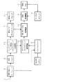
図1はこの発明の実施の形態1である受信装置を示すもので、図において、1はMPEG2トランスポートストリームをペイロードとするIEEE1394入力パケット信号である。2はIEEE1394パケット構造からペイロードを抽出するIEEE1394インターフェース、3はペイロードである分割されたMPEG2トランスポートストリームを再構成するためのFIFOメモリ、12はソースパケットヘッダ除去/ タイムスタンプ抽出装置で、SPH を抽出除去し、後段のMPEG2 TS デマルチプレクサにMPEG2
トランスポートストリームを転送する。
【0016】
7はMPEG2 TS デマルチプレクサで、PCR を抽出してMPEG2 A/V デコーダ11へMPEG2ストリームを転送する。5はサイクルタイマで、IEEE1394インターフェース2で検出したサイクルスタートパケットから絶対時間情報により125μs 毎に更正されるIEEE1394の絶対時刻を計時する。13はサイクルタイマ、タイムスタンプ保持装置で、ソースパケットヘッダ除去/タイムスタンプ抽出装置12で抽出したSPH を保持し、さらにソースパケットヘッダ除去/タイムスタンプ抽出装置12からMPEG2 TS デマルチプレクサ7にMPEG2トランスポートストリームを転送したときのサイクルタイマ値を保持する。
【0017】
8はクロック再生された27MHz のシステムクロックでカウントされるクロック再生のためのローカルカウンタ、10は27MHz のVCXO、9はVCXO10を制御するVCXO制御装置、14はPCR 補正/差分計算装置で、サイクルタイマ、タイムスタンプ保持装置13からの各情報とMPEG2 TS デマルチプレクサ7から抽出したPCRよりPCR を補正し、ローカルカウンタ8のカウンタ値との差分を求めてVCXO制御装置9に転送し、27MHzシステムクロック再生のためのフェーズドロックループ(PLL)を構成する。
【0018】
ソースパケットヘッダ除去/タイムスタンプ抽出装置12では、従来技術のようにMPEG2トランスポートストリームをSPHが表す時刻までバッファリングせずに即、MPEG2 TS デマルチプレクサ7に転送する。このためMPEG2 TS デマルチプレクサ7に入力されるMPEG2トランスポートストリームには、1394バスを伝送してきたことによるジッタが除去されず含まれている。このためMPEG2 TS デマルチプレクサ7で抽出されるPCR にもジッタが含まれており、これをそのままリファレンスとしてクロックリカバリに使用すると、誤ったクロックリカバリをしてしまうことになる。
【0019】
そこで、このジッタを補償する手段が必要となる。MPEG2 TS デマルチプレクサ7には、その前段でジッタ吸収のための時間管理およびバッファリング処理がされずにMPEG2トランスポートストリームが入力される。このため抽出したPCR値は、本来届くべき時刻よりも早めに抽出されることになる。
【0020】
従来技術では図4のVCXO制御装置9においてローカルカウンタ値と抽出したPCRの値を比較し、その差分値に応じて27MHzVCXO10が発生する周波数をコントロールする。もし早めに抽出されたPCR をそのまま従来技術と同じ処理をVCXO制御装置9で行うと、PCR 値は、本来検出されるべきタイミングより早めに抽出されているので、ローカルカウンタ値と比べて大きな値になっているはずであるので、ローカルカウンタをインクリメントする27MHz クロック周波数が遅いと判断し、27MHzVCXO10の出力周波数を上げる制御をしてしまうことになる。
【0021】
しかし、実際は27MHzのシステムクロック周波数が低かったわけでなく、バッファリングされずに本来到着するタイミングより早めにMPEG2トランスポートストリームがMPEG2 TS デマルチプレクサ7に入力されたのが原因である。この問題を補償するために、どれだけ早く抽出されてしまったかを図1のPCR補正/差分計算装置14で計算し、その分の値だけPCR 値に加算してPCR値を補正することで対応できる。
【0022】
この処理をPCR補正/差分計算装置14が以下のようににPCR補正を行う。
図2において、δは1394バス上の最大遅延時間、ti は、188バイトのMPEGトランスポートパケットに4バイトのタイムスタンプ(Tstmpi=ti+δ) を付加し、192バイトのソースパケットをIEEE1394バス上に送信する時刻、tcyciは受信側で1トランスポートパケットが再構成されMPEGデマルチプレクサに転送した時刻、tjiは1394バスによる伝送ジッタとする。
【0023】
PCR補正/差分計算装置14で下式に従ってジッタ量に応じたPCR 補正を行う。補正したPCRi値をPCRcoriとし、PCRi値およびPCR補正/差分計算装置14で補正したPCRcori値を時刻換算した値をそれぞれtPCRi、tPCR_coriとし、以下の補正を行う。
tPCR_cori=tPCRi+tji ………………………(1)
ここでtjiは図2より
tjt=tcyci−ti ………………………(2)
となる。Tstmpiは送信時刻tiに最大遅延時間δを加えた値なので、
Tstmpi=ti+δ ………………………(3)
となる。よって(2)式、(3)式より
tjt=tcyci−(Tstmpi−δ) ………………………(4)
となる。
【0024】
PCR 補正/差分計算装置14では、時間的に隣り合うPCR 値およびローカルカウンタ値のそれぞれの変化量ΔPCR、ΔLMの値を求め、VCXO制御装置9では、その誤差量に応じた制御電値を発生する。この計算では、PCRの代わりに補正したPCR 値を用いる。そこでΔPCRcoriの時刻換算値、tPCR_coriを(1),(4)を用いて求めると、

【0025】
よって、PCR 補正/差分計算装置14では、(5)式のようにMPEG2 TS デマルチプレクサ7からのPCR値からΔPCRの時刻換算値ΔtPCRを、サイクルタイマ、タイムスタンプ保持装置13からΔtcyc、ΔTstmpを計算し(5)式に代入してΔtPCR_coriを求める。
【0026】
さらにPCR補正/差分計算装置14でローカルカウンタ値と補正したPCR値との差分を求め、VCXO制御装置9で(6)式に従いVCXOコントロール電圧Vctrlを発生する。
Vctrl=G(ΔtPCR_cor−ΔtLMC i ) ………… (6)
ここでGはゲイン、ΔtLMCはローカルカウンタ値の時刻換算値である。
(6)式に従って発生されるコントロール電圧によって27MHzVCXO10は正確にシステムクロックを再生することができる。
【0027】
このような構成となっているからMPEG2 TS デマルチプレクサ7へMPEG2トランスポートストリームを転送するタイミングを監視する必要がなく、従来技術では必要だったSPHの値とサイクルタイマの値を逐次比較する手段が必要ない。このためソフトウエアで構成した場合には、SPHとサイクルタイマ値を常時比較する処理が不要となり、また高速なCPUが不要となる。一方ハードウエアで構成した場合であっても、余分な比較演算回路が不要となり、また余分なバッファも不要となる。
【0028】
実施の形態2.
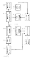
図3では図1のPCR補正/差分計算装置14の代わりにLMC 補正/差分計算装置15を使用した受信装置である。
図3のソースパケットヘッダ除去/タイムスタンプ抽出装置12では、従来技術のようにMPEG2トランスポートストリームをSPH が表す時刻までバッファリングせずに即、MPEG2 TS デマルチプレクサ7に転送する。
このためMPEG2 TS デマルチプレクサ7に入力されるMPEG2トランスポートストリームには、1394バスを伝送してきたことによるジッタが除去されず含まれている。このためMPEG2 TS デマルチプレクサ7で抽出されるPCRにもジッタが含まれており、これをそのままリファレンスとしてクロックリカバリに使用すると誤ったクロックリカバリをしてしまうことになる。
【0029】
そこでこのジッタを補償する手段が必要となる。MPEG2 TS デマルチプレクサ7にはその前段でジッタ吸収のための時間管理およびバッファリング処理がされずにMPEG2 トランスポートストリームが入力される。このため抽出したPCR値は、本来届くべき時刻よりも早めに抽出されることになる。従来技術では図4のVCXO制御装置9においてローカルカウンタ値と抽出したPCR の値を比較し、その差分値に応じて27MHzVCXO10が発生する周波数をコントロールする。
【0030】
もし早めに抽出されたPCR をそのまま従来技術と同じ処理をVCXO制御装置9で行うと、PCR値は、本来検出されるべきタイミングより早めに抽出されているので、ローカルカウンタ値と比べて大きな値になっているはずであるので、ローカルカウンタをインクリメントする27MHzクロック周波数が遅いと判断し、27MHzVCXO10の出力周波数を上げる制御をしてしまうことになる。
【0031】
しかし、実際は27MHzのシステムクロック周波数が低かったわけでなく、バッファリングされずに本来到着するタイミングより早めにMPEG2トランスポートストリームがMPEG2 TS デマルチプレクサ7に入力されたのが原因である。この問題を補償するために、どれだけ早く抽出されてしまったかを図3のLMC補正/差分計算装置15で計算し、その分の値だけローカルカウンタ値を減算してローカルカウンタ値を補正することで対応できる。
【0032】
この処理をLMC補正/差分計算装置15が以下のようにローカルカウンタ補正を行う。補正した時刻計測カウンタ値の時刻換算した値をtLMCcori、タイムスタンプ値を時刻換算した値をtstmpiとし以下の補正を行う。
tLMCcori =tLMCi− tji …………………(7)
となる。(7)式に(4)式を代入すると
tLMCcori =tLMCi−tcyci−(Tstmp−δ) ……………(8)
となる。
【0033】
図3のLMC補正/差分計算装置15では時間的に隣り合うPCR値およびローカルカウンタ値のそれぞれの変化量ΔPCR 、ΔLMCの値の誤差を求め、VCXO制御装置9では、その誤差量に応じた制御電圧を発生する。この計算では、LMCの代わりに補正したLMC値を用いる。そこでΔtLMCcoriの時刻換算値、ΔtLMC_coriを(8)式を用いて求めると、
【0034】
よって、ローカルカウンタ値からΔLMCの時刻換算値ΔtLMCを、図3のサイクルタイマ/タイムスタンプ保持装置13からΔtcyc、ΔTstmpを計算し上式に代入してΔtLMC_coriを求める。
【0035】
さらにLMC補正/差分計算装置15でローカルカウンタ値と補正したPCR値との差分を求めVCXO制御装置9で(10)式に従いVCXOコントロール電圧Vctrlを発生する。
Vctrl=G(ΔtPCR−ΔtLMC_cori) ………… (10)
ここでGはゲイン、ΔtLMCはローカルカウンタ値の時刻換算値である。
(10)式に従って発生されるコントロール電圧によって27MHzVCXO10は正確にシステムクロックを再生することができる。
【0036】
このような構成となっているからMPEG2 TS デマルチプレクサ7へMPEG2トランスポートストリームを転送するタイミングを監視する必要がなく、従来技術では必要だったSPH の値とサイクルタイマの値を逐次比較する手段が必要ない。このためソフトウエアで構成した場合には、SPHとサイクルタイマ値を常時比較する処理が不要となり、また高速なCPUが不要となる。一方ハードウエアで構成した場合であっても、余分な比較演算回路が不要となり、また余分なバッファも不要となる。
【0037】
【発明の効果】
この発明は、以上説明したように、タイムスタンプとペイロード出力時刻とに基づいて時刻基準参照値を補正することにより、前記タイムスタンプで指定されるタイミングよりも先にペイロードが出力されてもシステムクロックの周波数を正確に制御することができる。
【図面の簡単な説明】
【図1】 この発明の実施の形態1を示すブロック構成図である。
【図2】 実施の形態1のMPEG2 トランスポートパケットの送信受信方法の説明図である。
【図3】 この発明の実施の形態2を示すブロック構成図である。
【図4】 従来の信号受信装置の構成を示すブロック図である。
【図5】 パケット信号受信装置に入力するMPEG2トランスポートストリームをペイロードとするIEEE1394パケットの構成図である。
【図6】 MPEG2トランスポートパケットのフォーマット図である。
【符号の説明】
1 IEEE1394バス、2 IEEE1394インターフェース、3 FIFOメモリ、4 タイムスタンプ抽出装置、5 サイクルタイマ、6 出力タイミング制御装置、7 MPEG2 TS デマルチプレクサ、8 ローカルカウンタ、9 VCXO制御装置、
10 27MHzVCXO 、11 MPEG2 A/V デコーダ、12 ソースパケットヘッダ除去/タイムスタンプ抽出装置、13 サイクルタイマ、タイムスタンプ保持装置、14 PCR補正/差分計算装置、15 LMC補正/差分計算装置。[0001]
BACKGROUND OF THE INVENTION
The present invention relates to an apparatus provided in a packet signal receiving apparatus for regenerating a clock necessary for restoring a received packet.
[0002]
[Prior art]
FIG. 4 shows an example of a conventional signal receiving apparatus composed of devices conforming to IEEE1394, ISO / IEC 13818-1, -2 and 3, HD DIGITAL VCR CONFERENCE PART4 Specifications of MPEG DATA Transmission for Consumer-Use Digital Interface. In the block diagram showing the configuration, it is an apparatus for receiving an MPEG2 transport stream on a high-speed serial bus IEEE1394 bus.
[0003]
In the figure, 1 is an IEEE1394 bus that has a high-speed transfer band but includes jitter, 2 is an IEEE1394 interface that receives packets transmitted on the IEEE1394
[0004]
6 is an output timing control device for notifying the time
[0005]
When receiving the transfer notification from the output
[0006]
In the above system, the output
[0007]
[Problems to be solved by the invention]
In the conventional processing as described above, the output timing control device notifies the timing for transferring the MPEG2 transport stream to the MPEG2 TS demultiplexer. In order to detect the timing, it is necessary to always compare the value of the cycle timer with the value of the time stamp extracted by the time stamp extraction device. When this processing is realized by software, since comparison operations must be continuously performed, the load required for this processing increases, which greatly affects the performance of other software processing.
[0008]
In addition, when the result of the comparison operation matches, unless data is instantaneously transferred to the MPEG2 TS demultiplexer, the 27 MHz clock recovery is affected, so a high-speed CPU is required. On the other hand, if the output timing control device is realized by hardware, an extra 32-bit comparison operation circuit is required. Further, since the data must be held in the time stamp extraction device until the cycle timer value becomes equal to the time stamp value, an extra buffer is required.
[0009]
The present invention has been made for the purpose of solving the above-described problems, and an object of the present invention is to provide a clock recovery device that can execute accurate clock recovery with a simple configuration regardless of whether the configuration is software or hardware. To do.
[0010]
[Means for Solving the Problems]
Clock reproducing apparatus according to the invention, included in the packet that is input via the transfer sending passage, the time stamp, the payload, and extracts the clock reference, earlier than the timing specified by the time stamp Packet data output means for outputting the payload, payload output time detection means for detecting a payload output time corresponding to the time when the payload was output from the packet data output means, the time stamp and the payload output time, A time base reference value correcting means for correcting the time base reference value based on the output and a system clock for controlling the frequency of the system clock used for reproducing the payload based on the output of the time base reference value correcting means And a frequency control means .
[0011]
A packet data output means for extracting a time stamp and a payload included in a packet input via a transmission path, and outputting the payload before a timing specified by the time stamp; Payload output time detecting means for detecting a payload output time corresponding to the time when the payload was output from the packet data output means, and based on the time stamp and the payload output time, a system clock used for reproducing the payload A count value correction unit that corrects and outputs a count value obtained by counting the number, and a system clock frequency control unit that controls the frequency of the system clock based on the output of the count value correction unit. is there.
[0013]
DETAILED DESCRIPTION OF THE INVENTION
Hereinafter, the present invention will be specifically described with reference to the drawings showing embodiments thereof.
The communication system includes a transmission device and a reception device, and transmits the MPEG2 transport stream from the transmission device via the IEEE1394
[0014]
Further, in order to effectively use the bandwidth of the IEEE1394 bus, the source packet is divided into a plurality of pieces according to the transfer rate, and a header is added to form an IEEE1394 packet. Furthermore, a packet carrying absolute time information on the bus called a cycle start packet is transmitted every 125 μs on the IEEE1394 bus. The MPEG2 transport stream is composed of one packet of 188 bytes as shown in FIG. 6, and a program clock reference (PCR) is provided so that the receiving side can correctly reproduce the system clock on the transmitting side and can correctly reproduce the MPEG2 stream. Is included.
[0015]
FIG. 1 shows a receiving apparatus according to the first embodiment of the present invention. In FIG. 1,
Transfer the transport stream.
[0016]
Reference numeral 7 denotes an MPEG2 TS demultiplexer which extracts PCR and transfers the MPEG2 stream to the MPEG2 A /
[0017]
[0018]
The source packet header removal / time
[0019]
Therefore, a means for compensating for this jitter is required. An MPEG2 transport stream is input to the MPEG2 TS demultiplexer 7 without performing time management and buffering processing for jitter absorption in the preceding stage. For this reason, the extracted PCR value is extracted earlier than the time it should originally arrive.
[0020]
In the prior art, the VCXO controller 9 in FIG. 4 compares the local counter value with the extracted PCR value, and controls the frequency generated by the 27
[0021]
However, the system clock frequency of 27 MHz is not actually low, and this is because the MPEG2 transport stream is input to the MPEG2 TS demultiplexer 7 earlier than the original arrival timing without being buffered. In order to compensate for this problem, the PCR correction / difference calculation unit 14 in FIG. 1 calculates how early the extraction has been performed, and the corresponding value is added to the PCR value to correct the PCR value. it can.
[0022]
The PCR correction / difference calculation unit 14 performs PCR correction for this processing as follows.
In FIG. 2, δ is the maximum delay time on the 1394 bus, t i is a 188-byte MPEG transport packet with a 4-byte time stamp (T stmpi = t i + δ), and a 192-byte source packet. The transmission time on the IEEE 1394 bus, t cyci is the time when one transport packet is reconstructed on the receiving side and transferred to the MPEG demultiplexer, and t ji is the transmission jitter by the 1394 bus.
[0023]
The PCR correction / difference calculation unit 14 performs PCR correction according to the jitter amount according to the following equation. The corrected PCR i values and PCR cori, PCR i values and PCR correction / difference calculation unit 14 by the corrected PCR cori values the time-converted value respectively t PCRi, and t PCR _ cori, performs the following correction.
t PCR _ cori = t PCRi + t ji ........................... (1)
Here, t ji is t jt = t cyci −t i from FIG. 2 (2)
It becomes. Since T stmpi is a value obtained by adding the maximum delay time δ to the transmission time t i ,
T stmpi = t i + δ (3)
It becomes. Therefore, from formulas (2) and (3), t jt = t cyci- (T stmpi -δ) (4)
It becomes.
[0024]
The PCR correction / difference calculation unit 14 obtains the values ΔPCR and ΔLM of the respective temporally adjacent PCR values and local counter values, and the VCXO control unit 9 generates a control power value corresponding to the error amount. To do. In this calculation, corrected PCR values are used instead of PCR. Therefore, when the time conversion value of ΔPCR cori , t PCR _ cori is obtained using (1) and (4),
[0025]
Therefore, in the PCR correction / difference calculation device 14, ΔPCR is converted from the PCR value from the MPEG2 TS demultiplexer 7 to the time-converted value ΔtPCR of ΔPCR, and Δt cyc , ΔT stmp from the cycle timer and time stamp holding device 13. Is calculated and substituted into equation (5) to obtain Δt PCR — cori .
[0026]
Further obtains a difference between the PCR value corrected with the local counter value at PCR correction / difference calculation unit 14 generates a VCXO control voltage V ctrl according (6) in VCXO controller 9.
V ctrl = G (Δt PCR — cor −Δt LMC i ) (6)
Here, G is a gain, and Δt LMC is a time converted value of a local counter value.
The 27
[0027]
With this configuration, there is no need to monitor the timing of transferring the MPEG2 transport stream to the MPEG2 TS demultiplexer 7, and there is a means for sequentially comparing the SPH value and the cycle timer value, which was necessary in the prior art. unnecessary. For this reason, when it is configured by software, processing for constantly comparing SPH and cycle timer value is not required, and a high-speed CPU is not required. On the other hand, even in the case of hardware configuration, an extra comparison operation circuit is unnecessary and an extra buffer is also unnecessary.
[0028]
FIG. 3 shows a receiving apparatus using an LMC correction / difference calculation apparatus 15 instead of the PCR correction / difference calculation apparatus 14 of FIG.
The source packet header removal / time
For this reason, the MPEG2 transport stream input to the MPEG2 TS demultiplexer 7 includes jitter without being removed due to transmission through the 1394 bus. For this reason, jitter is also included in the PCR extracted by the MPEG2 TS demultiplexer 7. If this is used as a reference for clock recovery as it is, erroneous clock recovery will occur.
[0029]
Therefore, a means for compensating for this jitter is required. An MPEG2 transport stream is input to the MPEG2 TS demultiplexer 7 without performing time management and buffering processing for absorbing jitter in the preceding stage. For this reason, the extracted PCR value is extracted earlier than the time it should originally arrive. In the prior art, the VCXO controller 9 in FIG. 4 compares the local counter value with the extracted PCR value, and controls the frequency generated by the 27
[0030]
If the PCR extracted earlier is directly processed by the VCXO control device 9 as it is in the prior art, the PCR value is extracted earlier than the timing to be originally detected, and therefore a larger value than the local counter value. Therefore, it is determined that the 27 MHz clock frequency for incrementing the local counter is slow, and control is performed to increase the output frequency of the 27
[0031]
However, the system clock frequency of 27 MHz is not actually low, and this is because the MPEG2 transport stream is input to the MPEG2 TS demultiplexer 7 earlier than the original arrival timing without being buffered. In order to compensate for this problem, the LMC correction / difference calculation device 15 in FIG. 3 calculates how early the extraction has been performed, and corrects the local counter value by subtracting the local counter value by that amount. It can respond.
[0032]
In this process, the LMC correction / difference calculation apparatus 15 performs local counter correction as follows. The following correction is performed with the time-converted value of the corrected time measurement counter value being t LMCcori and the time-converted time-converted value being t stmpi .
t LMCcori = t LMCi -t ji ………………… (7)
It becomes. Substituting equation (4) into equation (7), t LMCcori = t LMCi −t cyci − (T stmp −δ) (8)
It becomes.
[0033]
The LMC correction / difference calculation device 15 of FIG. 3 obtains errors in the values ΔPCR and ΔLMC of the PCR values and local counter values that are temporally adjacent to each other, and the VCXO control device 9 performs control according to the error amount. Generate voltage. In this calculation, a corrected LMC value is used instead of the LMC. Therefore the time-converted value of Delta] t LMCcori, when determined using the Δt LMC _ cori (8) formula,
[0034]
Therefore, the time conversion value Delta] t LMC of ΔLMC from local counter value to determine the Delta] t LMC _ cori are substituted into the above equation to calculate the Delta] t cyc, [Delta] T stmp from the cycle timer / time stamp holding unit 13 of FIG. 3.
[0035]
Further, the difference between the local counter value and the corrected PCR value is obtained by the LMC correction / difference calculation device 15, and the VCXO control device 9 generates the VCXO control voltage V ctrl according to the equation (10).
V ctrl = G (Δt PCR -Δt LMC _ cori) ............ (10)
Here, G is a gain, and Δt LMC is a time converted value of a local counter value.
The 27
[0036]
With this configuration, there is no need to monitor the timing for transferring the MPEG2 transport stream to the MPEG2 TS demultiplexer 7, and a means for sequentially comparing the SPH value and the cycle timer value required in the prior art. unnecessary. For this reason, when it is configured by software, processing for constantly comparing SPH and cycle timer value is not required, and a high-speed CPU is not required. On the other hand, even in the case of hardware configuration, an extra comparison operation circuit is unnecessary and an extra buffer is also unnecessary.
[0037]
【The invention's effect】
As described above, the present invention corrects the time base reference value based on the time stamp and the payload output time, so that the system clock can be output even if the payload is output earlier than the timing specified by the time stamp. Can be accurately controlled.
[Brief description of the drawings]
FIG. 1 is a block configuration diagram showing a first embodiment of the present invention.
FIG. 2 is an explanatory diagram of an MPEG2 transport packet transmission / reception method according to the first embodiment;
FIG. 3 is a block configuration diagram showing a second embodiment of the present invention.
FIG. 4 is a block diagram showing a configuration of a conventional signal receiving apparatus.
FIG. 5 is a configuration diagram of an IEEE1394 packet having an MPEG2 transport stream input to the packet signal receiving apparatus as a payload.
FIG. 6 is a format diagram of an MPEG2 transport packet.
[Explanation of symbols]
1 IEEE1394 bus, 2 IEEE1394 interface, 3 FIFO memory, 4 time stamp extractor, 5 cycle timer, 6 output timing controller, 7 MPEG2 TS demultiplexer, 8 local counter, 9 VCXO controller,
10 27 MHz VCXO, 11 MPEG2 A / V decoder, 12 source packet header removal / time stamp extraction device, 13 cycle timer, time stamp holding device, 14 PCR correction / difference calculation device, 15 LMC correction / difference calculation device.
Claims (5)
このパケットデータ出力手段から前記ペイロードが出力された時刻に対応するペイロード出力時刻を検出するペイロード出力時刻検出手段と、
前記タイムスタンプと前記ペイロード出力時刻とに基づいて前記時刻基準参照値を補正して出力する時刻基準参照値補正手段と、
この時刻基準参照値補正手段の出力に基づいて、前記ペイロードの再生に用いるシステムクロックの周波数を制御するシステムクロック周波数制御手段とを備えるクロック再生装置。 Included in a packet inputted via the transfer sending passage, the time stamp, the payload, and extracts the clock reference, a packet data output for outputting the payload before the timing specified by the time stamp Means,
Payload output time detection means for detecting a payload output time corresponding to the time when the payload was output from the packet data output means;
Time reference reference value correcting means for correcting and outputting the time reference reference value based on the time stamp and the payload output time;
A clock recovery apparatus comprising system clock frequency control means for controlling the frequency of a system clock used for reproducing the payload based on the output of the time reference reference value correction means .
このパケットデータ出力手段から前記ペイロードが出力された時刻に対応するペイロード出力時刻を検出するペイロード出力時刻検出手段と、
前記タイムスタンプと前記ペイロード出力時刻とに基づいて、前記ペイロードの再生に用いるシステムクロックの個数をカウントして得られるカウント値を補正して出力するカウント値補正手段と、
このカウント値補正手段の出力に基づいて、前記システムクロックの周波数を制御するシステムクロック周波数制御手段とを備えるクロック再生装置。 A packet data output means for extracting a time stamp and a payload included in a packet input via a transmission path, and outputting the payload before a timing specified by the time stamp;
Payload output time detection means for detecting a payload output time corresponding to the time when the payload was output from the packet data output means;
Count value correcting means for correcting and outputting a count value obtained by counting the number of system clocks used for reproducing the payload based on the time stamp and the payload output time;
A clock recovery apparatus comprising system clock frequency control means for controlling the frequency of the system clock based on the output of the count value correction means .
Priority Applications (1)
| Application Number | Priority Date | Filing Date | Title |
|---|---|---|---|
| JP11536898A JP3642180B2 (en) | 1998-04-24 | 1998-04-24 | Clock regenerator |
Applications Claiming Priority (1)
| Application Number | Priority Date | Filing Date | Title |
|---|---|---|---|
| JP11536898A JP3642180B2 (en) | 1998-04-24 | 1998-04-24 | Clock regenerator |
Publications (2)
| Publication Number | Publication Date |
|---|---|
| JPH11308203A JPH11308203A (en) | 1999-11-05 |
| JP3642180B2 true JP3642180B2 (en) | 2005-04-27 |
Family
ID=14660803
Family Applications (1)
| Application Number | Title | Priority Date | Filing Date |
|---|---|---|---|
| JP11536898A Expired - Fee Related JP3642180B2 (en) | 1998-04-24 | 1998-04-24 | Clock regenerator |
Country Status (1)
| Country | Link |
|---|---|
| JP (1) | JP3642180B2 (en) |
Families Citing this family (10)
| Publication number | Priority date | Publication date | Assignee | Title |
|---|---|---|---|---|
| KR20010006688A (en) * | 1999-02-26 | 2001-01-26 | 윤종용 | Method and apparatus for recovering data stream clock |
| WO2002009351A2 (en) * | 2000-07-26 | 2002-01-31 | Thomson Licensing S.A. | Multi-media jitter removal in an asynchronous digital home network |
| JP2002100113A (en) | 2000-09-25 | 2002-04-05 | Canon Inc | Reproducing device, reproducing method, transmission method and storage medium |
| JP4680444B2 (en) * | 2001-08-23 | 2011-05-11 | パナソニック株式会社 | Storage type data broadcasting system |
| CN1314269C (en) * | 2002-04-02 | 2007-05-02 | 中兴通讯股份有限公司 | Method and device for regulating program reference clock of motion image expert group 2 |
| JP4561822B2 (en) * | 2002-07-16 | 2010-10-13 | パナソニック株式会社 | Content receiver |
| AU2003281136A1 (en) | 2002-07-16 | 2004-02-02 | Matsushita Electric Industrial Co., Ltd. | Content receiving apparatus and content transmitting apparatus |
| JP4905060B2 (en) * | 2006-11-07 | 2012-03-28 | 富士通株式会社 | Reception device and data reproduction method |
| JP4679502B2 (en) * | 2006-12-18 | 2011-04-27 | Kddi株式会社 | Voice packet reproducing apparatus, communication terminal and program having clock correction function |
| JP2009239449A (en) * | 2008-03-26 | 2009-10-15 | Nec Electronics Corp | Precise synchronization type network device, network system, and frame transfer method |
-
1998
- 1998-04-24 JP JP11536898A patent/JP3642180B2/en not_active Expired - Fee Related
Also Published As
| Publication number | Publication date |
|---|---|
| JPH11308203A (en) | 1999-11-05 |
Similar Documents
| Publication | Publication Date | Title |
|---|---|---|
| JP4896293B2 (en) | Method and apparatus for isochronous data communication | |
| US7756233B2 (en) | Data receiving device and data receiving method | |
| US7778277B2 (en) | Timing recovery method and system thereof | |
| JP5223427B2 (en) | Clock synchronization system | |
| JP2002064788A (en) | Data stream processor and method, and program storage medium | |
| JPH0897807A (en) | Packet transmission system | |
| JP2001036549A (en) | Data processing system and time stamp generating method | |
| JP2000099485A (en) | Distributed system reinforcing time synchronization | |
| JP3642180B2 (en) | Clock regenerator | |
| US6757304B1 (en) | Method and apparatus for data communication and storage wherein a IEEE1394/firewire clock is synchronized to an ATM network clock | |
| JP3810918B2 (en) | Multimedia data relay apparatus and method | |
| US6895009B1 (en) | Method of generating timestamps for isochronous data | |
| JPH09224008A (en) | Audio reproduction time adjustment circuit | |
| JP3499818B2 (en) | Time stamp offset adjusting method and packet transmission device using the same | |
| EP2337392B1 (en) | Time sequence number jumping detecting and processing method and device | |
| JP2000332831A (en) | Communication device, communication method and recording medium | |
| US7869467B2 (en) | Receiving device including packet output circuit for outputting control signal | |
| US20030053795A1 (en) | Data stream processing device and method and program storage medium | |
| JP3827297B2 (en) | Transmission device, reception device, network, transmission method, and reception method | |
| JP3546799B2 (en) | Data transceiver | |
| JP4015381B2 (en) | LAN controller and transmission apparatus equipped with LAN controller | |
| JP3801043B2 (en) | Data receiving apparatus and method | |
| CN114339348B (en) | PCR correction method and system based on frequency offset detection and compensation | |
| JP3632577B2 (en) | Data transmission device | |
| JP4382230B2 (en) | Transmission apparatus and method in video storage and playback system using MPEG2 encoding technology |
Legal Events
| Date | Code | Title | Description |
|---|---|---|---|
| RD01 | Notification of change of attorney |
Free format text: JAPANESE INTERMEDIATE CODE: A7421 Effective date: 20040628 |
|
| A977 | Report on retrieval |
Free format text: JAPANESE INTERMEDIATE CODE: A971007 Effective date: 20041224 |
|
| TRDD | Decision of grant or rejection written | ||
| A01 | Written decision to grant a patent or to grant a registration (utility model) |
Free format text: JAPANESE INTERMEDIATE CODE: A01 Effective date: 20050105 |
|
| A61 | First payment of annual fees (during grant procedure) |
Free format text: JAPANESE INTERMEDIATE CODE: A61 Effective date: 20050118 |
|
| FPAY | Renewal fee payment (event date is renewal date of database) |
Free format text: PAYMENT UNTIL: 20080204 Year of fee payment: 3 |
|
| FPAY | Renewal fee payment (event date is renewal date of database) |
Free format text: PAYMENT UNTIL: 20090204 Year of fee payment: 4 |
|
| FPAY | Renewal fee payment (event date is renewal date of database) |
Free format text: PAYMENT UNTIL: 20100204 Year of fee payment: 5 |
|
| FPAY | Renewal fee payment (event date is renewal date of database) |
Free format text: PAYMENT UNTIL: 20100204 Year of fee payment: 5 |
|
| FPAY | Renewal fee payment (event date is renewal date of database) |
Free format text: PAYMENT UNTIL: 20110204 Year of fee payment: 6 |
|
| LAPS | Cancellation because of no payment of annual fees |