JP3634465B2 - Connectionless communication system, its test method, and in-station control system - Google Patents
Connectionless communication system, its test method, and in-station control system Download PDFInfo
- Publication number
- JP3634465B2 JP3634465B2 JP26134695A JP26134695A JP3634465B2 JP 3634465 B2 JP3634465 B2 JP 3634465B2 JP 26134695 A JP26134695 A JP 26134695A JP 26134695 A JP26134695 A JP 26134695A JP 3634465 B2 JP3634465 B2 JP 3634465B2
- Authority
- JP
- Japan
- Prior art keywords
- path
- route
- cell
- station
- exchange
- Prior art date
- Legal status (The legal status is an assumption and is not a legal conclusion. Google has not performed a legal analysis and makes no representation as to the accuracy of the status listed.)
- Expired - Fee Related
Links
Images


Landscapes
- Monitoring And Testing Of Exchanges (AREA)
- Data Exchanges In Wide-Area Networks (AREA)
- Telephonic Communication Services (AREA)
Description
【0001】
【発明の属する技術分野】
本発明は、高速データ伝送を行うコネクションレス通信システムとその試験方法に関し、また、高速データ伝送のための交換局の局内制御方式に関する。
【0002】
【従来の技術】
近年、ワークステーションやパーソナルコンピュータ等の情報処理装置の高性能化に伴い、多数の情報処理装置を高速LAN (ローカル・エリア・ネットワーク)で接続した分散処理が広く行われている。そして、これらLAN 間を接続するネットワークに対しても高速化が要求されている。
上述のような高速データ通信を実現するサービスの一つとしてSMDSが知られている。SMDS(Switched Multi−megabit Data Service )は、1.5Mbps 及び45Mbpsの転送速度を基本としたコネクションレス型のデータ交換サービスである。
ところで、広帯域ISDNを実現する方法としては、ATM 方式が知られているが、ATM ネットワークの中でSMDSを提供することができる。この場合、所定のATM 交換機に対してSMDS処理用サーバ(SMDSメッセージハンドラ)を設ける。そして、SMDS加入者とそのSMDS加入者を収容するSMDS処理用サーバとの間を、PVC (Permanent Virtual Circuit またはPermanent Virtual Channel )で接続し、SMDS加入者から出力されるコネクションレスデータをSMDS処理用サーバへ転送して、そのサーバにおいてルーティング処理等を実行させる。
ここで、上記コネクションレスデータは、一般に、可変長のパケット(データフレーム)であるが、上記PVC はATM ネットワーク上に設定されるパスであるので、コネクションレスデータは、ATM 交換機に入力される前にATM セル形式に変換(分解)して転送される。このセルは、48バイトのペイロード部と、5バイトのヘッダ部とからなる53バイト構成を基本としている。
そして、このATM セル形式のデータは、図897に示すように、SMDS処理用サーバでいったんL3−PDU(レイヤ3プロトコル・データ・ユニット)あるいはさらに上位レイヤのデータ形式に組立られ、L3−PDUに格納されている着信先アドレスDA、送信元アドレスSA等に基づいてルーティング情報などの解析が行われる。その後、再びセルに分解されて、上記解析した情報に基づいてルーティングされる。
上述したように、従来のSMDSにおいては、SMDS処理用サーバでルーティング処理等を行うときに、入力セルを上位レイヤのデータ形式(たとえば、L3−PDU)に組み立てて、マイコン・プログラム等のソフトウェアによってその処理を行っていたため、高速化には限界があった。また、着信先アドレスDAとしてグループアドレスが指定されていた場合のデータコピー処理、トラフィックの平滑化処理、EOM セル(End of Message:L3−PDUを複数のセルに分解した場合、そのL3−PDUの最後の部分のデータを格納するセル)の不着信時の処理等も、全てマイコン等によりソフト的に処理されていた。
このように、従来のSMDSでは、SMDS処理用サーバでの処理に様々なソフトウェア処理が含まれていたため、その高速化には限界があった。したがって、SMDSを用いてコネクションレス通信のデータ伝送を行う場合、伝送路・交換機の速度を高速化しても、SMDS処理用サーバでの処理がボトルネックとなって、実際の高速化が妨げられていた。さらに、SMDS処理用サーバにおいて上記組立処理を行う場合、各L3−PDUを構成するセルをいったんすべて格納する必要があるので、そのためのバッファ容量が大きくなってしまうという問題もあった。
次に、SMDSにおいては、サービス提供時に、以下に示すようなプロトコル・パフォーマンス・モニタリングを行う。すなわち、データに含まれる様々なパラメータについて、そのフォーマットチェック等を行う。そして、このチェックにおいて、NGとなったデータ(正常性を確認できなかったデータ)の個数をカウントする。また、予め決められた特定の種別のチェックに関しては、そのNG個数に対して所定のアルゴリズムに従った計数処理を行い、その結果が、予め設定した閾値を超過した場合はTCA (threshold crossing alart:閾値を越えたことを示すアラート) を出力する。さらに、特定の種別のチェックに関しては、NG検出時にエラーログを収集する。
エラーログにおいて収集すべきパラメータを以下に示す。
(1) 着信先アドレスDA(Destination Address )
(2) 送信元アドレスSA(Source Address)
(3) SNI 番号(Subscriber Network Interface No.)
(4) エラー種別
ところで、ユーザ(加入者)とSMDS処理用サーバとの間のPVC 上においては、前述したように、セルフォーマット(実際は、ATM セル形式で送受信が行われ、SMDS処理用サーバではL2−PDUで処理が行われる。ATM セル及びL2−PDUは、共に53バイトを基本構成としており、ここでは簡単のため、双方を単にセルと呼んでいる)でデータの転送を行う。ところが、上記のようなエラーログの収集はレイヤ3に関するものが多いため、SMDS処理用サーバにおいては、セル形式で受信したデータをいったんL3−PDUに組み立ててからその処理を行う。
上述のように、従来のSMDSにおいては、エラーログを収集する場合にも入力セルを上位レイヤのデータ形式(たとえば、L3−PDU)に組み立てて処理していた。このことが、SMDSにおける高速化処理の妨げとなっていた。
次に、上述のようなサービスは、ネットワークを構成する伝送路の物理的品質の信頼性が高いことを前提としている。このため、これらのネットワークの伝送品質を試験・評価することは重要である。
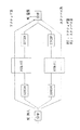
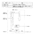
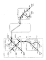
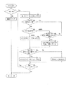
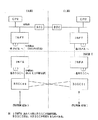
このような伝送路の試験・評価としては、コネクションレス通信サービスを提供しているネットワーク内において、OSセンター(ネットワークを管理するオペレーション・センター)から起動し、任意の局間リンク(交換機間のパス)の正常性を確かめる「局間ループバック試験」が行われている。この局間ループバック試験を、図898を参照しながら説明する。ここでは、SW局3とSW局6との間のリンクの試験を行うものとする。
試験の開始は、同図に示すように、まず、OSセンタ−1からSW局3に対して、試験用コネクションレスパケット送出要求メッセージ(試験開始要求)を送出する。この要求メッセージには、パケットの終着SW局6を示す識別情報IDが含まれている。SW局3は、その終着SW局6の識別アドレスを着信先アドレスDAとし、自局(SW局3)の識別アドレスを送信元アドレスSAとして試験用パケットを生成する。そして、その試験用パケットを終着SW局6に向けて出力する。
SW局4,SW局5においては、試験用パケットに対して通常のパケットと同様の処理を行い、終着SW局6へ転送する。終着SW局6では、試験用パケットを受信すると、そのパケットが有するDAとSAとを反転させて出力する。すなわち、上記終着SW局6から上記発SW局3へ向けてパケットが返送され、発SW局3に再び着信した時点でOSセンタ−1にその旨が報告される。
こうして、OSセンタ−1では、ネットワーク内でのパケットの伝達が正常に行われるかどうかの確認、すなわち伝送路(ここでは、SW局3とSW局6との間のリンク)の正常性を確認できる。また、この手順のなかで、発SW局3と終着SW局6はパケットのペイロード部分にタイムスタンプを刻印するため、この情報によりOSセンタ−1では、パケットの伝達時間を知ることができる。
しかし、上述の試験方式においては、その試験によって得られる情報はOSセンタ−(オペレーション・センター)のためのものであり、現在までのところ、加入者(図898における、端末2)がネットワークの伝送品質(伝達遅延時間等)を自主的に知る手段は提供されていなかった。このため、発信加入者からのパケットが着信先加入者に正常に届かないような場合、その加入者自身が加入者端末またはネットワーク側伝送路のどちらに障害要因があるのかを切り分けることがでず、障害からの復旧のためにはOSセンタ−を呼ぶ必要があり、そのために多大な時間とコストがかかっていた。
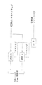
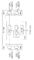
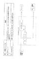
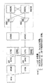
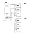
次に、図899に、SMDSの一実施形態を示す。同図において、SMDSサポートモジュールは、着信先アドレスDAの解析や各種チェックを行う。SMDSサポートモジュールS 部は、複数個の発SMDS加入者(a),(b) を収容し、DA解析や各種チェック等を行う。SMDSサポートモジュールR 部は、複数個の着SMDS加入者(x),(y) を収容し、各種チェック等を行う。これらS 部およびR 部から構成されるモジュールが、上述のSMDS処理用サーバ(SMDSメッセージハンドラ)に対応する。
各発SMDS加入者(a), (b)とSMDSサポートモジュールS 部との間はそれぞれPVC1,2によって接続され、SMDSサポートモジュールS 部とR 部との間はPVC 3によって接続され、そしてSMDSサポートモジュールR 部と各着SMDS加入者(x), (y)との間はそれぞれPVC 4,5で接続されている。
同図に示すSWをATM スイッチで構成した場合、発SMDS加入者(a),(b) から出力されるコネクションレスデータ(SMDSメッセージ)は、不図示のインタフェース部でセル形式に変換され、そのセルのヘッダ部に、着信先としてSMDSサポートモジュールを指定する特定のVPI/VCI 値(PVC 1,2を指定するVPI/VCI 値)を付与して転送することによって、SMDSサポートモジュールS 部に転送される。SMDSサポートモジュールS 部とR 部との間の転送では、PVC 3を示すVPI/VCI 値が付与されて出力され、さらに、SMDSサポートモジュールR 部から着SMDS加入者(x),(y) へ転送されるセルは、PVC 4,5を示す特定のVPI/VCI 値でSMDSサポートモジュールR 部から出力されて、着SMDS加入者(x),(y) に着信する。尚、各PVC はシステム初期設定時に確立される。
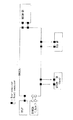
また、SMDSサポートモジュールS 部、R 部共に、収容可能な発・着SMDS加入者数には限度があるので、1つのSW局内にその最大収容数を超過するSMDS加入者を収容する場合は、複数個のSMDSサポートモジュールを用意する。この例を、図900に示す。この場合も、各接続は、PVC によって行う。同図は、SMDS加入者(a), (b), (x), (y)が、SMDSサポートモジュール▲1▼に収容され、SMDS加入者(c), (d), (v), (w)が、SMDSサポートモジュール▲2▼に収容される例を示しているである。なお、SMDSサポートモジュール▲1▼と▲2▼間にもPVC による接続が存在する。
上述のように、SMDSにおいては、データを転送するパスをPVC としてシステム初期設定時に確立してある。そして、発加入者(a),(b) がSMDSメッセージを出力すると、そのメッセージは上記PVC 1,2に沿ってSMDSサポートモジュールS 部に導かれ、PVC 3およびPVC 4,5を介して着SMDS加入者(x),(y) へ転送されるので、発SMDS加入者(a),(b) から出力されたSMDSメッセージが上記PVC に沿って確実に着SMDS加入者(x),(y) に届いているかのかを簡単に検証できない。
もし、上述のようなデータ転送が失敗した場合には、発加入者(a),(b) または着SMDS加入者(x),(y) からの苦情(コンプレイン)が発生することが予想されるが、この加入者コンプレインに対して、適切に(迅速に)上記検証がなされることが望まれる。また、このような検証を行う場合、出来るだけ低コストで実現することが望まれる。
ところで、PVC 試験および伝送時間などに関する試験については上述したが、SMDSにおいては、伝送されるSMDSデータの正常性の確認もする必要がある。データの正常性の確認方法としては、L3−PDUのBA−size, BE−tag, L2−PDU のLENGTHのチェック等が行われる。
BA−size チェックでは、L3−PDU(CPCS−PDU)のペイロード長を設定する値が正常かどうか確認する。BE−tag(Beginning Tag : 先頭タグ,End Tag : 最終タグ)チェックでは、L3−PDUの先頭と末尾の2つのタグが同一であることを検証することによってL3−PDUデータの正常性を確認する。LENGTHチェックは、L2−PDUの有効ペイロード長を示す値と、上記L3−PDUのBA−size との関係を検証することにより、L3−PDUとL2−PDUとの間での分解・組立が正常に行われたかを確認する。
しかし、この場合、L2−PDUに分解された状態でL3−PDUの正常性確認しようとすると、そのための回路の規模が極めて大きなものとなってしまう。また、L3−PDUのBA−size, BE−tag, L2−PDU LENGTHのチェックはそれぞれ互いに密接な関係があるため、各セル毎(L2−PDU毎)に処理を行うことは困難であった。一方、SMDS処理用サーバに入力されるセル形式のデータ(L2−PDU)を、いったんL3−PDUに組み立ててから処理すると、前述した問題と同様に、ソフトウェア処理が含まれることによって高速化が妨げられてしまう。
次に、ATM 交換ネットワークにおいてコネクションレス通信サービスを実現する場合には、コネクションレスデータ処理用サーバ(SMDSでは、SMDS処理用サーバ)を設け、加入者端末から出力されるコネクションレスデータのルーティング処理や各種チェック等を、そのサーバに依頼する。このようなコネクションレス通信サービスの実現方法の一例を図901に示す。
図901に示す構成は、基本的には図899に示した構成と同じである。すなわち、発信加入者(a) とコネクションレスデータ処理用サーバCLS 2との間にPVC 11が設定され、着信加入者(x) とコネクションレスデータ処理用サーバCLS 6との間にPVC 13が設定されている。これらのPVC は、コール・プロセッサCPR 3,7を用いて設定される。
図901に示す構成では、発信加入者(a) を収容するコネクションレスデータ処理用サーバCLS 2と着信加入者(x) を収容するコネクションレスデータ処理用サーバCLS 6とが異なる交換局に設けられた構成、即ち、コネクションレスデータ処理用サーバCLS 2は交換局SW1に対して設けられ、コネクションレスデータ処理用サーバCLS 6は交換局SW5に対して設けられた構成である。そして、これらコネクションレスデータ処理用サーバCLS 2,6間が、PVC 12によって接続されている。ここで、PVC 12が設定される大規模中継スイッチ4は、たとえば、SW1またはSW5と同じスイッチをいくつか中継させる構成、またはATM インターコネクション・スイッチ(AISW)である。
上記構成において、発信加入者(a) から着信加入者(x) にコネクションレスデータを転送する場合には、発信加入者(a) から出力されたデータは、PVC 11を介してコネクションレスデータ処理用サーバCLS 2に入力された後、PVC 12を介してコネクションレスデータ処理用サーバCLS 6へ転送される。そして、コネクションレスデータ処理用サーバCLS 6からPVC 13を介して着信加入者(x) へ転送される。これらPVC 上ではセル単位でのデータ転送が行われ、そのルーティング処理はコネクションレスデータ処理用サーバCLS 2および6によって行われる。
従来のコネクションレス通信サービスでは、図901に示したように、発信加入者(a) を収容するコネクションレスデータ処理用サーバCLS 2と着信加入者(x) を収容するコネクションレスデータ処理用サーバCLS 6とが異なる場合、それらコネクションレスデータ処理用サーバCLS 2,6間をPVC 12で接続している。そして、このPVC 12は、SW1,5および大規模中継スイッチ4と通過するように設定されている。このため、これらスイッチ内に予めコネクションレスサービス用の帯域リソースを確保し、その管理を行う必要がある。
したがって、従来のシステムでは、コネクションレスサービスのデータが流れていないときでも、各スイッチの帯域リソースを使用してしまっている。また、そのときの帯域リソースの管理も複雑なのもになっていた。
一方、ATM(Asynchronous Transfer Mode) サービス等の広帯域サービスを提供するB−ISDN (広帯域ISDN) 交換機、或いはSMDS(Switched Megabit Data Service) サービスを提供するSMDS交換機などの、セル交換を主体とした交換機は、従来の電話交換機又はN−IDSN (狭帯域ISDN) 交換機に比較して、格段に高い性能及び機能を有するため、その局内制御方式には独自の技術が必要とされる。
以下に、局内制御において本発明が対象とする従来技術及びその問題点について明らかにする。
まず、種々の伝送路インタフェース装置 (トランク) などの局内装置と交換機プロセッサとの間で制御情報の通信を行うための局内制御通信技術に関する課題について考察する。
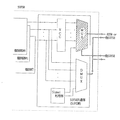
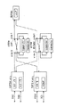
従来の交換システムにおける局内装置の制御においては、図902に示されるように、ATM スイッチ5と協調して動作する各局内装置6、7等が、入力制御装置4を介して、交換機プロセッサ(CC)1が接続されるシステムバス3に接続され、局内装置とCC1に接続される主記憶装置(MM)2との間で、DMA(ダイレクトメモリアクセス) 方式によって制御情報が転送されていた。
しかし、この方式では、全局内装置6、7をシステムバス3に接続しなくてはならず、各局内装置6、7とシステムバス3を接続するためのケーブルを装置数分用意する必要があり、局内装置6、7がシステムバス3から遠ければ遠いほどケーブルが長くなり接続構成上複雑になるという問題点を有している。
また、全局内装置6、7がシステムバス3に接続されることによりバスアクセスの際に必要となるアクセス権の獲得が競合し、バスアクセスが輻輳するという問題点も有している。
更に、システムバス3を各局内装置6、7まで延長することにより伝送品質が低下し、誤り制御手順を持たないDMA 手順では、データエラーやパリティエラーといった伝送エラーを発生するという問題点も有している。
次に、端末と交換機プロセッサなどの制御装置との間で呼設定情報等の制御情報の通信を行うための技術に関する課題につき考察する。
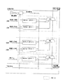
ATM交換システム等において、端末インタフェース装置を制御するには、交換機プロセッサ等の制御系装置との制御情報の通信が必要である。
制御情報の通信のための従来技術として、図903に示されるように、図902に示した場合と同様に、制御系装置(MPR1、PRIF2) から交換スイッチ(SW)3に接続される端末(TERM)4に、物理的なインタフェースが接続される方式がある。
しかし、この方式では、端末4毎に物理インタフェースが必要となるため、システム構成が複雑になり、また、端末4の増設が簡単ではないという問題点を有している。
次に、局内制御方式の1つである交換機の試験技術に関する課題につき考察する。
ATM 交換機等においては、セルが転送されるハイウエイに障害があるか否かの試験は、セルの送信や受信したセルの検索・収集を行うことのできる試験装置をハイウエイに接続することにより行われていた。この場合、宛先情報であるVPI (Virtual Path Identifier) 、VCI (Virtual Channel Identifier)、被試験装置内でセルを折り返す設定、その他LSI の設定などが試験装置から行われた後に、試験用のセルが送出されている。
しかし、このような方式では、複雑な構成の試験装置が必要となり、被試験装置への設定などに時間もかかるという問題点を有している。
次に、上述と同様の交換機の試験技術のうち、特にループバック試験に関する課題につき考察する。
音声・データ及び動画像などのようにトラヒック特性の異なる情報を結合して交換することのできるATM 交換機の普及とATM 交換網の拡大に従って、局間のパスの正常性を確認する試験の重要性も高くなっている。また、実際に運用に入っている状態で、いくつもの局を間に持つ2つの局の間に障害が発生した場合、より早期の障害の発見・修復が要求される。ATM 交換網のループバック試験方法はこの局間の障害の早期発見に有効な試験方法である。
ATM 交換機は市場に出始めたばかりである。ATM 交換網の局間試験について実例は未だない。しかし、従来の電子交換の試験方法の流れから次のような試験方法が、ATM 交換網の局間試験方法として考えられている。
この方法では試験装置がATM 交換機に接続され、オペレータによる操作によってループバック試験が行われる。試験時には相手局と連絡がとられ、相手局でも同様に試験装置がATM 交換機に接続され、連絡を取り合い、お互いの同期を取りながら試験が実施されることになる。
しかし、この方法では、ATM交換網の中に多数の局が存在した場合、それぞれの局に試験装置を配備する必要があるという問題点を有している。
また、試験装置の数が充分にない場合は、試験装置を持って各局を回り試験を行わなければならないという問題点も有している。
更に、局の中にはリモート局のように、オペレータが常時待機していない局もある。その場合、オペレータはその局まで行って試験を実施しなければならないという問題点を有している。
このように、上述の方法では、局間試験を行うためにオペレータに多大な労力が要求されるという問題点を有している。
次に、局内制御方式の1つである交換機スイッチ内のパフォーマンスの測定技術に関する課題につき考察する。
ATM を用いたSRM(Self Rooting Module)交換方式は、広帯域ISDNシステムを構築する際の前提条件であるが、このSRM 内のパフォーマンスを測定することは、従来困難であった。
次に、局内制御方式の1つである、ディジタル信号レベル3フォーマットであるDS3 フォーマットにインタフェースされる物理レイヤコンバージェンスプロトコルであるPLCPにおけるトレイラの制御に関する課題につき考察する。
B−ISDN又はSMDSのサービスにおいては、44.736MHz のサービスを実現するために、DS3(ディジタル信号レベル3) フォーマットが使用される。
本発明が対象とするシステム構成例を、図904及び図905に示す。図904は、BISDN端末がBISDN交換機に接続されている構成を示す。また、図905は、SMDS端末がSMDS交換機に接続されている構成を示す。本発明は、BISDN端末とBISDN交換機、又はSMDS端末とSMDS交換機の各送信部に関連する。
図906に、DS3 マルチフレーム構成を示す。DS3 のフレームは85ビット構成の基本フレームにより構成されている。基本フレームは1ビットのDS3 ヘッダと84ビットのDS3 ペイロードから構成されている。さらに8つの基本フレームで1つのサブフレームが構成されており、更に、7個のサブフレームで1つのマルチフレームが構成されている。即ち、1マルチフレームは、56個 (8×7) の基本フレームで構成されている。
BISDN のATM セルは53オクテット構成のセルであり、SMDSのL2−PDUセル (レベル2プロトコルデータユニットセル) も53バイト構成のセルである。即ち、基本構成は同じである。但し、ヘッダとペイロードの内容、HEC とHCS の値は異なっている。図907の(a) と(b) に、ATM セルとL2−PDUセルの構成を示す。
ATM セル又はL2−PDUセルは、直接DS3 基本フレームのペイロードに格納されるのではなく、PLCP (物理レイヤコンバージェンスプロトコル) のフレームを介して送信される。
図908に、DS3 フォーマットにインタフェースされるPLCPマルチフレームの構成を示す。
ATM セル又はL2−PDUセルは、PLCPフレーム内の53オクテットのPLCPペイロードにそれぞれ1セルずつ格納され、更に、PLCPマルチフレームは、それぞれ84ビットからなるセグメントに分割され、各セグメントがDS3 フレーム内の84オクテットのDS3 ペイロードに格納され、送信される。
PLCPフレームは4バイトのPLCPヘッダと53バイトのPLCPペイロードの繰り返し12個と、トレイラとからなる、マルチフレーム構成になっている。PLCPヘッダは、A1、A2バイトとPOHI、POH により構成される。トレイラ長は、13ニブル又は14ニブルである。ニブルとは4ビットのことであって、バイトの半分を示している。トレイラのデータは、4ビットのパターン”1100”が13個又は14個並べられたものである。
そして、PLCPの1マルチフレームは、平均して125 μsec(8KHz周期) で送信される。トレイラ長が可変であるため、平均値が規定される。
トレイラについて説明する。DS3 フレームは44.736MHz の伝送速度を有するため、以下の式から、125μsec の期間では、5592ビットが送信される。
【数1】
ビット数=44.736×10⁶ (ビット/sec) ×125 ×10−6(sec) =5592ビット
しかし、DS3 フレームを構成するデータは、図906に示したように、1ビットのフレームビットデータと、84ビットのDS3 ペイロードとから構成されているため、125 μsec の期間のDS3 ペイロードの部分のビット数は5592×84/85=5526.211・・・となって、割り切れない。
また、PLCPマルチフレーム中のビット数は、トレイラ長が13ニブルの時に、57×12×8+13×4 =5524ビットであり、トレイラ長が14ニブルの時に、57×12×8+14×4 =5528ビットである。即ち、トレイラ長が13ニブルの場合には125 μsec の期間のDS3 ペイロードにおいて余りが生じ、トレイラ長が14ニブルの場合には125 μsec の期間のDS3 ペイロードにおいて不足が生じる。
そこで、PLCPマルチフレームを平均して125 μsec(8KHz周期) で送信するために、トレイラ長が13ニブルにされたり14ニブルにされたりしながら、PLCPマルチフレームが送出されることになる。
トレイラ長を表示するためには、C1バイトのサイクルスタッフカウンタが使用される (図908参照) 。図909に、サイクルスタッフカウンタに関する規定を示す。
図908に示されるように、C1バイトは3つのマルチフレーム周期でサイクリックに変化させられる。1番目のマルチフレームではC1は ”FFH ” で、この時のトレイラ長は13ニブル、2番目のマルチフレームではC1は ”00H ” で、この時のトレイラ長は14ニブル、3番目のマルチフレームではC1は ”66H ” か ”99H ” で、この時のトレイラ長は、C1=”66H ” の場合が13ニブル、C1=”99H ” の場合が14ニブルとなる。3番目のマルチフレームを13ニブルにするか14ニブルにするかは、PLCPマルチフレームの送出が平均して125 μsec(8KHz周期) になるように決定される。
そこで、3番目のマルチフレームのC1の値、即ち、トレイラの制御方法をどうするかという課題が生じる。以下に、従来のトレイラの制御方法について説明する。
3番目のマルチフレームを13ニブルにした場合のパターンをP、3番目のマルチフレームを14ニブルにした場合のパターンをQとすると、トレイラのニブル数のパターンは、Pパターンの場合は13→14→13のパターンになり、Qパターンの場合は13→14→14のパターンになる。
125 μsec の期間内において、DS3 ペイロードのビット数は5592×84/85=5526.211・・・であり、PLCPマルチフレーム中のビット数は、トレイラ長が13ニブルの時は5524ビット、トレイラ長が14ニブルの時は5528ビットである。従って、PLCPマルチフレームの周期は、PLCPマルチフレームのパターンがPである場合は125 μsec の周期に対して進み、PLCPマルチフレームのパターンがQである場合は125 μsec の周期に対して遅れることになる。
そのため、従来は、送信されるPLCPフレームの周期監視が行われ、その結果抽出されるクロックと44.736MHz を分周して得られる8KHzのクロックの位相が比較される。そして、位相が進んでいる時は送信されるPLCPマルチフレームのトレイラパターンがPに切り替えられ、位相が遅れている時は送信されるPLCPマルチフレームのトレイラパターンがQに切り替えられる。このようにして、PLCPマルチフレームの送信周期が調整される。
図910及び図911に、上記機能を実現する従来の回路構成及びその動作タイミングチャートを示す。
PLCPフレーム周期監視部7は、セレクタ3から送出されるPLCPフレームの送出周期を監視し、3つのPLCPフレームに1回、位相比較パルスSを出力する。分周部6は、クロック生成部5が生成する44.736MHz のクロックを5592分周することにより、8KHzのクロックを生成する。位相比較部8は、位相比較パルスSと8KHzクロックの位相を比較し、位相比較パルスSが遅れているときは値”1” の、位相比較パルスSが進んでいるときは値”0” のパターン切替え信号Cを出力する。
セレクタ3は、パターン切替え信号Cに基づいて、入力A1、A2を選択する。即ち、セレクタ3は、パターン切替え信号Cが、”0” の時はパターンPを選択し、”1” の時はパターンQを選択する。
パターンPとQのPLCPフレーム生成部1、2は、ATM セル又はL2−PDUセルを、PLCPペイロードに格納し、PLCPヘッダ及びトレイラを付加することにより、PLCPフレームを組み立てる。パターンP PLCP フレーム生成部1においては、ニブル数が13、14、13の3周期で繰り返すトレイラが付加され、パターンQ PLCP フレーム生成部2においては、ニブル数が13、14、14の3周期で繰り返すトレイラが付加される。
DS3 インタフェース部4は、PLCPフレームをDS3 ペイロードに挿入し、DS3 ヘッダを付加することにより、DS3 フレームを組み立てて送出する。
しかし、以上に示した従来技術では、トレイラパターンの選択が位相比較結果に基づいているため、パターンPとQの送信順序が極めて不規則である。
この結果、動作が複雑化し回路の複雑化を招いてしまうという問題点を有している。
加えて、送信タイミングの偏差が大きくなってしまうという問題点も有している。
次に、他の従来技術の問題点について説明する。
ATM 交換機においてマルチキャスト機能(ポイント・ツー・マルチポイント接続)を実現するためには以下の機能が必要となる。
▲1▼ セルのコピー機能
▲2▼ VPI/VCI の付け替え機能
セルのコピーは、交換機の出口に近い部分で行う方がスイッチとしてのリソースの利用効率が高くなる。コピーされたセルは、各加入者に分配されるが、この各加入者へ分配されるセルは互いに異なるVPI/VCI を有する。すなわち、各転送先加入者ごとにVPI/VCI 値を変換する必要がある。このVPI/VCI のビット数は、たとえば、22ビットまたはそれ以上であり、このような多数のビットを単純に変換すると、ハードウェア規模が大きくなってしまう。
ATM 交換機は、セルフルーティング方式でセル交換を行うが、大容量システムでセルフルーティング方式を行う場合は、スイッチ内部でマルチキャスト機能をサポートしたほうがスイッチの使用効率が高く、小型化が可能となり、また、コストを低く抑えることが出来る。
B−ISDNでサポートするサービスは、マルチキャスト機能ばかりでなく、ポイント・ツー・ポイントの接続のサービスも数多くサポートする必要がある。このため、交換機全体の規模を小さくするためには、ポイント・ツー・ポイント接続機能を実現するための構成にマルチキャスト機能を付加する場合、そのマルチキャスト機能としての追加機能を最小限としてシステムの大型化を防ぎ、コスト増加を小さくする必要がある。また、将来、マルチキャスト機能を増設する場合も考慮しなけらばならない。
また、ポイント・ツー・マルチポイント接続においては、セルのコピー数を指定する情報や、それらコピーされた各セルの転送先を示す情報等が必要になる。これらの情報は、セルが交換機に入力されるときにそのセルに付加されるタグ情報として設定する方法が一般的であるが、上記情報の情報量は少なくないので、タグ情報が数バイト〜10バイト程度となってしまう。このようなタグ情報をセルに付加すると、交換機内で処理されるセル長が長くなる。すなわち、タグ情報が大きくなると、セル全体に対する実データの割合が小さくなり、スループットの低下してしまう。
図912は、従来のマルチキャスト接続の一形態の構成図である。同図では、発信端末1が、ATM 交換機2を介して送信先端末4ー1〜4ー5へデータをマルチキャスト転送する例を示している。
発信端末1とATM 交換機2との間は、回線3で接続されているが、この回線3は、複数の呼(パス)を多重化して伝送することができる。また、ATM 交換機2と送信先端末4ー1〜4ー5との間もそれぞれ多重化伝送可能な加入者線で接続されている。ATM 交換機2内では、発信端末1から送出されるセル内に書き込まれている送信先情報に従って仮想的なパスが設定される。同図の例では、送信先端末4ー1〜4ー5へセルを転送するためのパスとして、仮想パス5ー1〜5ー5が設定されている。
上記マルチキャスト転送においては、セルは、発信端末1で送信先端末の数だけコピーされ、発信端末1と送信先端末4ー1〜4ー5との間でそれぞれ設定されるパスを介して転送される。このとき、回線3では、送信先端末4ー1〜4ー5へそれぞれセルを転送するために5チャネルが多重化されている。すなわち、5チャネル分の帯域が占有されている。
このように、図912に示す従来の方式では、1:Nのマルチキャスト転送を行うときに、発信端末と送信先端末との間にN本のパスを設定するので、回線3およびATM 交換機2のリソースを必要以上に使用していた。また、発信端末1の負担も大きい。
動画像通信の要求は、今後さらに増えることが予想される。たとえば、企業においては、遠距離に離れている社員と打合せを行う機会も多く、動画像を用いた会議電話機能の実現が待ち望まれる。このようなサービスは、個人加入者を満足させるだけでなく、企業においては地理的障壁を越えた円滑なビジネス推進をサポートすることが予想される。
ところが、現在までに提供されているサービスは必ずしも豊富ではない。すなわち、広帯域通信ネットワークでは、専用線サービスを除いて1対1の通信が主流であり、三者通話等の多端子接続を呼ごとに制御する方式はいまだ実用化されていない。
次に、回線を処理する交換機内装置に障害が発生した場合の処理に関する課題について考察する。
ATM 交換機においては、その交換機内の通話路系装置が、VPI/VCI によって規定される多数の仮想的な回線(以下、単に回線という)を処理する。従って、通話路系装置に障害が発生した場合に、その装置が処理している回線をどのように扱うかが、通信品質を確保する上で重要となる。
従来、交換機内の通話路系装置に障害が発生した場合、その装置が処理している回線を使用する呼接続は、全てシステムの障害監視処理から起動される強制解放処理により、強制終了させられている。このため、加入者からみれば、突然通話が出来なくなるという現象が発生するという問題点を有している。
また、従来、通話路系装置が処理する回線を管理する機構は、提供されていない。
次に、回線上で障害が検出された場合の処理に関する課題につき考察する。
従来、2重化されていない単一構成のATM 交換機において回線障害が検出された場合、加入者情報、課金情報、トラヒック情報、性能情報等の伝送情報は、予備回線等を用いた物理回線単位の回線切替え処理によって救済されている。
具体的には、例えば図913に示されるように、遠隔集線装置1とATM 交換機2が複数本の物理回線によって接続されている場合に、1つの物理回線で障害が発生すると、障害回線や他の回線に空き帯域があってもそれらは使用されず、保守運用端末3からの指示に基づいて、障害回線の状態がそっくりそのまま予備回線等の新たな代替回線に載せ換えられる。
このため、他回線に大きな空き帯域が存在していても、それらが有効に利用されず、回線の利用効率が低下してしまうという問題点を有している。
また、物理回線単位の回線切替え処理を行うためには、充分な予備回線を準備しておくか、各物理回線を2重化する必要があり、その結果、通信コストが非常に高くなってしまうという問題点を有している。
最後に、交換機内の通話路系装置等の局内装置は、通信の信頼性を確保するために一般に2重する必要がある。そして、運用系の局内装置に障害が発生した場合は、それに設定されている各種通信制御データを予備系の局内装置に転送した後に、今まで運用系装置であった局内装置の動作を停止させると共に今まで予備系であった局内装置を新たな運用系装置としてその動作を開始させる必要がある。
この場合に、従来は、運用系の局内装置に設定されている各種通信制御データは、その局内装置を制御するプロセッサによって、予備系の局内装置に転送されている。しかし、ATM 交換機等の場合には上記各種通信制御データのデータ量は膨大であるため、そのようなデータをプロセッサによって運用系の局内装置から予備系の局内装置に転送するためには、膨大な時間を必要として、障害発生時の交換機の信頼性の確保に影響を与えてしまうという問題点を有している。
【0003】
【発明が解決しようとする課題】
コネクションレス通信システムは、上述のSMDSも含めて、高い信頼性が要求されるが、現在までのところ全体システムとしてその品質を向上させる技術は確立されていなかった。本発明は、基本的に、コネクションレス通信システムの品質を向上させること、及びセル交換等を行う交換機の効率的な局内制御方式を提供することを目的とする。
本発明のより具体的な第1の課題は、高速データ交換に適したコネクションレス通信システムを提供することである。
本発明のより具体的な第2の課題は、SMDS処理用サーバのハードウェア構成を小さくすることである。
本発明のより具体的な第3の課題は、コネクションレス通信におけるエラーログ収集の処理を高速、かつ容易に行うことである。
本発明のより具体的な第4の課題は、加入者自身が、コネクションレス通信システムのネットワークの伝送試験を行えるようにすることである。
本発明の第5の課題は、コネクションレス通信システムのPVC 試験を適切に(迅速に)かつ低コストで実現することである。
本発明のより具体的な第6の課題は、コネクションレス通信システムにおいてSMDSデータの正常性確認を、低コストで比較的小規模な回路で実現することである。
本発明のより具体的な第7の課題は、コネクションレス通信において、スイッチの帯域リソースを有効に利用する方法を提供すること、および帯域の割当管理を削減することである。
本発明のより具体的な第8の課題は、局内装置の接続構成を単純化すると共に、バスアクセス時の競合を軽減し、更に、遠隔に配置される装置に対しても制御情報伝送時のエラーを速やかに復旧可能とすることにある。
本発明のより具体的な第9の課題は、端末を接続するためのシステム構成の簡略化と、端末の増設の容易化を可能とすることにある。
本発明のより具体的な第10の課題は、簡単な試験構成で被試験装置への設定も短時間で済む試験方式を実現することにある。
本発明のより具体的な第11の課題は、試験装置を必要とせず、各局間のループバック試験時においても、着側の局にオペレータを特に待機させる必要もなく、発側局からの簡単なコマンド入力により試験を可能とすることにある。
本発明のより具体的な第12の課題は、スイッチ内のトラヒック量を少ないハードウエアで計測可能とすることにより、スイッチのパフォーマンスの測定を可能とすることにある。
本発明のより具体的な第13の課題は、DS3 フォーマットにインタフェースされるPLCPマルチフレームのトレイラ制御において、動作の単純化を実現することにある。
本発明のより具体的な第14の課題は、交換システムの大型化を防ぎ、低コストで増設等が容易なポイント・ツー・マルチポイント接続機能を提供することである。
本発明のより具体的な第15の課題は、スイッチの外部に特別な装置を設けることなくポイント・ツー・マルチポイント接続機能を提供することである。
本発明のより具体的な第16の課題は、ハードウェア資源を効率的に使用できるマルチキャスト接続を提供することである。
本発明のより具体的な第17の課題は、広帯域通信ネットワークにおいて画像付き三者通話などの多端子接続サービスの呼処理機能を提供することである。
本発明のより具体的な第18の課題は、交換機内装置が処理する回線に関する情報の収集と、障害発生時の交換機内装置の安全な変更を実現することを目的とする。
本発明のより具体的な第19の課題は、回線上で障害が検出された場合に、帯域(VPI/VCI )単位での安全な回線切替えを実現することを目的とする。
本発明のより具体的な第20の課題は、上述の第19の課題と同様に回線上で障害が検出されたときに帯域(VPI/VCI )単位で回線切替えを行う場合に、特に遠隔集線装置とATM 交換機が接続される構成においてその回線切替えを行うための具体的な技術を提供することを目的とする。
本発明のより具体的な第21の課題は、運用系の局内装置に障害が発生した場合における、それに設定されている各種通信制御データの予備系の局内装置への転送を、安全かつ高速に実行可能とすることを目的とする。
【0004】
【発明の実施の形態の目次】
<パート1> 本実施例の全体説明
1. 本実施例が対象とするシステムの概観
1.1 概説
1.2 本実施例が提供するインタフェース及びサービス
1.2.1 加入者インタフェース(Subscriber Interfaces)
1.2.1.1 光ファイバインタフェース
1.2.1.2 メタリックインタフェース
1.2.2 ネットワークインタフェース
1.2.3 サービス
1.3 システム構成
1.3.1 広帯域交換機アーキテクチャ
1.3.2 スイッチトマルチメガビットデータサービス(SMDS)
2. 本実施例が対象とするハードウエアの説明
2.1 スモールホスト用ATM ネットワーク
2.1.1 ATM 加入者スイッチ(ASSW)
2.1.2 ASSWにおける加入者及びネットワークインタフェース
2.1.2.1 加入者インタフェースシェルフ(SIFSH)
2.1.2.2 ATM DS−1シェルフ(ADS1SH)
2.1.2.3 ファイバインタフェースシェルフ(FIFSH)
2.1.3 ASSW ATMスイッチモジュール
2.1.3.1 ATM スイッチングシェルフ (ASSWSH)
2.1.3.2 デイジーチェーン構成
2.1.4 ASSWにおけるその他のATM ネットワークサポート装置及びテストセル生成方式
2.1.4.1 ループバック用加入者インタフェースシェルフ (SIFSH)
2.1.4.2 テストセルジェネレータ用加入者インタフェースシェルフ
2.1.5 ASSWにおけるシグナリング装置
2.1.6 SMDSメッセージハンドラ
2.1.6.1 加入者メッセージハンドラシェルフ (SBMESH)
2.1.6.2 ゲートウエイメッセージハンドラシェルフ (GWMESH)
2.2 広帯域遠隔交換装置(BRSU)
2.3 広帯域遠隔回線集線装置(BRLC)
2.3.1 加入者入力ポート
2.3.2 アンビリカル装置
2.3.3 ネットワーク装置
3. 本実施例で実現される機能
3.1 概説
3.2 ホスト交換機
3.3 ATM 加入者スイッチ (ASSW)
3.3.1 ATM スイッチモジュール (ASM)
3.3.2 加入者/ネットワークインタフェース
3.3.3 広帯域シグナリング・コントローラ(BSGC)
3.3.4 メッセージ・ハンドラ(SMDS)
3.3.5 広帯域コール・プロセッサ(BCPR)
3.3.6 メンテナンス・アンド・オペレーション・システム(MOS)
3.3.7 オペレーション・アンド・メンテナンス・プロセッサ(OMP)
3.3.8 システム・インテグレーション・プロセッサ(SIP )
3.4 広帯域遠隔集線装置(BRLC)
3.5 広帯域遠隔交換装置(BRSU)
3.6 SMDSの実施態様
3.7 トラフィック管理
3.7.1 呼受付制御
3.7.2 ユーザ・パラメータ・コントロール(UPC )
3.7.3 セル・ルーティングの優先度
3.8 データ・コレクション
4. その他
<パート2> DS3−SMDSインタフェース
1. 概略説明
2. 回線インタフェースの説明
2.1 DS3 回線インタフェース
2.1.1 ペイロードマッピング
2.1.2 DS3 フレームフォーマット
3. PLCPフレームフォーマット
3.1 DS3 PLCPフレームフォーマット
4. DS3−SMDSインタフェース L2−PDUフォーマット
4.1 DS3−SMDS L2−PDU フォーマット
4.2 ネットワークコントロールインフォメーション
4.3 セグメントタイプ
4.4 メッセージ識別子
4.5 セグメンテーションユニット
4.6 ペイロードレングス
4.7 ペイロードCRC
5. L2−PDUとATM セルとの関係
6. DS3 アンビリカルリンクフォーマット
7. ハードウエアコンフィギュレーション
7.1 概略説明
7.2 DS3 レイヤ終端機能
7.2.1 回線障害処理
7.2.2 各種アラームの検出・復旧条件
7.3 DS3 PLCPレイヤ終端機能
7.3.1 PLCP障害処理
7.3.2 各種アラームの検出・復旧条件
7.4 L2−PDUヘッダチェック機能(HCS)
7.5 L2−PDUヘッダパターン生成機能
7.6 DQDB(Distributed Queue Dual Bus)シーケンス機能
7.7 DS3 レイヤ/PLCPレイヤパフォーマンスモニタ機能
7.7.1 DS3 レイヤ
7.7.2 DS3−PLCPレイヤ
7.8 受信L2−PDUデータ変換機能 (45Mbps→156Mbps)
7.9 送信L2−PDUデータビットレート変換機能(156Mbps→45Mbps)
7.10 SIFSH Commonに対するインタフェース機能
7.11 MSD/MSCN情報のLAP 終端機能
7.12 DS3−SMDS L2−PDU セル及びLAP セルのマルチプレクス機能
7.13 DS3−SMDS L2−PDU セル及びLAP セルのデマルチプレクス機能
7.14 特定VCI/VPI セルのループバック機能
7.14.1 “0”ビットが付加されたセルのループバック機能
7.14.2 特定VPI/VCI が付加されたセルのループバック機能
7.15 MSCNデータマルチプレクス機能
7.16 MSD データドロッパ機能
8. MSD(Maintenance Signal Driver)インタフェース
8.1 MSD情報
8.1.1 E−MSD ハードウエアインタフェース
8.1.2 DS3−SMDSインタフェースにおけるE−MSD 収容表
8.2 E−MSD詳細説明
8.2.1 ハードウエアリセット
8.2.2 ループバック
8.2.3 疑似障害ポイント
8.2.4 AIS 送出ポイント
9. MSCN(Maintenance SCaNer)インタフェース
9.1.1 E−MSCNのハードウエアインタフェース
9.1.2 E−MSCN の詳細
9.2 DS3−SMDSインタフェースでのE−MSCN処理
9.2.1 SIFSH Commonインタフェース障害
9.2.2 DS3−SMDSインタフェースハードウエア障害
9.2.3 局内制御通信が不可能となるDS3−SMDSインタフェースハードウエア障害
9.2.4 マイクロプロセッサ障害
9.2.5 タイマ障害
9.2.6 DS3 レイヤアラーム
9.2.7 パフォーマンスモニタ閾値交差アラート
9.2.8 DS3−SMDSインタフェースにおけるセル廃棄
9.2.9 診断結果通知
10. DS3−SMDSインタフェース簡易LAP−D プロトコル
10.1 ソフトウエアインタフェース
10.2 ハードウエアインタフェース
10.3 VPI/VCI の設定
10.4 誤り監視
10.5 AAL インタフェース
10.5.1 SAR−PDU フォーマット
10.6 AAL の機能
10.7 誤り監視
10.8 L2インタフェース
10.8.1 L2の機能
10.8.2 フレームフォーマット
10.8.3 コネクション設定手順
10.8.4 リンクの状態監視
10.8.5 確認手順
10.8.6 障害監視
10.9 L3インタフェース
10.9.1 L3フレームフォーマット
10.9.2 通信手順
10.9.3 誤り制御
11. DS3−SMDS インタフェースの状態管理
11.1 初期設定
11.2 閉塞
11.3 インサービス(In Service)化
11.4 未実装化
11.5 障害処理
11.5.1 障害監視
11.5.2 障害検出時の処理
11.5.3 障害の特定
11.5.4 復旧監視
11.6 各種処理シーケンス
12. DS3−SMDSインタフェースバッファ輻輳制御
13. 試験・保守
13.1 DS3−SMDSインタフェースが有するループバック機能
13.1.1 タグ領域に“0”ビットが付加されたセルのループバック機能
13.1.2 全セルのループバック機能
13.1.3 特定VPI/VCI が付加されたセルのループバック機能
13.1.4 ラインループバック機能
13.2 試験方法
13.2.1 DS3−SMDSラインループバック試験
13.2.1.1 DSX−3 でのラインループバック試験
13.2.1.2 RLC でのラインループバック試験
13.2.2 アクティブ系オンデマンド(ON−Demand) 試験
13.2.3 PVC パス導通試験
13.2.4 DS3−SMDSインタフェース試験、診断
13.2.4.1 DS3−SMDSインタフェースPCB におけるATM セル透過試験
13.2.4.2 DS3−SMDSインタフェースPCB におけるハードウエア正常性確認試験
14. 障害処理
14.1 障害検出ポイントと通知方式
14.1.1 障害内容
14.1.2 OBP 障害
14.1.3 個別部 (DS3−SMDSインタフェース)におけるOBP 障害
14.1.3.1 +5V OBP 障害
14.1.3.2 −5.2V OBP 障害
14.1.4 パッケージ抜け障害
14.1.5 ヒューズ断障害
14.1.6 パッケージ誤挿入障害
14.1.7 DS3−SMDSインタフェース個別部のPCB の障害
15. 各PCB の機能
15.1 各PCB の機能
15.1.1 HAFOOAの機能
15.1.1.1 MSD/MSCN情報のLAP 終端機能
15.1.1.2 SIFSH Commonに対するインタフェース機能
15.1.1.3 DS3−SMDS L2−PDU セル及びLAP セルのマルチプレクス/デマルチプレクス
15.1.1.4 特定VPI/VCI が付加されたセルのループバック機能
15.1.1.5 MSCNデータのマルチプレクス機能
15.1.1.6 MSD データドロッパ機能
15.1.1.7 アクティブコントロール機能
15.1.1.8 マイクロプロセッサインタフェース機能
15.1.2 HLPO1Aの機能
15.1.2.1 156Mbps →45Mbpsデータ変換機能
15.1.2.2 45Mbps→156Mbps データ変換機能
15.1.2.3 DQDB処理機能
15.1.3 HDTOOAの機能
15.1.3.1 DS3 レイヤ終端機能
15.1.3.2 DS3 PLCPレイヤ終端機能
15.1.3.3 受信L2−PDUヘッダチェック機能(HCS)
15.1.3.4 L2−PDUヘッダパターン生成機能
16. ファームウエアインタフェース
16.1 概略説明
16.2 ハードウエアとファームウエア間のインタフェースの概要
<パート3> SIFSH
1. 概説
1.1 SIFSH のシステム内における位置付け
1.2 機能概要
2. シェルフ構成
2.1 構成
2.1.1 SIFCOM
2.1.2 個別部
2.2 電源系統
2.2.1 −48V/CG
2.2.2 SAB/SABG
2.2.3 +5V/E
3. 物理インタフェース
3.1 スイッチインタフェース
3.1.1 622Mbps セルハイウエイインタフェース
3.1.2 系切替え信号
3.2 SYNSH インタフェース
3.3 個別部インタフェース
3.3.1 156Mbps セルハイウエイインタフェース
3.3.1.1 上り156Mbps セルハイウエイインタフェース
3.3.1.2 下り156Mbps セルハイウエイインタフェース
3.3.2 E−MSD/E−MSCNハイウエイインタフェース
3.3.2.1 系制御
3.3.2.2 物理仕様
3.3.2.3 論理仕様
3.3.2.3.1 個別部受信側仕様
3.3.2.3.2 フレーム同期
3.3.2.3.3 パイロット0/1 信号チェック (EMSDハイウエイのスタックの検出)
3.3.2.3.4 2度読み処理
3.3.2.3.5 個別部送信側仕様
3.3.2.3.6 障害検出
3.4 クロックインタフェース
4. ソフトウエアインタフェース
4.1 概要
4.2 局内制御通信のレイヤ構造
4.2.1 ATM レイヤセルフォーマット
4.2.2 SAR−PDU フォーマット
4.2.3 LAP−D フォーマット (レイヤ2)
5. タグの割当
6. 機能
6.1 MUX
6.1.1 概要
6.1.2 MUX 部の構成
6.1.3 多重制御方式
6.1.4 バッファ監視
6.1.5 書き込み制御
6.1.6 書き込み異常処理
6.1.6.1 セル長が短い場合
6.1.6.2 セル長が長い場合
6.1.7 読み出し制御
6.1.8 読み出し異常処理
6.1.9 バッファ輻輳制御
6.2 DMUX
6.2.1 概要
6.2.2 機能
6.2.3 ダイナミックタグマッチング
6.2.4 バッファ監視
6.3 VCC
6.3.1 VCC の位置
6.3.2 VCC 用メモリ量
6.3.3 系間VCC コピー
6.3.3.1 目的
6.3.3.2 系間コピーの契機
6.3.3.3 コピー対象情報
6.3.3.4 INS 化処理手順
6.3.3.5 コピー実行不可報告
6.3.4 VCC とSMDSサービスとの関係
6.4 シグナリング処理(EGCLAD)
6.4.1 概要
6.4.2 EGCLAD LSIの機能
6.4.2.1 ATM ヘッダチェック機能
6.4.2.2 ATM ヘッダインサート機能
7. 試験, 保守
7.1 MCによるパス品質の監視
7.2 TCG による試験セルの導通試験
8. 障害処理
8.1 障害検出ポイントと通知方式
8.1.1 障害モード
8.1.2 OBP 障害
8.1.2.1 個別部OBP 障害
8.1.2.2 SIFCOMにおけるOBP 障害
8.1.3 パッケージ抜け障害
8.1.3.1 個別部パッケージ 抜け
8.1.3.2 SIFCOMパッケージ抜け
8.1.3.3 パワーパッケージ抜け
8.1.4 ヒューズ断障害
8.1.4.1 個別部用ヒューズ断障害
8.1.4.2 SIFCOM用ヒューズ断障害
8.1.5 SIFCOMパッケージ前面コネクタ抜け障害
8.1.5.1 50芯同軸フラットケーブル障害
8.1.5.2 50芯TDバスケーブル障害
8.1.6 パッケージ 誤挿入障害
8.1.7 個別部パッケージ障害
8.1.8 SIFCOMパッケージ障害
9. 回線プロテクション(N+1方式)
9.1 N+1 プロテクション方式の概要
9.2 回線の切り替えのシーケンス
9.3 予備回線へのVCC の設定
9.4 予備回線への切り替え
9.5 切り替えコマンド
<パート4> ASSWSH
1. 概要
1.1 機能の概略
2. 装置構成
2.1 装置構成
3. インタフェース
3.1 通話路系
3.2 制御系
3.3 クロック系
3.4 ASSWSH−A内ブロック間インタフェース
4. 詳細機能
5. トラヒックコントロール
5.1 セル廃棄クラス
5.2 輻輳制御
5.2.1 SWMX内輻輳制御
5.2.2 SWMDX 内輻輳制御
5.2.3 セル廃棄
5.3 トラヒック測定処理
6. ファームウエア機能
6.1 INFAインタフェース
6.2 装置内ハードインタフェース
6.3 障害処理
6.3.1 障害検出
6.3.2 メッセージボックス
6.4 自己診断
7. 保守運用
7.1 ソフトウエア−ハードウエアインタフェース
7.2 運用処理
7.2.1 状態遷移
7.2.2 HMX03A指定搭載
7.3 障害処理
<パート5>
1. 概要
1.1 概要
1.1.1 システム内の位置付け
1.1.2 SMDSデータ処理の概要
1.2 方式構成
1.3 冗長構成
2. 処理方式
2.1 MH網の構成
2.2 ルーティング方式
2.3 VPI/VCI/MID の割当て法
2.3.1 VPI/VCI の割り当て方法
2.3.2 MID の割り当て方法
2.4 グループアドレス
2.5 多重化処理について
2.6 機能概略
3. SMDS
3.1 処理概要
3.2 構成
3.3 各機能ブロックとエラーフラグの対応
3.4 各ブロックの処理
4. RMLP
4.1 処理概要
4.2 構成
4.2.1 PVC 試験
4.2.2 MSCN
4.2.3 MSD
4.2.4 各機能ブロックとエラーフラグの対応
4.2.5 RMLPとLP−COMのデータインタフェース
4.3 HMH00A
4.3.1 交換セレクト
4.3.2 タイミング・ジェネレータ
4.3.3 アドレス・フィルタ
4.4 HMH01A
4.4.1 試験セル多重
4.4.2 MID チェック
4.4.3 SNチェック
4.4.4 エンキャプセレーション
4.4.5 エラー編集I
4.4.6 RMID獲得
4.4.7 MRI タイムアウトチェック
4.4.8 GAコピー
4.4.9 SNI 利用可能
4.4.10 エラー編集II
4.4.11 SAチェック
4.5 HMH04A
4.5.1 SAスクリーニング
4.6 HMH02A
4.6.1 構成概要
4.6.2 機能概要
4.6.3 インタフェース概要
4.6.4 詳細説明
5. MH−COM(MH共通部)
5.1 概要
5.2 RDMX/SMUX 機能(HMX10A)
5.3 SDMX/RMUX 機能(HMX11A)
5.4 VCC 機能/テストセルMUX 機能/スケジューラ機能(HMX12A)
5.4.1 VCC 機能
5.4.2 テストセル多重化機能
5.4.3 スケジュール機能
5.5 LAP 終端・始端、クロック分配(HSF05A)
5.5.1 LAP 終端・始端
5.5.2 クロック分配
6. プロトコル・パフォーマンス・モニタ
6.1 概要
6.2 L2プロトコル・パフォーマンス・モニタ
6.3 L3プロトコル・パフォーマンス・モニタ
6.4 Ingress 部 (イングレス部) におけるプロトコル・パフォーマンス・モニタ
6.4.1 処理方式
6.4.2 処理詳細
6.5 Egress部 (エグレス部) におけるプロトコル・パフォーマンス・モニタ
6.5.1 処理方式
6.5.2 処理詳細
7. ネットワーク・データ・コレクション
7.1 概要
7.2 ネットワーク・データ・コレクション・パラメータ
7.3 Ingress 部 (イングレス部) におけるネットワーク・データ・コレクション
7.3.1 処理方式
7.3.2 処理詳細
7.4 Egress部 (エグレス部) におけるネットワーク・データ・コレクション
7.4.1 処理方式
7.4.2 処理詳細
8. 課金機能
8.1 概要
8.2 課金処理
8.3 チェック機能
9. LP−COM部(INF インタフェース部)
9.1 概要
9.2 機能概要
9.3 INF インタフェース制御手順
9.3.1 INF インタフェース制御
9.3.2 INF インタフェース割り込み制御
9.4 SMLP/RMLP 制御
10. 各種インタフェース
11. ソフトインタフェース
11.1 初期設定
11.1.1 MH−COM部の初期設定
11.1.2 LP部の初期設定
11.2 INS 処理
11.2.1 MH−COM部のINS 処理
11.2.2 LP部のINS 処理
11.3 障害監視・系切替え
11.3.1 MH−COM部の障害監視
11.3.2 MH−COM部の障害通知・処理のシーケンス
11.3.3 LP部との間のINF を使用した通信に関する障害
11.3.4 LP部内のMSCNにて発見する障害
11.3.5 LP部のヘルスチェック
11.3.6 系切り換え
11.4 試験・診断
11.4.1 TCG を用いた試験
11.4.2 SBMESHでの折り返し試験
11.4.3 SNI−SBMESH間のPVC 試験
11.4.4 MESH−MH 間のPVC 試験
11.4.5 PVC 試験結果のチェック
11.4.6 MH−COMの診断
11.4.7 LP部の診断
11.5 MSCN
11.5.1 MH−COM部のMSCN
11.5.2 LP部のMSCN
11.6 MSD
11.6.1 MH−COM部のMSD
11.6.2 LP部のMSD
11.7 課金・統計処理
11.7.1 概要
11.7.2 課金処理
11.7.3 プロトコル・パフォーマンス・モニタ処理
11.7.4 ネットワーク・データコレクション処理
11.7.5 各種セル数の処理
<パート6> GWMESH
1. 概要
1.1 概要
1.1.1 システム内の位置付け
1.2 方式構成
1.3 冗長構成
2. 処理方式
2.1 ネットワーク方式
2.2 ルーティング方式
2.3 グループアドレスの処理
2.4 Load Splitting (ロード・スプリッティング:負荷分散)
2.4.1 ロード・スプリッティングの特徴
2.4.2 キー生成
2.4.3 キー割当
3. ICLP (インカミングLP)
3.1 処理概要
3.2 構成
3.3 各機能ブロックとエラーフラグの対応
3.4 ICLP入出力フォーマット
3.5 ICLP処理フロー
3.6 各PKG ブロック
3.6.1 HMH11A
3.6.2 HMH12A
3.6.3 HMH13A
4. OGLP (アウトゴーイングLP)
4.1 処理概要
4.2 構成
4.3 各機能ブロックとエラーフラグの対応
4.4 セルフォーマット
4.5 処理フロー
4.6 各PKG ブロック
4.6.1 HMH07A
4.6.2 HMH08A
4.6.3 HMH09A
4.6.4 HMH10A
5. MH−COM (MH共通部)
5.1 概要
5.2 HMX10A
5.3 HMX11A
5.4 HMX12A
5.5 HSF05A
6. プロトコル・パフォーマンス・モニタ
6.1 概要
6.2 L2プロトコル・パフォーマンス・モニタ
6.3 L3プロトコル・パフォーマンス・モニタ
6.4 Incoming部におけるプロトコル・パフォーマンス・モニタ
6.4.1 処理方法
6.4.2 処理詳細
6.5 0utgoing部におけるプロトコル・パフォーマンス・モニタ
6.5.1 処理方法
6.5.2 処理詳細
7. ネットワーク・データ・コレクション
7.1 概要
7.2 ネットワーク・データ・コレクション・パラメータ
7.3 Incoming部におけるネットワーク・データ・コレクション
7.3.1 処理方式
7.3.2 処理詳細
7.4 Outgoing部におけるネットワーク・データ・コレクション
7.4.1 処理方式
7.4.2 処理詳細
8. 課金
8.1 Data Generating (データ生成)
8.2 Data Aggregation (データ集計)
9. LP−COM部 (INF インタフェース部)
9.1 概要
9.2 機能概要
9.3 INF インタフェース制御手順
9.3.1 INF インタフェース制御
9.3.2 INF インタフェース割り込み制御
9.4 ICLP/OGLP 制御
10. ソフトインタフェース
10.1 初期設定
10.1.1 MH−COM部の初期設定
10.1.2 LP部の初期設定
10.2 INS 処理
10.2.1 MH−COM部のINS 化処理
10.2.2 LP部のINS 化
10.3 系切替え
10.3.1 MHCOM 部の系切替え
10.3.2 LP部の系切替え
10.4 障害監視
10.4.1 MH−COM部の障害監視
10.4.2 INF 通信に関する障害監視
10.5 試験、診断
10.5.1 TCG を用いた試験
10.5.2 ICI/ISSIとGWMESHとの間のPVC 試験
10.5.3 SBMESH / GEMESH とGWMESHとの間のPVC 試験
10.5.4 局間試験
10.5.5 各部の試験用機能
10.5.6 自己診断
<パート7> BSGCSH
1. 概説
1.1 BSGCSH及びBSGCの交換機システム内での位置
1.2 BSGCの機能分担
1.2.1 INFの機能
1.2.2 LAP−D の機能
1.2.3 局内制御通信リンク
1.2.4 ATM スイッチとのインタフェース
1.2.5 メタシグナリング(Meta−signaling) 通信
1.3 BSGCのポートの数と割当の条件
1.3.1 最大ポート数
1.3.2 必要ポート数
1.3.3 BSGCと他の装置の間の転送速度
1.3.4 BSGCの処理能力とポートの割当条件
2. BSGCH機能概要
2.1 緒元
2.2 上位インタフェース(INFインタフェース)
2.2.1 INF(周辺装置インタフェース) 制御におけるハードウエア構成
2.2.2 INF インタフェース制御手順
2.3 スイッチインタフェース (CARP及びVCC インタフェース)
2.3.1 スイッチ内2重化装置制御ハードウエア構成
2.3.2 スイッチ内信号制御
2.3.2.1 シグナリング用信号制御モデル (1重化装置を含む)
2.3.2.2 2重化装置用信号制御モデル (共通部用)
2.3.3 局内制御通信用VPI/VCI について
2.3.4 BSGC−COM におけるセル廃棄手段
2.4 BSGC 装置制御
2.4.2 BSGC障害処理
2.5 通信制御
2.5.1 Q.922からの差分
2.5.2 局内LAP−D 通信 (局内制御通信)
2.6 診断機能
2.6.1 診断対象項目
2.6.2 局内2重化装置診断用通信リンク
2.7 プログラムモジュールの構成
3. INF インタフェース
3.1 ハードウエア構成
3.2 DMA ビット配列
3.2.1 DAM 転送データのビット配列
3.3 INF 制御手順
3.3.1 コマンドキューとステータスキュー
3.3.2 コマンド起動とステータス起動の競合
3.3.3 輻輳制御
3.3.3.1 受信系輻輳制御
3.3.3.2 送信系輻輳制御
3.3.3.3 BSGC輻輳制御
3.4 INF の初期設定
3.5 INF の優先制御
4. スイッチインタフェース
4.1 タグ割当
4.1.1 タグ割当の概念
4.1.2 BSGCからASSW方向への通信におけるタグ割当
4.1.3 ASSWからBSGC方向への通信におけるタグ割当
4.2 CARP制御手順
4.2.1 ATM ヘッダ
4.2.2 CARP LSI の機能
4.2.3 統計機能
4.3 VCC 設定手順及びVCC コピー手順
5. BSGC装置制御手順
5.1 BSGC障害監視
5.1.1 BSGCSHの障害箇所
5.1.2 障害発生時の系管理
5.1.3 BSGCへの通知手段
5.1.4 復旧監視
5.1.4.2 交換機ソフトウエアにおける復旧監視
5.1.4.1 BSGCにおける復旧監視
5.1.5 BSGCハードウエアが検出する障害
5.1.6 BSGCファームウエアが検出する障害
5.1.6.1 BSGC−COMにおける障害 (BSGC自身の障害を除く)
5.1.6.2 スタンバイ系BSGCにおける障害
5.2 TM セーブ方式
5.3 統計機能
6. 通信制御
6.1 局内制御通信の制御
6.1.1 シグナリングセルフォーマット
6.1.2 改版LAPDとの差分
7. BSGC−COM
7.1 BSGC−COMのハードウエア構成
7.2 BSGC−COMの機能ブロック説明
7.3 スイッチインタフェース
7.4 SWTIFインタフェース
7.5 BSGCSHの上位/下位シェルフ構成
7.6 BSGC−COMループバック構成
7.6.1 BSGC、BSGC−COMともINS 状態でのセルループバック
7.6.2 BSGC、BSGC−COMともOUS 状態でのセルループバック
8. 2重化制御
8.1 ハードウエア構成
8.1.1 BSGCハードウエア構成
8.1.2 BSGCハードウエアの概要説明
8.1.3 メモリマップ
8.1.4 I/Oマップ
9. 保守・運用
9.1 診断機能
9.1.1 診断対象項目
9.1.2 診断担当
9.1.2.1 INF インタフェース→BCPRアクセス リード/ライト診断
9.1.2.2 INF インタフェース→DMA 転送 リード/ライト診断
9.1.2.3 BSGC内機能診断
9.1.2.4 BSGCとBSGC−COM間診断
9.1.2.5 VCC メモリテスト
9.1.2.6 BSGC−他装置間LAP リンク確立テスト
9.2 TC 機能
9.2.1 基本方針
9.2.2 セル BY セル折り返しについて(OUS 状態)
9.2.3 セル BY セル折り返し位置
9.2.4 OUS 試験時におけるアクティブ系BSGCでのTCストップ 機能
<パート8> 本発明に特に関連する構成及び機能等
【0005】
【発明の実施の形態】
以下、図面を参照しながら本発明の実施例につき詳細に説明する。
<パート1>
パート1では、本実施例の全体的な構成及び機能について説明する。
1.本実施例が対象とするシステムの概観
1.1 概説
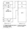
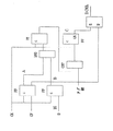
図1は、本実施例による広帯域交換システムの全体構成図である。本実施例では、広帯域ホスト交換機(HOST:Broadband Host Switch)1には、加入者端末装置が直接接続されるほか、広帯域遠隔回線集線装置(BRLC:Broadband Remote Line Concentrator) 2、広帯域遠隔交換装置(BRSU:Broadband Remote Switching Unit)3等が接続され、これらの装置に加入者宅内装置(CPE:Customer Premises Equipment) 4が接続される。このような構成により、経済的な広帯域交換システムを構築することが可能となっている。
1.2 本実施例が提供するインタフェース及びサービス
次に、本実施例が対象とする各種インタフェースについて列挙する。
1.2.1 加入者インタフェース(Subscriber Interfaces)
1.2.1.1 光ファイバインタフェース
・B−ISDN (広帯域サービス統合ディジタルネットワーク) のユーザネットワークインタフェース(UNI) を提供する156Mbps インタフェース。
・B−ISDNのUNI を提供する622Mbps インタフェース。
1.2.1.2 メタリックインタフェース
・SMDS(Switched Multi−Megabit Data Services)、フレームリレー、サーキットエミュレーション等の加入者ネットワークインタフェース(SNI) を提供する1.5Mbps インタフェース。
・B−ISDNのUNI 、及び、SMDS、フレームリレー、サーキットエミュレーション等のSNI を提供する45Mbpsインタフェース。
1.2.2 ネットワークインタフェース
・B−ISDNのネットワークノードインタフェース(NNI) を提供する622Mbps 光ファイバインタフェース。
・B−ISDNのNNI を提供する156Mbps 光ファイバインタフェース。
・B−ISDN、SMDS、フレームリレー等のNNI を提供する45Mbpsメタリックインタフェース。
・フレームリレーのNNI を提供する1.5Mbps メタリックインタフェース。
1.2.3 サービス
本実施例が対象とする広帯域交換システムは、以下に示されるようなサービスを提供することができる。
・コネクション型ATM 高速データサービス。
・スイッチトマルチメガビットデータサービス(SMDS)に基づくコネクションレス高速データサービス。
・フレームリレーサービス。
・サーキットエミュレーションサービス。
1.3 システム構成
次に、本実施例のシステム構成について説明する。
1.3.1 広帯域交換機アーキテクチャ
図2に、本実施例による広帯域交換システムのバリエーションを示す。
広帯域交換機の基本構成は、ATM 加入者スイッチ(ASSW)モジュールである。ASSWモジュールは、冗長構成を有する10Gbps (ギガビット/秒) のATM スイッチングモジュール構造、2重化構成の交換機プロセッサ、種々の加入者インタフェース装置及びネットワークインタフェース装置を含む。単一のASSWモジュールは、スタンドアローン広帯域交換機として配置することができる。
ATM インターコネクションスイッチ(AISW)は、単一のASSWの容量以上の大規模容量スイッチとして有用である。AISWは、より大規模な広帯域交換形態の要求に対して、統合されたASSW間接続形態を提供する。大規模なオフィスを構成するために、多くのASSWモジュールをAISWによって相互接続し、160Gbps に達する容量を実現することができる。多くのASSWモジュールがAISWにより相互接続される大規模な構成においては、完全なサービスを提供できる広帯域遠隔交換装置(BRSU)として機能させるために1つ以上のASSWを遠隔配置させることができる。
また、ASSWは、広帯域遠隔回線集線装置(BRLC)に対するホスト交換機として機能させることもできる。
1.3.2 スイッチトマルチメガビットデータサービス(SMDS)
図3に、本実施例が対象とする広帯域交換機でのSMDSの実現方式を示す。
加入者ネットワークインタフェース(SNI) としては、OC−3C 及びDS1/DS3 という大きく分けて2つのタイプのインタフェースを使用することができる。前者は156Mbps の光ファイバインタフェースであり、後者は1.5Mbps/45Mbpsのメタリックインタフェースである。光ファイバインタフェースは、加入者回線上に、SMDS加入者装置と他のB−ISDN装置を混在させることができる。メタリックインタフェースは、SMDS専用のインタフェースとして規定される。本実施例が対象とする広帯域交換システムは、SMDS加入者ネットワークインタフェースを直接に扱うことができる。
SMDSは、ATM に良く適合するが (SMDSのセルフォーマットはATM のそれに類似する) 、SMDSは、SMDSメッセージハンドラ(SMDS−MH) と呼ばれる特別なメッセージ処理装置を使用する。SMDS−MH は、アドレススクリーニング、メッセージルーティング、グループアドレッシング (ポイント対マルチポイント接続) 、不当メッセージチェック等の、様々なSMDS特有のサービスを提供する。SMDSは、コネクションレスサービスであるため、SMDS−MHは、メッセージ毎及びセル毎の様々なサービスを提供する。このサービスは高速性が特徴であるため、ほとんどのサービスは、ソフトウエアではなくハードウエアによって提供される。
2.本実施例が対象とするハードウエアの説明
2.1 スモールホスト用ATM ネットワーク
図4に、本実施例が対象とする広帯域交換システムの代表的なハードウエア構成を示す。この図は、スモールホスト用ATM ネットワークを対象とする。
2.1.1 ATM 加入者スイッチ(ASSW)
ASSWは、種々のタイプの加入者に対するポート (加入者インタフェース) と、ネットワークインタフェースを提供する。加入者インタフェースには、SMDSにおける加入者−ネットワークインタフェース(SNI) 、フレームリレーにおけるユーザ−ネットワークインタフェース(UNI) 、及びB−ISDN ATM UNIが含まれる。ネットワークインタフェースには、フレームリレー、SMDS、及びB−ISDNにおけるネットワーク−ネットワークインタフェース(NNI) と共に、SMDSにおけるインターエクスチェンジキャリアインタフェース(ICI) 及びインタースイッチングシステムインタフェース(ISSI)が含まれる。加入者インタフェースは、また、サーキットエミュレーションにも適用することができる。
図5に、ASSWにおけるポート構成を示す。
2.1.2 ASSWにおける加入者及びネットワークインタフェース
加入者・ネットワークインタフェースは、いくつかのタイプのシェルフとして構成され提供される。これらのシェルフには、ATM DS−1シェルフ(ADS1SH)、加入者インタフェースシェルフ(SIFSH) 、及びファイバインタフェースシェルフ(FIFSH)がある。
2.1.2.1 加入者インタフェースシェルフ(SIFSH)
図6に、加入者インタフェースシェルフ(SIFSH) の構成を示す。
加入者インタフェースシェルフ(SIFSH) は、必要な電源、共通カード、及び種々のタイプのDS3 又はOC−3C インタフェースカードを8枚まで装着するためのマウントスロットを提供する。これらのインタフェースカードには、ATM OC−3C カード群(OC3CPG)、ATM DS−3カード群(ADS3PG)、フレームリレーDS−3カード群(FDS3PG)、サーキットエミュレーションDS−3カード群(CDS3PG)、及びADS1SHインタフェースカード(ADSINF)などがある。ATM DS−3カードは、ATM とSMDSの両方のインタフェースを提供する。
ATM OC−3C カード群(OC3CPG)は、B−ISDN UNIに接続されるATM 機器から受信された情報に対するATM セル交換を提供する。
DS−3カード群の機能は、回線速度がDS−1レートではなくDS−3レートで提供されるという点を除いて、ADS1SHに装着されるDS−1カード群と同様である。
また、SIFSH は、ADS1SHインタフェースカード(ADSINF)を扱うこともできる。ADSINFカードの組 (1組は2カード) のそれぞれは、4シェルフのADS1SHをインタフェースする。1つのSIFSH あたりでは、16シェルフのADS1SHがインタフェースされる。それぞれのADS1SHは8個のDS−1ポートを扱うことができ、また、後述するように2つのSIFSH シェルフをデイジーチェーン接続させることができるため、1組 (1組は2シェルフ) のSIFSH が接続されるポートにおいて、256個のDS−1カードを扱うことができる。
2.1.2.2 ATM DS−1シェルフ(ADS1SH)
図7に、SIFSH に対するADS1SH接続を示す。
ATM DS−1シェルフ(ADS1SH)は、種々のDS−1インタフェースカードを収容する。これらのカードには、フレームリレーDS−1カード群(FDS1PG)、SMDS DS−1 カード群(SDS1PG)、及びサーキットエミュレーションDS−1カード群(CDS1PG)がある。
フレームリレーDS−1カード群は、長いフレームリレーメッセージの個々のATM セルへの分割機能、セル交換のための必要なタグと共に仮想呼識別子を付与する機能等を提供する。また、このカード群は、ATM スイッチからセルを受信し、それらのセルからフレームリレーフォーマットを組み立てする機能を提供する。この適応処理は、分割/組み立て機能と呼ばれる。この機能は、ATM セル交換技術をフレームリレートラヒックに適用することを可能にする。
SMDS DS−1 カード群は、同様の機能を提供する。この機能は、データをセルの大きさのデータユニット列として提供するものである。
サーキットエミュレーションDS−1カード群は、完全同期トラヒックであるチャネルから受信された情報を、連続したセルに格納する機能を提供する。この機能も、ATM ネットワーク内を交換してゆくことができるように、情報をATM セル列に分解する。また、サーキットエミュレーションカード群は、情報信号がATM ネットワークから離れる際に、信号タイミングを回復させる機能も提供する。
ADS1SHシェルフは、必要な電源、共通カード、及び3タイプのDS−1カードを8枚まで装着するためのマウントスロットを提供する。このシェルフの出力は、加入者インタフェースシェルフ(SIFSH) にマウントされているADS1SHインタフェースカード(ADSINF)に接続される (図7参照) 。
2.1.2.3 ファイバインタフェースシェルフ(FIFSH)
ファイバインタフェースシェルフ(FIFSH) は、必要な電源と、OC−12Cインタフェースを4枚までマウントするためのスロットを提供する。それぞれのインタフェースには、ATM OC−12Cカード群(OC12PG)、及びファイバインタフェースカード(FIFCPG)の組 (1組は2枚) がある。
2.1.3 ASSW ATMスイッチモジュール
ATM スイッチモジュールは、最大で 10Gbps(ギガビット/秒) の容量を有するものとして構成することができる。このモジュールは、16ポートまでのトラヒックの出入口を供給する。スイッチ構造は、上り用と下り用の2つの分離された部分として構成される。加入者・ネットワークポートからやってくるトラヒックは、上り方向トラヒックを提供するATM ネットワーク上の16個のポートに供給される。加入者・ネットワークポートへ戻ってゆくトラヒックは、下り方向トラヒックを提供するATM ネットワーク上の16個のポートから取り出される。そのようなトラヒックは、ASSWに接続される種々の加入者・ネットワークインタフェースに対して送受信される。いくつかのネットワークポートは、ネットワークにおける一般的なシグナリング処理及びSMDSのためのメッセージ処理を行うサービス装置により使用される。図8に、ASSWを中心とするネットワークの構成例を示す。
2.1.3.1 ATM スイッチングシェルフ (ASSWSH)
ATM スイッチングシェルフ (ASSWSH) は、ATM スイッチングネットワーク全体と関連する電源を収容する。このスイッチングネットワークは、10Gbpsを提供する4×4のノンブロッキングスイッチとして構成される。このスイッチングネットワーク上のそれぞれ2.5Gbps の容量を有する4つのポートのそれぞれは、4つの関連するセルルーティングを多重するためのマルチプレクサカードを有する。従って、1つのポート内の1つのセルルーティングの容量は、2.5Gbps/4=622Mbps となる。この結果、スイッチングネットワークには、全体として、それぞれ622Mbps の容量を有する16組の入力が供給されることになる。
ATM スイッチモジュールは、常に同じ4×4のサイズを有するように構成される。
4つのネットワークポートのそれぞれを接続するための1組のマルチプレクサカードは、独立の装置構成とされる。
また、ASSWSHは、2組の共通カードと、タイミング生成用の1組のセルクロックジェネレータカード(CELCLK)と、プロセッサ装置の接続用の1組のパラレルATM インタフェースカード(PIAINF)を含む。
2.1.3.2 デイジーチェーン構成
加入者/ネットワークインタフェースを供給する前述したシェルフ群は、ATM スイッチングネットワーク上の16個のポートのそれぞれに接続される1つのシェルフによって、そのATM スイッチングネットワークに接続することができる。その1つのシェルフが622bpsの容量を完全に供給していない場合には、そのシェルフを他のもう1つのシェルフとデイジーチェーンさせることができる。デイジーチェーンでは、第1番目のシェルフがスイッチポートに接続され、第2番目のシェルフが第1番目のシェルフに接続される。図5に示したように、2つのSIFSH をデイジーチェーンさせることができる。このような配置は、ATM スイッチングネットワークに対する16個のポートに32個までのシェルフを接続することを可能とする。
2.1.4 ASSWにおけるその他のATM ネットワークサポート装置及びテストセル生成方式
上りスイッチ部分からのトラヒックは、2通りの方法によって下りスイッチ部分に接続させることができる。即ち、この機能は、ループバック回路又はATM インターコネクションスイッチ(AISW)によって実現される。ループバック配置は、どのようなASSW内接続をもサポートする。一方、ASSW間接続は、AISWを介した接続によってサポートされる。
2.1.4.1 ループバック用加入者インタフェースシェルフ (SIFSH)
図9に、SIFSH におけるループバック構成を示す。
SIFSH は、上りネットワークからの8個までの156Mbps の出口を下りネットワークへの8個までの156Mbps の入口に接続するための8個までのループバックカードグループ(LOOPPGA) を含む。また、このシェルフは、上記ループバックカードのための電源を内蔵する。将来的には、622Mbps のループバックカードグループを利用することができる。このカードは、156Mbps 以上の帯域幅のサービスが導入された場合に必要となる。
2.1.4.2 テストセルジェネレータ用加入者インタフェースシェルフ
図10に、SIFSH に接続されるテストセルジェネレータの構成を示す。
図10に示されるように、SIFSH は、試験に使用されるテストセルジェネレータアダプタ(TCGADPs) を内蔵できる。このTCGADPs は、ASSWの出入口上に配置されるSIFSH に内蔵される。テストセルジェネレータ(TCG) は、図10に示されるように、テストセルジェネレータシェルフ(TCGSH) 内に配置される。
2.1.5 ASSWにおけるシグナリング装置
システム上の各ポート装置のシェルフは、対応するマイクロプロセッサを有している。広帯域シグナリングコントローラシェルフ (BSGCSH) は、ASSWの広帯域コールプロセッサ (BCPR) と上述の種々のポート用マイクロプロセッサの間のシグナリング、及びB−ISDN UNIシグナリングを、処理する。
図11に、BSGCSHの構成を示す。このシェルフは、必ず配置され、電源と、共通カードと、6枚までの広帯域シグナリングコントローラカードグループ (BSGCPGA)を内蔵する。BSGCSH内のBSGCは、INFA (周辺インタフェースタイプA)及びINFT (周辺インタフェースタイプT)を介して、BCPRが接続されるシステムバス(BCPR Bus)に接続される。
2.1.6 SMDSメッセージハンドラ
SMDSメッセージ処理装置は、2つの異なるタイプのものがある。1つは、加入者SNI ポートに対応するシグナリング要求を処理し、他の1つは、ICI 及びISSIトランクポートに対応するシグナリングを処理する。
2.1.6.1 加入者メッセージハンドラシェルフ (SBMESH)
加入者メッセージハンドラシェルフ (SBMESH) は、SMDS加入者SNI ポートからのメッセージを処理する。このシェルフは、何れかのSMDS加入者SNI がASSW又はそれに接続されるBRLC上のポートに存在するならば必ず、或いは、SMDSトラヒックが加入者側のターミナルアダプタが接続されるATM UNI 設備を介して転送されてくるような場合に、用意される。
各SBMESHシェルフは、そのシェルフの容量までDS−1設備とDS−3設備を混在させてサービスを提供することができる。また、そのシェルフは、102Mbps の情報レートを有するSMDS情報を処理する。この場合、DS−3に対する最大情報レートは34Mbpsであり、DS−1に対するそれは1.17Mbpsである。また、1つのシェルフは、32SNI までを処理することができる。この基準によれば、1つのシェルフは、3本のDS−3伝送路又は32本のDS−1伝送路までを処理することができる。これらの制限に加えて、スイッチングネットワークは、1ポートあたり622Mbps までのトラヒック容量に制限される。
本実施例におけるシステムは、スイッチングネットワークの入口に対して4個のSBMESHまでをデイジーチェーン接続することができる。もし、スイッチングネットワークにSMDS DS−1 伝送路のみが接続されていると仮定すると、4つのデイジーチェーン接続されたSBMESHが接続された1つのネットワークポートは、12本までのDS−3伝送路、又は128 本までのDS−1伝送路、或いはそれらの混在形態を扱うことができる。もし、ASSWにおけるSMDSポート (トラヒック) が単一のメッセージハンドラグループのキャパシティを超えた場合には、より多くのメッセージハンドリング装置を提供するために、他の1つ又は幾つかのポートを選択することができる。
2.1.6.2 ゲートウエイメッセージハンドラシェルフ (GWMESH)
ゲートウエイメッセージハンドラシェルフ (GWMESH) は、ASSW上のSMDS ICI及びISSIポートに対するメッセージ処理及びシグナリング機能を提供する。
各GWMESHには、上述したSBMESHに対するのと同じ制限がある。SMDS ICI又はISSIがDS−3フォーマットで実現され、フル容量で運用されている場合、GWMESHに対する事実上の制限は、3本のDS−3 ICI、ISSIである。SMDS ICI又はISSIがOC−3C をフルに利用する形態で実現されている場合、1つのメッセージハンドラシェルフは、単一のOC−3C専用に使用されなければならない。本実施例によるシステムでは、スイッチングネットワークへの同一の入口に、4つまでのGWMESHシェルフをデイジーチェーン接続させることができる。この場合でもまた、トラヒックが単一のメッセージハンドラグループのキャパシティを超えた場合には、他の1つ又は幾つかのポートを追加することができる。
SMDSに対する要求が小さいオフィスでは、シェルフ毎の制限を超えず、かつ全体のトラヒックが622Mbps を超えない限りにおいて、1つ以上のSBMESHと1つ以上のGWMESHをデイジーチェーン接続させることができる。このような技術的配置は、SMDS機能に対するポート使用率を最小化する上で有用である。
2.2 広帯域遠隔交換装置(BRSU)
図12に、BRSUの主なハードウエア構成要素を示す。BRSUの構成要素は、ホスト交換機内のASSWのそれと同じである。
2.3 広帯域遠隔回線集線装置 (BRLC)
図13に、BRLCの主なハードウエア構成要素を示す。
ASSWに対して遠隔の配置で加入者インタフェースを収容する必要がある場合、広帯域遠隔回線集線装置 (BRLC) を使用することができる。BRLCは、ASSWに対して遠隔に配置され、スイッチング機能を実行する。
BRLCは、本質的には、顧客群からのトラヒックを集線し、それをASSW (1つ以上のアンビリカルリンクによって接続されている) に配信する。
BRLCは、ASSWにおけるものと同様のタイプの加入者/ネットワーク接続入力ポートを有する。コールプロセッサは存在しないが、ポートとアンビリカルリンクとの間のネットワークを交換するある種の汎用的な装置を有している。
図14に、BRLCにおける接続構成を示す。
2.3.1 加入者入力ポート
種々の加入者インタフェースが、BRLCのポートに接続されている。これらのポートは、種々のタイプのシェルフ装置手段により実現されている。それらには、図14に示されるように、ASSWにおいて実現されているものと同様の、ATM DS1 シェルフ(ADS1SH)及び加入者インタフェースシェルフ(SIFSH) などが含まれる。BRLC全体の最大容量は622Mbps であるため、ファイバインタフェースシェルフ(FIFSH) はBRLCでは使用されない。
ATM DS1 シェルフ(ADS1SH)は、種々のタイプのDS−1インタフェースカードグループを収容する。これらには、フレームリレーDS−1カードグループ(FDS1PG)、SMDS DS−1 カードグループ(SDS1PG)、及びサーキットエミュレーションカードグループ(CDS1PG)が含まれる。ADS1SHについては、2.1.2.2で説明した。
加入者インタフェースシェルフ(SIFSH) は、種々のネットワークインタフェースカードを収容する。SIFSHは、ATM OC−3Cカードグループ、種々のDS−3カード、又はATM DS−1シェルフインタフェースカード(ADSINF)を収容できる。SIFSHについては、2.1.2.1で説明した。
2.3.2 アンビリカル装置
BRLCとそれに対するサーバであるASSWとの間のアンビリカルリンクは、ADS3PGAを使用するDS−3設備又はOC3PGAを使用するOC−3C設備として構成することができる。また、このアンビリカルリンクは、OC12PGAカードグループを使用した単一のOC−12C としても提供することができる。BRLCの容量は622Mbpsに制限されているため、アンビリカルリンクの最大構成は、1本のOC−12C 又は4本のOC−3Cである。DS−3を使った最大構成では、12組のDS−3設備が提供され、約622Mbps のトラヒックを処理できる。任意のBRLCからの全てのアンビリカルリンクは、同一のASSWに接続されなければならない。
DS−3又はOC−3カードが使用される場合、最小構成として、最初の4枚のカードをRMXSH の予約スロットにマウントすることができる。カードの枚数が4枚を超えた場合、更に8枚のカードをマウントできるSIFSHを追加することができる。もし、OC−12Cにおいて必要ならば、FIFSHシェルフを使用することができる。SIFSH及びFIFSHについては、既に説明した。
2.3.3 ネットワーク装置
BRLCは、スイッチングネットワーク或いはASSWを有しない。この結果、ネットワークスイッチングシェルフ及び同期化シェルフは必要とされない。しかし、加入者ポート及びアンビリカルリンクを供給する種々のシェルフ装置は、ネットワーク装置にインタフェースされる必要があり、また、それらのシェルフ装置はネットワーク装置の所定の機能を要求する。このようなことから、BRLCは、ネットワークの代わりに機能するシェルフ装置を必要とする。この機能は、RMXSH シェルフによって実現される。
遠隔多重シェルフ(RMXSH) は、ネットワーク代用機能及び多重装置としての機能を提供する。このシェルフは、加入者インタフェースからのATM セルを受信して、提供されている種々のアンビリカルリンクに多重する。このシェルフは、また、多重機能に対するタイミングを確立しそれに基づく処理を実行する。
RMXSH シェルフは、その機能を実現するために、クロック回路と多重装置を有する。そして、このシェルフは、電源と共に、1組の遠隔多重タイミングジェネレータカードグループ(RMXTPG)、1組の遠隔多重ハイウエイカードグループ(RMXHPG)、及び1組の遠隔多重コントローラカードグループ(RMXCPG)を常に装備している。
3.本実施例で実現される機能
3.1 概説
この章では、本実施例が対象とする広帯域交換システムの構成要素について説明する。これらの構成要素は、以下の4つのカテゴリに分類される。
・ホスト交換機
・広帯域遠隔交換装置(BRSU)
・広帯域遠隔集線装置(BRLC)
・加入者宅内装置
3.2 ホスト交換機
ホスト交換機は、以下のような構成要素から構成される。
・ATM 加入者スイッチ(ASSW)
・ATM インターコネクションスイッチ(AISW)
・広帯域メインプロセッサ(BMPR)
・メンテナンス/オペレーションサブシステム(MOS)
・光リングバス
ホスト交換機は、更に以下の2つのタイプに分類される。
・スモールホスト交換機
・ラージホスト交換機
図15に、スモールホスト交換機とラージホスト交換機の構成を示す。ASSWが構成の基本となる。スモールホスト交換機は、1つのASSW、BMPR、及びMOS から構成される。ラージホスト交換機は、複数のASSWと、1つのAISWと、1つのBMPRと、1つのMOS から構成される。ラージホスト交換機において、AISWは複数のASSW間を接続する。スモールホスト交換機からラージホスト交換機への移行は、サービスを中断させることなく行うことができる。
光リングバスは、広帯域交換システム及び狭帯域交換システムが1つのシステムに統合される場合に使用される。
なお、本実施例は、主にスモールホスト交換機を対象として説明している。
3.3 ATM 加入者スイッチ (ASSW)
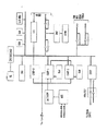
ATM 加入者スイッチ(ASSW)は、広帯域交換システムにおける基本的な構成要素である。図16に、ASSWの構成を示す。ASSWは、10Gbpsの容量のスループットを有し、以下の構成要素から構成される。
・ATM スイッチモジュール(ASM)
・加入者/ネットワークインタフェース
・広帯域シグナリングコントローラ(BSGC)
・SMDSメッセージハンドラ(SMDS−MH)
・広帯域コールプロセッサ(BCPR)
3.3.1 ATM スイッチモジュール(ASM)
広帯域交換機におけるATM スイッチモジュール(ASM) は、シングルステージ又はマルチステージのセルフルーティングモジュール(SRM) によって構成されている。SRMは、2.5Gbpsのリンクスピードを有するN×Nのスイッチングマトリックスにより構成される。図17に、SRM の原理を示す。SRM に流入されたATM セルは、各セルに付加されているタグに従って出力ポートへルーティングされる。
図18に、ASSWにおいて使用される4×4のSRM の構成を示す。4×4のSRM において、セルは、4つの入力ポートと4つの出力ポートとの間で交換される。SRMは、特別に設計されたバイポーラCMOS大規模集積回路(VLSI)によって構成される。このSRM は、2×2のスイッチマトリックスを含む。それぞれのクロスポイントは、2.5Gbpsのスイッチング容量を有する。
セルスイッチングの原理は次の通りである。ここでは、入力ハイウエイHW0 から出力ハイウエイHW2 へのセルスイッチングを例として説明する。
まず、各セルには、タグが付加されている。
例えば、HW0 から入力されたセルには、タグ2が付加されると仮定する。それぞれのスイッチングエレメントは、タグ値をチェックし、出力ポート番号に等しいタグを有するセルのみをスイッチする。図18の例では、スイッチングエレメントSW02が該当する。もし、複数のセルが1つの出力ポートに出力される場合には、アクセス制御機構が、各クロスポイント内のバッファを用いることにより、セルの競合を回避する。
図19に、仮想チャネル識別子コンバータ(VCC) の位置を示す。タグは、加入者/ネットワークインタフェースなどの周辺装置に配置されているVCC により、セルに付加される。VCC は、各セルのためのタグ値を特定する。タグ値は、呼接続における呼設定フェーズ又は半固定接続の設定フェーズにおいて処理されるソフトウエアテーブルに従って設定される。
タグ情報は、デマルチプレクサにおいても使用される。タグは、ATM スイッチモジュール及び周辺装置内のデマルチプレクサの出力ポートを特定する。
図20に、ASSWのATM スイッチモジュールの構成を示す。ASSWのATM スイッチモジュールは、上り用と下り用の2つに分離された各4×4のSRM により構成される。加入者/ネットワークインタフェース、広帯域シグナリングコントローラ(BSGC)、SMDSメッセージハンドラ(SMDS−MH) などの周辺装置インタフェースは、622Mbps の容量を有する。全ての加入者/ネットワークインタフェースは、ATM スイッチモジュールの一方の側に集合させられる。ATM スイッチモジュールの他方の側には、ASSW内トラヒックをルーティングするループバックリンクが配置される。AISWが使用されるラージホスト交換機においては、AISWのインタフェースがループバックリンクに置き換えられる。
3.3.2 加入者/ネットワークインタフェース
図21に、本実施例の加入者インタフェース(SNI )/ネットワークインタフェース(ICI/ISSI)を説明する構成図を示す。同図に示すように、加入者インタフェース/ネットワークインタフェースとして以下の3つの速度を提供する。
・高速:622 Mbps光インタフェース
・中速:156 Mbps光インタフェース,45 Mbps メタルインタフェース
・低速:1.5 Mbpsメタルインタフェース
上記3つの速度のインタフェースに対しては、それぞれ異なったシェルフが使用される。低速インタフェースの信号は、いったん8 Mbpsリンクに多重化された後に、中速インタフェースのシェルフに収容される。中速インタフェースのシェルフは、輻輳を考慮し、2シェルフまでイモヅル式に接続することができる。加入者インタフェースとネットワーク・インタフェースは共通であり、それら2つのシェルフを同一シェルフで構成できる。ただし、これらのシェルフはトラフィック集中が起こるので、加入者側とネットワーク側で異なるグレイドのサービスを要求するのであれば、それらシェルフを分離する必要がある。
加入者インタフェース/ネットワークインタフェースとしては、以下の4つのタイプに分類することができる。
・B−ISDN(ATM)
・SMDS
・フレーム・リレー
・サーキット・エミュレーション
上記各サービスに対して異なるインタフェース・カードが使用されるが、シェルフは共通とすることができる。これらインタフェース・カードは、サーキット・エミュレーションを除いて、加入者側とネットワーク側で異なる。
3.3.3 広帯域シグナリング・コントローラ(BSGC)
BSGC(Broadband Signaling Controller)はATM インタフェースとのHDLC(HighLevel Data Link Procedure)ハンドラである。図22はASSW内におけるBSGCの位置を示す図である。BSGCは、INF (Interface)経由でBCPR(Broadband Call Processor)によって制御され、B−ISDN UNIおよびB−ISDN NNIのためのLAPD(Link Access Procesure D−channel)もしくはCCS7シグナリングを提供する。BSGCは、BCPRとBRLC(Broadband Remote Line Concentrator)との間の通信と行うとともに、BCPRとSNI インタフェース装置との間の内部通信も行う。
3.3.4 メッセージ・ハンドラ(SMDS)
SMDS−MH (SMDSメッセージ・ハンドラ)は、アドレス・スクリーニング、メッセージ・ルーティング、グループ・アドレス処理(ポイント・トゥ・ポイント通信)、異常メッセージチェック、課金処理、データ・コレクション等のSMDS対応機能を提供する。図23は、ASSW内におけるSMDS−MH の位置を示した図である。この実施例では、SMDS−MH として、以下の2つのタイプを示す。
・SBMH(Subscriber Message Handle :加入者メッセージ・ハンドラ)
・GWMH(Gateway Message Handle :ゲートウェイ・メッセージ・ハンドラ)
SBMHは、SNI のためのメッセージ処理を行う。一方、GWMHは、ICI やISSIなどのスイッチ間インタフェースのためのメッセージ処理を行う。
3.3.5 広帯域コール・プロセッサ(BCPR)
図24にBCPR(Broadband Call Proseccor)の構成を示す。BCPRは、全てのSNIのための呼制御を行う。BCPRは、以下の各ユニットを含む。
・CPU
・メインメモリ
・イーサネット・インタフェース
・INF
イーサネット・インタフェースは、スモールホスト交換機内において、BCPRとBMPR(Broadband Main Processor)との間の通信に使用される。INF は、ATM スイッチモジュール、BSGC、SMDS−MH 等の各種ASSW内の装置とBCPRとの間のインタフェースを提供する。
3.3.6 メンテナンス・アンド・オペレーション・システム(MOS )
MOS(Maintenance and Operation System) は、各種メンテナンス及びオペレーションを行う。図25にMOS の構成を示す。MOS は以下の各ユニットを含む。
・アラーム・パネル・ユニット
・アラーム・コントロール・ユニット
・オペレーション・アンド・メンテナンス・プロセッサ
広帯域スイッチのみのシステムでは、MOS は、イーサネット・インタフェースを介して直接BMPRに接続され、BMPRとの連携動作によってオペレーションおよびメンテナンス機能を提供する。狭帯域および広帯域スイッチからなるシステムでは、MOS は、狭帯域および広帯域スイッチング・システムに光リング・バスで接続され、広帯域システム用BMPRおよび狭帯域システム用メイン・プロセッサとの連携動作によってオペレーションおよびメンテナンス機能を提供する。
3.3.7 オペレーション・アンド・メンテナンス・プロセッサ(OMP )
OMP(Operation and Maintenance Processor)は、本実施例のフロントエンド・プロセッサである。OMP は、システム管理・制御、およびラインやトランクの試験に加えて、本システムに複数のOSを接続する。OMP のハードウェア構成(図26参照)を以下に示す。
・CPU (メモリを含む)、ディスクドライブ、フロッピ・ディスクドライブ
・CRT ディスプレイ(GUI 使用)
・キーボード
・マウス
・ハードディスク
・カートリッジテープドライブ
・非同期通信サーバ
・プリンター
・X.25インタフェース
3.3.8 システム・インテグレーション・プロセッサ(SIP )
SIP(System Integration Processor) は、OMP を光リングバスに接続する場合に使われる。1つのOMP がSIP を介して光リングバスに接続されると、他のアプリケーション(狭帯域、広帯域、その他)で処理可能となる。
3.4 広帯域遠隔集線装置(BRLC)
BRLC(Broadband Remote Line Concentrator)の構成を図27に示す。BRLCは、ホスト交換機から遠隔地に加入者インタフェースを提供する。BRLCは、トラフィック集線を行うが、遠隔地での交換は行わない。オペレーション及びメンテナンス機能は、基本的にはホスト交換機から提供される。ネットワーク・インタフェースは、ホスト交換機とのアンビリカルからなる。このアンビリカルが切れた場合、BRLCは、スタンドアロンとして動作することはできない。
3.5 広帯域遠隔交換装置(BRSU)
BRSU(Broadband Remote Switching Unit) の構成を図28に示す。BRSUは、ホスト交換機からの遠隔地において、加入者インタフェース、ネットワーク・インタフェース、交換機能を提供する。BRSUは、AISWか設けられたラージ・ホスト交換機から制御される。オペレーションおよびメンテナンス機能は、基本的にはホスト交換機から提供されれるが、一部機能はBRSU自身が有する。BRSUは、ホスト交換機と同じ加入者インタフェース/ネットワークインタフェースを提供する。ホスト交換機とのアンビリカルは、BRLCの場合のそれと類似するが、BRSUでは、もしそのアンビリカルが切断された場合でもスタンドアロンとして動作し、スイッチ間サービスを提供しつづけることができる。
3.6 SMDSの実施態様
SMDSは、コネクションレス高速パケットデータサービスである。SMDSに関する装置を図29に示す。SMDSのトラフィックは、DS1/DS3 インタフェース部とSMDSメッセージ・ハンドラ部で処理される。
・DS1/DS3 インタフェース部
・加入者インタフェース/ネットワークインタフェースのレベル1(物理レイヤ)の終端
・SNI level−2 のATM レイヤの終端
・パフォーマンス・モニタ
・メッセージ・ハンドラ
・SNI level−2 のSAR の終端
・SNI level−3 機能(フォーマット・チェック、アドレス・スクリーニング、ルーティング、フロー制御)
・データ・コレクション(ネットワーク・トラフィック管理、ネットワーク・データコレクション、課金)
SMDSは、ターミナル・アダプタを介して、B−ISDN(ATM) 加入者インタフェースを用いて構成することができる。この場合、DS1/DS3 インタフェースをターミナル・アダプタで提供する。
レイヤ構造のSNI のプロトコルを図30に示す。また、SMDSは、図31に示すレイヤ構成を採用している。さらに、図32に、SMDSシステムにおけるセルのルーティングを示す。
フロー制御は、以下の2ヵ所で実行される。
・DS1/DS3 インタフェース部でのユーザ・パラメータ・コントロール(UPC)
・GWMHでのトラフィック・シェイピング
3.7 トラフィック管理
トラフィック管理は、以下のメカニズムによって実現される。
・呼受付制御
・使用量制御
・セル・ルーティングの優先度
3.7.1 呼受付制御
サービスの要求品質(たとえば、セル廃棄率やセル伝送遅延)を保証するために、システムは帯域を管理し、呼の受け付け時点で各呼ごとに要求された帯域が守られているこチェックする。呼に対する処理は、ピーク値、平均値、およびサービスの要求品質等に従って実行する。
システム内での帯域は、以下の3地点で仮想パス(Virtual Path)ごとに管理される。
・加入者インタフェース
・ネットワーク・インタフェース
・システム内の622 Mbps
上記仮想パスの容量は、以下の2点で管理される。
・各呼のクラスの帯域(W1):各呼のクラスに対して割り当てられ、管理される帯域
・共通帯域(W2):呼のクラスとは無関係に割り当てられ、管理される帯域
なお、W2領域は、W1からオーバーフローした呼、W1において設定されていない呼によって利用される。
3.7.2 ユーザ・パラメータ・コントロール(UPC )
UPC(User Parameter Control) は、各呼の実際のトラフィックを管理する。上記設定値を越えた呼が検出された場合には、システムは、その呼のセルを廃棄するか、そのセルに対して設定値を越えたことを示すタグを付与する。
UPC は、仮想チャネル(VC)、仮想パス、またはそれら両者に対して実行される。加入者線に対しては、UPC は加入者インタフェース部において仮想チャネル毎に行われる。上記設定値を越えたセルに対しては、以下の処理がなされる。
・B−ISDN:廃棄または設定値を越えたことを示すタグの付与
・SMDS :廃棄
ネットワーク側(たとえば、他の交換機やBRSU/BRLC とのインタフェース)では、ネットワーク・インタフェース部において、各仮想パス(または仮想チャネル)ごとに実行される。
3.7.3 セル・ルーティングの優先度
セル・ルーティングの優先度の制御は、システム内のMUX/DMUX部およびATM スイッチにおけるバッファで行われる。その制御は、以下に示す2つのスレッシュホルド値を用いてキュー(待ち行列)で実現される。
・重要でない加入者セルを廃棄するためのスレッシュホルド値
・CLP(cell loss priority) =1のセルを廃棄に関するスレッシュホルド値
3.8 データ・コレクション
本実施例のシステムでは、以下のデータを収集する。
・AMA (Automatic Message Accounting)データ
・パフォーマンス・モニタリング・データ
・ネットワーク・トラフィック管理データ
・NDC (ネットワーク・データ・コレクション)データ
AMA データは、例えば、BMPRまたはSIP の記憶装置に格納され、OSに転送される。
パフォーマンス・モニタリング・データは、15分間隔または24時間間隔で収集される。このデータは、BMPRの記憶装置に格納され、OSから要求があった場合に、OMP を介してOSに転送される。
ネットワーク・トラフィック管理データは、輻輳の検出・通知のためにに使用され、その輻輳レベルが所定のスレッシュホルド・レベルを越えたときに収集される。また、所定間隔(5分)での収集も行われ、OMP を介してリアルタイムでOSに転送される。
NDC データは、長期的な予測のために使用される。このデータは、OSからの要求があったときに、OMP を介してBMPRの記憶装置に格納される。
4.その他
以上説明した本実施例の全体構成のうち、例えば図8に示されるDS3−SMDSインタフェース(DS3) 、SIFSH 、ASSWSH、SBMESH、GWMESH、及びBSGCSHの詳細について、以下のパート2〜7で説明する。その後に、パート8において、本発明に特に関連する構成及び機能等について説明する。なお、DS1−SMDSインタフェース(DS1) については、伝送速度が異なるだけで、基本的な機能はDS3−SMDSインタフェースと同様であるため、その詳細については省略する。
【0006】
<パート2>
パート2では、DS3−SMDSインタフェースの詳細について説明する。
1.概略説明
DS3−SMDSインタフェースは、DS3 伝送路を使用してSMDSサービスを行うための回線インタフェースとして使用される。また、DS3−SMDSインタフェースは、BRLC(Broadband Remote Line Concentrator:広帯域遠隔回線集線装置) を接続してアンビリカルリンクを実現するためのインタフェースとして使用される。
SMDS(Switched Megabit Data Service) とは、高速のコネクションレスデータサービスの一種であり、LAN とLAN とを接続してデータを交換するサービスとして機能することを期待されている。
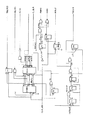
図33は、DS3−SMDSインタフェースを中心としたシステム構成の概略を示す図である。また、図34は、交換機1にBRLC2が接続される構成を示した図である。
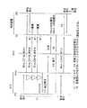
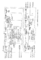
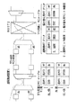
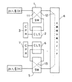
図33に示されるDS3−SMDSインタフェース1、3は、SIFSH(Subscriber Interface Shelf) 6に搭載される。また、図34に示されるDS3−SMDSインタフェース3 (図ではDS3−ATM と記載されている) は、交換機1内のSIFSH 7又はBRLC2内のRMXSH(Remote Multiplexer Shelf) 7に搭載される。DS3−SMDSインタフェースは、それがSIFSH に搭載される場合、最大で8リンク分までSIFSH に搭載することができる。SIFSH は、ATM スイッチとのインタフェース部分である2重化された構成を有する共通部(SIFSH−COM or SIFSH Common) と、1重化された構成を有する回線個別部より構成される。DS3−SMDSインタフェースは、回線個別部に搭載される。また、SIFSH は、最大で2シェルフまでカスケードに接続され、4:1の集線化を行う。
図33において、DS3−SMDSインタフェース1は、SMDSサービスを提供するためのDS3 伝送路2上のDS3 レイヤーを終端し、DS3 伝送路2から入力されるDS3 フレームのインフォメーションペイロード部に収容されているPLCPレイヤーのフレームを取り出す。そして、DS3−SMDSインタフェース1は、取り出したPLCPレイヤーのフレームからL2プロトコルデータユニット(L2−PDU)を抜き出し、L2−PDUヘッダのHCS(HEC)チェックを行った後、53オクテットのL2−PDRU からATM スイッチ5内で処理可能な54オクテットのATM セルへの変換(53/54オクテット変換) を行い、そのATM セルを、622Mbps(メガビット/秒) の伝送速度を有する高速上りハイウエイ(Upward Highway)に多重して、ATM スイッチ3に送出する。
逆に、DS3−SMDSインタフェース1は、ATM スイッチ3から伸びている高速下りハイウエイ(Downward Highway)から分離したATM セルから、上述した手順と逆の手順によりDS3 フレームを組み立て、それをDS3 伝送路2に送出する。
一方、図34に示されるように、DS3 伝送路4にBRLC(Broadband Remote Line Concentrator:広帯域遠隔回線集線装置) が接続される場合には、DS3−SMDSインタフェース3は、アンビリカルリンクを実現する。この場合、図34において、交換機1内のDS3−SMDSインタフェース3は、DS3 伝送路4によってBRLC2内のDS3−SMDSインタフェース5と接続される。
2.回線インタフェースの説明
2.1 DS3 回線インタフェース
2.1.1 ペイロードマッピング
DS3 回線インタフェースにおいて、ATM スイッチ側のデータフォーマットであるATM セルと伝送路側のデータフォーマットであるDS3 フォーマットとの間のマッピングを、図35に示す。
2.1.2 DS3 フレームフォーマット
図33において、DS3−SMDSインタフェース1は、伝送路2上のフレームフォーマットである図35に示される非同期DS3 フレームフォーマット(Asynchronous DS3 FRAME FORMAT)(M13 Format) を終端する。このフレームフォーマットの更に詳細な構成を、図36に示す。
1つのマルチフレーム(Multiframe)は、7つのサブフレーム(Subframe)によって構成される。1つのサブフレームは更に、それぞれ85ビットからなる8個のブロックによって構成される。1つのブロック内の85ビットのうち、最初の1ビットはDS3 オーバーヘッド部であり、残りの84ビットが情報ペイロード部(INFO.PAYLOAD)である。
DS3 回線インタフェースにおいては、44.736MHz のビットレートで、1つのマルチフレームが、106.4 μsec(マイクロ秒) の周期で伝送される。
3.PLCPフレームフォーマット
3.1 DS3 PLCPフレームフォーマット
図37に、図35に示されるPLCPレイヤ(PLCP LAYER)に対応するDS3 PLCPフレームのフォーマットを示す。DS3 PLCPフレームは、図35に示される非同期DS3 フレームフォーマットにおけるサブフレーム内のインフォメーションペイロード(INFO.PAYLOAD)を使って伝送される。この場合、フレーム内の各オクテット(octets)は、4ビットからなるニブル(nibble)という単位で、順に伝送される。なお、図35に示されるDS3 フレームフォーマットのマルチフレーム又はサブフレームの先頭とDS3 PLCPフレームの先頭は、同期している必要はない。
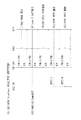
4.DS3−SMDSインタフェース L2−PDUフォーマット
4.1 DS3−SMDS L2−PDU フォーマット
図38に、図35又は図37のPLCPフレームに挿入されるDS3−SMDS L2−PDU(L2 Protocol Data Unit)のフォーマットを示す。図38又は図35に示されるように、DS3−SMDS L2−PDU は、7オクテット(octets)のヘッダ(HEADER)と、44オクテットのインフォメーションフィールド(INFO.FIELD)、及び2オクテットのトレーラ部(TRAILER) によって構成されている。
まず、図38のヘッダ(HEADER)内のアクセスコントロールフィールド(Access Control 、又は図35のACF)は、DS3−SMDSインタフェースが終端する伝送路上におけるL2−PDUの伝送状態を検出するために使用される。DS3−SMDSインタフェースが終端する伝送路が、SNI(加入者−ネットワークインタフェース。例えば図33の伝送路2) である場合と、NNI(ネットワーク−ノードインタフェース。例えば図33の伝送路4) である場合のそれぞれ、並びに上り伝送路及び下り伝送路のそれぞれにおけるアクセスコントロールフィールドの内容を、図39に示す。
図39において、DS3−SMDSインタフェースが終端する伝送路がSNI である場合には、BUSYビットは、そのビットが含まれるL2−PDUが情報を含んでいるか否かを示す。また、DS3−SMDSインタフェースが終端する伝送路がSNI で、かつその伝送路が上り伝送路(ATMスイッチ側に入力する伝送路) である場合には、REQ0、REQ1、REQ2の各ビットは優先レベルを示す。一方、DS3−SMDSインタフェースが終端する伝送路がNNI である場合には、BUSYビットは、そのビットが含まれるL2−PDUが有効なセルであるか否かを示す。
4.2 ネットワークコントロールインフォメーション
図38に示されるヘッダ部内のネットワークコントロールインフォメーションフィールド(NETWORK CONTROL INFO 又は図35のNCI)は、32ビットのデータであって、図40に示されるように、20ビットのVCI 、2ビットのPT、2ビットのSP、及び8ビットのHCS によって構成される。図40に示されるように、VCI(Virtual Channel Identifier) は、L2−PDU内に情報が有る場合には全て“1”であり、そうでない場合には全て“0”である。PT(Payload Type)及びSP(Segment Priority)は、DS3−SMDS SNI(Subscriber Network Interface)において将来使用されるデータであり、現在は共に“00”である。
HCS(Header Check Sequence)は、ネットワークコントロールインフォメーションフィールド内のVCI 、PT、SPからなる3オクテットのデータ部に対する生成多項式(G(x)= X8 +X2 +X+1) を用いた計算によって得られる値である。この値を用いることにより、ネットワークコントロールインフォメーションフィールドのエラーチェックが行われる。VCI 、PT、SPからなる3オクテットは、図40に示されるように2種類の固定値を採るだけである。従って、HCS は、L2−PDU内に情報が有る場合は“00100010”の値を採り、そうでない合は“00000000”の値をとる。
4.3 セグメントタイプ
図38に示されるヘッダ部内のセグメントタイプ(SEGMENT TYPE 、又は図35のSEGT) の組合せを図41に示す。L2−PDUの種類が、COM(CONTINUATION MESSAGE) であるか、EOM(END OF MESSAGE) であるか、BOM(BEGINNING OF MESSAGE) であるか、SSM(SINGLE SEGMENT MESSAGE) であるかによって、セグメントタイプは、“00”、“01”、“10”、“11”の何れかの2ビットの値を採る。
4.4 メッセージ識別子
図38に示されるヘッダ部内のメッセージ識別子(MESSAGE IDENTIFIER 、又は図35のMID)はL3−PDUに関連するデータである。これについては、後述する。
4.5 セグメンテーションユニット
図38において、インフォメーションフィールド(INFO.FIELD)であるセグメンテーションユニット(SEGMENTATION UNIT、又は図35のSEG.UNIT) には、SMDSサービスにおけるL3−PDU(L3 プロトコルデータユニット) が格納される (後述する図42参照) 。
4.6 ペイロードレングス
図38に示されるトレーラ部(TRAILER) 内のペイロードレングス(PAYLOAD LENGTH 、又は図35のPLEN)には、上記セグメンテーションユニットに含まれる有効データの長さが格納される。L2−PDUがBOM 又はCOM である場合はPAYLOAD LENGTH = 44 であり、L2−PDUがEOM 又はSSM である場合はPAYLOAD LENGTH≦44であり、L2−PDUに情報が含まれていない場合は、PAYLOAD LENGTH = 00 となる。
4.7 ペイロードCRC
図38に示されるペイロードCRC(PAYLOAD CRC 又は図35のPCRC) は、図5に示されるSEGMENT TYPE 、MESSAGE IDENTIFIER 、SEGMENTATION UNIT 、PAYLOAD LENGTH、及びPAYLOAD CRC からなる48オクテットのデータ部に対する生成多項式( G(x)=X10+X9 +X5 +X4 +X+1) を用いた計算によって得られる値である。この値を用いることにより、上記48オクテットのデータ部のエラーチェックが行われる。なお、L2−PDUに情報がない場合には、PAYLOAD CRC =00 である。
5.L2−PDUとATM セルとの関係
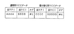
図33に示されるDS3−SMDSインタフェース1は、4.2 において説明したように、伝送路2から入力されたL2−PDUのヘッダに対してHCS(HEC)チェックを実行した後、53オクテットのL2−PDRU からATM スイッチ5内で処理可能な54オクテットのATM セルへの変換を行う。この場合、図35に示されるように、L2−PDUのヘッダ部に含まれるセグメントタイプ(SEGT)とメッセージ識別子(MID) 、並びに、L2−PDUのペイロード部に含まれるセグメンテーションユニット(SEG.UNIT)、ペイロードレングス(PLEN)、及びペイロードCRC(PCRC) が、ATM セルのペイロード部(ATM CELL PAYLOAD)に格納される。また、L2−PDUのヘッダ部内のネットワークコントロールインフォメーションフィールド(NCI) に含まれる全てのビット (20ビット) が“1”であるVCI は、DS3−SMDSインタフェースとSIFSH Commonとのインタフェースとして規定される値:VPI=3F,VCI=03FFに変換されて、そのVPI/VCI がATM セルのヘッダ部に付加される。
以上説明したようにして、図33のDS3−SMDSインタフェースは、伝送路1上のDS3 フォーマットと、SIFSH 6内の共通部(COM) で処理可能なATM セルフォーマットとの間で、相互に変換を行う。この場合、SMDSサービスにおけるユーザデータを伝送するL3−PDU(L3 プロトコルデータユニット) は、上記両フォーマットを用いて伝送されるL2−PDUのペイロード部内のセグメンテーションユニットに格納されて伝送される。
即ち、図42に示されるように、DS3 伝送路を使って通信を行う送信側ユーザ端末においては、まず、通信データ (ユーザデータ) が、SMDSサービスにおいて規定されるL3−PDUのペイロード部に格納される。次に、送信側ユーザ端末においては、L3−PDUが、それぞれ44オクテットからなる1つ又は複数のセグメントに分割される。次に、その1つ又は複数のセグメントのそれぞれが各ペイロード部内のセグメンテーションユニットに格納された1つ又は複数のL2−PDUが組み立てられる。この場合、1つのL3−PDUから生成される1つ又は複数のL2−PDUには、同じ値を有するMID(Message Identifier, or Multiplexing Identification) と呼ばれる識別子 (図35、図38参照) が付与される。これは、SMDSサービスを提供するための後述するSBMESH(Subscriber Message Handler Shelf,図8参照) が、L3−PDUを認識することはせずにL2−PDUのヘッダ部のみをリアルタイムで認識してSMDSのデータを処理するために、必要な情報である。なお、ユーザは、1つのSNI(Subscriber Network Interface) 上において、同時に16種類のMID値を使用することができる。即ち、ユーザは、1つのSNI 上で同時に16種類のSMDSメッセージを通信することができる。続いて、送信側ユーザ端末においては、L2−PDUからPLCPフレームが組み立てられ、更にDS3 フレームのサブフレームが組み立てられ、最後にDS3 フレームのマルチフレームが組み立てられる (図35参照) 。このようにして送信側ユーザ端末で組み立てられたDS3 フレームが、DS3 伝送路に送出される。そして、DS3−SMDSインタフェースは、前述のようにして、DS3 フレームからPLCPフレームを抽出し、PLCPフレームからL2−PDUを抽出し、L2−PDUをATM セルに変換して、SIFSH Commonに送出する。このように、DS3−SMDSインタフェースは、SMDSサービスにおけるL3−PDUは一切認識する必要はない。
SIFSH Commonは、DS3−SMDSインタフェースから入力されたペイロード部にSMDSサービスのL2−PDUを含むATM セルのヘッダ部に付加されているVPI/VCI の値を、DS3−SMDSインタフェースで付加された値:VPI=3F,VCI=03FFから、SIFSH CommonとSBMESH (図8参照) の間に張られるPVC(Permanent Virtual Circuit:相手固定接続) を特定すると同時に、そのATM セルを送出したDS3−SMDSインタフェースが終端するDS3 伝送路であるSNI を特定するVPI/VCI の値に、付け替える。従って、SIFSH CommonとSBMESHの間に張られるPVC には、そのSIFSH Commonに接続されSMDSサービスに使用されるDS3−SMDSインタフェースを始めとする個別部が終端するSNI の数に対応する数のVPI/VCI の値が割り当てられることになる。また、SIFSH Commonは、そのATM セルの先頭に、そのATM セルがATM スイッチ内で自律的にスイッチングされてSBMESHに転送されるようにするための、タグを付加する。
ATM スイッチ(ASSWSH)に接続されSMDSサービスを提供する後述するSBMESH (図8参照) 等は、ATM スイッチから入力されるのATM セルのうち、ヘッダ部にSMDSサービスに使用されるPVC に対応する特定のVPI/VCI 値が付加されているATM セルを受信し、図42に示されるように、そのATM セルのペイロード部に格納されているL2−PDUを処理する。なお、ATM セルは、レイヤ2(L2)内のATM レイヤのプロトコル階層を有し、L2−PDUはレイヤ2(L2)のAAL(ATM Adaptation Layer) 内のSAR(Segmentation and Reassembly Sublayer) のプロトコル階層を有する。この場合、パート5等において後述するように、SBMESH等は、レイヤ3(L3)のプロトコル階層を有し、SMDSサービスにおけるユーザ情報(User data) が実際に格納されて伝送されるL3−PDU (図42) を認識することはせずに、ATM セルのヘッダ部及びL2−PDUのヘッダ部のみをリアルタイムで認識してSMDSのデータを処理する。具体的には、SBMESHは、ATM セルのヘッダ部に付与されているVPI/VCI の値によって判別されるSNI が同じで、かつL2−PDUのヘッダ部に付与されているMID の値が同じL2−PDUを、同じL3−PDUを転送するデータとして処理する。この結果、ATM 方式が有するリアルタイム性という特徴を損なわずにコネクションレスサービスであるSMDS サービスを提供することが可能となる。
一方、DS3 伝送路を使って通信を行う受信側ユーザ端末では、まず、DS3 伝送路から受信されたDS3 フレームからPLCPフレームが抽出され、PLCPフレームからL2−PDUが抽出される。そして、L2−PDUのペイロード部内のセグメンテーションユニットの内容が抽出され、L2−PDUのヘッダ部に付加されているMID に基づいてL3−PDUが組み立てられる。最後に、そのL3−PDUのペイロード部から通信データ (ユーザデータ) が抽出される。
6.DS3 アンビリカルリンクフォーマット
図34に示されるように、DS3 伝送路4にBRLC(Broadband Remote Line Concentrator:広帯域遠隔回線集線装置) が接続される場合には、DS3−SMDSインタフェース3は、アンビリカルリンクを実現する。
この場合、伝送路4上のデータは、図43に示される53オクテットからなるデータフォーマットにより伝送される。即ち、伝送路4上のデータは、通常のATM セルとして伝送される。
図43に示されるように、ヘッダ部(HEADER)には、VPI(Virtual Pass Identifier)、VCI(Virtual Channel Identifier) 、PTI(Payload Type)、CLP(Cell Loss Priority)、及びHEC(Header Error Check) からなる5オクテットのデータによって構成される。
HEC(Header Error Check) 部は、上記ヘッダ部に対する生成多項式(G(x)= X8 +X2 +X+1) を用いた計算によって得られる値である。この値を用いることによって、ヘッダ部のエラーチェックが行われる。
このエラーチェックの結果が正常である場合は、図44に示されるように、VIP とVCI の値が全て“0”であるか否かが判定されることにより、処理対象のATM セルが無効セル(UNASSIGNED CELL) であるか有効セル(ASSIDNED CELL) であるかが判定される。
また、エラーチェックの結果、1ビット誤りが検出された場合にはその誤りが訂正され、2ビット誤り以上の誤りが検出された場合にはその誤りは訂正されずにその誤りの検出のみが行われる。
DS3−SMDSインタフェース3は、伝送路4から受信したATM セルについて、そのヘッダ部の1オクテットのHEC を除去すると共に2オクテットのタグを付加することにより、伝送路4上で53オクテットからなるATM セルをATM スイッチ内で処理可能な54オクテットからなるATM セルに変換する。
この場合に、SMDSサービスにおけるL2−PDUは、図43に示されるATM セルのペイロード部(PAYLOAD)に格納される。
7.ハードウエアコンフィギュレーション
7.1 概略説明
ここまで説明してきたDS3−SMDS機能は、図33に示されるDS3−SMDSインタフェース1、3と、図8に示されるSBMESH(Subscriber Message Handler Shelf)及びGWMESH(GatewayMessage Handler Shelf)によって実現される。
これらの各部分の機能の分担は、以下の通りである。
1.DS3−SMDSインタフェース部
a.DS3 レイヤ終端機能
b.DS3 PLCP レイヤ終端機能
b.L2−PDUヘッダ終端機能
2.SBMESH/GWMESH インタフェース部
a.L2−PDUペイロード終端機能
b.L3−PDU終端機能
DS3−SMDSインタフェース部に搭載される機能を更に細分化して示すと、以下の通りになる。
a.DS3 レイヤ終端機能
b.DS3 PLCPレイヤ終端機能
c.受信L2−PDUヘッダチェック機能(HCS)
d.L2−PDUヘッダパターン生成機能
e.DQDB(Distributed Queue Dual Bus)シーケンス機能(REQビット処理機能)
f.DS3 レイヤパフォーマンスモニタ機能
g.PLCPレイヤパフォーマンスモニタ機能
h.受信L2−PDUデータ変換機能 (45Mbps→156Mbps)
i.送信L2−PDUデータビットレート変換機能(156Mbps→45Mbps)
j.MSD/MSCN情報のLAP 終端機能
k.SIFSH Commonに対するインタフェース機能 (53オクテット 8ビットパラレル−54オクテット 16ビットパラレル)
l.DS3−SMDS L2−PDU セル及びLAP セルのマルチプレクス/デマルチプレクス機能
m.特定VPI/VCI セルのループバック機能
n.MSCNデータのマルチプレクス機能
o.MSD データドロッパ機能
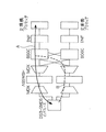
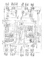
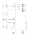
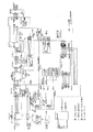
図45に、DS3−SMDSインタフェースの機能構成ブロック図を示す。
7.2 DS3 レイヤ終端機能
DS3−SMDSインタフェース部に搭載される機能の1つであるDS3 レイヤ終端機能では、2.1.2において図35を用いて前述した、DS3 フレームフォーマットの終端処理が実行される。
より具体的には、以下の処理が実行される。
A.受信側
a.PCM ライン符号 (B3ZS符号) に対する違反監視及びエラーカウント
b.フレーミングビット(FO/F1/MO/M1 :図36参照) に対する同期確立及 びエラーカウント
c. Pビット (パリティビット :図36参照) の確認及びそれに対するエ ラーカウント
d. AISパターン (図36参照) の確認
e.イエローアラームビット(Xビット :図36参照) の確認
B.送信側
a.フレーミングビット(FO/F1/MO/M1 :図36参照) の生成
b. Pビット (パリティビット :図36参照) の生成
c. AISパターン (図36参照) の生成 (ループバック指定時)
d.レッドCGA アラーム時におけるイエローアラームビット(Xビット :図39参照) の設定
e.PCM ライン符号 (B3ZS符号) の変換
7.2.1 回線障害処理
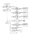
DS3−SMDSインタフェースは、回線障害を監視しており、障害発生時には障害を交換機システムへ通知する。この障害通知は、障害の復旧にともない自動的に正常通知に復旧する。障害監視中に複数の障害が検出された場合は、その根本原因となる障害に対してのみ監視処理が実行され、その障害に起因する他の障害に対しては監視処理は実行されない。
図46に、DS3 レイヤにおけるアラームのシーケンスを示す。まず、図46(a) において、伝送路上で障害が発生すると(1.)、DS3−SMDSインタフェースAは、レッドCGA(Carrier Group Alarm)を宣言し(2.)、続いてイエローアラームを送信する(3.)。この結果、DS3−SMDSインタフェースBは、イエローCFA(Carrier Failure Alarm)を宣言する(4.)。次に、図46(b) において、DS3−SMDSインタフェースAは、折り返し試験状態になると(1.)、AIS(Alarm Indication Signal)を送信し(2.)、この結果、DS3−SMDSインタフェースBはAIS 受信宣言を行う。
図47は、DS3 レイヤにおけるアラームの優先度を示す。例えば、LOS(LossOf Signal)が検出されると、AIS(Alarm Indication Signal)、OOF(Out Of Frame) 、YEL(Yellow Signal)、POOF(PLCP Out Of Frame) 、及びPYEL(PLCP Yellow Signal)の各アラームがマスクされる。
7.2.2 各種アラームの検出・復旧条件
図48に、各種アラームの検出・復旧条件を示す。また、図49に、アラームが宣言されるタイミングを示す。
7.3 DS3 PLCPレイヤ終端機能
DS3−SMDSインタフェース部に搭載される機能の1つであるDS3 PLCPレイヤ終端機能では、3.1において図37を用いて前述した、DS3 PLCPフレームフォーマットの終端処理が実行される。
より具体的には、以下の処理が実行される。
A.受信側
a.フレーミングビット(A1/A2 :図37参照)に対する同期確立及びエラーカウント
b.PLCP BIP−8(B1:図37参照) の確認及びそれに対するエラーカウント
c.PLCPパスステータス(G1:図37参照) の確認及びそれに対するエラーカウント
B.送信側
a.フレーミングビット(A1/A2 :図37参照) の生成
b.PLCP BIP−8(B1:図37参照) の生成
c.PLCPパスステータス(G1:図37参照) の生成
d.サイクル/スタッフカウンタ(C1:図37参照) の生成
e.SIP レベル1コントロールインフォメーション(M1/M2 :図37参照) の生成
7.3.1 PLCP障害処理
DS3−SMDSインタフェースは、PLCP障害を監視しており、障害発生時には障害を交換機システムへ通知する。この障害通知は、障害の復旧にともない自動的に正常通知に復旧する。障害監視中に複数の障害が検出された場合は、その根本原因となる障害に対してのみ監視処理が実行され、その障害に起因する他の障害については監視処理は実行されない。
図50に、DS3 PLCPレイヤにおけるアラームのシーケンスを示す。図50において、まず、DS3−SMDSインタフェースBにおいてPLCPフレームの送信障害が発生すると(1.)、DS3−SMDSインタフェースAはPLCPフレームの同期外れを検出した後にイエローシグナルを送信する。この結果、DS3−SMDSインタフェースBはイエローシグナルの受信宣言を行う。
7.3.2 各種アラームの検出・復旧条件
図51に、各種アラームの検出・復旧条件を示す。また、図52に、アラームが宣言されるタイミングを示す。
7.4 L2−PDUヘッダチェック機能(HCS)
前述の図33に示されるように、DS3−SMDSインタフェース1がSMDSサービスを提供するためのDS3 伝送路2上のDS3 レイヤーを終端する場合、DS3−SMDSインタフェース1は、DS3 伝送路2から入力されるDS3 フレームのインフォメーションペイロード部に収容されているPLCPレイヤーのフレームを取り出す。そして、DS3−SMDSインタフェース1は、取り出したPLCPレイヤーのフレームからL2プロトコルデータユニット(L2−PDU)を抜き出す (図35参照) 。更に、DS3−SMDSインタフェース1は、L2−PDUのヘッダ内のアクセスコントロールフィールド(ACF、図38、図39、図35参照) に含まれるBUSYビットを参照することによって、L2−PDUが有効セルの可能性があるか無効セルの可能性があるかを判定する。L2−PDUが有効セルの可能性がある場合、DS3−SMDSインタフェース1は、L2−PDUのヘッダ内のネットワークコントロールインフォメーションフィールド(NCI、図38、図35参照) の値が、図40に示されるように、11111111 11111111 11110000 00100010 であるかオール“0”であるかを判定する。NCI の値が11111111 11111111 11110000 00100010 である場合には、DS3−SMDSインタフェース1は、対象となっているL2−PDUを真に有効なセルとして処理する。逆に、NCI の値がオール“0”である場合には、DS3−SMDSインタフェース1は、HCS エラーのカウント値をインクリメントし、プロトコルモニタ処理を実行する。
一方、前述の図34に示されるように、DS3 伝送路4にBRLCが接続され、DS3−SMDSインタフェース3がアンビリカルリンクを実現している場合には、DS3−SMDSインタフェース3は、ATM ヘッダ部のHEC(図43参照) を計算し、その計算の結果ATM ヘッダ部でエラーが発生していないと判定した場合には、更に、対象となっているATM セルが空セルであるか否かをチェックした後に、対象となっているATM セルが有効なセルであるか否かを決定する。また、DS3−SMDSインタフェース3は、上記HEC 計算の結果ATM ヘッダ部でエラーが発生していると判定した場合には、HEC エラーのカウント値をインクリメントし、プロトコルモニタ処理を実行する。
7.5 L2−PDUヘッダパターン生成機能
前述の図33に示されるように、DS3−SMDSインタフェース1がSMDSサービスを提供するためのDS3 伝送路2上のDS3 レイヤーを終端する場合、DS3−SMDSインタフェース1は、図33のATM スイッチ(ASSWSH)5の側から転送されてくるATM セルが有効セルである場合、図35に示されるようにそのATM セルのペイロード部に含まれている情報の前部に、11111111 11111111 11110000 00100010 の値を有するネットワークコントロールインフォメーションフィールド(NCI) を付加し (図40参照) 、更にその前部にアクセスコントロールフィールド(ACF) を付加することによりL2−PDUを構築する。また、DS3−SMDSインタフェース1は、図33のATM スイッチ(ASSWSH)5の側から転送されてくるATM セルが無効セルである場合は、図35に示されるようにそのATM セルのペイロード部に含まれている情報の前部に、オール“0”であるNCI を付加し (図40参照) 、更にその前部にアクセスコントロールフィールド(ACF) を付加することによりL2−PDUを構築する。このように、ATM セルがL2−PDUに変換される際には、ATM セルのヘッダ情報(VPI/VCI等) は破棄される。その後、図35に示されるように、上述のようにして構築されたL2−PDUに基づいてPLCPレイヤーのフレームが構築され、更にこのPLCPレイヤーのフレームに基づいてDS3 フレームが構築され、そのDS3 フレームが図33のDS3 伝送路2に送出される。
一方、前述の図34に示されるように、DS3 伝送路4にBRLCが接続され、DS3−SMDSインタフェース3がアンビリカルリンクを実現している場合には、DS3−SMDSインタフェース3は、ATM スイッチ(ASSWSH)の側から転送されてくるATM セルに対して、そのヘッダ部の付替えは行わずに、そのヘッダ部に対するHEC 計算のみを行いその結果得られるHEC(図43参照) をそのヘッダ部に付加した後に、そのATM セルを図34の伝送路4に送出する。
7.6 DQDB(Distributed Queue Dual Bus)シーケンス機能
前述の図33に示されるように、DS3−SMDSインタフェース1がSMDSサービスを提供するためのDS3 伝送路2上のDS3 レイヤーを終端する場合において、そのDS3 伝送路2に接続されているユーザ端末であるCPE(Customer Premise Equipment) が例えばLAN に接続されるマルチCPE である場合に、次のような制御が行われる。即ち、CPE が空セルを捕捉できなかった場合に、そのCPE は、伝送路上のL2−PDUのヘッダ内のアクセスコントロールフィールド(ACF、図38、図35参照) に含まれるREQ0−REQ2 のビット (図39参照) をオンすることにより、空セルを要求する。そして、図33に示されるDS3−SMDSインタフェース1は、CPE から上記要求ビットを受信した場合に、空セルを送出する。
7.7 DS3 レイヤ/PLCPレイヤパフォーマンスモニタ機能
DS3−SMDSインタフェースは、回線のパフォーマンスをモニタしており、単位時間(15分及び1日) 間隔で、各種パフォーマンスパラメータの積算及びその結果得られる積算値に対する閾値アラームを交換機システムに通知する。
交換機システムは、閾値アラームの通知を受けても、そのアラームに対応する回線を閉塞せずにそのアラームを単なる警報として扱い、その事実を以後の保守計画に反映させる。
パフォーマンスパラメータは、DS3 レイヤに関するものとPLCPレイヤに関するものに大きく分類される。DS3 レイヤに関しては更に、回線に関する情報とパスに関する情報とに分類することができる。
DS3 レイヤにおける回線に関する情報としては、以下の3種類のパラメータについての観測が行われる。
1.LCV : Line Code Violation
2.LES : Line Errorred Second
3.LSES: Line Severly Errorred Second
DS3 レイヤにおけるパスに関する情報としては、以下の6種類のパラメータについての測定が行われる。
4.CV : P−bit Parity Code Violation
5.ES : Errorred Second
6.SES : Severly Errorred Second
7.SEFS: Severly Errorred Second
8.UAS : Unavailable Second
9.AISS: Alarm Indication Signal Second
PLCPレイヤに関する情報としては、以下の5種類のパラメータについての測定が行われる。
10.PLCP CV : PLCP Code Violation
11.PLCP ES : PLCP Errorred Second
12.PLCP SES: PLCP Severly Errorred Second
13.PLCP OOF: PLCP Out Of Frame
14.PLCP UAS: PLCP Unavailable Second
DS3−SMDSインタフェースは、15分毎に得られる過去1回分の測定結果を保持する。この測定結果は、交換機システムによって15分時間毎に読み出される。交換機システムは、15分毎に得られるその測定結果を、1日あたり過去32回分(8時間分) 保持し、更に過去7日分保持する。
また、PLCPフレームフォーマット内のG1ビット (図37参照) を用いて伝送されるFar End Block Error(FEBE) を使用したFAR END のパフォーマンスモニタ機能も提供される。この機能における閾値は、デフォルト値であって、ユーザが自由に設定できる。
7.7.1 DS3 レイヤ
図53に、DS3 レイヤに関するパフォーマンスパラメータの種類と、各パラメータの積算値のカウントアップ条件を示す。
7.7.2 DS3−PLCPレイヤ
図54に、DS3−PLCPレイヤに関するパフォーマンスパラメータの種類と、各パラメータの積算値のカウントアップ条件、各パラメータの積算値に対するアラート閾値を示す。
7.8 受信L2−PDUデータ変換機能 (45Mbps→156Mbps)
7.4で前述したL2−PDUヘッダチェック処理の結果、L2−PDUヘッダでエラーが発生しておらず、かつそのL2−PDUが有効セルであると判定された場合には、そのL2−PDUを変換して得られるATM セルが、SIFSH Commonを介してATM スイッチ(ASSWSH)に送出される (図8参照) 。この場合に、有効セルが連続的にユーザ側から送出されてくると、ATM スイッチで処理されるデータのバースト性が高くなり、ATM スイッチ内において輻輳が発生し、ATM スイッチ内においてセル紛失が発生する可能性がある。そのため、DS3−SMDSインタフェースは、バッファを用いることによって、45Mbpsのビットレートを有するDS3 伝送路から受信したL2−PDUをSIFSH Commonが終端する156Mbps のビットレートを有する交換機内ハイウエイに多重する場合に、そのハイウエイに多重される有効セルと無効セルの割合が3:1 となるようなシェーピングを行う。
7.9 送信L2−PDUデータビットレート変換機能(156Mbps→45Mbps)
SIFSH Commonより送出されるL2−PDUのビットレートは156Mbps である。このため、DS3−SMDSインタフェースは、156Mbps のビットレートを有するデータを、DS3 レイヤのビットレートである45Mbpsのビットレートに変換する。
7.10 SIFSH Commonに対するインタフェース機能
DS3−SMDS L2−PDU のセル長は53オクテットであり、SIFSH Common(SIFSH COM、図33参照) が処理するATM セルのセル長は54オクテットである。そのため、DS3−SMDSインタフェースとSIFSH Commonの間のインタフェースは、データ長の変換機能を有する必要がある。
DS3−SMDSインタフェースからSIFSH CommonへL2−PDUが転送される場合、DS3−SMDSインタフェースは、伝送路から入力されたL2−PDUのヘッダに対してHCS(HEC)チェックを実行した後、53オクテットのL2−PDUからATM スイッチ5内で処理可能な54オクテットのATM セルへの変換を行う。この場合に、図35に示されるように、L2−PDUのヘッダ部に含まれるセグメントタイプ(SEGT)とメッセージ識別子(MID) 、並びに、L2−PDUのペイロード部に含まれるセグメンテーションユニット(SEG.UNIT)、ペイロードレングス(PLEN)、及びペイロードCRC(PCRC) が、ATM セルのペイロード部(ATM CELL PAYLOAD)に格納される。また、L2−PDUのヘッダ部内のネットワークコントロールインフォメーションフィールド(NCI) に含まれる全てのビットが“1”であるVCI は、DS3 インタフェースとSIFSH Commonとのインタフェースとして規定される値:VPI=3F,VCI=03FFに変換され、そのVPI/VCI がATM セルのヘッダ部に付加される。また、ATM セルのヘッダ部には、それが各種多重化部及びATM スイッチ内で自律的にスイッチングされるための2オクテットからなるタグが付加される。
SIFSH CommonからDS3−SMDSインタフェースへATM セルが転送される場合は、DS3−SMDSインタフェースは、ATM セルにおける先頭のタグをチェックしその結果自身が出力すべきセルである場合にそのタグを削除する。その後、DS3−SMDSインタフェースは、DS3−SMDSインタフェースからSIFSH CommonへL2−PDUが転送される場合と全く逆の操作を行うことにより、54オクテットからなるATM セルを53オクテットからなるL2−PDUに変換する。
図55は、以上の変換処理をまとめて示した図である。アクセスコントロールフィールド(ACF、図35、図38参照)についても、図55に示されるように変換される。また、共にオール“0”の値を有するペイロードタイプ(PT)及びセグメントプライオリティ(SP) (共に図40参照) は、そのまま転送される。
DS3−SMDSインタフェースがアンビリカルリンクを実現する場合には、DS3−SMDSインタフェースは、伝送路から受信したATM セルについて、そのヘッダ部の1オクテットのHEC を除去すると共に2オクテットのタグを付加することにより、伝送路4上で53オクテットからなるATM セルをATM スイッチ内で処理可能な54オクテットからなるATM セルに変換し、それをSIFSH Commonに送出する。即ち、VPI/VCI の変換は行われない。SIFSH CommonからDS3−SMDSインタフェースにATM セルが転送される場合には、上記の場合と全く逆の操作が行われる。
7.11 MSD/MSCN情報のLAP 終端機能
交換機システムからDS3−SMDSインタフェースへ転送される制御情報(MSD情報) と、DS3−SMDSインタフェースから交換機システムへ転送される、パフォーマンスモニタ閾値交差アラート、パフォーマンスモニタカウンタ値等のDS3 レイヤ/PLCPレイヤ障害情報(MSCN)は、LAPD(Link Access Protocol)を用いて伝送される。そして、このLAPDは、タイプ3又は4のAAL(ATM Adaptation Layer) プロトコルタイプを用いてATM セルにマッピングされる。この結果、上記各情報は、ATM セルとして、ATM スイッチ(ASSWSH)を通って、DS3−SMDSインタフェースと交換機システム側のBSGCSH(Broadband Signaling Group Controller Shelf 、図8参照) との間を伝送されることになる。
なお、DS3−SMDSインタフェースのハードウエア障害(Parity Error 等の障害) は、SIFSH CommonがLAPDを用いて交換機システムに通知する。交換機内を転送されるデータがL2 PDUデータであるかLAPDデータであるかの区別は、ATM セルのヘッダ部のタグ領域内の特定のビットの値により区別される。図56に、交換機内を転送されるATM セルのフォーマットを示す。交換機内を転送されるデータがL2 PDUデータであるかLAPDデータであるかの区別は、ATM セルの先頭に付加される2オクテットからなるタグ領域内のSIG ビットの値により区別される。
このように、DS3−SMDSインタフェース及びSIFSH Commonなどを交換機システムのシステムバスに直接接続する必要がなくなるため、システムバスにかかる負荷を軽減させることができる。
7.12 DS3−SMDS L2−PDU セル及びLAP セルのマルチプレクス機能
DS3−SMDSインタフェースは、SIFSH Commonの方向へ転送するATM セルにおいて、L2 PDUデータに対してMSCN LAPD セルをマルチプレクスする。MSCN LAPD セルのマルチプレクスタイミングとして、交換機システム側よりMSD LAPDセルを用いてパフォーマンスモニタ情報等の要求があった時に、L2 PDUデータに対してMSCN
LAPD セルがマルチプレクスされる。
7.13 DS3−SMDS L2−PDU セル及びLAP セルのデマルチプレクス機能
SIFSH CommonからDS3−SMDSインタフェースへ転送されてくるATM セルにおいては、L2 PDUデータに対してMSD LAPDセルがマルチプレクスされている。そのため、DS3−SMDSインタフェースは、MSD LAPD情報を処理するために、MSD LAPDセルをデマルチプレクスする必要性がある。デマルチプレクス処理は、図56に示したATM セルのタグ領域内のSIG ビットの値を判定して行われる。
7.14 特定VPI/VCI セルのループバック機能
7.14.1 “0”ビットが付加されたセルのループバック機能
DS3−SMDSインタフェースには、メンテナンス機能として、図56に示されるATM セルのタグ領域の先頭に“0”ビットが付加された特定のセルをループバックする機能が搭載されている。
7.14.2 特定VPI/VCI が付加されたセルのループバック機能
DS3−SMDSインタフェースには、メンテナンス機能として、簡易LAP を用いて通知された特定VPI/VCI が付加されたセルのループバック機能が搭載される。このループバックは、簡易LAP フォーマットを用いてVPI/VCI 値が通知された後、E−MSD 情報によって起動される。但し、このループバック機能と、7.14.1に示した“0”ビットが付加されたセルのループバック機能は、ハードウエアの構成上、同時には起動されない。
7.15 MSCNデータマルチプレクス機能
DS3−SMDSインタフェースからMSCN LAPD セルを用いて通知できないDS3−SMDSインタフェースのハードウエア障害(Parity Error 等の障害) 情報は、SIFSH CommonがLAPDセルを用いて交換機システムに通知する。そのため、DS3−SMDSインタフェースからの障害情報は、1Mbps のシリアルデータとして送出される。
7.16 MSD データドロッパ機能
SIFSH に搭載されるラインインタフェースに転送される共通的な情報は、SIFSH Commonで終端される。そのために、DS3−SMDSインタフェースへ転送される情報は、7.15で説明した場合と同様に、1Mbps のシリアルデータとして転送されてくる。DS3−SMDSインタフェースは、このようにして転送されてくるMSD データを処理する。
8.MSD(Maintenance Signal Driver)インタフェース
8.1 MSD情報
交換機システムのソフトウエアからDS3−SMDSインタフェースへ通知される情報のうち以下に示すものは、局内制御通信を用いてBSGCSH (図8参照) 経由で、一旦、交換機システムのソフトウエアからSIFSH Commonに転送される。そして、SIFSH Commonが、これらの情報を、ソフトウエア処理によってDS3−SMDSインタフェースへ通知する。このような種類の情報は、E−MSDと称される。
1.各種リセット信号
2.DS3−SMDSインタフェース状態制御情報
3.ソフトウエア障害検出回路の疑似障害設定情報
4.時計情報等の、SIFSH CommonよりDS3−SMDSインタフェースをはじめとする各個別部へ同時に通知される情報
E−MSD 情報は2重化されたSIFSH Commonの両方の系で受信されるが、DS3−SMDSインタフェースは、アクティブなSIFSH Commonから転送されてきたE−MSD 情報を取り込む。ハードウエアの制限により、E−MSD 情報は、ビットスタック(stuck) 以外を検出する手段を持たない。このため、DS3−SMDSインタフェースは、SIFSH Commonの系の切替え時のクロック/フレームパルスの乱れに対処するため、受信したE−MSD 情報に対して保護処理を実行する。即ち、DS3−SMDSインタフェースは、SIFSH Commonから連続して2フレーム分の同じ情報を受信した場合に初めて、その情報を有効なデータとして処理する。
8.1.1 E−MSD ハードウエアインタフェース
E−MSD 情報の、SIFSH CommonとDS3−SMDSインタフェース間のインタフェースとは、クロック(1.215MHz)、FP (フレームパルス) 、データの3つの要素について規定される。E−MSD のデータ長は、256 ビットである。図57に、E−MSD 信号のタイミングチャートを示す。
8.1.2 DS3−SMDSインタフェースにおけるE−MSD 収容表
図58に、DS3−SMDSインタフェースとSIFSH Common間を転送されるE−MSD 情報の収容状態を表した表を示す。この表において、縦方向はバイト位置を示し、横方向はそれぞれのバイト位置内のビット位置を示す。SIFSH Commonから転送されてくるE−MSD データは、DS3−SMDSインタフェースで、第000 バイト第D0ビット→第255 バイト第D7ビットの順序で、シリアルに受信される。このフォーマットにおいて第000 バイト領域は、SIFSH Commonで生成されるため、第001 バイトが設定されるデータの実質的な先頭になる。
DS3−SMDSインタフェースは、ハードウエアリセット信号を含む各種リセット信号を自動的に解除しないため、それらのリセット信号は、それらが設定された後は必ず解除される必要がある。
図59に、E−MSD 情報の各ビットの内容を示す。
8.2 E−MSD詳細説明
8.2.1 ハードウエアリセット
DS3−SMDSインタフェースにおいては、ハードウエア障害発生時のリセットタイミングとして、以下に示す2種類のリセットポイントが規定される。
1.SDFRST (ハードウエア障害リセット)
2.μPRST (マイクロプロセッサリセット)
これらのリセットは、ハードウエアによって自動的にそのリセットタイミングのエッジが生成されないため、セット時に“1”、リセット時に“0”が設定される必要がある。
8.2.2 ループバック
DS3−SMDSインタフェースにおいては、メンテナンスのために、以下に示す3種類の全セルに対するループバックの起動ポイントと、セル by セルのループバックの起動ポイントが規定される。
1.LOOP−1 (DS3−SMDSインタフェース入力部 (ASSW側) での全セルのループバック指示)
2.LOOP−2 (DS3−SMDSインタフェース出力部 (回線側) での全セルのループバック指示)
3.LOOP−3 (入力DS3 伝送路からの全セルの出力DS3 伝送路へのラインループバ
ック指示) 4.O−LOOP (“0”ビットが付加されたセルのループバック指示)
5.V−LOOP (特定VPI/VCI が付加されたセルのループバック指示)
8.2.3 疑似障害ポイント
DS3−SMDSインタフェースが受信するE−MSD には、インタフェース内に設けられているハードウエアチェッカに対して指定される疑似障害ポイントが収容される。疑似障害ポイントとしては、以下に示す5種類が規定される。
1.PF−CK(クロック断チェッカに対する疑似障害ポイント)
2.PF−CK(セルフレームパルス断チェッカに対する疑似障害ポイント)
3.PF−PTY (データパリティチェッカに対する疑似障害ポイント)
4.PF−WDT (ウオッチドッグタイマチェッカに対する疑似障害ポイント)
5.PTYRST (データパリティエラーリセット)
これらのポイントに関しては、8.2.1で説明したリセットの場合と同様に、セット時に“1”、リセット時に“0”が設定される必要がある。但し、パリティエラーは、保持タイプの情報であるため、PTYRSTによってリセットされる必要がある。また、この疑似障害については、DS3−SMDSインタフェース内のPCB(Printed Circuit Board 、プリント回路板) 内に設けられている全てのチェッカを起動させるために、疑似障害ポイントの全てがオンされる。
8.2.4 AIS 送出ポイント
DS3−SMDSインタフェースは、対向装置に対して障害閉塞等の閉塞を通知するために、ソフトウエア制御によってDS3 伝送路上に上にAIS パターン(AISSND)を送出する機能を有する。
9.MSCN(Maintenance SCaNer)インタフェース
DS3−SMDSインタフェースより交換機システム側のソフトウエアへ通知される情報のうち以下に示すものは、ハードウエアにより一旦SIFSH Commonへ転送される。そして、SIFSH Commonが、局内制御通信を用いてBSGCSH (図8参照) 経由で、交換機システムのソフトウエアに通知する。このような種類のMSCN情報は、特にE−MSCN(Extended Maintenance Scanner)情報と称される。
1.DS3−SMDSインタフェースとSIFSH Commonの間の信号線の障害情報 (パリティクロックロス、セルフレームロス)の代表ポイント及び詳細情報
2.DS3−SMDSインタフェース自身のハードウエア障害情報の代表ポイント
3.DS3−SMDSインタフェースとBSGCSH間の局内制御通信が不可能となるような障害に関する代表ポイント及び詳細内容
4.DS3 レイヤ/PLCPレイヤでのアラーム監視に基く回線障害の代表ポイント
5.DS3−SMDSインタフェースにおけるバッファ輻輳の発生時の品質制御情報の代表ポイント
6.MSD のエコーバック情報
7.その他、DS3−SMDSインタフェースとSIFSH Commonの間の保守・制御情報
E−MSCN情報は、DS3−SMDSインタフェースから2重化されたSIFSH Commonの両方の系に、同じ内容のものが送出される。E−MSCNを送出するためのクロックとフレームパルスは、アクティブなSIFSH Commonより供給されたものが使用される。
SIFSH Commonは、DS3−SMDSインタフェースより受け取った有効なE−MSCN情報について、自身が保持しているE−MSCN情報の最新の内容と比較して変化のあったものを、局内制御通信を用いてBSGCSH (図8参照) 経由で、交換機システムのソフトウエアに通知する。SIFSH Commonは、DS3−SMDSインタフェースからのE−MSCN情報以外にも、自身に接続されている各個別部からのE−MSCN情報を、局内制御通信を用いてBSGCSH経由で、交換機システムのソフトウエアに定期的に通知する。
9.1.1 E−MSCNのハードウエアインタフェース
E−MSCNを送出するためのクロック及びフレームパルスは、アクティブなSIFSH Commonより供給されたものが使用される。
図60に、DS3−SMDSインタフェースとSIFSH Commonの間の信号線のタイミングチャートを示す。
9.1.2 E−MSCN の詳細
図61に、DS3−SMDSインタフェースとSIFSH Common間を転送されるE−MSCN情報の収容状態を表した表を示す。この表において、縦方向はバイト位置を示し、横方向はそれぞれのバイト位置内のビット位置を示す。DS3−SMDSインタフェースから転送されてくるE−MSCNデータは、SIFSH Commonで、第000 バイト第D0ビット→第255 バイト第D7ビットの順序で、シリアルに受信される。
図62及び図63に、E−MSCN情報の各ビットの内容を示す。
9.2 DS3−SMDSインタフェースでのE−MSCN処理
9.2.1 SIFSH Commonインタフェース障害
DS3−SMDSインタフェースは、SIFSH Commonインタフェース信号線の正常性監視を行っている。この正常性監視においては、SIFSH CommonからDS3−SMDSインタフェースの方向における、データパリティ (セルイネーブルも含む) 、クロック断、及びセルフレーム断がチェックされる。これらの監視によって障害の発生が検出された場合には、代表ポイントであるPEO(#0系) 又はPE1(#1系) がオンされる。この代表ポイントがオンされた時のSIFSH Commonインタフェース障害の詳細情報は、図61に示される第018 バイトの内容として確認することができる。
このSIFSH Commonインタフェース障害は、2重化されたSIFSH Commonのそれぞれの系のSIFSH Commonに互いに独立して接続されている信号線から入力されるFRST信号によってリセットすることができる。また、このリセット操作の後に、SIFSH Commonインタフェース障害が復旧していない場合には、上述した代表ポイント及び詳細情報ポイントが再びオンされる。
9.2.2 DS3−SMDSインタフェースハードウエア障害
DS3−SMDSインタフェースハードウエア障害としては、PCB(Printed Circuit Board 、プリント回路板) 内及びPCB 間のデータパリティ障害、クロック断、セルフレーム断がある。ここで、DS3−SMDSインタフェースとBSGCSH (図8参照) の間の局内制御通信を用いて通知可能なハードウエア障害が発生した場合は、E−MSCNに収容されている代表ポイントであるFERR−2がオンされる。障害の詳細情報の通知は、DS3−SMDSインタフェースとBSGCSH間の局内制御通信を用いて行われる。この詳細については、後述する10.で説明する。
このDS3−SMDSインタフェースハードウエア障害は、E−MSD に収容されているSDFRST情報及びSIFSH Commonから通知されるHRST情報によってリセットすることが可能である。また、このリセット操作後にDS3−SMDSインタフェースハードウエア障害が復旧していない場合には、FERR−2ポイントが再びオンされる。
9.2.3 局内制御通信が不可能となるDS3−SMDSインタフェースハードウエア障害
DS3−SMDSインタフェースとBSGCSH間の局内制御通信が不可能となるようなDS3−SMDSインタフェースハードウエア障害としては、DS3−SMDSインタフェースからSIFSH Commonの方向へのデータパリティ障害(UHDPT) 、マスター19M クロック断(UH19M) 、通信制御用EGCLAD障害(EGPTY) がある。これらの障害が発生した場合は、E−MSCNの代表ポイントであるFERR−1がオンされる。障害の詳細情報の通知は、局内制御通信が不可能であるため、E−MSCN上の第019 バイトに収容される。
この障害は、E−MSD に収容されているSDFRST情報及びSIFSH Commonから通知されるHRST情報によってリセットすることが可能である。また、このリセット操作後に上記障害が復旧していない場合は、FERR−1ポイントが再びオンされる。
9.2.4 マイクロプロセッサ障害
DS3−SMDSインタフェースには、DS3/PLCPレイヤパフォーマンスモニタ機能及び局内制御通信機能 (簡易LAPD) を処理するためにマイクロプロセッサが搭載されている。このマイクロプロセッサの障害及び暴走時には、E−MSCNのMPE ポイントがオンされる。
このマイクロプロセッサ障害は、E−MSD に収容されてるμPRST情報及びSIFSH Commonから通知されるHRST情報によってリセットすることが可能である。また、このリセット操作の後にマイクロプロセッサ障害が復旧していない場合には、MPE ポイントが再びオンされる。
9.2.5 タイマ障害
DS3−SMDSインタフェースは、SIFSH Commonに接続される専用の信号線を介して入力される15分及び1日のトリガーに基づいて、DS3/PLCPレイヤパフォーマンスモニタ等の処理を実行する。ところが、この専用線から入力されるべきトリガーが規定されているタイミングで入力しなくなった場合、即ち、前回の入力タイミングから15分+15秒以内に新たなトリガーが入力しなくなった場合には、パフォーマンスモニタ処理等の統計処理が実行できなくなる。このために、トリガーが規定通りに入力しなかった場合には、E−MSCNの代表ポイントであるTIMALMがオンされる。
このタイマ障害は、E−MSD に収容されているSDFRST情報及びSIFSH Commonから通知されるHRST情報によってリセットすることが可能である。また、このリセット操作後にタイマ障害が復旧していない場合には、TIMALMポイントが再びオンされる。なお、この障害ポイントはハードウエアモニタに基づいて収容されるため、特別なソフトウエア処理は実行するする必要性はない。
9.2.6 DS3 レイヤアラーム
DS3−SMDSインタフェースは、DS3/PLCPレイヤのキャリアグループアラーム(CGA) を監視している。このCGA アラームについては、複数のアラームがオンされる可能性がある。このため、CGA アラームは、共にE−MSCNの代表ポイントである、LIALM とアラーム状態の変化を示すLIFLGの2ビットによって通知される。
制御方法は次の通りである。即ち、LIALM ポイントは、DS3/PLCPレイヤアラームが検出されている時にオンされ、全てのアラームが復旧した時にオフされる。LIFLG ポイントは、DS3/PLCPレイヤアラームの状態が変化した時に、“0”から“1”又は“1”から“0”の交番形式で、その状態変化を通知する。
9.2.7 パフォーマンスモニタ閾値交差アラート
DS3−SMDSインタフェースは、DS3/PLCPレイヤ及びL2−PDUのネットワークコントロールインフォメーションフィールド内のHCS(Header Check Sequence) (図35、図38、図40参照) に関する閾値交差アラート(TCA) を監視している。このTCA は、15分及び1日の周期で監視対象値がそれに対して設定されている閾値を越えた時に通知される。従って、複数のTCA が同時にオンされる可能性がある。そのため、TCA は、共にE−MSCNの代表ポイントである、TCAALMとアラーム状態の変化を示すTCAFLGの2ビットによって通知される。
制御方法は次の通りである。即ち、TCAALMポイントは、DS3/PLCPレイヤのパフォーマンスモニタ値が閾値を越えた時にオンされ、15分及び1日を計時するタイマの状態が変化した時にオフされる。TCAFLGポイントは、DS3/PLCPレイヤのパフォーマンスモニタに関するTCA 状態が変化した時に、“0”から“1”又は“1”から“0”の交番形式で、その状態変化を通知する。但し、15分及び1日を計時するタイマの状態が変化した時は、TCAFLGポイントは前の状態を保持する。
9.2.8 DS3−SMDSインタフェースにおけるセル廃棄
DS3−SMDSインタフェースは、SIFSH Commonから転送されてくるATM セルの伝送レートを、SIFSH Commonにおける伝送レートである156Mbps からDS3 伝送路の伝送レートである45Mbpsセルに変換するために、その内部に112 セル分の容量を有するバッファを持っている。このバッファにおけるセルの輻輳の発生は、バッファ内のセル数がそのバッファに設定されているキュー(queue) 長の閾値を超えたか否かを判定することにより検出される。バッファは、バッファ内のセル数が上記閾値を超えた場合に、入力されるセルを廃棄する。そして、このような、バッファにおけるセルの輻輳状態は、共にE−MSCNの代表ポイントである、CLOSALとアラーム状態の変化を示すCLFLG の2ビットにより通知される。
制御方法は次の通りである。即ち、CLOSALポイントは、バッファにてセルの輻輳が検出されているときにオンされ、全てのセル廃棄状態が解除されたときにオフされる。また、CLFLG ポイントは、セル廃棄状態が変化した時に、“0”から“1”又は“1”から“0”の交番形式で、その状態変化を通知する。
9.2.9 診断結果通知
DS3−SMDSインタフェースは、ハードウエア機能の確認のために、自己診断機能を搭載している。この自己診断機能は、E−MSD に収容されているDS3 DEC ポイントをオンすることにいより、起動される。また、その診断結果は、共にE−MSCNに収容される代表ポイントであるTSTENDとTSTINDによって通知される。TSTENDポイントは自己診断が終了した時点でオンされる。TSTINDポイントは、診断結果が正常であるときに“1”、異常であるときに“0”にされる。また、診断結果が異常の場合には、E−MSCNに収容される第031 バイトを使って、異常が発生させられたフェーズナンバー及びテストナンバーを通知することができる。また、診断の終了後は、DS3−SMDSインタフェースは、リセット待ちの状態となるため、初期設定手順によって初期化される必要性がある。
10.DS3−SMDSインタフェース簡易LAP−D プロトコル
10.1 ソフトウエアインタフェース
図64に、DS3−SMDSインタフェースと交換機ソフトウエアの間のインタフェースの接続構成を示す。また、図65に、DS3−SMDSインタフェースと交換機ソフトウエアの間のインタフェースのプロトコルスタックを示す。ここで、交換機ソフトウエアとは、交換機全体の処理 (呼処理、スイッチ制御処理等) を制御するプロセッサにおいて実行されるプログラムをいう。
10.2 ハードウエアインタフェース
DS3−SMDSインタフェースは、図8及び図64に示されるように、MDX 、ASSWSHを経由するスイッチ内パスを通って、BSGCSHとの間で簡易LAP 通信を行うことによって、交換機ソフトウエアと通信する。BSGCSHは、INF(Interface)によって交換機プロセッサと通信する。
主信号路 (交換機内ハイウエイ) に対する局内制御通信セルの抽出/挿入及び簡易LAP の終端は、DS3−SMDSインタフェース内のEG−CLADLSI (図45参照) によって行われる。
DS3−SMDSインタフェースとBSGCSH間のLAP リンクは、アクティブ系のASSWSH(ATMスイッチ) を経由してアクティブ系のBSGCSHに対してのみ1本存在する。なお、パスは、図64のA及びBとして示されるように、アクティブ系とスタンバイ系の両方の系のASSWSHに対して設定される。BSGCSHからDS3−SMDSインタフェースへ向かう通信データはアクティブ系とスタンバイ系の両方の系のASSWSHに送出されるが、DS3−SMDSインタフェースはアクティブ系のASSWSHを通ってきた通信データのみを選択する。一方、DS3−SMDSインタフェースからBSGCSHへ向かう通信データもアクティブ系とスタンバイ系の両方の系のASSWSHに送出されるが、スタンバイ系のASSWSHを経由した通信データは、スタンバイ系のBSGCSHの共通部で破棄される。スタンバイ系のBSGCSHの共通部は、受信したセルのヘッダに付加されているタグの特定領域を参照することにより、局内制御通信セルを識別する。
DS3−SMDSインタフェースとBSGCSH間の通信リンクは、デフォルトでは、64Kbpsの帯域を有し、その帯域は交換機内で予め確保されている。なお、この帯域は、交換機ソフトウエアの指示によって、任意に設定可能である。
EG−CLADLSI (図45参照) は、デフォルトでは、複数セルによって構成される局内通信用LAP のフレームの帯域を64Kbpsにシェーピングする。EG−CLADLSIは、主信号路 (交換機内ハイウエイ) 上を転送される局内通信用LAP のフレームを構成するセルに対してドロップ/インサートを行うことにより、局外に自インタフェース宛の局内通信用セルを流出させない。この場合に、DS3−SMDSインタフェースは、上流側(ASSWSH 側) で入出力される局内通信用セルに対してのみドロップ/インサートを行い、回線(DS3伝送路) 側で入出力される局内通信用セルに対してはドロップ/インサートを行わない。また、図34に示されるように、DS3 伝送路にBRLCが接続されDS3−SMDSインタフェースがアンビリカルリンクを実現している場合には、BRLC内のRMXSH に搭載されるDS3−SMDSインタフェースも、上流側 (局側) で入出力される局内通信用セルに対してのみドロップ/インサートを行い、加入者回線側で入出力される局内通信用セルに対してはドロップ/インサートを行わない。従って、DS3−SMDSインタフェースは、自分より下流側の装置からBSGCSHに転送される局内通信用セルについては、それを通過させる。
なお、DS3−SMDSインタフェースとBSGCの間の局内通信用セルは、前述した図56に示されるフォーマットを有する。
10.3 VPI/VCI の設定
BSGC (図8) は、交換機ソフトウエアによって割り当てられたVPI/VCI 値を使用して、DS3−SMDSインタフェースとの局内通信リンクを設定する。このVPI/VCI 値としては、VPI =00、VCI =03FEが使用される。このVPI/VCI 値は、局内通信のコネクションが確立されている間は変更されない。
図66に、DS3−SMDSインタフェースとBSGCの間の局内通信用セルのVPI/VCI の変換処理の概要を示す。DS3−SMDSインタフェースからBSGCに向かう局内通信用セルのルーティングに必要なタグ情報の付加は、SIFSH Common (図8参照) 内のVCC(仮想チャネルコンバータ) で行われる。逆に、BSGCからDS3−SMDSインタフェースに向かう局内通信用セルのルーティングに必要なタグ情報の付加は、BSGCの共通部内のVCC で行われる。
10.4 誤り監視
DS3−SMDSインタフェースは、それが受信した局内通信用セルに関しては、セルレベルでの異常監視は行わない。従って、DS3−SMDSインタフェースは、タグによって自インタフェースを指定しているセルを、全て自インタフェース宛の有効な局内通信用セルとして取り込み、そのセルを処理する。
10.5 AAL インタフェース
10.5.1 SAR−PDU フォーマット
図67に、局内通信用SAR−PDU のフォーマットを示す。
SAR−PDU フォーマットとしてはタイプ3又は4のAAL(ATM Adaptation Layer) プロトコルタイプが使用される。
ST (セグメントタイプ) 、SN (シーケンス番号) 、MID(局内制御通信用セルではdon’t care) 、ペイロード、LI (ペイロードバイト長表示) 、及びCRC(ST,SN,MID,ペイロードに対するCRC−10) からなるSAR−PDUは、ATM セルのペイロードに格納され、その前部にATM ヘッダが付加される。
なお、後述するパート3の4.も参照すること。
10.6 AAL の機能
局内通信に使用されるL2 (レイヤ2) フレームは、CS−PDU(パート3の4.2.2及び4.2.3を参照) を介して、SAR−PDU のペイロードにマッピングされる。DS3−SMDSインタフェースが実現するAAL 処理は、(1) セルに対するL2フレームの分解・組立、(2) 局内通信用セルの送信/受信、(3) 受信セルのペイロード内ビット誤りの検出、(4) 送信セルのペイロードに対するCRC の付与、の機能を有する。
10.7 誤り監視
AAL 処理によってペイロードのビット誤りが検出されたセルは、破棄される。誤りはDS3−SMDSインタフェースで保持され、MSCNとして表示される。AAL 処理によってSN異常又はSTのシーケンス異常が検出された場合、その異常が検出されたセルに関連する一連のセルは、全て破棄される。AAL 処理では、ペイロードに誤りのないSSM (Single Segment Message)に対応するセル、又はペイロードに誤りがないBOM(Beginning Of Message) からEOM(End Of Message) までの一連のシーケンス異常のないセルのみが、有効セルとして取り込まれる。検出されたシーケンス異常は、DS3−SMDSインタフェース内に保持されMSCNとして表示される。AAL 処理では、検出された誤りの回復は行われない。
10.8 L2インタフェース
10.8.1 L2の機能
局内通信で使用されるL2のプロトコルである簡易LAP は、(1) L2リンクの確立、(2) L3−PDU の送信及び受信、(3) L2リンクの状態監視、の機能のみをサポートする。
10.8.2 フレームフォーマット
図68に、局内通信用L2フレームフォーマットを示す。このフレームは、図67に示されるSAR−PDU のペイロードに格納されて伝送される。
10.8.3 コネクション設定手順
DS3−SMDSインタフェースとBSGCSHの間のLAP リンクは、DS3−SMDSインタフェースの電源投入/リセットの時、又はBSGCSHの電源投入/リセットの後に局データ上のDS3−SMDSインタフェースの実装が指定された時に確立する。それ以降は、DS3−SMDSインタフェースのINS/OUS 状態に係わらず、DS3−SMDSインタフェースとBSGCSHの何れも、リンクを切断することはない。リンク確立時にBSGCSHがDS3−SMDSインタフェースに転送するSABM(Set Asynchronous Balanced Mode)フレーム内でコネクションのレスポンス用VPI/VCI 値が通知されるため、リンク確立のアクションはBSGCSHの責任で行われる。
10.8.4 リンクの状態監視
BSGCSHは、一定周期 (1sec毎) にRR(Receive Ready) フレームをDS3−SMDSインタフェースに送信し、それに対するDS3−SMDSインタフェースからのRRフレームの返送を確認することによって、リンクの状態を監視する。DS3−SMDSインタフェースは、リンクの状態監視は行わない。従って、DS3−SMDSインタフェースは、障害によるリンクの切断は認識しない。
10.8.5 確認手順
簡易LAP を用いたL2プロトコルでは、L3情報の転送はUI(Unnumbered Information)フレームによって行われる。従って、L3情報の転送に対するL2での確認手順はない。L3情報の転送確認は、L3プロトコルで行われる。
10.8.6 障害監視
簡易LAP プロトコルでは、転送情報の誤りは検出されない。
10.9 L3インタフェース
10.9.1 L3フレームフォーマット
図69に、L3フレームフォーマットを示す。このフレームは、図68に示されるL2フレームの情報フィールドに格納されて伝送される。
10.9.2 通信手順
L3プロトコルの手順は全て、交換機ソフトウエアを主、DS3−SMDSインタフェースを従としたコマンド/レスポンス形式で実行される。交換機ソフトウエアは、は送信したコマンドに対応するレスポンスを受信することにより、DS3−SMDSインタフェースによるコマンドの受信を確認する。DS3−SMDSインタフェースは、対応したレスポンスが存在しないコマンドに対しては、レスポンスの代わりにACK を送信する。DS3−SMDSインタフェースは、送信するACK の値を、受信したメッセージ番号に8000(HEX) を加算することにより生成する。DS3−SMDSインタフェースは、送信したL3レスポンスが交換機ソフトウエアによって受信されたか否かの確認は行わない。アラームの通知等の自立的なアクションを必要とする情報は、MSCNを用いてDS3−SMDSインタフェースから交換機ソフトウエアへ通知される。
10.9.3 誤り制御
交換機内でのセルの紛失/誤挿入(loss/insertion)に伴う誤りを検出するために、交換機ソフトウエアは各コマンドのL3フレームにシーケンス番号を付加してそれを送信し、DS3−SMDSインタフェースはその各シーケンス番号に対応させてレスポンスを返送することによって、コマンド/レスポンスの対応関係が確保される。
11.DS3−SMDS インタフェースの状態管理
11.1 初期設定
DS3−SMDSインタフェースのPWCB(Printed Wiring Circuit Board 、プリント配線回路板) が実装された時点又は電源が投入された時点を契機とした初期化処理としては、以下に示すものが必要である。
(1) DS3−SMDSインタフェースに対するSMDSモード (図33参照) 又はアンビリカルリンクモード (図34参照) の設定
(2) DS3−SMDSインタフェースに対するSMDSのUNI モード又はICI,ISSIモードの設定
(3) 下り(Downward)DMUX−LSIバッファ閾値の設定 (必要時に設定される)
11.2 閉塞
以下の処理が実行される。
(1) 閉塞指定(OUS) のセット
11.3 インサービス(In Service)化
以下の処理が実行される。
(1) 閉塞指定(OUS) のリセット
(2) マスタリセット(M−RST) のセット/リセット
(3) 初期設定
(4) E−MSCN上にインサービス完了表示(INS) がセットされることの確認
(5) 各種初期設定データの転送
11.4 未実装化
以下の処理が実行される。
(1) 閉塞指定(OUS) のセット
11.5 障害処理
11.5.1 障害監視
DS3−SMDSインタフェースに関する障害の監視は、DS3−SMDSインタフェースで検出されSIFSH Common経由で交換機ソフトウエアに通知されるD−MSCN、及びSIFSH Common自身によって検出されるDS3−SMDSインタフェースの障害に関するE−MSCNの双方のMSCNを常時監視することにより行われる。DS3−SMDSインタフェース自体又は回線系の障害に関するMSCNの常時監視においては、アクティブ系のSIFSH CommonからのMSCNが監視される。DS3−SMDSインタフェースとSIFSH Commonのインタフェース部分の障害に関するMSCNの常時監視においては、アクティブ系とスタンバイ系の両方の系のSIFSH CommonからのMSCNが照合される。後者の場合、両方の系のデータ到着の時間的ずれを考慮して、一方の系の障害検出時には、他方の系の障害情報に対して一定時間の待ち合わせが行われる。常時監視の対象となるMSCNの種類は、各種障害種別毎に設けられた代表NG−OR ポイントの変化フラグを用いて通知される。
障害監視の対象となるMSCNには以下の種類があり、それぞれに応じて代表NG−OR ポイントがある。また、下記に示す非保持型アラームについては、複数のアラームが発生する可能性があるため、状態変化フラグが設けられる。
(1) ハードウエア障害・・・・・・保持型
1.DS3−SMDSインタフェースの障害として特定可能なもの
2.SIFSH Commonの障害として特定可能なもの
3.SIFSH CommonとDS3−SMDSインタフェースとのインタフェース部分の障害
(2) 回線系アラーム・・・・・・非保持型
(3) 閾値交差アラート(DS3/PLCP レイヤ)・・・・・・ 非保持型
(4) DS3−SMDSバッファでのセル破棄開始アラート・・・・・・非保持型
保持型の障害表示ポイントについては、MSCN上の障害表示をリセットするためにMSD(SDFTRST)が設定される必要がある。また、非保持型の障害表示ポイントは、それぞれのポイントに固有の条件で、それぞれのポイントに対応するハードウエア自身によってリセットされる。
11.5.2 障害検出時の処理
それぞれの代表NG−OR ポイントの障害表示が検出された場合の処理は、以下の(1) 〜(3) に示されるものとなる。なお、どの代表NG−OR ポイントに関しても、メッセージを表示させるために必要な障害の詳細要因を示す情報は、MSCNの別領域を参照することにより、又は局内制御通信を用いて個別部に直接問い合わせることにより、取り出す必要がある。
(1) ハードウエア障害の検出時
1.DS3−SMDSインタフェース内部の障害として特定可能なハードウエア障害の検
出時には、DS3−SMDSインタフェースが閉塞される。
2.SIFSH Commonの障害として特定可能なハードウエア障害の検出時には、アクティブとなるべきASSWSHの系が切り替えられる。ASSWSHの系の切替えが不可能な時は、障害が検出されたハードウエアに対応するDS3−SMDSインタフェースは継続使用不能であるとして閉塞される。ASSWSHの系の切替え後に新たなアクティブ系において障害が存続している場合、又は新たにASSWSHの系の切替えの要因となる障害が検出された場合には、新たなアクティブ系のSIFSH Commonに対する障害監視が停止され、その系に対応するDS3−SMDSインタフェースは使用不能であるとして閉塞される。この場合、ASSWSHの系を元に戻すことは行われない。
3.SIFSH Commonとのインタフェース部分のハードウエア障害の検出時には、DS 3−SMDSインタフェース及びSIFSH Commonの双方において検出・表示されるMS CNの情報に基づいて、以下のいずれかの判定がなされ、その判定に対応する処理が行われる。
(a) DS3−SMDSインタフェースの障害である可能性が高い障害
DS3−SMDSインタフェースが閉塞される。
(b) SIFSH Commonの障害である可能性の高い障害
アクティブ系となるべきASSWSHの系が切り替えられる。
(c) DS3−SMDSインタフェース又はSIFSH Commonのどちらの障害であるかの判定が難しい障害
DS3−SMDSインタフェースが閉塞される。
(2) 回線系アラームの検出時
DS3−SMDSインタフェースが閉塞される。
(3) 閾値交差アラート、バッファでのセル廃棄開始アラートの検出時
MSCNにはハードウエア内部における所定の統計処理に基づく表示がなされるので、この表示に基づいてメッセージが表示される。
11.5.3 障害の特定
(1) ASSWSHがOUS 化された時
障害系ASSWSHの自動診断によって障害が特定される。
(2) DS3−SMDSインタフェースが閉塞された時
DS3−SMDSインタフェースに対しオンライン診断が実行され障害が特定される。オンライン診断によって障害が確認されない時は、ASSWSHの系の切替え及びマニュアル診断が行われる。これらの一連の処理は全て人手により行われる。なお、ここでいうオンライン診断とは、DS3−SMDSインタフェースの状態にかかわらず、アクティブ系のCC (交換機プロセッサ) により実行される診断のことを言う。
11.5.4 復旧監視
(1) ASSWSH、DS3−SMDSインタフェース
これらの部分は、それぞれがOUS 状態からINS 状態に変化させられた時に、復旧される。2重化されたSIFSH Commonの両方の系で障害が検出されたためにアクティブ系が障害状態のまま運用されている時は、その系に対応するDS3−SMDSインタフェースがINS 化されたと同時に、アクティブ系のSIFSH Commonの障害監視が再開される。
(2) 回線系アラーム
MSCNの監視により、常時、復旧監視が行われる。復旧時には、他に閉塞要因が無いときは、DS3−SMDSインタフェースの閉塞が解除される。
(3) 閾値交差アラート(DS3/PLCP レイヤ)
所定の時間毎に自動復旧するので、復旧監視は行われない。
(4) バッファでのセル廃棄開始アラート
MSCNの監視により、常時、復旧監視が行われる。
11.6 各種処理シーケンス
図70〜図81に、以下に示される処理シーケンスを示す。
(1) DS3−SMDSインタフェースの初期設定
(2) DS3−SMDSインタフェースのINS 化の手順
(3) DS3−SMDSインタフェースのOUS 化の手順
(4) DS3−SMDSインタフェースのハードウエア障害
1.局内制御通信が可能なハードウエア障害
2.局内制御通信が不可能なハードウエア障害
3.マイクロプロセッサ障害
4.SIFSH CommonとDS3−SMDSインタフェースの間の交絡障害 (アクティブ系)
5.SIFSH CommonとDS3−SMDSインタフェースの間の交絡障害 (スタンバイ系)
(5) DS3/PLCPレイヤアラーム処理
(6) DS3/PLCP TCA (閾値交差アラート) の発生時におけるD/Q−タイマ (15分及び1日をカウントするタイマ) の通知、PMデータの収集
(7) DS3−SMDSインタフェースバッファアラームの発生時におけるD/Q−タイマの通知、バッファデータの収集
(8) PVC パス試験用特番VPI/VCI セルの設定
12.DS3−SMDSインタフェースバッファ輻輳制御
DS3−SMDSインタフェースのPWCB(Printed Wiring Circuit Board 、プリント配線回路板) がインタフェースする種類としては、以下のものがある。
(1) DS3 SMDS UNI(User Network Interface)インタフェース
(3) DS3 SMDS ICI(Inter−exchange Carrier Interface)インタフェース
(3) DS3 SMDS ISSI(Inter−Switching System Interface) インタフェース
(4) DS3 アンビリカルリンクインタフェース
これらのインタフェースのうち、(1) 〜(3) に示されるインタフェースが実現される場合には、DS3−SMDSインタフェースはSBMESHH 及びGWMESH (図8参照) と接続される。従って、SMDSのアクセスクラスに合わせて送出されるATM セルに対してはシェーピングが行われるため、DS3−SMDSインタフェース内に設けられビットレートを156Mbps から45Mpbsに変換するバッファにおいて、オーバーフローが発生することはない。
ところが、(4) に示されるDS3 アンビリカルリンクインタフェースが実現される場合には、DS1−SMDS、DS1−フレームリレー等のラインが収容されるため、DS3−SMDSインタフェース内に設けられビットレートを156Mbps から45Mpbsに変換するバッファにおいて、バーストデータが入力されることを原因として、オーバーフローが発生する可能性がある。
そのため、DS3−SMDSインタフェースは、図56に示されるフォーマットにおけるATM セルのヘッダ内のタグ領域に表示されるP ビット及びCON ビットの各値のパターンに基づいて、156Mbps →45Mbps変換バッファの輻輳制御を行う。
このバッファの制御用のデータは、交換機ソフトウエアが、局内制御通信を用いたE−MSD 情報として設定する。このバッファの輻輳時の品質制御、優先制御を行うために、9レベルの閾値を設定する必要性がある。設定される閾値を、以下に示す。
(1) Q0 :物理的FULL
(2) Q1 :論理的FULL
(3) QA :P ビット=“0”、CONビット=“0”のセル廃棄処理開始閾値
(4) QB :P ビット=“1”、CONビット=“0”のセル廃棄処理開始閾値
(5) QC :P ビット=“0”、CONビット=“1”のセル廃棄処理開始閾値
(6) QD :P ビット=“1”、CONビット=“1”のセル廃棄処理開始閾値
(7) QA′:P ビット=“0”、CONビット=“0”のセル廃棄処理開始閾値
(8) QB′:P ビット=“1”、CONビット=“0”のセル廃棄処理開始閾値
(9) QC′:P ビット=“0”、CONビット=“1”のセル廃棄処理開始閾値
(10) QD′:P ビット=“1”、CONビット=“1”のセル廃棄処理開始閾値
図82に、バッファでの上述のセル廃棄処理開始/解除閾値を示す。
これらの閾値Q1、QA、QB、QC、QD、QA′、QB′、QC′、QD′は、局内制御通信によって設定され、セル廃棄の設定、解除は、以下のように行われる。
(1) キュー(queue) 長が閾値を越えた場合、その状態がDS3−SMDSインタフェース内のマイクロプロセッサに通知され、セル廃棄が開始されたことが局内制御通信を用いて交換機ソフトウエアに通知される。なお、DS3−SMDSインタフェースPKG の挿入時及びハードウエアリセット時には、セル廃棄処理開始閾値は、初期設定値である最大のバッファ長が設定される。
(2) キュー(queue) 長がセル廃棄解除閾値まで回復した場合、その状態がマイクロプロセッサに通知され、セル廃棄解除が行われたことが局内制御通信を用いて交換機ソフトウエアに通知される。
(3) キュー(queue) 長が閾値Q1まで達した場合、障害が発生したことがマイクロプロセッサに通知されると同時に、有効セルであってもそのバッファに対する書込みを停止するように制御が行われる。
(4) 各閾値は、以下に示される条件を満たすように局内制御通信を用いて設定される必要がある。
Q0>Q1>QA>QA′>0 Q0>Q1>QB>QB′>0
Q0>Q1>QC>QC′>0 Q0>Q1>QD>QD′>0
13.試験・保守
13.1 DS3−SMDSインタフェースが有するループバック機能
DS3−SMDSインタフェースPCB(Printed Circuit Board 、プリント回路板) は、シーケンス・保守運用のために、以下に示す4つのループバック機能を有している。
(1) タグ領域に“0”ビットが付加されたセルのループバック機能
(2) 全セルのループバック機能
(3) 特定VPI/VCI が付加されたセルのループバック機能
(4) Line Loopback 機能
図83に、DS3−SMDSインタフェースPCB における上述のループバック機能の実装位置を示す (図45参照) 。
13.1.1 タグ領域に“0”ビットが付加されたセルのループバック機能
DS3−SMDSインタフェースは、図83の(1) として示される位置(HAFOOA 、図45参照) に、タグ領域に“0”ビットが付加されたセルのループバック機能を有する。このタグ領域に“0”ビットが付加されたセルは、導通試験を目的として、TCG(テストセルジェネレータ) により生成される。なお、DS3−SMDSインタフェースはアクティブ系のATM セルしか通過させないため、導通試験用セルは、アクティブ系のASSWSHからのみ入力される。
このループバック機能の起動/停止は、図58及び図59に示されるE−MSD 上の0−LOOPビットによって指示される。但し、ハードウエアの構成上、“0”ビットが付加されたセルのループバック機能と、特定VPI/VCI セルが付加されたセルのループバック機能は、同時には起動されない。
13.1.2 全セルのループバック機能
DS3−SMDSインタフェースは、図83の(1) 又は(2) として示される位置(HAF00A又はHDTOOA 、図45参照) に、全セルのループバック機能を有する。このループバック機能はDS3−SMDSインタフェースを閉塞させてから起動される必要がある。
このループバック機能の起動は、SIFSH Commonが終端するE−MSD を用いて、図58及び図59に示されるLOOP−1ビット((1)の位置の場合) 又はLOOP−2ビット((2)の位置場合) によって指示される。
このループバック機能を用いることによって、DS3/PLCPレイヤのデータを含むAMT セルの透過試験を行うことができる。但し、DS3−SMDSインタフェースがDS3−SMDSサービスを提供するモードで動作している場合 (図33に示される場合) には、DS3−SMDSインタフェースはVPI=3F,VCI=03FF であるATM セルしか透過しない (7.10及び図55参照) 。このため、試験時にDS3−SMDSインタフェースに入力されるセルには、上記VPI/VCI の値が設定される必要がある。
13.1.3 特定VPI/VCI が付加されたセルのループバック機能
DS3−SMDSインタフェースは、図83の(3) として示されるSIFSH Commonからの伝送路が接続される位置(HAF00A 、図45参照)に、特定VPI/VCI が付加されたセルのループバック機能を有する。
このループバック機能の起動時には、局内制御通信によって特定VPI/VCI の値が通知される。また、このループバック機能により同時にループバックすることのできるATM セルは、1種類のVPI/VCI の値が設定されたATM セルのみである。このため、他のVPI/VCI の値について試験を行うためには、そのVPI/VCI の値を設定してループバック機能を起動し直す必要がある。
このループバック機能の起動/停止は、図58及び図59に示されるE−MSD 上のV−LOOPビットによって指示される。
13.1.4 ラインループバック機能
DS3−SMDSインタフェースは、図83の(4) として示される位置(HDT00A 、図45参照) に、DS3 PCM ライン(DS3伝送路) から入力される信号をループバックする機能を有する。
このループバック機能の起動は、図58及び図59に示されるE−MSD 上のLOOP−3ビットによって指示される。
このループバック機能は、工事試験等においてDS3 PCM ラインの正常性を確認する目的で使用される。
13.2 試験方法
上述した各種ループバック機能を利用したDS3−SMDSインタフェースの試験方法としては、以下の種類がある。
(1) DS3−SMDSラインループバック試験
(2) アクティブ系オンデマンド(ON−Demand) 試験
(3) PVC パス導通試験
(4) DS3−SMDSインタフェース試験、診断
13.2.1 DS3−SMDSラインループバック試験
DS3−SMDSインタフェースが実行するラインループバック 試験としては、DSX−3部分での手動ループバック試験と、RCL でのループバック試験の2種類がある。この試験としては、TCG からのテスト・セルを起動しての試験になる。
(1) DSX−3 でのラインループバック試験
この試験では、配線盤であるDSX−3(Digital Signal Cross−Connect) の部分において手動でループバックが起動されることによって、ATM セルの透過性及びラインの回線品質等が試験される。この試験を実現するために、TCG(テストセルジェネレータ) とDS3−SMDSインタフェース間にパスが設定された後、TCG においてランダムなテストパターンを有するテストセルが生成され、そのテストセルが上記パスに送出される。
図84に、DSX−3 でのラインループバック試験の概略を示す。
(2) RLC でのラインループバック試験
この試験では、RLC(Remote Line Concentrator :広帯域遠隔回線集線装置、図34に示されるBRLCと同じ) において手動でループバックが起動されることによって、ATM セルの透過性及びラインの回線品質等が試験される。この試験を実現するために、(1) に示される試験の場合と同様に、TCG とDS3−SMDSインタフェース間にパスが設定された後、TCG においてランダムなテストパターンを有するテストセルが生成され、そのテストセルが上記パスに送出される。
図85に、RLC でのラインループバック試験の概略を示す。
13.2.2 アクティブ系オンデマンド(ON−Demand) 試験
アクティブ系のオンデマンド試験は、DS3−SMDSインタフェースの障害時に、保守者がコマンドを投入することによって障害箇所を特定する目的で行われる。この場合、13.1.1で説明したループバック機能が起動され、TCG においてタグ領域に“0”ビットが付加されたセルが生成され、DS3−SMDSインタフェースが“0”ビットが付加されているセルのみに対してループバックを行う。この状態がチェックされることにより、障害箇所が特定される。
13.2.3 PVC パス導通試験
DS3−SMDSインタフェースがDS3−SMDSサービスを提供するモードで動作している場合 (図33に示される場合) 、DS3−SMDSインタフェースとSBMHSH、GWMHSH間はPVC(Permanent Virtual Circuit:相手固定接続) によって接続される。このPVC のパス導通試験を行うために、まず、DS3−SMDSインタフェースが閉塞される。その後、図58及び図59に示されるE−MSD 上のLOOP2 ビットにより13.1.2で説明したループバック機能が起動される。続いて、SBMHSH、GWMHSHがPVC に対応するVPI/VCI と同じVPI/VCI を付加したテストセルを生成し、DS3−SMDSインタフェースに向けて送出する。このようにして、PVC のパス導通が確認される。
図86に、DS3−SDMSインタフェースとSBMHSH、GWMHSHの間のPVC のパス導通試験の概略を示す。図86において、MH−COMが、SBMHSH又はGWMHSHに対応している。
13.2.4 DS3−SMDSインタフェース試験、診断
DS3−SMDSインタフェースのPCB(Printed Circuit Board 、プリント回路板) の試験、診断としては、以下に示す内容のものを行う必要がある。
(1) DS3−SMDSインタフェースPCB におけるATM セル透過試験
(2) DS3−SMDSインタフェースPCB におけるハードウエア正常性確認試験
13.2.4.1 DS3−SMDSインタフェースPCB におけるATM セル透過試験
DS3−SMDSインタフェースPCB におけるATM セルの透過試験を行うために、始めに、DS3−SMDSインタフェースが閉塞させられる。その後、図58及び図59に示されるE−MSD 上のLOOP−1ビット又はLOOP−2ビットにより13.1.2で説明したループバック機能が起動される。
以下に、DS3−SMDSインタフェースPCB におけるATM セルの透過試験の手順を示す。
(1) DS3−SMDSインタフェースPCB の閉塞(OUS:Out of Service 化)
(2) SIFSH CommonがE−MSD 上のLOOP−1又はLOOP−2を設定
(3) LOOP−1又はLOOP−2の設定の確認
(4) DS3−SMDSインタフェースとTCG の間のパスの設定
(5) TCG よりテストセルの送出
(6) DS3−SMDSインタフェースからTCG に戻ってくるテストセルの確認
(7) LOOP−1又はLOOP−2の解除
(8) LOOP−1又はLOOP−2の解除の確認
(9) DS3−SMDSインタフェースとTCG の間のパスの解除
13.2.4.2 DS3−SMDSインタフェースPCB におけるハードウエア正常性確認試験
DS3−SMDSインタフェースPCB は、そのハードウエアの正常性を確認するための自己診断機能を搭載している。この自己診断機能が起動されることにより、DS3−SMDSインタフェースの1重化部分 (交絡部は除く) のハードウエアの正常性を確認することができる。
DS3−SMDSインタフェースPCB でのハードウエアの自己診断としては、以下の内容のものが行われる。
(1) 初期設定
(2) SRAMのチェック
(3) デュアルポートRAMのチェック (簡易LAPD処理)
(4) DS3−SMDSインタフェースに搭載される各LSI のリード/ライトチェック
(5) DS3−SMDSインタフェースに搭載される各チェッカに対する疑似障害チェック
このDS3−SMDSインタフェースの自己診断機能の起動は、図58及び図59に示されるE−MSD 上のDS3DECビットによって指示される。自己診断の終了は、図61及び図63に示されるE−MSCN上のTSTENDビットによって示される。自己診断の結果は、同じくE−MSCN上のTSTINDビットによって示される。自己診断の後は、DS3−SMDSインタフェースはリセット待ちの状態になり、その状態はハードリセット又はマイクロプロセッサリセットによって解除される。なお、自己診断機能は、図58及び図59に示されるE−MSD 上のDS3DECビットによってのみ起動され、パワーオン等によってDS3−SMDSインタフェースがリセットされても起動されない。また、このDS3−SMDSインタフェースの自己診断時間は、DS3DECビットがオンされた後約12秒程度を要する。このため、DS3DECビットがオンされてからTSTENDビット及びTSTINDビットにより結果が表示されるまでに、約15秒程度が必要となる。
14.障害処理
14.1 障害検出ポイントと通知方式
SIFSH(Subscriber Interface Shelf)(図8参照) 内に搭載されるDS3−SMDSインタフェースに関する障害処理について、障害モード毎に障害の検出・通知方式を以下に示す。
14.1.1 障害内容
(1) OBP 障害 (各パッケージに搭載されるOBP の障害)
(2) パッケージ抜け障害
(3) ヒューズ断障害
(4) パッケージ誤挿入障害
(5) 個別部パッケージ障害 (1重化部障害)
14.1.2 OBP 障害
SIFSH では、図87に示されるように、シェルフの左右に個別にパワースルーパッケージが搭載され、半シェルフづつ独立に給電される。
14.1.3 個別部 (DS3−SMDSインタフェース)におけるOBP 障害
DS3−SMDSインタフェースに搭載されるOBP(電源) 障害の検出は、アクティブ系とスタンバイ系の両方の系のSIFSH Common (SIF−COM 、共通部) において行われる。この障害検出は、SIFSH Common内の個別部OBP 障害レジスタの表示及びE−MSCNハイウェイにおけるスタックの発生を監視することによって行われる。
OBP のLED 出力端子の出力は、正常時に開放状態、異常時にグランド状態となる。このため、このLED 端子の出力がグランド状態になったときにOBP 障害レジスタに障害値が設定される。
図88に、個別部のOBP 監視機能の構成を示す。
(1) +5V OBP 障害
DS3−SMDSインタフェース個別部において+5V OBP 障害が発生すると、SIFSH Commonに向かうE−MSCN(Extended Maintenance Scanner)情報のためのシリアルハイウエイがスタックしてしまう。このE−MSCN上には個別部のIDを示す代表ポイントがあって、このポイントに対するスタックの発生がSIFSH Commonにより監視される。従って、SIFSH Commonは、OBP 障害レジスタによる障害表示を検出し、かつE−MSCNハイウエイでのスタックの発生を検出した場合に、+5V OBP 障害を検出する。
(2) −5.2V OBP 障害
SIFSH Commonは、OBP 障害レジスタによる障害表示を検出し、かつ、E−MSCNハイウエイにおけるスタックの発生を検出しない場合に、−5.2V OBP 障害を検出する。
14.1.4 パッケージ抜け障害
DS3−SMDSインタフェースを構成するパッケージが抜けたという障害の検出は、アクティブ系とスタンバイ系の両方の系のSIFSH Commonにおいて行われる。この障害検出は、SIFSH Common内の個別部OBP 障害レジスタの表示及びE−MSCNハイウエイにおけるスタックの発生を監視することによって行われる。なお、個別部は複数枚のパッケージによって構成されている。そして、この複数枚のパッケージのうち1枚でも抜けがあると、個別部パッケージグループ全体に供給される+5V 電源が導通しない構成となっている。従って、SIFSH Commonに向かうE−MSCN上の個別部のIDポイントを示す項目がオール“H” (ハイレベル) となることがSIFSH Commonによって監視される。そして、SIFSH Commonは、アクティブ系とスタンバイ系の両方の系のSIFSH Commonからの「パッケージ抜け」通知を受信した場合においてのみ、「パッケージ抜け」を判定する。一方の系のSIFSH Commonからのみ「パッケージ抜け」が通知された場合は、SIFSH Commonは、個別部とSIFSH Common間のインタフェース障害が発生したと判定する。この状態は、系の切替えの対象とされる。
図89に、パッケージ抜け監視機能の構成を示す。
14.1.5 ヒューズ断障害
パワーパッケージに実装される個別部用ヒューズは、アクティブ系とスタンバイ系の両方の系のSIFSH Commonにおいて、個別に監視される。ヒューズ断による警報接点ループが、両方の系のSIFSH Commonにおいて監視される。
図90に、SIFSH Commonでのヒューズ断監視機能の構成を示す。
ヒューズ断により、該当する個別部からハイウエイスタックも同時に発生するためパッケージ抜けの障害発生も検出されるが、SIFSH Common内のファームウエアによってヒューズ断障害の検出が優先され、交換機ソフトウエアにはヒューズ断障害の発生のみが通知される。
14.1.6 パッケージ誤挿入障害
SIFSH は、個別部・SIFSH Common共に複数枚のパッケージにより構成されるパッケージグループは、全てのパッケージが揃って挿入されて始めてOBP が活性化される構成を有する。従って、パッケージの誤挿入が発生しても、シェルフが動作しないだけであり、パッケージ及びその回路素子の破壊を引き起こすことはない。
14.1.7 DS3−SMDSインタフェース個別部のパッケージの障害
DS3−SMDSインタフェース個別部のパッケージにおけるハードウエア障害としては、以下に示すように2種類のタイプがある。
(1) SIFSH CommonからのE−MSCNを用いて局内制御通信により通知可能なハードウエア障害
(2) DS3−SMDSインタフェースからの局内制御通信により通知可能なハードウエア障害
まず、(1) に示される障害に関連する図61〜図63に示されるE−MSCN上のポイントは、以下に示すものである。
1.MPE(マイクロプロセッサ障害)
2.FEER−1 (DS3−SMDSインタフェースPCB による局内制御通信が不可能であるこことを示す障害)
3.UH19M(SIFSH Common送信クロック障害)
4.UHDPT(上りハイウエイデータパリティエラー障害)
5.EGPTY(局内制御通信終端LSI 障害)
次に、(2) に示される障害に関連する図61〜図63に示されるE−MSCN上のポイントは、以下に示すものである。SIFSH CommonはNG OR 条件を交換機ソフトウエアに通知するため、DS3−SMDSインタフェースは局内制御通信によって詳細データを読み出し交換機ソフトウエアに通知する必要がある。
1.FEER−2 (DS3−SMDSインタフェースPCB ハードウエア障害OR条件)
なお、SIFSH CommonからのE−MSCNを用いた局内制御通信によって交換機ソフトウエアに通知されるDS3−SMDSインタフェースハードウエア障害が発生した場合には、DS3−SMDSインタフェースは閉塞させられる。
15.各PCB の機能
15.1 各PCB の機能
15.1.1 HAFOOAの機能
HAFOOA (図45参照) の主機能は、SIFSH Commonとのインタフェース機能である。7.において前述したDS3−SMDSインタフェース機能のうち、以下の機能が搭載される。
(1) MSD/MSCN情報のLAP 終端機能
(2) SIFSH Commonに対するインタフェース機能
(3) DS3−SMDS L2−PDU セル及びLAP セルのマルチプレクス/デマルチプレクス機能
(4) 特定VPI/VCI セルのループバック機能
(5) MSCNデータのマルチプレクス機能
(6) MSD データドロッパ機能
(7) アクティブコントロール機能
(8) マイクロプロセッサインタフェース機能
15.1.1.1 MSD/MSCN情報のLAP 終端機能
これは、7.11において説明した機能である。
この機能は、EGCLAD LSI (図45参照) とファームウエアによって実現されており、これらの機能分担は以下の通りである。
(1) EGCLAD LSIによる終端機能
1. L2−PDUセルとLAP セルのマルチプレクス/デマルチプレクス機能
2. SAR−PDU の終端機能
(2) ファームウエアによる終端機能
1. L2フレームインタフェースの終端機能
2. L3フレームインタフェースの終端機能
15.1.1.2 SIFSH Commonに対するインタフェース機能
これは、7.10において説明した機能である。
SIFSH CommonとDS3−SMDSインタフェースの間のL2−PDUセルに対するインタフェースは、19.44Mbps の伝送レートと8ビットパラレルのデータ幅を有する。DS3−SMDSインタフェースは、9.72Mbpsの伝送レート及び16ビットパラレルのデータ幅で処理を行う。このため、HAF00Aは、上述の伝送レート及びデータ幅の変換を行う。
15.1.1.3 DS3−SMDS L2−PDU セル及びLAP セルのマルチプレクス/デマルチプレクス
これらは、7.12及び7.13において説明した機能である。
この機能は、EGCLAD LSIによって実現される。
EGCLAD LSIは、LAP セルが送信される時にファームウエアによってEGCLAD LSI内のレジスタをオンする。これにより、EGCLADLSI は、LAP セル送信クロック(64Kbps)に合わせて、L2−PDUセルとLAP セルをマルチプレクスする。
一方、デマルチプレクス時には、EGCLAD LSIは、受信したATM セルのタグ領域内のSIG ビット (図56参照) に基づいて、L2−PDUとLAP セルをデマルチプレクスし、LAP セルをデマルチプレクスしたタイムスロットには空きセルを挿入する。
15.1.1.4 特定VPI/VCI が付加されたセルのループバック機能
DS3−SMDSインタフェースは、特定VPI/VCI が付加されたセルのループバック機能として、13.1.1で説明したタグ領域に“0”ビットが付加されたセルのループバック機能と、13.1.3で説明した特定VPI/VCI が付加されたセルのループバック機能を有している。
この機能は、SEL N1 LSI (図45参照) によって実現される。
15.1.1.5 MSCNデータのマルチプレクス機能
これは、7.15において説明した機能である。
この機能は、ファームウエア及びハードウエアによって実現されており、Dual Port RAM(図45参照) を介してファームウエアとハードウエアがインタフェースされる。図61〜図63に示される第003 バイト以降に収容されているビットはファームウエアによって制御され、その制御結果がDual Port RAM へ書き込まれる。但し、第017 バイト内のMPE ビットはハードウエアにより処理される。
Dual Port RAM からのデータの読み出しは、SIFSH CommonからのMSCNインタフェースクロックによって動作するカウンタの出力をアドレスとしてシーケンシャルに行われる。そして、読み出されたデータに、図61〜図63に示される第000 及び第002 バイトのコントロールビットが付加され、その結果得られるデータ群が、SIFSH CommonへMSCN情報として送出される。
15.1.1.6 MSD データドロッパ機能
これは、7.16において説明した機能である。
この機能は、ファームウエア及びハードウエアによって実現されており、15.1.1.1の場合と同様に、Dual Port RAM(図45参照) を介してファームウエアとハードウエアがインタフェースされる。SIFSH Commonから送られてくるMSD シリアルデータは、8ビットパラレルデータに変換されてDual Port RAM に書き込まれる。この書き込まれたデータは、ファームウエアによって、10msの周期で読み出される。そして、2周期連続して同じデータが読み出された場合に、そのデータがファームウエアに取り込まれる。
15.1.1.7 アクティブコントロール機能
この機能においては、アクティブ系とスタンバイ系の両方の系のSIFSH Commonから転送されてくるACT 情報により、図91に示される制御が実行される。
15.1.1.8 マイクロプロセッサインタフェース機能
HAFOOA PCBは80C186プロセッサを搭載しており、HAFOOAのプロセッサインタフェース信号及び他のPCB のプロセッサインタフェース信号を出力する。
15.1.2 HLPO1Aの機能
HLPO1A (図45参照) の主機能は、DS3−SMDS固有の処理機能である。7.で前述したDS3−SMDSインタフェース機能のうち、以下の機能が搭載される。
(1) 156Mbps →45Mbpsデータ変換機能
(2) 45Mbps→156Mbps データ変換機能
(3) DQDB(Distributed Queue Dual Bus)処理機能
これらの機能の概略を以下に示し、また、機能構成を図92に示す。
15.1.2.1 156Mbps →45Mbpsデータ変換機能
これは、7.9において説明した機能である。
SIFSH CommonからのL2−PDUセルは、ビットレート156Mbps で、8ビットパラレルデータとして送出されてくる。このセルが、HAFOOA LSIにおいて、ビットレート156Mbps で16ビットパラレルデータとして伝送されるセルに変換される。このセルは、更にHLPO1Aにおいて、DS3 レイヤのビットレート45Mbpsで8ビットパラレルデータとして伝送されるセルに変換される。
この156bpbs →45Mbpsデータ変換機能は、V2 FMUX LSI によって実現される。このV2 DMUX LSI は、12.で説明したように、DS3−SMDSインタフェースがDS3 アンビリカルリンクインタフェースを実現している場合における、156Mbps →45Mbps変換バッファの輻輳制御を行っている。この変換バッファは、HLPO1A内のDMUX LSI (図45参照) によって実現されている。そして、このバッファに対する輻輳制御は、12.及び図82で説明したように、9レベルの閾値を用いて行われている。
15.1.2.2 45Mbps→156Mbps データ変換機能
これは、7.4において説明した機能である。
DS3 伝送路からのL2−PDUデータは、ビットレート45Mbpsで受信される。次に、このデータは、HDTOOA PCB (図45参照) において、ビットレート45Mbpsで8ビットパラレルデータとして伝送されるデータに変換され、その変換されたデータがHLPO1Aに入力される。更に、このデータは、HLPO1Aにおいて、ビットレート156Mbps で16ビットパラレルデータとして伝送されるデータに変換され、この変換されたデータがHAFOOA (図45参照) に入力される。
この45Mbps→156Mbps データ変換機能は、V2 DMUX LSI により実現される。
15.1.2.3 DQDB処理機能
これは、7.6において説明した機能である。
15.1.3 HDTOOAの機能
HDTOOA (図45参照) の主機能は、DS3 伝送路とのインタフェース機能である。7.において前述したDS3−SMDSインタフェース機能のうち、以下の機能が搭載される。
(1) DS3 レイヤ終端機能
(2) DS3 PLCPレイヤ終端機能
(3) 受信L2−PDUヘッダチェック機能(HCS)
(4) L2−PDUヘッダパターン生成機能
15.1.3.1 DS3 レイヤ終端機能
これは、7.2において説明した機能である。
15.1.3.2 DS3 PLCPレイヤ終端機能
これは、7.3において説明した機能である。
15.1.3.3 受信L2−PDUヘッダチェック機能(HCS)
これは、7.4において説明した機能であって、DS3−SMDSインタフェース1がSMDSサービスを実現する場合とアンビリカルリンクを実現する場合とで、ヘッダチェック機能が切り換えられる。
15.1.3.4 L2−PDUヘッダパターン生成機能
これは、7.5において説明した機能であって、上述したヘッダチェック機能の場合と同様に、DS3−SMDSインタフェース1がSMDSサービスを実現する場合とアンビリカルリンクを実現する場合とで、ヘッダパターン生成機能が切り換えられる。
16.ファームウエアインタフェース
16.1 概略説明
DS3−SMDSインタフェースには、以下に示す機能を実現するために、80C186プロセッサが搭載されている。
(1) DS3 レイヤパフォーマンスモニタ処理
(2) PLCPレイヤパフォーマンスモニタ処理
(3) DS3 レイヤキャリアグループアラーム(CGA) 宣言及び解除処理
(4) PLCPレイヤキャリアグループアラーム(CGA) 宣言及び解除処理
(5) DS3−SMDSインタフェースハードウエアアラーム処理
(7) 局内制御通信 (簡易LAPD) 処理
16.2 ハードウエアとファームウエア間のインタフェースの概要
DS3−SMDSインタフェースにおけるハードウエアとファームウエア間のインタフェースは、80C186プロセッサからの制御チップセレクト(CS)を用いて実現されている。
各インタフェースにおける制御チップセレクト条件を以下に示し、図93にDS3−SMDSインタフェースのメモリマップを示す。なお、随時、図45を参照すること。
(1) SRAMエリア・・・・LCS で制御
(2) ROM エリア・・・・UCS で制御
(3) EGCLAD LSIディアルポートRAM エリア・・・MCSOで制御
(4) EGCLAD LSIコントロールレジスタエリア・・・MCS1で制御
(5) 下りDMUX LSIコントロールレジスタエリア・・・MCS2で制御
(6) 上りDMUX LSIコントロールレジスタエリア・・・MCS2で制御
(7) 下りSELN1 LSI コントロールレジスタエリア・・・PCSOで制御
(8) 上りSELN1 LSI コントロールレジスタエリア・・・PCSOで制御
(9) MAPLE2 LSIコントロールレジスタエリア・・・PCS1で制御
(10) DS3 LSI コントロールレジスタエリア・・・PCS2で制御
(11) DS3 LINE INF(HDTOOA)コントロールレジスタエリア・・・PCS3で制御
(12) デバッガインタフェース・・・PCS4で制御
(13) DS3 SWITCH INF(HAFOOA)コントロールレジスタエリア・・・PCS5で制御
(14) DS3 CONTROL INF(HAFO1A) コントロールレジスタエリア・・PCS6で制御
なお、LCS 、UCS 、MCS0〜3 はメモリ空間に、PCS0〜6 はI/O空間に、それぞれ割り付けられる。
【0007】
<パート3>
パート3では、SIFSH(加入者インタフェースシェルフ) の詳細について説明する。
1.概説
1.1 SIFSHのシステム内における位置付け
図94に、図8に示されるSIFSH のシステム内における位置付けを示す。このSIFSH は、以下の説明ではSIFSH−A と呼ぶ。
SIFSHA−A(Subscriber Interface Shelf type A) は、ATM 交換機の加入者インタフェース回線を収容する個別部を、1シェルフあたり最大で8ユニット搭載することができる。
個別部ユニット (以下、単に個別部と呼ぶ) として、以下に掲げる5種類のものが収容可能である。
(1) OC3C(156Mbps光インターフェイスユニット) (1重化構成)
(2) DS−3(45Mbps メタリックインターフェイスユニット) (1重化構成)
(パート2で説明したDS3−SMDSインタフェース)
(3) ADS1NF(ADS1SH 集線装置ユニット) (2重化構成)
(4) TCGADP(TCGSHアダプタユニット) (1重化構成: ユニットに接続されるTCGSHは2系統)
(5) LOOP(156Mbpsループユニット) (2重化構成)
OC3C、DS−3、TCGADPの各ユニットは1重化された構成を有する。また、ADS1NF、LOOPの各ユニットは2重化された構成を有し、それらがSIFSH−Aに実装される場合には必ず2ユニットで1セットとして収容される。従って、ADS1NF、LOOPの各ユニットは、1シェルフあたり最大で4セットが搭載可能である。
また、ADS1NF、LOOPの各ユニットに対するアクティブ/スタンバイ制御は、SIFSH 共通部 (以下、SIFCOMと呼ぶ) によって制御される。
図94において、SIFSH−A(SIFSH)がASSW (ATM スイッチ) の右側に設置された場合は、そのSIFSH−A はLOOPユニット搭載専用シェルフとして機能する。また、図94において、SIFSH−A がASSWの左側に設置された場合は、そのSIFSH−A は加入者終端用の個別部を搭載するためのシェルフとして機能する。
SIFSH−A 内のSIFCOMは、局内のシグナリングを、BSGCSHを介してASSWに接続されるBSGC(Broadband Signaling Group Controller Shelf)との間で実行する。このBSGCは、INFT(Interface type T)を経由して特には図示しない交換機プロセッサ(CC)が実行する交換機ソフトウエアから発行されたコマンドを局内シグナリング信号に変換し、その信号によってSIFCOMを制御する。また、SIFCOMで検出された障害と上記コマンドに対するレスポンスも、局内シグナリングとして、BSGCに通知され、INFTを経由して交換機ソフトウエアに伝達される。
この局内シグナリングには、簡易LAP−D プロトコルが採用される。簡易LAP−D プロトコルは、LAP−D プロトコルを基本にして、ハードウエア及びファームウエアの機能を極力軽減する目的で開発されたプロトコルである。
SIFSH−Aに収容される個別部のうち、OC−3C、DS−3の各ユニットも簡易LAP−D プロトコルを用いてBSGCとの間で通信を行う。TCGADP、LOOP、ADS1NFは、簡易LAP−D プロトコル終端機能は持たない。
SIFCOMは、簡易LAP−D プロトコルを用いて受信したコマンドを解析し、その解析結果が個別部へのコマンドであれば、そのコマンドをEMSDハイウエイに時分割多重し、個別部に通知する。
また、個別部からのSCN 情報は、EMSCN ハイウエイに時分割多重されて、SIFCOMに通知される。SIFCOMは、EMSCN 情報の各ビットの変化を検出し、変化が検出されたビットの信号のみを含むSCN 情報を、簡易LAP−D プロトコルを用いてBSGC経由で交換機ソフトウエアに通知する。
SIFCOMは、ASSWに接続されている622Mbps の伝送レートを有する下りセルハイウエイから、各個別部に対応するATM セルを分離し、それを各個別部に接続される156Mbps の伝送レートを有する下りセルハイウエイに送出する。
また、各個別部に接続される156Mbps の上りセルハイウエイ上のATM セルを、ASSWに接続される622Mbps の上りセルハイウエイに多重する。セル多重方式には、6.1.2等で後述するように、スケジューラ方式が採用される。スケジューラ方式は、各個別部からの上りセルが、到着順に、かつアクティブ系とスタンバイ系の両方の系のSIFCOMにおいて順序差が生じないように多重される方式である。この結果、ASSW及びSIFCOMの系の切り替えの発生時に、セルロスが最小限になるようにした状態で、系の切替えが実現できる。
SIFSH−A は1シェルフあたり最大で8ユニットの個別部を収容可能であるが、156Mbps のハイウエイから622Mbps のハイウエイへのセルの多重の多重度を向上させる目的から、2つのSIFSH−A を縦続に接続することができる。このデイジーチェーン構成により、1本の622Mbps セルハイウエイに16本の155Mbps セルハイウエイ上のATM セルを多重することが可能となる。
1.2 機能概要
SIFSH−A の機能を以下に示す。
(1) セルの多重(156Mbpsセルハイウェイ→622Mbps セルハイウエイ)
・スケジューラ方式によるプライオリティ制御
・156Mbps セルハイウエイ毎の特定VPI/VCI を有するATM セルの通過数のカウント
・156Mbps セルハイウエイ毎の廃棄セル数のカウント
・156Mbps セルハイウエイ毎の全通過セル数のカウント
・156Mbps セルハイウエイ毎の52セル分のセルバッファFIFO
・セルバッファ量 (キュー(queue) 長) の監視
・P 、COM ビットを用いたセルバッファに対する4レベルの輻輳制御
(2) セルの分離(622Mbpsセルハイウエイ→156Mbps セルハイウエイ)
・セルヘッダ内タグ比較方式によるセルの分離
・プロテクションラインスイッチングを考慮した比較用タグ値のダイナミックなアサイン
・156Mbps セルハイウエイ毎の特定VPI/VCI を有するATM セルの通過数のカウント
・156Mbps セルハイウエイ毎の廃棄セル数のカウント
・156Mbps セルハイウエイ毎の全通過セル数のカウント
・156Mbps セルハイウエイ毎の112 セル分のセルバッファFIFO
・セルバッファ量 (キュー(queue) 長) の監視
・P 、COM ビットを用いたセルバッファに対する4レベルのヒステリシス輻輳制御
(3) ヘッダ変換機能(VCC)
・156Mbps セルハイウエイ毎のVCC
・回線あたり216 アドレス×28ビットのメモリ空間
・入力VPI/VCI 値の変換アドレスのバウンダリ制御 (VPI/VCI=0/16〜8/8)
・VCC メモリの一括リセット
・INS 化組み込み時の他系へのVCC メモリ内容のコピー
・ ”0” ビットを有するATM セルの通過/変換のモード可変
(4) 個別部インターフェイス
・156Mbps セルハイウエイ上のセルの送受信
・156Mbps セルハイウエイ上のセルに対するパリティの生成とチェック
・スタンバイ系の個別部からのセルに対する透過・廃棄制御(”0”ビットの監視)
・個別部抜け検出
・個別部へのスロットナンバーの指示
・2重化装置に対するアクティブ/スタンバイ切替指示(MUXACTD信号)
・2重化装置からのアクティブ/スタンバイ切替完了通知(MUXACTU信号)
・EMSCN シリアルハイウエイからのEMSCN情報(256バイト/4msec)の受信
・EMSDシリアルハイウエイへのEMSD情報(256バイト/4msec) の送信
・ハードリセット信号の送出
・64KHz 基準信号の送出
(5) スイッチインタフェース
・622Mbps セルハイウエイインタフェース (78Mbps×8ビットパラレルECL 信号、50芯同軸フラットケーブル)
・622Mbps セルハイウエイ上のセルに対するパリティの生成とチェック
・セルフレーム及び78M クロック断の監視 (50芯同軸フラットケーブル)
・系切替え信号の受信 (20芯ケーブル)
・2.5MHzクロックの監視による20芯ケーブル抜けの監視
(6) デイジーチェーン
・622Mbps セルハイウエイインタフェース (78Mbps×8ビットパラレルECL 信号、50芯同軸フラットケーブル)
・622Mbps セルハイウエイ上のセルに対するパリティの生成とチェック
・上位シェルフによる下位シェルフからのセルフレーム及び78M クロック断の監視 (50芯同軸フラットケーブル)
・系切替え信号の送受信 (20芯ケーブル)
・上位→下位シェルフへの2.5MHzクロックの送信 (20芯ケーブル)
・上位→下位シェルフへの系切替え信号の送信 (20芯ケーブル)
・スケジューラ制御信号の送受信
(7) 簡易LAP−D による局内シグナリング
・簡易局内LAP−D プロトコル(AALレイヤタイプ3) の終端
・11セル分の受信セルバッファ
・送信シェーピングクロックの選択
(8) 系交絡
・VCC コピー用アドレス・データバスの交絡
・VCC コピー用ゲート開閉制御レジスタの交絡
・SIC−LSI による交絡通信制御
・上りシグナリングセルの両系へのマルチキャスト送信
(9) クロック
・SYNSH からの基準クロックの抽出(2系統)
(10) 試験
・156Mbps セルハイウエイでの試験セルの折り返し (セル BY セル/一括の選択可能)
・試験セル折り返し時の個別部への該当試験セル流出のストップ
・各種自己診断機能
(11) 電源
・−48V 5系統/片側給電
・各SIFCOM及び個別部へのオンボードパワーモジュール(OBP)の搭載
・パッケージ抜けによる同系のSIFCOM及びその他パッケージの自動パワーダウン
2.シェルフ構成
SIFSH−A は、HPF(High Power Frame) 架に搭載され、SIFSH−A の最大搭載シェル数は3段である。
2.1 構成
SIFCOM部と個別部毎のパッケージ構成について説明する。
2.1.1 SIFCOM
SIFCOMは、SIFSH−A に固定的に搭載され、図95に示されるように、1つの系あたり5枚のパッケージで構成される。
SIFCOM内のHPTO1Aパッケージが、−48V電源を、1つの系内の各ユニットに供給する。シェルフの中心から左右の各系には、別系統で給電が行われる。
2.1.2 個別部
SIFSH−A には、個別部を最大で8ユニット搭載することができる。
各個別部ユニットは、1ユニットあたり3パッケージで構成される。これらのパッケージを収容するスロット名は、左からスロットA、B、Cである。
2.2 電源系統
SIFSH−A の電源は、−48V/CG 、SAB/SABG、+5V/E の3種類から構成される。但し、CGとE は完全に分離されており、E(アース) は、SG (シグナルアース) と接続される。
2.2.1 −48V/CG
0系及び1系はシェルフの中心から左右に分離される。−48V/CG は、パワースルーパッケージから各個別部及びSIFCOMに、独立に給電される。パワースルーパッケージには、各個別部及びSIFCOMに対応して、保安機であるヒューズが搭載される。CGは、シェルフの中心から左右の系にそれぞれ独立に接続される。
2.2.2 SAB/SABG
0系及び1系は、−48V/CG の場合と同様に、シェルフの中心から左右に分離される。
また、SABGは、架上のミスク板を経由してALMSH と接続される。
2.2.3 +5V/E
+5Vは/、個別部の各ユニット内で供給される。また、E アースは、0系及び1系で共通である。
本シェルフ内の−48V/CG 電源及びSAB/SABG電源は、パワースルーパッケージにより供給される。
3.物理インタフェース
SIFSH−A と他の装置との間のインタフェース及び信号タイミングについて説明する。
3.1 スイッチインタフェース
SIFSH−A は、ATM スイッチ(ASSW)に対して、622Mbps セルハイウエイ及び系切替え信号線のインタフェースを有する。図96に示されるように、SIFSH−A 内のMUX パッケージ(HMX04A)とASSW内のSWMDX(HMX03A、図246参照) の間で、50芯フラット同軸ケーブルを使用して、622Mbps セルハイウエイのインタフェースを確立する。また、SIFSH−A 内のPRC パッケージ(HSF01A)とASSW内のSWTIF,SWMDX,SWCNT,SWMXの何れかとの間で、TDバスケーブルを使用して、系切替え信号のインタフェースを確立する。このTDバスケーブルは、SIFSH−A 側が20芯、ASSW側が26芯である。
3.1.1 622Mbps セルハイウエイインタフェース
図97に、50芯フラット同軸ケーブル上の622Mbps セルハイウエイに対するインタフェースタイミングを示す。ISIPT 及びOSIPT のパリティは、イネーブル信号を除いた8ビットのデータに対する垂直奇数パリティである。
3.1.2 系切替え信号
図98に、20芯TDバスケーブル上の系切替え信号に対するインタフェースタイミングを示す。
また、図99に、系切替え信号とSIFSH−A でのアクティブ系選択状態の関係を示す。
3.2 SYNSH インタフェース
SIFSH−A は、SYNSH より、基準クロックを光リンクを経由して受信する。
SIFCOM内のPRC パッケージは、図100に示されるように、#0系及び#1系の両方の系のSYNSH からの光リンク経由の8MHzのクロックを取り込み、OL−2回路からのアラーム情報をもとに、#0系又は#1系からの8MHzクロックを選択する。従って、どちらかの8MHzクロックに障害が発生した時は、自律的に選択系が切り替えられる。また、交換機ソフトウエアからのCOM−E−MSD コマンドによって、選択系を強制的に指定することも可能である。更に、選択されている系は、COM−E−MSCN情報によって、交換機ソフトウエアに通知される。
図101に、各系における、COM−E−MSD コマンドの指示状態、アラーム状態、及び選択された系の状態の関係を示す。
3.3 個別部インタフェース
SIFSH−A に搭載されるSIFCOMと個別部との、バックワイアリングボード(BWB) を介してのインタフェース及び信号タイミングについて説明する。なお、以下に説明するSIFCOMと個別部の間のインタフェースポイントは全て、BWB 上での極性及びタイミングによって規定する。
3.3.1 156Mbps セルハイウエイインタフェース
共通部−個別部間の156Mbps セルハイウエイのインタフェースについて説明する。
図102に示されるように、156Mbps 低速(Low) ハイウエイ上のATM セルは、TTL レベル/8ビットパラレルの形態で伝送される。156Mbps セルハイウエイ インタフェースとして、下記5種の信号か必要である。
(1) クロック(CLK:19.4Mbps 、デューティー:50%)
(2) セルフレームパルス (CFP:セル先頭識別負パルス)
(3) セルイネーブル (CEN:有効セル時 ”L”/無効セル時 ”H”)
(4) データバス(DB0〜7)
(5) パリティビット (PB:DB0〜7 及びCEN に対する奇数パリティ)
3.3.1.1 上り156Mbps セルハイウエイインタフェース
個別部からSIFCOMへ向かう上りセルハイウェイからのATM セルの受信タイミングは、図103に示す通りである。個別部は、SIFCOMからのセル要求信号を受信することにより、上りセルを送出する。これは、SIFCOMでのスケジューラによる管理上、各回線からの上りセルが同期化される必要があるためである。
3.3.1.2 下り156Mbps セルハイウエイインタフェース
SIFCOMから個別部へ向かう下りセルハイウエイからのATM セルの受信タイミングは、図104に示す通りである。SIFCOMは、個別部からのセル要求信号を受信することにより、下りセルを送出する。これは、SIFCOMの系の切り替え時に各個別部における下りセルの取り込み処理においてセルの重複・欠落が発生することを防止するために、両系のSIFCOMにおける下りセルフレームの同期を確保するためである。
3.3.2 E−MSD/E−MSCNハイウエイインタフェース
SIFCOMと個別部の間のEMSD/EMSCNハイウエイについて、その物理仕様及び論理仕様を説明する。
下り方向 (SIFCOM→個別部) のデータハイウエイを、EMSDハイウエイと定義する。EMSDは、簡易LAP−D を用いて交換機ソフトウエアからBSGC (図94参照) を経由してSIFCOMに転送された後、EMSDハイウエイに多重されて個別部にシリアル転送される。
上り方向 (個別部→共通部) のデータハイウエイを、EMSCN ハイウエイと定義する。EMSCN は、上記EMSDに対するエコーバック (個別部で正常受信されたEMSDがそのままEMSCN ハイウエイに折り返し送出されたもの) 、及び個別部での障害・ステータス情報であり、このEMSCN がEMSCN ハイウエイに多重されてSIFCOMにシリアル転送される。このEMSCN の各ビットは、SIFCOMにおいてその変化が検出され、変化検出されたビットの信号のみが簡易LAP−D 通信によってBSGC経由で交換機ソフトウエアに通知される。
3.3.2.1 系制御
個別部の内部回路は、アクティブ系のSIFCOMからのEMSD,CLK,FCKに基づいて動作する。EMSCN は、選択されたアクティブ系からのクロックに同期して、両系のSIFCOMに向けて送出される。図105に、#0系のSIFCOMがアクティブ系である場合における系制御を示す。
ACT コントローラによるアクティブ制御は、図106に示される論理に基づいて行われる。また、図107に、ACT コントローラの回路構成例を示す。個別部においてACTO/ACT1 を受信する回路は、必ずPull−UP される。これは、ACTO/ACT1 共に、 ”L” アクティブ制御を行うためである。
3.3.2.2 物理仕様
以下に、E−MSD/E−MSCNハイウエイインタフェースの物理仕様を示す。

図108に、FCK 及びCLK と、EMSDデータ、EMSCN データとの間の位相関係を示す。これら各データの仕様と、リセットに関する仕様を以下に示す。
3.3.2.3.1 個別部受信側仕様
個別部におけるEMSD受信処理の論理仕様について説明する。
受信側における、SIFCOMインタフェース障害 (EMSD等のノイズ、スタック障害等) に対する保護は、フレーム同期、パイロット信号チェック、及び2度読み処理によって実現される。
図112に、これらの処理に関する動作フローチャートを示す。また、図113に、これらの一連の処理を実行する個別部内の機能ブロック図を示す。
3.3.2.3.2 フレーム同期
図112のステップ1、図113の機能部分1に対応する機能である。
EMSDハイウエイに対するフレーム同期に対する保護段数は、前方1段/後方1段とする。また、FCK のスタック(L/Hスタック両方) も検出される。
図109に、フレーム同期処理の状態遷移図を示す。
具体的には、図110に示されるように、ハンティング状態において正常同期FCK が受信された場合には、それに対応するフレームからデータ取り込みが開始される。また、同期確立状態において1度でも異常FCK が受信されると、フレーム同期状態はハンティング状態に移行し、その時点からのデータは破棄され、次に同期が確立されるまでその時点の直前の受信データが保持される。ここで、正常FCK とは、CLK/FCK に基づいて動作する受信側カウンタ値 (例えばキャリーアウト) と次のFCK のタイミングが一致することを意味する。異常FCK とは、そのタイミングが一致しないことを意味する。
同期外れの検出は、0系、1系それぞれ独立に行われる。また、FCK の同期外れが検出されると、その旨がEMSCN(第002 バイト/ビットD7〔SYNCF 〕、図58及び図59参照) によってSIFCOMに通知される。なお、この障害状態は、BWB 上においては、 ”H” として表示される。
3.3.2.3.3 パイロット0/1 信号チェック (EMSDハイウエイのスタックの検出)
図112のステップ2、図113の機能部分2に対応する機能である。
パイロット0/1 信号は、ハイウエイスタック監視用のビットであり、BWB 上では、パイロット0=”L”、パイロット1=”H”が、SIFCOMから常時送出されている。パイロット0 信号のEMSD上での収容位置は第000 バイト/ビットD7、パイロット1 信号のEMSD上での収容位置は第000 バイト/ビットD7である (図58、図59参照) 。
個別部は、パイロット0/1 信号の交番関係が崩れた場合に、EMSDハイウエイスタック障害を検出する。個別部は、図111に示されるように、異常の発生した時点からのデータを廃棄し、次に正常パイロット信号を検出するまでその時点の直前に受信されたデータを保持する。
スタック障害は、0系、1系それぞれ独立に検出される。
また、スタック障害は、EMSC (第002 バイト/ビットD6〔PLTF〕、図61、図62参照) によって、SIFCOMに通知される。
3.3.2.3.4 2度読み処理
3.3.2.3.2節で説明したフレーム同期処理、及び3.3.2.3.3節で説明したパイロット0/1 信号チェック処理の下で取り込まれるデータは、図113に示されるノイズ消去メモリ(Noise Erase Memory)4に記憶され、比較部3において、そのメモリ内のデータの内容と続いて取り込まれる新データの内容が比較される (図112のステップ3) 。その処理の結果、2つのデータの一致が検出されれば、即ち2度連続して同じデータが受信されれば、そのデータが図113のデータメモリ5へ書き込まれ (図112のステップ5) 、2つのデータが一致しなければ、そのデータは破棄される。
ここで、DTEN信号による保護処理も実行される (図112のステップ4) 。このDTEN信号は、SIFCOM内のマイクロプロセッサによって、BWB 上で ”L”となるように設定される。シェルフ内装置が一斉にパワーオンされた時に、SIFCOMと個別部に対するパワーオンリセットの解除後に立ち上がり時間の競合が発生し、EMSDハイウエイ上の値が不確定となる。DTEN信号は、このようなタイミングにおいて個別部がEMSDデータを取り込まないように制御するための信号である。従って、個別部は、DTEN信号が ”H”である時には、全てのEMSDデータを無視する。なお、DTEN信号は、EMSDハイウエイの先頭ビット (第000 バイト/ビットD0) に収容される (図58、図59参照) 。
3.3.2.3.5 個別部送信側仕様
個別部におけるEMSCN 送信処理の論理仕様について説明する。
アクティブ系のEMSCN としては、EMSD情報に対するエコーバックと、EMSDハイウエイスタック通知とが、送出される。
スタンバイ系のEMSCN としては、アクティブ系のEMSCN と同じ内容で、かつ同じタイミングで送出される。
EMSCN ハイウエイには、EMSDハイウエイと同じ収容位置に、パイロット0/1 信号が挿入される。この信号は、EMSCN ハイウエイのスタック監視用であるため、EMSD情報に対するエコーバックではない。
図114に、個別部内のEMSCN 送出回路のブロックを示す。
3.3.2.3.6 障害検出
図115に、SIFCOMと個別部の間のインターフェイス障害についての、個別部における検出方法及び通知方法、並びに、SIFCOMにおける検出方法及び認識される障害内容の一覧を示す。
3.4 クロックインタフェース
セルの流れに沿ったSIFCOM及び個別部内のクロック系統を示す。
SIFCOMでは、ASSW (ATM スイッチ) から転送されてくる77.76MHzのクロックを6分周して得られる12.96MHzのクロックに同期して、DMX−LSI 内部のDMUXバッファへのセルの書き込みが行われる。
図116に示されるように、DMX−LSI 内のDMUXバッファから個別部へのセルの読み出しは、個別部から転送されてくる19MHz(正確には19.44MHz) のクロックに同期して行われる。この個別部からの19MHz のクロックは、次のようにして生成される。即ち、図116に示されるように、まず、SIFCOMにおいて光リンクを経由してSYNSH から受信された8MHzのクロックを128 分周して得られる64KHz のクロックが、個別部に転送される。個別部内のPLL モジュールは、そのクロックに基づいて、156MHz(正確には155.52MHz)のクロックを生成する。そして、この156MHz のクロックが分周されることによって、上述の19MHz のクロックが生成される。
SIFCOM内のPLL モジュールも、SYNSH から受信された8MHzのクロックを128 分周して得られる64KHz のクロックに基づいて156MHzのクロックを生成する。上りセルは、個別部から転送される19MHz のクロックに同期して、各回線に対応するMUX−LSI 内のMUX バッファに書き込まれる。このMUX バッファからのセルの読み出しは、上述の156MHzのクロックを分周して得られる13MHz(正確には12.96MHz) のクロックに同期して行われる。読み出されたセルは、そのデータ形式がパラレルデータ形式からシリアルデータ形式に変換され、78MHz(正確には77.76MHz) のビットレートで、ASSWへ送出される。
4.ソフトウエアインタフェース
以下に、SIFCOMと交換機ソフトウエアの間のインタフェースである、ATM レイヤセルフォーマット、SAR−PDU フォーマット、及びLAP−D レイヤ2(L2)フォーマットについて説明する。なお、LAP−D レイヤ3(L3)フォーマットについては、パート2の10.9において説明した。ここで、交換機ソフトウエアとは、交換機全体の処理 (呼処理、スイッチ制御処理等) を制御するプロセッサにおいて実行されるプログラムをいう。
4.1 概要
SIFCOMは、ASSWSHを経由するスイッチ内パスを通って、BSGCとの間で簡易LAP を用いた局内制御通信を実行することによって、交換機ソフトウエアと通信する (図94参照) 。BSGCは、INFT(Interface type T)によって交換機プロセッサと通信する。
簡易LAP−D とは、ハードウエア及びファームウエアに対する負荷の軽減を目的として、本出願人が新規に開発したプロトコルである。特にハードウエアに対する負荷を重たくする要因である、レイヤ2における番号制フレームが廃止され、レイヤ2では非番号制フレームのみが処理される。しかし、メッセージの抜け・重複を避けるため、レイヤ3では番号制フレームが採用された。元来、番号管理機能はファームウエアに要求される必須の機能であるため、レイヤ3への番号制フレーム導入がファームウエアに対する負荷を増大させる要因とはならない。
このレイヤ2の簡易LAP−D フレームは、54オクテットのデータ長を有するATM セルに分割して格納され、交換機内のハイウエイ上を転送される。この結果、In−Band 局内通信が実現される。
このIn−Band 化は、BRLC(Broadband Remote Line Concentrator:広帯域遠隔回線集線装置、図34参照) をホスト交換機に接続する際に要求される必須の技術である。ホスト交換機内でのIn−Band 化は、BRLC及びホスト交換機での制御方式を統一でき、かつホスト内の制御バスとシェルフを接続するケーブルを削減できるという効果を有する。
4.2 局内制御通信のレイヤ構造
図117に、局内制御通信のレイヤ構造を示す。但し、CD−PDU (後述する) は省略されている。
4.2.1 ATM レイヤセルフォーマット
図118に、簡易LAP−D におけるATM レイヤのセルフォーマットを示す。
4.2.2 SAR−PDU フォーマット
図119に、簡易LAP−D のためのSAR−PDU フォーマットを示す。
SAR−PDU フォーマットとしてはタイプ3又は4のAAL(ATM Adaptation Layer) プロトコルタイプが使用される。
ST (セグメントタイプ) 、SN (シーケンス番号) 、MID(局内制御通信用セルではdon’t care) 、ペイロード、LI (ペイロードバイト長表示) 、及びCRC(ST,SN,MID,ペイロードに対するCRC−10) からなるSAR−PDUは、ATM セルのペイロードに格納され、その前部にATM ヘッダが付加される。
SAR−PDU のペイロードには、LAP−D メッセージが格納される。
LAP−D データのデータ長が44バイトである場合 (パート7の図749参照) には、このメッセージは1つのSAR−PDU のペイロードに格納される。この場合、SAR−PDU には、STとしてSSM(Single Segment Message) が設定され、LIとして44バイトが設定される。
LAP−D のデータ長が256 バイトである場合 (パート7の図750参照) は、このメッセージはそれぞれ44バイトからなるセグメントに分割され、そのセグメントが複数のSAR−PDU のペイロードに格納される。従って、そのLAP−D データは、複数のATM セルに分割して格納され、転送されることになる。この場合に、先頭のセグメントが格納されるSAR−PDU には、STとしてBOM(Beginning Of Message) が設定され、LIとして44バイトが設定される。また、中間のセグメントが格納されるSAR−PDU には、STとしてCOM(Continuation Of Message)が設定され、LIとして44バイトが設定される。更に、末尾のセグメントが格納されるSAR−PDUには、STとしてEOM(End Of Message)が設定され、LIとして36バイト (パート7の図750参照) が設定される。
4.2.3 LAP−D フォーマット (レイヤ2)
図120に、レイヤ2のLAP−D フォーマットを示す。LAP−D フレームは、4.2.2で説明したように、適宜分割された上で、SAR−PDU のペイロードに格納される。
5.タグの割当
図121に、SIFSH−A で処理されるATM セルのフォーマットを示す。
本実施例では、ATM セルの先頭に付与されているタグを用いて、交換機内のルーティングが行われる。VPI(Virtual Pass Identifier)領域の一部のビットがタグ領域として使用される。この結果、DS1 伝送路に対して定義可能なVPI は、最大で64となる。また、156Mbps の方路に対応するタグは全て、第2オクテット内に収容される。更に、方路がNNI(ネットワーク−ノードインタフェース) を有している場合には、図121に示されるMUXM、ADS1−BLK、及びADS1−SELの計6ビットがVPI にアサインされる。
図122に、SIFSH−A で使用されるATM セルヘッダデータの構成を示す。また、図123に、SIFSH−A におけるATM セルヘッダデータの使用方法を示す。
図124に、RMXSH (図34参照) で使用されるATM セルヘッダデータの構成を示す。また、図125に、RMXSH におけるATM セルヘッダデータの使用方法を示した図である。
図126に、BSGCSH (図94参照) で使用されるATM セルヘッダデータの構成を示す。また、図127に、BSGCSHにおけるATM セルヘッダデータの使用方法を示す。
図128に、SIFSH−A におけるSIG/ADS1BLK/ADS1SEL の使用方法を示す。
図129に、図122、図123、及び図128により規定されるATM セルヘッダデータの、SIFSH−A 及びADS1SH (図8参照) における機能割当てを示す。
6.機能
SIFCOMの機能について、ハードウエア構成の観点から説明する。
6.1 MUX
6.1.1 概要
図130に、SIFSH−A 内でのMUX の位置 (ハッチングされた部分) を示す。
MUX は、SIFSH−A 内に収容される#0〜#7の個別部から転送されてくるATM セル(VCCによってヘッダが変換された後のセル) と、SIFCOM内のSignal処理部で生成されるシグナリングセルとを、ASSWへ向かう上りハイウエイに多重する。
SIFSH が縦続に接続される場合は、双方のMUX に対する多重制御は統一して行われ、2シェルフ分のデータが1本の上りハイウエイに多重され、上位のSIFSH−A からASSWに送出される。図131に、SIFSH−A の縦続接続の構成を示す。
6.1.2 MUX の構成
図132に、MUX の構成を示す。
MUX は、各個別部に接続される156Mbps の上りハイウエイ上のセルと、SIFCOM内のSignal処理部 (図130) で生成されるシグナリングセルとを、ASSWへ向かう622Mbps の上りハイウエイに多重する。なお、各個別部から転送されてくるセルは、VCC(図130参照) によって、そのヘッダが変換された後にMUX に入力される。
MUX は、各個別部に対応してそれぞれ52セル分のバッファを有し、このバッファには有効なセルのみが書き込まれる。各バッファは、セルが書き込まれる毎に、多重制御部 (スケジューラ) にセルの書き込みがあったことを通知する。そして、各バッファは、スケジューラから出力許可を受信した時に、バッファ内のセルを読み出すことにより、セルの多重を実現する。
6.1.3 多重制御方式
各個別部から伸びている156Mbps のハイウエイ上のATM セルに関する多重制御は、スケジューラにより行われる。スケジューラは、1本の上り622Mbps ハイウエイあたり1つが配置される。SIFSH−A が縦続に接続された場合は、下位のSIFSH−A 内のスケジューラは動作させられず、下位のSIFSH−A に対する多重制御は、上位のSIFSH−A 内のスケジューラによって行われる。
図133に、スケジューラの構成の概要を示す。
各回線に対応したバッファ (図132) に有効セルが書き込まれると、各バッファ内の特には図示しない書き込み制御部からスケジューラに対して、156Mbps のハイウエイ上の1つのセルの書き込みが完了したことを示す書き込み完了信号が送出される。
スケジューラは、図133に示されるように、それが監視する回線 (個別部) の数に相当するビット幅 (18ビット) を有するFIFOを内蔵し、各回線から受信した書き込み完了信号を、2.7 μsec の周期でサンプリングして、図134に示されるタイミングで、それらの書き込み完了信号をFIFOへ書き込む。ここで、周期2.7 μsec は、156Mbps のハイウエイ上における1つのセルの伝送時間に対応する。
FIFOの各ビット位置の出力は、優先制御回路(Priority Control Circuit)でその優先順位が決定された後、図135に示されるように、約700nsec の周期で、何れかのバッファに対する出力許可信号として出力される。ここで、周期約700nsec は、600Mbps のハイウエイ上における1つのセルの伝送時間に対応する。
各個別部は1重化された構成を有し、SIFCOMは2重化された構成を有する。そして、ASSW(ATM スイッチ) を含めた2重化部分におけるアクティブ系とスタンバイ系の両方の系におけるセル順序を一致させ系切替え時のセルロスを極力低減する目的から、本スケジューラ多重制御方式が採用されている。
6.1.4 バッファ監視
MUX は、低速入力ハイウエイ上のATM セルの高速入力ハイウエイへの多重処理用のバッファとして、1回線 (個別部) あたり52セル(8ビット×54オクテット×52セル=22464 ビット) 分の容量を有するディアルポートRAM を持ち、それをFIFOとして使用する。
6.1.5 書き込み制御
以下の条件が満たされた場合においてのみ、入力されたセルがバッファに書き込まれる。
(1) 入力セルが有効セルである
(2) バッファがフルでない
(3) 輻輳制御が行われていない (6.1.9を参照)
6.1.6 書き込み異常処理
以下の6.1.6.1及び6.1.6.2に示される異常セルが入力された場合、以下に掲げる書き込み異常処理が実行される。
6.1.6.1 セル長が短い場合
図136に示されるように、入力したセルのデータ長が短い場合には、そのセルは廃棄され、バッファ内のそのセルに対応するアドレスに次に入力するセルが書き込まれる。
6.1.6.2 セル長が長い場合
図137に示されるように、入力したセルのデータ長が長い場合には、バッファ内の指定されているアドレスにそのセルを構成する先頭の54オクテット分のデータが書き込まれ、そのセルを構成する残りのデータは無視される。
6.1.7 読み出し制御
各バッファは、スケジューラからそのバッファに対して、 ”H”である出力許可信号が入力された場合においてのみ、そのバッファからセルを読み出す。
6.1.8 読み出し異常処理
図138に示されるように、各バッファは、スケジューラからそのバッファに対して、出力許可信号が約700nsec(図135参照) 以内の時間間隔で入力された場合に、短い時間間隔で入力された出力許可信号は無視し、スケジューラからの次の出力許可信号によって、そのバッファからセルを読み出す。
6.1.9 バッファ輻輳制御
MUX は、ATM セルのヘッダ内のタグ領域に表示されるP ビット及びCON ビット (図121参照) の各値のパターンに基づいて、MUX 内の各バッファの輻輳制御を行う。
このバッファの輻輳制御用のデータは、交換機ソフトウエアが、局内制御通信を用いたEMSD情報として設定する。この情報は、SIFCOM内のマイクロプロセッサからDMUX内の各バッファに通知される。このバッファの輻輳時の品質制御、優先制御を行うために、9レベルの閾値を設定する必要性がある。設定される閾値を、図139に示す。
SIFSH−A ハードウエアリセット時には、セル廃棄処理開始閾値として、初期設定値である最大のバッファ長が設定される。セル廃棄が開始されると、Qa、Qb、Qc、Qdの各閾値に対応して廃棄されたセルの数がカウントされる。
各閾値は、以下に示される条件を満たすように局内制御通信を用いて設定される必要がある。この条件は、ハードウエアによってはチェックされない。
Q0 ≧Q1≧Qa≧Qa′>0, Q0≧Q1≧Qb≧Qb′>0
Q0 ≧Q1≧Qc≧Qc′>0, Q0≧Q1≧Qd≧Qd′>0
6.2 DMUX
6.2.1 概要
図140に、SIFSH−A 内でのDMUXの位置 (ハッチングされた部分) を示す。
DMUXは、ASSW又は縦続に接続された上位のSIFSH−A からの高速下りハイウエイ上のATM セルを、SIFSH−A 内の各個別部へ向かう低速下りハイウエイに向かうセルと、SIFCOM内のSignal処理部に入力されるシグナリングセルに分離する。この分離は、各セルのヘッダ内のタグに基づいて行われる。
6.2.2 機能
図141にDMUXの構成を、図142に交換機内のセルフォーマットを、また、図143に、DMUXにおいて使用されるヘッダのマッチングビットのロケーションを示す。
DMUXは、セルヘッダ内のSIG 、UL、TAGC、及びCOM の各データ (図142のハッチングされた部分) に基づいて、622Mbps の高速下りハイウエイから、シェルフ内の最大で8個の個別部のそれぞれへ向かうセルと、シグナリングセルを分離する。そして、DMUXは、前者は各個別部に接続される156Mbps の低速下りハイウエイに送出し、後者はSIFCOM内のSignal処理部 (図140) に入力させる。この場合、DMUXは、図141に示されるように、各個別部に対応して112 セル分のバッファを有する。
図141に示されるDMUX内の各個別部に対応するセルドロッパ(Cell DRP)は、入力セルのヘッダ内のSIG 、UL、TAGC、及びCOM の各データ (図142のハッチングされた部分) のパターンが、予め自装置に設定されているマッチングパターン(Shelf/Line ID)(図143参照) と一致するか否かを判定することにより、そのセルを自装置に接続されている156Mbps の低速下りハイウエイにドロップさせるか否かを決定する。
6.2.3 ダイナミックタグマッチング
SIFCOMは、DMUXに対する図143に示されるマッチングパターンを、交換機ソフトウエアからの指示によって設定することができる、ダイナミックタグマッチング機能を有する。
ハードウエアによるデフォルトとしては、各ラインナンバーに応じたタグがハードウエアによって自律的に設定されるが、ホスト交換機とBRLC (図34参照) との間のアンビリカルリンクの設定時には、上述のダイナミックタグマッチング機能が必要となる。
即ち、BRLCとの間に設定されるアンビリカルリンクを収容するSIFSH−A には、9.において説明する回線プロテクション(N+1方式)と呼ばれる冗長構成が要求される。この場合には、図144に示されるように、交換機ソフトウエアからSIFCOM内のマイクロプロセッサを介して、アンビリカルリンクの本回線を収容する個別部に対応するDMUX 0にはコマンドAによって TAGC=”100” が設定され、アンビリカルリンクの予備回線を収容する個別部に対応するDMUX 4にはコマンドBによって TAGC=”000” が設定される。そして、本回線において障害が発生した場合には、DMUX 0とDMUX 4にそれぞれ設定されている2つのTAGCの値がスワップされることにより、本回線と予備回線が切り替えられる。
6.2.4 バッファ監視
DMUX内の各バッファ (図141参照) では、それがバッファリングしているセル数 (キュー(queue) 長) がモニタされることにより、以下に示される輻輳制御が実行される。
(1) 現在のキュー長がマイクロプロセッサに通知される。
マイクロプロセッサからセル数の読み出し要求を受け付けると、セルカウント数がレジスタに移動させられると同時に、カウント数がリセットされる (リードリセット)。
(2) 図145に示される9レベルの閾値によって、輻輳制御が実行される。
このバッファの輻輳制御用のデータは、交換機ソフトウエアが、局内制御通信を用いたEMSD情報として設定する。この情報は、SIFCOM内のマイクロプロセッサからDMUX内の各バッファに通知される。
SIFSH−A ハードウエアリセット時には、セル廃棄処理開始閾値として、初期設定値である最大のバッファ長が設定される。
各閾値と各バッファにおけるバッファリング動作との関係を、以下に示す。
(1) キュー長が閾値QAを越えた場合、バッファはその旨をマイクロプロセッサに通知すると同時に、マーキングセルの廃棄指示を、バッファ内の特には図示しないライトコントローラに通知する。マーキングセルとは、ヘッダ内のタグ領域に表示されるP ビット及びCON ビット (図142参照) がセットされているセルをいう。なお、マイクロプロセッサから優先制御、品質制御の指定がない時は、バッファは、自律的に輻輳制御を開始する。
(2) キュー長が閾値QA′まで回復した場合、バッファはその旨をマイクロプロセッサに通知すると同時に、マーキングセルの廃棄の中止を、バッファ内のライトコントローラに通知する。なお、品質制御、優先制御が中止されるわけではなく、セルの廃棄のみが中止される。
(3) キュー長が閾値Q1に達した場合、バッファは障害の発生をマイクロプロセッサに通知すると同時に、バッファに入力するセルが有効セルであってもバッファリング動作を中止するよう、ライトコントローラに通知する。
* 閾値QB、QC、QDに関しても、上記(1) 、(2) 、(3) と同様の輻輳制御が実行される。
(4) DMUXでは、優先制御と品質制御の間には特別な関係はない。即ち、優先制御、品質制御は、各々独立して行われ、各々の制御に対応する制御ビットを用いて行われる。
各閾値は、以下に示される条件を満たすように局内制御通信を用いて設定される必要がある。この条件は、ハードウエアによってはチェックされない。この条件が満足されない場合の、DMUXでのバッファリング動作は保証されない。
Q0>Q1>QA>QA′>0 Q0>Q1>QB>QB′>0
Q0>Q1>QC>QC′>0 Q0>Q1>QD>QD′>0
6.3 VCC
6.3.1 VCC の位置
VCC(Virtual Channel Controller) は、入力したATM セルに付与されているVPI/VCI(以下、入力VPI/VCI と呼ぶ) に対応するVPI/VCI/TAG(以下、出力VPI/VCI,TAG という) をテーブル上で検索し、その出力VPI/VCI/TAG をATM セルに付与する。
VCC の搭載位置は、2重化部であるSIFCOMに搭載される。
VCC は、各回線毎に必要な機能であって本来は個別部に搭載されるべきであるが、下記に示される理由により、SIFCOM部へ搭載される。
今、VCC が1重化された構成を有する個別部に搭載されると仮定する。また、図146に示されるように、加入者線A(A sub)から送信されたセルは加入者線B(B sub)で受信され、加入者線C(C sub)から送信されたセルは加入者線D(D sub)で受信されるものとする。
この仮定のもとで、図146に示されるように、加入円者A(A sub)に対応する個別部内のVCC において障害が発生して、加入者線A(A sub)から送信されたセルが加入者線D(D sub)に転送されるルーティングが行われてしまうとする。この結果、ASSW内の特定の方路にセルが集中してしまい、ASSW内の●印 (図146) で示される位置で輻輳が発生して、スイッチ障害が発生する恐れがある。最悪の場合には、1つの加入者線に対応するVCC での障害が、64回線以上の回線に波及する恐れがある。
この場合、障害検出処理として、着信側におけるMC (モニタリングセル) に対するモニタリングを考えることができる。この処理においては、発信側の各加入者線でモニタリングセル (図146のMC1,MC2)が挿入され、そのセルが着信側の各加入者線上でモニタされることにより、障害が検出される。しかし、上述のスイッチ障害が発生した場合には、障害が発生した加入者線A(A sub)上で挿入されたモニタリングセルMC1 も障害が発生していない加入者線C(C sub)上で挿入されたモニタリングセルMC2 も共に、ASSW内で廃棄されてしまう。この結果、正常なモニタリングを行うことができなくなって、障害原因を特定することが困難となる。
また、スイッチ障害が発生した場合には、SIFCOM及びASSWの系が切り替えられるが、障害は1重化された構成を有する個別部内のVCC で発生しているため、新たにアクティブ系となったASSWにおいても、すぐにスイッチ障害が発生してしまう。
一方、VCC が2重化された構成を有するSIFCOMに搭載された場合には、運用されるSIFCOMの系が、障害が発生しているVCC を含むSIFCOMの系から障害が発生していないVCC を含むSIFCOMの系に切り替えられることによって、障害を復旧させることができる。
また、系の切り替え後は、TCG(Test Cell Generator)等を用いることにより、障害が発生したVCC を特定することも可能である。
以上に示した理由から、VCC はSIFCOM部へ搭載される。
6.3.2 VCC 用メモリ量
VCC 用メモリは、図147に示されるように、将来のVP(Virtual Pass)サービスを考慮して、2個のVCC テーブルを記憶する。
テーブル1(Table−1) は、入力VPI(入力されたセルに付与されているVPI)をアドレスとして中間VPI を検索するためのテーブルである。本実施例では、VPサービスは行われないと仮定して、入力VPI 値=中間VPI 値である。
テーブル2(Table−2) は、中間VPI+入力VCI(入力されたセルに付与されているVCI)をアドレスとして出力VPI/VCI を検索するためのテーブルである。
6.3.3 系間VCC コピー
6.3.3.1 目的
OUS →INS 化手順で必要となる、系間コピーについて説明する。
6.3.3.2 系間コピーの契機
系間コピーは、片系がアクティブ状態で片系がOUS 状態である状態における、OUS →INS 化手順において実行される。
6.3.3.3 コピー対象情報
VCC テーブル内に設定される全情報がコピー対象情報である。以下に、それらの情報を列記する。なお、括弧内は、それぞれの情報のビット数である。
(1) VCC 設定の有効/ 無効指定 (1)
(2) CLP(Cell Loss Priority) コピー制御 (1)
(3) 出力方路指定タグフィールド (8)
(4) シグナリング識別 (1)
(5) 上位/下位識別 (1)
(6) SIFCOM指定 (1)
(7) MUX マルチキャスト表示 (1)
(8) ADS1−SEL 識別 (1)
(9) ADS1−BLK 識別 (1)
(10) 品質クラス (1)
(11) 装置内試験セル表示 (1)
(12) 輻輳制御 (1)
(13) 出力VPI (8)
(14) 出力VCI (16)
(15) 分配接続(”0”固定) (1)
(16) ペイロードタイプ (3)
(17) スイッチ IN/OUT表示 (1)
なお、VCC テーブル内にはパリティビットがあるが、これはVCC テーブルに対する読み出し動作時にチェックされ、書き込み動作時に生成されるものであるため、コピー対象情報ではない。
6.3.3.4 INS 化処理手順
OUS 状態からINS 状態への状態の移行は、アクティブ系のVCC テーブルのOUS 系のVCC テーブルへのコピーを指示する ”コピー開始コマンド” がCC (交換機プロセッサ) によって発行され、アクティブ系のVCC テーブルの内容が全てOUS 系のVCC テーブルにコピーされた後に、実行される。
また、 ”コピー開始コマンド” の発行前には、必ずOUS 系のSIFCOMに ”リセット要求コマンド” がCCによって発行され、OUS 系のSIFCOM内のVCC テーブルの内容がリセットされた後に、コピー処理が実行される。更に、OUS 系のSIFCOMは、リセット完了後に、 ”リセット完了通知ステータス” をCCに報告する。このリセット処理により、アクティブ系のSIFCOM内のVCC テーブルにおいて使用されているVPI/VCI のみをOUS 系のSIFCOM内のVCC テーブルにコピーすることが可能となり、コピー時間の短縮が図れる。
図148に、INS 化手順のアローダイアグラム(Arrow Diagram) を示す。以下、この図面に沿って説明する。
まず、コピーが正常に終了すると、両系のSIFCOMからCCにコピー終了ステータスが報告される。もし相手系SIFCOMの無応答などの系間通信障害等によってコピーが正常に終了しない場合は、コピー実行不可ステータスがCCに報告される。この結果、CCは、コピーが失敗したとみなして、OUS 系のSIFCOMを再度リセットする。両系のSIFCOMのどちらか一方からでもコピー実行不可ステータスが報告された場合に、OUS 系のSIFCOMが再度リセットされる。図149に、各系のステータスとCCの処理を示す。
通常、VCC テーブル内容の設定・解除コマンド (呼処理コマンド) は、CCから両系のSIFCOMに対して独立に発行される。また、SIFCOMは、VCC コピー時にも呼処理コマンドを受け付けることが可能なように構成される。但し、VCC コピー中は、CCから両系のSIFCOMにコマンドが発行されるのではなく、アクティブ系のSIFCOMに対してのみコマンドが発行される。なぜなら、 ”呼処理コマンド” が、OUS 系のSIFCOMに対してアクティブ系のSIFCOMに対してよりも速く到達しOUS 系のSIFCOM内のVCC テーブルが新しい内容に更新されている状態で、アクティブ系のSIFCOMからのVCC テーブルのコピーによりOUS 系のSIFCOM内のVCC テーブルの内容が古い内容に再設定されてしまう場合が想定されるからである。この矛盾状態の防止をハードウエアで行うことはプロトコルの複雑化とハードウエア規模の増大を招くため、アクティブ系のSIFCOMに対してのみ ”呼処理コマンド” が発行される。
従って、SIFCOMの状態がコピー状態から運用状態へ遷移する場合に、コマンド/ステータスのすれ違いによりCCから旧OUS 系のSIFCOMへの呼処理コマンドの指定が欠落してしまうことを防ぐプロトコルが必要となる。以下に、そのプロトコルの要点を列記する。
(1) アクティブ系のSIFCOMは、VCC テーブルのコピーの終了後、 ”コピー終了ステータス” を報告する。
(2) CCは、上記(1) のステータスを受信後、アクティブ系のSIFCOMに ”コピー終了通知コマンド” を発行する。
(3) アクティブ系のSIFCOMは、上記(2) のコマンドを受信する以前に受信した ”呼処理コマンド” は全て、他系にコピーする。上記(2) のコマンドを受信した後に受信した ”呼処理コマンド” は全て、自系に対してのみ実行し、他系へはコピーしない。
(4) OUS 系のSIFCOMは、アクティブ系のSIFCOMからコピー終了通知を受信すると、CCに ”コピー終了ステータス” を発行する。なお、上記(2) 〜(4) については、それらの時間的な前後関係は規定されない。
(5) CCは、上記(4) のステータスを受信後、OUS 系のSIFCOMに、 ”コピー終了通知コマンド” を発行する。
(6) CCは、上記(5) のコマンドを送信後、OUS 系のSIFCOMに ”オンラインモード設定コマンド” を発行する。
(7) CCは、上記(3) 〜(6) の処理が実行される間にキュー(queue) に新たなスタンバイ系への ”呼処理コマンド” が保持されていれば、直ちにそのコマンドを発行する。
上記の(7) の処理以降、CCは、アクティブ系及びスタンバイ系の各SIFCOMに対して独立に ”呼処理コマンド” を発行する。
6.3.3.5 コピー実行不可報告
両系のSIFCOMは、VCC テーブルのコピーが正常に終了するとコピー終了報告をCCに通知するが、それが正常に終了しない場合はコピー実行不可報告をCCに通知する。このコピー実行不可報告は、系間交絡における下記の障害が発生した時に通知される。
(1) タイムアウト
・アクティブ系のSIFCOMからのコピー開始要求に対して、OUS 系のSIFCOMからのコピー開始要求がない場合
・OUS 系のSIFCOMからのコピー開始要求に対して、アクティブ系からのコピー開始要求がない場合
・アクティブ系のSIFCOMからのコピー終了通知が無い場合
(2) パリティエラー検出
・転送中にパリティエラーが発生した場合
6.3.4 VCC とSMDSサービスとの関係
SIFCOM内のVCC は、DS3−SMDSインタフェース等の個別部から入力されたペイロード部にSMDSサービスのL2−PDUを含むATM セルのヘッダ部に付加されているVPI/VCI の値を、個別部で付加された特定値 (例えばVPI=3F,VCI=03FF)から、SIFCOMとSMDSサービスを提供するSBMESH (図8参照) の間に張られるPVC(Permanent Virtual Circuit:相手固定接続) を特定すると同時に、そのATM セルを送出した個別部がが終端するSNI(Subscriber Network Interface)を特定するVPI/VCI の値に、付け替える。従って、SIFCOMとSBMESHの間に張られるPVC には、そのSIFCOMに接続されSMDSサービスに使用される個別部が終端するSNI の数に対応する数のVPI/VCI の値が割り当てられることになる。また、SIFCOMは、そのATM セルの先頭に、そのATM セルがATM スイッチ内で自律的にスイッチングされてSBMESHに転送されるようにするための、タグを付加する。
6.4 シグナリング処理(EGCLAD)
6.4.1 概要
図150に、SIFSH−A 内でのSignal処理部(EGCLAD)の位置を示す。
EGCLAD LSIは、SIFSH−A とBSGC (図94) の間の局内制御通信を実現させるために、簡易LAP−D に基づくフレームとATM セルとの間で相互に変換を行う。
マイクロプロセッサとEGCLAD LSIは、デュアルポートSRAM (図150に示されるDPRAM)を介して、LAP−D レイヤ2フレームの通信を行う。
6.4.2 EGCLAD LSIの機能
EGCLAD LSIは、シグナリングセルの分解、組み立てを行うために、以下の機能を有する。
6.4.2.1 ATM ヘッダチェック機能
EGCLAD LSIは、BSGCからASSW (図94参照) を経由して転送されてきたシグナリングセルのヘッダのうち、図151に示されるハッチングされた部分の内容をチェックする。そして、EGCLAD LSIは、上述のチェック結果がグッドとなったセルに基づき、LAP−D フレームを組み立てる。EGCLAD LSIは、フレーム化されたデータをデュアルポートSRAMへ書き込み、受信完了フラグをセットすることにより受信フレームが存在することをマイクロプロセッサに通知する。
マイクロプロセッサは、そのフラグのセットを割り込み契機として、デュアルポートSRAMから受信フレームを読み出す。
6.4.2.2 ATM ヘッダインサート機能
マイクロプロセッサは、LAP−D レイヤ2フレームをデュアルポートSRAMに書き込み、書き込み完了をレジスタ経由でEGCLAD LSIに通知する。
EGCLAD LSIは、書き込み完了通知を受けた後、デュアルポートSRAM上のLAP−D レイヤ2フレームを読み出す。そして、EGCLAD LSIは、そのフレームに図152に示されるハッチングされたヘッダ部及びトレイラ部を挿入することにより、そのフレームをシグナリングセルに変換する。EGCLAD LSIは、このシグナリングセルを、外部か供給されるシェーピングクロックに同期して送出する。
7.試験, 保守
ATM スイッチの監視・試験方法としては、以下に示されるものがある。
(1) MC (モニタリングセル) によるパス品質の監視
(2) TCG(テストセルジェネレータ) による試験セルの導通試験
7.1 MCによるパス品質の監視
図153に示されるように、入力側SINF(Subscriber Interface:加入者用個別部) において、MC (モニタリングセル) が挿入される。MCは、パス毎に所定のセル間隔で挿入する必要がある。また、出力側SINFでは、出力VPI/VCI 毎に所定のセル間隔で挿入されているMCを監視する機能が必要である。
MCを用いた監視は、アクティブ系に対してのみ有効である。なぜならば、スタンバイ系のASSWを経由してきたMCは、全てスタンバイ系の出力側SIFCOMにおいて廃棄されてしまい、図153の破線で示されるように、出力側SINFには到達しないためである。
従って、スタンバイ系のパス品質は、TCG によってのみ試験される。
また、MCを用いたパス品質の監視は、全てSINFにおいて行われ、SIFCOMでは行われない。
7.2 TCGによる試験セルの導通試験
TCGによる導通試験は、以下の試験を契機にして起動される。
(1) アクティブ系装置に対するOn Demand 試験
・アクティブ系での障害発生時における、保守者によるコマンド投入に基づく障害箇所の特定試験
(2) スタンバイ系装置に対するOn Demand 試験
・系の切替え前の、オンラインソフトによる正常性確認試験
(3) OUS 系装置に対するOn Demand 試験と診断試験
・スタンバイ系の障害発生→OUS 化時の、保守者によるコマンド投入に基づく障害箇所の特定試験
・診断試験
図154に示されるように、アクティブ系装置の障害箇所の特定試験及びスタンバイ系装置に対する系の切替え前の正常性確認試験のため、ユーザセルに対しては通常の処理を実行しTCG によって生成されたセルのみを折り返す ”セル BY セル折り返し機能” が、SINF及びSIFCOMに搭載される。
”セル BY セル折り返し機能” とは、VPI/VCI 毎の折り返しを意味する。従って、交換機ソフトウエアは、SIFCOM又はSINF等の、折り返し機能を持つ装置に対して、折り返されるセルのVPI/VCI 値をMSD によって通知する。
TCGによるスタンバイ系又は又はOUS 系に対する試験は2重化部に対してしか行えないため、図154における点線部分の正常性は確認することができない。従って、点線部分の正常性は、ハードウエアによる監視機能 (パリティパイロット信号のループバック機能等) を用いて監視され、その部分で障害が発生した時にはMSCN情報によって通知される。
また、OUS 系装置は、アクティブ系装置及びスタンバイ系装置と同様に、 ”セル BY セル折り返し機能” を持つが、 ”全セル一括折り返し機能” も起動することができる。この機能も、交換機ソフトウエアからのMSD 情報によって起動される。
8.障害処理
8.1 障害検出ポイントと通知方式
SIFSH−A に関する障害処理について、障害モード毎に障害の検出・通知方式を以下に示す。
8.1.1 障害モード
(1) OBP 障害 (各パッケージに搭載されるOBP の障害)
(2) パッケージ抜け障害
(3) ヒューズ断障害
(4) SIFCOMパッケージ前面コネクタ抜け障害
(5) パッケージ誤挿入障害
(6) 個別部パッケージ障害 (1重化部障害)
(7) SIFCOMパッケージ障害 (2重化部障害)
a)個別部インタフェース部障害
b)共通部障害
(8) 個別部−SIFCOMインタフェース障害 (1重化/二重化交絡部障害)
8.1.2 OBP 障害
この障害については、パート2の14.1.2で説明した。
8.1.2.1 個別部OBP 障害
この障害については、パート2の14.1.3で説明した。
8.1.2.2 SIFCOMにおけるOBP 障害
この障害は、図155に示されるように、障害監視対象の系のSIFCOMに対するメイト系のSIFCOMにおいて、OBP 障害レジスタの値が監視されることによって、検出される。
OBP のLED 出力端子の出力は、正常時に開放状態、異常時にグランド状態となる。このため、このLED 端子の出力がグランド状態になったときにOBP 障害レジスタに障害値が設定される。
SIFCOMは、4枚のパッケージによって構成され、それぞれのパッケージにOBP が搭載されているため、これら全てのOBP のLED 出力端子を接続する信号線がメイト系SIFCOMに接続される。
8.1.3 パッケージ抜け障害
8.1.3.1 個別部パッケージ 抜け
この障害については、パート2の14.1.4で説明した。
8.1.3.2 SIFCOMパッケージ抜け
この障害は、図156に示されるように、障害監視対象の系のSIFCOMに対するメイト系のSIFCOMにおいて、監視信号線の電圧開放状態が検出されることによって、検出される。
8.1.3.3 パワーパッケージ抜け
この障害は、図157に示されるように、障害監視対象の系のSIFCOMに対するメイト系のSIFCOMにおいて、ループ信号線の状態が監視されることによって、検出される。
8.1.4 ヒューズ断障害
8.1.4.1 個別部用ヒューズ断障害
この障害については、パート2の14.1.5で説明した。
8.1.4.2 SIFCOM用ヒューズ断障害
この障害は、図158に示されるように、障害監視対象の系のSIFCOMに対するメイト系のSIFCOMにおいて、SIFCOM用ヒューズに接続される信号線の状態が監視されることによって、検出される。
なお、この障害の検出時には、8.1.3.2で説明したSIFCOMパッケージ抜け障害も同時に検出されるが、SIFCOM内のファームウエアによってヒューズ断障害の検出が優先され、交換機ソフトウエアにはヒューズ断障害の発生のみが通知される。
8.1.5 SIFCOMパッケージ前面コネクタ抜け障害
8.1.5.1 50芯同軸フラットケーブル障害
(1) ASSW→上位シェルフ→下位シェルフ
ASSWに接続される下り50芯同軸フラットケーブルの断障害として、78Mbpsクロック及びセルフレームパルス(CFP) の断が、図159に示される構成によって検出される。
検出された障害は、障害監視対象の系のSIFCOMに対するメイト系のSIFCOMを経由して、交換機ソフトウエアに通知される。
ASSWからの78Mbpsクロック及びCFP は下位のシェルフへも分配されるため、これらの障害は、上位のシェルフで検出されると同時に下位のシェルフでも検出され、下位のメイト系SIFCOMからも交換機ソフトウエアに通知される。
(2) 下位シェルフ→上位シェルフ→ASSW
図160に示されるように、上記(1) に関する図159と同様の検出手段が、上位シェルフ及び下位シェルフの双方に設けられる。但し、図160に示されるように、下位のシェルフの検出出力はマスク処理される。上位のシェルフにおいて検出されたクロック断障害は、自系 (監視対象の系) のSIFCOMから交換機ソフトウエアに通知される。
8.1.5.2 50芯TDバスケーブル障害
このケーブルによって、上位シェルフから下位シェルフに、セルの書き込み通知信号及びセルの出力許可信号 (6.1.3等を参照) が伝送される。このケーブルの障害は、図161に示されるように、ケーブル内の空きピンが上位シェルフにおいて接地され、そのピンの状態が下位シェルフで監視されることにより、検出される。
8.1.6 パッケージ 誤挿入障害
この障害については、パート2の14.1.6で説明した。
8.1.7 個別部パッケージ障害
この障害については、パート2の14.1.7で説明した。
8.1.8 SIFCOMパッケージ障害
SIFCOM内の障害は、以下の2種類に大別される。
(1) 個別部インタフェース部障害
(2) 共通部障害
図162に障害が発生する構成部分について示し、図163に、障害ポイントと、検出論理・検出箇所、障害通知方法、及び検出周期を示す。
9.回線プロテクション(N+1方式)
9.1 N+1 プロテクション方式の概要
BRCL(Broadband Remote Line Concentrator:広帯域遠隔回線集線装置、図34参照) 又はBRSU(Broadband Remote line Switching Unit:広帯域遠隔回線交換装置) とホスト交換機の間の伝送路障害発生時における加入者パス張り替え制御方式として、N+1 プロテクション方式が採用される。
本実施例では、ホスト交換機からBRLC等を制御するためのインバンド局内制御通信 (In−Band Signaling)のルートが予め2本用意され、その2本のルートは異なる伝送路に収容される。この結果、1つの伝送路での障害発生時にも、ホスト交換機からBRLCへの制御の継続が可能となっている。
更に、本実施例では、図164に示されるように、ホスト交換機とBRLCとがN本のアンビリカル回線によって接続されている場合、このN本の回線の何れかにおいて障害が発生しても、その回線を予備回線(P回線) に切り替えることができる。
9.2 回線の切り替えのシーケンス
アンビリカル回線の障害検出は全て、個別部(OC3C 又はDS−3、図94参照) において行われる。
検出された回線障害は、EMSCN 情報として個別部からSIFCOMに通知され、SIFCOMからBSGCを経由して交換機ソフトウエアへ通知される。
このEMSCN 通知は障害代表通知であり、障害詳細情報の読み出しは、交換機ソフトウエアから個別部へのコマンド要求に基づいて行われる。
個別部は、このコマンドに対するレスポンスとして、障害詳細情報を交換機ソフトウエアへ通知する。
図165に、回線プロテクション処理における回線の切り替えシーケンスを示す。
9.3 予備回線へのVCC の設定
N本の本回線に対応するVCC テーブルと全く同じ内容のVCC テーブルが予め予備回線に設定されており、本回線の何れかに障害が発生した場合に、即座に予備回線に切り替えることができる。
従って、本回線及び予備回線共に同じハードウエア規模のVCC テーブルを有するため、アンビリカル回線にアサイン可能なVPI/VCI は、以下の制限を満足する必要がある。
(1) N本の本回線に設定される各VPI/VCI は、ユニークであること。
(2) N本の本回線に設定されるVPI/VCI の種別は、216を超えないこと。
(3) 本回線へのVCC 設定コマンドの発行と予備回線へのVCC 設定コマンドの発行は同時に行われること。
なお、上述した制限は、ホスト側SIFSH とBRLC側RMXSH の双方に対する制限である。
9.4 予備回線への切り替え
この機能については、6.2.3で説明した。
9.5 切り替えコマンド
SIFCOM及びRMXCOM共に、縦続接続構成を採ることができ、この場合に、上位シェルフと下位シェルフはそれぞれ独立したマイクロプロセッサによって制御される。従って、本回線と予備回線が上位シェルフと下位シェルフにまたがって収容されることを想定すると、縦続接続が行われた場合と行われない場合とで本回線から予備回線への切り替えコマンドの効果が異ならないようにするために、図166に示されるコマンドフォーマットが採用される。
図166に示されるように、このコマンドは、タグ値の変更を行うユニットの識別番号(Unit No.)とタグ値(TAGC)のみの情報を有する。即ち、切り替え元及び切り替え先 (プロテクションライン) のそれぞれに対して、タグ値の切り替えコマンドが発行されることになる。
【0008】
<パート4>
パート4では、ATM スイッチであるASSWSH (ATM 加入者スイッチシェルフ) の詳細について説明する。
1.概要
1.1 機能の概略
ATM スイッチである図8に示されるASSWSHは、上り方向及び下り方向のそれぞれ毎に、1面の4×4のATM スイッチング機能を有するASSWSH−Aと、タイミング信号作成機能を有するCLKSH−A から構成される。
ASSWSH−Aは、それぞれ622Mbps の伝送速度を有する4本の入力ATM ハイウエイ上のセルを、同じくそれぞれ622Mbps の伝送速度を有する4本の出力ATM ハイウエイの何れか1本にスイッチさせる能力をもっている。このスイッチングは、ATM セル内のタグ領域に書き込まれたルーティング情報に基づいて行われる。
2.装置構成
2.1 装置構成
図167に、ASSWSH−Aの内部構成を示す。
図167において、SWMDX(HMX03A) は、SIFSH 、SBMESH、又はBSGCSH (図8参照) に対するインタフェースである。
SWMX(HSR00A)は、スイッチマトリックス部分である。
SCLK(HTG02A)は、CLKSH−A(HTG00A) で生成されたタイミング信号を、SWMDX(HMX03A) 、SWMX(HSR00A)、又はSWCNT(HSR01A) に供給する。
SWCNT(HSR01A) は、INFA(Interface type A)を介して特には図示しないシステムバスに接続され、SWMDX(HMX03A) 、SWMX(HSR00A)、又はSCLK(HTG02A)とCC (交換機プロセッサ) の間の制御データの通信を中継する。
3.インタフェース
3.1 通話路系
図168に、通話路系の接続構成を示す。
通話路系の信号は、50芯フラット同軸ケーブルを使用してSWMDX と接続される。
622Mbps のATM ハイウエイ(HW)上の信号は、8ビットパラレルデータ (1ビットあたり72Mbpsの伝送速度を有する) と、そのデータのためのパリティ信号、78MHz のクロック、セルの先頭を示すセルフレームパルス、セルの有効・無効を示すセルイネーブル信号からなる。これらの信号は全て、ECL(Emitter−Coupled Logic:エミッタ結合論理) の回路構成を有する平衡伝送を用いたインタフェースを有する。また、ケーブルの接続の有無を示すJSOUxN信号は、TTL(Transistor Transistor Logic:トランジスタ−トランジスタ論理) の回路構成を有する非平衡伝送を用いたインタフェースを有する。
パリティは、8ビットパラレルデータに対する奇数パリティであり、イネーブルは含まない。また、ATM スイッチの入力部では有効セルについてのみそのパリティがチェックされ、ATM スイッチの出力部でも有効セルについてのみパリティが付与される。無効セルの情報フィールド (ペイロード) のデータの内容は保証されない。
図169に、図168又は図167に示されるSWMDX と622Mbps のATM ハイウエイの間のインタフェースにおける信号タイミングを示す。また、図170に、そのインタフェースにおけるセルフォーマットを示す。
3.2 制御系
図167に示されるように、ASSWSH−A及びCLKSH−A は、SWCNT(Switch Controller) 及びINFA(Interface type A) を介して特には図示しないシステムバスと接続されることにより、特には図示しないCCによって制御される。
SWCNT(Switch Controller) (図167参照) は、アクティブ系及びスタンバイ系の両方の系のINFAとの間で、系間交絡インタフェースを有する。SWCNT とASSWSH−A内の各ブロックは、プロセッサデータバス及びアドレスバスによって接続される。
各ブロックに対する制御としては、障害監視が主となる。この場合、障害結果には、MSCNによってINF 経由でCCへ通知されるものと、イベントによってCCに通知されるものの、2種類のものがある。
図171に、INFAとASSWSH−Aの間のインタフェースを示す。
また、SWCNT は、両方の系のINFAに対するインタフェースだけでなく、他方の系のSWCNT に対するインタフェースも有している。図172に、自系のSWCNT と他系のSWCNT の間のインタフェースを示す。
ASSWSH−Aの制御系機能としては、スイッチモジュール内の制御機能の他に、各端末装置に対するアクティブ/スタンバイ制御機能がある。図167及び図168に示されるように、SWCNT は、SWMDX を介して、SWMXの両サイド(side0,sidel:SWMX の左右の位置) の32本の出力622Mbpsハイウエイに対応して32個の出力部を有しており、ここから図167等には特には図示しないSWTIF を介して、図173に示されるタイミングで系選択信号及びそのストローブ信号を送信する。なお、系選択信号は、アクティブ系/スタンバイ系を表示する信号ではないため、両系において同じ極性の信号として出力される。各端末装置は、系選択信号に関する図174に示される系選択論理に基づいて、システム内のアクティブ系装置を選択する。
3.3 クロック系
ASSWSH−A内の各装置は、図167に示されるSCLKが、CLKSH−A から受信された10.368MHz のクロックに基づいて作成する155.52MHz のクロックによって動作する。
それぞれ2つの系からなるASSWSH−AとCLKSH−A は系間交絡を有しており、何れの系のクロックがASSWSH−A内で使用されるかは、ASSWSH−A内において自律的に選択される。また、ASSWSH−A内において、片系のCLKSH−A のクロックの断が検出されその系がマスター系であった場合には、自律的に系が切り替えられる。
ASSWSH−A内のクロック系統としては、SWMDX 及びSWMXの各ブロックに、155.52MHz のクロック及びその27クロックに1回のセルフレームパルスが渡され、各ブロック内でのバッファ読み出しに使用される。
3.4 ASSWSH−A内ブロック間インタフェース
以下に、ASSHSH−A内の各ブロック間のインタフェースを示す。
図175及び図176に、図167に示されるSWMXに関する外部インタフェースを示す。
図177及び図178に、図167に示されるSWMDX に関する外部インタフェースを示す。
図179及び図180に、図167に示されるSWCNT に関する外部インタフェースを示す。
4.詳細機能
図181に、ASSWSH−Aを構成する各ブロックの詳細な機能を示す。
図182に、図167に示されるSWMDX を構成する各ブロックを示し、図183に、それら各ブロックの機能を示す。
図184に、図167に示されるSWMXを構成する各ブロックを示し、図185に、それら各ブロックの機能を示す。
図186に、図167に示されるSWCNT を構成する各ブロックを示し、図187に、それら各ブロックの機能を示す。
図188に、SWTIF(図167等には特には図示しない) を構成する各ブロックを示し、図189に、それら各ブロックの機能を示す。
図190に、図167に示されるSCLKを構成する各ブロックを示し、図191に、それら各ブロックの機能を示す。
5.トラヒックコントロール
5.1 セル廃棄クラス
本実施例では、Assured サービスとNon assured サービスを提供するため、交換機システム内では、図192に示されるセル廃棄クラスが規定される。
図192において、CLP 、Pは、各々ATM セルのヘッダ内のCLP ビット、P ビットに対応しておりシステム内では、CLP ビットはAssured サービスの品質制御に使用され、P ビットはAssured サービスとNon−assuerd サービスを区別するために使用される。
ASSWSH−A内においては、Assured サービスとNon−assured サービスを区別する制御のみが行われ、従って、P ビットのみがその制御に使用される。輻輳時にはNon−assured サービスが指定されたセルは廃棄される
5.2 輻輳制御
図192に示されるセル廃棄クラスの制御機能は、ASSWSH−A内では、SWMXと、SWMDX 内の2.4Gbps/622Mbps DMUX部に設けられる。輻輳制御として、LSI 内のセルバッファに対し閾値(Xp)が設定され、バッファにおけるキュー(queue) 長がその閾値(Xp)を越えた場合に、P ビットに1が設定されているセルが廃棄され、キュー長がその閾値(Xp)を下回った場合に上述のセル廃棄が中止される。
5.2.1 SWMX内輻輳制御
図184に示されるように、SWMXはSWCNT LSI とATMSW LSI によって構成される。そして、ATMSW LSI 内のキュー長をSWCNT LSI が管理しており、SWCNT LSI は、そのキュー長が閾値を越えた場合に、ATMSW LSI に対して廃棄指示を出力する。
バッファの閾値は、初期設定手順において、CCによってSOコマンドを用いて設定される。この場合、ファームウエアの初期設定時には、上述の閾値として、デフォルト値Xp=A8(H)が設定される。SOコマンドのパラメータとしてサイドを指定することができるため、SWMXの両サイド (side0,sidel:図168におけるSWMXの左右の位置) で、独立した閾値を設定することが可能である。
5.2.2 SWMDX 内輻輳制御
SWMDX 内の2.4Gbps/622Mbps DMUX部は、図182に示されるADMUX LSI に設けられる。そして、このSLI に対して閾値が設定されることにより、輻輳制御が行われる。
SWMDX の場合と同様に、バッファの閾値は、初期設定手順において、CCによりSOコマンドを用いて設定される。この場合、ファームウエアの初期設定時には、上述の閾値として、デフォルト値Xp=71(H)が設定される。同一のASSWSH−A内のSWMDX には、サイドに係わらず、同一の閾値 (SOコマンドにより指定された閾値) が設定される。
5.2.3 セル廃棄
輻輳,輻輳制御、又は障害等により、ASSWSH−A内でセル廃棄が発生する場合がある。このとき、セル廃棄の発生がCCに通知されるが、その通知処理は、SWMXとSWMDX とでは異なる。以下に、SWMXとSWMDX のそれぞれにおけるセル廃棄発生の通知処理を示す。
SWMXにおいては、セル廃棄は障害とみなされる。セル廃棄発生の通知時には、MSCN内の第22ビットの ”SW内障害” がセットされると共に、詳細障害データ内にセル廃棄が発生したSRM(Self Rooting Module)の入力ハイウェイが表示される。障害データについては、7.において詳細に説明する。
SWMDX において、セル廃棄は障害とはみなされない。SWMDX 内の622Mbps/2.4Gbps MUX 部はSTM であるため廃棄は発生せず、廃棄箇所は2.4Gbps/622Mbps DMUX部に特定される。この部分での15分毎のセル廃棄数が、5.3に示すトラヒック測定処理によってカウントされる。そして、このカウント値が、CCによって読み取られることにより、セル廃棄の発生が認識される。
5.3 トラヒック測定処理
ASSWSH−A内では、ネットワークの態管理のため、パフォーマンスモニタに類似する機能として、2.4Gbps/622Mbps DMUX部における以下に示されるセル数がカウントされる。
(1) 各622Mbps ハイウエイ毎の通過セル数(P=0)
(2) 各622Mbps ハイウエイ毎の通過セル数(P=1)
(3) 各622Mbps ハイウエイ毎の廃棄セル数(P=0)
(4) 各622Mbps ハイウエイ毎の廃棄セル数(P=1)
上述した各パラメータは、CCからの15分毎の通知をトリガとして、15分毎に収集される。
図193は、トラヒック測定回路のブロック図である。
セル数のカウントは、ADMUX LSI(図182) 1からの図193に示される出力L,V,H に基づいて行われ、外部のRAM 4、5に値が保持される。
トラヒックのカウントは、ハイウェイ毎に8ビットのカウンタ2、3により約25μsec の周期でカウントされる。カウント値は、セレクタ(SEL) 8及びアダー(ADD) 9を介して、RAM 4又は5の特定アドレスに格納される。次の周期には、RAM 4又は5からセレクタ(SEL) 6又は7を介して読み出されたカウント値と、セレクタ(SEL) 8を介してカウンタ2又は3から読み出された次のカウント値とが、アダー(ADD) 9で加算され、上述の特定アドレスに再度格納される。TG10は、CCからの15分毎の通知を受信する毎に、セレクタ(SEL) 6〜8に切り替え指示を出力すると共に、カウント値の書き込みが行われるRAM をRAM 4又は5に切り替える。この結果、カウント値の書き込みが行われなくなったRAM 4又は5には、上記通知の直前の15分間のカウント値が保持される。次の15分間のカウントは、新たにカウント値の書き込みが行われるようになったRAM 4又は5を用いて行われる。
CCからの15分毎の通知の後、ファームウエアによって、カウント値の書き込みが行われなくなったRAM 4又は5にから、各カウント値が読み出される。読み出された各カウント値は、CCからSOコマンドによってカウント値の読み出しが要求されるまで、ファームウエアに保持される。
図194に、図193に示されるトラヒック測定回路の動作タイミングチャートを示す。図194に示される信号A〜Eは、図193に示される信号A〜Eに対応している。
6.ファームウエア機能
ASSWSH−Aは、スイッチ内制御機能、INFAインタフェース機能として、SWCNT 内にファームウエアを有する。
以下に、ファームウエアの機能及びそれとハードウエアとのインタフェースを示す。
6.1 INFAインタフェース
ASSWSH−AとINFAとのインタフェースは、データバス(SBO〜SB77) 上に規定フォーマットを有する。
このフォーマットに基づく情報転送には、以下の種類がある。
(1) CC アクセス(IN 命令)
(2) CC アクセス(OUT命令)
(3) DMA アクセス (リード)
(4) DMA アクセス (ライト)
図195に、CCアクセス(IN 命令) のタイミングチャート((a)図) 及びアドレス/データフォーマット((b)図) を示す。
図196に、CCアクセス(OUT命令) のタイミングチャート((a)図) 及びアドレス/データフォーマット((b)図) を示す。
図197に、DMA アクセス (リード) のタイミングチャート((a)図) 及びアドレス/データフォーマット((b)図) を示す。
図198に、DMA アクセス (ライト) のタイミングチャート((a)図) 及びアドレス/データフォーマット((b)図) を示す。
また、ASSWSH−Aにおいて受信したオーダーは、そのアドレスの第4ワード目の下位4ビットの値によって、図199に示される各オーダーに分類される。各オーダーの受信時におけるASSWSH−A内での処理を以下に示す。
ファームウエアとASSWSH−A内の各ブロックとのインタフェースは、SWCNT からのデータバス上の特定フォーマットによるオーダー及びレスポンスにより行われる。
6.3 障害処理
6.3.1 障害検出
SWCNT 内のファームウエアの主な機能は、ASSWSH−A内の障害情報の収集と、その障害情報の上位装置(CC)への通知である。
図200に、MSCNにより通知が行われる場合における障害検出手順を示す。また、図201に、自律的にステータスが通知される場合における障害検出手順を示す。
ASSWSH−A内の何れかのブロックで障害が発生した場合に、そのブロックは、SWCNT 内のファームウエアに対して割り込みをかけるとともに、6.2に示したレスポンスを用いてその障害内容をそのファームウエアに通知する。
インタラプトハンドラ (INTOハンドラ) は、障害内容を障害処理タスクへ通知するための障害通知データ (メッセージボックス:MSG BOX) を作成して、障害処理タスクを起床させる。
障害処理タスクは、メッセージボックスの内容に基づいて詳細障害データを更新し、その内容がMSCN内の障害ならばMSCNテーブルも更新する。
上述した処理は、以下の(1) 〜(3) の処理モジュールによって実現される。
6.3.2 メッセージボックス
図202に、障害処理タスクが処理するメッセージボックスの基本フォーマットを示す。
(1)SCLKから片系クロックの断が通知される場合の図202に示されるフォーマットを有するメッセージボックスの内容は、以下の通りである。
回線アドレス :OxFF
コントロールフィールド :Ox06
MSCN設定bit :Ox00
付加情報 :Ox02/Ox04 (0系/1系)
障害内容 :Ox00004000
メッセージボックスアドレス :19BBA(H)
(2)SWMX、SWMDX 、SCLKなどから片系断以外の通常障害が通知される場合の図202に示されるフォーマットを有するメッセージボックスの内容は、以下の通りである。
回線アドレス :OxFF
コントロールフィールド :Ox03
MSCN設定bit :障害内容による (既存値にORで書き込み)
付加情報 :Ox00
障害内容 :障害内容による (既存値にORで書き込み)
メッセージボックスアドレス :19BBA(H)
更に図203に、上記(2) に示される通常障害における図202に示されるフォーマットを有するメッセージボックス内の障害内容書き込みデータを示す。図203において、表示 ”内” 又は ”間” は、障害がパッケージ内のものであるかパッケージ間のものであるかを示す表示である。この識別は、6.2で示したフォーマットを用いて通知される各装置の障害内容に基づいて行われる。
6.4 自己診断
SWCNT 内のファームウエアは、CC (交換機プロセッサ) から自己診断設定コマンドを受信すると、オーダーによって各障害監視機能の診断を行う。
ファームウエアは、6.2において示したオーダー群のうち、以下に示されるオーダーを発行し、その結果を診断する。
(1) SWMX 強制アラーム ハイウエイパリティエラー
(2) SWMX 強制アラーム クロック断
(3) SWMX 強制アラーム FIFOパリティエラー
(4) SWMX 強制アラーム バッファFULL
(5) SWMX 強制アラーム ハイウエイパリティエラー
(6) SWMX 強制アラーム クロック断
(7) SWMX 強制アラーム ハードエラー
自己診断は、ASSWSH−Aの状態が閉塞されている場合に有効であり、その他の場合にはコマンドイリーガルの結果となる。また、ファームウエアは、自己診断設定コマンドを受信すると、ASSWSH−Aの状態を閉塞状態から自己診断状態へ移行させる。
自行診断手順については、7.において説明する。
7.保守運用
7.1 ソフトウエア−ハードウエアインタフェース
ASSWSH−Aの保守運用手順について、交換機ソフトウエアとASSWSH−Aのハードウエアとのインタフェースを含めて説明する。
CCとASSWSH−AのインタフェースはINFAを介して行われる (図167参照) 。そして、CCが実行する交換機ソフトウエアは、基本的には、コマンドの送受信及びステータスの送受信により、ASSWSH−Aを制御する。なお、ASSWSH−AとINFAとのインタフェースは、6.で説明したファームウエアによって実現される。
7.2 運用処理
7.2.1 状態遷移
ASSWSH−Aは、以下の状態を有する。
(1) 初期設定中 リセット信号が受信され、装置内ファームウエアの初期設定が行われている状態。
(2) 閉塞中 リセット完了通知後の状態であって、初期設定用コマンドの実行が可能な状態。
(3) 運用中 オンライン設定コマンドが受信され、本来の機能が実行されている状態。
(4) 障害中 装置内障害が発生し、使用できない状態。
(5) 自己診断中 初期設定が完了し、自己診断が行われている状態。
7.2.2 HMX03A 指定搭載
ASSWSH−A内に設けられMUX 機能を有するHMX03A(SWMDX)(図167参照) は、HSR00A(SWMX)の両側のそれぞれのサイドに、最大で4枚、両サイド合わせて8枚まで実装可能である。HMX03Aは指定により搭載されるため、局条件に合わせて使用されるハイウエイ数分のHMX03Aを搭載するだけで、ASSWSH−Aを機能させることができる。
但し、ASSWSH−A内のファームウエアは、各パッケージにアクセスする際に必ずそのパッケージからのアンサ (応答) を期待するため、実装されていないHMX03Aスロットが存在する場合には、ファームウエアはそのスロットを意識してパッケージを制御する必要がある。
ファームウエアは、以下の手順に基づいて、指定によるHMX03Aの搭載を認識した装置内制御を実行する。
(1) ASSWSH−Aが初期設定中の状態にある場合に、ファームウエアは、各HMX03Aスロットに向けて個別リセットオーダーを送出し、そのアンサを待つ。
アンサが返ってきたスロットについてはHMX03Aが実装されていると認識し、アンサが返ってこなかったスロットについてはHMX03Aが実装されていないと認識する。
ファームウエアは、これ以降の全ての処理を、実装を認識したスロットに対してのみ実行する。
(2) 装置内初期設定が終了後、ASSWSH−Aの状態が、上位からシステム初期設定が行われる運用中状態に移行する。このとき、ファームウエアは、交換機ソフトウエアが保持する局データが表示するHMX03Aの実装状態を受信し、その状態を上記(1) の処理においてファームウエアが認識した実装状態と比較する。
(3) 上記(2) の比較処理において、ファームウエアによってHMX03Aが実装されていないと認識され、かつ局データによってHMX03Aが実装されていると表示されているスロットが存在した場合には、ファームウエアは、そのスロットに関して障害が発生したと認識する。この場合には、ファームウエアは、MSCNの第22ビットの ”SW 内障害” をセットすると共に、詳細障害データにそのスロットを表示する。
(4) 上記(2) の比較処理において、ファームウエアによってHMX03Aが実装されていると認識され、かつ局データによってHMX03Aが実装されていないと表示されているスロットが存在した場合には、ファームウエアは、そのスロットに関しては障害は発生していないと認識する。この場合におけるその後の制御は、局情報に基づいて行われる。
7.3 障害処理
ASSWSH−A は、以下に示される障害監視の仕様を有する。
(1) 冗長構成として、2重化構成が採用される (片系で1シェルフ)。
(2) 各種障害検出が実行され、この結果に基づいて系が切り換えられる (交換機ソフトウエアによる制御)。
(3) 障害監視については、間欠障害/固定障害が判別され、その判別結果がCCに通知される。判別方法として、0.1 〜1秒周期で連続3回障害が検出された場合に固定障害と判別され、その他の場合における間欠障害はCCには通知されない。
(4) 障害通知方法には、MSCNによるものと、イベントによるものがある。
(5) 障害が通知された場合、交換機ソフトウエアからの制御により、図示しない電源パッケージに搭載されているアラームLED が点灯させられる。
【0009】
<パート5>
パート5においては、加入者メッセージ・ハンドラ(SBMH)について詳細に説明する。
1.概要
1.1 概要
SBMESH (Subscriber Message Handler Shelf) は、SMDS加入者のデータ交換を行う装置である。この交換は、メッセージフォーマットを意識しながら行うが、実際には、セル単位での交換である。プロトコル的には、SMDS加入者のプロトコルであるSIP(SNI interface Protocol) のレベル2(AAL−SAR) およびレベル3(AAL−CS,CL)を終端する。なお、図中SBMESH−Aと示したところもあるが、同じものを示す。
1.1.1 システム内の位置付け
図204に、システム内におけるSBMESHの位置付を示す。この図は、本実施例のパート1の図8に示す全体構成の中の、SBMESH(および、パート6に後述するGWMESH)を中心にしめしている。
SBMESHは、ASSWに接続されるハイウェイ毎に最大4個までいもづる式に接続可能である。そのような1本のハイウェイに対して接続されているSBMESHのグループを、同図に示すように、SBMH(Subscriber Message Handler)と呼ぶ。
同図において、SNI (Subscriber Network Interface)の先には実際のSMDS端末が接続されている。また、ISSI(Inter Switching System Interface)の先には他のSS (Switching System) が接続されている。ICI (Inter Carrier Interface )の先には、他のLATAのSSが接続されている。
SBMESH(SBMH)は、 S部および R部に大別することができる。SNI からシステムに入力されたデータは、SBMESH (SBMH) の S部で処理され、SBMESH(SBMH)の R部で処理されたデータがシステムからSNI へ出力される。なお、GWMESH(GWMH)との接続については、パート6において説明する。
1.1.2 SMDSデータ処理の概要
図205は、SNI −SNI 間でのSMDSデータのルートを説明する図であり、以下の手順で処理される。
▲1▼ SNI からSIFSH 等を介してASSW(UP)に入力されたデータは、ASSW(UP)内の固定パスまたは半固定パスによってSBMH(S) に転送される。ここでは、セルのヘッダ部に格納されているVPI/VCI が、上記SNI からSBMESHへのルーティングを示している。
▲2▼ SBMESHでは、データ内に格納されている送出先アドレス(DA)を解析し、送出先SNI を収容するSBMH (R)へのルートを検索し、ASSW(UP)へ送出する。
▲3▼ 上記データは、ASSW(UP)、LLP およびASSW(DOWN)を介して上記送出先SNI を収容するSBMH(R) に入力する。
▲4▼ SBMH (R)では、受信データ内の送出先アドレス(DA)を参照して自分が収容されているSNI へのデータのみを取り込み(フィルタリング)、送出先SNI へのルートを検索し、そのデータをASSW(DOWN)へ送出する。SBMH(R) と上記送出先SNIとの間は、固定パスまたは半固定パスによって接続されている。
図206は、SNI からISSIまたはICI へのSMDSデータの転送、図207は、ISSIまたはICI からSNI へのSMDSデータの転送、図208は、ISSIまたはICI からISSIまたはICI へのSMDSデータ転送時のルートを説明する図であり、それぞれ各図の太線に示される経路で転送される。
このように、SNI −SNI 間でのデータ転送の場合には、SBMHのみで処理が行われるが、他のSSや他のLATAのSSとの間でのデータ転送の場合には、SBMHおよびGWMHの処理によって行われる。なお、実際のルーティング制御、上記各ルートとVPI/VCI との関係等については、後述詳しく説明する。
1.2 方式構成
図209は、SBMESHのブロック図である。
同図に示すように、SBMESHは、ASSWとの間のインタフェースを行うMH−COM部、および実際のスイッチング処理を行うLP部とに大別することができる。
MH−COM部は、SDMX, RDMX, SMUX, RMUXを有する。それらMUX, DMXの頭文字S およびR は、それぞれ図204に示すSBMH(S) 及びSBMH(R) に対応する。そして、例えば、SDMXは、ASSWの出力に複数個いもづる式に接続されているSBMESHのなかで、当該SBMESHの下流に接続されているSBMESHからのデータを多重化する。上記DMX は、ASSWから出力されたデータを自SBMESHに取り込み、MUX は、自SBMESHからASSWへデータを出力する。
尚、同図には示していないが、上記構成の他に、LAP(Link Access Procedure)終端部、および VCC (VCI Converter)を有している。このVCC の設定は、LAP で行う。また、MH−COM部はチェック機能を有し、そこで検出された情報は、LAP またはパート7で後述するBSGC(Broadband Signaling Controler) を介して、ソフトウェアとのインタフェースをとる。
LP部は、SMLP, RMLP, LP−COMを有する。SMLP, RMLPの各頭文字 SおよびR は、それぞれ上述してSBMH(S) およびSBMH(R) に対応し、いずれも、データのスイッチングを行う。LP−COMは、SMLP, RMLPの制御を行う部分であり、INF(Interface)を介してソフトウェアとのインタフェースをとる。また、スイッチングに必要な局データ、加入者データや、LP部内の各チェック機能が検出する情報、課金情報などは、INF を介してソフトウェアとのインタフェースをとる。
上述したように、ASSWの各ハイウェイ毎に最大4個までのSBMESHがいもづる式に接続可能である。そして、これらのSBMESHが授受するデータは、SDMX, RDMX,SMUX, RMUXによって分離・多重される。一方、LP部と INFとの接続は1:1接続でり、例えば、4個のSBMESHがいもづる式に接続されている場合には、 INFのための放路が4個必要になる。
1.3 冗長構成
図210に示すように、MH−COM部およびLP部は、共に2重化構成(#0系,#1系)となっている。
MH−COM部は、ASSWにくくりつけのマスタ/スレイブ構成の2重化であり、LP部は、これとは独立したマスタ/スレイブ構成の2重化である。LP部のマスタ系(例えば、#0)とスレイブ系(例えば、#1)は、基本的には同一機能であり、スレイブ系でも実際のスイッチング動作を行う。ただし、その場合、スレイブ系でのスイッチによる課金情報はソフトウェアには通知されない。
2重化されているMH−COM部およびLP部の間、すなわち、MH−COM部#0とLP部#1との間、およびMH−COM部#1とLP部#0との間には、系間交絡が存在するが、LP部#0とINF #1との間、またはLP部#1とINF #0との間には系間交絡が存在しない。
LP部#0のRMLPには、MH−COM部#0のRDMXからのデータと、MH−COM部#1のRDMXからのデータが入力する。そして、RMLP内の入力部に存在する不図示のセレクタが、マスタ系であるMH−COM部からのデータを選択する。また、同様に、MH−COM部のSMUXには、LP部#0のSMLPからのデータとLP部#1のSMLPからのデータとが入力する。そして、そのSMUXの入力部に存在する不図示のセレクタが、マスタ系であるLP部からのデータを選択する。
2.処理方法
2.1 メッセージハンドラ (MH) 網の構成
SNI からの発信メッセージは、そのSNI からDT(Digital Terminal)等を介してSBMH内の所定のSMLPへ転送され、SNI への着信メッセージは、SBMH内の所定のRMLPからそのSNI へ転送される。それらの転送は、ASSWを介して、PVC(PermanentVirtual Circuit or Permanent Virtual Channel) からなるパスを用いて行われる。ここで、各SMLP、RMLPは、それぞれ複数のSNI を収容するので、上記転送先の識別はVCI によって行う。
各MH−MH 間(GWMHも含めて)は、図211に示すように、フルメッシュ接続されている。この接続は、ASSWを介するPVC である。ただし、各RMLP(着SBMH、GWMH)には、複数のSMLP(発SBMH、GWMH)からのメッセージが入力するので、その識別は各PVC を指定するVCI によって行う。
各PVC の帯域(平均、ピーク)は、SNI とMHとの間では、たとえばDS1−SNI の場合2.1Mとし、DS3−SNI の場合38.88Mに設定する。また、各MH−MH 間では、MHの個数に応じてシステム設定時に設定するが、システム保守者等が任意に設定できるようにしてもよい。
ISSIまたはICI への発信メッセージは、そのISSIまたはICI を収容するGWMH内のSMIPから該ISSIまたはICI へのルート、ISSIまたはICI からの発信メッセージは、そのISSIまたはICI から該ISSIまたはICI を収容するGWMH内のRMIPへのルートを、それぞれASSWを介するPVC で接続する。ただし、各GWMH内のSMIP、RMIPでは、複数のISSIまたはICI を収容するので、その識別は各PVC を指定するVCI によって行う。
2.2 ルーティング方式
ルーティング処理は、先ず、図209に示すSMLP内で行われる。すなわち、加入者端末から発信されたデータは、PVC を介してSBMHに入力される。そして、そのSBMH内のSMLPにおいて、その転送データの着信先のアドレスDAが識別され、そのDAから着信先の加入者端末が収容されているMHを認識する。そして、そのMHに対して一意にVCI を割り当てて、上記データをASSWへ出力する。(SNI でのVCIは、転送データがSMDSデータであることを示す特定の固定値であるが、実際は、上記SBMHと上記着信先の加入者端末が収容されているMHのRMLPとの間にVCC が設けられており、そのVCC において、該MHへのPVC を示すVCI に変換される)
一方、RMLPにおいても、上記DAに基づいて着信先の加入者端末のSNI の識別を行う。そして、そのRMLPとSNI との間に設けられているVCC において、該SNI を指定するVCI が割りつけられる。このように、SMLPおよびRMLPにおけるルーティング制御は、基本的には着信先アドレスDAに基づいて行われる。
着信先アドレスDAは、メッセージ単位(L3−PDU単位)、すなわちレイヤ3で規定される概念であるが、実際のスイッチングは、セル単位で行う。以下に、その制御方法を説明する。
レイヤ2、レイヤ3におけるユーザ情報の分解・組立について、図212を参照しながら説明する。加入者端末から発信されたユーザ情報は、レイヤ3において、そのヘッダ部に着信先アドレスDAが書き込まれている。そして、レイヤ2のAAL/SAR において、データ転送単位である53バイト(実際は、L2−PDU用のヘッダおよびトレイラを含めて53バイト)のセルに変換するときに、上記レイヤ3のメッセージはBOM (Beginning of Message), COM (Continuation of Message), EOM (End of Message) に分解される。また、上記メッセージが小さく、その情報を1つのセル内に格納することが出来る場合には、そのメッセージは、1種類のセル SSM (Single Segment Message) となる。
上記レイヤ2のAAL/SAR におけるデータ構成を図213に示す。同図に示すように、レイヤ3のメッセージおいて指定されている着信先アドレスDAは、レイヤ2のAAT/SAR では、BOM (または、 SSM)のペイロードに格納される。また、上記セルの種類 BOM, COM, EOM, SSM は、セグメントタイプSTとして第6バイト目に格納される。MID (Message Identifier)は、各メッセージ(または、各SNI )に対して一意に割り当てられる識別子である。
SBMHは、BOM またはSSM を受信すると、そのペイロードに格納されているDAを解析し、そのDAから出力VCI を決定する。そして、ヘッダ部のVCI をその決定した出力VCI に書き換える。また、その出力VCI に対して利用されていないMID を検索し、入力セルに格納されているMID (入MID )を上記検索したMID (出MID)に書き換える。さらにBOM の場合は、後続のCOM, EOMのために、入力VCI/MIDと出力VCI/MID との対応関係をルーティング用メモリに記憶させる。
SBMHは、COM またはEOM を受信すると、そのセルの入力VCI/MID をキーとして上記ルーティングメモリを検索して出力VCI/MID を読み出し、そのセルの所定位置に書き込む。図214に上記出力VCI/MID に決定方法をまとめた表を示す。
次に、個々のルーティングに付いて説明する。
(a) 発SNI から発SBMHへのルーティング
発SNI から出力されるセルのVCI は、前述したように特定の固定値であるが、発SNI と発SBMHとの間にあるSIFSH 内に設けられたVCC において、上記発SNI に対して予め設定されているVCI に変換される。そして、そのセルには、そのセルが該発SNI が収容されているSBMESHへ転送されるようなタグ情報が付与される。そして、発SBMHでは、上記付与されたタグに従って、所定のSMLPへの振り分けが行われる。
このように、発SNI から発SBMHへのルーティングにおいては、上記VCI によって決定されるルート、すなわち、予め設定されているPVC を介してセルの転送が行われる。なお、上記ルーティングは、上記発SNI が DS3−DT カードに収容されている場合の例である。
(b) 発SBMESH (SBMH) から着SBMHへのルーティング
発SBMESHにおいては、 BOMまたはSSM の場合は入力セルに格納されているDAから、COM またはEOM の場合はそのセルの入力VCI/MID から、それぞれ着SBMHを決定する。そして、発SBMESHにおいて、上記発SBMESHとその着SBMHとの間に予め設定されているPVC 用のVCI/MID を該セルに付与する。さらに、そのセルには、そのセルが該着SBMHへ転送されるようなタグが付与される。着SBMHにおいては、BOM またはSSM の場合は上記DAに基づいて、COM またはEOM の場合は着SBMHへの入力セルの入力VCI/MID に基づいて出力VCI/MID を取り出し、それぞれ所定のRMLPへルーティング情報として付与して出力する。
(c) 着SBMESHから着SNI へのルーティング
着SBMESHでは、RMLPにおいて、BOM またはSSM の場合は上記DAに基づいて、COM またはEOM の場合は着SBMHへの入力セルの入力VCI/MID に基づいてそれぞれ着SNI を決定する。そして、RMLPは、該着SBMESHとその着SNI との間に予め設定されているPVC 用のVCI/MID を該セルに付与する。さらに、そのセルには、そのセルが該着SNI へ転送されるようなタグが付与される。尚、上記ルーティングは、上記着SNI が DS3−DT カードの収容されている場合の例である。
以上のルーティング処理をまとめて表したものを図215に示す。
2.3 VPI/VCI および MIDの割り当て方法
2.3.1 VPI/VCI の割り当て方法
VPI/VCI は、原則としてデータ転送方向にかかわらず、同一PVC 上では同じ値を割り当てる。
(1) SNIとSBMHとの間の割当方法
SNI 上およびB−UNI 上でのVPI/VCI は、固定値である。
SNI 上で加入者からASSWへ向かうセルのVPI/VCI
(a) MSB 8 bit は任意
(b) 続く20 bitは、”fffff(h)”
SNI 上でASSWから加入者へ向かうセルのVPI/VCI
”00fffff(h)”
B−UNI 上で加入者からASSWへ向かうSMDS用のセルのVPI/VCI
(a) MSB 4 bitは任意 (GFC field)
(b)続く24 bitは、”00000f(h)”
B−UNI 上でASSWから加入者へ向かうSMDS用のセルのVPI/VCI
”000000f(h)”
ASSW−SBMESH 間のVCI は、SMLPにおいてSNI の識別ができるように、図216に示すように、各SNI に一意に対応させてVPI/VCI を割り当てる。
以上説明したSNI とSBMHとの間でのVPI/VCI の割り当て方法を、図217および図218に示す。一例として、図217の中段に示す「SNI からSMLPへ(上り)」でのVPI/VCI の割り当てを説明する。
同図に示すように、SNI 上では、固定値”xxfffff(h)”がセルのヘッダ部に付与されている。そして、DT(例えば、パート2で説明したDS3−ESDSインタフェース)は、その固定値”xxfffff(h)”を持ったセルをSNI から受信すると、ハード的にその値を”03f03ff(h)”に変換する。さらに、SIF−COM において、そのVPI/VCI を”03f0307(h)”に変換する。ここで、下位ビットによって表される”07”は、SNI 番号#7に対応した値である。そして、VPI/VCI として”03f03ff(h)”が割当てられたセルがSBMHへ転送される。
SBMHでは、上記セルを受信すると、そのVPI/VCI から、該セルがSNI #7から出力されたSMDSデータであることを認識することができる。
(2) MH間での割当方法(局内のMH間)
SMLPからSMLP出力VCC のVCまでの間
VPI は、”03f(h)”、 VCI は、”0300 〜03ff(h)”を用いる
受信側のMHを識別するための番号を、VCI の下位8ビットに設定する
SMLP出力VCC から受信側ASSWのVCC までの間
この間のVPI/VCI については、ここでは規定しない。
受信側ASSWのVCC から RMLP, SMIP までの間
VPI は、”03f(h)”、 VCI は、”0300 〜03ff(h)”を用いる
送信側のMHを識別するための番号を、VCI 下位8ビットに設定する。
図219に、上記MH間でのVPI/VCI の割当て方法をまとめた表を示す。また、図220に、上記MH間でのVPI/VCI の割り当ての例を示す。
図220に示すように、SBMH#4からSBMH#3への転送の場合は、VPI/VCI として”03f0303(h)”が付与され、その下位8ビットが受信側MHであるSBMH#3を示している。そして、そのセルがスイッチ(AISW)等を介してSBMH#3に接続されているSIF−COM の入力されると、該セルのVPI/VCI は”03f0304(h)”に変換され、その下位8ビットが送信側MHであるSBMH#4を示す。このようにして、VPI/VCIによって、送信・受信側のMHを認識することができる。
2.3.2 MIDの割り当て方法
(1) SNI とSBMHとの間
SNI からSBMHへ転送されるセルのMID の付与方法は、接続されている加入者端末の構成に依存する。したがって、SMLPは、全てのパターンのMID を受信可能な構成とする。また、MID は、各SNI に対して同時に16種類の値をとることが出来る。SBMHからSNI へ転送されるセルの MIDは、”000〜1ff(h)” とする。
(2) MH相互間
SMLPにおいて、着MHに対して送出するセルのMID は、各VCI 当たり(即ち、各着MH当たり)256個とする。前述したように、着MHでは、受信セルのVCI を用いて発MHの識別を行う。ここで、同一の発MHに属する複数のSMLP(たとえば、1つのSBMHが、複数のSBMESHをいもづる接続した構成であった場合、各SBMESHがそれぞれSMLPを有する)が、同一の MIDを使用したとすると、着MHにおいてSMLPを特定することができない。このため、同一の発MHに属する各SMLPに対して割り当てるMID の範囲を図221に示すように規定する。同図におけるSMLP#0は、最大4台までいもづる式に接続されるSBMESHのうち、最上流のSBMESH内に設けられたSMLPを意味し、以下順番に、#1,#2,#3と下流に向かう。
2.4 グループアドレス
着信先アドレスDAが、グループアドレスの場合には、そのDAによって転送されるメッセージは、発SBMHにおいて、局内の全ての着SBMHおよび全ての発GWMHに対して複写転送される。着SBMHでは、受信したグループアドレスに属するSNI を収容するRMLPがそのメッセージを取り込む。そして、RMLPは、そのグループアドレスに属するSNI の数を認識し、そのSNI 数だけ複写を行い、各SNI に対してその複写したメッセージを転送する。図222にグループアドレスを用いたデータ分配を示す。
2.5 多重化処理について
SMLP,RMLPは、それぞれ複数のSNI を収容することができる。したがって、セル毎に各SNI の識別ができるようにする。また、SMLP,RMLPは、複数の L3−PDUを同時に扱うので、各セルが属する L3−PDU の識別を行うために、VPI/VCI およびMID を用いる。図223に、各セルが送受信されるSNI および各セルが属するL3−PDUを識別するために用いる情報をまとめた表を示す。
2.6 機能概略
図224は、SBMESHの機能ブロック図である。同図に示す各ブロックに関する説明は後述する。なお、図224においては、図面を見やすくするために、PWCB分割は示していない。
3. SMLP
3.1 処理概要
SMLP部では、MH−COM部でDMUXされて入力してきたセルに対して、SIP L2&SIPL3のプロトコル・パフォーマンスチェックを行う。また、該セル中の着信先アドレスDA(相手先アドレス)を解析し、対応するSNI (加入者)を収容するSBMHや対応するISSI、ICI を収容するGWMHに向けて該セルを送出する。さらに、SIP L3フォーマットをISSI L3 フォーマット(half Encapsulation)に変換する機能も有する。
3.2 構成
SMLP部の全体構成を図225に示す。
SMLP部は、HMH03A〜HMH06Aの4枚のPWCB(Printed Wiring Circuit Board)から構成される。HMH03A, HMH04Aでは、主にプロトコル・パフォーマンスチェックを行う。該チェックにおいてエラーと判別されたセルは、そのセルデータと並列に転送されるエラーフラグに各種表示が行われ、最終的には、HMH06Aの出力部で廃棄される。HMH05Aでは、主にDA解析・送出先MH決定処理であるルーティング処理を行う。HMH06Aでは、主にSMLP−RMLP 間のPVC の帯域制限処理を行う。各ブロックの機能概要及び、エラーセル、保守用セルとの関係を図226〜図228に示す。
(1) エラーセル
エラーセルは、マスターエラーフラグ(EF1 MS)がNG(ON)になっているセルであり、廃棄する必要がある。SMLP部内では様々な用途のためにメモリを使用しているが、エラーセルの場合には、メモリへのライトアクセスをスキップする。
(2) CRC−10 エラーセル
CRC−10エラーとは、SIP−L2のデータに誤りがあることを示す。
データに誤りがある場合、その誤ったデータを使用してプロトコル・パフォーマンスチェックを行うと、更にそのエラーによって他のエラーが発生する可能性がある。また、L3−PDU(または、SIP−L3メッセージ)は、他のL3−PDUとの識別をMID で行うため、MID 値が誤っていた場合には、あるSIP−L3メッセージで発生したエラーが他のSIP−L3メッセージに対するエラーとみなされる可能性がある。この為、CRC−10エラーを検出した場合は、それ以降のプロトコル・パフォーマンスチェックは行わない。
(3) LP試験セル(診断)
SBMESHの診断において、HLP02Aから試験セルを送出し、それをSMLP部内の各処理部を通してHLP02Aに送り返し、エラーフラグを見る試験等を行う。
本診断は、SMLP部が、OUS 状態(アウト・オブ・サービス状態)の時に行う。各SNI に対応する試験のための加入者データは、実際のデータ転送に使用されるテーブルに設定し、試験用のテーブルは持たない。このため、エラーフラグが立たない様なLP試験セルは、廃棄されずにMH−COM部のMUX へ転送されてしまうが、この診断中は、本SMLP部はマスター状態ではない(OUS 状態であるため)ので、上記試験セルはMUX の入力部におけるセレクタで廃棄される。
(4) PVC 試験
▲1▼ SBMESH−MH 間のPVC 試験
この試験では、まず、当該SBMESHのHLP02A(HLP02Aは、後述するLP−COM部内のPWCBである)が、SMLP部に試験セルを送出する。SMLP部は、ASSWを通して転送先のMHのRMLP部に上記試験セルを送出する。そのRMLP部は、上記試験セルを該MH内のHLP02Aに送り、セルの正常性をチェックする。このようにして、当該SBMESHと転送先MHとの間のPVC の試験を行う。尚、上記試験セルは特定のVCI 値でHLP02Aから送出される。
SMLP部では、VCI 中の試験セル識別ビット(このビットについては、後述するが、「O(オ−)ビット」もしくは「bit−7 」と呼ぶ)が“1”の場合、上記試験セルであると認識し、その試験に対応する処理を行う。この試験はINS 状態(イン・サービス状態)で行う為、通常のメッセージに影響を及ぼさない様にプロトコル・パフォーマンスチェックは行わない。
▲2▼ SNI−SBMESH間の PVC試験
この試験では、HLP02AがRMLP部に試験セルを送出する。上記試験セルは、SNI(この実施例では、SIFSH )にて折り返されSMLP部に入力する。SMLP部内の各チェッカは、この試験セルに対して、通常のセルと同等の処理を行う。ルーティング部では、DAを元に試験セルの判別を行い、試験セルの場合は,VCI =”FF(h)”としてHLP02Aに送出する。この試験は、試験対象のSNI を閉塞して行う。
3.3 各機能ブロックとエラーフラグの対応
図229〜図232に、各機能ブロック毎に操作するエラーフラグ(EF)、および、各機能ブロックが動作する条件を示す。同図に示す表の読み方を以下に説明する。
縦軸は機能ブロックを示す
横軸はエラーフラグEF(EF1, EF2)と、MESH間PVC 試験の状態を示す。
各項目内は、上段・下段に別れており、上段は、機能ブロックのチェックによりNGになるEFを示し、NGの場合は‘ON’と記述してあるEFを制御する。一方、下段は、機能ブロックを動作(チェッカの場合はチェック)させるかどうか、もしくはチェック結果をEFに反映させるかどうかの条件を示す。
また、図233〜図237にエラーフラグ(EF)とエラー名称(TR での名前) の対応関係及び、セル内でのEFの位置を示す。
3.4 各ブロックの処理
この章の図面において、「自」の表示がある処理は、ハードウェア自律による読み書きメモリを示す。
(1) 交絡セレクトS
HLP02Aによって設定されるスイッチのact 情報(SWACTA :home系SW ACT=‘L’、mate系SW ACT=‘H’) に基づき、アクティブ系データをセレクトする。スイッチ部のACT コントロール、すなわち「昔ACT 保持」等の制御はHLP02Aで行う。また、home系およびmate系スイッチからのデータは、セルの先頭位置が互いに揃っていない(互いにタイミングがあっていない)ので、一度バッファに書き込みんだ後にhome系およびmate系から各々のセルの位相を合わせて読み出す。
アクティブ系のSWが切り替わった時、実際にデータのセレクタを切り換える。タイミングは、セルの切れ目で行う。そのタイミングを図238に示す。
SMLPには、ATM レイヤのスイッチング試験を行うためのTCG セル(テスト・セル・ジェネレータ・セル)が、通常のデータに混ざって入力されるため、該TCGセルを無効にしなければならない。TCG セルの識別は、タグ領域の第14bit 目にある「Oビット」を用いて行う。本ブロックでは、イネーブルが有効で、この「Oビット」が‘1’のセルは、イネーブルを無効側にする処理も合わせて行う。また、イネーブルを無効にした場合パリティも合わせて修正する。図239に、セルのフォーマットを示す。同図において「Oビット」を網かけで示している。
(2) 試験セル多重S
試験セル多重部は、回線の空セルのタイミングで、HLP02Aからの試験セルを多重する。HLP02Aからは、試験セルを送出したいときに任意のタイミングで送出してくる。本ブロックでは、回線側が空きセル状態のとき(イネーブル(ENB) =Hの時)、試験セルを多重して送出し、HLP02Aに対して「試験セル多重OK?」を示す信号(TSOK)で結果を通知する。もし、回線側が有効セルをたんそうしているタイミングであった場合は、該信号をNG側にする。通常の試験セルとして、有効セルを受信しなかった時は、TSOKをNG側にしておく。
また、LP部(LP−COM, SMLP, RMLP)が、自己診断(診断中はOUS 状態である)を行う時は、回線系のセルを全て無効側にマスクして、HLP02Aからの試験セルのみを多重する構成となる。LP部自己診断の指定は、HMH03A内のMSD で設定する。以上の関係を、図240にまとめて示す。
(3) CRC−10チェックS
セルのペイロードをCRC 除算することによってエラーのチェックを行う。CRC多項式が0以外の時に、EFCCを”L” にする。(L2 Payload CRC Violation)
セルの02ワード目の試験ビットが”1” (MESH 間PVC 試験セル) のものは処理対象なので、エラー編集I S でマスクする。また、EFIRM をL2ヘッダがNGという意味で“L”にする。上記関係を図241の表に示す。
(4) PL長チェックS
セル(セグメントタイプ毎)の有効ペイロード長のチェックを行う。
図242に示す表の条件の時、EFPLを”L” にする。(L2 ペイロードレングスエラー) セルの02ワード目の試験ビットが”1”(MESH間PVC 試験セル) のものは処理対象外である。このMESH間のPVC 試験セルの場合、チェックは行うが、結果はエラー編集ISでマスクされる。また、EFIRM をL2ヘッダがNGという意味で“L”にする。
(5) MID 値チェックS
BOM, EOM, SSM でエラーの時、E2の EFIM を”L” にする。また、COM でエラーの時、E1 KEFIMを”L” にする。(BOM/SSM/with Invalid MID Erorr)
セルの02ワード目の試験ビットが”1”(MESH間PVC 試験セル) のものは処理対象外なので、エラー編集I S でマスクする。また、EFIRM をL2ヘッダがNGという意味で“L”にする。上記試験におけるエラー条件を図243に示す。
(6) MID チェックS
BOM ではVCI/MID がNo Active な否か、 COM, EOM ではVCI/MID がActiveか否かチェックを行う。
・BOM 到着時にVCI/MID をアドレス(キー)としてメモリから読み出し。
▲1▼ used(`1’) であれば、エラーフラグ(EF2のEFMA) をたて(MID Currently Active)、エラーとなるのは前メッセージなので、マスタフラグ(EFMS)を立たないようにする。
▲2▼ non−used(`0’)であればOKとする。
▲3▼メモリにused(`1’) を書き込む。
・COM 到着時にVCI/MID をアドレスとしてメモリから読み出す。
▲1▼ non−used(`0’)であればエラーフラグ(EFIのEFMA) をたてる。
▲2▼ used (`1’) であればOKとする。
▲3▼上記▲1▼の時はnon−used(`0’) を、上記▲2▼の時はused(`1’) をメモリに書き込む。
・EOM 到着時にVCI/MID をアドレスとてメモリから読みだす。
▲1▼ non−used(`0’)であれば、エラーフラグ(EF2のEFMA) をたてる(EOM with Unappraved Mid) 。
▲2▼ used (`1’) であればOKとする。
▲3▼メモリに、non−used(`0’) を書き込む。
・SSM は処理対象外
1. セルの02ワード目の試験ビットが”1”(MESH間PVC 試験セル)
2. CRC−10チェック, PL長チェック, MID 値チェックエラー。
3. 回線セルのENB がDSB(無効) 。
上記1,2,3 の内、1つでも該当するセルは、メモリへのアクセスはしない。また、上記の1 に該当するセルのエラーフラグは、OK側にする。図244に、上記 MIDチェックの関係を示す。
(7) SNチェックS
BON, SSMでSN(シーケンス・ナンバー)を初期化し、COM, EOMでそのSNの順序性をチェックする。
・BOM, SSM到着時にVCI/MID をアドレス(キー)とてメモリをリードする。
▲1▼自SNとリード値が一致してもしなくてもエラーフラグ(EFSN)は立てない。
▲2▼自SN+1 とした値をVCI/MID をアドレスとしてメモリにライトする。
・COM, EOM到着時にVCI/MID をアドレスとしてメモリをリードする。
▲1▼自SNとリード値が一致すれば、OKとしてエラーフラグ(EFSN)は立てない。
▲2▼自SNとリード値が一致しなければ、NGとしエラーフラグ(EFSN)を立てる。
▲3▼自SN+1 とした値をVCI/MID をアドレスとしてメモリにライトする。
1. セルの02ワード目の試験ビットが”1”(MESH間PVC 試験セル)
2. MID がNo Active 。
3. 回線セルのENB がDSB(無効) 。
・上記1,2,3 の内1つでも該当するセルは、メモリへのアクセスはしない。
EFRMがNG(CRC−10 チェック、PL長チェック、MID 値チェックエラー) の場合もメモリへのアクセスを行わない。
・上記の1 に該当するセルのエラーフラグ(EF2MA, EF1MA)は、エラー編集 I Sでマスクする。
上記SNチェックをまとめたものを、図245に示す。
(8) アドレスフォーマットチェックS
SIP のヘッダのSA, DAアドレスのフォーマットチェックを行う。
SA,DA アドレスフィールド内のアドレスタイプ4ビットが、図246に示す条件の時にエラーとなる。また、セルの02ワード目の試験ビットが”1”(MESH間PVC試験セル) のものは処理対象外なのでエラー編集 I Sでマスクする。
(9) DAチェックS
自己折り返しセルをはじく。
・ BOM, SSM 到着時、DAをアドレスとしてCAM に入力する。
1. マッチが取れなかった時
セルの02ワード目の台15bit 目に”0” (ルーティング処理部でルート検索が必要)
2. マッチが取れた時
マッチアドレスがSNI IDと等しければ、エラーフラグ(EFSA)をたてる。
・COM, EOMはチェック対象外。
・セルの02ワード目の試験ビットが”1” (MESH 間PVC 試験セル) のものは処理対象外なのでエラー編集 I Sでマスクする。
但し、グループアドレスはチェック対象外だが、CAM でマッチが取れない。
上記DAチェックをまとめたものを図247に示す。
(10) BAサイズチェックS
SIP L3(L3−PDU)のBAサイズが正しいかどうかチェックを行う。
エラーの時、EFBAを”L” にする。但し、セルの02ワード目の試験ビットが”1”(MESH間PVC 試験セル)のものは処理対象外なので、エラー編集 I Sでマスクする。図248に、BAサイズチェックのエラーの条件を示す。
(11) イングレス流量チェックS
各SNI のDS3 クラスに対して、アクセスクラスを5段階に分け、制限速度が守られているかチェックする。
加入者毎にある固定容量のリーキパケット(9192 oct)から、クラス毎の一定のオクテット数をインクリメントし、BOM, SSMの到着時にリーキパケットにBAsizeが許容可能かどうかでチェックする。
・32セルフレーム毎(SNI は、#0〜#31まである)に、SNI 毎のリーキパケットから一定のoctet 数をインクリメントする(1加入者のインクリメント処理)
・1セルフレーム内では、1つの SNIのインクリメント処理を行った後、到着BOM に対するSNI に関してBAsize許容可能かどうかの判断をする。
・アクセスクラスワード”0”, ”5”(”0” はDS1, ”5”はDS3 フル使用) に関してはインクリメント流量チェックは不要だが、インクリメント・オクテット数をall1とすることによりインクリメント処理を行う。
・各SNI に対するインクリメント・オクテット数とバッファ容量(9192:一定値)は、ファームウェアが設定する。
実際の処理としては、
▲1▼ インクリメント処理(1セルフレーム毎に、1加入者の処理を行う)
SNI ID(SNI 番号)をアドレス(キー)として、インクリメントoctet 数メモリからインクリメントoctet 数をリードする。
SNI IDをアドレスとして、リーキパケットメモリからバッファ容量をリードして、リード値とインデクリメントoctet 数を加算する。
ここで、加算値が9192より大きければ、バッファ容量を9192としてリーキパケットメモリにライトする。一方、加算値が9192以下であれば、その加算値をリーキパケットメモリにライトする。
▲2▼ BOM,SSM 受信時に、SNI IDをアドレスとして、リーキパケットメモリからデータをリードし、そのリード値から(BAsize:32) を減算する。
ここで、減算値が0より大きければ、バッファ容量として、この減算値をリーキパケットメモリにライトする。一方、減算値が0以下であれば、リーキパケットメモリからリードされたバッファ容量をそのまま(減算しない値)メモリにライトし、EF2AC を立てる。
1. COM, EOMは処理対象外。
2. セルの02ワード目の試験ビットが”1” (MESH間PVC 試験セル)。
3. EFIRM が“L”の場合(CRCエラー、PL長エラー、MID 値エラー) とBAsizeチェックはエラーは処理対象外。
4.回線系セルのENB がDSB (無効)。
上記1,2,3,4 のうち、1つでも該当するセルは、メモリへのアクセスを行わない。また、上記2 に該当するセルのエラーフラグ(EF2AC) は、エラー編集 I Sでマスクする。
上記イングレス流量チェックを説明する図を、図249に示す。
(12) エラー編集 I S
各チェッカでチェックされたエラーをエラーフラグの各位置に付与する。
エラーフラグEF2 でフラグが立てば、EF1 のEFMSのフラグを立てる。但し、EF2MA でエラーが立っていてもEFMSは立てない。
ST(セグメントタイプ:2ビット)とMID (メッセージ識別子:10ビット)をセルの00ワード目にコピーする。入VCI (SNI 番号(SNI ID)を、その下位8ビットで示している)をセルの01ワード目にコピーする。
セルの02ワード目の試験ビットが”1”(MESH間PVC 試験セル) のセルのエラーフラグをマスクする。
(13) 同時入力数チェック S
各SNI 毎に、同時に受け付けできるメッセージ数の制限を行う。もし、到着メッセージ数が制限数(1または16) を越えている時、その到着メッセージを廃棄する。
制限数(1/16)の区別に関して、初期設定の時、同時入力制限数メモリに、”0”または”1” (”0” :制限数=1、”1” :制限数=16)の設定を行う。
・BOM 到着時の処理
▲1▼SNI に対する受信メッセージ数≠16( 又は≠1)の時(通常動作)
次読み出しカウンタ+SNI IDをアドレス(キー)として、RMID管理テーブルからRMIDをリードする。(RMIDとは、後述するが、MID とSNI 番号との組合せから得られる値であり、SNI および該SNI 上での各MID に対して一意に割り当てられる値である)
このRMIDをアドレスとして、RMID変換CAM にVCI +MID をライトする。
このRMIDをセルの03ワード目(LSB 10bit) に書き込む。
受信メッセージ数(16 〜0)をインクリメント( +1)する。
制限数が16(同時入力制限数メモリで判断)の時、次読み出しカウンタ(0〜15) をインクリメント( +1)する。
▲2▼ SNI に対する受信メッセージ数=16(または、1)の時は、エラーフラグ(E2EM, EIMS)を立てる。
・SSMS到着時の処理
▲1▼ SNI に対する受信メッセージ数≠16または、≠1)の時(通常動作)
次読み出しカウンタ+SNI IDをアドレスとして、RMID管理テーブルからRMIDをリードする。
次書き込みカウンタ+SNI IDをアドレスとして、このRMIDをRMID管理テーブルにライトする。
このRMIDをセルの03ワード目(LSB 10bit) に書き込む。
制限数が16( 同時入力制限数メモリで判断) の時、次読み出しカウンタ(0〜15) と次書き込みカウンタをインクリメント( +1)する。
▲2▼ SNI に対する受信メッセージ数=16(または、1)の時は、エラーフラグ(E2EM,E1ES) を立てる。
・COM 到着時には、RMID変換CAM でVCI/MID をマッチアドレスとしてマッチングを取る。
▲1▼ マッチ時
マッチアドレスをRMIDとして、このRMIDをセルの3ワード目(LSB 10bit)に書き込む。
▲2▼ マッチしなかった時
エラーフラグ(E1RM, E1MS)を立てる。
・EOM 到着時には、RMID変換CAM でVCI/MID をマッチアドレスとしてマッチングを取る。
▲1▼ マッチ時
マッチアドレスをRMIDとする。
このRMIDをセルの3ワード目(LSB 10bit)に書き込む。
次書き込みカウンタ+SNI IDをアドレスとして、このRMIDをRMID管理テーブルにライトする。
受信メッセージ数(16 〜0)をデクリメント(−1)する。
制限数が16の時、次書き込みカウンタ(0〜15) をインクリメント( +1)する。
▲2▼ マッチしなかった時
エラーフラグ(E1RM,E1MS) を立てる。
タイムアウトセル(EOM) が送出されているかの判断は、のエラーディスカード処理部のマスタ(MS)エラー付与memory(1bit)が1かどうかでわかる。タイムアウトセルが送出されていればエラーディスカード処理部でこのEOM セルを無効セルにする。
MESH 間PVC 試験セル(試験ビットが1)は処理を行わない。エラーセル(EF1MSが1)は処理を行う。
図250に、上記同時入力数チェックを説明する図を示す。
(14) MRI タイムアウト S
BOM 受信からEOM 受信までの時間を監視し、MRI タイムアウトを判別する。
セル到着( 空きセルも含む) 毎に時刻をCAM に入力することにより、MRI タイムアウト・メッセージを発見する。
1. セルフレーム毎に、used(0) +1 +現時刻をマッチデータとしてMRI タイムCAM でマッチを取る。( セルフレーム毎の処理)
I.マッチ時
▲1▼ 空きセルの場合、タイムアウトセル(下記、注1参照) を生成し、RMID変換CAM とMRI タイム CAMに all 1をライトする。
▲2▼ 空きセル以外(BOM, COM, EOM, SSM)の場合、マッチアドレスをアドレスとしてMRI タイム CAMにused(0) +1 +all 1 をライトする。
II. アンマッチ時には、何も処理しない。
2. 上記セルフレーム毎の処理を行った後、以下のセル毎の処理を行う。
・空きセル時
I. セルフレーム毎の処理でMRI タイム CAMでマッチした時
上記 1− ▲1▼と同じである。
II. セルフレーム毎の処理でMRI タイム CAMでアンマッチの時、used(0) +0+all 1 をマッチデータとしてMRI タイムCAM でマッチを取る。
▲1▼ マッチ時、タイムアウトセル(注1 参照)を生成し、マッチアドレスとしてRMID変換CAM とMAI タイムCAM にall 1 をライトする。
▲2▼ アンマッチ時には、何も処理しない。
注1 :タイムアウトセルとしてエラーフラグ(E2MT)を立てたEOM セル( 入VCI と入MID を書き込む) を生成する。入VCI と入 MIDはマッチアドレスであるRMIDをアドレスとして、RMID変換CAM からVCI +MID をリードする。
この時、上記(13)に記載した「同時入力数チェック S処理」において以下の処理をする。すなわち、次書き込みカウンタ+SNI ID(VCI) をアドレスとして、マッチアドレスであるRMIDをRMID管理テーブルにライトする。そして、このSNI IDに対する受信メッセージ数(16 〜0)をデクリメント(−1)する。さらに、制限数が16の時、このSNI IDに対する次書き込みカウンタ(0〜15) をインクリメント( +1)する。
・BOM 受信時
RMIDをアドレスとしてMRI Time CAMにused(0) +1 +〔タイムアウト時刻(現時刻+T)をライトする。(例えば、 T=2.7 μs/セル x 64k (16bit)≒177ms )・EOM 受信時
▲1▼ 上記(13)に記載したRMID変換CAM でマッチした時、RMIDをアドレスとしてRMID変換CAM とMRI Time CAMにall 1 をライトする。
▲2▼ 上記(13)に記載したRMID変換CAM でマッチしなかった時には、MRI タイムアウトとしての処理はなし。
・ COM/SSMは、MRI タイムアウト Sとしての処理はなし。
・ MESH 間PVC 試験セル(試験ビットが1)は処理を行わない。
・ エラーセル(EFIMSが1)は処理を行う。
上述のMRI タイムアウト処理を説明する図を示す。図251は、MRI Timeの算出を説明する図であり、図252は、RMID変換CAM と、MRI CAM へのリード/ライトデータを示す図であり、図253は、各セルのタイミングを説明する図である。また、図254は、同時入力数制限RMID獲得/MRI タイムアウトの処理を示すフローチャートである。
ここで、同時入力チェックS 、MRI タイムアウトS, (および RMID 獲得) について補足説明をする。
RMID
まず、SMLP内の必要な処理容量を考えると、1SMLPにおけるSNI(加入者) の数は最大32であり、また、1SNI におけるL3−PDUの同時入力制限数は最大16である。従って1 SMLP 内では、同時に存在するL3−PDUは最大512個となる(32SNI ×16 L3PDU=512)。
RMIDとは、SMLP内においてこの512個のL3−PDUに対して一意に割り当てる管理番号であり、VCI とMID から生成する。このRMIDを用いることにより、各種テーブルのアドレスを32 VCI×1024MID =32キロビットから、RMIDの512ビットに縮退することができ、テーブル容量の節約が可能となる。上記縮退を図255に示す。
RMIDは、以下の時に獲得(RMID 変換テーブルに設定) する。
・正常なBOM の受信
・正常なSSM の受信(SSMの場合は、RMIDを獲得してもRMID変換テーブルには設定しない)
RMIDは、以下の時に解放(RMID 変換テーブルをクリア)する。
・正常なEOM の受信時
・MRI T.O. EOM送信時(MRI タイムアウトに伴う EOM送信)
・正常なSSM の受信時(SSMの場合は、RMID変換テーブルには設定しないので、解放処理は必要ない)。
・エラー(MS ONだが、RM OFF) のBOM, COM, EOM 受信時でRMIDが獲得されていた場合
COM/EOM では、既に獲得されているRMIDをVCI +MID を元に、RMID変換テーブルから読み出し(AMDCAMのマッチ機能を用いる) 、RMIDを付与する。
RMID獲得部、同時入力制限、MRI T.O.設定/ 解除における正常セルと異常セルの処理を図256に示す。
1) 入力MID 不定の場合
RMとは、EF1RM のことであり、入力時にこのRMがONの場合は以下のチェックでNGを検出したことを示す。
CRC−10
PL 長
MIDチェック
上記チェックの結果がNGの場合、MID 値が正しくない可能性があるので、RMID獲得部(同時入力制限、MRI タイムアウトチェックも含む)では処理を全く行わない。
以下に示すブロックでは、RMIDをアドレスとしてメモリへのリード/ ライトを行っている。RMID獲得部では、RMがONで、RMIDを獲得しなかった場合に、RMIDとして入力のMID を送出してしまい、正常なRMIDをアドレスとしてライトされたデータを破壊する可能性がある。これを防ぐため、RMIDを獲得(付与も含む)しなかった場合は、RMID値を‘11 1111 1111’ とし、メモリの未使用アドレスをアクセスする。
エラーディスカード部 S
ルーティング情報 S
GA コピー S
VC−SH 送出OK S
また、以下に示すブロックでも前記と同様の問題が発生する。これらは、RMがONの場合処理を行わないようにしている。本来は、前記のRMID値が、‘11 11111111’ の場合はメモリの未使用アドレスをアクセスすることにより対処すべきである。RMを用いても問題はないが、整合性をとるため、どちらかに統一するようにしてもよい。
BAsizeマッチ、BEtag マッチ、Lengthチェック
出MID 獲得
その他
BOM でRM ON 、同一L3−PDUの COM,EOM では、RM OFFの場合、BOM の入力MIDは正しくない可能性があるので、COM EOM は、BOM がなかった場合と同様の処理となる。
EOM でRM ON の場合は、この入力MID は正しくない可能性があるので、RMID,MRI T.O.の解放、クリアは行わない。従って、RMI タイムアウトが発生する。2) マスターエラー NG の場合(RM はOFF)
入力メッセージがマスタエラーNG(EF1MS ON)の場合、BOM/COM/EOM/SSM のどの場合も、OKを示すメッセージと同様に、入力のVCI +MID でRMIDを獲得済であるかチェックする。
獲得済の場合は、RMIDとして獲得済のRMID(RMID CAM のマッチアドレス) を付与する。また、MSがONなので、このL3−PDUの処理はストップする必要があるためRMIDを解放し、MRI T.O.もクリアする。
一方、未獲得の場合は、RMIDとして‘11 1111 1111’ を設定し、また、EF1RMをONにする。
3) OKの場合
OKメッセージの場合、BOM/COM/EOM/SSM のいずれの場合も、先ずRMIDが獲得されているかどうかをチェックする。
獲得済の場合
メッセージ毎の処理を行う。
▲1▼ BOM の場合: RMID を付与し、MRI T.O.を再設定する。
▲2▼ COM の場合: RMID を付与する。(正常状態)
▲3▼ EOM の場合: RMID を付与後、すぐ解放し、MRI T.O.をクリアする(正常状態)
▲4▼ SSM の場合: RMID を付与後、すぐ解放し、MRI T.O.をクリアする。
未獲得の場合
▲1▼ BOM の場合: RMID を獲得し、MRI T.O.を設定する。( 正常状態)
▲2▼ COM の場合: RMID を‘11 1111 1111’ とし、MS, RMをONする。
▲3▼ EOM の場合: RMID を‘11 1111 1111’ とし、MS, RMをONする。
▲4▼ SSM の場合: RMID を獲得後、すぐ解放する。(正常状態) 。
4) 同時入力制限NGの場合
このブロックで同時入力制限のチェックを行う。
BOM/SSM 受信時に同時入力制限テーブルにファームウェアより設定される。同時入力制限数(制限数 1の場合=0, 16 の場合=1 がテーブルに設定される)とBOM を受信済だが、EOM を受信していない(MRI T.O. も発生していない)L3−PDU数( 受信メッセージ数) とを比較する。もし既に同時入力制限数と同じであればエラーフラグMSとEMをONにする。この時のRMIDとして‘11 1111 1111’ を設定する。また、RMID獲得、RMI T.O.の設定を行わない。
受信数カウントアップは、BOM で、かつ、RMIDを新規に獲得する場合にのみ行う。
受信数カウントダウンは以下の時に行う。
EOM で正常終了した場合
タイムアウトEOM を送出した場合
BOM/COM/EOM でRMが OFF, MSが ON 、かつRMIDが獲得済の場合
5) MRI タイムアウトチェックの場合
このブロックでMRI タイムアウトチェックを行う。
MRI タイムアウトの監視は、受信セルの有効/ 無効に関係なく、毎セルについて監視する。もし、タイムアウトしていた場合は、該当するRMIDをアドレスとして、MRI T.O.テーブルにタイムアウトパターンを設定する。
無効セルの場合、MRI T.O.テーブルにタイムアウトパターンの有無をチェックし、タイムアウトパターンがあった場合は、RMID変換テーブルより読み出してきたVCI +MID と、RMIDをT.O. EOM(タイムアウトEOM )に付与して送出する。この時、エラーフラグはMSとMTをONする。T.O. EOM送出後、RMIDの解放、MRI T.O.クリアを行う。
MRI T.O.テーブルのタイムアウト時刻の設定は、BOM でしかもRMIDを新規/ 獲得済にかかわらず設定した場合に行う。
MRI T.O.テーブルのタイムアウト時刻のクリアは以下の時に行う。
EOM で正常終了した場合
T.O. EOMを送出した場合
BOM/COM/EOM でRM OFF, MS ON 且つ、RMIDが獲得済の場合
6) PVC (MESH−MH間) の扱い
MESH−MH 間 PVC試験セルの場合は、RMID獲得、同時入力制限、MRI T.O.の処理は一切行わない。RMIDの領域、エラーフラグともに、入力セルのデータをそのまま出力する。
(15) HELチェック S
Header Extension Length が3と設定されているかチェックを行い、3以外の値であれは、EFHEを”L” にする。
セルの02ワード目の試験ビットが”1”(MESH間PVC 試験セル) のものは処理対象外。
(16) HEフォーマットチェック S
Header Extensionの最初の3オクテット( 第1のエレメント) が、それぞれ3(エレメント長),0(エレメントタイプ),1(エレメント値)に設定されているかチェックを行い、異なる値であれば、EFVEを”L” にする。
Header Extensionの第2のエレメント(次の3オクテット)において、2オクテット目のエレメントタイプ=1であれば、1オクテット目のエレメント長のチェックを行い、4,6,8以外の値であれば、EFCSを”L” にする。
セルの02ワード目の試験ビットが”1” (MESH間PVC 試験セル)のものは処理対象外。
図257に、上記HEフォーマットチェックをまとめた表を示す。
(17) SAチェック S
入力セルに格納されているSAが、送信SNI に登録してあるSAかどうかチェックを行う。
・ BOM, SSM 到着時、SAをCAM に入力する。
マッチが取れなければエラーフラグ(EFSA)を立てる。
マッチが取れた時、マッチアドレスがSNI IDと異なればエラーフラグ(EFSA)をたてる。
マッチが取れた時、マッチがSNI IDと等しければ何も処理しない。
・ COM, EOM はチェック対象外。
・ セルの02ワード目の試験ビットが”1” (MESH間PVC 試験セル)のものは処理対象外。
図258に、上記SAチェックをまとめた表を示す。
(18) DAスクリーニング S
着SNI への発信規制をかける。
・ BOM,SSM 到着時の処理
▲1▼ AT(アドレスタイプ)から、個別アドレス(IA)かグループアドレス(GA)かを判別し、SC属性メモリからAT(IA かGA) に対する属性を読み出す。
▲2▼ DAをマッチデータとしてDAスクリーニングCAM でマッチを取る。
SC属性とマッチ状況を示す図259を参照し、エラーとなればエラーフラグ(EFDA)を”L” にする。
・ COM, EOM は処理対象外
・ セルの02ワード目の試験ビットが”1” (MESH 間PVC 試験セル) のものは処理対象外。
(19) BEtag マッチ S
SIP (L3−PDU)のヘッダとトレイラにそれぞれ格納されているBEtag の一致をチェックする。
BOM のペイロード部に格納されているSIP L3−PDUのBEtag を記憶し、EOM を受信した時、上記記憶されているBEtag と、該EOM に格納されているBEtag と比較し、異なる値であればEFBEを”L” にする。
セルの02ワード目の試験ビットが”1” (MESH間PVC 試験セル)のものは処理対象外。
図260に、上記BEtag マッチをまとめた表を示す。
(20) BAsizeマッチチェック S
SIP (L3−PDU)のヘッダ部に格納されているBAsizeと、トレイラに格納されているレングス値との一致をチェックする。
BOM のペイロード部に格納されているBAsizeを記憶し、EOM を受信した時、上記記憶したBAsizeと、該EOM に格納されているレングス値と比較し、異なる値であればEFLEを”L” にする。
セルの02ワード目の試験ビットが”1” (MESH間PVC 試験セル)のものは処理対象外。
図261に、上記BAsizeマッチチェックをまとめた表を示す。
(21) 情報長チェック S
BAsizeと実際に受信したL3−PDUの情報長の一致をチェックする。
・ BOM到着時の処理
BAsize から、必要セル数と最終セル(EOM) に含まれる情報長(PL 長) を算出する。その算出方法は、「BAsize÷40oct =商+余り」を計算し、商=セルカウント数、余り+40oct =EOM のPL長となる。
RMIDをアドレス(キー)としてセルカウントメモリとPL長メモリに計算結果を書き込む。
・ COM 到着時には、RMIDをアドレスとしてセルカウントメモリから値を読み出す。
▲1▼ リード値が0の時、エラーフラグ(EFIL)をたてる。
▲2▼ リード値が0でない時、リード値をインクリメントしセルカウントメモリに書き込む。
・ EOM 到着時には、RMIDをアドレスとしてセルカウントメモリから値を読み出す。
▲1▼ リード値が0でない時、エラーフラグ(EFIL)を立てる。
▲2▼ リード値が0の時、RMIDをアドレスとしてPL長メモリからリードする。
リード値とEOM の実際のペイロード長を比較し、異なる値であればエラーフラグ(EFIL)を立てる。
・ セルの02ワード目の試験ビットが”1” (MESH間PVC 試験セル)のものは処理対象外。
図262に、上記情報長チェックをまとめた表を示す。
(22) エラー編集II S
各チェッカでチェックされたエラーをエラーフラグの各位置に付与する。
エラーフラグE2でフラグが立てば、EFMSのフラグを立てる。
(23) Errored L3−PDU コントロール&エンキャプセレーション S
(1) Errored L3−PDU コントロール
本ブロックでは、以下の2つの処理を行う。
▲1▼ L3−PDU単位のエラーメッセージ廃棄
マスタエラー(EFMS)がONのBOM または COMを受信した場合、それ以降受信した同一SNI/MID 値のCOM およびEOM は、たとえ正常なL2−PDUであっても、本ブロックでマスタエラーをONとする。図263に、上記L3−PDU単位のエラーメッセージ廃棄を説明する図を示す。
▲2▼ MRI タイムアウトEOM(疑似EOM 受信) 後に受信したメッセージの廃棄
MRI タイムアウトの場合、HMH04AのMRI タイムアウト部で疑似EOM を発生して送信する。MRI タイムアウト部以降のブロックでは、この疑似EOM を元にL3−PDU終了の処理を行う。また疑似EOM 以降に受信したセルは本ブロックで以下の処理が行われる。
・ COM:マスタフラグ(MS−FLAG )がonとなり以降はエラーセルとして処理される。
・ EOM:無効セルとして廃棄される。この時、廃棄カウント数をカウントアップするための信号を出力する。
図264に、上記MRI タイムアウトEOM 後に受信したメッセージの廃棄を説明する図を示す。
上記処理▲1▼のエラーセル(マスタエラーフラグが立っている)のメッセージに対してマスタエラーフラグを立てる。
・ BOM到着時に、そのセルがエラーセルの場合、試験ビット+入VCI +入MIDをアドレス(キー)としてエラーメモリにマスタエラー情報( 以後、MS) をライト、タイムアウト情報(以後、DM)を初期化する。
エラーセルでない時は、同アドレスのMS, DMを初期化する。(図265の▲1▼および▲2▼を参照) 。
・COM 到着時に、試験ビット+入VCI +入MID をアドレスとして、メモリからMS, DMをリードする。(同▲3▼〜▲7▼参照)
I. リード値のMSがエラーの場合、到着セルのマスタエラーフラグを立てる。(同▲4▼参照)
II. リード値のDMがエラーの場合、到着セルのマスタエラーフラグを立てる。(同▲5▼参照)
III. 到着セルがエラーセルの場合、同アドレスにMSをライトする。(同▲6▼および▲7▼参照)
・ EOM 到着時に、試験ビット+入VCI +入MID をアドレスとしてエラーメモリからMS, DMをリードする。(同▲8▼〜○10参照)
I. リード値のMS, DMにエラーが無い場合、同アドレスにDMをライトする。(同▲8▼参照)
II. リード値のMSがエラーの場合、到着セルのマスタエラーフラグを立てる。また、同アドレスにDMをライトする。(同▲9▼参照)
III. リード値のDMがエラーの場合、このセルを無効セルにする。(同○10参照)
(2) エンキャプセレーション
処理▲2▼において、SIP L3−PDUからInter−MH inf. PDU (メッセージ・ハンドラ間インタフェース用プロトコル・データユニット)に変更(SIP BOMセルをコピーしてInter−MH BOMセルを作成) する。
・ エラー(マスタエラーフラグが立っている)セルは処理対象外
・ BOM, SSM到着時に、そのセルをバッファリングする。
・ 到着BOM, SSMをコピーし、エンキャプ BOM(Inter−MH inf 用BOM)を作成する。(ISSI ヘッダ〔ES:Explicit Selection]とキャリアを付与) そして、エンキャプBOM セルを送出する。
・ 到着BOM は、セグメントタイプ(ST)をCOM にして、空きセル時に送出。
・ 到着SSM は、セグメントタイプ(ST)をEOM にして、空きセル時に送出。
・ COM, EOM到着時に
I. 同一メッセージ(RMID により判断) がバッファに残っている時、バッファ内のセルを先に送出(同一メッセージのセル順序の入替りを防止)する。
II. 同メッセージ(RMID により判断) がバッファに残っていない時、このセルを送出。
・ バッファにセルを書き込むことが出来ない場合
▲1▼ そのセルは廃棄(無効セルとする)する。
▲2▼ 廃棄セル数をカウントするために、廃棄信号をセルフレームに同期(1セルフレーム内に1セル廃棄を示す) させてHMH06Aに通知する。
図266に、上記エンキャプセレーションをまとめた表を示す。また、図267に、Inter−MH inf用BOM に付与すべきISSIヘッダを説明する表、図268に、Inter−MH inf用BOM セルフォーマットを説明する図を示す。
(24) キャリアセレクション S
・ BOM, SSM到着時に
▲1▼ Header Extensionの第2エレメントにキャリアセレクションが無い時、ISSIヘッダのExplicit Selectionビットを”0” とする
SNI IDをアドレスとしてメモリからキャリアIDを読み出す。
このキャリアIDをISSIヘッダのキャリア領域に書き込む。
▲2▼ Header Extensionの第2エレメントにキャリアセレクションがある時、ISSIヘッダのExplicit Selectionビットを”1” とする
Header ExtensionのキャリアIDをISSIヘッダのキャリア領域に書く。
▲3▼ エラー(マスタエラーフラグが立っている)セルは処理対象外。
・ COM, EOMは処理対象外。
図269に、上記キャリアセレクションを説明する図を示す。
(25) ルーティング S
ルート情報を検索し、出VCI(着MHID) を付与する。
・ BOM 到着時に、
I. グループアドレス(GA)の場合(DA のアドレスタイプがGA(1110)の時) 、局内の全SBMH/GWMH へのブロードキャストを行う。
▲1▼ セルの02ワード目のBC領域にブロードキャストの指定を行う。また、VCI領域にall ”0” をライトする。
▲2▼ RMIDをアドレスとして、ルーティング情報メモリにセルの02ワード目のBCと出VCI をライトする。
II. 個別アドレス(IA)の場合(DA のアドレスタイプがIA(1100)の時) 、DAをマッチデータとして局内、局内局番、局外局番ルーティングテーブルに同時にリードする。但し、マッチ優先順位は、局内、局内局番、局外局番テーブルの順とする。
▲1▼ 局内ルーティングテーブルにおいてマッチが取れた時、SBMH指定VCI の付与を行う。
・マッチアドレスをアドレスとして局内電番用VCI 付与テーブルから出VCI をリードし、セルの02ワード目のVCI 領域にライトする。また、BC領域にブロードキャストの指定を行う。
・ RMID をアドレスとして、ルーティング情報メモリにセルの02ワード目のBCと出VCI をライトする。
・ ISSIキャリア領域をall ‘0’にする。
▲2▼ 局内局番テーブルにおいてマッチが取れた時、全SBMHへブロードキャストを行う。
・ セルの02ワード目のBC領域にブロードキャストの指定を行う。また、VCI領域にall`0’をライトする。
・ RMIDをアドレスとして、ルーティング情報メモリにセルの02ワード目のBCと出VCI をライトする。
・ ISSI carrie 領域を all 0 にする。
▲3▼ 局外局番テーブルにおいてマッチが取れた時には、GWMH指定VCI の付与を行う。
・マッチアドレスをアドレスとして局外局番用VCI 付与テーブルから出VCI をリードし、セルの02ワード目のVCI 領域にライトする。また、BC領域にブロードキャストの指定を行う。
・RMIDをアドレスとして、ルーティング情報メモリにセルの02ワード目のBCと出VCI をライトする。
▲4▼ 3つのルーティングテーブルでマッチが取れない時、LATA内の全GWMHへブロードキャストを行う。
・セルの02ワード目のBC領域にブロードキャストの指定を行う。また、 VCI領域にall`0’をライトする。
・RMIDをアドレスとして、ルーティング情報メモリにセルの02ワード目のBCと出VCI をライトする。
・COM, EOMは、RMIDをアドレスとして、ルーティング情報メモリからルート情報をリードし、セルの02ワード目のBC領域、VCI 領域にライトする。
図270に、上記ルーティングをまとめた表、図271に、上記ルーティングを説明する図を示す。
(26) キャリアクリーニング S
各SMI 毎に指定されたキャリアへの発信規制をかける。
BOM, SSM到着時に、ISSIヘッダのSMI ID+ carrierをデータとして、キャリアスクリーニングCAM によりマッチの検出を行う。この時、マッチが検出された場合、ISSIキャリア領域をクリア(all`0’)するとともにエラーフラグ(EFEB)を立てる。図272に、上記キャリアクリーニングおよびキャリアの状態を説明する図を示す。
(27) GAコピー S
ブロードキャストセルを実装MHに転送するために、実装MHの数だけのセルのコピーと出VCI の付与を行う
・セル到着時に、セルの02ワード目のBC領域(12, 13 ビット目) を見て、図273に示す条件に従って転送先MHを決定する。
・BOM 到着時の処理
▲1▼ バッファに空き領域がある時(バッファ≠Full)
I FIFOライト NG メモリに0を書き込み、バッファにセルを書き込む。
II バッファからセルを読み出し、BC領域の指定でコピーメモリに書き込む。
III 出VCI を付与し、さらにCP領域に0を書き込んで送出する。BC領域が00の場合は、何も処理しないでそのまま送出する。
IV BC領域に1が立って(2bit のうちのいずれか) いれば、バッファからのセルのリードを停止して、MH ID は実装/ 未実装メモリのアドレス(アドレス00〜IFがSBMH, 40〜5Fを GWMH )に対応しており、コピーメモリをリード(セルをコピー)してアドレスの順番に出VCI を付与する。
V コピーセルの場合は、CP領域に1を書き込む。
▲2▼ バッファに空き領域がない時( バッファ=Full)
I そのセルは廃棄( 無効セルとする)する。
II 廃棄セル数をカウントする(μ−Pバスに直付けのデュアルポートRAMに書き込む)
III FIFOライトNGメモリに1を書き込む。
・COM/EOM 到着時の処理
▲1▼ バッファに空き領域がある時( バッファ≠Full)
I FIFOライトNGメモリをリードし、0ならばバッファにセルを書き込む。
II バッファからセルをリードし、BC領域の指定でコピーメモリに書き込む。
III 出VCI を付与し、さらにCP領域に0を書き込んで送出する。BC領域が00の場合は、何も処理しないでそのまま送出する。
IV BC領域に1が立って(2ビットのうちのいずれか)いれば、バッファからセルのリードを停止して、MH ID は実装/ 未実装メモリのアドレス(アドレス00〜IFをSNMH, 40〜5FをGWMH)に対応しており、コピーメモリをリード(セルをコピー)してアドレスの順番に出VCI を付与する。
V コピーセルの場合は、CP領域に1を書き込む。
▲2▼ バッファに空き領域がない時( バッファ=Full) および、FIFOライトNGメモリ=1
I そのセルは廃棄( 無効セルとする) する。
II 廃棄セル数をカウントする。(μ−Pバスに直付けのデュアルポートRAMに書き込み)
III FIFOライトNGメモリに1を書き込む。
・エラーセル(マスタエラーフラグが立ったもの)の場合の処理
▲1▼ BC領域が00の時は、何も処理しないでそのまま送出する。
▲2▼ BC領域に1が立って(2ビットのいずれか)の時は、
BOM 以降がエラーセルの場合、出VCI 付与のみ行いそのまま送出する。
COM/EOM 以降がエラーセルの場合、同一メッセージの最初のエラーセルのみCV領域に1をライトして通常のコピー動作を行うが、2番目以降のエラーセルはCV領域に0をライトして出VCI 付与のみ行いそのまま送出する。
図274に、GAコピーを説明する図、図275に、ブロードキャスト後のセルフォーマット、図276に、GAコピー処理フローチャートを示す。
(28) 出力帯域制限 S
転送MH(32SBMH/32GWMH) 毎に、出力(ピークレート)の制限を行う。
バッファに空き領域が無いことによって廃棄されたメッセージ数のカウントを行う。図277に、上記出力帯域制限を説明する図を示す。
(29) 出MID 獲得 S
転送先MH毎にMID (異なるメッセージハンドラMHに対しては、同一MID が存在する場合がある)を割り付ける。1つのMH ID に対して最大256個のMID が設定できる。但し、MESH#0 は0 〜255, MESH #1 は256 〜511, MESH #2 は512〜755, MESH #3 は756/1023を設定し、MESHIDの区別はファームウェアにより判定する。
・BOM 到着時の処理
▲1▼ MH ID に対する獲得可能MID 数≠0の時(次読出カウンタ≠次書込カウンタ)
次読出カウンタ+MH ID をアドレスとして、MID 管理テーブルからMID を読みだす。
セルのMH ID +RMIDをアドレスとて、MID 変換メモリにMID を書き込む。
リードされたMID をセルの3ワード目(LSB 10 ビット) に書き込む。
次読み出しカウンタ(0〜255)をインクリメントする。
RMID+MH ID をアドレスとして、MID 変換メモリのフラグ(1ビット)に1を書き込む。
▲2▼ MH ID に対する獲得可能MID 数=0の時(次読出カウンタ=次書込カウンタ)
マスタエラーフラグ(EIMS)とエラーフラグ(E2MN)を立てる。
・ COM到着時の処理
セルのMH ID +RMIDをアドレスとして、MID 変換メモリからMID +フラグを読みだす。
▲1▼ フラグリード値=1なら、リードされたMID をセルの3ワード目(LSB 10ビット) に書き込む。
▲2▼ フラグリード値=0ならマスタエラーフラグ(E1MS +E1MN) を立てる。
・ EOM 到着時に
セルのMH ID +RMIDをアドレスとして、MID 変換メモリからMID +フラグを読みだす。
▲1▼ フラグリード値=1なら、リードされたMID をセルの3ワード目(LSB 10ビット) に書き込む。
次のMID 開放動作を行う。
次書き込みカウンタ+MH ID をアドレスとして、このMID をMID 管理テーブルに書き込む。
次書き込みカウンタ(0〜255)をインクリメントする。
▲2▼ フラグリード値=0ならマスタエラーフラグ(E1MS +E1MN) を立てる。
・エラーセル(マスタエラーフラグ(MS)が立っているもの)は処理対象外。
但し、COM/EOM 到着時に、MID 変換メモリのフラグ=1の場合、MID 開放動作を行う。
図278に、上記出MID 獲得処理を説明する図、図279に、MID 獲得処理のフローチャートを示す。
(30) 廃棄カウント S
・ VC−SH LSI での廃棄セル数のカウントをする。
・ VC−HS LSI での廃棄メッセージ数のカウントをする。
・ GAコピー部での廃棄セル数のカウントをする。
・ エンキャプセレーション処理部での廃棄セル数のカウントをする。
(31) SN付与 S
BOM は、SNに対して1減算した値を付与する。
COM, EOMは、何も処理しない。
(32) エラーセル廃棄 S
エラーフラグのMS(Master Error)がNGのセルを廃棄する。
(33) VPI/VCI 付与 S
セル01ワード目( MSB側4ビット、LSB 側4 ビット)を0(H)、02ワード目(MSB側4ビット) を3(H)の値を付与する。
(34) μ−P インタフェース S
HLP02AよりMNG μp とのインタフェースを行う。
(35) タイミング S
HLP02Aより受信した19M クロックとセルフレームを基に、9Mクロックとセルフレームを作成する。
以上、SMLPの各ブロックについて詳細に説明してきたが、参考までに図280および図281に、SMLPテーブル一覧を示す。
4.RMLP
4.1 処理概要
メッセージ内の相手先アドレス(DA:Destination Address)を参照し、自分のRMLPに収容される加入者へのメッセージのみをフィルタリング(取込む)する。さらに、着信加入者へのルートを検索し、着信ラインへのVCI をセルヘッダへ書き込みSWへと送出する。
4.2 構成
RMLPの全体構成を図282に示す。また、図282の各ブロックの機能概要を図283および図284に示す。(項番と図中の01〜23は対応する)
4.2.1 PVC試験
PVC 試験時の試験セルのルートを図285〜図287に示す。図285はSNI折り返しテスト、図286はMH間( 特定DA使用) テスト、そして、図287はMH間(割付済DA使用)テストを示す。
4.2.2 MSCN
RMLP の MSCN を図288に示す。
4.2.3 MSD
RMLPのMSD を図289に示す。
4.2.4 各機能ブロックとエラーフラグの対応
RMLPの各機能ブロック毎に操作するエラーフラグ(EF)を図290の表に示す。また、同図の表中に機能ブロックが動作する条件も示す。
表の見方
− 縦軸は機能ブロックを示す
− 横軸はEF(EF1, EF2)とPVC 試験の状態を示す。
− 項目内は、上段、下段に分かれており、上段は、機能ブロックのチェックによりNGになるEFを示し、NGの場合は`ON’と記述してあるEFを制御する。一方、下段は、機能ブロックを動作(チェッカの場合はチェック)させるかどうか、もしくはチェック結果をEFに反映させるかどうかの条件とする。
4.2.5 RMLP とLPCOM のデータインタフェース
RMLPとLP−COMのデータインタフェース、およびセルのフォーマットを図291〜図295に示す。以下に、図291〜図295のセルフォーマットの詳細について説明する。
IST : Inter−MHインタフェースフォーマットのST(セグメント・タイプ)
DM : HMH00AのDA−CTL LSIでのマッチ結果(1:マッチ、0 :アンマッチ)
出MID : 出MID の下位5ビットのコピー
RDA : 00ワード目のD.C.と出MID ′を併せたエリアがRDA である。Inter−MHインタフェースフォーマットのDAに対するDA−ID が入る。HMH00AのDA CTL LSIで付与され、HMH02Aの出MID 獲得後にD.C.と出MID ′に変更される。
入VCI : MDX から入力されたVCI のLSB 8ビットで発信MH番号を示す。15−12はMSB の4ビット、03−00 はLSB の4ビット
BRLC: 着SNI が属するBRLC No.(アンビリカルリンクID)が入る。着SNI がHOST SW のときは、0
出VCI : 着SNI を示す。試験セルでは、MSB 1ビットは1とする。
PT : ペイロードタイプ(処理部では、処理を行わない)
CLP : セルロスプライオリティ( 処理部では、処理を行わない)
SST : SIP のセグメントタイプ。エンキャプセレーションしたものは、ISTと同じ値が入る。
SN : シーケンス番号、処理部からPM部/ 課金部へ元の値が送られる。
出MID : メッセージ識別子
▲1▼ HMH01AのRMID獲得でVCI とMID を縮退したRMIDが付与される。
▲2▼ HMH02Aの出MID 獲得で出MID に変更される。
PL : SIP のPLが入る。
CRC : 課金部に対しては、付け替え後のPLが入る。
4.3 HMH00A
HMH00Aの機能ブロック図を図296に示す。また、図296に示す各ブロックの機能概要をまとめた表を図297に示す。
4.3.1 交絡セレクト R
MH−COMからのデータを選択して処理部へと導く。
(1) 機能概要
図298に交絡セレクトR の機能ブロック図を示し、図299に各ブロック機能概要をまとめた表を示す。
4.3.1−1,2,3 系交絡
HMH00Aは、RMLPの入口となるため、他系RMLPとの交絡を持つ。B.W.B より自系MDX からのデータを内部へ取り込むと同時にフロントコネクタB から他系に出力する。また、フロントコネクタA から他系のデータを取り込む。(図300)
4.3.1−4 39MHz FIFO
自系、他系から非同期で取り込まれたデータを、V1 DMX LSIを使用し、同一のクロック、CFで読み出すことにより、自系、他系の同期をとる。読み出しのCFはタイミングジェネレータR で生成されたものを使用する。(図301)
4.3.1−5 交絡データセレクト
FIFOから出力された自系、他系のデータを、SWACT によりACT 側をセレクトする。セレクトはセルフレーム単位で行う。(図302)
4.3.1−7 アドレスフィルタR Inf.
アドレスフィルタR では、DA−CTL LSIを使用しているためCSPC−AD LSI を使用して、39M/16bit パラレル信号を、13M/48bit パラレル信号に変換する。また、CSPC−AD LSI では、パリティにイネーブルを含んでいないためパリティの付け替えを行う。
(2) MSCN ポイント
図303に、交絡セレクト部に関するMSCNポイントを示す。極性は、`H’ で障害とし、疑似障害も`H’ で疑似障害とする。尚、表の項番(▲1▼〜▲4▼)は図298に対応する。
4.3.2 タイミングジェネレータ
自系のHLP02Aよりクロック及びフレームパルスを受信し、RMLP内部で使用するクロックとセルフレームの生成を行う。
(1) 機能概要
図304にタイミングジェネレータR の機能ブロック図を示し、それら各ブロックの機能概要をまとめた表を、図305に示す。
4.3.2−1 39MHz CF ジェネレータ
VI DMUX 読出CFは、home(自系), mate(他系)から同じセルを読み出せるタイミングが必要である。読出CFが、home, mate書き込みCFの間にあると、1セルずれたセルを読み出してしまうことになる。そこで、生成したCFの前後6τの間に書き込みCF(home, mate)が来ると読出CFを9τ遅らせ、V1 DMUX へhome, mate共に書き込まれた後に読出CFとする。図306に、上記動作を説明する図を示す。
(2) MSCNポイント
図307にタイミングジェネレータR に関するMSCNポイントを示す。極性はすべて`H’ で障害とし、疑似障害も`H’ で疑似障害とする。尚、表の項番( ▲1▼〜▲3▼) は図304に対応する。
4.3.3 アドレスフィルタR
自RMLPで処理すべきセルかどうかの判断を行い、155Mの処理部へと導く。
(1) 機能概要
図308にアドレスフィルタR の機能ブロック図を示し、図308の各ブロックの機能をまとめた表を図309に示す。
4.3.3−1 DA マッチャ
BOM, SSM到着時に、セルのDAとテーブル内部データとのマッチをとり、マッチ信号とマッチアドレスを出力するとともに、マッチしたセルを取り込み、タグ部にマッチ情報とマッチアドレスを付与する。COM, EOM到着時には動作しない。
4.3.3−2 VCI/MIDマッチャ
DAマッチャでマッチしたBOM のVCI/MID を利用してCOM, EOMをフィルタリングし、自MESHに対するメッセージのセルのみ取り込む。
4.3.3−3 イネーブルコントロール
DAマッチャ、VCI/MID マッチャでマッチしなかったセルと、TCG テストセルに対しイネーブルを無効にする。イネーブルを変換したデータに対しパリティの付け替えを行う。
図310に、 VCI/MIDマッチャ条件をまとめた表を示す。
(2) MSCNポイント
図311に、アドレスフィルタR に関するMSCNポイントを示す。極性はすべて`H’ で障害とし、疑似障害も`H’ で疑似障害とする。尚、表の項番( ▲1▼〜▲5▼) は図308に対応する
4.4 HMH01A
HMH01A の機能ブロック図を、図312に示す。また、図312の各ブロックの機能概要を図313に示す。
4.4.1 試験セル多重R, 9MG R
回線側が空きセル時に、HLP02Aからの試験セルを多重して処理部へと導く。また、HLP02Aよりの19MCK とFPを元に、9MCKを作成する。
(1) 機能概要
図314に、試験セル多重R, 9MG Rの機能ブロック図およびその機能概要をまとめた表を示す。
(2) MSCNポイント
図315に、試験セル多重 R, 9MG R に関するMSCNポイントを示す。極性はすべて`H’ で障害とし、疑似障害も`H’ で疑似障害とする。尚、表の項番号( ▲1▼,▲2▼, ▲3▼) は図314に対応する。
4.4.2 MIDチェックR
セルデータに対してMID チェックを行う。
(1) 機能概要
図316に, MIDチェックR の機能ブロック図およびそれら各ブロックの機能概要をまとめた表を示す。
(2) MID チェック
本MID チェックR において、セグメントタイプ、DM, RAM 情報に基づいて、図317に示す処理を行う。
(3) エラーフラグ
本MID チェックR において、エラーを検出した場合は、セグメントタイプに従って、それぞれ図318に示すようにエラーフラグを`L’ にする。ただし、テストセル(SNI折り返し) は対象外である。
(4) MSCNポイント
図319に、MID チェックR 部に関するMSCNポイントを示す。極性は全て`H’で障害とし、疑似障害も`H’ で障害とする。尚、表の項番号( ▲1▼, ▲2▼) は図316に対応する。尚、SNチェック、エンキャプセレーションとメモリを共用している為、本MSCNポイントはSNチェック及びエンキャプセレーションと共用する。
4.4.3 SN チェックR
セルデータに対してSNチェックを行う。
(1) 機能概要
図320に,SNチェックR の機能ブロック図およびそれら各ブロックの機能概要をまとめた表を示す。尚、本処理部は、MID チェック及びエンキャプセレーションと同時に処理を行う。
(2) エラーフラグ
本SNチェックR において、エラーを検出した場合は、セグメントタイプに従って、それぞれ図321に示すようなエラーフラグを`L’ にする。ただし、テストセル(SNI折り返し) は対象外である。
(3) MSCNポイント
図322に、SNチェックR 部に関するMSCNポイントを示す。極性はすべて`H’で障害とし、疑似障害も`H’ で障害とする。尚、本MSCNポイントはMID チェック及びエンキャプセレーションと共用する。また、表の項番号▲1▼は図320に対応する。
4.4.4 エンキャプセレーションR
Inter−MH inf.PDU (メッセージハンドラMH間インタフェース・プロトコル・データ・ユニット)からSIP inf. PDU(SIP インタフェース・プロトコル・データ・ユニット)を取り出しセグメントタイプSTを変更する。
(1) 機能概要
図323に、エンキャプセレーションR の機能ブロックおよびそられ各ブロックの機能概要をまとめた表を示す。尚、本処理部は、MID チェック及びSNチェックと同時に処理を行う。
(2) エラーフラグ
図324に、エンキャプセレーション部に関するエラーフラグを示す。極性はすべて`L’ で障害とする。尚、テストセルは対象とする。
(3) MSCNポイント
図325に、エンキャプセレーション部に関するMSCNポイントを示す。極性はすべて`H’ で障害とし、疑似障害も`H’ で疑似障害とする。尚、表の項番▲1▼は図323に対応する。また、本MSCNポイントは、SNチェック及びMID チェックと共用する。
4.4.5 エラー編集I R
各チェッカでチェックされたエラーをエラーフラグの各位置に付与する。
(1) 機能概要
図326に、エラー編集I R の機能ブロック図およびそのブロックの機能概要を示す。
4.4.6 RMID 獲得R
VCI/MID より内部処理用に圧縮する。
(1) 機能概要
図327に、RMID獲得R の機能ブロック図を示し、図327の各ブロックの機能概要をまとめた表を図328に示す。
(2) エラーフラグ
図329に、RMID獲得R 部に関するエラーフラグを示す。極性はすべて`L’ で障害とする。
4.4.7 MRIタイムアウトチェックR
HMH00Aより受信したメッセージのMRI タイムアウトを判別する。
(1) 機能概要
図330に、MRI タイムアウトチェックR の機能ブロック図を示し、図330の各ブロックの機能概要ををまとめた表を図331に示す。
(2) 機能詳細説明
1. セルのST判別
MID 圧縮のST獲得部と共用する為、ST獲得部参照
2. セルカウンタ
全セルをカウントするモードと、有効セルだけカウントするモードの2種類のカウント方法がある。本モードの切り換えはMSD において行う。
MRITEM:アドレス0218 ,ビット03, 0:全セルカウント, 1 :有効セルだけカウント
3. 空きパターン作成
MID 圧縮の空きパターン部と共用する為、空きパターン部参照
4. MRI TIME(AMDCAM)
▲1▼ BOM 時にセルカウンタから現時刻を書き込む
▲2▼ COM, EOM時に書き込まれた時刻と現時刻とを比較する。
▲3▼ マッチなら、タイムアウトパターン作成からタイムアウトパターンをもらい書き込む。
▲4▼ アンマッチで、かつEOM ならば、空きパターン作成より空きパターンをもらう。
5. タイムアウトパターン作成
MRI TIMEのマッチ信号よりタイムアウトパターンをMRI TIMEに出力する。
6. TOセル送出
無効セル時にタイムアウトセル(TOセル)を作成し、送出する。TOセルのヘッダフォーマットを図332に示す。
なお、タイムアウトパターンでマッチしたアドレスが、RMIDを示している。GAコピー部で本RMIDを元に着SNI−IDを付与して送出する。従って、同図の「着SNI−ID」は、正確には送出時「D.C. : Don’t care 」であり、GAコピー部より送出時に「着SNI−ID」が付与される。
(3) エラーフラグ
図333に、MRI タイムアウトチェック部に関するエラーフラグを示す。極性はすべて`L’ で障害とする。
4.4.8 GA コピー
GAで入力されたセルを,各加入者に出力する。
(1) 機能概要
図334に、GAコピーR の機能ブロック図を示し、図334の各ブロックの機能概要をまとめた表を図335に示す。
(2) エラーフラグ
図336に、GAコピー部に関するエラーフラグを示す。極性はすべて`L’ で疑似障害とする。
(3) MSCNポイント
図337に、GAコピー部に関するMSCNポイントを示す。極性はすべて`H’ で障害とし、疑似障害も`H’ で疑似障害とする。尚、表の項番(▲1▼ 〜▲5▼)は図334に対応する。
4.4.9 SNI利用可能 R
SIP のDT障害、またはその他の受信不可能のときにセルを廃棄する。
(1) 機能概要
図338に、SNI 利用可能 Rの機能ブロック図およびそのブロックの機能概要を示す。
(2) エラーフラグ
本SNI 利用可能 Rにおいて、エラーを検出した場合は、セグメントタイプに従って、それぞれ図339に示すようなエラーフラグを`L’ にする。尚、Inter−MH COM, EOM 及び着SNI−IDの最上位ビットが`1’ ならチェック対象外。但し、エラーセルは対象とする。
(3) MSCNポイント
図340に、SNI 利用可能 R部に関するMSCNポイントを示す。極性は全て`H’で障害とし、疑似障害も`H’ で疑似障害とする。
4.4.10 エラー編集II R
各チェッカでチェックされたエラーをエラーフラグの各位置に付与する。
(1) 機能概要
図341に、エラー編集II R機能ブロック図およびそのブロックの機能概要を説明する表を示す。
4.4.11 SAチェック R
GAメッセージに対して、自己への折り返しセルをはじく。
(1) 機能概要
図342に、SAチェックR の機能ブロック図およびそのブロックの機能概要を示す。
(2) エラーフラグ
本SAチェック Rにおいて、エラーを検出した場合は、セグメントタイプに従って、それぞれ図343に示すようなエラーフラグを`L’ にする。ただし、Inter−MH COM, Inter−MH COMはD.C 。着SNI−IDの最上位ビットが`1’ ならチェック対象外。すでにEFMS(マスタフラグ)が立っているセルならチェック対象外。
(3) MSCNポイント
図344に、SAチェック部に関するMSCNポイントを示す。極性はすべて`H’ で障害とし、疑似障害も`H’ で疑似障害とする。尚、表の項番( ▲1▼, ▲2▼) は図342に対応する。
4.5 HMH04A
HMH04A は、RMLPにとっては、SAスクリーニングR の機能のみを実現する。9MGS, μP インタフェース SについてはSMLPと共通であるので、ここではその説明を省略する。
4.5.1 SA スクリーニング R
・ 機能概要
着SNI への着信規制を行う。着信規制の方法としては2種類がある。
▲1▼ 登録アドレス(IA)からの着信を規制する。(SC 属性=1)
▲2▼ 登録アドレス(IA)以外からの着信を規制する。(SC 属性=0)
本着信規制の方法はSC属性メモリに示されている。
・ BOM, SSM到着時の処理
▲1▼ SC属性メモリ(SMLP のDAスクリーニングと共用) のIAに対する属性をリードする。
▲2▼ SAをマッチデータとして、SAスクリーニングCAM(SMLPで使用しているDAスクリーニングCAM と物理的には同じLSI)でマッチを取る。
SC属性とのマッチ状況を示す図345の表を参照し、エラーであると判断すれば、エラーフラグ(EFSS)を”L” にする。
・ COM, EOMは処理対象外
・ 着SNI−IDの最上位ビット(02 ワード目のビット11) が1の場合、MESH−MH 間のPVC 試験セルであるので、処理対象外である。
4.6 HMH02A
HMH02Aは、SBMESH−RMLP 部における帯域制御及びメッセージ送出数の制限を行う。図346に、HMH02Aの全体構成を表すブロック図を示す。
4.6.1 構成概要
図347に、HMH02Aの機能ブロック図を示す。同図において、横方向の接続は主にハイウェイHWデータ系を表し、縦方向の接続は、主に制御データ及び制御信号を示す。
4.6.2 機能概要
図348に、図347に示した各ブロックの機能をまとめた表を示す。
4.6.3 インタフェースI/F 概要
図349に、HMH02AのインタフェースI/F 状況を示す。横方向の接続は、主にHWデータ系を表し、縦方向の接続は、主に制御データ及び制御信号を示す。
4.6.4 詳細説明
前述の概要に沿って機能詳細を順次記述する。
4.6.4.1 メッセージ制御
図350に、メッセージ制御の内容をまとめた表を示す。
(1) 同時送出数制限
SNI 毎に受信したメッセージを管理し、同時に送出するメッセージの数(SNI毎のMID 数の対応する)を制御する。制限数を越えるメッセージと、エラーを含むセルはHWより分離する。
図351に、上記同時送出数制限部の詳細ブロック図を示す。
同時送出数制限部は、メッセージ送出数と制限数の比較結果を元に送出管理を行う。メッセージが到着した時点において、送出数が制限数を下回る場合は、そのメッセージは送出可能となり送出数に加算を行う。一方、送出数が制限数と既に同数の場合は、到着したメッセージは送出不可とする。送出不可となった最初のメッセージについては、バッファリング(バッファリングについては、後述する)を行う。それ以外の送出不可なメッセージは、エラーフラグをセットして無効メッセージとして扱い、同時送出数制限以降の処理は行わない。同時送出制限数としては、1個または16個を規定する。
(1) −1 送出数管理
送出数は、SNI 毎に管理を行う。図352に、特定SNI に対する送出数管理を説明する表を示す。
(1) −2 エラーセル分離
通過するセルのエラーフラグを監視し、エラーを持つセルは無効セルとして扱い、同時送出数制限以降の処理部に渡さないよう、処理の流れから分離を行う。また、無効セルが発見された場合、そのセルが属するメッセージもその時点から無効メッセージとして扱う。エラーを持つセルは、最終的に、エラーの種別による統計を取り、分析を行う為にLP−COM部に向け送信される。
(1) −3 バッファリングコントロール
バッファリング可能なメッセージに属するセルを識別し、セルメモリに対してアクセスするとともに、そのセル数を管理し、メッセージ単位でのバッファリングコントロールを行う。
バッファリングは、同時送出不可でありセルメモリが未使用である場合に限り行われる。バッファリングはメッセージ単位で行うが、実際に到着する時は様々なメッセージがセル単位で混在してくる為、セル単位の制御が必要となる。
バッファリング可・不可についての判断は、IBOM通過時に行い、バッファリング可能と判断された場合それを登録する。後続のセル群は自分の属するメッセージの登録状況を検索し、それに従う。
▲1▼ メッセージライトコントロール
到着したセルがバッファリング可能なメッセージに属する場合、セルメモリに対し書き込みを行う。また、セルメッセージに書き込んだセルの個数は、SNI 毎に集計し、メッセージ毎に管理する。
▲2▼ メッセージリードコントロール
バッファリングされたメッセージは、その着SNI への同時送出数が制限数を下回った時に、バッファリード可能と判断される。バッファリード可能と判断されたメッセージは、セルメモリよりセル単位での読み出しを行い、空きセルが通過するタイミングで送出される。また、その時メモリから読み出したセルの個数の集計も▲1▼同様に行い、リードカウントとし管理する。
上記▲1▼と▲2▼との比較により、メッセージの状況を監視する。そして、▲2▼が小さい時はセルメモリにセルが残存することを示し、同数であればそれは読み出しが終了したことを示す。
図353に、バッファリング管理を説明する概念図を示す。
(2) 出MID 獲得
RMIDは、HMH01A内部にて、SNI と組み合わせることによって圧縮されたMID である為、これをそのままMDX 部に送ることは出来ない。したがって、RMIDを元に出MID を獲得し置き換える。MID は、同一VCI (SNI )に対して転送される異なる複数種類のメッセージを識別する為のものであり、このMID を用いることによって、セル単位でもメッセージ別の識別も可能となる。図354に、出MID 獲得部のブロック図を示す。
出MID 獲得は,図355に示すように、IBOM到着時にそのIBOMのVCI とRMIDを元に行われる。到着したIBOMセルのVCI をキーとして、出MID 獲得テーブル(図354に示すメモリ)を参照する。ここで、上記IBOMセルのVCI は、特定のSNIを示している。そして、上記IBOMセルのVCI に対応するSNI を持つデータのアドレスに所定の固定データを加えて出MID とする。さらに、そのアドレスの斜線領域にRMIDの書き込みを行うことによりメッセージの登録とする。このメッセージの登録をもって「出MID の獲得」と呼ぶ。
上記IBOMの後続のセル群は、上記IBOMの「出MID 獲得」処理において書き込まれたVCI/RMIDを、自己の持つVCI/RMIDをキーとして検索し、その結果得られたアドレスに所定の固定データを加えて出MID とする。すなわち、IBOMの後続のセル群では、IBOM到着時に作成した出MID 獲得テーブルを利用することにより、自己の持つVCI/RMIDをキーとしてそのテーブルを検索するだけで、出MID を得ることができる。
IEOMまたはエラーセルが到着した場合は、「出MID の獲得」処理において上記出MID 獲得テーブルに書き込まれたRMIDを削除することによって獲得されたMIDを解放する。
(3) エグレス流量制限
エグレス流量制限部は、受信したメッセージをSNI 毎に分類し、予め規定された帯域に基づいた出力帯域制御を行う。
帯域制御は、セル送出の時間間隔を管理・制御して行う。これは送出するセルとセルとの間隔を小さく採ればセル流量は増加し、反対に間隔を大きく採れば流量は減少する、というATM の基本概念に基づいた方式である。
具体的には、帯域により規定されているタイムパラメータを基にセル送出の時間間隔制御を行い、また、その時間情報を各SNI 対応のタイムテーブルに常時記録・管理することにより実現している。帯域制御の為のパラメータは、加入者の契約帯域に基づいて生成され、SBMESH内部ではLP−COM部のHLP02Aに搭載されているμP 部によりテーブル操作及び設定など一括管理される。図356に、エグレス流量制限部のブロック図を示す。
(4) 廃棄カウンタ
「エグレス流量制限」による帯域制御によって廃棄されたセルのカウントを行い、またPM部(HLM01A)にその情報を送る。
カウンタはRAM による2面構成のメモリを持ち、HLM01Aからのデータ要求に対して片面を開放、残りの一方で廃棄カウントを行う。RAM の面切り換えは、HLM01AからのRAMCHG信号により制御される。図357に、廃棄カウンタ部のブロック図を示す。
(5) CRC−10生成
CRC−10生成部は、データの正常性と品質保証の為、セルペイロード部をCRC による管理対象とする。CRC−10を生成付加することにより、1ビットエラーの判定及び修復、複数ビットエラー発生の判別が可能となる。図358に、CRC−10生成部のブロック図を示す。また、図359に、CRC−10生成部が生成する CRC−10 の多項式、およびセル内における CRC−10 多項式の格納位置を示す。
4.6.4.2 クロック生成部
マスタクロックを受信し、それを基にRMLP内部におけるハイウェイHWデータ処理及び外部I/F の為の9MHz. クロックを生成する。
マスタクロックは、SBMESH内部クロックをシステムとして統一し、また、同種クロックの複数伝送により、BWB 等の資質を無駄に浪費することを防ぐ目的を持ち、HLP02Aより分配をうける。また、作成するクロックの立ち上がり、立ち下がり等を一律とする為、同期用のフレームパルス(FP)も同様に分配される。マスタクロックを基に作成する9MHzクロックは、FPにより位相の同期を行い、その後は自走体制に入る。(FP による同期は常時受け付ける) 図360に、クロック生成部のブロック図を示す。また、図361に、クロック生成方法を説明する図を示す。
4.6.4.3 μP I/F
HLP02Aに設けられたμP 部より各種アドレス、データ帯制御信号等の受信とデータの送信を行い、内部の各機能の制御並びに管理等を行う。図362に、μPI/F の内容を示す。
5. MH−COM部
5.1 概要
MH−COM部は、以下の機能を有する。
▲1▼ ATM スイッチより流入して来るデータをDMUXしてLP部へ与える。
▲2▼ LP部からのデータをMUX してATM スイッチへ送出する。
▲3▼ LAP によるシグナリングの終端を行う。
MH−COM部は、ATM スイッチの系にくくりつけの二重化構成であり、系間にはシグナリング及びVCC コピー用の交絡を持つ。MH−COM部は、図363に示した4枚のPWCBよりなる。各PWCBの機能は、同図に示す通りである。
5.2 RDMX/SMUX機能(HMX10A)
図204に示したように、 SBMESH は、ATM スイッチ(ASSW)のサイド0,サイド1の両方に接続されている。そして、物理的には、ASSW up 側サイド0とSBMESH間、及びASSW down 側サイド0とSBMESH間とは同一ケーブルを用いている。本ケーブルは、HMX10A PWCB のA−conn. に接続される。(B−conn. からは、イモヅル接続のためのケーブルが伸びる)
図204に示すように、本ケーブルを通るデータは以下の2つである。
・ SBMESHのS 側、すなわち、SMLP部からASSWに向かうもの
・ ASSWよりSBMESHのR 側、すなわち、RMLP部に向かうもの
よって、HMX10Aは、以下の機能を有する。
・ SMLP→ASSW方向のデータの多重化機能(SMUX 機能)
・ ASSW→RMLP方向のデータの分解機能(RDMX 機能)
図364に、HMX10Aのブロック図を示す。また、図365及び図366に、上記HMX10Aの監視項目を示す。
実際のRDMX機能は、グループアドレスGAのブロードキャストを考えると、タグ情報による分解ではなく、着信先アドレスDAによるRMLP部への「引き込み」を行う。よって、HMX10Aには、真の意味の多重化機能はなく、その機能は、RMLP部で行われる。HMX10Aは、ASSWからのデータをRMLP部へ中継する。なお、図中のDMUX LSIはテストセル用である。
5.3 SDMX/RMUX機能(HMX11A)
図204に示したように、SBMESHはATM スイッチ(ASSW)のサイド0,サイド1の両方に接続されており、物理的にはASSW up 側サイド1とSBMESH間、及びASSW down 側サイド1とSBMESH間とは同一ケーブルを用いている。
本ケーブルはHMX11A PWCB のA−conn. に接続される。(B−conn. からは、イモヅル接続のためのケーブルが伸びる。)
図204に示したように、本ケーブルを通るデータは以下の2つである。
・ SBMESHのR 側、すなわち、RMLP部からASSWに向かうもの
・ ASSWからSBMESHのS 側、すなわち、SMLP部に向かうもの
よって、 HMX11A は、以下の機能を有する。
・ RMLP→ASSW方向のデータの多重化機能(RMUX 機能)
・ ASSW→SMLP方向のデータの分解機能(SDMX 機能)
また、HMX11Aは、LAP によるシグナリングデータの多重化機能、分解機能も有する。
図367にHMX11Aのブロック図を示す。また、図368〜図370にHMX11Aの監視項目を示す。
HMX11A PWCBの分解機能は、HMX10Aのそれとは違い、タグ情報によるものである。よって、テストセルのみならず、SMLP部へ渡すデータも図367に示すDMUX LSIで抽出する。
5.4 VCC 機能/テストセル多重化機能/スケジュール機能(HMX12A)
5.4.1 VCC 機能
図371にHMX12AのVCC 機能を中心としたブロック図、図372にHMX12Aのスケジューラ機能を中心としたブロック図を示す。また、図373〜図375に、HMX12Aの障害処理に関する監視項目を示す。
SMLP, RMLP部からのセルデータとTCG セルのヘッダ部の変換を行う。ヘッダ変換は、図371に示すVCIP−LSI(SMLP 側VCIP, RMLP側VCIP) で行う。
VCC 値の設定は、LAP によって、BSGCからHSF05A経由でVCIP−LSIのRAM に書き込むことによって行う。VCIP−LSIはヘッダ部の情報を読み取り、さらに上記RAMに書き込まれている情報に従ってヘッダ値に変換を行う。
5.4.2 テストセル多重化機能
SMLPからのデータセルと、HMX10AからのTCG セルとを多重化するSEL−N1−LSI、および、RMLPからのデータセルと、HMX11AからのTCG セルを多重化するSEL−N1−LSIがある。SEL−N1−LSIでは、SMLP/RMLP からのセルの場合はそのまま多重化を行うが、TCG−セルの場合はヘッダ部の情報を読み取り、TCG−セルであることが認識されると多重化を行う。
5.4.3 スケジュール機能( multiplex −LSI制御)
HMX10A, HMX11A内に設けられているmultiplex −LSIの多重化制御を行う。
スケジューラの機能は、HMX12AのLCA 内部にあり、HMX10Aの多重化機能を制御するLCA, HMX11A の多重化機能を制御するLCA の2 個のLCA がある。
LCA の機能(スケジューラ機能)は、ASSWの高速ハイウェイHWに串刺しの状態で各MUX−LSI からの書き込み通知信号を元に、各MUX−LSI に読み出し許可信号を送出する。
HMX12Aは、その前面にコネクタを4個有するが、その内2個はシグナリングデータの系間交絡用でり、残りの2個はスケジューラ機能用信号のイモヅル接続用である。
5.5 LAP 終端・始端クロック分配(HSF05A)
5.5.1 LAP 終端・始端
図376に、HSF05Aの機能ブロック図を示す。また、図377に上記HSF05Aの障害処理に関する監視項目を示す。
BSGC経由でLAP によって転送されてくるシグナリングセルを、図376に示すEGCLADにて終端を行い、μP にてシグナリングデータの処理をする。処理内容としては、MSCNの収集、MSD の設定、LSI の設定・監視、VCC コピー、障害の監視等を行う。また、MH−COM内/外で起こった障害などの情報を通知する。
(1) MSCN/MSD
MSCNは、各パッケージPKG 単位で別れており、CK/CF, パリティ, OBP の電圧異常、ヒューズ監視やその他の監視の為の機能である。また、MSD は、MSCNのチェックポイントに疑似障害をかける。
(2) LSI の設定・通知
LAP 経由でμP を用いてLSI の設定を行う。また、エラー監視、セル廃棄等の監視を行う。
(3) VCC コピー
VCC コピーは、OUS だった系をINS にする際に、現在アクティブ系である側のVCC 情報を、次にアクティブ系となる系にコピーする機能である。
(4) 他系通信
SIC にて、VCC コピーの開始/終了等の情報や障害情報等を他系に通知する機能である。
5.5.2 クロック分配
HSFO5Aでは、SYNSH からソースクロックを受信し、64KHz をMH−COM内とLP−COMで使用する。また、MH−COMでは、155.52MHz を生成し、そのクロックにて各種タイミング信号を生成する。図378に、SBMESHのクロック系統図を示す。
6. プロトコル・パフォーマンス・モニタ
6.1 概要
SBMESHでは、レイヤ2のL2−PDU, レイヤ3のL3−PDUに対するプロトコル・パフォーマンス監視を行う。本プロトコル・パフォーマンス・モニタは、概ねベル・コミュニケーション・リサーチ社発行のTR−TSV−000774 Issue 1,(以下、単にTR−774と記す)に準拠する。
本プロトコル・パフォーマンス・モニタ機能は上述したHLM01Aにて実現する。なお、HLM01Aは、後述するデータ・コレクション機能も行う。
図379にHLM01Aの機能ブロック図を示す。また、図380および図381に上記HLM01Aの各ブロックの機能概略を示す。さらに、図382および図383に上記HLM01Aにおいて行われるチェック一覧を示す。なお、図382および図383に示した「チェック名」は、図379に示した名称に対応する。
上記チェックの結果は、図379に示されるMSCNレジスタに書き込まれ、HLP02Aへ通知される。また、上述していない以下の項目の結果も、MSCNレジスタに書き込まれる。すなわち、
・ 初期設定中
・ LCA コンフィギュレーション中
・ 交絡ケーブル抜け
・ mate系フューズアラーム
・ mate系HLP02Aのウォッチドッグ・タイマのタイムアウト
図382および図383において、チェック名=PCc よりも下段に示したチェックでは、各項目毎に記載した条件を満たしていない場合にはチェックを行わない。また、有効セルでない場合にも、チェックを行わない。
6.2 レイヤ2・プロトコル・パフォーマンス・モニタ
SBMESHでは、以下の各レイヤ2のパラメータについてのプロトコル・パフォーマンス・モニタを行う。
(1) ペイロードCRC violation
(2) ペイロード長エラー
(3) 無効シーケンス・ナンバー
(4) MID カレントリー・アクティブ
(5) 無効 MIDを有するBOMs/SSMs
(6) 未承認 MIDを有するEOMs
SBMESHのHLM01Aにおいて、SMLP部からのエラー通知(その詳細は後述する)を受信すると、上記(1) 〜(6) の各パラメータについて、入力SNI 毎にSum−of−Errors アルゴリズムを適用したレイヤ2・プロトコル・パフォーマンス・モニタを行う。Sum−of−Errors アルゴリズムのための閾値は、加入者データの一部としてソフトウェアよりSNI 毎に設定する。
TR−774では上記閾値を1〜(2 22 −1)の間で可変であることと規定している。SBMESHのHLM01Aにおいては、加入者データの一部としてソフトウェアによって、上記閾値を(2x −1) のに含まれるものとしてとらえ、ソフトウェアによって設定される8桁の値は、(2x −1) の指数部X をバイナリで表す。
Sum−of−Errors アルゴリズムにおけるカウント値と上記閾値との比較は、ハードウェア自律で行い、カウント値が閾値を超過した場合は、ファームウェアに対してフラグとして通知する。ファームウェアは、このフラグを定期的に監視しており、オン状態を検出するとソフトウェアへ通知する。そして、ソフトウェアはこれにより通知を受信すると、TCA を発生する。
TR−774では、Sum−of−Errors アルゴリズムの一環として、カレント15分カウンタ(Current 15−minute counter )を1個、プレビアス15分レジスタ(Previous 15−minute register )を32個用意する様に規定している。
SBMESHでは、15分カウンタを2個用意し、面切替えを行う。ソフトウェアは面切替え指示後、15分以内にその時のプレビアス15分レジスタに対応する側の15分カウンタからカウント値を吸い上げ記憶する。すなわち、TR−774の32個のプレビアス15分レジスタをソフトウェアが用意する。
TR−774では、上記(1) 〜(6) のパラメータについての各々のエラーカウントも規定している。具体的には、Sum−of−Errors アルゴリズムと同様に、各パラメータについてのカレント15分カウンタ1個、プレビアス15分レジスタ32個の用意を規定している。
これに対して、SBMESHでは、上述したケースと同様に、15分カウンタを2個用意し、面切替えで使用し、TR−774の32個のプレビアス15分レジスタをソフトウェアが用意する。
カウンタ、レジスタの桁数についての規定は、SBMESHでは、Sum−of−Errors アルゴリズムとして要求されているそれらの桁数に準拠する。
TR−774では、上記(1) のペイロードCRC violation とHCS violation を同一カウンタでカウントし、プレビアス15分レジスタも両パラメータで共用する様に規定している。SBMESHでは、上記(1) のペイロードCRC violation はSBMESN自身がチェックし、HCS violation はDT側でチェックする。また、SBMESHでは、上記(3) 無効シーケンスナンバー、および(4) MID カレントリ・アクティブの各パラメータについては、RMLP部からのエラー通知(その詳細は後述する)を受けて各々カウントする。( RMLP 部においては、上記の各チェックを行い、エラー検出時には廃棄するので、一応カウントを行う。尚、各カウンタの桁数はやはりSum−of−Errors アルゴリズムとして要求されているものに準拠する。)
上記カウント動作は、errored L2−PDUを送出してきたMH毎に行う。この場合もSBMESHでは、15分カウンタを2個用意し、面切替えで使用する。
6.3 レイヤ3・プロトコル・パフォーマンス・モニタ
SBMESHでは、以下の各レイヤ3のパラメータについてのプロトコル・パフォーマンス・モニタを行う。
(1) 無効 BA サイズ・フィールド値
(2) 無効 HELフィールド値
(3) 無効ヘッダ・イクステンション・バージョン・エレメント
(4) 無効ヘッダ・イクステンション・キャリア・セレクション・エレメント
(5) BEtag ミスマッチ
(6) BAsizeフィールドとLengthフィールドとの不一致
(7) インコレクト・レンクス
(8) MRI タイムアウト
(9) 無効 DA タイプ
(10)無効 SA タイプ
(11)オリジナルSNI に付与された無効 DA
SBMESHのHLM01Aにおいて、SMLP部からのエラー通知(詳細は後述する)を受信すると、上記(1) 〜(8) の各パラメータについて、入力SNI 毎にSum−of−Errorsアルゴリズム、Bursty Errorアルゴリズムを適用したレイヤ3のプロトコル・パフォーマンス・モニタを行う。
Sum−of−Errors アルゴリズム用の閾値は、レイヤ2の場合と同様に加入者データの一部としてソフトウェアよりSNI 毎に設定する。また、エラー通知のカウント値が上記閾値を越えたことをソフトウェアに通知手法としてファームウェアを介することもレイヤ2で説明した通りである。また、レイヤ3においても、レイヤ2の場合と同様に、SBMESHは15分カウンタを2個用意し、面切替えで使用する。また、TR−774の32個のプレビアス15分レジスタをソフトウェアが用意する。
上記(1) 〜(8) の各パラメータに関するエラー発生時のログの内容としては、以下のものがある。
(a) エラー検出の日時(年、月、日、時、分、秒)
(b) SNI
(c) 送信元アドレス
(d) 着信先アドレス(アドレスタイプを含む)
(e) 発生した特殊状態
ハードウェアでは、ログ対象エラーが発生すると、(b) 〜(e) をログレジスタへ設定する。firmwareは、該レジスタよりログ内容を読み出し、ソフトウェアへ通知する。(a) の内容はハードウェアよりfirmwareに対しては渡さない。これらは、firmwareが(a) 以外のログ内容を取り込んだ時に、firmwareが管理している時間情報を付与する。ただし、ソフトウェアへの通知内容には年・月・日は含まれていない。これらについては、ソフトウェアが管理する。また、SBMESHでは、ログの検索機能をソフトウェアで実現する。
Bursty Errorアルゴリズム用の閾値も、レイヤ2の場合と同様に加入者データの一部としてソフトウェアよりSBMESN−Aへ送られてくるが、これらはSNI 毎に設定する必要はなく、firmwareが蓄積・管理する。
TR−774では、この閾値は1〜100の間で可変と規定されているが、SBMESHでは、これをソフトウェアによってバイナリ8桁で指定する。また、Bursty Errorアルゴリズムで使用するNi, Nbも加入者データの一部としてソフトウェアより送られてくるが、これらはSNI 毎に設定する。
TR−774によれば、Ni, Nbは1〜(222−1) の間で可変と規定されているが、これを2 x のバリエーションとしてとらえ、SBMESHでは、ソフトウェアより指定された8桁が上式の指数部X をバイナリで表すものとして扱う。
尚、TR−774ではNi, Nb共にSS NE 毎に設定できれば良いとの規定ではあるが、上述の様にSNI 毎に( 同じ値を) 設定する。
Bursty Errorアルゴリズムの詳細はTR−774を参照のこと。簡単に言うと、
・ L3−PDUをNi個受信すると、インターバル・カウンタをインクリメントする
・ その時、その間で受信したerrored L3−PDUの個数が Nb 個以上の場合は、バッド・インターバル・カウンタをインクリメントする。
・ 15分毎に、バッド・インターバル・カウンタとインターバル・カウンタのそれとの比を求め、それが閾値を超過していた場合はTCA を発生する。
というものである。
以上の手順において、上記2つのカウンタのインクリメントは、ハードウェア自律で行う。ファームウェアは15分毎の比率計算を行い、その比が閾値を超過していた場合、ソフトウェアへ通知する。ソフトウェアは、TCA 発生を行う。
TR−774では、バッド・インターバル、インターバル、およびそれらの比について、それぞれ1個のカレント15分カウンタを設け、さらにバッド・インターバル、インターバルについては、それぞれ32個のプレビアス15分レジスタを用意することを要求している。SBMESHでは、バッド・インターバル、インターバルについては、それぞれ15分カウンタを2個ずつ用意し、それぞれ面切替えで使用する。また、Sum−of−Errors アルゴリズム同様に、SBMESHでは、32個のプレビアス15分レジスタをソフトウェアが用意する。また、上記比をカウントするためのカレント15分カウンタは存在しない。
TR−774では、前記(9) 〜(11)のパラメータについては各々のエラーカウントを規定している。上記カウンタおよびレジスタの構成は、Sum−of−Errors アルゴリズムと同様である。
SBMESHでは、上記(10)のMRI タイムアウトについては、RMLP部からのエラー通知(詳細は後述する)を受けてカウントする。(RMLP 部においては上記チェックを行い、エラー検出時には廃棄するので、一応カウントを行う。桁数は、Sum−of−Errors アルゴリズムとして要求されているものに準拠する)。本カウントは、発MH毎に行われる。SBMESHでは、15分カウンタを2個用意し、面切替えで使用する。
6.4 Ingress部におけるプロトコル・パフォーマンス・モニタ
6.4.1 処理方式
TR−774を元に、Ingress 部(イングレス部)におけるチェック項目、NG検出時のアクション、チェック処理手順をまとめたものを図384に示す。ただし、SBMESHに係わる項目を追加してある。
「群」としてはパラメータのグループ分けを示しており、アルファベット順に各パラメータをチェックする。例えば、A 群に属するパラメータのチェックでNGを検出した場合は、B 群以降の各パラメータに対するチェック(NG 検出時のアクションを含む) は不要とする。同一群内に複数パラメータがある場合は、そのパラメータ間でのチェック順は自由で良い。
「No」については後述する。
A 群のMRI タイムアウトは、NGの時のカウント、ログを含む。
O 群はSBMESH独自仕様である。
MID Assigned ErrorはSBMESH内部処理におけるエラーであり、End User Blocking はキャリアスクリーニングエラーである。
TR−774に規定されている無効BAsizeフィールド、無効ヘッダイクステンション・エレメント・レンクスが示されているが、上表には示していない。
B 〜D 群に属する各パラメータは、DT部でチェックするので、SBMESHでは、チェック対象外である。
L 群2項、 M群4〜6項の各パラメータは、NDC(ネットワーク・データ・コレクション) であり、トラフィック測定に関するものであるので、プロトコル・パフォーマンス・モニタには関係しない。(ただし、Noは付与する。これについて後述する)
J 群, K群 2項,3項の各パラメータはSMLP側でチェックを行わない。よって、エラー通知されることはないが、本PWCBでは、エラーカウントを行う領域は確保してある。
本処理を行うのは、前述の様に、HLM01Aであるが、これも前述の様にIngress部にける各種チェックのエラー通知はSMLP部より受信する。
HLM01Aは、この他に、SMLP部からデータ、セルフレーム、イネーブルの信号を受信する。それらの各信号のタイムチャートを図385に、各信号の説明を図386にそれぞれ示す。
図385に示したように、データは16ビットパラレルのセルフォーマットでSMLP部より入力してくる。交換機(SBMESH を含む) 内では、1セル=54オクテットのイメージで扱っているので、入力データの1セルは 9M クロックで27τの長さとなる。
1セルは、ATM ヘッダに相当する部分3τ(この部分のフォーマットはSBMESHの内部フォーマットであり、一般的なATM ヘッダフォーマットとは、完全には合致しない。図示した様に、本部の中に該セルの送出元SNI を示す部分(発SNI ID)が含まれている。)とその他24τからなる。尚、図385に示したセルの内容は、該セルがSIP−BOM であった場合の例である。
図379のST識別ブロックにおけるセルセグメントタイプの識別方法を、図387に示す。このように、図385に示したSST とIST に格納されている値の組み合わせにより、セグメントタイプSTを識別することができる。
同図において、Inter−BOM は、SMLP部においてハーフエンキャプセレーション処理を行い増えたBOM である。但し、本処理はエラーセルであった場合には行われない。したがって、Inter−BOM を受信することはない。その場合のSIP−BOM ,SIP−SSM のIST は、それぞれ‘1 0’ `1 1’ となる。
図379のエラー解析ブロックにおけるエラーの判別方法を下記に示す。
図385では、 9M クロックの上に括弧で括って0〜26までの数字を示している。これは、上記の様に、1セル=27τであるが、あるセルの1τ目に0が対応し、以降1ずつインクリメントし、27τ目に26が対応する。
これらの数が、図384に示した各種チェック項目の「No」に対応する。すなわち、エラー通知信号(2) によるエラー種別の通知方法であるが、図385では括弧の中の数字の6に対応する部分でエラー通知信号が”L” 、すなわちエラーであるとの例を示している。
図384の「No 6」 に対応するのは、無効シーケンスナンバーである。すなわち、本例は、SMLP部での各種チェックの結果、該セルが上記エラーを有することを示している。尚、本信号は括弧の中の数字の26に対応する部分では、そのセル内のエラーの有無にかかわらず常に”L” となる。これはエラー通知用ではなく本信号のスタック監視用である。エラー通知信号とては、0は未使用である。
上記の方法でエラー種別を判定する。ただし有効セルの場合のみである。尚、SMLP部では1セルの中に複数個のエラーがある場合は、その分のエラー通知を全て行う。ただし、図384は、チェック処理順にチェック項目を並べ、その順に「No」を付与したので、本ブロックではエラー通知信号が最初に”L” となったものに対応するエラーのみの処理を行う。
図379に示すSA/DA 蓄積RAM であるが、有効Inter−BOM(エラーセルでハーフエンキャプセレーションしない場合は、SIP−BOM もしくはSIP−SSM)が流入してきた場合は、該セル内部にあるSA, DAを蓄積する。SA,DAの蓄積の理由を以下に示す。
レイヤ3プロトコル・パフォーマンス・モニタの対象パラメータは、前述した6.3章の冒頭に示してある11項目であるが、この中の(1) 〜(8) についてはエラー検出時のログが要求されている。SA,DA は、Inter−BOM(SIP−BOM,SIP−SSMにも同じものが入っている) に含まれるので、エラーが、SIP−BOM, SIP−SSMで生じた場合は特に蓄積の必要は無いが、例えば、BEtag ミスマッチエラー等の場合は、そのエラーはEOM 受信時点で判明するで、当該L3−PDUのInter−BOM 内にあるSA. DAを蓄積しておく。
SA. DAの蓄積方法であるが、L3−PDUの識別は、セル内の発SNI IDと入MID との組み合わせ(RMIDに対応する)により行う。よって、(発SNI ID+MID )をアドレス(キー)としRAM に保持する。但し、図385に示した様に、発SNI ID フィールドは6ビットであるが、各SBMESHが収容するSNI 数は32であるので、該フィールドは下位5ビットのみ使用し、入MID フィールド用の10ビットと、合わせて計15ビットすなわち、2 15のアドレスを有するRAM を使用する。
図384のG 群については、そのセルがSIP−BOM であればMID カレントリ・アクティブとして、EOM であれば未承認 MIDとして別にカウントする。
MRI タイムアウトは、EOM セルがSMLP部へ届かずにタイムアウトするというエラーを検出することであるが、その時はSMLP部にて疑似EOM セルを生成し、該セルと共にMRI タイムアウトを示すエラー通知を行う。該疑似EOM セル内の発SNIID, 入MID は、後述する理由により対応するBOM のそれと同じものである。
エラー解析ブロックにおいて、当該項目のエラーと判定した場合は、それぞれプロトコル・パフォーマンス・モニタとしての処理は中断する。また、ログを要するエラーであれば、ログ内容をレジスタ(図379のIngress LOG−Reg.)に格納する。
図385の「試」は、このセルがMESH−MH 間PVC 試験用セルであるか否かを表すフィールドであり、そのフィールドの値が‘1’であった場合は、Ingress プロトコル・パフォーマンス・モニタに関する処理を一切行わない。
図385の「CP」は、SMLP部でGAコピー処理が実行された際にコピーされたセルであることを表す。このフィールドの値が`1’ であった場合もIngress プロトコル・パフォーマンス・モニタに関する処理を一切行わない。
図379に示す各カウンタは、カウント値を(SNI毎、エラー種別毎等に)RAMに格納し、必要なカウント値を読み出してカウントアップし、またRAM に格納することで実現する。該RAM はデュアルポートRAM を使用する。また、該RAM の内部を大きくは2面に区分し、片面をハードウェア側アクセスのカレント・カウンタとして使用し、もう片面をファームウェア側アクセスのプレビアスレジスタとして使用する。ただし、その面割り付けは、RAM アドレスに固定したものとはせず、15分毎にファームウェアからの面切替え指示により入れ替わる。上記RAMであるが、図379に示すように、それぞれL2/3 Sum of Err.カウント値用、L2/3個別Err.カウント値用、L3 Bursty Err.カウント値用のチップが設けられている。
該RAM のハードウェア側からのアクセスを制御するのが、図379の各RAM &カウンタ制御ブロックである。また、該RAM のクリアはハードウェア自律で行う(例えば、パワーオン時等)。
実際にあるセルでエラーがあった場合の処理(カウントアップ等)は、次のセル受信中に行う。これは、例えばEnd User Blocking の場合は、そのエラー種別が確定するのが、そのセルのほとんど末尾であるからである。図388に、エラー発生時の処理を説明するタイムチャートを示す。
前述したように、各種カウント値はRAM に格納されている。カウントアップのためには、該RAM からのカウント値の読み出し、外部でのカウントアップした後に再度該RAM への格納する。
レイヤ3 Bursty Err.処理では、最悪PDU カウント、Errored PDU カウント、無効カウント、バッド・インターバル・カウントカウントの4値についてのアクセスがある。これらはシリアルに行われる。
カウントアップは、Errored PDU カウント以下は条件付けカウントアップであり、条件が整わない時はカウントアップは行わない。レイヤ3 Bursty Err.処理に限らないが、カウント値がハードが用意しているカウンタのMax.値に到達した場合は、以降のカウント動作を行わない。
6.4.2 処理詳細
▲1▼ L2/3 Sum of Err. カウント
L2/3 Sum of Err.に関するエラーが通知された場合は、
(1) カウント値格納RAM よりカウント値を読み出してカウントアップ( +1)を行う。また、この動作と同時に、スレッショルドRAM より閾値を読み出す。
(2) 上記(1) でカウントアップしたカウント値と閾値とを比較し、その結果がカウント値>閾値の場合はErr. flag−Reg.のフラグをオンとし、ファームウェアに通知する。
(3) カウントアップしたカウント値をRAM に格納する。
カウント値は24ビットであるが、RAM へのリード/ ライトは8ビットずつ3回に分けて行う。カウントアップ、閾値比較、flag−on は発SNI 単位に行う。
6.4.1章で前述したように、上記(1) においてカウント値がMax であった場合にはカウントアップ( +1)を行わない。また、閾値の読み出し時にパリティチェックを行い、カウント値格納時にパリティ生成を行い、さらにカウント値の読み出し時にパリティチェックを行う。
図389に、閾値とカウント値のアクセスのタイミングを説明するタイムチャート示す。
▲2▼ L2/3 個別エラーカウント
個別にカウントすべきエラーが通知されたときには、以下の処理を行う。
(1) カウント値格納RAM からカウント値を読み出し、カウントアップ(+1)を行う。
(2) カウントアップしたカウント値をRAM に格納する。
図390にL2/3 個別エラーカウント処理を説明するタイムチャートを示す。▲3▼ レイヤ3 Bursty Err. 関連
レイヤ3 Bursty Err.に関するエラーが通知された場合は、以下の処理を行う。
(1) カウント値格納RAM よりErrored−PDU カウント値を読み出し、カウントアップ(+1)を行う。
(2)カウントアップしたErrored−PDU カウント値をRAM に格納する。
一方、SIP−BOM, SSMを受信した場合は、以下の処理を行う。
(1) カウント値格納RAM よりPDU カウント値、Errored−PDU カウント値、インターバル・カウント値、バッド・インターバル・カウント値を読み出し、PDU カウントのみをカウントアップ(+1)すると同時に、Ni, Nb格納RAM よりNi, Nbを読み出す。
(2) 上記(1) でカウントアップしたPDU カウントとNiとを比較し、その結果がPDU カウント値=Niの場合は、
(a) 上記(1) で読み出したインターバル・カウント値をカウントアップ(+1)する。
(b) Errored−PDU カウント値とNbとを比較し、Errored−PDU カウント値≧Nbの場合のみ上記(1) で読み出したバッド・インターバル・カウント値をカウントアップする。
(c) PDU カウント値、Errored−PDU カウント値をクリアし(all 0) 、RAM に格納する。(a) でカウントアップしたインターバルカウント値をRAM に格納し、(b) でカウントアップした場合のみバッド・インターバル・カウント値をRAM に格納する。
上記(2) の結果がPDU カウント値=Niでなかった場合は、(1) でカウントアップしたPDU カウント値のみをRAM に格納する。
各カウントアップ、Ni/Nb 比較は、発SNI 単位に行う。Ni,Nb 読み出し時にパリティチェックを行い、各カウント値格納時にパリティ生成を行い、各カウント値の読み出し時にパリティチェックを行う。
図391に、レイヤ3 Bursty Err.処理を説明するタイムチャートを示す。
前述のErrored−PDU のカウントは、1つのL3−PDUに対して複数のエラーがあっても1回カウントを行うが、SMLPからはエラーがある度にエラー通知を行う。これに対しては、発SNI +MID をアドレス(キー)とするRAM(E−PDU flag RAM) にBurstyエラー(バーストエラー)に関連するエラーがあった場合には`1’ を書き込む。また、EOM を受信した時にRAM を読み、`1’ であった場合のみErrored−PDU をカウントアップする。
図392に、E−PDU flag RAMへのアクセス方法を示す。
6.5 Egress 部におけるプロトコルパフォーマンス・モニタ
6.5.1 処理方式
TR−774を元に、Egress部におけるチェック項目、NG検出時のアクション、チェック処理手順をまとめたものを、図393に示す。なお、同図には、TR−774に対してSBMESHの独自使用を追記してある。
「群」、「No. 」については、図384と同様の使用法である。また、群の分類およびその配置は、E, FについてはTR−774に従い、その他は図384と同じである。
B群,G群の各パラメータはRMLP側でチェックを行わない。よってエラー通知されることはないが、本PWCBではエラーカウントを行う領域は確保してある。
本処理を行うのも、前述の様にHLM01A PWCB であるが、これも前述の様にEgress部における各種チェックのエラー通知はRMLP部より受信する。
HLM01AはPMLP部よりこの他にデータ、セルフレーム、イネーブルの信号を受信するが、それらの各信号のタイムチャートを図394に、各信号の説明を図395にそれぞれ示す。(Ingress部におけるプロトコル・パフォーマンス・モニタのためにSMLP部より受信する各信号と同等である。)
Egress部での処理は、基本的に前述したIngress 部におけるプロトコル・パフォーマンス・モニタのためにSMLP部より受信する各信号と同等である。
ATM ヘッダに相当する部分 3τのフォーマットは、SBMESHの内部フォーマットであり、一般的なATM ヘッダフォーマットとは完全には合致しない。同図に示すように、該セルは該セルの送出元MHを示すフィールド( 発MH ID)と着信先のSNIを示すフィールド( 着SNI ID) 有している。尚、図394に示すセルはSIP−BOMの例である。
MRI タイムアウトの場合のエラー通知方法もIngress 部におけるそれと同等であり、RMLP部にて疑似EOM セルを生成し、該セルと共にMRI タイムアウトとあるエラー通知を行う。また、該疑似EOM セル内の着SNI IDは対応BOM のそれと同じものである。
図396に、図379のST識別ブロックにおけるセルのセグメントタイプの識別方法を示す。このように、図394に示したIST とSST との組み合わせによりセルのセグメントタイプを識別することができる。
その他の図379に示す各ブロックについては、Ingress 部におけるそれらと同等の機能を有し、同等の動作を行う。
図394の1τ目のデータ15の「試」はMESH−MH 間 PVC試験用セルであるか否かを表すフィールドである。SNI−SBMESH間 PVC試験用セル又はMESH−MH 間 PVC試験用セルであった場合は、EgressプロトコルPerformance Monitor に関する全ての処理を行わない。
6.5.2 処理詳細
基本的に、イングレス部での処理を同じであるので、ここでは、L2/3個別Err.カウント処理のタイムチャートを図397に示すにとどめる。
7. ネットワーク・データ・コレクション
7.1 概要
SBMESHでは,L2−PDU, L3−PDUに対するデータ・コレクションを行う。本データ・コレクションは、概ねTR−774に準拠する。また、本データ・コレクション機能は、HLMO1Aにて実現する。
7.2 ネットワーク・データ・コレクション・パラメータ
SBMESHでは、以下の各パラメータについて、SNI 毎に、ネットワーク・データ・コレクションを行う。
(1) Total originating individually addressed L3 PDUs
(2) Total Terminating individually addressed L3 PDUs
(3) Total originating L2 PDUs
(4) Total Terminating L2 PDUs
(5) Total originating group addressed L3 PDUs
(6) Total Terminating group addressed L3 PDUs
(7) Access Class Violationsに起因する廃棄L3 PDUs
(8) Ingress部における、データユニット数が所定最大値を越えたことに起因する廃棄L3 PDUs
(9) Egress 部における、データユニット数が所定最大値を越えたことに起因する廃棄L3 PDUs
(10) SA スクリーニングViolationsに起因する廃棄L3 PDUs
(11) DA スクリーニングViolationsに起因する廃棄L3 PDUs
(12) 発SNI にSAが割り当てられていないことに起因する廃棄L3 PDUs
(13) 着SNI Unavailable に起因する廃棄L3 PDUs
上記(1) 〜(6) は、各L2,L3 PDU数のカウントであり、廃棄されたL3 PDU数も含みカウントする。(7) 以降は各種要因により廃棄されたL3 PDU数のカウントである。
TR−774においては、L3 PDU数のカウントについては、以下を要求する。
Total originating (terminating)L3 PDUs数
Total originating (terminating) group addressed L3 PDUs 数
これに対して、SBMESHでは、以下を計数し、ソフトウェアが下記両者の加算を行って、「全数」を導く。
Total originating (terminating)individually addressed L3 PDUs 数
Total originating (terminating) group addressed L3 PDUs 数
SBMESHのHLMO1Aにおいて、SMLP部、もしくはRMLP部からのエラー通知を受けると、前記(1) 〜(13)の各パラメータについてネットワーク・データ・コレクションを行う。
TR−774では、1インターバルを15分とし、少なくとも過去2インターバル期間の各種データの保持を規定している。
SBMESHでは、プロトコル・パフォーマンス・モニタの構成と同様に、15分カウンタを2個用意し、面切替えで使用する。そして、ソフトウェアは面切替え指示後、15分以内にその時のプレビアス15分レジスタに相当する15分カウンタからカウント値を吸い上げ記憶する。すなわち、少なくとも過去2インターバル期間の各種データの保持はソフトウェアが行う。
また、TR−774では、前記(7) 〜(13)の各パラメータについては、エラー発生時のログも要求している。
ログ内容としては、以下が要求されている。
(a) 送信元アドレス
(b) 着信先アドレス(アドレスタイプを含む)
(c) SNI
(d) 状態コード
(e) エラー検出の日時(年、月、日、時、分、秒)
(f) アドレス・スクリーニング
ハードウェアでは、ログ対象エラーが発生すると、上記(a) 〜(d) をログ・レジスタへ設定する。ファームウェアは、該レジスタからログ内容を読み出し、ソフトウェアへ通知する。(e) の内容は、ハードウェアからファームウェアに対しては渡さない。これらは、ファームウェアが、(e) , (f) 以外のログ内容を取り込んだ時に、ファームウェアが管理している時間情報を付与する。ただし、ソフトウェアへの通知内容には年・月・日は含まれていない。これらについては、ソフトウェアが管理する。(f) についてはソフトウェアが付与する。また、ログ内容の各種管理機能はソフトウェアで実現する。
7.3 Ingress部におけるネットワークデータコレクション
7.3.1 処理方式
前記のネットワーク・データ・コレクション対象のパラメータ(1) 〜(13)の中で、Ingress 部において処理するのは(1) ,(3) ,(5) ,(7) ,(8) ,(11), (12)の7項目である。この内、(7) 以降の4項目はエラーに関連するものであり、6.4章に示したIngress 部におけるプロトコル・パフォーマンス・モニタ処理におけるエラーの扱いと同等である。
(1) ,(3) ,(5) のL2, L3 PDU数のカウントであるが、該L2 PDU内もしくは該L3 PDU内のエラーの有無に関わらずカウントを行う。
本処理を行うのは、前述の様にHLMO1Aであるが、Ingress 部における各種チェックのエラー通知はSMLP部より受信する。そして、そのエラー通知は、プロトコル・パフォーマンス・モニタ処理におけるそれと兼用である。また、その処理方式もプロトコル・パフォーマンス・モニタ処理と同様である。
SBMESHでは、セルフォーマットでデータを受信するので、SNI 毎のL2 PDU数のカウントは容易であり、該L2 PDUのST部を解析し、SIP−SSM またはSIP−BOM の場合は、L3 PDU数のカウントアップを行う。このとき、同時にSAを解析して、individually addressed L3 PDU か否かの判定を行う。尚、既述の様にSMLP部からはhalf encapsulationしたセルが流入するが、half encapsulationすることにより増えたセルはカウント対象外である。
また、プロトコル・パフォーマンス・モニタと同様に、MESH−MH 間 PVC試験用セルであった場合と、GAコピー処理によってコピーされたセルであった場合は、Ingress ネットワークデータコレクションに関する全ての処理は行わない。
タイミング生成、SNI 識別、SA/DA 識別、エラー解析、RAM &カウンタの各ブロックとSA/DA 蓄積RAM は、プロトコル・パフォーマンス・モニタ処理におけるそれと兼用である。また、各カウンタは、プロトコル・パフォーマンス・モニタ処理におけるそれと同様である。
図398に、イングレス部におけるネットワーク・データ・コレクションの処理を説明するタイムチャートを示す。
7.3.2 処理詳細
half encapsulationによって増えた Inter−BOM以外の有効セルを受信した場合は、以下の処理を行う。
(1) カウント値格納RAM よりL2 PDUカウント値を読み出し、カウントアップ(+1)を行う。
(2) カウントアップしたL2 PDUカウント値をRAM に格納する。
SIP−BOM もしくは、SIP−SSM を受信した場合は、以下の処理を行う。
(1) カウント値格納RAM よりL3 PDUカウント値を読み出し、カウントアップ(+1)を行う。その際、SA部を解析しindividually addressed L3 PDU かグループアドレスL3 PDUかを判別し、それぞれ個別にカウントアップする。
(2) カウントアップしたL3 PDUカウント値をRAM に格納する。
ネットワーク・データ・コレクションで個別にカウントすべきエラーが通知された場合は、以下の処理を行う。
(1) カウント値格納RAM より各エラーカウント値を読み出し、カウントアップ(+1)を行う。
(2) カウントアップした各エラーカウント値をRAM に格納する。
カウント値は32ビットであるが、RAM へのリード/ ライトは16ビットずつ2回に分けて行う。カウントアップは発SNI 単位で行う。また、各カウントアップは、(1) においてカウント値がMax であった場合は行わない。
前述したように、L2, L3 PDUのカウントはエラーの有無にかかわらずカウントする。また、上記のエラーカウントはエラーがあった場合のみの処理である。カウント値格納時にパリティ生成を行い、その読み出し時にパリティチェックを行う。図399にデータ・コレクション処理を説明するタイムチャートを示す。
7.4 Egress 部におけるネットワークデータコレクション
7.4.1 処理方式
前記のネットワークデータコレクション対象パラメータ(1) 〜(13)の中でEgress部において処理するのは、(2) ,(4) ,(6) ,(9) ,(10),(13)の6項目である。この内、(9) 以降の3項目はエラーに関連するものであり、6.4章に示したEgress部におけるプロトコル・パフォーマンス・モニタ処理におけるエラーの扱いと同等である。
(2) ,(4) ,(6) のL2, L3 PDU数のカウントであるが、該L2 PDU内もしくは該L3 PDU内のエラーの有無に関わらずカウントを行う。また、本処理を行うのも前述の様にHLMO1A PWCB であるが、Egress部における各種チェックのエラー通知はRMLP部より受信する。
本エラー通知は、プロトコル・パフォーマンス・モニタ処理におけるそれと兼用である。また、その他の処理方式も、プロトコル・パフォーマンス・モニタ処理と同様である(プロトコル・パフォーマンス・モニタ処理は、発MH毎に行っているが、ネットワーク・データ・コレクション処理は、着SNI 毎に行う・また、ログ通知の為にエラー種別を蓄積する点が異なる。)
エラー種別の蓄積の理由は以下の通りである。すなわち、前記(9), (10), (13) については、エラー検出時のログが要求されており、その要求の中には該エラーのエラー種別も含まれる。そして、エラー種別はInter−BOM で判別されるが、有効SA, DAはSIP−BOM 受信時点で判明するので、エラー種別を蓄積しておく必要がある。
SBMESHでは、セルフォーマットでデータを受信するので、SNI 毎のL2 PDU数のカウントは容易であり、該L2 PDUのST部を解析し、SIP−SSM or SIP−BOMの場合はL3 PDU数のカウントアップを行う。( 同時にSA部を解析して、individually addressed L3 PDU かグループアドレスL3 PDUかの判定を行う。尚、既述の様にRMLP部からはhalf eccapsulationしたセルが流入する。half encapsulationすることにより「増えた」セルはカウント対象外である。)
プロトコル・パフォーマンス・モニタと同様に、SNI−SBMESH間 PVC試験用セルであった場合、およびMESH−MH 間 PVC試験用セルであった場合は、Egressネットワークデータコレクションに関する全ての処理は行わない。
7.4.2 処理説明
着SNI 単位にカウントする以外は、Ingress 部におけるネットワークデータコレクション処理と同じである。
8. 課金機能
8.1 概要
課金については、TR−775(ベル・コミュニケーション・リサーチ社発行)に規定があるが、SBMESHでは正常に伝送されたL3−PDUに関する課金処理のみを行う。本課金機能は、HLM00Aにて実現する。
8.2 課金処理
図400に、課金部のブロック図を示す。本課金部は、RMLP部からの通知により課金処理を行う。
課金処理用としてRMLP部から課金部に流入する信号は、セルフォーマットであるが、課金処理用として流入するセルとしてはエラーを有するセルを含まない。すなわち、RMLP部はエラーを検出すると、そのセルおよびそのセルに関連するセルは課金部に対して送出しない。例えば、エラーがあったセルがL3−PDUのBOM だった場合は、そのL3−PDUの以降のCOM, EOMを課金部に対して送出しない。したがって、課金部では、流入するセルは全てエラーを持たない正常セルと見なして課金動作を行う。なお、課金部に流入するセルは全てハーフエンキャプセレーションした後のものであり、そのBOM には元のL3−PDU内にあるSAとキャリアに関連する情報が、そのEOM には元のL3−PDU内にあるデータ長に関する情報が含まれている。
概要に示した様に、正常L3−PDU(または、その正常L3−PDUを分解したセル)に対しての課金動作を行うが、TR−775では、以下の記録を要求している。
(1) 着信先アドレス DA
(2) 送信元アドレス SA
(3) SNIアドレス
(4) 状態コード
(5) セグメント・カウント(L2−PDU 数)
(6) パケット・カウント (L3−PDU数)
課金は着側で行う。SNI アドレスについては、着信先アドレスDAを解析すれば一意に求めることができる。したがって、ソフトウェアがDAを解析してSNI アドレスを求める。状態コードは、正常L3−PDUの課金データなのか、部分的に伝送されたL3−PDUに対するそれなのか等を示すものであるが、これも前述の様に正常L3−PDUの課金動作した行わないので一通りである。
図400に示す、L2 PDU, L3 PDU, SA, キャリア蓄積RAM に、それぞれのパラメータが蓄積される。そして、ファームウェアが上記から各種データを吸い上げてソフトウェアへ送出する。以下、図401に示すセルフォーマットを参照しながら、課金動作の概要を説明する。
課金部に対し、ハーフエンキャプセレーション後のBOM が流入すると、その中の送信元アドレス SA 64ビット, キャリア情報50ビットを、図401のSA,キャリア蓄積RAM (図401においては、I/O が個別の様に示したがこれはあくまでイメージであり、実際はI/O 共通である)に格納する。
キャリア情報50ビットとは、後述するICI Carrier ID 16 bit ,Incoming Network ID 16 bit, Incoming ICI TPS ID 16 bit, IIT 2bit のことである。
格納するための上記蓄積RAM のアドレスは、該BOM の中の着SNI ID 5bit, MIE
5bit を元に示す。
RMLP部からのセルフォーマットの中で、着SNI IDは8ビット分のフィールドである。しかし、各SBMESHが収容するSNI 数を最大32個と設定した場合は、そのフィールドのうちの下位5ビットのみを使用する。
課金部に対しハーフエンキャプセレーション前のBOM が流入すると、その中に格納されている64ビットの DA を9ビットに圧縮したRDA 及び「D 」ビットをSA, キャリア,RDA蓄積RAM に格納する。
DA を9ビットに圧縮する理由、「D 」ビットについては後述する。
格納するためのアドレスは、上記と同様に、該セルの中の着SNI ID, MID をキーとして決定する。
以上より、上記情報を格納するためには、 210( =1k) ×128 ビットの容量を有するRAM が必要となる。物理的には、64k ×16bit のRAM を1個で充分であるが、RAM アクセスにおけるハードウェアを32bit 動作させる為、64k ×16bit のRAM を2個使用する。図402に、SA, キャリア,RDA蓄積RAM に格納されるデータを模式的に示す。
着信先アドレス DA を9ビットに圧縮したが、これは、各SNI 当たりの個別アドレス(IA)とグループアドレス(GA)を共に8個制限した場合である。すなわち、SNI を32個とすると、合計512個のアドレスを管理することになり、よって9ビットで表すことができる。
GA を考えると、複数SNI において同一 DA が定義されうる。すなわち、通常のCAM の使用法では複数マッチが生ずる可能性がある。したがって、CAM 内部を各 SNI対応の8IA+8GAの計16マッチパターンを1個のブロックとする様にブロック分割し、どのブロックでマッチ動作を行うか否かをSNI IDにて指定する。そのCAM 内部のマッチパターンは、加入者データ受信時にファームウェアが設定する。ファームウェアとのインタフェースはコマンドメモリ・レスポンスメモリ経由である。
図403に、 DA 圧縮CAM のイメージを示す。 DA 圧縮CAM は、図400に示すように、64ビットの着信先アドレス DA を受信して、9ビットのRDA を生成するときに利用される。ファームウェアはRDA とSNI ID, DAの対応を記憶する。流入セルに対して上記マッチパターンのどれともマッチしなかった場合は「D 」ビットというDA圧縮マッチ有無を示すビットを設け、それをDA, キャリア, RDA蓄積RAM へ格納する。そして、「D 」ビット=1(マッチ有)の時は課金処理を行い、「D 」ビット=0(マッチ無)の時は課金処理は行わない。
本課金部は、RDA 蓄積後はハーフエンキャプセレーション後のEOM が流入するまで動作は停止する。L2 PDU数のカウントは必要であるが、実はBOM 流入時にも(SA 等の蓄積は行うものの)L2 PDU数のカウントは行っていない。L2 PDU数のカウントについては後述する。
EOM が流入してきた場合の動作を、図404を参照しながら説明する。
まず、該EOM 中に含まれるL3−PDUのデータ長情報「レングス」からL2 PDU数を求める。「レングス」とL2 PDU数とは一意に対応している。したがって、課金部にEOM が流入すると、そのEOM に格納されているレングスを図400に示したように、レングスアドレスとして出力する。同図では、レングス16 bitをROM アドレスとして与えているが、レングスの最大値が分かっている場合には、その最大値に従って適当な数のビット数を用いればよい。また、このレングスアドレスには、正常性チェックのためにパリティを付与し、ROM からのリード時にチェックを行えるようにしている。
上記動作と並列に、該EOM の着SNI IDとMID をアドレスとして、予め( 該EOMに相当するBOM 流入時等に)SA, キャリア・RDA 蓄積RAM に格納しておいたSA,キャリア,RDAをリードする。
まず、64ビットの送信元アドレスSAを、図400に示すSA圧縮CAM にて圧縮する。ここは256個のマッチパターンを管理するので、圧縮後のSA(RSA) は8ビットである。
尚、SA, キャリア圧縮CAM にデータを入力する時にはセルフォーマットにする必要がある。このセル化は、図400に示すCLFMが実行する。そして、SA, キャリア圧縮CAM において、8ビットのRSA と50ビットのキャリアからなる合計58ビットを更に圧縮する。ここでは、256マッチパターンを管理するので圧縮後のSA, キャリア(RSAC)は8ビットとなる。以上のSA圧縮CAM, SA,キャリア圧縮CAM はハードウェア自律の動作を行う。
具体的には、入力SA, キャリアパターンと内部に保持しているマッチパターンとのマッチングを行い、マッチした場合はそのレジスタ番号をRSA, RSAC として出力し、マッチしなかった場合は空きレジスタに入力SA, キャリアパターンを登録し、そのレジスタ番号をRSA, RSAC として出力する。ファームウェアとのインタフェースは行わない。(ただし、保守用としてはインタフェースをとる)
以上で得られたRSAC 8bit とRDA 9 bit の計17 bi をアドレスとし、図示のL2 PDU, L3 PDU, SA, キャリア蓄積RAM に対するアクセスが行われる。(このRAMもI/O 個別イメージで示したが、実際はI/O 共通である)
該アドレスを用いて、それまでのL2 PDU数をリードし、そのL2 PDU数と当該EOM に対応するL3 PDUを構成するL2 PDU数とを加算して、その加算値をL2 PDU, L3
PDU, SA, キャリア蓄積RAM に再格納する。
また図示していないが、それまでのL3 PDU数もリードし、その値をインクリメントして、L2 PDU, L3 PDU, SA, キャリア蓄積RAM に再格納する。同時に、64ビットの SA 50ビットのキャリアも格納される。そして、このL2 PDU, L3 PDU, SA, キャリア蓄積RAM をファームウェアがアクセスし、課金情報を収拾する。具体的には、本RAM を二面構成とし、ある一定時間(例えば、1分)毎に、ファームウェアによって面切り換え指示を行う。片面では上記ハードウェアよりアクセスが行われ、もう片面よりファームウェアが各種データを吸い上げる。
該RAM のL2 PDU数、L3 PDU数のビット幅は、上記の一定時間(1分) に流入する個数より求める。
本課金部へはハーフエンキャプセレーションして流入してくるので、SSM であっても2セルとなる。そして、1セルは2.7 μs であるので、1分で約11M 個となり、ビット幅としては24ビットが必要となる。また、L3 PDU数のヒット幅はそれ以下である。
以上まとめると、片面当たり 217 (128k) ×128 bit のRAM 容量となる。物理的には512k×8bitのRAM を片面当たり8 個使用する。図405に、課金関連データを蓄積するRAM のイメージを示す。上記RAM は、μ−pのバスに直結する。また、該RAM は二面構成であるが、もう一面では、そのバンク番号にそれぞれ+10を加算して呼ぶ。
図405には、パリティビットが示されているが、これはハードウェアが上記RAM にアクセスする時の正常性チェック用であり、ファームウェアからのリード時は無視し、クリア時は`1’ を設定する。
課金データの吸い上げは、ファームウェアは、着SNI IDの有無、その中でのDA割り付けを認識可能であるので、有効な情報のみを読みだすことによってその時間の短縮を行う。
更に言えば、本ハードウェア構成では、着SNI IDとDAとのそれぞれの組み合わせに対し、 SA,キャリアの組み合わせが256通り割り当てられている。( ただし、ある着SNI IDとDAとの組み合わせに対して割り当てられた256通りと、別の着SNI IDとDAとの組み合わせに対するそれとが異なることはできない。全ての着SNI IDとDAとの組み合わせに対し共通して256通りの組み合わせとなる)そして、この値が最大値であり、実際に何通りの組み合わせが存在するかは、図400に示すSA、キャリア圧縮CAM から、その内部に何通りのマッチパターンが(ハードウェア自律で)登録されたかを読み出すことにより判明する。
これを利用することによって、アドレス下位のRSACを全てアクセスすることを避け、更にデータ吸い上げ時間の短縮を図る。
8.3 チェック機能
課金部内での各種チェック機能について図406を参照しながら説明する。
図406では、以下に示すチェック出力を示している。
・μP 部のチェッカとして、ウォッチドッグタイマ、コマンド/レスポンス、16M clock check を行う。( 図中の、WDTO, CRNG、CLKa)
・RMLP部からの受信部にてパリティチェック、クロックチェック、CFチェックを行う。( 図中の、PCa 、CLKb、CLKc)
・各CAM から入力される圧縮データのパリティチェックを行う。( 図中のPCb 、PCd 、PCf)
・各 CAMから出力される圧縮データのパリティチェックを行う。( 図中のPCc 、PCe 、PCg)
・各RAM 、ROM からリードした時は、パリティチェックを行う。( 図中のPCi 、 PCj)
L2 PDU, L3 PDU, SA、キャリア蓄積RAM は、ハードウェア、ファームウェアの双方からのアクセスがあるが、上記パリティチェックはハードウェアアクセス時のみ有効であり、ファームウェアアクセス時はパリティチェックは行わない。
本RAM は二面構成であり、ファームウェアが面切り換え制御を行い、ハードウェアがアクセスしている面とは逆の面よりデータを吸い上げる。各CAM は、ファームウェアとのインタフェースを設けてあるので、診断時にライト/ リード等を行う。各CAM による圧縮の正常性やAdd によるPDU 数の加算処理については、上記チェックを行わず、診断時に試験セル生成部より試験セルを流し込み、詳細にチェックを行う。
9. LPCOM 部 ( INF インタフェース部 )
9.1 概要
LP−COM部は、以下の機能を有する。
(1) INF とインタフェースし、SMLP部・RMLP部の制御
(2) 課金処理
(3) パフォーマンス・モニタ、データ・コレクション(トラフィック・モニタ)
物理的には、以下の3枚のPWCBよりなる。
(a) HLP02A
(b) HLM00A
(c) HLM01A
上記機能(1) 〜(3) は、それぞれ(a) 〜(c) に示したPWCBに対応する。
課金処理については8章で、パフォーマンス・モニタについては6章で、データ・コレクションについては7章で説明した通りである。ここでは、INF とのインタフェース機能、SMLP部・RMLP部の制御機能、即ちHLP02Aについて示す。
9.2 機能概要
図407に、 HLP02A のブロック図を示す。また、図408および図409に上記HLP02Aの各ブロックの機能を示す。
HLP02Aの詳細な機能説明は。図408および図409に示した通りであるが、その主機能としては、INF とのインタフェース、LP部および各テーブルの設定・管理、LP部およびLP−COM部のエラー監視、状態制御を行う。
9.3 INFインタフェース制御手順
9.3.1 INFインタフェース制御
SBMESH(MNG−Firm)とBCPR間のINF を使用したインタフェースの制御手順について以下に示す。
a. INFコマンド起動
(1) CPU(マイクロプロセッサ)にDMA 設定を行う。
(2) BCPR は、INF オーダでコマンド起動するとき、MMアドレスを2bit 右シフト(0, 4, 8が0, 1, 2 となる) したイメージで指定してくる。よって、INF 受信時、SBMESHは以下の動作を行う。
▲1▼ コマンド起動を認識すると、SBIF LSIのポートA からMMアドレス、コマンド数を受け取る。
▲2▼ SBIF LSIのポートB に、MMアドレスの上中下位をひねって設定する。
▲3▼ SBIF LSIのポートF に、転送長(コマンド数×4 ワード)を設定する。
▲4▼ SBIF LSIのポートC に、DMA リードスタートを設定する。
b. INFステータス通知
ステータス通知に指定するMMアドレスは、2bit右シフト(0, 4, 8が0, 1, 2 となる) したものであり、受信バッファ通知で指定されたままのものである。
メッセージ長もBCPRメモリ上で左がMSB 、右がLSB である。
SBMESHは以下の動作を行う。
(1) SBIF LSI のポートB に、MMアドレスの上中下位をひねって設定する。
(2) SBIF LSI のポートF に、転送長(コマンド数×4ワード)を設定する。
(3) SBIF LSI のポートC に、DMA ライトスタートを設定する。
コマンドとステータスに指定するMMアドレスとメッセージ長に関しては、以下の通りである。
(1) コマンドで指定するデータのMMアドレスは、2bit右シフトのものを指定する。
(2) メッセージ長は、BCPRメモリ上で左がMSB 、右がLSB である
ステータス通知においても、MMアドレスは受信バッファ通知で指定されたものと同じである。
ステータスキューアドレス・受信バッファアドレスの通知に関しては、以下の通りである。
(1) BCPRは、SBMESHへ予めステータスキュー及び、受信バッファのMMアドレスを通知する。
(2) MMアドレスは2bit右シフトのものを指定する。
(3) メッセージ長としてはバイト長を指定する。
9.3.2 IPFインタフェース割り込み制御
SBMESH内INF インタフェース制御における割り込み制御について以下に説明する。
a. コマンド起動
コマンド起動は、外部割り込みINTOで処理する。INTO割り込みはポートA の3ワードリードでリセットされる。
b. ステータス送信
ACC−firmより1分周期で発生する課金ステータスを送信する。また、MSR−firmより発生するログステータス(ログ対象エリア発生時)を送信する。
c.DMA 制御
CPU 内部のDMA コントローラで行う。使用するDMA チャネルは0とする。MDA終了は、割り込みとlook in の2種を使い分ける。割り込みは、CPU 内DMA コントロールレジスタのINT ビットで制御する。
INF のDMA 転送速度は、4Mbyte/secなので、4byte のDMA リード(テイルポインタ、ルックイン等)はCPU クロックが8Mhzなら、1μs で終了する。よってDMA 終了割り込みは使用せずlook in で行う。
9.4 SMLP/RMLP制御
SMLP/RMLP に対する制御を以下に示す。
HLP02Aより、SMLP/RMLP に対して与える状態制御情報を以下に示す。
・ 自系のACT/SBY (アクティブ/スタンバイ)状態
・ 自Shelf のShelf No. (0〜3)(シェルフ番号)
・ 初期設定時のリセット
・ 各種チェッカへの障害リセット
・ 各種MSD テーブルに対する設定
・ 各種MSD テーブルに対するリセット
・ ハードウェア・インヒビット状態信号(ハードウェア動作をマスク)
HLP02Aは、この他にSMLP/RMLP の各パッケージより、MSCAN 情報を収拾し、状態監視を行っている。
10. 各種インタフェース
10.1 概要
本章ではSBMESHの各ブロック間( SBMESH と ATMスイッチ ASSW 間を含む)の論理的インタフェースについて示す。
10.2 ASSW→SDMUX(HMX11A)
図410に、ASSWからSDMUX へ入力するセル(ヘッダ部)のフォーマットを示す。(ルートは、図209を参照)
ASSWからSDMUX へ入力するセルとしては、以下の3種類がある。
▲1▼ TCG よりのテストセル
▲2▼ BSGCよりのシグナリング用セル
▲3▼ 通常のユーザセル
上記3種のいずれのセルであっても、TAGA部およびTAGB部が、対応するSBMHが接続される622Mハイウェイを指定する。また、TAGC部が、SBMH内のSBMESHを指定(例えば、 ASSW より近い順に0, 1, 2, 3)する。このように、タグ部の内容は上記3種のいずれのセルに関しても同じ方法で付与されるが、その他の部分については、種別毎の付与となる。以下に示す。
▲1▼ TCG よりのテストセル
・ O :1 (これは「O(オー)ビット」である)
・ UL :0
・ COM :0
・ SIG :0
・ VPI :000(H)
・ VCI :03FA(H) or 03FB(H)
▲2▼ BSGCよりのシグナリング用セル
・ O :0
・ UL :0
・ COM :1
・ SIG :1
・ VPI :000(H)
・ VCI :03FC(H) or 03FD(H)
▲3▼ 通常のユーザセル
・ O :0
・ UL :0
・ COM :0
・ SIG :0
・ VPI :03F(H)
・ VCI :03xy(H) (ここで、 xy は、SNI ナンバーを示し、例えば、SNI ナンバーが0のときは、xy=00、・・・SNI ナンバーが31のときは、xy=1F(H) と指定する。)
10.3 SDMUX(HMH11A) →SMLP(a)(HMH03A)
図411に、SDMUX からSMLP(a) へ入力するセルのフォーマットを示す。同図においては、SMLP(a) が参照する部分のみを示している。(ルートは、図209参照)
SDMUX よりSMLP(a) へ入力するセルは、以下の2種類である。
▲1▼ TCG よりのテストセル
▲2▼ 通常のユーザセル
なお、BSGCよりのシグナリング用セルはSMLP(a) へは入力しない。
第1バイトの6ビット目「O(オー)ビット」に設定されている値が1、すなわち、TCG よりのテストセルであった場合には、そのテストセルはSMLP(a) において廃棄され、処理対象外となる。一方、同ビットが0、すなわち、通常のユーザセルであった場合、そのセルはSMLP(a) において処理対象となる。そして、その通常のユーザセルの VPI/VCIを以下に示す。
・ VPI :03F(H)
・ VCI :03xy(H) xy は、SNI ナンバーを示す。(10.2章と同じ)
このように、通常のユーザセルの VPI/VCIは、ASSWよりSDMUX に入力した状態に対して書換えられずにそのままSMLP(a) に入力される。したがって、SMLP(a)では、VCI より該セルの発SNI を識別可能である。また、ST, SN, MID は、発加入者よりのものが(SDMUXがASSWより受けたものが)そのまま入力する。
尚、SMLP(a) では、通常のユーザセルと、SNI−SBMESH間PVC 試験用の試験セルとを区別することなく処理を行う。
10.4 LP−COM(HLP02A)→SMLP(a) (HMH03A)
図412に、LP−COMよりSMLP(a) へ入力するセルのフォーマットを示す。同図においてもSMLP(a) が参照する部分のみを示す。(ルートは、図209参照)
LP−COMよりSMLP(a) へ入力するセルは試験セルであり以下の2種類がある。
▲1▼ MESH−MH 間PVC 試験
▲2▼ 診断
上記▲1▼はマスタ時に、▲2▼はOUS 時(アウト・オブ・サービス状態)にそれぞれ行われる。
▲1▼ MESH−MH 間PVC 試験時
・ VPI :03F(H)
・ VCI :03FF(H)
▲2▼ 診断時
・ VPI :03F(H)
・ VCI :03xy(H) xy は、SNI ナンバーを示す。(10.2章と同じ)
なお、第1バイトの6ビット目に設定は、0である。
上記▲1▼の場合は、VCI の値を、通常のユーザセルとしては使用しない特定の値とし、SMLP(a) 内で識別している。その特定VCI の値としては、たとえば、03FF(H) すなわち0000 0011 1111 1111(B) と設定し、下線部が1であることで、本テストセルであることを認識する。
▲2▼の場合は、診断用セルをあたかも任意のSNI からの通常のユーザセルであるかのように振る舞わせるため、このような VPI/VCIを設定している。
また、上記▲1▼および▲2▼のいずれの場合も、ST, SN, MID は適当なものものを付与するが、▲1▼のMESH, MH間PVC 試験時のMID は“10 0000 0000”に設定する。(SSM の場合も同様)
10.5 SMLP(a) (HMH03A)→SMLP(b) (HMH04A)
図413に、SMLP(a) (HMH03A)からSMLP(b) (HMH04A)へ入力するセルのフォーマットを示す。(ルートは、図225参照)
SMLP(a)Mにおいては、ヘッダ部に対して以下の各種の加工が行われる。
ST, SN, MID は、SMLP(a) がSDMUX もしくはLP−COM部から入力した状態を書き換えることなくそのままである。
SST, 入MID は、それぞれST, MID をコピーしたものである。RVPIは、SMLP(a) がSDMUX もしくはLP−COMより受けたVPI 12bit の下位8 bit である。また、RVCIは、SMLP(a) が受けたVCI 16 bitの下位8 bit である。SNI−ID(1) は、RVCIの上位4 bit であり、SNI−ID(2) はRVCIの下位4 bit である。
SMLP(a) 内では、各セル毎にDAチェックを行い、その一環として、該セルを自MESHにルーティングすべきかどうか( 該セルの DA が自MESH配下のSNI に割り当てられたものかどうか)の判定を行う。ここで、自MESHにルーティングすべきセルの場合は同図に示するX は1であり、自MESHにルーティングすべきでないセルの場合はX は0である。但し、この処理は、SMLP(c) での処理は行うが、SMLP(d)(HMH05A) での自MESHルーティング処理は行わない。
前述したように、MESH−MH 間PVC 試験のLP−COMよりのセルの場合は、同図のRVCI、SNI−ID(1) の各MSB は1である。( SMLP(b)で識別する)同様に、MID のMSB も1である。尚、通常ユーザセル(SNI−MESH−MH間PVC 試験セルも含む) の場合は、診断時のLP−COMからのセル(SNIからのセルと見せ掛けたもの)として特に識別していない。
10.6 SMLP(b)(HMH04A) →SMLP(c)(HMH05A)
図414に、SMLP(b)(HMH04A) →SMLP(c)(HMH05A) へ入力するセルのフォーマットを示す。(ルートは、図225参照)
10.5章との差異は、RMIDである。すなわち、MSLP(b) は、SMLP(a) より受けたRVCI(この場合、発SNI ナンバーを示している)と、MID (SNI 内で一意)よりRMID(自SMLP内でユニーク)を作成する点である。
尚、 RMID フィールドは10ビットであるが、実際は下位の9ビットが有効である。(RMID としては0−511(D)まで)また、MESH−MH 間PVC 試験のLP−COMよりのセルの場合は、RMIDを獲得しない。
前述したように、MESH−MH 間PVC 試験のLP−COMよりのセルの場合は、上表のRVCI, SNI−ID(1)の各MSB は1である。(SMLP(c)で識別している) この場合RMIDを獲得しないので、LPCOM はRMID 0〜511(H)と重ならない値512(H)をMID に付与する。
10.7 SMLP(b)(HMH04A) →SMLP(HMH05A):MRI タイムアウト・ダミーセル
図415に、SMLP(b)(HMH04A) からSMLP(HMH05A)に入力するタイムアウト・ダミーセルのフォーマットを示す。
SMLP(b) 内では、MRI タイムアウトチェックを行っている。このチェックにおいて NG を検出した場合は、NGを通知する等の目的でdummy セルを送出する。
同図において、空白部は「don’t care」である。また、ヘッダ部に続く領域の内容も「don’t care」である。
ST, SST はEOM を示している。また、その他の入MID 、SNI−ID(1) ・(2) 、X, RMID については、本来のEOM に付けべきものと同じものが付いている。10.8 SMLP(c)(HMH05A) →SMLP(d)(HMH06A)
図416に、SMLP(c)(HMH05A) からSMLP(d)(HMH06A) へ入力するセルのフォーマットを示す。(ルートは、図225参照)
10.6章との差異は、BC,RVCI’, IST の3点である。以下に示す。
SMLP(c) は、エンキャプセレーションを行う。(エラーセルに対しては行わない)
SIP−L3 PDUに対しては、ヘッダが1セル分付加されるイメージである。したがって、付加されたセル(I−BOM) のIST はBOM を示す値となり、元の BOM(S−BOM)のそれはCOM となる。元々が SSM(S−SSM) の時は、そのIST はEOM となる。
SST は書換えられず、SIP−L2 PDUとしてのSTを保持する。(I−BOM のSST はBOM )
SMLP(c) では、ルーティング処理も行い、その結果がBC, RVCI’ に反映さる。(エラーセルでもルーティング処理は一応行う。)
BCはbroadcast の略であり、SMLP(d) 内でのセルのコピーの有無、コピー対象MHを指定するものである。詳細は以下の通り。
・ BC=11(B) :全MH( 全SBMH+全GWMH) へのコピー要
・ BC=01(B) :全SBMHへのコピー要
・ BC=10(B) :全GWMHへのコピー要
・ BC=00(B) :コピー不要( 着MHが特定できた場合)
RVCI’ にはルーティング処理結果等が反映されている。以下に示す。
・ ルーティング処理結果、着MHが特定できた場合:着MH ID を入れる。(SBMHは00−IF,( コピー不要の場合) GWMHは40−5F)
・ ルーティング処理結果、着MHが特定不可の場合:00( コピー不要の場合)
・ SNI−SBMESH間PVC 試験セルの場合: FF(この時BC=00、本セルの場合はエンキャプセレーション処理は受けている。本試験PDU のDAが試験DAであることをSMLP(c) が識別してRVCI’ をFFとする。)
このように、MESH−MH 間PVC 試験のLP−COMよりのセルの場合は、同図のSNI−ID(1) のMSB は1である。ただし、SMLP(c) では特に意識せず、通常のユーザセルと同様にエンキャプセレーション処理、ルーティング処理を行う。
10.9 SMLP(c)(HMH05A) →SMLP(d)(HMH06A) :I−BOM
図417に、SMLP(c)(HMH05A) からSMLP(d)(HMH06A) へ入力するI−BOM のセルフォーマットを示す。I−BOM は、SMLP(c) においてエンキャプセレーション処理の結果として生成されるセルである。
第00バイト〜07バイトの内容は、10.8章と同じである。また、第08〜43バイト、第52および53バイトの内容は、I−BOM を生成するためのオリジナルとなるS−BOM, S−SSMの同部分のままである。したがって、第44〜52バイトが、以下のように書換えられる。
IIT = 01(H)
INID =0000(H)
IITPS =0000(H)
とする。これはSNI 発信であることを意味している。
RV=all 0
とする。これは固定値である。
ESは、SIP−L3 PDUのヘッダ・イクステンション内のエレメントタイプが1の時(キャリアセレクションを意味している) に1であり、それぞれ以外の時は0である。
同図のcarrier は、キャリアセレクション時はSIP−L3 PDUのヘッダ・イクステンション内のキャリアが入り、それ以外の時は、プレ・セレクテッド・キャリアが入る。ただし、キャリア・スクリーニングで NG を検出した時は本領域は0000(H) である。
エラーセルの場合は上記処理は行われず、スルーとなる。( 元々エンキャプセレーション処理も受けていない)
10.10 SMLP(d)(HMH06A)→SMUX(HMX12A)
図418に、SMLP(d)(HMH06A) からSMUX(HMX12A)へ入力するセルのフォーマットを示す。(ルートは、図209の SMLP → SMUX )
ここでは、SMLP(d) がSMLP(c) から受けた内容をスルーするのが殆どである。(SST, 入MID, RVPI, ISTについては、10.8章の説明と同じである)
SNI−ID(1) ・(2) やX, BC の領域が同図にしめす図示の様に特定パターンに設定されている。
RVCI″は、着MH ID である。(SMLP(d)入力時点(RVCI’) においてはコピーを要するセルでは00(H) であったが、SMLP(d) 内でコピー後、各セル毎に着MH ID を付与する) 尚、SNI−SBMESH間PVC 試験セルの場合は、RVCI″はFF(H) である。(SMLP(d) がSMLP(c) より受けたものがスルーする)
出MID は、着MH ID 毎に一意なものが付与される。エラーセルの時は付与しない。尚、出MID のためのフィールドは10ビット確保してあるが、実際には発MESH当たり256種までのサポートである。そして、着MH側において、発MESHの識別が可能な様に、各発MHを構成する最大4つの発MESHでは使用MID 領域を区別している。以下に示す。
発MESH 0(ASSW に直結される発MESH) :使用MID 000 − FF(H)
発MESH 1(0の次にASSWに近い発MESH) :使用MID 100 −1FF(H)
発MESH 2(1の次にASSWに近い発MESH) :使用MID 200 −2FF(H)
発MESH 3(2の次にASSWに近い発MESH) :使用MID 300 −3FF(H)
SMLP(c) におけるエンキャプセレーション処理で生成されるI−BOM のSNは、元のS−BOM または S−SSMのそれのコピーである。
MESH−MH 間PVC 試験セルは、SMLP(d) では特に意識せず、通常のユーザセルと同等の処理を受ける。
同図に示す0000+RVPIがVPI に相当する。RVPIは、MSLP(a) が、SDMUX または LP−COM より受けたVPI 12 bitの下位8 bit であるから、結局SMLP(d) よりSMUXに渡すセルのVPI は03F(H)となる。
一方、同図に示す0000+0011+RVCI″がVCI に相当する。RVCI″は上述の様に着MH ID であり、10.8章にも示した様に、着MH ID としてはSBMHが00−IF 、 GWMH が40−5F であるので、結局SMLP(d) よりSMUXに渡すセルのVCI は以下となる。
VCI :03xy(H) xyは着MH ID を示す。( SBMH ナンバーが0のとき、xy=00、・・・・ SBMH ナンバーが31のとき、 xy =1F、 GWMH ナンバーが0のとき、 xy =40、・・・ GWMH ナンバーが31のとき、 xy =5F)
SNI =SBMESH間PVC 試験セルについては、 SMUX においてこれを廃棄し、ASSWに出力しない。
10.11 SMLP(d)(HMH06A)→LP−COM(HLP02A, HLMO1A)
図419に、 SMLP(d)(HMH06A)からLP−COM(HLP02A, HLMO1A)へ入力するセルのフォーマットを示す。
ここでは、SMLP(d) がMSLP(c) より受けたものをスルーするのが殆どである。すなわち、 SST, 入MID , RVPI, RVCI″,SN, 出MID については、10.10章と同じである。
10.10章との差異を以下に示す。
CPは、original:0 、copyed :1 である。
エラーであった場合でも、HMH06Aは制御を行う。また、HLMO1Aは、L3, L2, エラー, GA, についてoriginalの場合のみカウントを行う。
HLP02Aにとっては、SNI−SBMESH間PVC 試験セルのみ必要であるが、通常のユーザセルも送出される。また、前述したが、ユーザセルの場合、RVCI″は着MH ID(00−IF, 40−5F) であり、前記試験セルの場合はRVCI″はFFなので、これで識別する。
HLM01Aは、プロトコル・パフォーマンス・モニタのためのエラーカウントや、ネットワーク・NWデータコレクションのためのPDU カウントを行っている。これらは、発SNI 対応のカウントとなるが、前述の様にSNI−IDより発SNI No. が判るので、これを手掛かりとしてカウントを行う。
また、エラーログのためには、発SNI ナンバーだけでなく、該発SNI よりの個々のセルの識別も必要である。このため、入MID は、発SNI より送られてきたPDU のMID を用いて解析する。
尚、SNI−SBMESH間PVC 試験セルの場合は、そのRVCI″がFFであることは上述の通りである。また、MESH−MH 間PVC 試験セルの場合は、前述の様にSNI−ID(1) のMSB が1である。
10.12 SMUX(HMX12A) →ASSW
図420に、SMUXからASSWへ出力されるセルのフォーマットを示す。(ルートは、図209参照)
SMUXからASSWへ出力されるセルとしては、以下の2種類がある。
▲1▼ TCG へのテストセル
▲2▼ 通常のユーザセル
通常のユーザセルは、SMLP(d) からSMUXへ入力し、SMUX内のVCC にて各種付与・変換が行われ、同図に示すフォーマットとなる。各パラメータの値は、SBMESHとしては関知しないので、ここでは特に規定していない。尚、MESH−MH 間PVC 試験セルも通常のユーザセルと同等である。
TCG へのテストセルは、RDMUX よりSMUXへ入力し、やはりSMUX内のVCC にて各種付与・変換が行われ同図のフォーマットとなる。
10.13 ASSW →RDMUX(HMX10A)
図421に、ASSWからRDMUX へ入力するセルのフォーマットを示す。(ルートは、図209参照)
ASSWからRDMUX へ入力するセルとしては、以下の2種類がある。
▲1▼ TCG よりのテストセル
▲2▼ 通常のユーザセル
上記2種のいずれであっても、TAGA部、TAGB部にて対応するSBMHが接続される622Mハイウェイを指定する。また、TAGC部は、種別によって異なり、他パラメータと共に以下に示す。
▲1▼ TCG よりのテストセル
・ O :1 (「O(オー)ビット」)
・ UL :0
・ COM :0
・ SIG :0
・ VPI :000(H)
・ VCI :03FA(H) or 03FB(H)
・ TAGC :対応するSBMESHに応じて決定する(ASSW より近い順に0,1,2,3)
▲2▼ 通常のユーザセル
・ O :0
・ UL :0
・ COM :0
・ SIG :0
・ VPI :03F(H)
・ VCI :03xy(H) xyは発MH ID を示す(SBMH :00−1F, GWMF :40−5F)
・ TAGC :all 0
尚、MESH MH 間PVC 試験セルも通常のユーザセルと同等である。
10.14 RDMUX(HMX10A)→RMLP(a)(HMH00A)
図422に、 RDMUX(HMX10A)からRMLP(a)(HMH00A) へ入力するセルのフォーマットを示す。(ルートは、図209参照)
RDMUX は、ASSWとのインタフェース用に設けられているだけであり、ASSWからRDMUX が受けた内容を書き換えることなく、RMLP(a) へ送る。
TCG からのテストセルも、RMLP(a) に入力するが、廃棄され、処理対象外となる。一方、0 bit が0である通常のユーザセル(MESH−MH間PVC 試験セルを含む)は、RMLP(a) の処理対象セルであり、そのVPI,VCI を下に示す。
・ VPI :03F(H)
・ VCI :03xy(H) xy は発MH ID を示す(SBMH :00−1F, GWMF:40−5F)
VCI にて発MHが特定可能である。また、ST, SN, MID は発MHにて付与されたものがそのまま入力する。
10.15 RMLP(a)(HMH00A)→RMLP(b)(HMH01A)
図423に、 RMLP(a)(HMH00A)からRMLP(b)(HMH01A) へ入力するセルのフォーマットを示す。(ルートは、図282参照)
ここでは、RMLP(a) がRDMUX より受けた内容をほとんど書き換えることなくスルーする。RMLP(a) で書き換える内容は、IST,DM, RDA である。
IST はSTのコピーである。
RMLP(a) では、入力PDU のDAを参照し、自MESHに取り込むべきものかどうかを判定している。本判定は、I−BOM (I−SSM も)の中のDAで行う。そして、その結果がDM, RDA に反映される。以下に示す。
・自MESHに取り込むべきIBOM, ISSMの場合
DM=1
RDA :自MESH内部に使用するためのもの(自MESH内DA ID イメージ)
・自MESHに取り込まないIBOM, ISSMの場合
DM=0
RDA :don’t care
以上はIBOM, ISSMに対してのものである。ICOM,IEOMではDM,RDA 共に(取り込む、取り込まないに関わらず)「don’t care」である。
MESH−MH 間PVC 試験用のセルには、特定試験DAを用いたものと、割付け済DAを用いたものとの2種がある。前者の試験セルのIBOMのRDA は、ここではIFF(H)となる。
10.16 LP−COM(HLP02A) →RMLP(b)(HMH01A)
図424に、LP−COM(HLP02A)からRMLP(b)(HMH01A) へ入力するセルのフォーマット示す。(ルートは、図209参照)
LP−COMからRMLP(b) へ入力するのは試験セルであり、以下の2種類がある。
▲1▼ SNI−SBMESH間PVC 試験
▲2▼ 診断
▲1▼はマスタ時、▲2▼はOUS 時(アウト・オブ・サービス状態)にそれぞれ行われる。
VPI, VCIについて以下に示す。
▲1▼ SNI−SBMESH間PVC 試験時
・ VPI :03F(H)
・ VCI :03FF(H)
▲2▼ 診断時
・ VPI :03F(H)
・ VCI :03xy(H) xyは、MH ID を示す。(SBMH :00−1F, GWMH :40−5F)
▲1▼の場合は特定VCI とし、RMLP(b) 内で識別する。具体的には、VCI を03FF(H) =0000 0011 1111 1111(B) ト設定し、下線部が1であることで認識している。
▲2▼の時は、そのセルが、あたかもある発 MH から発信された通常のユーザセルであるようにみせかける。
10.17 RMLP(b)(HMH01A)→RMLP(c)(HMH04A)
図425に、 RMLP(b)(HMH01A)からRMLP(c)(HMH04A) へ入力するセルのフォーマットを示す。(ルートは、図282参照)
RMLP(b) においては、同図に示すように、セルのヘッダ部に対して、以下に示す各種の加工が行われる。
IST, DM, SN は、RMLP(b) が受けたものをスルーしている。
PLは、L2 PDU内有効データ長を示すペイロードレングスフィールド(6 bit) の上位4ビットの内容である。RDA は、10 bitの中の下位9 bit が有効であり、これがRDA’である。
発MH ID(1)・(2) を用いて、発MH ID を示す。10.16章で示したVCI の下位8 bit が、通常の場合はこれを示している。本8 bit の上位4 bit が発MH ID(1)であり、下位4 bit が発H ID(2) である。
BRLC フィールドには、RMLP(b) で求められた、本セルが向かうべきBRLCナンバー(正確には、アンビリカル・リンク・ナンバー)が付与されている。
RVCIには、同様に、本セルの着SNI IDが付与されている。尚、MESH−MH 間 PVC試験(特定DAを使用したもの)のセルの場合は、RVCIはFF(H) となる。
SST は、エンキャプセレーションをはずした場合(SIPに戻した場合) のSTが付与されている。
RMLP(b) では、受信したVCI(発MH ID に対応している) とMID(発MH内でユニーク) よりRMID( 自RMLP内でユニーク) を作成し、付与する。尚、RMIDを付与できない場合(EFMN or EFMD がon)は、RMIDは「don’t care」であり、RVCIをEO(H)とする。
10.18 RMLP(b)(HMH01A)→RMLP(c)(HMH04A) :MRI タイムアウト・ダミーセル
図426に、 RMLP(b)(HMH01A)からRMLP(c)(HMH04A) で転送されるタイムアウト・ダミーセルのフォーマットを示す。(ルートは、図282参照)
RMLP(b) 内では、MRI タイムアウトチェックを行っている。そして、そのチェックにおいてNG検出時には、NG通知等の目的でダミーセルを送出する。
RVCIには、着SNI IDが入っている。( 上位5 bit は all 0) また、RMIDは、10.17章と同様である。
同図において、空白部、及びヘッダ部に続く領域の内容は「don’t care」である。
10.19 RMLP(c)(HMH04A)→RMLP(d)(HMH02A)
図427に、 RMLP(c)(HMH04A)からRMLP(d)(HMH02A) へ入力するセルのフォーマットを示す。(ルートは、図282参照)
同図に示す各パラメータは、RLMP(c) においてスルーされる。したがって、RMLP(b) から出力された内容がそのままRMLP(d) に受け継がれる。(上記のMRI タイムアウト・ダミーセルもスルーである)
10.20 RMLP(d)(HMH02A)→LP−COM(HLP02A, HLM00A)
図428に、 RMLP(d)(HMH02A)からLP−COM(HLP02A, HLM00A)へ入力するセルのフォーマットを示す。
HLP02Aは、診断、MESH−MH 間PVC 試験(割付け済DA使用時)の試験セルを要している。エラーセルはRMLP(d) からは出力されない。
出MID は、着SNI に対して一意の値となる様に付与される。出MID のための領域は10ビットであるが、使用されるのは下位5ビットであり、上位5ビットはall 0 である。(S−SSMとなるものに対しては、下位5ビットも all 0を付与する)そして、この下位5ビットが出MID ’である。
本部はまだエンキャプセレーションされたままである。
MESH−MH 間PVC 試験の特定DAを使用した場合は、RDA(RMLP(d) 入力ではRDA’)がIFF(H)である。この場合RVCIはFF(H) である。そして、これがRMLP(d) 内で判定され、該セルは出力させない。
HLP02Aは、診断、MESH−MH 間PVC 試験(割付け済DA使用時)の試験セルを受信する必要がある。診断時は、ASSWからRMLP部に入力するユーザセルを遮断するので、それなりに試験可能である。(RVCIを見て取り込む)また、MESH−MH 間 PVC試験(割付け済DA使用時)の場合もRVCIを見て取り込むが、これは着SNI IDである。
HLM00Aは、課金用にセルを受信する必要がある。課金データには着SNI ナンバーが含まれるが、これはRVCIで判定する。
診断時には流入セルに対する課金動作を行うが、診断時はMESHとしてOUS であり問題はない。また、SNI−SBMESH間PVC 試験用セルでも課金動作を行うが、この時はSNI は閉塞されているので、課金データは無視される。
MESH−MH間PVC 試験(割付け済DA使用時)セルでも課金動作を行うが、特定SAがついているので、これを手掛かりに課金データを無視する。
10.21 RMLP(d)(HMH02A)→LP−COM(HLP02A, HLM01A)
図429に、 RMLP(d)(HMH02A)からLP−COM(HLP02A, HLM01A)へ入力するセルのフォーマットを示す。
HLP02Aは、診断用の試験セル、MESH−MH 間PVC 試験( 特定DA使用時) の試験セルを要しており、HLMO1Aは、PM/TM 用セルを要している。この部分のインタフェースには、エラーセルも含む全セル( エンキャプセレーションのまま) が出力される。
同図に示す部分は、RMLP(d) 入力と同じである。
HLP02Aは、診断、MESH−MH 間PVC 試験( 特定DA使用時) の試験セルを受信する必要がある。診断時は、ASSWよりRMLP部に入力するユーザセルを遮断することによって、試験を行う。(RVCI を見て、試験セルを取り込む)
前述したように、MESH−MH 間PVC 試験の特定DAを使用した場合は、RDA(RMLP(d) 入力ではRDA’) が1FF(H)である。この場合、RVCIはFF(H) である。
MESH−MH 間PVC 試験( 割付け済DA使用時) の時もセルが流入するが、HLP02Aが本セルを受信するモードでは動作していない。また、SNI−SBMESH間PVC 試験用セルでもセルが流入するが、同様に、HLP02Aが本セルを受信するモードでは動作していない。
HLMO1Aは、PM/TM 用にセルを受信する必要がある。PMでは、発MHを、TMでは着SNI を単位とするが、それぞれ発MH ID(1)・(2) 、RMCIを手掛かりとする。
診断時には流入セルに対する各種動作を行うが、診断時はMESHとしてOUS であり問題はない。
RMLP(b) 入力のVCI の下位8 bit が発MH ID(1)・(2) にコピーされている。SNI−SBMESH間PVC 試験用セルでPM/TM 動作を行わないために、該試験セルの発MH ID(1)のMSB を1とする。
MESH−MH 間 PVC試験( 特定DA使用時) の時はRVCIがFF(H) である。PM/TM 動作はこれを手掛かりにマスクする。
10.22 RMLP(d)(HMH02) →RMUX(HMX12A)
図430に、 RMLP(d)(HMH02) からRMUX(HMX12A)へ入力するセルのフォーマットを示す。(ルートは、図209参照)
ここでのインタフェースでは、エンキャプセレーションは外されている。またエラーセルも出力されない。
ここでのセルは、10.20章とほぼ同様であるが、発MH ID(1)・(2) およびBRLCの領域が図示の様に特定パラメータとなっている。
0000 0011 1111の領域がVPI に相当する。すなわち03F(H)である。また、0000 0011 RVCIが VCIに相当する。
RVCIは、着SNI IDである。すなわち、0300−031F の範囲の値となる。
MESH−MH 間PVC 試験セルは、このインタフェース部では、送出しない。具体的には、RVCIのMSB が1であることで検出して、該試験セルであることを認識している。割付け済DAの場合はRMUXへ送出され、そのセルはASSWにも出力されてしまうが、本試験時はSNI を閉塞する。
10.23 RMUX(HMX12A) →ASSW
図431に RMUX(HMX12A) からASSWへ出力されるセルのフォーマットを示す。(ルートは、図209参照)
RMUXからASSWへ出力するセルには、以下の3種類がある。
▲1▼ TCB へのテストセル
▲2▼ BSGCへのシグナリング用セル
▲3▼ 通常のユーザセル
通常のユーザセルは、RMLP(d) からRMUXへ入力し、RMUX内のVCC にて各種付与・変換が行われ図431に示すフォーマットとなる。各パラメータの値はSBMESHとしては関知しないことなので、ここでは特に規定しない。(SNI−SBMESH 間PVC試験セルも同等)
TCG へのテストセルは、SDMUX からRMUXへ入力し、やはりRMUX内のVCC にて各種付与・変換が行われ同図のフォーマットとなる。各パラメータの値は、やはりSBMESHとしては関知しないことなので規定していない。
BSGCへのシグナリング用セルについてもSBMESHとしては特に関知しないので規定はしない。
10.24 エラーフラグ( SMLP 側)
図432に、 SMLP 側におけるエラーフラグを示す。
10.25 エラーフラグ( RMLP 側)
図433に、 RMLP 側におけるエラーフラグを示す。
11.ソフトウエアインタフェース
11.1 初期設定
SBMESH に関してソフトウェアが行う初期設定には、以下の2つがある。
▲1▼ MH−COM部の初期設定
▲2▼ LP部の初期設定
▲1▼はLAP 経由で、▲2▼はINF 経由でそれぞれ行う。そして、 SBMESH 全体として初期設定する場合は、▲1▼, ▲2▼の順に行う。
以下に各々の場合について説明する。
11.1.1 MH−COM 部の初期設定
(1) MH−COMの初期設定手順
図434に、MH−COMの初期設定を説明するフローを示す。
MH−COM部の初期設定は、以下の手順で行う。
▲1▼ ACT/SBY 同時に局内LAP を確立する。
▲2▼ ACT/SBY それぞれに自系リセット要求( ROW0:D6 )を発行する。同時にリセット時タイマ(タイムアウト時間:1分)をスタートする。
▲3▼ MH−COM部は、リセット状態となり、局内LAP は切断されるため、BCPRは局内通信リンク断を検出する。但し、リセット時タイマがタイムアウトしない期間は、BCPRは局内通信リンク確立要求を送出し続ける(BSGC からは、SABMが送出され続ける)
▲4▼ MH−COMは、自身のリセットが完了した後に受信したSABMに対してUAを返送する。これにより局内通信リンクが再び確立する。
▲5▼ BCPRは、COM−EMSCN 読出要求コマンド(COM−EMSCN−RD−RQ) を発行する。これに対するレスポンスが、MH−COMより返送される(COM−EMSCN−DAT−RP)。この時点では、E−MSCNは全てマスクとなっているので、BCPRの受信するEMSCN ビットは、all OKである。
▲6▼ BCPRはCOM−E−MSD によりマスクパターンの設定を行う(ROW 180〜195)。
▲7▼ BCPRは,必要に応じて、COM−E−MSD により閾値の設定を行う(ROW 36 〜51) 。
▲8▼ リセットが完了する前にリセット時タイマがタイムアウトした場合は、再設定は行わず障害とする。
(2) 局内通信
図435を参照しながら、局内通信について説明する。また、図436に局内通信用セルのVPI/VCI 値の例を示す。
局内通信には簡易LAP 手順を用いる。MH−COMに関するE−MSD/E−MSCN、装置制御は、全てこの簡易LAP 手順によって処理される。LP, LP−COMの制御は一切行わない。
BSGC−MH−COM 間には、論理的には1本の通信リンクが設定される。但し、MH−COMは二重化されているので、両系がそれぞれ1本づつの通信リンクを持つ。
同図に示すように、BSGC→MH−COM, MH−COM→BSGCともに、片系のハイウェイに両系の局内通信用セル(簡易LAP をATM セル化したもの)が流れている。
BSGC→MH−COMのセルは、両系でVCI 値が異なっている。この値は系によって固定の値となっている。MH−COMは、VCI 値により自系用局内通信セルのみを取り込み、他系用セルは廃棄される。
MH−COM→BSGCのセルは両系で同一のVCI 値をもつが、ATM ヘッダ内のCOM bitが系により異なっている(あるハイウェイに対して、その系用の局内通信セルであればCOM =1、他系用セルであればCOM =0)。BSGCは、COM bit により自分が終端すべきセルのみを終端し、他系用セルは廃棄される。
BSGCは、ASSWのサイド0,1 両方に収容可能である。SBMESHは、ASSWのサイド0,1 両方に接続されているが、局内通信リンクが設定されるのは、サイド0 のBSGCに対してのみである。図437にその様子を示す。
SBMESHは、1本の622Mbps ハイウェイに最高4台までカスケード接続(いもづる接続)される。1ハイウェイに対して複数のSBMESHが接続される場合、局内通信リンクはSBMESH毎に設定される。この時、BSGC→MH−COMの局内通信用セルのVPI/VCI 値は全て同じであるが、TAGC値が装置毎に異なる。
MH−COMは、自分が収容されているSBMESHのシェルフ・ナンバーにより自分の取り込むべきセルのTAGC値(タグ C)を得て、該当するセルのみを取り込む。
以上のように、MH−COMは、TAGC値によりカスケード接続時の動作を決定する。ATM 制御内のULは使用しない(“0”固定とする)
SBMESHのシェルフ・ナンバーは、SBMESH1台の単独構成の場合をshelf No. =0とし、以下、SBMESHを1台拡張する毎に+1 した値を割り当てる。シェルフ・ナンバーとそのシェルフに関するBSGC→MH−COM局内通信用セルのTAGC値は、図438に示すように、一致する。
(3) 専用線の設定
SNI →MESH間、MESH→MH間、MESH→SNI 間は全て専用線(PVC )で接続する。専用線の設定は初期設定終了直後に行う。専用線のVPI, VCIについては2章に示してあるので、以下にタグ部について示す。
・ SNI →MESH間
この部分は、タグにより該SNI を収容するSBMESHを「狙い撃ち」にする。(TAGA, TAGBにて、所定のSBMESHが接続されている600Mハイウェイを指定しているものとする。)
図439に、SBMESHを指定するMESH入力セルのタグ部を示す。BRLC内のSNI からは、所定のタグを用いてホストまで導き、ホスト内でMESHに導く時に上記タグを付与する。
・ MESH→MH間
この部分は、SBMESH(0〜3)の「狙い撃ち」ではなく、SBMHの「狙い撃ち」である。すなわち、TAGA, TAGBにて対応するSBMHの600Mハイウェイを指定する。図440に、特定のSBMHを指定するセルのタグ部を示す。
・ MESH→SNI 間
この部分は、タグによりSNI を「狙い撃ち」にする。詳細は省略する。
上記以外にタグを使用した定期試験用パスのためのVCC 設定も必要となる。この試験に用いる試験セル用パスのVCC 設定については試験開始・終了時に、その都度設定・開放が行われる。
11.1.2 LP部の初期設定
LP部は、オンライン動作起動を受けて各種処理を開始する。これに対し、加入者データ等がLP部に送られるのはその後である。従って、この間に各種エラー(ハード的なものではなく、プロトコルパフォーマンスモニタ等に関するもの)が生ずる可能性がある。これを防ぐために、ソフト的な処理を行う。以下、該処理について、図441を参照しながら説明する。
同図に示す統計時刻情報登録▲1▼は、LP部からのオンライン動作応答ステータスに対して送られるものであり、同▲2▼は、15分毎に送られるものである。なお、▲2▼以降は図示していないが15分毎に送られる。また、▲1▼と▲2▼の間は0分以上、15分未満で可変である。
上述の様に、オンライン動作起動から加入者データ、各種局データの登録が完了するまでの期間(同図の期間3においては、正常なセルがSBMESHに対し入力しているにも関わらず、加入者データ、局データが設定されていないために、プロトコル・パフォーマンス・モニタやネットワーク・データコレクションに関するエラーが生ずる可能性があり、エラーカウントが行われ、それがTCA を発生する可能性がある。エラーの種類によってはそのエラー・ログがファームウェアからソフトに対して送出される可能性もある。したがって、ソフトは、期間3でのエラー・ログを無視し、期間5のエラー・ログを正しい記録として処理する。
また、期間3におけるエラーカウントは信用出来ないので、統計時刻情報登録▲2▼( 正確には収集面切り換え) までの間(同図の期間4)における各種カウント値、TCA も無視すること。
・ 加入者データ登録について
加入者データ登録コマンドは、SNI を単位としており、あるSBMESHに対してはそれが収容しているSNI 数分(max. 32回) 送られる。
ファームウェアは、デフォルトとして全SNI 閉塞とする。そして、本コマンドを送ってきた加入者に対しては、自SBMHに収容されている加入者であるものとして、閉塞を解除する。これは、処理要求が「追加・変更」を示している時の処理であり、運用中に処理要求が「削除」である本コマンドを受信した場合は、対応SNI を閉塞する。尚、1個で複数SNI の閉塞・閉塞解除が指定可能なSNI 閉塞登録コマンド・SNI 閉塞解除コマンドもある。これらのコマンドも受付け、それなりにSNI の閉塞・閉塞解除を行うのが、これらのコマンドは原則してSNI の削除・追加時には使用せず、運用中に何かの要因で一時的にSNI を閉塞する時、またはそれを解除する時に使用する。
また、本コマンドでは1SNI 当たり、16種の個別アドレス、48種のグループアドレス、128種のスクリーニングアドレス、16種のブロッキングキャリアを設定可能である。
GAIDは、SNI にまたがって(更に言えば、MESH, MH にもまたがって同一SS内で)同一GAであれば、同一GAIDを付与する。
初期設定時には、上述の様に収容全SNI 分の設定を行うが、運用中のSNI の追加・削除時には、対応するSNI に関するもののみを本コマンドにより設定する。また、運用中のあるSNI に対する各種パラメータ変更時も、対応するNSI に関するもののみを本コマンドにより設定する(該コマンドは、変更すべきパラメータは変更し、そうでないパラメータは書き換えることなく送出する)が、個別アドレス、グループアドレスの削除時に注意点があるので以下に示す。
一例として、個別アドレスとしてA,B,C,D を登録していた時にC を削除する場合の例を図442に示す。
通常なら、C に対応していた箇所にD を詰めるイメージとなるが、実際は、同図の様に削除するC の部分はall 0 に入れて送出する。この制約は、個別アドレス、グループアドレスに対するものであり、スクリーニングアドレス、ブロッキングキャリアに関しては削除時は「詰める」。
上記制約は課金部に起因している。前例でC をall 0 とせず、即座にD を詰めた場合は、課金部のハードの構成より、それ以降、次の課金データのソフトへの送出までの間、C に対する課金データとD に対するそれとの区別がつかなくなるためである。逆の見方をすれば、一旦C をall 0 とし、C に対する課金データを吸い上げた後では、all 0 としていた部分に新たなアドレスを登録することは可能である。
運用中に加入者データ登録コマンドによりSNI の追加・削除・既存SNI の個別アドレス等のパラメータ変更を行った場合も、初期設定時と同様にプロトコルパフォーマンスモニタ等に関するエラーが生ずる可能性があり、これによりTCA が発生したり、種別によってはログが上がることもある。このため、初期設定時のエラーはソフト的に無視する。
これに対し、上記の運用中の追加・削除等の場合は、ある意味ではエラーとなって当たり前であり、そう大量のエラーも発生しないであろうことより、これはそのままエラーと認識し、TCA やログも容認するものとする。
・ 各種局データ登録について
局データの登録は、以下のコマンドを用いて行う。
(1) 局データ(個別)登録コマンド
(2) 局データ(グループ)登録コマンド
(3) 局データ(MH)登録コマンド
(4) 局データ(GWMH)登録コマンド
(5) 局データ(局内局番)登録コマンド
(6) 局データ(β)登録コマンド
(1) 局データ( 個別) 登録コマンド
本コマンドの単位はSBMESHであり、コマンド内のパラメータ(MHAT + MHID +MESHID) で特定されるSBMESHがサポートしてる個別アドレスが通知される。よって、あるSBMESHの初期設定時には、該SBMESHに対して該SBMESHも含めてSS内の全てのSBMESHに関する本コマンドを送出する。SS内に32個のMHが有り、各MHがそれぞれ4個のSBMESHのイモヅル構成の時は、該SBMESHに対し128回のコマンド送出となり、システムとしての初期設定では全部で1282 回の送出となる。
あるSBMESHに収容されるSNI の個別アドレスについて変更が生じた場合は、全SBMESHに対し本コマンドで変更を通知する。
複数のコマンドの中でパラメータ(MHAT +MHID+MESHID) 、加入者識別子が使用されるが、この様に複数のコマンドの中で共通して使用されるパラメータは、共通した認識で付与する。
アドレス識別子は、(MHAT +MHID+MESHID+加入者識別子) で指定されるSNIに割り付けた個別アドレスに対する識別子である。
加入者データ登録コマンドの中の個別アドレス指定部では、16個の個別アドレスを指定可能であるが、該SNI に対する該コマンドメッセージ内で最初に指定する個別アドレスの識別子を0とし、以下指定順に1,2,・・・,15とする。
尚、本コマンドは,SMLPの中のルーティングテーブルの設定に使用する。この場合、1つの方法として、ルーティングテーブルにおいて全DAの解析を行う。ここで、システム構成によっては、コマンド送出回数を減らすことができる。たとえば、ルーティングテーブルが、4 SBMH× 4 SBMESH ×32 SNI×4 IA分のサポートしか行わない場合を考える。
システムが32SBMHを収容し、各SBMHが4SBMESHからなっていても、MHIDが0〜3のものとしかテーブルに設定されないのであるから、あるSBMESHには4 SBME×4 SBMESH=16回のコマンド送出だけでいいはずであり、システムトータルとしても16×128 回のコマンド送出で良い。各コマンドで定義する個別アドレス数も32 SNI×4 IA=128 個で良い。
また、例えばシステム内にA,B,C,D,E,F の6つのSBMHがあり、それらの中ではA,B,C,D のグループ内、E,F のグループ内でのトラフィックが多く、両グループ間でのそれは余り多くない場合があったとする。この場合、機械的に全MHに対してA,B,C,D の4つのSBMHに関するIAを本コマンドで送ると、A,B,C,D グループ内のものはDAの「狙い撃ち」が可能だが、E,F グループ内のものはそれが出来ずにブロードキャストになる。この様な時は、A,B,C,D に対してはA,B,C,D,の4つのSBMHに関するIAを本コマンドで送り、E,F に関してはE,F の2つのSBMHに関するIAを本コマンドで送ると、E,F グループ内のものも「狙い撃ち」が可能となり、全体としてブロードキャストを減らすことができる。
(2) 局データ(グループ)登録コマンドについて
本コマンドは、GAIDとグループアドレスの対応を通知する。ただし、SBMESHでは本を使用しないので、SBMESHには送出する必要はない。
(3) 局データ (MH) 登録コマンドについて
本コマンドは、あるSBMESHに対し、該SBMESHと各(自分も含む)SBMH, GWMHとの間(SMLP →RMLPのイメージ) での帯域を与えるものである。(同時に、各SBMH, GWMHの実装/未実装情報も与える)また、1SBMESHには1回の送出となる。
あるSBMESHに送出する本コマンドと、別のSBMESHに送出する本コマンドでは、各SBMH,GWMHの実装/未実装情報の部分は同一になるが、帯域を与える部分は通常は異なる。
帯域に変更が生じた時は、関係SBMESHにのみ本コマンドで通知する。本コマンドでは変更部のみの通知は出来ないので、必然的に変更のない部分についても通知する。また、SBMH, GWMHの増減設があった場合は、全SBMESHに本コマンドで通知する。
初期においては、ソフトはMESH−MH 間の帯域制御を行わず、全バスが155Mフル帯域となるが、その場合でもそれなりに本コマンドを送出する。本コマンドでは帯域のみならず、MHの実装情報についてもMESHへ通知するので、ファームウェアがデフォルトで動作することはできない。
(4) 局データ(GWMH) 登録コマンドについて
本コマンドは、GWMHとそのGWMH配下のLATA内局番(及びそのLATA内局番ID) の対応を通知するものであり、全SBMESHに対して同一の内容のコマンドが送出される。ここで、GWMH配下のLATA内局番とは、同一LATA内ではあるが、別SSに割り付けられている局番である。自SS内の局番は含まない。その様な局番は次項に示す局内局番として定義する。
本コマンドは、各SBMESHに対して1回の送出となる。また、変更が生じた場合は、全SBMESHに対して変更分を通知する。尚、本コマンドでもSMLPの中のルーティングテーブルの設定に使用する。1コマンドで、最大512種のLATA内局番を通知することが可能で、該512種とGWMHIDとの対応は自由であるコマンド・フォーマットとしている。ただし、ルーティングテーブルがサポートする局番の数が少ない場合には、コマンド長の削減を行うことも可能である。
(5) 局データ(局内局番)登録コマンドについて
本コマンドは、局内局番とその局内局番IDの対応を通知するものであり、全SBMESHに対して同一内容のコマンドが送出される。
本コマンドは、各SBMESHにに対して1回の送出となる。また、変更が生じた場合は、全SBMESHに対して変更分を通知する。
(6) 局データ(β)登録コマンドについて
本コマンドは、あるSBMESHに論理的に収容されているSNI が、物理的にはBRLC配下にある場合、BRLCナンバー、アンビリカル・リンク・ナンバーと該アンビリカルリンク上のトラフィックの規制値であるβの対応を通知するものである。
本コマンドは、各SBMESHに対して1回の送出となるが、個々のSBMESHへの通知内容は異なる。また、変更が生じた場合は、関連SBMESHに対して変更分を通知する。本設定がない場合は、SBMESHはデフォルト値(β=1)で動作する。
11.2 INS 処理(インサービス化処理)
本項では、MH−COM部のINS 処理とLP部のINS 処理についてそれぞれ示す。ここで言うINS 処理とは、OUS (アウトオブサービス状態)だった系を、INS (インサービス状態)に組み込む処理である。
11.2.1 MH−COMのINS 処理
MH−COMのINS 処理を、図443を参照しながら説明する。
MH−COMのINS 処理は、マスタ系VCC テーブルの内容を、INS 化される系のVCCへコピーする操作が主な処理である。以下にその手順を示す。INS 化に際し、組み込み診断は行わない。なお、INS 処理は、これからINS 化するOUS 系に障害がない状態で行う。また、初期設定は完了し、局内通信リンクは確立しているものとする。
▲1▼ BCPRは、ACT, OUS両系に対して、VCC コピー要求コマンド(VCC−CP−RQ) を発行する。
▲2▼ ACT 系MH−COMは、VCC−CPY−RQ受信後自系μP−bus をOUS 系にも接続し、SIC経由の系間通信によりOUS 系に対してVCC コピー要求を通知する。更に、BCPRに対してVCC−CPY−RQに対するACK を返送する。
OUS 系MH−COMは、BCPRからVCC−CPY−RQを受信し、更に系間通信によりACT 系よりVCC コピー要求を受信すると、自系VCC をバスより分離する(これによりACT系μP−bus のI/O 空間にOUS 系VCC が見えるようになる)。その後、BCPRへACKを返送する。
▲3▼ ACT 系μP は、VCC コピーを開始する(自系VCC の設定内容を順次リードし自系bus に見えている他系VCC にライトする)。コピー元のVCC のリード内容がテーブル未設定となっていればそのアドレスについてはコピーを行わず、次のアドレスをリードする。
BCPRは、両系のMH−COMからVCC−CPY−RQに対するACK を受信した後は(つまり、VCC コピー中)ACT系VCC に対してのみ、VCC−SET−RQを送出する(通常は、両系同時発行である)。
▲4▼ VCC コピーが終了すると、ACT 系MH−COMは、BCPRに対してVCC コピー完了通知(VCC−CPY−CMP) を送出する。VCC−CPY−CMP に対するACK をACT 系MH−COMが受信すると、OUS 系MH−COMへ系間通信によりVCC コピー終了通知を行う。
BCPRは、ACT 系MH−COMからのVCC−CPY−CMP を受信し、それに対するACK を発行した直後から両系に対してVCC−CPY−RQを発行する。
▲5▼ OUS 系MH−COMは、系間通信によりACT 系MH−COMからVCC コピー終了通知を受信した後、BCPRに対してVCC−CPY−CMP を送出する。BCPRからVCC−CPY−RQに対するACK が受信された後、自系VCC を自系μP−bus 配下は切り戻し、系間通信でACT系MH−COMに対してVCC コピー終了通知を発行する。ACT 系MH−COMはOUS 系からのVCC コピー終了通知を受信した後、自系bus を他系bus から切り離す。
上記▲1▼〜▲5▼の処理により、OUS 系はINS 状態となる。
11.2.2 LP部のINS 処理
本手順は「11.1.2 LP部の初期設定手順」において、両系に行っていた手順をINS 化しようとしている系に対してのみ行うものであり、障害監視の開始時期等については11.1.2章に示したものと同じである。
11.3 障害監視・系切り換え
SBMESHに関してソフトウェアが検出する障害には以下の5種がある。
▲1▼ MH−COM部との間のLAP リンクに関するもの
▲2▼ LP部との間のINF を使用した通信に関するもの
▲3▼ MH−COM部内のMSCN
▲4▼ LP部内のMSCN
▲5▼ LP部ヘルスチェックに関するもの
以下に各々の場合について説明し、系切り換えについてはその後でまとめて示す。
11.3.1 MH−COM部の障害監視
MH−COMの障害は、全て局内通信用LAP によりBSGC経由でBCPRへ通知される。簡易LAP 経由で通知される障害情報をE−MSCNと呼ぶ。
MH−COMの障害には、自系E−MSCNによりBCPRへ通知を行う種類のものと、他系E−MSCN経由で通知を行うものとがある。自系E−MSCNでは通知のしようのない障害、または通知しても信用できない障害に関しては、他系E−MSCNに収容される。この種の障害としては、以下の3つがある。
・ μP 障害(ウォッチドッグタイマ)
・ 電源障害(フューズ断/OBP異常)
・ 局内通信処理部障害(EGCLAD−LSI 障害/ シグナリング DMX 障害)
ACT 系(アクティブ系)で障害が発生した場合は、ASSWの系切り換えを行い、旧ACT 系を障害閉塞すると同時に、診断を起動する。一方、SBY 系(スタンバイ系)で障害が発生した場合は、ASSWの系切り換えを行わず、SBY 系を障害閉塞すると同時に、診断を起動する。図444に、MH−COM部の障害時の動作について示す。
11.3.2 MH−COM障害通知・処理のシーケンス
以下に、MH−COMの障害通知・処理シーケンスについて述べる。
(1) 差分通知
MH−COMの障害は、E−MSCNにて差分通知で行われる。BCPRは、たとえば定期的にE−MSCNリードコマンドを送出して自分からE−MSCNデータを収集するのではなく、障害の発生した時に個々の障害発生に基づいて、MH−COMから通知が行われる。障害が復旧した場合も同様である。つまり、E−MSCNのビットに変化が発生した時にのみ、BCPRに対して通知を行う。また、E−MSCNにはマスクパターン(E−MSD によりBCPRから設定される)もあり、マスクされているE−MSCNビットに関しては変化が発生しても通知を行わない。
但し、BCPRから任意の時刻でE−MSCNを読み出すことを可能とするために、COM−E−MSCN−DAT−RQ コマンドも用意されている。本コマンドによりリードされるE−MSCNに関してはマスクがかからない。
(2) 障害処理シーケンス
障害処理のシーケンスは、その障害が自系E−MSCNで通知されるものか、他系E−MSCNで通知されるものか、障害発生系はACT かSBY かにより異なってくる。以下に各場合の障害処理シーケンスを図示する。
▲1▼ 自系E−MSCNで通知される障害が、SBY 系で発生した場合
▲2▼ 自系E−MSCNで通知される障害が、ACT 系で発生した場合
▲3▼ 他系E−MSCNで通知される障害が、SBY 系で発生した場合
▲4▼ 他系E−MSCNで通知される障害が、ACT 系で発生した場合
上記▲1▼〜▲4▼を、それぞれ図445〜図448に示す。
11.3.3 LP部との間のINF を使用した通信に関する障害
SBMESH−AとBCPR間は、図449に示すように、INFT,INFA経由でインタフェースする。
ここで言う障害は、上記SBMESHとINFAの間でのものであり、BCPR, INFT, INFA(SBMESHに対向している部分以外)の正常性は保証されているものとする。
以下に対処概念を示す。尚、DMA に関する障害に関しては、INF MSCNに表示される。基本的にはソフトウェアとBSGCとのINF を使用した通信に関する障害監視と同等であり、OUS, ALM lamp の制御タイミングについても同等となる。
・マスタ系LP部との間での通信に関して障害を検出した場合
SBMESHのLP部の系切り換えを行う。旧マスタ系LP部はOUS とし、診断を起動する。
・スレイブ系LP部との間での通信に関して障害を検出した場合
スレイブ系LP部をOUS とし、診断を起動する。
ソフトからのコマンドに対してSBMESHが返送するステータスには、その中に要因コードを含むものがあるが、BSハード的な障害を本パラメータにて通知することはしない。
11.3.4 LP部内のMSCNにて発見する障害
LP部内にある各種チェッカのチェック結果はINF 経由でソフトウェアに通知する。
MSCNポイントとしては、大きく分けると、以下の4点がある。
▲1▼ MH−COM部、LP部の系間交絡に関するポイント
▲2▼ ▲1▼以外のNGまたはポイント
▲3▼ ▲1▼、▲2▼以外のポイント
▲4▼ 詳細ポイント
上記▲1▼, ▲2▼, ▲3▼は、INF MSCN 32 bit に収容されている。INF MSCN 32 bit を図450に示す。▲4▼はINF MSCNではなく、詳細MSCNである。
INF MSCN 32 bit 中で障害等を通知する場合は、CC(ソフト)に対してはINF割り込みが発生する。
上記▲1▼は系間交絡に関するチェック結果である。このチェックの概念を図451に示す。
MH−COM部のDMUXよりLP部に対する交絡は、MH−COM部より両系のLP部へ、それぞれ独立してデータ、クロックを送出するのが本来の形態であるが、物理的制約(コネクタネック等)により、図451に示す方式をとっている。
MH−COM部のDMUXブロックより、LP部に伝送されたデータ、クロックについてのチェッカが図中のCKaH, CKaMである。末尾のH,M は、それぞれ自系(Home)MH−COM部・他系(Mate)MH−COM部からのデータ、クロックについてのものであることを示している。
INF MSCN中のビット・ナンバーとの対応は以下の通りである。
CKaH:bit 21, 20, 13, 12
CKaM:bit 19, 18, 11, 10
LP部より、MH−COM部のMUX ブロックに伝送されたデータ、クロックについてのチェッカが図中のCKbH,CKbM である。末尾のH,M の意味付けは上と同様である。これらのチェッカはMH−COM部内に存在するが、そのチェック結果は該データ、クロックの送出元のLP部に送り返され(例えば、MH−COM部 #0 CKbMでのチェック結果はLP部 #1 へ送り返される)、INF MSCNに収容される。
INF MSCN中のビット・ナンバーとの対応は以下の通りである。
CKbH:bit 17, 16, 09, 08
CKbM:bit 15, 14, 07, 06
LP部のクロックはLP部の中のPLL にて作成するが、これは最終的にはMH−COM部のクロックに同期する必要がある。このため、MH−COM部よりLP部内のPLL にソースクロック(64k) を与えており、本クロックの系間交絡が存在する。そして、LP部にて両系のMH−COM部からのソースクロックをそれぞれチェックしている。
INF MSCN中のビット・ナンバーとの対応は以下の通りである。
CKaH:bit 01
CKaM:bit 00
上記▲1▼に関係するbit は、前述したように、各SMBESH片系当たり18ビットあり、両系では36ビットになる。そして、これら36ビットを以下に示す4ビットずつの9グループに分け、個々のグループにて判定を行う。
グループ(1) 0系、1系のbit 17, 15
グループ(2) 0系、1系のbit 16, 14
グループ(3) 0系、1系のbit 09, 07
グループ(4) 0系、1系のbit 08, 06
グループ(5) 0系、1系のbit 21, 19
グループ(6) 0系、1系のbit 20, 18
グループ(7) 0系、1系のbit 13, 11
グループ(8) 0系、1系のbit 12, 10
グループ(9) 0系、1系のbit 01, 00
通常の障害であれば、同時に2つ以上のグループにまたがったNGが発生することはない。ただし、MH−COM部のパワー障害の場合は、これが有りうる。例えば、MH−COM部 #0 のパワー障害であれば、該部へのLAP リンクが切れる。もしくはMH−COM部 #1 経由のMSCNで判明するので、そちらを参照の上で処理を行う。以下に各グループに分けて系再構成について示す。
・グループ(1) の場合
図452(a) に示すように、あるMH−COM部(#0 )内の2個のポイントがNGの場合は、該MH−COM部の障害と考える。したがって、該MH−COM部がマスタの場合はMH−COM部の系切り換えを行い、旧マスタ系をOUS とし、診断を起動する。該MH−COM部がスレーブの場合はOUS とし、診断を起動する。
図452(b) に示すように、あるLP部(#0 )に対応する2個のポイントがNGの場合は、該LP部の障害と考える。したがって、該LP部がマスタの場合は、LP部の系切り換えを行い、旧マスタ系をOUS とし、診断を起動する。該LP部がスレーブの場合はOUS とし、診断を起動する。
図452(c) に示すように、LP部、MH−COM部のそれぞれにおいて1個のポイントのみがNGの場合は、その障害の原因がLP部、MH−COM部のいずれにあるのか判定はつかない。同図の例では、MH−COM部 #0 、LP部 #0 をOUS として、それぞれ診断を起動する。元々MH−COM部 #0 がマスタ、もしくはLP部 #0 がマスタだった場合は系切り換えを伴う。
同図では、LP部 #0 bit 17 NG, bit 15 OKであるが、これが bit 17 OK, bit15 NGとすると、MH−COM部 #1 、 LP 部 #0 をOUS 化して診断を行う。ただし、この場合、LP部 #1 も被疑範囲であり、診断結果解析時に考慮する。
以上、図452に示した例は、MH−COM部が両系INS モード時で4ポイント参照が可能な場合である。
図453に、MH−COM部の片系が既にSBY または OUSであり、マスタ系の2ポイントしか参照できない時の例を示す。また、LP部の片系が既にOUS の時は、それに対応する2ポイントの参照は禁止する。さらに交絡の物理構成よりもう1ポイントも参照を禁止する。
図453(a) は、MH−COM部 #1 がINS 以外の状態(すなわち、SBY or OUS)であり、その中の2ポイントが参照不可の場合である。この時、MH−COM部 #0 の中の2ポイントがNGとする。この場合、MH−COM部 #0 の障害ではあるが、メッセージ出力のみとする。
図453(b) は、MH−COM部 #1 がINS 以外の状態でその中の2ポイントが参照不可の場合であり、かつMH−COM部 #0 の中の1ポイントがNGの場合の例である。この場合、MH−COM部、LP部のいずれの障害かの判定はつかない。MH−COM側は再構成不可なので、図453(b) の例では、LP部 #0 をOUS とし、診断を起動する。元々LP部 #0 がマスタのはあいは系切り換えを伴う。尚、図453(b) では、LP部 #0 bit 17NG、LP部 #1 bit15 OKであるが、これが逆の時はLP部 #1 をOUS 化して診断を行う。ただし、 LP 部 #0 被疑範囲であり、診断結果解析時に考慮する。
図454(a) は、LP部 #1 がOUS 状態で、対応する LP 部 #1 内の2ポイントと、OUS であるLP部を経由して結果が得られる1ポイントの系3ポイントが参照不可の場合である。そして、残り1ポイントがNGであるとする。この場合は、再構成不可としメッセージ出力のみとする。
図454(b) は、LP部 #1 がOUS 状態で、NH−COM部 #0 がINS 以外の状態の場合である。この時は4ポイント全てが参照できない。このような状態は、二重障害であると判断する。
・ グループ(2) の場合
グループ(1) の場合と同様である。
bit 対応は bit 17 →bit 16、bit 15→bit 14である。
・ グループ(3) の場合
グループ(1) の場合と同様である。
bit 対応はbit 17→bit 09、bit15 →bit 07である。
・ グループ(4) の場合
グループ(1) の場合と同様である。
bit 対応はbit 17→bit 08、bit15 →bit 06である。
・ グループ(5) の場合
図455(a) は、あるLP部(#0 )内の2個のポイントがNGの場合の例であり、この場合は、該LP部の障害と考える。したがって、該LP部がマスタの場合はLP部の系切り換えを行い、旧マスタ系をOUS とし、診断を起動する。一方、該LP部がスレーブの場合はOUS とし、診断を起動する。
図455(b) は、あるMH−COM部(#0 )に対応する2個のポイントがNGの場合の例であり、この場合は、該MH−COM部、及びそれに直結するLP部のいずれが障害かの判定はつかない。そして、MH−COM部 #0 、LP部 #0 をOUS として、それぞれ診断を起動する。一方、元々MH−COM部 #0 がマスタ、もしくはLP部 #0 がマスタだった場合は系切り換えを伴う。
図455(c) は、1個のポイントのみがNGの場合の例であり、この場合は、LP部の障害と考える。したがって、該LP部がマスタ部の場合はLP部の系切り換えを行い、旧マスタ系をOUS とし、診断を起動する。一方、該LP部がスレーブの場合はOUS 化し、診断を起動する。尚、図455(c) においてはLP部 #0 bit 21 NG, bit 19 OKであるが、これが逆の場合も、同様にOUS 化、診断を行うが、この場合LP部 #1 も被疑範囲であり、診断結果解析時に考慮する。
以上、図455に示した例は、LP部が両系INS で4ポイント参照が可能な場合の例である。
以下では、図456を参照しながら、LP部の片系が既にOUS である時の例を示す。この場合は、OUS 系の2ポイントは参照不可であり、さらに、交絡の物理構成よりもう1ポイントも参照を禁止する。また、MH−COM部の片系が既にOUS の時は、それに対応する2ポイントの参照は禁止する。
図456(a) は、LP部 #1 が OUS状態であり、その中の2ポイントと、OUS であるLP部を経由している1ポイントの系3ポイントが参照禁止の場合である。このとき、残りの1ポイントがNGとする。この場合は再構成不可としメッセージ出力のみとする。
図456(b) は、MH−COM部 #1 が OUS状態で、対応する2ポイントが参照禁止の場合である。この時、残り2ポイントと共にNGとする。この場合も再構成不可としてメッセージ出力のみとする。
図456(c) は、MH−COM部 #1 がOUS 状態で、対応する2ポイントが参照禁止の場合である。この時、残り2ポイントの内1ポイントのみがNGとする。この場合はLP部の障害と考える。したがって、該LP部がマスタの場合はLP部の系切り換えを行い、旧マスタ系をOUS とし、診断を起動する。一方、該LP部がスレーブの場合はOUS とし、診断を起動する。図456(c) では、LP部 #0 bit 21 NG, LP部 #1 bit 19 OK であるが、これが逆の場合はLP部 #1 のOUS 化、診断となる。ただしLP部 #0 も被疑範囲であり、診断結果解析時に考慮する。
図456(d) は、LP部 #0 がOUS 状態で、MH−COM部 #1 がOUS 状態の場合である。この時は、4ポイント全てが参照できない。このような状態は、二重障害であると判断する。
・ グループ(6) の場合
グループ(5) の場合と同様である。
bit 対応はbit 21→bit 20、bit 19→bit 18である。
・ グループ(7) の場合
グループ(5) の場合と同様である。
bit 対応はbit 21→bit 13、bit 19→bit 11である。
・ グループ(8) の場合
グループ(5) の場合と同様である。
bit 対応はbit 21→bit 12、bit 19→bit 10である。
・ グループ(9) の場合
グループ(5) の場合と同様である。
bit 対応はbit 21→bit 01、bit 19→bit 00である。
11.3.5 LP部のヘルスチェック
実運用に入った後に、ソフトウェアと SBMESH LP部との間で送受されるのは、以下の情報などである。
▲1▼ 課金情報
▲2▼ プロトコル・パフォーマンス・モニタ情報
▲3▼ ネットワーク・データコレクション情報
▲4▼ ▲2▼、▲3▼に関するエラーログ情報
▲5▼ 統計時刻情報
上記▲1▼、▲4▼は、LP部から自律的にソフトへ送出するものであるが、ソフトへ通知すべき情報が無い場合は送出されず、ソフトも上記▲1▼が定期的に送受されているか否かは特にチェックしていない。上記▲2▼、▲3▼、▲5▼に関しては、15分に1回の送受が行われる。このため、実運用中にINF 通信に関する障害が発生したとすると、次に、▲2▼、▲3▼、▲5▼の送受が行われるまで、最悪15分間はその障害が潜在することになる。これを防止するためにLP部(マスタ、スレーブ両方)に対してヘルスチェックを行う。図457にヘルスチェックの概念を示す。
ソフトウェアは、定期的(例えば、5秒毎)にLP部に対してヘルスチェックコマンドを発行し、それと同時に、例えば2秒のタイマを起動する。そして、そのタイマがタイムアウトする前にヘルスチェック応答があった場合は正常と判断する。一方、タイムアウトした場合は、その障害を認識する方法はドライバ・ソフトに任せる。(たとえば、ドライバ・ソフトは2秒間隔で、3回リトライし、それでもNGの時は障害とすると認識する)
マスタ系LP部が障害と認識した場合は、LP部系切り換えを行い、旧マスタ系LPをOUS とし、診断を起動する。スレーブ系LP部が障害と認識した場合は、その系をOUS とし、診断を起動する。
尚、BSGCでも同様にヘルスチェックを行っており、上の方式に加えて、BSGC側においてソフトが正常に動作しているか否か(定期的にヘルスチェックコマンドを送出しているか否か)のチェックを可能としている。
11.3.6 系切り換え
SBMESHの系切り換えには、以下の2種類がある。
(1) MH−COM 部の系切り換え
(2) LP 部の系切り換え
以下に個々について示す。
(1) MHCOMの系切り換え
MH−COMの系は、ASSWの系にくくりつけである。また、MH−COMの系はLPの系と独立である。MH−COMは、ASSWから前面ケーブル経由でACT 信号を受信する。MH−COMに対するACT 信号は局内通信LAP 経由ではなく、専用線で分配される。
それぞれの系のMH−COMに対するACT 信号は、その信号を受信している系に対しACT/SBY を通知する意味づけの信号ではなく、現在のACT 系が#0系か、或いは#1系かを通知する信号である。従って、定常状態(系切り換え中の過渡的状態でない)において、図458に示すACT 信号受信部が受信する情報は両系で一致している。
系切り換えが生じた場合、ASSWからのACT 信号は論理的には同時に変化し、新しいACT 系を表示する。しかし、実際に両系のACT 信号が同時に変化することはなく、過渡的状態として、MH−COM #0 の受信するACT 信号は#1系がACT であるといい、MH−COM #1 の受信するACT 信号は#0系がACT であるという(あるいはその逆の場合もある)ように見える瞬間が必ず存在する。
この過渡的状態の時にMH−COMの系がの状態が不安定にならないよに、MH−COM内にはACT 判定部があり、ここで両系の受信したACT 信号を監視して、両系でACT信号の内容が一致するまではACT 信号が変化する以前の系状態を保持する論理をとる。
また、上記のACT 信号を伝送するケーブルがACT 系で抜け、その系のACT 信号受信部がACT にスタックすると、BCPRがケーブル抜けを検出し( ACTケーブル抜けはE−MSCNによりBCPRへ通知される)ACT 信号を変化させて系を切り換えることができない場合がある。これを防ぐために、ACT ケーブル抜けを検出したACT 信号受信部は、他系がACT であるという信号を受信したものとして動作する。この系切り換えは、MH−COMの両系に発行するコマンドが一致している状態で行う。また、系切り換え中はコマンド発行、障害監視は行わない。
(2) LP 部の系切り換え
この系切り換えは、INFAのACT 変更により行う。
11.4 試験・診断
SBMESHに関する試験としては以下の3種がある。
▲1▼ TCG を用いた試験
▲2▼ SNI−SBMESH間のPVC 試験
▲3▼ MESH−MH 間のPVC 試験
基本的には,上記▲1▼は定期的に行われる試験であり、▲2▼、▲3▼は加入者からの要求や苦情等を契機とし、オンデマンドで行われる試験である。また、上記▲1▼を行っている時に▲2▼、▲3▼のいずれか一種の試験を行うことは可能である。但し、その場合、上記▲2▼または▲3▼の試験を行っている期間に、▲1▼の試験を待ち合わせる必要があることもある。
以下に各々の試験について示し、最後に診断について示す。
11.4.1 TCG を用いた試験
SBMESHは、SIFSH 等と同様に、DMUX直後の156Mレベルでのテストセル折り返しし機能を有する。図459に、SBMESHの折り返し試験を説明する図を示す。
実際の「折り返し」は図中に太線で示したルートで行う。例えば、ASSW (UP)のサイド1からSBMESHのSDMXに流入したテストセルは、図示の様にRMUXへ「折り返され」、ASSW (DOWN) のサイド1へと送出される。同様に、ASSW (DOWN) のサイド0からSBMESHへ流入したテストデータは、ASSW (UP) のサイド0へと送出される。
例えば、(SINF/DS3 を搭載する)SIFSH は、両スイッチASSWのサイド0側にしか接続されず、必然的にASSW (DOWN) のサイド0から流入したテストデータは、ASSW (UP) のサイド0へと送出されることとなる。TCG を用いたSBMESHの折り返し試験は、このイメージを合わせたものである。
尚、SBMESH内部では、MH−COM部(図中、SMUX, SDMX, RMUX, SDMX)とLP部(同じく、SMLPとRMLP)はそれぞれ二重化されており、それぞれ別のマスタ/ スレーブ運用形態であり、その間には系間交絡がある。ただし、上記テストセルは例えば#0系のRDMXに流入したものは#0系のSMUXから送出されるというように、系間交絡ルートは通らず、マスタ/ スレーブには無関係に同一系よりの入出力となる。
本試験は、マスタ系でもスレーブ系でもそれぞれ定期的に行い、その目的は以下の2つである。
(1) ASSW交点のスイッチングの正常性の確認。
(2) 各シェルフ(この場合、SBMESH)のDMUX, MUX 機能の確認。
例えば、SIFSH では、SIF−COM 配下に8個の個別部が存在し、各個別部に対してDMUXした直後で「折り返し」MUX する構成となっている。図460に、SIFSHに収容される個別部での折り返しのイメージを示す。
SIFSH の場合、上記(1) の確認のためには、任意の個別部に対して折り返しテストを行えばよいので、個別部0対応の「折り返し」機能を使用する。一方、上記(2) の確認のためには、残りの個別部1〜7対応の「折り返し」機能を使用する。どの「折り返し」機能を使用するかは、送出するテストセルのタグ情報(TAGC部)で制御する。
SBMESHの場合は、上記SIFSH の場合と対応づけて考えると、MH−COM部配下に個別部(この場合LP部)が1個だけ収容されているイメージである。但し、SBMESHは、ASSWからのハイウェイに4個までイモヅル接続される。そして個々のシェルフが個別部に対応するイメージとなる。図461に、各 SBMESH の LP 部での折り返しのイメージを示す。
SBMESHの場合、上記(1) の確認のためには、シェルフ0対応の「折り返し」機能を使用し、(2) の確認のために残りのシェルフ1〜3対応の「折り返し」機能を使用する。どの「折り返し」機能を使用するかは、テストセルのタグ情報(TAGC部)で制御する。
図462に、TCG からSBMESH方向に送出されるテストセルの(SBMESH 入力時の)タグ情報について示す。ただし、TAGA, TAGBにて、当該SBMESHが接続される600Mハイウェイが指定されているものとする。
上記テストセルのVPI はall 0、VCI は03FA (H)または03FB(H) であるが、SBMESHとしてはそれらは特にチェックせず、「Obit 」=1の条件で折り返している。(「Oビット」とは、例えば、図411のセルフォーマットの第1バイトの6ビットがこれに相当する)
上記テストセルは、例えばRDMX→SMUXへとMH−COM部内で折り返すイメージであるが、その時、RDMXからRMLP部へもテストセルを入力し、SDMX→RMUXへの折り返し時にはSMLP部へも入力するものの、それぞれRMLP部・SMLP部内において、「Oビット」=1の条件を見て廃棄される。
上記テストセルは、折り返し処理の後、SBMESH内VCC でタグが与えられ、ASSW経由でTCG へ戻るが、折り返し処理に際しては、該テストセルのタグ部、VPI,VCI には変化は生じない。すなわち、テストセルは、SBMESHへの入力時のTAG 部、VPI,VCI の状態のまま、書き換えられることなくSBMESH内のVCC に入力される。このイメージを、図463に示す。なお、同図では、 SDMX →RMUXのみ示しているが、RDMX→SMUXについても同じである。
SBMESHは、SDMX→RMUXの折り返しルートと、RDMX→SMUXの折り返しルートを有する。これは、ASSWのサイド0に接続されるTCG 用の折り返しルートと、ASSWのサイド1に接続されるTCG 用の折り返しルートに対応する。
本試験の目的にはASSWの確認と、SBMESHにおけるDMUX, MUX 機能の確認の2つがあると前述した。このうち、第一の目的(ASSWの確認) のために、サイド0またはサイド1のいずれの(あるいは両方の)TCG を用いるかについては本設計要項では規定しない。一方、第二の目的(SBMESHのDMUX, MUX 機能の確認) のためには、サイド0のTCG を使用した試験、サイド1のTCG を用いた試験の両方を行う。図464は、SBMESHのDMUX, MUX 機能の確認のためのテストのイメージである。
既述の様に、SDMXは、タグ情報に従って、DMUX(すなわち、放路の指定)を行う。よって、本試験はそのDMUX機能を試験していることになる。(同時に、ASSWとの間の接続、イモヅル接続、RMUX機能の試験も行っていることになる)
これに対し、RDMXは、タグ情報に従ったDMUXではなく、着信先アドレスDAに従ったDMUXである。よって、本試験ではRDMX機能の試験は出来ないのであるが、ASSWとの接続、イモヅル接続、SMUX機能の試験は行える。
11.4.2 SBMESHでの折り返し試験
この試験は、TR−774に規定されている方法と同じであり、ここでは詳細な説明は行わず、以下の概略を述べる。
まず、SNI に接続される装置より試験PDU を出力し、それを交換機側で折り返して送出元の装置で折り返ってきた試験PDU をチェックするというものである。交換機側では、試験PDU であることをDAにより認識(DAは既知に設定しておく)し、DAとSAを入れ替えて、該試験PDU を折り返す。
11.4.3 SNI−SBMESH間のPVC 試験
本試験は、加入者コンプレイン(要求・苦情)等を契機とし、オンデマンドで行う試験である。この試験は、PVC の試験であるので、試験用セルのVPI, VCIはその試験を行うPVC のそれと同一である。すなわち、試験に当たってVCC の設定をする必要はない。図465に、SNI−SBMESH間のPVC 試験を説明する図を示す。同図の例では、SIFSH 内のSINFを試験する。
試験用セルは、SBMESHが生成して出力する。この例では、SBMESHのRMLP部内の生成部(gen.)にて試験用セルを発生させる。そして、その試験セルを、試験すべきPVC を介してSINFへ転送し、SINFにて折り返し処理を受ける。試験セルは、上記PVC を介して返送され、SBMESHがこれを受信する。そして、SBMESH内のSMLP部に設けられているチェック部(check )にてチェックされる。
試験時のSINF, DTの閉塞の有無、折り返し手段について、図466に示す。(SINF, DT としては閉塞しないものもあるが、SNI としては閉塞する)
同図に示すように、本試験を行う時は、試験対象装置が、TCG からのテストセルをTCG に対して折り返す機能が無効となる。即ち、本試験を行う時にはTCG による定期試験は停止する必要がある。
本試験を行う時は試験対象SNI を閉塞する。よって、被試験SNI 以外のSNI から、被試験SNI へ向かうべきPDU がSBMESHに流入しても、それは被試験SNI に送出しない。また、この時上記PDU に関するプロトコル・パフォーマンス・モニタ等関連でエラーカウントが生ずるが、これは許容する。
以下に、上記PVC 試験の手順を示す。この試験では、基本的に、マスタ系に各コマンドを発行する。また、スレーブ系に発行してもそれなりに処理は行われるが、PVC 試験結果要求コマンドに対する応答ステータスはマスタ系よりのものを使用してチェックする。
(1) SBMESHにSNI 閉塞登録コマンドを発行し、被試験SNI 閉塞を通知する。また図466に示した表に従って、被試験SNI を収容しているブロック(DT)の閉塞を行う。
(2) 図466に示した表に従って、被試験SNI を収容しているブロック(DT, SINF)に折り返し指示を行う。
(3) SBMESHにPVC 試験開始指示コマンドを発行する。
被試験種別は「01」を指定し、被試験PVC 、加入者識別子は共に被試験SNI ナンバーを指定する。
試験セル用DAは、未使用の個別アドレスタイプのものを指定する。
試験セル用SAも、未使用の個別アドレスタイプのものを指定する。
(4) 5秒以上のタイミングをとる。
(5) SBMESHにPVC 試験終了指示コマンドを発行する。
(6) SBMESHにPVC 試験結果要求コマンドを発行し、それに対する応答ステータスの試験結果をチェックする。
(7) 上記(2) で指示した折り返しを解除する。
(8) 上記(1) で指示した閉塞を解除する。
このように、PVC 試験開始指示コマンド、PVC 試験終了指示コマンド、PVC 試験結果要求コマンドがセットになっている。
SBMESH側では、これらコマンドの論理チェックを行う。例えば、PVC 試験開始指示コマンドを受信していないのに、PVC 試験終了指示コマンドやPVC 試験結果要求コマンドを受信した場合、もしくは、PVC 試験開始指示コマンドは受信したが、PVC 試験終了指示コマンドを受信せずにPVC 試験結果要求コマンドを受信した場合などのように、セットがくずれたと認識した場合は論理チェックNGと見なす。具体的には(セットをくずした)コマンドに対するステータスの要因コードを「異常終了」とする。尚、SBMESH内においては、試験結果はPVC 試験結果要求コマンドに対するステータスの返送後に消去される。
SBMESHに対して、試験手順として何らかのコマンドを発行した時は、該コマンドに対するステータスを確認してから次の手順に進む。コマンド群は組まない。(上記手順でも示したが、試験用SAを誤課金防止の目的でSBMESHに通知している。しかし、本通知は、SBMESH LP 部管理用ファームが一旦受信し、その後で課金管理用ファームに通知される。これは、コマンド群が組まれ、コマンドが連続してSBMESHに与えられると、LP部管理用ファームよりの通知を元に、課金用ファームが試験用SAを認識する前に、試験用セルが到着し、誤課金される可能性があるためである。)
以上のコマンドの論理チェックから試験手順のコマンド群禁止までの処理は、次項に示すMESH−MH 間 PVC試験でも同様である。
11.4.4 MESH−MH 間のPVC 試験
本試験は、加入者コンプレイン等を契機としオンデマンドで行う試験である。また、PVC の試験であるので、試験用セルのPVI, VCIはその試験を実施するPVCのそれと同一である。すなわち、試験に当たってVCC の設定は必要無い。
図467を参照しながら、MESH−MH 間のPVC 試験について説明する。
同図に示す例では、SBMESH(b) およびSBMESH(c) が同一MH(MH1)内に設けられている。そして、SBMESH(a) は、PVC 介して上記MH1に接続されている。ここでは、SBMESH(a) とMHとの間のPVC を試験する例を示す。
SBMESH(a) のSMLP部内の生成部(gen.)が試験用セルを発生し、該試験用セルは、PVC に沿ってSBMESH(b) , (c) を収容するMH1へ転送される。SBMESH(b) ,(c) では、該試験用セルのDAをチェックし、自シェルフに取り込むべきものであれば取り込む。そして、該試験用セルは、RMLP内のチェック部(check )にてチェックされる。このように、DAに基づいて、自シェルフへ取込みを行うか否かを判断するので、タグ情報を用いた試験ではチェック出来ないRDMXの機能もチェック可能となる。
尚、図467では、試験用セルを発生するSBMESHと、それを受信するSBMESHとが別シェルフに存在するイメージで示しているが、MESH−MH 間のPVC には発MESHが着MHに含まれているものも存在する。すなわち、試験用セルを発生するSBMESHと、それを受信するSBMESHとが同一シェルフの場合もありうる。
また、試験用セルを受けるのは、1つのシェルフとは限らない。複数シェルフとなることもある。そして、それらが同一MHに収容されるとも限らない。更に、図467では試験用セルを受けるシェルフをSBMESHと示したが、これに限定されるものではなく、GWMESHの場合もある。よって以下では、単にMESHと示す。
詳細は後述するが、本試験では発着両MESHに対して使用用DAを指定する。本試験用DAとして、以下の2通りの指定方法がある。
(1) 未使用のDAを指定する。
(2) 着MESHがそれまで扱っているDAを指定する。(SBMESH の場合は、該SBMESHに収容されているSNI に既に割り付けらているアドレスを指定する)
上記(1) は、主にMESH−MH 間のPVC をメインに試験するものである。例えば、あるMESHから他のSBMESHの配下のどの加入者への通信も正常に行えない様なときに実行する試験である。以下、この場合のDAを「特定試験DA」と言うことにする。
上記(2) は、PVC 試験というよりも、DA試験をメインにしている。例えば上記あるMESHから上記他のSBMESH配下の加入者への通信はほぼ正常に行えるのであるが、唯一あるDAだけには正常に行えない様な時に実行する試験である。この場合のDAを「割付け済DA」と以下では言う。
また、試験用DAは、個別アドレスタイプ、グループアドレスのいずれでも指定可能である。図468に、DAの指定法とそのタイプ指定での試験についてまとめたものを示す。
本試験を行う時はMESHを閉塞する必要はない。また、特定試験DAを使用した試験の場合、試験用セルは着MESHからは出力されない。これに対し、割付け済DAを使用した試験の場合、試験用セルが該DAを含む着SNI に送出される。よって、この場合は、該当する着SNI は閉塞する。このように、着SNI を閉塞するので、あるSNI から、上記閉塞された着SNI へ向かうべきPDU がSBMESHに流入しても、それは該SNI が収容する着加入者には届かない。
以下に、MESH−MH 間のPVC 試験の手順を示す。この試験は、基本的にマスタ系に各コマンドを発行する。また、スレーブ系に発行してもそれなりに処理は行われるが、PVC 試験結果要求コマンドに対する応答ステータスはマスタ系よりのものを使用してチェックする。なお、以下で「don’t care」と示したものは、たとえば、 all 0とする。
(1) 割付け済DAを使用した試験の場合は、SBMESHにSNI 閉塞登録コマンドを発行し、被試験SNI 閉塞を通知する。(該SNI がSMDS DS1/DS3に収容されている時はそのDTも閉塞する)
(2) 着MESHにPVC 試験開始指示コマンドを発行する。複数着MESHの場合は、それぞれ発行する。尚、発着が同一MESHのものには(3) で指定する。
被試験種別は、図468に示したケースA,B の時は「02」を指定し、ケースC,D の時は「03」を指定する。
送受信識別は「02」を指定する。
被試験PVC は「don’t care」とする。
加入者識別子は、ケースA,B の時は「don’t care」とし、ケースC,D の時は試験セル用DAを含む着SNI のSNI ナンバーを指定する。
試験セル用DAは、ケースA,B の時は未使用の個別アドレスタイプ/グループアドレスタイプのものを指定し、ケースC,D の時は試験対象DAを指定する。
試験セル用SAは、ケースA,B の時は「don’t care」とし、ケースC,D の時は未使用の個別アドレスタイプのものを指定(誤課金防止のため)する。
(3) 発MESHに対してPVC 試験開始指示コマンドを発行する。
被試験種別は、ケースA,B の時は「02」を指定し、ケースC,D の時は「03」を指定する。
送受信識別は、通常は「01」を指定し、自分が着MESHでもある時は「03」を指定する。
被試験PVC は、ケースA,C の時は送出先MHのMHIDを指定し、ケースB,D の時は「don’t care」とする。
加入者識別子は、通常は「don’t care」とする。ただし、自分が着MESHでもある場合で、ケースA,B の時は「don’t care」とし、ケースC,D の時は試験セル用DAを含む着SNI のSNI ナンバーを指定する。
試験セル用DAは、ケースA,B の時は未使用の個別アドレスタイプ/グループアドレスタイプのものを指定し、ケースC,D の時は試験対象DAを指定する。
試験セル用SAは、ケースA,B の時は「don’t care」とし、ケースC,D の時は未使用の個別アドレスタイプのものを指定( 誤課金防止のため)する。
(4) 5秒以上のタイミングをとる。
(5) 発MESHにPVC 試験終了指示コマンドを発行する。
(6) 発MESHにPVC 試験結果要求コマンドを発行し、それに対する応答ステータスの試験結果をチェックする。自分が着MESHでもある時は、着MESHとしてのチェックも行う。
(7) 着MESHにPVC 試験終了指示コマンドを発行する。複数着MESHの場合はそれぞれ発行する。
(8) 着MESHにPVC 試験結果要求コマンドを発行し、それに対する応答ステータスの試験結果をチェックする。複数着MESHの場合はそれぞれ発行し、それぞれチェックする。
(9) 上記(1) で示した閉塞を解除する。
ケースD の場合は、着MESHにおいても試験用セルが試験セル用DAを含む着SNI全てに送出されるべくコピーされるが、この内チェック可能なのはPVC 試験開始指示コマンド内の加入者識別子で指定された着SNI に対するものだけである。よって、この場合に全着SNI に対する試験を行うためには、上記の(2) 〜(8) を全着SNI の分繰り返すことになる。
11.4.5 PVC 試験結果のチェック
PVC 試験結果要求コマンドに対する応答ステータスに含まれるPVC 試験結果表示部を図469に示す。
PVC 試験には、2種(詳細には3種)あるが、どの試験時でも同一フォーマットである。また、図469の表はプリントアウトした場合の例を示しており、試験NG時に、同図に示すような表をプリントアウトする。ただし、例えばSNI−SBMESH間PVC 試験を行ったのであれば、MESH−MH 間PVC 試験結果表示エリア(特定試験DA使用時、割付け済DA使用時共に)はプリントアウトしなくとも良い。
テストセル送出部障害表示エリア 16 bit は、テストセル送出部がテストセル送出不能状態にあるか否かを表す領域であり、送出不能の時はその要因を示す。送出が不能か否かは、以下のようにして表す。
16 bitが all 0パターン :送出不能状態ではない(O.K.)
16 bitが all 0以外のパターン :送出不能状態である(NG)
図470に一例を示す。同図において、B が1とは、テストセル送出が終了していないことを示す。尚、MESH−MH 間のPVC 試験時の、自分が発MESHでないMESHの場合は、本部16 bitは all 0である。
テストセル受信部障害表示エリア 16 bit は、テストセル受信部がテストセル受信不能状態にあるか否かを表す領域であり、受信不能のときはその要因を示す。受信不能か否かを、以下のようにして表す。
16 bitが all 0パターン :受信不能状態ではない(O.K.)
16 bitが all 0以外のパターン :受信不能状態である(NG)
図471に一例を示す。尚、MESH−MH 間のPVC 試験時の、自分が着MESHでないMESHの場合は、本部 16 bit は all 0である。
SNI−SBMESH間 PVC試験結果表示エリアは、図469の上段4行に示すように、1ブロック 4bit ×32ブロック(図では、cell 0− cell 31 と表示) に分割される。ハード的には、テストセル受信部の容量は 32 cell分であり、本試験時はテストセルのみが受信される。各ブロック 4bit にて、テストセルを受信したか否か、及び受信した時はその内容の妥当性を示す。各ブロックのビットパターンが表す内容の概要を以下に示す。
4 bitが all 0パターン :受信し、内容も正常
4 bitが `0001’ パターン :受信したが、内容が異常
4 bitが `1000’ パターン :受信していない
尚、1回の試験ではテストセルは6個有り、本部のcell 0− cell 5の領域に各結果が上記の様に表示される。それ以外のcell 6− cell 31 のブロックは all 0である。
また、MESH−MH 間のPVC 試験時には、通常、本アドレス全体としてall 0 とする。換言すれば、以下のことが言える。
全ブロックがall 0 パターン :O.K.
どこかにall 0 以外のパターンがある:NG
MESH−MH 間PVC 試験結果表示エリア(特定試験DA使用時)も同様である。
尚、SNI−SBMESH間のPVC 試験時、もしくは、割付け済DAを使用したMESH−MH 間のPVC 試験時は、本エリアは全体としてall 0 である。また、特定試験DAを使用したMESH−MH 間のPVC 試験時であっても、自分が着MESHでないMESHの場合も本エリアは全体としてall 0 である。
MESH−MH 間PVC 試験結果表示エリア(割付け済DA使用時)も同様に32ブロックに分割される。ただし、割付け済DAを使用した試験なので、テストセルのみが受信されるとは限らない。たとえば、試験に無関係なMESHから試験対象割付け済DAでPDU が来ると、これもテストセル受信部で受信してしまう。テストセルは6個であるが、上記の様にテストセルのみの受信ではないので、cell 0− cell 31 の全ブロックをチェック対象とする。
各ブロック 4 bitにてテストセルを受信したか否かを表し、受信した時はその内容の妥当性を、また、非試験MESHからのcellの受信かどうかを示す。概要を以下に示す。
4 bitが all 0パターン :テストセルを受信し、内容も正常
4 bitが `0001’ パターン :テストセルを受信したが、内容が異常
4 bitが `1000’ パターン :テストセルも、非試験MESHよりのセルも受信していない。
4 bitが all 1パターン :非試験MESHよりのセルを受信
尚、SNI−SBMESH間のPVC 試験時、もしくは、特定試験DAを使用したMESH−MH 間のPVC 試験時は、本エリアは全体としてall 0 である。また、割付け済DAを使用したMESH−MH 間のPVC 試験時であっても、自分が着MESHでないMESHの場合も本エリア全体としてall 0 である。本試験の場合は、非試験MESHよりのセルのためにテストセルが受信できないことがある。このため、この試験では、他試験にはないリトライという概念がある。
以下に,試験種別毎にチェック方式を詳細に示す。
・SNI−SBMESH間のPVC 試験時
本試験に関連するMESHは1個のみである。この時は該MESHは発MESHであり、かつ、着MESHでもある。
試験結果でソフトがチェックすべきは、テストセル送出部障害表示エリア、テスト受信部障害表示エリア、SNI−SBMESH間 PVC試験結果表示エリアである。それ以外のエリアは無効であり、ソフト的にチェックの対象外とする.ただし、該無効エリアの all 0は保証している。本試験の場合は、チェック対象エリアが all 0であればO.K.であり、それ以外のパターンがどこかにあればNGである。図472に、本試験の結果のプリントアウトイメージを示す。
・MESH−MH 間のPVC 試験時(特定試験DA使用時)
本試験に関連する発MESHは1個のみであるが、着MESHは複数個の場合がありうる。また、発MESHが着MESHの中の1個であることもあり得る。
試験結果でソフトがチェックすべきは、発MESHにおいてはテストセル送出部障害表示エリアであり、着MESHにおいてはテストセル受信部障害表示エリア、MESH−MH 間PVC 試験結果表示エリア(特定試験DA使用時)である。それ以外のエリアは無効であり、ソフト的にチェックの対象外とする。ただし、該無効エリアの all 0は保証している。本試験の場合、チェック対象エリアが all 0であればO.K.であり、それ以外のパターンがどこかにあればNGである。図473に、本試験のプリントアウトイメージを下に示す。
・MESH−MH 間のPVC 試験時(割付け済DA使用時)
本試験の場合も、関連する発MESHは1個のみであるが、着MESHは複数個の場合がありうる。また、発MESHが着MESHの中の1個であることもありうる。
試験結果でソフトがチェックすべきは、発MESHにおいてはテストセル送出部障害表示エリアであり、着MESHにおいてはテストセル受信部障害表示エリア、MESH−MH 間PVC 試験結果表示エリア(割付け済DA使用時)である。それ以外のエリアは無効であり、ソフト的にチェックの対象外とする。但し、該無効エリアの all
0は保証している。
本試験の場合は、テストエリア送出部障害表示エリア、テストセル受信部障害表示エリアについては all 0であればO.K.であり、それ以外のパターンがどこかにあればNGである。ただし、MESH−MH 間PVC 試験結果表示エリア(割付け済DA使用時)に関しては少し複雑であり、具体例を下に示す。
・リトライ
本エリアがall 1 の場合。これはテストセル受信部で受信した32 cell が全て非試験MESHからのものであることを示している。
・O.K.
本エリアがall 1パターンのブロックとall 0 パターンのそれとの混在であること。すなわち、少なくとも1個以上の正常なテストセルの受信部があり、その他は非試験MESHからのセルで埋め尽くされた状態を示す。
・ NG
1回の試験に関わるテストセルの個数は6個である。そして、試験NGの場合の本エリアのパターンは、32ブロックの中のall 0 であるブロックが6個未満であり、かつ、`1000’パターンであるブロックが1個以上存在するというものである。(その他に、all 1 パターンであるブロックが存在しても、しなくても同等の扱いとする)これはテストセル受信部に32 cell の受信がなく、かつ、テストセルを規定個数受信していないこと(テストセルに欠落があること)を示している。これ以外にも、内容が異常であるテストセルを1個以上受信した時もNGである。この場合の本エリアのパターンは、32ブロックの中に`0001’パターンであるブロックが1個以上存在するというものである。(それ以外のブロックについては「don’t care」) 図474に、本試験のプラントアウトイメージを示す。
11.4.6 MH−COMの診断
(1) MH−COMの診断機能
MH−COMの診断機能としては、以下のものがある。
(a) 自己診断
▲1▼ 試験課用自己診断
▲2▼ 工事(P−ON)診断
▲3▼ BCPRからの診断起動による自己診断
上記▲1▼から▲3▼の診断プログラムはほぼ同一である。
(b) TCG を用いた導通試験
TCG によりテストセルを発生させ、MH−COM部からいったんASSWにおいて当該MH−COMにスイッチし、さらにMH−COMにてそのテストセルを折り返してTCG へ戻すことにより導通試験を行う。
SBMESHは、ASSWのside 0,1双方とインタフェースしているため、折り返しパターンにも、以下の2つがある。
▲1▼ SDMX側で取り込んだテストセルをRMUXへ折り返す
▲2▼ RDMX側で取り込んだテストセルをSMUXへ折り返す
上記▲1▼、▲2▼の同時指定もある。
MH−COMは受信したテストセルの透明性を完全に守って折り返す。通過するTCGセルに対しては、処理を行わない。以下に、テストセルのDEMUX/MUX について説明する。
(1) S →R 方向
・テストセルは、SDMX部のSMLPデータをデマックスするDMUX−LSIで取り込まれる。従って、テストセルは、SMLPへのデータと同じタグ値を持つ。VPI/VCI 値はSMLPへのセルとテストセルで異なる。
・SMLPでは、VPI/VCI 値によりSMLPへのデータセルのみを取り込み、テストセルは廃棄する。
・R 側SEL−N1では、SDMXでデマックスされたセル( SMLP へのセルとテストセルが混在)の中から、「Oビット」がセットされているセル(テストセルだけが「Oビット」がセットされている)だけをRMLPから受信したハイウェイへと多重する。つまり、SEL−N1ではVPI/VCI 値は「don’t care」である。
・RMLPからのハイウェイに多重されたテストセルは、RVCCによりVCI 変換されてTCG へと戻る。
(2) R →S 方向
・テストセルは、RDMX部のテストセル専用DMUX−LSI(R−TCG DMUX)によるASSWからの 622 Mbps ハイウェイより分離される。但し、分離はタグ値のみによって行われる(「Oビット」には無関係)ので、分離されたセルデータは、テストセルだけとは限らない。
・RMLPでは、VPI/VCI 値によりRMLPへのデータセルのみを取り込み、テストセルは廃棄する。
・S 側SEL−N1では、R−TCG でDMUXされたセル( RMLP へのセルとテストセルが混在)の中から、「Oビット」がセットされているセルだけを、SMLPから受信したハイウェイへと多重する。つまり、SEL−N1ではVPI/VCI 値は「don’t care」である。
・SMLPからのハイウェイに多重されたテストセルは、SVCCによりVCI 変換されてTCG へと戻る。
(2) MHCOM 自己診断の概要
図475に、MH−COMの自己診断機能に関する概要をまとめる。
(2)−1 TP について
TPには、一試TP、三試TP、交事TPの3種類がある。TPは、電源投入時・HSF05A前面のリセットスイッチ押下により起動されるが、どのTPが起動されるかはHSF05A上のディップスイッチの設定による。TPによる診断結果は、HSF05A上の7 seg. LEDにより表示される。
(2)−2 DP について
オンライン診断は、ACT 系よりOUS 系に対して起動される場合と、OUS 系に直接起動される場合とがある。起動の契機は以下の通りである。
起動i) ACT系よりOUS 系に対して起動される場合
▲1▼他系障害検出後(診断結果は、ACT 系に通知され、ACT 系COM−E−MSCNにてソフト通知)
ii) OUS系に直接起動される場合
▲1▼ 自系障害検出後
▲2▼ 診断コマンド入力(診断結果は、OUS 系LAP で、COM−E− MSCN にてソフト通知)
(3) 診断結果通知
(3)−1 DP 実行結果
DP実行後、図476に示すように、DP結果、(OK/NG, レングス、詳細) を自系起動の場合は自系COM−E−MSCNにて通知し、他系から起動された場合は、系間通信により他系に通知し、その他系のCOM−E−MSCNにてソフト通知する。
i) RESULT :被疑PWCB(NG PWCB) を設定する。(図477参照)
ii) レングス:診断NBの詳細情報を何バイトで示すかを明記する。(図478参照)
iii) 結果 :レングスで示された長さの詳細NG情報を示す。(図479参照)11.4.7 LP部の診断
LP部の診断について以下に示す。
この診断の主な項目を以下を示す。
▲1▼ INF インタフェース試験
▲2▼ LP部機能試験
上記▲1▼は、診断プログラムが行うものであり、BSGCの診断の冒頭で行われるINF インタフェース試験と同等のものである。
▲1▼は、大きく分けると、以下の2つからなる。
(1) CC アクセス ライト/リード試験
(2) DMA 転送試験
それら試験の詳細パフォーマンスを図480に示す。なお、同図には、純粋に結果を表示している部分のみを示している。また、APID等の部分は除いてある。同図において、「*1 」が診断がO.K.かNGかを示すエリアである。その領域は8ビットであり、all 0 パターンがO.K.を示し、all 1 パターンがNGを示す。診断がO.K.の場合は、「*1」以外のエリアは「don’t care」扱いとする。一方、上記診断がNGの場合は。「*1」以外のエリアかが意味を持つ。
フェーズ・ナンバー・エリア、サブフェーズ・ナンバー・エリア、テストナンバー・エリアには、NGとなったフェーズ・ナンバー、サブフェーズ・ナンバー、およびテストナンバーがそれぞれ二進、bit 右詰めで表示される。
尚、フェーズ・ナンバーは、自律診断としてのフェーズ・ナンバーであり、SBMESH LP 部の診断としてのそれではない。
被疑プライオリティ表示エリアは、図480に示すように、home系とmate系に大別され、更に各PWCB対応(4 bit 毎)に分割される。例えば、#O 系に診断をかけている場合、home系とは#0 系であり、mate系とは#1 系である。前述したように、LP部とMH−COM部との間には系間交絡があるので、mate系のPWCBが被疑PWCBとなることもある。各PWCB対応に被疑PWCBか否か、被疑PWCBの場合はその被疑プライオリティが二進、 bit右詰めで表示される。
同エリアにおいて、all 0 は被疑PWCBでは無いことを意味する。十進で表現した場合、1が最も疑わしいこと(被疑プライオリティが最も高い) を意味し、以下2,3,・・・と続く。ただし、中にはプライオリティをつけることができない場合もあり、その場合は同一プラオリティでの通知を行っている。タイムアウト時は、LP部よりの診断結果通知ステータス待ち状態を解除し、被疑PWCBの指摘を行う。
尚、前述したが、LP部のINF MSCNのNG bitパターンによっては(LP 部・MH−COM部のいずれが障害かの判定がつかないので)、LP部・MH−COM部の両者に対して診断を行う場合がある。
LP部はINF 経由で、MH−COM部はLAP 経由でそれぞれ診断を行うことになるが、上記の様に両者に対して行う場合は、両者同時に診断を行わない。すなわち、いずれかの診断を先に行い、該診断が終わるまで残った方の診断は起動しない。
この理由は、以下の例で説明する。たとえば、MH−COM部の診断の中の一環として、LP部へ送出されるデータのパリティをくずす様な疑似障害試験が行われる。(これは、MH−COM部内のパリティチェッカがNGを検出することを確認するものであるが、そのデータがLP部にも送出されてしまう)このとき、同時にLP部の診断が行われており、その一環としてのMH−COM部よりのデータのパリティチェックがO.K.であることを期待したテストが行われていたとすると、そのテストがNGとなってしまうためである。
上記▲1▼でNGがあった場合は、上記▲2▼を行わない。また、▲1▼は(1) と(2) にわかれるが、(1) でNGの場合は(2) を行わない。
上記▲2▼は、LP部のμ−pが行う自律診断であり、複数個のフェーズ、サブフェーズ、テストよりなるが、あるテストでNGとなると、その時点で自律診断は打ち切られ、診断結果通知ステータスが送出される。
11.5 MSCN
SBMESH に関するMSCNとしては、以下の2つがある。
▲1▼ MH−COM部に関するもの
▲2▼ LP部に関するもの
上記▲1▼はLAP 経由で、▲2▼はINF 経由でソフトにインタフェースする。以下に各々について示す。
11.5.1 MH−COMのMSCN
前述したように、MH−COMのMSCNは、簡易LAP 経由で通知されるE−MSCNである。E−MSCNは、基本的に差分通知によりBCPRへと送られる。
SBMESHの場合、E−MSCNに収容される障害は全てMH−COMに関するものである。LPに関する障害情報は一切含まない。MH−COMの障害情報だけということは、SBMESHのMSCNは全て共通部E−MSCN(COM−E−MSCN)であることを意味する。すなわち、個別部情報はない。MH−COMのE−MSCNには、NG−OR /詳細の区別はない。(全てが詳細ポイントである)BCPRは、個々のポイントの内容に応じてアクションをとる。
▲1▼ MH−COM E−MSCN のフォーマット
MH−COMのE−MSCNは、図481に示すように、256 row ×8 bit map である。そして、256のrowはいくつかの領域に分割され、BCPRにとって障害発生時のアクション種別毎にまとまって収容されている。E−MSCNは差分通知であるが、同図に示すフォーマットのなかのどれか1ビットでも変化したならば、256row 全てをBCPRへ通知する。
E−MSCNは、E−MSD により1ワード(2 rows)単位でマスクの指定が可能である。マスクされたビットが変化しても通知は行わない。また、マスクされていないビットの変化によりマスクされたビットも同時に送出される場合(通常、そのような場合が多い)、そのビットは「OK」として通知される。
E−MSCNの極性は、「OK」で”0” 、「NG」で”1” とする(NG でセットされる)。表中の” あき” 領域の極性は”0 ”に保証されている。
障害情報表示のE−MSCNポイントは、MH−COMを構成する各PWCBに配置されたチェッカの出力をHSF05AのμP で編集した結果として表示される。各チェッカでは保護はとっておらず、一度でもNGが検出されたならばμP よりのフォールト・リセット(fault reset )指示かくるまで結果を保持する。一方、μP はこれらのチェッカを一定周期で監視しており、チェック結果をリードしてフォールト・リセットをかける動作を繰り返している。この監視法で二回連続してNGが検出されたならば、そのチェッカのある箇所で障害が発生したと認識して、そのチェッカの関係するE−MSCNポイントを「NG」にセットする。チェッカの監視周期はチェッカの内容に応じて異なる。
以下に、個々の領域について、その詳細内容を示す。
(1) MH−COM制御MSD エコーバック領域(0 〜35 ROW)
本領域には、MH−COM制御用MSD(E−MSD)のエコーバックが収容される。収容時の極性は反転しない(E−MSD と同じ極性) 。
(2) 装置状態表示領域(36〜39 ROW)
本領域では、MH−COMの障害情報ではなく、ACT の状態やクロック選択などの装置状態に関する情報を収容する。
(3) 他系障害表示領域(40 〜45 ROW)
本領域は、他系MH−COMの障害情報が収容されている。他系障害情報は、MH−COM間の系間通信リンク、あるいは別線で通知される。本領域に収容される障害が発生し、その系がACT である場合は、ASSWの系切り換え契機となる。
(4) 自系障害表示領域(46 〜55 ROW)
本領域は、自系MH−COMの障害情報が収容されている。本領域に収容される障害が発生し、その系がACT である場合は、ASSWの系切り換え契機となる。
(5) warning 表示領域(72 〜83 ROW)
本領域には、MH−COM内の警報情報が収容される。主に、MH−COM内のハイウェイデータを蓄積するバッファに関するバッファ full/cell廃棄発生表示である。本領域に収容されるビットのセットは、ACT 系であっても、直接ASSWの系切り換え契機とはならない。
(6) 診断結果表示領域(84 〜99 ROW)
本領域には、MH−COMに対するオンライン DP の実行結果が収容される。
(7) 統計情報表示領域(100〜119 ROW)
本領域には、MH−COM内の各種統計データが収容される。統計データは主に各マルチプレクサ/デマルチプレクサでのセル通知数・廃棄数である。
11.5.2 LP部の MSCN
LP部の MSCN には、以下の2種類がある。
(1) INF MSCN
(2) 詳細 MSCN
前述したように、SBMESHのLP部において障害が発生すると、INF 割り込みでソフトに通知される。ソフトは、その割り込みに対してMSCN読み取りコマンドを発行するが、そのコマンドに対する応答で得られるのが、図450に示したINF MSCN 32 bit である。
ソフトは、このデータから障害種別を認識するが、その時、必要に応じて、更に詳細な情報を得るために、詳細障害問い合わせコマンドを発行する。このコマンドに対する応答として得られるが、詳細MSCNである。
・詳細MSCN
図482に、詳細MSCN収容概念を示す。
LP部は、HMH00A−HMH06A, HLM00A, HLM01A, HLP02A の10枚のPWCBよりなる。各PWCBにはそれぞれ128ビットが割り付けられ、同図の順でならんでいる。
各PWCBのエリアは、同図に示すように、各種チェッカのチェック結果が収容されているMSCNエリア64ビットと、該チェッカに対する疑似障害ポイントのエコー・バックが収容されているMSD エコー・バックエリア64ビットよりなる。
MSCNエリア64ビットは上記のように、16 bit×4 ブロックに区分される。
11.6 MSD
SBMESHに関するMSD としては、以下の2種類がある。
▲1▼ MH−COM部に関するもの
▲2▼ LP部に関するもの
上記▲1▼は、LAP 経由でソフトとインタフェースととり、上記▲2▼は、INF 経由でソフトをインタフェースをとる。
11.6.1 MH−COMのMSD
MH−COMに関するMSD は、局内通信LAP に収容され、BCPRからBSGCを介してMH−COM上のMSD テーブルをアクセスする。局内通信LAP によるMSD をE−MSD と呼ぶ。SBMESHに対するE−MSD は、MH−COMに関するMSD ポイントのみを収容する。
▲1▼ MH−COM E−MSDのフォーマット
MH−COMのE−MSD は、図483に示すように、256row×8 bit map である。256のrow はいくつかの領域に分割され、各々のE−MSD ポイントの意味づけに応じて区別して収容されている。BCPRは、E−MSD に対する操作を行う時は、操作対象ビットだけでなく、256 row ×8 bit 全ての領域をMH−COMに対して、COM−E−MSDコマンドによって送出する。コマンドを受信したMH−COMは、受信したE−MSD テーブルを前回受信したものと比較し、変化している部分全てを新しい設定と認識する。従って、BCPRは、操作対象でないポイントに対しては、前回送出したE−MSDテーブルと同じ値をセットする。
E−MSD の極性は、“0”でリセッし、“1”でセットである。E−MSD テーブルの一部の領域はE−MSCNへエコー・バックされる。この時もE−MSD の極性は保たれる。以下に、図483に示すMH−COME−MSD の個々の領域について、その詳細を示す。
(1) MH−COM制御E−MSD 領域(0〜35 ROW)
本領域には、MH−COM制御用E−MSD が収容される。本領域はE−MSCNへエコー・バックされる。図484に本領域の収容を示す。また、図485および図486に本領域の各ポイントの内容を示す。
(2) 統計用閾値設計領域(36 〜51 ROW)
本領域には、MH−COM内の各種統計機能に対する閾値を収容する。図487に本領域の収容を示す。また、図488および図489に、本領域の各ポイントの内容を示す。
(3) COM−E−MSCN マスクパターン設定領域(180〜195 ROW)
本領域にはE−MSCNに対するマスクパターンが収容される。マスクは1ワード(=2row =16 bit) 単位で、E−MSCNの全ての領域に対して設定・解除ができる。マスクを指定されたE−MSCNポイントは「OK」に固定される。また、マスクを指定されたE−MSCNポイントに関して障害が発生、あるいはそのポイントの極性が反転するべき事象が発生しても、E−MSCN通知(差分通知)は行わない。但し、マスクされているポイントであっても、E−MSCN読み出し要求コマンド(COM−EMSCN−DAT−RQ)に対しては、マスクはないものとして、その時点でのカレントデータを返送する。また、初期設定直後、BCPRよりマスクパターンの指定があるまでは、E−MSCNの全フィールドに対してマスクがかかっている状態となる。
図490に、本領域の収容を示す。また、図491に、本領域のマスク指定ポイントの内容を示す。
11.6.2 LP部のMSD
LP部は、HMH00A〜HMH06A, HLM00A, HLM01A, HLP02Aの10枚のPWCBよりなる。各PWCBには、それぞれ16ビット分のエリアが割り付けられている。各PWCB共にほとんどのMSD ポイントは診断時に使用する疑似障害用である。したがって、LP部のMSD ポイントの診断は、μ−pが自律で行うものなので、ファームウェアだけが制御可能であればよく、ソフトよりは制御不可としている。
11.7 課金・統計処理
11.7.1 概要
SBMESHに関する上記処理としては、以下の5つがある。
▲1▼ MH−COM部における統計処理
▲2▼ LP部における課金処理
▲3▼ LP部におけるプロトコルパフォーマンスモニタ処理
▲4▼ LP部におけるネットワークデータコレクション処理
▲5▼ LP部における各種セル数の処理(トラフィック制御)
上記▲1▼は、LAP 経由でソフトとのインタフェースを行い、上記▲2▼以降は、INF経由でソフトにインタフェースする。
▲1▼ MH−COMの統計処理
MH−COMにおける統計処理は、下記の位置について行うことが出来る。
(1) SDMX部(デマックス機能 600Mbps→155Mbps 部)
SBMESHにおいては、MH−COMでデマルチプレクスは行わないため、RDMX部の統計処理はない。
(2) SMUX RMUX 部(マックス機能、155Mpbs →600Mpbs 部)
(3) LAP 終端 DOWN側(デマックス機能 600Mbps→155Mbps 部)
(4) LAP 終端 UP 側(マックス機能 155Mbps→600Mbps 部)
(5) R−TCG 部(テストセル・マックス/デマックス部)
図492に、統計処理のシーケンスを示す。
(1) 統計処理シーケンス
統計情報の収集・通知は、COM−E−MSD 指示/COM−E−MSCN 通知による。統計契機は、時計設定(15分)指示でカウントデータ退避、その後読出要求によりBCPRへ通知する。以下にシーケンスを示す。
(1) バッファ閾値設計を各回線マックス/デマックス毎に行う。
(2) 統計開始指示(各回線マックス/デマックス毎)により統計開始。
(3) 面切替え(15分)指示によりカウントデータ退避、同時にカウンタリセット。
(4) 統計情報読出要求により統計データを通知する。
(5) 上記(3) 〜(4) を繰り返す。
(2) 統計情報収集異常について
統計処理において局内通信に簡易LAPDプロトコルを使用する上で注意すべき点を説明する。
リンクリセットが生じた場合、NS(ソフトコマンドの番号チェック用シーケンスナンバー)が初期化される。この為、同一コマンドの二重設定といった弊害が生じる。図493に、MH−COMの統計処理の収集が異常となる例を示す。
BCPRは、時計設定のACK が返送されないためにUIタイムアウトとなりリンク再確立後、再び時計設定のコマンドを送出する。この時、NSは初期化され、装置側でのNS番号チェックも初期化されているので、装置側ではコマンドの重複とはみなせず二重設定してしまう。この面切替えの二重設定が生じると、15分間隔の統計データの収集に誤差が生じてしまう。そこで以下の様な保護をMH−COMの統計処理のアプリケーションで取ることとする。
(1) 統計処理開始後、面切替え指示の後に読出要求が無い場合、次の面切替え指示は無視する。
(2) ソフトは、統計処理を行っている回線に対しては、面切替え指示後必ず統計情報読出要求を発行すること。
図494に、統計処理異常時の処理シーケンスを示す。
次に、上記▲2▼〜▲5▼についてのシーケンスを説明する。
図836は、上記(2) 〜(5) についてのシーケンスを説明する図である。
プロトコル・パフォーマンス・モニタ、ネットワーク・データコレクション等の各種カウンタは、ハード的には二面構成であり、ソフトよりの収集面切替え要求コマンドにより、そのハードアクセス面が切り替えられる。
上記カウントでは、ソフトは毎時00分、15分、30分、45分にSBMESH LP 部に対して収集面切替え要求コマンドを発行し、本切替えより次の切替えまでの15分以内に、各種カウント値を読み出す。
尚、上記では、パフォーマンス情報要求コマンド、トラフィック・メジャーメント情報要求コマンド、廃棄セル数要求コマンドの順で示したが、この順序は単なる1例であり、規定するものではない。ただし、各コマンド(収集面切替え要求コマンドも含む) は「秒単位」の間隔をおいて発行すること。(コマンド群として集中して発行されると、ファームウェアが輻輳するため)
統計時刻情報コマンドも上記の様に15分毎に発行する。本コマンドでは、ファームウェアが管理している時計を補正するのみである。他コマンドとの位相関係に特に規定はない。(ただし、他コマンドとの間隔は「秒単位」とする)
以上は全てソフトよりの制御になるが、この他にハード自律でソフトに送出されるステータスとしては、以下の4つがある。
(1) 課金データ通知
(2) プロトコル・パフォーマンス・ログ通知
(3) トラフィック・メジャーメント・ログ通知
(4) プロトコル・パフォーマンスモニタに関する TCA通知
(1) は、基本的には1分毎に送出される。(2) および(3) は、ログを要するエラーが発生する毎に送出される。ただし、ハード的にある程度のフィルタがかかっており、最も頻繁にログが通知されるときでもその間隔は「秒単位」となる。(4) は、エラーカウントが閾値を超過する毎に送出される。
11.7.2 課金処理
課金データは、基本的には1分毎に課金データ通知ステータスにより、ハード自律でソフトへ通知される。ただし、その1分間にセルの着信が一切無く、従ってソフトへ通知すべき課金データも無い場合は、課金データ通知ステータスは送出されない。
TR−775では課金に際して、以下の各データを収集するように指示している。
(1) DA
(2) SA
(3) SNIアドレス
(4) condition code
(5) L2 PDU カウント
(6) L3 PDU カウント
(7) データ収集時刻
また、将来のLATA間通信を考慮し、キャリアに関する情報も収集する。
上記(1) 〜(7) の個々のパラメータおよびキャリアに関する情報と、課金データ通知ステータス内のパラメータとの対応を以下に示す。
上記(1) のDAはステータス中には独立パラメータとしては定義されていない。また、ステータス中のMHAT, MHID, MESHID, SNI, ID, アドレスIDよりソフトが求める。
上記(2) のSAは、SAそのものがステータスに含まれている。
上記(3) のSNI アドレスは、TR−775に示されている求め方に従ってソフトが求める。(ステータス中には独立パラメータとしては定義されていない)
上記(4) のcondition codeは、エラー無L3−PDUでは「0」で、エラー有L3−PDUでは、エラー種別に従ってTR−775に定義されているが、SBMESHのハードはエラー無L3−PDUに対しのみ課金処理を行うので、該コードを「0」とする。該コードはソフトが付与する。
上記(5) 〜(7) のL2/L3 PDU カウント、データ収集時刻、及びキャリアに関する情報はそれら情報そのものがステータスに含まれている。
全体のデータ量は、直前の1分間でのセル着信数等に依存し、一定量とはならない。よって、それらデータが課金データ通知ステータスの1つのメッセージに収まりきれない場合は、複数の前記ステータスが送出される。
ハード的には、課金データ蓄積RAM は二面構成であり、ソフトに送出されるものは、その時点でのハード非アクセス面(凍結面)に蓄積されているデータである。課金データ通知ステータス中には、二面の内のいずれの面に蓄積されていたデータなのかを示すパラメータがある(ブロック・ナンバー)。また、上記の様に全体としての課金データが複数個のステータスで通知されうるため、シーケンス・ナンバーもパラメータとして存在する(0〜4095が使用される)。
全ての課金データ送出後にファームウェアより課金転送終了ステータスが送出される。この課金転送終了ステータスに対し、ソフトより課金受信終了コマンドが送出され、更に、そのコマンドに対して課金受信終了応答ステータスをファームウェアが送出することで一連の課金データの送受が完了する。
正確には、ソフトよりの課金受信終了コマンド中には受信結果パラメータがあり、それがACK を示している時は「O.K.」であり、ファームウェアが課金受信終了応答ステータスを送出して完了となる。ファームウェアは、更に課金データ蓄積RAM の送出完了面のクリアを行う。
課金受信終了コマンド中の受信結果パラメータがNCK を示している時は「NG」であり、課金データの再送を行う。本再送では全ての課金データが再送される。(これに限らず、何の契機での再送であっても、全課金データの再送となる)
また、ソフトが課金データ通知ステータス受信中にシーケンス・ナンバーの異常(抜け)を検出した場合は、それを契機とし(課金転送終了ステータス受信前でも)受信結果パラメータがNCK である課金受信終了コマンドを送出する。ファームウェアは、そのコマンドを受信すると、課金データの再送を行う。また、ファームウェアは、課金転送終了ステータスを送出すると、200ms のタイマを起動し、ソフトよりの課金受信終了コマンドを待つ。
タイムアウトした場合は課金データの再送を行う。その再送においてもタイムアウトした場合は、以降同様に無限回のリトライを行う。ただし、基本的には1分周期の課金データ送出であるので、再送処理はこれを越すことはせずに打ち切ることになる。
前記の様に、課金データ通知ステータスの中にはデータ収集時刻パラメータが含まれているが、再送する場合のそれは、再送前の(以前に送った)課金データ通知ステータスのそれと同じ値である。
課金転送終了ステータス中にもデータ収集開始時刻パラメータがあるが、その値は、該課金転送終了ステータスに先立つ課金データ通知ステータス中のデータ収集時刻パラメータの値より1分以内である。
課金部のハード構成より、「SA+キャリア情報」の組み合わせは256種までの対応となっている。これを超過する場合は、直前の課金データ蓄積RAM の面切り替え時から1分が経過していなくとも面切り替えを行い、課金データ通知ステータスの送出を行う。
以上はファームウェア自律での課金データ送出についてであるが、この他にソフトよりの問い合わせによるものがある。例えば、ある電番を削除することに伴う精算処理用である。
この場合は、ソフトより課金精算データ転送要求コマンドを発行する。本コマンド化には精算対象電番がパラメータとして含まれている。ファームウェアは、これを受けても直ちに対応課金データを送出することはせず、課金精算データ転送応答ステータスを送出するだけである。対応課金データを送出するのは、本コマンド受信後の初めての課金データ蓄積RAM の面切り替えを行った後である。
通常の課金データ通知ステータス送出に先立ち、対応課金データを課金精算データ通知ステータスとして送出する。1分以内に複数個の電番の精算を要求されていた場合は、それらの対応課金データはこの時まとめて送出される。また、対応課金データが0であった場合は、対応課金データが無いことを示す情報を送出する。
本ステップにおいても、課金データ通知ステータスと同様に、ブロック・ナンバー、シーケンス・ナンバーのパラメータがあり(シーケンス・ナンバーは、本ステータスの後に送出される課金データ通知ステータスのそれと通番として付与される)複数メッセージにもなりうる。ここで、課金精算データとしての最終なのか、そうでないかは、終了通知パラメータに反映される。また、精算対象電番もパラメータとして含まれている。
再送に関する考え方は通常の場合と同じであり、精算データも含めた全データの再送となる。課金データのソフトに対する送出領域であるが、基本的にはINF初期データ登録コマンドで通知された領域を使用する。ファームウェアが、この領域が不足したと認識すると、ソフトに対して課金バッファ要求ステータスを送出し、ソフトより課金バッファ登録コマンドにて通知された領域を使用する。
課金バッファ要求ステータスに対して、ソフトから課金バッファ登録コマンドによる領域通知が無い場合は課金データは廃棄される。ファームウェアは、課金バッファ要求ステータス送出と同時に10秒のタイマをはる。タイムアウト時は一度だけリトライする。それでもソフトよりの通知が無いと廃棄とする。
11.7.3 プロトコル・パフォーマンスモニタ処理
SBMESHでは、TR−774に従ったプロトコルパフォーマンスモニタ処理を行っている。この処理については、6章に示したが、若干の追加説明を行う。プロトコル・パフォーマンスモニタ処理に関しては、以下の3つが必要となる。
(1) 15分毎の各種カウント値の保存
(2) エラーカウント値が閾値を超えた場合のTCA 発生
(3) エラーログの発生
ハード的には、各種カウンタはそれぞれ二面構成であり、ソフトよりの収集面切替え要求コマンドにより面切替えが行われる。そして、ソフトは次の該コマンド発行までの15分間に、それまでの15分間でのカウント値をパフォーマンス情報要求コマンドにより吸い上げる。 TR−774 で規定されている15分毎の各種カウント値の保存はソフトで行う。
パフォーマンス情報要求コマンドに対する応答ステータスの処理では、L2に関するバースティエラーアルゴリズムは行わず、L2 #Bad intervals, L2 #intervals, L2 Bursty Error Quotientは「don’t care」として扱う。また、TR−774において具体的に規定していない部分を、以下のようにする。
L3−PDU Transferred Count(発側):ネットワークデータコレクションの一環としてカウントしている値
Errored L3−PDU count(発側):プロトコル・パフォーマンスモニタの一環としてカウントしているL3のSum of Errors カウント値と個別カウント値の和
L2−PDU Transferred Count(発側):ネットワーク・データコレクションの一環としてカウントしている値
Errored L2−PDU count(発側):プロトコル・パフォーマンスモニタの一環としてカウントしているL2のSum of Errors カウント値
L3−PDU Transferred Count(着側):ネットワーク・データコレクションの一環としてカウントしている値
Errores L3−PDU count(着側):0
L2−PDU Transferred Count(着側):ネットワーク・データコレクションの一環としてカウントしている値
Errores L2−PDU count(着側):0
L3−PDU Trancferred Countに関しては、ネットワーク・データコレクションではDAが個別アドレスのものと、グループアドレスのものに分けてカウントしているが、ここではその和を通知する。
L3−PDU Transferred Count, L2−PDU Transferred Count共に、そのカウント値は正常PDU のものだけではなく、errroed PDの分も含む。
Errored PDU count であるが、本ステータスで通知するからにはプロトコル・パフォーマンスモニタに関するエラー個数である。
着側では、エラー個数を0とする。一方、発側では、L2, L3共に各種チェックを行う。L2の場合は、各エラーは個別にもカウントし、Sum of Errors としてもカウントする。よって、Sum of Errors カウント値を通知する。L3の場合は、個別にカウントするエラーとSum of Errors としてカウントするものが異なる。よって、両者の和を通知する。
エラーカウント値が閾値を超えた場合のTCA 発生に関する処理であるが、ファームウェアがエラーカウント値の閾値に対する超過を検出すると自律でソフトに対しステータスを発生する。これは、Sum of errors アルゴリズムに関するものである。L2, L3に対応して自律ステータスも2種ある。
ソフトは、自律ステータスを受けTCA メッセージを発生することになるが、該メッセージにはSNI ナンバーが含まれている必要がある。SBMESHは、32 SNIを収容するが、上記自律ステータス中に、32 SNIのそれぞれに対応する32ビットの領域があり、各ビットのon/offで対応するSNI における「超過」の有無を示す。そして、ソフトは bit番号からSNI ナンバーを求める。ただし、以下に示す注意が必要である。
ハードのエラーカウンタは二面有り、ソフトよりの収集面切替要求コマンドにより面切替えが行われ、新たなハードアクセス面では0からのカウントアップが行われる。Sum of errors の場合、カウントが進み超過が生じる(SNI xが超過したと仮定する) とソフトに対して自律ステータスを発生する。このステータスでは、SNI x のみが超過との情報が送られる。
そして、更に時間が経過し(ただし次の収集面切替要求コマンドよりは前) 、SNI y が超過したとする。この場合、再び自律ステータスが発生するが、その中では新たに超過したSNI y と、それ以前に超過していたSNI x とが超過との情報が送られる。このとき、ソフトは例えばlast look 等の方法を適用し、新たに超過したSNI y のSum of error TCAのみを発生する。
Bursty error(バースト・エラー)に関しては、ハード的にはカウントのみを行っており、ソフトよりの収集面切替要求コマンドをトリガとし、ファームウェアが比の計算を行い、これが閾値を超過していると、自律ステータス(上記のL2, L3のSum of errors に関するものとは別種)でソフトへ通知する。Sum of errors に関する自律ステータスと同様に、32 SNIのそれぞれに対応する32 bitの領域があり、各ビットのon/offで対応するSNI における「超過」の有無を示している。
尚、SBMESHのハードが正常であれば、0系で超過する時には、1系でも超過する筈であるが、自律ステータスはマスタ系よりのみ発行される。
TR−774によれば、プロトコル・パフォーマンスモニタに関し、閾値の変更・現カウント値の読み出し、現カウント値のクリアが要求されている。これらはそれぞれ、規制値変更要求コマンド、カレント・パフォーマンス情報要求コマンド、カレント・パフォーマンス・カウンタ・クリア要求コマンドによりそれぞれ実現可能である。
ロギングが要求されているエラーが生じた時は、プロトコル・パフォーマンスログ通知ステータスにて通知される。本データ(及び、上記のTCA 関連の自律ステータス) のソフトに対する送出領域であるが、基本的にはINF 初期データ登録コマンドで通知された領域を使用する。ファームウェアが、この領域が不足したと認識すると、ソフトに対してロギングバッファ要求ステータスを送出し、ソフトよりロギングバッファ登録コマンドにて通知された領域を使用する。ロギングバッファ要求ステータスに対して、ソフトよりロギングバッファ登録コマンドにての領域通知が無かった場合は、ロギングデータは廃棄される。課金バッファの場合と違い、本ロギングバッファの場合はタイマは起動せず、また、リトライも行わない。
11.7.4 ネットワーク・データコレクション処理
SBMESHでは、TR−774に従ったネットワーク、データコレクション処理を行っている。詳細は7章に記載したが、ここで若干の追加説明を行う。ネットワーク・データコレクション処理に関しては、以下の2つが必要となる。
(1) 15分毎の各種カウント値の保存
(2) エラーログの発生
ハード的には、各種カウンタは二面構成であり、ソフトよりの収集面切替え要求コマンドにより面切替えが行われる。ソフトは、次の該コマンド発行までの15分間に、それまでの15分間でのカウント値をトラフィック・メジャーメント情報要求コマンドにより吸い上げる。ここで、15分毎の各種カウント値の保存はソフトが行う。
これに対する応答ステータスであるが、以下に示す注意が必要である。
Total Originating L3−PDUs 〜Total Terminating Group addressed L3−PDUsの6種のカウント値であるが、それぞれ正常PDU 数だけではなく、errored PDU数も含んでいる。また、Total Originating/Terminating L3−PDUs の2種のカウント値は、DAが個別アドレスタイプのL3−PDUに対するものであり、真の意味での総和は、本カウント値とTotal Origonating/Terminating Group addressed L3−PDUs の和である。また、L3−PDUs discarded by congestion controls以下の4種のカウント値であるが、今回のハードはカウントしておらず、これらは「don’tcare」として扱う。
プロトコル・パフォーマンスモニタ処理と同様に、現カウント値の読み出し、現カウント値のクリアが、それぞれカレント・トラフィック情報要求コマンド、カレント・トラフィック・カウンタ・クリア要求コマンドによりそれぞれ実現可能である。
TR−774によりロギングが要求されているエラーが生じた時は、トラフィック・メジャーメント・ログ通知ステータスにて通知される。本データのソフトに対する送出領域であるが、基本的にはINF 初期データ登録コマンドで通知された領域を使用する。ファームウェアが、この領域が不足していると認識すると、ソフトに対してロギングバッファ要求ステータスを送出し、ソフトからロギングバッファ登録コマンドにて通知された領域を使用する。(プロトコルパフォーマンスログと共用)
ロギングバッファ要求ステータスに対する、ソフトよりのロギングバッファ登録コマンドにての領域通知が無かった場合は、ロギングデータは廃棄される。ただし、課金バッファの場合とは違い、本ロギングバッファの場合はタイマは起動せず、また、リトライも行わない。
11.7.5 各種セル数の処理
ソフトが廃棄セル数要求コマンドを送出すると、その応答としてSMLP, RMLPそれぞれの出力部にあるVC−shaper (シェーピング機能を実行するブロック)におけるL2−PDU, L3−PDUの廃棄数等が得られる。このカウント値は、システム全体のトラフィック制御(特にSBMESHの増減設時)に使用されるものである。具体的な使用法はトラフィックWGの決定に従う。
プロトコル・パフォーマンスモニタ処理と同様に、現カウント値の読み出し、現カウント値のクリアが、それぞれカレント廃棄セル数要求コマンド、カレント廃棄セル数クリア要求コマンドによりそれぞれ実現可能である。
SMBESHでは、各種エラーカウントを行っている。これらは独自カウント情報要求コマンドに対する応答として得られる。そして、これらのエラーが生じた場合はエラーセルは廃棄するので、その数をカウントする。これらのエラーカウント値は、保守者が投入するコマンドで読み出せるだけでなく、障害処理に使用することもできる。
これらのカウント値に対しても、現カウント値の読み出し、現カウント値のクリアが、それぞれカレント独自カウント情報要求コマンド、カレント独自カウントクリア要求コマンドによりそれぞれ実現可能である。
【0010】
<パート6>
パート6では、ゲートウェイ・メッセージ・ハンドラ(GWMH)について詳細に説明する。
1. 概要
1.1 概要
GWMESH(Gateway Message Handler Shelf) は、SMDS交換機間のデータ交換を行う装置である。この交換は、メッセージのフォーマットを意識するものの、実際にはセル単位の交換を行うものである。プロトコル的には、SMDSの加入者プロトコルであるSIP (SNI interface Protocol)のレベル2 (AAL−SAR)およびレベル3
(AAL−CS,CL)を終端する。
1.1.1 システム内の位置付け
図496は、1つのスイッチングシステムを表しており、そのシステム内におけるGWMESHの位置付けを示す。この図は、本実施例のパート1の図8に示す全体構成の中の、GWMESH(および、前述したSBMESH)を中心に示している。DS3 などを有するSIFSH はパート2及びパート3で説明した。また、LLP を有するSIFSHは、パート1の図9に示したSIFSH である。
GWMESHは、ASSWに接続される各ハイウェイ毎に、最大4個までいもづる式(デイジー・チェイン)に接続可能である。そのような1本のハイウェイに対して接続されているGWMESHのグループをGWMHと呼ぶ。GWMESHとGWMHの関係は、SBMESHとSBMHの関係と同じである。
図496において、SNI は加入者・ネットワーク・インタフェースであり、この先に実際のSMDS加入者が接続されている。また、ISSIはスイッチング・システム間インタフェースであり、この先には他のSS(スイッチング・システム)が接続されている。さらに、ICI はキャリア間インタフェースであり、この先にはキャリア経由で他のLATAが接続されている。
GWMESH(GWMH)は、Incoming(IC)部と、Outgoing(OG)部に大別される。ISSIまたはICI を介して入力されてきたデータは、GWMESHのIC部で処理され、 GWMESH のOG部で処理されたデータが、ISSIまたはICI へ出力される。
1.1.2 SMDSデータ処理のルート
図497〜591に、SBMESHおよびGWMESHにおける、SMDSデータのルーティング処理の概要を説明する。ここでの説明は、SBMESHの説明と一部重複する。
図497は、当該スイッチング・システムに収容されるSNI −SNI 間でのSMDSデータの処理を示す図である。
同図に示すように、SNI−1からSNI−2に対してデータ転送を行うときは、SNI−1から出力されたデータ(メッセージ)は、いったんSIFSH 11で終端され、1つまたは複数のセルに分解されて、上記SIFSH 11とSBMH(S) との間に設定されている固定パスまたは半固定パス(PVC )を介してSBMH(S) に入力される。このときのセルのヘッダ部には上記PVC を指定するVPI/VCI が書き込まれている。
SBMH(S) は、そのセルに格納されているアドレス情報(着信先アドレスDA)から、そのセルの着信先の加入者が自スイッチング・システム内に収容されていることを認識し、該セルのVPI/VCI として、SBMH(S) とSBMH(R) との間に設定されているPVC を示す値を書き込んで出力する。
上記SBMH(S) からSBMH(R) へのパスは、実際には同図に示すようにSIFSH 12を介している。SIFSH 12の構成は、図9に示す通りであり、本実施例のパート3で説明したSIFSH と同様にそのSIF−COM 部にVCC が設けられている。そして、上記データ転送の場合、SBMH(S) から出力されたセルは、いったんSIFSH 12に転送され、SIFSH 12内のVCC を介してSBMH(R) へ出力される。これらのパスもPVC で接続されている。
そして、そのセルを受信したSBMH(R) は、同様に、そのセルに格納されているアドレス情報からSNI−2が収容されているSIFSH (SIFSH 11)を認識し、SBMH(R) と上記SIFSH 11との間に設定されているPVC を示すVPI/VCI を書き込んで出力する。
このように、同一スイッチング・システム内に収容されているSNI −SNI 間でのSMDSデータの処理においては、GWMESHは使用されず、SBMH(S) およびSBMH(R)のみを介してルーティングされる。
ここで、パスの指定方法について簡単に説明する。
SBMH(S) またはSBMH(R) におけるVPI/VCI の指定は、セルに格納されているアドレス情報(DA)をもとに行うが、この指定は、全てのセルに対して行わず、SNI−1から出力されたメッセージ毎に行う。すなわち、そのメッセージを複数のセルに分解した場合、該メッセージのDAは、BOM のペイロード内の所定位置に格納(そのメッセージが1つのセルに変換された場合は、SSM )されており、SBMH (S)またはSBMH (R)は、そのBOM (SSM )受信時に、上記アドレス情報に基づいて、入力VPI/VCI 及び入力MID と出力VPI/VCI との対応関係を自身のテーブルに設定する。そして、SBMH (S)またはSBMH (R)は、上記BOM に続くCOM, EOMを受信すると、それらCOM, EOMが有する入力VPI/VCI および入力MID をキーとして上記テーブルを検索することにより、セルに書き込むべきVPI/VCI を獲得し、その値を付与して出力する。
このように、任意の長さのメッセージのルーティング処理をセル単位で行う。このとき、COM, EOMのルーティング処理では、入力VPI/VCI および入力MID のみに基づいてハード的に行い、ソフトウェア処理が必要なレイヤ3(またはレイヤ3よりも高いレイヤ)での処理が含まれないため、高速で実行される。また、上記は、SBMH (S)またはSBMH (R)について説明したが、GWMH(I) またはGWMH(O) についても同様である。
図498は、SNI → ISSI またはICI の場合のSMDSデータの処理を示す図である。同図において、SNI から出力されたメッセージがセル分解されてSBMH (S)に入力されるところまでは、図497の例と同じであるが、ここでは、このメッセージの着信先加入者が他のスイッチング・システムに収容されているので、GWMHが使用される。即ち、SBMH (S)において、SBMH (S)と上記着信先加入者を収容しているGWMH (O)との間に設定されているPVC を指定するVPI/VCI をセルのヘッダ部に書き込んでそのセルを出力する。(ここでも、実際は、SIFSH 12を介して転送される)そして、該セルを受信したGWMH(O) は、GWMH (O)と上記他のスイッチング・システムのGWMH (I)との間に設定されているPVC を指定するVPI/VCI をセルのヘッダ部に書き込んでそのセルを出力する。
図499は、 ISSI またはICI →SNI の場合のSMDSデータの処理を示す図である。同図に示すように、他のスイッチング・システムから当該スイッチングシステムに入力されてきたセルはGWMH (I)に入力される。この場合、上記他のスイッチング・システムのGWMH (O)が、そのGWMH (O)と当該システムの GWMH(I)との間のPVC を示すVPI/VCI をセルのヘッダ部に書き込んで出力している。上記 GWMH(I) は、受信したセルの着信先が当該システムに収容されている加入者であることを認識すると、GWMH (I)とSBMH (R)との間のPVC を示すVPI/VCI をセルのヘッダ部に書き込んで出力する。(ここでも、実際は、SIFSH 12を介して転送される)そして、そのSBMH (R)が、着信先加入者に対して上記セルを転送する。
図500は、ISSIまたはICI →ISSIまたはICI の場合のSMDSデータの処理を示す図である。これは、他のスイッチング・システムに収容される加入者からさらに別のスイッチング・システムに収容される加入者へのデータ(メッセージ)転送時において、当該システムが中継の役割をする場合である。
同図に示すように、他のスイッチング・システムから当該スイッチングシステムに入力されてきたセルがGWMH (I)に入力されるところは、図499での説明と同じである。そして、GWMH (I)は、そのセルの着信先が上記別のスイッチング・システムであることを認識すると、GWMH (I)とGWMH (O)との間のPVC を指定するVPI/VCI をセルのヘッダ部に書き込んで出力する。そして、GWMH (O)は、上記着信先加入者が収容されているスイッチング・システムのGWMH (I)との間に設定されているPVC を示すVPI/VCI をセルのヘッダ部に書き込んで出力する。(ここでも、実際は、SIFSH 12を介して転送される)
次に、アドレスに応じたSMDSデータ処理について説明をする。
(1) 個別アドレス、GAA 以外のグループアドレス(自スイッチング・システムがその GA のエージェントではない)、Embodied−SACの場合
ICI, ISSI からのデータは、ASSW(UP)の固定パスまたは半固体パス(PVC )によって、GWMESH (I)に転送される。GWMESH (I)では、データ内のアドレスタイプ、着信先アドレス( DA:E164アドレス)を解析することによって、送出先SNI, ICI, ISSIを収容するSBMH (R), GWMH (O)へのルートを検索し、その検索したルートを出力データに付加して、ASSW(UP)へ出力する。ここで、各GWMESH(I) とSBMH
(R), GWMH (O)との間は、PVC で接続されている。
該データは、ASSW(UP),LLP, ASSW(DOWN) を介して、所定のSBMH (R)またはGWMH (O)に入力する。SBMH (R)またはGWMH (O)は、データ内のDAを参照し、当該スイッチング・システムに収容されるSNI (SBMESHの場合)またはICI, ISSI (GWMESHの場合)へのデータのみをフィルタリング(取り込み)し、着信先SNI またはICI, ISSI へのルートを検索し、ASSW(DOWN)へ出力する。ここで、SBMH (R)またはGWMH (O)と、SNI またはICI, ISSI との間は、PVC で接続されている。
(2) GAA であるグループアドレスの場合
ICI, ISSI からのデータが当該システムに入力され、所定のSBMH (R)またはGWMH (O)に入力されるまでの処理は、上記(1) と同じである。SBMH (R)またはGWMH (O)は、取り込んだデータのDAを参照し、自スイッチング・システムがそのGAのGAA であると認識すると、以下の処理を行う。
自スイッチング・システムが収容するSNI に接続されている加入者に対してはSBMH (R)が該加入者の数だけデータコピーを行い、さらに、上記GAを各加入者の個別アドレスに変換して各コピーしたデータに付与して転送を実行する。
ICI, ISSI 経由で他のスイッチング・システムにデータ転送を行う場合は、GWMH (O)がデータコピー行い、さらに上記GAから個別アドレスへの変換を行って転送を実行する。
1.2 方式構成
図501に示すように、GWMESHは、ASSWをインタフェースするMH−COM部および実際のスイッチング処理を行うLP部とに大別される。
MH−COM部は、SDMX, RDMX, SMUX, RMUXを有する。頭文字に「S 」が付くものはGWMESH(I) に対応し、「R 」が付くものはGWMESH(O) に対応する。DMX はASSWからのデータを分解して自シェルフへ取り込む機能であり、MUX は自シェルフからのデータを多重化してASSWへ送出する機能である。GWMESHは、この他に不図示のLAP 終端部、VCC を有する。VCC の設定は BSGC からLAP で行われる。また、MH−COM部内の各チェッカーの情報も、LAP によって BSGC 経由でソフトウェアをインタフェースをとる。
LP部は、Incoming, Outgoing, LP−COMに大別される。Incoming, OutgoingはそれぞれGWMESH(I) およびGWMESH(O) に対応しており、いずれもデータのスイッチング機能である。LP−COMは、IncomingおよびOutgoingの制御部であり、INF でソフトウェアとインタフェースをとる。スイッチングの必要な各種局データ、加入者データ、LP部内各チェッカーの情報、課金情報などはINF でソフトウェアとインタフェースをとる。なお、以降では、LP部のIncomingを「ICLP」、Outgoingを「OGLP」と呼ぶ場合がある。
ASSWの各ハイウェイに最大4個までのGWMESHをいもづる式に接続できることは前述したが、LP部とINF の接続は、1対1である。したがって、たとえば、あるハイウェイに4個のGWMESHがいもづる式に接続されているときには、INF (正確には、INFA)からの放路が4本必要である。
1.3 冗長構成
図502に、GWMESHの冗長構成を示す。
MH−COM部、LP部は、それぞれ2重化されている。MH−COM部は、ASSWにくくりつけのマスタ/スレイブ形式の2重化系であり、LP部は、これと独立した2重化系である。スレイブ系のLP部においても、スイッチング動作は行っているが、スレイブ系からは課金情報がソフトウェアへ通知されない。
2重化されているMH−COM部とLP部との間には系間交絡が存在する。即ち、MH−COM部の#0とLP部#1との間、およびMH−COM部の#1とLP部#0との間で情報の授受を行うことができる。LP部とINF との間には系間交絡が存在しない。
たとえば、LP部#0のOutgoingには、MH−COM部#0の RDMX およびMH−COM部#1の RDMX の双方からデータ入力する。そして、LP部#0のOutgoingにおいて、その入力部に設けられた不図示のセレクタが、上記#0,#1のうちのマスタ系の方のRDMXからのデータを選択する。同様に、MH−COM部#0の SMUX には、LP部#0のIncoming及びLP部#1のIncomingの双方からデータが入力する。そして、MH−COM部#0のSMUXにおいて、その入力部に設けられた不図示のセレクタが、上記#0,#1のうちのマスタ系の方のIncomingからのデータを選択する。
2. 処理方法
2.1 ネットワーク構成
図503に、SMDSネットワーク構成の一例を示す。同図に示すように、加入者端末(CPE に対応)は、SNI を介してスイッチング・システムSSに収容されている。各SSは、1つのネットワーク内(同図の、LEC, BOC, ILECに対応)では、 ISSI を介して互いに接続されている。そして、他のネットワークに収容されているSSとの通信の場合は、ICI を介して行われる。ここで、図496に示したシステムは、各SS毎に設けられる。
2.2 ルーティング方式
図504に、個別アドレスを用いてデータ転送をする場合のルーティング処理の例を示す。また、図504に示す4種類の通信経路の例を、ネットワーク構成と共に示したものが図505である。この場合、各SSでは、DAを参照して着信先を判断する。
(1) SS内通信は、同一SS1に収容されるCPE(A)(Customer Premise Equipment)とCPE(B)との間の通信である。この場合、SS1は、図497に示した処理を行う。
(2) LEC 内通信は、SS1に収容される CPE(A) からSS2に収容される CPE(C)への通信である。この場合、SS1は図498に示した処理を行い、SS2は図499に示した処理を行う。
(3) LEC 外 LATA 内通信は、SS1に収容される CPE(A) から、SS1と同じLATA内の他のLEC 内のSS5に収容されている CPE(D) への通信である。SS1とSS3とが同一LEC 内においてISSIを介して接続され、SS4とSS5とが他の同一LEC 内においてISSIを介して接続されている。また、SS3とSS4とがICI を介して接続されている。この場合、SS1は図498に示した処理を行い、SS5は図499に示した処理を行い、SS3およびSS4は図500に示した処理を行う。
(4) LATA外通信は、SS1に収容される CPE(A) から、SS1が収容されているLATAのネットワーク内のSS8に収容される CPE(F) への通信である。そして、SS1とSS6とが同一LEC 内においてISSIを介して接続され、SS7とSS8とが他の同一LEC 内においてISSIを介して接続されている。さらに、SS6とSS7とが、ICネットワークを介してICI で接続されている。この場合、SS1は図498に示した処理を行い、SS8は図499に示した処理を行い、SS6およびSS7は図500に示した処理を行う。
2.3 グループアドレスの処理
図506に、グループアドレスを用いてデータ転送をする場合の処理の例を示す。また、図506に示す3種類の通信経路の例をネットワーク構成と共に示したものが、それぞれ図507〜図509である。この場合、各SSではDA(ここでは、GA)を参照し、自SSがそのGAが指定するエリア内であると判断すると、該SSに収容されているSBMESHまたはGWMESHが入力データをコピーし、すべてのSSに転送する。なお、上記GAが指定するエリアGAA への入力までの転送は、図504に示した個別アドレスを持ったデータの転送の場合と同じである。
(1) 自LEC がGAA である場合とは、GAが指定するエリアGAA 内のSS1に収容されるCPE(A)がデータ送信元である通信である。この場合、SS1に収容されているSBMHにおいてデータコピーが行われ、図507に示すように、他のすべてのSSに対してそのデータが転送される。
(2) LATA内の他のILECがGAA である場合とは、データ送信元のCPE(E)がSS2に収容され、そのSS2が設けられているILECが、GAの指定するエリアGAA (図508の、LEC Network (GAA) とする)外であり、かつ、SS2とGAA が同一LATA内である通信である。ここで、CPE(E)からSS4に至る転送は、個別アドレスが指定されている場合と同じである。そして、SS4に収容されているGWMHにおいてデータコピーが行われ、図508に示すように、他のすべてのSSに対してそのデータが転送される。
(3) LATA外にGAA がある場合とは、データ送信元のCPE(G)がSS5に収容され、そのSS5が設けられているILECが、GAの指定するエリアGAA (図509の、LECNetwork (GAA) とする)が属するLATAの外である(ICI を介して接続される)通信である。ここで、CPE(G)からSS7に至る転送は、個別アドレスが指定されている場合と同じである。そして、SS7に収容されているGWMHにおいてデータコピーが行われ、図509に示すように、他のすべてのSSに対してそのデータが転送される。
2.4 ロード・スプリッティング
ロード・スプリッティングとは、2つのSS間を結合するISSI上に、またはSSと他のキャリアー(例えば、電話会社)のPOP を結合するICI 上に、物理リンク(または、論理リンク)が2本以上ある場合に、各リンク上にかかる負荷を分割させることである。ただし、SS間の経路が複数ある場合、すなわち、別々の中継SSを挟んで2つのSSが結合されている場合には、双方の経路への負荷分散は行わない。図510に、上記リンクのイメージを示す。
原則として、同じDA,SA の組みを持つメッセージは、リンクの状態が変わらない限り、同一のリンクを用いる。これにより、同一DA,SA のメッセージ間の転送順序は保証される。また、DA,SA がランダムの場合には、各リンクにかかる負荷が均衡する方式をとる。このことを実現するため、ロード・スプリッティングは以下の2つの処理から構成される。
・キー生成
メッセージのDA,SA (計128ビット)から、ある範囲内(キー空間)の値への写像(キー)を生成する。
・キー割当
メッセージのキーから、実際のリンクにメッセージを割り当てる。
2.4.1 ロード・スプリッティングの特徴
同一キャリアのネットワーク内のSS間を結合するISSI、または、SS−POP間を結合するICI 、すなわち、同一のISSI(ICI) リンク・セットに属するISSI(ICI) を全て同一のGWMHに収容する。同一GWMH内の複数のGWMESH間でのロード・スプリッティングも実現する。(図511参照)
IAデータ(個別アドレスが指定されているデータ)、および各SS(GWMH)でコピーしないグループアドレスGAデータの場合は、以下に示すロード・スプリッティング・アルゴリズムを適用し、該当するGWMESHにおいて処理する。このロード・スプリッティング・アルゴリズムは、既知のアルゴリズム(例えば、TR−1059, Issue2の9章)に従う。一方、各SSで同一リンク・セットに複数のコピーを送出するGAデータ(即ち、IAに展開するデータ)の場合は、付与するIA毎に、各ISSI(ICI) リンクを割り当てる。
以下では、上記コピーしない場合に適用されるロード・スプリッティング・アルゴリズムについて述べる。
2.4.2 キー生成
キー生成は、DA,SA のビットストリングに対してCRC−16の除算を行うことにより、16ビットキーを生成する。これは、データ毎に行われるため、ハードで実現する。以下に、キー生成の手順を示す。
(a) 多項式 L(x)=x 15+ x 14+ x 13+ ・・・+ x + 1 および
生成多項式 G(x)=x 16+ x 12+ x 5 + 1 とする。
(b) DA,SA の組に対して、DAのMSB がMSB 側、SAのLSB がLSB 側となるような128ビットのビット・ストリング F(x) を生成する。即ち、DAのビット・ストリングをD(x)、SAのビット・ストリングをS(x)とすると、
F(x)=x64・ D(x) + S(x) である。
(c) F(x) ・ x16+ L(x)・x128 を上記生成多項式 G(x) で剰余した余り R(x) をロード・スプリッティング・キーとする。
2.4.3 キー割当
キー割当においては、上述のようにして生成されたキーに従って、各アクティブなリンクに対してメッセージを割り当てる。即ち、キー空間を分割し、その分割されたキー空間をアクティブなリンクにそれぞれ割り当て、メッセージに対して生成されたキーが、リンクに割り当てたキーの範囲に入るときに、そのリンクを用いてメッセージの転送を行う。
割り当てるキーの範囲についてのデフォルト値は、ISSI/ICIリンク帯域に比例した値とする。また、コマンドによって、その値を変更することができる。ただし、これらの割当は、GWMESH間に跨る場合も考慮に入れて、ソフトで実行し、ハード側にリンク毎のキーの通知を行う。そして、ハードにおいて、生成されたキーに基づき、GWMESHでの処理判別および所定のリンクでのデータを実現する。
図512にロード・スプリッティング・アルゴリズムを説明する図を示す。
3. ICLP
3.1 処理概要
ICLP部は、図501に示すIncomingに対応し、MH−COM部において、セルのヘッダ部に付加されたタグ情報に基づいてDMUXされ、156Mbps のデータとして入力してきたセルに対して、ICIP/ISSIP L2 & L3のプロトコル・パフォーマンス・チェックを行う。また、該セル中のDA(相手先アドレス)を解析し、対応するSNI(加入者) を収容するSBMHや、対応するISSI/ICIを収容するGWMHに向けて該セルを送出する。
3.2 構成
図513に、ICLP部の全体構成ブロック図を示す。同図に示すように、ICLP部は、HMH11A〜HMH13Aの3枚のPWCBより構成される。
HMH11Aでは、主にプロトコル・パフォーマンス・チェックを行う。エラーとなったセルは、該セルに並走して転送されるエラーフラグに各種表示が行われ、そのエラーフラグの内容に対して所定の処理が実行された後に、最終的にはHMH13Aの出力部で廃棄される。HMH12Aでは、主にDA解析・送出先MH決定処理であるルーティング処理を行う。HMH13Aでは、主にICLPと RMLP/OGLPとの間のPVC の帯域制限処理を行う。図514に、ICLP部の各ブロックの機能をまとめた表を示す。
また、図514に補足的にICLP部の機能を以下を示す。
(1) チェック順序
プロトコル・パフォーマンス・チェックは、図515および図516に記載されている順序に従って処理を行う。
チェックの初期でCRC−10エラーが発生した場合、それはICIP/ISSIP L2 のデータに誤りがある事を意味するため、その場合その誤ったデータを使用してプロトコル・パフォーマンス・チェックを行うと、更にエラーが生じる可能性がある。この為、CRC−10エラーを検出した場合は、それ以降の特にテーブルを変更するようなプロトコル・パフォーマンス・チェックは行わない。
例えば、MID 値が誤っていた場合、他のICIP/ISSIP L3 メッセージとみなす可能性がある。また、ペイロード・レングス・エラーやエンキャプスレイション・エラーの場合も同様である。したがって、CRC−10エラーが発生した場合は、このようなチェックは行わない。
(2) エラー・セルによる廃棄処理
エラー・セルは、マスターエラーフラグ(EF1 MS)が NG (この場合、 NG のときにフラグがオンにセットされる)になっているもので、廃棄する必要がある。ただし、BOM with Unexpected MID (所定の値以外のMID を持ったBOM )の場合は、セル廃棄しない。なお、ICLP部内では、様々の用途のためにメモリーを使用しているが、エラーの場合にはメモリーへのライトアクセスをスキップする機能ブロックがある。
(3) LP試験セル(診断)
GWMESHの診断において、HLP07A(HLP07Aは、 LP−COM 部内にある)から試験セルを送出し、それをICLP部内の各処理部を通してHLP07Aに送り返し、エラーフラグを見る試験等を行う。
本診断は、ICLP部がOUS 状態(アウトオブサービス状態)の時に行う。各リンクに対応する試験の為の加入者データは実際のテーブルに設定し、試験用のテーブルは持たない。従って、エラーフラグが立たない様なLP試験セルは廃棄されずにMH−COM部のMUX へ送出してしまが、本ICLP部はマスター状態では無い(すなわち、OUS 状態である)為、上記試験セルはMUX の入力部におけるセレクタにて廃棄される。
(4) PVC試験
▲1▼ MESH−MH 間PVC 試験
本試験では、HLP07AがICLP部に試験セルを送出する。ICLP部からASSWを通して対象のSMLP/OGLP 部に本試験セルを送出する。OGLP部では本試験セルをHLP07Aに送り、セルの正常性をチェックする。
本試験セルは、特定のVCI 値(FF)でDA等を設定し、HLP07Aから送出される。ICLP部では、VCI 中の試験セル識別ビット(ビット7)が’1’ の場合、本試験セルであると認識し、その試験に対応する処理を行う。なお、本試験はINS 状態(インサービス状態)で行う為、通常のメッセージに影響を及ぼさない様にプロトコル・パフォーマンス・チェックは行わない。
本試験で割付済DA試験の場合は、着MHのSNI/リンクを閉塞して行う。詳細は、図515および図516のエラーフラグ対応表を参照。
▲2▼ Link−GWMESH 間PVC 試験
本試験では、HLP07AがOGLP部に試験セルを送出する。本試験セルは、試験対象のリンクにて折り返されICLP部に入力する。ICLP部内の各チェッカーでは、本セルに対し、通常のセルと同等の処理を行う。ルーティング部では、DAを元に試験セルの判別を行い、試験セルの場合はVCI=’FF’(h) としてHLP07Aに送出する。
本試験は、リンクを閉塞して行う。詳細は、図515および図516のエラーフラグ対応表を参照。
▲3▼ ループバック試験
本試験では、HLP07AがOGLP部に試験セルを送出する。本試験セルは、指定SSにて折り返されICLP部に入力する。ICLP部内の各チェッカーでは、本セルに対して通常のセルと同等の処理を行う。ルーティング部では、サービスタイプとDAを元に時局宛のNMEセルの判別を行い、その場合はVCI=’FF’(h) としてHLP07Aに送出する。詳細は、図515および図516のエラーフラグ対応表を参照。
3.3 各機能ブロックとエラーフラグの対応
ICLPの各機能ブロック毎に操作するエラーフラグ(EF)は、前述の図515および図516に示されている。また、同図には、各機能ブロックが動作する条件も示してある。以下に、同図に示されている表の見方を示す。
・縦軸は、機能ブロックを示す。
・横軸は、エラーフラグEF(EF1,EF2) と、MESH間PVC 試験の状態を示す。
・項目内は、上段・下段に別れている。上段は、機能ブロックのチェックによりNGになるEFを示し、NGの場合は’ON’と記述してあるEFを制御する。下段は、機能ブロックを動作(チェッカーの場合はチェック)させるかどうか、もしくはチェック結果をEFに反映させるかどうかの条件を示す。
エラーフラグ(EF)とエラー名称(TR での名前) の対応及び、EFの位置は5章のLP−COM部を参照のこと。
3.4 ICLP入出力フォーマット
図517〜図522にICLP部への入力セルのフォーマットを示す。
図523〜図528にICLP部からの出力セルのフォーマットを示す。
図529および図530に、ICLP部のHMH12Aの入出力セルのフォーマットを示す。
図531〜図542にICLP部のHMH13Aの入出力セルのフォーマットを示す。
3.5 ICLP処理フロー
図543に、ICLP部がメッセージを受信したときのチェックフローを示す。また、図544および図545に、ICLP部におけるメッセージ・ルーティング処理フローを示す。なお、図544および図545に示す符号▲1▼〜▲6▼は、それぞれ対応した処理である。
3.6 各PKG ブロック
3.6.1 HMH11A
3.6.1.1 機能概要
図546に、HMH11Aのブロック図を示す。HMH11Aは、以下のような機能を有する。
(1)ICIから入ってきたメッセージの整合性をチェックする機能
(2)ISSI から入ってきたメッセージの整合性をチェックする機能
(3) メッセージ消失時に、装置内各部機能の開放を行うための疑似EOM を作成する機能
(4)ICI/ISSI のセルフォーマットを MESH 間インタフェース用セルフォーマットに変換する機能
3.6.1.2 外部端子
図547に、HMH11Aの外部端子をまとめた表を示す。
3.6.1.3 機能図及び機能説明
図548〜図553に、HMH11Aの要部の回路図を示す。また、図554〜図560に、メッセージ・チェックに関するタイミングを説明する図を示す。
3.6.2 HMH12A
図561に、HMH12Aのブロック図を示す。
図562に、HMH12Aのルーティング機能の処理フローを示す。
図563に、HMH12Aのブロードキャスト機能の処理フローを示す。
図564及び図565に、HMH12Aのコピー制御の処理フローを示す。
図566に、疑似EOM 送出の処理フローを示す。
3.6.3 HMH13A
図567に、HMH13Aのブロック図を示す。HMH13Aは、以下の機能を有する。
▲1▼出力帯域制御
▲2▼出力MID 獲得
▲3▼VPI/VCI 付替え
▲4▼廃棄セル数カウント
3.6.3.1 出力帯域制限
バースト・トラヒックに対しては、バッファ・メモリを使用して定期的に読出しを行うことによりバースト性を吸収し、ICLPからOGLPまたはRMLPへの出力帯域をコントロールする。本機能は、図567に示すVC−SH LSI により実現する。出力帯域の制御を行うVC−SH LSI およびその周辺の回路構成を図568に示す。
3.6.3.2 出力MID 獲得
出力MID 獲得部は、出VCI 対応のMID 付与を行う。本機能は、図567に示すMOCTL LSI により実現する。図569に出力MID 獲得部の回路構成を示す図を、図570に出力MID 獲得処理に使用テーブルの構成を、図571に出VIC 確保の処理フローを示す。
ところで、ある L3−PDU のEOM が損失し、そのEOM がHMH13Aに入力されない場合、L3−PDU毎に確保した出MID が図570に示したテーブルから開放されない。このような状態を回避するために、MOCTL LSI では、タイム・アウト監視を行っている。図572にタイム・アウト監視の処理フローを示す。
3.6.3.3 VPI/VCI付替え
図573に、VPI/VCI 付替えのフォーマットを示す。また、図574にVPI/VCI 付替えを実行するハードウェア構成を示す。
3.6.3.4 廃棄セル数カウント
ICLP内のGAコピー部(HMH12A)、出力帯域制限部(HMH13A)では、使用するバッファ・サイズが有限な為、バースト・データの大きさによっては、バッファがオーバーフローすることによってセル廃棄が発生する。廃棄セル数カウント部では、HMH12Aから受け取った廃棄セル信号から廃棄セル数の積算を行い、出力帯域制限部での廃棄セル数と逐次加算していき、DP−RAM(図567に示す、廃棄数書き込みテーブルに対応し、2面構成のRAM である)に記録する。HLM03Aは、このDP−RAMをアクセスしNDC 処理を行う。
3.6.3.5 障害監視について
HMH13Aは、二重化されたMH−COM両方とつながる。その為、自系障害監視機能と他系障害監視とをもつ。図575に自系障害監視構成を、図576に他系障害監視構成を示す。
4. OGLP
4.1 処理概要
OGLP部では、MH−COM部から入力して来たメッセージ内の着信先アドレスDAを参照し、自MESH宛のメッセージのみをフィルタリング(取り込む)する。そして、ICIP/ISSIP L2 & L3プロトコル・パフォーマンス・チェックを行う。また、VCI値に基づいて出リンクの決定を行い、SA, DAの値に基づいてロード・スプリッティングを行い、更にGA処理をして各リンクに対してセルを送出する。
4.2 構成
図577に、OGLP部の概略機能ブロック図を示す。また、図578に、OGLP部の詳細機能ブロック図を示す。さらに、図579は、OGLP部のIC配置を示すブロック図である。
OGLP部は、HMH07A〜HMH10Aの4枚のPWCBより構成される。
HMH07Aでは、主にDAフィルタリング、すなわち、着信先アドレスDAに従って入力データを取り込むか否かを判断する。HMH08Aでは、主にロード・スプリッティング、すなわち、負荷分散の制御を行う。HMH09Aでは、主にGAをIAに展開する処理、すなわち、入力データのグループアドレスGAに基づいて、そのGAが示す個別アドレスIAへの展開を行う。HMH10Aでは、主にOGLP−ISSI/ICI 間のPVC の帯域制限処理を行う。
図580に、OGLP部の各ブロックの機能概要及び、エラーセル、保守用セルとの関係を示す。また、図580に補足的に OGLP 部の機能を以下を示す。
(1)エラーセル
エラーセルは、マスターエラー・フラグ(EFI MS)が NG(ON) になっているものであり、廃棄する必要がある。 OGLP 部内では、様々な用途のためにメモリを使用しているが、エラーセルの場合には、メモリへのライト・アクセスをスキップする。詳細は、図580の機能概要参照。
(2) LP試験セル( 診断)
GWMESHの診断において、HLP07Aから試験セルを送出し、それをOGLP部内の各処理部を通してHLP07Aに送り返し、エラー・フラグを見る試験等を行う。
本診断は、OGLP部がOUS 状態の時に行う。各リンクに対応する試験の為の加入者データは実際に使用するテーブル上に設定し、試験用のテーブルは持たない。したがって、エラー・フラグが立たない様なLP試験セルは廃棄されずにMH−COMのMUX へ送出してしまうが、本診断を行うときには、OGLP部はマスター状態では無い(OUS 状態である)為、上記試験セルはMUX の入力部におけるセレクターにて廃棄される。
(3) PCV 試験
▲1▼MESH−MH 間PVC 試験
本試験では、HLP07AがICLP部に試験セルを送出する。ICLP部からは、ASSWを通してOGLP部に本試験セルを送出する。OGLP部では、本試験セルをHLP07Aに送り、セルの正常性をチェックする。
本試験セルは、特定のVCI 値(FF)が設定されて、HLP07 から送出される。ICLP部では、入力セルのVCI 中の試験セル識別ビット(ビット7)が’1’ の場合、本試験セルであると認識し、その試験に対応する処理を行う。
具体的には、本試験はINS 状態で行う為、通常のメッセージに影響を及ぼさない様にプロトコル・パフォーマンス・チェックは行わない。詳細は、図580の機能概要に示す。
▲2▼ Link−GWMSH 間PVC 試験
本試験では、HLP07AがOGLP部に試験セルを送出する。本試験セルはリンクにて折り返されてICLP部に入力する。ICLP部内の各チェッカーでは、本試験セルに対して通常のセルと同等の処理を行う。ルーティング部では、入力セルのDAを元に試験セルの判別を行い、試験セルの場合は、VCI=’FF’(h) としてHLP07Aに対して送出する。なお、本試験はリンクを閉塞して行う。詳細は、図580の機能概要に示す。
4.3 各機能ブロックとエラーフラグの対応
図581に・LP部の各機能ブロック毎に操作するエラーフラグ(EF)を示す。また、同図に各機能ブロックが動作する条件も示す。以下、表の読み方を示す。
縦軸は、機能ブロックを示す。
・横軸は、エラーフラグEF(EF1,EF2) とMESH間PVC 試験の状態を示す。
・項目内は上段、下段に別れている。上段は、機能ブロックのチェックによりNGになるEFを示し、NGの場合は”ON”と記述してあるEFを制御する。下段は、機能ブロックを動作(チェッカーの場合はチェック) させるかどうか、もしくはチェック結果をEFに反映させうかどうかの条件とする。
4.4 セル・フォーマット
図582〜図628に、OGLP内の各部での各セグメント・タイプのセルのフォーマットを示す。
4.5 処理フロー
図629に、GWMESHにおけるOutgoingのルーティング処理のフローを示す。また、図630に、図629に示すフローチャート内のGAデータ転送のフローを示す。図631〜図633には、図629および図630のフローチャートの各ステップで利用するテーブルの例を示す。
4.6 各PKG ブロック
4.6.1 HMH07A
図634および図635に、HMH07Aの回路構成を示す。図634は、図578に示した全体ブロック図の「交絡セレクト」及びその周辺に対応し、図635は「DAフィルタリング」及びその周辺に対応する。
図636および図637に、図634のFIFOへの書き込みタイミングを示す。また、図638〜図640にHMH07Aが処理する信号のタイムチャートを示す。
4.6.2 HMH08A
図641および図642に、HMH08Aの回路構成を示す。図641は、図578に示した全体ブロック図の「ロード・スプリッティング」「DMUX」及びその周辺に対応し、図642は「試験セル多重」及びその周辺に対応している。
4.6.3 HMH09A
図643に、HMH09Aの回路構成を示す。同図は、図578に示した全体ブロック図の「GAコピー」「IC/ILEC Unavailable 」及びその周辺に対応している。
図644および図645に、HMH09AにおけるGAコピー処理のフローを示す。図644は、書き込み制御のフローチャートであり、図645は、読み出し制御のフローチャートである。
4.6.4 HMH10A
HMH10Aでは、GWMESHのOutgoing(GWMESH (OG) )部において、MRI タイムアウト判別、MID 変換、出力帯域制限、各種エラーカウント、フォーマット変換等を行う。
図646に、HMH10Aの回路構成を示す。また、図647に、HMH10Aの各ブロックの機能を示す。以下、各機能について詳細に説明する。
(1) パリティチェック
HMH09Aから入力される、16本のデータ信号及びイネーブル信号に対して、パリティチェックを行う。パリティは奇パリティとする。チェック結果がエラーの場合、ODPC(エラー時”H” )を出力しMSCN部へ引き渡す。疑似障害入力により、強制エラーを発生する機能を有する。本機能はTO CTL LSIにて実現する。図648にパリティ・チェック部とその周辺との接続を表す機能ブロック図を示す。
(2) MRI タイムアウト
各メッセージ毎に、BOM からEOM までのMRI タイムアウト判別を行う。BOM 到来時、「現在時刻」+「タイムアウト時刻」を書き込む。セル到来毎に時間を参照し、マッチした時刻をタイムアウトとみなす。本機能は、TO CTL LSIで実現する。
空きパターン作成:MRI TIME(AMD−CAM) に初期設定を与える。
MRI TIME(AMD−CAM):BOM 時に空きパターンを送る。毎セル毎にタイムアウトか否かをチェックする。
TO パターン作成 :タイムアウト時にMRI TIME(AMD−CAM) にTOパターンを出力し、MID を開放する。
TO セル送出 :設定ピンOTOO”H” によりタイムアウトしたメッセージの BOM の代わりにタイムアウトを出力する。
セルカウンタ :セル(すべての種類のセルを含む)が来るたびにカウントするモード、有効セルだけをカウントするモードがある。試験時は、有効セルのみをカウントする。設定は、 MSD により行う。
図649に、MRI タイムアウト部の機能ブロックを示す。
(3) MID 変換
入VPI,入VCI,入MID から、出VCI,出MID への変換を行う。
BOM セル到来時、入VPI,入VCI,入MID をAMD CAM(Am9910a)に書き込む。
COM, EOMセル到来時、入VPI,入VCI,入MID をAMD CAM に与え、上記BOM セル到来時に書き込んだ値とマッチした場合、マッチアドレスを出VCI,出VPI,出MID としてMID の変換を行う。尚、変換の有無はモードピン(DIVM)で実施し、変換ビットの割り付けEOM の場合開放処理を行う。本機能はTO CTL LSIにて実現する。
図650に、MID 変換部の機能ブロックを示す。
(4) セル遅延
セル遅延部は、タイムアウト判別処理、及びMID 変換処理に要する遅延に合わせ、主信号の遅延を行う。本機能はTO CTL LSIにて実現する。図651にセル遅延部の機能ブロックを示す。
(5) エラーセル廃棄
エラーフラグを識別し、エラーフラグ(マスターエラー)が”L” であれば対象セルを廃棄する。本機能はTO CTL LSIにて実現する。以下に各 PWCB におけるセル廃棄条件を示す。
HMH08Aでの廃棄条件
・BOM Unexpected MID
・COM Unexpected MID
・EOM Unexpected MID
・エンキャプスレイション・エラー
・Unexpectedシーケンス番号エラー
HMH09Aでの廃棄条件
・GAビット・エラー
・GA active error
・ISSI/ICI Unavailable
HMH10Aでの廃棄条件
・MRI タイムアウト・エラー
・Exceed maximum number of CDU
・CDU アクティブ・エラー
図652に、エラーセル廃棄部の機能ブロックを示す。
(6) 出力帯域制限
各メッセージを、予め規定された帯域に基づいて、出力帯域の制限を行う。帯域制限は、同一メッセージのセルの単位時間当たりの間隔を管理制限するこによって実現する。単位時間当たり同一メッセージの、セルとセルの間隔を小さくすれば流量が増加し、反対に間隔を大きくすれば流量が減少する。帯域制限のためのパラメーターは、加入者毎の契約に基づいて生成され、LP−COM部のμp 部により与えられ、テーブル操作及び設定など一括管理される。なお、流量制限の機能は、VC−SH LSI にて実現する。
図653に、出力帯域制限部の機能ブロックを示す。また、図654に出力帯域制限を実行するVC−SH LSI およびその周辺の回路構成を示す。
(7) フォーマット変換
セルのセグメント・タイプST(PI)を識別し、ISSI或いは、ICI のフォーマットにセルを変換する。本機能は、MH10A LCA にて実現する。
図655に、フォーマット変換部の機能ブロックを示す。また、図656に、フォーマット変換処理をまとめた表を示す。
(8) CRC−10生成付与
データの正常性を確認するため、ペイロード部に対してCRC の演算を行い、演算結果を付加し送出を行う。CRC チェックは別のPWCBで行う。そして、そのPWCBでエラー発生の判別を行う。本機能は、MH10A LCA にて実現する。図657に、CRC−10生成付与部の機能ブロックを示す。また、図658に、CRC−10演算を説明する図を示す。
(9) 廃棄カウント
出力帯域制限による帯域制限により抑制制御されたセルのカウント、HMH08Aからの廃棄信号のカウント、HMH09Aからの廃棄信号のカウントを行い、LP−COM部にその情報を送る。上記カウント動作に利用するカウンタは、2面構成のRAM を用い、LP−COM部からのデータ要求に対して片面を開放、残りの面で廃棄カウントを行う。RAM の面切替えは、LP−COMからのRAMCHG信号により制御される。本機能はMH10B LCA にて実現する。図659に廃棄カウント部の機能ブロックを示す。5. MH−COM部
5.1 概要
MH−COM部は、4枚のPWCB(HMX10A, HMX11A, HMX12A, HSF05A)から構成されており以下の機能を有す。MH−COM部は、ATM スイッチ(ASSW)の系にくくりつけの2重化構成であり、系間にはシグナリング及びVCC コピー用の交絡を持つ。MH−COM部の主な機能は、以下の3つである。
▲1▼ATM スイッチから流入して来るデータをデマックス(分解)してLP部へ与え
る。
▲2▼LP部からのデータをマックス(多重)してATM スイッチへ送出する。
▲3▼LAP によるシグナリングの終端を行う。
GWMESHのMH−COM部は、SBMESHのMH−COM部と同一なので、ここでは詳細な説明は行わず、各PWCBの機能概略のみを示す。
5.2 HMX10A
図660にHMX10Aにブロック図を示す。HMX10Aは、以下の機能を有する。
▲1▼ HMX12A からのスケジューラ制御により、ICLP(LP部のIncoming)からのデータを622Mbps ハイウェイに多重してASSWに出力する機能(IMUX 機能) 。
▲2▼ ASSW の出力側の622Mbps ハイウェイから入力されるデータ(セル)をそのデータの着信先アドレスDAに基づいて分離し、OGLP(LP部のOutgoing)へデータを送り出す機能(ODMX 機能) 。実際には、BOM のセルでDAをチェックし、分離するデータであればMID 情報を記録しておき、COM,EOM のセルが入力した場合に、上記記録したMID を参照して分離処理をしている。
▲3▼ ASSW の出力側の622Mbps ハイウエイから入力されるの「O(オー)ビット」の値に基づいて、TCG (テストセル生成部)からの試験セルを分離する機能。(▲2▼とは別の機能として分離)
ASSWとGWMESH間では、ASSWからICLPへ向かうデータ、OGLPからASSWへ向かうデータは、物理的に1本の50芯同軸フラット・ケーブルに収容されており、このケーブルはHMX10AのA コネクタに接続される。HMX10AのB コネクタはイモズル接続の場合、下流のGWMESHへハイウエイを接続するケーブルがつながる。
5.3 HMX11A
図661に、HMX11Aのブロック図を示す。HMX11Aは、以下の機能を有する。
▲1▼HMX12Aからのスケジューラ制御により、OGLPからのデータを622Mbps ハイウェイに多重してASSWに出力する機能(OMUX 機能) 。
▲2▼ASSWの出力側の622Mbps ハイウェイからのデータ(セル)をそのセルのタグ情報に基づいて分離し、ICLPへデータを送出する。また、上記「Oビット」の値に基づいてTCG からの試験セルを分離する機能(IDMX 機能) 。
▲3▼ EZLAPによるシグナリング・データのマックス機能、デマックス機能。
ASSWとGWMESH間では、ASSWからOGLPへ向かうデータ、ICLPからASSWへ向かうデータは、物理的に1本の50芯同軸フラット・ケーブルに収容されており、このケーブルはHMX11AのA コネクタに接続される。HMX11AのB コネクタはイモズル接続の場合、下流のGWMESHへハイウェイを接続するケーブルがつながる。
5.4 HMX12A
HMX12Aは、以下の機能をもっている。
▲1▼ HMX10A, HMX11A で多重するセルに対して、VPI/VCI の変換及びスイッチング・タグ情報の付与機能(VCC機能) 。
▲2▼ HMX10A, HMX11A で分離したTCG からの試験セルをそれぞれ HMX10A, HMX11A のマックス・ハイウエイに多重する機能。
▲3▼ HMX10A, HMX11A で多重を行う為のスケジューラ機能。
図662に、VCC 機能を中心としたブロック図を、図663に、スケジューラ機能を中心としたブロック図をそれぞれ示す。
HMX12Aの前面コネクタのうちA.C コネクタはシグナリング・データの系間交絡用、B,D コネクタスケジューラ機能用信号のイモズル接続用である。
5.5 HSF05A
HSF05Aは、以下の機能を有する。
▲1▼BSGC経由で、VCC 設定、MH−COM部内MSCN監視、MSD 制御等のLAP 信号の終端機能。
▲2▼SYNSH からのソース・クロック(8MHz)を基に、MH−COM内で使用する各種タイミング信号を生成する機能。
図664に、HSF05Aのブロック図を、図665に、SBMESHのクロック系統図をそれぞれ示す。
6. プロトコル・パフォーマンス・モニタ
6.1 概要
GWMESHでは、L2−PDU、L3−PDUに対するプロトコル・パフォーマンス・モニタを行う。本プロトコル・パフォーマンス・モニタは、Bell Communication Research 社発行のTR−TSV−1061 及びTR−TSV−1063(以下では、単にTR−1061,TR−1063 と記す)にほぼ準拠する。また、本プロトコル・パフォーマンス・モニタ機能は、HLM03A PWCB にて実現する。なお、GWMESHのプロトコル・パフォーマンス・モニタ機能は、SBMESHでのそれと、基本的には同じである。
図666に、プロトコル・パフォーマンス・モニタ機能を実行するHLM03Aのブロック図を示す。HLM03Aは、後述するLP−COM部に設けられている。また、HLM03Aは、後述するデータ・コレクション機能も実行する。また、図667および768に、HLM03Aの各ブロックの機能概要を示す。
HLM03Aでは、図669(表中のチェック名は、HLM03A機能ブロック図の名称に対応している)に示すチェックを行っている。チェック結果は、図666に示すMSCNレジスタに表示され、HLP07A(これも、LP−COM部に設けられている)へ通知する。
HLM03Aでは、図669に示すチェックの他に、以下の結果のMSCNレジスタに表示する。
・初期設定中
・LCA コンフィギュレーション中
・交絡ケーブル抜け
・mate系電源障害
・mate系ヒューズアラーム
・mate系 HLP07A のウォッチドッグ・タイマのタイムアウト
図669のチェック名=PCd 以降は条件付きチェック項目であり、条件を満たしていない場合はチェックを行わない。それら条件とは、対象となるセルが有効セルであること、及び、図670に示す各チェック項目毎の条件である。
6.2 L2 プロトコル・パフォーマンス・モニタ
GWMESHでは、以下の各L2パラメータについてのプロトコル・パフォーマンス・モニタを行う。
(1) MRI タイムアウト
(2) 無効ペイロードCRC コード
(3) ペイロード長エラー
(4) MID カレントリ・アクティブ
(5) アンアプルーブドMID を持ったEOM
(6) アンイクスペクテッド・シーケンス番号エラー
HLM03Aでは、ICLP部からのエラー通知(その詳細は後述する)を受けた場合、上記(1) 〜(6) の各パラメータについて、入力リンク毎にSum−of−errors アルゴリズムを適用したL2プロトコル・パフォーマンス・モニタを行う。
Sum−of−errors アルゴリズム用の閾値の設定方法、TR−1061,1063で規定されているカウンタやレジスタの実現方法は、SBMESHに関する説明と基本的には同じであるので、ここではその説明を省略する。
また、GWMESHのHLM03Aにおいては、OGLP部からのエラー通知(その詳細は後述する)を受けた場合、上記(1),(4),(5) の各パラメーターについて、各々のエラーカウントが規定されている。ここでのエラーカウントに利用するカウンタ、レジスタの実現方法もSBMESHに関する説明において記載したので省略する。
上記エラーカウントは、エラー状態のl2−PDUを送出して来たメッセージ・ハンドラMH毎に行う。
6.3 L3 プロトコル・パフォーマンス・モニタ
GWMESHでは、以下の各L3パラメータについてのプロトコル・パフォーマンス・モニタを行う。
(1) 無効 BA サイズ・フィールド値
(2) 無効 DA タイプ
(3) 無効 SA タイプ
(4) 無効プロトコルID
(5) 無効サービス・タイプ
(6) 無効プロトコル・ディスクリミネータ
(7) ホップ・カウント=0
(8) 無効イングレス・インタフェース・タイプ
(9) BEタグ・ミスマッチ
(10) BAサイズ・フィールドとレングス・フィールドとの不一致
(11) ISSI/ICIのアンアベイラブル
GWMESHのHLM03Aでは、ICLP部からのエラー通知(その詳細は後述する)を受けると、上記(1) 〜(10)の各パラメーターについて入力リンク毎にSum−of−Errorsアルゴリズムを適用したL3プロトコル・パフィーマンス・モニタを行う。
Sum−of−Errors アルゴリズム用の閾値の設定方法、Sum−of−Errors アルゴリズムに利用するカウンタやレジスタの実現方法は、SBMESHでの説明と基本的には同じであるので、ここでは省略する。
また、TR−1061,1063では、前記(2) 〜(8) の各パラメータについてのエラー発生時のログを要求している。それらログの内容としては、以下のものがある。
(a) エラー検出の日時(年、月、日、時、分、秒)
(b) リンク ID
(c) 送信元アドレス(アドレスタイプを含む)
(d) 着信先アドレス(アドレスタイプを含む)
(e) 発生した特殊状態
本実施例のシステムでは、ログ対象エラーが発生すると、上記(b) 〜(e) をハード的にログレジスタへ設定する。ファームウエアは、該レジスタからログ内容を読み出し、ソフトウエアへ通知する。上記(a) の内容は、ハードウエアからファームウエアに対しては渡さない。これらは、ファームウエアが上記(a) 以外のログ内容を取り込んだ時に、ファームウエアが管理している時間を付与する。ただし、ソフトウエアへの通知内容には年・月・日は含まれていない。これらについては、ソフトウエアが管理する。
また、GWMESHでは、エラー検出毎にそのログをソフトウエアに対し通知し、ログの検索機能等をソフトウエアで実現する。
TR−1061,1063では、前記(2)(3)(9)(10) のパラメータについての各々のエラーカウントを規定している。本実施例におけるこれらのカウント動作は、Sum−of−Errors アルゴリズムと同様であり、そのカウント動作に利用するカウンタ、レジスタに実現方法も同じである。
6.4 Incoming 部におけるプロトコル・パフォーマンス・モニタ
6.4.1 処理方法
Incoming部におけるチェック項目、NG検出時の動作、チェック処理手順について図671にまとめる。
同図において、「群」とはパラメータのグループ分けを示す。G 群は、TR−1061,1063には規定されていないGWMESH独自仕様であり、GWMESH内部処理におけるエラーである。
本処理を行うのは、前述の様に、HLM03Aであるが、Incoming部における各種チェックのエラー通知はICLP部から受信する。HLM03Aは、OCLP部からこの他にデータ, セルフレーム, イネイブルの信号を受信する。それらの各信号のタイムチャートを図672に、各信号の説明を図673にそれぞれ示す。
図672に示した様に、データは16ビットパラレルのセルフォーマットでICLP部から入力される。交換機(GWMESHを含む)内では1セル=54オクテットのイメージで扱っているので、入力データの1セルは 9M クロックで27τの長さになる。
1セルは、ATM ヘッダに相当する部分3τ(この部分のフォーマットはGWMESHの内部フォーマットであり、一般的なATM ヘッダ・フォーマットとは合致しない。図示した様に、本部の中に該セルの送出元リンクIDを示す部分(発リンクID)が含まれている)とその他27τからなる。なお、図672に示したセルの内容は、該セルがインターBOM であった場合の例である。
図666に示したST識別ブロックにおけるセル・セグメント・タイプの識別方法を下記に示す。セグメント・タイプの識別は、図672に示したSST とIST との組み合わせにより行う。その組合せとセグメント・タイプとの関係を図674に示す。なお、インターBOM は、SMLP部においてハーフ・エンキャプシュレーション処理を行い増えたBOM である。
図666に示したエラー解析ブロックにおけるエラーの判別方法は、基本的にSBMESHについて説明した内容と同じであるので、ここではその説明を省略する。ただし、SBMESHにおいては、エラー解析時にSNI の識別を行うのに対し、GWMESHではリンクの識別を行う。図675に、エラー解析ブロックの処理のタイムチャートを示す。
6.4.2 処理詳細
▲1▼ L2/3 Sum of Err.カウント
▲2▼ L2/3個別Err.カウント
上記▲1▼および▲2▼の処理は、SBMESHについて説明した内容と基本的に同じであるので、その説明を省略する。ただし、SBMESHにおいては、カウントアップ動作、閾値の比較、フラグの設定をSNI 単位で行っていたが、GWMESHでは発リンク単位で行う。
6.5 0utgoing 部におけるプロトコル・パフォーマンス・モニタ
6.5.1 処理方法
0utgoing部におけるチェック項目、NG検出時の動作、チェック処理手順について図676にまとめる。
「群」については、前述した通りである。また、E 群は、GWMESHの内部処理における独自仕様である。
プロトコル・パフォーマンス・モニタとしては、個々のパラメータに関するエラーカウントを行う。このカウント動作は、発MH毎に行う。ただし、ISSI/ICI Unavailableについてはログ対象エラーとする。
本処理も、前述の様にHLM03Aで実行されるうが、Outgoing部における各種チェックのエラー通知はOGLP部から受信する。HLM03Aは、この他に、OGLP部からデータ、セルフレーム、イネイブル信号を受信するが、それらの各信号のタイムチャートを図677に示す。なお、そのタイムチャートに示す各信号の説明は、図673に示した通りである。
Outgoing部が受信する信号は、基本的にIncoming部におけるプロトコル・パフォーマンス・モニタのためにICLP部より受信する各信号と同等である。
ATM ヘッダに相当する部分3τのフォーマットは、GWMESHの内部フォーマットであり、一般的なATM ヘッダ・フォーマットとは合致しない。図677に示した様に、本部の中に該セルの送出元MHを示す部分(発MH ID )と着信先のリンクを示す部分(着リンクID)がある。尚、図677はインターBOM の例である。
MRI タイムアウトの場合のエラー通知方法もIncoming部におけるそれと同等であり、OGLP部にて疑似EOM セルを生成し、該セルと共にMRI タイムアウトであることを示すエラー通知を行う。そして、該疑似EOM セル内の着リンクIDは対応するBOM のそれと同じものである。また、セル・セグメント・タイプの識別方法もIncoming部と同じであり、図674に示す通りである。その他、図666に示す各ブロックについては、Incoming部におけるそれらと同等の機能を有し、同等の動作を行う。
なお、図677の1τ目のデータ15の「試」は、LINK−GWMESH 間PVC 試験用セルであるか否かを表すフィールドであり、2 τ目のデータ11「試」は、 MESH−MH間PVC 試験用セルであるか否かを表すフィールドである。また、LINK−GWMESH 間PVC 試験用セル又はMESH−MH 間PVC 試験用セルであった場合は、Outgoingプロトコル・パフォーマンス・モニタに関する全ての処理を行わない。
6.5.2 処理詳細
L2/3 個別エラー・カウントに関する処理は、SBMESHに関して説明したものと基本的に同じであるので、ここでは省略し、図678にタイムチャートを示すのみにとどめる。
7. ネットワーク・データ・コレクション
7.1 概要
GWMESHでは、L2−PDU,L3−PDU に対するデータ・コレクションを行う。このデータ・コレクションは、TR−1061.1063にほぼ準拠する。本データ・コレクション機能は、HLM03Aにて実現する。HLM03Aのブロック図および各ブロックの機能は、図666〜図668に示した通りである。
7.2 ネットワーク・データ・コレクション・パラメータ
GWMESHでは、以下の各パラメータについてのネットワーク・データ・コレクション(スケジュール化された測定であり、リンク毎に行う)を行う。
(1) Total originating l2 PDUs
(2) Total terminating l2 PDUs
(3) Total originating individually addressed L3 PDUs
(4) Total terminating individually addressed L3 PDUs
(5) Total originating group addressed L3 PDUs
(6) Total terminating group addressed L3 PDUs
上記(1) 〜(6) は、各L2,L3 PDU 数のカウントである。
GWMESHでは、上記の様に、
Total originating(terminating)individually addressed L3 PDUs数
Total originating(terminating) group addressed L3 PDUs数
を計数しており、「全 L3 PDUs数」を算出する場合には、ソフトウエアがこの両者の加算を行う。
TR−1061,1063では、1インターバル=15分とし、少なくとも過去2インターバル分の各種データの保持を規定している。この規定に基づき、本実施例のGWMESHでは、プロトコル・パフォーマンス・モニタと同様に、15分カウンタを2個用意し、面切替えで使用する。そして、ソフトウエアは面切替え指示後、15分以内にその時のプレビアス15分レジスタに相当する15分カウンタからカウント値を取り出した記憶する。すなわち、少なくとも過去2インターバル分の各種データの保持はソフトウエアが行う。
7.3 Incoming 部におけるネットワーク・データ・コレクション
7.3.1 処理方式
前記のネットワーク・データ・コレクション対象パラメーター(1) 〜(6) の中で、Incoming部において処理するのは(1),(3),(5) の3項目である。
(1),(3),(5) のL2, L3 PDU数のカウントは、該L2 PDU内もしくは該L3 PDU内のエラーの有無に係わらず行う。
Incoming部ではセルフォーマットでデータを受信するので、リンク毎のL2 PDU数のカウントは容易であり、該L2 PDUのSTを解析し、Inter−BOM の場合はL3 PDU数のカウントアップを行う。また、DA部を解析し、individually addressed L3PDU かgroup addressed L3 PDUかの判定を行う。
ネットワーク・データ・コレクションでは、プロトコル・パフォーマンス・モニタと同様に、MESH−MH 間PVC 試験用セルであった場合と、GAコピー処理によりコピーされたセルであった場合はイングレス・ネットワーク・データ・コレクションに関する全ての処理は行わない。
タイミング生成、リンク識別、SA/DA 識別、RAM & カウンタの各ブロックとSA/DA 蓄積RAM はプロトコル・パフォーマンス・モニタ処理におけるそれと兼用である。また、各カウンタは、プロトコル・パフォーマンス・モニタ処理におけるそれと同様に、図666に示すように、カウント値を(リンク毎、L2,L3 PDU 毎等に)デュアルポートRAM に格納し、必要なカウント値を読みだしてカウントアップし、またRAM に格納する事で実現する。
図679に、Incoming部におけるネットワーク・データ・コレクションに係わるタイムチャートを示す。
7.3.2 処理詳細
有効セルを受信した場合の処理は以下の通りである。
(1) カウント値格納RAM からL2 PDUカウント値を読み出し、カウントアップ(+1)を行う。
(2) カウントアップしたL2 PDUカウント値をRAM に格納する。
有効なInter−BOM を受信した場合の処理は以下の通りである。
(1) カウント値格納RAM からL3 PDUカウント値を読み出し、カウントアップ(+1)を行う。その際、DA部を解析し、個別アドレス L3 PDU かグループアドレスL3 PDUかを判別し、それぞれカウントアップする。
(2) カウントアップしたL3 PDUカウント値をRAM に格納する。
カウント値は32ビットであるが、RAM へのリード/ ライトは16ビットずつ2回に分けて行う。カウントアップは、発リンク単位に行う。各カウントアップは、(1) においてカウント値がマックスであった場合は行わない。また、前述したように、L2, L3 PDUのカウントはエラーの有無にかかわらず行う。
カウント値格納時には、パリティ生成を行い、カウント値を読み出すときに、パリティ・チェックを行う。図680に、Incoming部でのネットワーク・データコレクションに関するカウント値のリード/ライトのタイムチャートを示す。
7.4 Outgoing 部におけるネットワーク・データ・コレクション
7.4.1 処理方式
前記のネットワーク・データ・コレクション対象パラメーター(1) 〜(6) の中で、Outgoing部において処理するのは、(2),(4),(6) の3項目である。
(2),(4),(6) のL2, L3 PDU数のカウントは、エラーの無い正常な該L2 PDUもしくは該L3 PDUのみに対して行う。
Outgoing部へは、セルフォーマットでデータが入力されるので、リンク毎のL2 PDU数のカウントは容易であり、該L2 PDUのST部を解析し、Inter−BOM の場合はL3 PDU数のカウントアップを行う。また、同時に、DA部を解析して、個別アドレス L3 PDU かグループアドレスL3 PDUかの判定を行う。
LINK−SBMESH 間PVC 試験用セルであった場合とMESH−MH 間PVC 試験用セルであった場合は、Outgoingネットワーク・データ・コレクションに関する全ての処理は行わない。尚、HLM03AのOutgoing NDC部(ネットワーク・データ・コレクション部)では、課金データ用のL2 PDU, L3 PDUのカウントも行う。ただし、課金データ用のL3 PDUのカウントに関しては、Total terminating L3 PDUs のみに対して行う。
7.4.2 処理詳細
エラーのない正常なセルを受信した場合の処理は以下の通りである。
(1) NDC カウント値格納RAM からL2 PDUカウント値を読み出し、カウントアップ(+1)を行う。
(2) カウントアップしたL2 PDUカウント値をRAM に格納する。
(3) 課金データカウント値格納RAM からL2 PDUカウント値を読み出し、カウントアップ(+1)を行う。
(4) カウントアップしたL2 PDUカウント値をRAM に格納する。
正常Inter−BOM を受信した場合の処理は以下の通りである。
(1) NDC カウント値格納RAM からL3 PDUカウント値を読み出し、カウントアップ(+1)を行う。その際、DA部を解析し、個別アドレス L3 PDU かグループアドレスL3 PDUかを判別し、それぞれカウントアップする。
(2) カウントアップしたL3 PDUカウント値をRAM に格納する。
(3) 課金データカウント値格納RAM からL3 PDUカウント値を読み出し、カウントアップ(+1)を行う。
(4) カウントアップしたL3 PDUカウント値をRAM に格納する。
カウント値は32ビットであるが、RAM へのリード/ ライトは16ビットずつ2回に分けて行う。カウントアップは、着リンク単位に行う。各カウントアップは、上記(1) においてカウント値が最大値であった場合は行わない。また、カウント値格納時には、パリティ生成を行い、カウント値を読み出すときに、パリティ・チェックを行う。
図681に、Outgoing部でのネットワーク・データコレクションに関するカウント値のリード/ライトのタイムチャートを示す。
8. 課金
課金(Billing )処理においては、LEC ( Local Exchange Carrier )網において,XA−SMDS 及びBCC−ILEC間のように,キャリア間にまたがるSMDSに対する課金機能をサポートするために必要なusage information(使用量情報) の生成やusage measurement(使用量計測) 処理を行う。図682に、課金の機能分類と処理手順を示す。
8.1 Data Generating(データ生成)
(1) 個別アドレスデータ転送に対する生成
・課金ポイント(図683参照)
▲1▼発側LEC 網で他のLEC 網や選択されたIC網へ直接ICIP L3 PDU を転送するスイッチング・システムSS。
▲2▼着側LEC 網で着信先SNI へ直接SIP L3 PDUを転送するSS. ただし、各SBMHは、局内SMDSに対する課金機能を内蔵しており、機能の共通化のため、終端使用量情報の生成はSBMHで行う。
・課金対象
プロトコル・チェックやfeature processingの結果などから、正常に転送された(successfully transmitted) L3 PDU であると判断されたデータに対してのみ課金を行う。
・課金情報
図684に示す内容を含む使用量情報をパケット単位に生成する。
(2) グループアドレスデータ転送に対する生成
・課金ポイント
▲1▼他のLEC 網や選択されたIC網へ直接GA及びそのコピーの各ICIP L3 PDU を転送するSS.
▲2▼着信先SNI へGAに基づいたのコピーSIP L3 PDUを直接転送するSS.
・課金対象
プロトコル・チェックやfeature processingの結果などから、正常に転送された(successfully transmitted) L3 PDU であると判断されたデータに対してのみ課金を行う。
・課金情報
図684に示す内容を含む使用量情報をパケット単位に生成する。
(3) 使用量情報の内容
・着信先アドレス
アドレス・タイプとアドレス・サブフィールドから成る着信アドレス。
アドレス・タイプ=’1100’: 個別アドレス
=’1110’: グループアドレス
・発信元アドレス
アドレス・タイプとアドレス・サブフィールドから成る発信アドレス。
アドレス・タイプ=’1100’: 個別アドレス
・SNI アドレス
LEC がGA Agentの場合、GAメンバーの個別アドレスを設定する。
LEC がGA Agentでない場合、グループアドレスを設定する。
・状態コード
ICIPまたはSIP L3 PDUの転送状態。”1” が正常転送を示す。
・Outgoingネットワークの識別
ICIP L3 PDU の送出先キャリア (LEC,IC) 。
・Outgoing ICI転送パス設定の識別
ICIP L3 PDU を送出したICI 転送パスのID。
・Incomingネットワーク識別
ICIP L3 PDU の送出元キャリア(LEC,IC)
・Incoming ICI転送パス設定の識別
ICIP L3 PDU を受信したICI 転送パスのID。
・キャリア識別
TR−1060 の5.5.1 章で述べたL3 PDUヘッダのサービス・スペシフィック部で与えられるICを設定する。
・セグメント・カウント
転送したL2 PDU数。
・パケット・カウント
転送したL3 PDU数。
・イングレス・インタフェース・タイプ
Incoming/Outgoing ネットワーク識別内のコードの判別。相手先がICの場合は”CIC” 、相手先がILECの場合は”NECA”
キャリア間SMDSに対してLEC 網で生成する使用量情報をまとめたものを、図684に示している。
8.2 Data Aggregation (データ集計)
特定のSAとDAの間で転送されたSuccessfully transmitted L3 PDU (正常に転送された L3 PDU )に対して、LEC 網で規定された時間間隔で網間SMDSの使用量情報を加算する。
・時間間隔=1 分(SBMH と同じ)
・使用量情報の組み合わせ=64K(Max.)
・セル及びパケットカウント数=24ビット(Max.)
課金データを収集する為に必要な使用量情報の組み合わせを考えると、SAとDAの組み合わせだけでも、SA, DAがそれぞれ64ビットで表されているので、その組合せ数は、 264× 264ビットとなり、膨大なメモリ量となってしまう。このため、使用量情報の組み合わせの最大数を64K と規定し、メモリの分配を以下のようにする。
RDA(SIP)+RDA(ICIP) +RSA +RCA =64K ×(SA 64bit +DA(SIP) 64bit +DA(ICIP) 64bit+キャリア情報37bit)
ここでキャリア情報とは、Incoming NW ID16ビット、Incoming ICI TPS16ビット、0utgoing ICI TPS16ビット、Ingress inf type8ビットである。
ところが、GWMESHがサポートするISSI/ICIのリンク数は8本くくりつけであるので、Outgoing NW IDとOutgoing ICI TPSを合わせて3ビットで表すことができる。また、Ingress inf typeでは下位2ビットのみを使用する。従って、キャリア情報は合わせて37ビットとなる。図685に、SA, DA(SIP), DA(ICIP),キャリア情報圧縮メモリイメージを示す。
課金関連データ蓄積メモリに、上記アドレス毎に L2−PDU 、L3−PDU数を合わせて書き込む。そして、その課金関連データ蓄積メモリをファームウェアがアクセスし、課金情報を収集する。具体的には、本メモリを二面構成として、一定時間(1分)毎にファームウェアから面切り換え指示を行う。なお、一定時間が来る前にメモリがフルになった場合、即時に面切り換えを行う。片面ではハードウェアからのアクセスが行われ、もう片面からファームウェアが各種データを取り出す。尚、課金に関するソフト処理を容易にするために、出リンク対応に L2−PDU、L3−PDU数を課金データ蓄積メモリに書き込むようにしてもよい。図686に、そのメモリイメージを示す。
上記課金機能は、ネットワーク・データ・コレクション部、すなわち、HLM03Aにおいて実現する。
9. LP−COM部(INF部)
9.1 概要
LP−COM部は、以下の機能を行う。
(1) INFとインタフェースし、ICLP部・OGLP部の制御
(2) 課金処理
(3) パフォーマンス・モニタ、データ・コレクション(traffic monitor)
また、 物理的には、以下の3枚の PWCB からなる。
(a) HLP07A
(b) HLM02A
(c) HLM03A
上記 (1)〜(3) に示す機能は、それぞれ上記(a) 〜(c) に示したPWCBにおいて実行される。また、HLM02Aは、SBMESHでのHLM00Aを用いるが、実際の課金としての操作は行わない。
課金処理については8章で、パフォーマンス・モニタについては6章で、データ・コレクションについては7章で述べた通りである。
本章では、INF とのインタフェース機能、SMLP部・RMLP部の制御機能、すなわち、HLP07Aについて説明する。
9.2 機能概要
図687に、HLP07Aのブロック図を示す。また、図688および図689に、 HLP07A の各ブロックの機能を示す。
HLP07A は、その主機能として以下を行う。
・INF とのインタフェース
・LP部、各テーブルの設定及び管理
・LP部,LP−COM部のエラー監視
・状態制御
9.3 INFインタフェース制御手段
9.3.1 INFインタフェース制御
GWMESH(MNG−Firm)とBCPR間のINF を使用したインタフェースの制御手順について以下に示す。
a. INF コマンド起動
(1) CPU (マイクロプロセッサ)にDMA 設定を行う。
(2) BCPRは、INF オーダーでコマンド起動するとき、MMアドレスを2ビット右シフト(0,4,8が0,1,2 となる)したイメージで指定してくる。よって、INF受信時、SBMESHは以下の動作を行う。
▲1▼コマンド起動を認識すると、SBIF LSIのポートA からMMアドレス、コマンド数を受け取る。
▲2▼ SBIF LSI のポートB に、MMアドレス上中下位をひねって設定する。
▲3▼ SBIF LSI のポートF に転送長(コマンド数×4ワード) を設定する。
▲4▼ SBIF LSI のポートC に、DMA リードスタートを設定する。
b.INF ステータス通知
ステータス通知に指定するMMアドレスは、2ビット右シフト(0,4,8が0,1,2 となる)したものであり、受信バッファ通知で指定されたままのものである。メッセージ長は、BCPRメモリ上で左がMSB,右LSB である。GWMESHは、以下の動作を行う。
(1) SBIF LSIのポートB に、MMアドレス上中下位をひねって設定する。
(2) SBIF LSIのポートF に、転送長(コマンド数×4ワード)を設定する。
(3) SBIF LSIのポートC に、DMA ライトスタートを設定する。
ここで、コマンドとステータスに指定するMMアドレスとメッセージ長は、以下に従う。
(1) コマンドで指定するデータのMMアドレスは、2ビット右シフトのものを指定する。
(2) メッセージ長は、BCPRメモリ上で左がMSB,右LSB である。
(3) MMアドレス以外は全てインタフェース仕様書で規定する。
なお、ステータス通知も同様である。また、MMアドレスは受信バッファ通知で指定されたものと同じである。
ステータスキュー・アドレス、受信バッファアドレスの通知は、以下の通りである。
(1) BCPRは、GWMESHに対して、予めステータスキューおよび受信バッファのMMアドレスを通知する。
(2) MMアドレスは、2ビット右シフトのものを指定する。
(3) メッセージ長は、バイト長を指定する。(メッセージ有効長が必要)
9.3.2 INF インタフェース割り込み制御
GWMESH内のINF インタフェース制御における割り込み制御について、以下に示す。
a.コマンド起動
コマンド起動は割り込みで処理する。外部割り込みINTOである。INTO割り込みは、ポートA の3ワードリードでリセットされる。
b.ステータス送信
ログ対象エラーが発生した場合、MSR−firmから発生するログステータスを送信する。
c. DMA制御
CPU 内部のDMA コントローラーで行う。使用するDMA チャネルは0。DMA 終了は、割り込みとlook in の2種を使い分ける。割り込みは、CPU 内DMA コントロールレジスタのINT ビットで制御。
INF のDMA 転送速度は4Mbyte/secなので、4byte のDMA リード(テイルポインタ・ルックイン等)は、CPU クロックが8MHzなら1 μ秒で終了する。よってDMA終了割り込みは使用せずlook in で行う。
9.4 ICLP / OGLP 制御
ICLP/OGLP に対する制御、具体的には、HLP07AからICLP/OGLP に対して与える状態制御情報を以下に示す。
・自系のACT/SBY 状態(アクティブ/スタンバイ状態)
・自Shelf のShelfNo.(0〜3)(シェルフ番号)
・初期設定時のリセット
・各種チェッカへの障害リセット
・各種MSD テーブルに対する設定
・各種MSD テーブルに対するリセット
・ハードウェアINHBIT状態信号(インヒビット状態信号によって、ハードウェア動作をマスクする)
HLP07Aは、この他に、ICLP/OGLP の各パッケージPKG から、MSCAN 情報を収拾し、状態監視を行う。
10. ソフト・インタフェース
10.1 初期設定
ソフトは、GWMESHの初期設定として、以下の2つを行う。
▲1▼MH−COM部の初期設定
▲2▼LP部の初期設定
ソフトは、最初に上記▲1▼をLAP 経由で行い、次に上記▲2▼をINF 経由で行う。
10.1.1 MH−COM 部の初期設定
MH−COM部に関するE−MSD / E−MSCNの装置制御は、簡易LAP(EZLAP)を使用した局内通信で行う。局内通信におけるVPI/VCI 値としては、図690に示す固定値を用いる。
BSGC−MHCOM部間には、0系、1系それぞれ1本のEZLAP リンクが張られ、各リンク内部には0系用、1系用局内通信セルが両方とも入力される。
MH−COM部では、自分あてのスイッチング・タグ情報をもったセルをIDMX部にて取り込む。0系用、1系用局内通信セルは、VCI 値がそれぞれ異なる為、自系で処理すべきセルはVCI 値で識別し、他系分は廃棄してしまう。
一方、BSGC側では、0系用、1系用局内通信セルのVCI 値が互いに同じであるが、自系で取り込むセルはCOM−bit が”1” で、他系分はCOM−bit が”0” であることで識別を行い(図410に関する説明を参照)、自系へのセルを取り込み、他系へのセルは廃棄する。
10.1.2 LP部の初期設定
LP部の初期設定はINF 経由で行う。
10.2 INS 処理
GWMESHでは、MH−COM部当とLP部では独立に系構成が可能である。この為、INS化処理(インサービス化処理)もMH−COM部とLP部では異なる。
10.2.1 MH−COM部のINS 化処理
MH−COM部の制御は、EZLAP を使用して行う。MH−COM部のINS 化時の主な処理はVCC のコピーである。
10.2.2 LP部のINS 化
LP部のINS 化はINF 経由で初期設定のみが行われる。
10.3 系切替え
GWMESHの系切替えとしては、以下の2つがある。
▲1▼ スイッチくくりつけのMH−COM部の系切替え
▲2▼ MH−COM部とは独立のLP部の系切替え
10.3.1 MH−COM部の系切替え
MH−COM部はスイッチとくくりつけになっており、系切替え信号はASSWSH経由で受け取る。したがって、MH−COM部の系切替え手順は、ASSWSHの系切替え手順と同様である。
10.3.2 LP部の系切替え
INFAのACT 変更を行う。
10.4 障害監視
10.4.1 MH−COM部の障害監視
MH−COM部の障害は、すべてEZLAP を使用してMSCNの形式でBCPRに通知される。MSCNの中には、自系監視情報と他系監視情報とがあり、それぞれ処理が異なる。図691にMH−COM部の障害時の動作を示す。
10.4.2 INF 通信に関する障害監視
INF 通信に関する障害監視については、BSGCに処理に準ずるので、ここでは詳細説明は省略する。
10.5 試験・診断
GWMESHに関する試験としては、SBMESHと全く同様な機能をもっており以下の4種がある。
▲1▼ TCG を用いた試験
▲2▼ ICI/ISSI−GWMESH間のPVC 試験
▲3▼ SBMESHまたはGWMESHとGWMESHとの間のPVC 試験
▲4▼ 局間折り返し試験
基本的には、上記▲1▼は定期的に行われる試験であり、▲2▼、▲3▼、▲4▼は加入者からの要求・苦情(クレーム)等により、オンデマンドで行われる試験である。
10.5.1 TCG を用いた試験
GWMESHは、他のASSWのハイウエイに接続される SIFSH、BSGCSH、SBMESH等と同様に、ASSWから入ってきた試験セルを自動的にDMUX直後の155Mハイウエイのところで再びMUX してASSWに折り返す機能を有している。TCG で生成されて出力される試験セルは、そのヘッダ部として、図692に示す情報を有している。同図の右端は「0(オー)ビット」であり、このビットの値が“1”であることが本試験の試験セルであることを表している。
GWMESHにおけるTCG セルによる折り返し試験の例を、図693および図694に示す機能イメージ図を参照しながら説明する。
GWMESHのIDMX(ODMX)では、以下の(1)(2)の処理を行う。
(1) TAGC情報の一致でのデータ取り込む
(2)TAGC 情報の一致、かつ「0ビット」=1の条件でのデータ取り込む
上記(1) の条件で取り込まれたセルは、ICLP(OGLP)に送られ、「0ビット」=1のセルが廃棄され、それ以外のセルは通常のルーティング処理が行われる。一方、上記(2) の条件で取り込まれたセルは、上記「0ビット」の値に従い、GWMESH内の折り返される。そして、GWMESHが有するVCC を経た後にMUX されてASSWに送り返される。MUX 側で試験セルに対応するVCC が設定されていない場合には、この折り返し処理は行われない。図693では、一方の系のみの機能イメージを示しているが、2重化されたGWMESHでも同じイメージである。本試験は、ASSW交点のスイッチングの正常性の確認、およびGWMESH、SIFSH のDMUX部・MUX 部の正常性の確認を行っている。
図693に示す試験の動作を説明する。まず、TCGSH で生成・出力される試験セルは、ルーティング情報として VCI1 を有し、また「0ビット」=1である。上記 VCI1 は、TCGSH とGWMESHのIDMXとの間のパスを指定している。その試験セルは、上記(1) および(2) の条件で取り込まれ、(2) の条件で取り込まれた試験セルは、「0ビット」=1であるので、 OMUX に折り返される。
OMUXの入力側にはVCC が設けられており、該試験セルのルーティング情報は、 VCI1 → VCI2 の変換がなされて、ASSWに出力される。 VCI2 は、GWMESHのOMUXとSIFSH のDMX との間のパスを指定している。SIFSH 内では、GWMESHと同様に、「0ビット」=1であることに従って、該試験セルをMUX に折り返す。そして、その試験セルに対してはSIFSH のMUX の入力側に設けられているVCC で VCI2 → VCI3 の変換がなされて、再びASSWに出力される。 VCI3 は、SIFSH のMUX とGWMESHのIDMXとの間のパスを指定している。
GWMESHでは、上述したように、その試験セルが OMUX に折り返されるが、今度は、 VCI3 → VCI4 の変換がなされて、ASSWに出力される。 VCI4 は、GWMESHのOMUXとTCGSH との間のパスを指定している。
このようにして、TCGSH は、TCGSH 自身が出力した試験セルを受信することによって、GWMESHのIDMXおよびOMUX(SIFSH のDMX およびMUX も)の正常性を確認できる。
図694に示す試験の動作は、基本的に図693で説明した動作と同じであるが、この試験では、SIFSH の代わりに同図に示す「LOOPS 」を利用し、GWMESHのIMUXおよびODMXの正常性を確認している。なお、上記「LOOPS 」は、図9に示したLLP に対応する。
10.5.2 ICI/ISSIとGWMESHとの間のPVC 試験
ICI/ISSI等のトランクは、基本的には他のMHでも使用している可能性があるため、回線をOUS (Out−of−Service)状態しての試験は行わず、INS (In−Service)状態で試験を行う。ICI/ISSIとGWMESHとの間のPVC 試験時におけるGWMESHの機能イメージを図695に示す。
この試験は、ソフトからの試験指示により、ファームウェアがVCI =xxFF(h)(x は任意の数)を有する試験セルをOGLP部へ送り出す。OGLP内部では、入力セルのVCI 値がVCI =xxxx xxxx 1xxx xxxx(b)であった場合にそのセルを試験セルであると判定し、該試験セルに対して通常のユーザ・セルと同様のルーティング処理を行い、要求(クレーム)のあったトランクに向けてその試験セルを送り出す。ただし、その試験セルに対しては、下記の▲1▼および▲2▼を行わない。
▲1▼ BAサイズまたはLENGTHに関する所定の演算(セルのセグメント・タイプに基づいて、所定の値を減算する処理)
▲2▼L2のプロトコル・チェック
GWMESHから出力され、ASSW(down)を通り、SIFSH に到達した試験セルは、SIFSH の所定のトランクにて折り返され、そのトランク対応のGWMESHのICLP部に向けて出力される。ここで、上記SIFSH の所定のトランクは、このPVC 試験のセルであることを示すVPI/VCI を持ったセルを折り返す機能を有している。
ICLPに入ってきたセルのうち、サービス・タイプが”48”または”60”ものもはBEタグのコピーは行わない。また、DAが自SS局番を示しており、かつサービス・タイプが”48”または”60”のものは、BAサイズ、レングスに関する所定の演算は行わない。そして、上記セルのVCI 値をVCI =xxFF(h) に変換し、MSCNにて試験セルの受信をファームウェアに通知する。
ファームウェア受信部へは、VCI =xxFF(h) のセルのみがフィルタリングされて取り込まれる。ファームウェアでは、受信した試験セルデータの格納位置を通知し、ソフトにより試験結果をチェックしてもらう。一方、そのままハイウェイを流れていった試験セルはそのVCI 値が通常セルと異なり、VCC に格納されていないため、該VCC において廃棄される。
PVC 試験では、使用するVPI/VCI は実際のサービス・セルと同じものを使用する。したがって、この試験中は、試験VPI/VCI 以外のVPI/VCI を有するセルはサービスに使用出来るが、試験VPI/VCI を有するセルはサービスに使用できない。即ち、該試験VPI/VCI が指定するパスを介して所望のサービスを受けることは出来ない。尚、GWMESHでは、VPI =03F(h)とし、VCI =”0300”(h) 〜”0307”(h)(ISSI) およびVCI =”0310”(h) 〜”0317”(h)(ICI)がサービスに使用するVPI/VCI 値である。
10.5.3 SBMESH / GEMESH とGWMESHとの間のPVC 試験
本機能は、SBMESHのもつMESH−MH 間のPVC 試験機能と同一である。 SBMESH とGWMESHの組合せは、以下の4通りである。
(a)SMLP−RMLP
(b)SMLP−OGLP
(c)ICLP−RMLP
(d)ICLP−OGLP
SBMESH / GEMESH とGWMESHとの間のPVC 試験のイメージを図696に示す。
この試験は、ソフトからの試験指示によって、ファームウェアが、試験セルのVCI 値をVCI =xxFF(h) でICLP部へ送り出す。ICLP内部では、入力セルのVCI 値がVCI =xxxx xxxx 1xxx xxxx であった場合に、そのセルをこの試験の試験セルであると判定し、その試験セルに対しては通常のユーザセルを同様にしてDAでルーティングを行い、要求(クレーム)のあったSBMH、GWMHに向けてその試験セルを送り出す。ただし、その試験セルに対しては、BEタグのコピー、および、レイヤ2,3のプロトコル・チェックは行わない。
図696に示すSIFSH 内のLLP で折り返された試験セルは、PVC の設定されているSBMH、GWMHに転送され、試験セル内に記述されているDA(着信先アドレス)を基にして、該当するRMLPもしくはOGLPに着信する。RMLPもしくはOGLPに入力されたセルのうち、予めファームウェアから指示されている試験DA値をもつものはVCI =xxFF(h) に変換される。
ファームウェア受信部へは、VCI =xxFF(h) のセルのみフィルタリングされて取り込まれる。ファームウェアでは、受信した試験セルデータの格納位置を通知し、ソフトにより試験結果をチェックしてもらう。一方、そのままハイウェイを流れていった試験セルはVCI 値が通常セルと異なり、その値がVCC に格納されていないので廃棄される。
本試験時に使用するDA値について、以下の2種類を使用できる。
▲1▼割付済DA値を使用する
▲2▼試験用に特別に決めた特定DA値を使用する
上記▲1▼の場合、使用するVPI/VCI として実際のサービス・セルと同じものを使用するので、VPI/VCI では試験セルと通常セルとの区別は出来ない。その為、試験中は、試験VPI/VCI 同じVPI/VCI を有するセルはサービスに使用できない。
上記▲2▼の場合は、上記特定DAのセルのために専用の内部VCI 値を定義する。このため、この試験セルを通常のサービス・セルから区別可能となり、この試験中でもサービス・セルには影響を与えない。
なお、GWMESHでは、VPI =03F(h)、VCI =”0340”(h) 〜”035F”(h) がサービスに使用されるVPI/VCI 値である。
10.5.4 局間試験
局間試験におけるGWMESHの機能イメージを図697に示す。
この試験は、ソフトからの試験指示により、ファームウェアがVCI =xxFF(h)を有する試験セルをOGLP部へ送り出す。OGLP部では、入力セルのVCI の値がVCI=xxxx xxxx 1xxx xxxx であった場合、該セルをこの試験の試験セルであると判断し、該試験セルに対しては通常のユーザー・セルと同様にルーティング処理を行い、局間インタフェース(ISSI, ICI )に転送される。ただし、BAサイズ、レングスに関する所定の演算、レイヤ2のプロトコル・チェックは行わない。
局間の伝送路を介して相手局に入力された試験セルは、PVC の設定されているGWMEのICLP部に転送される。ICLPに入力されてきたセルのうち、サービス・タイプが”48”または”60”のものはBEタグのコピーはしない。DAが自SS局番を示しており、かつサービス・タイプが”48”または”60”のものは、BAサイズ、レングスに起案する所定の演算は行わず、そのセルのVCI をxxFF(h) に変換して、MSCNにて試験セルの受信をファームウェアに通知する。
ファームウェアは、MSCNにより試験セルの受信を認識し、VCI =xxFF(h) のセルのみフィルタがかけられ取り込まれる。ファームウェアでは、受信した試験セルデータの格納位置をソフトに通知し、ソフト処理によってDA/SA を入れ換え、試験セルをその発信元に返送する。そして、その結果はファームウェア経由でソフトに通知される。このようにして、局間にまたがってのループバック試験を行う。なお、この試験はPVC 試験であるので、使用するVPI/VCI は実際のサービス・セルと同じものを使用する。試験セルと通常セルとの識別は、サービス・タイプで行うので、この試験をサービス中に行うことの可能である。
尚、GWMESHでは、VPI =03F(h)、VCI =”0300”(h) 〜”0307”(h) (ISSI)、VCI=”0310”(h) 〜”0317”(h) (ICI) がサービスに使用されるVPI/VCI 値である。また、OGLPでは他のユーザー・セルと同様のES, Hop count ID, キャリアIDはハード内部でロテイションしてしまう為、ファームウェアからのこれらの値の設定はハードでロテイションして正解値となるように逆にロテイションしておく。
10.5.5 各部の試験用機能
この章で説明した試験に必要な各部の機能を以下にまとめる。
▲1▼ICLP側
・サービス・タイプが”48”または”60”の時
(1)BEtag のコピーは行わない
・DAが自SS局版でサービス・タイプが”48”または”60”の時
(1)VCI をxxFF(h) に変換
(2)MSCNに通知
(3)BAsize,Length に関する所定の処理は行わない
・VCI 値が” xxxx xxxx 1xxx xxxx”の時
(1)プロトコル・チェックはマスク(レイヤ2,3)
(2)DAでルーティング(ユーザ・セルと同じ)
(3)BEtag のコピーは行わない
▲2▼OGLP側
・DAがファームウェアから通知される試験DAの時
(1)VCI をxxFF(h) に変換
・VCI 値が” xxxx xxxx 1xxx xxxx”の時
(1)プロトコル・チェックはマスク(レイヤ2)
(2)BAsize,Length に関する所定の演算は行わない
▲3▼Firm側
・ES, Hop count ID, キャリアIDは、ハード内部でロテイションすることを考慮して事前に逆ロテイションする
10.5.6 自己診断
自己診断としては,MH−COM部の自己診断とLP部の自己診断とがある。
MH−COM部の自己診断は、障害監視系の正常性確認を行う。すなわち、通常状態でMSCN上の障害フラグが立っていないことの確認と、MSD の疑似障害ポイントに対して所定の処理を行うことにより、その処理に対応するMSCN上の障害フラグが立つことを確認する。
LP部の自己診断は、障害監視系の正常性確認と試験セルによるLP部内のデータ透過試験を行う。
障害監視系の正常性試験は、通常状態でMSCN上障害フラグが立っていないことの確認と、MSD の疑似障害ポイントに対して所定の処理を行うことにより、その処理に対応するMSCN上の障害フラグが立つことを確認する。
LP部内のデータ透過試験は、ICLP部、OGLP部それぞれの試験セル多重部から試験セルを出力し、Incoming処理、Outgoing処理を終わったあとのセル及びNDC データ(ネットワーク・データ・コレクション・データ)、課金データの確認を行う。
【0011】
<パート7>
パート7では、BSGC (広帯域シグナリンググループコントローラ) の詳細について説明する。
1.概説
BSGC(Broadband Signaling Group Controller Shelf)は、交換機プロセッサであるBCPR (広帯域コールプロセッサ、図698参照) の制御下において、各加入者端末及び各局内装置との制御情報の通信におけるレイヤ2プロトコルを終端する装置である。1つのBSGCは、 256〜1024ポートのLAPD通信ポートを終端することができる。
また、BSGCSHは、片系あたり6個のBSGCを収容することができる。このため、1つのBSGCSHあたり2048〜8192のLAPD通信ポートを収容することができる。
1.1 BSGCSH及びBSGCの交換機システム内での位置
図698に、本実施例が対象とする交換機システム内におけるBSGCSH及びBSGCの位置 (ハッチングされた部分) を示す。
図699に、局内LAPD通信の終端ポイントを示す。
図700に、加入者LAPD通信の終端ポイントを示す。
1.2 BSGCの機能分担
BSGCは、以下に示される4つ大きな機能を分担する。
(1) INF を介してBCPRと通信すること。
(2) BCPRの制御下で、各通信制御のレイヤ2を終端すること。
(3) 局内通信リンクに関するポートの初期設定及び監視を行うこと。
(4) BSGCに搭載されるCARP LSIの機能とVCC 機能によって、ATM スイッチとの間でインタフェースを確立すること。
1.2.1 INFの機能
交換機プロセッサであるBCPRとBSGC (図698参照) の間の通信は、INF(Interface)と呼ばれる装置によりインタフェースされる。PIF は、図698に示されるように、INFT(Interface type T)とINFA(Interface type A)とから構成される。
INFTは、システムバス(TOX−BUS、図698参照) に接続されるインタフェース装置であり、BCPRの配下の装置とのインタフェースを実現する。このインタフェースは、ECL(Emitter−Coupled Logic:エミッタ結合論理) 平衡伝送方式(32MHz、1ビットデータシリアル) である。INFTは、4個のインタフェース端子を有し、最大で、4個の下位装置と4本のTDケーブルによって接続される。なお、1本のTDケーブル上には、4方路分の信号が多重されている。
INFAは、通話路装置インタフェース機能を拡張するために、INFTの配下に位置し、BCPRと通話路装置(BSGC)との間のインタフェースを制御する。このインタフェースは、V.11平衡伝送方式(4MHz 、8ビットデータシリアル) である。INFTによって4方路分の信号が多重された32Mbpsインタフェースが、各方路毎の4Mbps インタフェースに分離される。
1つのINFTあたり4つのINFAを接続することができ、1のINFAあたり4つのBSGCを接続することができる。
1.2.2 LAPDの機能
BSGCは、BCPRの制御下で、各加入者端末及び各局内装置との制御情報の通信におけるレイヤ2プロトコルを終端する
ここで加入者端末とは、UNI(User Network Interface) 上のB−ISDN端末、又はSVC 時のFR(Frame Relay) 端末をいう。また、局内制御装置とは、SIFSH(パート3参照) 、RMXSH(Remote Multiplex Shelf、図34等参照) 、MESH(Message handler Shelf;SBMHSH 及びGWMHSH、パート5、6参照) 、SINF(Subscriber Line Interface)、DS3(DS3−SMDSインタフェース、パート2参照) 、FR(Frame Relayインタフェース) 等をいう。
1.2.3 局内制御通信リンク
BSGCは、BCPRと全ての局内装置の間の制御データの通信におけるレイヤ2を終端する。通信プロトコルとしては、UIフレームを用いた簡易LAPDが用いられる。信号の抜けを防ぐため、BCPR及び各局内装置は、レイヤ3メッセージ抜けの監視を行う。
簡易LAPDプロトコルは、各局内装置のLAPD通信に対する負荷を軽減する目的で採用される。
局内制御通信には、1重化装置用通信と2重化装置用通信の2種類がある。
1重化装置用通信では、アクティブ系とスタンバイ系の両方の系のASSW (ATM スイッチ) 内にアクティブ系の信号を通過させる信号方式が採用される。この通信の対象となる装置は、SINF、DS3 、DS1FR (DS1 Frame Relayインタフェース) などの各局内装置である。この通信方式は、加入者端末との間のシグナリング方式と同様である。
一方、2重化装置用通信には、アクティブ系とスタンバイ系の各系のASSW (ATM スイッチ) 内に各系の信号を通過させる信号方式が採用される。この通信は、各2重化装置のアクティブ系及びスタンバイ系の両方と、BSGCのアクティブ系用の2つのポートを使用して行われる。これは、2重化装置の交絡部の障害によって両方の系で障害が発生してしまうことを防ぐために、通信リンクを2重にすることによって信頼度を向上させるためである。この通信の対象となる装置は、SIFSH−A 内のSIFCOM (パート3参照) 、MESH(Message handler Shelf;SBMHSH 及びGWMHSH、パート5、6参照) 、RMXSH(Remote Multiplex Shelf、図34等参照) などの装置である。
1.2.4 ATM スイッチとのインタフェース
パート2の10.3で説明したように、BSGCは、交換機ソフトウエアによって割り当てられたVPI/VCI 値を使用して、DS3−SMDSインタフェースとの局内通信リンクを設定する。
SIFSH からBSGCに向かう局内通信用セルのルーティングに必要なタグ情報の付加は、SIFCOM (図8参照) 内のVCC(仮想チャネルコンバータ) で行われる。逆に、BSGCからSIFSH に向かう局内通信用セルのルーティングに必要なタグ情報の付加は、BSGCの共通部(BSGC−COM)内のVCC で行われる。
但し、BSGCがMESH又はLLP と通信するとき (図699参照) は、BSGCは双方向のVCC 変換を実行する。
VCC は、SIFSH 、BSGCSH、及びMESHの2重化部にそれぞれ搭載される。
1.2.5 メタシグナリング(Meta−signaling) 通信
BSGCは、UNI(User Network Interface) 端末 (加入者端末) との間のシグナリング通信であるメタシグナリング通信用のポートを提供する。但し、BSGCとUNI 端末の間のメタシグナリング通信手順におけるVPI/VCI の割当及びその通信は、BCPRの機能であって、BSGCはメタシグナリング用信号のメッセージ解析は行わない。
1.3 BSGCのポートの数と割当の条件
BSGCのポート種別と1つのBCPRあたりのポート数を以下に示す。
1.3.1 最大ポート数
(1) 局内制御通信用LAPDポート
局内制御通信用ポートには、2重化装置用通信ポートと、1重化装置用通信ポートがある。
(a) 2重化装置用通信ポート
SIFSH 2(daisy chain)×14(highway) ×2(ACT/SBY)=56
(loop用SIFSH を含む)
MESH 4(daisy chain)×2(highway) ×2(ACT/SBY)=16
RMXSH 16(RMXSH) ×2(ACT/SBY)×2(redundancy) =64
(b) 1重化装置用通信ポート
SINF 8(SINF) ×2(SIFSH)×14(highway) =224
DS3 8(daisy chain)×2(SIFSH)×14(highway) =224
FR 4(DSI)×8(DTC)×4(MUX)×2(SIFSH)×14(highway) =3584
RMXSHが収容するFR
4(DSI)×8(DTC)×4(MUX)×2(SIFSH)×16(RMXSH) =4096
(2) 加入者制御通信用LAPDポート
(a) UNI B−ISDN端末 20(TE)×8(SINF) ×2(SIFSH)×14(highway) =4480
(b) SVC 時のFR (1)(b)のFR(3584)、RMXSH が収容するFR(4096)と同じ
(c) メタシグナリング (1)(b)のSINF(224)と同じ
1.3.2 必要ポート数
(1) 共通部
SIFCOM 局内制御通信用に2ポート(ACT/SBY)
MESH共通部 局内制御通信用に2ポート(ACT/SBY)
RMXSH 共通部 局内制御通信用に4ポート(ACT/SBY とSIFSH の両側)
(1) BSGCとBCPR(INFA)の間の転送速度は、4Mbyte/secである。実行速度は、2Mby te/sec 程度である。
(2) ATM スイッチ制御用LSI のクロックレートは2Mbyte/secである。
(3) ATM スイッチに対する帯域は1Mbyte/secである。
(4) BSGCとATM スイッチ間の通信は、BSGC内に信号が停滞しないようにBCPR(BSG C)と各局内装置の間で通信手順が確立されて実行される。BSGC内に信号が停滞しないようにするには、BSGCが収容することのできるポート数は以下のようになる (ピークレートアサインの場合) 。
(a) 16Kbps のポートなら1024ポートが収容可能。
(b) 64Kbps のポートなら 256ポートが収容可能。
(c) 128Kbps のポートなら 128ポートが収容可能。
(d) 256Kbps のポートなら 64ポートが収容可能。
なお、局内制御通信リンクの通信速度は全て64Kbpsとする。但し、RMXSH の集線比を考慮すると帯域不足が考えられるので、この通信速度はBCPRからコマンドによって変更可能とされる。
1.3.4 BSGCの処理能力とポートの割当条件
BSGCの処理能力は、1秒あたり約200 メッセージである。
BSGCが収容するポートは、BSGCの処理能力及び1.3.3で示した転送速度を考慮して割り当てる必要がある。メタシグナリングにおける加入者シグナリングの帯域も、同様に割り当てられる。
2. BSGCSH機能概要
2.1 緒元
図701に、BSGCSHの機能の概要を示す。
2.2 上位インタフェース(INFインタフェース)
1.2.1で説明したように、BSGCはBCPRとの通信をINF を介して行う。
2.2.1 INF(周辺装置インタフェース) 制御におけるハードウエア構成
図702に、BCPR−INF−BSGC 間のハードウエアの接続構成を示す。
2.2.2 INF インタフェース制御手順
BCPRによる周辺装置(INF) インタフェース制御には、オーダ及びDMA 転送によるものがある。
オーダ機能は、主にBSGC内SBIF LSIの機能として実現される。オーダのうちBSGCに関連するものには、以下のものがある。
(1) BSGCのアクティブ系/スタンバイ系を指定するための個別系指定
(2) BSGCリセット
(3) BSGCへの命令
(a) コマンド起動 :BCPRで作成されたコマンド群の通知要求
(b) リトライ指示 :DMA アクセスエラーが発生した場合の再送要求
(c) MSCN読み取り :MSCN読み取り要求
(d) 試験用折り返し:試験用折り返しデータの書き込み要求
(e) 試験用折り返しデータ読出 :試験用折り返しデータの読み取り要求
図703に、BSGC−BCPR間の制御シーケンスを示す。
DMA 転送はコマンド起動オーダによって起動される (ステップ2) 。その後、BCPRからコマンドによって通知されたBCPR内メモリのアドレスに記憶されているコマンド群 (ステップ1) が、BSGC内SBIF LSI及び80186 DMA 機能によって、BSGCの主導のもとで、BSGC内のメモリにDMA 転送され (ステップ3) 、各コマンドが処理される (ステップ4) 。ここで、転送されるコマンド群は、コマンドを複数個含み、コマンドはBCPRからBSGCへの各種要求を指示する。コマンド群は、8msec の周期で、BCPRからBSGCへ通知される。コマンド群の転送が終了すると、BSGCからBCPRへ、コマンド群受信通知がDMA 転送される (ステップ5) 。
一方、BSGCは、BCPRへ通知するイベントを発生するとステータスを作成し (ステップ6) 、8msec の周期で複数のステータスをまとめてステータス群としてBCPRへ通知する (ステップ7) 。BCPRは、通知されたステータスに対する受信処理を実行する (ステップ8) 。この通知も、BSGC内メモリから予めコマンドで指定されたBCPR内メモリのアドレスへのDMA 転送である。
2.3 スイッチインタフェース (CARP及びVCC インタフェース)
スイッチ内レイヤ1制御は、BSGCに搭載されるCARP LSIによって実行される。このLSI は、タイプ3、4、又は5のAAL(ATM Adaptation Layer) プロトコルタイプのフレームの分解及び組み立て機能を有する。
スイッチ内の方路は、図704などに示されるように、BSGC内のBSGC−COM (BSGC共通部) に搭載されるVCC 、SIFSH 内のSIFCOMに搭載されるVCC 、及びMESH内の共通部に搭載されるVCC により決定される。これらのVCC の内容は、BCPRが実行する交換機ソフトウエアによって設定される。
2.3.1 スイッチ内2重化装置制御ハードウエア構成
図704に、スイッチ内2重化装置制御ハードウエアの構成を示す。
2.3.2 スイッチ内信号制御
BCPRは、BSGCに、各ポートの属性及びVPI/VCI を予め通知する。BSGCは、指定された情報に基づいて、各ポートを初期設定する。
CARPは、指定されたVPI/VCI に基づいて、ATM セルヘッダを設定する。
BCPRが実行する交換機ソフトウエアは、スイッチ内の方路を決定するために、BSGC内のBSGC−COMに搭載されるVCC 、SIFSH 内のSIFCOMに搭載されるVCC 、及びMESH内の共通部に搭載されるVCC の内容を設定する。
これらのVCC の機能を、以下に示す。
(1) VCC の設定は、BCPRの指示に基づき、BSGC、SIFSH 、及びMESHが行う。
(2) VCC は、2重化されたBSGC、SIFSH 、及びMESH内に配置され、2つの系間のVCC テーブルのコピーは、各装置によって実行される。
(3) BSGCによるVCC 制御は、最も番号が若いBSGCによってのみ行われる。
スイッチ内制御方式としては、アクティブ系及びスタンバイ系のATM スイッチにそれぞれ同じ信号が送出されることによりATM スイッチの系の切り替えによるセルロスを少なくする方式が、採用される。
以下に、その信号方式をモデル化する。
2.3.2.1 シグナリング用信号制御モデル (1重化装置を含む)
このモデルにおいては、アクティブ系とスタンバイ系の両方の系のATM スイッチ内を、1重化装置及び加入者に関する制御信号が転送される。
図705に、端末からスイッチに向かう方向のシグナリング用信号制御モデルを示す。この図では、#0系がアクティブ系であるとする。
例えば、端末からの信号は、1重化されたADS1装置から、2重化されたDTC のアクティブ系とスタンバイ系の両方の系に分配される。アクティブ系とスタンバイ系のDTC に分配された端末からの信号は、それぞれ、2重化されたADSINFのアクティブ系とスタンバイ系に分配される。次に、2重化されたSIFCOMのアクティブ系とスタンバイ系の両方の系は、アクティブ系 (#0系) のADSINFに分配された端末からの信号を取り込む。アクティブ系とスタンバイ系のSIFCOMによって取り込まれた端末からの信号は、それぞれ、2重化されたASSWのアクティブ系とスタンバイ系に分配する。BSGCSHにおいては、スタンバイ系のASSWからの信号はBSGC−COMによって廃棄される。廃棄されるべき信号セルは、それに付加されているタグによって識別される。この廃棄処理については、2.3.4で説明する。
次に、図706に、スイッチから端末に向かう方向のシグナリング用信号制御モデルを示す。この図でも、#0系がアクティブ系であるとする。
例えば、BSGCからの信号は、BSGC−COMを介して、2重化されたASSWのアクティブ系とスタンバイ系の両方の系に分配される。アクティブ系とスタンバイ系のASSWに分配されたBSGCからの信号は、それぞれ、2重化されたSIFCOMのアクティブ系とスタンバイ系に分配される。次に、2重化されたADSINFのアクティブ系とスタンバイ系の両方の系は、アクティブ系 (#0系) のASSWに分配されたBSGCからの信号を取り込む。アクティブ系とスタンバイ系のADSINFによって取り込まれたBSGCからの信号は、それぞれ、2重化されたDTC のアクティブ系とスタンバイ系に分配される。
2.3.2.2 2重化装置用信号制御モデル (共通部用)
このモデルにおいては、アクティブ系とスタンバイ系の各系のATM スイッチ内を、2重化された装置の各系に関する信号が転送される。
この通信は、各2重化装置のアクティブ系及びスタンバイ系の両方と、BSGCのアクティブ系用の2つのポートを使用して行われる。それぞれ2つの系からなるBSGCとBSGC−COMは交絡が可能であるため、スタンバイ系スイッチポートがスタンバイ系のBSGCに収容されると、スタンバイ系のBSGCがOUS(OUt of Service) 状態になった場合にATM スイッチ内のスタンバイ系のルートが閉鎖されることとなってしまう。このような状態を回避すべく、アクティブ系のBSGCの2つのポートが2重化された装置のアクティブ系とスタンバイ系に接続される。
例えば、図707に示されるように、アクティブ系のSIFSH(SIF)からBSGCへ転送される信号はアクティブ系のASSWへ送出され、スタンバイ系のSIFSH(SIF)からBSGCへ転送される信号はスタンバイ系のASSWへ送出される。
アクティブ系の装置からBSGCに入力される信号とスタンバイ系の装置からBSGCに入力される信号は、それぞれが入力されるBSGC上のポートが異なるため、それらの信号セルに付与されるタグは異なっている。但し、アクティブ系のBSGCとスタンバイ系のBSGCとでは、それぞれに対して指定されるタグは同じである。
BSGC−COMは、2つの通信ポート宛てのセルをBSGC−COMに入力される各信号セルに付与されているタグによって識別し、該ポート宛ての信号セルならばそれを廃棄せずにBSGCへ送信する。この処理の詳細は、4.において説明する。
SIFSH はアクティブ系とスタンバイ系の両方の系のASSWに信号を送信する。このとき、スタンバイ系に送信される信号セルには、BSGC−COMがそれを廃棄できるためのタグが付与される。
図708に示されるように、BSGCが2重化された例えばSIFSH に信号を送出する場合には、BSGCは、2つのポートのそれぞれからアクティブ系とスタンバイ系のASSWに信号を送出する。両方の系に送出される信号セルには、それぞれ固定のVCI が付与される。各系のSIFSH は、系が一致するASSWからの信号のみを受信する。
2.3.3 局内制御通信用VPI/VCI について
SIFSH からBSGCに信号が転送される場合、図709(a) に示されるように、SIFCOM内のVCC(パート3の6.3参照) は、加入者に割り当てられているVPI/VCI を入力VPI/VCI として、BSGCを特定する出力VPI/VCI/TAG を決定する。SIFCOM内のVCC は、そのSIFCOMが含まれるSIFSH 内のSINF (個別部) 毎に配置される。
一方、BSGCからSIFSH に信号が転送される場合、図709(b) に示されるように、BSGC−COM内のVCC は、それに接続されるBSGCカード/ポート番号を入力VPI/VCI として、転送先の各装置・端末を特定する出力VPI/VCI/TAG を決定する。このVPI/VCI には、メタシグナリングによって決定された加入者端末用VPI/VCI を含む。BSGCカードがVPI に、BSGCポートがVCI に、それぞれ対応付けられる。従って、BCPR−BSGC間のソフトウエアインタフェースは、上述のVCI を用いて確立される。
なお、BSGCとRMXSH との間で通信が行われる場合、RMXSH 内の各装置には、SINFの配下の端末と同様のVPI/VCI が割り当てられるが、これらは、装置番号に対応して固定的な値が割り当てられる。
図710に、VPI/VCI の割り当ての一覧を示す。
2.3.4 BSGC−COM におけるセル廃棄手段
図711に、BSGC−COM におけるセル廃棄機能を示す。
BSGC−COM内のDMUX−LSIは、入力される信号セルの先頭に付与されているタグであるSIG/UL/TAGC パターンが予め設定されたパターンに一致する信号セルのみを取り込む。更に、2.3.2.1で説明したように、BSGC−COM内のDMUX−LSIは、スタンバイ系のASSWから入力された1重化装置からの信号も、予め設定されているスタンバイ条件を判定することにより、廃棄する。
2.4 BSGC 装置制御
BSGC内の各装置は、全て2重化され、通常はマスタ/スレーブ状態で運用される。
BSGCのアクティブ系指定は、BCPRによる周辺装置インタフェース制御における個別系指定に従属する。また、BSGC−COMのアクティブ系指定は、そのBSGC−COMに接続されるASSWのアクティブ系指定に従属する (図704参照) 。
2.4.1 BSGCの装置状態
マスタ系のBSGC内のメモリの内容は、BCPRからの指示により、スレーブ系のBSGC内のメモリへコピーされる。マスタ系のBSGC−COMに搭載されるVCC テーブルの内容も、スレーブ系のBSGC−COM内のVCC テーブルにコピーされる。メモリコピー動作の後は、BCPRからのオーダは全て両系のBSGC内のメモリへ書き込まれる。
図712に示されるように、BSGCは、BCPRの制御下で、OUS/INS(マスタ・スレーブ)/スタンバイの3つの状態を採り得る。
(1) OUS(OUt of Service) 状態
BSGCにおけるリセット処理が完了し、BCPRからのINS/SBY 起動を待っている状態。BSGC・ATM スイッチの診断は、本状態でのみ行うことができる。
(2) INS(IN Service) 状態
アクティブ系のBSGC及びスタンバイ系のBSGCの両方での初期設定が終了し、運用可能な状態。アクティブ系のBSGCは、ポートの初期設定が完了しているため、各局内装置・加入者端末と通信を行うことができる。
(3) スタンバイ(SBY) 状態
INS 組み込み処理中のBSGCの状態である。
次に、アクティブ系及びスタンバイ系のBSGCにおける動作状態を列挙する。
(1) マスタ・スレーブ状態
両系ともINS 状態である場合に、マスタ系からスレーブ系へのメモリコピーが完了し、2重化同期運転が行われている状態。マスタ系BSGCは、スレーブ系BSGCの障害監視を行う。
(2) マスタスタンバイ状態
スタンバイ系BSGCをINS 組み込み処理中の状態。
(3) マスタOUS 状態
スタンバイ系BSGCのOUS 状態。マスタ系BSGCは、OUS 系BSGCの障害監視を行わない。
以上の状態管理は、全てBCPRによって行われる。
2.4.2 BSGC障害処理
BSGCプロセッサ部及びBSGC−COM (スイッチ部) の各系の障害は、BCPRによって監視される。BSGC内にはこの監視を行うハードウエアが配置され、検出された障害は、INF への割り込みを伴って、BCPRへ通知される。BCPRは、INFへの割り込みが発生すると、INF オーダによりMSCNを読み出し、障害内容を解析し障害処理を実行する。
BSGCとBSGC−COM間の障害によってBSGCが切り替えられる時には、BSGCのPh−A切替え (中断点再開) によって行われる。
アクティブ系/スタンバイ系の交絡部の障害は、BSGCがマスタ/スレーブ同期運転中である場合においてのみ、マスタBSGCのファームウエアがスレーブBSGCを周期的に監視することによって検出する。また、スレーブBSGCは、マスタBSGCのパワー断を監視する。
BSGC−COM障害については、その障害が検出された後はその障害に対する監視は停止され、ASSW INS化(VCCコピー開始) を契機に障害監視が再開される。BSGC障害が検出された後は、BSGCは、リセット待ちの状態になる。
BSGC障害/BSG−COM障害ともに、障害が発生した後はOUS 状態となり、次の組み込み時の自動診断の結果がOKとなることによりその障害が復旧する。
2.5 通信制御
BSGCによるLAPD制御は、BSGC内のファームウェアの機能として実現される。LAPD制御における同時最大接続数は、CARPポート数 (例えば256) に等しい。
BSGCが実現するLAPD制御には、加入者端末との間のLAPD通信と、局内装置との間の通信である簡易LAP 通信 (局内制御通信) がある。
2.5.1 Q.922からの差分
LAPDのレイヤ2制御においては、CCITT(現ITU−T)勧告Q.922(LAPF) を基本とした改版LAPDが適用される。
図713に、改版LAPDのフレームフォーマットを示す。
Q.922勧告から削除される機能は、以下の通りである。
(1) F パターン
(2) CRC 生成/誤りチェック
(3) ”0” 挿入/削除
(4) DLCI多重
(5) ECN,DE,D/Cビット指定
(6) XIDフレーム
(7) ダイナミックウインドウ制御
(8) I レスポンス受信
(9) FRMRレスポンス
DLCI部及びECN 部には、”0”(固定) が設定される。また、レイヤ2多重 (マルチLAP)も行われない。但し、受信側では”0” はチェックされない。
2.5.2 局内LAPD通信 (局内制御通信)
局内LAPD通信制御においては、局内装置とBSGCの間のリンクの確立と、周期監視のみが実行される。通信メッセージとしては、レイヤ3において確認手順を有するプロトコルが適用されるようにするために、UIフレームが使用される。BSGCにおいては、メッセージのシーケンスチェックは行われない。
局内制御通信のリンクに関しては、BCPRからの情報に基づいてそのリンクのレイヤ2までがBSGCによって自律的に確立される。
この機能は、BCPR/BSGC の動作再開時におけるINF 転送による負荷を軽減する目的で実現されている。従って、この機能はBCPR/BSGC の動作再開時においてのみ有効で、リンク確立失敗時又はリンク切断後はBCPRからのリンク確立要求が個別に必要である。
2重化装置用の2つの通信ポートに対応するリンクは、両方とも同時に確立される。
図714に、局内制御通信リンクの確立手順を示す。また、図715に、BRLCに関する局内制御通信リンクの確立手順を示す。
2.6 診断機能
BSGCは、BSGCSH自身の診断機能と、ASSW等の局内2重化装置を診断するための通信リンクの提供機能を有する。
2.6.1 診断対象項目
BSGCSH自身の診断機能について、以下に説明する。
(1) INF インタフェース i) CCアクセス リード/ライト
ii) DMA 転送 リード/ライト
(2) BSGCパッケージ内機能 i)現SGC 診断より機能無項目を削除(MACH−1.2)
して追加機能を入れる。
(CPUからアクセスできる箇所全てを診断する=自己診断)
(3) BSGC−SWINF間 i)BSGCSHとSWINF の間でループを設定して送/受信セルをテスト
(4) VCC メモリテスト i)最若番のBSGCカードから順に、VCC テーブルメモリに対するリード/ライトテスト
(5) BSGCSH i)BSGCSHと他装置の間のLAP リンクの確立テス
(6) TCG を用いたBSGC−COMでのセル BY セルループ試験→9.2参照
2.6.2 局内2重化装置診断用通信リンク
局内装置診断用通信リンクは、アクティブ系BSGCオンライン制御手順と同様の手順により、確立される。この機能を実現するため、オンライン動作起動コマンドのパラメータとして、0:オンライン、1:診断の何れかを指定できる。
オンライン診断時のBSGC起動シーケンスは、5.2で説明する。
2.7 プログラムモジュールの構成
図716に、BSGC内におけるプログラムモジュール構成を示す。
INF 制御部(INF−IOCS)1は、INF(INFA、INFT) を介したBSGCとBCPRとの間の通信を制御する。
装置制御部2は、VCC の設定を含む装置管理を行う。
パトロール制御部3は、BCPRとBSGCの間のヘルスチェックを行う。
系間通信制御部4は、アクティブ系又はスタンバイ系における系間の通信を制御する。
メモリコピー制御部5は、CPUメモリ内容のコピーを実行する。
メモリリード/ライト制御部6は、コマンドに基づいてメモリに対するリード/ライト処理を実行する。
系切替え制御部7は、アクティブ系とスタンバイ系の系の切り替えを制御する。
watch dog 制御部8は、BSGCの正常動作の確認制御を行う。
LAPD管理部9は、局内LAP の確立を含むLAP リンクを管理する。
LAPD制御部10は、Q.922勧告に準拠 (2.5.1参照) したレイヤ2制御を実行する。
CARPハンドラ11は、VPI/VCI 変換を実行する。
スイッチ制御部12は、CARPを制御する。
3.INF インタフェース
3.1 ハードウエア構成
BSGCによるINF の制御は、主に、BSGC内のSBIF LSIの機能として実現される。図717に、INF に関するハードウエア構成を示す。
3.2 DMA ビット配列
DMA アクセス (ライト/リード) 時におけるビット配列の関係は、BCPR、INF 、及びBSGCの間で、以下に示される通りである。
3.2.1 DAM 転送データのビット配列
図718に、DMA 転送されるデータのMM (主記憶装置) −BSGC間のビット配列を示す。
3.3 INF 制御手順
本出願人は、BCPRとBSGC の間のINF 制御において、INFT、INFAを介したDMA 転送を最低限に抑え、BSGCの負荷を軽減する方法を確立した。
3.3.1 コマンドキューとステータスキュー
(1) 受信バッファは、ブロック単位で予め通知される。
BSGC内には、常時最大で2ブロック分の受信バッファが確保され、1ブロックが使用されるとBCPRの主導によってブロックが補給される。
(2) ステータスキューは、イベントが発生する毎に通知される。
BSGCはステータスキューの未使用ポインタを独自に有する。そのポインタの更新は、全ステータスキューが使用されている場合においてのみBCPR内のステータスキューに対するテールポインタの値を読むことにより行われる。
ステータスキューの空きがなくなったら、128msec の周期で空きの監視 (テールポインタのリード) が行われる。
(3) コマンド終了の通知は、ステータス通知による負荷を倍増させるため、以下の処理によって代用される。
i) コマンド群内I フレームのDMA 転送を含む処理が全て完了した時に、コマンド応答”7f”がなされる。コマンド群全体に異常があった時は、コマンド応答”55”がなされる。
ii) 同時に、各コマンドに対してビット対応の終了情報が設けられ、BSGC内で何らかの要因によって信号が廃棄された時にその終了情報としてNG応答がなされる。NG応答の要因としては、BSGC内受信バッファの不足がある。
終了情報がNGの時は、コマンド群全体は正常であるため、コマンド応答”7 F”がなされる。
iii) BCPRは、上記応答を契機として、コマンド終了処理を実行する。
(4) コマンド群の長さは、BSGCの処理能力を考慮し、最大で64個とされる。
(5) 一度に送信されるステータス群の長さは、DMA 転送の競合を考慮して、最大で8個である。
3.3.2 コマンド起動とステータス起動の競合
コマンドが起動された場合及びステータスが起動された場合のどちらにおいても、BSGCの主導で、DMA 転送が起動される。その手順を以下に示す。
(1) コマンド起動
コマンドキューのDMA 転送及びコマンドキュー内で指定されるDAM 転送が完了し”7F”がライトされるまでが、一連の処理として実行される。BCPRからのコマンド起動は、BSGC内割り込みとして処理される。
(2) ステータス起動
I フレームのDMA 転送、ステータスのDMA 転送、及びヘッドポインタ更新のためのDMA 転送までが、一連の処理として実行される。BCPR へのステータス起動は、8msec の周期で実行される。8msec 以内に発生したイベントがまとめてDMA 転送される。但し、I フレームのDAM 転送が、イベント発生毎に、他の転送に先行して実行される。コマンド競合時を除いて、ステータスキューに通知されるべきステータスが存在する時は、それらが繰り返し送信される。
コマンド・ステータス共に、BSGC内割り込み又はルックイン処理として、DMA 転送の終了処理が実行される。
(3) 競合制御
上記(1),(2) の一連の処理の途中では、それぞれ競合・中断は発生しない。
起動時の競合制御は、以下の基準に従って実行される。
i)BSGC内優先制御は、INF 転送が空くことなくDMA 転送が起動されるように実行される。
ii)BSGCが受理したコマンドのBSGC内部処理を完了するまで、次のコマンドはBS GC内論理によって待ち合わされる。
3.3.3 輻輳制御
BSGCで実行される輻輳制御には、受信系輻輳制御、送信系輻輳制御、BSGC輻輳制御の、3つがある。
3.3.3.1 受信系輻輳制御
各リンク毎に、受信バッファの輻輳制御が実行される。
受信バッファの輻輳が発生したら、リンク毎にRNR が送信される。
受信バッファは、ATM スイッチとのインタフェースを制御するCARP LSIに、全ポート分がchainingして使用される。従って、BSGCにおいては、受信バッファの輻輳制御は、図719に示されるように、スイッチ制御部(CARP IOCS) 1、LAPD制御部2、及びINF 制御部(INF IOCS)の間で行われる (図716も参照) 。
受信バッファビジーによりCARP IOCS 1が受信バッファをハントできず、受信バッファをCARPに接続できない場合には、CARPはアンダーラインとなるのみである。但し、L2情報のみの処理は輻輳中でも必要なため、CARPが最低限必要なバッファ数 (最大制御チャネル数) は、CARP IOCS 1とLAPD制御部の間の処理において必須である。
BSGCでの受信バッファ輻輳は、BCPRのトランザクションビジー等によって、INF を介してBCPRへデータを送信できないために発生する。なお、BSGC自身の要因で発生する輻輳制御は、3.3.3.3で説明する。
3.3.3.2 送信系輻輳制御
各リンク毎に、送信バッファの輻輳制御が実行される。
送信バッファの輻輳が発生すると、その輻輳が1次、2次、3次の何れの輻輳であるかが、BCPRへ通知される。
1次、2次、及び3次輻輳は、送信バッファの使用率が、それぞれ、70%、80%、及び100 %となったときに発生する。なお、1次輻輳は、BSGC内で一定時間輻輳が継続した場合においてのみ通知される。
<1次輻輳が発生した場合の制御>
1次輻輳が発生した場合には、BCPRは、新たな呼は受け付けない。
1次輻輳の発生以降は、BSGCの信号処理数は維持され下降することはないように制御される。
<2次輻輳が発生した場合の制御>
2次輻輳が発生した場合には、BCPRは、局内LAPD等の必要最低限の信号のみが送信される。UIフレームを使用するポートにおいては、送信されたUIフレームに対するACK(応答) 待ち処理が行われないため、UIフレームがBSGC内に停滞する時間はきわめて短い。
BSGCは、図716に示されるINF 制御部1とスイッチ制御部12との間で、受信バッファに対する輻輳制御と同様の輻輳制御 (バッファ数カウント) を、ポート毎に行う。更に、BSGCは、INF 制御部1 (図716) がポート番号をコマンドフィールドでゲットしてから、送信バッファのDMA 転送を行うので、送信バッファの管理をポート単位に行うことができる。従って、上述した1次及び2次の輻輳制御に基づく規制にも関わらず規制の対象であるポートの送信バッファが不足した場合、他のポートのバッファを使い込むことなく、新たな輻輳制御を行うことができる。この輻輳制御が、3次輻輳制御である。
<3次輻輳が発生した場合の制御>
(1) BSGC は、送信バッファのない回線を対象とするバッファ付きコマンドを受信した場合、INF のコマンド群終了情報としてNG応答をBCPRに応答する。
(2) BCPR は、コマンド群終了情報がNG応答のときに、BSGCの対応する回線に、D L−EST−RQ(リンクリセット要求)を送出する。BSGCは、コマンド終了情報NGを通知した後、DL−EST−RQ(リンクリセット要求)を受信するまで、対応するポートに対するI フレーム送信要求に対して、コマンド終了情報NGを応答し続ける。
(3) リンクリセットによりBSGC内リンクに停滞している信号は全て廃棄され、新しい情報の通信が可能になる。
(4) BCPRは、リンクリセットを契機に、BCPRと端末又は局内装置の間の整合処理を行う。
3次輻輳が発生した場合には、以下の(a) 〜(c) に示される理由により、BSGCが正常動作しているとは考え難いため、リトライ処理は実行されない。
(a) 3次輻輳は、1次及び2次輻輳制御による規制の後に発生している。
(b) BSGC内論理によって、I フレームは、それが例えば 200時間以上BSGC内に停滞している場合は、自律的に対応するリンクがリセットされる。但し、
この論理はUIフレームには適用されない。
(c) 通信量がBSGCの処理能力を超えた場合は、3.3.3.3で説明するBSGC輻輳制御により1次輻輳制御が実行される。BSGCに対するコマンドシーケンスは通信量がBSGCの処理能力を超えないように設計されているため、3次輻輳が発生した場合は、やはりBSGCは正常状態であるとは言えない。
3.3.3.3 BSGC輻輳制御
BSGCは、その内部のCPU の使用率を10sec 毎にモニタし、1分毎及び15分毎の各平均を計測している。この平均CPU 使用率が90%となる状態が所定の閾値時間以上継続した時に、BSGCはBCPRへ輻輳通知を行う。
BCPRは、この通知を受信すると、BSGC内の全てのポートにおいて1次輻輳が発生したと判定して、新たな呼の設定を規制する。
図720に、以上説明した輻輳制御のもとでのBSGCの信号処理数のモデルを示す。
3.4 INF の初期設定
BCPRは、INF(INFT、INFA) を介してBSGCと通信するため、まず、以下に示される手順に従って、BSGCにINF 制御情報を通知する。
(1) INF 制御情報の初期設定時には、BCPRからは、初期設定コマンドのみが送出される。
(2) 初期設定コマンドには、ステータスキューの登録・受信バッファの登録等の INF インタフェース情報を格納したINF 初期情報設定テーブルのアドレスが設定され、BSGCはそのテーブルからINF インタフェース情報を獲得する。なお、INF 初期情報設定テーブルは、連続な物理メモリ空間に用意される。
(3) 図721に、初期設定コマンド及びINF 初期情報設定テーブルのフォーマットを示す。
3.5 INF の優先制御
BSGCとBCPRが実行する交換機ソフトウエアの間の信号処理において、SIFSH 等からの障害処理を優先処理させるために、以下の処理方式が採用される。この場合、BSGCから交換機ソフトウエアへ送信されるメッセージのための送信キューが複数設けられ、BSGCにで受信された信号は、その信号に設定されている優先度に基づいて、何れかのキューに振り分けられる。
4.スイッチインタフェース
4.1 タグ割当
4.1.1 タグ割当の概念
タグ割当の概念については、パート3の5.において説明した (図121、図126、図129等を参照) 。
4.1.2 BSGCからASSW方向への通信におけるタグ割当
図722に、BSGCからSIFSH 方向への通信におけるSIFSH によるタグSIG/UL/TAGC の使用方法を示す。
図723に、BSGCからRMXSH 方向への通信におけるSIFSH によるタグSIG/UL/ADS1BLK/ADS1SELの使用方法を示す。
図7231に、BSGCからSIFSH 方向への通信におけるSIFSH によるタグSIG/UL/TAGC の使用方法を示す。
4.1.3 ASSWからBSGC方向への通信におけるタグ割当
図725に、ASSWからBSGC方向への通信におけるBSGCSHによるタグSIG/UL/TAGC の使用方法を示す。なお、BSGCSHは、上記タグの識別を、BSGC−COMに搭載されるDMUX−LSIにおいて行う。
4.2 CARP制御手順
ASSW(ATMスイッチ) インタフェースにおけるレイヤ1制御は、CARP LSIにより実行される。このLSI は、タイプ3、4、又は5のAAL(ATM Adaptation Layer) プロトコルタイプのフレームの分解及び組み立て機能を有する。
CARP LSIは、CARP1 とCARP2 からなり、CPU(80186 系) の制御によって、最大で1024チャネル (但し、BSGC自体ではファームウエアの制限により最大で256 チャネル) 分のセルの、分解及び組み立てを同時に行う。
プロトコルタイプ3、4、又は5は、ポート毎に設定可能であり、各タイプをBSGC内に混在させることが可能である。この設定は、交換機ソフトウエアによって行われる。
4.2.1 フレームフォーマット
図726に、プロトコルタイプ3 (タイプ4も同じ) のSAR−PDU 及びそれが格納されるATM セルのヘッダ部の構成を示す。また、図727に、プロトコルタイプ5のフレーム(CPAAL5−PDU)を示す。なお、パート3の4.2等も参照すること。なお、図726に示されるATM ヘッダの内容は、BSGC−COM内のVCC において設定される。この場合、ATM ヘッダにおいて、VCI としてはBSGCの識別番号が、VPI としてはBSGC内のポート番号が設定され、それ以外のフィールドは全て0が設定される。
図726に示されるプロトコルタイプ3のSAR−PDU のペイロードには、LAPDメッセージが格納される。
LAPDデータのデータ長が44バイトである場合 (図749参照) は、このメッセージは1つのSAR−PDU のペイロードに格納される。この場合、SAR−PDU には、STとしてSSM(Single Segment Message) が設定され、LIとして44バイトが設定される。
LAPDのデータ長が256 バイトである場合 (図750参照) には、このメッセージはそれぞれ44バイトからなるセグメントに分割され、そのセグメントが複数のSAR−PDU のペイロードに格納される。従って、そのLAPDデータは、複数のATM セルに分割して格納され、転送されることになる。この場合には、先頭のセグメントが格納されるSAR−PDU には、STとしてBOM(Beginning Of Message) が設定され、LIとして44バイトが設定される。また、中間のセグメントが格納されるSAR−PDU には、STとしてCOM(Continuation Of Message)が設定され、LIとして44バイトが設定される。更に、末尾のセグメントが格納されるSAR−PDUには、STとしてEOM(End Of Message)が設定され、LIとして36バイト (図750参照) が設定される。
図727に示されるプロトコルタイプ5のフレームは、それぞれ48バイトからなるセグメントに分割され、そのセグメントが複数のATM セルのペイロードに格納される。
4.2.2 CARP LSI の機能
CARP LSI の送信機能として、以下のものがある。
(1) 送信セルの書き込み
(2) SAR−PDU ヘッダの生成 (番号制御)
CARP LSI の受信機能として、以下のものがある。
(1) ヘッダチェック
(2) ロングフレーム/ショートフレームのチェック
なお、BSGCは、HEC チェックは行わない。
4.2.3 統計機能
通過セル数及び廃棄セル数は、MUX/DMUX LSIによってカウントされ、また、CRC エラー数は、CARP LSIによってカウントされる。
4.3 VCC 設定手順及びVCC コピー手順
BSGCは、BCPRからVCC コピー開始要求、又はVCC 設定要求 (両系指定) を受信したときから、両系のVCC に対してデータの書き込みを行う。
また、ATM スイッチがOUS 化された場合等において、BCPRから片系VCC 設定要求を受信すると、片系のVCC に対してデータの書き込みを行う。
VCC の書込方路 (メイト系/ホーム系) は、BCPRによってCOM INS 通知として指定される。
図728に、VCC 設定手順を示す。また、図729に、VCC コピー開始手順を示す。更に、図730に、VCC コピー停止手順を示す。
5.BSGC装置制御手順
5.1 BSGC障害監視
BSGCにおける障害処理の対象としては、以下の3種類がある。
(1) BSGC自身の障害
(2) INF インタフェース障害:両系のINF へそれぞれ割り込みを伴って通知
(3) アクティブ系BSGCが検出する障害
(a) スイッチの障害
(b) スタンバイ系系間交絡障害:ステータスによって通知される。
(メイトBSGC OBP障害を含む)
マスタ系BSGCの障害は、緊急性を伴うので、INF への割り込みによって通知される。BSGC自身の障害が発生した場合、それがアクティブ系であるなら系の切替後に障害系がOUS 状態とされ、それがスタンバイ系であるならアクティブ系に対しISOL設定が実行され、障害系がOUS 状態とされる (図731の(1)(2)) 。
ASSWで障害が発生した時は、ASSWの障害処理に従う。但し、系切替え時のBSGC−COMに対しては、多数決論理は適用されない (図731の(3))。
図731の(2) に示される障害が発生した場合、障害がBSGCにあるかBSGC−COMにあるかを特定することができない。そこで、BCPRは、割り込みが発生したBSGC番号(#0〜#5)の両系のBSGCから障害要因を読み出し正常なルートを割り出すことによって、障害処理を行う。
5.1.1 BSGCSHの障害箇所
図731に、障害範囲モデルを示す。
図において、障害(1) は、BSGC自身の障害(Watch dogタイマオーバー、DRAMパリティエラー等) である。また、障害(2) は、BSGCとBSGC−COM間のデータパリティエラー、クロック/セルフレームの断等である。更に、障害(3) は、BSGC−COM内のDMUX、MUX 等のLSI からのアラーム、パッケージ間通信におけるデータパリティエラー等である。
交換機ソフトウエアへの通知は、障害を検出した系のBSGCからINF への割り込みによって行われる。図731の各障害(1) 、(2) 、(3) のそれぞれ毎に、MSCNを用いて通知される。
5.1.2 障害発生時の系管理
(1) BSGC障害
(図731の障害(1) 、図745で右端欄が(1) である障害)
アクティブ系BSGCからINF 割り込みが発生した場合には、BSGC系が切り替えられる。
スタンバイ系BSGCからINF 割り込みが発生した場合は、アクティブ系に対し ISOL設定が実行され、障害系がOUS 状態とされる。
(2) BSGCとBSGC−COM間の障害
(図731の障害(2) 、図745で右端欄が(2) である障害)
この障害は、アクティブ系BSGC及びスタンバイ系BSGCのそれぞれからINF 割り込みによって通知される。
各障害検出ポイントからの通知に対する系管理は、図733以降に示される。
(3) BSGC−COM障害
(図731の障害(3) 、図745で右端欄が(3) である障害)
この障害は、アクティブ系BSGC及びスタンバイ系BSGCのそれぞれからINF 割り込みによって通知される。
障害が発生した系のBSGC−COMがOUS 化され、障害が発生していない系のBSGC −COMがアクティブ化される。なお、BSGC−COMのアクティブ/スタンバイ状態は ASSWのアクティブ/スタンバイ状態に従属するため、上述の場合は、ASSWの系が切り換えられることを意味する。
図732に、BSGCによるBSGCSH−COM障害の検出方法、及びその障害の交換機ソフトウエアへの通知方法を示す。図732に示されるように、BSGCは、BSGC−COMの障害ポイント毎に、自系/他系用の2ビットの情報を有する。但し、BSGC−COM共通障害ポイント (片系BSGC−COMに1箇所だけある障害ポイント) は、最若番のBSGCのみが自系/他系用の2ビットの情報を有する。
以下に、BSGCとBSGC−COM間で障害が発生した時の系管理方法を示す。
(1) BSGCからBSGC−COMへのデータ送出においてBSGC−COM内のチェッカによって検出される障害
図733に、BSGCからBSGC−COMへのデータ送出においてBSGC−COM内のチェッカによって検出される障害の検出ポイントを示す。
(1)−1 図733の(a) 〜(b) ′において、1ビットのみの障害検出ビットがセットされた場合 (1箇所で障害が発生した場合)
図733の障害ポイント(a) において障害が発生したと仮定すると、#0系BSGCが送出している2系統のデータ (#0系BSGC→#0系BSGC−COM、#0系BSGC→#1系BSGC−COM) のうち1系統のデータで障害が発生している。しかし、#1系BSGCが送出している2系統のデータでは障害は発生していない。従って、#1系BSGCがアクティブにされ、#0系BSGCがOUS 状態にされる。これと同様に考えて、図734に、図733の各障害ポイント(a) 、(a) ′、(b) 、(b) ′のうちの1箇所で障害が検出された場合の状態を示す。なお、OUS 系BSGCに対して、障害箇所を特定するための診断処理(DP)が実行される。
なお、図734の (注1) に関して、2重化通信を行うためには、上記表のごとくBSGCの系切替えで対象できるが、BSGCにおいてそれがOUS 状態とされた後に起動される診断処理(DP)においてBSGC−COM側のチェッカで障害が検出された場合には、障害系BSGC−COMがOUS 状態とされた後に、保守が行われる。
(1)−2 図733の(a) 〜(b) ′において、2ビットの障害検出ビットがセットされた場合 (2箇所で障害が発生した場合)
この場合としては、以下の2つの場合が考えられる。
i)障害ポイント(a) と(b) の2つで障害が検出された場合、若しくは、障害ポイント(a) ′と(b) ′の2つで障害が検出された場合のごとく、同一のBSGCからの送出データ等が障害となる場合。
ii)障害ポイント(a) と(a) ′の2つで障害が検出された場合、若しくは、障害ポイント(b) と(b) ′の2つで障害が検出された場合のごとく、同一のBSGC −COMのチェッカから2つの障害が検出される場合。
上記i)の場合において、例えば図733の障害ポイント(a) と(b) の2つで障害が検出された場合には、#0系BSGCが障害であると判定され、#0系BSGCがOUS 状態、#1系BSGCがアクティブ状態とされる。また、障害ポイント(a) ′と(b) ′の2つで障害が検出された場合には、#1系BSGCが障害であると判定され、#1系BSGCがOUS 状態、#0系BSGCがアクティブ状態とされる。
上記ii) の場合において、例えば図733の障害ポイント(a) と(a) ′の2つで障害が検出された場合は、#0系BSGC−COMが障害であると判定される。BSGC−COMの系の設定はASSWの系の設定に従属するため、#0系ASSWがマスタ系である時はASSWの系が切り替えられ、#0系ASSWがOUS 状態とされ、#1系ASSWがマスタ系とされる。#0系ASSWがスレーブ系である時は、系の切り替えは不要で、#0系のASSWがOUS 状態とされる。また、障害ポイント(b) と(b) ′の2つで障害が検出された場合は、#1系BSGC−COMが障害であると判定される。BSGC−COMの系の設定はASSWの系の設定に従属するため、#1系ASSWがマスタ系である時はASSWの系が切り替えられ、#1系ASSWがOUS 状態とされ、#0系ASSWがマスタ系とされる。#1系ASSWがスレーブ系である時は、系の切り替えは不要で、#1系のASSWがOUS 状態とされる。
図735に、図733の各障害ポイント(a) 、(a) ′、(b) 、(b) ′のうちの2箇所で障害が検出された場合の状態を示す。なお、OUS 系BSGCに対して、障害箇所を特定するための診断処理(DP)が実行される。
図736に、図735の (注1) で示される障害が検出され、診断処理が実行された後に、BSGC−COM内チェッカの障害と判定される場合を示す。
図737に、図735の (注2) で示される障害が検出され、診断が実行された後に、BSGC−COM内チェッカの障害と判定される場合を示す。
図735の (注3) 又は (注4) で示される障害が検出された場合は、局内2重化装置とのスタンバイ系リンクが断となった場合である。この障害が発生した場合には、診断処理(DP)は実行されず、以下の判定基準に従って障害が発生した系の該当するBSGC−COMパッケージが交換される。
障害ポイント(a) と(a) ′又は障害ポイント(b) と(b) ′で障害が検出された場合には、障害箇所として以下の4通りが考えられる。
i)BSGC−COMパッケージのみに障害要因がある場合。
ii)BSGCの送信機能とBSGC−COMの受信機能の双方に障害要因があり、BSGCの送信機能+BSGC−COM受信機能の1ルートのみで障害が発生している場合。
iii)上記ii) と同じ障害要因があり、上記ii) のルートとは異なる他方のルートのみで障害が発生している場合。
iv)#0系及び#1系の双方のBSGCの送信機能に障害要因がある場合。
上記i)の場合には、BSGC−COMパッケージを交換することにより、障害復旧が可能である。上記ii) 又はiii)の場合には、BSGC−COMの交換後は1ビットの障害検出ビットのみがセットされる状態になるため、保守処理が実行可能となる。上述のiv) の場合には、BSGC−COMを交換しても再度同一の障害が発生するため、#0系と#1系の双方のBSGCが交換される。
障害ポイント(a) と(a) ′の2つで障害が検出された場合に、障害箇所がBSGCであるかBSGC−COMであるかを特定するためには、以下の手順が必要である。
前提条件:#0系BSGCがアクティブ系で#1系BSGCがスレーブ系であるとする。
手順1:#1系BSGCがスレーブ系であるため、#1系BSGCがOUS 化され、診断処理(DP)が実行される。#1系BSGCと#0系BSGC−COMの間で障害ポイント (a) ′の障害に関する障害箇所の特定が可能となる。
手順2:次に、#0と#1系のBSGCの状態が切り換えられる。即ち、#1系BSGCが OUS 状態とされ続いてスレーブ系にさせられた後に、#0系と#1系の BSGCのマスタ/スレーブが切り換えられる。最後に、#0系BSGCがスレーブ系にさせられた後にOUS 状態とされる。以後、診断処理(DP)が実行され、障害ポイント(a) に関する障害箇所の特定が可能となる。
障害ポイント(b) と(b) ′の2つで障害が検出された場合も、上述の手順と同様の手順によって、障害箇所がBSGCであるかBSGC−COMであるかを特定することができる。
以上説明した2ビットの障害検出ビットがセットされた場合の組合せ以外の組合せが発生した場合、若しくは、3ビット以上の障害検出ビットがセットされた場合には、2重障害が発生したとみなされ、系の再構築処理は実行されない。但し、障害メッセージの出力は必要で、その内容は上述した障害の発生時の出力メッセージとは異なるパターンとされる。この場合、両系のBSGCから収集された詳細障害内容が全て出力される。
(2) BSGC−COMからBSGCへのデータ送出においてBSGC内のチェッカによって検出される障害
図738に、BSGC−COMからBSGCへのデータ送出においてBSGC内のチェッカによって検出される障害の検出ポイントを示す。
(2)−1 図738の(a) 〜(b) ′において、1ビットのみの障害検出ビットがセットされた場合 (1箇所で障害が発生した場合)
図733の障害ポイント(a) で障害が発生したと仮定すると、#0系のBSGC−COMが送出している1系統のデータ (#0系BSGC−COM→#0系BSGC) で障害が発生しているように見える。しかし、障害要因としては、#0系BSGC−COMの送信機能と、#0系BSGCの受信機能の2つが考えられる。本障害の発生時には、まず、#0系BSGCの受信機能に問題があると想定して、#0系BSGCがOUS 状態とされ、#1系BSGCがアクティブ状態とされる。その後、診断処理(DP)が起動され、障害箇所がBSGC−COMであるかBSGCであるかが特定される。もし、#0系BSGC−COMの送信機能に問題があることが判明した時は、#0系BSGC−COMがOUS 状態とされ (#0系ASSWがOUS 状態とされ) 、#1系BSGC−COMがアクティブ状態にされて (#1系ASSWがアクティブ状態とされて) 、保守処理が実行される。
図739に、図738の各障害ポイント(a) 、(a) ′、(b) 、(b) ′のうちの1箇所で障害が検出された場合の状態を示す。
(2)−2 図738の(a) 〜(b) ′において、2ビットの障害検出ビットがセットされた場合 (2箇所で障害が発生した場合)
この場合としては、以下の2つの場合が考えられる。
i)障害ポイント(a) と(b) の2つで障害が検出された場合、若しくは、障害ポイント(a) ′と(b) ′の2つで障害が検出された場合のごとく、同一のBSGC −COMからの送出データ等が障害となる場合。
ii)障害ポイント(a) と(a) ′の2つで障害が検出された場合、若しくは、障害ポイント(b) と(b) ′の2つで障害が検出された場合のごとく、同一のBSGCのチェッカから2つの障害が検出される場合。
上記i)の場合において、例えば図738の障害ポイント(a) と(b) の2つで障害が検出された場合は、#0系BSGC−COMが障害であると判定される。BSGC−COMの系の設定はASSWの系の設定に従属するため、#0系ASSWがマスタ系である時はASSWの系が切り替えられ、#0系ASSWがOUS 状態とされ、#1系ASSWがマスタ系とされる。#0系ASSWがスレーブ系である時には、系の切り替えは不要で、#0系のASSWがOUS 状態とされる。また、障害ポイント(a) ′と(b) ′の2つで障害が検出された場合は、#1系BSGC−COMが障害であると判定される。BSGC−COMの系の設定はASSWの系の設定に従属するため、#1系ASSWがマスタ系である時はASSWの系が切り替えられ、#1系ASSWがOUS 状態とされ、#0系ASSWがマスタ系とされる。#1系ASSWがスレーブ系である時は、系の切り替えは不要で、#1系のASSWがOUS 状態とされる。
上記ii) の場合において、例えば図733の障害ポイント(a) と(a) ′の2つで障害が検出された場合は、#0系BSGCが障害であると判定され、#0系BSGCがOUS 状態、#1系BSGCがアクティブ状態とされる。また、障害ポイント(b) と(b) ′の2つで障害が検出された場合には、#1系BSGCが障害であると判定され、#1系BSGCがOUS 状態、#0系BSGCがアクティブ状態とされる。
図740に、図738の各障害ポイント(a) 、(a) ′、(b) 、(b) ′のうちの2箇所で障害が検出された場合の状態を示す。なお、OUS 系BSGCに対して、障害箇所を特定するための診断処理(DP)が実行される。
図741に、図740の (注3) で示される障害が検出され、診断処理が実行された後に、BSGC−COM内チェッカの障害と判定される場合を示す。
図742に、図740の (注4) で示される障害が検出され、診断が実行された後に、BSGC−COM内チェッカの障害と判定される場合を示す。
図740の (注1) 又は (注2) で示される障害が検出された場合は、局内2重化装置とのスタンバイ系リンクが断となった場合である。この障害が発生した場合には、診断処理(DP)は実行されず、以下の判定基準に従って障害が発生した系の該当するBSGC−COMパッケージが交換される。
障害ポイント(a) と(b) 又は障害ポイント(a) ′と(b) ′で障害が検出された場合には、障害箇所として以下の4通りが考えられる。
i)BSGC−COMパッケージのみに障害要因がある場合。
ii)BSGC−COMの送信機能とBSGCの受信機能の双方に障害要因があり、BSGC−COMの送信機能+BSGC受信機能の1ルートのみで障害が発生している場合。
iii)上記ii) と同じ障害要因があり、上記ii) のルートとは異なる他方のルートのみで障害が発生している場合。
iv)#0系及び#1系の双方のBSGCの受信機能に障害要因がある場合。
上記i)の場合には、BSGC−COMパッケージを交換することにより、障害復旧が可能である。上記ii) 又はiii)の場合には、BSGC−COMの交換後は1ビットの障害検出ビットのみがセットされる状態になるため、保守処理が実行可能となる。上述のiv) の場合には、BSGC−COMを交換しても再度同一の障害が発生するため、#0系と#1系の双方のBSGCが交換される。
障害ポイント(a) と(b) の2つで障害が検出された場合に、障害箇所がBSGCであるかBSGC−COMであるかを特定するためには、以下の手順が必要である。
前提条件:#0系BSGCがアクティブ系で#1系BSGCがスレーブ系であるとする。
手順1:#1系BSGCがスレーブ系であるため、#1系BSGCがOUS 化され、診断処理(DP)が実行される。#1系BSGCと#0系BSGC−COMの間で障害ポイント (b) の障害に関する障害箇所の特定が可能となる。
手順2:次に、#0と#1系のBSGCの状態が切り換えられる。即ち、#1系BSGCが OUS 状態とされ続いてスレーブ系にさせられた後に、#0系と#1系の BSGCのマスタ/スレーブが切り換えられる。最後に、#0系BSGCがスレーブ系にさせられた後にOUS 状態とされる。以後、診断処理(DP)が実行され、障害ポイント(a) に関する障害箇所の特定が可能となる。
障害ポイント(a) ′と(b) ′の2つで障害が検出された場合も、上述の手順と同様の手順によって、障害箇所がBSGCであるかBSGC−COMであるかを特定することができる。
以上説明した2ビットの障害検出ビットがセットされた場合の組合せ以外の組合せが発生した場合、若しくは、3ビット以上の障害検出ビットがセットされた場合には、2重障害が発生したとみなされ、系の再構築処理は実行されない。但し、障害メッセージの出力は必要で、その内容は上述した障害の発生時の出力メッセージとは異なるパターンとされる。この場合、両系のBSGCから収集された詳細障害内容が全て出力される。
5.1.3 BSGCへの通知手段
図743に、障害通知モデルを示す。
BSGC−COM<障害検出ポイント>からBSGCへの通知は、レベル信号によって行われる。
BSGC−COM<障害検出ポイント>の障害は、全てSBIF LSI (3.1及び図717参照) で終端され、INF 割り込みによって交換機ソフトウエアへ通知される。
交換機ソフトウエアは、上記割り込みに対して、MSCN読み取りオーダによって詳細障害情報を読み取る。
MSCN読み取りオーダによって、BSGC内のMSCNレイヤがリセットされ、更に障害発生箇所のアラームが無効とされる。
5.1.4 復旧監視
5.1.4.1 BSGCにおける復旧監視
BSGCでは、障害の復旧監視は行われない。装置組み込み診断処理の結果がOKとなった時点で、障害が復旧したとみなされる。
5.1.4.2 交換機ソフトウエアにおける復旧監視
交換機ソフトウエアは、5.4の冒頭で示した(1) 、(2) 、(3) の障害 (アクティブ系及びスタンバイ系の両方) の復旧監視を行う。この復旧監視がBSGCで行われるとすると、BSGCの系切替え及びASSWの系切替え(=BSGC−COMの系切替え) の全てをBSGCで管理する必要があり、BSGCによるそのような復旧監視は不可能であるため、その復旧監視は交換機ソフトウエアによって行われる。
5.1.5 BSGCハードウエアが検出する障害
BSGCハードウエアが検出する障害には、INF における障害、及びBSGC自身の障害がある。その障害は、割り込みによってBCPR、及びBSGCのファームウエアに通知される。この障害は、アクティブ系及びスタンバイ系のそれぞれのBSGCハードウエアによって検出され、通知される。
図744に、詳細障害要因を示す。
BSGCによって検出されるINF インタフェース上の障害は、MSCN読み取りコマンドによってその詳細を直接確認することが可能であるが、BSGC自身の障害は、MSCN上では代表ポイントとなっている。このため、MSCNリードシーケンスによって、その障害の詳細を収集する必要がある。
図745に、BSGC MSCN 収容図を示す。
MSCN上では、各障害発生箇所は、代表ポイントによって表示される。障害発生箇所については、図731に示した。
図745に示されるMSCNの各ビットと、図733及び図738に示される障害ポイント(a) 、(a) ′、(b) 、及び(b) ′との関係を以下に示す。
図745と図733との対応関係
#0系BSGCのMSCNデータ → (a) :ビット15、14 (b) :ビット12、11
#1系BSGCのMSCNデータ → (a) ′:ビット12、11 (b) ′:ビット15、14
図745と図734との対応関係
#0系BSGCのMSCNデータ → (a) :ビット09、08 (a) ′:ビット06、05
#1系BSGCのMSCNデータ → (b) :ビット09、08 (b) ′:ビット06、05
図746に示されるBSGC障害の詳細要因は、TMセーブによってBCPRへ通知される。
図747に、MSCN詳細読み取りコマンドによって通知される詳細障害要因を示す。
5.1.6 BSGCファームウエアが検出する障害
BSGCファームウエアは、以下の2種類の障害監視を行う。
(1) 両系のBSGC−COMのハードウエア障害 (BSGCとBSGC−COM間のハードウエア障害を含む) 。
(2) スタンバイ系BSGCの障害。なお、この障害は、アクティブ系BSGCファームウエアによって監視される。
上記障害(1) は、その障害を検出したBSGCからINF への割り込みによって通知される。この詳細は、5.4.6.1で説明する。
上記障害(2) は、アクティブ系BSGCからステータスとして通知される。この詳細は、5.4.6.2で説明する。
5.1.6.1 BSGC−COMにおける障害 (BSGC自身の障害を除く)
図748に、BSGC−COMにおける障害の検出シーケンスを示す。
この障害は、BSGCハードウエアが検出した状態をBSGCファームウエアが8msec の周期のルックイン処理において検出することによって、検出される。その後、INF 割り込みレジスタがセットされる。BCPRは、INF 割り込みが発生すると、最大で16msecのタイマを設定しそのタイマがタイムアウトした後に (図748参照) 、MSCN読み取りコマンドを発行することによって、障害発生ポイントを特定する。更に、BCPRは、詳細情報を収集するために、割り込みを発生させたBSGCMにMSCN詳細読み取りコマンドを発行する。BSGCは、このコマンドを受信すると、レジスタに保持している障害データを通知する。BCPRは、MSCNデータとMSCN詳細読み取りコマンドに対する応答データから、5.4.2で説明した系管理処理を実行する。
5.1.6.2 スタンバイ系BSGCにおける障害
この障害は、スタンバイ系BSGCの2重化制御部の障害をアクティブ系BSGCが周期的に監視することにより、検出される。監視周期は2secである。この監視は、アクティブ系がスタンバイ系と同期して運用されている場合においてのみ実行される。この障害は、アクティブ系BSGCからステータスとして通知される。
5.2 TM セーブ方式
BSGCでは、プロセッサ障害が発生した場合に、障害情報を自系メモリ内にセーブする。これをTMセーブ処理と呼ぶ。BCPRは、BSGCプロセッサ障害をINF 割り込みによって検出する。障害情報の詳細情報は、INF 割り込みの後にBCPRからBSGCに発行されるMSCN読み取りコマンドとMSCN詳細読み取りコマンドによって、BSGC内の上記メモリから読み出されBCPRに転送される。
5.3 統計機能
BSGC統計機能は、以下に示される2種類の方法として提供される。
(A) BCPRからの指示に基づいてBSGCのファームウエアが収集する機能である。BC PRからの15分毎の通知によって、統計データの読み出しが行われる。統計項目は、以下の3種類である。
(1) BSGC CPU使用率
(2) L2送信フレーム数とオクテット数 (ポート単位)
(3) CRC エラー数
(B) BSGC−COMに搭載されるD−MUX/MUX LSI の統計機能によって得られるセル統計が収集される。統計項目は、以下の3種類である。BCPRは、BSGC−COMへ統計読み出し・書き込み要求を発行することに、下記の3種類の統計データを読み出す。
(1) 通知セル数
(2) 廃棄セル数
(3) 特定VPI/VCI 通過セル数
6.通信制御
6.1 局内制御通信の制御
BSGCにおいて必要な局内制御通信のためのインタフェースについて説明する。レイヤ1は、タイプ3のAAL(ATM Adaptation Layer) プロトコルタイプに準拠する (4.2.1等を参照) 。レイヤ2は、改版LAPDに準拠する。改版LAPDとの差分については、6.1.2で説明する。
6.1.1 シグナリングセルフォーマット
シグナリング情報としてI フィールドが転送される場合は、図749に示されるように、I フィールドが格納されるLAPDレイヤ3(L3)のデータ長は、SSM(Single Segment Message) に対応する41オクテットである。この場合、41オクテットのI フィールドのうち、4 オクテットは交換機ソフトウエアのアプリケーションで使用され、残りの37オクテットがデータフィールドとされる。この41オクテットのI フィールドに、LAPDレイヤ2(L2)の情報が付加され、その外側にAAL タイプ3の情報が付加され、更にその外側にATM セルの情報が付加される (図726も参照) 。
シグナリング情報としてMSD/MSCNが転送される場合には、図750に示されるように、MSD/MSCNが格納されるLAPDレイヤ3(L3)のデータ長は、253 オクテットの固定長である。この場合、253 オクテットのMSD/MSCNデータに、3 オクテットのLAPDレイヤ2(L2)の情報が付加されて256 オクテットのデータとされ、この256 オクテットのデータが44オクテットからなるセグメントに分割され、各セグメントの外側にAAL タイプ3の情報が付加され、更にその外側にATM セルの情報が付加される (図726も参照) 。従って、上記256 オクテットのLAPDデータは、6個のATM セルによって転送される。この場合、最終セルのペイロード中の有効データ長は、 44−(6×44−256)=36 オクテットとなる。
6.1.2 改版LAPDとの差分
局内装置独自の処理を、以下に示す。
(1) 情報転送には、UIフレームが用いられる。LAPFのアドレスとしてオール0のDLCIが使用される。
(2) 信号の優先制御
BSGCからBCPRが実行する交換機ソフトウエアへの送信信号の優先制御を行うため、局内装置からの信号には優先度を表示する必要がある。これは、LA PFのアドレス内の輻輳制御用ビットを用いて行われる。図751に、UIフォーマットを示す。
(3) 情報フィールドについて
情報フィールドは、BCPRと各装置との間で定義される。図752に、各装置における共通フィールドの定義を示す。このフォーマットにおいて、各装置に対するAPID/MESG の値は、交換機ソフトウエアによって一元的に管理される。
また、このフォーマットは、簡易LAP とフルLAPDとでは、以下の点において若干異なる。
(a) 最大メッセージ長は、簡易LAP では509 バイトである。
(b) NSフィールドは、フルLAPDでは0固定である。
7.BSGC−COM
7.1 BSGC−COMのハードウエア構成
図753〜図755に、BSGC−COMハードウエアの機能ブロックを示す。
7.2 BSGC−COMの機能ブロック説明
図756に、BSGC−COM内のHMX00Aパッケージの機能を示す。
図757に、BSGC−COM内のHMX01Aパッケージの機能を示す。
図758に、BSGC−COM内のHSF00A/HSF04A パッケージの機能を示す。
7.3 スイッチインタフェース
図759に、BSGC−COM内HMX00AパッケージからASSWSH内SWMDX(HMX03A) パッケージ (図167参照) に転送される信号のインタフェースを示す。
図760に、ASSWSH内SWMDX(HMX03A) パッケージからBSGC−COM内HMX00Aパッケージに転送される信号のインタフェースを示す。
7.4 SWTIFインタフェース
図761(a) 及び(b) に、BSGC−COM内HSF04AパッケージとASSWSH内SWTIF(HNC00A) パッケージ (パート4参照) の間を転送される信号のインタフェースを示す。
7.5 BSGCSHの上位/下位シェルフ構成
BSGCSHは、最大で2シェルフをデイジーチェーン接続することができる。図762に、BSGCSHのデイジーチェーン接続を示す。
7.6 BSGC−COMループバック構成
7.6.1 BSGC、BSGC−COMともINS 状態でのセルループバック
図763に、BSGC、BSGC−COMともINS 状態でのセルループバック構成を示す。ループの設定時には、図763の位置Aにおいて、セルイネーブル信号の状態がゲートによって阻止されていた状態からスルー状態に変更される。図764に、図763に対応するループバック構成に対応するループバックの設定論理を示す。
7.6.2 BSGC、BSGC−COMともOUS 状態でのセルループバック
図765に、BSGC、BSGC−COMともOUS 状態でのセルループバック構成を示す。
ループポイントは、図765の位置(1) と(2) の2箇所である。
ループポイント(1) でのループバック時における制御手順
ループポイント(1) でのループバックの設定時には、位置(1) において、セルイネーブル信号の状態がゲートによって阻止されていた状態からスルー状態に変更される。図766に、図765のループポイント(1) でのループバック構成に対応するループバックの設定論理を示す。
ループポイント(1) でのループバック時におけるセルルートとして、HSF00/04Aにおける上り方向(BSGC→ASSW) の2/1 セルを、強制的に試験系に向ける必要がある。図767に、ループポイント(1) でのループバック時におけるセルルート設定論理を示す。
図768に、ループポイント(1) でのループバック時におけるVCC の設定論理を示す。
ループポイント(2) でのループバック時における制御手順
ループポイント(2) でのループの設定時には、位置(2) において、CSPC−ADPのリセット端子の論理が”1” とされる。この状態は、BSGCパッケージ内I/O レジスタによって設定される。図769に、図765のループポイント(2) でのループバック構成に対応するループバックの設定論理を示す。
ループポイント(2) でのループバック時におけるセルルートは、ループポイント(1) でのループバック時と同様に設定される。
ループポイント(2) でのループバック時におけるVCC の設定論理は、ループポイント(1) でのループバック時と同様である。
8.2重化制御
8.1 ハードウエア構成
8.1.1 BSGCハードウエア構成
図770に、BSGCのハードウエア構成を示す。
8.1.2 BSGCハードウエアの概要説明
図771に、BSGCハードウエアの概要を示す。
8.1.3 メモリマップ
図772に、BSGCにおけるメモリマップを示す。
8.1.4 I/Oマップ
図773に、BSGCにおけるI/O マップを示す。
9.保守・運用
BSGCSHにおける保守・運用について説明する。
9.1 診断機能
9.1.1 診断対象項目
診断対象項目は、以下の通りである。
以下に、各診断項目における詳細を示す。
9.1.2.1 INF インタフェース→BCPRアクセス リード/ライト診断
図774に、BCPRアクセス リード/ライトを示す。
9.1.2.2 INF インタフェース→DMA 転送 リード/ライト診断
DMA 転送試験時には、1)コマンド起動、2)リトライ指示も合わせて行れる。
コマンド起動によってBSGC内へ入力されるコマンドに、診断用のDMA ライト動作を行わせるコマンドが用意される。その場合に必要な情報としては、(1) MM転送先アドレス、(2) 転送ワード数、及び(3) 転送データパターンである。このうち、(1) 及び(2) は、コマンドに格納されて直接BSGCへ通知される。また、(3) としては、図775に示される2つのパターンが用意される。
9.1.2.3 BSGC内機能診断
BSGC内機能は、自己診断される。
9.1.2.4 BSGCとBSGC−COM間診断
この機能試験も、9.1.2.3のBSGC自己診断の1フェーズとして実行される。図776に、BSGCとBSGC−COM間診断におけるループ位置を示す。図において、BSGCとBSGC−COM間のループ試験としては、位置(2) における対自系BSGC−COMループ試験、位置(3) における対他系BSGC−COMループ試験の2種類がある。なお、位置(1) におけるループ試験は、CARP−LSIの自己ループ試験である。
9.1.2.5 VCC メモリテスト
このテストは、BSGC内自己診断の1フェーズとして実行される。但し、この試験フェーズは、最若番BSGCからのみ実行される。なお、このフェーズが行えるのは、#0系又は#1系の何れかの系のBSGC−COMがOUS 状態である時である。従って、試験開始前にBSGC−COM (ASSW) のOUS/アクティブ/スタンバイ情報の通知が必要である。本試験前に、VCC セレクタ強制指定レジスタによってVCC の手前に位置する2−1 セレクタにその出力を試験BSGC側に強制的に向けさせる必要がある。図777に、#1系BSGCがOUS 状態で診断を実行している場合におけるVCC リード/ライト試験状態を示す。
9.1.2.6 BSGC−他装置間LAP リンク確立テスト
スタンバイ系BSGC−COMのセレクタ(BSGC 信号を選択するセレクタ) の出力を強制的に診断実行BSGCに向けさせるためのコマンドが用意される。
<試験方法>
装置制御ソフトが行う装置間LAP リンク確立手順に準拠する。従って、BSGCに対して、診断用のLAP リンク確立プログラムは、特別には用意されない。
9.2 TC 機能
TCG を用いた導通試験におけるBSGCSHの機能について説明する。
9.2.1 基本方針
図778に、BSGCSHにおけるアクティブ系/スタンバイ系/OUS 状態での導通試験の基本方針を示す。
9.2.2 セル BY セル折り返しについて(OUS 状態)
以下に示される2つの方式がある。
(1) BSGC−COMにおいて実現される。折り返しポイントは、BSGCに対応する伝送速度を有する位置とされる。即ち、622Mbps の伝送速度のもとでの折り返しは行われない。折り返しには、以下の条件が必要である (図782を参照) 。
<条件>
(a) セル BY セルの折り返しは、AHM 使用SEL N−1 LSI で実現される。
(b) セル BY セルの折り返しは、タグの”0” ビットを判定してループする機能のみとする。
(c) TC (テストセル) のタグ(TCG→BSGCSH) は、スタンバイ系2重化装置におけるタグと同様とする。スタンバイ系BSGC−COMでドロップさせないためである。
(2) BSGCでは実現しない。
スタンバイ系BSGC−COMにおけるBSGC→ASSW方向セレクタの出力を強制的にスタンバイ系BSGCへ向けさせる必要がある。しかし、スタンバイ系BSGCからのセルを送出しようとすると、アクティブ系BSGCの2重化装置スタンバイ側セルがストップしてしまうため、BSGCでは実現しないこととする。
9.2.3 セル BY セル折り返し位置
図779に、BSGCSH−COMでのセル BY セル折り返し位置を示す。折り返し位置は、BSGC単位 (即ち、DMUX単位) に設定される。
9.2.4 OUS 試験時におけるアクティブ系BSGCでのTCストップ 機能
図780に、OUS 試験時におけるアクティブ系BSGCでのTCストップ 機能のハードウエア構成を示す。
BSGCは、アクティブ系とスタンバイ系の両方の系からのセルを受信するため、MUX を搭載している。但し、片系がOUS 状態である場合においてスタンバイ系ASSWからのTC (テストセル) は、アクティブ系BSGCに受信されてはいけないので、MUX への入力の前でOUS 状態であるBSGC−COMからのセルがストップされる。セルのストップは、アクティブ系BSGCのI/O レジスタが設定されることにより行われる。
図781に、BSGCから2重化装置又は1重化装置への送信シグナリングルートを示す。
図782に、2重化装置又は1重化装置からBSGCへの受信シグナリングルート及びテストセルルートを示す。
【0012】
<パート8>
パート8では、本発明に特に関連する構成および機能等について説明する。
図783に、本実施例のシステムに係わるレイヤ2およびレイヤ3のプロトコルデータユニット(L2−PDU, L3−PDU)を示す。
L3−PDU(詳しいフォーマットは後述する)は、そのヘッダ部に着信先アドレスDAおよび送信元アドレスSAを有している。このL3−PDUを転送する場合には、着信先アドレスDAに基づいて交換先が決定される。そして、そのヘッダ部に続いて、可変長のデータが格納される。
このL3−PDUを、図8に示したATM スイッチング・ネットワーク(ASSW)を利用したSMDSて転送する場合には、53バイトを基本としたセル形式に変換する。このとき、L3−PDUは、L2−PDUに変換される。L3−PDUからL2−PDUを生成する場合、L2−PDUは、前述したように、BOM セル、COM セル、およびEOM セルに分解される。(ただし、L3−PDUを1つのL2−PDUに変換する場合には、SSM セル)
図783に示すL2−PDUは、BOM セルの例である。BOM セルの先頭5バイトはヘッダ部であり、ルーティング情報等が格納されている。詳しくは前述した通りである。ヘッダ部に続く2バイトには、セグメントタイプST、シーケンス番号SNおよびメッセージ識別子MID (あるいは、多重化識別子)が格納されている。
セグメントタイプSTは2ビットのフィールドであり、この2ビットでBOM, COM, EOM, SSMを表示する。シーケンス番号SNは、転送するセルに順番に付与する番号であり、セルの損失や誤挿入などの検出に使用される。メッセージ識別子MIDは10ビットのフィールドであり、各SNI ごとにL3−PDUを識別する情報である。このため、1つのL3−PDUから生成された複数のL2−PDUには、同一のメッセージ識別子MID が付与されている。このメッセージ識別子MID は、各SNI において重複することはなく、本実施例のシステムでは、各SNI 毎に同時に最大16個までのメッセージ識別子MID を付けることができる。
上記各情報に続いて、44バイトのユーザ情報部(ペイロード)が設けらる。このユーザ情報部には、BOM または COMの場合、L3−PDUの着信先アドレスDAおよび送信元アドレスSAが格納されることになる。さらに、ユーザ情報部に続いて、情報長表示(LI:Length Indication)および循環符号検査CRC 格納される。情報長表示LIは、セルの有効情報を表示するビットであり、BOM, COMでは44であり、EOM, SSMではセル毎に異なる。
次に、ルーティング処理について説明する。ルーティング処理は、パート5で詳細に説明したSBMH(SBMESH)およびパート6で詳細に説明したGWMH(GWMESH)において実行される。
SBMESH(または、GWMESH)は、図784に示すような、入力セル(図8に示すようなASSWを利用したシステムの場合、SBMESHにはATM セル形式で入力するが、SBMESH内ではL2−PDUで処理される。以下では、説明を簡単にするために、両者をセルと呼ぶことがある)のMID 「入MID 」をキーとして、出力時にそのセルに付与するタグ情報および出MID を取り出すテーブルを作成する。このテーブルの作成方法、およびこのテーブルを利用したルーティング処理を図785に示すフローチャートを参照しながら説明する。
SBMESH(または、GWMESH)にセルが入力すると、ステップS10で、そのセルのセグメントタイプSTを調べる。入力セルがBOM であった場合には、ステップS11において、そのBOM のペイロード部に格納されているL3−PDUの着信先アドレスDAを抽出し、そのDAから着信先へのルートを決定する。実際は、当該SBMESHと着信先との間には予めPVC が設定されており、上記取り出したDAに対応づけて格納されているタグ情報を検索する。このタグ情報は、例えば図420に示すような、タグA,B,C を含む2バイトの情報である。
続いて、ステップS12で、出MID の獲得を行う。この出MID は、転送先のメッセージハンドラにおいて重複することがないように決定される。詳しくは、パート5の3章4節内の(29)を参照のこと。そして、ステップS31で、獲得したタグ情報および出MID を、上記BOM に付与して出力する。また、ステップS14において、上記BOM が入力時に有していたMID 「入MID 」をキーとして、上記取り出したタグ情報および出MID を格納したテーブルを作成する。
ステップS10において、入力セルがSSM であった場合には、ステップS21〜S23の処理を行う。ステップS21〜S23は、ステップS11〜S13の処理と同じである。この後、ステップS24で、出MID を開放する。
ステップS10において、入力セルがCOM であった場合には、ステップS31で該COM の入力時のMID をキーとして上記テーブルを検索する。そして、ステップS32で、該テーブルから取り出したタグ情報および出MID そのCOM 付与して出力する。
ステップS10において、入力セルがEOM であった場合には、COM の場合と同様に、ステップS41,S42で入MID をキーとして上記テーブルから取り出したタグ情報および出MID そのEOM 付与して出力する。その後、ステップS43において、出MID を開放する。
このように、BOM, SSMの場合は、そのペイロード部に格納されているL3−PDUのDAを用いてルーティングを行い、COM, EOMの場合は、1つのL3−PDUを分解した複数のセルに対して同じ値が設定されているメッセージ識別子MID を用いてルーティング情報を取り出す。このように、どのセグメントタイプのセルにおいても、セル単位でルーティング処理を行う。このように、L3−PDUを組み立てることなくL2−PDU単位でルーティング処理を行う。
次に、エラーログの収集に関して説明する。
本実施例のシステムにおいては、ではL2−PDU単位(セル単位)でエラーログを収集する。このエラーログは、SBMESH(または、GWMESH)によって行われる。
SBMESH(または、GWMESH)は、MID およびSNI 番号をキー(アドレス)としたテーブル(RAM )を有する。このテーブルの作成方法は、上記ルーティング処理に用いたテーブルと基本的に同じである。ただし、このエラーログ収集用にテーブルは、入MID およびSNI 番号をキーとし、L3−PDUの着信先アドレスDAおよび送信元アドレスSAを格納している。
前述したように、入MID は、1つのSNI に対して重複することがないように割り当てられている。このため、1つのSNI に2以上のユーザが存在し、それらが同時にデータの送受をしても、それらを識別することができる。ところが、この実施例のSBMESHは、複数のSNI (最大32個)を収容することができるので、すべてのL3−PDUを識別するためには、SNI 番号を識別する必要がある。本システムでは、図217に示すように、SNI 番号の識別をVCI で行う。
エラーログ対象チェックNG検出時には、そのL2−PDUのセグメントタイプに係わらず、該L2−PDUの入MID およびSNI 番号をキーとし上記テーブルを検索する。これにより、それらL2−PDUに対応するL3−PDUのDAおよびSAが得られるので、SNI 番号、エラー種別と共に、該エラーが発生したDAおよびSAをソフトウェアへのインタフェース・レジスタへ格納する。
ソフトウェアのエラーログ収集トリガは、例えば以下である。
(a) 上記インタフェース・レジスタへの各パラメータ設定後、ソフトウェアに割り込みを行う。ソフトウェアは割り込みによりログ収集を開始する。
(b) 上記インタフェース・レジスタへの各パラメータ設定後、ソフトウェアへのフラグをONする。ソフトウェアは本フラグを常時監視(look in )しており、フラグONでログ収集を開始する。
(c) エラー種別‘0’には特にエラー種別を割り当てない。そして、ソフトウェアは上記インタフェース・レジスタのエラー種別フィールドを常時監視し、該フィールドが‘0’でないことによりログ収集を開始する(この場合は該レジスタへのパラメータ設定にあたってはエラー種別を一番後に行うことになる)。
上記(a) 〜(c) のいずれの方法でログ収集を行った場合でも、ソフトウェアはログ収集完了後は上記インタフェース・レジスタをクリアする(また、例えば上記(b) を採用した場合はフラグのオフも行う)。以上により、一連のログ収集作業が完了する。
尚、以上ではインタフェース・レジスタにはあるタイミングにおいては、一種類のエラーログ用パラメータの設定しか出来ないイメージで示したが、実際は、ソフトウェアの処理能力とエラー発生確率より計算した深さのFIFOで本レジスタを設ければ、同時に複数種類のエラーログ用パラメータを設定してエラーログの収集を行う。
以上に示した方式では、DA, SAを格納しておくテーブルの容量が相当なものになる。すなわち、MID は10ビットの情報であり、SNI 番号についても10ビットが確保されている。このため、単純にMID とSNI 番号とを組み合わせると、合計20ビットが必要になる。そして、この20ビットをアドレスとすると、アドレスは220=1メガとなる。一方、DA, SAは共に64ビットである。従って、上記テーブルの「キー」として、MID とSNI 番号とを単純に組み合わせものを使用した場合、該テーブルを構成するRAM の容量は非常に大きなものになる。
このため、本実施例では、任意のSNI 上で同時に送受されるL3−PDU数(SNI 毎のMID 数)が最大16との規定を利用する。すなわち、MID を表すフィールドとしては10ビットが割り当てられているが、上記規定に従えば、任意のSNI 上で同時に送受される各L3−PDUの識別を4ビットで行うことができる。
よって、MID とSNI 番号とを単純に組み合わせ場合の220=1M だったアドレスが、本方式では214=16kで済む。上記変換では、MID とSNI 番号のパターンマッチャ(変換テーブル)を用い、10ビットで表されたMID がそのSNI 上で何番目のMID であるか(上述したように、各SNI 上では同時に16までのMID しか許容されないので、1番目〜16番目までのいずれかの値となる)を導きだす。上記変換以降の処理は、前述したエラーログ収集を同様の処理を行う。
上述した方法においては、DA, SAを格納するテーブル(RAM )が設けられ、エラーログ対象チェックNG検出時は該テーブルからDA, SAを読み出し、SNI 番号およびエラー種別と共に、ソフトウェアへのインタフェース・レジスタへ格納している。
これに対し、DA, SA格納用テーブルSNI 番号、エラー種別も格納出来るようにして、本テーブル自体をソフトウェアへのインタフェースにすることもできる。すなわち、BOM 到着毎に該BOM のMID およびSNI 番号(または、それらを上述のようにして変換した値)をアドレスとして、該BOM のDA, SAをテーブルに格納する。そして、エラーログ対象チェックNG検出時には、いずれのセグメントタイプのL2−PDUに対しても、そのL2−PDUのMID およびSNI 番号をキー(アドレス)として上記テーブルにSNI 番号およびエラー種別を書き込む。
ソフトウェアのログ収集トリガとしては、上記(a) 〜(c) のいずれでも可能であるが、(c) が最適である。
このように、この実施例のエラーログ収集方式では、L2−PDU毎に発生するエラー情報を、L3−PDUに組み立てることなく、L3−PDU単位で収集する。また、MID とSNI 番号の組合せに対して所定の変換を行うことによって、エラーログ収集に必要なテーブルの容量を大幅に小さくしている。
次に、加入者端末から実行する局間ループバック試験について説明する。
この試験は、加入者自身が、ネットワーク内の所定交換局間の伝送路の品質・正常性を確認するものである。図786を参照しながら、この試験方式の概要を説明する。なお、ここでは、図786において、加入者端末2から、加入者端末2が収容されているSW局3とSW局6との間の伝送路の試験を行う。
まず、加入者端末2からSW局3に対して試験開始要求パケットを発行する。この試験開始要求パケットは、通常のデータ伝送用のパケットとの識別をするために、ヘッダ部に試験開始要求を示す特定のIDが設定されている。具体的には、試験要求用の特定のDAが設定されている。
SW局3は、上記試験開始要求パケットを受信すると、試験パケットを生成し、SW局6に対して出力する。このとき、試験パケットの着信先アドレスDAはSW局6を示し、送信元アドレスSAはSW局3を示す。試験パケットは、SW局4およびSW局5で中継されてSW局6に到着する。SW局6では、試験パケットのDAとSAを入れ換えてSW局3へ返送する。
SW局3では、試験パケットを受信すると、試験結果を収集する。すなわち、SW局3(発局)では、試験パケット生成時にそのペイロード部に時刻を書き込み、SW局6(終着局)では試験パケットの受信時にそのペイロード部に時刻を書き込むので、SW局3が返送されてきた試験パケットを受信すると、SW局3とSW局6との間の伝送路でデータが伝送されたことを確認できると同時に、その間の伝送時間(伝送遅延)も知ることができる。SW局3は、この試験結果を加入者端末2へ通知する。このようにして、加入者自身が所定の伝送路の試験を行い、かつその結果を知ることができる。
上記試験方法を図787を参照しながら詳細に説明する。図787に示すCPE (加入者宅内装置)10は、図786の加入者端末2の相当する。また、CLS−SUB (加入者線制御コネクションレスサーバ)20およびCLS−TRK (トランク制御コネクションレスサーバ)30は、例えば図786のSW局3に設けられるサーバである。CPR (コールプロセッサ)40は、該サーバがアクセスするプロセッサである。
まず、試験の起動時は、CPE 10内のループバック試験制御部11において試験開始要求メッセージパケットを生成し、の要求パケットを通常のユーザパケットと同様にネットワークに転送する。ここで、この試験開始要求メッセージパケット上のレベル3ヘッダ部分に設定される電番(DA)は、予めネットワークとの間で規定された特殊電番(特定DA)である。
試験開始要求メッセージパケットは、CLS−SUB 20内のL3ヘッダ分析部21で終端される。L3ヘッダ分析部21は、受信したパケットのヘッダ部を解析し、そのパケットが有するDAが上記特定DAかどうか判断する。特定DAでなければ、通常のユーザパケットとして通常のルーティング処理を行う。特定DAであれば、受信セルが試験開始要求メッセージパケットであると認識し、CLS−SUB 20内の特定パケット制御部22へと送られる。
この試験開始要求メッセージパケットのペイロード部分には、この試験を起動した加入者のID、ループバック終着局の局番、タイムスタンプ等が格納されており、CLS−SUB 20はこれらの情報をCPR 40に渡す。CPR 40は、これらの情報をもとに既存の局間ループバック試験を起動するのと同等な手順でCLS−TRK 30に試験開始要求を転送し、加入者からの局間ループバック試験を起動する。
CLS−TRK 30では、上記試験開始要求を受信すると、パケット生成部31が試験パケットを生成して出力する。この試験パケットは、試験開始要求メッセージパケットに格納されていたループバック終着局の局番をDAとし、CLS−TRK 30またはCPE 10のIDを指示する値をSAとする。
ループバック終着局は、CLS−TRK 30と同様のサーバを有している。終着局のCLS−TRK 30が試験パケットを受信した時、該試験パケットのDAが自分であることを認識すると、DA/SA 反転部32でDAとSAとを入れ換える。また、終着局のCLS−TRK 30が試験パケットを受信した時刻をその試験パケットに書き込む。さらに、その終着局でループバック処理を行ったことを表示(「復路」表示)する。このような処理をした後に、該試験パケットを、上記DAとSAとの入換えによって設定されたSAに対した出力する。
試験用パケットが終着局においてループバックされた戻ってきたときの加入者への通知は以下の通りである。すなわち、図787に示すCLS−TRK 30が、試験パケットを受信すると、ループバックされた戻ってきたことを「復路」表示から認識し、その試験パケットの内容をCPR 40に転送することによって、試験結果(遅延時間など)をCPR 40に通知する。CPR 40は、パケット内容を分析して該当する加入者を収容するCLS−SUB を選定して試験結果通知パケット発行要求を行う。CLS−SUB 20は、該要求を受けると、試験結果通知用パケットを生成してCPE 10に送出する。この試験結果通知用パケットに設定するSAは、予めネットワークとの間で規定された特殊電番(特定SA)をであり、これをCPE 10のループバック試験制御部11が認識して試験情報を抽出する。また、この試験結果通知用パケット内には、上記試験結果として遅延時間を格納している。
上記手順中、試験用パケットの判別を特定DAにて行うこととしているが、レベル3ヘッダの別のフィールド部分にそのためのデータ部分を設け、その内容により判別を行うようにしてもよい。また、上記手順中、CPE 10が試験開始要求を発行してから一定時間内にCLS−TRK 30に試験パケットが戻らなかった場合に、パケット伝送が正常でないことを示すパケットを生成してその旨をCPE 10に知らせるようにしてもよい。
さらに、上記試験方式をSMDSを利用したコネクションレス通信に適用することもできる。この場合、CLS−SUB 20およびCLS−TRK 30をSMDS処理用サーバで実現し、特定DAの代わりに特定の識別子をL2−PDUのヘッダ部の設定する。
次に、SMDSを利用したコネクションレス通信システムにおいて設定されるPVCの試験方法について説明する。
まず、従来技術として参照した図899を用いて、任意のPVC の障害による波及範囲について示す。ここでは、PVC を以下の3種類に分類して考察する。
▲1▼ 発SMDS加入者(a)(b)−SMDSサポートモジュールS 部(PVC 1,2)
▲2▼ SMDSサポートモジュールS 部−SMDSサポートモジュールR 部(PVC 3)
▲3▼ SMDSサポートモジュールR 部−着SMDS加入者(x)(y)(PVC 4,5)
▲1▼のPVC に障害が生じた場合、該発SMDS加入者(a)(b)は、どの着SMDS加入者との通信も出来なくなる。発SMDS加入者(a) と(b) との間の通信もできない。
▲2▼のPVC に障害が生じた場合は、該PVC の発端であるSMDSサポートモジュールS 部に収容されている全ての発SMDS加入者と、該PVC の着端であるSMDSサポートモジュールR 部に収容されている全ての着SMDS加入者との通信が不可となる。すなわち、発SMDS加入者(a)(b)と着SMDS加入者(x)(y)との間の通信ができない。
▲3▼のPVC が障害の場合は、該着SMDS加入者に対するどの発SMDS加入者との通信が不可となる。たとえば、PVC 4に障害が発生すれば、着SMDS加入者(x) に関する通信が出来なくなる。
PVC の検証には、以下の2つが考えられる。
(1) 加入者コンプレイン(要求、苦情)を契機として行う。
(2) 障害の混在化防止のために定期的に行う。
(2) の場合は、上記▲1▼〜▲3▼の検証を自動的に行えばよい。
(1) の場合は、コンプレインを分析することによりある程度障害箇所の絞り込みが可能であり、それを行った後に対応PVC の検証を行う。このアルゴリズムを図788に示す。
加入者からの苦情(コンプレイン)が発生すると、ステップS1において、苦情が単一発SMDS加入者からのものか調べる。複数発SMDS加入者からの苦情であった場合には、ステップS2で、苦情の内容が「単一着SMDS加入者への通信不通」であるか調べる。ステップS2がYES の場合は、上記▲3▼のPVC の障害であるとする。ステップS2がNOの場合は、上記▲2▼のPVC の障害であるとする。
ステップS1において、苦情が単一発SMDS加入者からのものであった場合には、ステップS3でその苦情が「どの着SMDS加入者とも通信不可」であるのか調べる。ステップS3がYES の場合は、上記▲1▼の障害であるとする。一方、ステップS3がNOの場合は、ステップS4で苦情の内容が「単一着SMDS加入者への通信不通」であるか調べる。ステップS2がYES の場合は、上記▲3▼のPVC の障害であるとする。ステップS2がNOの場合は、上記▲2▼のPVC の障害であるとする。
このように、加入者からの苦情があった場合には、その苦情をを分析し、障害箇所を限定してから、以下に説明するPVC 試験を行うようにすると、復旧時間を短縮できる。
上記アルゴリズム、すなわち障害の分析を人手で行ってもよいが、苦情をシステムに入力し、自動的に分析させても良い。この場合は、分析結果を元に、自動的に検証処理を行うことも可能となる。
PVC の検証方法としては、試験すべきPVC に試験用メッセージを送出し、受信メッセージと送信メッセージが同一であることを確認する方法が考えられる。例えば、図899の発SMDS加入者(a) とSMDSサポートモジュール S部間のPVC の検証のためには、発SMDS加入者(a) に試験メッセージジェネレータを、SMDSサポートモジュール S部に試験メッセージチェッカをそれぞれ設け、試験メッセージを送受して検証する方法が考えられる。また、SMDSサポートモジュール R部と着SNDS加入者(x) 間のPVC の検証のためには、着SNDS加入者(x) に試験メッセージチェッカを、SMDSサポートモジュール R部に試験メッセージジェネレータをそれぞれ設け、試験メッセージを送受して検証する方法が考えられる。
しかし、このような方式はSMDS加入者毎に試験メッセージジェネレータや試験メッセージチェッカを具備する必要があるので、本実施例の方式では、以下の構成とする。
図789にSMDSを利用したシステム構成を示す。この構成は、従来技術として参照した図899と同じである。図899では、SMDS加入者と発側と着側とに分けていたが、実際は発信専用の加入者又は着信専用の加入者は存在せず、(a) , (b) はSMDSサポートモジュールに対応する着SNDS加入者、(x), (y)は同じく発SMDS加入者でもある。したがって、図899で示した構成は、図789に示したイメージとなる。
前記▲1▼と▲3▼のPVC 、すなわち、SMDS加入者とSMDSサポートモジュール間のPVCの障害の検証のためには、SMDSサポートモジュール側に試験メッセージ生成部(試験メッセージジェネレータ)および試験メッセージチェック部(試験メッセージチェッカ)を設ける。これにより、試験メッセージ生成部および試験メッセージチェック部を集中配置することが可能となり、低コスト化が実現される。
SMDS加入者側には試験メッセージの折り返し機能を設ける。この機能は、以下の2つによって実現される。
・試験メッセージであることをVPI/VCI で判定し、試験メッセージだけを折り返す。
・すべての入力メッセージを折り返す。
図789に示すSMDS加入者が、純粋にSMDS専用の場合は後者の方法で折り返しを行えばよいが、該SMDS加入者がSMDSの他に通常のATM セルデータも扱うような場合は、前者の方法が望ましい。SMDSメッセージとATM セルデータとではVPI/VCI が異なるので、SMDSメッセージのみを選択的に折り返すことが可能である。また、本検証中もATM セルデータに対するサービスの続行が可能であり、トータル面で見たサービスの向上となる。
また、SMDS加入者側での折り返しの方法としても、以下の2方式がある。
・SMDS加入者側にて入手等により設定する。
・SMDS加入者に対し、システム側(SW 側) からの折り返し指示を可能とする。
図790に上記▲1▼(ただし、SMDS加入者(a) が発端) のPVC の試験イメージを示す。また、図791に前記▲3▼(ただし、SMDS加入者(x) が着端) のPVC の試験イメージを示す。(図示の太線に沿って試験メッセージが流れる。)
いずれも同一の方式で試験可能である。すなわち、SMDSサポートモジュールR部に試験メッセージ生成部を設け、そこで生成した試験メッセージを図示の太線のルートに沿ってSMDS加入者に送る。そして、SMDS加入者において折り返されて図示の太線のルートに沿ってSMDSサポートモジュールS 部に戻ってきたものを、該S 部に設けられた試験メッセージチェック部でチェックする。
SMDSサポートモジュールR 部において、試験メッセージを通常のSMDSメッセージに多重かする位置であるが、図792に示す2通り考えられる。1つは、同図(a) に示すように、試験メッセージをSWからの通常のSMDSメッセージと多重化してから各種チェック等を行う方式であり、他方は、同図(b) に示すように、各種チェック等の「途中」で多重する方式である。純粋にPVC 試験に特化するのであれば、両方式には差異はない。ただし、同図(a) の方式とした場合は、SMDSサポートモジュールR部の内部の試験も行えるという利点がある。
図中の多重化の方法であるが、以下の3つの方式がある。
・通常のSMDSメッセージと試験メッセージを単に選択する方式
・多重化ブロックにおいて通常のSMDSメッセージの空きタイミングを検出し、そのタイミングを試験メッセージ生成部に通知して、試験メッセージの送出を指示する方式
・試験メッセージ生成部は単に試験メッセージを送出し、多重化ブロックにおいてこれをバッファリングしておいて、通常のSMDSメッセージの空きタイミングを検出して多重化する方式
第1の方式は、試験時は試験メッセージのみを送出し、通常のSMDSメッセージは流すことができないので、試験対象以外の加入者への影響が出る。第2、第3の方式では、試験対象以外の加入者からの通常のSMDSメッセージも流しつつ、その空き時間に試験メッセージを流すことができる。
一方、SMDSサポートモジュールS 部での、試験メッセージの通常のSMDSメッセージからの分離箇所であるが、これにも複数種類が存在する。図793(a) に示す方式では、試験メッセージを受信した直後に試験メッセージチェック部を設け、図793(b) に示した方式では、各種チェック等を受けた後に通常のSMDSメッセージと試験メッセージを分離して試験メッセージをチェックする。(この他にもDA解析、各種チェック等の「途中」で分離する方式も考えられる。)
この場合も、純粋にPVC 試験に特化するのであれば、両方式には差異はない。ただし、図793(b) の方式とした場合は、SMDSサポートモジュールS部の内部の試験も行えるという利点がある。なお、試験メッセージチェッカには、試験対象PVC/VCI を有するメッセージのみを取り込む機能を有している。
以上示した様に、▲1▼、▲3▼のPVC 試験においては、SMDSサポートモジュールR 部に試験メッセージ生成部を、SMDSサポートモジュールS 部に試験メッセージチェッカをそれぞれ設けていた。
上記▲2▼のPVC の試験、すなわちSMDSサポートモジュール間のPVC の試験のためには、逆にSMDSサポートモジュールS 部に試験メッセージジェネレータを、SMDSサポートモジュールR 部に試験メッセージチェッカをそれぞれ設ける。該試験のイメージを図794に示す。同図に示す図の太線に沿って試験メッセージの送受を行い、確認する。
SMDSサポートモジュールS 部における試験メッセージの多重化の箇所、SMDSサポートモジュールR 部における試験メッセージの分離箇所についても、図793または図794に示した各種構成とすることができる。図示はしないが、どの方式であれ、純粋にPVC 試験に特化するのであれば差異はない。ただし、各種チェック等の前で多重化し、あるいは各種チェック等の後ろで分離する様にすれば、SMDSサポートモジュール内部の試験も行えるという利点がある。
例えば、図795に示すように、SMDSサポートモジュールR 部において、上記▲1▼、▲3▼のPVC の試験のための試験メッセージを各種チェック等の前で多重化し、上記▲2▼のPVC の試験のための試験メッセージを各種チェック等の後で分離する構成をとったとする。この場合、PVC 試験のために設けた試験メッセージ生成部やチェッカにより、自モジュールのみで自モジュール内の各種チェック等の機能の試験が可能となる。なお、このことは、SMDSサポートモジュールS 部においても全く同様である。
次の、より具体的な試験方法について示す。
上記▲1▼〜▲3▼PVC のいずれの試験を行う場合でも、試験メッセージ生成部に試験メッセージが用意され、試験開始が指示される。そして、試験メッセージに被試験PVC 対応のVPI,VCI が付加され送出される。( あるいは試験メッセージを用意する時点で、試験メッセージの一部として被試験PVC 対応のVPI,VCI を書き込んでおく方式もある。この場合は試験開始により、そのまま試験メッセージが送出される。)
試験メッセージは被試験PVC に沿って流れてゆき、試験メッセージチェッカに入力する。( 既述の様に試験メッセージチェッカには被試験PVC 対応のVPI,VCIが指示されており、該VPI,VCI を有するメッセージのみが入力・蓄積される様に制御されている。) 試験開始指示によりある一定時間後( 試験メッセージ生成部から試験メッセージチェッカに試験メッセージが到着するのに論理的に必要な時間以上) に試験メッセージチェッカ内に蓄積されている試験メッセージが読み出され、その内容チェックを受ける。( 試験メッセージチェッカ内の蓄積部は試験開始に先立ってクリアされている。)
試験メッセージの個数は1個のみとする方式もあるが、一般的には複数個とする。(ただし、物理的制約より有限個となる。)この場合、このPVC 試験では、試験メッセージの個数のチェックおよびその内容チェックを行う。
上記▲1▼、▲3▼のPVC の試験の場合は、被試験PVC 対応のSMDS加入者は折返しモードとなっている。ここで、任意のSMDS加入者からこのモードの被試験PVC 対応のSMDS加入者へ着信があったと仮定する。
前述した「試験メッセージと通常メッセージとを単に選択する方式」の場合は、通常のSMDSメッセージは全て廃棄されるので、上記SMDSメッセージは被試験PVC 対応のSMDS加入者へは流れて行かず、試験に支障は生じない。ところが、「通常メッセージの空きタイミングに試験メッセージを挿入する方式」の場合は、上記SMDSメッセージが被試験PVC 対応のSMDS加入者へ送出される。この時のVPI/VCI は被試験PVC 対応のそれと同一であり、試験メッセージとの区別が付かない状態である。
これに対しては、以下の2つの対応策が考えられる。
第1の方式は、多重化部にて被試験PVC 対応のVPI/VCI を認識し、通常のSMDSメッセージのVPI/VCI をチェックし、被試験PVC 対応のそれと同一のものが入力してきたら該メッセージを廃棄する。
第2の方式では、特にハード的な対処は行わず、試験メッセージに識別情報等を予め付与しておき、試験メッセージチェッカが読み出した時点で判断するというものである。この第2の方式について更に詳細に示す。
試験メッセージを1個のみとした試験方式の場合は、まず、試験メッセージチェッカに1個のメッセージの蓄積があるか否かの判定を行う。
0個の場合は試験NGと認定する。
1個の場合は、それを読み出し、試験メッセージか否かの判定を行う。そして、試験メッセージの場合は内容チェックを行い、OK/NG の判定を行う。一方、試験メッセージで無かった場合は試験リトライを行う。ここで、無限リトライを防止するため、一定回数のリトライ後には試験不能と判定するアルゴリズムを持たせる。
試験メッセージをn個とした試験方式の場合は、まず、試験メッセージチェッカにn個のメッセージの蓄積があるか否かの判定を行う。
これがn個未満の場合は試験NGと認定する。
n個の場合は、まず1個目のメッセージを読み出し、試験メッセージか否かの判定を行う。試験メッセージの場合は、内容チェックを行い、OK/NG の判定を行う。この判定で、NGの場合はその時点で(全体としての)試験結果をNGと認定する。OKの場合は2個目のメッセージの処理に移行する。一方、1個目のメッセージが試験メッセージで無かった場合は2個目のメッセージの処理に移行する。
以降、同様に繰り返しn個の判定を行う。そして、試験メッセージをm個(m≦n)受信しており、その内容も全てOKであれば、(全体としての)試験OKと認定する。なお、上記n個のうちの試験メッセージの数が所定値mよりも小さい場合にはリトライを行うが、(mは任意に設定可とする)無限リトライを防止するため、一定回数のリトライ後には試験不能と判定するというアルゴリズムを持たせる。
なお、この方式は、上記▲2▼のPVC の試験の場合にも適用できる。
次に、SMDSのデータの正常性を確認するレイヤ3のBEtag, BAsize チェック、およびレイヤ2のlengthチェックについて説明する。これらのチェックは、本実施例では、SBMESH(またはGWMESH)において行う。具体的には、例えばSBMESHのHMH04Aにおいて行う。
図796に、L3−PDUのフォーマットを示す。同図に示すように、L3−PDUの先頭Rsvdフィールドは1オクテットであり、フォーマットの規定を行うために設けられている領域である(現在は未使用)。BEtag フィールドは、1オクテットであり、L3−PDUのトレイラに書き込まれるBEtag と合わせて1組とし、受信側でそれら2つの値の一致を確認することでデータの正常性を調べる情報である。BAsizeフィールドは1オクテットであり、このデータを受信する側にバッファサイズを通知するための情報である。DA, SAフィールドは、それぞれ8オクテットが割り当てられており。SAフィールド以降のInfoフィールドまでのデータは、この実施例には特に関係がない。
Infoフィールドは、実際の転送データが格納される領域であり、9188オクテットを最大長とする可変長である。トレイラ部のRsvd,BEtag ,Lengthフィールドが、それぞれL3−PDUの先頭に格納されているRsvd,BEtag ,BAsizeフィールドと同じ情報が格納されている。
L2−PDUとL3−PDU相互関係について、図797を参照しながら説明する。同図示すように、L3−PDUのBAsizeとは、L3−PDUの全長から、L3−PDUの先頭4オクテット(Rsvd,BEtag ,BAsizeフィールド)およびトレイラ部4オクテット(Rsvd,BEtag ,Lengthフィールド)を除いた値である。また、L2−PDUのペイロード長は、L2−PDUの全長(53バイト)からヘッダ7オクテットおよびトレイラ2オクテットを除いた値である。ただし、ここでいうL2−PDUのペイロード長とは、有効ペイロード長を意味している。したがって、BOM, COMのペイロード長は44オクテットであるが、EOM, SSMのペイロード長は可変となる。
ここで、L3−PDUのBAsizeが100であったと仮定し、このL3−PDUをL2−PDUに変換した場合について以下に説明する。
L2−PDU BOMには、L3−PDUのヘッダ部および情報部のデータの一部、合計44オクテットが格納される。L2−PDU COMには、L3−PDUの情報部の44オクテットが格納される。L2−PDU EOMには、L3−PDUの情報部のデータおよびトレイラ部のデータ、合計20オクテットが格納される。したがって、この例では、L2−PDU EOMの有効ペイロード長は20オクテットとなる。
次に、本実施例で行う3つのチェックの説明を行うが、これらのチェックには「エラーは、SSM, EOMの時にしか立ててはいけない」「L2ペイロード長チェックの結果がNGの時にはBAsize,BEtagはNGとはしない」という制約を設ける。
本実施例で行う3つのチェックは、以下である。
1.SSM, EOM時におけるL2−PDUペイロードレングスチェック
2.L3−PDU EBtagチェック
3.L3−PDU BAsize チェック
これらのチェックについて説明する前に、データフォーマットについて若干の説明をする。L3−PDUは、前述してように、図796に示すフォーマットをしている。ここで、L3−PDUの長さは必ず4の倍数のオクテット長となる。しかし、交換機内での処理ではL2−PDUのフォーマットが取られる。この時、L2−PDUのセグメントタイプには分割されたL3−PDUのどこの部分のデータがセグメンテーション・ユニットに入っているかが示される。また、以下では、SNI +MID をRMIDと称することとする。
(1) SSM,EOM 時におけるL2−PDUペイロードレングスチェック(図798)
このチェックでは、L3−PDUのBAsizeからBOM, COM, EOM (またはSSM )毎に所定の値を減算してゆき、EOM (またはSSM )の有効ペイロード長と比較し、その一致・不一致によってデータの正常性を確認する。
まず、L3−PDUフォーマットのBAsizeを抽出する。このBAsizeは、受信したBOMに格納されている。そして、該BOM のRMIDをキー(アドレス)としてBAsizeをテーブルに格納する。その後、いったんBAsizeを取り出し、BAsize値から9を減算して再度上記テーブルに書き込む。(BOM を受信したときには、実際は36オクテットを減算する。ところが、上述したように、L3−PDUの長さは4の倍数のオクテット長であるので、計算を簡単にするために、BAsize値を含め、すべての値を4で割った値を用いて記載する)
続いて上記BOM と同じRMIDのCOM を受信すると、そのRMIDをキーとして上記テーブルをリードし、その読みだした値から11を減算して再度テーブルに書き込む。COM が複数個ある場合は、この処理を繰り返す。
上記BOM と同じRMIDのEOM を受信した場合は、そのRMIDをキーとして上記テーブルをリードする。その値が“0”であった場合、またはその値が該EOM の有効ペイロード長を一致しなかった場合にはエラーであると判断する。一致した場合には、L2−PDUペイロード長が正常であると判断する。
SSM を受信した場合には、該SSM に格納されているL3−PDUのBAsizeを抽出し、そのBAsizeから8を減算した値と、自身の有効ペイロード長とを比較する。この比較が一致すればL2−PDUペイロード長が正常であると判断する。
処理上の注意点
カウント値とL2−PDUペイロード長とが一致しないことがある。例えばL2−PDUが1つ損失した場合である。これは、L2−PDUが損失した時には、BAsizeのカウントダウンが行われないためである。この時には、エラーフラグはL2 Length のみNGとし、L3−PDU BEtagチェック、L3−PDU BAsize チェックはNGとはしない。このことは、何らかの理由でL2−PDUが増加してしまった場合も同様である。
カウンタによる減算処理であるが、減算回路を用いても良い。また、処理しやすくするためにデータ長が4の倍数という特徴を生かし、11、9、8という数を減算しているが、44、36、32という数を使用してもよい。
(2) L2−PDU BEtagチェック(図799)
このチェックでは、L3−PDUフォーマットのヘッダ部とトレイラ部にあるBEtagを比較し、その一致・不一致によりデータ伝送が正しく行われているかを監視する。
まず、BOM を受信すると、そのペイロード部に格納されているL3−PDUのヘッダ部のBEtag を取り出す。そして、該BOM のRMIDをキーとして上記BEtag をRAM に格納する。COM を受信したときには何も処理をしない。EOM を受信したときには該EOM のRMIDをキーとして上記RAM をリードし、その読み出したBEtag と該EOMのペイロード部に格納されているL3−PDUのトレイラ部のBEtag とを比較する。この比較が一致すればSMDSのデータ伝送が正常であると判断し、不一致であれば異常とする。
SSM を受信した場合には、該SSM ペイロード部に格納されているL3−PDUのヘッダ部のBEtag とL3−PDUのトレイラ部のBEtag とを比較する。
(3) l3−PDU BAsize チェック(図800)
このチェックでは、L3−PDUフォーマットのヘッダ部のBAsizeとトレイラ部のLENGTHとを比較し、その一致・不一致によりデータ伝送が正しく行われているか監視する。
まず、BOM を受信すると、そのペイロード部に格納されているL3−PDUのBAsizeを取り出す。そして、該BOM のRMIDをキーとして上記BAsizeをRAM に格納する。COM を受信したときには何も処理をしない。EOM を受信したときには、該EOM のRMIDをキーとして上記RAM をリードし、その読み出したBAsizeと該EOM のペイロード部に格納されているL3−PDUののLENGTHとを比較する。この比較が一致すればSMDSのデータ伝送が正常であると判断し、不一致であれば異常とする。
SSM を受信した場合には、該SSM ペイロード部に格納されているL3−PDUののBAsizeとL3−PDUののLENGTHとを比較する。
図801に、上記各チェックを実現するブロック図を示す。
SMDSデータとしてL2−PDUを受信すると、セグメントタイプ検出部1が、BOM, COM, EOM, SSMのいずれであるのかを検出する。また、同時に、RAM アドレス生成部2は該L2−PDUのSNI, MIDからRMIDを求め、その値をRAM 10へのアクセスアドレスとする。
BEtag, BAsize(LENGTH), L2−Payload−LENGTHの検出は、それぞれBEtag 検出部3、BAsize検出部4、L2−LENGTH 検出部5が検出し、その検出値は、RAM 10上のRAM アドレス生成部2が生成したアドレスに書き込まれる。ダウンカウンタ6は、RAM 10から読み出した値に対して所定の演算(減算)を行い、計算結果は再びRAM 10に書き込まれる。BEtag 比較部7、BAsize比較部8、L2−LENGTH 比較部9は、それぞれ上記説明した比較動作を行い、その結果を出力する。
次に、コネクションレスデータ処理用サーバ間を専用線で接続したシステムについて説明する。
図802は、この実施例のシステム構成図である。同図において、SW1−1〜1−4はスイッチ(交換機)であり、ATM スイッチで実現することができる。CPR 2−1〜2−4はコールプロセッサであり、CLS 3−1〜3−4はコネクションレス処理用サーバである。CPR 2−1〜2−4とCLS 3−1〜3−4とはそれぞれ情報を授受しながら各種処理を行う。専用線5は、たとえば高速バスである。
同図において、SW1−1に収容される加入者1からSW1−4に収容される加入者4はコネクションレス通信を行う場合のデータの転送されるルートを示す。この場合、まず、加入者1から出力されたコネクションレスデータは、SW1−1を介してCLS 3−1に転送される。この間の転送は、たとえばPVC を介して行われる。CLS 3−1では、CPR 2−1との連携動作によりメッセージ解釈や呼種別判定等が行われる。そして、その呼通信形態がコネクションレス通信であり、その転送先がCLS 3−4に接続された加入者4であると認識すると、上記コネクションレスデータを専用線5を介してCLS 3−4に転送する。そして、CLS 3−4からSW1−4を介して加入者4へ該データが渡される。
このように、CLS 間のコネクションレスデータの転送は、SWで交換されることなく、専用線を介して転送される。
図803は、上記CPR およびCLS のブロック図である。CPR 10は、メッセージ解釈装置11、呼種別判定装置12、加入者データ装置13を有する。CLS20は、宛先判定装置21、自CLS 管理装置22、他CLS データ管理装置23を有する。また、図804(a) は、自CLS 管理装置22が管理するテーブルの例であり、図804(b) は、他CLS データ管理装置23管理するテーブルの例である。
以下、CPR 10およびCLS 20のルーティング動作を図805のフローチャートを参照しながら説明する。ここでは、スイッチをATM スイッチとし、コネクションレス通信方式をSMDSとする。
スイッチからメッセージを受信すると、ステップS1で、メッセージ解釈を行う。この処理は、CPR 10のメッセージ解釈装置11が行う。続いて、ステップS2において、受信したメッセージがコネクションレスサービスか否かを判定する。この判定は、呼種別判定装置12が加入者データ装置13を検索し、該装置13内において上記発呼した加入者がコネクションレスサービス加入者として登録されているかを調べる。あるいは、上記メッセージのVPI/VCI がSMDSセルであることを示す特定の値であることを調べる。
コネクションサービスの場合は、ステップS3においてその処理を行う。コネクションレスサービスであった場合には、ステップS4で、CLS 20の管理データを検索する。まず、自CLS 管理装置22が管理するテーブルを検索し、データの着信先が自CLS に接続される端末か否かを判断(ステップS5)し、自CLS であればステップS6でルーティング処理を行う。
一方、データの着信先が自CLS に接続されない端末の場合は、他CLS データ管理装置23管理するテーブルを検索する。データの着信先がこのテーブル内にあれば、そのCLS 識別番号に基づいて、専用線5を介してコネクションレスデータを転送する。もし、データの着信先がこのテーブル内になければ、該データを廃棄する。
このルーティング方式をSMDSのセル単位で行う場合、図805に示した処理は、BOM (または、SSM )に対してのみ行えばよい。そして、BOM に対する処理によって得られたルーティンフ情報を、該BOM のMID (または、MID + SNI )をキーとして格納しておき、COM, EOMを受信したときには、そのMID (またはMID+ SNI )をキーとして上記ルーティング情報を取り出す。
なお、上記専用線上での伝送方式としては、固定時間スロット割当方式、可変時間スロットランダム割当方式、可変時間スロット制御割当方式で実現する。
図806は、発明に関連する他の特徴的構成であり、局内LAPD通信の終端ポイントを示している。図中、CC (交換機プロセッサ) 1は、交換機を制御するメインCPU で、そのプログラムはMM2に格納される。
入出力制御部4は、システムバス3に接続され、CC1によって制御される。入出力制御部4は、LAP 制御装置(BSGC)5、ATM スイッチ6と接続され、各装置とシステムバス3を介したCC1の間の制御情報の通信をインタフェースする。
CC1は、入出力制御部4を経由して、LAP 制御装置5又はATM スイッチ6へ制御情報を送信し、その制御データを受信した各装置は、MM2からデータを読み取る必要がある場合は必要に応じて入出力制御部4に対してDMA 要求を依頼する。入出力制御部4は、これらの要求を順番に受け付け、MM2上の制御情報をDMA を用いて各装置へ転送する。
LAP 制御装置5と入出力制御部4、並びに、ATM スイッチ6と入出力制御装置4は、ケーブルによって直接接続される。
LAP 制御装置5は、各局内装置7、8とLAP に基づくインタフェースを有し、入出力制御部4から受信したデータをLAP フレームに組み立て、そのフレームを各局内装置へ転送する。局内装置 (SINF) 7は、例えばパート2のDS3−SMDSインタフェースとして説明したように、加入者セルを制御する装置であって、局内装置(SIFSH) 8の配下の装置である。局内装置7と8は、ケーブルで接続される。局内装置(SIFSH) 8は、パート3で説明したように、配下の各局内装置7を集線する機能と、加入者セルと局内制御通信用セル (シグナリングセル) を識別する機能、及び局内制御通信用セルをLAP フレームに変換する機能を有する。ATM スイッチ(ASSWSH)6は、パート4で説明したように、加入者セル及び局内制御通信用セルを、各セルに付与されているタグ情報に応じてルーティングする機能を有する。
局内制御通信については、パート7において詳細に説明していると共に、例えば、パート2の10.、パート3の4.又は6.などにおいて詳細に説明している。
図807は、発明に関連する他の特徴的構成である。
端末装置(TERM)14の制御においては、1つのメモリの分割された領域について書き込み/読み取りが行われるDMA(Direct Memory Access) 方式が採用され、図807に示されるように、このメモリである主記憶装置(MM)7が、交換機の内部に配置される。
図808に、MM7の分割形態と制御情報フォーマットを示す。図808に示されるように、MM7は、DM1 及びDM2 という2つの領域に大きく分割されている。そして、一方の領域DM1 に対しては、TERM14による制御情報の書き込み動作が実行され、メインプロセッサ(MPR) 1による制御情報の読み出し動作が実行される。他方の領域DM2 に対しては、MPR 1による制御情報の書き込み動作が実行され、TERM14による制御情報の読み出し動作が実行される。DM1 には、TERM14からのステータス、例えば障害情報やコマンド受信に対するアンサなどの制御情報が書き込まれる。そして、MPR 1が、この制御情報を読み出すことによって、TERM14の状態を認識する。逆に、DM2 には、MPR 1からのコマンドが書き込まれる。そして、TERM14が、このコマンドを読み出すことによって、そのコマンドに対応する制御処理を実行する。
図809の(a) に、制御情報フォーマットを示す。制御情報フォーマットは2ワード (1ワードは32ビット) の構成になっており、その構成はコマンドとステータスで同じである。1ワード目の先頭の8ビットは、コマンド内容もしくはステータス内容を示し、例えば障害情報読み取りコマンドであれば、01(H) というように定義され、内容は全TERM14について統一される。1ワード目の先頭の8ビット以外の領域はアドレスであり、アクセスされるばきMM7上のアドレスが設定される。2ワード目は、データ領域であり、ここにMM7に書き込まれるべき情報が設定される。例えば障害情報通知のステータスであるならば、図809の(b) に示されるフォーマットで障害情報内容が設定される。図809の(a) に示される制御情報が、図809の(c) に示されるフォーマットで、制御セルに格納される。この制御セルのVPI/VCI としては、局内でユニークなものが割り当てられる。
実際の制御は、以下のようにして実行される。
まず、図807において、各TERM14には特定のVPI/VCI が割り当てられ、多重装置であるCMUX12には、上記各VPI/VCI 毎にタグ(TAG) が設定される。
MPR 1からTERM14に制御情報が送出される場合には、MPR 1は、コマンド等の制御情報をMM7上の或るアドレスに書き込み、コマンド送信の必要があることをTERM14へ通知する。この通知には特定のコマンドコードが使用され、このコマンドコードを格納したセルに、送信先のTERM14に対応するVPI/VCI 及びそのTERM14へのルーティングを指示するタグを設定し、そのセルをCMUX12に向けて送出する。
SRM 11は、上記セルを、そのセルに付与されているタグに基づいてルーティングする。TERM14は、到着したセルのVPI/VCI が制御セルを示すものであることを認識すると、MM7に対する読み取り処理を開始する。MPR 1から送信されるコマンド送信通知用制御セルのデータ領域には、コマンドが書き込まれているMM7上のアドレスとコマンド数 (ワード数) が指定されている。
TERM14は、それが送信する制御セル内のアドレス領域に上記MPR 1からの制御セルによって指定されたアドレスを設定し、制御セル用のVPI/VCI を付与し、その制御セルをCMUX12へ送出する。
CMUX12内のVCC は、入力した制御セルに、そのセルに付加されている入力VPI/VCI を出力VPI/VCI に付け換えると共に、入力VPI/VCI に対応する特定のタグを設定する。この制御セルが他のユーザセルと共にSRM 11に入力される。
タグ比較部(TAGCMP)10は、制御セルに対応するタグを有するセルが入力されたタイミングで、その旨をアドレスデコーダ(ADRS DEC)9に通知する。
ADRS DEC9は、制御セルからアドレスデータを取り出し、そのアドレスをアドレスバス5へ出力する。MM7は、図808に示したようにDM1 とDM2 の2つの領域に分割されており、TERM14から見た場合に、MM7上のアドレス値の大きい領域が読み出し領域、MM7上のアドレス値の小さい領域が書き込み領域となる。従って、ADRS DEC9は、制御セル内のアドレスの上位ビットをデコードすることによって、MM7に読み出し/書き込みイネーブル信号を供給する。
上述のようにTERM14が、MM7からのコマンドの読み出しを指示する制御セルを送出した場合、ADRS DEC9は、入力された制御セルに格納されている読み出しアドレスをアドレスバス5に出力すると共に、MM7に読み出しイネーブル信号を出力する。この結果、MM7からデータバス4に、MPR 1によってMM7上の領域DM2 に書き込まれているコマンド群が読み出される。
ATM インタフェース装置(ATMIF) 6は、データバス4上に読み出されたコマンド群を取り込んでATM セルに格納し、それをCMUX12に入力させる。この結果、コマンド群が格納されたATM セルは、CMUS12から下り方向のSRM 11を介してTERM14に転送される。
TERM14において障害発生時等においてステータス送信の必要が生じた場合、TERM14は制御セルを発生させCMUX12へ送出する。この制御セルには、MM7上の領域DM1 をアクセスするアドレスが設定されている。
この制御セルの到着は、TAGCMP10で検出される。ADRS DEC9は、入力された制御セルに格納されているアドレスの上位ビットを判定することにより、そのアドレスが書き込みアドレスであることを判定し、その書き込みアドレスをアドレスバス5に出力すると共に、MM7に書き込みイネーブル信号を出力する。
また、制御セルに格納されているステータス情報は、データコンバータ(DTCV)8によって取り出され、データバス4に送出される。
この結果、制御セルに格納されているステータス情報が、データバス4からMM7上の領域DM1 に書き込まれる。
ここで、MPR 1とTERM14の間の通信が常時正常であるか否かを監視すべく、一定周期毎にヘルスチェックが実行される。ATMIF 6は、ヘルスチェック用のアイドルパターンを生成する機能を有し、一定周期毎に各TERM14に向けてこのヘルスチェック用セルを送出する。TERM14は、この一定周期で到着するセルを受信するとアンサ用セルを返送する。このアンサ用セルには、制御情報としてDM1 上の所定のアドレスに特定パターンを書き込む指定がなされており、MPR 1は、一定周期毎に各TERM14毎に分割されたDM1 (図808参照) 上のアドレスを監視することにより、MPR 1とTERM14の間の通信が正常であるか否かを監視することができる。
図810に、図807示されるTAGCMP10の回路構成を示し、図811にその動作タイミングチャートを示す。
図812に、図807に示されるADRSDEC 9の回路構成を示し、図813にその動作タイミングチャートを示す。
図814に、図807に示されるATMIF 6の回路構成を示し、図815にその動作タイミングチャートを示す。
図816は、発明に関連する他の特徴的構成である。
まず、マルチプレクサ(MUX)9の出力及びデマルチプレクサ(DMUX) 5の入力にセルのループバックを行わせる治具4が接続される。つぎに、マイクロプロセッサがI/O レジスタ11を介してセレクタ6に、或は、単独の機能によってセレクタ7に、ループバックが指定される。
次に、マイクロプロセッサ1は、RAM 10等に記憶されているテストプログラムを実行する。この結果、例えば、図816の破線で示される試験ルートで試験セルが転送される。
即ち、まず、LAP 通信制御部(LAP) 2からMUX 9に試験セルが送出され、その後、試験セルは、MUX 9→治具4 (ループバック) →DMUX5→セレクタ6又はセレクタ7 (ループバック) →ルーティング符号付加機能部(VCC) 8→MUX 9→治具4 (ループバック) →DMUX5→LAP 2というルートで転送される。LAP 2から送出された試験セルがテストプログラムによって監視される一定時間内にLAP 2で受信された場合に、設定された試験ルートが正常であることが判定され、RAM 10にその旨を示す情報が記録される。
ここで、マイクロプロセッサ1は、テストプログラムによって、そのマイクロプロセッサの制御下にある図816に示される各種装置の障害チェックを併せて行うように構成することもできる。
図817及び図818は、発明に関連する他の特徴的構成である。図817は、全体イメージを示しており、図818は、ソフトウエア制御のイメージを示している。
試験は、発局 (ATM 交換機) 1に接続されている保守運用端末3から試験コマンド5を入力することにより、開始される。試験コマンド5の入力情報は、着局
(ATM 交換機) の局電番である。
試験コマンド5を受けた試験セル送出プログラム8は、自局の電番を読み出して、試験セルを作成する。試験セルには往路情報、着局の着局電番、発局の発局電番が試験セル情報として設定される。
この試験セルは、局間のデータ交換を行う局間接続装置9に直接挿入されて、局間に送出される。局間接続装置9は、電番を認識する機能を備えている。
着局において、局間接続装置9が、試験セル内の着局電番を自局の電番と認識すると、その試験セルによって試験セル受信プログラム11が起動される。
試験セル受信プログラム11は、試験セルに格納されている試験セル情報である往路・復路情報を判別する。
試験セル受信プログラム11は、試験セル情報である往路情報を判定すると、試験セルが到着したことを保守者に通知するため、自律メッセージによりセル受信情報6を出力する。
その後、試験セル受信プログラム11は、応答のための試験セルを作成する。その試験セルには、試験セル情報として、復路情報、着局電番 (受信した試験セルに付加されていた発局電番) 、及び発局電番 (受信した試験に付加されていた着局電番) が設定される。
試験セル受信プログラム11が作成した試験セルは、着局の局間接続装置10に挿入され、局間に送出される。試験コマンドが入力された発局に試験セルが着信すると、局間接続装置9が試験セルを抽出し、試験セル受信プログラム12が起動される。試験セル受信プログラム12は、試験セルに格納されている試験セル情報である復路情報を判定されると、セル受信情報7を出力して試験を完了する。
図819は、発明に関連する他の特徴的構成である。この構成は、パート4の5.3:ASSWSHにおけるトラヒック測定処理において説明した図193と同じ回路構成である。
即ち、ATM スイッチ(ASSWSH)内では、ネットワークの状態管理のため、パフォーマンスモニタに類似する機能として、2.4Gbps/622Mbps のATM スイッチ部又はDMUX部における以下に示されるセル数がカウントされる。
(1) 各622Mbps ハイウエイ毎の通過セル数(P=0)
(2) 各622Mbps ハイウエイ毎の通過セル数(P=1)
(3) 各622Mbps ハイウエイ毎の廃棄セル数(P=0)
(4) 各622Mbps ハイウエイ毎の廃棄セル数(P=1)
上述した各パラメータは、CC (交換機プロセッサ) からの15分毎の通知をトリガとして、15分毎に収集される。
セル数のカウントは、例えばDMUX部が対象の場合はADMUX LSI(図182参照) 1からの図819に示される出力L,V,H に基づいて行われ、外部のRAM 4、5に値が保持される。
トラヒックのカウントは、ハイウェイ毎に8ビットのカウンタ2、3により約25μsec の周期でカウントされる。カウント値は、セレクタ(SEL) 8及びアダー(ADD) 9を介して、RAM 4又は5の特定アドレスに格納される。次の周期には、RAM 4又は5からセレクタ(SEL) 6又は7を介して読み出されたカウント値と、セレクタ(SEL) 8を介してカウンタ2又は3から読み出された次のカウント値とが、アダー(ADD) 9で加算され、上述の特定アドレスに再度格納される。TG10は、CCからの15分毎の通知を受信する毎に、セレクタ(SEL) 6〜8に切り替え指示を出力すると共に、カウント値の書き込みが行われるRAM をRAM 4又は5に切り替える。この結果、カウント値の書き込みが行われなくなったRAM 4又は5には、上記通知の直前の15分間のカウント値が保持される。次の15分間のカウントは、新たにカウント値の書き込みが行われるようになったRAM 4又は5を用いて行われる。
CCからの15分毎の通知の後、ファームウエアによって、カウント値の書き込みが行われなくなったRAM 4又は5にから、各カウント値が読み出される。読み出された各カウント値は、CCからSOコマンドによってカウント値の読み出しが要求されるまで、ファームウエアに保持される。
ATM スイッチ部又はDMUX部の通過、廃棄セル数をカウントしようとした場合、ATM スイッチ部又はDMUX部内は高速で動作し2.4Gbps の伝送速度を有している。そして、ATM スイッチ部又はDMUX部内の全てのセルが有効セルであった場合、若しくはその全てのセルが廃棄された場合、最高で28ビットのカウンタが必要であり、これを各情報単位におくことはハードウエアとして大きな構成になってしまう。そこで、本実施例では、カウンタ2、3及びセレクタ8からなるCNTR部に、4ビット又は8ビットの容量を有する小さなカウンタが配置され、この出力が短い時間内に前回のカウント値に加算されることにより、長時間のカウント動作が実現される。
ATM スイッチ部を対象として、そのハイウエイ速度を2.4Gbps 、CNTR部内のカウンタ2、3の容量を8ビット、RAM 4、5のデータ方向領域を8ビット、RAM 4、5の切り換え単位時間を15分とした場合における、図819のRAM 4、5のメモリマップ、CNTR部の回路構成、及びADD 9の回路構成を、図820、図821、及び図822に示す。
図820に示されるRAM 4、5内メモリマップにおいて、前述したようにカウント値のためのビット数は28ビット必要である。従って、RAM 4、5のデータ方向領域を8ビットとした場合、1カウント値あたりのアドレスは4アドレス必要で、各カウント値がアドレス00H から4アドレスずつ割り当てられる。
図821は、図819のCNTR部の回路構成図である。CNTR部は、セルの通過数、廃棄数をカウントするための8ビットカウンタ1 (図819のカウンタ2又は3に対応する) を有し、ATM スイッチ部又はDMUX部からの有効セル通知若しくは廃棄通知が入力された場合に、その通知に従ってカウンタ1をインクリメントする。各々のカウント値は、セレクタ2 (図819のセレクタ8に対応する) に入力され、図819のTG10からの制御信号に基づいて多重され、出力される。
図822は図819のADD 9の構成図である。ADD 9は、上位4ビット、下位4ビットの加算器1及び2によって構成され、両者間には桁上げがあった場合のC0の信号がある。この場合、1情報が4アドレスであるため加算は4回行われるが、実際に加算されるのは最下位アドレスのみであり、残り3アドレスについては桁上げ計算のみが実行される。従って、図819において、ADD 9に入力されたCNTR部からのカウント値は4分割され、先頭の1ブロックだけが実際のカウント値であり、残りは0にマスクされる。この加算器1の出力ADDVが図819におけるADD 9の出力となる。
図823に、図819のTG10の構成を示す。TG10は、内部に8ビットのカウンタを内蔵しており、これにより全てのタイミング及びRAMを制御する。図824にタイミングチャートを示す。TG10は、CCからの15分毎の通知によって、RAM 4、5の切り換えを行う。
以上の構成により、長時間のカウント動作が実現される。また、ATM セルのヘッダ内にはセルの優先度を表示するCLP ビットがあるが、ATM スイッチ又はDMUX部からのヘッダ情報の中からこのビットが取り出され、図819のCNTR部のカウンタのイネーブル条件に付加され、カウンタを4個とされ、TG10からの制御信号をSL1 、SL2 の2本とされ、更にRAM 4、5のマップが4種類に増やされることにより、各優先度単位のセルの通過数、廃棄数のカウントも可能となる。
この場合におけるCNTR部の構成を図825に示し、TG10の構成は図823に示す。
図819の構成は、セルヘッダの情報を使用する方法によって、DMUX部にも適用できる。DMUX処理は、基本的にセルの先頭に付与されるタグ情報に基づいて行われるが、この情報をDMUX部から受信することにより、デマルチプレクスされた出線単位のセルの通過数、廃棄数のカウントも可能である。但し、優先度の場合と同様にCNTR部のカウンタのイネーブルの条件、RAM 4、5のマップ、TG10のアドレスカウンタの増設及び制御信号の増加が必要である。DMUX部を対象とした図819のCNTR部の構成を図826に、TG10の構成は図823に、更に、ADD 9の構成は図822に示す。
図827は、発明に関連する他の特徴的構成である。
なお、以下の説明では、既に説明した図813〜図816を、特には言及しない場合であっても適宜参照しているものとする。
ここで解決しようとする課題は、前述のように、125 μsec の期間において、PLCPマルチフレーム中のビット数が、トレイラ長が13ニブルの時に5524ビット、トレイラ長が14ニブルの時に5528ビットとなり、一方、DS3 ペイロードによって伝送されるビット数が5592×84/85=5526.211・・・となるため、PLCPマルチフレームが送出されるときに、13ニブル又は14ニブルの2種類の長さをとり得るトレイラ長をどのような規則で選択したらよいか、というものである。特に、トレイラ長を表示するためにC1バイトのサイクルスタッフカウンタを使用するという前提がある場合に、C1バイトは3つのマルチフレーム周期でサイクリックに変化させられるが (図815参照) 、この場合に、3番目のマルチフレームのトレイラ長が13ニブルであるパターンPと、3番目のマルチフレームのトレイラ長が14ニブルであるパターンQとを、どのような規則で混在させたらよいかということが、ここで解決しようとする具体的な課題である。
上述の課題を解決する第1の構成について説明する。
まず、前述したように、トレイラのニブル数のパターンは、3番目のマルチフレームのトレイラ長が13ニブルであるパターンPにおいては13→14→13のパターンになり、3番目のマルチフレームのトレイラ長が14ニブルであるパターンQにおいては13→14→14のパターンになる。
ここで、パターンPとパターンQの混在比をa:bとすると、トレイラ長が13ニブルであるマルチフレームとトレイラ長が14ニブルであるマルチフレームの混在比m:nは、次式のようになる。
【数2】
m:n= (2a+b) : (a+2b)
また、mとnを使用すると、PLCPマルチフレームの平均ビット数は、次式で表すことができる。
【数3】
(Mm+Nn) / (m+n)
ここで、Mはトレイラ長が13ニブルであるマルチフレームのビット数であり、前述したようにM=5524ビットである。また、Nはトレイラ長が14ニブルであるマルチフレームのビット数であり、前述したようにN=5528ビットである。
更に、前述したように、125 μsec の期間においてDS3 ペイロードによって伝送されるビット数をXとすると、
【数4】
X=5592×84/85ビット
である。
よって、このビット数XがPLCPマルチフレームの平均ビット数に等しくなればよいため、数3式と数4式から、次式が成立する。
【数5】
(Mm+Nn) / (m+n)=X
この関係と数2式より、a:bは、次式で表すことができる。
【数6】
a:b=29:56
この数6式より、パターンPとパターンQの比率が29:56であれば、125 μsec の期間においてDS3 ペイロードによって伝送されるビット数とPLCPマルチフレームの平均ビット数が等しくなり、PLCPマルチフレームを125 μsec の期間におけるDS3 ペイロードによって過不足なく伝送することができる。
ここで、上述の条件を満たすパターンPとQが混在する最小の周期は29+56=85 PLCP マルチフレームであることを利用し、85のN倍 (Nは1以上の整数) のPLCPマルチフレーム周期毎に、パターンPを29×N回、パターンQを56×N回送出するようにした構成が、図827及び図828に示されている。また、これらの構成に対応する動作説明図が図829に示されている。
パターンPとQのPLCPフレーム生成部1、2は、ATM セル又はL2−PDUセルを、PLCPペイロードに格納し、PLCPヘッダ及びトレイラを付加することにより、PLCPフレームを組み立てる。パターンP PLCP フレーム生成部1においては、ニブル数が13、14、13の3周期で繰り返すトレイラが付加され、パターンQ PLCP フレーム生成部2においては、ニブル数が13、14、14の3周期で繰り返すトレイラが付加される。
図827の送出パターン選択部4に対応する図828に示される構成において、セレクタ2には、29×N個の”0” 入力値と、56×N個の”1” 入力値とからなる、合計で85×N個の入力値が入力されている。そして、85×N分周カウンタは、PLCPマルチフレームの周期に同期して、セレクタ2に対して、それへ入力している85×N個の入力値を順次サイクリックに選択させ、その入力値をパターン切替信号として図827に示されるセレクタ3に出力させる。
セレクタ3は、上述のパターン切替え信号に基づき、入力A1、A2を選択する。即ち、セレクタ3は、パターン切替え信号の値が、”0” の時はパターンPを選択し、”1” の時はパターンQを選択する。
DS3 インタフェース部5は、伝送速度44.736MHzに同期して、PLCPフレームをDS3 ペイロードに挿入し、DS3 ヘッダを付加することにより、DS3 フレームを組み立てて送出する。
以上説明した図827及び図828からなる構成によって、図829に示されるように、セレクタ3から出力されるPLCPマルチフレームにおけるパターンPとパターンQの比率が29:56となるため、PLCPマルチフレームを125 μsec の期間におけるDS3 ペイロードによって過不足なく伝送することができる。
次に、前述した課題を解決する第2の構成について説明する。
前述した数6式で規定されるパターンPとパターンQの比率29:56の関係において、パターンPの比率29から1を引くと、パターンQの比率56の1/2 になる。これを利用すると、パターンPとパターンQとが混在する周期を85マルチフレームとすれば、送出されるPLCPマルチフレームのパターンを、以下に示されるように、同一の繰り返しパターン×28回と、最後に付加される1つのパターンPの組合せによって、数6式の条件を満足することができる。
以上の組合せによって、送信されるPLCPマルチフレームの偏差を小さくすることが可能となる。このような組合せを実現する構成が、図827及び図830に示されている。また、これらの構成に対応する動作説明図が図831に示されている。
図827の送出パターン選択部4に対応する図830に示される構成において、セレクタ2には、例えば上述の組合せ例3に対応して、28組の”101” 入力値群と、1つの”0” 入力値とからなる、合計で85個の入力値が入力されている。そして、85分周カウンタは、PLCPマルチフレームの周期に同期して、セレクタ2に対して、それへ入力している85個の入力値を順次サイクリックに選択させ、その入力値をパターン切替信号として図827に示されるセレクタ3に出力させる。
以上説明した図827及び図830からなる構成によって、第1の構成の場合と同様に、図831に示されるように、セレクタ3から出力されるPLCPマルチフレームにおけるパターンPとパターンQの比率が29:56となるため、PLCPマルチフレームを125 μsec の期間におけるDS3 ペイロードによって過不足なく伝送することができる。この場合特に、QPQというパターンが多く繰り返されることになるため、送信されるPLCPマルチフレームの偏差を小さくすることが可能となるのである。
次に、マルチキャスト機能を持つ交換機について説明する。
本実施例の交換機は、例えば、ATM セルを交換するATM 交換機を前提とする。ATM 交換機においてマルチキャスト機能を実現するためには以下の機能が必要となる。
▲1▼ セルのコピー機能
▲2▼ VPI/VCI の付け替え機能
また、セルコピーを行う場合、以下の2つの処理が必要である。
▲1▼ スイッチ内部のコピー
▲2▼ 同一ラインにおけるコピー
図832は、上記ポイント・ツー・マルチポイント機能を実現するための交換機の構成を示す図であり、(a) はトランク方式、(b) は入力部コピー方式、(c) は内部コピー方式である。
(1) トランク方式:ポイント・ツー・マルチポイント接続用セル、すなわち、ソース端末から出力され、複数の加入者へ分配されるセルは、スイッチを通過した後にいったんトランク(たとえば、SMDSでは、メッセージハンドラ)に入力させる。そして、トランク内でセルのコピーおよびVPI/VCI の付け替え等を行い、それらセルを再度スイッチに転送し、複数の転送先加入者へ分配する。
(2) 入力部コピー方式:スイッチの前段に、セルをコピーするためのブロックを設け、ポイント・ツー・マルチポイント用のセルはそのブロックでコピーさせる。スイッチは、コピーされたセルを交換(接続)する機能のみを有する。
(3) 内部コピー方式:スイッチのMSSR(マルチステージセルフルーティング)構成内でセルをコピーする。
なお、ポイント・ツー・マルチポイント接続用セルには、そのセルがポイント・ツー・マルチポイント接続であることを示す情報が設定されている。また、ポイント・ツー・マルチポイント接続用セルは、たとえば、そのセルのVPI/VCI によって複数の転送先加入者がわかるようになっている。
図833は、図832に示す3つの方式の特徴を示す表である。
システムでサポートするポイント・ツー・マルチポイント接続の数が少ない場合(数10〜100)は、トランク方式が望ましい。また、システムでサポートするポイント・ツー・マルチポイント接続の数が多い場合(100以上)は、入力部コピー方式または内部コピー方式がよい。この場合、ポイント・ツー・マルチポイント転送を要求するソースの数とセルの転送先加入者のライン数(チャネル数)が同じ程度であれば、入力部コピー方式がよく、それらの数がかけ離れていれば、内部コピー方式がよい。
ところが、交換綱として考えると、ソースと転送先加入者のラインのチャネル数に差がない場合においても、内部コピー方式がよい場合がある。すなわち、ポイント・ツー・マルチポイント接続を提供したとき、ソース側装置は複数のソースを提供しないですむが、使用帯域を考えると、綱としてはポイント・ツー・ポイント接続の場合を同じ使用帯域が占有されるので、入力コピー方式としても交換綱としての優位点がなくなる。このため.交換機内においても、ソースと加入者ライン数に差がある場合にも、ブロック(図832(b) に示すコピー機能)を追加する必要のない内部コピー方式が有利になる。以上の理由により、特に、大規模システムにおいては、内部コピー方式が有利であることがわかる。
図834は、内部コピー方式を用いてポイント・ツー・マルチポイント接続を実現する構成を示す図である。
ポイント・ツー・マルチポイント接続を内部コピー方式で実現する場合、ビットマップを用いることが必要となるが、MSSRでは、出方路数を64本、集線比を4:1とすると.回線個別への出方路数は16×4×64=4096となり、ビットマップで表示できる数を越えてしまう。このため、本実施例のマルチキャスト接続方式は、以下の構成とする。
▲1▼ MSSR1段目 ポイント・ツー・ポイント接続
▲2▼ MSSR2段目 ポイント・ツー・マルチポイント接続のためのビットマップ
▲3▼ MSSR3段目 ポイント・ツー・マルチポイント接続のためのビットマップ
▲4▼ DMUX部 VPI/VCI のデコードによるビットマップ
ポイント・ツー・マルチポイント接続の場合のビットマップに使用されるビット数は以下の通りである。
▲1▼ MSSR1段目 3ビット(たとえば、8×8スイッチの場合)
▲2▼ MSSR2段目 8ビット
▲3▼ MSSR3段目 8×8ビット
上記ビットマップに使用する各ビットは、交換機内において各セルに付加されるタグ領域に書き込まれる。上述の場合、タグ領域としては9オクテットが必要になるが、交換機内のタグ領域の大きさは、交換機毎に自由に設定できるので、タグ情報を9オクテットとして各セル長を64オクテットとすれば上記ビットマップを実現できる。セル長を長くした場合には、交換機内の処理に利用するクロック速度を高くすればよい。たとえば、通常、54オクテットのセルを扱うものとすると、クロック速度を(64/54)倍にすればよい。
図835は、セル長を伸ばすことなく上記ビットマップを実現する方式を説明する図である。
この場合、図834の構成においてMSSR3段目で行っていたビットマップを外部トランク2で行う。すなわち、スイッチ1に入力されたポイント・ツー・マルチポイント接続用のセルは、いったんトランク2に入力し、そこでスイッチ1内のMSSR3段目に対する接続数のみをコピーする。トランク2の出力部には、VCCT3が設けられており、コピーされた各セルに8ビットのビットマップを付加してスイッチ1へ転送する。この機能により、セル長を伸ばすことなく、ポイント・ツー・マルチポイントのためのビットマップを実現出来る。
図836は、VPI/VCI デコード回路を示す図である。同図に示すVPI/VCI デコード回路は、たとえば、図834のDMUX部に設けられる。
VPI/VCI デコード回路内に設けられるテーブル1は、入力セルのVPI/VCI をアドレスとして検索され、取り出されるデータは、16×4=64ビットのビットマップである。
Cビットチェック部2は、入力セルのタグ情報内の所定位置に設定されているビット(Cビット)を取り出し、その値が”1”であったときに、上記入力セルがポイント・ツー・マルチポイント接続用セルであると判断する。Cビットチェック部2の判断結果は、プロセッサに通知され、テーブル1を検索するときに使用される。
同一ライン上でのポイント・ツー・マルチポイント接続について説明する。同一ライン上での処理としては、以下の2つの機能が必要である。
▲1▼ 同一ライン上でのコピー機能としてのVPI/VCI デコード機能
▲2▼ 出力側でのVPI/VCI の付け替え機能
出力側でVPI/VCI の付け替えを行うためには、VCCT(VPI/VCI 変換テーブル)が必要になる。VCCTは、ポイント・ツー・ポイント接続であっても、ポイント・ツー・マルチポイント接続であっても必要である。このVCCTは、セルに設定されているVPI/VCI をキーとして所定の情報(出力VPI/VCI など)を取り出すためのテーブルであるので、すべてのVPI/VCI に対して情報を設定しようとすると、VPI/VCI のビット数がたとえば24ビットであるとすると、224個の情報を設定するためのメモリが必要になる。このような規模のメモリを設けることは非現実である。このため、本実施例の交換機では、以下のような構成としている。
入力側では、入力セルのVPI/VCI を付け替える処理とタグ情報を付与する処理を行う。このとき、新たに付けられるVPI/VCI は、出力ラインおよび各ライン上でパスを識別できればよく、すべての可能なVPI/VCI を識別する必要はない。したがって、入力側で付けるVPI/VCI としては、VPI/VCI ビットよりもはるかに少ないビット数のアドレス値を用いる。そして、出力側においてこのアドレス値をキーとして実際のVPI/VCI を取り出す構成とする。このように、交換機内では、縮退させたVPI/VCI を用いることによってメモリ量を小さくしている。
図837は、ポイント・ツー・マルチポイント接続の構成図である。
以下の説明では、交換機へ入力されたセルが有するVPI/VCI をIVPI/VCI とする。また、交換機内で使用されるVPI/VCI をSVPI/VCI とする。さらに、交換機から出力されるセルに設定するVPI/VCI をOVPI/VCI とする。
ポイント・ツー・ポイント接続が指定されているVPI/VCI に対しては、以下の設定を行う。すなわち、入力セルが有するIVPI/VCI に対するパス設定として、入力部VCCT(IVCC)1には、各IVPI/VCI に対して、SVPI/VCI 、タグ情報、およびポイント・ツー・ポイント接続であることを示す情報(Cビットに”0” を設定)を設定する。出力部VCCT(OVCC)2には、各SVPI/VCI に対してOVPI/VCI を設定しておく。デコードテーブル3には、何も設定しない。
ポイント・ツー・マルチポイント接続の場合は、入力部VCCT(IVCC)1には、各IVPI/VCI に対して、SVPI/VCI 、タグ情報、およびポイント・ツー・マルチポイント接続であることを示す情報(Cビットに”1” を設定)を設定する。デコードテーブル3には、各SVPI/VCI に対して、DMUX部4におけるビットマップを設定する。このビットマップは、複数の出力部VCCT(OVCC)2のうちの1つまたは複数の出力部VCCT(OVCC)2を指定することができる。出力部VCCT(OVCC)2には、各SVPI/VCI に対してライン毎のコピー数及びOVPI/VCI を設定する。
図838は、各出力ラインに対して設けられるバッファおよび出力部VCCTの構成図である。
同図に示す構成において、ポイント・ツー・マルチポイント接続用セルのためのコピー処理は、バッファを用いて行い、VPI/VCI の付け替え処理は、ポイント・ツー・ポイント接続のために設けられているテーブルを利用する。このような構成により、ハードウェア構成を小さくすることができる。
DMUX4から出力されたセルを受信すると、そのセルのタグ情報の所定位置に設定されているCビットが参照される。Cビットが”0” であれば、ポイント・ツー・ポイント接続であるとみなす。この場合、タグ情報内に設定されているライン番号が自己の出力部VCCTの番号を示していれば、そのセルをバッファ1の所定クラス(たとえば、0)に書き込む。
一方、Cビットが”1” であれば、ポイント・ツー・マルチポイント接続とみなす。この場合、図837に示すデコードテーブル3において設定されたビットマップを参照し、自己の出力部VCCTの番号(ライン番号)が指定されていれば、そのセルをバッファ1に書き込む。このとき、セルは、そのセルのタグ情報に設定されているクラス識別情報に従って、クラス0〜3のうちの1つ以上のクラスに書き込まれる。
バッファ1からのセル読出し処理は、パスの設定時に交換機を管理するソフトウェアによって設定された情報に従う。そのソフトウェアは、以下の情報を設定する。
▲1▼ 各クラスに対して割り当てる帯域(DMUXコントローラのスケジューラの内容)
▲2▼ 出力部VCCTのテーブルの内容(ポイント・ツー・ポイント接続の場合、S VPI/VCI に対するOVPI/VCI ;ポイント・ツー・マルチポイント接続の場合は、SVPI/VCI に対して、コピー数、パスを確保するためのSVPI/VCI の値、OVPI/VCI )
図839は、上記ソフト設定に基づいてファームウェアが設定する出力部VCCTの内容をまとめた表である。
ポイント・ツー・ポイント接続の場合、E−F ビットの設定を”1” とする。ポイント・ツー・マルチポイント接続の場合は、まず、SVPI/VCI に対して、複数の転送先に対応する複数のOVPI/VCI の中の1つのOVPI/VCI を設定する。また、そのOVPI/VCI のパスを確保するためのSVPI/VCI の値を、順次Q−ADDに設定するとともに.そのSVPI/VCI に対応するアドレスにOVPI/VCI を設定する。最後のアドレスに対しては、E−F ビットを”1” とするが、それ以外の場合は、E−F ビットを”0” とする。
図840は、出力VPI/VCI の設定を行ったテーブルの例である。
同図に示す例では、同一ライン上において4本のパス(転送先1〜4)に対してマルチキャスト転送を行う場合であり、SVPI/VCI の値が”a” 、OVPI/VCI の値”b0”〜”b3”、各パスに対して割り当てられている帯域をそれぞれ”c0”〜”c3”としている。
図841は、出力部VCCTの処理を説明するフローチャートである。出力部VCCTでは、各セルに付加されているタグ情報およびVPI/VCI 等を抽出し、さらに図840に示すテーブルを参照してセルコピーを行い、そのコピーされた各セルに対してそれぞれ対応する出力VPI/VCI を書き込む。
QCP バッファのクラス0〜3の中から次にセルを読み出すクラス番号(iとする)を決め、そのクラス番号に対応する「Q−アドレス」および「E−F ビット」をクラス処理メモリから読み出すとともに、QCP バッファのクラスiからセルを読み出す。(ステップS1〜S3)
「E−F ビット」が”0” であれば、上記ステップS3において読み出したセルのSVPI/VCI をクラス処理メモリから読み出した「Q−アドレス」とする。(ステップS4,S5)
SVPI/VCI をアドレスとして出力部VCCTから「OVPI/VCI 」、「Q−アドレス」および「E−F ビット」を読み出す。たとえば、図840に示す例においては、転送先2へのセルの場合、”c0”をアドレスとして、”b1”、”c1”および”0” を取り出す。(ステップS6)
上記ステップS6において読み出した「OVPI/VCI 」をセルに書き込んで出力するとともに、「Q−アドレス」および「E−F ビット」をクラス処理メモリに書き込む。(ステップS7,S8)
「E−F ビット」が”1” になるまで、上記ステップS1〜S8の処理を繰り返して実行する。そして、「E−F ビット」が”1” になると、クラスiに関するバッファアドレスなどを解放する。図840に示す例においては、送信先4へのセルを出力するまで上記ステップS1〜S8の処理が繰り返される。(ステップS9,S10)
ところで、スイッチのMSSRを構成するセルフルーティングモジュール(SRM )では、スイッチに入力されるセルのVPI/VCI によりパスを識別する。そして、スイッチ内のルーティングは、セルに付加されるタグ情報に従ってパス単位で行われる。このため、スイッチ(SRM )の入口では、セルに設定されているVPI/VCI によりそのセルのスイッチ内におけるルーティングを指定する情報を取り出し、その取り出したルーティング情報をタグ情報としてセルに付加する機能が必要になる。また、スイッチング処理に際しては、入力セルに設定されているVPI/VCI を出力用VPI/VCI に付け替える機能も必要である。
MSSR構成のスイッチにおいて、上述のような機能(VCCT)をSRM 毎に設ける方式も考えられる。ところが、VPI/VCI のビット数は、ネットワーク・ネットワーク・インタフェイスNNI で28ビット、ユーザ・ネットワーク・インタフェイスUNI で24ビットであり、これらのすべてのVPI/VCI に対するタグ情報および出力用VPI/VCI を設定するような大きなテーブル(メモリ)を複数個設けることはハードウェア規模が大きくなり望ましくない。
このため、上記機能を実現するVCI 変換テーブル(VCCT)は、スイッチの入口に1つ設け、このVCCTを用いて、タグを付加する処理およびVPI/VCI を書き換える処理を行う。
図842は、スイッチの入口にVCCTを設けた交換システムの構成図である。
VCCTにおいて、VPI/VCI をそのまま用いてテーブル検索を行うとすると、上述したように、VPI/VCI は28ビットまたは24ビットであり、これらのすべてのVPI/VCI に対するタグ情報および出力用VPI/VCI を設定するためには、228または224アドレスを持ったメモリ(VCC Table )が必要になる。このような膨大なメモリは、ハードウェア規模が大きく望ましくない。また、UPC/NPC (使用量パラメータコントロール/ネットワークパラメータコントロール)においても同様にVPI/VCI を用いた検索が行われるので、VPI/VCI をそのまま用いたテーブル検索方式では、メモリ(UPC Table )が巨大になり好ましくない。
このため、本実施例の交換システムでは、交換機内において、VPI/VCI を少ないビット数のメモリ検索用アドレスに変換(縮退)する機能を持たせている。また、ポイント・ツー・マルチポイント接続では、スイッチ内でセルコピーを行うので、各出力ラインに対してVCCTが必要になる。
図843は、本実施例の交換システムの構成図である。
同図に示すように、入力セルのVPI/VCI (IVPI/VCI )をメモリ検索用アドレスとして用いられる交換機内VPI/VCI (SVPI/VCI )に変換するIVPI/VCI 変換部1を交換機への入口(UPC 、タグ付与部の前段)に設けている。また、交換機の出力部にSVPI/VCI を出力VPI/VCI (0VPI/VCI )に変換するSVPI/VCI 変換部2を設けている。
ATM 通信サービスにおいては、VPサービスとVCサービスが提供されている。VPサービスは、複数の仮想チャネルVCを収容する仮想パスVP単位でデータ転送を行う。このため、VPサービスでは、VCI を用いることなくVPI のみで通信路を識別することができる。このことを利用すれば、VCCTの構成をより小型化できる。
まず、各セルのタグ情報として、VPサービスまたはVCサービスのいずれであるのかを示すサービス識別情報を設定する。交換機では、VPサービスのためのテーブルおよびVCサービスのためのテーブルを設ける。VPサービスのためのテーブルには、入力VPI に対して出力VPI を設定してあり、VCサービスのためのテーブルには、入力VPI/VCI に対して出力VPI/VCI を設定してある。そして、交換機にセルが入力すると、そのセルのサービス識別情報によってサービス形態を認識し、いずれか一方のテーブルを用いてVPI/VCI 変換を行う。これらの処理は、IVPI/VCI 変換部1で行われる。
また、スイッチを通過したセルは、SVPI/VCI 変換部2において、サービス識別情報によってサービス形態を認識する。また、SVPI/VCI 変換部2が参照するOVPI/VCI テーブル3は、VPサービスのためのテーブルおよびVCサービスのためのテーブルから構成されている。そして、サービス形態によって一方のテーブルがアクセスされる。
上記構成のように、VPサービスのためのテーブルとVCサービスのためのテーブルとを個別に設ける構成とすれば、VPサービスのためのテーブルはその規模が小さいので、ハードウェア量を減らすことが出来る。
このように、VPI/VCI を縮退させる方法として種々の方法があるが、VPI/VCI の使用ビット数を制限する方法では、システム運用上問題が発生することが考えられる。このため、VPI/VCI をそのまま使用し、同時設定パス数を制限することによってメモリを小型化する構成も考えられる。
以上説明したように、本実施例の交換機においては、外部装置を設けることなくポイント・ツー・マルチポイント接続を実現出来る。
次に説明する実施例は、交換機内においてセルと平行にポイント・ツー・マルチポイント接続に必要な情報を転送する方式である。
上述したように、ポイント・ツー・マルチポイント接続を実現するためには、セルをコピーする機能と、そのコピーされたセルのVPI/VCI を付け替える機能が必要になる。そして、これらの機能は、セル単位で処理される。
図844は、スイッチ内でのセルのフォーマットを示す図である。同図に示すように、セルは、スイッチ内において、タグ情報、ヘッダ、およびペイロードから構成され、8ビットパラレル形式で処理される。タグ情報は、交換機内のルーティング情報などを含み、交換機への入口において各セルのVPI/VCI に従って付加される。スイッチ内では、セルの制御(ルーティング制御、コピー指示など)は、このタグ情報のみが関与する。本実施例の方式では、交換機内において、上記構成のセルと平行にポイント・ツー・マルチポイント接続のための制御情報を転送し、9ビットパラレル形式で処理を行うものである。
図845は、本実施例の交換機の構成図である。
UNI/NNI (ユーザ・ネットワーク・インタフェイスまたはネットワーク・ネットワーク・インタフェイス)を介して転送されるセルは、各回線毎に設けられているラインインタフェイス部1において終端される。VPI/VCI 変換部(VCCT)2は、入力セルのVPI/VCI を書き換える。多重部MUX 3は、複数の回線から入力されたセルを多重する。スイッチ4は、8×8構成のバッファ型スイッチである。分離部DMUX5は、スイッチ4から出力されたセルを所定のラインインタフェイス部1に分配する。
図846は、ポイント・ツー・マルチポイント接続のための制御情報の構成例を示す図である。
ポイント・ツー・マルチポイント接続用制御情報は、スイッチング用ビットマッププ、DMUX用ビットマップ、加入者IDを有する。スイッチング用ビットマップは、スイッチが8×8構成であるので、8ビットの情報である。また、DMUX用ビットマップは、ここでは、分離部DMUX5によって分配されるライン数が16であることを想定しており、16ビットが割り当てられている。さらに、加入者IDは、転送先加入者を識別する情報であり、8ビットが割り当てられている。
上記構成のポイント・ツー・マルチポイント接続用制御情報は、入力セルのヘッダに格納されているVPI/VCI に対応づけられてVPI/VCI 変換部(VCCT)2に設定されている。この設定は、呼の設定時に行われる。ポイント・ツー・ポイント接続の場合は、設定しなくてもよい。そして、VPI/VCI 変換部(VCCT)2は、入力セルにタグ情報を付加してスイッチへ転送するときに、そのセルに平行にポイント・ツー・マルチポイント接続用制御情報を転送する。セルとポイント・ツー・マルチポイント接続用制御情報との間では同期が確立されており、9ビットパラレル形式で転送される。
本実施例のポイント・ツー・マルチポイント接続では、大きく分けて以下の2つの機能を有する、
▲1▼ スイッチ部およびDMUX部でのコピー機能
▲2▼ ラインインタフェイス部でのコピー機能およびVPI/VCI 付替え機能
まず、スイッチ部でのコピー機能について説明する。セルが交換機に入力されると、図845に示すVPI/VCI 変換部(VCCT)2においてタグ情報が付加されるが、このタグ情報の中には、そのセルがポイント・ツー・ポイント接続用セルであるのか、ポイント・ツー・マルチポイント接続用セルであるのかを示す情報がCビット情報として設定されている。このCビット情報が”0” であれば、ポイント・ツー・ポイント接続であるとみなし、交換機内でセルに付加されるタグ情報内に設定されているルーティング情報に従ってセルは処理される。
図847(a) は、スイッチのバッファ構成を示す図であり、図847(b) は、ポイント・ツー・マルチポイント接続用制御情報内のスイッチング用ビットマップの例である。
Cビット情報が”1” であれば、ポイント・ツー・マルチポイント接続であるとみなし、交換機内でセルに平行に転送されるポイント・ツー・マルチポイント接続用制御情報が参照される。スイッチ部では、スイッチング用ビットマップが参照される。ここで、上記Cビット情報が”1” に設定されているセルが入力ハイウェイ1からスイッチに入力し、そのときのスイッチング用ビットマップが図847(b) に示す状態であるとする。この場合、セルはバッファ12、13、15、16に書き込まれる。したがって、入力ハイウェイ1から入力されたセルは、出力ハイウェイ2、3、5、6へ出力される。このようにして、スイッチ部においてセルコピー機能が実現される。なお、DMUX部におけるコピー機能も同じ原理である。
次に、ラインインタフェイス部でのコピー機能およびVPI/VCI 付替え機能について説明する。
ラインインタフェイス部1は、Cビットが”1” であるセルを受信すると、ポイント・ツー・マルチポイント接続であるとみなし、ポイント・ツー・マルチポイント接続用制御情報内の加入者IDを取り出す。ラインインタフェイス部1には加入者IDをキーとして検索するテーブルが設けられている。このテーブルには加入者IDに対して、セルコピー数およびそのコピーによって生成される各セルに付与するVPI/VCI を設定してある。そして、ラインインタフェイス部1は、上記取り出した加入者IDを用いてテーブルをアクセスし、コピー処理およびVPI/VCI 付替え処理を行う。
ポイント・ツー・マルチポイント接続に係わる交換機のソフトウェアの処理を示す。交換機のソフトウェアは、パスの設定要求(呼の設定要求)に際して、ポイント・ツー・マルチポイント接続要求を受けると、図845に示すVPI/VCI 変換部(VCCT)2において、そのパスに対して割り当てるVPI/VCI に対応づけてCビットを”1” に設定する。また、上記パスの設定において転送先加入者IDが指定されるので、交換機のソフトウェアは、その指定に従ってコピー数およびそのコピーによって生成される各セルに設定するVPI/VCI をラインインタフェイス部1が有するテーブルに書き込む。
交換機にセルが入力されると、上記交換機のソフトウェアによって設定された情報に従って上述のハードウェアがポイント・ツー・マルチポイント接続を実行する。
上記構成により、スイッチの外部にセルコピーなどを行う装置を設けることなく、スイッチ内部でポイント・ツー・マルチポイント接続を実現できる。また、交換機内で、ポイント・ツー・マルチポイント制御用情報をタグ情報としてではなく、セルに平行に転送するので、スループットが低下することもない。
図848は、本発明に関連する他の特徴的構成を示す図である。同図では、発信端末1が、ATM 交換機2を介して送信先端末4ー1〜4ー5へデータをマルチキャスト転送する例を示している。
発信端末1は、マルチキャスト接続を行う場合、転送データ(以下、セルとする)をマルチキャスト装置6へ転送する。すなわち、発信端末1は、送信先アドレスをマルチキャスト装置6としてセルをATM 交換機2へ送出する。ATM 交換機2は、その送信先アドレスに従ってパス5を設定し、そのパス5を介してセルをマルチキャスト装置6へ転送する。このとき、発信端末1とマルチキャスト装置6との間の伝送路、すなわち回線3およびパス5では、1:1接続と同じ通信状態である。
マルチキャスト装置6は、発信端末1が送出したセルを受信すると、まず、そのセルを送信先端末4ー1へ転送する。すなわち、マルチキャスト装置6は、上記セルの送信先アドレスを送信先端末4ー1としてそのセルをATM 交換機2へ送出する。ATM 交換機2は、その送信先アドレスに従ってパス7ー1を設定し、そのパス7ー1を介してセルを送信先端末4ー1へ転送する。
つづいて、マルチキャスト装置6は、同様に、発信端末1が送出したセルを、順番に送信先端末4ー2〜4ー5へ転送する。このとき、ATM 交換機2内では、それぞれパス7ー2〜7ー5が設定される。
マルチキャスト装置6は、交換局内に設けられ、ユーザからのマルチキャストサービス要求ごとに転送先情報等が設定される。複数のマルチキャストサービスを処理する。
マルチキャスト装置6は、上述のように、コピー機能を有し、N個の送信先端末(図848では、5端末)にそれらコピーされたセルを分配するときに、そのセル転送を1送信先端末ごとに順次行う。このため、ATM 交換機2において占有されるリソース量は、1:1接続の場合と同じである。
図849は、本実施例のマルチキャスト接続をビデオ配信サービスに適用した例である。同図では、ビデオサーバ11に格納されているビデオデータを加入者端末20ー1〜20ー3へ配信する例を示している。
コントローラ12は、ビデオを制御するとともにビデオ信号をB−ISDNアダプタ13へ転送する。B−ISDNアダプタ13は、コントローラ12から転送されるビデオ信号を、加入者線インタフェイス14のプロトコルに従ってネットワークインタフェイス装置15に渡す。
ネットワークインタフェイス装置15は、ビデオ信号を含む転送データを交換機16の処理形式のデータに変換する。ここでは、交換機16をATM 交換機として説明する。この場合、ネットワークインタフェイス装置15は、ビデオ信号を含む転送データをATM セルに変換する。そして、ネットワークインタフェイス装置15は、転送先アドレスとしてマルチキャスト装置30を示すVPI/VCI を各セルに設定し、それらセルを交換機16へ送出する。マルチキャスト装置30を示すVPI/VCI は、後述説明するように、コントローラ27から通知される。
交換機16は、上記セルを受信すると、そのセルに設定されているVPI/VCI に従って、ネットワークインタフェイス装置15とマルチキャスト装置30との間を接続するパス17を設定し、そのパス17を介してセルを転送する。
図850は、マルチキャスト装置30の構成図である。
VPI/VCI 変換テーブル31は、マルチキャスト接続を要求する呼の設定時に書き込まれる。たとえば、ビデオサーバ11に格納されているビデオデータを加入者端末20ー1〜20ー3へマルチキャスト配信するような呼の接続要求があった場合は、まず、コントローラ27が、ネットワークインタフェイス装置15とマルチキャスト装置30との間を接続するパス(パス17)を指定するVPI/VCI (VPI/VCI 17)求める。そして、コントローラ27は、このVPI/VCI 17をネットワークインタフェイス装置15に通知するとともに、VPI/VCI 変換テーブル31上にVPI/VCI 17のための領域を確保する。
つづいて、コントローラ27は、マルチキャスト装置30とネットワークインタフェイス装置23ー1〜23ー3との間を接続するパス(パス22ー1,22ー2,22ー3)を指定するVPI/VCI (VPI/VCI 1,VPI/VCI 2,VPI/VCI 3)求める。そして、VPI/VCI 変換テーブル31上にVPI/VCI 17のための確保した領域にそれらVPI/VCI 1〜3を書き込む。
マルチキャスト装置30がセルを受信したときの動作を説明する。ネットワークインタフェイス装置15から交換機16を介して転送されてきたセルは、いったん受信部32に格納される。制御部33は、受信部32に格納されているセルに設定されているVPI/VCI を用いてVPI/VCI 変換テーブル31を検索する。ここでは、入力セルに設定されているVPI/VCI がVPI/VCI 17であるので、出力用VPI/VCI としてVPI/VCI 1,VPI/VCI 2,VPI/VCI 3が取り出される。これらの出力用VPI/VCI は、VPI/VCI 付与部34に渡される。また、制御部33は、上記取り出したVPI/VCI から、送信先加入者数を認識する。
つづいて、コピー部35は、制御部33からの指示に従って受信部32に格納されているセルをコピーして出力バッファ36に書き込む。このとき、VPI/VCI 付与部34は、コピー部35においてコピーされたセルに「VPI/VCI 1」を設定する。さらに、コピー部35において、受信部32に格納されているセルが2つコピーされ、それらのセルにはそれぞれ「VPI/VCI 2」および「VPI/VCI 3」が設定されて出力バッファ36に書き込まれる。
制御部33は、まず「VPI/VCI 1」が設定されているセルを交換機21へ転送する。交換機21は、セルフルーティングモジュールから構成されるATM 交換機であり、このセルを受信すると、マルチキャスト装置30とネットワークインタフェイス装置23ー1との間を接続するパス22ー1を確立する。したがって、ビデオサーバ11から読み出されたビデオデータは、パス22ー1を介してネットワークインタフェイス装置23ー1へ転送される。そして、ネットワークインタフェイス装置23ー1が受信したデータは、B−ISDNアダプタ24、コントローラ25を介して加入者端末20ー1に転送される。
制御部33は、同様に、「VPI/VCI 2」および「VPI/VCI 3」が設定されているセルを次々と交換機21へ転送する。交換機21は、それらのセルを受信すると、VPI/VCI 値に従ってパス22ー2および22ー3を確立する。そして、「VPI/VCI 2」および「VPI/VCI 3」が設定されているセルは、それぞれパス22ー2および22ー3を介して転送され、加入者端末20ー2および20ー3へ到達する。
ところで、コントローラ27は、CAC (Connection Admission Control:コネクション受付制御)機能により、交換機16および21の使用状態を認識している。制御33は、コントローラ27から交換機16および21の使用状態に関する通知を受ける。交換機21が輻輳状態であれば、制御部33は、出力バッファ36からのセル読出し処理を停止する。このような構成とすると、交換機21の輻輳状態が継続した場合には、出力バッファ部36においてセル廃棄が発生する可能性があるが、交換機全体の輻輳状態を早く回復させることができる。
以上説明したように、上記構成のマルチキャスト接続方式によれば、データ送信元では送信先の数とは無関係に1:1接続と同じデータ量のみを送出すればよいので、送信元端末の負担が減るとともに、送信元端末と交換機との間の回線および交換機内の使用率が低下する。したがって、この構成によって未使用状態となるハードウェア資源(上記回線および交換機)を他のサービスに割り当てることができる。
また、従来の交換機を用いてマルチキャスト接続サービスを行う場合には、上記マルチキャスト装置を設けるのみで実現可能である。ATM 交換機は、ハードウェア構成への依存度が高いので、交換機自体の設計変更なしでマルチキャスト接続サービスを実現できることは大きなメリットである。
図851は、交換機備付けの多者通話トランクを用いて多者通話を行うときのシステム構成図である。
集線装置1に収容される加入者A、集線装置2に収容される加入者BおよびCが3者通話を行う。この3者通話は、音声および画像を用いたテレビ電話会議である。集線装置1および2は、それぞれホスト交換機3に接続されている。ホスト交換機3は、セルフルーティングスイッチ構成のATM 交換機であり、各セルのVPI/VCI に従ってパスが設定される。多者通話トランク4は、たとえば交換局内においてホスト交換機3に接続され、各加入者からセル形式で転送されてきた画像・音声データをそのセルのVPI/VCI に基づいて編集・合成する。そして、転送先の加入者を示すVPI/VCI を設定したセルに編集・合成したデータを乗せてホスト交換機3に送出する。この多者通話トランク4は、1つの多者通話ごとに1つ使用される。
加入者Aと多者通話トランク4との間は、VPI/VCI =”xa”によって指定される双方向仮想パス5によって接続されている。また、加入者BおよびCと多者通話トランク4との間は、それぞれVPI/VCI =”xb”およびVPI/VCI =”xc”によって指定される双方向仮想パス6および7によって接続されている。
上記構成において、加入者A,B,Cが3者通話を行うときには、各加入者からの送信データはいったん多者通話トランク4へ転送され、多者通話トランク4において編集された後に転送先加入者へ送られる。このように、上記構成のシステムでは、交換機側の機能により多者通話サービスが提供される。
図852は、加入者回線上の多端子端末を用いて多者通話を行うときのシステム構成図である。
図852に示すシステムでは、加入者A,B,Cが3者通話を行うとき、多端子端末11を利用する。多端子端末11は、加入者回線を介して集線装置1に収容されている。加入者Aと多端子端末11との間は、VPI/VCI =”yd”によって指定される双方向仮想パス12によって接続されている。また、加入者BおよびCと多端子端末11との間は、それぞれVPI/VCI =”ye”およびVPI/VCI =”yf”によって指定される双方向仮想パス13および14によって接続されている。
多端子端末11は、複数のVPI/VCI によって指定される複数の仮想パスを介して転送されるデータを同時に処理することができ、各加入者からセル形式で転送されてきた画像・音声データをそのセルのVPI/VCI に基づいて編集・合成する。そして、転送先の加入者を示すVPI/VCI を設定したセルに編集・合成したデータを乗せてホスト交換機3に送出する。このように、上記構成のシステムでは、加入者回線上に設けた端末により多者通話が提供される。
以下、図851または図852に示すシステムにおける多者通話サービスの処理手順を説明する。
図853は、図851に示すシステムにおける3者通話サービスの処理フローチャートである。ここでは、加入者Aと加入者Bとの間の2者通話状態において加入者Cを呼び出して3者通話状態へ移行するときの手順を示す。
加入者Aと加入者Bとの間は、所定のVPI/VCI (たとえば、VPI/VCI =”ab”)で接続されている。このような2者通話状態で、加入者Aまたは加入者Bのうちの一方が、予め決められている手順に従って、加入者Cを指定して3者通話要求を発行する。
ホスト交換機3は、この3者通話要求を受け取ると、未使用の多者通話トランク4があれば、加入者Cを呼び出す。(ステップS1,S2)
ホスト交換機3は、加入者Cから応答を受け取ると、その旨を多者通話トランク4へ通知する。(ステップS3)
任意の加入者と多者通話トランク4とを接続するためのVPI/VCI が多者通話トランク4に対して予め所定数だけ割り当てられている。そして、ホスト交換機3は、各加入者A,B,Cと多者通話トランク4との間のパスを指定するVPI/VCI として、VPI/VCI =”xa”、”xb”、”xc”を選択する。このとき「接続中加入者数」として、「3」を設定する。(ステップS4,5)
また、ホスト交換機3は、上記ステップS3において加入者Cの応答を受け取ると、いったん加入者Aと加入者Bとの間のパスを切断する。そして、各加入者A,B,Cと多者通話トランク4との間のパス5,6,7を確立する。(ステップS6,7)
以後、各加入者A,B,Cから送出されるセルは、いったん多者通話トランク4へ転送され、そこで編集などされた後に送信先加入者へ転送される。このようにして2者通話状態から3者通話状態に移行する。このとき、多者通話トランク4から送出される画像および音声のデータが、1加入者分の帯域と同等かまたはそれ以下であれば、3者通話への移行時に帯域のチェックをする必要はない。
図854は、図851に示すシステムにおける多者通話サービスの処理フローチャートである。ここでは、3者またはそれ以上の加入者による通話状態においてさらに多の加入者を呼び出すときの手順を示す。
多者通話状態において、通話中の加入者の中のいずれかの加入者が、n人目の加入者(加入者N)を多者通話に加えることを要求する。ホスト交換機3は、上記要求を受け取ると、その値「n」が、多者通話トランク4の利用可能人数以下であるかを調べる。すなわち、多者通話トランク4は、多者通話を行える人数に上限があるので、その上限値を越えていないかどうか判断する。(ステップS11,S12)
多者通話を行える人数の上限値を越えていれば、上記要求を受け付けない場合の処理を実行する。(ステップS13)
多者通話を行える人数の範囲内であれば、ホスト交換機3は、加入者Nを呼び出す。そして、加入者Nからの応答を受信すると、各加入者Nと多者通話トランク4との間のパスを指定するVPI/VCI を選択する。このとき「接続中加入者数」を更新する。すなわち、「n」を設定する。この後、各加入者Nと多者通話トランク4との間のパスを確立する。以降、n者通話状態となる。(ステップS14〜S18)
図855は、グループ識別番号を用いた多者通話サービスの処理フローチャートである。ここでは、図851に示すシステムにおいて、任意の加入者(加入者D)が多者通話を要求する場合を説明する。また、この多者通話サービスは、予め契約してある特定加入者によるグループ内で行われるものであり、グループ毎にグループ識別番号が設定されている。なお、多者通話トランク4は、1つのグループによる多者通話に対して1つ割り当てられる。
ホスト交換機3は、多者通話サービスを要求する特番およびグループ識別番号を加入者から受信すると、そのグループ識別番号によって指定されるグループにおいて多者通話が行われている最中かどうかを判断する。(ステップS21、S22)
上記グループの多者通話が行われていることろであれば、その多者通話サービスを提供している多者通話トランク4認識し、現在多者通話をしている加入者の数にもう1人通話者を加えた場合に、多者通話トランク4の利用可能人数を越えないかどうか調べる。(ステップS23)
利用可能人数以内であれば、ステップS26へ進む。利用可能人数を越えていれば、上記要求を受け付けない場合の処理を実行する。(ステップS24)
また、ステップS22において、上記グループの多者通話が行われていないと判断された場合には、未使用状態にある多者通話トランク4を獲得し、ステップS26へ進む。(ステップS25)
ホスト交換機3は、上記ステップS21で多者通話を要求した加入者Dと多者通話トランク4との間のパスを指定するVPI/VCI を選択する。このとき「接続中加入者数」を更新する。そして、加入者Dと多者通話トランク4との間のパスを確立する。このようにして、任意の加入者が特定グループの多者通話に参加できる。(ステップS26〜S28)
図856は、図852に示すシステムにおける3者通話サービスの処理フローチャートである。このシステムでは、加入者回線上に設けられた多端子端末11と各加入者との間のパスを確立するが、その処理手順は、基本的に図853で説明した手順と同じである。
図857は、図852に示すシステムにおける多者通話サービスの処理フローチャートである。このシステムでは、加入者回線上に設けられた多端子端末11と新たに呼び出された加入者との間のパスを確立するが、その処理手順は、基本的に図854で説明した手順と同じである。
図858は、図851に示すシステムにおけるコールウェイティングサービスの処理フローチャートである。ここでは、加入者Aと加入者Bとの間で2者通話をしているときに、加入者C(第3者)が加入者Aに対して接続要求をした場合を説明する。
ホスト交換機3は、加入者Aと加入者Bとの間で2者通話状態において加入者Cから加入者Aへの接続要求を受け取ると、多者通話トランク4が使用できる範囲のVPI/VCI を選択し、加入者AおよびCと多者通話トランク4との間にそれぞれ新たな仮想パスを設定する。(ステップS31〜S33)
ホスト交換機3は、第3者からの接続要求を受信したことを加入者Aに通知する。これに対して加入者Aは、第3者(加入者C)との通話を行った後に再び加入者Bと通話するか否かを選択する。
ホスト交換機3は、第3者との通話後に再び加入者Bと通話するという要求を受けた場合には、加入者Bを待機状態とし、加入者Aと加入者Cとの間を多者通話トランク4を介して接続する。(ステップS34〜S38)
ホスト交換機3は、加入者Aと加入者Cとの間の通話終了要求を加入者Aまたは加入者Cから受け取ると、加入者AおよびCと多者通話トランク4との間にそれぞれ設定した仮想パスを解放し、加入者Aと加入者Bとの間を再度接続する。(ステップS39〜41)
ホスト交換機3は、第3者との通話後に加入者Bとは通話しないという要求を受けた場合には、加入者Bを切断する。そして、加入者AおよびCと多者通話トランク4との間にそれぞれ設定した仮想パスを解放し、加入者Aと加入者Cとの間を直接接続する。(ステップS34,42,43)
図859は、図851に示すシステムにおける呼転送サービスの処理フローチャート(その1)である。ここでは、加入者Aと加入者Bとの間で2者通話をしているときに、加入者Aが加入者Bと加入者C(第3者)とを接続させる場合を説明する。
ホスト交換機3は、加入者Aから呼転送要求および加入者Cを示す呼転送先情報を受け取ると、多者通話トランク4が使用できる範囲のVPI/VCI を選択し、加入者BおよびCと多者通話トランク4との間にそれぞれ新たな仮想パスを設定する。(ステップS51〜S54)
ホスト交換機3は、加入者Cを呼び出し、加入者Cからの応答があれば、加入者Bと加入者Cとの間を多者通話トランク4を介して接続する。(ステップS55,S56)
図860は、図851に示すシステムにおける呼転送サービスの処理フローチャート(その2)である。
上記図859に示したステップS51〜55に続いて、呼の転送者である加入者Aから切断要求を受け取ると、ホスト交換機3は、加入者およびCと多者通話トランク4との間にそれぞれ設定した仮想パスを解放し、加入者Bと加入者Cとの間を直接接続する。(ステップS61〜S63)
上記図859または図860に示す方式により、たとえば、加入者Bから加入者Aへの呼を加入者Cへ転送することができる。
図861は、図851に示すシステムにおけるポイント・ツー・マルチポイント接続サービスの処理フローチャートである。ここでは、加入者A(情報提供加入者)に対して加入者BおよびCがアクセスする場合を説明する。
ホスト交換機3は、加入者Aからポイント・ツー・マルチポイント接続要求を受け取ると、多者通話トランク4が使用できる範囲内でVPI/VCI を選択し、加入者Aと多者通話トランク4との間の仮想パスを設定する。(ステップS71,S72)
続いて、ホスト交換機3は、加入者BおよびCから加入者Aへの接続要求を受け取ると、多者通話トランク4が使用できる範囲内で2つのVPI/VCI を選択し、加入者BおよびCと多者通話トランク4との間にそれぞれ仮想パスを設定する。以降、多者通話トランク4を介してポイント・ツー・マルチポイント通話が行われる。(ステップS73〜S75)
なお、加入者Aから加入者BおよびCに対してマルチキャスト転送を行うことも可能である。この場合、ステップS73において、加入者Aが接続先情報として加入者BおよびCを指定する。
図862〜図865は、図852に示すシステムにおける各種サービスの処理フローチャートであり、それぞれ図858〜図861に対応する。図862〜図865に示すシステムでは、多端子端末11が仮想パスの処理を行う。
以上説明したように、上記実施例によれば、交換機に対して設けられた多者通話トランクまたは加入者回線上に設けられた多端子端末により、多者通話サービス、コールウェイティング、転送サービス等のサービスを提供することが可能となる。
次に、本発明に関連する他の特徴的構成について説明する。この構成は、「発明が解決しようとする課題」の項において前述した、より具体的な第18の課題に対応する。
以下に説明する実施例では、交換機内装置が処理する回線に関する情報の収集と、障害発生時の交換機内装置の安全な変更を実現する。
図866は、本実施例が前提とするATM 交換機の構成図である。特には図示しない加入者端末からから送出されたATM セルは、端末装置1及び共通装置2を介して通話路スイッチ(SW)3で交換される。端末装置1及び共通装置2は、1つ以上の回線を処理する通話路系装置である。
図867は、本実施例のブロック図である。この図において、加入者データ管理部4、サービス管理部5、回線接続制御部6、装置管理制御部7、入出力装置管理部8、及び回線接続管理部9は、図866に示されるATM 交換機システムを制御する特には図示しない中央プログラムが実行する制御プログラム又はファームウエアの機能として実現されている。
端末装置1及び共通装置2は、図866に示されるものと同じである。
また、主記憶装置14には、使用状況表11、装置サービス管理表12、及び管理情報表13が記憶される。使用状況表11は、回線接続制御部6によってアクセスされ、そこには、回線毎に、その使用状況とその使用帯域が登録される。装置サービス管理表12は、回線接続管理部9によってアクセスされ、端末装置1又は共通装置2毎に設けられ、それぞれには、各端末装置1又は共通装置2が使用するサービスが登録される。管理情報表13は、サービス管理部5によってアクセスされ、そこには、加入者が使用する回線の識別情報(VPI/VCI )と、その回線を処理する端末装置1又は共通装置2の装置番号と、優先・非優先の情報が登録される。
上述の構成において実行される、通常の回線接続処理について、図868の動作フローチャートに基づいて説明する。以下の説明において、参照記号S1〜S11は、図868の動作フローチャートの各ステップを参照するものである。
まず、加入者データ管理部4は、特には図示しない加入者端末から回線の接続依頼を受信する(S1)。
加入者データ管理部4は、その接続依頼に基づいてサービス種別を判定し(S2)、判定したサービス種別に対応するサービス管理部5に対して、回線接続要求を出力する。そのサービス管理部5は、その回線接続要求を回線接続制御部6に転送する(S3)。
回線接続制御部6は、上記回線接続要求に対応する各端末装置1又は各共通装置2を管理する各装置管理制御部7に対して、それらが管理する各端末装置1又は各共通装置2の状況を問い合せる(S4、S5)。
その結果、何れの装置管理制御部7も使用可能状態を返答しなかった場合、上記回線接続要求はリジェクトされる。
一方、何れかの装置管理制御部7が使用可能状態を返答した場合、回線接続制御部6は、更に、上記回線接続要求に対応する要求帯域と、その装置管理制御部7が管理する端末装置1又は共通装置2が使用している回線(VPI/VCI により規定される仮想的な回線)の状況とを比較することにより(S6)、その端末装置1又は共通装置2が上記要求帯域を要求する回線(要求回線)を受け付けることができるか否かを判定する(S7)。
その端末装置1又は共通装置2が上記要求回線を受け付けることができなければ、上記回線接続要求はリジェクトされる。
その端末装置1又は共通装置2が上記要求回線を受け付けることができれば、回線接続制御部6は、上記装置管理制御部7を介してそれが管理する端末装置1又は共通装置2に上記要求回線に対応するVPI/VCI を設定することにより、上記要求回線を上記端末装置1又は共通装置2に接続する(S8)。
その後、回線接続制御部6は、主記憶装置14上の使用状況表11に、設定した回線と、その使用帯域を登録する(S9)。図872に、ATM 交換機内の具体的な端末装置1、共通装置2と、主記憶装置14上の使用状況表11の例が示されている。ここで、LLP−A 及びLLP−B 等はラインプロセッサ、SHELF−A1、SHELF−B1、及びSHELF−B2等は回線集線装置であり、何れも図866又は図867の共通装置2に対応している。また、T1及びT2等は回線終端装置であり、何れも図866又は図867の端末装置1に対応している。更に、SWは通話路スイッチであり、図866又は図867のSW3に対応している。
上述の例からわかるように、使用状況表11には、回線毎に、その使用状況とその使用帯域とが登録される。
次に、回線接続制御部6は回線を接続した端末装置1又は共通装置2の装置番号を、前記回線接続要求を出力したサービス管理部5に通知する。
この通知に基づいて、サービス管理部5は、加入者が使用する回線の識別情報(VPI/VCI )と、その回線を処理する装置の装置番号(point )と、優先・非優先の情報(後述する)を、そのサービス管理部5が管理する主記憶装置14上の管理情報表13に登録する(S10)。管理情報表13の例は、図872に示されている。
更に、サービス管理部5は、それ自身が管理するサービスの情報と、回線接続制御部6から通知された端末装置1又は共通装置2の装置番号を、回線接続管理部9に通知する。この通知に基づいて、回線接続管理部9は、通知された装置番号に対応する主記憶装置14上の装置サービス管理表12(図872参照)に、通知されたサービスを登録する(S11)。
次に、図866又は図867に示される構成において実行される、装置障害の発生時における通知処理について、図869の動作フローチャートに基づいて説明する。以下の説明において、参照記号S12〜S16は、図869の動作フローチャートの各ステップを参照するものである。
まず、装置管理制御部7は、それが管理する端末装置1又は共通装置2から、障害を検出した旨を示す通知を受信すると(S12)、その通知を回線接続管理部9に転送する。
回線接続管理部9は、通知された装置番号に対応する主記憶装置14上の装置サービス管理表12を確認することにより、障害が検出された端末装置1又は共通装置2が関わっているサービスを検出する(S13)。
この結果、回線接続管理部9は、検出した各サービスを管理する各サービス管理部5に、装置管理制御部7から通知された端末装置1又は共通装置2における障害の検出を通知する(S14)。
回線接続管理部9から障害の検出を通知されたサービス管理部5は、通知された端末装置1又は共通装置2を使用している回線の識別情報(VPI/VCI )を、主記憶装置14上の管理情報表13(図872参照)から検索し、その検索結果を、障害が検出された上記端末装置1又は共通装置2に対応する装置管理制御部7に通知する(S15)。
上述のS14とS15の処理は、S13で回線接続管理部9が検出した、障害が検出された端末装置1又は共通装置2が関わっている各サービスに対応して、繰り返し実行される。
端末装置1又は共通装置2が関わっている各サービスに対応する各サービス管理部5から回線の識別情報(VPI/VCI )を通知された装置管理制御部7は、それが管理する端末装置1又は共通装置2における障害の検出情報と、サービス管理部5から通知さた回線の識別情報(VPI/VCI )を編集し、その編集結果を、入出力装置管理部8を介して入出力装置10に送出する(S16)。
次に、図866又は図867に示される構成において実行される、装置障害の発生時における自動回線接続切替え処理について、図870及び図871の動作フローチャートに基づいて説明する。以下の説明において、参照記号S17〜S27は図870の動作フローチャートの各ステップを参照し、参照記号S28とS29は図871の動作フローチャートの各ステップを参照するものである。
まず、装置管理制御部7は、それが管理する端末装置1又は共通装置2から、障害を検出した旨を示す通知を受信すると(S17)、その通知を回線接続管理部9に転送する。
回線接続管理部9は、通知された装置番号に対応する主記憶装置14上の装置サービス管理表12を確認することにより、障害が検出された端末装置1又は共通装置2が関わっているサービスを検出する(S18)。
この結果、回線接続管理部9は、検出した各サービスを管理する各サービス管理部5に、装置管理制御部7から通知された端末装置1又は共通装置2における障害の検出を通知する(S19)。
回線接続管理部9から障害の検出を通知されたサービス管理部5は、まず、通知された端末装置1又は共通装置2が、自動回線接続切替えの対象である装置であることを確認する。その結果、そのサービス管理部5は、通知された端末装置1又は共通装置2を使用している回線の識別情報(VPI/VCI )を、主記憶装置14上の管理情報表13(図872参照)から検索する(S20)。
そして、サービス管理部5は、その検索した回線の接続変更要求を、回線接続制御部6に通知する(S21)。
なお、この場合に、サービス管理部5は、管理情報表13上で、優先・非優先の情報が設定されているものから優先的に検索し、その回線の接続変更要求を優先的に発行するように構成することも可能である。
この要求を受信した回線接続制御部6は、障害が検出された端末装置1又は共通装置2に対応する装置管理制御部7を介して、上記端末装置1又は共通装置2から上記要求された回線に対応するVPI/VCI を削除することにより、上記要求回線を障害が検出された端末装置1又は共通装置2から切り離す。これと同時に、回線接続制御部6は、主記憶装置14上の使用状況表11から、上記要求回線とその使用帯域の登録を削除する。なお、使用帯域は、回線の接続変更要求に対応する要求帯域として保持される。更に、回線接続制御部6は、他の各端末装置1又は各共通装置2を管理する各装置管理制御部7に対して、それらが管理する各端末装置1又は各共通装置2の状況を問い合せる(S22、S23)。
その結果、何れの装置管理制御部7も使用可能状態を返答しなかった場合、上記回線の接続変更要求はリジェクトされ、回線は切断される。
一方、何れかの装置管理制御部7が使用可能状態を返答した場合、回線接続制御部6は、更に、上記回線の接続変更要求に対応する要求帯域と、その装置管理制御部7が管理する端末装置1又は共通装置2が使用している回線(VPI/VCI により規定される仮想的な回線)の状況とを比較することにより(S24)、その端末装置1又は共通装置2が上記要求帯域を要求する回線(要求回線)を受け付けることができるか否かを判定する(S25)。
その端末装置1又は共通装置2が上記要求回線を受け付けることができなければ、上記回線の接続変更要求はリジェクトされ、回線は切断される。
その端末装置1又は共通装置2が上記要求回線を受け付けることができれば、回線接続制御部6は、上記装置管理制御部7を介してそれが管理する端末装置1又は共通装置2に上記要求回線に対応するVPI/VCI を設定することにより、上記要求回線を上記端末装置1又は共通装置2に接続する(S26)。
その後、回線接続制御部6は、主記憶装置14上の使用状況表11に、設定した回線と、その使用帯域を再度登録する(S27)。
次に、回線接続制御部6は回線を接続した端末装置1又は共通装置2の装置番号を、前記回線の接続変更要求を出力したサービス管理部5に通知する。この通知に基づき、サービス管理部5は、それが管理する主記憶装置14上の管理情報表13で、接続が変更される回線に対応するデータを検索し、そのデータから、障害が発生した端末装置1又は共通装置2の装置番号を削除すると共に、回線接続制御部6から通知された新たな端末装置1又は共通装置2の装置番号を登録する(S28)。
更に、サービス管理部5は、それ自身が管理するサービスの情報と、回線接続制御部6から通知された新たな端末装置1又は共通装置2の装置番号を、回線接続管理部9に通知する。この通知に基づいて、回線接続管理部9は、通知された装置番号に対応する主記憶装置14上の装置サービス管理表12(図872参照)に、通知されたサービスを登録する(S29)。また、回線接続管理部9は、障害が検出された端末装置1又は共通装置2に対応する主記憶装置14上の装置サービス管理表12(図872参照)から、上記通知を行ったサービス管理部5に対応するサービスの登録を削除する。
上述のS19〜S29の処理は、S18で回線接続管理部9が検出した、障害が検出された端末装置1又は共通装置2が関わっている各サービスに対応して、繰り返し実行される。
次に、図866又は図867に示される構成において実行される、指定された端末装置1又は共通装置2に対する回線接続状況の出力処理につき説明する。
まず、入出力装置10において、端末装置1又は共通装置2に対する回線接続状況の出力要求が指定される。
この回線接続状況出力要求は、入出力装置管理部8を介して、加入者データ管理部4に転送される。加入者データ管理部4は、指定された端末装置1又は共通装置2の装置番号を、回線接続管理部9に通知する。
回線接続管理部9は、通知された装置番号に対応する主記憶装置14上の装置サービス管理表12を確認することにより、回線接続状況出力要求が指定された端末装置1又は共通装置2が関わっているサービスを検出する。
この結果、回線接続管理部9は、検出した各サービスを管理する各サービス管理部5に、指定された端末装置1又は共通装置2に対応する回線接続状況の出力を指示する。
この指示を受けたサービス管理部5は、指定された端末装置1又は共通装置2を使用している回線の識別情報(VPI/VCI )を、主記憶装置14上の管理情報表13(図872参照)から検索し、その検索結果を加入者データ管理部4に通知する。
加入者データ管理部4は、上記回線接続状況出力要求に対応する全てのサービス管理部5から、指定された端末装置1又は共通装置2を使用している回線の識別情報(VPI/VCI )を収集した後、その収集結果を、入出力装置管理部8を介して入出力装置10に送出する。
次に、図866又は図867に示される構成において実行される、指定された端末装置1又は共通装置2に対する回線接続切替え処理について説明する。
まず、入出力装置10において、端末装置1又は共通装置2に対する回線の接続切替え要求が指定される。
この回線接続切替え要求は、入出力装置管理部8を介して、加入者データ管理部4に転送される。加入者データ管理部4は、指定された端末装置1又は共通装置2の装置番号を、回線接続管理部9に通知する。
これ以降の処理は、前述した図870のS18以降の処理と同様である。
但し、他の端末装置1又は共通装置2への切替えが成功しなかった場合は、回線接続切替え要求はリジェクトされ、要求が出される前の状態が維持される。
以上説明した図866又は図867に示される構成を有する実施例において、装置障害の発生時に自動回線接続切替え処理を実行するか、装置障害の発生時にその旨が入出力装置10に通知されそれに対して保守者が入出力装置10から端末装置1又は共通装置2を指定して回線接続切替え処理を実行するかが、端末装置1又は共通装置2毎に予め設定されておくように構成することもできる。
次に、本発明に関連する他の特徴的構成について説明する。この構成は、「発明が解決しようとする課題」の項において前述した、より具体的な第19の課題に対応する。
以下に説明する実施例では、回線上で障害が検出された場合に、帯域(VPI/VCI )単位での安全な回線切替えを実現する。
以下の実施例では、遠隔集線装置とATM 交換機が複数本の物理回線によって接続されている場合に、回線上でレイヤ1回線障害(物理的な回線障害)又はレイヤ2回線障害(装置障害)が検出された場合を前提とする。
この場合、障害回線上の未障害の使用帯域(VPI/VCI )においては、そのまま通信が続行される。そして、障害回線上の障害帯域と、未障害の各回線上の空き帯域の合計とが比較される。
そして、障害帯域値が未障害の各回線上の空き帯域の合計値以下である場合には、障害帯域が未障害の回線の空き帯域へ再割り付けされる。
一方、障害帯域値が未障害の各回線上の空き帯域の合計値よりも大きい場合には、従来と同様に、障害帯域を含む物理回線が予備回線へ物理的に切り替えられる。
まず、障害帯域値が未障害の各回線上の空き帯域の合計値以下である場合に実行される、障害帯域を未障害の回線の空き帯域へ再割り付けする処理について、図873の説明図と、図874のシーケンス図に基づいて説明する。
この場合、図873に示されるように、障害回線#x及び#yの未障害の使用帯域(VPI/VCI )においては、そのまま通信が続行される。
次に、各帯域を使用して通信されるATM セルには、そのヘッダ部に帯域別の優先順位を示す情報が付加されている。そして、障害回線#x及び#y上の各障害帯域のうち、優先順位の高い情報が付加されるATM セルが通信されている帯域から順に、各障害帯域が未障害の回線の空き帯域へ再割り付けされる。
なお、各障害帯域は、障害回線#x及び#y上の未障害の帯域へは再割り付けされない。
具体的なシーケンスは、図874に示されるとうりである。
即ち、例えば、ATM 交換機に接続されている回線終端装置と遠隔集線装置に接続されている回線終端装置との間でATM セルが通信されている場合に、回線障害が検出される(S1)。
この場合、ATM 交換機内のVcc制御装置と遠隔集線装置内のVcc制御装置との間で、障害検出信号とそれに対応する応答信号、及び性能モニタに関する信号が通信されることにより(S2)、それぞれのVcc制御装置において、レイヤ別の回線障害が検知される(S3)。ここで、Vcc制御装置は、物理回線上の各帯域(仮想回線又はコネクション)を識別するためのVPI/VCI を制御する装置である。
この結果、ATM 交換機内のVcc制御装置とATM 交換機内の回線終端装置の間、及び遠隔集線装置内のVcc制御装置と遠隔集線装置内の回線終端装置の間の双方において、各障害帯域が未障害の回線の空き帯域へ再割り付けされる。これら双方の処理は、図874のS4〜S13に示されるように基本的には同じ処理である。従って、以下の説明では、ATM 交換機又は遠隔集線装置という限定は付さずに、Vcc制御装置と回線終端装置の間の処理として説明する。
始めに、Vcc制御装置は、障害の発生を監視するための処理を停止する(S4)。
次に、Vcc制御装置と回線終端装置との間で、障害帯域の再割り付け処理の開始を確認する通信が行われる(S5)。
次に、Vcc制御装置は、回線終端装置からVcc制御装置に流入するATM セルのバッファリングを開始する(S6)。このバッファリング処理においては、図877に示されるように、回線終端装置から流入するセルが、優先順位別に、Vcc制御装置内のバッファにバッファリングされる。優先順位を示す情報は、前述したように、各ATM セルのヘッダ部内の例えばCLP(セルロスプライオリティ)ビットに付加される。そして、同一帯域を使用するATM セルには、同一の優先順位を示す情報が付加されている。このバッファリング処理により、障害帯域の再割り付け処理の間に回線終端装置から流入するATM セルが廃棄されてしまうという事態を防止することができる。優先順位の割り付け例を、図878に示す。
次に、Vcc制御装置は、障害回線上の障害帯域と、未障害の各回線上の空き帯域をチェックする(S7)。この結果、Vcc制御装置は、障害帯域値が未障害の各回線上の空き帯域の合計値以下であると判定する。
次に、Vcc制御装置は、障害回線上の各障害帯域のうち、優先順位の高い情報が付加されるATM セルが通信されている帯域から順に、以下のS8〜S11の処理を実行する。
即ちまず、Vcc制御装置は、その装置内のテーブル上で、障害帯域に対応するVPI/VCI の設定を削除する(S8)。
次に、Vcc制御装置は、その装置内のテーブルに、適当な未障害の回線上の空き帯域に対応するVPI/VCI を再設定する(S9)。
その後、Vcc制御装置は、現在処理している優先順位に対応してVcc制御装置内のバッファにバッファリングされているATM セルを、回線終端装置に掃き出す(S10)。そして、セルバッファリング処理を解除する(S11)。
以上のS8〜S11の処理を優先順位別に実行した後、Vcc制御装置は、障害の発生を監視するための処理を再開する(S12)。
最後に、Vcc制御装置と回線終端装置との間で、障害帯域の再割り付け処理の終了を確認する通信が行われる(S13)。
以上のシーケンスにより、障害帯域値が未障害の各回線上の空き帯域の合計値以下である場合に、障害帯域が未障害の回線の空き帯域へ再割り付けされる。
次に、障害帯域値が未障害の各回線上の空き帯域の合計値よりも大きい場合に実行される、障害帯域を含む物理回線が予備回線へ物理的に切り替える処理について、図875の説明図と、図876のシーケンス図に基づいて説明する。
この場合には、図875に示されるように、障害回線#x上の各障害帯域が、予備回線#z上の障害復旧帯域に、優先順位の高い情報が付加されるATM セルが通信されている障害帯域から順に、順次再割り付けされる。
具体的なシーケンスは、図876に示されるとうりである。
まず、図876のS1〜S6までの処理は、図874のS1〜S6までの処理と同じである。
S1〜S6の処理の後、Vcc制御装置は、障害回線上の障害帯域と、未障害の各回線上の空き帯域をチェックする(S7)。この結果、Vcc制御装置は、障害帯域値が未障害の各回線上の空き帯域の合計値よりも大きいと判定する。
次に、Vcc制御装置は、障害回線上の各障害帯域のうち、優先順位の高い情報が付加されるATM セルが通信されている帯域から順に、以下のS8〜S11の処理を実行する。
即ちまず、Vcc制御装置は、その装置内のテーブル上で、障害帯域に対応するVPI/VCI の設定を削除する(S8)。
次に、Vcc制御装置は、その装置内のテーブルに、予備回線上の空き帯域に対応するVPI/VCI を再設定する(S9)。
その後、Vcc制御装置は、現在処理している優先順位に対応してVcc制御装置内のバッファにバッファリングされているATM セルを、回線終端装置に掃き出す(S10)。そして、セルバッファリング処理を解除する(S11)。
以上のS8〜S11の処理を優先順位別に実行した後、Vcc制御装置は、障害の発生を監視するための処理を再開する(S12)。
最後に、Vcc制御装置と回線終端装置との間で、障害回線から予備回線への切替えの完了を確認する通信が行われる(S13)。
以上のシーケンスにより、障害帯域値が未障害の各回線上の空き帯域の合計値よりも大きい場合に、障害回線が予備回線へ切り替えられる。
以上の実施例では、帯域の再割付け又は回線の切替えの各処理は、各帯域の優先順位順に実行されたが、各帯域を使用するサービス順に実行されてもよい。
次に、本発明に関連する他の特徴的構成について説明する。この構成は、「発明が解決しようとする課題」の項において前述した、より具体的な第20の課題に対応する。
以下の実施例では、上述の実施例の場合と同様に、遠隔集線装置とホスト交換機(ATM 交換機)が複数本の物理回線によって接続されている場合において回線上で回線障害が検出された場合を前提としており、特に、その回線障害に対して回線切替えを行うための具体的な技術を提供するものである。
図879は、本実施例の前提となる遠隔集線装置1とホスト交換機2とが接続されたシステムの構成を示している。遠隔集線装置1には、複数のマイクロプロセッサ(μP)4が装備されている。そして、そのマイクロプロセッサ4がホスト交換機2内の呼処理プロセッサ(CPR)3から制御されることにより、遠隔集線装置1に収容されている加入者からホスト交換機2へ向かうパスの制御、及びホスト交換機2から遠隔集線装置1に収容されている加入者に向かうパスの制御が実現される。
図880は、本実施例の前提となるATM 交換方式の一般的な原理を説明する図である。ATM セルのヘッダ部には、それが伝送される仮想的な回線を識別するためのVPI (仮想パス識別子)及びVCI (仮想チャネル識別子)が付加されている。そして、入力多重部(MUX )5は、マイクロプロセッサ(μP)6によってその内容が設定されるVCC テーブル7を有している。VPI=AA、VCI=BBを有するATM セルがMUX 5に入力すると、MUX 5は、VCC テーブル7上の上記VPI=AA、VCI=BBに対応するアドレス(AA.+BB. )を検索することにより、出力側のVPI=XX、VCI=YY、及び自己ルーティング用のタグ#4を取り出し、上記ATM セルのVPI とVCI を上記XXとYYに付け替えると共に、そのATM セルの先頭に上記タグ#4を付加し、そのATM セルをスイッチ部8に転送する。スイッチ部8内のハードウエアスイッチは、転送されていきたATM セルの先頭に付加されているタグ#4のみに従って、そのATM セルを自立的にスイッチングし、そのATM セルを目的とする出力側ルート#4に出力する。特には図示しない次段のMUX 部は、そのATM セルに付加されているVPI=XX、VCI=YYに従って、上述の場合と同様のスイッチング動作を行う。
図881は、図879の遠隔集線装置1とホスト交換機2(HOST2)とが接続されたシステムにおいて、遠隔集線装置1からホスト交換機2に向かう上りパスで使用されるVCC テーブルの収容位置を示す図である。上り用第1VCC テーブルは、遠隔集線装置1に収容される加入者からのATM セルを多重するための遠隔集線装置1内のMUX (多重装置)内に設けられる。上り用第2VCC テーブルは、遠隔集線装置1からのATM セルを多重するためのHOST2内のMUX 内に設けられる。この場合に、例えば、遠隔集線装置1に収容される#a回線から入力した加入者のATM セルのVPI 及びVCI は、図880で説明した原理に従って、上り用第1VCC テーブルによって、遠隔集線装置1からHOST2に向かうルート#1用の値AAAA及びBBBBに付け替えられ、そのATM セルの先頭にルート#1用のタグ#1が付加される。その結果、そのATM セルは、遠隔集線装置1からHOST2に向かうルート#1に出力される。次に、ルート#1からHOST2に入力した上記ATM セルのVPI 及びVCI は、上り用第2VCC テーブルにより、HOST2から出力されるルート#A用の値XXXX及びYYYYに付け替えられ、そのATM セルの先頭にルート#A用のタグ#Aが付加される。その結果、そのATM セルは、HOST2内でスイッチングされた後、ルート#Aに出力される。
図882は、図879の遠隔集線装置1とホスト交換機2(HOST2)が接続されたシステムにおいて、ホスト交換機2(HOST2)から遠隔集線装置1に向かう上りパスで使用されるVCC テーブルの収容位置を示す図である。下り用第1VCC テーブルは、HOST2に接続する他のホスト交換機又は加入者からのATM セルを多重するためのHOST2内のMUX 内に設けられる。下り用第2VCC テーブルは、HOST2からのATM セルを多重するための遠隔集線装置1内のMUX 内に設けられる。この場合、例えば、他のホスト交換機又は加入者から入力したATM セルのVPI 及びVCI は、図880で説明した原理に従って、下り用第1VCC テーブルにより、HOST2から遠隔集線装置1に向かうルート#1用の値AAAA及びBBBBに付け替えられ、そのATM セルの先頭にルート#1用のタグ#1が付加される。その結果、そのATM セルは、HOST2から遠隔集線装置1に向かうルート#1に出力される。次に、ルート#1から遠隔集線装置1に入力した上記ATM セルのVPI 及びVCI は、下り用第2VCC テーブルにより、遠隔集線装置1から出力されるルート#a用の値XXXX及びYYYYに付け替えられ、そのATM セルの先頭にルート#a用のタグ#aが付加される。その結果、そのATM セルは、遠隔集線装置1からルート#aに出力される。
図883〜図885は、図879、図881、及び図882の構成を基本とする実施例において、障害が発生した場合におけるパス張り替え処理の第1の処理例を説明するための図である。
始めに、図883は、HOST2内の呼処理プロセッサ3、遠隔集線装置1内のマイクロプロセッサ4、及びHOST2内の特には図示しないマイクロプロセッサにおいて実行されるパス接続処理の動作フローチャートである。
まず、遠隔集線装置1とHOST2の間のパスの接続要求が発生すると(S1の判定がYES)、上り用第1VCC テーブル、上り用第2VCC テーブル、下り用第1VCC テーブル、及び下り用第2VCC テーブルのそれぞれにつき、通常ルートと予備ルートの帯域、VPI 、及びVCI が確保される(S2)。これと共に、各テーブルを作成するためのメモリ内に、図884に示されるような通常用VCC データ及び張り替え用VCC データが作成される。通常用VCC データは通常ルートに対応し、張り替え用VCC データは予備ルートに対応する。この通常用VCC データと張り替え用VCC データのセットは、上り用第1VCC テーブル、上り用第2VCC テーブル、下り用第1VCC テーブル、及び下り用第2VCC テーブルのそれぞれに対応して、作成される。
次に、上り用第1VCC テーブルと下り用第1VCC テーブルにはそれぞれに対応する通常用VCC データのみが設定され、上り用第2VCC テーブルと下り用第2VCC テーブルにはそれぞれに対応する通常用VCC データと張り替え用VCC データの双方の内容が設定される(S3)。
以上の処理の結果、障害は発生していないときには、通常用VCC データに従った通常ルートをATM セルが伝送されることになる。なお、遠隔集線装置1からHOST2へ向かう張り替え用VCC データに対応するルートからそのルートに対応するVPI/VCI が設定されたATM セルが流入しない限り、上り用第2VCC テーブル上の張り替え用VCC データが参照されることはないため、予め上り用第2VCC テーブルに張り替え用VCC データが設定されても問題はない。同様に、HOST2から遠隔集線装置1へ向かう張り替え用VCC データに対応するルートからそのルートに対応するVPI/VCI が設定されたATM セルが流入しない限り、下り用第2VCC テーブル上の張り替え用VCC データが参照されることはないため、予め下り用第2VCC テーブルに張り替え用VCC データが設定されても問題はない。
次に、図885は、HOST2内の呼処理プロセッサ3、遠隔集線装置1内のマイクロプロセッサ4、及びHOST2内の特には図示しないマイクロプロセッサにおいて実行される障害発生時のパス張り替え処理の動作フローチャートである。
まず、障害が発生したルート(伝送路)が特定され、その障害発生ルートを使用しているパスが、張り替え対象のパスとして抽出される(S4)。この処理は、各VCC テーブル内で、障害発生ルートに対応するタグ情報が検出され、そのタグ情報を設定されているアドレス(入力VPI/VCI )を抽出する処理として実行される。
次に、上記張り替え対象のパスの全てについて、上り用第1VCC テーブルとクロックVCC テーブル7に、それぞれに対応する張り替え用VCC データ(図884参照)が設定される。
以上の処理の結果、障害発生ルートが切り離され、張り替え用VCC データに従った予備ルートをATM セルが伝送されることになる。この場合、遠隔集線装置1からHOST2へ向かう張り替え用VCC データに対応するルートからそのルートに対応するVPI/VCI が設定されたATM セルが流入するようになるため、予め設定されていた上り用第2VCC テーブル上の張り替え用VCC データが参照されるようになる。同様に、HOST2から遠隔集線装置1へ向かう張り替え用VCC データに対応するルートからそのルートに対応するVPI/VCI が設定されたATM セルが流入するようになるため、予め設定されていた下り用第2VCC テーブル上の張り替え用VCC データが参照されるようになる。
次に、図886〜図889は、図879、図881、及び図882の構成を基本とする実施例において、障害が発生した場合におけるパス張り替え処理の第2の処理例を説明するための図である。
前述した第1の処理例では、上り用第1VCC テーブルと下り用第1VCC テーブルにはそれぞれに対応する通常用VCC データのみが設定され、上り用第2VCC テーブルと下り用第2VCC テーブルにはそれぞれに対応する通常用VCC データと張り替え用VCC データの双方の内容が設定されるが、以下に説明する第2の処理例では、上り用第1VCC テーブルと下り用第1VCC テーブルにも、それぞれに対応する通常用VCC データと張り替え用VCC データの双方の内容が設定される。これと共に、上り用第1VCC テーブルと下り用第1VCC テーブルの各アドレスには、そのアドレスにおいて参照されるデータが通常用VCC データであるか張り替え用VCC データであるかを指示するためのセレクトビットが付加される。
今、障害が発生していない場合における上り用第1VCC テーブル及び上り用第2VCC テーブルの内容は、図886に示される如くとなっている。
ここで、上り用第1VCC テーブルにおいて、#aの回線に対応するセレクトビットの値は0であるため、VCC データとしては通常用VCC データが参照される。従って、例えば、遠隔集線装置1に収容される#a回線から入力した加入者のATM セルのVPI 及びVCI は、図880で説明した原理に従って、上り用第1VCC テーブル内の対応する通常用VCC データによって、遠隔集線装置1からHOST2に向かうルート#1用の値AAAA及びBBBBに付け替えられ、そのATM セルの先頭にルート#1用のタグ#1が付加される。その結果、そのATM セルは、遠隔集線装置1からHOST2に向かうルート#1に出力される。
一方、上り用第2VCC テーブルにおいて、アドレスAA.+BB. には、通常ルート#1からVPI=AA、VCI=BBを有するATM セルが流入したときのための通常用VCC データが記憶されており、また、アドレスCC.+DD. には、予備ルート#4からVPI=CC、VCI=DDを有するATM セルが流入したときのための張り替え用VCC データが記憶されている。そして、ルート#1からHOST2に入力した上記ATM セルに付加されているVPI=AAAA及びVCI=BBBBは、上り用第2VCC テーブル内のアドレスAA.+BB. に記憶されている通常用VCC データによって、HOST2から出力されるルート#A用の値XXXX及びYYYYに付け替えられ、そのATM セルの先頭にルート#A用のタグ#Aが付加される。その結果、そのATM セルは、HOST2内でスイッチングされた後、ルート#Aに出力される。この場合、遠隔集線装置1からHOST2へ向かう予備ルート#4からは、VPI=CC、VCI=DDを有するATM セルは流入してこないため、張り替え用VCC データが参照されることはない。
次に、障害が発生した場合には、図887に示されるように、上り用第1VCC テーブルの障害発生ルート上のパスである#aの回線に対応するセレクトビットの値を0から1に変更すだけで、パスの張り替えを完了することができる。
このように、上り用第1VCC テーブルにおいて、#aの回線に対応するセレクトビットの値が1となるため、VCC データとしては張り替え用VCC データが参照されるようになる。従って、例えば、遠隔集線装置1に収容される#a回線から入力した加入者のATM セルのVPI 及びVCI は、図880で説明した原理に従って、上り用第1VCC テーブル内の対応する張り替え用VCC データによって、遠隔集線装置1からHOST2に向かうルート#4用の値CCCC及びDDDDに付け替えられ、そのATM セルの先頭にルート#4用のタグ#4が付加される。その結果、そのATM セルは、遠隔集線装置1からHOST2に向かうルート#4に出力されるようになる。
そして、ルート#4からHOST2に入力した上記ATM セルに付加されているVPI=CCCC及びVCI=DDDDは、上り用第2VCC テーブル内のアドレスCC.+DD. に記憶されている張り替え用VCC データによって、HOST2から出力されるルート#A用の値XXXX及びYYYYに付け替えられ、そのATM セルの先頭にルート#A用のタグ#Aが付加される。その結果、そのATM セルは、HOST2内でスイッチングされた後、ルート#Aに出力される。
一方、障害が発生していない場合における下り用第1VCC テーブル及び下り用第2VCC テーブルの内容は、図888に示される如くとなっている。
ここで、下り用第1VCC テーブルにおいて、セレクトビットの値は0であるため、VCC データとしては通常用VCC データが参照される。従って、例えば、他のホスト交換機又は加入者から入力したATM セルのVPI 及びVCI は、図880で説明した原理に従って、下り用第1VCC テーブル内の対応する通常用VCC データによって、HOST2から遠隔集線装置1に向かうルート#1用の値AAAA及びBBBBに付け替えられ、そのATM セルの先頭にルート#1用のタグ#1が付加される。その結果、そのATM セルは、HOST2から遠隔集線装置1に向かうルート#1に出力される。
一方、下り用第2VCC テーブルにおいて、アドレスAA.+BB. には、通常ルート#1からVPI=AA、VCI=BBを有するATM セルが流入したときのための通常用VCC データが記憶されており、また、アドレスCC.+DD. には、予備ルート#4からVPI=CC、VCI=DDを有するATM セルが流入したときのための張り替え用VCC データが記憶されている。そして、ルート#1から遠隔集線装置1に入力した上記ATM セルに付加されているVPI=AAAA及びVCI=BBBBは、下り用第2VCC テーブル内のアドレスAA.+BB. に記憶されている通常用VCC データにより、遠隔集線装置1から出力されるルート#A用の値XXXX及びYYYYに付け替えられ、そのATM セルの先頭にルート#a用のタグ#aが付加される。その結果、そのATM セルは、遠隔集線装置1からルート#aに出力される。この場合、HOST2から遠隔集線装置1へ向かう予備ルート#4からは、VPI=CC、VCI=DDを有するATM セルは流入してこないため、張り替え用VCC データが参照されることはない。
次に、障害が発生した場合には、図889に示されるように、下り用第1VCC テーブルの障害発生ルート上のパスに対応するセレクトビットの値を0から1に変更すだけで、パスの張り替えを完了することができる。
この結果、下り用第1VCC テーブルにおいて、障害発生ルートに含まれていたパスに対応するVCC データとしては、張り替え用VCC データが参照されるようになる。従って、例えば、他のホスト交換機又は加入者から入力したATM セルのVPI 及びVCI は、図880で説明した原理に従って、下り用第1VCC テーブル内の対応する張り替え用VCC データによって、HOST2から遠隔集線装置1に向かうルート#4用の値CCCC及びDDDDに付け替えられ、そのATM セルの先頭にルート#4用のタグ#4が付加される。その結果、そのATM セルは、HOST2から遠隔集線装置1に向かうルート#4に出力されるようになる。
そして、ルート#4から遠隔集線装置1に入力した上記ATM セルに付加されているVPI=CCCC及びVCI=DDDDは、下り用第2VCC テーブル内のアドレスCC.+DD. に記憶されている張り替え用VCC データにより、遠隔集線装置1から出力されるルート#a用の値XXXX及びYYYYに付け替えられ、そのATM セルの先頭にルート#a用のタグ#aが付加される。その結果、そのATM セルは、遠隔集線装置1からルート#aに出力される。
次に、図890〜図893は、図879、図881、及び図882の構成を基本とする実施例において、障害が発生した場合におけるパス張り替え処理の第3の処理例を説明するための図である。
この処理例は、図890〜図893は、図879、図881、及び図882の構成が、例えば図890に示されるように、障害時専用の予備ルートであるプロテクションライン(P−line)を備えていることを前提とする。
この場合、図890〜図893に示されるように、上り用第2VCC テーブル及び下り用第2VCC テーブルは、それぞれ、通常ルート用とプロテクションライン用に分割されており、それぞれ別々のマイクロコンピュータ4(図879参照)によって制御される。
今、障害が発生していない場合における上り用第1VCC テーブル及び上り用第2VCC テーブルの内容は、図890に示される如くとなっている。即ち、上り用第1VCC テーブルの内容と、通常ルート用の上り用第2VCC テーブルの内容は、前述した図881におけるものと同様であり、プロテクションライン用の上り用第2VCC テーブルの内容は空きとなっている。
この結果、障害が発生していない場合における上りのルーティングは、図881におけるものと同様となる。
次に、障害が発生した場合には、図891に示されるように、上り用第1VCC テーブルの障害発生ルート上のパスである#aの回線に対応するタグの内容を、ルート#1に対応する値#1からプロテクションラインであるルート#4に対応する値#4に変更し、一方、通常ルート用の上り用第2VCC テーブル上の障害発生ルート上のパスに対応するVCC データを、プロテクションライン用の上り用第2VCC テーブルにコピーするだけで、パスの張り替えを完了することができる。
この結果、例えば、遠隔集線装置1に収容される#a回線から入力した加入者のATM セルのVPI 及びVCI は、図880で説明した原理に従って、上り用第1VCC テーブル内の対応するVCC データによって、値AAAA及びBBBBに付け替えられると共に、そのATM セルの先頭にプロテクションラインであるルート#4用のタグ#4が付加される。その結果、そのATM セルは、遠隔集線装置1からHOST2に向かうプロテクションラインであるルート#4に出力されるようになる。
そして、プロテクションラインであるルート#4からHOST2に入力した上記ATM セルに付加されているVPI=AAAA及びVCI=BBBBは、プロテクションライン用の上り用第2VCC テーブル内のアドレスAA.+BB. に記憶されているVCC データにより、HOST2から出力されるルート#A用の値XXXX及びYYYYに付け替えられ、そのATM セルの先頭にルート#A用のタグ#Aが付加される。その結果、そのATM セルは、HOST2内でスイッチングされた後、ルート#Aに出力される。
一方、障害が発生していない場合における下り用第1VCC テーブル及び下り用第2VCC テーブルの内容は、図892に示される如くとなっている。即ち、下り用第1VCC テーブルの内容と、通常ルート用の下り用第2VCC テーブルの内容は、前述した図882におけるものと同様であり、プロテクションライン用の下り用第2VCC テーブルの内容は空きとなっている。
この結果、障害が発生していない場合における下りのルーティングは、図882におけるものと同様となる。
次に、障害が発生した場合は、図893に示されるように、下り用第1VCC テーブルの障害発生ルート上のパスに対応するタグの内容を、ルート#1に対応する値#1からプロテクションラインであるルート#4に対応する値#4に変更し、一方、通常ルート用の下り用第2VCC テーブル上の障害発生ルート上のパスに対応するVCC データを、プロテクションライン用の下り用第2VCC テーブルにコピーするだけで、パスの張り替えを完了することができる。
この結果、例えば、他のホスト交換機又は加入者から入力したATM セルのVPI 及びVCI は、図880で説明した原理に従って、下り用第1VCC テーブル内の対応するVCC データによって、値AAAA及びBBBBに付け替えられると共に、そのATM セルの先頭にプロテクションラインであるルート#4用のタグ#4が付加される。その結果、そのATM セルは、HOST2から遠隔集線装置1に向かうプロテクションラインであるルート#4に出力されるようになる。
そして、プロテクションラインであるルート#4から遠隔集線装置1に入力した上記ATM セルに付加されているVPI=AAAA及びVCI=BBBBは、プロテクションライン用の下り用第2VCC テーブル内のアドレスAA.+BB. に記憶されているVCC データにより、遠隔集線装置1から出力されるルート#a用の値XXXX及びYYYYに付け替えられ、そのATM セルの先頭にルート#a用のタグ#aが付加される。その結果、そのATM セルは、遠隔集線装置1からルート#aに出力される。
上述した実施例では、上り用第2VCC テーブル及び下り用第2VCC テーブルがそれぞれ通常ルート用とプロテクションライン用に分割されてそれぞれ別々のマイクロコンピュータによって制御される構成であるが、通常ルート用のVCC テーブルとプロテクションライン用のVCC テーブルが1つのマイクロコンピュータによって制御され、上記と同様の機能を実現するように構成されてもよい。
また、上述の実施例のように上り用第1VCC テーブル又は下り用第1VCC テーブルの障害発生ルート上のパスに対応するタグの内容を書き替えるのではなく、障害発生ルートに対応するタグが付加されているATM セルをハードウエア的にプロテクションラインであるルートに出力するように構成されてもよい。
以上説明した実施例により、遠隔集線装置1とホスト交換機(HOST)2の間のパスの接続時に、通常ルートのパスとは別に予備ルートのパスを予め設定しておくことにより、障害発生時にパスの張り替えを確実に実行できると共に、パスの張り替え時間を短縮することができる。
次に、本発明に関連する他の特徴的構成について説明する。この構成は、「発明が解決しようとする課題」の項において前述した、より具体的な第21の課題に対応する。
前述した図880に示されるVCC テーブルを含むマイクロプロセッサによって構成されるVCC 制御装置等の局内装置は、通信の信頼性を確保するために一般に2重する必要がある。そして、運用系の局内装置に障害が発生した場合は、それに設定されている各種通信制御データを予備系の局内装置に転送した後に、今まで運用系装置であった局内装置の動作を停止させると共に今まで予備系であった局内装置を新たな運用系装置としてその動作を開始させる必要がある。上述したVCC 制御装置の例の場合には、運用系のVCC 制御装置に障害が発生した場合は、それに含まれるVCC テーブルの内容を予備系のVCC 制御装置に転送する必要がある。
以下に説明する実施例は、この転送処理を、安全かつ高速に実行可能とするものである。
図894は、上述のVCC テーブルデータの高速転送機能を有するVCC 制御装置の実施例の構成図である。
図894において、セルヘッダ−アドレス変換回路1は、入力セルデータ内の、mビット×nワードのサイズを有するセルヘッダを、m×nビット=1ワードのサイズを有するパラレルデータに変換する。
VCC テーブル2は、図880の説明で前述したように、上述の各入力セルのセルヘッダに含まれる入力VPI/VCI に対応する各アドレスに、出力VPI/VCI とタグとからなる新セルヘッダを記憶する。そして、セルヘッダ−アドレス変換回路1からパラレルデータが入力されると、VCC テーブル2は、そのパラレルデータに対応する新セルヘッダを出力される。
各種タイミング作成回路3は、セル入力時、マイクロプロセッサによるリード/ライト時、テーブル初期化時、又は系間コピー時等における、VCC テーブル2に対する各種アクセスの制御を行う。
遅延回路4は、入力セルデータのセルヘッダの付け替えに要する処理時間分だけ、入力セルデータの転送を遅延させる。
セルヘッダ挿入制御回路6は、遅延回路4から入力する入力セルデータのセルヘッダを、VCC テーブル2から出力される新セルヘッダに付け替える。
系間コピー制御回路5は、それ自身が内蔵される自系(運用系)のVCC 制御装置内のVCC テーブル2のテーブルデータの、他系(予備系)のVCC 制御装置内のVCC テーブル2へのコピー処理を制御する。
テーブルデータ設定回路7は、特には図示しないマイクロプロセッサ(例えば図880のマイクロプロセッサ46)からVCC テーブル2へのテーブルデータのリード処理及びライト処理を制御する。
図895は、入力セルによるVCC テーブルのアクセスタイミングを示す図である。
まず入力セルデータは、図895(a) に示されるタイミングで入力される。
セルヘッダ−アドレス変換回路1は、図895(b) に示されるタイミングで、入力セルデータ内のセルヘッダを、m×nビット=1ワードのサイズを有するパラレルデータとして出力する。
このパラレルデータは、各種タイミング作成回路3が図895(c) に示されるタイミングで出力するタイミングデータに従い、VCC テーブル2に入力される。VCC テーブル2は、図895(d) に示されるタイミングで、新セルヘッダを出力する。
この新セルヘッダは、図895(e) に示されるタイミングでセルヘッダ挿入制御回路6にラッチされる。
一方、セルヘッダ−アドレス変換回路1を通過した入力セルは、遅延回路4において遅延させられ、上述の図895(e) に示されるタイミングと同じ図895(f) に示されるタイミングで、セルヘッダ挿入制御回路6に入力する。
そして、セルヘッダ挿入制御回路6は、遅延回路4から入力する入力セルのセルヘッダを、VCC テーブル2から出力される新セルヘッダに付け替え、図895(g) に示されるタイミングで新たな出力セルデータを特には図示しないATM スイッチに向けて出力する。
次に、図896Aは、マイクロプロセッサによるVCC テーブルのアクセスタイミングを示す図である。
まず、マイクロプロセッサからテーブルデータ設定回路7に、図896A(a) に示されるタイミングで、VCC テーブル2をアクセスするためのアドレスデータがVCC テーブル設定データとして設定される。
このデータに基づき、各種タイミング作成回路3は、図896A(b) に示されるタイミングで出力する入力セルによるアクセス用のタイミングデータとは別のマイクロプロセッサ4によるアクセス用のタイミングデータを、図896A(c) に示されるタイミングでVCC テーブル2に出力する。これと同期して、テーブルデータ設定回路7は、図896A(d) に示されるタイミングで、アドレスデータをVCC テーブル2に出力する。
そして、テーブルデータ設定回路7は、図896A(e) に示されるタイミングで、VCC テーブル2にマイクロプロセッサから転送されてきたテーブルデータを書き込み、又はVCC テーブル2からテーブルデータを読み出してマイクロプロセッサに転送する。
最後に、図896Bは、VCC テーブルデータの系間コピータイミングを示す図である。
系間コピーが実行される場合には、各種タイミング作成回路3は、図896B(a) 及び(b) に示されるタイミングで出力する入力セルによるアクセス用のタイミングデータ及びマイクロプロセッサによるアクセス用のタイミングデータとは別の系間コピー用のタイミングデータを、図896B(c) に示されるタイミングでVCC テーブル2に出力する。これと同期して、系間コピー制御回路5は、図896B(d) に示されるタイミングで、アドレスデータをVCC テーブル2に出力する。
この結果、VCC テーブル2から系間コピー制御回路5へは、図896B(e) に示されるタイミングで、テーブルデータが出力される。
系間コピー制御回路5は、VCC テーブル2から出力されるテーブルデータをラッチし、そのテーブルデータをシリアルデータに変換しながら、そのシリアルデータを、系間コピー制御回路5自身が内蔵される自系のVCC 制御装置が生成する自系クロックに同期させて、他系のVCC 制御装置に出力する。
特には図示しない他系のVCC 制御装置内の系間コピー制御回路5は、その他系のVCC 制御装置が生成する他系クロックに同期させて、上記シリアルデータをラッチしながらパラレルデータに変換し、そのパラレルデータを、その他系のVCC 制御装置内のVCC テーブル2に書き込む。
上述の実施例の構成において、系間コピー制御回路5は、予めマイクロプロセッサ4から、VCC テーブル2用の一連のアドレスデータを記憶しておき、系間コピーの実行時に、それらを順次VCC テーブル2に対して指定するように構成することができる。
また、自系の系間コピー制御回路5から他系の系間コピー制御回路5へ出力されるVCC テーブル2のテーブルデータは、シリアルデータでなくパラレルデータであってもよい。
また、テーブルデータが自系の系間コピー制御回路5から他系の系間コピー制御回路5に出力される場合に、そのテーブルデータにその開始及び終了を示すデータを付加することにより、他系の系間コピー制御回路5は独自のクロックに従って上記テーブルデータを容易に受信することができる。
また、テーブルデータが自系の系間コピー制御回路5から他系の系間コピー制御回路5に出力される場合に、そのテーブルデータにパリティビットが付加されることにより、他系の系間コピー制御回路5は受信したテーブルデータの誤りの検出及び訂正を行うことができる。
【0013】
【発明の効果】
以上説明したように、本発明によれば、メッセージ識別子MID をキーとしたハードウェアテーブルを使用することにより、マイコンプログラムを用いてL3−PDUの解析を行うことなしに、ハードウェア自律でL2−PDU単位でルーティング処理が可能となり、高速交換処理が実現される。また、ルーティング処理時にL2−PDUからL3−PDUを組み立てる必要がないので、多数のL2−PDUを格納しておくためのハードウェア容量を小さくすることができる。さらに、上記方式をエラーログ収集に適用することにより、L2−PDU毎の処理でL3−PDUに関するエラーログを行うことができる。
また、各種伝送品質情報(加入者端末⇔網内交換ノード間の伝送路正常性・伝送遅延時間等の網品質情報など)を加入者自身が知ることが出来るようになり、伝送路から端末までを総括した品質劣化要因の評価が加入者サイドにおいても可能となる。そして、この手順は加入者新規開設時および顧客クレーム対処時におけるクラフトパーソンによるパケット導通試験にも有効である。
本発明のPVC 試験では、試験データ生成機能およびそのチェック機能をコネクションレス通信用サーバのみに設ける構成としたので、該システムを低コストで実現できる。また、該PVC の検証によりシステムの信頼性の向上を計れるとともに、本発明が提供するアルゴリズムを用いることにより、障害発生時の修復時間の短縮が図れる。
本発明のSMDSデータ正常性確認方式では、L2−PDU毎の処理を可能としたので、この確認を実現するためのハードウェア構成が簡略化され、低コスト化にも効果がある。
さらに、コネクションレス処理用サーバ間のデータ伝送を、スイッチでの交換処理を行うことなしに専用線(高速バス)を介して行うようにしたので、スイッチの帯域リソースを有効に活用でき、またそれに対するリソース管理も減少できるので、交換機の性能向上に寄与することろが大きい。
また、本発明によれば、特定の局内装置のみをシステムバスに接続すればよく、局内の配線を簡単にすることができ、コストの面でも削減することができる。更に、システムバスに接続される装置を削減することにより、バスアクセス権獲得による競合も減少することができ、バスアクセスに関わる負荷を軽減することができる。また、遠隔装置に対してもLAPにて制御することにより、伝送品質が低下することがなく、伝送エラーを生じたとしても誤り制御により、復旧することが容易になるため、局内装置の制御が安定して実現できることからATM交換機システムの性能向上に寄与するところが大きい。
また、本発明によれば、網内の端末装置の制御をATMの特長を利用することにより、簡単なインタフェース及び通信フォーマットにて管理できる。しかも実際のデータハイウェイを用いたインスロット方式なので制御情報の伝達が高速に行える。
また、本発明によれば、今まで試験装置によって行われていた試験セルの折り返しチェックを、交換機内のテストプログラム上で行されることにより、短時間で効率のよい試験ができるようになる。また、セルデータを被試験装置内から送信するため、試験機の代わりにループバックを行う治具を使うことによって試験機が不要にる。
また、本発明によれば、試験の環境設定(試験装置の設定、オペレータの待機等)をする必要がなく、コマンド入力という簡単な方法で試験ができるため、複数の局間の試験も短時間で可能となる。早期の障害の発見も可能で、ATM 交換機等のサービス・信頼性の向上に寄与するところが大きい。
また、本発明によれば、少ないハードウェアでATM 等の高速ハイウエイ上のセルをカウント可能であり、その効果はATM スイッチ等の特性やパフォーマンス及び運用中の状況を判断する要素とすることができる。
また、本発明によれば、パターンの送信規則を固定することができ、その動作及びその動作を実現する回路構成を単純化することができる。
また、本発明によれば、上述と同様の効果に加え、送信フレームの偏差を減少させることができる。
また、本発明によれば、交換システムの大型化を防ぎ、低コストで増設等が容易なポイント・ツー・マルチポイント接続機能を提供することが可能となる。
また、本発明によれば、スイッチの外部に特別な装置を設けることなくポイント・ツー・マルチポイント接続機能を提供することが可能となる。
また、本発明によれば、ハードウェア資源を効率的に使用できるマルチキャスト接続を提供することが可能となる。
また、本発明によれば、広帯域通信ネットワークにおいて画像付き三者通話などの多端子接続サービスの呼処理機能を提供することが可能となる。
また、本発明によれば、交換機内装置が処理する回線に関する情報の収集と、障害発生時の交換機内装置の安全な変更を実現することが可能となる。
また、本発明によれば、回線上で障害が検出された場合に、帯域(VPI/VCI )単位での安全な回線切替えを実現することが可能となる。
また、本発明によれば、回線上で障害が検出されたときに帯域(VPI/VCI )単位で回線切替えを行う場合に、特に遠隔集線装置とATM 交換機が接続される構成においてその回線切替えを行うための具体的な技術を提供することが可能となる。
また、本発明によれば、運用系の局内装置に障害が発生した場合における、それに設定されている各種通信制御データの予備系の局内装置への転送を、安全かつ高速に実行可能とすることが可能となる。
【図面の簡単な説明】
【図1】本実施例が対象とする広帯域ネットワークの構成を示した図である。
【図2】本実施例が対象とする広帯域システムアーキテクチャを示した図である。
【図3】広帯域交換機におけるSMDSの実現方式を示した図である。
【図4】本実施例が対象とする広帯域交換システムの代表的なハードウエア構成を示した図である。
【図5】ASSWにおけるポート構成を示した図である。
【図6】加入者インタフェースシェルフ(SIFSH) の構成を示した図である。
【図7】SIFSH に対するADS1SH接続を示した図である。
【図8】ASSWを中心とするネットワークの構成を示した図である。
【図9】SIFSH におけるループバック構成を示した図である。
【図10】SIFSH に接続されるテストセルジェネレータの構成を示した図である。
【図11】BSGCSHの構成を示した図である。
【図12】BRSUの主なハードウエア構成要素を示した図である。
【図13】BRLCの主なハードウエア構成要素を示した図である。
【図14】BRLCにおける接続構成を示した図である。
【図15】スモールホスト交換機とラージホスト交換機の構成を示した図である。
【図16】ASSWの構成を示した図である。
【図17】SRM の原理を示した図である。
【図18】ASSWにおいて使用される4×4のSRM の構成を示した図である。
【図19】仮想チャネル識別子コンバータ(VCC) の位置を示した図である。
【図20】ASSWのATM スイッチモジュールの構成を示した図である。
【図21】本実施例の加入者インタフェース/ネットワークインタフェースを説明する構成図である。
【図22】ATM スイッチ内における広帯域シグナリング・コントローラ(BSGC)の位置を示す図である。
【図23】ATM スイッチ内におけるSMDSメッセージ・ハンドラの位置を示す図である。
【図24】広帯域コール・プロセッサ(BCPR)の構成を示す図である。
【図25】メンテナンス・アンド・オペレーション・システム(MOS )の構成を示す図である。
【図26】オペレーション・アンド・メンテナンス・プロセッサ(OMP )のハードウェア構成を示す図である。
【図27】広帯域遠隔集線装置(BRLC)の構成図である。
【図28】広帯域遠隔交換装置(BRSU)の構成図である。
【図29】SMDS装置の構成図である。
【図30】レイヤ構造のSNI のプロトコルを示す図である。
【図31】本実施例のSMDSが採用するレイヤ構成を説明する図である。
【図32】SMDSにおけるセルのルーティングを示す図である。
【図33】DS3−SMDSインタフェースを説明するためのシステム構成の概略図 (その1) である。
【図34】DS3−SMDSインタフェースを説明するためのシステム構成の概略図 (その2) である。
【図35】ATM セルのペイロードからDS3 フォーマットへのマッピングを示した図である。
【図36】DS3 フレームフォーマットを示した図である。
【図37】DS3 PLCPフレームフォーマットを示した図である。
【図38】DS3−SMDS L2−PDU フォーマットを示した図である。
【図39】アクセスコントロールフィールドの内容を示した図である。
【図40】ネットワークコントロールインフォメーションフィールドの内容を示した図である。
【図41】セグメントタイプの内容を示した図である。
【図42】SMDSサービスにおけるレイヤ階層を示した図である。
【図43】DS3 アンビリカルリンクフォーマットを示した図である。
【図44】DS3−ATM ヘッダフィールドを示した図である。
【図45】DS3−SMDSインタフェースの機能構成を示したブロック図である。
【図46】DS3 レイヤにおけるアラームシーケンスを示した図である。
【図47】DS3 レイヤにおけるアラームの優先度を示した図である。
【図48】各種アラームの検出・復旧条件を示した図である。
【図49】アラームが宣言されるタイミングを示した図である。
【図50】DS3 PLCPレイヤにおけるアラームのシーケンスを示した図である。
【図51】各種アラームの検出・復旧条件を示した図である。
【図52】アラームが宣言されるタイミングを示した図である。
【図53】DS3 レイヤに関するパフォーマンスパラメータの種類と、各パラメータの積算値のカウントアップ条件、及び各パラメータの積算値に対するアラート閾値を示した図である。
【図54】DS3−PLCPレイヤに関するパフォーマンスパラメータの種類と、各パラメータの積算値のカウントアップ条件、及び各パラメータの積算値に対するアラート閾値を示した図である。
【図55】DS3−SMDSインタフェースとSIFSH Common部の間のデータ変換処理の説明図である。
【図56】交換機内を転送されるATM セルのフォーマットを示した図である。
【図57】E−MSD 信号のタイミングチャートを示した図である。
【図58】DS3−MSDSインタフェースとSIFSH Common部の間を転送されるE−MSD 情報の収容状態を表した表を示した図である。
【図59】E−MSD 情報の各ビットの内容を示した図である。
【図60】DS3−SMDSインタフェースとSIFSH Common部の間の信号線のタイミングチャートを示した図である。
【図61】DS3−MSDSインタフェースとSIFSH Common部の間を転送されるE−MSCN情報の収容状態を表した表を示した図である。
【図62】E−MSCN情報の各ビットの内容を示した図 (その1) である。
【図63】E−MSCN情報の各ビットの内容を示した図 (その2) である。
【図64】DS3−SMDSインタフェースと交換機ソフトウエアの間のインタフェースの接続構成を示した図である。
【図65】DS3−SMDSインタフェースと交換機ソフトウエアの間のプロトコルスタックを示した図である。
【図66】DS3−SMDSインタフェースとBSGCの間の局内通信用セルのVPI,VCI の変換処理の概要を示した図である。
【図67】局内通信用SAR−PDR のフォーマットを示した図である。
【図68】局内通信用L2フレームフォーマットを示した図である。
【図69】L3フレームフォーマットを示した図である。
【図70】DS3−SMDSインタフェースの処理シーケンス (DS3−SMDSインタフェースの初期設定) を示した図である。
【図71】DS3−SMDSインタフェースの処理シーケンス (DS3−SMDSインタフェースのINS 化の手順) を示した図である。
【図72】DS3−SMDSインタフェースの処理シーケンス (DS3−SMDSインタフェースのOUS 化の手順) を示した図である。
【図73】DS3−SMDSインタフェースの処理シーケンス (DS3−SMDSインタフェースのハードウェア障害/局内制御通信が可能なハードウェア障害) を示した図である。
【図74】DS3−SMDSインタフェースの処理シーケンス (DS3−SMDSインタフェースのハードウェア障害/局内制御通信が不可能なハードウェア障害) を示した図である。
【図75】DS3−SMDSインタフェースの処理シーケンス (DS3−SMDSインタフェースのハードウェア障害/マイクロプロセッサ障害) を示した図である。
【図76】DS3−SMDSインタフェースの処理シーケンス (DS3−SMDSインタフェースのハードウェア障害/SIFSH CommonとDS3−SMDSインタフェースの間の交絡障害 (アクティブ系))を示した図である。
【図77】DS3−SMDSインタフェースの処理シーケンス (DS3−SMDSインタフェースのハードウェア障害/SIFSH CommonとDS3−SMDSインタフェースの間の交絡障害 (スタンバイ系))を示した図である。
【図78】DS3−SMDSインタフェースの処理シーケンス (DS3/PLCPレイヤアラーム処理) を示した図である。
【図79】DS3−SMDSインタフェースの処理シーケンス (DS3/PLCP TCAの発生時におけるD/Q−タイマの通知、PMデータの収集) を示した図である。
【図80】DS3−SMDSインタフェースの処理シーケンス (DS3−SMDSインタフェースバッファアラームの発生時におけるD/Q−タイマの通知、バッファデータの収集) を示した図である。
【図81】DS3−SMDSインタフェースの処理シーケンス (PVC パス試験用特番VPI,VCI セルの設定) を示した図である。
【図82】バッファでの上述のセル廃棄処理開始/解除閾値を示した図である。
【図83】DS3−SMDSインタフェースPCB における上述のループバック機能の実装位置を示した図である。
【図84】DSX−3 でのラインループバック試験の概略を示した図である。
【図85】RLC でのラインループバック試験の概略を示した図である。
【図86】DS3−SDMSインタフェースとSBMHSH、GWMHSHの間のPVC のパス導通試験の概略を示した図である。
【図87】SIFSH の構成図である。
【図88】個別部のOBP 監視機能の構成を示した図である。
【図89】パッケージ抜け監視機能の構成を示した図である。
【図90】共通部でのヒューズ断監視機能の構成を示した図である。
【図91】アクティブコントロール機能を示した図である。
【図92】HLPO1Aの機能構成を示した図である。
【図93】DS3−SMDSインタフェースのメモリマップを示した図である。
【図94】SIFSH−A のシステム内における位置付けを示した図である。
【図95】SIFCOMのパッケージ構成を示した図である。
【図96】SIFSH−A とATM スイッチ(ASSW)の間のインタフェースを示した図である。
【図97】50芯フラット同軸ケーブル上の622Mbps セルハイウエイに対するインタフェースタイミングを示した図である。
【図98】20芯TDバスケーブル上の系切替え信号に対するインタフェースタイミングを示した図である。
【図99】系切替え信号とSIFSH−A でのアクティブ系選択状態の関係図である。
【図100】SYNSH からの基準クロックを選択するためのSIFSH−A 内に設けられる回路構成を示した図である。
【図101】各系における、COM−E−MSD コマンドの指示状態、アラーム状態、及び選択された系の状態の関係図である。
【図102】156Mbps セルハイウエイのインタフェースタイミングを示した図である。
【図103】個別部からSIFCOMへ向かう上りセルハイウエイにおけるATM セルの受信タイミングを示した図である。
【図104】SIFCOMから個別部へ向かう下りセルハイウエイにおけるATM セルの受信タイミングを示した図である。
【図105】#0系のSIFCOMがアクティブ系である場合における系制御を示した図である。
【図106】ACT コントローラによる系制御の論理を示した図である。
【図107】ACT コントローラの回路構成例を示した図である。
【図108】FCK 及びCLK と、EMSDデータ、EMSCN データとの間の位相関係を示した図である。
【図109】フレーム同期処理の状態遷移図を示した図である。
【図110】フレーム同期の確立/はずれ過程を示した図である。
【図111】パイロット信号の検出/異常過程を示した図である。
【図112】3.3.2.3.2、3.3.2.3.3、及び3.3.2.3.4節で説明したデータ取込みのための一連の処理のフローチャートを示した図である。
【図113】3.3.2.3.2、3.3.2.3.3、及び3.3.2.3.4節で説明したデータ取込みのための一連の処理を実行する個別部内の機能ブロック図を示す。
【図114】個別部内のEMSCN 送出回路のブロック図である。
【図115】SIFCOMと個別部の間のインターフェイス障害についての、個別部における検出方法及び通知方法、並びに、SIFCOMにおける検出方法及び認識される障害内容の一覧を示した図である。
【図116】SIFSH−A 内部、及び個別部の間の、セル流に沿ったクロックインタフェースを示した図である。
【図117】局内制御通信のレイヤ構造を示した図である。
【図118】簡易LAP−D におけるATM レイヤのセルフォーマットを示した図である。
【図119】簡易LAP−D におけるSAR−PDU フォーマットを示した図である。
【図120】レイヤ2のLAP−D フォーマットを示した図である。
【図121】ATM セルフォーマットを示した図である。
【図122】SIFSH−A で使用されるATM セルヘッダデータの構成を示した図である。
【図123】SIFSH−A におけるATM セルヘッダデータの使用方法を示した図である。
【図124】RMXSHで使用されるATM セルヘッダデータの構成を示した図である。
【図125】RMXSH におけるATM セルヘッダデータの使用方法を示した図である。
【図126】BSGCSHで使用されるATM セルヘッダデータの構成を示した図である。
【図127】BSGCSHにおけるATM セルヘッダデータの使用方法を示した図である。
【図128】SIFSH−A におけるSIG/ADS1BLK/ADS1SEL の使用方法を示した図である。
【図129】図122、図123、及び図128によって規定されるATM セルヘッダデータの、SIFSH−A 及びADS1SH (図8参照) における機能割当てを示した図である。
【図130】SIFSH−A 内でのMUX の位置を示した図である。
【図131】SIFSH−A の縦続接続の構成を示した図である。
【図132】MUX の構成を示した図である。
【図133】スケジューラの構成の概要を示した図である。
【図134】スケジューラのFIFO(First In First Out バッファ) へのATM セルの書込みタイミングを示した図である。
【図135】出力許可信号の送出タイミングを示した図である。
【図136】入力したセルのデータ長が短い場合の書き込み異常処理の説明図である。
【図137】入力したセルのデータ長が長い場合の書き込み異常処理の説明図である。
【図138】読み出し異常処理の説明図である。
【図139】MUX 内のバッファに設定される閾値を示した図である。
【図140】SIFSH−A 内でのDMUXの位置を示した図である。
【図141】DMUXの構成を示した図である。
【図142】交換機内のセルフォーマットを示した図である。
【図143】DMUXにおいて使用されるヘッダのマッチングビットのロケーションを示した図である。
【図144】アンビリカルプロテクションスイッチングの概要を示した図である。
【図145】DMUX内のバッファに設定される閾値を示した図である。
【図146】VCC /ATM スイッチ障害を説明した図である。
【図147】VCC 用メモリのテーブル構造を示した図である。
【図148】INS 化手順のアローダイアグラム(Arrow Diagram) を示した図である。
【図149】各系のステータスとCC (交換機プロセッサ) の処理を示した図である。
【図150】SIFSH−A 内でのSignal処理部(EGCLAD)の位置を示した図である。
【図151】ヘッダチェック領域を示した図である。
【図152】ヘッダ挿入領域を示した図である。
【図153】モニタリングセルMCの挿入・監視ポイントと、そのルーティングを示した図である。
【図154】TCG 試験のルートを示した図である。
【図155】SIFCOMでのOBP 障害の検出処理の説明図である。
【図156】SIFCOMのパッケージ抜け障害の検出処理の説明図である。
【図157】パワーパッケージ抜け障害の検出処理の説明図である。
【図158】SIFCOM用ヒューズ断障害の検出処理の説明図である。
【図159】下り同軸フラットケーブル障害の検出処理の説明図である。
【図160】上り同軸フラットケーブル障害の検出処理の説明図である。
【図161】TDバスケーブル障害の検出処理の説明図である。
【図162】SIFCOM障害の説明図 (その1) である。
【図163】SIFCOM障害の説明図 (その2) である。
【図164】ホスト交換機とBRLCを接続するアンビリカル回線を示した図である。
【図165】回線プロテクションにおける回線の切り替えシーケンスを示した図である。
【図166】回線切り替えのコマンドフォーマットを示した図である。
【図167】ASSWSH−Aの内部構成を示した図である。
【図168】通話路系の接続構成を示した図である。
【図169】SWMDX と622Mbps のATM ハイウエイとのインタフェースにおける信号タイミングを示した図である。
【図170】SWMDX と622Mbps のATM ハイウエイの間のインタフェースにおけるセルフォーマットを示した図である。
【図171】INFAとASSWSH−Aの間のインタフェースを示した図である。
【図172】自系のSWCNT と他系のSWCNT の間のインタフェースを示した図である。
【図173】系選択信号及びそのストローブ信号を示した図である。
【図174】系選択信号に関する系選択論理を示した図である。
【図175】SWMXに関する外部インタフェースを示した図 (その1) である。
【図176】SWMXに関する外部インタフェースを示した図 (その2) である。
【図177】SWMDX に関する外部インタフェースを示した図 (その1) である。
【図178】SWMDX に関する外部インタフェースを示した図 (その2) である。
【図179】SWCNT に関する外部インタフェースを示した図 (その1) である。
【図180】SWCNT に関する外部インタフェースを示した図 (その2) である。
【図181】ASSWSH−Aを構成する各ブロックの詳細な機能を示した図である。
【図182】SWMDX を構成する各ブロックを示した図である。
【図183】SWMDX 内の各ブロックの機能を示した図である。
【図184】SWMXを構成する各ブロックを示した図である。
【図185】SWMX内の各ブロックの機能を示した図である。
【図186】SWCNT を構成する各ブロックを示した図である。
【図187】SWCNT 内の各ブロックの機能を示した図である。
【図188】SWTIF を構成する各ブロックを示した図である。
【図189】SWTIF 内の各ブロックの機能を示した図である。
【図190】SCLKを構成する各ブロックを示した図である。
【図191】SCLK内の各ブロックの機能を示した図である。
【図192】セル廃棄クラスを示した図である。
【図193】トラヒック測定回路のブロック図である。
【図194】トラヒック測定回路の動作タイミングチャートである。
【図195】CCアクセス(IN 命令) のタイミングチャート((a)図) 及びアドレス/データフォーマット((b)図) を示した図である。
【図196】CCアクセス(OUT命令) のタイミングチャート((a)図) 及びアドレス/データフォーマット((b)図) を示した図である。
【図197】DMA アクセス (リード) のタイミングチャート((a)図) 及びアドレス/データフォーマット((b)図) を示した図である。
【図198】DMA アクセス (ライト) のタイミングチャート((a)図) 及びアドレス/データフォーマット((b)図) を示した図である。
【図199】IN/OUT命令の一覧を示した図である。
【図200】障害検出手順 (MSCNにより通知が行われる場合) を示した図である。
【図201】障害検出手順 (自律的にステータスが通知される場合) を示した図である。
【図202】障害処理タスクが処理するメッセージボックスの基本フォーマットを示した図である。
【図203】通常障害におけるメッセージボックス内の障害内容書き込みデータを示した図である。
【図204】システム内におけるSBMESHの位置付を示す全体構成図である。
【図205】SNI −SNI 間でのSMDSデータのルートを説明する図である。
【図206】SNI からISSIまたはICI へのSMDSデータ転送のルートを説明する図である。
【図207】ISSIまたはICI からSNI へのSMDSデータ転送のルートを説明する図である。
【図208】ISSIまたはICI からISSIまたはICI へのSMDSデータ転送のルートを説明する図である。
【図209】SBMESHのブロック図である。
【図210】SBMESHの冗長構成を示すブロック図である。
【図211】メッセージハンドラMH間の論理的な結合を示す図である。
【図212】レイヤ2、レイヤ3におけるユーザ情報の分解・組立を説明する図である。
【図213】レイヤ2のAAL/SAR におけるデータ構成を示す図である。
【図214】セル種別に従った出力VCI/MID の付与方法を説明する図である。
【図215】システム内の各位置におけるルーティング機能と、そのルーティングに利用されるセル内の情報を説明する図である。
【図216】SNI に対応させたVCI の割り当ての例を示す図である。
【図217】SNI とSBMHとの間でのVPI/VCI の割当てを説明する図(その1)である。
【図218】SNI とSBMHとの間でのVPI/VCI の割当てを説明する図(その2)である。
【図219】メッセージハンドラMH間でのVPI/VCI の割り当ての例を示す図である。
【図220】メッセージハンドラMH間でのVPI/VCI の割当てを説明する図である。
【図221】各SMLPに対して MIDを割り当てる例を示す図である。
【図222】グループアドレスを用いたデータ分配の概念を説明する図である。
【図223】各セルが属するSNI および L3 PDU を識別するために用いる情報を説明する図である。
【図224】SBMESHの機能ブロック図である。
【図225】SMLP部の全体構成ブロック図である。
【図226】図225に示すSMLP部の各ブロックの機能概略をまとめた図(その1)である。
【図227】図225に示すSMLP部の各ブロックの機能概略をまとめた図(その2)である。
【図228】図225に示すSMLP部の各ブロックの機能概略をまとめた図(その3)である。
【図229】図225に示すSMLP部の各ブロック毎に操作するエラーフラグをまとめた図(その1)である。
【図230】図225に示すSMLP部の各ブロック毎に操作するエラーフラグをまとめた図(その2)である。
【図231】図225に示すSMLP部の各ブロック毎に操作するエラーフラグをまとめた図(その3)である。
【図232】図225に示すSMLP部の各ブロック毎に操作するエラーフラグをまとめた図(その4)である。
【図233】上記エラーフラグ(EF)とエラー名称(TR での名前) の対応関係及び、EFの位置を示す図(その1)である。
【図234】上記エラーフラグ(EF)とエラー名称(TR での名前) の対応関係及び、EFの位置を示す図(その2)である。
【図235】上記エラーフラグ(EF)とエラー名称(TR での名前) の対応関係及び、EFの位置を示す図(その3)である。
【図236】上記エラーフラグ(EF)とエラー名称(TR での名前) の対応関係及び、EFの位置を示す図(その4)である。
【図237】上記エラーフラグ(EF)とエラー名称(TR での名前) の対応関係及び、EFの位置を示す図(その5)である。
【図238】交絡セレクトS におけるタイミングを説明する図である。
【図239】セルのフォーマット(ヘッダ部)を示す図である。
【図240】試験セル多重時の、回線セルと試験セルの送出動作を説明する図である。
【図241】CRC−10チェックに関する処理を説明する図である。
【図242】各セグメントタイプ毎のPL長チェックに関する処理を説明する図である。
【図243】各セグメントタイプ毎のMID 値チェックに関する処理を説明する図である。
【図244】各セグメントタイプ毎のMID チェックに関する処理を説明する図である。
【図245】各セグメントタイプ毎の SN チェックに関する処理を説明する図である。
【図246】アドレスフォーマット・チェックに関する処理を説明する図である。
【図247】各セグメントタイプ毎の DA チェックに関する処理を説明する図である。
【図248】BA サイズチェックに関する処理を説明する図である。
【図249】イングレス流量チェックの処理タイミングを説明する図である。
【図250】同時入力数チェックに関する処理を説明する図である。
【図251】MIDのタイムアウトに関する処理を説明する図である。
【図252】RMID変換CAM と、MRI CAM へのリード/ライトデータを示す図である。
【図253】各セル毎の、上記RMID変換CAM およびMRI CAM のマッチングおよびリード/ライトのタイミングを説明する図である。
【図254】同時入力数制限 RMID 獲得/MRI Time Outの処理を説明するフローチャートである。
【図255】RMID の縮退の概念を説明する図である。
【図256】各セグメントタイプ毎に、RMID獲得部、同時入力制限、MRI T.O.設定/ 解除における正常セルと異常セルの処理を示す図である。
【図257】ヘッダ・イクステンション(HE)フォーマットチェックに関する処理を説明する図である。
【図258】各セグメントタイプ毎の、送信元アドレス(SA)のチェックに関する処理を説明する図である。
【図259】着信先アドレス DA のスクリーニングに関する処理を説明する図である。
【図260】BEタグのマッチングに関する処理を説明する図である。
【図261】BAサイズのマッチングチェックに関する処理を説明する図である。
【図262】情報長チェックに関する処理を説明する図である。
【図263】L3−PDU 単位のエラーメッセージ廃棄を説明する図である。
【図264】MRI タイムアウトEOM 後に受信したメッセージの廃棄を説明する図である。
【図265】各セグメントタイプ毎に、エラーメモリに対する処理を説明する図である。
【図266】エンキャプセレーションを説明する図である。
【図267】メッセージハンドラ(MH)間の情報 BONに付与する ISSI ヘッダを示す図である。
【図268】メッセージハンドラ(MH)間の情報 BONのフォーマットを示す図である。
【図269】キャリアセレクションの関する処理を説明する図である。
【図270】ルーティングに関する処理をまとめた図である。
【図271】ルーティングに関する処理を概念的に説明する図である。
【図272】キャリアスクリーニングに関する処理を説明する図である。
【図273】ブロードキャスト指定用ビットを説明する図である。
【図274】セルのコピーに関する処理を説明する図である。
【図275】ブロードキャスト後のセルフォーマットを示す図である。
【図276】グループアドレス GA 部でのコピー処理のフローチャートである。
【図277】出力帯域制限に関する処理を説明する図である。
【図278】出 MIDの獲得に関する処理を説明する図である。
【図279】MIDの獲得に関する処理のフローチャートである。
【図280】SMLPテーブル一覧を示す図(その1)である。
【図281】SMLPテーブル一覧を示す図(その2)である。
【図282】RMLPの全体構成ブロック図である。
【図283】上記RMLPの各ブロックの機能概要を説明する図(その1)である。
【図284】上記RMLPの各ブロックの機能概要を説明する図(その2)である。
【図285】PVC 試験時の試験セルのルートを示す図(その1)であり、SNI 折り返しテストを説明する。
【図286】PVC 試験時の試験セルのルートを示す図(その2)であり、MH間( 特定DA使用) テストを説明する。
【図287】PVC 試験時の試験セルのルートを示す図(その3)であり、MH間( 割付済DA使用) テストを説明する。
【図288】RMLPのMSCN収容図である。
【図289】RMLPのMSD 収容図である。
【図290】RMLPの各機能ブロック毎に操作するエラーフラグ(EF)を示す図である。
【図291】RMLPとLP−COMのデータインタフェース、及びセルのフォーマットを示す図(その1)である。
【図292】RMLPとLP−COMのデータインタフェース、及びセルのフォーマットを示す図(その2)である。
【図293】RMLPとLP−COMのデータインタフェース、及びセルのフォーマットを示す図(その3)である。
【図294】RMLPとLP−COMのデータインタフェース、及びセルのフォーマットを示す図(その4)である。
【図295】RMLPとLP−COMのデータインタフェース、及びセルのフォーマットを示す図(その5)である。
【図296】HMH00Aの機能ブロック図である。
【図297】上記HMH00Aの各ブロックの機能概略を説明する図である。
【図298】交絡セレクトR の機能ブロック図である。
【図299】上記交絡セレクトR の各ブロックの機能概略を説明する図である。
【図300】HMH00Aの系交絡を説明する図である。
【図301】FIFOによるタイミング調節を説明する図である。
【図302】交絡データのセレクト処理を説明する図である。
【図303】交絡セレクトに関するMSCNポイントを説明する図である。
【図304】タイミングジェネレータR の機能ブロック図である。
【図305】上記タイミングジェネレータR の各ブロックの機能概要を説明する図である。
【図306】セルフレーム(CF)ジェネレータの動作を説明する図である。
【図307】タイミングジェネレータに関するMSCNポイントを説明する図である。
【図308】アドレスフィルタR の機能ブロック図である。
【図309】上記アドレスフィルタR の各ブロックの機能概略を説明する図である。
【図310】VCI/MID マッチャ条件をまとめた図である。
【図311】上記アドレスフィルタR に関するMSCNポイントを説明する図である。
【図312】HMH01Aの機能ブロック図である。
【図313】上記HMH01Aの各ブロックの機能概略を説明する図である。
【図314】試験セル多重R, 9MG Rの機能ブロック図である。
【図315】上記試験セル多重R, 9MG Rに関するMSCNポイントを説明する図である。
【図316】MID チェックR の機能ブロック図である。
【図317】MID チェックに関する処理を説明する図である。
【図318】MID チェックのエラーフラグを示す図である。
【図319】MIDチェックR に関するMSCNポイントを説明する図である。
【図320】SNチェックR の機能ブロック図である。
【図321】SNチェックR のエラーフラグを示す図である。
【図322】上記 SN チェックR 部に関するMSCNポイントを説明する図である。
【図323】エンキャプセレーション部の機能ブロック図である。
【図324】エンキャプセレーション部に関するエラーフラグを示す図である。
【図325】上記エンキャプセレーション部に関するMSCNポイントを説明する図である。
【図326】エラー編集I R の機能ブロック図である。
【図327】RMID獲得R の機能ブロック図である。
【図328】上記RMID獲得R の各ブロックの機能概要を説明する図である。
【図329】上記RMID獲得R 部に関するエラーフラグを示す図である。
【図330】MRI タイムアウトチェックR の機能ブロック図である。
【図331】上記MRI タイムアウトチェックR の各ブロックの機能概略を説明する図である。
【図332】TOセル(タイムアウトセル)のヘッダフォーマットを示す図である。
【図333】MRI タイムアウトチェック部に関するエラーフラグを示す図である。
【図334】GAコピーR の機能ブロック図である。
【図335】上記GAコピーR の各ブロックの機能概略を説明する図である。
【図336】GAコピー部に関するエラーフラグを示す図である。
【図337】上記GAコピー部に関するMSCNポイントを説明する図である。
【図338】SNI 利用可能R の機能ブロック図である。
【図339】SNI 利用可能部に関するエラーフラグを示す図である。
【図340】SNI 利用可能部に関するMSCNポイントを説明する図である。
【図341】エラー編集II Rの機能ブロック図およびその機能ブロック概要を説明する図である。
【図342】SAチェック Rの機能ブロック図およびそのブロックの機能概要を説明する図である。
【図343】MID チェックのエラーフラグを説明する図である。
【図344】SAチェック部に関するMSCNポイントを説明する図である。
【図345】SAスクリーニングR において、SC属性とのマッチ状況を示す図である。
【図346】HMH02Aの全体構成を表すブロック図である。
【図347】HMH02Aの機能ブロック図である。
【図348】図347に示した各ブロックの機能をまとめた表である。
【図349】HMH02AのインタフェースI/F 状況を表す図である。
【図350】HMH02Aにおけるメッセージ制御の内容をまとめた表である。
【図351】同時送出数制限部の詳細ブロック図である。
【図352】特定SNI に対するメッセージ送出数管理を説明する表である。
【図353】バッファリング管理を説明する概念図である。
【図354】出MID 獲得部のブロック図である。
【図355】出MID 獲得の処理を説明する図である。
【図356】エグレス流量制限部のブロック図である。
【図357】廃棄カウンタ部のブロック図である。
【図358】CRC−10生成部のブロック図である。
【図359】CRC−10生成部が生成するCRC−10の多項式のセル内の位置を示す図である。
【図360】クロック生成部のブロック図である。
【図361】上記クロック生成部によるクロック生成方法を説明する図である。
【図362】μP I/F の内容を示す表である。
【図363】MH−COM部を構成する4枚のPWCBの機能を説明する図である。
【図364】HMX10A PWCB のブロック図である。
【図365】上記HMX10A PWCB の監視項目を説明する図(その1)である。
【図366】上記HMX10A PWCB の監視項目を説明する図(その2)である。
【図367】HMX11A PWCB のブロック図である。
【図368】上記HMX11A PWCB の監視項目を説明する図(その1)である。
【図369】上記HMX11A PWCB の監視項目を説明する図(その2)である。
【図370】上記HMX11A PWCB の監視項目を説明する図(その3)である。
【図371】HMX12A PWCB のVCC 機能を中心としたブロック図である。
【図372】HMX12A PWCB のスケジューラ機能を中心としたブロック図である。
【図373】上記HMX12A PWCB の障害処理に関する監視項目を示す図(その1)である。
【図374】上記HMX12A PWCB の障害処理に関する監視項目を示す図(その2)である。
【図375】上記HMX12A PWCB の障害処理に関する監視項目を示す図(その3)である。
【図376】HSF05Aの機能ブロック図を示す。
【図377】上記HSF05A PWCB の障害処理に関する監視項目を示す。
【図378】SBMESHのクロックの系統図である。
【図379】HLM01A PWCB の機能ブロック図である。
【図380】上記HLM01A PWCB の各ブロックの機能概略を示す図(その1)である。
【図381】上記HLM01A PWCB の各ブロックの機能概略を示す図(その2)である。
【図382】HLM01A PWCB において行われるチェック一覧を示す図(その1)である。
【図383】HLM01A PWCB において行われるチェック一覧を示す図(その2)である。
【図384】イングレス部におけるプロトコル・パフォーマンス・モニタのチェック項目および処理を示した図である。
【図385】エラー通知のタイミングを説明するタイムチャートである。
【図386】上記タイムチャートに示す各信号を説明する図である。
【図387】ST識別ブロックにおけるセル・セグメントタイプの識別方法を説明する図である。
【図388】エラー発生時の処理を説明するタイムチャートである。
【図389】Sum of Error Count処理における閾値とカウント値のアクセスのタイミングを示すタイムチャートである。
【図390】L2/3個別 Err. カウント処理を説明するタイムチャートである。
【図391】レイヤ3 Bursty Err.(バーストエラー)処理を説明するタイムチャートである。
【図392】E−PDU flag RAMへのアクセス方法を説明するフローチャートである。
【図393】Egress部におけるチェック項目、NG検出時のアクション、チェック処理手順を示す図である。
【図394】エグレス部におけるプロトコル・パフォーマンス・モニタの処理を説明するタイムチャートである。
【図395】上記タイムチャートの各信号を説明する図である。
【図396】セルのセグメントタイプを識別する方法を示す図である。
【図397】イングレス部でのL2/3個別Err.カウント処理を説明するタイムチャートである。
【図398】イングレス部におけるネットワーク・データ・コレクションの処理を説明するタイムチャートである。
【図399】イングレス部におけるデータ・コレクション処理を説明するタイムチャートである。
【図400】課金部のブロック図である。
【図401】RMLP部から入力されるセルのフォーマットを示す図である。
【図402】SA, キャリア,RDA蓄積RAM に格納されるでーたを模式的に示した図である。
【図403】DA圧縮CAM の内部を模式的に示した図である。
【図404】課金処理において、EOM の流入時の動作を示すタイムチャートである。
【図405】課金関連データを蓄積するRAM に格納される情報を模式的に示す図である。
【図406】課金部のチェック処理を行う部分のブロック図である。
【図407】LP−COM部の HLP02A のブロック図である。
【図408】上記HLP02Aの各ブロックの機能概要を説明する図(その1)である。
【図409】上記HLP02Aの各ブロックの機能概要を説明する図(その2)である。
【図410】ASSWからSDMUX へ入力するセルフォーマットを示す図である。
【図411】SDMUX からSMLP(a) へ入力するセルのフォーマットを示す図である。
【図412】LP−COMからSMLP(a) へ入力するセルのフォーマットを示す図である。
【図413】SMLP(a) (HMH03A)からSMLP(b) (HMH04A)へ入力するセルのフォーマットを示す図である。
【図414】SMLP(b)(HMH04A) →SMLP(c)(HMH05A) へ入力するセルのフォーマットを示す図である。
【図415】SMLP(b)(HMH04A) からSMLP(HMH05A)に入力するタイムアウト・ダミーセルのフォーマットを示す図である。
【図416】SMLP(c)(HMH05A) からSMLP(d)(HMH06A) へ入力するセルのフォーマットを示す図である。
【図417】SMLP(c)(HMH05A) からSMLP(d)(HMH06A) へ入力するI−BOM のセルフォーマットを示す図である。
【図418】SMLP(d)(HMH06A) からSMUX(HMX12A)へ入力するセルのフォーマットを示す図である。
【図419】SMLP(d)(HMH06A)からLP−COM(HLP02A, HLMO1A)へ入力するセルのフォーマットを示す図である。
【図420】SMUXからASSWへ出力されるセルのフォーマットを示す図である。
【図421】ASSWからRDMUX へ入力するセルのフォーマットを示す図である。
【図422】RDMUX(HMX10A) からRMLP(a)(HMH00A) へ入力するセルのフォーマットを示す図である。
【図423】RMLP(a)(HMH00A) からRMLP(b)(HMH01A) へ入力するセルのフォーマットを示す図である。
【図424】LP−COM(HLP02A)からRMLP(b)(HMH01A) へ入力するセルのフォーマット示す図である。
【図425】RMLP(b)(HMH01A) からRMLP(c)(HMH04A) へ入力するセルのフォーマットを示す図である。
【図426】RMLP(b)(HMH01A) からRMLP(c)(HMH04A) へ転送されるタイムアウト・ダミーセルのフォーマットを示す図である。
【図427】RMLP(c)(HMH04A) からRMLP(d)(HMH02A) へ入力するセルのフォーマットを示す図である。
【図428】RMLP(d)(HMH02A) からLP−COM(HLP02A, HLM00A)へ入力するセルのフォーマットを示す図である。
【図429】RMLP(d)(HMH02A) からLP−COM(HLP02A, HLM01A)へ入力するセルのフォーマットを示す図である。
【図430】RMLP(HMH02) からRMUX(HMX12A)へ入力するセルのフォーマットを示す図である。
【図431】RMIX(HMX12A)からASSWへ出力されるセルのフォーマットを示す図である。
【図432】SMLP側におけるエラーフラグを示す図である。
【図433】RMLP側におけるエラーフラグを示す図である。
【図434】MH−COMの初期設定を説明する図である。
【図435】局内通信におけるセルの流れを説明する図である。
【図436】局内通信用セルのVPI/VCI 値の一例を示す図である。
【図437】BSGCとSBMESH間の局内通信リンクを示す図である。
【図438】SBMESHのシェルフ・ナンバーをタグの値の関係を説明する図である。
【図439】特定のSBMESHを指定するセルのタグ部を示す図である。
【図440】特定のSBMHを指定するセルのタグ部を示す図である。
【図441】LP部の初期設定時に発生しうるエラーを防ぐための処理を説明する図である。
【図442】加入者データ登録において、パラメータの変更の例を示す図である。
【図443】MH−COMのINS 処理を示す図である。
【図444】MH−COMの障害時の動作についてまとめた図である。
【図445】自系E−MSCNで通知される障害が、スタンバイ系で発生した場合のシーケンスを示す図である。
【図446】自系E−MSCNで通知される障害が、アクティブ系で発生した場合のシーケンスを示す図である。
【図447】他系E−MSCNで通知される障害が、スタンバイ系で発生した場合のシーケンスを示す図である。
【図448】他系E−MSCNで通知される障害が、アクティブ系で発生した場合のシーケンスを示す図である。
【図449】SBMESHとBCPRとの間のインタフェースを示す図である。
【図450】INF MSCN 32 bit を示す図である。
【図451】MH−COM部、LP部の系間交絡に関するMSCNポイントのチェックの概念を説明する図である。
【図452】INF MSCNのうちの、15, 17 bitの状態と障害の関係を説明する図(その1)である。
【図453】INF MSCNのうちの、15, 17 bitの状態と障害の関係を説明する図(その2)である。
【図454】INF MSCNのうちの、15, 17 bitの状態と障害の関係を説明する図(その3)である。
【図455】INF MSCNのうちの、19, 21 bitの状態と障害の関係を説明する図(その1)である。
【図456】INF MSCNのうちの、19, 21 bitの状態と障害の関係を説明する図(その2)である。
【図457】LP部のヘルスチェックの概念を示す図である。
【図458】MH−COM部の系切り換えにおけるACT 信号処理を説明する図である。
【図459】TCG を用いた SBMESH の折り返し試験を説明する図である。
【図460】SIFSH に収容される個別部での折り返しのイメージを示す図である。
【図461】各SBMESHのLP部での折り返しのイメージを示す図である。
【図462】TCG からSBMESHに送出されるテストセルのタグ情報の例を示す図である。
【図463】SBMESHに入力されたテストセルの処理を説明する図である。
【図464】SBMESHのDMUX, MUX 機能の確認のために試験を説明する図である。
【図465】SNI−SBMESH−A間のPVC 試験を説明する図である。
【図466】SNI−SBMESH−A間のPVC 試験において、SINF, DTの閉塞の有無、折り返し手段について説明する図である。
【図467】MESH−MH 間のPVC 試験について説明する図である。
【図468】MESH−MH 間のPVC 試験において、DAの指定法とそのタイプ指定での試験についてまとめた図である。
【図469】PVC 試験結果要求コマンドに対する応答ステータスに含まれるPVC 試験結果を示す図である。
【図470】テストセル送出部障害表示エリアの例を示す図である。
【図471】テストセル受信部障害表示エリアの例を示す図である。
【図472】SNI−SBMESH間のPVC 試験の結果のプリントアウトイメージを示す図である。
【図473】MESH−MH 間のPVC 試験時(特定試験DA使用時)の結果のプリントアウトイメージを示す図である。
【図474】MESH−MH 間のPVC 試験時(割付け済DA使用時)の結果のプリントアウトイメージを示す図である。
【図475】MH−COM自己診断の概要をまとめた図である。
【図476】MH−COM自己診断のひとつとして、DP実行結果の例を示す図である。
【図477】上記実行結果のなかのRESULT情報の詳細を示す図である。
【図478】上記実行結果のなかのレングス情報の詳細を示す図である。
【図479】上記実行結果のなかの結果情報の詳細を示す図である。
【図480】LP部の機能試験の診断結果通知ステータスの詳細を示す図である。
【図481】MH−COMのE−MSCNフォーマットを示す図である。
【図482】詳細MSCN収容概念を示す図である。
【図483】MH−COM E−MSDのフォーマットを示す図である。
【図484】MH−COM制御E−MSD 領域の収容を示す図である。
【図485】MH−COM制御E−MSD 領域の各ポイントの内容を説明する図(その1)である。
【図486】MH−COM制御E−MSD 領域の各ポイントの内容を説明する図(その2)である。
【図487】統計用閾値設計領域の収容を示す図である。
【図488】統計用閾値設計領域の各ポイントの内容を説明する図(その1)である。
【図489】統計用閾値設計領域の各ポイントの内容を説明する図(その2)である。
【図490】COM−E−MSCNマスクパターン設定領域の収容を示す図である。
【図491】COM−E−MSCNマスクパターン設定領域のマスク指定ポイントの内容を説明する図である。
【図492】MH−COMの統計処理のシーケンスを示す図である。
【図493】MH−COMの統計処理の収集が異常となる例を示す図である。
【図494】MH−COMの統計処理異常時の処理シーケンスを示す図である。
【図495】LP部の各種処理のシーケンスを示す図である。
【図496】システム内におけるゲートウェイ・メッセージ・ハンドラ(GWMESH)の位置を示す図である。
【図497】SNI −SNI 間でのSMDSデータの処理を示す図である。
【図498】SNI →ISSIまたはICI の場合のSMDSデータの処理を示す図である。
【図499】ISSIまたはICI →SNI の場合のSMDSデータの処理を示す図である。
【図500】ISSIまたはICI →ISSIまたはICI の場合のSMDSデータの処理を示す図である。
【図501】GWMESHの構成ブロック図である。
【図502】GWMESHの冗長構成(二重化構成)を示すブロック図である。
【図503】SMDSネットワークの一構成例を示す図である。
【図504】個別アドレスを用いてデータ転送をする場合のルーティング処理の例を示す図である。
【図505】ネットワーク内において、図504のルーティング処理の例を示した図である。
【図506】グループアドレスを用いてデータ転送をする場合のルーティング処理の例を示す図である。
【図507】グループアドレスが指定するエリア内にデータ転送元がある場合のデータ転送方法を示す図である。
【図508】データ転送元に対して、グループアドレスが指定するエリアがLATA内の他のローカル・キャリア内ある場合のデータ転送方法を示す図である。
【図509】データ転送元に対して、グループアドレスが指定するエリアがLATA外の他のローカル・キャリア内にある場合のデータ転送方法を示す図である。
【図510】スイッチング・システム間、またはスイッチング・システムと他のキャリアとの間のリンクのイメージを示す図である。
【図511】リンク・セットの収容条件を示す図である。
【図512】ロード・スプリッティング・アルゴリズムを説明する図である。
【図513】GWMESHのICLP部の全体構成ブロック図である。
【図514】ICLP部の各ブロックの機能を説明する図である。
【図515】ICLP部の各機能と、エラーフラグの対応を示す図(その1)である。
【図516】ICLP部の各機能と、エラーフラグの対応を示す図(その2)である。
【図517】ICLP部への入力セルのフォーマット(MH−COM→ICLP(ISSIP−BOM) )を示す図である。
【図518】ICLP部への入力セルのフォーマット(MH−COM→ICLP(ICIP−BOM))を示す図である。
【図519】ICLP部への入力セルのフォーマット(MH−COM→ICLP(SIP−SSM) )を示す図である。
【図520】ICLP部への入力セルのフォーマット(MH−COM→ICLP(SIP−BOM) )を示す図である。
【図521】ICLP部への入力セルフォーマット(MH−COM→ICLP(COM) )を示す図である。
【図522】ICLP部への入力セルフォーマット(MH−COM→ICLP(EOM) )を示す図である。
【図523】ICLP部からの出力セルのフォーマット(ICLP→MH−COM(ISSIP−BOM) )を示す図である。
【図524】ICLP部からの出力セルのフォーマット(ICLP→MH−COM(ICIP−BOM))を示す図である。
【図525】ICLP部からの出力セルのフォーマット(ICLP→MH−COM(SIP−SSM) )を示す図である。
【図526】ICLP部からの出力セルのフォーマット(ICLP→MH−COM(SIP−BOM) )を示す図である。
【図527】ICLP部からの出力セルのフォーマット(ICLP→MH−COM(COM) )を示す図である。
【図528】ICLP部からの出力セルのフォーマット(ICLP→MH−COM(EOM) )を示す図である。
【図529】ICLP部のHMH12Aへの入力セルのフォーマットを示す図である。
【図530】ICLP部のHMH12Aからの出力セルのフォーマットを示す図である。
【図531】ICLP部のHMH13Aへの入力セルのフォーマット(BOM )を示す図である。
【図532】ICLP部のHMH13Aへの入力セルのフォーマット(COM )を示す図である。
【図533】ICLP部のHMH13Aへの入力セルのフォーマット(EOM )を示す図である。
【図534】図531〜図533に示したエラーフラグを説明する図である。
【図535】ICLP部のHMH13A→HLP03A, HLP07Aへの出力セルのフォーマット(BOM )を示す図である。
【図536】ICLP部のHMH13A→HLP03A, HLP07Aへの出力セルのフォーマット(COM )を示す図である。
【図537】ICLP部のHMH13A→HLP03A, HLP07Aへの出力セルのフォーマット(EOM )を示す図である。
【図538】図535〜図537に示したエラーフラグを説明する図である。
【図539】ICLP部のHMH13A→HMX12Aへの出力セルのフォーマット(BOM )を示す図である。
【図540】ICLP部のHMH13A→HMX12Aへの出力セルのフォーマット(COM )を示す図である。
【図541】ICLP部の MH13A→HMX12Aへの出力セルのフォーマット(EOM )を示す図である。
【図542】図539〜図541に示したエラーフラグを説明する図である。
【図543】ICLP部がメッセージを受信したときのチェックを説明するフローチャートである。
【図544】ICLP部におけるメッセージ・ルーティング処理を説明するフローチャートである。
【図545】上記メッセージ・ルーティング処理のフローチャートを補足的に説明する図である。
【図546】HMH11Aのブロック図である。
【図547】HMH11Aの外部端子を示す図である。
【図548】HMH11Aの要部の回路図(その1)である。
【図549】HMH11Aの要部の回路図(その2)である。
【図550】HMH11Aの要部の回路図(その3)である。
【図551】HMH11Aの要部の回路図(その4)である。
【図552】HMH11Aの要部の回路図(その5)である。
【図553】HMH11Aの要部の回路図(その6)である。
【図554】HMH11Aのメッセージ・チェックLSI の主信号の出力タイミングを示す図である。
【図555】HMH11Aのメッセージ・チェックLSI のセルデータの入出力タイミングを示す図である。
【図556】HMH11Aのメッセージ・チェックLSI において、系交絡に関するタイミングを示す図(NON ACT と RING 1,2 OFF の場合)である。
【図557】HMH11Aのメッセージ・チェックLSI において、系交絡に関するタイミングを示す図(ACT とRING 1,2 ON の場合)である。
【図558】HMH11Aにおいて、 SCTL からメッセージ・チェックLSI へのデータ転送のタイミングを示す図である。
【図559】HMH11Aにおいて、メッセージ・チェックLSI からSCTLへのデータ転送のタイミングを示す図である。
【図560】HMH11Aにおいて、SCTLからメッセージ・チェックLSI への初期化処理のタイミングを示す図である。
【図561】HMH12Aのブロック図である。
【図562】HMH12Aのルーティング機能の処理を示すフローチャートである。
【図563】HMH12Aのブロードキャスト機能の処理を示すフローチャートである。
【図564】HMH12Aのコピー制御の処理を示すフローチャート(その1)である。
【図565】HMH12Aのコピー制御の処理を示すフローチャート(その2)である。
【図566】HMH12Aにおける疑似EOM 送出の処理を示すフローチャートである。
【図567】HMH13Aのブロック図である。
【図568】HMH13Aにおいて、出力帯域の制御を行うVC−SH LSI およびその周辺の回路構成を示す図である。
【図569】出力MID 獲得部の回路構成を示す図である。
【図570】出力MID 獲得処理に使用するテーブルの構成を示す図である。
【図571】出力MID 獲得部での出VIC 確保の処理を示すフローチャートである。
【図572】出力MID 獲得部でのタイム・アウト監視処理を示すフローチャートである。
【図573】HMH13AでのVPI/VCI 付替えのフォーマットを示す図である。
【図574】HMH13AでのVPI/VCI 付替えを実行するハードウェア構成を示す図である。
【図575】HMH13Aが有する、自系MH−COM部との間の障害監視を行う回路構成を示す図である。
【図576】HMH13Aが有する、他系MH−COM部との間の障害監視を行う回路構成を示す図である。
【図577】OGLP部の概略機能ブロック図である。
【図578】OGLP部の詳細機能ブロック図である。
【図579】OGLP部のIC配置を示すブロック図である。
【図580】OGLP部の各ブロックの機能概要及び、エラーセル、保守用セルとの関係を示す図である。
【図581】OGLP部の各機能ブロック毎に操作するエラーフラグ(EF)を示す図である。
【図582】SBMHからHMH07Aへの入力セル(MH間のBOM )のフォーマットを示す図である。
【図583】SBMHからHMH07Aへの入力セル(MH間のSSM )のフォーマットを示す図である。
【図584】SBMHからHMH07Aへの入力セル(SIP BOM )のフォーマットを示す図である。
【図585】SBMHからHMH07Aへの入力セル(SIP SSM )のフォーマットを示す図である。
【図586】SBMHからHMH07Aへの入力セル(SIP COM )のフォーマットを示す図である。
【図587】SBMHからHMH07Aへの入力セル(SIP EOM ,MH間のEOM )のフォーマットを示す図である。
【図588】他のGWMHからHMH07Aへの入力セル(MH間のBOM )のフォーマットを示す図である。
【図589】他のGWMHからHMH07Aへの入力セル(MH間のSSM )のフォーマットを示す図である。
【図590】他のGWMHからHMH07Aへの入力セル(SIP BOM )のフォーマットを示す図である。
【図591】他のGWMHからHMH07Aへの入力セル(SIP SSM )のフォーマットを示す図である。
【図592】他のGWMHからHMH07Aへの入力セル(SIP COM )のフォーマットを示す図である。
【図593】他のGWMHからHMH07Aへの入力セル(SIP EOM ,MH間のEOM )のフォーマットを示す図である。
【図594】他のGWMHからHMH08Aへの入力セル(MH間のBOM )のフォーマットを示す図である。
【図595】他のGWMHからHMH08Aへの入力セル(MH間のSSM )のフォーマットを示す図である。
【図596】他のGWMHからHMH08Aへの入力セル(SIP BOM )のフォーマットを示す図である。
【図597】他のGWMHからHMH08Aへの入力セル( SIP SSM)のフォーマットを示す図である。
【図598】他のGWMHからHMH08Aへの入力セル( SIP COM)のフォーマットを示す図である。
【図599】他のGWMHからHMH08Aへの入力セル(SIP EOM ,MH間のEOM )のフォーマットを示す図である。
【図600】他のGWMHからHMH09Aへの入力セル(MH間のBOM )のフォーマットを示す図である。
【図601】他のGWMHからHMH09Aへの入力セル(MH間のSSM )のフォーマットを示す図である。
【図602】他のGWMHからHMH09Aへの入力セル( SIP BOM)のフォーマットを示す図である。
【図603】他のGWMHからHMH09Aへの入力セル( SIP SSM)のフォーマットを示す図である。
【図604】他のGWMHからHMH09Aへの入力セル( SIP COM)のフォーマットを示す図である。
【図605】他のGWMHからHMH09Aへの入力セル( SIP EOM,MH間のEOM )のフォーマットを示す図である。
【図606】他のGWMHからHMH10Aへの入力セル(MH間のBOM )のフォーマットを示す図である。
【図607】他のGWMHからHMH10Aへの入力セル(MH間のSSM )のフォーマットを示す図である。
【図608】他のGWMHからHMH10Aへの入力セル( SIP BOM)のフォーマットを示す図である。
【図609】他のGWMHからHMH10Aへの入力セル( SIP SSM)のフォーマットを示す図である。
【図610】他のGWMHからHMH10Aへの入力セル( SIP COM)のフォーマットを示す図である。
【図611】他のGWMHからHMH10Aへの入力セル( SIP EOM, MH 間のEOM )のフォーマットを示す図である。
【図612】OGLPとLP−COMとの間のデータ・インタフェースを示す図である。
【図613】LP−COMとの間のインタフェースにおけるセル(MH間のBOM )のフォーマットを示す図である。
【図614】LP−COMとの間のインタフェースにおけるセル(MH間のSSM )のフォーマットを示す図である。
【図615】LP−COMとの間のインタフェースにおけるセル( SIP BOM)のフォーマットを示す図である。
【図616】LP−COMとの間のインタフェースにおけるセル( SIP SSM)のフォーマットを示す図である。
【図617】LP−COMとの間のインタフェースにおけるセル( SIP COM)のフォーマットを示す図である。
【図618】LP−COMとの間のインタフェースにおけるセル( SIP EOM,MH間のEOM )のフォーマットを示す図である。
【図619】HMH10AからのICI への出力セル(MH間のBOM )のフォーマットを示す図である。
【図620】HMH10AからのICI への出力セル( SIP BOM)のフォーマットを示す図である。
【図621】HMH10AからのICI への出力セル( SIP SSM)のフォーマットを示す図である。
【図622】HMH10AからのICI への出力セル( SIP COM)のフォーマットを示す図である。
【図623】HMH10AからのICI への出力セル( SIP EOM,MH間のEOM )のフォーマットを示す図である。
【図624】HMH10AからのISSIへの出力セル(MH間のBOM )のフォーマットを示す図である。
【図625】HMH10AからのISSIへの出力セル( SIP BOM)のフォーマットを示す図である。
【図626】HMH10AからのISSIへの出力セル( SIP SSM)のフォーマットを示す図である。
【図627】HMH10AからのISSIへの出力セル( SIP COM)のフォーマットを示す図である。
【図628】HMH10AからのISSIへの出力セル( SIP EOM,MH間のEOM )のフォーマットを示す図である。
【図629】GWMESHにおけるOutgoingのルーティング処理を説明するフローチャートである。
【図630】GWMESHにおけるOutgoingのルーティング処理でのGAデータ転送を説明するフローチャートである。
【図631】図629および図630のフローチャートの各ステップで利用するテーブルの例を示す図(その1)である。
【図632】図629および図630のフローチャートの各ステップで利用するテーブルの例を示す図(その2)である。
【図633】図629および図630のフローチャートの各ステップで利用するテーブルの例を示す図(その3)である。
【図634】HMH07Aの回路構成を示す図(その1)である。
【図635】HMH07Aの回路構成を示す図(その2)である。
【図636】HMH07A内のFIFOへの書き込みタイミングを示す図(その1)である。
【図637】HMH07A内のFIFOへの書き込みタイミングを示す図(その2)である。
【図638】HMH07Aが処理する信号のタイムチャート(その1)である。
【図639】HMH07Aが処理する信号のタイムチャート(その2)である。
【図640】HMH07Aが処理する信号のタイムチャート(その3)である。
【図641】HMH08Aの回路構成を示す図(その1)である。
【図642】HMH08Aの回路構成を示す図(その2)である。
【図643】HMH09Aの回路構成を示す図である。
【図644】HMH09AにおけるGAコピー処理のフローチャート(書込み制御)である。
【図645】HMH09AにおけるGAコピー処理のフローチャート(読出し制御)である。
【図646】HMH10Aの回路構成を示す図である。
【図647】HMH10Aの各ブロックの機能を説明する図である。
【図648】HMH10Aのパリティ・チェック部とその周辺との接続を表す機能ブロック図である。
【図649】HMH10AのMRI タイムアウト部の機能ブロック図である。
【図650】HMH10AのMID 変換部の機能ブロック図である。
【図651】HMH10Aのセル遅延部の機能ブロック図である。
【図652】HMH10Aのエラーセル廃棄部の機能ブロック図である。
【図653】HMH10Aの出力帯域制限部の機能ブロック図である。
【図654】上記出力帯域制限を実行するVC−SH LSI およびその周辺の回路構成を示す図である。
【図655】HMH10Aのフォーマット変換部の機能ブロック図である。
【図656】図655に示す変換部の処理を説明する図である。
【図657】HMH10AのCRC−10生成付与部の機能ブロック図である。
【図658】CRC−10演算を説明する図である。
【図659】HMH10Aの廃棄カウント部の機能ブロック図である。
【図660】HMX10A(RDMX/SMUX) のブロック図である。
【図661】HMX11A (SDMX/RMUX)のブロック図である。
【図662】HMX12A( VCC部)のブロック図である。
【図663】HMX12A(スケジューラ部)のブロック図である。
【図664】HSF05Aのブロック図である。
【図665】SBMESHのクロック系統図である。
【図666】HLM03Aの機能ブロック図である。
【図667】HLM03Aに各ブロックの機能を説明する図(その1)である。
【図668】HLM03Aに各ブロックの機能を説明する図(その2)である。
【図669】HLM03Aにおいて行うチェックを示す図である。
【図670】HLM03Aにおけるチェックを行うための条件を示す図である。
【図671】Incoming部におけるパフォーマンス・プロトコル・モニタのチェック項目、エラー発生時の処理を示す図である。
【図672】Incoming部におけるエラー通知に関するタイムチャートである。
【図673】図672のタイムチャートに示した各信号を説明する図である。
【図674】セグメント・タイプの識別を示す図である。
【図675】エラー解析ブロックの処理のタイムチャートである。
【図676】Outgoing部におけるパフォーマンス・プロトコル・モニタのチェック項目、エラー発生時の処理を示す図である。
【図677】Outgoing部におけるエラー通知に関するタイムチャートである。
【図678】Outgoing部におけるL2/3個別エラーカウント処理タイムチャートである。
【図679】Incoming部におけるネットワーク・データ・コレクションに係わるタイムチャートである。
【図680】GWMESHのIncoming部でのネットワーク・データコレクションに関するカウント値のリード/ライトのタイムチャートである。
【図681】GWMESHのOutgoing部でのネットワーク・データコレクションに関するカウント値のリード/ライトのタイムチャートである。
【図682】GWMESHにおける課金の機能分類と処理手順を説明する図である。
【図683】スイッチング・システムの構成と、課金ポイントを示す図である。
【図684】キャリア間でのSMDSに関してLEC 網で生成するUsage Information を示す図である。
【図685】GWMESHの課金部の SA,DA(SIP),DA(ICIP), キャリア情報圧縮メモリイメージを示す図である。
【図686】簡略化した課金メモリイメージを示す図である。
【図687】HLP07Aの機能ブロック図である。
【図688】HLP07Aの各ブロックの機能を説明する図(その1)である。
【図689】HLP07Aの各ブロックの機能を説明する図(その2)である。
【図690】局内通信セルのVPI/VCI を示す図である。
【図691】MH−COM部の障害監視時の動作を示す図である。
【図692】テスト・セル・ジェネレータTCG から出力されるセルのヘッダ部の情報を示す図である。
【図693】テスト・セル・ジェネレータTCG から出力される試験セルを利用した折り返しテストの例(その1)を示す図である。
【図694】テスト・セル・ジェネレータTCG から出力される試験セルを利用した折り返しテストの例(その2)を示す図である。
【図695】ICI / ISSIとGWMESHとの間のPVC 試験を説明する図である。
【図696】GWMESHとGWMESH / SBMESH との間のPVC 試験を説明する図である。
【図697】局間のPVC 試験を説明する図である。
【図698】本実施例が対象とする交換機システム内におけるBSGCSH及びBSGCの位置を示した図である。
【図699】局内LAPD通信の終端ポイントを示した図である。。
【図700】加入者LAPD通信の終端ポイントを示した図である。
【図701】BSGCSHの機能の概要を示した図である。。
【図702】BCPR−INF−BSGC 間のハードウエアの接続構成を示した図である。
【図703】BSGC−BCPR間の制御シーケンスを示した図である。
【図704】スイッチ内2重化装置制御ハードウエアの構成を示した図である。
【図705】端末からスイッチに向かう方向のシグナリング用信号制御モデルを示した図である。
【図706】スイッチから端末に向かう方向のシグナリング用信号制御モデルを示した図である。
【図707】端末からスイッチに向かう方向の2重化装置用信号制御モデルを示した図である。
【図708】スイッチから端末に向かう方向の2重化装置用信号制御モデルを示した図である。
【図709】VPI/VCI の制御モデルを示した図である。
【図710】VPI/VCI の割り当ての一覧を示した図である。
【図711】BSGC−COM におけるセル廃棄機能を示した図である。
【図712】BSGCの装置状態を示した図である。
【図713】加入者端末との間のLAPD通信に用いられるフレームフォーマットを示した図である。
【図714】局内制御通信リンクの確立手順を示した図である。。
【図715】BRLCに関する局内制御通信リンクの確立手順を示した図である。
【図716】BSGC内におけるプログラムモジュール構成を示した図である。
【図717】INF に関するハードウエア構成を示した図である。
【図718】DMA 転送されるデータのMM (主記憶装置) −BSGC間のビット配列を示した図である。
【図719】受信系輻輳制御の説明図である。
【図720】BSGCの信号処理数のモデルを示した図である。
【図721】初期設定コマンド及びINF 初期情報設定テーブルのフォーマットを示した図である。
【図722】SIFSH におけるBSGCからSIFSH 方向への通信におけるタグSIG/UL/TAGC の使用方法を示した図である。
【図723】BSGCからRMXSH 方向への通信におけるSIFSH によるタグSIG/UL/ADS1BLK/ADS1SELの使用方法を示した図である。
【図724】BSGCからSIFSH 方向への通信におけるSIFSH によるタグSIG/UL/TAGC の使用方法を示した図である。
【図725】ASSWからBSGC方向への通信におけるBSGCSHによるタグSIG/UL/TAGC の使用方法を示した図である。
【図726】プロトコルタイプ3のSAR−PDU及びそれが格納されるATM セルのヘッダ部の構成を示した図である。
【図727】プロトコルタイプ5のSAR−PDU (CPAAL5−PDU)を示した図である。
【図728】VCC 設定手順を示した図である。
【図729】VCC コピー開始手順を示した図である。
【図730】VCC コピー停止手順を示した図である。
【図731】障害範囲モデルを示した図である。
【図732】BSGCによるBSGCSH−COM障害の検出方法、及びその障害の交換機ソフトウエアへの通知方法を示した図である。
【図733】BSGCからBSGC−COMへのデータ送出においてBSGC−COM内のチェッカによって検出される障害の検出ポイントを示した図である。
【図734】図733の各障害ポイント(a) 、(a) ′、(b) 、(b) ′のうちの1箇所で障害が検出された場合の状態を示した図である。
【図735】図733の各障害ポイント(a) 、(a) ′、(b) 、(b) ′のうちの2箇所で障害が検出された場合の状態を示した図である。。
【図736】図736に、図735の (注1) で示される障害が検出され、診断が実行された後に、BSGC−COM内チェッカの障害と判定される場合を示した図である。
【図737】図737に、図735の (注2) で示される障害が検出され、診断が実行された後に、BSGC−COM内チェッカの障害と判定される場合を示した図である。
【図738】BSGC−COMからBSGCへのデータ送出においてBSGC内のチェッカによって検出される障害の検出ポイントを示した図である。
【図739】図738の各障害ポイント(a) 、(a) ′、(b) 、(b) ′のうちの1箇所で障害が検出された場合の状態を示した図である。
【図740】障害通知モデルを示した図である。
【図741】図740の (注3) で示される障害が検出され、診断処理が実行された後に、BSGC−COM内チェッカの障害と判定される場合を示した図である。
【図742】図740の (注4) で示される障害が検出され、診断が実行された後に、BSGC−COM内チェッカの障害と判定される場合を示した図である。
【図743】障害通知モデルを示した図である。
【図744】詳細障害要因を示した図である。
【図745】BSGC MSCN 収容図である。
【図746】TMセーブによってBCPRへ通知されるBSGC障害の詳細要因を示した図である。
【図747】MSCN詳細読み取りコマンドによって通知される詳細障害要因を示した図である。
【図748】BSGC−COMにおける障害の検出シーケンスを示した図である。
【図749】シグナリング情報としてI フィールドが転送される場合におけるシグナリングセルフォーマットを示した図である。
【図750】シグナリング情報としてMSD/MSCNが転送される場合におけるシグナリングセルフォーマットを示した図である。
【図751】UIフォーマットを示した図である。
【図752】各装置における共通フィールドの定義を示した図である。
【図753】BSGC−COMハードウエアの機能ブロックを示した図 (その1) である。
【図754】BSGC−COMハードウエアの機能ブロックを示した図 (その1) である。
【図755】BSGC−COMハードウエアの機能ブロックを示した図 (その1) である。
【図756】BSGC−COM内のHMX00Aパッケージの機能を示した図である。
【図757】BSGC−COM内のHMX01Aパッケージの機能を示した図である。
【図758】BSGC−COM内のHSF00A/HSF04A パッケージの機能を示した図である。
【図759】BSGC−COM内HMX00AパッケージとASSWSH内SWMDX(HMX03A) パッケージとのインタフェースを示した図である。
【図760】ASSWSH内SWMDX(HMX03A) パッケージからBSGC−COM内HMX00Aパッケージに転送される信号のインタフェースを示した図である。
【図761】BSGC−COM内HSF04AパッケージとASSWSH内SWTIF(HNC00A) パッケージの間を転送される信号のインタフェースを示した図である。
【図762】BSGCSHのデイジーチェーン接続を示した図である。
【図763】BSGC、BSGC−COMともINS 状態でのO&M セルループバック構成を示した図である。
【図764】図763に対応するループバック構成に対応するループバックの設定論理を示した図である。
【図765】BSGC、BSGC−COMともOUS 状態でのセルループバック構成を示した図である。
【図766】図765のループポイント(1) でのループバック構成に対応するループバックの設定論理を示した図である。
【図767】ループポイント(1) でのループバック時におけるセルルート設定論理を示した図である。
【図768】ループポイント(1) でのループバック時におけるVCC の設定論理を示した図である。
【図769】図765のループポイント(2) でのループバック構成に対応するループバックの設定論理を示した図である。
【図770】BSGCのハードウエア構成を示した図である。
【図771】BSGCハードウエアの概要を示した図である。
【図772】BSGCにおけるメモリマップを示した図である。
【図773】BSGCにおけるI/O マップを示した図である。
【図774】BCPRアクセス リード/ライトを示した図である。
【図775】転送データパターンを示した図である。
【図776】BSGCとBSGC−COM間診断におけるループ位置を示した図である。
【図777】#1系BSGCがOUS 状態で診断を実行している場合におけるVCC リード/ライト試験状態を示した図である。
【図778】BSGCSHにおけるアクティブ系/スタンバイ系/OUS 状態での導通試験の基本方針を示した図である。
【図779】BSGCSH−COMでのセル BY セル折り返し位置を示した図である。
【図780】OUS 試験時におけるアクティブ系BSGCでのTCストップ 機能のハードウエア構成を示した図である。
【図781】BSGCから2重化装置又は1重化装置への送信シグナリングルートを示した図である。
【図782】2重化装置又は1重化装置からBSGCへの受信シグナリングルート及びテストセルルートを示した図である。
【図783】L2−PDU, L3−PDUのフォーマットを示す図である。
【図784】入MID をキーとしてタグ情報および出MID を格納したテーブルのイメージを示す図である。
【図785】入MID をキーとしてタグ情報および出MID を取り出す処理を説明するフローチャートである。
【図786】本発明の局間ループバック試験方法を説明する図である。
【図787】図786の局間ループバック試験を実現する構成のブロック図である。
【図788】加入者からの苦情をもとに障害箇所を限定するアルゴリズムを示すフローチャートである。
【図789】SMDSを利用したシステム構成図である。
【図790】加入者とSMDSサポートモジュールとの間のPVC 試験時の試験メッセージの転送ルートを示す図(その1)である。
【図791】加入者とSMDSサポートモジュールとの間のPVC 試験時の試験メッセージの転送ルートを示す図(その2)である。
【図792】SMDSサポートモジュール内において試験メッセージを多重化する位置を説明する図である。
【図793】SMDSサポートモジュール内において試験メッセージをチェックする位置を説明する図である。
【図794】SMDSサポートモジュール間のPVC 試験時の試験メッセージの転送ルートを示す図である。
【図795】SMDSサポートモジュール内に試験メッセージ生成部および試験メッセージチェック部を設けた構成のブロック図である。
【図796】L3−PDUのフォーマットを説明する図である。
【図797】L2−PDUとL3−PDUとの関係を説明する図である。
【図798】L2−PDUペイロード長チェックのフローチャートである。
【図799】L3−PDUのBEtag チェックのフローチャートである。
【図800】L3−PDUのBAsizeチェックのフローチャートである。
【図801】L2−PDUペイロード長チェック、L3−PDUのBEtag チェックおよびL3−PDUのBAsizeチェックを実行する回路構成を示す図である。
【図802】コネクションレス処理用サーバ間を専用線で接続したシステムの構成図である。
【図803】図802のコネクションレス処理用サーバおよびそのサーバが使用するコールプロセッサの機能ブロック図である。
【図804】図802のコネクションレス処理用サーバが管理するテーブルを示す図である。
【図805】コネクションレス処理用サーバ間を専用線で接続したシステムの処理を示すフローチャートである。
【図806】本発明に関連する他の特徴的構成を示した図である。
【図807】本発明に関連する他の特徴的構成を示した図である。
【図808】主記憶装置の分割形態と制御情報フォーマットを示した図である。
【図809】制御情報フォーマットを示した図である。
【図810】図807に示されるTAGCMP10の回路構成を示した図である。
【図811】TAGCMP10の動作タイミングチャートを示した図である。
【図812】図807に示されるADRSDEC 9の回路構成を示した図である。
【図813】ADRSDEC 9の動作タイミングチャートを示した図である。
【図814】図807に示されるATMIF 6の回路構成を示した図である。
【図815】ATMIF 6の動作タイミングチャートを示した図である。
【図816】本発明に関連する他の特徴的構成を示した図である。
【図817】本発明に関連する他の特徴的構成を示した図 (その1) である。
【図818】本発明に関連する他の特徴的構成を示した図 (その2) である。
【図819】本発明に関連する他の特徴的構成を示した図である。
【図820】RAM 4、5内メモリマップを示した図である。
【図821】図819のCNTR部の回路構成を示した図である。
【図822】ADD 9の回路構成を示した図である。
【図823】図819のTG10の構成を示した図である。
【図824】TG10のタイミングチャートを示した図である。
【図825】優先度単位の処理を行うCNTR部の構成を示した図である。
【図826】DMUX部を対象とした図819のCNTR部の構成を示した図である。
【図827】本発明に関連する他の特徴的構成を示した図である。
【図828】図827における送出パターン選択部4の構成 (その1) を示した図である。
【図829】図827及び図828からなる実施例の動作説明図である。
【図830】図827における送出パターン選択部4の構成 (その2) を示した図である。
【図831】図827及び図830からなる実施例の動作説明図である。
【図832】上記ポイント・ツー・マルチポイント機能を実現するための交換機の構成を示す図であり、(a) はトランク方式、(b) は入力部コピー方式、(c) は内部コピー方式である。
【図833】図832に示す3つの方式の特徴を示す表である。
【図834】内部コピー方式を用いてポイント・ツー・マルチポイント接続を実現する構成を示す図である。
【図835】セル長を伸ばさずに上記ビットマップを実現する方式を説明する図である。
【図836】VPI/VCI デコード回路を示す図である。
【図837】ポイント・ツー・マルチポイント接続の構成図である。
【図838】各出力ラインに対して設けられるバッファおよび出力部VCCTの構成図である。
【図839】ソフト設定に基づいてファームウェアが設定する出力部VCCTの内容をまとめた表である。
【図840】出力VPI/VCI の設定を行ったテーブルの例である。
【図841】出力部VCCTの処理を説明するフローチャートである。出力部VCCT
【図842】スイッチの入口にVCCTを設けた交換システムの構成図である。
【図843】本実施例の交換システムの構成図である。
【図844】スイッチ内でのセルのフォーマットを示す図である。
【図845】本実施例の交換機の構成図である。
【図846】ポイント・ツー・マルチポイント接続のための制御情報の構成例を示す図である。
【図847】(a) は、スイッチのバッファ構成を示す図であり、(b) は、ポイント・ツー・マルチポイント接続用制御情報内のスイッチング用ビットマップの例である。
【図848】本発明に関連する他の特徴的構成を示す図である。
【図849】本実施例のマルチキャスト接続をビデオ配信サービスに適用した例である。
【図850】図849に示すマルチキャスト装置30の構成図である。
【図851】交換機備付けの多者通話トランクを用いて多者通話を行うときのシステム構成図である。
【図852】加入者回線上の多端子端末を用いて多者通話を行うときのシステム構成図である。
【図853】図851に示すシステムにおける3者通話の処理フローチャートである。
【図854】図851に示すシステムにおける多者通話の処理フローチャートである。
【図855】グループ識別番号を用いた多者通話の処理フローチャートである。
【図856】図852に示すシステムにおける3者通話の処理フローチャートである。
【図857】図852に示すシステムにおける多者通話の処理フローチャートである。
【図858】図851に示すシステムにおけるコールウェイティングサービスの処理フローチャートである。
【図859】図851に示すシステムにおける呼転送サービスの処理フローチャート(その1)である。
【図860】図851に示すシステムにおける呼転送サービスの処理フローチャート(その2)である。
【図861】図851に示すシステムにおけるポイント・ツー・マルチポイント接続サービスの処理フローチャートである。
【図862】図852に示すシステムにおけるコールウェイティングサービスの処理フローチャートである。
【図863】図852に示すシステムにおける呼転送サービスの処理フローチャート(その1)である。
【図864】図852に示すシステムにおける呼転送サービスの処理フローチャート(その2)である。
【図865】図852に示すシステムにおけるポイント・ツー・マルチポイント接続サービスの処理フローチャートである。
【図866】第18の課題を解決する発明の前提となるATM 交換機の構成を示した図である。
【図867】第18の課題を解決する発明に関連する特徴的構成を示した図である。
【図868】第18の課題を解決する発明に関連する特徴的構成における通常の回線接続処理の動作フローチャートである。
【図869】第18の課題を解決する発明に関連する特徴的構成における装置障害の発生時における通知処理の動作フローチャートである。
【図870】第18の課題を解決する発明に関連する特徴的構成における装置障害の発生時における自動回線接続切替え処理の動作フローチャート(その1)である。
【図871】第18の課題を解決する発明に関連する特徴的構成における装置障害の発生時における自動回線接続切替え処理の動作フローチャート(その2)である。
【図872】使用状況表11、装置サービス管理表12、及び管理情報表13の具体例を示した図である。
【図873】障害帯域を未障害の回線の空き帯域へ再割り付けする処理の動作説明図である。
【図874】障害帯域を未障害の回線の空き帯域へ再割り付けする処理のシーケンス図である。
【図875】障害帯域を含む物理回線を予備回線へ物理的に切り替える処理の動作説明図である。
【図876】障害帯域を含む物理回線を予備回線へ物理的に切り替える処理のシーケンス図である。
【図877】優先順位別のATM セルのバッファリング処理を説明するための図である。
【図878】優先順位の割り付け例を示した図である。
【図879】本実施例の前提となる遠隔集線装置1とホスト交換機2とが接続されたシステムの構成を示した図である。
【図880】本実施例の前提となるATM 交換方式の一般的な原理を説明する図である。
【図881】図879の遠隔集線装置1とホスト交換機2(HOST2)とが接続されたシステムにおいて、遠隔集線装置1からホスト交換機2に向かう上りパスで使用されるVCC テーブルの収容位置を示す図である。
【図882】図879の遠隔集線装置1とホスト交換機2(HOST2)とが接続されたシステムにおいて、ホスト交換機2(HOST2)から遠隔集線装置1に向かう上りパスで使用されるVCC テーブルの収容位置を示す図である。
【図883】図879、図881、及び図882の構成を基本とする実施例における第1の処理例に含まれるパス接続処理の動作フローチャートである。
【図884】通常用VCC テーブル及び張り替え用VCC テーブルの例を示す図である。
【図885】図879、図881及び図882の構成を基本とする実施例における第1の処理例に含まれる障害発生時のパス張り替え処理の動作フローチャートである。
【図886】図879、図881、及び図882の構成を基本とする実施例において、障害が発生した場合におけるパス張り替え処理の第2の処理例(上り、パス張り替え前)を説明するための図である。
【図887】図879、図881、及び図882の構成を基本とする実施例において、障害が発生した場合におけるパス張り替え処理の第2の処理例(上り、パス張り替え後)を説明するための図である。
【図888】図879、図881、及び図882の構成を基本とする実施例において、障害が発生した場合におけるパス張り替え処理の第2の処理例(下り、パス張り替え前)を説明するための図である。
【図889】図879、図881、及び図882の構成を基本とする実施例において、障害が発生した場合におけるパス張り替え処理の第2の処理例(下り、パス張り替え後)を説明するための図である。
【図890】図879、図881、及び図882の構成を基本とする実施例において、障害が発生した場合におけるパス張り替え処理の第3の処理例(上り、パス張り替え前)を説明するための図である。
【図891】図879、図881、及び図882の構成を基本とする実施例において、障害が発生した場合におけるパス張り替え処理の第3の処理例(上り、パス張り替え後)を説明するための図である。
【図892】図879、図881、及び図882の構成を基本とする実施例において、障害が発生した場合におけるパス張り替え処理の第3の処理例(下り、パス張り替え前)を説明するための図である。
【図893】図879、図881、及び図882の構成を基本とする実施例において、障害が発生した場合におけるパス張り替え処理の第3の処理例(下り、パス張り替え後)を説明するための図である。
【図894】VCC テーブルデータの高速転送機能を有するVCC 制御装置の実施例の構成図である。
【図895】入力セルによるVCC テーブルのアクセスタイミングを示す図である。
【図896】マイクロプロセッサによるVCC テーブルのアクセスタイミングと、VCC テーブルデータの系間コピータイミングを示す図である。
【図897】L3−PDUとセルの関係を説明する図である。
【図898】従来の局間ループバック試験方法を説明する図である。
【図899】一般的なSMDSシステムの構成図(その1)である。
【図900】一般的なSMDSシステムの構成図(その2)である。
【図901】従来のコネクションレスサービスの実現方法を示す図である。
【図902】他の従来技術を示した図である。
【図903】他の従来技術を示した図である。
【図904】BISDN端末がBISDN交換機に接続されている構成を示した図である。
【図905】SMDS端末がSMDS交換機に接続されている構成を示した図である。
【図906】DS3 マルチフレーム構成を示した図である。
【図907】ATM セルとL2−PDUセルの構成を示した図である。
【図908】DS3 フォーマットにインタフェースされるPLCPフレームの構成を示した図である。
【図909】サイクルスタッフカウンタに関する規定を示した図である。
【図910】PLCPマルチフレームの送信機能の従来の回路を示した図である。
【図911】従来のPLCPマルチフレームの送信回路の動作タイミングチャートを示した図である。
【図912】従来のマルチキャスト接続の一形態の構成図である。
【図913】回線自体に障害が発生した場合に物理回線単位で回線切替えが行われる従来技術の問題点を説明するための図である。[0001]
BACKGROUND OF THE INVENTION
The present invention relates to a connectionless communication system that performs high-speed data transmission and a test method thereof, and also relates to an intra-station control system for an exchange station for high-speed data transmission.
[0002]
[Prior art]
In recent years, with the improvement in performance of information processing apparatuses such as workstations and personal computers, distributed processing in which a large number of information processing apparatuses are connected by a high-speed LAN (local area network) is widely performed. Also, higher speed is required for networks connecting these LANs.
SMDS is known as one of the services for realizing high-speed data communication as described above. SMDS (Switched Multi-megabit Data Service) is a connectionless data exchange service based on transfer rates of 1.5 Mbps and 45 Mbps.
By the way, as a method for realizing the broadband ISDN, the ATM system is known, but SMDS can be provided in the ATM network. In this case, an SMDS processing server (SMDS message handler) is provided for a predetermined ATM exchange. The SMDS subscriber and the SMDS processing server that accommodates the SMDS subscriber are connected by PVC (Permanent Virtual Circuit or Permanent Virtual Channel), and the connectionless data output from the SMDS subscriber is used for SMDS processing. The data is transferred to a server, and routing processing or the like is executed on the server.
Here, the connectionless data is generally a variable-length packet (data frame). However, since the PVC is a path set on the ATM network, the connectionless data is not input to the ATM switch. The data is converted (decomposed) into ATM cell format and transferred. This cell is based on a 53-byte configuration consisting of a 48-byte payload part and a 5-byte header part.
As shown in FIG. 897, the ATM cell format data is once assembled into an L3-PDU (
As described above, in the conventional SMDS, when routing processing or the like is performed by the SMDS processing server, the input cell is assembled into an upper layer data format (for example, L3-PDU), and is executed by software such as a microcomputer program. Since this process was performed, there was a limit to speeding up. In addition, when a group address is specified as the destination address DA, data copy processing, traffic smoothing processing, EOM cell (End of Message: When L3-PDU is disassembled into a plurality of cells, the L3-PDU The processing at the time of non-incoming call of the cell that stores the data of the last part is all processed by software by a microcomputer or the like.
As described above, in the conventional SMDS, since various software processes are included in the processing in the SMDS processing server, there is a limit to speeding up the processing. Therefore, when performing connectionless communication data transmission using SMDS, even if the transmission path / switch speed is increased, the processing at the SMDS processing server becomes a bottleneck, which hinders the actual speed increase. It was. Furthermore, when performing the above assembling process in the SMDS processing server, since it is necessary to store all the cells constituting each L3-PDU once, there is a problem that the buffer capacity for that purpose becomes large.
Next, in SMDS, the following protocol performance monitoring is performed at the time of service provision. That is, the format of the various parameters included in the data is checked. In this check, the number of NG data (data whose normality could not be confirmed) is counted. In addition, regarding a specific type of check that is determined in advance, the number of NG is counted according to a predetermined algorithm, and if the result exceeds a preset threshold, a TCA (threshold crossing alert: (Alert indicating that the threshold has been exceeded) is output. Further, regarding a specific type of check, an error log is collected when NG is detected.
The parameters to be collected in the error log are shown below.
(1) Destination address DA (Destination Address)
(2) Source address SA (Source Address)
(3) SNI number (Subscriber Network Interface No.)
(4) Error type
By the way, on the PVC between the user (subscriber) and the SMDS processing server, as described above, transmission / reception is performed in the cell format (actually, the ATM cell format, and the SMDS processing server performs processing using L2-PDU. Both the ATM cell and the L2-PDU have a basic configuration of 53 bytes, and here, for simplicity, both are simply referred to as a cell). However, since many error log collections as described above are related to
As described above, in the conventional SMDS, even when error logs are collected, input cells are assembled into a higher layer data format (for example, L3-PDU) and processed. This has hindered high-speed processing in SMDS.
Next, the service as described above is based on the premise that the physical quality of the transmission lines constituting the network is highly reliable. For this reason, it is important to test and evaluate the transmission quality of these networks.
As a test / evaluation of such a transmission path, in a network providing a connectionless communication service, it is started from an OS center (operation center that manages the network) and an arbitrary link between stations (path between exchanges). ) Inter-station loopback test to confirm the normality of This inter-station loopback test will be described with reference to FIG. Here, it is assumed that the link between the
As shown in the figure, the test is started by sending a test connectionless packet transmission request message (test start request) from the
In the
Thus, the OS center-1 confirms whether or not the packet transmission within the network is normally performed, that is, confirms the normality of the transmission path (here, the link between the
However, in the test method described above, the information obtained by the test is for the OS center (operation center), and so far, the subscriber (
Next, FIG. 899 illustrates one embodiment of the SMDS. In the figure, the SMDS support module analyzes the destination address DA and performs various checks. The SMDS support module S section accommodates a plurality of originating SMDS subscribers (a) and (b) and performs DA analysis and various checks. The SMDS support module R unit accommodates a plurality of destination SMDS subscribers (x), (y) and performs various checks. The module composed of the S part and the R part corresponds to the above-described SMDS processing server (SMDS message handler).
Each originating SMDS subscriber (a), (b) and the SMDS support module S part are connected by PVC1 and 2, respectively, the SMDS support module S part and R part are connected by
When the SW shown in the figure is configured by an ATM switch, connectionless data (SMDS message) output from the originating SMDS subscribers (a) and (b) is converted into a cell format by an interface unit (not shown) Transfer to the SMDS support module S section by assigning a specific VPI / VCI value (VPI / VCI
In addition, since there is a limit to the number of outgoing and incoming SMDS subscribers that can be accommodated in both the SMDS
As described above, in SMDS, a path for transferring data is established as PVC at the time of system initialization. When the calling subscribers (a) and (b) output the SMDS message, the message is guided to the SMDS support module S along the
If the data transfer as described above fails, it is expected that complaints (complaints) from the calling subscribers (a), (b) or the incoming SMDS subscribers (x), (y) will occur. However, it is desired that the above verification is appropriately (rapidly) performed on the subscriber complex. Moreover, when performing such verification, it is desired to realize it at as low a cost as possible.
By the way, although the PVC test and the test related to the transmission time have been described above, in SMDS, it is necessary to confirm the normality of the transmitted SMDS data. As a method for confirming the normality of data, BA-size, BE-tag of L3-PDU, LENGTH of L2-PDU, etc. are checked.
In the BA-size check, it is confirmed whether the value for setting the payload length of the L3-PDU (CPCS-PDU) is normal. In the BE-tag (Beginning Tag: first tag, End Tag: last tag) check, the normality of the L3-PDU data is confirmed by verifying that the two tags at the beginning and end of the L3-PDU are the same. . In the LENGTH check, by verifying the relationship between the value indicating the effective payload length of the L2-PDU and the BA-size of the L3-PDU, the disassembly / assembly between the L3-PDU and the L2-PDU is normal. To see if it was done.
However, in this case, if an attempt is made to check the normality of the L3-PDU in a state in which the L2-PDU is decomposed, the scale of the circuit for that purpose becomes extremely large. In addition, since the L3-PDU BA-size, BE-tag, and L2-PDU LENGTH checks are closely related to each other, it is difficult to perform processing for each cell (each L2-PDU). On the other hand, if the data in the cell format (L2-PDU) input to the SMDS processing server is once assembled into an L3-PDU and then processed, as with the problem described above, software processing is included, which hinders speedup. It will be.
Next, when realizing a connectionless communication service in an ATM exchange network, a connectionless data processing server (SMDS processing server in SMDS) is provided, and routing processing of connectionless data output from a subscriber terminal is performed. Request the server for various checks. An example of a method for realizing such a connectionless communication service is shown in FIG.
The configuration shown in FIG. 901 is basically the same as the configuration shown in FIG. That is, the
In the configuration shown in FIG. 901, the connectionless data
In the above configuration, when connectionless data is transferred from the calling subscriber (a) to the called subscriber (x), the data output from the calling subscriber (a) is processed by the connectionless data via the
In the conventional connectionless communication service, as shown in FIG. 901, a connectionless data
Therefore, in the conventional system, even when connectionless service data is not flowing, the bandwidth resources of each switch are used. In addition, management of bandwidth resources at that time has become complicated.
On the other hand, exchanges mainly for cell exchange such as B-ISDN (broadband ISDN) exchanges that provide broadband services such as ATM (Asynchronous Transfer Mode) services, or SMDS exchanges that provide SMDS (Switched Megabit Data Service) services Compared with conventional telephone exchanges or N-IDSN (narrowband ISDN) exchanges, they have remarkably high performance and functions, and therefore the in-office control system requires unique technology.
In the following, the prior art and the problems to which the present invention is directed in in-station control will be clarified.
First, let us consider issues related to the in-station control communication technology for communicating control information between the in-station apparatus such as various transmission path interface devices (trunks) and the exchange processor.
In the control of the intra-office device in the conventional switching system, as shown in FIG. 902, the
However, in this system, all the
Further, since all the
Furthermore, the transmission quality is lowered by extending the
Next, a problem relating to a technique for communicating control information such as call setting information between a terminal and a control device such as an exchange processor will be considered.
In an ATM switching system or the like, in order to control a terminal interface device, it is necessary to communicate control information with a control system device such as an exchange processor.
As a conventional technique for communication of control information, as shown in FIG. 903, as in the case shown in FIG. 902, a terminal (MPR1, PRIF2) connected to an exchange switch (SW) 3 ( (TERM) 4 has a method in which a physical interface is connected.
However, this system requires a physical interface for each terminal 4, which complicates the system configuration and has a problem that it is not easy to add
Next, consideration will be given to problems relating to the testing technology of the exchange, which is one of the in-station control systems.
In an ATM switch or the like, a test of whether or not there is a failure in the highway to which a cell is transferred is performed by connecting a test device capable of transmitting and retrieving and collecting received cells to the highway. It was. In this case, after the VPI (Virtual Path Identifier), VCI (Virtual Channel Identifier), which is the destination information, the setting to wrap the cell in the device under test, and other LSI settings are made from the test device, the test cell is added. It has been sent out.
However, such a method has a problem that a test apparatus with a complicated configuration is required and it takes time to set the apparatus under test.
Next, among the switching equipment testing techniques similar to those described above, problems relating to the loopback test will be considered.
Importance of testing to confirm the normality of the path between stations in accordance with the spread of ATM exchanges capable of combining and exchanging information with different traffic characteristics such as voice / data and moving images, and the expansion of ATM exchange networks Is also high. Further, when a failure occurs between two stations having a number of stations in the actual operation state, earlier failure detection / repair is required. The ATM switching network loopback test method is an effective test method for the early detection of failures between stations.
ATM switches are just beginning to appear on the market. There are no actual examples of inter-office tests on ATM switching networks. However, the following test method is considered as an inter-office test method of an ATM switching network from the flow of the conventional electronic exchange test method.
In this method, a test apparatus is connected to an ATM switch, and a loopback test is performed by an operator's operation. At the time of the test, the partner station is contacted, and the partner station is connected to the ATM switch in the same way, and the test is performed while keeping in touch and synchronizing each other.
However, this method has a problem that when a large number of stations exist in the ATM switching network, it is necessary to provide a test apparatus in each station.
In addition, when the number of test devices is not sufficient, there is a problem that the test must be carried out around each station with the test devices.
Furthermore, some stations, such as remote stations, are not always on standby by the operator. In that case, there is a problem that the operator has to go to the station and perform the test.
As described above, the above-described method has a problem that a great deal of labor is required for the operator to perform the inter-office test.
Next, consideration will be given to problems relating to performance measurement technology in an exchange switch, which is one of intra-station control methods.
An SRM (Self Rooting Module) switching method using ATM is a precondition for constructing a broadband ISDN system, but it has been difficult to measure the performance in the SRM.
Next, a problem related to trailer control in PLCP, which is a physical layer convergence protocol interfaced with the DS3 format, which is a
In the B-ISDN or SMDS service, the DS3 (Digital Signal Level 3) format is used to realize the 44.736 MHz service.
Examples of system configurations targeted by the present invention are shown in FIGS. 904 and 905. FIG. 904 shows a configuration in which a BISDN terminal is connected to a BISDN exchange. FIG. 905 shows a configuration in which the SMDS terminal is connected to the SMDS exchange. The present invention relates to each transmission part of a BISDN terminal and a BISDN switch, or an SMDS terminal and an SMDS switch.
FIG. 906 shows a DS3 multiframe configuration. The DS3 frame is composed of 85-bit basic frames. The basic frame is composed of a 1-bit DS3 header and an 84-bit DS3 payload. Furthermore, one subframe is composed of eight basic frames, and one multiframe is composed of seven subframes. That is, one multiframe is composed of 56 (8 × 7) basic frames.
The BISDN ATM cell is a 53-octet cell, and the SMDS L2-PDU cell (
The ATM cell or L2-PDU cell is not directly stored in the payload of the DS3 basic frame, but is transmitted via a PLCP (Physical Layer Convergence Protocol) frame.
FIG. 908 shows the configuration of a PLCP multiframe interfaced to the DS3 format.
Each ATM cell or L2-PDU cell is stored in a 53-octet PLCP payload in the PLCP frame, and the PLCP multiframe is divided into 84-bit segments. Each segment is contained in a DS3 frame. It is stored in the 84 octet DS3 payload and transmitted.
The PLCP frame has a multi-frame configuration composed of 12 repetitions of a 4-byte PLCP header, a 53-byte PLCP payload, and a trailer. The PLCP header is composed of A1 and A2 bytes and POHI and POH. The trailer length is 13 nibbles or 14 nibbles. A nibble is 4 bits and indicates half of a byte. The trailer data is obtained by arranging 13 or 14 4-bit patterns “1100”.
One PLCP multiframe is transmitted at an average of 125 μsec (8 KHz cycle). Since the trailer length is variable, an average value is defined.
The trailer will be described. Since the DS3 frame has a transmission rate of 44.736 MHz, 5592 bits are transmitted in the period of 125 μsec from the following equation.
[Expression 1]
Number of bits = 44.736 × 10⁶(Bit / sec) × 125 × 10-6(Sec) = 5592 bits
However, since the data constituting the DS3 frame is composed of 1-bit frame bit data and 84-bit DS3 payload as shown in FIG. 906, the bits of the DS3 payload portion of the period of 125 μsec. The number is 5592 × 84/85 = 552.211...
The number of bits in the PLCP multiframe is 57 × 12 × 8 + 13 × 4 = 5524 bits when the trailer length is 13 nibbles, and 57 × 12 × 8 + 14 × 4 = 5528 bits when the trailer length is 14 nibbles. It is. That is, when the trailer length is 13 nibbles, a surplus occurs in the DS3 payload of 125 μsec, and when the trailer length is 14 nibbles, a shortage occurs in the DS3 payload of 125 μsec.
Therefore, in order to transmit the PLCP multiframe on average at 125 μsec (8 KHz cycle), the PLCP multiframe is transmitted while the trailer length is set to 13 nibbles or 14 nibbles.
To display the trailer length, a C1 byte cycle stuff counter is used (see FIG. 908). FIG. 909 shows the rules regarding the cycle staff counter.
As shown in FIG. 908, the C1 byte is cyclically changed in three multiframe periods. In the first multiframe, C1 is “FF”H"At this time, the trailer length is 13 nibbles, and in the second multiframe, C1 is" 00HAt this time, the trailer length is 14 nibbles, and in the third multiframe, C1 is “66”.H"Or" 99H"The trailer length at this time is C1 =" 66 "H"Is 13 nibbles, C1 =" 99 "HIn this case, 14 nibbles are determined. Whether the third multiframe is to be 13 nibbles or 14 nibbles is determined so that transmission of PLCP multiframes averages 125 μsec (8 KHz cycle).
Thus, there arises a problem of how to control the value of C1 of the third multiframe, that is, the trailer control method. A conventional trailer control method will be described below.
If the pattern when the third multiframe is set to 13 nibbles is P, and the pattern when the third multiframe is set to 14 nibbles is Q, the pattern of the number of nibbles in the trailer is 13 → 14 for the P pattern. → The pattern is 13, and in the case of the Q pattern, the pattern is 13 → 14 → 14.
Within the period of 125 μsec, the number of bits of the DS3 payload is 5592 × 84/85 = 552.211... The number of bits in the PLCP multiframe is 5524 bits when the trailer length is 13 nibbles, and the trailer length. When is 14 nibbles, it is 5528 bits. Therefore, when the PLCP multiframe pattern is P, the period of the PLCP multiframe advances with respect to the period of 125 μsec. When the PLCP multiframe pattern is Q, the period of the PLCP multiframe is delayed with respect to the period of 125 μsec. Become.
Therefore, conventionally, the period of the transmitted PLCP frame is monitored, and the phase of the clock extracted as a result and the clock of 8 kHz obtained by dividing 44.736 MHz are compared. When the phase is advanced, the trailer pattern of the transmitted PLCP multi-frame is switched to P, and when the phase is delayed, the trailer pattern of the transmitted PLCP multi-frame is switched to Q. In this way, the transmission cycle of the PLCP multiframe is adjusted.
FIG. 910 and FIG. 911 show a conventional circuit configuration for realizing the above function and an operation timing chart thereof.
The PLCP frame
The
The PLCP
The
However, in the conventional technique described above, the selection of the trailer pattern is based on the phase comparison result, and therefore the transmission order of the patterns P and Q is extremely irregular.
As a result, there is a problem that the operation is complicated and the circuit is complicated.
In addition, there is a problem that the transmission timing deviation becomes large.
Next, problems of other prior art will be described.
In order to realize a multicast function (point-to-multipoint connection) in an ATM switch, the following functions are required.
(1) Cell copy function
(2) VPI / VCI replacement function
If the cell copy is performed near the exit of the exchange, the resource utilization efficiency as a switch becomes higher. The copied cell is distributed to each subscriber, and the cells distributed to each subscriber have different VPI / VCI. That is, it is necessary to convert the VPI / VCI value for each transfer destination subscriber. The number of bits of the VPI / VCI is, for example, 22 bits or more, and if such a large number of bits are simply converted, the hardware scale becomes large.
ATM exchanges use the self-routing method to switch cells. However, if the self-routing method is used in a large-capacity system, it is more efficient to use the switch by supporting the multicast function inside the switch, and the size can be reduced. Cost can be kept low.
Services supported by B-ISDN need to support not only the multicast function but also many point-to-point connection services. For this reason, in order to reduce the overall size of the exchange, when adding the multicast function to the configuration for realizing the point-to-point connection function, the additional function as the multicast function is minimized and the system is enlarged. Must be prevented and the increase in cost must be reduced. In addition, it is necessary to consider the case of adding a multicast function in the future.
In the point-to-multipoint connection, information specifying the number of cell copies, information indicating the transfer destination of each copied cell, and the like are required. These information are generally set as tag information added to the cell when the cell is input to the exchange. However, since the information amount of the information is not small, the tag information is several bytes to 10 bytes. It becomes about byte. When such tag information is added to a cell, the cell length processed in the exchange increases. That is, when the tag information increases, the ratio of actual data to the entire cell decreases, resulting in a decrease in throughput.
FIG. 912 is a configuration diagram of one form of a conventional multicast connection. In the figure, an example in which the
The
In the above multicast transfer, cells are copied by the number of destination terminals at the
In this way, in the conventional system shown in FIG. 912, when 1: N multicast transfer is performed, N paths are set between the calling terminal and the destination terminal, so that the
The demand for video communication is expected to increase further in the future. For example, companies often have meetings with employees who are far away from each other, and it is desired to realize a conference telephone function using moving images. Such services are expected not only to satisfy individual subscribers, but also to support the smooth promotion of business across geographic barriers in the enterprise.
However, the services provided to date are not necessarily abundant. That is, in broadband communication networks, one-to-one communication is mainstream except for dedicated line services, and a method for controlling multi-terminal connections such as three-party calls for each call has not yet been put into practical use.
Next, consideration will be given to problems related to processing when a failure occurs in an in-switch apparatus that processes a line.
In an ATM switch, a speech path system device in the switch processes a large number of virtual lines (hereinafter simply referred to as lines) defined by VPI / VCI. Therefore, when a failure occurs in the communication path system device, how to handle the line processed by the device is important for ensuring communication quality.
Conventionally, when a failure occurs in a communication line system device in an exchange, all call connections using the line processed by the device are forcibly terminated by a forced release process activated from the system failure monitoring process. ing. For this reason, from the viewpoint of the subscriber, there is a problem in that a phenomenon occurs in which a call cannot be made suddenly.
Conventionally, a mechanism for managing a line processed by a speech path system device has not been provided.
Next, consideration will be given to problems related to processing when a failure is detected on a line.
Conventionally, when a line failure is detected in an ATM switch having a single configuration that is not duplexed, transmission information such as subscriber information, billing information, traffic information, performance information, etc. is a physical line unit using a protection line or the like. This is relieved by the line switching process.
Specifically, as shown in FIG. 913, for example, when the
For this reason, even if a large free band exists in other lines, they are not used effectively, and there is a problem that the utilization efficiency of the line is lowered.
In addition, in order to perform line switching processing in units of physical lines, it is necessary to prepare sufficient spare lines or to duplicate each physical line, resulting in a very high communication cost. Has the problem.
Finally, in-station devices such as a speech path system device in the exchange generally need to be doubled to ensure communication reliability. If a failure occurs in the active in-station device, the various communication control data set in the failure is transferred to the standby in-station device, and then the operation of the in-station device that has been the active system until now is stopped. At the same time, it is necessary to start the operation of the in-station device that has been a standby system as a new operation system device.
In this case, conventionally, various communication control data set in the active in-station device are transferred to the standby in-station device by the processor that controls the in-station device. However, in the case of an ATM exchange or the like, the amount of data of the above various communication control data is enormous. Therefore, in order to transfer such data from the active in-station device to the standby in-station device by the processor, it is enormous. There is a problem that it takes time and affects the reliability of the exchange when a failure occurs.
[0003]
[Problems to be solved by the invention]
The connectionless communication system is required to have high reliability including the above-described SMDS, but until now, no technology has been established to improve the quality of the entire system. An object of the present invention is basically to improve the quality of a connectionless communication system and to provide an efficient intra-station control system for an exchange that performs cell exchange or the like.
A more specific first problem of the present invention is to provide a connectionless communication system suitable for high-speed data exchange.
A more specific second problem of the present invention is to reduce the hardware configuration of the SMDS processing server.
A more specific third problem of the present invention is to perform error log collection processing in connectionless communication at high speed and easily.
A fourth specific problem of the present invention is to enable a subscriber himself to perform a transmission test of a network of a connectionless communication system.
The fifth object of the present invention is to realize a PVC test of a connectionless communication system appropriately (rapidly) and at low cost.
A sixth specific problem of the present invention is to realize normality confirmation of SMDS data in a connectionless communication system with a low-cost and relatively small circuit.
A more specific seventh problem of the present invention is to provide a method for effectively using the bandwidth resources of the switch and reduce bandwidth allocation management in connectionless communication.
The eighth specific problem of the present invention is to simplify the connection configuration of intra-station devices, reduce contention at the time of bus access, and also to transmit control information to remotely located devices. It is to make it possible to quickly recover from an error.
A ninth specific problem of the present invention is to enable simplification of a system configuration for connecting terminals and easy addition of terminals.
A tenth more specific problem of the present invention is to realize a test method that requires only a short time for setting a device under test with a simple test configuration.
A more specific eleventh problem of the present invention is that a test apparatus is not required, and even when a loopback test is performed between stations, it is not necessary to cause the operator to wait in particular at the station on the called side. The purpose is to enable testing by inputting simple commands.
A more specific twelfth problem of the present invention is to enable measurement of switch performance by making it possible to measure the amount of traffic in the switch with a small amount of hardware.
A thirteenth more specific problem of the present invention is to realize simplification of operation in PLCP multi-frame trailer control interfaced with the DS3 format.
A fourteenth more specific problem of the present invention is to provide a point-to-multipoint connection function that prevents an enlargement of an exchange system and is easy to add at a low cost.
A fifteenth specific problem of the present invention is to provide a point-to-multipoint connection function without providing a special device outside the switch.
A sixteenth specific problem of the present invention is to provide a multicast connection that can efficiently use hardware resources.
A seventeenth specific problem of the present invention is to provide a call processing function of a multi-terminal connection service such as a three-party call with an image in a broadband communication network.
A eighteenth specific object of the present invention is to realize collection of information relating to a line processed by an in-switch apparatus and safe change of the in-switch apparatus when a failure occurs.
A nineteenth object of the present invention is to achieve safe line switching in band (VPI / VCI) units when a failure is detected on a line.
A twentieth problem of the present invention is that, in the same way as the nineteenth problem described above, when a line is switched on a band (VPI / VCI) basis when a fault is detected on the line, the remote concentrator An object of the present invention is to provide a specific technique for switching the line in a configuration in which a device and an ATM switch are connected.
A more specific twenty-first problem of the present invention is that when a failure occurs in an active in-station device, the transfer of various communication control data set to the standby in-station device can be performed safely and at high speed. It is intended to be executable.
[0004]
[Table of Contents]
<
1. Overview of the system covered by this example
1.1 Overview
1.2 Interfaces and services provided by this embodiment
1.2.1 Subscriber Interfaces (Subscriber Interfaces)
1.2.1.1 Optical fiber interface
1.2.1.2 Metallic interface
1.2.2 Network interface
1.2.3 Service
1.3 System configuration
1.3.1 Broadband switch architecture
1.3.2 Switched multi-megabit data service (SMDS)
2. Explanation of hardware targeted by this embodiment
2.1 Small host ATM network
2.1.1 ATM subscriber switch (ASSW)
2.1.2 Subscribers and network interfaces in ASSW
2.1.2.1 Subscriber Interface Shelf (SIFSH)
2.1.2.2 ATM DS-1 shelf (ADS1SH)
2.1.2.3 Fiber Interface Shelf (FISH)
2.1.3 ASSW ATM switch module
2.1.3.1 ATM switching shelf (ASSWSH)
2.1.3.2 Daisy chain configuration
2.1.4 Other ATM network support devices and test cell generation methods in ASSW
2.1.4.1 Subscriber interface shelf for loopback (SIFSH)
2.1.4.2 Subscriber interface shelf for test cell generator
2.1.5 Signaling device in ASSW
2.1.6 SMDS message handler
2.1.6.1 Subscriber Message Handler Shelf (SBMESH)
2.16.2 Gateway message handler shelf (GWMESH)
2.2 Broadband remote switching equipment (BRSU)
2.3 Broadband remote line concentrator (BRLC)
2.3.1 Subscriber input port
2.3.2 Umbilical device
2.3.3 Network device
3. Functions realized in this embodiment
3.1 Overview
3.2 Host switch
3.3 ATM subscriber switch (ASSW)
3.3.1 ATM switch module (ASM)
3.3.2 Subscriber / Network Interface
3.3.3 Broadband signaling controller (BSGC)
3.3.4 Message Handler (SMDS)
3.3.5 Broadband Call Processor (BCPR)
3.3.6 Maintenance and Operation System (MOS)
3.3.7 Operation and Maintenance Processor (OMP)
3.3.8 System Integration Processor (SIP)
3.4 Broadband remote concentrator (BRLC)
3.5 Broadband remote switching equipment (BRSU)
3.6 SMDS implementation
3.7 Traffic management
3.7.1 Call admission control
3.7.2 User parameter control (UPC)
3.7.3 Cell routing priority
3.8 Data collection
4). Other
<
1. Outline
2. Line interface description
2.1 DS3 line interface
2.1.1 Payload mapping
2.1.2 DS3 frame format
3. PLCP frame format
3.1 DS3 PLCP frame format
4). DS3-SMDS interface L2-PDU format
4.1 DS3-SMDS L2-PDU format
4.2 Network control information
4.3 Segment type
4.4 Message identifier
4.5 Segmentation unit
4.6 Payload length
4.7 Payload CRC
5). Relationship between L2-PDU and ATM cell
6). DS3 umbilical link format
7). Hardware configuration
7.1 Outline
7.2 DS3 layer termination function
7.2.1 Line failure handling
7.2.2 Various alarm detection and recovery conditions
7.3 DS3 PLCP Layer Termination Function
7.3.1 PLCP failure handling
7.3.2 Conditions for detecting and restoring various alarms
7.4 L2-PDU header check function (HCS)
7.5 L2-PDU header pattern generation function
7.6 DQDB (Distributed Queue Dual Bus) Sequence Function
7.7 DS3 layer / PLCP layer performance monitor function
7.7.1 DS3 layer
7.7.2 DS3-PLCP layer
7.8 Reception L2-PDU data conversion function (45 Mbps → 156 Mbps)
7.9 Transmission L2-PDU data bit rate conversion function (156 Mbps → 45 Mbps)
7.10 Interface function for SIFSH Common
7.11 LAP termination function for MSD / MSCN information
7.12 Multiplex function for DS3-SMDS L2-PDU cells and LAP cells
7.13 Demultiplexing function of DS3-SMDS L2-PDU cell and LAP cell
7.14 Loopback function of specific VCI / VPI cell
7.14.1 Cell loopback function with “0” bit added
7.14.2 Cell loopback function with specific VPI / VCI added
7.15 MSCN data multiplexing function
7.16 MSD data dropper function
8). MSD (Maintenance Signal Driver) interface
8.1 MSD information
8.1.1 E-MSD hardware interface
8.1.2 E-MSD accommodation table in DS3-SMDS interface
8.2 Detailed explanation of E-MSD
8.2.1 Hardware reset
8.2.2 Loopback
8.2.3 Pseudo failure points
8.2.4 AIS sending point
9. MSCN (Maintenance SCaNer) interface
9.1.1 Hardware interface of E-MSCN
9.1.2 Details of E-MSCN
9.2 E-MSCN processing with DS3-SMDS interface
9.2.1 SIFSH Common interface failure
9.2.2 DS3-SMDS interface hardware failure
9.2.3 DS3-SMDS interface hardware failure that makes intra-station control communication impossible
9.2.4 Microprocessor failure
9.2.5 Timer failure
9.2.6 DS3 layer alarm
9.2.7 Performance monitor threshold crossing alert
9.2.8 Cell discard in DS3-SMDS interface
9.2.9 Notification of diagnosis results
10. DS3-SMDS interface simple LAP-D protocol
10.1 Software interface
10.2 Hardware interface
10.3 VPI / VCI settings
10.4 Error monitoring
10.5 AAL interface
10.5.1 SAR-PDU format
10.6 Functions of AAL
10.7 Error monitoring
10.8 L2 interface
10.8.1 Functions of L2
10.8.2 Frame format
10.8.3 Connection setting procedure
10.8.4 Link status monitoring
10.8.5 Confirmation procedure
10.8.6 Fault monitoring
10.9 L3 interface
10.9.1 L3 frame format
10.9.2 Communication procedure
10.9.3 Error control
11. DS3-SMDS interface state management
11.1 Initial settings
11.2 Occlusion
11.3 In Service
11.4 Not implemented
11.5 Fault handling
11.5.1 Fault monitoring
11.5.2 Processing when a failure is detected
11.5.3 Disability identification
11.5.4 Recovery monitoring
11.6 Various processing sequences
12 DS3-SMDS interface buffer congestion control
13. Test and maintenance
13.1 Loopback function of DS3-SMDS interface
13.1.1 Loopback function for cells with “0” bit added to tag area
13.1.2 Loopback function for all cells
13.1.3 Cell loopback function with specific VPI / VCI added
13.1.4 Line loopback function
13.2 Test method
13.2.1 DS3-SMDS line loopback test
13.2.1.1.1 Line loopback test with DSX-3
13.2.1.2 Line loopback test at RLC
13.2.2 Active-on-demand test
13.2.3 PVC path continuity test
13.2.4 DS3-SMDS interface test, diagnosis
13.2.4.1 ATM cell transmission test on DS3-SMDS interface PCB
13.2.4.2 Hardware normality confirmation test in DS3-SMDS interface PCB
14 Fault handling
14.1 Failure detection points and notification methods
14.1.1 Contents of failure
14.1.2 OBP failure
14.1.3 OBP failure in individual part (DS3-SMDS interface)
14.1.3.3.1 + 5V OBP failure
14.1.3.3.2 -5.2V OBP failure
14.1.4 Package missing failure
14.1.5 Fuse blow failure
14.1.6 Package insertion error
14.1.7 PCB failure of DS3-SMDS interface individual part
15. Functions of each PCB
15.1 Functions of each PCB
15.1.1 HAFOOA functions
15.1.1.1.1 LAP termination function for MSD / MSCN information
15.1.1.2 Interface function for SIFSH Common
15.1.1.3 Multiplex / Demultiplex of DS3-SMDS L2-PDU cells and LAP cells
15.1.1.4 Loopback function for cells with specific VPI / VCI added
15.1.1.5 MSCN data multiplexing function
15.1.1.6 MSD data dropper function
15.1.1.7 Active control function
15.1.1.8 Microprocessor interface function
15.1.2 Functions of HLPO1A
15.1.2.1 156Mbps → 45Mbps data conversion function
15.1.2.2.2 45 Mbps → 156 Mbps Data conversion function
15.1.2.3 DQDB processing function
15.1.3 Functions of HDTOOA
15.1.3.1 DS3 layer termination function
15.1.3.2 DS3 PLCP layer termination function
15.1.3.3 Reception L2-PDU header check function (HCS)
15.1.3.4 L2-PDU header pattern generation function
16. Firmware interface
16.1 Overview
16.2 Overview of interface between hardware and firmware
<
1. Outline
1.1 Positioning of SIFSH in the system
1.2 Function overview
2. Shelf configuration
2.1 Configuration
2.1.1 SIFCOM
2.1.2 Individual parts
2.2 Power supply system
2.2.1 -48V / CG
2.2.2 SAB / SABG
2.2.3 + 5V / E
3. Physical interface
3.1 Switch interface
3.1.1 622Mbps Cell Highway Interface
3.1.2 System switching signal
3.2 SYNSH interface
3.3 Individual unit interface
3.3.1 156 Mbps Cell Highway Interface
3.3.1.1
3.3.1.2
3.3.2 E-MSD / E-MSCN Highway Interface
3.3.2.1 System control
3.3.2.2 Physical specifications
3.3.2.3 Logic specification
3.3.3.2.3.1 Individual unit receiving side specifications
3.3.3.2.3.2 Frame synchronization
3.3.3.2.3
3.3.2.4 Twice reading process
3.3.2.3.5 Individual unit transmission side specifications
3.3.3.6 Fault detection
3.4 Clock interface
4). Software interface
4.1 Overview
4.2 Layer structure of intra-station control communication
4.2.1 ATM layer cell format
4.2.2 SAR-PDU format
4.2.3 LAP-D format (Layer 2)
5). Assign tags
6). function
6.1 MUX
6.1.1 Overview
6.1.2 Configuration of MUX section
6.1.3 Multiple control method
6.1.4 Buffer monitoring
6.1.5 Write control
6.1.6 Write error processing
6.1.6.1 When cell length is short
6.1.6.2 When cell length is long
6.1.7 Read control
6.1.8 Read error processing
6.1.9 Buffer congestion control
6.2 DMUX
6.2.1 Overview
6.2.2 Function
6.2.3 Dynamic tag matching
6.2.4 Buffer monitoring
6.3 VCC
6.3.1 Location of VCC
6.3.2 Memory capacity for VCC
6.3.3 Inter-system VCC copy
6.3.3.1 Purpose
6.3.3.2 Opportunities for copying between systems
6.33.3 Copy target information
6.3.3.4 INS conversion procedure
6.3.3.5 Copy execution impossibility report
6.3.4 Relationship between VCC and SMDS service
6.4 Signaling processing (EGCLAD)
6.4.1 Overview
6.4.2 Functions of EGCLAD LSI
6.4.2.1 ATM header check function
6.4.2.2 ATM header insert function
7). Test, maintenance
7.1 Monitoring of path quality by MC
7.2 Continuity test of test cell by TCG
8). Fault handling
8.1 Fault detection points and notification methods
8.1.1 Failure mode
8.1.2 OBP failure
8.1.2.1 Individual unit OBP failure
8.1.2.2 OBP failure in SIFCOM
8.1.3 Package missing failure
8.1.3.1 Individual part package missing
8.1.3.2 SIFCOM package missing
8.1.3.3 Power package missing
8.1.4 Fuse blow failure
8.1.4.1 Individual unit fuse blow failure
8.1.4.2 SIFCOM fuse blow failure
8.1.5 SIFCOM package front connector disconnection failure
8.1.5.1 50-core coaxial flat cable failure
8.1.5.2 50-core TD bus cable failure
8.1.6 Package insertion error
8.1.7 Individual unit package failure
8.1.8 SIFCOM package failure
9. Line protection (N + 1 method)
9.1 Overview of N + 1 protection method
9.2 Line switching sequence
9.3 VCC setting for protection line
9.4 Switching to protection line
9.5 Switching command
<
1. Overview
1.1 Outline of functions
2. Device configuration
2.1 Device configuration
3. interface
3.1 Call path system
3.2 Control system
3.3 Clock system
3.4 Interface between blocks in ASSWSH-A
4). Advanced features
5). Traffic control
5.1 Cell discard class
5.2 Congestion control
5.2.1 SWMX congestion control
5.2.2 Congestion control within SWMDX
5.2.3 Cell discard
5.3 Traffic measurement processing
6). Firmware function
6.1 INFA interface
6.2 In-device hardware interface
6.3 Failure handling
6.3.1 Fault detection
6.3.2 Message box
6.4 Self-diagnosis
7). Maintenance operation
7.1 Software-hardware interface
7.2 Operation processing
7.2.1 State transition
7.2.2 HMX03A designation installation
7.3 Failure handling
<
1. Overview
1.1 Overview
1.1.1 Positioning in the system
1.1.2 Outline of SMDS data processing
1.2 System configuration
1.3 Redundant configuration
2. Processing method
2.1 Structure of MH network
2.2 Routing method
2.3 VPI / VCI / MID allocation method
2.3.1 VPI / VCI allocation method
2.3.2 MID allocation method
2.4 Group address
2.5 Multiplexing process
2.6 Functional outline
3. SMDS
3.1 Process overview
3.2 Configuration
3.3 Correspondence between each function block and error flag
3.4 Processing of each block
4). RMLP
4.1 Process overview
4.2 Configuration
4.2.1 PVC test
4.2.2 MSCN
4.2.3 MSD
4.2.4 Correspondence between each function block and error flag
4.2.5 Data interface between RMLP and LP-COM
4.3 HMH00A
4.3.1 Exchange selection
4.3.2 Timing generator
4.3.3 Address filter
4.4 HMH01A
4.4.1 Multiplexing test cells
4.4.2 MID check
4.4.3 SN check
4.4.4 Encapsulation
4.4.5 Error editing I
4.4.6 RMID acquisition
4.4.7 MRI timeout check
4.4.8 GA copy
4.4.9 SNI available
4.4.10 Error Editing II
4.4.11. SA check
4.5 HMH04A
4.5.1 SA screening
4.6 HMH02A
4.6.1 Configuration overview
4.6.2 Function overview
4.6.3 Interface overview
4.6.4 Detailed explanation
5). MH-COM (MH common part)
5.1 Overview
5.2 RDMX / SMUX function (HMX10A)
5.3 SDMX / RMUX function (HMX11A)
5.4 VCC function / test cell MUX function / scheduler function (HMX12A)
5.4.1 VCC function
5.4.2 Test cell multiplexing function
5.4.3 Schedule function
5.5 LAP end / start, clock distribution (HSF05A)
5.5.1 LAP end / start
5.5.2 Clock distribution
6). Protocol performance monitor
6.1 Overview
6.2 L2 protocol performance monitor
6.3 L3 protocol performance monitor
6.4 Protocol performance monitor in Ingress part (Ingress part)
6.4.1 Processing method
6.4.2 Processing details
6.5 Protocol performance monitor in Egress section
6.5.1 Processing method
6.5.2 Processing details
7). Network data collection
7.1 Overview
7.2 Network data collection parameters
7.3 Network Data Collection in Ingress Department (Ingress Department)
7.3.1 Processing method
7.3.2 Processing details
7.4 Network Data Collection in Egress Department (Egress Department)
7.4.1 Processing method
7.4.2 Processing details
8). Billing function
8.1 Overview
8.2 Billing process
8.3 Check function
9. LP-COM part (INF interface part)
9.1 Overview
9.2 Function overview
9.3 INF interface control procedure
9.3.1 INF interface control
9.3.2 INF interface interrupt control
9.4 SMLP / RMLP control
10. Various interfaces
11. Soft interface
11.1 Initial settings
11.1.1 Initial setting of MH-COM section
11.1.2 Initial setting of LP section
11.2 INS processing
11.2.1 INS processing of MH-COM section
11.2.2 LP section INS processing
11.3 Fault monitoring / system switchover
11.3.1 MH-COM unit fault monitoring
11.3.2 Failure notification / processing sequence of MH-COM unit
11.3.3 Failures related to communication using INF with LP section
11.3.4 Failures discovered by MSCN in LP section
11.3.5 LP section health check
11.3.6 System switching
11.4 Testing and diagnosis
11.4.1 Test using TCG
11.4.2 Folding test with SBMASH
11.4.3 SNI-SBMESH PVC test
11.4.4 PVC test between MESH and MH
11.4.5 Check PVC test results
11.4.6 Diagnosis of MH-COM
11.4.7 Diagnosis of LP
11.5 MSCN
11.5.1 MSCN of MH-COM part
11.5.2 LPCN MSCN
11.6 MSD
11.6.1 MSD of MH-COM part
11.6.2 MSD of LP section
11.7 Billing and statistical processing
11.7.1 Overview
11.7.2 Billing process
11.7.3 Protocol performance monitor processing
11.7.4 Network data collection processing
11.7.5 Handling of various cell numbers
<
1. Overview
1.1 Overview
1.1.1 Positioning in the system
1.2 System configuration
1.3 Redundant configuration
2. Processing method
2.1 Network method
2.2 Routing method
2.3 Group address processing
2.4 Load Splitting (Load Splitting)
2.4.1 Features of road splitting
2.4.2 Key generation
2.4.3 Key assignment
3. ICLP (Incoming LP)
3.1 Process overview
3.2 Configuration
3.3 Correspondence between each function block and error flag
3.4 ICLP I / O format
3.5 ICLP processing flow
3.6 Each PKG block
3.6.1 HMH11A
3.6.2 HMH12A
3.6.3 HMH13A
4). OGLP (Outgoing LP)
4.1 Process overview
4.2 Configuration
4.3 Correspondence between each function block and error flag
4.4 Cell format
4.5 Processing flow
4.6 Each PKG block
4.6.1 HMH07A
4.6.2 HMH08A
4.6.3 HMH09A
4.6.4 HMH10A
5). MH-COM (MH common part)
5.1 Overview
5.2 HMX10A
5.3 HMX11A
5.4 HMX12A
5.5 HSF05A
6). Protocol performance monitor
6.1 Overview
6.2 L2 protocol performance monitor
6.3 L3 protocol performance monitor
6.4 Protocol performance monitor in the Incoming section
6.4.1 Processing method
6.4.2 Processing details
6.5 Protocol performance monitor in the 0utgoing section
6.5.1 Processing method
6.5.2 Processing details
7). Network data collection
7.1 Overview
7.2 Network data collection parameters
7.3 Network Data Collection in the Incoming Department
7.3.1 Processing method
7.3.2 Processing details
7.4 Network Data Collection in the Outgoing Department
7.4.1 Processing method
7.4.2 Processing details
8). Billing
8.1 Data Generating
8.2 Data Aggregation
9. LP-COM part (INF interface part)
9.1 Overview
9.2 Function overview
9.3 INF interface control procedure
9.3.1 INF interface control
9.3.2 INF interface interrupt control
9.4 ICLP / OGLP control
10. Soft interface
10.1 Initial settings
10.1.1 Initial setting of MH-COM section
10.1.2 Initial setting of LP section
10.2 INS processing
10.2.1 INS conversion processing of MH-COM part
10.2.2 Converting LP section to INS
10.3 System switching
10.3.1 MHCOM system switching
10.3.2 System switching of LP section
10.4 Fault monitoring
10.4.1 Fault monitoring of MH-COM unit
10.4.2 Fault monitoring related to INF communication
10.5 Test, diagnosis
10.5.1 Test using TCG
10.5.2 PVC testing between ICI / ISSI and GWMESH
10.5.3 PVC test between SBMESH / GEMESH and GWMESH
10.5.4 Inter-office test
10.5.5 Functions for testing each part
10.5.6 Self-diagnosis
<
1. Outline
1.1 Location of BSGCSH and BSGC in the exchange system
1.2 Functional sharing of BSGC
1.2.1 INF functions
1.2.2 Functions of LAP-D
1.2.3 Intra-station control communication link
1.2.4 Interface with ATM switch
1.2.5 Meta-signaling communication
1.3 Number of BSGC ports and allocation conditions
1.3.1 Maximum number of ports
1.3.2 Number of required ports
1.3.3 Transfer rate between BSGC and other devices
1.3.4 BSGC processing capacity and port allocation conditions
2. BSGCH function overview
2.1 Origin
2.2 Host interface (INF interface)
2.2.1 Hardware configuration for INF (peripheral device interface) control
2.2.2 INF interface control procedure
2.3 Switch interface (CARP and VCC interface)
2.3.1 Redundant device control hardware configuration in switch
2.3.2 In-switch signal control
2.3.2.1 Signal control model for signaling (including single unit)
2.3.2.2 Signal control model for duplexer (for common part)
2.3.3 VPI / VCI for intra-station control communication
2.3.4 Cell discarding means in BSGC-COM
2.4 BSGC device control
2.4.2 BSGC failure handling
2.5 Communication control
2.5.1 Q. Difference from 922
2.5.2 In-station LAP-D communication (In-station control communication)
2.6 Diagnostic function
2.6.1 Items to be diagnosed
2.6.2 Communication link for intra-station duplexer diagnosis
2.7 Structure of program module
3. INF interface
3.1 Hardware configuration
3.2 DMA bit array
3.2.1 Bit arrangement of DAM transfer data
3.3 INF control procedure
3.3.1 Command queue and status queue
3.3.2 Conflict between command activation and status activation
3.3.3 Congestion control
3.3.3.1 Congestion control for reception system
3.3.3.2 Transmission congestion control
3.3.3.3 BSGC congestion control
3.4 Initial setting of INF
3.5 INF priority control
4). Switch interface
4.1 Tag assignment
4.1.1 Concept of tag assignment
4.1.2 Tag assignment in communication from BSGC to ASSW direction
4.1.3 Tag assignment in communication from ASSW to BSGC direction
4.2 CARP control procedure
4.2.1 ATM header
4.2.2 Functions of CARP LSI
4.2.3 Statistical function
4.3 VCC setting procedure and VCC copy procedure
5). BSGC device control procedure
5.1 BSGC fault monitoring
5.1.1 Location of BSGCSH failure
5.1.2 System management when a failure occurs
5.1.3 Notification means to BSGC
5.1.4 Recovery monitoring
5.1.4.2 Recovery monitoring in switch software
5.1.4.1 Recovery monitoring in BSGC
5.1.5 Faults detected by the BSGC hardware
5.1.6 Faults detected by the BSGC firmware
5.1.6.1 Failures in BSGC-COM (excluding failures in BSGC itself)
5.1.6.2 Failure in standby BSGC
5.2 TM save method
5.3 Statistical function
6). Communication control
6.1 Control of intra-station control communication
6.1.1 Signaling cell format
6.1.2 Differences from revised LAPD
7). BSGC-COM
7.1 Hardware configuration of BSGC-COM
7.2 Functional block explanation of BSGC-COM
7.3 Switch interface
7.4 SWTIF interface
7.5 BSGCSH upper / lower shelf configuration
7.6 BSGC-COM loopback configuration
7.6.1 Cell loopback in INS state for both BSGC and BSGC-COM
7.6.2 Cell loopback in OUS state for both BSGC and BSGC-COM
8). Duplex control
8.1 Hardware configuration
8.1.1 BSGC hardware configuration
8.1.2 Outline of BSGC hardware
8.1.3 Memory map
8.1.4 I / O map
9. Maintenance and operation
9.1 Diagnosis function
9.1.1 Items to be diagnosed
9.1.2 Diagnosis
9.1.2.1 INF interface → BCPR access Read / write diagnosis
9.1.2.2 INF interface → DMA transfer Read / write diagnosis
9.1.2.3 Functional diagnosis in BSGC
9.1.2.4 BSGC and BSGC-COM diagnosis
9.1.2.5 VCC memory test
9.1.2.6 BSGC-other device LAP link establishment test
9.2 TC function
9.2.1 Basic policy
9.2.2 Cell BY Cell folding (OUS state)
9.2.3 Cell BY Cell folding position
9.2.4 TC stop function in active BSGC during OUS test
<
[0005]
DETAILED DESCRIPTION OF THE INVENTION
Hereinafter, embodiments of the present invention will be described in detail with reference to the drawings.
<
1. Overview of the system covered by this example
1.1 Overview
FIG. 1 is an overall configuration diagram of a broadband switching system according to this embodiment. In this embodiment, a broadband host switch (HOST) 1 is connected directly to a subscriber terminal device, a broadband remote line concentrator (BRLC) 2, a broadband remote switch device (BRLC). A BRSU (Broadband Remote Switching Unit) 3 or the like is connected, and a customer premise equipment (CPE) 4 is connected to these devices. Such a configuration makes it possible to construct an economical broadband switching system.
1.2 Interfaces and services provided by this embodiment
Next, various interfaces targeted by this embodiment are listed.
1.2.1 Subscriber Interfaces (Subscriber Interfaces)
1.2.1.1 Optical fiber interface
A 156 Mbps interface that provides a user network interface (UNI) for B-ISDN (Broadband Service Integrated Digital Network).
A 622 Mbps interface that provides UNI for B-ISDN.
1.2.1.2 Metallic interface
A 1.5 Mbps interface that provides a subscriber network interface (SNI) such as SMDS (Switched Multi-Megabit Data Services), frame relay, and circuit emulation.
A 45 Mbps interface that provides UNI of B-ISDN and SNI such as SMDS, frame relay, circuit emulation, etc.
1.2.2 Network interface
A 622 Mbps fiber optic interface that provides a B-ISDN network node interface (NNI).
A 156 Mbps fiber optic interface that provides NNI for B-ISDN.
A 45 Mbps metallic interface that provides NNI such as B-ISDN, SMDS, and Frame Relay.
A 1.5 Mbps metallic interface that provides NNI for Frame Relay.
1.2.3 Service
The broadband switching system targeted by this embodiment can provide the following services.
・ Connection-type ATM high-speed data service.
-Connectionless high-speed data service based on switched multi-megabit data service (SMDS).
・ Frame relay service.
-Circuit emulation service.
1.3 System configuration
Next, the system configuration of the present embodiment will be described.
1.3.1 Broadband switch architecture
FIG. 2 shows a variation of the broadband switching system according to this embodiment.
The basic configuration of a broadband switch is an ATM subscriber switch (ASSW) module. The ASSW module includes a 10 Gbps (gigabit / second) ATM switching module structure having a redundant configuration, a duplex switch processor, various subscriber interface devices, and a network interface device. A single ASSW module can be deployed as a stand-alone broadband switch.
An ATM interconnection switch (AISW) is useful as a large capacity switch that exceeds the capacity of a single ASSW. AISW provides an integrated inter-ASSW topology for the demands of larger broadband exchanges. To construct a large office, many ASSW modules can be interconnected by AISW to achieve a capacity of up to 160 Gbps. In large configurations where many ASSW modules are interconnected by AISW, one or more ASSWs can be remotely located to function as a broadband remote switching unit (BRSU) capable of providing full service.
The ASSW can also function as a host switch for a broadband remote line concentrator (BRLC).
1.3.2 Switched multi-megabit data service (SMDS)
FIG. 3 shows a method for realizing SMDS in the broadband exchange targeted by this embodiment.
As a subscriber network interface (SNI), two types of interfaces, OC-3C and DS1 / DS3, can be used. The former is an optical fiber interface of 156 Mbps, and the latter is a metallic interface of 1.5 Mbps / 45 Mbps. In the optical fiber interface, SMDS subscriber devices and other B-ISDN devices can be mixed on the subscriber line. The metallic interface is defined as an interface dedicated to SMDS. The broadband switching system targeted by this embodiment can directly handle the SMDS subscriber network interface.
SMDS fits well with ATM (SMDS cell format is similar to that of ATM), but SMDS uses a special message processing device called SMDS Message Handler (SMDS-MH). SMDS-MH provides various SMDS-specific services such as address screening, message routing, group addressing (point-to-multipoint connection), and illegal message checking. Since SMDS is a connectionless service, SMDS-MH provides various services per message and per cell. Because this service is characterized by high speed, most services are provided by hardware rather than software.
2. Explanation of hardware targeted by this embodiment
2.1 Small host ATM network
FIG. 4 shows a typical hardware configuration of the broadband switching system targeted by this embodiment. This figure covers a small host ATM network.
2.1.1 ATM subscriber switch (ASSW)
ASSW provides ports (subscriber interfaces) and network interfaces for various types of subscribers. Subscriber interfaces include Subscriber-Network Interface (SNI) in SMDS, User-Network Interface (UNI) in Frame Relay, and B-ISDN ATM UNI. Network interfaces include the Inter-exchange Carrier Interface (ICI) and Inter-Switching System Interface (ISSI) in SMDS as well as the Network-Network Interface (NNI) in Frame Relay, SMDS, and B-ISDN. The subscriber interface can also be applied to circuit emulation.
FIG. 5 shows a port configuration in ASSW.
2.1.2 Subscribers and network interfaces in ASSW
The subscriber network interface is configured and provided as several types of shelves. These shelves include the ATM DS-1 shelf (ADS1SH), the subscriber interface shelf (SIFSH), and the fiber interface shelf (FISH).
2.1.2.1 Subscriber Interface Shelf (SIFSH)
FIG. 6 shows the configuration of the subscriber interface shelf (SIFSH).
The Subscriber Interface Shelf (SIFSH) provides the required power supply, common card, and mounting slots for mounting up to eight different types of DS3 or OC-3C interface cards. These interface cards include ATM OC-3C card group (OC3CPG), ATM DS-3 card group (ADS3PG), frame relay DS-3 card group (FDS3PG), circuit emulation DS-3 card group (CDS3PG), and There is an ADS1SH interface card (ADSINF). The ATM DS-3 card provides both ATM and SMDS interfaces.
The ATM OC-3C card group (OC3CPG) provides ATM cell exchange for information received from ATM equipment connected to B-ISDN UNI.
The function of the DS-3 card group is the same as that of the DS-1 card group attached to the ADS1SH except that the line speed is provided at the DS-3 rate instead of the DS-1 rate.
SIFSH can also handle ADS1SH interface cards (ADSINF). Each set of ADSINF cards (one set is two cards) interfaces to a four-shelf ADS1SH. For one SIFSH, ADS1SH of 16 shelves is interfaced. Each ADS1SH can handle eight DS-1 ports, and two SIFSH shelves can be daisy chained as described later, so one set (one set is two shelves) is connected. Port can handle 256 DS-1 cards.
2.1.2.2 ATM DS-1 shelf (ADS1SH)
FIG. 7 shows an ADS1SH connection to SIFSH.
The ATM DS-1 shelf (ADS1SH) houses various DS-1 interface cards. These cards include a frame relay DS-1 card group (FDS1PG), an SMDS DS-1 card group (SDS1PG), and a circuit emulation DS-1 card group (CDS1PG).
The Frame Relay DS-1 card group provides a function of dividing a long frame relay message into individual ATM cells, a function of assigning a virtual call identifier together with necessary tags for cell exchange, and the like. This card group also provides the function of receiving cells from an ATM switch and assembling a frame relay format from those cells. This adaptive process is called a split / assemble function. This feature allows ATM cell switching technology to be applied to frame relay traffic.
The SMDS DS-1 card group provides similar functions. This function provides data as a data unit string of cell size.
The circuit emulation DS-1 card group provides a function of storing information received from a channel that is completely synchronous traffic in continuous cells. This function also breaks down information into ATM cell strings so that it can be exchanged within the ATM network. The circuit emulation card group also provides a function of recovering signal timing when an information signal leaves the ATM network.
The ADS1SH shelf provides a mounting slot for mounting up to eight required power supplies, common cards, and three types of DS-1 cards. The output of this shelf is connected to the ADS1SH interface card (ADSINF) mounted on the subscriber interface shelf (SIFSH) (see FIG. 7).
2.1.2.3 Fiber Interface Shelf (FISH)
The Fiber Interface Shelf (FISH) provides the necessary power supplies and slots for mounting up to four OC-12C interfaces. Each interface includes an ATM OC-12C card group (OC12PG) and a set of fiber interface cards (FIFCPG) (one set is two cards).
2.1.3 ASSW ATM switch module
The ATM switch module can be configured to have a capacity of up to 10 Gbps (Gigabit / second). This module provides traffic gateways up to 16 ports. The switch structure is configured as two separate parts for upstream and downstream. Traffic coming from the subscriber / network port is fed to 16 ports on the ATM network that provide upstream traffic. Traffic returning to the subscriber / network port is taken from the 16 ports on the ATM network that provide downstream traffic. Such traffic is sent to and received from various subscriber / network interfaces connected to the ASSW. Some network ports are used by service devices that perform general signaling processing in the network and message processing for SMDS. FIG. 8 shows a configuration example of a network centering on ASSW.
2.1.3.1 ATM switching shelf (ASSWSH)
The ATM switching shelf (ASSWSH) houses the power supply associated with the entire ATM switching network. This switching network is configured as a 4 × 4 non-blocking switch that provides 10 Gbps. Each of the four ports each having a capacity of 2.5 Gbps on this switching network has a multiplexer card for multiplexing four associated cell routings. Therefore, the capacity of one cell routing in one port is 2.5 Gbps / 4 = 622 Mbps. As a result, the switching network is supplied with 16 sets of inputs each having a capacity of 622 Mbps.
ATM switch modules are always configured to have the same 4 × 4 size.
A set of multiplexer cards for connecting each of the four network ports is an independent device configuration.
The ASSWSH includes two sets of common cards, a set of cell clock generator cards (CELCLK) for timing generation, and a set of parallel ATM interface cards (PIAINF) for connection of processor devices.
2.1.3.2 Daisy chain configuration
The aforementioned shelves supplying the subscriber / network interface can be connected to the ATM switching network by one shelf connected to each of the 16 ports on the ATM switching network. If that one shelf does not fully supply 622 bps, it can be daisy chained with another shelf. In a daisy chain, the first shelf is connected to the switch port and the second shelf is connected to the first shelf. As shown in FIG. 5, two SIFSHs can be daisy chained. Such an arrangement allows up to 32 shelves to be connected to 16 ports for an ATM switching network.
2.1.4 Other ATM network support devices and test cell generation methods in ASSW
Traffic from the upstream switch portion can be connected to the downstream switch portion by two methods. That is, this function is realized by a loopback circuit or an ATM interconnection switch (AISW). The loopback arrangement supports any intra-ASSW connection. On the other hand, inter-ASSW connection is supported by connection via AISW.
2.1.4.1 Subscriber interface shelf for loopback (SIFSH)
FIG. 9 shows a loopback configuration in SIFSH.
SIFSH includes up to 8 loopback card groups (LOOPPGA) for connecting up to 8 156 Mbps exits from the upstream network to up to 8 156 Mbps entrances to the downstream network. The shelf also contains a power source for the loopback card. In the future, a 622 Mbps loopback card group can be used. This card is required when a service with a bandwidth of 156 Mbps or more is introduced.
2.1.4.2 Subscriber interface shelf for test cell generator
FIG. 10 shows the configuration of a test cell generator connected to SIFSH.
As shown in FIG. 10, SIFSH can incorporate test cell generator adapters (TCGADPs) used for testing. The TCGADPs are built in SIFSH disposed on the ASSW entrance / exit. The test cell generator (TCG) is located in the test cell generator shelf (TCGSH) as shown in FIG.
2.1.5 Signaling device in ASSW
Each port device shelf on the system has a corresponding microprocessor. The Broadband Signaling Controller Shelf (BSGCSH) handles signaling between the ASSW Broadband Call Processor (BCPR) and the various port microprocessors described above, and B-ISDN UNI signaling.
FIG. 11 shows the configuration of BSGCSH. This shelf is always placed and contains a power supply, a common card, and up to six broadband signaling controller card groups (BSGCPGA). BSGC in BSGCSH is connected to a system bus (BCPR Bus) to which BCPR is connected via INFA (peripheral interface type A) and INFT (peripheral interface type T).
2.1.6 SMDS message handler
There are two different types of SMDS message processing devices. One handles signaling requests corresponding to subscriber SNI ports and the other handles signaling corresponding to ICI and ISSI trunk ports.
2.1.6.1 Subscriber Message Handler Shelf (SBMESH)
The subscriber message handler shelf (SBMESH) processes messages from SMDS subscriber SNI ports. This shelf is used whenever there is any SMDS subscriber SNI at the port on the ASSW or the BRLC connected to it, or through the ATM UNI facility where SMDS traffic is connected to the terminal adapter on the subscriber side. It is prepared when it is transferred.
Each SBMSH shelf can provide services by mixing DS-1 equipment and DS-3 equipment up to the capacity of the shelf. The shelf also processes SMDS information having an information rate of 102 Mbps. In this case, the maximum information rate for DS-3 is 34 Mbps and that for DS-1 is 1.17 Mbps. One shelf can handle up to 32 SNI. According to this standard, one shelf can process up to three DS-3 transmission lines or 32 DS-1 transmission lines. In addition to these limitations, switching networks are limited to traffic capacities up to 622 Mbps per port.
The system in this embodiment can daisy-chain up to four SBMesh to the entrance of the switching network. If it is assumed that only the SMDS DS-1 transmission line is connected to the switching network, one network port to which four daisy chained SBMSHs are connected can have up to 12 DS-3 transmission lines, or It can handle up to 128 DS-1 transmission lines or their mixed form. If the SMDS port (traffic) in ASSW exceeds the capacity of a single message handler group, select one or several other ports to provide more message handling devices be able to.
2.16.2 Gateway message handler shelf (GWMESH)
The Gateway Message Handler Shelf (GWMESH) provides message processing and signaling functions for SMDS ICI and ISSI ports on ASSW.
Each GWMESH has the same restrictions as the SBMASH described above. If SMDS ICI or ISSI is implemented in the DS-3 format and is operating at full capacity, the de facto limitation for GWMESH is three DS-3 ICI, ISSI. If SMDS ICI or ISSI is implemented in a form that fully utilizes OC-3C, one message handler shelf must be dedicated to a single OC-3C. In the system according to the present embodiment, up to four GWMESH shelves can be daisy chained to the same entrance to the switching network. Again, one or several other ports can be added if the traffic exceeds the capacity of a single message handler group.
In offices with low demands on SMDS, one or more SBMSH and one or more GWMASH can be daisy chained as long as the per-shelf limit is not exceeded and the overall traffic does not exceed 622 Mbps. Such a technical arrangement is useful in minimizing port utilization for SMDS functionality.
2.2 Broadband remote switching equipment (BRSU)
FIG. 12 shows the main hardware components of BRSU. The components of BRSU are the same as those of ASSW in the host exchange.
2.3 Broadband remote line concentrator (BRLC)
FIG. 13 shows the main hardware components of BRLC.
If it is necessary to accommodate the subscriber interface in a remote location relative to the ASSW, a broadband remote line concentrator (BRLC) can be used. The BRLC is remotely located with respect to the ASSW and performs the switching function.
A BRLC essentially concentrates traffic from a group of customers and distributes it to an ASSW (connected by one or more umbilical links).
The BRLC has a similar type of subscriber / network connection input port as in the ASSW. There is no call processor, but it has some general purpose device that exchanges the network between the port and the umbilical link.
FIG. 14 shows a connection configuration in BRLC.
2.3.1 Subscriber input port
Various subscriber interfaces are connected to the BRLC ports. These ports are implemented by various types of shelf device means. They include an ATM DS1 shelf (ADS1SH), a subscriber interface shelf (SIFSH), etc., similar to those implemented in ASSW, as shown in FIG. Since the maximum capacity of the entire BRLC is 622 Mbps, the Fiber Interface Shelf (FISH) is not used in BRLC.
The ATM DS1 shelf (ADS1SH) accommodates various types of DS-1 interface card groups. These include the Frame Relay DS-1 card group (FDS1PG), the SMDS DS-1 card group (SDS1PG), and the circuit emulation card group (CDS1PG). ADS1SH has been described in 2.1.2.2.
The subscriber interface shelf (SIFSH) houses various network interface cards. The SIFSH can accommodate an ATM OC-3C card group, various DS-3 cards, or an ATM DS-1 shelf interface card (ADSINF). SIFSH has been described in 2.1.2.1.
2.3.2 Umbilical device
The umbilical link between the BRLC and the ASSW that is a server to the BRLC can be configured as a DS-3 facility using ADS3PGA or an OC-3C facility using OC3PGA. The umbilical link can also be provided as a single OC-12C using an OC12PGA card group. Since the capacity of BRLC is limited to 622 Mbps, the maximum configuration of the umbilical link is one OC-12C or four OC-3C. In the maximum configuration using DS-3, 12 sets of DS-3 facilities are provided and can handle about 622 Mbps of traffic. All umbilical links from any BRLC must be connected to the same ASSW.
If DS-3 or OC-3 cards are used, the first four cards can be mounted in the RMXSH reserved slot as a minimum configuration. When the number of cards exceeds four, SIFSH that can mount eight more cards can be added. If required in OC-12C, a FISH shelf can be used. SIFSH and FISH have already been described.
2.3.3 Network device
BRLC does not have a switching network or ASSW. As a result, a network switching shelf and a synchronization shelf are not required. However, the various shelf devices that supply subscriber ports and umbilical links need to be interfaced to network devices, and those shelf devices require certain functions of the network devices. For this reason, BRLC requires a shelf device that functions in place of the network. This function is realized by the RMXSH shelf.
The remote multiple shelf (RMXSH) provides a network substitution function and a function as a multiplexing device. This shelf receives ATM cells from the subscriber interface and multiplexes them to the various umbilical links being provided. The shelf also establishes timing for multiple functions and performs processing based thereon.
The RMXSH shelf has a clock circuit and a multiplexing device in order to realize its function. And this shelf is always equipped with a set of remote multiplexed timing generator card group (RMTXTPG), a set of remote multiplexed highway card group (RMXHPG), and a set of remote multiplexed controller card group (RMXCPG) along with the power supply. ing.
3. Functions realized in this embodiment
3.1 Overview
In this chapter, the components of the broadband switching system targeted by this embodiment will be described. These components are classified into the following four categories.
・ Host exchange
・ Broadband remote switching equipment (BRSU)
・ Broadband remote concentrator (BRLC)
・ Subscriber premises equipment
3.2 Host switch
The host exchange is composed of the following components.
・ ATM subscriber switch (ASSW)
・ ATM interconnection switch (AISW)
・ Broadband main processor (BMPR)
・ Maintenance / Operation Subsystem (MOS)
・ Light ring bus
Host exchanges are further classified into the following two types.
・ Small host switch
・ Large host switch
FIG. 15 shows the configuration of a small host switch and a large host switch. ASSW is the basis of the configuration. The small host exchange is composed of one ASSW, BMPR, and MOS. The large host exchange is composed of a plurality of ASSWs, one AISW, one BMPR, and one MOS. In a large host exchange, the AISW connects a plurality of ASSWs. The transition from a small host switch to a large host switch can be done without interrupting service.
The optical ring bus is used when a broadband switching system and a narrowband switching system are integrated into one system.
Note that this embodiment is mainly described for small host exchanges.
3.3 ATM subscriber switch (ASSW)
An ATM subscriber switch (ASSW) is a fundamental component in a broadband switching system. FIG. 16 shows the configuration of the ASSW. ASSW has a throughput of 10 Gbps and is composed of the following components.
・ ATM switch module (ASM)
・ Subscriber / network interface
・ Broadband signaling controller (BSGC)
・ SMDS message handler (SMDS-MH)
・ Broadband call processor (BCPR)
3.3.1 ATM switch module (ASM)
An ATM switch module (ASM) in a broadband switch is composed of a single stage or multi-stage self-routing module (SRM). The SRM is composed of an N × N switching matrix having a link speed of 2.5 Gbps. FIG. 17 shows the principle of SRM. ATM cells that flow into the SRM are routed to the output port according to the tag attached to each cell.
FIG. 18 shows the configuration of a 4 × 4 SRM used in the ASSW. In a 4x4 SRM, cells are exchanged between 4 input ports and 4 output ports. The SRM consists of a specially designed bipolar CMOS large scale integrated circuit (VLSI). This SRM includes a 2 × 2 switch matrix. Each crosspoint has a switching capacity of 2.5 Gbps.
The principle of cell switching is as follows. Here, cell switching from the input highway HW0 to the output highway HW2 will be described as an example.
First, a tag is added to each cell.
For example, it is assumed that the
FIG. 19 shows the position of the virtual channel identifier converter (VCC). The tag is added to the cell by a VCC located in a peripheral device such as a subscriber / network interface. VCC specifies the tag value for each cell. The tag value is set according to the software table processed in the call setting phase in call connection or the semi-fixed connection setting phase.
Tag information is also used in the demultiplexer. The tag identifies the output port of the demultiplexer in the ATM switch module and peripheral device.
FIG. 20 shows the configuration of an ATM switch module of ASSW. The ATM switch module of ASSW is composed of 4 × 4 SRMs separated into two for upstream and downstream. Peripheral device interfaces such as subscriber / network interface, broadband signaling controller (BSGC), SMDS message handler (SMDS-MH) have a capacity of 622 Mbps. All subscriber / network interfaces are aggregated on one side of the ATM switch module. On the other side of the ATM switch module, a loopback link for routing intra-ASSW traffic is arranged. In a large host switch using AISW, the AISW interface is replaced with a loopback link.
3.3.2 Subscriber / Network Interface
FIG. 21 is a block diagram for explaining the subscriber interface (SNI) / network interface (ICI / ISSI) of this embodiment. As shown in the figure, the following three speeds are provided as a subscriber interface / network interface.
High speed: 622 Mbps optical interface
・ Medium speed: 156 Mbps optical interface, 45 Mbps metal interface
・ Low speed: 1.5 Mbps metal interface
Different shelves are used for the three speed interfaces. The low-speed interface signals are once multiplexed onto the 8 Mbps link and then stored in the medium-speed interface shelf. The shelf of the medium speed interface can be connected up to two shelves in consideration of congestion. The subscriber interface and the network interface are common and the two shelves can be configured with the same shelf. However, these shelves cause traffic concentration, so if they require different grade services on the subscriber side and the network side, they need to be separated.
The subscriber interface / network interface can be classified into the following four types.
・ B-ISDN (ATM)
・ SMDS
・ Frame relay
・ Circuit emulation
Different interface cards are used for each of the above services, but the shelves can be common. These interface cards differ on the subscriber side and the network side, except for circuit emulation.
3.3.3 Broadband signaling controller (BSGC)
BSGC (Broadband Signaling Controller) is an HDLC (High Level Data Link Procedure) handler with the ATM interface. FIG. 22 is a diagram showing the position of BSGC in the ASSW. BSGC is controlled by BCPR (Broadband Call Processor) via INF (Interface) and provides LAPD (Link Access Process D-channel) or CCS7 signaling for B-ISDN UNI and B-ISDN NNI. BSGC performs communication between BCPR and BRLC (Broadband Remote Line Concentrator), and also performs internal communication between BCPR and the SNI interface device.
3.3.4 Message Handler (SMDS)
SMDS-MH (SMDS message handler) provides SMDS-compatible functions such as address screening, message routing, group address processing (point-to-point communication), abnormal message check, accounting processing, data collection, etc. . FIG. 23 is a diagram showing the position of SMDS-MH in the ASSW. In this embodiment, the following two types are shown as SMDS-MH.
SBMH (Subscriber Message Handle)
・ GWMH (Gateway Message Handle)
The SBMH performs message processing for the SNI. On the other hand, GWMH performs message processing for inter-switch interfaces such as ICI and ISSI.
3.3.5 Broadband Call Processor (BCPR)
FIG. 24 shows a configuration of BCPR (Broadband Call Proseccor). BCPR performs call control for all SNIs. BCPR includes the following units.
・ CPU
・ Main memory
Ethernet interface
・ INF
The Ethernet interface is used for communication between BCPR and BMPR (Broadband Main Processor) in the small host switch. INF provides an interface between devices in various ASSW such as ATM switch module, BSGC, SMDS-MH, etc. and BCPR.
3.3.6 Maintenance and Operation System (MOS)
MOS (Maintenance and Operation System) performs various maintenance and operations. FIG. 25 shows the structure of the MOS. The MOS includes the following units.
・ Alarm panel unit
・ Alarm control unit
・ Operation and maintenance processor
In a broadband switch only system, the MOS is directly connected to the BMPR via the Ethernet interface, and provides operation and maintenance functions in cooperation with the BMPR. In systems consisting of narrowband and broadband switches, the MOS is connected to the narrowband and broadband switching systems via an optical ring bus, and operates and maintains functions through cooperation with the BMPR for broadband systems and the main processor for narrowband systems. I will provide a.
3.3.7 Operation and Maintenance Processor (OMP)
An OMP (Operation and Maintenance Processor) is a front-end processor of this embodiment. In addition to system management / control and line / trunk testing, OMP connects multiple operating systems to this system. The hardware configuration of OMP (see FIG. 26) is shown below.
CPU (including memory), disk drive, floppy disk drive
・ CRT display (using GUI)
·keyboard
·mouse
·hard disk
・ Cartridge tape drive
・ Asynchronous communication server
·printer
X. 25 interfaces
3.3.8 System Integration Processor (SIP)
SIP (System Integration Processor) is used when connecting the OMP to the optical ring bus. If one OMP is connected to the optical ring bus via SIP, it can be processed by other applications (narrowband, broadband, etc.).
3.4 Broadband remote concentrator (BRLC)
The configuration of BRLC (Broadband Remote Line Concentrator) is shown in FIG. BRLC provides a subscriber interface from a host switch to a remote location. BRLC performs traffic concentration but does not exchange at remote locations. Operation and maintenance functions are basically provided from the host exchange. The network interface consists of umbilicals with the host exchange. If this umbilical breaks, the BRLC cannot operate as a stand-alone.
3.5 Broadband remote switching equipment (BRSU)
The configuration of BRSU (Broadband Remote Switching Unit) is shown in FIG. The BRSU provides a subscriber interface, a network interface, and a switching function at a remote location from the host switch. BRSU is controlled from a large host switch provided with AISW. Operation and maintenance functions are basically provided from the host exchange, but some functions are provided by the BRSU itself. BRSU provides the same subscriber / network interface as the host switch. The umbilical with the host exchange is similar to that with BRLC, but with BRSU it can operate as a stand-alone and continue to provide inter-switch services even if the umbilical is disconnected.
3.6 SMDS implementation
SMDS is a connectionless high-speed packet data service. An apparatus related to SMDS is shown in FIG. SMDS traffic is processed by the DS1 / DS3 interface unit and the SMDS message handler unit.
・ DS1 / DS3 interface
-Termination of subscriber interface / network interface level 1 (physical layer)
-ATM layer termination of SNI level-2
・ Performance monitor
Message handler
・ Termination of SAR of SNI level-2
-SNI level-3 function (format check, address screening, routing, flow control)
・ Data collection (network traffic management, network data collection, billing)
SMDS can be configured with a B-ISDN (ATM) subscriber interface through a terminal adapter. In this case, the DS1 / DS3 interface is provided by a terminal adapter.
The layer structure SNI protocol is shown in FIG. SMDS employs the layer configuration shown in FIG. FIG. 32 shows cell routing in the SMDS system.
Flow control is executed at the following two locations.
・ User parameter control (UPC) at DS1 / DS3 interface
・ Traffic shaping in GWMH
3.7 Traffic management
Traffic management is realized by the following mechanism.
・ Call admission control
・ Use amount control
Cell routing priority
3.7.1 Call admission control
In order to guarantee the required quality of service (for example, cell discard rate or cell transmission delay), the system manages the bandwidth and checks that the requested bandwidth is maintained for each call at the time of call acceptance. Processing for a call is executed according to a peak value, an average value, a required quality of service, and the like.
The bandwidth in the system is managed for each virtual path (Virtual Path) at the following three points.
・ Subscriber interface
Network interface
-622 Mbps in the system
The capacity of the virtual path is managed by the following two points.
Band of each call class (W1): Band allocated and managed for each call class
Common band (W2): Band that is allocated and managed regardless of the call class
The W2 area is used by a call that overflows from W1 or a call that is not set in W1.
3.7.2 User parameter control (UPC)
UPC (User Parameter Control) manages the actual traffic of each call. When a call exceeding the set value is detected, the system discards the cell of the call or gives a tag indicating that the set value has been exceeded to the cell.
UPC is performed on a virtual channel (VC), a virtual path, or both. For subscriber lines, UPC is performed for each virtual channel in the subscriber interface. The following processing is performed for cells exceeding the set value.
-B-ISDN: Attaching a tag indicating that it was discarded or exceeded the set value
・ SMDS: Disposal
On the network side (for example, an interface with another exchange or BRSU / BRLC), it is executed for each virtual path (or virtual channel) in the network interface unit.
3.7.3 Cell routing priority
The cell routing priority is controlled by a MUX / DMUX unit in the system and a buffer in the ATM switch. The control is realized in a queue (queue) using the following two threshold values.
Threshold value for discarding unimportant subscriber cells
CLP (cell loss priority) = 1 threshold value for discarding a cell of 1
3.8 Data collection
In the system of the present embodiment, the following data is collected.
・ AMA (Automatic Message Accounting) data
・ Performance monitoring data
・ Network traffic management data
・ NDC (Network Data Collection) data
The AMA data is stored in, for example, a BMPR or SIP storage device and transferred to the OS.
Performance monitoring data is collected at 15 minute or 24 hour intervals. This data is stored in the BMPR storage device, and transferred to the OS via the OMP when requested by the OS.
Network traffic management data is used for congestion detection and notification, and is collected when the congestion level exceeds a predetermined threshold level. Also, collection at a predetermined interval (5 minutes) is performed and transferred to the OS in real time via the OMP.
NDC data is used for long-term prediction. This data is stored in the BMPR storage device via the OMP when requested by the OS.
4). Other
Of the overall configuration of the present embodiment described above, details of the DS3-SMDS interface (DS3), SIFSH, ASSWSH, SBMSH, GWMESH, and BSGCSH shown in FIG. 8 will be described in the following
[0006]
<
1. Outline
The DS3-SMDS interface is used as a line interface for performing an SMDS service using a DS3 transmission line. The DS3-SMDS interface is used as an interface for realizing an umbilical link by connecting a BRLC (Broadband Remote Line Concentrator).
SMDS (Switched Megabit Data Service) is a kind of high-speed connectionless data service, and is expected to function as a service for exchanging data by connecting LANs.
FIG. 33 is a diagram showing an outline of a system configuration centering on the DS3-SMDS interface. FIG. 34 is a diagram showing a configuration in which the
The DS3-
In FIG. 33, the DS3-
Conversely, the DS3-
On the other hand, as shown in FIG. 34, when a BRLC (Broadband Remote Line Concentrator) is connected to the
2. Line interface description
2.1 DS3 line interface
2.1.1 Payload mapping
In the DS3 line interface, FIG. 35 shows a mapping between ATM cells, which are data formats on the ATM switch side, and DS3 formats, which are data formats on the transmission line side.
2.1.2 DS3 frame format
33, the DS3-
One multiframe is composed of seven subframes. One subframe is further composed of 8 blocks each consisting of 85 bits. Of the 85 bits in one block, the first 1 bit is the DS3 overhead part, and the remaining 84 bits are the information payload part (INFO.PAYLOAD).
In the DS3 line interface, one multiframe is transmitted at a cycle of 106.4 μsec (microseconds) at a bit rate of 44.736 MHz.
3. PLCP frame format
3.1 DS3 PLCP frame format
FIG. 37 shows a format of a DS3 PLCP frame corresponding to the PLCP layer (PLCP LAYER) shown in FIG. The DS3 PLCP frame is transmitted using an information payload (INFO.PAYLOAD) in a subframe in the asynchronous DS3 frame format shown in FIG. In this case, each octet in the frame is sequentially transmitted in units of nibbles consisting of 4 bits. Note that the start of the DS3 PLCP frame does not need to be synchronized with the start of the DS3 PLCP frame in the DS3 frame format shown in FIG.
4). DS3-SMDS interface L2-PDU format
4.1 DS3-SMDS L2-PDU format
FIG. 38 shows a format of DS3-SMDS L2-PDU (L2 Protocol Data Unit) inserted in the PLCP frame of FIG. 35 or FIG. As shown in FIG. 38 or FIG. 35, the DS3-SMDS L2-PDU includes a 7-octet header (HEADER), a 44-octet information field (INFO.FIELD), and a 2-octet trailer section (TRAILER). ).
First, the access control field (Access Control or ACF in FIG. 35) in the header (HEADER) in FIG. 38 is used to detect the transmission state of the L2-PDU on the transmission line terminated by the DS3-SMDS interface. . When the transmission path that terminates the DS3-SMDS interface is SNI (subscriber-network interface, for example,
In FIG. 39, when the transmission line terminating the DS3-SMDS interface is SNI, the BUSY bit indicates whether or not the L2-PDU including the bit includes information. In addition, when the transmission path that terminates the DS3-SMDS interface is SNI and the transmission path is an upstream transmission path (transmission path that is input to the ATM switch side), each bit of REQ0, REQ1, and REQ2 has a priority level. Indicates. On the other hand, when the transmission path terminating at the DS3-SMDS interface is NNI, the BUSY bit indicates whether the L2-PDU including the bit is a valid cell.
4.2 Network control information
The network control information field (NETWORK CONTROL INFO or NCI in FIG. 35) in the header part shown in FIG. 38 is 32-bit data, and as shown in FIG. 40, 20-bit VCI, 2-bit PT, It is composed of 2-bit SP and 8-bit HCS. As shown in FIG. 40, VCI (Virtual Channel Identifier) is all “1” when there is information in the L2-PDU, and is all “0” otherwise. PT (Payload Type) and SP (Segment Priority) are data that will be used in the future in DS3-SMDS SNI (Subscriber Network Interface), and currently both are “00”.
HCS (Header Check Sequence) is a generator polynomial (G (x) = X) for a 3-octet data part consisting of VCI, PT, and SP in the network control information field.8+ X2It is a value obtained by calculation using + X + 1). By using this value, an error check of the network control information field is performed. Three octets composed of VCI, PT, and SP only take two types of fixed values as shown in FIG. Accordingly, the HCS takes a value of “00100010” when there is information in the L2-PDU, and takes a value of “00000000” otherwise.
4.3 Segment type
FIG. 41 shows combinations of segment types (SEGMENT TYPE or SEGT in FIG. 35) in the header part shown in FIG. Whether the type of L2-PDU is COM (CONTINUATION MESSAGE), EOM (END OF MESSAGE), BOM (BEGINING OF MESSAGE) or SSM (SINGLE SEGMENT MESSAGE) , “00”, “01”, “10”, “11”, which is a 2-bit value.
4.4 Message identifier
The message identifier (MESSAGE IDENTIFIER or MID in FIG. 35) in the header part shown in FIG. 38 is data related to the L3-PDU. This will be described later.
4.5 Segmentation unit
38, an L3-PDU (L3 protocol data unit) in the SMDS service is stored in a segmentation unit (SEGMENTATION UNIT or SEG.UNIT in FIG. 35) which is an information field (INFO.FIELD). 42).
4.6 Payload length
In the payload length (PAYLOAD LENGTH or PLEN in FIG. 35) in the trailer section (TRAILER) shown in FIG. 38, the length of valid data included in the segmentation unit is stored. PAYLOAD LENGTH = 44 when L2-PDU is BOM or COM, PAYLOAD LENGTH ≦ 44 when L2-PDU is EOM or SSM, and PAYLOAD when no information is included in L2-PDU LENGTH = 00.
4.7 Payload CRC
The payload CRC (PAYLOAD CRC shown in FIG. 38 or the PCRC shown in FIG. 35) is a 48-octet data part (G data section for the SEGMENT TYPE, MESSAGE IDENTIFIER, SEGMENTATION UNIT, PAYLOAD LENGTH, and PAYLOAD CRC shown in FIG. (X) = X10+ X9+ X5+ X4It is a value obtained by calculation using + X + 1). By using this value, an error check of the 48-octet data portion is performed. If there is no information in the L2-PDU, PAYLOAD CRC = 00.
5). Relationship between L2-PDU and ATM cell
As described in 4.2, the DS3-
As described above, the DS3-SMDS interface of FIG. 33 converts between the DS3 format on the
That is, as shown in FIG. 42, in the transmission side user terminal that performs communication using the DS3 transmission path, first, communication data (user data) is stored in the payload portion of the L3-PDU defined in the SMDS service. Is done. Next, in the transmission side user terminal, the L3-PDU is divided into one or a plurality of segments each consisting of 44 octets. Next, one or more L2-PDUs, each of which one or more segments are stored in a segmentation unit within each payload portion, are assembled. In this case, an identifier called MID (Message Identifier, or Multiplexing Identification) having the same value is given to one or a plurality of L2-PDUs generated from one L3-PDU (see FIGS. 35 and 38). The This is because SMBS (Subscriber Message Handler Shelf, see FIG. 8), which will be described later for providing the SMDS service, does not recognize the L3-PDU and recognizes only the header part of the L2-PDU in real time. This is necessary information for processing the data. Note that the user can use 16 types of MID values simultaneously on one SNI (Subscriber Network Interface). That is, the user can communicate 16 types of SMDS messages simultaneously on one SNI. Subsequently, in the user terminal on the transmission side, a PLCP frame is assembled from the L2-PDU, a subframe of the DS3 frame is further assembled, and finally a multiframe of the DS3 frame is assembled (see FIG. 35). The DS3 frame assembled in this way at the transmitting user terminal is sent to the DS3 transmission path. Then, as described above, the DS3-SMDS interface extracts the PLCP frame from the DS3 frame, extracts the L2-PDU from the PLCP frame, converts the L2-PDU into an ATM cell, and sends it to the SIFSH Common. Thus, the DS3-SMDS interface need not recognize any L3-PDU in the SMDS service.
SIFSH Common is a value added by the DS3-SMDS interface with the value of VPI / VCI added to the header part of the ATM cell including the L2-PDU of the SMDS service in the payload part inputted from the DS3-SMDS interface: From VPI = 3F and VCI = 03FF, the PVC (Permanent Virtual Circuit) established between SIFSH Common and SBMSH (see Fig. 8) is specified, and at the same time, the DS3-SMDS interface that sent the ATM cell is terminated It replaces with the value of VPI / VCI which specifies SNI which is a DS3 transmission line to be performed. Therefore, the PVC stretched between the SIFSH Common and the SBMSH includes a number of VPI / s corresponding to the number of SNIs connected to the SIFSH Common and terminated by individual parts such as the DS3-SMDS interface used for the SMDS service. The value of VCI will be assigned. The SIFSH Common adds a tag at the head of the ATM cell so that the ATM cell is autonomously switched in the ATM switch and transferred to the SBMSH.
The SBMESS (see FIG. 8), which will be described later, connected to the ATM switch (ASSWSH) and provides the SMDS service, etc., is the identification corresponding to the PVC used for the SMDS service in the header portion of the ATM cells input from the ATM switch. The ATM cell to which the VPI / VCI value is added is received, and as shown in FIG. 42, the L2-PDU stored in the payload portion of the ATM cell is processed. The ATM cell has a protocol layer of the ATM layer in the layer 2 (L2), and the L2-PDU is a protocol layer of SAR (Segmentation and Reassembling Sublayer) in the AAL (ATM Adaptation Layer) of the layer 2 (L2). Have In this case, as will be described later in
On the other hand, in the receiving side user terminal that performs communication using the DS3 transmission path, first, the PLCP frame is extracted from the DS3 frame received from the DS3 transmission path, and the L2-PDU is extracted from the PLCP frame. Then, the contents of the segmentation unit in the payload portion of the L2-PDU are extracted, and the L3-PDU is assembled based on the MID added to the header portion of the L2-PDU. Finally, communication data (user data) is extracted from the payload portion of the L3-PDU.
6). DS3 umbilical link format
As shown in FIG. 34, when a BRLC (Broadband Remote Line Concentrator) is connected to the
In this case, the data on the
As shown in FIG. 43, the header portion (HEADER) includes VPI (Virtual Pass Identifier), VCI (Virtual Channel Identifier), PTI (Payload Type), CLP (Cell Loss PriorityH), and CLP (Cell Loss PriorityH). Is composed of 5 octets of data.
The HEC (Header Error Check) part is a generator polynomial (G (x) = X8+ X2It is a value obtained by calculation using + X + 1). By using this value, an error check of the header part is performed.
If the result of this error check is normal, as shown in FIG. 44, it is determined whether or not the values of VIP and VCI are all “0”, so that the ATM cell to be processed becomes an invalid cell. Whether it is (UNASSIGNED CELL) or a valid cell (ASSIDNED CELL) is determined.
As a result of the error check, if a 1-bit error is detected, the error is corrected. If an error of 2 bits or more is detected, the error is not corrected and only the error is detected. Is called.
The DS3-
In this case, the L2-PDU in the SMDS service is stored in the payload part (PAYLOAD) of the ATM cell shown in FIG.
7). Hardware configuration
7.1 Outline
The DS3-SMDS function described so far is realized by the DS3-
The division of functions of these parts is as follows.
1. DS3-SMDS interface part
a. DS3 layer termination function
b. DS3 PLCP layer termination function
b. L2-PDU header termination function
2. SBMESH / GWMESH interface section
a. L2-PDU payload termination function
b. L3-PDU termination function
The functions mounted on the DS3-SMDS interface unit are further subdivided and shown as follows.
a. DS3 layer termination function
b. DS3 PLCP layer termination function
c. Reception L2-PDU header check function (HCS)
d. L2-PDU header pattern generation function
e. DQDB (Distributed Queue Dual Bus) sequence function (REQ bit processing function)
f. DS3 layer performance monitor function
g. PLCP layer performance monitor function
h. Receive L2-PDU data conversion function (45Mbps → 156Mbps)
i. Transmission L2-PDU data bit rate conversion function (156 Mbps → 45 Mbps)
j. LAP termination function for MSD / MSCN information
k. Interface function for SIFSH Common (53
l. Multiplex / demultiplex function of DS3-SMDS L2-PDU cell and LAP cell
m. Loopback function for specific VPI / VCI cells
n. Multiplex function of MSCN data
o. MSD data dropper function
FIG. 45 shows a functional block diagram of the DS3-SMDS interface.
7.2 DS3 layer termination function
In the DS3 layer termination function, which is one of the functions installed in the DS3-SMDS interface unit, the termination processing of the DS3 frame format described above with reference to FIG. 35 in 2.1.2 is executed.
More specifically, the following processing is executed.
A. Receiver
a. Violation monitoring and error count for PCM line code (B3ZS code)
b. Synchronization establishment and error count for framing bit (FO / F1 / MO / M1: see Fig. 36)
c. Confirmation of P bit (parity bit: see Fig. 36) and error count for it
d. Confirmation of AIS pattern (see Fig. 36)
e. Confirmation of yellow alarm bit (X bit: see Fig. 36)
B. Sender
a. Generation of framing bits (FO / F1 / MO / M1: see FIG. 36)
b. Generation of P bit (parity bit: see Fig. 36)
c. Generation of AIS pattern (see Fig. 36) (when loopback is specified)
d. Setting of yellow alarm bit (X bit: see Fig. 39) at the time of red CGA alarm
e. PCM line code (B3ZS code) conversion
7.2.1 Line failure handling
The DS3-SMDS interface monitors a line failure and notifies the switch system of the failure when a failure occurs. This failure notification is automatically restored to normal notification as the failure is recovered. When a plurality of faults are detected during fault monitoring, the monitoring process is executed only for the fault that is the root cause, and the monitoring process is not executed for other faults resulting from the fault.
FIG. 46 shows an alarm sequence in the DS3 layer. First, in FIG. 46A, when a failure occurs on the transmission line (1.), the DS3-SMDS interface A declares a red CGA (Carrier Group Alarm) (2.), and then transmits a yellow alarm. (3.). As a result, the DS3-SMDS interface B declares yellow CFA (Carrier Failure Alarm) (4.). Next, in FIG. 46B, when the DS3-SMDS interface A enters the loopback test state (1.), the AIS (Alarm Indication Signal) is transmitted (2.). As a result, the DS3-SMDS interface B Make an AIS reception declaration.
FIG. 47 shows alarm priorities in the DS3 layer. For example, when LOS (LossOfSignal) is detected, AIS (Alarm Indication Signal), OOF (Out Of Frame), YEL (Yellow Signal), POOF (PLCP Out Of Frame), and PYEL (PLCP Yellow Signal) Alarm is masked.
7.2.2 Various alarm detection and recovery conditions
FIG. 48 shows various alarm detection / recovery conditions. FIG. 49 shows the timing at which an alarm is declared.
7.3 DS3 PLCP Layer Termination Function
In the DS3 PLCP layer termination function, which is one of the functions installed in the DS3-SMDS interface unit, the termination processing of the DS3 PLCP frame format described above with reference to FIG. 37 in 3.1 is executed.
More specifically, the following processing is executed.
A. Receiver
a. Synchronization establishment and error count for framing bits (A1 / A2: see FIG. 37)
b. Confirmation of PLCP BIP-8 (B1: See Fig. 37) and error count for it
c. Confirmation of PLCP path status (G1: See Fig. 37) and error count for it
B. Sender
a. Generation of framing bits (A1 / A2: see FIG. 37)
b. Generation of PLCP BIP-8 (B1: see Fig. 37)
c. Generation of PLCP path status (G1: See FIG. 37)
d. Cycle / Staff Counter (C1: See Fig. 37)
e. Generation of
7.3.1 PLCP failure handling
The DS3-SMDS interface monitors a PLCP failure and notifies the switch system of the failure when a failure occurs. This failure notification is automatically restored to normal notification as the failure is recovered. When a plurality of faults are detected during fault monitoring, the monitoring process is executed only for the fault that is the root cause, and the monitoring process is not executed for other faults resulting from the fault.
FIG. 50 shows an alarm sequence in the DS3 PLCP layer. In FIG. 50, first, when a transmission failure of a PLCP frame occurs in the DS3-SMDS interface B (1.), the DS3-SMDS interface A transmits a yellow signal after detecting the loss of synchronization of the PLCP frame. As a result, the DS3-SMDS interface B makes a yellow signal reception declaration.
7.3.2 Conditions for detecting and restoring various alarms
FIG. 51 shows various alarm detection / recovery conditions. FIG. 52 shows the timing at which an alarm is declared.
7.4 L2-PDU header check function (HCS)
As shown in FIG. 33, when the DS3-
On the other hand, as shown in FIG. 34 described above, when the BRLC is connected to the
7.5 L2-PDU header pattern generation function
As shown in FIG. 33, when the DS3-
On the other hand, as shown in FIG. 34 described above, when the BRLC is connected to the
7.6 DQDB (Distributed Queue Dual Bus) Sequence Function
As shown in FIG. 33, when the DS3-
7.7 DS3 layer / PLCP layer performance monitor function
The DS3-SMDS interface monitors line performance, and notifies the switch system of the integration of various performance parameters and threshold alarms for the integrated values obtained as a result at unit time (15 minutes and 1 day) intervals.
Even if the exchange system receives notification of the threshold alarm, the switch system treats the alarm as a simple alarm without blocking the line corresponding to the alarm, and reflects the fact in the subsequent maintenance plan.
Performance parameters are roughly classified into those related to the DS3 layer and those related to the PLCP layer. The DS3 layer can be further classified into information about lines and information about paths.
As information regarding the line in the DS3 layer, the following three types of parameters are observed.
1. LCV: Line Code Violation
2. LES: Line Errorred Second
3. LSES: Line Severly Errord Second
As information regarding the path in the DS3 layer, the following six types of parameters are measured.
4). CV: P-bit Parity Code Violation
5). ES: Errorred Second
6). SES: Severly Errord Second
7). SEFS: Severly Errord Second
8). UAS: Unavailable second
9. AISS: Alarm Indication Signal Second
As information regarding the PLCP layer, the following five types of parameters are measured.
10. PLCP CV: PLCP Code Violation
11. PLCP ES: PLCP Errord Second
12 PLCP SES: PLCP Severely Errored Second
13. PLCP OOF: PLCP Out Of Frame
14 PLCP UAS: PLCP Unavailable Second
The DS3-SMDS interface holds a measurement result for the past one obtained every 15 minutes. This measurement result is read out every 15 minutes by the exchange system. The exchange system holds the measurement results obtained every 15 minutes for the past 32 times per day (for 8 hours) and further for the past 7 days.
In addition, a performance monitor function of FAR END using Far End Block Error (FEBE) transmitted using the G1 bit in the PLCP frame format (see FIG. 37) is also provided. The threshold value in this function is a default value and can be freely set by the user.
7.7.1 DS3 layer
FIG. 53 shows the types of performance parameters related to the DS3 layer and the count-up conditions for the integrated value of each parameter.
7.7.2 DS3-PLCP layer
FIG. 54 shows the types of performance parameters related to the DS3-PLCP layer, the count-up conditions for the integrated values of the parameters, and the alert threshold for the integrated values of the parameters.
7.8 Reception L2-PDU data conversion function (45 Mbps → 156 Mbps)
As a result of the L2-PDU header check process described in 7.4, if no error has occurred in the L2-PDU header and it is determined that the L2-PDU is a valid cell, the L2-PDU The ATM cell obtained by converting is sent to the ATM switch (ASSWSH) via the SIFSH Common (see FIG. 8). In this case, if valid cells are continuously sent from the user side, the burstiness of data processed by the ATM switch increases, congestion occurs in the ATM switch, and cell loss occurs in the ATM switch. there's a possibility that. Therefore, the DS3-SMDS interface uses a buffer to multiplex L2-PDUs received from a DS3 transmission line having a bit rate of 45 Mbps to a highway in a switch having a bit rate of 156 Mbps terminated by the SIFSH Common. Shaping is performed so that the ratio of valid cells and invalid cells multiplexed on the highway is 3: 1.
7.9 Transmission L2-PDU data bit rate conversion function (156 Mbps → 45 Mbps)
The bit rate of L2-PDU transmitted from SIFSH Common is 156 Mbps. For this reason, the DS3-SMDS interface converts data having a bit rate of 156 Mbps into a bit rate of 45 Mbps, which is the bit rate of the DS3 layer.
7.10 Interface function for SIFSH Common
The cell length of DS3-SMDS L2-PDU is 53 octets, and the cell length of ATM cells processed by SIFSH Common (SIFSH COM, see FIG. 33) is 54 octets. Therefore, the interface between the DS3-SMDS interface and the SIFSH Common needs to have a data length conversion function.
When an L2-PDU is transferred from the DS3-SMDS interface to the SIFSH Common, the DS3-SMDS interface performs an HCS (HEC) check on the header of the L2-PDU input from the transmission path, and then 53 octets. Conversion from L2-PDU to 54-octet ATM cells that can be processed in the
When an ATM cell is transferred from the SIFSH Common to the DS3-SMDS interface, the DS3-SMDS interface checks the head tag in the ATM cell and deletes the tag if the cell itself is to be output as a result. After that, the DS3-SMDS interface converts the ATM cell consisting of 54 octets into the L2-PDU consisting of 53 octets by performing the exact opposite operation as when the L2-PDU is transferred from the DS3-SMDS interface to the SIFSH Common. To do.
FIG. 55 is a diagram collectively showing the above conversion processing. The access control field (ACF, see FIGS. 35 and 38) is also converted as shown in FIG. Also, the payload type (PT) and the segment priority (SP) (both see FIG. 40) both having a value of all “0” are transferred as they are.
When the DS3-SMDS interface realizes an umbilical link, the DS3-SMDS interface removes 1-octet HEC in the header part and adds a 2-octet tag to the ATM cell received from the transmission path. The ATM cell consisting of 53 octets on the
7.11 LAP termination function for MSD / MSCN information
Control information (MSD information) transferred from the switch system to the DS3-SMDS interface, and DS3 layer / PLCP layer fault information transferred from the DS3-SMDS interface to the switch system, such as performance monitor threshold crossing alerts and performance monitor counter values (MSCN) is transmitted using LAPD (Link Access Protocol). The LAPD is mapped to an ATM cell using a
Note that a hardware failure (parity error, etc.) of the DS3-SMDS interface is notified to the exchange system by the SIFSH Common using LAPD. Whether the data transferred in the exchange is L2 PDU data or LAPD data is distinguished by the value of a specific bit in the tag area of the header part of the ATM cell. FIG. 56 shows the format of an ATM cell transferred through the exchange. Whether the data transferred in the exchange is L2 PDU data or LAPD data is distinguished by the value of the SIG bit in the tag area consisting of 2 octets added to the head of the ATM cell.
In this way, since it is not necessary to directly connect the DS3-SMDS interface and SIFSH Common to the system bus of the exchange system, the load on the system bus can be reduced.
7.12 Multiplex function for DS3-SMDS L2-PDU cells and LAP cells
The DS3-SMDS interface multiplexes MSCN LAPD cells for L2 PDU data in ATM cells transferred in the direction of SIFSH Common. As the multiplex timing of MSCN LAPD cell, when there is a request for performance monitor information etc. using the MSD LAPD cell from the switching system side, MSCN for L2 PDU data
LAPD cells are multiplexed.
7.13 Demultiplexing function of DS3-SMDS L2-PDU cell and LAP cell
In the ATM cell transferred from the SIFSH Common to the DS3-SMDS interface, the MSD LAPD cell is multiplexed with the L2 PDU data. Therefore, the DS3-SMDS interface needs to demultiplex MSD LAPD cells in order to process MSD LAPD information. The demultiplexing process is performed by determining the value of the SIG bit in the tag area of the ATM cell shown in FIG.
7.14 Loopback function for specific VPI / VCI cells
7.14.1 Cell loopback function with “0” bit added
As a maintenance function, the DS3-SMDS interface has a function of looping back a specific cell in which a “0” bit is added to the head of the tag area of the ATM cell shown in FIG.
7.14.2 Cell loopback function with specific VPI / VCI added
The DS3-SMDS interface is equipped with a cell loopback function to which the specific VPI / VCI notified using the simple LAP is added as a maintenance function. This loopback is triggered by the E-MSD information after the VPI / VCI value is notified using the simple LAP format. However, the loopback function and the loopback function of the cell to which the “0” bit is added shown in 7.14.1 are not activated simultaneously due to the hardware configuration.
7.15 MSCN data multiplexing function
The DS3-SMDS interface hardware failure (failure such as Parity Error) information that cannot be notified from the DS3-SMDS interface using the MSCN LAPD cell is notified by the SIFSH Common to the switching system using the LAPD cell. Therefore, the failure information from the DS3-SMDS interface is transmitted as 1 Mbps serial data.
7.16 MSD data dropper function
Common information transferred to the line interface mounted on the SIFSH is terminated at the SIFSH Common. Therefore, the information transferred to the DS3-SMDS interface is transferred as 1 Mbps serial data as in the case described in 7.15. The DS3-SMDS interface processes the MSD data transferred in this way.
8). MSD (Maintenance Signal Driver) interface
8.1 MSD information
The information shown below from the switch system software to the DS3-SMDS interface is temporarily transferred from the switch system software to SIFSH Common via BSGCSH (see Fig. 8) using intra-station control communication. Is done. Then, SIFSH Common notifies these information to the DS3-SMDS interface by software processing. This type of information is referred to as E-MSD.
1. Various reset signals
2. DS3-SMDS interface state control information
3. Software fault detection circuit pseudo fault setting information
4). Information such as clock information that is simultaneously notified from the SIFSH Common to each individual unit including the DS3-SMDS interface
Although the E-MSD information is received by both systems of the duplexed SIFSH Common, the DS3-SMDS interface takes in the E-MSD information transferred from the active SIFSH Common. Due to hardware limitations, the E-MSD information has no means to detect anything other than the bit stack. For this reason, the DS3-SMDS interface performs a protection process on the received E-MSD information in order to cope with the disturbance of the clock / frame pulse at the time of switching of the SIFSH Common system. That is, the DS3-SMDS interface processes the information as valid data only when the same information for two frames is received continuously from the SIFSH Common.
8.1.1 E-MSD hardware interface
The interface between the SIFSH Common and the DS3-SMDS interface of E-MSD information is defined for three elements: clock (1.215 MHz), FP (frame pulse), and data. The data length of the E-MSD is 256 bits. FIG. 57 shows a timing chart of the E-MSD signal.
8.1.2 E-MSD accommodation table in DS3-SMDS interface
FIG. 58 shows a table representing the accommodation status of E-MSD information transferred between the DS3-SMDS interface and the SIFSH Common. In this table, the vertical direction indicates the byte position, and the horizontal direction indicates the bit position within each byte position. The E-MSD data transferred from the SIFSH Common is serially received by the DS3-SMDS interface in the order of the 000th byte D0 bit to the 255th byte D7 bit. In this format, since the 000th byte area is generated by SIFSH Common, it becomes the substantial head of data in which the 001st byte is set.
Since the DS3-SMDS interface does not automatically cancel various reset signals including hardware reset signals, those reset signals must be canceled after they are set.
FIG. 59 shows the contents of each bit of the E-MSD information.
8.2 Detailed explanation of E-MSD
8.2.1 Hardware reset
In the DS3-SMDS interface, the following two types of reset points are defined as reset timing when a hardware failure occurs.
1. SDFRST (Hardware fault reset)
2. μPRST (microprocessor reset)
Since these resets do not automatically generate an edge of the reset timing by hardware, it is necessary to set “1” at the time of setting and “0” at the time of reset.
8.2.2 Loopback
In the DS3-SMDS interface, for maintenance, the following three types of loopback activation points for all cells and cell by cell loopback activation points are defined.
1. LOOP-1 (DS3-SMDS interface input (ASSW side) loopback instruction for all cells)
2. LOOP-2 (DS3-SMDS interface output section (line side) loopback instruction for all cells)
3. LOOP-3 (Line loop bar to the output DS3 transmission line of all cells from the input DS3 transmission line
4) O-LOOP (loop back instruction for cell with "0" bit added)
5). V-LOOP (Loopback instruction for cell with specific VPI / VCI added)
8.2.3 Pseudo failure points
The E-MSD received by the DS3-SMDS interface contains a pseudo failure point designated for a hardware checker provided in the interface. The following five types of pseudo failure points are defined.
1. PF-CK (Pseudo failure point for clock break checker)
2. PF-CK (Pseudo failure point for cell frame pulse break checker)
3. PF-PTY (Pseudo failure point for data parity checker)
4). PF-WDT (Pseudo failure point for the watchdog timer checker)
5). PTYRST (Data parity error reset)
Regarding these points, as in the case of the reset described in 8.2.1, it is necessary to set “1” at the time of setting and “0” at the time of resetting. However, since the parity error is holding type information, it needs to be reset by PTYRST. Further, for this pseudo failure, all of the pseudo failure points are turned on in order to activate all the checkers provided in the PCB (Printed Circuit Board) in the DS3-SMDS interface.
8.2.4 AIS sending point
The DS3-SMDS interface has a function of sending an AIS pattern (AISSND) on the DS3 transmission path by software control in order to notify the opposite device of a blockage such as a failure blockage.
9. MSCN (Maintenance SCaNer) interface
Of the information notified from the DS3-SMDS interface to the software on the exchange system side, the following information is temporarily transferred to the SIFSH Common by the hardware. And SIFSH Common notifies to the software of an exchange system via BSGCSH (refer FIG. 8) using in-station control communication. This type of MSCN information is particularly referred to as E-MSCN (Extended Maintenance Scanner) information.
1. Representative point and detailed information of failure information (parity clock loss, cell frame loss) of signal line between DS3-SMDS interface and SIFSH Common
2. Representative point of hardware failure information of DS3-SMDS interface itself
3. Representative points and details regarding failures that would prevent in-station control communication between the DS3-SMDS interface and BSGCSH
4). Representative points of line failure based on alarm monitoring at DS3 layer / PLCP layer
5). Representative points of quality control information when buffer congestion occurs in DS3-SMDS interface
6). MSD echoback information
7). Other maintenance / control information between DS3-SMDS interface and SIFSH Common
The E-MSCN information having the same contents is transmitted from both DS3-SMDS interfaces to the duplexed SIFSH Common system. The clock and frame pulse for sending the E-MSCN are those supplied from the active SIFSH Common.
The SIFSH Common uses the intra-station control communication to change the effective E-MSCN information received from the DS3-SMDS interface compared to the latest content of the E-MSCN information held by itself. Notify the software of the exchange system via BSGCSH (see FIG. 8). In addition to the E-MSCN information from the DS3-SMDS interface, the SIFSH Common sends E-MSCN information from each individual unit connected to itself via BSGCSH using intra-station control communication. Notify regularly.
9.1.1 Hardware interface of E-MSCN
The clock and frame pulse for sending the E-MSCN are those supplied from the active SIFSH Common.
FIG. 60 shows a timing chart of signal lines between the DS3-SMDS interface and SIFSH Common.
9.1.2 Details of E-MSCN
FIG. 61 shows a table representing the accommodation status of E-MSCN information transferred between the DS3-SMDS interface and the SIFSH Common. In this table, the vertical direction indicates the byte position, and the horizontal direction indicates the bit position within each byte position. The E-MSCN data transferred from the DS3-SMDS interface is serially received by the SIFSH Common in the order of the 000th byte D0 bit to the 255th byte D7 bit.
62 and 63 show the contents of each bit of the E-MSCN information.
9.2 E-MSCN processing with DS3-SMDS interface
9.2.1 SIFSH Common interface failure
The DS3-SMDS interface monitors the normality of the SIFSH Common interface signal line. In this normality monitoring, data parity (including cell enable), clock interruption, and cell frame interruption in the direction from the SIFSH Common to the DS3-SMDS interface are checked. When occurrence of a failure is detected by these monitoring, the representative point PEO (# 0 system) or PE1 (# 1 system) is turned on. Detailed information of the SIFSH Common interface failure when this representative point is turned on can be confirmed as the contents of the 018th byte shown in FIG.
This SIFSH Common interface failure can be reset by a FRST signal input from a signal line connected to each of the SIFSH Commons of the duplexed SIFSH Common. If the SIFSH Common interface failure has not been recovered after this reset operation, the above-described representative point and detailed information point are turned on again.
9.2.2 DS3-SMDS interface hardware failure
DS3-SMDS interface hardware failures include data parity failures, clock failures, and cell frame failures in PCBs (Printed Circuit Boards) and between PCBs. Here, when a hardware failure that can be notified by using intra-station control communication between the DS3-SMDS interface and BSGCSH (see FIG. 8) occurs, FERR-2, which is a representative point accommodated in the E-MSCN. Is turned on. The notification of the detailed information on the failure is performed using intra-station control communication between the DS3-SMDS interface and BSGCSH. Details of this will be described later. I will explain it.
This DS3-SMDS interface hardware failure can be reset by the SDFRST information accommodated in the E-MSD and the HRST information notified from the SIFSH Common. If the DS3-SMDS interface hardware failure has not been recovered after this reset operation, the FERR-2 point is turned on again.
9.2.3 DS3-SMDS interface hardware failure that makes intra-station control communication impossible
As a DS3-SMDS interface hardware failure in which intra-station control communication between the DS3-SMDS interface and the BSGCSH becomes impossible, a data parity failure (UHDPT) from the DS3-SMDS interface to the SIFSH Common,
This failure can be reset by the SDFRST information accommodated in the E-MSD and the HRST information notified from the SIFSH Common. In addition, if the failure has not been recovered after the reset operation, the FERR-1 point is turned on again.
9.2.4 Microprocessor failure
The DS3-SMDS interface is equipped with a microprocessor for processing the DS3 / PLCP layer performance monitoring function and the in-station control communication function (simple LAPD). In the event of this microprocessor failure and runaway, the MPE point of the E-MSCN is turned on.
This microprocessor failure can be reset by the μPRST information accommodated in the E-MSD and the HRST information notified from the SIFSH Common. If the microprocessor failure is not recovered after this reset operation, the MPE point is turned on again.
9.2.5 Timer failure
The DS3-SMDS interface executes processing such as a DS3 / PLCP layer performance monitor based on a 15-minute and 1-day trigger input via a dedicated signal line connected to the SIFSH Common. However, if the trigger to be input from this dedicated line is not input at the specified timing, that is, if a new trigger is not input within 15 minutes + 15 seconds from the previous input timing, Statistical processing such as monitoring processing cannot be executed. For this reason, when the trigger is not input as prescribed, TIMLM, which is the representative point of the E-MSCN, is turned on.
This timer failure can be reset by the SDFRST information accommodated in the E-MSD and the HRST information notified from the SIFSH Common. If the timer failure has not been recovered after the reset operation, the TIMELM point is turned on again. Since the failure point is accommodated based on the hardware monitor, there is no need to execute special software processing.
9.2.6 DS3 layer alarm
The DS3-SMDS interface monitors the DS3 / PLCP layer carrier group alarm (CGA). For this CGA alarm, multiple alarms may be turned on. For this reason, the CGA alarm is notified by two bits of LIALM, which is a representative point of E-MSCN, and LIFLG indicating a change in alarm state.
The control method is as follows. That is, the LIALM point is turned on when a DS3 / PLCP layer alarm is detected and turned off when all alarms are restored. When the DS3 / PLCP layer alarm status changes, the LIFLG point notifies the status change in an alternating format from “0” to “1” or “1” to “0”.
9.2.7 Performance monitor threshold crossing alert
The DS3-SMDS interface monitors the threshold crossing alert (TCA) for the DS3 / PLCP layer and the HCS (Header Check Sequence) in the L2-PDU network control information field (see FIGS. 35, 38, 40). . This TCA is notified when the monitoring target value exceeds the threshold value set for it in a cycle of 15 minutes and 1 day. Therefore, a plurality of TCAs may be turned on simultaneously. Therefore, TCA is notified by two bits of TCAALM and TCAFLG indicating a change in alarm state, both of which are representative points of E-MSCN.
The control method is as follows. That is, the TCAALM point is turned on when the DS3 / PLCP layer performance monitor value exceeds the threshold, and turned off when the status of the timer that measures 15 minutes and 1 day changes. When the TCA state relating to the performance monitor of the DS3 / PLCP layer changes, the TCAFLG point notifies the state change in an alternating form from “0” to “1” or “1” to “0”. However, when the state of the timer that counts 15 minutes and 1 day changes, the TCAFLG point retains the previous state.
9.2.8 Cell discard in DS3-SMDS interface
The DS3-SMDS interface converts the transmission rate of ATM cells transferred from the SIFSH Common to 156 Mbps, which is the transmission rate in the SIFSH Common, to 45 Mbps cells, which is the transmission rate of the DS3 transmission line, and has 112 cells inside. Has a buffer with a capacity of minutes. The occurrence of cell congestion in this buffer is detected by determining whether or not the number of cells in the buffer has exceeded the queue length threshold set in that buffer. The buffer discards input cells when the number of cells in the buffer exceeds the threshold value. Such a congestion state of the cells in the buffer is notified by two bits of CLOSL and CLFLG indicating a change in the alarm state, both of which are representative points of the E-MSCN.
The control method is as follows. That is, the CLOSEL point is turned on when cell congestion is detected in the buffer, and turned off when all cell discard states are released. Further, the CLFLG point notifies the change in state in an alternating format from “0” to “1” or “1” to “0” when the cell discard state changes.
9.2.9 Notification of diagnosis results
The DS3-SMDS interface is equipped with a self-diagnosis function for checking the hardware function. This self-diagnosis function is activated by turning on the DS3 DEC point accommodated in the E-MSD. The diagnosis result is notified by TSTEND and TSTIND, which are representative points accommodated in the E-MSCN. The TSTEND point is turned on when the self-diagnosis is completed. The TSTIND point is set to “1” when the diagnosis result is normal, and is set to “0” when the diagnosis result is abnormal. When the diagnosis result is abnormal, the phase number and the test number in which the abnormality is generated can be notified using the 031st byte stored in the E-MSCN. Further, since the DS3-SMDS interface is in a reset waiting state after the diagnosis is completed, it needs to be initialized by an initial setting procedure.
10. DS3-SMDS interface simple LAP-D protocol
10.1 Software interface
FIG. 64 shows the connection configuration of the interface between the DS3-SMDS interface and the switch software. FIG. 65 shows a protocol stack of an interface between the DS3-SMDS interface and the exchange software. Here, the exchange software refers to a program executed in a processor that controls processing (call processing, switch control processing, etc.) of the entire exchange.
10.2 Hardware interface
As shown in FIGS. 8 and 64, the DS3-SMDS interface communicates with the exchange software by performing simple LAP communication with BSGCSH through an intra-switch path via MDX and ASSWSH. BSGCSH communicates with the switch processor via INF (Interface).
The extraction / insertion of the intra-station control communication cell for the main signal path (highway in the exchange) and the termination of the simple LAP are performed by the EG-CLADLSI (see FIG. 45) in the DS3-SMDS interface.
There is only one LAP link between the DS3-SMDS interface and the BSGCSH for the active BSGCSH via the active ASSWSH (ATM switch). The paths are set for ASSWSHs of both the active system and the standby system, as indicated by A and B in FIG. Communication data from the BSGCSH to the DS3-SMDS interface is sent to the ASSWSH of both the active system and the standby system, but the DS3-SMDS interface selects only the communication data that has passed through the active ASSWSH. On the other hand, communication data directed from the DS3-SMDS interface to BSGCSH is also sent to both active and standby ASSWSH, but communication data via standby ASSWSH is discarded at the common part of standby BSGCSH. Is done. The common part of the standby BSGCSH identifies the in-station control communication cell by referring to the specific area of the tag added to the header of the received cell.
The communication link between the DS3-SMDS interface and the BSGCSH has a bandwidth of 64 Kbps by default, and the bandwidth is reserved in advance in the exchange. This band can be arbitrarily set by an instruction from the exchange software.
By default, the EG-CLADLSI (see FIG. 45) shapes the bandwidth of the intra-office communication LAP frame composed of a plurality of cells to 64 Kbps. The EG-CLADLSI performs an in-station communication cell addressed to its own interface outside the station by performing drop / insert on the cell composing the LAP frame for in-station communication transferred on the main signal path (highway in the exchange). Do not let out. In this case, the DS3-SMDS interface performs drop / insert only for the in-station communication cell input / output on the upstream side (ASSWSH side), and for in-station communication input / output on the line (DS3 transmission line) side. Do not drop / insert into the cell. As shown in FIG. 34, when the BRLC is connected to the DS3 transmission line and the DS3-SMDS interface realizes an umbilical link, the DS3-SMDS interface mounted on the RMXSH in the BRLC is also upstream side. Drop / insert is performed only for in-station communication cells input / output on the (station side), and no drop / insert is performed on in-station communication cells input / output on the subscriber line side. Therefore, the DS3-SMDS interface passes the intra-station communication cell transferred from the downstream device to the BSGCSH.
Note that the intra-station communication cell between the DS3-SMDS interface and the BSGC has the format shown in FIG.
10.3 VPI / VCI settings
The BSGC (FIG. 8) uses the VPI / VCI value assigned by the switch software to set up an intra-office communication link with the DS3-SMDS interface. As this VPI / VCI value, VPI = 00 and VCI = 03FE are used. This VPI / VCI value is not changed while the intra-station communication connection is established.
FIG. 66 shows an overview of the VPI / VCI conversion processing of the intra-station communication cell between the DS3-SMDS interface and the BSGC. Tag information necessary for routing of the intra-station communication cell from the DS3-SMDS interface toward the BSGC is performed by a VCC (virtual channel converter) in the SIFSH Common (see FIG. 8). Conversely, tag information necessary for routing of the intra-station communication cell from the BSGC to the DS3-SMDS interface is added in the VCC in the common part of the BSGC.
10.4 Error monitoring
The DS3-SMDS interface does not monitor abnormality at the cell level for the intra-station communication cell received by the DS3-SMDS interface. Therefore, the DS3-SMDS interface takes in all the cells specifying the own interface by the tag as valid intra-office communication cells addressed to the own interface, and processes the cells.
10.5 AAL interface
10.5.1 SAR-PDU format
FIG. 67 shows the format of the intra-station communication SAR-PDU.
As the SAR-PDU format, AAL (ATM Adaptation Layer) protocol type of
ST (segment type), SN (sequence number), MID (don't care in the intra-station control communication cell), payload, LI (payload byte length display), and CRC (ST, SN, MID, CRC-10 for payload) ) Is stored in the payload of the ATM cell, and an ATM header is added to the front of the SAR-PDU.
In
10.6 Functions of AAL
The L2 (Layer 2) frame used for intra-station communication is mapped to the payload of the SAR-PDU via CS-PDU (see 4.2.2 and 4.2.3 of Part 3). AAL processing realized by the DS3-SMDS interface includes (1) disassembly / assembly of L2 frame for cell, (2) transmission / reception of intra-office communication cell, (3) detection of bit error in payload of reception cell, (4 It has the function of assigning CRC to the payload of the transmission cell.
10.7 Error monitoring
A cell in which a payload bit error is detected by AAL processing is discarded. Errors are held in the DS3-SMDS interface and displayed as MSCN. When SN abnormality or ST sequence abnormality is detected by the AAL process, a series of cells related to the cell in which the abnormality is detected are all discarded. In AAL processing, only cells corresponding to SSM (Single Segment Message) with no error in the payload, or a series of cells having no sequence abnormality from BOM (Beginning Of Message) to EOM (End Of Message) with no error in the payload are included. Are taken as valid cells. The detected sequence abnormality is retained in the DS3-SMDS interface and displayed as MSCN. AAL processing does not recover detected errors.
10.8 L2 interface
10.8.1 Functions of L2
Simple LAP, which is an L2 protocol used in intra-station communication, supports only the functions of (1) L2 link establishment, (2) L3-PDU transmission and reception, and (3) L2 link status monitoring.
10.8.2 Frame format
FIG. 68 shows the L2 frame format for intra-station communication. This frame is stored in the payload of the SAR-PDU shown in FIG. 67 and transmitted.
10.8.3 Connection setting procedure
The LAP link between the DS3-SMDS interface and the BSGCSH is established when the DS3-SMDS interface is powered on / reset or when the DS3-SMDS interface implementation on the station data is specified after the BSSGSH power-up / reset. To do. After that, neither the DS3-SMDS interface nor the BSGCSH will disconnect the link regardless of the INS / OUS state of the DS3-SMDS interface. Since the connection response VPI / VCI value is notified in the SABM (Set Asynchronous Balanced Mode) frame that BSGCSH transfers to the DS3-SMDS interface at the time of link establishment, the action of link establishment is performed at the responsibility of BSGCSH.
10.8.4 Link status monitoring
BSGCSH monitors the state of the link by transmitting an RR (Receive Ready) frame to the DS3-SMDS interface at regular intervals (every 1 sec) and confirming the return of the RR frame from the DS3-SMDS interface. The DS3-SMDS interface does not monitor the link status. Therefore, the DS3-SMDS interface does not recognize link breaks due to failures.
10.8.5 Confirmation procedure
In the L2 protocol using simple LAP, transfer of L3 information is performed by a UI (Unnumbered Information) frame. Therefore, there is no confirmation procedure at L2 for the transfer of L3 information. The transfer confirmation of the L3 information is performed by the L3 protocol.
10.8.6 Fault monitoring
The simple LAP protocol does not detect transfer information errors.
10.9 L3 interface
10.9.1 L3 frame format
FIG. 69 shows the L3 frame format. This frame is stored in the information field of the L2 frame shown in FIG. 68 and transmitted.
10.9.2 Communication procedure
All procedures of the L3 protocol are executed in a command / response format with the exchange software as the main and the DS3-SMDS interface as the subordinate. The exchange software confirms reception of the command through the DS3-SMDS interface by receiving a response corresponding to the transmitted command. The DS3-SMDS interface transmits ACK instead of a response to a command for which no corresponding response exists. The DS3-SMDS interface generates the value of ACK to be transmitted by adding 8000 (HEX) to the received message number. The DS3-SMDS interface does not check whether the transmitted L3 response has been received by the switch software. Information that requires an autonomous action such as alarm notification is notified from the DS3-SMDS interface to the switch software using the MSCN.
10.9.3 Error control
In order to detect errors due to loss / insertion of cells in the switch, the switch software adds a sequence number to the L3 frame of each command and sends it, and the DS3-SMDS interface By returning a response corresponding to each sequence number, a command / response correspondence is ensured.
11. DS3-SMDS interface state management
11.1 Initial settings
The following initialization processing is required when the DS3-SMDS interface PWCB (Printed Wiring Circuit Board) is mounted or when the power is turned on.
(1) Setting the SMDS mode (see Fig. 33) or umbilical link mode (see Fig. 34) for the DS3-SMDS interface
(2) Setting of SMDS UNI mode or ICI / ISSI mode for DS3-SMDS interface
(3) Downward DMUX-LSI buffer threshold setting (set when necessary)
11.2 Occlusion
The following processing is executed.
(1) Set occlusion (OUS)
11.3 In Service
The following processing is executed.
(1) Reset occlusion (OUS)
(2) Master reset (M-RST) set / reset
(3) Initial setting
(4) Confirm that in-service completion indication (INS) is set on E-MSCN
(5) Transfer of various initial setting data
11.4 Not implemented
The following processing is executed.
(1) Set occlusion (OUS)
11.5 Fault handling
11.5.1 Fault monitoring
The failure monitoring for the DS3-SMDS interface includes D-MSCN detected by the DS3-SMDS interface and notified to the switch software via the SIFSH Common, and E-MSCN for the failure of the DS3-SMDS interface detected by the SIFSH Common itself. This is done by constantly monitoring both MSCNs. In the constant monitoring of the MSCN related to the failure of the DS3-SMDS interface itself or the line system, the MSCN from the active SIFSH Common is monitored. In the constant monitoring of the MSCN regarding the failure of the interface portion of the DS3-SMDS interface and the SIFSH Common, the MSCN from the SIFSH Common of both the active system and the standby system is collated. In the latter case, taking into account the time lag in the arrival of data in both systems, when a failure in one system is detected, the failure information of the other system is waited for a certain period of time. The type of MSCN to be constantly monitored is notified using a change flag of a representative NG-OR point provided for each type of failure.
There are the following types of MSCNs that are subject to failure monitoring, and there is a representative NG-OR point for each. For the non-holding alarm shown below, a plurality of alarms may be generated, so a state change flag is provided.
(1) Hardware failure ··· Holding type
1. What can be identified as a failure of the DS3-SMDS interface
2. What can be identified as an obstacle of SIFSH Common
3. Failure of interface part between SIFSH Common and DS3-SMDS interface
(2) Line system alarm: Non-holding type
(3) Threshold crossing alert (DS3 / PLCP layer) ·········· Non-holding type
(4) Cell discard start alert in DS3-SMDS buffer ... Non-hold type
For the holding type fault indication point, MSD (SDFTRST) needs to be set in order to reset the fault indication on the MSCN. In addition, the non-holding-type failure display point is reset by the hardware itself corresponding to each point under a condition unique to each point.
11.5.2 Processing when a failure is detected
The processing when the failure display of each representative NG-OR point is detected is as shown in the following (1) to (3). For any representative NG-OR point, the information indicating the detailed cause of the failure necessary for displaying the message is directly inquired to the individual unit by referring to another area of the MSCN or by using intra-station control communication. Therefore, it is necessary to take out.
(1) When a hardware failure is detected
1. Detection of hardware failure that can be identified as a failure within the DS3-SMDS interface
At exit, the DS3-SMDS interface is blocked.
2. When a hardware failure that can be specified as a failure of SIFSH Common is detected, the ASSWSH system to be activated is switched. When the ASSWSH system cannot be switched, the DS3-SMDS interface corresponding to the hardware in which the failure is detected is blocked as being unusable. If a fault persists in the new active system after the ASSWSH system is switched, or if a fault that causes a switching of the ASSWSH system is newly detected, fault monitoring for the new active SIFSH Common Is shut down and the DS3-SMDS interface corresponding to the system is blocked as unavailable. In this case, the ASSWSH system is not restored.
3. When detecting a hardware failure in the interface with SIFSH Common, one of the following determinations is made based on the MS CN information detected and displayed in both the DS 3-SMDS interface and SIFSH Common. Corresponding processing is performed.
(A) Failure likely to be a failure of the DS3-SMDS interface
The DS3-SMDS interface is blocked.
(B) Failure that is likely to be a failure of SIFSH Common
The ASSWSH system to be the active system is switched.
(C) Failure that makes it difficult to determine whether the failure is a DS3-SMDS interface or SIFSH Common
The DS3-SMDS interface is blocked.
(2) When a line alarm is detected
The DS3-SMDS interface is blocked.
(3) When a threshold crossing alert or cell discard start alert is detected in the buffer
Since the MSCN displays based on a predetermined statistical process in the hardware, a message is displayed based on this display.
11.5.3 Disability identification
(1) When ASSWSH is turned into OUS
A fault is specified by automatic diagnosis of the faulty ASSWSH.
(2) When the DS3-SMDS interface is blocked
Online diagnostics are performed on the DS3-SMDS interface to identify faults. When no failure is confirmed by online diagnosis, ASSWSH system switching and manual diagnosis are performed. These series of processes are all performed manually. The online diagnosis referred to here is a diagnosis executed by an active CC (switch processor) regardless of the state of the DS3-SMDS interface.
11.5.4 Recovery monitoring
(1) ASSWSH, DS3-SMDS interface
These parts are restored when each is changed from the OUS state to the INS state. When an active system is operating in a fault state because a fault has been detected in both systems of the duplexed SIFSH Common, the DS3-SMDS interface corresponding to that system has been converted to INS and the active system The fault monitoring of the SIFSH Common is resumed.
(2) Line system alarm
Recovery monitoring is always performed by monitoring the MSCN. At the time of recovery, if there is no other blocking factor, the blocking of the DS3-SMDS interface is released.
(3) Threshold crossing alert (DS3 / PLCP layer)
Since automatic recovery is performed every predetermined time, recovery monitoring is not performed.
(4) Cell discard start alert in buffer
Recovery monitoring is always performed by monitoring the MSCN.
11.6 Various processing sequences
70 to 81 show processing sequences shown below.
(1) Initial setting of DS3-SMDS interface
(2) INS conversion procedure for DS3-SMDS interface
(3) Procedure for making DS3-SMDS interface OUS
(4) DS3-SMDS interface hardware failure
1. Hardware failure that enables in-station control communication
2. Hardware failure that prevents in-station control communication
3. Microprocessor failure
4). Confounding failure between SIFSH Common and DS3-SMDS interface (active system)
5). Confounding failure between SIFSH Common and DS3-SMDS interface (standby system)
(5) DS3 / PLCP layer alarm processing
(6) Notification of D / Q-timer (timer counting 15 minutes and 1 day) and collection of PM data when DS3 / PLCP TCA (threshold crossing alert) occurs
(7) DS3-SMDS interface D / Q-timer notification and buffer data collection when buffer alarm occurs
(8) Special VPI / VCI cell setting for PVC path test
12 DS3-SMDS interface buffer congestion control
The following types are interfaced by the P3-CBDS (Printed Wiring Circuit Board) of the DS3-SMDS interface.
(1) DS3 SMDS UNI (User Network Interface) interface
(3) DS3 SMDS ICI (Inter-exchange Carrier Interface) interface
(3) DS3 SMDS ISSI (Inter-Switching System Interface) interface
(4) DS3 umbilical link interface
Among these interfaces, when the interfaces shown in (1) to (3) are realized, the DS3-SMDS interface is connected to SBMISHH and GWMESH (see FIG. 8). Therefore, since shaping is performed on ATM cells transmitted in accordance with the SMDS access class, an overflow occurs in a buffer provided in the DS3-SMDS interface and converting the bit rate from 156 Mbps to 45 Mbps. Absent.
However, when the DS3 umbilical link interface shown in (4) is realized, lines such as DS1-SMDS and DS1-frame relay are accommodated, so that the bit rate from 156 Mbps is provided in the DS3-SMDS interface. In the buffer that converts to 45 Mpbs, overflow may occur due to the input of burst data.
Therefore, the DS3-SMDS interface controls the congestion of the 156 Mbps → 45 Mbps conversion buffer based on the pattern of each value of the P bit and the CON bit displayed in the tag area in the header of the ATM cell in the format shown in FIG. Do.
The buffer control data is set by the exchange software as E-MSD information using intra-station control communication. In order to perform quality control and priority control when the buffer is congested, it is necessary to set a threshold of 9 levels. The threshold values to be set are shown below.
(1) Q0: Physical FULL
(2) Q1: Logical FULL
(3) QA: cell discard processing start threshold with P bit = “0” and CON bit = “0”
(4) QB: cell discard processing start threshold value with P bit = “1” and CON bit = “0”
(5) QC: Cell discard processing start threshold value with P bit = “0” and CON bit = “1”
(6) QD: cell discard processing start threshold value with P bit = “1” and CON bit = “1”
(7) QA ′: cell discard processing start threshold value with P bit = “0” and CON bit = “0”
(8) QB ′: cell discard processing start threshold value with P bit = “1” and CON bit = “0”
(9) QC ′: Cell discard processing start threshold value with P bit = “0” and CON bit = “1”
(10) QD ′: cell discard processing start threshold value with P bit = “1” and CON bit = “1”
FIG. 82 shows the above-described cell discard process start / release threshold value in the buffer.
These threshold values Q1, QA, QB, QC, QD, QA ', QB', QC ', and QD' are set by intra-station control communication, and cell discard is set and canceled as follows.
(1) When the queue length exceeds the threshold, the status is notified to the microprocessor in the DS3-SMDS interface, and the switch software is notified using the intra-station control communication that cell discard has started. The When the DS3-SMDS interface PKG is inserted and when the hardware is reset, the cell discard process start threshold is set to the maximum buffer length that is an initial setting value.
(2) When the queue length has recovered to the cell discard release threshold, the state is notified to the microprocessor, and the switch software is notified using the intra-station control communication that the cell discard release has been performed.
(3) When the queue length reaches the threshold value Q1, the microprocessor is notified that a failure has occurred, and at the same time, control is performed to stop writing to the buffer even if it is a valid cell. .
(4) Each threshold needs to be set using intra-station control communication so as to satisfy the following conditions.
Q0> Q1> QA> QA ′> 0 Q0> Q1> QB> QB ′> 0
Q0> Q1> QC> QC '> 0 Q0> Q1> QD> QD'> 0
13. Test and maintenance
13.1 Loopback function of DS3-SMDS interface
The DS3-SMDS interface PCB (Printed Circuit Board, printed circuit board) has the following four loopback functions for sequence and maintenance operations.
(1) Loopback function for cells with a “0” bit added to the tag area
(2) Loopback function for all cells
(3) Cell loopback function with specific VPI / VCI added
(4) Line Loopback function
FIG. 83 shows the mounting position of the above loopback function in the DS3-SMDS interface PCB (see FIG. 45).
13.1.1 Loopback function for cells with “0” bit added to tag area
The DS3-SMDS interface has a cell loopback function in which “0” bits are added to the tag area at the position (HAFOOA, see FIG. 45) shown as (1) in FIG. A cell with a “0” bit added to the tag area is generated by a TCG (test cell generator) for the purpose of continuity testing. Since the DS3-SMDS interface allows only active ATM cells to pass through, the continuity test cell is input only from the active ASSWSH.
Activation / deactivation of this loopback function is indicated by the 0-LOOP bit on the E-MSD shown in FIGS. However, because of the hardware configuration, the loopback function of the cell to which the “0” bit is added and the loopback function of the cell to which the specific VPI / VCI cell is added are not activated at the same time.
13.1.2 Loopback function for all cells
The DS3-SMDS interface has a loopback function for all cells at a position (HAF00A or HDTOOA, see FIG. 45) shown as (1) or (2) in FIG. This loopback function needs to be activated after the DS3-SMDS interface is blocked.
The loopback function is activated by using the E-MSD terminated by the SIFSH Common, the LOOP-1 bit (in the case of the position (1)) shown in FIGS. 58 and 59, or the LOOP-2 bit ((2) If the position of
By using this loopback function, it is possible to perform a transmission test of an AMT cell including DS3 / PLCP layer data. However, when the DS3-SMDS interface is operating in a mode that provides a DS3-SMDS service (as shown in FIG. 33), the DS3-SMDS interface can only transmit ATM cells with VPI = 3F and VCI = 03FF. No (see 7.10 and FIG. 55). For this reason, the VPI / VCI value needs to be set in the cell input to the DS3-SMDS interface during the test.
13.1.3 Cell loopback function with specific VPI / VCI added
The DS3-SMDS interface has a loopback function of a cell to which a specific VPI / VCI is added at a position (HAF00A, see FIG. 45) where the transmission path from the SIFSH Common shown as (3) in FIG. 83 is connected. .
When the loopback function is activated, the value of the specific VPI / VCI is notified by intra-station control communication. Further, ATM cells that can be looped back simultaneously by this loopback function are only ATM cells in which one type of VPI / VCI value is set. Therefore, in order to perform a test on other VPI / VCI values, it is necessary to set the VPI / VCI value and restart the loopback function.
Activation / deactivation of the loopback function is indicated by the V-LOOP bit on the E-MSD shown in FIGS.
13.1.4 Line loopback function
The DS3-SMDS interface has a function of looping back a signal inputted from the DS3 PCM line (DS3 transmission line) at a position (HDT00A, see FIG. 45) shown as (4) in FIG.
Activation of this loopback function is indicated by the LOOP-3 bit on the E-MSD shown in FIGS.
This loopback function is used for the purpose of confirming the normality of the DS3 PCM line in construction tests and the like.
13.2 Test method
There are the following types of DS3-SMDS interface test methods using the various loopback functions described above.
(1) DS3-SMDS line loopback test
(2) Active-on-demand test
(3) PVC path continuity test
(4) DS3-SMDS interface test, diagnosis
13.2.1 DS3-SMDS line loopback test
There are two types of line loopback tests executed by the DS3-SMDS interface: manual loopback tests in the DSX-3 part and loopback tests in the RCL. As this test, a test cell from the TCG is activated.
(1) Line loopback test with DSX-3
In this test, a loopback is manually activated in a DSX-3 (Digital Signal Cross-Connect) portion which is a wiring board, thereby testing the transparency of ATM cells, the line quality of lines, and the like. In order to realize this test, after a path is set between the TCG (test cell generator) and the DS3-SMDS interface, a test cell having a random test pattern is generated in the TCG, and the test cell is transmitted to the above path. Is done.
FIG. 84 shows an outline of the line loopback test in DSX-3.
(2) RLC line loopback test
In this test, a loopback is manually activated in RLC (Remote Line Concentrator: the same as the BRLC shown in FIG. 34) to test the transparency of ATM cells and the line quality of the line. Is done. In order to realize this test, as in the case of the test shown in (1), after a path is set between the TCG and the DS3-SMDS interface, a test cell having a random test pattern is generated in the TCG. The test cell is sent to the path.
FIG. 85 shows an outline of a line loopback test using RLC.
13.2.2 Active-on-demand test
The active on-demand test is performed for the purpose of specifying a failure location by inputting a command by a maintenance person when a failure occurs in the DS3-SMDS interface. In this case, the loopback function described in 13.1.1 is activated, a cell in which a “0” bit is added to the tag area in the TCG is generated, and a “0” bit is added to the DS3-SMDS interface. Loop back only to cells. By checking this state, the fault location is specified.
13.2.3 PVC path continuity test
When the DS3-SMDS interface is operating in a mode that provides the DS3-SMDS service (as shown in FIG. 33), the DS3-SMDS interface and the SBMSHSH and GWMSHSH are connected by PVC (Permanent Virtual Circuit). Is done. In order to perform this PVC path continuity test, the DS3-SMDS interface is first closed. Thereafter, the loopback function described in 13.1.2 is activated by the LOOP2 bit on the E-MSD shown in FIGS. Subsequently, SBMHSH and GWMHSH generate a test cell to which the same VPI / VCI as the VPI / VCI corresponding to PVC is added, and send it to the DS3-SMDS interface. In this way, PVC path conduction is confirmed.
FIG. 86 shows an outline of a PVC path continuity test between the DS3-SDMS interface and the SBMSHSH and GWMHSH. In FIG. 86, MH-COM corresponds to SBMSHSH or GWMHSH.
13.2.4 DS3-SMDS interface test, diagnosis
As a test and diagnosis of a PCB (Printed Circuit Board, printed circuit board) with a DS3-SMDS interface, the following contents must be performed.
(1) ATM cell transmission test on DS3-SMDS interface PCB
(2) Hardware normality confirmation test in DS3-SMDS interface PCB
13.2.4.1 ATM cell transmission test on DS3-SMDS interface PCB
In order to perform the ATM cell transmission test on the DS3-SMDS interface PCB, the DS3-SMDS interface is first blocked. Thereafter, the loopback function described in 13.1.2 is activated by the LOOP-1 bit or the LOOP-2 bit on the E-MSD shown in FIGS.
The procedure of the ATM cell transmission test in the DS3-SMDS interface PCB is shown below.
(1) Blocking the DS3-SMDS interface PCB (OUS: Out of Service)
(2) SIFSH Common sets LOOP-1 or LOOP-2 on E-MSD
(3) Confirmation of LOOP-1 or LOOP-2 settings
(4) Path setting between DS3-SMDS interface and TCG
(5) Sending test cell from TCG
(6) Confirmation of test cell returning from DS3-SMDS interface to TCG
(7) Release of LOOP-1 or LOOP-2
(8) Confirmation of cancellation of LOOP-1 or LOOP-2
(9) Canceling the path between the DS3-SMDS interface and the TCG
13.2.4.2 Hardware normality confirmation test in DS3-SMDS interface PCB
The DS3-SMDS interface PCB is equipped with a self-diagnosis function for confirming the normality of the hardware. When this self-diagnosis function is activated, it is possible to confirm the normality of the hardware of the single part (excluding the confounding part) of the DS3-SMDS interface.
As the hardware self-diagnosis in the DS3-SMDS interface PCB, the following contents are performed.
(1) Initial setting
(2) Checking SRAM
(3) Dual port RAM check (simple LAPD processing)
(4) Read / write check of each LSI mounted on DS3-SMDS interface
(5) Pseudo failure check for each checker installed in DS3-SMDS interface
Activation of the self-diagnosis function of the DS3-SMDS interface is indicated by the DS3DEC bit on the E-MSD shown in FIGS. The end of self-diagnosis is indicated by the TSTEND bit on the E-MSCN shown in FIGS. The result of the self-diagnosis is also indicated by the TSTIND bit on the E-MSCN. After the self-diagnosis, the DS3-SMDS interface is in a reset waiting state, and the state is released by a hard reset or a microprocessor reset. The self-diagnosis function is activated only by the DS3DEC bit on the E-MSD shown in FIGS. 58 and 59, and is not activated even when the DS3-SMDS interface is reset by power-on or the like. The self-diagnosis time of the DS3-SMDS interface requires about 12 seconds after the DS3DEC bit is turned on. For this reason, it takes about 15 seconds from when the DS3DEC bit is turned on until the result is displayed by the TSTEND bit and the TSTIND bit.
14 Fault handling
14.1 Failure detection points and notification methods
Regarding failure processing related to the DS3-SMDS interface installed in SIFSH (Subscriber Interface Shelf) (see FIG. 8), a failure detection / notification method for each failure mode is shown below.
14.1.1 Contents of failure
(1) OBP failure (failure of OBP installed in each package)
(2) Package missing failure
(3) Fuse blow failure
(4) Package incorrect insertion failure
(5) Individual unit package failure (Single unit failure)
14.1.2 OBP failure
In SIFSH, as shown in FIG. 87, power through packages are individually mounted on the left and right sides of the shelf, and power is supplied to each half shelf independently.
14.1.3 OBP failure in individual part (DS3-SMDS interface)
Detection of an OBP (power supply) failure mounted on the DS3-SMDS interface is performed in the SIFSH Common (SIF-COM, common unit) of both the active system and the standby system. This failure detection is performed by monitoring the display of the individual unit OBP failure register in the SIFSH Common and the occurrence of a stack on the E-MSCN highway.
The output of the LED output terminal of the OBP is in an open state when it is normal and is grounded when it is abnormal. Therefore, a fault value is set in the OBP fault register when the output of this LED terminal is in the ground state.
FIG. 88 shows the configuration of the OBP monitoring function of the individual unit.
(1) + 5V OBP failure
When a + 5V OBP failure occurs in the DS3-SMDS interface individual unit, a serial highway for E-MSCN (Extended Maintenance Scanner) information that goes to SIFSH Common is stacked. On this E-MSCN, there is a representative point indicating the ID of the individual unit, and the occurrence of a stack for this point is monitored by SIFSH Common. Accordingly, the SIFSH Common detects a + 5V OBP failure when it detects a failure indication by the OBP failure register and detects the occurrence of a stack on the E-MSCN highway.
(2) -5.2V OBP failure
The SIFSH Common detects a -5.2V OBP failure when it detects a failure indication by the OBP failure register and does not detect the occurrence of a stack in the E-MSCN highway.
14.1.4 Package missing failure
Detection of a failure that a package constituting the DS3-SMDS interface is missing is performed in the SIFSH Common of both the active system and the standby system. This failure detection is performed by monitoring the display of the individual unit OBP failure register in the SIFSH Common and the occurrence of a stack in the E-MSCN highway. The individual unit is composed of a plurality of packages. If even one of the plurality of packages is missing, the + 5V power supplied to the entire individual unit package group is not conducted. Therefore, it is monitored by the SIFSH Common that the item indicating the ID point of the individual part on the E-MSCN toward the SIFSH Common is all “H” (high level). Then, the SIFSH Common determines “Package missing” only when a “package missing” notification is received from the SIFSH Common of both the active system and the standby system. When “package missing” is notified only from the SIFSH Common of one system, the SIFSH Common determines that an interface failure between the individual unit and the SIFSH Common has occurred. This state is an object of system switching.
FIG. 89 shows the configuration of the package missing monitoring function.
14.1.5 Fuse blow failure
The fuses for individual parts mounted on the power package are individually monitored in the SIFSH Common of both active and standby systems. An alarm contact loop due to a blown fuse is monitored at the SIFSH Common of both systems.
FIG. 90 shows a configuration of a fuse blow monitoring function in SIFSH Common.
When a fuse blows, a highway stack is also generated from the corresponding individual unit, so that the failure of the package missing is also detected. Only the occurrence of a failure is notified.
14.1.6 Package insertion error
The SIFSH has a configuration in which the OBP is activated only when all the packages are inserted together in a package group constituted by a plurality of packages for each individual unit and SIFSH Common. Therefore, even if the package is erroneously inserted, the shelf only does not operate, and the package and its circuit elements are not destroyed.
14.1.7 DS3-SMDS interface individual part package failure
There are two types of hardware failures in the package of the DS3-SMDS interface individual unit as shown below.
(1) Hardware failure that can be notified by intra-station control communication using E-MSCN from SIFSH Common
(2) Hardware failure that can be notified by intra-station control communication from the DS3-SMDS interface
First, the points on the E-MSCN shown in FIGS. 61 to 63 relating to the failure shown in (1) are as follows.
1. MPE (microprocessor failure)
2. FEER-1 (Failure indicating the inability of intra-station control communication using the DS3-SMDS interface PCB)
3. UH19M (SIFSH Common transmission clock failure)
4). UHDPT (uplink highway data parity error failure)
5). EGPTY (Internal control communication termination LSI failure)
Next, points on the E-MSCN shown in FIGS. 61 to 63 relating to the failure shown in (2) are as follows. Since SIFSH Common notifies the switch software of the NG OR condition, it is necessary for the DS3-SMDS interface to read out detailed data by the intra-station control communication and notify the switch software.
1. FEER-2 (DS3-SMDS interface PCB hardware fault OR condition)
Note that when a DS3-SMDS interface hardware failure notified to the exchange software by intra-station control communication using E-MSCN from SIFSH Common occurs, the DS3-SMDS interface is blocked.
15. Functions of each PCB
15.1 Functions of each PCB
15.1.1 HAFOOA functions
The main function of HAFOOA (see FIG. 45) is an interface function with SIFSH Common. 7). Among the DS3-SMDS interface functions described above, the following functions are installed.
(1) MSD / MSCN information LAP termination function
(2) Interface function for SIFSH Common
(3) DS3-SMDS L2-PDU cell and LAP cell multiplexing / demultiplexing function
(4) Loopback function for specific VPI / VCI cells
(5) Multiplex function of MSCN data
(6) MSD data dropper function
(7) Active control function
(8) Microprocessor interface function
15.1.1.1.1 LAP termination function for MSD / MSCN information
This is the function described in 7.11.
This function is realized by EGCLAD LSI (see FIG. 45) and firmware, and the division of these functions is as follows.
(1) Termination function by EGCLAD LSI
1. Multiplex / demultiplex function of L2-PDU cell and LAP cell
2. SAR-PDU termination function
(2) Termination function by firmware
1. Termination function of L2 frame interface
2. Termination function of L3 frame interface
15.1.1.2 Interface function for SIFSH Common
This is the function described in 7.10.
The interface for the L2-PDU cell between the SIFSH Common and the DS3-SMDS interface has a transmission rate of 19.44 Mbps and an 8-bit parallel data width. The DS3-SMDS interface performs processing at a transmission rate of 9.72 Mbps and a data width of 16 bits parallel. For this reason, HAF00A performs the conversion of the above-mentioned transmission rate and data width.
15.1.1.3 Multiplex / Demultiplex of DS3-SMDS L2-PDU cells and LAP cells
These are the functions described in 7.12 and 7.13.
This function is realized by EGCLAD LSI.
The EGCLAD LSI turns on a register in the EGCLAD LSI by firmware when a LAP cell is transmitted. Thereby, the EGCLADLSI multiplexes the L2-PDU cell and the LAP cell in accordance with the LAP cell transmission clock (64 Kbps).
On the other hand, at the time of demultiplexing, the EGCLAD LSI demultiplexes L2-PDUs and LAP cells and demultiplexes LAP cells based on the SIG bit (see FIG. 56) in the received ATM cell tag area. An empty cell is inserted into the time slot.
15.1.1.4 Loopback function for cells with specific VPI / VCI added
The DS3-SMDS interface includes a cell loopback function in which a “0” bit is added to the tag area described in 13.1.1, and a cell loopback function in which a specific VPI / VCI is added. The loopback function of the cell to which the specific VPI / VCI described in .3 is added is provided.
This function is realized by SEL N1 LSI (see FIG. 45).
15.1.1.5 MSCN data multiplexing function
This is the function described in 7.15.
This function is realized by firmware and hardware, and the firmware and hardware are interfaced via a dual port RAM (see FIG. 45). The bits accommodated after the 003rd byte shown in FIGS. 61 to 63 are controlled by firmware, and the control result is written to the Dual Port RAM. However, the MPE bit in the 017th byte is processed by hardware.
Reading of data from the Dual Port RAM is performed sequentially with the output of the counter operated by the MSCN interface clock from the SIFSH Common as an address. Then, control bits of the 000th and 002st bytes shown in FIGS. 61 to 63 are added to the read data, and a data group obtained as a result is sent to the SIFSH Common as MSCN information.
15.1.1.6 MSD data dropper function
This is the function described in 7.16.
This function is realized by firmware and hardware, and the firmware and hardware are interfaced via the Dual Port RAM (see FIG. 45) as in the case of 15.1.1.1. MSD serial data sent from the SIFSH Common is converted into 8-bit parallel data and written to the Dual Port RAM. The written data is read by the firmware at a cycle of 10 ms. When the same data is read out continuously for two cycles, the data is taken into the firmware.
15.1.1.7 Active control function
In this function, the control shown in FIG. 91 is executed by the ACT information transferred from the SIFSH Common of both the active system and the standby system.
15.1.1.8 Microprocessor interface function
The HAFOOA PCB is equipped with an 80C186 processor and outputs HAFOOA processor interface signals and other PCB processor interface signals.
15.1.2 Functions of HLPO1A
The main function of HLPO1A (see FIG. 45) is a processing function unique to DS3-SMDS. 7). Among the DS3-SMDS interface functions described above, the following functions are installed.
(1) 156 Mbps → 45 Mbps data conversion function
(2) 45Mbps → 156Mbps data conversion function
(3) DQDB (Distributed Queue Dual Bus) processing function
The outline of these functions is shown below, and the functional configuration is shown in FIG.
15.1.2.1 156Mbps → 45Mbps data conversion function
This is the function described in 7.9.
The L2-PDU cell from SIFSH Common is transmitted as 8-bit parallel data at a bit rate of 156 Mbps. This cell is converted into a cell transmitted as 16-bit parallel data at a bit rate of 156 Mbps in the HAFOOA LSI. This cell is further converted into a cell transmitted as 8-bit parallel data at a DS3 layer bit rate of 45 Mbps in the
This 156 bps → 45 Mbps data conversion function is realized by the V2 FMUX LSI. This V2 DMUX LSI is 12. As described above, when the DS3-SMDS interface realizes the DS3 umbilical link interface, the congestion control of the 156 Mbps → 45 Mbps conversion buffer is performed. This conversion buffer is realized by the DMUX LSI (see FIG. 45) in the
15.1.2.2.2 45 Mbps → 156 Mbps Data conversion function
This is the function described in 7.4.
L2-PDU data from the DS3 transmission line is received at a bit rate of 45 Mbps. Next, this data is converted into data transmitted as 8-bit parallel data at a bit rate of 45 Mbps in the HDTOOA PCB (see FIG. 45), and the converted data is input to the
This 45 Mbps → 156 Mbps data conversion function is realized by the V2 DMUX LSI.
15.1.2.3 DQDB processing function
This is the function described in 7.6.
15.1.3 Functions of HDTOOA
The main function of HDTOOA (see FIG. 45) is an interface function with the DS3 transmission line. 7). Among the DS3-SMDS interface functions described above, the following functions are installed.
(1) DS3 layer termination function
(2) DS3 PLCP layer termination function
(3) Reception L2-PDU header check function (HCS)
(4) L2-PDU header pattern generation function
15.1.3.1 DS3 layer termination function
This is the function described in 7.2.
15.1.3.2 DS3 PLCP layer termination function
This is the function described in 7.3.
15.1.3.3 Reception L2-PDU header check function (HCS)
This is the function described in 7.4, and the header check function is switched between when the DS3-
15.1.3.4 L2-PDU header pattern generation function
This is the function described in 7.5, and the header pattern generation is performed when the DS3-
16. Firmware interface
16.1 Overview
The DS3-SMDS interface is equipped with an 80C186 processor in order to realize the following functions.
(1) DS3 layer performance monitor processing
(2) PLCP layer performance monitor processing
(3) DS3 layer carrier group alarm (CGA) declaration and release processing
(4) PLCP layer carrier group alarm (CGA) declaration and release processing
(5) DS3-SMDS interface hardware alarm processing
(7) In-station control communication (simple LAPD) processing
16.2 Overview of interface between hardware and firmware
The interface between hardware and firmware in the DS3-SMDS interface is realized by using a control chip select (CS) from the 80C186 processor.
Control chip select conditions in each interface are shown below, and FIG. 93 shows a memory map of the DS3-SMDS interface. Please refer to FIG. 45 from time to time.
(1) SRAM area: Controlled by LCS
(2) ROM area: Controlled by UCS
(3) EGCLAD LSI dual port RAM area: controlled by MCSO
(4) EGCLAD LSI control register area: controlled by MCS1
(5) Downlink DMUX LSI control register area: controlled by MCS2
(6) Uplink DMUX LSI control register area: controlled by MCS2
(7) Downstream SELN1 LSI control register area: controlled by PCSO
(8) Uplink SELN1 LSI control register area: controlled by PCSO
(9) Maple2 LSI control register area: controlled by PCS1
(10) DS3 LSI control register area: controlled by PCS2
(11) DS3 LINE INF (HDTOOA) control register area: controlled by PCS3
(12) Debugger interface: controlled by PCS4
(13) DS3 SWITCH INF (HAFOOA) control register area: controlled by PCS5
(14) DS3 CONTROL INF (HAFO1A) Control register area • Controlled by PCS6
LCS, UCS and MCS0-3 are allocated to the memory space, and PCS0-6 are allocated to the I / O space.
[0007]
<
1. Outline
1.1 Positioning of SIFSH in the system
FIG. 94 shows the positioning of the SIFSH shown in FIG. 8 in the system. This SIFSH is referred to as SIFSH-A in the following description.
SIFSHA-A (Subscriber Interface Shelf type A) can mount up to 8 individual units per shelf to accommodate subscriber interface lines of ATM switches.
As individual unit (hereinafter simply referred to as individual unit), the following five types can be accommodated.
(1) OC3C (156 Mbps optical interface unit) (single configuration)
(2) DS-3 (45 Mbps metallic interface unit) (single configuration)
(DS3-SMDS interface described in Part 2)
(3) ADS1NF (ADS1SH concentrator unit) (double structure)
(4) TCGADP (TCGSH adapter unit) (Single configuration: 2 TCGSHs connected to the unit)
(5) LOOP (156 Mbps loop unit) (Duplex configuration)
Each unit of OC3C, DS-3, and TCGADP has a single configuration. In addition, each unit of ADS1NF and LOOP has a doubled configuration, and when they are mounted on SIFSH-A, two units are always accommodated as one set. Therefore, the ADS1NF and LOOP units can be mounted in a maximum of 4 sets per shelf.
Active / standby control for each unit of ADS1NF and LOOP is controlled by a SIFSH common unit (hereinafter referred to as SIFCOM).
In FIG. 94, when SIFSH-A (SIFSH) is installed on the right side of ASSW (ATM switch), the SIFSH-A functions as a shelf dedicated to LOOP unit mounting. In FIG. 94, when the SIFSH-A is installed on the left side of the ASSW, the SIFSH-A functions as a shelf for mounting the individual unit for subscriber termination.
The SIFCOM in the SIFSH-A performs in-station signaling with a BSGC (Broadband Signaling Group Controller Shelf) connected to the ASSW via the BSGCSH. The BSGC converts a command issued from switching software executed by a switching processor (CC) (not shown) via an INFT (Interface type T) into an in-station signaling signal, and controls the SIFCOM by the signal. In addition, the failure detected by SIFCOM and the response to the above command are also notified to the BSGC as intra-station signaling and transmitted to the exchange software via INFT.
A simple LAP-D protocol is adopted for this intra-station signaling. The simple LAP-D protocol is a protocol developed for the purpose of reducing hardware and firmware functions as much as possible based on the LAP-D protocol.
Of the individual units accommodated in the SIFSH-A, the OC-3C and DS-3 units also communicate with the BSGC using the simple LAP-D protocol. TCGADP, LOOP, and ADS1NF do not have a simple LAP-D protocol termination function.
SIFCOM analyzes a command received using the simple LAP-D protocol, and if the analysis result is a command to an individual unit, the command is time-division multiplexed on the EMSD highway and notifies the individual unit.
Also, the SCN information from the individual unit is time-division multiplexed on the EMSCN highway and notified to SIFCOM. SIFCOM detects the change of each bit of the EMSCN information, and notifies the switch software via the BSGC using the simple LAP-D protocol, the SCN information including only the signal of the bit in which the change is detected.
SIFCOM separates an ATM cell corresponding to each individual unit from a downlink cell highway having a transmission rate of 622 Mbps connected to the ASSW, and separates it from a downlink cell highway having a transmission rate of 156 Mbps connected to each individual unit. To send.
Also, the ATM cells on the 156 Mbps upstream cell highway connected to each individual unit are multiplexed on the 622 Mbps upstream cell highway connected to the ASSW. As the cell multiplexing method, a scheduler method is adopted as described later in 6.1.2 and the like. The scheduler method is a method in which uplink cells from each individual unit are multiplexed in the order of arrival so that there is no order difference in the SIFCOM of both the active system and the standby system. As a result, when the ASSW and SIFCOM systems are switched, the system can be switched with the cell loss being minimized.
SIFSH-A can accommodate up to 8 individual units per shelf, but two SIFSH-A are cascaded for the purpose of improving the multiplexing of cells from a highway of 156 Mbps to a highway of 622 Mbps. Can be connected. This daisy chain configuration makes it possible to
1.2 Function overview
The function of SIFSH-A is shown below.
(1) Multiplexing of cells (156 Mbps cell highway → 622 Mbps cell highway)
・ Priority control by scheduler method
156 Mbps Counting the number of passing ATM cells with specific VPI / VCI per cell highway
-Count of discarded cells for each 156 Mbps cell highway
-156 Mbps Counting the total number of passing cells per cell highway
・ 156 cell buffer FIFO for 52 cells per cell highway
-Monitor cell buffer size (queue length)
・ 4 levels of congestion control for cell buffer using P and COM bits
(2) Cell separation (622 Mbps cell highway → 156 Mbps cell highway)
・ Separation of cells by tag comparison method in cell header
・ Dynamic assignment of comparison tag values considering protection line switching
156 Mbps Counting the number of passing ATM cells with specific VPI / VCI per cell highway
-Count of discarded cells for each 156 Mbps cell highway
-156 Mbps Counting the total number of passing cells per cell highway
・ Cell buffer FIFO for 112 cells for each 156 Mbps cell highway
-Monitor cell buffer size (queue length)
・ 4-level hysteresis congestion control for cell buffer using P and COM bits
(3) Header conversion function (VCC)
・ 156 Mbps VCC per cell highway
-Memory space of 216 addresses x 28 bits per line
Boundary control of conversion address of input VPI / VCI value (VPI / VCI = 0/16/16/8)
・ Batch reset of VCC memory
・ Copy VCC memory contents to other system when incorporating INS
・ Mode change of pass / conversion of ATM cell with "0" bit
(4) Individual unit interface
156 Mbps cell transmission / reception on the cell highway
156 Mbps Parity generation and checking for cells on the cell highway
・ Transmission / discard control for cells from individual units in the standby system (monitoring of “0” bit)
・ Individual missing detection
・ Indicating slot numbers to individual parts
・ Active / standby switching instruction to duplexer (MUXACTD signal)
・ Active / standby switching completion notification from the duplexer (MUXACTU signal)
-EMSCN information (256 bytes / 4 msec) received from EMSCN serial highway
・ Transmission of EMSD information (256 bytes / 4 msec) to EMSD serial highway
・ Sending hard reset signal
・ 64KHz reference signal transmission
(5) Switch interface
-622Mbps cell highway interface (78Mbps x 8-bit parallel ECL signal, 50-core coaxial flat cable)
-Parity generation and checking for cells on the 622 Mbps cell highway
-Cell frame and 78M clock disconnection monitoring (50-core coaxial flat cable)
・ Reception of system switching signal (20-core cable)
・ Monitoring of 20-core cable disconnection by monitoring 2.5 MHz clock
(6) Daisy chain
-622Mbps cell highway interface (78Mbps x 8-bit parallel ECL signal, 50-core coaxial flat cable)
-Parity generation and checking for cells on the 622 Mbps cell highway
・ Monitoring of cell frame and 78M clock loss from lower shelf by upper shelf (50-core coaxial flat cable)
・ Transmission and reception of system switching signal (20-core cable)
・ Transmission of 2.5 MHz clock from upper to lower shelf (20-core cable)
-System switching signal transmission from upper to lower shelf (20-core cable)
・ Send / receive scheduler control signal
(7) Intra-station signaling with simple LAP-D
-Termination of simple intra-office LAP-D protocol (AAL layer type 3)
・ Receiving cell buffer for 11 cells
・ Selecting transmission shaping clock
(8) System confounding
-VCC copy address-Data bus confounding
・ Interlace of VCC copy gate open / close control register
・ Confounding communication control by SIC-LSI
-Multicast transmission to both systems of upstream signaling cell
(9) Clock
-Extraction of reference clock from SYNSH (2 systems)
(10) Exam
-Test cell folding on 156 Mbps cell highway (cell BY cell / collective selection possible)
・ Stop the flow of the test cell to the individual part when the test cell is folded
・ Self-diagnosis functions
(11) Power supply
-
・ Installation of on-board power module (OBP) in each SIFCOM and individual parts
-Automatic power-down of similar SIFCOM and other packages due to missing packages
2. Shelf configuration
SIFSH-A is mounted on an HPF (High Power Frame) rack, and the maximum number of shells mounted on SIFSH-A is three stages.
2.1 Configuration
The package configuration for each SIFCOM unit and individual unit will be described.
2.1.1 SIFCOM
The SIFCOM is fixedly mounted on the SIFSH-A and is composed of five packages per system as shown in FIG.
The HPTO1A package in SIFCOM supplies -48V power to each unit in one system. Power is supplied to the left and right systems from the center of the shelf in separate systems.
2.1.2 Individual parts
SIFSH-A can be equipped with up to 8 individual units.
Each individual unit is composed of three packages per unit. Slot names for accommodating these packages are slots A, B, and C from the left.
2.2 Power supply system
The power source of SIFSH-A is composed of three types: -48V / CG, SAB / SABG, and + 5V / E. However, CG and E are completely separated, and E (earth) is connected to SG (signal earth).
2.2.1 -48V / CG
2.2.2 SAB / SABG
The 0 system and the 1 system are separated from the center of the shelf to the left and right as in the case of -48V / CG.
SABG is connected to ALMSH via a misk plate on the rack.
2.2.3 + 5V / E
+ 5V is supplied in each unit of the individual unit. E ground is common to the 0 system and the 1 system.
The -48V / CG power and SAB / SABG power in the shelf are supplied by a power through package.
3. Physical interface
The interface and signal timing between the SIFSH-A and other devices will be described.
3.1 Switch interface
The SIFSH-A has an interface of a 622 Mbps cell highway and a system switching signal line to the ATM switch (ASSW). As shown in FIG. 96, a 622 Mbps cell highway interface is established using a 50-core flat coaxial cable between the MUX package in SIFSH-A (HMX04A) and SWMDX in the ASSW (HMX03A, see FIG. 246). Establish. Also, an interface for system switching signals is established between the PRC package (HSF01A) in SIFSH-A and any of SWTIF, SWMDX, SWCNT, and SWMX in ASSW using a TD bus cable. This TD bus cable has 20 cores on the SIFSH-A side and 26 cores on the ASSW side.
3.1.1 622Mbps Cell Highway Interface
FIG. 97 shows the interface timing for a 622 Mbps cell highway on a 50-core flat coaxial cable. The parity of ISIPT and OSIPT is vertical odd parity for 8-bit data excluding the enable signal.
3.1.2 System switching signal
FIG. 98 shows the interface timing for the system switching signal on the 20-core TD bus cable.
FIG. 99 shows the relationship between the system switching signal and the active system selection state in SIFSH-A.
3.2 SYNSH interface
SIFSH-A receives the reference clock via the optical link from SYNSH.
As shown in FIG. 100, the PRC package in SIFCOM takes in the 8 MHz clock via the optical link from both the # 0 system and the # 1 system, and also receives alarm information from the OL-2 circuit. And 8 MHz clock from # 0 system or # 1 system is selected. Therefore, when a failure occurs in either 8 MHz clock, the selection system is switched autonomously. It is also possible to forcibly specify the selected system by the COM-E-MSD command from the exchange software. Further, the selected system is notified to the exchange software by COM-E-MSCN information.
FIG. 101 shows the relationship between the COM-E-MSD command instruction status, the alarm status, and the status of the selected system in each system.
3.3 Individual unit interface
An interface and signal timing between the SIFCOM mounted on the SIFSH-A and the individual unit via the back wiring board (BWB) will be described. Note that all interface points between SIFCOM and individual units described below are defined by polarity and timing on the BWB.
3.3.1 156 Mbps Cell Highway Interface
The 156 Mbps cell highway interface between the common unit and the individual unit will be described.
As shown in FIG. 102, ATM cells on a 156 Mbps low-speed (Low) highway are transmitted in the form of TTL level / 8 bit parallel. As the 156 Mbps cell highway interface, the following five types of signals are required.
(1) Clock (CLK: 19.4 Mbps, Duty: 50%)
(2) Cell frame pulse (CFP: cell head identification negative pulse)
(3) Cell enable (CEN: “L” for valid cell / “H” for invalid cell)
(4) Data bus (DB0-7)
(5) Parity bit (PB: odd parity for DB0-7 and CEN)
3.3.1.1
The reception timing of the ATM cell from the uplink cell highway heading from the individual unit to SIFCOM is as shown in FIG. The individual unit transmits an uplink cell by receiving a cell request signal from SIFCOM. This is because the uplink cells from each line need to be synchronized for management by the scheduler in SIFCOM.
3.3.1.2
The reception timing of ATM cells from the downlink cell highway heading from SIFCOM to the individual unit is as shown in FIG. SIFCOM transmits a downlink cell by receiving a cell request signal from an individual unit. This is to ensure synchronization of the downlink cell frames in the SIFCOMs of both systems in order to prevent the occurrence of cell duplication / deletion in the downlink cell capturing process in each individual unit when switching the SIFCOM system. .
3.3.2 E-MSD / E-MSCN Highway Interface
The physical specifications and logical specifications of the EMSD / EMSCN highway between SIFCOM and the individual units will be described.
The data highway in the downstream direction (SIFCOM → individual part) is defined as the EMSD highway. The EMSD is transferred from the exchange software to the SIFCOM via the BSGC (see FIG. 94) using the simple LAP-D, multiplexed on the EMSD highway, and serially transferred to the individual unit.
The data highway in the upstream direction (individual part → common part) is defined as EMSCN highway. The EMSCN is an echo back to the EMSD (the EMSD that has been normally received by the individual unit is sent back to the EMSCN highway as it is), and failure / status information in the individual unit. This EMSCN is multiplexed on the EMSCN highway. Serially transferred to SIFCOM. The change of each bit of the EMSCN is detected by SIFCOM, and only the signal of the bit whose change has been detected is notified to the exchange software via the BSGC by simple LAP-D communication.
3.3.2.1 System control
The internal circuit of the individual unit operates based on EMSD, CLK, and FCK from the active SIFCOM. The EMSCN is sent to the SIFCOMs of both systems in synchronization with the clock from the selected active system. FIG. 105 shows system control when the # 0 system SIFCOM is an active system.
Active control by the ACT controller is performed based on the logic shown in FIG. FIG. 107 shows a circuit configuration example of the ACT controller. The circuit that receives ACTO / ACT1 in the individual unit is always Pull-UP. This is because both the ACTO / ACT1 perform “L” active control.
3.3.2.2 Physical specifications
The physical specifications of the E-MSD / E-MSCN highway interface are shown below.
FIG. 108 shows the phase relationship between FCK and CLK and EMSD data and EMSCN data. The specifications of each data and the specifications related to reset are shown below.
3.3.3.2.3.1 Individual unit receiving side specifications
The logical specification of the EMSD reception process in the individual unit will be described.
Protection against SIFCOM interface failures (noise such as EMSD, stack failures, etc.) on the receiving side is realized by frame synchronization, pilot signal check, and twice reading processing.
FIG. 112 shows an operation flowchart regarding these processes. FIG. 113 shows a functional block diagram in the individual unit that executes the series of processes.
3.3.3.2.3.2 Frame synchronization
This function corresponds to step 1 in FIG. 112 and
The number of protection stages for frame synchronization with respect to the EMSD highway is assumed to be one front stage / one rear stage. The FCK stack (both L / H stack) is also detected.
FIG. 109 shows a state transition diagram of the frame synchronization processing.
Specifically, as shown in FIG. 110, when normal synchronization FCK is received in the hunting state, data capture is started from the corresponding frame. If an abnormal FCK is received even once in the synchronization established state, the frame synchronization state shifts to the hunting state, data from that point is discarded, and reception immediately before that point is received until the next synchronization is established. Data is retained. Here, normal FCK means that the reception side counter value (for example, carry-out) operating based on CLK / FCK matches the timing of the next FCK. Abnormal FCK means that the timing does not match.
Detection of loss of synchronization is performed independently for each of the 0 system and the 1 system. When FCK out-of-synchronization is detected, this is notified to SIFCOM by EMSCN (002 byte / bit D7 [SYNCF], see FIGS. 58 and 59). This failure state is displayed as “H” on the BWB.
3.3.3.2.3
This function corresponds to step 2 in FIG. 112 and
The
The individual unit detects an EMSD highway stack failure when the alternating relationship of the
A stack fault is detected independently for each of the 0 system and the 1 system.
Further, the stack failure is notified to SIFCOM by EMSC (002nd byte / bit D6 [PLTF], see FIGS. 61 and 62).
3.3.2.4 Twice reading process
The data captured under the frame synchronization process described in 3.3.3.2 and the
Here, the protection process by the DTEN signal is also executed (
3.3.2.3.5 Individual unit transmission side specifications
The logical specification of the EMSCN transmission process in the individual unit will be described.
As an active EMSCN, an echo back for EMSD information and an EMSD highway stack notification are transmitted.
The standby EMSCN is transmitted with the same contents and the same timing as the active EMSCN.
The
FIG. 114 shows a block of the EMSCN sending circuit in the individual unit.
3.3.3.6 Fault detection
FIG. 115 shows a list of detection methods and notification methods in the individual unit, and detection methods and recognized fault contents in the SIFCOM, regarding interface failures between the SIFCOM and the individual units.
3.4 Clock interface
The SIFCOM along the cell flow and the clock system in the individual unit are shown.
In SIFCOM, cells are written to the DMUX buffer in the DMX-LSI in synchronization with the 12.96 MHz clock obtained by dividing the 77.76 MHz clock transferred from the ASSW (ATM switch) by 6. Is called.
As shown in FIG. 116, reading of cells from the DMUX buffer in the DMX-LSI to the individual unit is performed in synchronization with a 19 MHz clock (accurately, 19.44 MHz) transferred from the individual unit. The 19 MHz clock from this individual unit is generated as follows. That is, as shown in FIG. 116, first, the 64 kHz clock obtained by dividing the 8 MHz clock received from SYNSH by SIFCOM through the optical link by 128 is transferred to the individual unit. The PLL module in the individual unit generates a clock of 156 MHz (exactly 155.52 MHz) based on the clock. Then, the above-mentioned 19 MHz clock is generated by dividing the 156 MHz clock.
The PLL module in SIFCOM also generates a 156 MHz clock based on a 64 KHz clock obtained by dividing the 8 MHz clock received from SYNSH by 128. The uplink cell is written in the MUX buffer in the MUX-LSI corresponding to each line in synchronization with the 19 MHz clock transferred from the individual unit. Reading of the cells from the MUX buffer is performed in synchronization with a 13 MHz (exactly 12.96 MHz) clock obtained by dividing the above-mentioned 156 MHz clock. The read cell has its data format converted from a parallel data format to a serial data format, and is sent to the ASSW at a bit rate of 78 MHz (exactly 77.76 MHz).
4). Software interface
The ATM layer cell format, SAR-PDU format, and LAP-D layer 2 (L2) format, which are interfaces between SIFCOM and switch software, are described below. The LAP-D layer 3 (L3) format was described in
4.1 Overview
SIFCOM communicates with the exchange software by executing intra-station control communication using simple LAP with BSGC through the intra-switch path via ASSWSH (see FIG. 94). The BSGC communicates with the switch processor via INFT (Interface type T).
Simple LAP-D is a protocol newly developed by the present applicant for the purpose of reducing the load on hardware and firmware. In particular, the numbered frame in
This
This in-band conversion is an essential technique required when connecting a BRLC (Broadband Remote Line Concentrator: broadband remote line concentrator, see FIG. 34) to a host exchange. In-Banding within the host switch has the effect of unifying the control system in the BRLC and the host switch and reducing the cables connecting the control bus and the shelf in the host.
4.2 Layer structure of intra-station control communication
FIG. 117 shows the layer structure of intra-station control communication. However, CD-PDU (described later) is omitted.
4.2.1 ATM layer cell format
FIG. 118 shows a cell format of the ATM layer in simple LAP-D.
4.2.2 SAR-PDU format
FIG. 119 shows the SAR-PDU format for simple LAP-D.
As the SAR-PDU format, AAL (ATM Adaptation Layer) protocol type of
ST (segment type), SN (sequence number), MID (don't care in the intra-station control communication cell), payload, LI (payload byte length display), and CRC (ST, SN, MID, CRC-10 for payload) ) Is stored in the payload of the ATM cell, and an ATM header is added to the front of the SAR-PDU.
A LAP-D message is stored in the payload of the SAR-PDU.
When the data length of LAP-D data is 44 bytes (see FIG. 749 of Part 7), this message is stored in the payload of one SAR-PDU. In this case, SSM (Single Segment Message) is set as ST and 44 bytes are set as LI in the SAR-PDU.
When the data length of LAP-D is 256 bytes (see FIG. 750 in Part 7), this message is divided into segments each consisting of 44 bytes, and the segments are stored in the payloads of a plurality of SAR-PDUs. Therefore, the LAP-D data is divided and stored in a plurality of ATM cells and transferred. In this case, BOM (Beginning Of Message) is set as ST and 44 bytes are set as LI in the SAR-PDU in which the first segment is stored. Also, in the SAR-PDU in which the intermediate segment is stored, COM (Continuation of Message) is set as ST, and 44 bytes are set as LI. Furthermore, in the SAR-PDU in which the last segment is stored, EOM (End Of Message) is set as ST, and 36 bytes (see FIG. 750 in Part 7) are set as LI.
4.2.3 LAP-D format (Layer 2)
FIG. 120 shows the LAP-D format of
5). Assign tags
FIG. 121 shows the format of an ATM cell processed by SIFSH-A.
In this embodiment, routing in the exchange is performed using a tag attached to the head of the ATM cell. A part of bits in a VPI (Virtual Pass Identifier) area is used as a tag area. As a result, the maximum VPI that can be defined for the DS1 transmission line is 64. All tags corresponding to the 156 Mbps route are accommodated in the second octet. Further, when the route has an NNI (network-node interface), a total of 6 bits of MUXM, ADS1-BLK, and ADS1-SEL shown in FIG. 121 are assigned to VPI.
FIG. 122 shows the structure of ATM cell header data used in SIFSH-A. FIG. 123 shows a method of using ATM cell header data in SIFSH-A.
FIG. 124 shows the structure of ATM cell header data used in RMXSH (see FIG. 34). FIG. 125 is a diagram showing a method of using ATM cell header data in RMXSH.
FIG. 126 shows the structure of ATM cell header data used in BSGCSH (see FIG. 94). FIG. 127 shows a method of using ATM cell header data in BSGCSH.
128 shows how to use SIG / ADS1BLK / ADS1SEL in SIFSH-A.
FIG. 129 shows the function assignment in SIFSH-A and ADS1SH (see FIG. 8) of the ATM cell header data defined by FIGS. 122, 123, and 128.
6). function
The function of SIFCOM will be described from the viewpoint of hardware configuration.
6.1 MUX
6.1.1 Overview
FIG. 130 shows the position (hatched part) of MUX in SIFSH-A.
MUX is generated by ATM cells (cells whose header has been converted by VCC) transferred from the
When SIFSHs are connected in cascade, multiplexing control for both MUXs is performed in a unified manner, and data for two shelves is multiplexed on one upstream highway and sent from the higher-level SIFSH-A to ASSW. FIG. 131 shows the configuration of the cascade connection of SIFSH-A.
6.1.2 Configuration of MUX
FIG. 132 shows the configuration of the MUX.
The MUX multiplexes the cells on the 156 Mbps upstream highway connected to each individual unit and the signaling cells generated by the signal processing unit (FIG. 130) in the SIFCOM onto the 622 Mbps upstream highway toward the ASSW. A cell transferred from each individual unit is input to MUX after its header is converted by VCC (see FIG. 130).
The MUX has a buffer for 52 cells corresponding to each individual unit, and only valid cells are written in this buffer. Each time a cell is written, each buffer notifies the multiplex controller (scheduler) that the cell has been written. Each buffer implements cell multiplexing by reading out the cells in the buffer when receiving an output permission from the scheduler.
6.1.3 Multiple control method
Multiplexing control for ATM cells on the 156 Mbps highway extending from each individual unit is performed by the scheduler. One scheduler is arranged for each upstream 622 Mbps highway. When SIFSH-A is connected in cascade, the scheduler in the lower SIFSH-A is not operated, and the multiplexing control for the lower SIFSH-A is performed by the scheduler in the upper SIFSH-A.
FIG. 133 shows an outline of the configuration of the scheduler.
When a valid cell is written in the buffer corresponding to each line (FIG. 132), it is confirmed that writing of one cell on the highway of 156 Mbps is completed from the write control unit (not shown) in each buffer to the scheduler. A write completion signal is sent out.
As shown in FIG. 133, the scheduler has a built-in FIFO having a bit width (18 bits) corresponding to the number of lines (individual parts) monitored by the scheduler, and receives a write completion signal received from each line. Sampling is performed at a period of 7 μsec, and these write completion signals are written into the FIFO at the timing shown in FIG. Here, the period 2.7 μsec corresponds to the transmission time of one cell on the highway of 156 Mbps.
As shown in FIG. 135, the output at each bit position of the FIFO is determined as an output permission signal for any buffer at a period of about 700 nsec after the priority order is determined by the priority control circuit (priority control circuit). Is output. Here, the period of about 700 nsec corresponds to the transmission time of one cell on the 600 Mbps highway.
Each individual unit has a single configuration, and SIFCOM has a double configuration. This scheduler multiple control method is adopted for the purpose of reducing the cell loss at the time of system switching as much as possible by matching the cell order in both the active system and the standby system in the duplex part including the ASSW (ATM switch). ing.
6.1.4 Buffer monitoring
The MUX has a capacity of 52 cells (8 bits × 54 octets × 52 cells = 22464 bits) per line (individual part) as a buffer for multiplexing processing of ATM cells on the low speed input highway to the high speed input highway. It has a dual port RAM and uses it as a FIFO.
6.1.5 Write control
Only when the following conditions are met, the input cell is written to the buffer.
(1) The input cell is a valid cell
(2) The buffer is not full
(3) Congestion control is not performed (see 6.1.9)
6.1.6 Write error processing
When the abnormal cells shown in 6.1.6.1 and 6.1.6.2 below are input, the following abnormal write process is executed.
6.1.6.1 When cell length is short
As shown in FIG. 136, when the data length of the input cell is short, the cell is discarded, and the next input cell is written at the address corresponding to the cell in the buffer.
6.1.6.2 When cell length is long
As shown in FIG. 137, when the data length of the input cell is long, the data of the first 54 octets constituting the cell is written to the designated address in the buffer to constitute the cell. The remaining data is ignored.
6.1.7 Read control
Each buffer reads a cell from the buffer only when an output permission signal of “H” is input from the scheduler to the buffer.
6.1.8 Read error processing
As shown in FIG. 138, when each buffer receives an output permission signal from the scheduler to the buffer at a time interval within about 700 nsec (see FIG. 135), the output input at a short time interval. The enable signal is ignored and the cell is read from the buffer by the next output enable signal from the scheduler.
6.1.9 Buffer congestion control
The MUX performs congestion control of each buffer in the MUX based on the pattern of each value of the P bit and the CON bit (see FIG. 121) displayed in the tag area in the header of the ATM cell.
The data for congestion control of the buffer is set by the exchange software as EMSD information using intra-station control communication. This information is notified from the microprocessor in SIFCOM to each buffer in DMUX. In order to perform quality control and priority control when the buffer is congested, it is necessary to set a threshold of 9 levels. FIG. 139 shows the threshold values to be set.
At the time of SIFSH-A hardware reset, the maximum buffer length, which is an initial setting value, is set as the cell discard processing start threshold. When cell discard is started, the number of cells discarded corresponding to the threshold values of Qa, Qb, Qc, and Qd is counted.
Each threshold needs to be set using intra-station control communication so as to satisfy the following conditions. This condition is not checked by hardware.
Q0 ≧ Q1 ≧ Qa ≧ Qa ′> 0, Q0 ≧ Q1 ≧ Qb ≧ Qb ′> 0
Q0 ≧ Q1 ≧ Qc ≧ Qc ′> 0, Q0 ≧ Q1 ≧ Qd ≧ Qd ′> 0
6.2 DMUX
6.2.1 Overview
FIG. 140 shows the DMUX position (hatched part) in SIFSH-A.
The DMUX includes an ATM cell on the high-speed downlink highway from the ASSW or cascade-connected higher-order SIFSH-A, a cell directed to the low-speed downlink highway toward each individual unit in the SIFSH-A, and a signal processing unit in the SIFCOM. Is separated into signaling cells input to This separation is performed based on the tag in the header of each cell.
6.2.2 Function
141 shows the configuration of DMUX, FIG. 142 shows the cell format in the exchange, and FIG. 143 shows the location of header matching bits used in DMUX.
Based on the SIG, UL, TAGC, and COM data in the cell header (hatched portion in FIG. 142), the DMUX moves from a high-speed downlink highway of 622 Mbps to each of up to eight individual units in the shelf. Separate the cell to which it is going and the signaling cell. The DMUX sends the former to the 156 Mbps low-speed downlink highway connected to each individual unit, and the latter is input to the signal processing unit (FIG. 140) in the SIFCOM. In this case, the DMUX has a buffer for 112 cells corresponding to each individual unit, as shown in FIG.
The cell dropper (Cell DRP) corresponding to each individual part in the DMUX shown in FIG. 141 has the pattern of each data of SIG, UL, TAGC, and COM (hatched part in FIG. 142) in the header of the input cell. By determining whether or not it matches the matching pattern (Shelf / Line ID) (see FIG. 143) set in the own device in advance, the cell becomes a low-speed downlink highway of 156 Mbps connected to the own device. Decide whether to drop.
6.2.3 Dynamic tag matching
SIFCOM has a dynamic tag matching function that can set the matching pattern shown in FIG. 143 for DMUX by an instruction from the switch software.
As a hardware default, the tag corresponding to each line number is set autonomously by the hardware. However, when setting the umbilical link between the host exchange and the BRLC (see FIG. 34), the dynamic tag matching described above is used. A function is required.
That is, in SIFSH-A that accommodates the umbilical link set up with BRLC, 9. A redundant configuration called line protection (N + 1 system) described in FIG. In this case, as shown in FIG. 144,
6.2.4 Buffer monitoring
In each buffer (see FIG. 141) in the DMUX, the number of cells buffered by the buffer (queue length) is monitored to execute the congestion control shown below.
(1) The current queue length is notified to the microprocessor.
When a read request for the number of cells is received from the microprocessor, the cell count is moved to the register and at the same time the count is reset (read reset).
(2) Congestion control is executed by the nine-level threshold shown in FIG.
The data for congestion control of the buffer is set by the exchange software as EMSD information using intra-station control communication. This information is notified from the microprocessor in SIFCOM to each buffer in DMUX.
At the time of SIFSH-A hardware reset, the maximum buffer length, which is an initial setting value, is set as the cell discard processing start threshold.
The relationship between each threshold and the buffering operation in each buffer is shown below.
(1) When the queue length exceeds the threshold value QA, the buffer notifies the microprocessor to that effect, and at the same time notifies the discard controller of the marking cell to a write controller (not shown) in the buffer. The marking cell is a cell in which the P bit and the CON bit (see FIG. 142) displayed in the tag area in the header are set. When priority control and quality control are not specified from the microprocessor, the buffer autonomously starts congestion control.
(2) When the queue length is restored to the threshold value QA ′, the buffer notifies the microprocessor to that effect, and at the same time, notifies the write controller in the buffer that the marking cell is to be discarded. Note that the quality control and the priority control are not canceled, but only the cell discard is stopped.
(3) When the queue length reaches the threshold value Q1, the buffer notifies the microprocessor of the occurrence of a failure, and at the same time notifies the write controller to stop the buffering operation even if the cell input to the buffer is a valid cell. To do.
* Congestion control similar to the above (1), (2), and (3) is executed for the threshold values QB, QC, and QD.
(4) In DMUX, there is no special relationship between priority control and quality control. That is, priority control and quality control are performed independently, and are performed using control bits corresponding to each control.
Each threshold needs to be set using intra-station control communication so as to satisfy the following conditions. This condition is not checked by hardware. When this condition is not satisfied, the buffering operation in DMUX is not guaranteed.
Q0> Q1> QA> QA ′> 0 Q0> Q1> QB> QB ′> 0
Q0> Q1> QC> QC '> 0 Q0> Q1> QD> QD'> 0
6.3 VCC
6.3.1 Location of VCC
VCC (Virtual Channel Controller) is VPI / VCI / TAG (hereinafter referred to as output VPI / VCI, TAG) corresponding to VPI / VCI (hereinafter referred to as input VPI / VCI) assigned to the input ATM cell. Search on the table and give the output VPI / VCI / TAG to the ATM cell.
The VCC mounting position is mounted on the SIFCOM, which is a duplex unit.
VCC is a function required for each line and should be mounted in an individual unit, but it is mounted in the SIFCOM unit for the reason described below.
Now, it is assumed that VCC is mounted on an individual unit having a single configuration. Further, as shown in FIG. 146, the cell transmitted from the subscriber line A (A sub) is received by the subscriber line B (B sub), and the cell transmitted from the subscriber line C (C sub) is It is assumed that it is received by the subscriber line D (D sub).
Under this assumption, as shown in FIG. 146, a cell transmitted from the subscriber line A (A sub) when a failure occurs in the VCC in the individual unit corresponding to the subscriber Y (A sub). Is routed to the subscriber line D (D sub). As a result, the cells concentrate on a specific route in the ASSW, and congestion may occur at the position indicated by the mark ● (FIG. 146) in the ASSW, which may cause a switch failure. In the worst case, a failure in the VCC corresponding to one subscriber line may spread to more than 64 lines.
In this case, monitoring for MC (monitoring cell) on the receiving side can be considered as the failure detection processing. In this process, a monitoring cell (MC1 and MC2 in FIG. 146) is inserted in each subscriber line on the calling side, and a failure is detected by monitoring that cell on each subscriber line on the called side. However, when the above-described switch failure occurs, the monitoring cell MC1 inserted on the failed subscriber line A (A sub) is also on the subscriber line C (C sub) where the failure has not occurred. Both the inserted monitoring cells MC2 are discarded in the ASSW. As a result, normal monitoring cannot be performed, and it becomes difficult to identify the cause of the failure.
In addition, when a switch failure occurs, the SIFCOM and ASSW systems are switched. However, since the failure has occurred in the VCC in the individual unit having a single configuration, the ASSW that newly becomes the active system is switched. However, a switch failure occurs immediately.
On the other hand, when the VCC is mounted on a SIFCOM having a duplicated configuration, the operated SIFCOM system is connected to a VCC that has not failed from the SIFCOM system including the VCC that has failed. The failure can be recovered by switching to the SIFCOM system.
Further, after the system is switched, it is also possible to identify the VCC in which the failure has occurred by using TCG (Test Cell Generator) or the like.
For the reason described above, VCC is mounted on the SIFCOM unit.
6.3.2 Memory capacity for VCC
As shown in FIG. 147, the VCC memory stores two VCC tables in consideration of a future VP (Virtual Pass) service.
Table 1 (Table-1) is a table for searching for an intermediate VPI using an input VPI (VPI assigned to an input cell) as an address. In this embodiment, assuming that no VP service is performed, the input VPI value = the intermediate VPI value.
Table 2 (Table-2) is a table for searching the output VPI / VCI using the intermediate VPI + input VCI (VCI assigned to the input cell) as an address.
6.3.3 Inter-system VCC copy
6.3.3.1 Purpose
The intersystem copy required in the OUS → INS procedure will be described.
6.3.3.2 Opportunities for copying between systems
The inter-system copy is executed in the OUS → INS procedure when one system is in the active state and one system is in the OUS state.
6.33.3 Copy target information
All information set in the VCC table is copy target information. The information is listed below. The numbers in parentheses are the number of bits of each information.
(1) VCC setting valid / invalid designation (1)
(2) CLP (Cell Loss Priority) Copy control (1)
(3) Output route designation tag field (8)
(4) Signaling identification (1)
(5) Upper / lower identification (1)
(6) SIFCOM designation (1)
(7) MUX multicast display (1)
(8) ADS1-SEL identification (1)
(9) ADS1-BLK identification (1)
(10) Quality class (1)
(11) In-device test cell display (1)
(12) Congestion control (1)
(13) Output VPI (8)
(14) Output VCI (16)
(15) Distribution connection (fixed to “0”) (1)
(16) Payload type (3)
(17) Switch IN / OUT display (1)
Although there is a parity bit in the VCC table, it is not copy target information because it is checked during a read operation on the VCC table and is generated during a write operation.
6.3.3.4 INS conversion procedure
When the state transition from the OUS state to the INS state is performed, a “copy start command” is issued by the CC (switching processor) to instruct the copying of the active VCC table to the OUS VCC table. It is executed after all the contents have been copied to the OUS system VCC table.
Also, before issuing the “Copy Start Command”, the “Reset Request Command” is always issued to the OUS SIFCOM by the CC, and the copy process is executed after the contents of the VCC table in the OUS SIFCOM are reset. Is done. Furthermore, the OUS SIFCOM reports “reset completion notification status” to the CC after the reset is completed. By this reset processing, it becomes possible to copy only the VPI / VCI used in the VCC table in the active SIFCOM to the VCC table in the OUS SIFCOM, thereby shortening the copy time.
FIG. 148 shows an arrow diagram of the INS conversion procedure. Hereinafter, it demonstrates along this drawing.
First, when the copy is normally completed, the copy completion status is reported from both SIFCOMs to the CC. If copying does not end normally due to an inter-system communication failure such as a non-response of the partner system SIFCOM, a copy execution disabled status is reported to the CC. As a result, the CC considers that the copy has failed, and resets the OUS SIFCOM again. If the copy execution impossible status is reported from either one of the two SIFCOMs, the OUS SIFCOM is reset again. FIG. 149 shows the status of each system and CC processing.
Normally, the VCC table contents setting / cancellation command (call processing command) is issued independently from the CC to both SIFCOMs. The SIFCOM is configured to be able to accept call processing commands even during VCC copying. However, during a VCC copy, a command is not issued from the CC to the SIFCOMs of both systems, but a command is issued only to the active SIFCOM. Because the “call processing command” arrives faster than the active SIFCOM to the OUS SIFCOM and the VCC table in the OUS SIFCOM is updated to the new content, This is because it is assumed that the contents of the VCC table in the OUS SIFCOM are reset to the old contents by copying the VCC table from the SIFCOM. The prevention of this inconsistent state by hardware leads to a complicated protocol and an increase in hardware scale, so that a “call processing command” is issued only to the active SIFCOM.
Therefore, when the SIFCOM state transitions from the copy state to the operation state, a protocol is required to prevent the specification of the call processing command from the CC to the old OUS SIFCOM due to the command / status difference. . The following is a summary of the protocol.
(1) The active SIFCOM reports the “copy end status” after the copy of the VCC table is completed.
(2) After receiving the status of (1) above, the CC issues a “copy completion notification command” to the active SIFCOM.
(3) The active SIFCOM copies all “call processing commands” received before receiving the command (2) to the other system. All “call processing commands” received after receiving the command in (2) above are executed only for the local system and are not copied to other systems.
(4) Upon receiving a copy end notification from the active SIFCOM, the OUS SIFCOM issues a “copy end status” to the CC. In addition, about said (2)-(4), those temporal contexts are not prescribed | regulated.
(5) After receiving the status of (4) above, the CC issues a “copy completion notification command” to the OUS SIFCOM.
(6) After sending the command of (5) above, the CC issues an “online mode setting command” to the OUS SIFCOM.
(7) If the “call processing command” for the new standby system is held in the queue while the processes (3) to (6) are executed, the CC immediately issues the command. To do.
After the process (7), the CC issues a “call processing command” independently to each of the active and standby SIFCOMs.
6.3.3.5 Copy execution impossibility report
The SIFCOMs of both systems notify the CC of a copy completion report when the copying of the VCC table is normally completed, but notifies the CC of a copy execution impossible report when the copying is not normally completed. This copy execution impossibility report is notified when the following failure occurs in intersystem confounding.
(1) Timeout
・ When there is no copy start request from OUS SIFCOM in response to a copy start request from active SIFCOM
-When there is no copy start request from the active system in response to a copy start request from the OUS system SIFCOM
・ When there is no copy completion notification from the active SIFCOM
(2) Parity error detection
・ When a parity error occurs during transfer
6.3.4 Relationship between VCC and SMDS service
VCC in SIFCOM adds VPI / VCI value added to header part of ATM cell including L2-PDU of SMDS service to payload part input from individual part such as DS3-SMDS interface. From the specified values (for example, VPI = 3F, VCI = 03FF), the PVC (Permanent Virtual Circuit) stretched between the SIFCOM and the SMDS providing the SMDS service (see FIG. 8) is specified and It replaces with the value of VPI / VCI which specifies SNI (Subscriber Network Interface) which the individual part which sent out the ATM cell ends. Therefore, the number of VPI / VCI values corresponding to the number of SNIs connected to the SIFCOM and terminated by the individual unit used for the SMDS service is assigned to the PVC stretched between the SIFCOM and the SBMASH. In addition, SIFCOM adds a tag to the top of the ATM cell so that the ATM cell is autonomously switched within the ATM switch and transferred to SBMSH.
6.4 Signaling processing (EGCLAD)
6.4.1 Overview
FIG. 150 shows the position of the signal processing unit (EGCLAD) in SIFSH-A.
The EGCLAD LSI performs mutual conversion between the frame based on the simple LAP-D and the ATM cell in order to realize intra-station control communication between the SIFSH-A and the BSGC (FIG. 94).
The microprocessor and the EGCLAD LSI perform LAP-
6.4.2 Functions of EGCLAD LSI
The EGCLAD LSI has the following functions in order to disassemble and assemble the signaling cell.
6.4.2.1 ATM header check function
The EGCLAD LSI checks the contents of the hatched portion shown in FIG. 151 in the header of the signaling cell transferred from the BSGC via the ASSW (see FIG. 94). Then, the EGCLAD LSI assembles a LAP-D frame based on the cell whose check result is good. The EGCLAD LSI writes the framed data to the dual port SRAM and sets a reception completion flag to notify the microprocessor that a reception frame exists.
The microprocessor reads the received frame from the dual port SRAM using the set flag as an interrupt trigger.
6.4.2.2 ATM header insert function
The microprocessor writes the LAP-
After receiving the write completion notification, the EGCLAD LSI reads the LAP-
7). Test, maintenance
The ATM switch monitoring / testing methods include the following.
(1) Path quality monitoring by MC (monitoring cell)
(2) Test cell continuity test using TCG (test cell generator)
7.1 Monitoring of path quality by MC
As shown in FIG. 153, MC (monitoring cell) is inserted in the input side SINF (Subscriber Interface: individual unit for subscriber). MCs need to be inserted at predetermined cell intervals for each path. Further, the output side SINF needs a function of monitoring MCs inserted at predetermined cell intervals for each output VPI / VCI.
Monitoring using MC is effective only for active systems. This is because all MCs that have passed through the standby ASSW are discarded in the standby output SIFCOM and do not reach the output SINF as indicated by the broken line in FIG.
Therefore, the standby path quality is tested only by TCG.
Also, path quality monitoring using MC is all performed in SINF and not in SIFCOM.
7.2 Continuity test of test cell by TCG
The continuity test by TCG is started with the following test as a trigger.
(1) On Demand test for active devices
・ Specific test of fault location based on command input by maintenance personnel when fault occurs in active system
(2) On Demand test for standby system devices
・ Normality confirmation test using online software before system switching
(3) On Demand test and diagnostic test for OUS equipment
・ Failure of standby system → Specific test of fault location based on command input by maintenance personnel at the time of OUS
・ Diagnostic test
As shown in FIG. 154, normal processing is performed for the user cell and is generated by the TCG for the fault test of the active system device and the normality confirmation test before switching the system to the standby system device. The “cell BY cell folding function” that folds only the cells that have been opened is installed in SINF and SIFCOM.
“Cell BY cell folding function” means folding for each VPI / VCI. Therefore, the exchange software notifies the VPI / VCI value of the cell to be returned to the device having the return function such as SIFCOM or SINF by MSD.
Since the test for the standby system or the OUS system by TCG can be performed only for the duplex unit, the normality of the dotted line portion in FIG. 154 cannot be confirmed. Therefore, the normality of the dotted line portion is monitored by using a hardware monitoring function (parity pilot signal loopback function or the like), and is notified by MSCN information when a failure occurs in that portion.
The OUS system device has a “cell BY cell folding function” as well as the active system and standby system device, but can also activate the “all cell batch folding function”. This function is also activated by MSD information from the switch software.
8). Fault handling
8.1 Fault detection points and notification methods
Regarding failure processing related to SIFSH-A, failure detection / notification methods are shown below for each failure mode.
8.1.1 Failure mode
(1) OBP failure (failure of OBP installed in each package)
(2) Package missing failure
(3) Fuse blow failure
(4) SIFCOM package front connector disconnection failure
(5) Package incorrect insertion failure
(6) Individual unit package failure (Single unit failure)
(7) SIFCOM package failure (redundant part failure)
a) Individual unit interface unit failure
b) Common department failure
(8) Individual unit-SIFCOM interface failure (single / duplex confounding unit failure)
8.1.2 OBP failure
This failure was explained in
8.1.2.1 Individual unit OBP failure
This failure was explained in
8.1.2.2 OBP failure in SIFCOM
As shown in FIG. 155, this failure is detected by monitoring the value of the OBP failure register in the mate SIFCOM for the failure monitoring target SIFCOM.
The output of the LED output terminal of the OBP is in an open state when it is normal and is grounded when it is abnormal. Therefore, a fault value is set in the OBP fault register when the output of this LED terminal is in the ground state.
Since the SIFCOM is composed of four packages, and the OBP is mounted on each package, the signal lines connecting the LED output terminals of all these OBPs are connected to the mate SIFCOM.
8.1.3 Package missing failure
8.1.3.1 Individual part package missing
This failure was explained in
8.1.3.2 SIFCOM package missing
As shown in FIG. 156, this failure is detected by detecting the voltage release state of the monitoring signal line in the mate SIFCOM with respect to the SIFCOM of the failure monitoring target system.
8.1.3.3 Power package missing
As shown in FIG. 157, this failure is detected by monitoring the state of the loop signal line in the mate SIFCOM for the failure monitoring target SIFCOM.
8.1.4 Fuse blow failure
8.1.4.1 Individual unit fuse blow failure
This failure was explained in
8.1.4.2 SIFCOM fuse blow failure
As shown in FIG. 158, this failure is detected by monitoring the state of the signal line connected to the SIFCOM fuse in the mate SIFCOM with respect to the SIFCOM of the failure monitoring target system.
When this failure is detected, the SIFCOM package missing failure described in 8.1.3.2 is also detected at the same time. However, the detection of the fuse blown failure is prioritized by the firmware in SIFCOM, and the switching software has a fuse. Only the occurrence of a disconnect failure is notified.
8.1.5 SIFCOM package front connector disconnection failure
8.1.5.1 50-core coaxial flat cable failure
(1) ASSW-> upper shelf-> lower shelf
As a disconnection failure of the downstream 50-core coaxial flat cable connected to the ASSW, a disconnection of a 78 Mbps clock and a cell frame pulse (CFP) is detected by the configuration shown in FIG.
The detected fault is notified to the exchange software via the mate SIFCOM for the fault monitoring target SIFCOM.
Since the 78 Mbps clock and CFP from the ASSW are also distributed to the lower shelf, these faults are detected at the same time as the upper shelf, and are also detected at the lower shelf, and from the lower mate SIFCOM to the switch software. Be notified.
(2) Lower shelf → Upper shelf → ASSW
As shown in FIG. 160, the same detection means as in FIG. 159 for (1) above is provided in both the upper shelf and the lower shelf. However, as shown in FIG. 160, the detection output of the lower shelf is masked. The clock loss failure detected in the upper shelf is notified from the SIFCOM of the own system (monitored system) to the switch software.
8.1.5.2 50-core TD bus cable failure
With this cable, a cell write notification signal and a cell output permission signal (see 6.1.3, etc.) are transmitted from the upper shelf to the lower shelf. As shown in FIG. 161, this cable failure is detected by grounding an empty pin in the cable in the upper shelf and monitoring the state of the pin in the lower shelf.
8.1.6 Package insertion error
This failure was explained in
8.1.7 Individual unit package failure
This obstacle was explained in
8.1.8 SIFCOM package failure
Failures in SIFCOM are roughly classified into the following two types.
(1) Individual unit interface unit failure
(2) Common department failure
FIG. 162 shows a component where a failure occurs, and FIG. 163 shows a failure point, a detection logic / detection location, a failure notification method, and a detection cycle.
9. Line protection (N + 1 method)
9.1 Overview of N + 1 protection method
BRCL (Broadband Remote Line Concentrator: see FIG. 34) or BRSU (Broadband Remote Line Switching Unit) and subscriber path switching control system when a transmission path failure occurs between the host exchange N + 1 protection method is adopted.
In this embodiment, two routes of in-band control communication (In-Band Signaling) for controlling BRLC and the like from the host exchange are prepared in advance, and the two routes are accommodated in different transmission paths. As a result, it is possible to continue the control from the host exchange to the BRLC even when a failure occurs in one transmission line.
Further, in this embodiment, as shown in FIG. 164, when the host exchange and the BRLC are connected by N umbilical lines, even if a failure occurs in any of these N lines, The line can be switched to a protection line (P line).
9.2 Line switching sequence
All fault detection of the umbilical line is performed by an individual unit (OC3C or DS-3, see FIG. 94).
The detected line failure is notified to the SIFCOM from the individual unit as EMSCN information, and is notified from the SIFCOM to the exchange software via the BSGC.
This EMSCN notification is a failure representative notification, and the failure detailed information is read based on a command request from the exchange software to the individual unit.
The individual unit notifies the switch software of detailed failure information as a response to this command.
FIG. 165 shows a line switching sequence in the line protection processing.
9.3 VCC setting for protection line
A VCC table having exactly the same contents as the VCC tables corresponding to the N main lines is set in advance as a protection line, and when a failure occurs in any of the main lines, it can be immediately switched to the protection line.
Therefore, since the main line and the protection line have the same hardware scale VCC table, the VPI / VCI that can be assigned to the umbilical line needs to satisfy the following restrictions.
(1) Each VPI / VCI set for N main lines must be unique.
(2) The type of VPI / VCI set for N main lines is 216Do not exceed.
(3) Issuing a VCC setting command to the main line and issuing a VCC setting command to the protection line must be performed simultaneously.
Note that the above-described limitation is a limitation on both the host-side SIFSH and the BRLC-side RMXSH.
9.4 Switching to protection line
This function is described in 6.2.3.
9.5 Switching command
Both SIFCOM and RMXCOM can adopt a cascade connection configuration. In this case, the upper shelf and the lower shelf are controlled by independent microprocessors. Therefore, assuming that the main line and the protection line are accommodated across the upper shelf and the lower shelf, the effect of the command for switching from the main line to the protection line is effective depending on whether or not cascade connection is performed. In order not to be different, the command format shown in FIG. 166 is adopted.
As shown in FIG. 166, this command has information on only the identification number (Unit No.) and tag value (TAGC) of the unit that changes the tag value. That is, a tag value switching command is issued to each switching source and switching destination (protection line).
[0008]
<
1. Overview
1.1 Outline of functions
The ATM SWSH shown in FIG. 8, which is an ATM switch, is composed of an ASSWSH-A having a 4 × 4 ATM switching function on one surface and a CLKSH-A having a timing signal generating function for each of the upstream and downstream directions. Is done.
ASSWSH-A has the ability to switch cells on four input ATM highways, each having a transmission rate of 622 Mbps, to any one of four output ATM highways, each having a transmission rate of 622 Mbps. This switching is performed based on the routing information written in the tag area in the ATM cell.
2. Device configuration
2.1 Device configuration
FIG. 167 shows the internal configuration of ASSWSH-A.
In FIG. 167, SWMDX (HMX03A) is an interface to SIFSH, SBMSH, or BSGCSH (see FIG. 8).
SWMX (HSR00A) is a switch matrix portion.
SCLK (HTG02A) supplies the timing signal generated by CLKSH-A (HTG00A) to SWMDX (HMX03A), SWMX (HSR00A), or SWCNT (HSR01A).
SWCNT (HSR01A) is connected to a system bus (not shown) via INFA (Interface type A), and SWMDX (HMX03A), SWMX (HSR00A), or control between SCLK (HTG02A) and CC (switch processor) Relay data communication.
3. interface
3.1 Call path system
FIG. 168 shows a connection configuration of a speech path system.
The communication path signal is connected to SWMDX using a 50-core flat coaxial cable.
The signal on the 622 Mbps ATM highway (HW) consists of 8-bit parallel data (with a transmission rate of 72 Mbps per bit), a parity signal for the data, a 78 MHz clock, a cell frame pulse indicating the beginning of the cell, It consists of a cell enable signal indicating the validity / invalidity of the cell. All of these signals have an interface using balanced transmission having an ECL (Emitter-Coupled Logic) circuit configuration. The JSOUxN signal indicating the presence / absence of a cable connection has an interface using unbalanced transmission having a circuit configuration of TTL (Transistor Transistor Logic).
Parity is odd parity for 8-bit parallel data and does not include enable. Also, the parity of only valid cells is checked at the input part of the ATM switch, and the parity is given only to valid cells at the output part of the ATM switch. The data content of the invalid cell information field (payload) is not guaranteed.
FIG. 169 shows the signal timing at the interface between SWMDX and the 622 Mbps ATM highway shown in FIG. 168 or 167. FIG. 170 shows a cell format in the interface.
3.2 Control system
As shown in FIG. 167, ASSWSH-A and CLKSH-A are connected to a system bus (not shown) via SWCNT (Switch Controller) and INFA (Interface type A). Controlled by.
SWCNT (Switch Controller) (see FIG. 167) has an inter-system confounding interface with both the active and standby INFAs. Each block in SWCNT and ASSWSH-A is connected by a processor data bus and an address bus.
As a control for each block, failure monitoring is mainly used. In this case, there are two types of failure results: those notified by MSCN to CC via INF and those notified by event to CC.
FIG. 171 shows an interface between INFA and ASSWSH-A.
SWCNT has not only an interface to both systems of INFA but also an interface to SWCNT of the other system. FIG. 172 shows an interface between the own SWCNT and the other SWCNT.
As the control system function of ASSWSH-A, there is an active / standby control function for each terminal device in addition to the control function in the switch module. As shown in FIG. 167 and FIG. 168, SWCNT has 32 output units corresponding to 32
3.3 Clock system
Each device in the ASSWSH-A operates with a 155.52 MHz clock generated by the SCLK shown in FIG. 167 based on the 10.368 MHz clock received from the CLKSH-A.
ASSWSH-A and CLKSH-A, each consisting of two systems, have inter-system confounding, and which system clock is used within ASSWSH-A is autonomously selected within ASSWSH-A. The Further, in the ASSWSH-A, when the disconnection of the clock of one system CLKSH-A is detected and the system is the master system, the system is autonomously switched.
As a clock system in the ASSWSH-A, a 155.52 MHz clock and one cell frame pulse are passed to each of the SWMDX and SWMX blocks, and used for buffer reading in each block.
3.4 Interface between blocks in ASSWSH-A
The interface between each block in ASHSH-A is shown below.
175 and 176 show external interfaces related to SWMX shown in FIG.
FIG. 177 and FIG. 178 show an external interface related to SWMDX shown in FIG.
FIG. 179 and FIG. 180 show the external interface related to SWCNT shown in FIG.
4). Advanced features
FIG. 181 shows the detailed functions of each block constituting the ASSWSH-A.
FIG. 182 shows each block constituting the SWMDX shown in FIG. 167, and FIG. 183 shows the function of each block.
FIG. 184 shows each block constituting the SWMX shown in FIG. 167, and FIG. 185 shows the function of each block.
FIG. 186 shows each block constituting the SWCNT shown in FIG. 167, and FIG. 187 shows the function of each block.
FIG. 188 shows each block constituting the SWTIF (not specifically shown in FIG. 167, etc.), and FIG. 189 shows the function of each block.
FIG. 190 shows each block constituting the SCLK shown in FIG. 167, and FIG. 191 shows the function of each block.
5). Traffic control
5.1 Cell discard class
In the present embodiment, in order to provide the Assured service and the Non-assured service, the cell discard class shown in FIG. 192 is defined in the exchange system.
In FIG. 192, CLP and P correspond to the CLP bit and P bit in the header of the ATM cell, respectively. In the system, the CLP bit is used for quality control of the Assured service, and the P bit is used for the Assured service and Non- Used to distinguish the assist service.
In ASSWSH-A, only control for distinguishing the Assured service and the Non-assured service is performed, and therefore only the P bit is used for the control. Cells with non-assured service are discarded during congestion
5.2 Congestion control
The control function of the cell discard class shown in FIG. 192 is provided in the SWMX and the 2.4 Gbps / 622 Mbps DMUX section in the SWMDX in the ASSWSH-A. As congestion control, a threshold value (Xp) is set for the cell buffer in the LSI, and when the queue length in the buffer exceeds the threshold value (Xp), a cell with the P bit set to 1 is discarded. When the queue length falls below the threshold (Xp), the cell discard described above is stopped.
5.2.1 SWMX congestion control
As shown in FIG. 184, SWMX is composed of SWCNT LSI and ATMSW LSI. The SWCNT LSI manages the queue length in the ATMSW LSI, and the SWCNT LSI outputs a discard instruction to the ATMSW LSI when the queue length exceeds a threshold value.
The buffer threshold is set by the CC using the SO command in the initial setting procedure. In this case, at the initial setting of the firmware, the default value Xp = A8 (H) is set as the above-described threshold value. Since a side can be specified as a parameter of the SO command, it is possible to set independent threshold values on both sides of SWMX (side0, side: SWMX left and right positions in FIG. 168).
5.2.2 Congestion control within SWMDX
The 2.4 Gbps / 622 Mbps DMUX unit in SWMDX is provided in the ADMUX LSI shown in FIG. Then, congestion control is performed by setting a threshold for this SLI.
As in the case of SWMDX, the buffer threshold is set by the CC using the SO command in the initial setting procedure. In this case, at the initial setting of the firmware, the default value Xp = 71 (H) is set as the threshold value. The same threshold value (threshold value specified by the SO command) is set to SWMDX in the same ASSWSH-A regardless of the side.
5.2.3 Cell discard
Cell discard may occur in ASSWSH-A due to congestion, congestion control, or failure. At this time, the occurrence of cell discard is notified to the CC, but the notification process is different between SWMX and SWMDX. In the following, notification processing of cell discard occurrence in each of SWMX and SWMDX is shown.
In SWMX, cell discard is considered a failure. At the time of notification of the occurrence of cell discard, the “22 SW fault” in the MSCN is set, and the SRM (Self Rooting Module) input highway in which cell discard has occurred is displayed in the detailed fault data. For failure data, see 7. Will be described in detail.
In SWMDX, cell discard is not considered a failure. Since the 622 Mbps / 2.4 Gbps MUX part in SWMDX is STM, no discard occurs, and the discard point is specified in the 2.4 Gbps / 622 Mbps DMUX part. The number of cell discards every 15 minutes in this part is counted by the traffic measurement process shown in 5.3. The count value is read by the CC to recognize the occurrence of cell discard.
5.3 Traffic measurement processing
In ASSWSH-A, the number of cells shown below in the 2.4 Gbps / 622 Mbps DMUX section is counted as a function similar to the performance monitor for network state management.
(1) Number of passing cells for each 622 Mbps highway (P = 0)
(2) Number of passing cells for each 622 Mbps highway (P = 1)
(3) Number of discarded cells for each 622 Mbps highway (P = 0)
(4) Number of discarded cells for each 622 Mbps highway (P = 1)
Each parameter described above is collected every 15 minutes, triggered by a notification from the CC every 15 minutes.
FIG. 193 is a block diagram of a traffic measurement circuit.
The number of cells is counted based on the outputs L, V, and H shown in FIG. 193 from the ADMUX LSI (FIG. 182) 1, and the values are held in the
The traffic is counted at a cycle of about 25 μsec by the 8-
After the notification from the CC every 15 minutes, the count values are read from the
FIG. 194 shows an operation timing chart of the traffic measurement circuit shown in FIG. The signals A to E shown in FIG. 194 correspond to the signals A to E shown in FIG.
6). Firmware function
ASSWSH-A has firmware in SWCNT as an in-switch control function and an INFA interface function.
The firmware functions and the interface between them and hardware are shown below.
6.1 INFA interface
The interface between ASSWSH-A and INFA has a prescribed format on the data bus (SBO to SB77).
There are the following types of information transfer based on this format.
(1) CC access (IN command)
(2) CC access (OUT command)
(3) DMA access (read)
(4) DMA access (write)
FIG. 195 shows a timing chart ((a) diagram) and address / data format ((b) diagram) of CC access (IN instruction).
FIG. 196 shows a timing chart ((a) diagram) and address / data format ((b) diagram) of CC access (OUT instruction).
FIG. 197 shows a timing chart ((a) diagram) and an address / data format ((b) diagram) of DMA access (read).
FIG. 198 shows a timing chart ((a) diagram) and an address / data format ((b) diagram) of DMA access (write).
Also, the orders received in ASSWSH-A are classified into the orders shown in FIG. 199 according to the value of the lower 4 bits of the fourth word of the address. The processing in ASSWSH-A at the time of receiving each order is shown below.
The interface between the firmware and each block in ASSWSH-A is performed by an order and response in a specific format on the data bus from SWCNT.
6.3 Failure handling
6.3.1 Fault detection
The main function of the firmware in SWCNT is collection of fault information in ASSWSH-A and notification of the fault information to the host device (CC).
FIG. 200 shows a failure detection procedure when notification is performed by MSCN. FIG. 201 shows a failure detection procedure when the status is notified autonomously.
When a failure occurs in any block in the ASSWSH-A, the block interrupts the firmware in the SWCNT and uses the response shown in 6.2 to indicate the content of the failure in the firmware. To the wearer.
The interrupt handler (INTO handler) creates fault notification data (message box: MSG BOX) for notifying the fault content to the fault processing task and wakes up the fault processing task.
The failure handling task updates the detailed failure data based on the contents of the message box, and if the content is a failure in the MSCN, it also updates the MSCN table.
The above-described processing is realized by the following processing modules (1) to (3).
6.3.2 Message box
FIG. 202 shows a basic format of a message box processed by the failure processing task.
(1) The contents of the message box having the format shown in FIG. 202 when the disconnection of the one-system clock is notified from SCLK is as follows.
Line address: OxFF
Control field: Ox06
MSCN setting bit: Ox00
Additional information: Ox02 / Ox04 (0 system / 1 system)
Obstacle content: Ox00004000
Message box address: 19BBA (H)
(2) The contents of the message box having the format shown in FIG. 202 when a normal failure other than one-system disconnection is notified from SWMX, SWMDX, SCLK, etc. are as follows.
Line address: OxFF
Control field: Ox03
MSCN setting bit: Depends on the content of failure (writes to existing value with OR)
Additional information: Ox00
Failure content: According to the failure content (write to existing value with OR)
Message box address: 19BBA (H)
Further, FIG. 203 shows failure content write data in a message box having the format shown in FIG. 202 in the normal failure shown in (2) above. In FIG. 203, the display “in” or “between” is a display indicating whether the failure is in the package or between the packages. This identification is performed based on the failure contents of each device notified using the format shown in 6.2.
6.4 Self-diagnosis
When the firmware in the SWCNT receives a self-diagnosis setting command from the CC (exchange processor), it diagnoses each fault monitoring function according to the order.
The firmware issues the following order from the order group shown in 6.2 and diagnoses the result.
(1) SWMX forced alarm highway parity error
(2) SWMX forced alarm clock disconnection
(3) SWMX forced alarm FIFO parity error
(4) SWMX Forced alarm buffer FULL
(5) SWMX forced alarm highway parity error
(6) SWMX forced alarm clock disconnection
(7) SWMX forced alarm hardware error
The self-diagnosis is effective when the state of ASSWSH-A is blocked, and is a command illegal result in other cases. Further, when the firmware receives the self-diagnosis setting command, the firmware shifts the state of ASSWSH-A from the closed state to the self-diagnosis state.
For self-diagnostic procedures, see 7. Will be described in the next section.
7). Maintenance operation
7.1 Software-hardware interface
The maintenance operation procedure of ASSWSH-A will be described including the interface between the exchange software and the hardware of ASSWSH-A.
The interface between CC and ASSWSH-A is performed via INFA (see FIG. 167). The exchange software executed by the CC basically controls the ASSWSH-A by transmitting / receiving commands and transmitting / receiving statuses. The interface between ASSWSH-A and INFA is 6. This is realized by the firmware described in (1).
7.2 Operation processing
7.2.1 State transition
ASSWSH-A has the following states.
(1) During initial setting A state where the reset signal is received and the internal firmware of the device is being initialized.
(2) Closed State after notification of completion of reset, where initialization command can be executed.
(3) In operation A state in which an online setting command has been received and the original function is being executed.
(4) During failure A device failure has occurred and it cannot be used.
(5) During self-diagnosis Initial setting is completed and self-diagnosis is performed.
7.2.2 HMX03A designated installation
The HMX03A (SWMDX) (see FIG. 167) provided in the ASSWSH-A and having the MUX function can be mounted on each side of the both sides of the HSR00A (SWMX) up to a maximum of four and a total of eight on both sides. . Since the HMX03A is mounted as specified, the ASSWSH-A can be functioned only by mounting the HMX03A for the number of highways used according to the station conditions.
However, since the firmware in ASSWSH-A always expects an answer (response) from each package when accessing each package, if there is an HMX03A slot that is not mounted, the firmware It is necessary to control the package with awareness.
Based on the following procedure, the firmware executes in-device control that recognizes the designated HMX03A installation.
(1) When ASSWSH-A is in the initial setting state, the firmware sends an individual reset order toward each HMX03A slot and waits for an answer.
A slot that has returned an answer recognizes that HMX03A is installed, and a slot that has not received an answer recognizes that HMX03A is not installed.
The firmware executes all subsequent processing only for the slot whose implementation is recognized.
(2) After the in-device initial setting is completed, the state of ASSWSH-A shifts to an operating state in which system initial setting is performed from the upper level. At this time, the firmware receives the mounting state of HMX03A displayed by the station data held by the exchange software, and compares the state with the mounting state recognized by the firmware in the process (1).
(3) In the comparison process of (2) above, if it is recognized by the firmware that HMX03A is not installed and there is a slot that is indicated by the station data as having HMX03A installed, the firmware Recognizes that a failure has occurred for that slot. In this case, the firmware sets the MSCN 22nd bit “failure in SW” and displays the slot in the detailed failure data.
(4) In the comparison processing of (2) above, if it is recognized by the firmware that HMX03A is installed, and there is a slot that is indicated by the station data that HMX03A is not installed, the firmware Recognizes that no failure has occurred for that slot. Subsequent control in this case is performed based on station information.
7.3 Failure handling
ASSWSH-A has the following fault monitoring specifications.
(1) A redundant configuration is adopted as a redundant configuration (one shelf in one system).
(2) Various faults are detected, and the system is switched based on the results (control by switch software).
(3) For fault monitoring, intermittent faults / fixed faults are determined, and the determination result is notified to the CC. As a determination method, when a failure is detected three times continuously in a period of 0.1 to 1 second, it is determined as a fixed failure, and the intermittent failure in other cases is not notified to the CC.
(4) There are two types of failure notification methods: MSCN and event.
(5) When a failure is notified, an alarm LED mounted on a power supply package (not shown) is turned on by control from the exchange software.
[0009]
<
1. Overview
1.1 Overview
SBMESH (Subscriber Message Handler Shelf) is a device for exchanging data of SMDS subscribers. This exchange is performed while considering the message format, but in actuality, the exchange is performed in units of cells. In terms of protocol, SIP (SNI interface Protocol) Level 2 (AAL-SAR) and Level 3 (AAL-CS, CL), which are protocols of SMDS subscribers, are terminated. In addition, although there is a place shown as SBMASH-A in the figure, the same thing is shown.
1.1.1 Positioning in the system
FIG. 204 shows the positioning of SBMASH in the system. This figure is centered on SBMASH (and GWMESH described later in Part 6) in the overall configuration shown in FIG. 8 of
Up to 4 SBMES can be connected for each highway connected to the ASSW. A group of SBMESHs connected to such a single highway is referred to as SBMH (Subscriber Message Handler) as shown in FIG.
In the figure, an actual SMDS terminal is connected to the end of the SNI (Subscriber Network Interface). Further, another SS (Switching System) is connected to the end of the ISSI (Inter Switching System Interface). The other LATA SS is connected to the end of the ICI (Inter Carrier Interface).
SBMESH (SBMH) can be broadly divided into S and R parts. Data input to the system from the SNI is processed by the S part of the SBMASH (SBMH), and the data processed by the R part of the SBMASH (SBMH) is output from the system to the SNI. Note that connection with GWMESH (GWMH) will be described in
1.1.2 Outline of SMDS data processing
FIG. 205 is a diagram for explaining a route of SMDS data between SNI and SNI, which is processed in the following procedure.
(1) Data input from the SNI to the ASSW (UP) via the SIFSH etc. is transferred to the SBMH (S) by the fixed path or semi-fixed path in the ASSW (UP). Here, VPI / VCI stored in the header part of the cell indicates routing from the SNI to the SBMSH.
{Circle around (2)} SBMESH analyzes the destination address (DA) stored in the data, searches for the route to the SBMH (R) that accommodates the destination SNI, and sends it to the ASSW (UP).
(3) The data is input to SBMH (R) that accommodates the destination SNI via ASSW (UP), LLP, and ASSW (DOWN).
(4) SBMH (R) refers to the destination address (DA) in the received data, fetches only data to the SNI in which it is accommodated (filtering), searches for the route to the destination SNI, The data is sent to ASSW (DOWN). The SBMH (R) and the destination SNI are connected by a fixed path or a semi-fixed path.
Fig. 206 shows the transfer of SMDS data from SNI to ISSI or ICI. Fig. 207 shows the transfer of SMDS data from ISSI or ICI to SNI. Fig. 208 shows the transfer of SMDS data from ISSI or ICI to ISSI or ICI. It is a figure explaining a route | root, and is each transferred by the path | route shown by the thick line of each figure.
As described above, in the case of data transfer between SNI and SNI, processing is performed only by SBMH, but in the case of data transfer between other SSs and SSs of other LATA, SBMH and GWMH. This process is performed. The actual routing control, the relationship between each route and VPI / VCI, etc. will be described in detail later.
1.2 System configuration
FIG. 209 is a block diagram of SBMESH.
As shown in the figure, SBMES can be broadly divided into an MH-COM unit that performs an interface with ASSW and an LP unit that performs actual switching processing.
The MH-COM unit includes SDMX, RDMX, SMUX, and RMUX. The initials S 1 and
Although not shown in the figure, in addition to the above configuration, a LAP (Link Access Procedure) termination unit and a VCC (VCI Converter) are included. This VCC is set by LAP. Also, the MH-COM unit has a check function, and information detected there is interfaced with software via LAP or BSGC (Broadband Signaling Controller) described later in
The LP unit includes SMLP, RMLP, and LP-COM. The initial letters S and R of SMLP and RMLP respectively correspond to SBMH (S) and SBMH (R) as described above, and both perform data switching. LP-COM is a part that controls SMLP and RMLP, and interfaces with software via INF (Interface). The station data, subscriber data, information detected by each check function in the LP section, billing information, etc. are interfaced with software via INF.
As described above, a maximum of four SBMSHs can be connected to each ASSW highway. The data exchanged by these SBMSHs is demultiplexed and multiplexed by SDMX, RDMX, SMUX, and RMUX. On the other hand, the connection between the LP unit and the INF is a 1: 1 connection. For example, when four SBMSHs are connected to each other, four discharge paths for the INF are required.
1.3 Redundant configuration
As shown in FIG. 210, both the MH-COM unit and the LP unit have a duplex configuration (# 0 system, # 1 system).
The MH-COM unit is a duplexed master / slave configuration that is difficult to connect to the ASSW, and the LP unit is a duplexed master / slave configuration that is independent of the master / slave configuration. The master system (e.g., # 0) and slave system (e.g., # 1) of the LP section basically have the same function, and an actual switching operation is also performed in the slave system. However, in that case, the charging information by the switch in the slave system is not notified to the software.
Between the duplexed MH-COM part and LP part, that is, between MH-
Data from the RDMX of the MH-
2. Processing method
2.1 Message handler (MH) network configuration
An outgoing message from the SNI is transferred from the SNI to a predetermined SMLP in the SBMH via a DT (Digital Terminal) or the like, and an incoming message to the SNI is transferred from a predetermined RMLP in the SBMH to the SNI. These transfers are performed via the ASSW, using a path composed of PVC (Permanent Virtual Circuit or Permanent Virtual Channel). Here, since each SMLP and RMLP accommodate a plurality of SNIs, the transfer destination is identified by the VCI.
As shown in FIG. 211, a full mesh connection is established between each MH-MH (including GWMH). This connection is PVC over ASSW. However, since messages from a plurality of SMLPs (originating SBMH, GWMH) are input to each RMLP (incoming SBMH, GWMH), the identification is performed by the VCI that designates each PVC.
The bandwidth (average, peak) of each PVC is set to, for example, 2.1M for DS1-SNI and 38.88M for DS3-SNI between SNI and MH. Moreover, between each MH-MH, although it sets at the time of system setting according to the number of MH, you may make it a system maintenance person etc. set arbitrarily.
Outgoing messages to the ISSI or ICI are routes from the SMIP in the GWMH containing the ISSI or ICI to the ISSI or ICI, and outgoing messages from the ISSI or ICI contain the ISSI or ICI Each route to RMIP in GWMH is connected by PVC via ASSW. However, since SMIS and RMIP in each GWMH accommodate a plurality of ISSI or ICI, the identification is performed by the VCI that designates each PVC.
2.2 Routing method
The routing process is first performed in the SMLP shown in FIG. That is, the data transmitted from the subscriber terminal is input to the SBMH via the PVC. Then, in the SMLP in the SBMH, the destination address DA of the transfer data is identified, and the MH in which the destination subscriber terminal is accommodated is recognized from the DA. Then, a VCI is uniquely assigned to the MH, and the data is output to the ASSW. (The VCI at the SNI is a specific fixed value indicating that the transfer data is SMDS data. However, in actuality, the VCC between the SBMH and the RMLP of the MH in which the destination subscriber terminal is accommodated. Is converted to VCI indicating the PVC to the MH at the VCC)
On the other hand, RMLP also identifies the SNI of the destination subscriber terminal based on the DA. Then, in the VCC provided between the RMLP and the SNI, a VCI that designates the SNI is allocated. Thus, routing control in SMLP and RMLP is basically performed based on the destination address DA.
The destination address DA is a concept defined in message units (L3-PDU units), that is,
Decomposition / assembly of user information in
FIG. 213 shows the data structure of the
When the SBMH receives the BOM or SSM, the SBMH analyzes the DA stored in the payload and determines the output VCI from the DA. Then, the VCI in the header part is rewritten to the determined output VCI. Further, the MID that is not used for the output VCI is searched, and the MID (input MID) stored in the input cell is rewritten to the searched MID (output MID). Further, in the case of BOM, the correspondence relationship between the input VCI / MID and the output VCI / MID is stored in the routing memory for subsequent COM and EOM.
When the SBMH receives COM or EOM, the SBMH searches the routing memory using the input VCI / MID of the cell as a key, reads the output VCI / MID, and writes it in a predetermined position of the cell. FIG. 214 shows a table summarizing the determination method for the output VCI / MID.
Next, individual routing will be described.
(A) Routing from originating SNI to originating SBMH
The VCI of the cell output from the originating SNI is a specific fixed value as described above, but is preset for the originating SNI in the VCC provided in the SIFSH between the originating SNI and the originating SBMH. It is converted to VCI that has been changed. Then, tag information is given to the cell so that the cell is transferred to the SBMSH in which the originating SNI is accommodated. In the originating SBMH, distribution to a predetermined SMLP is performed in accordance with the assigned tag.
Thus, in routing from the originating SNI to the originating SBMH, cells are transferred via the route determined by the VCI, that is, a preset PVC. The routing is an example in which the originating SNI is accommodated in a DS3-DT card.
(B) Routing from originating SBMASH (SBMH) to terminating SBMH
In the originating SBMASH, the destination SBMH is determined from the DA stored in the input cell in the case of BOM or SSM, and from the input VCI / MID of the cell in the case of COM or EOM. Then, in the originating SBMASH, a VCI / MID for PVC set in advance between the originating SBMASH and the destination SBMH is given to the cell. In addition, the cell is assigned a tag that allows the cell to be transferred to the destination SBMH. In the destination SBMH, in the case of BOM or SSM, the output VCI / MID is taken out based on the input VCI / MID of the input cell to the destination SBMH in the case of COM or EOM, and routed to a predetermined RMLP. Output as information.
(C) Routing from destination SBMISH to destination SNI
In the destination SBMSH, in the RMLP, the destination SNI is determined based on the DA in the case of BOM or SSM, and based on the input VCI / MID of the input cell to the destination SBMH in the case of COM or EOM. Then, the RMLP gives a VCI / MID for PVC that is set in advance between the destination SBMISH and the destination SNI to the cell. In addition, the cell is assigned a tag that allows the cell to be forwarded to the destination SNI. The routing is an example when the destination SNI is accommodated in a DS3-DT card.
FIG. 215 shows a summary of the above routing processing.
2.3 VPI / VCI and MID allocation method
2.3.1 VPI / VCI allocation method
As a rule, VPI / VCI assigns the same value on the same PVC regardless of the data transfer direction.
(1) Allocation method between SNI and SBMH
VPI / VCI on SNI and B-UNI are fixed values.
VPI / VCI of the cell from the subscriber to ASSW on SNI
(A)
(B) The next 20 bits are “fffff (h)”.
Cell VPI / VCI going from ASSW to subscriber on SNI
"00fffff (h)"
VPI / VCI of the cell for SMDS going from subscriber to ASSW on B-UNI
(A)
(B) The next 24 bits are “00000f (h)”.
VDS / VCI of the cell for SMDS going from ASSW to subscriber on B-UNI
“000000f (h)”
As shown in FIG. 216, VCI / VCI between ASSW and SBMesh is assigned to each SNI uniquely so that SNI can be identified in SMLP.
The VPI / VCI allocation method between the SNI and SBMH described above is shown in FIGS. As an example, VPI / VCI allocation in “From SNI to SMLP (upstream)” shown in the middle of FIG. 217 will be described.
As shown in the figure, on the SNI, a fixed value “xxfffff (h)” is given to the header portion of the cell. When the DT (for example, the DS3-ESDS interface described in Part 2) receives a cell having the fixed value “xxfffff (h)” from the SNI, the value is set to “03f03ff (h)” in hardware. Convert. Further, in SIF-COM, the VPI / VCI is converted to “03f0307 (h)”. Here, “07” represented by the lower bits is a value corresponding to the
In SBMH, when the cell is received, it can be recognized from the VPI / VCI that the cell is SMDS data output from
(2) Allocation method between MHs (between MHs in a station)
Between SMLP and SMLP output VCC VC
VPI uses “03f (h)”, and VCI uses “0300 to 03ff (h)”.
Set the number to identify the MH on the receiving side in the lower 8 bits of VCI
Between SMLP output VCC and VCC of receiving ASSW
VPI / VCI during this period is not specified here.
Between VCC and RMLP, SMIP of receiving ASSW
VPI uses “03f (h)”, and VCI uses “0300 to 03ff (h)”.
A number for identifying the MH on the transmission side is set in the VCI lower 8 bits.
FIG. 219 shows a table summarizing the VPI / VCI allocation method between the MHs. FIG. 220 shows an example of VPI / VCI allocation between the MHs.
As shown in FIG. 220, in the case of transfer from
2.3.2 MID allocation method
(1) Between SNI and SBMH
The method of assigning the MID of the cell transferred from the SNI to the SBMH depends on the configuration of the connected subscriber terminal. Therefore, the SMLP is configured to receive all patterns of MID. The MID can take 16 types of values for each SNI at the same time. The MID of the cell transferred from the SBMH to the SNI is “000 to 1ff (h)”.
(2) Between MH
In SMLP, the number of MIDs of cells transmitted to a destination MH is 256 per VCI (ie, per each destination MH). As described above, in the destination MH, the source MH is identified using the VCI of the reception cell. Here, a plurality of SMLPs belonging to the same source MH (for example, when one SBMH has a connected configuration based on a plurality of SBMSHs, each SBMSH has a SMLP) uses the same MID. Then, the SMLP cannot be specified in the destination MH. Therefore, the range of MID assigned to each SMLP belonging to the same source MH is defined as shown in FIG.
2.4 Group address
When the destination address DA is a group address, the message transferred by the DA is copied and transferred at the source SBMH to all destination SBMHs and all source GWMHs in the station. In the destination SBMH, the RMLP accommodating the SNI belonging to the received group address takes in the message. The RMLP recognizes the number of SNIs belonging to the group address, performs copying for the number of SNIs, and forwards the copied message to each SNI. FIG. 222 shows data distribution using group addresses.
2.5 Multiplexing process
Each of the SMLP and RMLP can accommodate a plurality of SNIs. Therefore, each SNI can be identified for each cell. Since SMLP and RMLP handle a plurality of L3-PDUs at the same time, VPI / VCI and MID are used to identify the L3-PDU to which each cell belongs. FIG. 223 shows a table summarizing information used to identify the SNI transmitted / received by each cell and the L3-PDU to which each cell belongs.
2.6 Functional outline
FIG. 224 is a functional block diagram of SBMASH. A description of each block shown in FIG. In FIG. 224, PWCB division is not shown for easy viewing of the drawing.
3. SMLP
3.1 Process overview
The SMLP unit performs a SIP L2 & SIPL3 protocol performance check on a cell that has been DMUXed and input by the MH-COM unit. Also, the destination address DA (destination address) in the cell is analyzed, and the cell is transmitted to the SBMH accommodating the corresponding SNI (subscriber) and the GWMH accommodating the corresponding ISSI and ICI. Further, it has a function of converting the SIP L3 format into the ISSI L3 format (half Encapsulation).
3.2 Configuration
The overall configuration of the SMLP unit is shown in FIG.
The SMLP unit includes four PWCBs (Printed Wiring Circuit Boards) HMH03A to HMH06A. HMH03A and HMH04A mainly perform protocol / performance check. The cells determined to be errors in the check are displayed in various ways in the error flag transferred in parallel with the cell data, and finally discarded at the output unit of the HMH06A. The HMH05A mainly performs routing processing that is DA analysis / destination MH determination processing. The HMH06A mainly performs PVC bandwidth limitation processing between SMLP and RMLP. FIG. 226 to FIG. 228 show the functional outline of each block and the relationship between the error cell and the maintenance cell.
(1) Error cell
The error cell is a cell in which the master error flag (EF1 MS) is NG (ON) and needs to be discarded. In the SMLP unit, a memory is used for various purposes. In the case of an error cell, write access to the memory is skipped.
(2) CRC-10 error cell
CRC-10 error indicates that there is an error in the SIP-L2 data.
When there is an error in the data, if the protocol / performance check is performed using the incorrect data, another error may occur due to the error. Also, since L3-PDU (or SIP-L3 message) is distinguished from other L3-PDUs by MID, if the MID value is incorrect, an error occurred in a certain SIP-L3 message May be considered an error for any SIP-L3 message. For this reason, when a CRC-10 error is detected, subsequent protocol performance check is not performed.
(3) LP test cell (diagnosis)
In the diagnosis of SBMSH, a test cell is transmitted from the HLP02A, sent back to the HLP02A through each processing unit in the SMLP unit, and a test for checking an error flag is performed.
This diagnosis is performed when the SMLP unit is in the OUS state (out-of-service state). The subscriber data for the test corresponding to each SNI is set in a table used for actual data transfer, and does not have a test table. For this reason, LP test cells for which an error flag is not raised are transferred to the MUX of the MH-COM unit without being discarded. However, during this diagnosis, the SMLP unit is not in the master state (in the OUS state). Therefore, the test cell is discarded by the selector at the input of the MUX.
(4) PVC test
(1) PVC test between SBMESH and MH
In this test, first, the HLP02A (HLP02A is a PWCB in the LP-COM unit described later) of the SBMESS sends a test cell to the SMLP unit. The SMLP unit sends the test cell to the RMLP unit of the transfer destination MH through the ASSW. The RMLP unit sends the test cell to the HLP02A in the MH and checks the normality of the cell. In this way, a PVC test between the SBMSH and the transfer destination MH is performed. The test cell is transmitted from the HLP02A with a specific VCI value.
In the SMLP unit, if the test cell identification bit in the VCI (this bit will be described later, “O (O) bit” or “bit-7”) is “1”, the test cell is the test cell. And process corresponding to the test. Since this test is performed in the INS state (in-service state), the protocol performance check is not performed so as not to affect the normal message.
(2) SNI-SBMESH PVC test
In this test, HLP02A sends a test cell to the RMLP unit. The test cell is folded at the SNI (in this embodiment, SIFSH) and input to the SMLP unit. Each checker in the SMLP unit performs the same processing as the normal cell for this test cell. The routing unit discriminates the test cell based on the DA, and in the case of the test cell, sends it to the HLP02A as VCI = “FF (h)”. This test is performed with the SNI under test blocked.
3.3 Correspondence between each function block and error flag
229 to 232 show an error flag (EF) operated for each functional block and conditions under which each functional block operates. How to read the table shown in FIG.
The vertical axis shows functional blocks
The horizontal axis shows the error flag EF (EF1, EF2) and the state of the PVC test between MESH.
Each item is divided into an upper level and a lower level, and the upper level indicates an EF that becomes NG by checking the functional block. In the case of NG, the EF described as ‘ON’ is controlled. On the other hand, the lower part shows a condition for whether the function block is operated (checked in the case of the checker) or whether the check result is reflected in the EF.
FIGS. 233 to 237 show the correspondence between the error flag (EF) and the error name (name in TR) and the position of the EF in the cell.
3.4 Processing of each block
In the drawings in this chapter, a process with “self” displayed indicates a hardware autonomous read / write memory.
(1) Confounding selection S
The active system data is selected based on the act information (SWACTA: home system SW ACT = 'L', mate system SW ACT = 'H') set by the HLP02A. The HLP02A performs ACT control of the switch section, that is, control such as “hold old ACT”. In addition, since the data from the home and mate switches are not aligned with each other (there is no timing between them), the phase of each cell from the home and mate switches is once written to the buffer. Read together.
When the active SW is switched, the data selector is actually switched. Timing is performed at cell breaks. The timing is shown in FIG.
Since a TCG cell (test cell generator cell) for performing an ATM layer switching test is input to the SMLP mixed with normal data, the TCG cell must be invalidated. The TCG cell is identified using the “O bit” in the 14th bit of the tag area. In this block, a cell whose enable is valid and whose “O bit” is “1” is also processed to make the enable invalid. If the enable is disabled, the parity is also corrected. FIG. 239 shows the cell format. In the figure, the “O bit” is shaded.
(2) Test cell multiplexing S
The test cell multiplexing unit multiplexes the test cells from the HLP02A at the timing of the line empty cell. From HLP02A, it is transmitted at an arbitrary timing when it is desired to transmit a test cell. In this block, when the line side is in an empty cell state (when enable (ENB) = H), a test cell is multiplexed and transmitted, and a result (TSOK) indicating “test cell multiplexing OK?” Is sent to HLP02A. To be notified. If it is the timing at which the line side is taking up a valid cell, the signal is set to the NG side. When a valid cell is not received as a normal test cell, TSOK is set to the NG side.
Also, when the LP unit (LP-COM, SMLP, RMLP) performs self-diagnosis (the OUS state during diagnosis), all the cells in the line system are masked to the invalid side, and only the test cells from HLP02A It becomes the structure which multiplexes. The LP unit self-diagnosis is designated by the MSD in the HMH03A. The above relationships are collectively shown in FIG.
(3) CRC-10 check S
Check for errors by dividing the cell payload by CRC. When the CRC polynomial is other than 0, EFCC is set to “L”. (L2 Payload CRC Violation)
A cell whose test bit in the 02nd word of the cell is “1” (PVC test cell between MESH) is a processing target, and is masked by error editing I S. EFIRM is set to “L” in the sense that the L2 header is NG. The above relationship is shown in the table of FIG.
(4) PL length check S
The effective payload length of the cell (each segment type) is checked.
Under the conditions shown in FIG. 242, EFPL is set to “L”. (L2 Payload Length Error) A cell whose test bit in the 02nd word of the cell is “1” (Inter-MESH PVC test cell) is not subject to processing. In the case of this PVC test cell between MESH, the check is performed, but the result is masked by the error editing IS. EFIRM is set to “L” in the sense that the L2 header is NG.
(5) MID value check S
When an error occurs in BOM, EOM, or SSM, EFIM of E2 is set to “L”. Also, when an error occurs in COM, E1 KEFIM is set to “L”. (BOM / SSM / with Invalid MID Error)
A cell whose test bit in the 02nd word of the cell is “1” (PVC test cell between MESH) is not subject to processing, and is masked by the error editing I S. EFIRM is set to “L” in the sense that the L2 header is NG. Error conditions in the above test are shown in FIG.
(6) MID check S
In BOM, whether or not VCI / MID is No Active is checked, and in COM and EOM, whether or not VCI / MID is Active is checked.
-When BOM arrives, VCI / MID is read from memory as an address (key).
{Circle around (1)} If used (` 1 '), an error flag (EFMA of EF2) is set (MID Current Active), and since the error is a previous message, the master flag (EFMS) is not set.
(2) If it is non-used (` 0 '), it is OK.
(3) Write “used” (` 1 ′) to the memory.
・ When COM arrives, VCI / MID is read from memory as an address.
(1) If non-used (` 0 '), an error flag (EFI EFMA) is set.
(2) If used (` 1 '), OK.
(3) Write non-used (` 0 ') in the case of (1) above, and used (メ モ リ 1') in the memory in the case of (2) above.
・ When EOM arrives, VCI / MID is read from memory as an address.
(1) If it is non-used (` 0 '), an error flag (EFMA of EF2) is set (EOM with Unprepared Mid).
(2) If used (` 1 '), OK.
(3) Write non-used (` 0 ') to the memory.
・ SSM is not subject to processing
1. Test bit of the 02nd word of the cell is “1” (PVC test cell between MESH)
2. CRC-10 check, PL length check, MID value check error.
3. Line cell ENB is DSB (invalid).
Any one of the
(7) SN check S
The SN (sequence number) is initialized by BON and SSM, and the order of the SN is checked by COM and EOM.
• When the BOM and SSM arrive, read the memory using the VCI / MID as the address (key).
(1) An error flag (EFSN) is not set even if the own SN and the read value do not match.
(2) The value of self SN + 1 is written to the memory using VCI / MID as an address.
• When COM or EOM arrives, the memory is read using VCI / MID as an address.
(1) If the own SN and the read value match, an error flag (EFSN) is not set as OK.
(2) If the own SN and the read value do not match, NG is set and an error flag (EFSN) is set.
(3) The value of self SN + 1 is written to the memory using VCI / MID as an address.
1. Test bit of the 02nd word of the cell is “1” (PVC test cell between MESH)
2. MID is No Active.
3. Line cell ENB is DSB (invalid).
-A cell corresponding to any one of 1, 2, 3 does not access the memory.
Even if EFRM is NG (CRC-10 check, PL length check, MID value check error), the memory is not accessed.
-The error flag (EF2MA, EF1MA) of the cell corresponding to the above 1 is masked by the error editing IS.
A summary of the SN checks is shown in FIG.
(8) Address format check S
Check the format of the SA and DA addresses in the SIP header.
An error occurs when the
(9) DA Check S
Flip self-wrapping cells.
・ When BOM and SSM arrive, input DA to CAM as address.
1. When a match was n’t possible
"0" in the 15th bit of the cell's 02nd word base (requires route search in the routing processing unit)
2. When a match is made
If the match address is equal to the SNI ID, an error flag (EFSA) is set.
・ COM and EOM are not subject to check.
• If the test bit of the 02nd word of the cell is “1” (PVC test cell between MESH), it is not subject to processing, so it is masked with error editing IS.
However, the group address is not checked, but the CAM cannot match.
FIG. 247 shows a summary of the DA check.
(10) BA size check S
It is checked whether the BA size of SIP L3 (L3-PDU) is correct.
When an error occurs, EFBA is set to “L”. However, if the test bit in the 02nd word of the cell is “1” (PVC test cell between MESH), it is not subject to processing, so it is masked by error editing IS. FIG. 248 shows the error condition of the BA size check.
(11) Ingress flow check S
For each SNI DS3 class, the access class is divided into five stages to check whether the speed limit is observed.
A fixed number of octets for each class is incremented from a fixed-capacity leeky packet (9192 oct) for each subscriber, and a check is made as to whether BAsize is acceptable for the leeky packet when BOM and SSM arrive.
・ Increment a certain number of octets from the leaky packet for each SNI every 32 cell frames (SNI is from # 0 to # 31) (increment processing for one subscriber)
In one cell frame, after incrementing one SNI, it is determined whether or not the BAsize is acceptable for the SNI for the arrival BOM.
• For access class words “0” and “5” (“0” is DS1, “5” is DS3 full use), the increment flow check is not required, but increment processing is performed by setting the number of increment octets to all1.
The firmware sets the increment octet number and buffer capacity (9192: constant value) for each SNI.
As actual processing,
(1) Increment processing (per subscriber cell processing for each cell frame)
Using the SNI ID (SNI number) as an address (key), the increment octet number is read from the increment octet number memory.
Using the SNI ID as an address, the buffer capacity is read from the leaky packet memory, and the read value and the decrement octet number are added.
If the added value is larger than 9192, the buffer capacity is set to 9192 and written to the leaky packet memory. On the other hand, if the added value is 9192 or less, the added value is written to the leaky packet memory.
(2) When receiving BOM and SSM, data is read from the leaky packet memory using SNI ID as an address, and (BAsize: 32) is subtracted from the read value.
If the subtraction value is larger than 0, the subtraction value is written to the leaky packet memory as the buffer capacity. On the other hand, if the subtraction value is 0 or less, the buffer capacity read from the leaky packet memory is written to the memory as it is (a value not to be subtracted) to set EF2AC.
1. COM and EOM are not subject to processing.
2. The test bit in the 02nd word of the cell is “1” (PVC test cell between MESH).
3. When EFIRM is “L” (CRC error, PL length error, MID value error), BAsize check does not process errors.
4). The line cell ENB is DSB (invalid).
Any one of the
A diagram for explaining the ingress flow rate check is shown in FIG.
(12) Error editing IS
The error checked by each checker is given to each position of the error flag.
If the error flag EF2 is set, the EFMS flag of EF1 is set. However, EFMS cannot be established even if an error occurs in EF2MA.
ST (segment type: 2 bits) and MID (message identifier: 10 bits) are copied to the 00th word of the cell. The incoming VCI (SNI number (SNI ID) is indicated by its lower 8 bits) is copied to the 01st word of the cell.
The error flag of the cell whose test bit in the 02nd word of the cell is “1” (PVC test cell between MESH) is masked.
(13) Check the number of simultaneous inputs S
For each SNI, limit the number of messages that can be accepted simultaneously. If the number of arrival messages exceeds the limit (1 or 16), the arrival messages are discarded.
Regarding the distinction of limit number (1/16), at the time of initial setting, “0” or “1” (“0”: limit number = 1, “1”: limit number = 16) is stored in the simultaneous input limit number memory. Set up.
・ Process on arrival of BOM
(1) When the number of received messages for SNI ≠ 16 (or ≠ 1) (normal operation)
The RMID is read from the RMID management table using the next read counter + SNI ID as an address (key). (RMID, which will be described later, is a value obtained from a combination of an MID and an SNI number, and is a value uniquely assigned to each SID and each MID on the SNI)
Using this RMID as an address, VCI + MID is written to the RMID conversion CAM.
This RMID is written to the 03rd word (
The number of received messages (16 to 0) is incremented (+1).
When the limit number is 16 (determined by the simultaneous input limit number memory), the next read counter (0 to 15) is incremented (+1).
(2) When the number of received messages for SNI = 16 (or 1), an error flag (E2EM, EIMS) is set.
・ Processing upon arrival of SSMS
(1) When the number of received messages for SNI ≠ 16 or ≠ 1) (normal operation)
The RMID is read from the RMID management table using the next read counter + SNI ID as an address.
This RMID is written to the RMID management table using the next write counter + SNI ID as an address.
This RMID is written to the 03rd word (
When the limit number is 16 (determined by the simultaneous input limit number memory), the next read counter (0 to 15) and the next write counter are incremented (+1).
(2) When the number of received messages for SNI = 16 (or 1), an error flag (E2EM, E1ES) is set.
・ When COM arrives, RMID conversion CAM is used to match using VCI / MID as a match address.
▲ 1 ▼ At match
With the match address as the RMID, this RMID is written in the third word (
▲ 2 ▼ When there was no match
Set an error flag (E1RM, E1MS).
When EOM arrives, RMID conversion CAM is used to match using VCI / MID as a match address.
▲ 1 ▼ At match
Let the match address be RMID.
This RMID is written in the third word (
This RMID is written to the RMID management table using the next write counter + SNI ID as an address.
Decrement (-1) the number of received messages (16 to 0).
When the limit number is 16, the next write counter (0 to 15) is incremented (+1).
▲ 2 ▼ When there was no match
Set an error flag (E1RM, E1MS).
Whether the time-out cell (EOM) has been transmitted can be determined by checking whether the master (MS) error giving memory (1 bit) of the error discard processing unit is 1. If a time-out cell has been transmitted, the error discard processing unit makes this EOM cell an invalid cell.
Inter-MESH PVC test cell (test bit is 1) does not process. The error cell (EF1MS is 1) performs processing.
FIG. 250 is a diagram illustrating the simultaneous input number check.
(14) MRI timeout S
The time from BOM reception to EOM reception is monitored to determine the MRI timeout.
Find the MRI timeout message by entering the time into the CAM for each cell arrival (including empty cells).
1. For each cell frame, a match is taken at MRI time CAM using used (0) + 1 + current time as match data. (Process for each cell frame)
I. When matching
(1) In the case of an empty cell, a time-out cell (see
{Circle over (2)} When the cell is not an empty cell (BOM, COM, EOM, SSM), used (0) + 1 + all 1 is written to the MRI time CAM using the match address as an address.
II. When unmatched, do nothing.
2. After the processing for each cell frame, the following processing for each cell is performed.
・ When empty cell
I. When matched by MRI time CAM in processing for each cell frame
Same as 1- (1) above.
II. When the MRI time CAM is unmatched in the process for each cell frame, a match is obtained at the MRI time CAM using used (0) + 0 + all 1 as match data.
{Circle around (1)} When a match occurs, a time-out cell (see Note 1) is generated, and all 1 is written to the RMID conversion CAM and MAI time CAM as the match address.
(2) No processing is performed when unmatched.
Note 1: Generate EOM cell (writes incoming VCI and incoming MID) with error flag (E2MT) set as timeout cell. The incoming VCI and incoming MID read VCI + MID from the RMID conversion CAM using the RMID which is a match address as an address.
At this time, the following processing is performed in the “simultaneous input number check S processing” described in (13) above. That is, the next write counter + SNI ID (VCI) is used as an address, and the RMID that is the match address is written to the RMID management table. Then, the number of received messages (16 to 0) for this SNI ID is decremented (−1). When the limit number is 16, the next write counter (0 to 15) for this SNI ID is incremented (+1).
・ When receiving BOM
Using (0) +1+ [timeout time (current time + T) is written to the MRI Time CAM using the RMID as an address. (For example, T = 2.7 μs /
(1) When the RMID conversion CAM described in the above (13) is matched, all 1 is written to the RMID conversion CAM and the MRI Time CAM using the RMID as an address.
(2) When the RMID conversion CAM described in (13) above does not match, there is no processing as an MRI timeout.
・ COM / SSM does not process MRI timeout S.
-The inter-MESH PVC test cell (test bit is 1) is not processed.
-The error cell (EFIMS is 1) is processed.
The figure explaining the above-mentioned MRI timeout process is shown. FIG. 251 is a diagram illustrating calculation of MRI Time, FIG. 252 is a diagram illustrating RMID conversion CAM and read / write data to MRI CAM, and FIG. 253 is a diagram illustrating timing of each cell. It is. FIG. 254 is a flowchart showing the simultaneous input number limit RMID acquisition / MRI timeout process.
Here, the simultaneous input check S, the MRI timeout S, (and RMID acquisition) will be supplementarily described.
RMID
First, considering the necessary processing capacity in SMLP, the maximum number of SNIs (subscribers) in 1 SMLP is 32, and the maximum number of simultaneous input of L3-PDUs in 1 SNI is 16. Therefore, in one SMLP, a maximum of 512 L3-PDUs exist simultaneously (32 SNI × 16 L3 PDU = 512).
The RMID is a management number that is uniquely assigned to the 512 L3-PDUs in the SMLP, and is generated from the VCI and MID. By using this RMID, the addresses of various tables can be degenerated from 32 VCI × 1024 MID = 32 kilobits to 512 bits of RMID, and the table capacity can be saved. The degeneration is shown in FIG.
The RMID is acquired (set in the RMID conversion table) at the following times.
・ Reception of normal BOM
-Normal SSM reception (In the case of SSM, even if RMID is acquired, it is not set in the RMID conversion table)
The RMID is released (the RMID conversion table is cleared) at the following times.
・ When receiving normal EOM
MRI T. O. During EOM transmission (EOM transmission associated with MRI timeout)
When normal SSM is received (in the case of SSM, it is not set in the RMID conversion table, so release processing is not necessary).
・ When RMID was acquired when receiving BOM, COM, EOM with error (MS ON but RM OFF)
In COM / EOM, RMID that has already been acquired is read from the RMID conversion table based on VCI + MID (using the ADMCAM match function), and RMID is assigned.
RMID acquisition unit, simultaneous input restriction, MRI T. O. FIG. 256 shows processing of normal cells and abnormal cells in setting / cancellation.
1) Input MID is undefined
RM is EF1RM. When this RM is ON at the time of input, it indicates that NG is detected by the following check.
CRC-10
PL length
MID check
If the result of the check is NG, the MID value may not be correct, so the RMID acquisition unit (including simultaneous input restriction and MRI timeout check) does not perform any processing.
In the block shown below, read / write to the memory is performed using RMID as an address. In the RMID acquisition unit, when the RM is ON and the RMID is not acquired, there is a possibility that the input MID is transmitted as the RMID and the data written with the normal RMID as the address is destroyed. In order to prevent this, when the RMID is not acquired (including grant), the RMID value is set to ‘11 1111 1111 ’, and an unused address in the memory is accessed.
Error discard part S
Routing information S
GA copy S
VC-SH send OK S
Also, the same problem as described above occurs in the blocks shown below. In these cases, processing is not performed when RM is ON. Originally, when the RMID value is '11 11111111 ', it should be dealt with by accessing an unused address in the memory. There is no problem even if RM is used, but it may be unified to either one for consistency.
BAsize match, BEtag match, Length check
Acquisition MID acquisition
Other
If BOM is RM ON, and COM and EOM of the same L3-PDU are RM OFF, the input MID of BOM may be incorrect, so COM EOM is the same processing as when BOM is not present.
If EOM is RM ON, this input MID may be incorrect, so RMID, MRI T. O. Is not released or cleared. Therefore, an RMI timeout occurs. 2) In case of master error NG (RM is OFF)
When the input message is a master error NG (EF1MS ON), in any case of BOM / COM / EOM / SSM, it is checked whether the RMID has been acquired with the input VCI + MID as in the message indicating OK.
If it has been acquired, the acquired RMID (RMID CAM match address) is assigned as the RMID. Since the MS is ON, it is necessary to stop the processing of this L3-PDU, so the RMID is released and the MRI T.D. O. Also clear.
On the other hand, if not acquired, '11 1111 1111 'is set as the RMID, and EF1RM is turned ON.
3) In case of OK
In the case of an OK message, in either case of BOM / COM / EOM / SSM, it is first checked whether an RMID has been acquired.
If already acquired
Perform processing for each message.
(1) In case of BOM: RMID is assigned and MRI T. O. To reset.
(2) For COM: Assign RMID. (Normal state)
(3) In the case of EOM: After giving RMID, release it immediately, O. Is cleared (normal state)
(4) In the case of SSM: After granting RMID, release it immediately. O. To clear.
If not acquired
(1) In case of BOM: Obtain RMID. O. Set. (Normal state)
(2) COM: Set RMID to '11 1111 1111 'and turn on MS and RM.
(3) For EOM: Set RMID to '11 1111 1111 'and turn on MS and RM.
(4) SSM: Release immediately after acquiring RMID. (Normal state).
4) Simultaneous input restriction NG
This block checks the simultaneous input restriction.
Set by the firmware in the simultaneous input restriction table when receiving BOM / SSM. The simultaneous input limit number (when the limit number is 1 = 0 and 16 is set in the table is 1) and BOM has been received, but EOM has not been received (MRI T.O. has not occurred) The number of L3-PDUs (the number of received messages) is compared. If it is already the same as the simultaneous input limit number, the error flags MS and EM are turned ON. '11 1111 1111 'is set as the RMID at this time. Also, RMID acquisition, RMI T. O. Do not set.
The reception number is counted up only when BOM and RMID are newly acquired.
The reception countdown is performed at the following times.
When successfully completed with EOM
When timeout EOM is sent
When BOM / COM / EOM RM is OFF, MS is ON and RMID has been acquired
5) MRI timeout check
Perform MRI timeout check in this block.
The MRI timeout is monitored for each cell regardless of whether the reception cell is valid or invalid. If it has timed out, the corresponding RMID is used as an address and the MRI T.30. O. Set the timeout pattern in the table.
In the case of an invalid cell, MRI T.M. O. The table is checked for the presence of a time-out pattern. If there is a time-out pattern, the VCI + MID read from the RMID conversion table and the RMID are set to T.264. O. It is sent to EOM (timeout EOM). At this time, the error flag turns on MS and MT. T.A. O. After EOM transmission, release of RMID, MRI T. O. Clear.
MRI T.M. O. The time-out time of the table is set when BOM is set and RMID is set regardless of whether it is new or acquired.
MRI T.M. O. The table timeout time is cleared at the following times.
When successfully completed with EOM
T.A. O. When sending EOM
When BOM / COM / EOM is RM OFF, MS ON and RMID has been acquired
6) Handling of PVC (between MESH and MH)
In the case of a PVC test cell between MESH and MH, RMID acquisition, simultaneous input restriction, MRI T. O. No processing is performed. Both the RMID area and the error flag output the data of the input cell as it is.
(15) HEL check S
It is checked whether Header Extension Length is set to 3. If the value is other than 3, EFHE is set to “L”.
If the test bit in the 02nd word of the cell is “1” (PVC test cell between MESH), it is not subject to processing.
(16) HE format check S
Check whether the first 3 octets (first element) of Header Extension are set to 3 (element length), 0 (element type), and 1 (element value), respectively. Set to “L”.
In the second element of the header extension (the next 3 octets), if the element type of the second octet = 1, the element length of the first octet is checked, and if it is a value other than 4, 6, 8, Set EFCS to “L”.
The cell whose test bit in the 02nd word of the cell is “1” (PVC test cell between MESH) is not subject to processing.
FIG. 257 shows a table summarizing the HE format check.
(17) SA Check S
It is checked whether the SA stored in the input cell is the SA registered in the transmission SNI.
・ When BOM and SSM arrive, input SA into CAM.
If no match is found, an error flag (EFSA) is set.
When a match is obtained, an error flag (EFSA) is set if the match address is different from the SNI ID.
When a match is taken, nothing is processed if the match is equal to the SNI ID.
・ COM and EOM are not checked.
-The cell whose test bit in the 02nd word of the cell is “1” (PVC test cell between MESH) is not subject to processing.
FIG. 258 shows a table summarizing the SA checks.
(18) DA screening S
Restrict outgoing calls to the destination SNI.
・ Processing on arrival of BOM and SSM
(1) From AT (address type), it is determined whether it is an individual address (IA) or a group address (GA), and the attribute for AT (IA or GA) is read from the SC attribute memory.
(2) Use DA screening CAM as a match data for DA.
Referring to FIG. 259 showing the SC attribute and the match status, if an error occurs, the error flag (EFDA) is set to “L”.
・ COM and EOM are not subject to processing
• The cell whose test bit in the 02nd word of the cell is “1” (Mesh PVC test cell) is not subject to processing.
(19) BEtag Match S
The SIP tag (L3-PDU) header and trailer stored in the trailer are checked for coincidence.
When the BETag of the SIP L3-PDU stored in the payload part of the BOM is stored and the EOM is received, the stored BEtag is compared with the BEtag stored in the EOM. Set EFBE to “L”.
The cell whose test bit in the 02nd word of the cell is “1” (PVC test cell between MESH) is not subject to processing.
FIG. 260 shows a table summarizing the above BEtag matches.
(20) BAsize match check S
A match is checked between the BAsize stored in the header part of the SIP (L3-PDU) and the length value stored in the trailer.
The BAsize stored in the payload part of the BOM is stored, and when the EOM is received, the stored BAsize is compared with the length value stored in the EOM. To do.
The cell whose test bit in the 02nd word of the cell is “1” (PVC test cell between MESH) is not subject to processing.
FIG. 261 shows a table summarizing the BAsize match check.
(21) Information length check S
A check is made for a match between the information size of the BAsize and the actually received L3-PDU.
・ Processing on arrival of BOM
The required number of cells and the information length (PL length) included in the last cell (EOM) are calculated from BAsize. As the calculation method, “BAsize ÷ 40 oct = quotient + remainder” is calculated, and the quotient = cell count number, remainder + 40 oct = PL length of EOM.
The calculation result is written in the cell count memory and the PL length memory using RMID as an address (key).
When COM arrives, the value is read from the cell count memory using RMID as an address.
(1) When the read value is 0, an error flag (EFIL) is set.
(2) When the read value is not 0, the read value is incremented and written to the cell count memory.
• When EOM arrives, the value is read from the cell count memory using RMID as an address.
(1) When the read value is not 0, an error flag (EFIL) is set.
(2) When the read value is 0, read from the PL length memory using RMID as an address.
The read value and the actual payload length of EOM are compared, and if they are different values, an error flag (EFIL) is set.
-The cell whose test bit in the 02nd word of the cell is “1” (PVC test cell between MESH) is not subject to processing.
FIG. 262 shows a table summarizing the information length check.
(22) Error editing II S
The error checked by each checker is given to each position of the error flag.
If the error flag E2 is set, the EFMS flag is set.
(23) Errored L3-PDU Control & Encapsulation S
(1) Errored L3-PDU control
In this block, the following two processes are performed.
(1) Discard error message in L3-PDU units
When a master error (EFMS) ON BOM or COM is received, COM and EOM of the same SNI / MID value received thereafter are set to ON in this block even if they are normal L2-PDUs. To do. FIG. 263 is a diagram illustrating error message discarding in units of L3-PDUs.
(2) Discard message received after MRI timeout EOM (pseudo EOM reception)
In the case of MRI timeout, a pseudo EOM is generated and transmitted in the MRI timeout part of the HMH04A. In the blocks after the MRI timeout part, L3-PDU termination processing is performed based on this pseudo EOM. In addition, the following processing is performed in this block for cells received after pseudo EOM.
COM: The master flag (MS-FLAG) is turned on and thereafter, it is processed as an error cell.
EOM: Discarded as an invalid cell. At this time, a signal for counting up the discard count is output.
FIG. 264 is a diagram for explaining discard of a message received after the MRI timeout EOM.
A master error flag is set for the message of the error cell (the master error flag is set) in the process (1).
-When BOM arrives, if the cell is an error cell, write master error information (hereinafter MS) to error memory using test bit + input VCI + input MID as address (key) and initialize timeout information (hereinafter DM) To do.
If it is not an error cell, the MS and DM of the same address are initialized. (See (1) and (2) in FIG. 265).
・ When COM arrives, MS and DM are read from the memory using test bit + input VCI + input MID as an address. (See (3)-(7))
I. When the read value MS is an error, the master error flag of the arrival cell is set. (See 4)
II. When the DM of the read value is an error, the master error flag of the arrival cell is set. (See 5)
III. If the arrival cell is an error cell, the MS is written to the same address. (See (6) and (7))
• When EOM arrives, MS and DM are read from the error memory using test bit + input VCI + input MID as an address. (See (8)-(10))
I. If there is no error in the read values MS and DM, DM is written to the same address. (See 8)
II. When the read value MS is an error, the master error flag of the arrival cell is set. Also, DM is written to the same address. (See 9)
III. When the DM of the read value is an error, this cell is made invalid. (See same 10)
(2) Encapsulation
In process {circle around (2)}, SIP L3-PDU to Inter-MH inf. Change to PDU (Protocol Data Unit for Message-Handler Interface) (Create SIP-BOM cell by copying SIP BOM cell).
-Cells with errors (master error flag set) are not processed.
• Buffer the cell when BOM, SSM arrives.
・ Copy the incoming BOM and SSM, and create an encap BOM (BOM for Inter-MH inf). (Attaching an ISSI header [ES: Explicit Selection] and a carrier) Then, an encapsulated BOM cell is transmitted.
• The arrival BOM is sent when a cell is empty with the segment type (ST) set to COM.
• The arrival SSM is sent when there is an empty cell with the segment type (ST) set to EOM.
・ When COM or EOM arrives
I. When the same message (determined by RMID) remains in the buffer, the cells in the buffer are sent first (preventing the change of the cell order of the same message).
II. When this message (determined by RMID) does not remain in the buffer, this cell is transmitted.
・ When the cell cannot be written to the buffer
(1) The cell is discarded (set as an invalid cell).
(2) In order to count the number of discarded cells, a discard signal is synchronized with the cell frame (indicating that one cell is discarded within one cell frame) and notified to the HMH06A.
FIG. 266 shows a table summarizing the above encapsulation. In addition, FIG. 267 shows a table for explaining the ISSI header to be assigned to the Inter-MH inf BOM, and FIG. 268 shows a diagram for explaining the Inter-MH inf BOM cell format.
(24) Career selection S
・ Upon arrival of BOM and SSM
(1) When there is no carrier selection in the second element of the header extension, the explicit selection bit of the ISSI header is set to “0”.
The carrier ID is read from the memory using the SNI ID as an address.
This carrier ID is written in the carrier area of the ISSI header.
(2) When there is carrier selection in the second element of the header extension, the explicit selection bit of the ISSI header is set to “1”.
Write the header extension carrier ID in the carrier area of the ISSI header.
(3) An error (master error flag is set) cell is not processed.
・ COM and EOM are not subject to processing.
FIG. 269 is a diagram illustrating the carrier selection.
(25) Routing S
Route information is retrieved and the outgoing VCI (end MHID) is assigned.
・ Upon arrival of BOM
I. In the case of a group address (GA) (when the DA address type is GA (1110)), broadcasting to all SBMH / GWMHs in the station is performed.
(1) Broadcast is designated in the BC area of the 02nd word of the cell. Also, all “0” is written to the VCI area.
{Circle around (2)} The BC of the
II. In the case of an individual address (IA) (when the address type of DA is IA (1100)), DA is read into the in-station, in-station station number, and out-station number routing table simultaneously as match data. However, the match priority is in the order of in-station, in-station station number, and outside station number table.
(1) When a match is found in the intra-station routing table, the SBMH designated VCI is assigned.
Reads the outgoing VCI from the intra-station VCI assignment table using the match address as the address, and writes it to the VCI area of the 02nd word of the cell. Also, broadcast is designated in the BC area.
-Write BC and outgoing VCI of the 02nd word of the cell to the routing information memory using RMID as an address.
-Set the ISSI carrier area to all '0'.
(2) When a match is found in the intra-station station number table, broadcast to all SBMHs.
Specify broadcast in the BC area of the 02nd word of the cell. Also, allal0 'is written to the VCI area.
-Write BC and output VCI of the 02nd word of the cell to the routing information memory using RMID as an address.
-Set the ISSI carrier area to all 0.
(3) When a match is found in the external station number table, the GWMH designated VCI is assigned.
Reads the output VCI from the VCI assignment table for the external station number using the match address as an address, and writes it to the VCI area of the 02nd word of the cell. Also, broadcast is designated in the BC area.
Write BC and outgoing VCI of
{Circle around (4)} When a match cannot be obtained with the three routing tables, broadcast is performed to all GWMHs in LATA.
Specify broadcast in the BC area of the 02nd word of the cell. Also, allal0 'is written to the VCI area.
Write BC and outgoing VCI of
COM and EOM read route information from the routing information memory using RMID as an address, and write to the BC area and VCI area of the 02nd word of the cell.
FIG. 270 shows a table summarizing the routing, and FIG. 271 shows a diagram for explaining the routing.
(26) Carrier cleaning S
Restrict outgoing calls to the specified carrier for each SMI.
When BOM and SSM arrive, a match is detected by carrier screening CAM using the SMI ID + carrier of the ISSI header as data. If a match is detected at this time, the ISSI carrier area is cleared (allal0 ') and an error flag (EFEB) is set. FIG. 272 is a diagram illustrating the carrier cleaning and the state of the carrier.
(27) GA copy S
In order to transfer the broadcast cell to the mounting MH, the number of cells copied and the number of outgoing VCIs are assigned as many as the mounting MH.
When the cell arrives, look at the BC area (12th and 13th bits) of the 02nd word of the cell and determine the transfer destination MH according to the conditions shown in FIG.
・ Process on arrival of BOM
(1) When there is an empty area in the buffer (buffer ≠ Full)
I FIFO write NG Writes 0 to memory and writes cells to buffer.
II Read cells from buffer and write to copy memory with BC area designation.
III Output VCI is assigned, and 0 is written in the CP area and transmitted. If the BC area is 00, it is sent as it is without any processing.
If 1 is set in the IV BC area (any of 2 bits), reading of the cell from the buffer is stopped, and MH ID is the address of the mounted / unmounted memory (
In the case of a V copy cell, 1 is written in the CP area.
(2) When there is no free space in the buffer (Buffer = Full)
I Discard the cell (make it an invalid cell).
II Count the number of discarded cells (write to dual port RAM directly attached to μ-P bus)
III Writes 1 to FIFO write NG memory.
・ Process on arrival of COM / EOM
(1) When there is an empty area in the buffer (buffer ≠ Full)
I FIFO write Reads NG memory, and if 0, writes cell to buffer.
II Read the cell from the buffer and write to the copy memory with the BC area specified.
III Output VCI is assigned, and 0 is written in the CP area and transmitted. If the BC area is 00, it is sent as it is without any processing.
If 1 is set in the IV BC area (any one of the two bits), reading of the cell from the buffer is stopped, and MH ID is the address of the mounted / unmounted memory (
In the case of a V copy cell, 1 is written in the CP area.
(2) When there is no free space in the buffer (buffer = Full) and FIFO write NG memory = 1
I Discard the cell (make it invalid).
II Count the number of discarded cells. (Write to dual port RAM directly attached to μ-P bus)
III Writes 1 to FIFO write NG memory.
・ Processing in the case of an error cell (a master error flag is set)
(1) When the BC area is 00, the data is sent as it is without any processing.
(2) When 1 stands in the BC area (any of 2 bits)
If the error cell is after BOM, only send out VCI and send it as it is.
When COM / EOM or later is an error cell, only the first error cell of the same message writes 1 to the CV area and normal copy operation is performed, but the second and subsequent error cells write 0 to the CV area and only give the output VCI. Send it as it is.
FIG. 274 is a diagram for explaining GA copy, FIG. 275 is a cell format after broadcasting, and FIG. 276 is a GA copy processing flowchart.
(28) Output bandwidth limit S
The output (peak rate) is limited for each transfer MH (32SBMH / 32GWMH).
Count the number of messages discarded due to lack of free space in the buffer. FIG. 277 shows a diagram for explaining the output band limitation.
(29) Out MID acquisition S
An MID is assigned to each transfer destination MH (the same MID may exist for different message handlers MH). A maximum of 256 MIDs can be set for one MH ID. However,
・ Process on arrival of BOM
(1) When the number of acquirable MIDs for MH ID is not 0 (next read counter ≠ next write counter)
The MID is read from the MID management table using the next read counter + MH ID as an address.
MID is written in the MID conversion memory using the MH ID + RMID of the cell as an address.
The read MID is written into the third word (
The next read counter (0 to 255) is incremented.
(2) When the number of obtainable MIDs for MH ID = 0 (next read counter = next write counter)
A master error flag (EIMS) and an error flag (E2MN) are set.
・ Processing when COM arrives
The MID + flag is read from the MID conversion memory using the MH ID + RMID of the cell as an address.
(1) If the flag read value = 1, the read MID is written to the third word (
(2) If the flag read value = 0, the master error flag (E1MS + E1MN) is set.
・ When EOM arrives
The MID + flag is read from the MID conversion memory using the MH ID + RMID of the cell as an address.
(1) If the flag read value = 1, the read MID is written to the third word (
The next MID release operation is performed.
This MID is written in the MID management table using the next write counter + MH ID as an address.
The next write counter (0 to 255) is incremented.
(2) If the flag read value = 0, the master error flag (E1MS + E1MN) is set.
-Error cells (those with a master error flag (MS) set) are not processed.
However, if the MID conversion memory flag = 1 when COM / EOM arrives, the MID release operation is performed.
FIG. 278 shows the outgoing MID acquisition process, and FIG. 279 shows a flowchart of the MID acquisition process.
(30) Discard count S
・ Count the number of discarded cells in VC-SH LSI.
・ Count the number of discarded messages in VC-HS LSI.
・ Count the number of discarded cells in the GA copy section.
・ Count the number of discarded cells in the encapsulation processor.
(31) SN grant S
BOM gives a value obtained by subtracting 1 from SN.
COM and EOM do nothing.
(32) Error cell discard S
The error flag MS (Master Error) discards the NG cell.
(33) VPI / VCI grant S
The
(34) μ-P interface S
Interface with MNG μp from HLP02A.
(35) Timing S
Based on the 19M clock and cell frame received from HLP02A, a 9M clock and cell frame are created.
The SMLP blocks have been described in detail above. For reference, FIGS. 280 and 281 show a list of SMLP tables.
4). RMLP
4.1 Process overview
By referring to a destination address (DA: Destination Address) in the message, only a message to a subscriber accommodated in the own RMLP is filtered (captured). Further, the route to the called subscriber is searched, the VCI for the called line is written in the cell header and sent to the SW.
4.2 Configuration
The overall configuration of RMLP is shown in FIG. In addition, FIG. 283 and FIG. 284 show functional outlines of the respective blocks in FIG. (
4.2.1 PVC test
The route of the test cell during the PVC test is shown in FIGS. FIG. 285 shows an SNI loopback test, FIG. 286 shows an inter-MH (specific DA use) test, and FIG. 287 shows an inter-MH (assigned DA use) test.
4.2.2 MSCN
The MSCN of RMLP is shown in FIG.
4.2.3 MSD
The RMLP MSD is shown in FIG.
4.2.4 Correspondence between each function block and error flag
An error flag (EF) operated for each functional block of the RMLP is shown in the table of FIG. In addition, the table in the figure also shows the conditions under which the functional block operates.
How to read the table
− Vertical axis shows functional blocks
-The horizontal axis shows the state of EF (EF1, EF2) and PVC test.
-The items are divided into an upper stage and a lower stage, and the upper stage indicates an EF that becomes NG by checking the functional block. On the other hand, the lower level is a condition on whether to operate the function block (check in the case of the checker) or whether to reflect the check result on the EF.
4.2.5 Data interface between RMLP and LPCOM
RMLP and LP-COM data interfaces and cell formats are shown in FIGS. Details of the cell format shown in FIGS. 291 to 295 will be described below.
IST: Inter-MH interface format ST (segment type)
DM: Match result of HMH00A in DA-CTL LSI (1: match, 0: unmatch)
Out MID: Copy of the lower 5 bits of Out MID
RDA: D.00 in the 00 word. C. And RID is the area that combines the output MID '. Contains DA-ID for DA in Inter-MH interface format. It is given by DA CTL LSI of HMH00A, and after acquiring the output MID of HMH02A, D.D. C. And output MID '.
Incoming VCI: The outgoing MH number is indicated by the 8 LSBs of the VCI input from the MDX. 15-12 is 4 bits of MSB, 03-00 is 4 bits of LSB
BRLC: BRLC No. to which the destination SNI belongs (Umbilical link ID) is entered. 0 when the destination SNI is HOST SW
Out VCI: Indicates the destination SNI. In the test cell, the
PT: Payload type (processing unit does not perform processing)
CLP: Cell loss priority (Processing unit does not perform processing)
SST: SIP segment type. The encapsulated value contains the same value as IST.
SN: Sequence number, the original value is sent from the processing unit to the PM unit / billing unit.
Out MID: Message identifier
(1) The RMID obtained by degrading the VCI and MID is assigned when the RMID of the HMH01A is acquired.
(2) Changed to output MID when HMH02A acquires output MID.
PL: The SIP PL is entered.
CRC: PL after replacement is entered for the accounting unit.
4.3 HMH00A
FIG. 296 shows a functional block diagram of HMH00A. Further, FIG. 297 shows a table summarizing the functional outline of each block shown in FIG. 296.
4.3.1 Interlacing selection R
Data from MH-COM is selected and guided to the processing unit.
(1) Function overview
FIG. 298 shows a functional block diagram of the confounding select R. FIG. 299 shows a table summarizing each block function.
4.3.1, 1, 2, 3 system confounding
Since HMH00A serves as an entrance to the RMLP, it is entangled with another RMLP. B. W. The data from the local MDX is taken in from B and output from the front connector B to the other system at the same time. In addition, the data of the other system is fetched from the front connector A. (Fig. 300)
4.3.1-4 39MHz FIFO
Data taken asynchronously from the own system and the other system is read out with the same clock and CF using the V1 DMX LSI, thereby synchronizing the own system and the other system. The read CF is generated by the
4.3.1-5 Entanglement data selection
ACT side is selected by SWACT for the data of own system and other system output from FIFO. Selection is performed in units of cell frames. (Fig. 302)
4.3.1-7 Address Filter R Inf.
Since the
(2) MSCN points
FIG. 303 shows MSCN points related to the confounding selection unit. The polarity is a failure at H ′, and the pseudo-failure is also a pseudo-failure at ` H ′. The item numbers (1) to (4) in the table correspond to FIG.
4.3.2 Timing generator
A clock and a frame pulse are received from the local HLP02A, and a clock and a cell frame used in the RMLP are generated.
(1) Function overview
FIG. 304 shows a functional block diagram of the
4.3.2.1-1 39MHz CF generator
The VI DMUX read CF needs to be able to read the same cell from home (own system) and mate (other system). If the read CF is between the home and mate write CFs, a cell shifted by one cell is read. Therefore, when the write CF (home, mate) comes between 6τ before and after the generated CF, the read CF is delayed by 9τ, and after both home and mate are written to V1 DMUX, the read CF is set. FIG. 306 is a diagram illustrating the above operation.
(2) MSCN points
FIG. 307 shows MSCN points related to the timing generator R. All polarities are faults at ’H ', and pseudo faults are also pseudo faults at ` H'. The item numbers ((1) to (3)) in the table correspond to FIG.
4.3.3 Address filter R
Judgment is made as to whether the cell should be processed by the own RMLP, and the cell is guided to the processing unit of 155M.
(1) Function overview
FIG. 308 shows a functional block diagram of the
4.3.3.1 DA matcher
When the BOM or SSM arrives, the DA of the cell and the data in the table are matched, a match signal and a match address are output, the matched cell is fetched, and match information and a match address are given to the tag part. Does not work when COM or EOM arrives.
4.3.3-2 VCI / MID matcher
The COM and EOM are filtered using the VCI / MID of the BOM matched by the DA matcher, and only the message cell for the own MESH is captured.
4.3.3-3 Enable control
Disable enable for cells that did not match in DA matcher and VCI / MID matcher and TCG test cells. Parity is changed for the data whose enable is converted.
FIG. 310 shows a table summarizing the VCI / MID matcher conditions.
(2) MSCN points
FIG. 311 shows MSCN points related to the address filter R. All polarities are faults at ’H ', and pseudo faults are also pseudo faults at ` H'. The item numbers in the table ((1) to (5)) correspond to FIG.
4.4 HMH01A
A functional block diagram of HMH01A is shown in FIG. In addition, FIG. 313 shows a functional outline of each block in FIG.
4.4.1 Test cell multiplexing R, 9MG R
When the line side is an empty cell, the test cell from HLP02A is multiplexed and led to the processing unit. Also, 9MCK is created based on 19MCK and FP from HLP02A.
(1) Function overview
FIG. 314 shows a functional block diagram of the test cell multiplexing R and 9MGR and a table summarizing the functions.
(2) MSCN points
FIG. 315 shows MSCN points related to test cell multiplexing R and 9MG R. All polarities are faults at ’H ', and pseudo faults are also pseudo faults at ` H'. The item numbers ((1), (2), (3)) in the table correspond to FIG.
4.4.2 MID check R
Perform MID check on cell data.
(1) Function overview
FIG. 316 shows a functional block diagram of MID check R and a table summarizing the functions of each block.
(2) MID check
In this
(3) Error flag
If an error is detected in this
(4) MSCN point
FIG. 319 shows MSCN points related to the MID check R part. All polarities are faulted at ` H ', and pseudo faults are also faulted at ` H'. The item numbers ((1), (2)) in the table correspond to FIG. Since the SN check and encapsulation and the memory are shared, this MSCN point is shared with the SN check and encapsulation.
4.4.3 SN check R
An SN check is performed on the cell data.
(1) Function overview
FIG. 320 shows a functional block diagram of
(2) Error flag
When an error is detected in the
(3) MSCN points
FIG. 322 shows MSCN points related to the SN check R part. All polarities are faulted by ` H ', and pseudo faults are also faulted by ` H'. This MSCN point is shared with MID check and encapsulation. The item number (1) in the table corresponds to FIG.
4.4.4 Encapsulation R
Inter-MH inf. PDU (message handler MH interface protocol data unit) to SIP inf. The PDU (SIP interface protocol data unit) is taken out and the segment type ST is changed.
(1) Function overview
FIG. 323 shows a table summarizing the functional blocks of the
(2) Error flag
FIG. 324 shows error flags related to the encapsulation unit. All the polarities are ` L 'and are obstructed. The test cell is the target.
(3) MSCN points
FIG. 325 shows MSCN points related to the encapsulation unit. All polarities are faults at ’H ', and pseudo faults are also pseudo faults at ` H'. The item number (1) in the table corresponds to FIG. This MSCN point is shared with SN check and MID check.
4.4.5 Error editing IR
The error checked by each checker is given to each position of the error flag.
(1) Function overview
FIG. 326 shows a functional block diagram of the error editing I R and a functional outline of the block.
4.4.6 RMID acquisition R
Compressed for internal processing by VCI / MID.
(1) Function overview
FIG. 327 shows a functional block diagram of
(2) Error flag
FIG. 329 shows error flags related to the RMID acquisition R part. All polarities are ` L 'and are obstructed.
4.4.7 MRI timeout check R
The MRI timeout of the message received from HMH00A is determined.
(1) Function overview
330 shows a functional block diagram of the MRI
(2) Detailed explanation of functions
1. ST discrimination of cell
Refer to ST acquisition section for sharing with ST acquisition section of MID compression
2. Cell counter
There are two types of counting methods: a mode in which all cells are counted and a mode in which only valid cells are counted. This mode is switched in the MSD.
MRITEM: Address 0218,
3. Free pattern creation
Refer to the empty pattern part for sharing with the empty pattern part of MID compression.
4). MRI TIME (AMDCAM)
(1) Write current time from cell counter at BOM
(2) Compare the time written during COM and EOM with the current time.
(3) If there is a match, obtain the timeout pattern from the timeout pattern creation and write it.
(4) If there is an unmatch and EOM, an empty pattern is obtained from the empty pattern creation.
5). Create timeout pattern
A time-out pattern is output to the MRI TIME from the MRI TIME match signal.
6). TO cell transmission
A time-out cell (TO cell) is created and transmitted when the cell is invalid. FIG. 332 shows the header format of the TO cell.
Note that the address matched by the timeout pattern indicates the RMID. The GA copy unit assigns the destination SNI-ID based on this RMID and sends it out. Accordingly, the “destination SNI-ID” in the figure is exactly “DC: Don't care” at the time of transmission, and the “destination SNI-ID” is given by the GA copy unit at the time of transmission.
(3) Error flag
FIG. 333 shows error flags related to the MRI timeout check unit. All polarities are ` L 'and are obstructed.
4.4.8 GA copy
The cell input by GA is output to each subscriber.
(1) Function overview
FIG. 334 shows a functional block diagram of the
(2) Error flag
FIG. 336 shows an error flag related to the GA copy unit. All the polarities are ` L 'and are pseudo obstacles.
(3) MSCN points
FIG. 337 shows MSCN points related to the GA copy section. All polarities are faults at ’H ', and pseudo faults are also pseudo faults at ` H'. The item numbers in the table (1) to (5) correspond to FIG.
4.4.9 SNI available R
Cells are discarded in the case of SIP DT failure or other inability to receive.
(1) Function overview
FIG. 338 shows a functional block diagram of SNI available R and a functional outline of the block.
(2) Error flag
If an error is detected in this SNI available R, an error flag as shown in FIG. 339 is set to ` L ′ according to the segment type. If the most significant bit of Inter-MH COM, EOM and destination SNI-ID is ` 1 ', it is not checked. However, error cells are targeted.
(3) MSCN point
FIG. 340 shows MSCN points related to the SNI available R part. All polarities are ` H ', and the pseudo-failure is ` H'.
4.4.10 Error Edit II R
The error checked by each checker is given to each position of the error flag.
(1) Function overview
FIG. 341 shows an error editing IIR functional block diagram and a table for explaining the functional outline of the block.
4.4.11. SA check R
In response to the GA message, the cell returns to itself.
(1) Function overview
FIG. 342 shows a functional block diagram of the
(2) Error flag
If an error is detected in the SA check R, an error flag as shown in FIG. 343 is set to ` L ′ according to the segment type. However, Inter-MH COM and Inter-MH COM are D.D. C. Not checked if the most significant bit of the destination SNI-ID is ` 1 '. If the cell already has an EFMS (master flag), it is not checked.
(3) MSCN points
FIG. 344 shows MSCN points related to the SA check unit. All polarities are faults at ’H ', and pseudo faults are also pseudo faults at ` H'. The item numbers ((1), (2)) in the table correspond to FIG.
4.5 HMH04A
HMH04A realizes only the function of
4.5.1 SA Screening R
· Functional overview
Restrict incoming calls to the destination SNI. There are two methods for restricting incoming calls.
(1) Restrict incoming calls from registered addresses (IA). (SC attribute = 1)
(2) Restrict incoming calls from other than registered addresses (IA). (SC attribute = 0)
This incoming call restriction method is shown in the SC attribute memory.
・ Processing on arrival of BOM and SSM
(1) Read the attribute for the IA in the SC attribute memory (shared with SMLP DA screening).
(2) Using SA as match data, a match is obtained by SA screening CAM (physically the same LSI as DA screening CAM used in SMLP).
Referring to the table of FIG. 345 showing the match status with the SC attribute, if it is determined that there is an error, the error flag (EFSS) is set to “L”.
・ COM and EOM are not subject to processing
-If the most significant bit (
4.6 HMH02A
The HMH02A performs bandwidth control and restriction on the number of message transmissions in the SBMSH-RMLP unit. FIG. 346 is a block diagram showing the overall configuration of the HMH02A.
4.6.1 Configuration overview
FIG. 347 shows a functional block diagram of the HMH02A. In the figure, the horizontal connection mainly represents a highway HW data system, and the vertical connection mainly shows control data and control signals.
4.6.2 Function overview
FIG. 348 shows a table summarizing the functions of the blocks shown in FIG. 347.
4.6.3 Interface I / F Overview
FIG. 349 shows the interface I / F status of the HMH02A. The connection in the horizontal direction mainly represents the HW data system, and the connection in the vertical direction mainly indicates control data and control signals.
4.6.4 Detailed explanation
The functional details will be described in order according to the above outline.
4.6.4.1 Message control
FIG. 350 shows a table summarizing the contents of message control.
(1) Limiting the number of simultaneous transmissions
It manages the messages received for each SNI and controls the number of messages sent simultaneously (corresponding to the number of MIDs for each SNI). Messages exceeding the limit number and cells containing errors are separated from the HW.
FIG. 351 shows a detailed block diagram of the simultaneous transmission number limiting unit.
The simultaneous transmission number limiting unit performs transmission management based on the comparison result between the message transmission number and the limited number. When the number of transmissions falls below the limit at the time when the message arrives, the message can be transmitted and is added to the number of transmissions. On the other hand, when the number of transmissions is already the same as the limit number, the arrived message cannot be transmitted. The first message that cannot be sent is buffered (buffering will be described later). Other messages that cannot be sent are set as error messages by setting an error flag, and the processing after the simultaneous sending limit is not performed. The simultaneous transmission limit number is defined as 1 or 16.
(1) -1 Sending number management
The number of transmissions is managed for each SNI. FIG. 352 shows a table for explaining the transmission number management for the specific SNI.
(1) -2 Error cell separation
The error flag of the passing cell is monitored, and a cell having an error is treated as an invalid cell and separated from the processing flow so as not to be passed to the processing unit after the simultaneous transmission number limit. When an invalid cell is found, the message to which the cell belongs is also treated as an invalid message from that point. The cell having an error is finally transmitted to the LP-COM unit for collecting and analyzing statistics based on the type of error.
(1) -3 Buffering control
A cell belonging to a bufferable message is identified, the cell memory is accessed, the number of cells is managed, and buffering control is performed in units of messages.
Buffering is performed only when simultaneous transmission is impossible and the cell memory is unused. Although buffering is performed in units of messages, since various messages are mixed in units of cells when actually arriving, control in units of cells is required.
The determination as to whether or not buffering is possible is made when passing through the IBOM, and if it is determined that buffering is possible, it is registered. Subsequent cells search for the registration status of the message to which they belong and follow it.
▲ 1 ▼ Message light control
If the arriving cell belongs to a bufferable message, the cell memory is written. The number of cells written in the cell message is totaled for each SNI and managed for each message.
(2) Message read control
A buffered message is determined to be buffer readable when the number of simultaneous transmissions to its destination SNI falls below the limit. A message that is determined to be buffer readable is read from the cell memory in cell units, and is sent out at the timing when an empty cell passes. In addition, the number of cells read from the memory at that time is also counted in the same manner as in (1) and managed as a read count.
The status of the message is monitored by comparing (1) and (2) above. When (2) is small, it indicates that the cell remains in the cell memory. When the number is the same, it indicates that the reading is completed.
FIG. 353 is a conceptual diagram illustrating buffering management.
(2) Acquisition MID acquisition
Since the RMID is an MID compressed by combining with the SNI inside the HMH01A, it cannot be sent to the MDX unit as it is. Accordingly, the outgoing MID is acquired and replaced based on the RMID. The MID is for identifying a plurality of different types of messages transferred to the same VCI (SNI). By using this MID, it is possible to identify each cell or message. FIG. 354 shows a block diagram of the outgoing MID acquisition unit.
As shown in FIG. 355, the outgoing MID acquisition is performed based on the VCI and RMID of the IBOM when it arrives. The outgoing MID acquisition table (memory shown in FIG. 354) is referenced using the VCI of the arriving IBOM cell as a key. Here, the VCI of the IBOM cell indicates a specific SNI. Then, predetermined fixed data is added to the address of the data having the SNI corresponding to the VCI of the IBOM cell to obtain the outgoing MID. Further, the message is registered by writing the RMID in the shaded area of the address. This message registration is called “acquisition of outgoing MID”.
The subsequent cell group of the IBOM searches for the VCI / RMID written in the “acquisition of outgoing MID” process of the IBOM by using the VCI / RMID that the IBOM has as a key, and obtains predetermined fixed data at the obtained address To make the output MID. That is, in the cell group following IBOM, by using the outgoing MID acquisition table created when IBOM arrives, the outgoing MID can be obtained simply by searching the table using the VCI / RMID held by itself.
When an IEOM or an error cell arrives, the acquired MID is released by deleting the RMID written in the output MID acquisition table in the “acquire output MID” process.
(3) Egress flow restriction
The egress flow restriction unit classifies the received message for each SNI and performs output bandwidth control based on a predefined bandwidth.
Band control is performed by managing and controlling the time interval of cell transmission. This is a method based on the basic concept of ATM that the cell flow rate increases if the interval between the cells to be transmitted is made small and the flow rate decreases if the interval is made large.
Specifically, it is realized by controlling the time interval of cell transmission based on the time parameter defined by the band, and constantly recording and managing the time information in a time table corresponding to each SNI. The parameters for bandwidth control are generated based on the subscriber's contract bandwidth, and are managed collectively by the μP unit mounted on the HLP02A of the LP-COM unit, such as table operations and settings, inside the SBMESH. FIG. 356 shows a block diagram of the egress flow restriction unit.
(4) Discard counter
The number of cells discarded by the bandwidth control by “egress flow restriction” is counted, and the information is sent to the PM unit (HLM01A).
The counter has a two-sided memory of RAM, and one side is opened in response to a data request from the HLM01A, and the remaining one is discarded. The RAM surface switching is controlled by the RAMCHG signal from the HLM01A. FIG. 357 shows a block diagram of the discard counter unit.
(5) CRC-10 generation
The CRC-10 generator sets the cell payload portion as a CRC management target for data normality and quality assurance. By generating and adding CRC-10, it is possible to determine and repair a 1-bit error and determine whether a multi-bit error has occurred. FIG. 358 shows a block diagram of the CRC-10 generator. FIG. 359 shows the CRC-10 polynomial generated by the CRC-10 generator and the storage location of the CRC-10 polynomial in the cell.
4.6.4.2 Clock generation unit
The master clock is received, and based on it, 9 MHz. For highway HW data processing inside the RMLP and external I / F. Generate a clock.
The master clock unifies the SBMES internal clock as a system, and has the purpose of preventing wasteful qualities such as BWB due to multiple transmissions of the same type of clock, and is distributed from the HLP02A. Further, in order to make the rising and falling edges of the clock to be generated uniform, the synchronization frame pulse (FP) is also distributed in the same manner. The 9 MHz clock generated based on the master clock performs phase synchronization by FP, and then enters a free-running system. (Synchronization by FP is always accepted) FIG. 360 shows a block diagram of the clock generator. FIG. 361 shows a diagram for describing a clock generation method.
4.6.4.3 μP I / F
The μP unit provided in the HLP02A receives various addresses and data band control signals and transmits data, and controls and manages each internal function. FIG. 362 shows the contents of μPI / F.
5). MH-COM Department
5.1 Overview
The MH-COM unit has the following functions.
(1) DMUX the data flowing in from the ATM switch and give it to the LP section.
(2) MUX the data from the LP section and send it to the ATM switch.
(3) Terminate signaling by LAP.
The MH-COM unit has a duplex configuration that is connected to the ATM switch system, and has interlace for signaling and VCC copy between the systems. The MH-COM unit includes four PWCBs shown in FIG. The function of each PWCB is as shown in FIG.
5.2 RDMX / SMUX function (HMX10A)
As shown in FIG. 204, SBMESH is connected to both
As shown in FIG. 204, the following two data pass through this cable.
・ S side of SBMES, that is, from SMLP part to ASSW
・ From ASSW to the R side of SBMesh, that is, to the RMLP section
Therefore, HMX10A has the following functions.
・ Data multiplexing function in the SMLP → ASSW direction (SMUX function)
・ Data decomposition function in the direction of ASSW → RMLP (RDMX function)
FIG. 364 shows a block diagram of the HMX 10A. 365 and 366 show the monitoring items of the
The actual RDMX function considers the broadcast of the group address GA, and performs “pulling” into the RMLP unit by the destination address DA, not by the decomposition by the tag information. Therefore, the
5.3 SDMX / RMUX function (HMX11A)
As shown in FIG. 204, SBMASH is connected to both
This cable is HMX11A PWCB A-conn. Connected to. (From B-conn., A cable for connecting the arms extends.)
As shown in FIG. 204, the following two data pass through this cable.
・ R side of SBMASH, that is, from RMLP part to ASSW
・ From ASSW toward S side of SBMASH, that is, toward SMLP
Therefore, HMX11A has the following functions.
・ Data multiplexing function in the RMLP → ASSW direction (RMUX function)
・ Data decomposition function in the direction of ASSW → SMLP (SDMX function)
The HMX11A also has a multiplexing function and a decomposition function of signaling data by LAP.
FIG. 367 shows a block diagram of the HMX11A. Also, FIG. 368 to FIG. 370 show the monitoring items of the
Unlike HMX10A, the decomposition function of HMX11A PWCB is based on tag information. Therefore, not only the test cell but also data to be passed to the SMLP unit are extracted by the DMUX LSI shown in FIG.
5.4 VCC function / test cell multiplexing function / schedule function (HMX12A)
5.4.1 VCC function
FIG. 371 shows a block diagram centering on the VCC function of the HMX12A, and FIG. 372 shows a block diagram centering on the scheduler function of the HMX12A. In addition, FIGS. 373 to 375 show monitoring items related to the failure processing of the
The cell data from the SMLP and RMLP parts and the header part of the TCG cell are converted. The header conversion is performed by the VCIP-LSI (SMLP side VCIP, RMLP side VCIP) shown in FIG.
The VCC value is set by writing to the RAM of the VCIP-LSI from the BSGC via the HSF05A by LAP. The VCIP-LSI reads the header part information and further converts it into a header value according to the information written in the RAM.
5.4.2 Test cell multiplexing function
There are SEL-N1-LSI that multiplexes data cells from SMLP and TCG cells from HMX10A, and SEL-N1-LSI that multiplexes data cells from RMLP and TCG cells from HMX11A. In the case of a cell from SMLP / RMLP, the SEL-N1-LSI performs multiplexing as it is. However, in the case of a TCG-cell, the information in the header part is read, and if it is recognized as a TCG-cell, the multiplexing is performed. Do.
5.4.3 Schedule function (multiplex-LSI control)
Multiplex-LSI multiplexing control provided in the
The function of the scheduler is in the LCA of the HMX12A, and there are two LCAs, an LCA that controls the multiplexing function of the HMX10A and an LCA that controls the multiplexing function of the HMX11A.
The LCA function (scheduler function) sends a read permission signal to each MUX-LSI based on the write notification signal from each MUX-LSI in a state of being skewed to the ASSW high-speed highway HW.
The
5.5 LAP terminal / start clock distribution (HSF05A)
5.5.1 LAP end / start
FIG. 376 shows a functional block diagram of HSF05A. FIG. 377 shows monitoring items related to the failure processing of the HSF05A.
The signaling cell transferred by the LAP via the BSGC is terminated by the EGCLAD shown in FIG. 376, and the signaling data is processed by the μP. Processing contents include MSCN collection, MSD setting, LSI setting / monitoring, VCC copy, and fault monitoring. Also, information such as a failure that occurred in / outside the MH-COM is notified.
(1) MSCN / MSD
The MSCN is separated for each package PKG, and is a function for CK / CF, parity, OBP voltage abnormality, fuse monitoring, and other monitoring. The MSD also imposes a pseudo failure on the checkpoint of the MSCN.
(2) LSI setting / notification
The LSI is set using μP via LAP. Also, error monitoring, cell discard, etc. are monitored.
(3) VCC copy
The VCC copy is a function for copying the VCC information of the currently active system to the next active system when setting the system that was OUS to INS.
(4) Other communication
This is a function for notifying other systems of information such as the start / end of VCC copy, failure information, etc., in SIC.
5.5.2 Clock distribution
The
6). Protocol performance monitor
6.1 Overview
SBMesh performs protocol performance monitoring for
This protocol performance monitor function is realized by the above-described HLM01A. The HLM01A also performs a data collection function described later.
FIG. 379 shows a functional block diagram of HLM01A. Further, FIG. 380 and FIG. 381 show functional outlines of the respective blocks of the HLM01A. Further, FIG. 382 and FIG. 383 show a list of checks performed in the HLM01A. The “check name” shown in FIGS. 382 and 383 corresponds to the name shown in FIG.
The result of the above check is written into the MSCN register shown in FIG. 379 and notified to the HLP02A. In addition, results of the following items not described above are also written in the MSCN register. That is,
・ Initial setting
・ During LCA configuration
・ Untangling cable
・ Mate system fuse alarm
・ Mate HLP02A watchdog timer timeout
In FIG. 382 and FIG. 383, in the check shown below the check name = PCc, the check is not performed if the condition described for each item is not satisfied. Also, the check is not performed even if the cell is not valid.
6.2
In SBMESS, protocol performance monitoring is performed for the following parameters of each
(1) Payload CRC violation
(2) Payload length error
(3) Invalid sequence number
(4) MID currently active
(5) Invalid BOMs / SSMs with MID
(6) Unapproved EOMs with MID
When an error notification from the SMLP unit (details will be described later) is received by the SLMSH HLM01A, a
In TR-774, the threshold is set to 1 to (222 -1) is variable. In SBMISH's HLM01A, the threshold is set to (2) by software as part of the subscriber data.x-1) is assumed to be included in the 8-digit value set by the software is (2x-1) Express the exponent part X in binary.
The count value in the Sum-of-Errors algorithm is compared with the threshold value by hardware autonomously, and when the count value exceeds the threshold value, the firmware is notified as a flag. The firmware periodically monitors this flag, and notifies the software when an on-state is detected. The software then generates a TCA when it receives a notification.
In TR-774, as part of the Sum-of-Errors algorithm, it is specified that one current 15-minute counter (Current 15-minute counter) and 32 previous 15-minute registers (Previous 15-minute register) are prepared. ing.
In SBMSH, two 15-minute counters are prepared and the surface is switched. The software downloads and stores the count value from the 15-minute counter on the side corresponding to the previous 15-minute register within 15 minutes after the surface switching instruction. That is, the software prepares 32 previous 15 minute registers of TR-774.
TR-774 also defines error counts for the parameters (1) to (6). Specifically, as with the Sum-of-Errors algorithm, preparation of one current 15-minute counter and 32 previous 15-minute registers is defined for each parameter.
On the other hand, in SBMISH, as in the case described above, two 15-minute counters are prepared and used for surface switching, and the 32 previous 15-minute registers of TR-774 are prepared by software.
The definition of the number of digits of the counter and the register conforms to the number of digits required for the Sum-of-Errors algorithm in SBMESH.
TR-774 stipulates that the payload CRC violation and HCS violation in (1) above are counted by the same counter, and the previous 15-minute register is shared by both parameters. In SBMESH, the payload CRC violation in (1) above is checked by the SBMESN itself, and the HCS violation is checked on the DT side. In SBMISH, each of the parameters (3) Invalid Sequence Number and (4) MID Current Reactive is counted upon receiving an error notification (details will be described later) from the RMLP unit. (The RMLP unit performs each check described above and discards it when an error is detected, so it is counted once. Note that the number of digits in each counter also conforms to that required for the Sum-of-Errors algorithm. )
The count operation is performed for each MH that has transmitted an errored L2-PDU. Also in this case, SBMISH prepares two 15-minute counters and uses them for surface switching.
6.3
In SBMASH, protocol performance monitoring is performed for the following parameters of each
(1) Invalid BA size field value
(2) Invalid HEL field value
(3) Invalid header extension version element
(4) Invalid header extension carrier selection element
(5) BEtag mismatch
(6) Mismatch between BAsize field and Length field
(7) Incorrect Lenx
(8) MRI timeout
(9) Invalid DA type
(10) Invalid SA type
(11) Invalid DA assigned to original SNI
When an error notification from the SMLP unit (details will be described later) is received at the SLMSH HLM01A, the Sum-of-Errors algorithm and Bursty Error algorithm are applied to each of the parameters (1) to (8) above for each input SNI.
The threshold for the Sum-of-Errors algorithm is set for each SNI by software as part of the subscriber data as in the case of
The contents of the log at the time of error occurrence relating to the parameters (1) to (8) are as follows.
(A) Date and time of error detection (year, month, day, hour, minute, second)
(B) SNI
(C) Source address
(D) Destination address (including address type)
(E) Special state that occurred
In hardware, when a log target error occurs, (b) to (e) are set in the log register. The firmware reads the log contents from the register and notifies the software. The contents of (a) are not passed to the firmware from the hardware. These give the time information managed by the firmware when the firmware captures the log contents other than (a). However, the notification content to the software does not include the year, month and day. These are managed by the software. In SBMISH, a log search function is realized by software.
The threshold for the Bursty Error algorithm is also sent from the software to the SBMESN-A as part of the subscriber data as in the case of
In TR-774, this threshold value is defined as variable between 1 and 100. In SBMSH, this is specified by software in
According to TR-774, Ni and Nb are 1 to (222-1) is defined as variable between the two.xIn SBMSH, 8 digits specified by the software are treated as representing the
In TR-774, it is stipulated that both Ni and Nb can be set for each SS NE, but as described above, they are set for each SNI (same value).
See TR-774 for details of the Bursty Error algorithm. Put simply,
・ When Ni Ni L3-PDUs are received, the interval counter is incremented.
At that time, if the number of received L3-PDUs received during that time is greater than or equal to Nb, the bad interval counter is incremented.
Every 15 minutes, the ratio of the bad interval counter to that of the interval counter is determined, and if it exceeds the threshold, a TCA is generated.
That's it.
In the above procedure, the increment of the two counters is performed autonomously by hardware. The firmware calculates the ratio every 15 minutes and notifies the software if the ratio exceeds the threshold. The software performs TCA generation.
In TR-774, one bad 15-minute counter is provided for each of the bad interval, interval, and ratio thereof, and 32 previous 15-minute registers are provided for the bad interval and interval. Demands. In SBMISH, two 15-minute counters are prepared for each of the bad interval and interval, and each is used for surface switching. Similarly to the Sum-of-Errors algorithm, the software provides 32 previous 15-minute registers in SBMSH. Also, there is no current 15 minute counter for counting the ratio.
In TR-774, each error count is defined for the parameters (9) to (11). The configuration of the counter and the register is the same as that of the Sum-of-Errors algorithm.
In SBMSH, the MRI timeout in (10) is counted upon receiving an error notification (details will be described later) from the RMLP unit. (The RMLP unit performs the above check and discards it when an error is detected, so it is counted once. The number of digits conforms to that required for the Sum-of-Errors algorithm). This count is performed for each departure MH. In SBMASH, two 15-minute counters are prepared and used for surface switching.
6.4 Protocol performance monitor in the Ingress section
6.4.1 Processing method
FIG. 384 shows a summary of check items in the Ingress part (ingress part), actions at the time of NG detection, and check processing procedure based on TR-774. However, items relating to SBMASH are added.
“Group” indicates parameter grouping, and each parameter is checked in alphabetical order. For example, when NG is detected by checking the parameters belonging to the A group, it is not necessary to check each parameter after the B group (including the action when NG is detected). When there are a plurality of parameters in the same group, the check order between the parameters may be arbitrary.
“No” will be described later.
The MRI timeout for group A includes a count and log for NG.
The
MID Assigned Error is an error in SBMASH internal processing, and End User Blocking is a carrier screening error.
Although an invalid BAsize field and invalid header extension element length specified in TR-774 are shown, they are not shown in the above table.
Since each parameter belonging to the groups B to D is checked by the DT unit, it is not a check target in SBMASH.
The parameters of the
J group, K group 2nd and 3rd parameters are not checked on the SMLP side. Therefore, no error notification is made, but in this PWCB, an area for error count is secured.
As described above, this processing is performed by the HLM01A, but also as described above, error notifications of various checks in the Ingress section are received from the SMLP section.
In addition, the HLM01A receives data, a cell frame, and an enable signal from the SMLP unit. A time chart of each signal is shown in FIG. 385, and a description of each signal is shown in FIG. 386.
As shown in FIG. 385, data is input from the SMLP unit in a 16-bit parallel cell format. In the exchange (including SBMESS), since 1 cell = 54 octets is handled, one cell of input data has a length of 27τ with a 9M clock.
One cell is a portion 3τ corresponding to an ATM header (the format of this portion is the internal format of SBMSH, and does not completely match the general ATM header format. Of the transmission source SNI (the source SNI ID) is included) and the other 24τ. Note that the contents of the cell shown in FIG. 385 are examples when the cell is SIP-BOM.
FIG. 387 shows a method of identifying the cell segment type in the ST identification block of FIG. Thus, the segment type ST can be identified by the combination of the values stored in SST and IST shown in FIG.
In the figure, Inter-BOM is a BOM increased by performing half-encapsulation processing in the SMLP unit. However, this process is not performed when an error cell is detected. Therefore, Inter-BOM is not received. In this case, the SIP-BOM and SIP-SSM ISTs are '1 0' ` 1 1 ', respectively.
An error determination method in the error analysis block of FIG. 379 is described below.
In FIG. 385, numerals from 0 to 26 are shown in parentheses on the 9M clock. As described above, this is 1 cell = 27τ, but 0 corresponds to 1τ of a certain cell, and is incremented by 1 thereafter, and 26 corresponds to 27τ.
These numbers correspond to “No” of various check items shown in FIG. That is, the error type notification method is based on the error notification signal (2). FIG. 385 shows an example in which the error notification signal is “L” in the part corresponding to the
Corresponding to “
The error type is determined by the above method. However, this is only for valid cells. In the SMLP unit, when there are a plurality of errors in one cell, all error notifications are made accordingly. However, in FIG. 384, check items are arranged in the order of check processing, and “No” is given in that order. Therefore, in this block, only the error corresponding to the error notification signal that first becomes “L” is processed.
In the SA / DA storage RAM shown in FIG. 379, when an effective Inter-BOM (SIP-BOM or SIP-SSM if half-encapsulation is not performed in an error cell) flows in, the SA, Accumulate DA. The reason for the accumulation of SA and DA is shown below.
The target parameters of the
SA. In the DA accumulation method, L3-PDU is identified by a combination of the originating SNI ID and the incoming MID (corresponding to RMID) in the cell. Therefore, (source SNI ID + MID) is stored in the RAM as an address (key). However, as shown in FIG. 385, the source SNI ID field is 6 bits, but since the number of SNIs accommodated by each SBMESH is 32, this field uses only the lower 5 bits, and 10 for the incoming MID field. A total of 15 bits,
For group G in FIG. 384, if the cell is SIP-BOM, it is counted as MID current reactive, and if it is EOM, it is counted separately as unapproved MID.
The MRI timeout is to detect an error that the EOM cell times out without reaching the SMLP unit. At that time, a pseudo EOM cell is generated in the SMLP unit, and an error notification indicating the MRI timeout is performed together with the cell. The originating SNIID and incoming MID in the pseudo EOM cell are the same as those of the corresponding BOM for the reasons described later.
If it is determined in the error analysis block that the item is an error, the processing as the protocol / performance monitor is interrupted. If the error requires a log, the log content is stored in a register (Ingress LOG-Reg. In FIG. 379).
“Trial” in FIG. 385 is a field indicating whether or not this cell is a cell for testing an MASH-MH PVC. If the value of the field is “1”, the Ingress protocol performance monitor is shown. No processing is performed.
“CP” in FIG. 385 represents a cell copied when the GA copy process is executed in the SMLP unit. Even if the value of this field is ` 1 ', no processing relating to the Ingress protocol performance monitor is performed.
Each counter shown in FIG. 379 is realized by storing the count value in the RAM (for each SNI, for each error type, etc.), reading the necessary count value, counting up, and storing it in the RAM. The RAM uses a dual port RAM. The inside of the RAM is roughly divided into two sides, one side is used as a current counter for hardware side access, and the other side is used as a previous register for firmware side access. However, the plane allocation is not fixed to the RAM address, but is switched by a plane switching instruction from the firmware every 15 minutes. Although the above-mentioned RAM is used, as shown in FIG. 379, each L2 / 3 Sum of Err. For count value, L2 / 3 individual Err. For count value, L3 Bursty Err. A chip for the count value is provided.
Each RAM & counter control block in FIG. 379 controls access from the hardware side of the RAM. The RAM is cleared autonomously by hardware (for example, when power is turned on).
Processing (counting up, etc.) when there is an error in a certain cell is performed during reception of the next cell. This is because, for example, in End User Blocking, the error type is determined almost at the end of the cell. FIG. 388 shows a time chart for explaining processing when an error occurs.
As described above, various count values are stored in the RAM. In order to count up, the count value is read from the RAM, counted up externally, and stored again in the RAM.
The count-up is a conditional count-up below the Error PDU count, and is not counted up when the condition is not met.
6.4.2 Processing details
(1) L2 / 3 Sum of Err. count
L2 / 3 Sum of Err. If you receive an error about,
(1) The count value is read from the count value storage RAM and counted up (+1). At the same time as this operation, the threshold value is read from the threshold RAM.
(2) The count value counted up in the above (1) is compared with a threshold value. If the result is count value> threshold value, Err. flag-Reg. Is turned on and notified to the firmware.
(3) Store the counted up count value in the RAM.
The count value is 24 bits, but the read / write to the RAM is performed in 8 bits divided into 3 times. Count-up, threshold comparison, and flag-on are performed in units of SNI.
As described above in Chapter 6.4.1, when the count value is Max in (1) above, the count-up (+1) is not performed. Also, a parity check is performed when the threshold value is read, a parity is generated when the count value is stored, and a parity check is performed when the count value is read.
FIG. 389 is a time chart for explaining the access timing of the threshold value and the count value.
(2) L2 / 3 Individual error count
When an error to be counted individually is notified, the following processing is performed.
(1) The count value is read from the count value storage RAM and counted up (+1).
(2) Store the counted up count value in the RAM.
FIG. 390 shows a time chart for explaining the L2 / 3 individual error count processing. (3)
(1) Read the Erred-PDU count value from the count value storage RAM, and count up (+1).
(2) The counted up Ererored-PDU count value is stored in the RAM.
On the other hand, when SIP-BOM and SSM are received, the following processing is performed.
(1) Read the PDU count value, Errored-PDU count value, interval count value, and bad interval count value from the count value storage RAM, and count up (+1) only the PDU count. At the same time, from the Ni and Nb storage RAM Read Ni and Nb.
(2) Compare the PDU count counted up in (1) above with Ni, and if the result is PDU count value = Ni,
(A) Count up (+1) the interval count value read in (1) above.
(B) The error-PDU count value is compared with Nb, and the bad interval count value read in (1) is counted up only when the error-PDU count value ≧ Nb.
(C) Clear the PDU count value and the Erred-PDU count value (all 0) and store them in the RAM. The interval count value counted up in (a) is stored in the RAM, and the bad interval count value is stored in the RAM only when counted up in (b).
If the result of (2) above is not PDU count value = Ni, only the PDU count value counted up in (1) is stored in the RAM.
Each count-up and Ni / Nb comparison is performed in units of source SNI. Parity check is performed when reading Ni, Nb, parity is generated when each count value is stored, and parity check is performed when each count value is read.
FIG. 391 shows that
The above-described error-PDU count is performed once even if there are a plurality of errors for one L3-PDU, but an error notification is sent from SMLP each time there is an error. In response to this, if there is an error related to a Bursty error (burst error) in the RAM (E-PDU flag RAM) having the source SNI + MID as an address (key), ` 1 'is written. Further, when the EOM is received, the RAM is read, and the errored-PDU is counted up only when it is ` 1 '.
FIG. 392 shows an access method to the E-PDU flag RAM.
6.5 Protocol performance monitor in Egress section
6.5.1 Processing method
FIG. 393 shows a summary of check items in the Egress section, actions when NG is detected, and check processing procedures based on TR-774. In the figure, the unique use of SBMASH is added to TR-774.
“Group” and “No.” are used in the same manner as in FIG. The group classification and the arrangement thereof are the same as in FIG. 384 for E and F, and the others are TR-774.
The B group and G group parameters are not checked on the RMLP side. Therefore, no error notification is made, but the PWCB reserves an area for error count.
This process is also performed by the HLM01A PWCB as described above, but also the error notification of various checks in the Egress section is received from the RMLP section as described above.
In addition to this, the HLM01A receives data, cell frame, and enable signals from the PMLP unit. FIG. 394 shows a time chart of each signal, and FIG. (Equivalent to each signal received from the SMLP unit for protocol performance monitoring in the Ingress unit.)
The processing in the Egress section is basically equivalent to each signal received from the SMLP section for the protocol performance monitoring in the Ingress section described above.
The format of the part 3τ corresponding to the ATM header is an internal format of SBMASH and does not completely match a general ATM header format. As shown in the figure, the cell has a field (source MH ID) indicating the source MH of the cell and a field (end SNI ID) indicating the SNI of the destination. The cell shown in FIG. 394 is an example of SIP-BOM.
The error notification method in the case of MRI timeout is also the same as that in the Ingress part, a pseudo EOM cell is generated in the RMLP part, and an error notification with MRI timeout is performed together with the cell. Also, the destination SNI ID in the pseudo EOM cell is the same as that of the corresponding BOM.
FIG. 396 shows a cell segment type identification method in the ST identification block of FIG. 379. In this way, the cell segment type can be identified by the combination of IST and SST shown in FIG.
The other blocks shown in FIG. 379 have the same functions as those in the Ingress section and perform the same operations.
“Trial” in the
6.5.2 Processing details
Since the processing in the ingress part is basically the same, here, the L2 / 3 individual Err. Only the time chart of the count process is shown in FIG.
7). Network data collection
7.1 Overview
SBMISH performs data collection for L2-PDU and L3-PDU. This data collection generally conforms to TR-774. This data collection function is realized by the
7.2 Network data collection parameters
In SBMISH, network data collection is performed for each SNI for the following parameters.
(1) Total originating individually addressed L3 PDUs
(2) Total Terminating individually addressed L3 PDUs
(3) Total originating L2 PDUs
(4) Total Terminating L2 PDUs
(5) Total originalizing group addressed L3 PDUs
(6) Total Terminating group addressed L3 PDUs
(7) Discarded L3 PDUs due to Access Class Violations
(8) Discarded L3 PDUs resulting from the number of data units exceeding a predetermined maximum value in the Ingress section
(9) Discarded L3 PDUs due to the number of data units exceeding a predetermined maximum value in the Egress section
(10) Discarded L3 PDUs resulting from SA Screening Violations
(11) Discarded L3 PDUs resulting from DA screening Violations
(12) Discarded L3 PDUs due to SA not being assigned to originating SNI
(13) Discarded L3 PDUs due to the destination SNI Unavailable
The above (1) to (6) are the counts of the respective L2 and L3 PDUs, which are counted including the number of discarded L3 PDUs. (7) The following is a count of the number of L3 PDUs discarded due to various factors.
In TR-774, the following is required for counting the number of L3 PDUs.
Total originating (terminating) number of L3 PDUs
Total originating (terminating) number of group addressed L3 PDUs
On the other hand, in SBMISH, the following is counted, and the software adds both of the following to derive “total number”.
Total originalizing (terminating) number of individually addressed L3 PDUs
Total originating (terminating) number of group addressed L3 PDUs
When the error notification from the SMLP unit or the RMLP unit is received in the
In TR-774, one interval is set to 15 minutes, and retention of various data for at least the past two interval periods is specified.
In SBMSH, two 15-minute counters are prepared and used for surface switching, as in the protocol performance monitor configuration. The software downloads and stores the count value from the 15-minute counter corresponding to the previous 15-minute register within 15 minutes after the surface switching instruction. That is, software holds at least various data for the past two interval periods.
TR-774 also requests a log when an error occurs for each of the parameters (7) to (13).
The following are required as log contents.
(A) Source address
(B) Destination address (including address type)
(C) SNI
(D) Status code
(E) Date and time of error detection (year, month, day, hour, minute, second)
(F) Address screening
In hardware, when a log target error occurs, the above (a) to (d) are set in the log register. The firmware reads the log contents from the register and notifies the software. The contents of (e) are not passed from the hardware to the firmware. These provide time information managed by the firmware when the firmware captures log contents other than (e) and (f). However, the notification content to the software does not include the year, month and day. These are managed by the software. (F) is provided by the software. Various log content management functions are implemented by software.
7.3 Network data collection in the Ingress section
7.3.1 Processing method
Of the parameters (1) to (13) for the network data collection, the Ingress part processes (1), (3), (5), (7), (8), (11 ), 7 items of (12). Of these, the four items after (7) are related to errors, and are equivalent to the handling of errors in the protocol performance monitor processing in the Ingress section shown in Chapter 6.4.
(1), (3), (5) The number of L2, L3 PDUs is counted, regardless of whether there is an error in the L2 PDU or the L3 PDU.
This processing is performed by the
Since SBMSH receives data in cell format, it is easy to count the number of L2 PDUs for each SNI. The ST part of the L2 PDU is analyzed, and in the case of SIP-SSM or SIP-BOM, the number of L3 PDUs Count up. At this time, the SA is simultaneously analyzed to determine whether or not it is an individually addressed L3 PDU. As described above, the half-encapsulated cells flow from the SMLP unit, but the cells increased by the half-encapsulation are not counted.
Similarly to the protocol performance monitor, if the cell is a test cell between MISH and MH, and if it is a cell copied by GA copy processing, all processing related to Ingress network data collection is not performed. .
The timing generation, SNI identification, SA / DA identification, error analysis, RAM & counter blocks and SA / DA storage RAM are also used in the protocol performance monitor process. Each counter is the same as that in the protocol performance monitor process.
FIG. 398 shows a time chart for explaining the network data collection process in the ingress unit.
7.3.2 Processing details
When a valid cell other than the Inter-BOM increased by the half encapsulation is received, the following processing is performed.
(1) The L2 PDU count value is read from the count value storage RAM and counted up (+1).
(2) The counted up L2 PDU count value is stored in the RAM.
When SIP-BOM or SIP-SSM is received, the following processing is performed.
(1) The L3 PDU count value is read from the count value storage RAM and counted up (+1). At this time, the SA unit is analyzed to determine whether it is an individually addressed L3 PDU or a group address L3 PDU, and each counts up individually.
(2) Store the counted L3 PDU count value in the RAM.
When an error that should be counted individually is notified in the network data collection, the following processing is performed.
(1) Each error count value is read from the count value storage RAM and counted up (+1).
(2) Each error count value counted up is stored in the RAM.
The count value is 32 bits, but the read / write to the RAM is performed twice in 16-bit increments. Count-up is performed in units of originating SNI. Each count-up is not performed when the count value is Max in (1).
As described above, the L2 and L3 PDUs are counted regardless of whether there is an error. The above error count is processing only when there is an error. Parity generation is performed when the count value is stored, and parity check is performed when the count value is read. FIG. 399 shows a time chart for explaining the data collection processing.
7.4 Network data collection in the Egress section
7.4.1 Processing method
Of the network data collection target parameters (1) to (13), the Egress section processes 6 of (2), (4), (6), (9), (10), and (13). It is an item. Of these, the following three items (9) are related to errors and are equivalent to the handling of errors in the protocol performance monitor processing in the Egress section shown in Chapter 6.4.
(2) The counts of L2 and L3 PDUs in (4) and (6) are counted regardless of the presence or absence of errors in the L2 PDU or the L3 PDU. Further, as described above, this processing is performed by HLMO1A PWCB, but error notifications of various checks in the Egress section are received from the RMLP section.
This error notification is also used in the protocol performance monitor process. Other processing methods are the same as the protocol performance monitor process (the protocol performance monitor process is performed for each originating MH, but the network data collection process is performed for each destination SNI. Also, the difference is that the error type is accumulated for log notification.)
The reason for the accumulation of error types is as follows. That is, for (9), (10), and (13), a log at the time of error detection is requested, and the error type of the error is included in the request. The error type is discriminated by Inter-BOM, but the valid SA and DA are known at the time of SIP-BOM reception, so it is necessary to store the error type.
Since SBMSH receives data in cell format, it is easy to count the number of L2 PDUs for each SNI. The ST part of the L2 PDU is analyzed, and in the case of SIP-SSM or SIP-BOM, the number of L3 PDUs is counted. Do up. (At the same time, the SA part is analyzed to determine whether it is an individually addressed L3 PDU or a group address L3 PDU. Note that, as described above, half-encapsulated cells flow from the RMLP part. "" Cells are not counted.)
Similar to the protocol performance monitor, if the cell is a SNI-SBMESH PVC test cell and the MISH-MH PVC test cell, all processing related to the Egress network data collection is not performed.
7.4.2 Processing explanation
The network data collection process is the same as the Ingress section except that it is counted in units of destination SNI.
8). Billing function
8.1 Overview
Although charging is specified in TR-775 (issued by Bell Communication Research), only billing processing for L3-PDUs transmitted normally is performed in SBMSH. This billing function is realized by HLM00A.
8.2 Billing process
FIG. 400 shows a block diagram of the charging unit. The billing unit performs billing processing in response to a notification from the RMLP unit.
A signal that flows from the RMLP unit to the charging unit for charging processing has a cell format, but a cell that flows in for charging processing does not include a cell having an error. That is, when the RMLP unit detects an error, the cell and the cell related to the cell are not transmitted to the accounting unit. For example, when the cell having an error is an L3-PDU BOM, the subsequent COM and EOM of the L3-PDU are not transmitted to the accounting unit. Accordingly, the charging unit performs the charging operation by regarding all the cells that flow in as normal cells that do not have an error. All cells that flow into the charging section are after half-encapsulation, and the information related to the SA and carrier in the original L3-PDU is stored in the BOM, and the original L3- Information on the data length in the PDU is included.
As shown in the overview, a charging operation is performed on a normal L3-PDU (or a cell obtained by disassembling the normal L3-PDU), but TR-775 requires the following recording.
(1) Destination address DA
(2) Source address SA
(3) SNI address
(4) Status code
(5) Segment count (number of L2-PDUs)
(6) Packet count (L3-PDU number)
Billing is done on the called side. The SNI address can be uniquely determined by analyzing the destination address DA. Therefore, the software analyzes the DA to determine the SNI address. The status code indicates whether it is normal L3-PDU billing data or partially transmitted L3-PDU, etc., and this is also the result of normal L3-PDU billing operation as described above. Because there is no, it is one way.
Each parameter is stored in the L2 PDU, L3 PDU, SA, and carrier storage RAM shown in FIG. Then, the firmware downloads various data from the above and sends it to the software. The outline of the charging operation will be described below with reference to the cell format shown in FIG.
When the half-encapsulated BOM flows to the billing unit, the
The
The address of the storage RAM for storing is the
Shown based on 5 bits.
In the cell format from the RMLP part, the destination SNI ID is an 8-bit field. However, when the maximum number of SNIs accommodated by each SBMES is set to 32, only the lower 5 bits of the field are used.
When the BOM before half encapsulation flows into the billing unit, the 64-bit DA stored therein is compressed into 9 bits, and the RDA and “D” bits are stored in the SA, carrier, and RDA storage RAM.
The reason why DA is compressed to 9 bits and the “D” bit will be described later.
The address for storage is determined using the destination SNI ID and MID in the cell as a key, as described above.
From the above, in order to store the above information, 210A RAM having a capacity of (= 1k) × 128 bits is required. Physically, one 64k × 16bit RAM is sufficient, but two 64k × 16bit RAMs are used to operate the hardware for RAM access in 32bits. FIG. 402 schematically shows data stored in the SA, carrier, and RDA storage RAM.
The destination address DA is compressed to 9 bits when 8 individual addresses (IA) and 8 group addresses (GA) are limited for each SNI. In other words, if the SNI is 32, a total of 512 addresses are managed, and therefore can be represented by 9 bits.
Considering GA, the same DA can be defined in multiple SNIs. That is, multiple matches may occur in normal CAM usage. Therefore, the inside of the CAM is divided into blocks so that a total of 16 match patterns of 8IA + 8GA corresponding to each SNI are made into one block, and which block is used for the matching operation is designated by the SNI ID. The firmware sets the match pattern inside the CAM when subscriber data is received. The interface with the firmware is via command memory and response memory.
FIG. 403 shows an image of DA compression CAM. As shown in FIG. 400, the DA compression CAM is used when a 64-bit destination address DA is received and a 9-bit RDA is generated. The firmware stores the correspondence between RDA, SNI ID, and DA. If none of the above match patterns match for the inflow cell, a bit indicating the presence or absence of DA compression match, which is “D” bit, is provided and stored in the DA, carrier, RDA storage RAM. When the “D” bit = 1 (with a match), charging processing is performed, and when the “D” bit = 0 (no matching), charging processing is not performed.
After the RDA is accumulated, the billing unit stops operating until the half-encapsulated EOM flows. Although it is necessary to count the number of L2 PDUs, the number of L2 PDUs is not actually counted even when BOM flows in (although SA and the like are accumulated). The counting of the number of L2 PDUs will be described later.
The operation when EOM flows in will be described with reference to FIG.
First, the number of L2 PDUs is obtained from the data length information “length” of the L3-PDU included in the EOM. The “length” uniquely corresponds to the number of L2 PDUs. Therefore, when EOM flows into the accounting unit, the length stored in the EOM is output as a length address as shown in FIG. In the figure, a length of 16 bits is given as a ROM address. However, when the maximum value of the length is known, an appropriate number of bits may be used according to the maximum value. This length address is given a parity for normality check so that it can be checked when reading from the ROM.
In parallel with the above operation, the SA, carrier, and RDA stored in the SA, carrier / RDA storage RAM (when the BOM corresponding to the EOM flows in) are stored in advance using the EOM's destination SNI ID and MID as addresses. To lead.
First, the 64-bit source address SA is compressed by the SA compression CAM shown in FIG. Since 256 match patterns are managed here, SA (RSA) after compression is 8 bits.
It should be noted that when data is input to the SA and carrier compression CAM, it is necessary to use a cell format. This cell conversion is executed by the CLFM shown in FIG. Then, in SA and carrier compression CAM, a total of 58 bits including 8-bit RSA and 50-bit carrier are further compressed. Here, since 256 match patterns are managed, the SA and carrier (RSAC) after compression are 8 bits. The above SA compression CAM, SA, and carrier compression CAM perform hardware autonomous operation.
Specifically, the input SA and carrier pattern are matched with the match pattern held inside, and if they match, the register numbers are output as RSA and RSAC, and if they do not match, they are input to empty registers. The SA and carrier pattern are registered, and the register numbers are output as RSA and RSAC. Does not interface with firmware. (However, an interface is used for maintenance)
The L2 PDU, L3 PDU, SA, and carrier storage RAM shown in the figure are accessed using the total 17 bi of
Using this address, the number of L2 PDUs so far is read, the number of L2 PDUs and the number of L2 PDUs constituting the L3 PDU corresponding to the EOM are added, and the added value is obtained as L2 PDU, L3
Re-store in PDU, SA, carrier storage RAM.
Although not shown, the number of L3 PDUs so far is also read, incremented, and re-stored in the L2 PDU, L3 PDU, SA, and carrier storage RAM. At the same time, a 64-bit SA 50-bit carrier is also stored. The firmware accesses the L2 PDU, L3 PDU, SA, and carrier storage RAM, and collects billing information. Specifically, the RAM has a two-surface configuration, and a surface switching instruction is given by firmware every certain time (for example, one minute). On one side, access is performed from the above hardware, and the firmware sucks up various data from the other side.
The bit width of the number of L2 PDUs and the number of L3 PDUs in the RAM is obtained from the number flowing in during the predetermined time (1 minute).
Because this half-encapsulation flows into this billing part, it becomes 2 cells even in SSM. Since one cell is 2.7 μs, it becomes about 11M in one minute, and a bit width of 24 bits is required. The hit width of the number of L3 PDUs is less than that.
In summary, 2 per side17 The RAM capacity is (128k) × 128 bits. Physically, 8 512k × 8bit RAMs are used per side. FIG. 405 shows an image of the RAM for storing charging related data. The RAM is directly connected to the μ-p bus. The RAM has a two-sided structure, but on the other side, it is called by adding +10 to the bank number.
In FIG. 405, the parity bit is shown. This is for checking the normality when the hardware accesses the RAM. It is ignored when reading from the firmware, and set to ` 1 'when clearing. To do.
Since the firmware can recognize the presence or absence of the destination SNI ID and the DA allocation in the accounting data, the time is shortened by reading out only valid information.
Furthermore, in this hardware configuration, 256 combinations of SA and carrier are assigned to each combination of the destination SNI ID and DA. (However, 256 combinations assigned to a combination of a destination SNI ID and DA cannot be different from those of another destination SNI ID and DA. All combinations of destination SNI ID and DA This value is the maximum value, and how many combinations actually exist is determined from the SA and carrier compression CAM shown in FIG. It is found out by reading whether the match pattern is registered (by hardware autonomy).
By utilizing this, it is possible to avoid accessing all RSACs at lower addresses and to further shorten the data download time.
8.3 Check function
Various check functions in the accounting unit will be described with reference to FIG.
FIG. 406 shows the following check output.
・ As a checker for the μP unit, a watchdog timer, command / response, and 16M clock check are performed. (WDTO, CRNG, CLKa in the figure)
-Parity check, clock check, and CF check are performed at the receiving unit from the RMLP unit. (PCa, CLKb, CLKc in the figure)
-Parity check of compressed data input from each CAM. (PCb, PCd, PCf in the figure)
-Parity check of compressed data output from each CAM. (PCc, PCe, PCg in the figure)
-Parity check is performed when reading from each RAM and ROM. (PCi, PCj in the figure)
The L2 PDU, L3 PDU, SA, and carrier storage RAM are accessed from both hardware and firmware, but the parity check is valid only during hardware access, and no parity check is performed during firmware access.
This RAM has a two-sided configuration, and the firmware performs surface switching control and sucks data from the opposite side to the side that the hardware is accessing. Since each CAM has an interface with the firmware, it performs write / read etc. at the time of diagnosis. The normality of compression by each CAM and the addition processing of the number of PDUs by Add are not checked, but the test cells are poured from the test cell generation unit at the time of diagnosis and are checked in detail.
9. LPCOM section (INF interface section)
9.1 Overview
The LP-COM unit has the following functions.
(1) Interfacing with INF and controlling SMLP / RMLP
(2) Billing process
(3) Performance monitor, data collection (traffic monitor)
Physically, it consists of the following three PWCBs.
(A) HLP02A
(B) HLM00A
(C) HLM01A
The functions (1) to (3) correspond to the PWCBs shown in (a) to (c), respectively.
The accounting process is described in
9.2 Function overview
FIG. 407 shows a block diagram of HLP02A. Further, FIG. 408 and FIG. 409 show the function of each block of the HLP02A.
Detailed function explanation of HLP02A. As shown in FIGS. 408 and 409, the main functions are interface with INF, setting and management of LP unit and each table, error monitoring of LP unit and LP-COM unit, and state control.
9.3 INF interface control procedure
9.3.1 INF interface control
The interface control procedure using INF between SBMISH (MNG-Firm) and BCPR is shown below.
a. INF command start
(1) Perform DMA settings for the CPU (microprocessor).
(2) BCPR specifies the MM address as an image shifted right by 2 bits (0, 4, 8 becomes 0, 1, 2) when a command is activated in the INF order. Therefore, at the time of receiving INF, SBMISH performs the following operation.
(1) When the command activation is recognized, the MM address and the number of commands are received from the port A of the SBIF LSI.
(2) Set the upper, middle, and lower MM addresses in the port B of the SBIF LSI.
(3) A transfer length (number of commands × 4 words) is set in the port F of the SBIF LSI.
(4) Set DMA read start to port C of the SBIF LSI.
b. INF status notification
The MM address specified in the status notification is a 2-bit right shift (0, 4, 8 becomes 0, 1, 2), and is still specified in the reception buffer notification.
The message length on the BCPR memory is MSB on the left and LSB on the right.
SBMESH performs the following operations.
(1) Twist the upper, middle, and lower MM addresses in port B of the SBIF LSI.
(2) A transfer length (number of commands × 4 words) is set to the port F of the SBIF LSI.
(3) Set DMA write start to port C of the SBIF LSI.
The MM address and message length specified in the command and status are as follows.
(1) The MM address of the data specified by the command is specified by a 2-bit right shift.
(2) Message length on the BCPR memory is MSB on the left and LSB on the right
Also in the status notification, the MM address is the same as that specified in the reception buffer notification.
The notification of the status queue address and the reception buffer address is as follows.
(1) The BCPR notifies the SBMESH of the status queue and the MM address of the reception buffer in advance.
(2) The MM address is designated by 2-bit right shift.
(3) Specify the byte length as the message length.
9.3.2 IPF interface interrupt control
The interrupt control in the SBMESH INF interface control will be described below.
a. Command start
Command activation is processed by an external interrupt INTO. The INTO interrupt is reset by a 3-word read of port A.
b. Send status
A charging status generated at a cycle of 1 minute is transmitted from ACC-firm. Also, a log status (when a log target area occurs) generated from MSR-farm is transmitted.
c. DMA control
This is done with the DMA controller inside the CPU. The DMA channel to be used is 0. For MDA termination, two types of interrupt and look in are used. The interrupt is controlled by the INT bit of the DMA control register in the CPU.
Since the DMA transfer rate of INF is 4 Mbytes / sec, a 4-byte DMA read (tail pointer, look-in, etc.) is completed in 1 μs if the CPU clock is 8 Mhz. Therefore, the DMA end interrupt is not used and is performed in a “look in”.
9.4 SMLP / RMLP control
Control for SMLP / RMLP is shown below.
The state control information given to SMLP / RMLP from HLP02A is shown below.
・ Local ACT / SBY (active / standby) status
・ Shelf No. of own Shelf (0-3) (shelf number)
・ Reset at initial setting
・ Fault reset to various checkers
・ Settings for various MSD tables
・ Reset to various MSD tables
-Hardware inhibit status signal (masks hardware operation)
In addition, the HLP02A collects MSCAN information from each SMLP / RMLP package and monitors the status.
10. Various interfaces
10.1 Overview
This chapter describes the logical interface between each block of SBMSH (including between SBMASH and ATM switch ASSW).
10.2 ASSW → SDMUX (HMX11A)
FIG. 410 shows the format of a cell (header part) input from ASSW to SDMUX. (See Figure 209 for route)
There are the following three types of cells input from ASSW to SDMUX.
(1) Test cell from TCG
(2) Signaling cell from BSGC
(3) Normal user cell
In any of the above three types of cells, the TAGA unit and the TAGB unit specify the 622M highway to which the corresponding SBMH is connected. Further, the TAGC unit designates SBMESH in the SBMH (for example, 0, 1, 2, 3 in the order closer to ASSW). As described above, the contents of the tag portion are assigned in the same manner for any of the above three types of cells, but the other portions are assigned for each type. It is shown below.
(1) Test cell from TCG
O: 1 (This is the “O” bit)
-UL: 0
・ COM: 0
・ SIG: 0
・ VPI: 000 (H)
・ VCI: 03FA (H) or 03FB (H)
(2) Signaling cell from BSGC
・ O: 0
-UL: 0
・ COM: 1
・ SIG: 1
・ VPI: 000 (H)
・ VCI: 03FC (H) or 03FD (H)
(3) Normal user cell
・ O: 0
-UL: 0
・ COM: 0
・ SIG: 0
・ VPI: 03F (H)
VCI: 03xy (H) (where xy represents the SNI number, for example, when the SNI number is 0, xy = 00,..., When the SNI number is 31, xy = 1F (H) Specify.)
10.3 SDMUX (HMH11A) → SMLP (a) (HMH03A)
FIG. 411 shows the format of a cell input from SDMUX to SMLP (a). In the figure, only the part referred to by SMLP (a) is shown. (See Figure 209 for route)
The following two types of cells are input from the SDMUX to the SMLP (a).
(1) Test cell from TCG
(2) Normal user cell
The signaling cell from BSGC is not input to SMLP (a).
If the value set in the sixth bit “O (O) bit” of the first byte is 1, that is, a test cell from TCG, the test cell is discarded in SMLP (a) and processed. Not applicable. On the other hand, if the bit is 0, that is, if it is a normal user cell, that cell is subject to processing in SMLP (a). The VPI / VCI of the normal user cell is shown below.
・ VPI: 03F (H)
VCI: 03xy (H) xy indicates the SNI number. (Same as Chapter 10.2)
As described above, the VPI / VCI of a normal user cell is input to SMLP (a) as it is without being rewritten with respect to the state input from SSW to SDMUX. Therefore, in SMLP (a), the originating SNI of the cell can be identified from the VCI. ST, SN, and MID are input as they are from the calling subscriber (the one received by SDMUX from ASSW).
In SMLP (a), processing is performed without distinguishing between normal user cells and test cells for SNI-SBMESH PVC testing.
10.4 LP-COM (HLP02A) → SMLP (a) (HMH03A)
FIG. 412 shows a format of a cell input from LP-COM to SMLP (a). Also in the figure, only the part referred to by SMLP (a) is shown. (See Figure 209 for route)
Cells input from LP-COM to SMLP (a) are test cells, and there are the following two types.
(1) PVC test between MESH and MH
(2) Diagnosis
The above (1) is performed at the master time, and (2) is performed at the OUS time (out-of-service state).
(1) During PVC test between MESH and MH
・ VPI: 03F (H)
・ VCI: 03FF (H)
▲ 2 ▼ At diagnosis
・ VPI: 03F (H)
VCI: 03xy (H) xy indicates the SNI number. (Same as Chapter 10.2)
Note that the setting in the sixth bit of the first byte is 0.
In the case of (1) above, the VCI value is a specific value not used as a normal user cell, and is identified in SMLP (a). As the value of the specific VCI, for example, 03FF (H), that is, 0000
In the case of {circle around (2)}, such a VPI / VCI is set in order to make the diagnostic cell behave as if it is a normal user cell from an arbitrary SNI.
In any of the above (1) and (2), ST, SN, and MID are given appropriate values, but the MID at the time of PVC test between MESH and MH in (1) is “10 0000 0000”. Set to. (The same applies to SSM)
10.5 SMLP (a) (HMH03A) → SMLP (b) (HMH04A)
FIG. 413 shows the format of a cell input from SMLP (a) (HMH03A) to SMLP (b) (HMH04A). (See Figure 225 for route)
In SMLP (a) M, the following various types of processing are performed on the header portion.
ST, SN, and MID remain as they are without rewriting the state input by SMLP (a) from the SDMUX or LP-COM unit.
SST and incoming MID are copies of ST and MID, respectively. RVPI is the lower 8 bits of
In SMLP (a), a DA check is performed for each cell, and as part of this, whether the cell should be routed to its own MESH (whether the DA of the cell is assigned to the SNI under its own MESH) Make a decision. Here, X is 1 in the case of a cell that should be routed to the own MESH, and X is 0 in the case of a cell that should not be routed to the own MESH. However, this processing is performed by SMLP (c), but does not perform its own MESH routing processing by SMLP (d) (HMH05A).
As described above, the MSB of RVCI and SNI-ID (1) in the figure is 1 in the case of the cell from LP-COM in the PVC test between MESH and MH. Similarly, the MSB of the MID is 1 (identified by SMLP (b)). Note that normal user cells (including SNI-MESH-MH PVC test cells) are not particularly identified as cells from LP-COM at the time of diagnosis (imposed as cells from SNI).
10.6 SMLP (b) (HMH04A) → SMLP (c) (HMH05A)
FIG. 414 shows the format of a cell input to SMLP (b) (HMH04A) → SMLP (c) (HMH05A). (See Figure 225 for route)
The difference from Chapter 10.5 is RMID. That is, MSLP (b) creates RMID (unique within its own SMLP) from RVCI received from SMLP (a) (in this case, indicating the originating SNI number) and MID (unique within SNI). It is.
The RMID field has 10 bits, but the lower 9 bits are actually effective. (RMID is up to 0-511 (D)) In addition, RMID is not acquired in the case of a cell from LP-COM of PVC test between MESH and MH.
As described above, the MSB of RVCI and SNI-ID (1) in the above table is 1 in the case of the cell from LP-COM in the PVC test between MESH and MH. (Identified by SMLP (c)) In this case, since RMID is not acquired, LPCOM assigns a value 512 (H) that does not overlap with
10.7 SMLP (b) (HMH04A) → SMLP (HMH05A): MRI timeout dummy cell
FIG. 415 shows the format of a timeout dummy cell input from SMLP (b) (HMH04A) to SMLP (HMH05A).
In SMLP (b), an MRI timeout check is performed. If NG is detected in this check, a dummy cell is transmitted for the purpose of notifying NG.
In the figure, the blank part is “don't care”. The contents of the area following the header part are also “don't care”.
ST and SST indicate EOM. The other input MID, SNI-ID (1), (2), X, and RMID are the same as those that should be attached to the original EOM. 10.8 SMLP (c) (HMH05A) → SMLP (d) (HMH06A)
FIG. 416 shows the format of a cell input from SMLP (c) (HMH05A) to SMLP (d) (HMH06A). (See Figure 225 for route)
There are three differences from Chapter 10.6: BC, RVCI ', and IST. It is shown below.
SMLP (c) performs encapsulation. (Does not apply to error cells)
For the SIP-L3 PDU, a header is added for one cell. Therefore, the IST of the added cell (I-BOM) is a value indicating BOM, and that of the original BOM (S-BOM) is COM. When the original is SSM (S-SSM), the IST is EOM.
SST is not rewritten and holds ST as SIP-L2 PDU. (SST of I-BOM is BOM)
In SMLP (c), routing processing is also performed, and the result is reflected in BC and RVCI '. (Routing processing is performed even for error cells.)
BC is an abbreviation for broadcast, and designates whether or not a cell is copied in SMLP (d) and the copy target MH. the detail is right below.
BC = 11 (B): Copy to all MH (all SBMH + all GWMH) required
BC = 01 (B): Copy to all SBMHs required
BC = 10 (B): Copy to all GWMHs is required
BC = 00 (B): Copy not required (when destination MH can be identified)
RVCI 'reflects the routing processing result and the like. It is shown below.
-If the destination MH can be specified as a result of the routing process, the destination MH ID is entered. (SBMH is 00-IF, (when copying is not required) GWMH is 40-5F)
・ If routing result and destination MH cannot be specified: 00 (when copy is not required)
-In case of SNI-SBMESH PVC test cell: FF (At this time BC = 00, in case of this cell, the encapsulation process has been received. It is confirmed that the DA of this test PDU is the test DA. (Identify RVCI ′ as FF)
Thus, the MSB of SNI-ID (1) in the figure is 1 in the case of the cell from LP-COM in the PVC test between MESH and MH. However, SMLP (c) is not particularly aware and performs encapsulation processing and routing processing in the same way as a normal user cell.
10.9 SMLP (c) (HMH05A) → SMLP (d) (HMH06A): I-BOM
FIG. 417 shows the cell format of I-BOM input from SMLP (c) (HMH05A) to SMLP (d) (HMH06A). I-BOM is a cell generated as a result of the encapsulation process in SMLP (c).
The contents of
IIT = 01 (H)
INID = 0000 (H)
IITPS = 0000 (H)
And This means that it is SNI transmission.
RV = all 0
And This is a fixed value.
ES is 1 when the element type in the header extension of the SIP-L3 PDU is 1 (meaning carrier selection), and 0 otherwise.
The carrier shown in the figure contains a carrier within the SIP-L3 PDU header extension at the time of carrier selection, and a pre-selected carrier at other times. However, when NG is detected by carrier screening, this area is 0000 (H).
In the case of an error cell, the above processing is not performed, and it is through. (Originally not encapsulated)
10.10 SMLP (d) (HMH06A) → SMUX (HMX12A)
FIG. 418 shows the format of a cell input from SMLP (d) (HMH06A) to SMUX (HMX12A). (The route is SMLP → SMUX in Fig. 209)
Here, SMLP (d) mostly passes through the content received from SMLP (c). (SST, incoming MID, RVPI, and IST are the same as described in section 10.8)
The SNI-ID (1), (2), X, and BC areas are set to specific patterns as shown in the figure.
RVCI ″ is a destination MH ID. (At the time of SMLP (d) input (RVCI ′), it was 00 (H) in a cell that requires copying, but after copying in SMLP (d), each cell In addition, in the case of the SNI-SBMESH PVC test cell, RVCI ″ is FF (H). (Those received by SMLP (d) from SMLP (c) pass through)
A unique output MID is assigned to each destination MH ID. Not given for error cells. Although 10 bits are reserved for the field for outgoing MID, in reality, up to 256 types are supported per originating MESH. On the destination MH side, the MID area to be used is distinguished in a maximum of four originating MESHs constituting each originating MH so that the originating MESH can be identified. It is shown below.
Source MASH 0 (source MASH directly connected to ASSW): Used MID 000-FF (H)
Source MESH 1 (source MASH closest to ASSW next to 0): Used MID 100 -1FF (H)
Source MESH 2 (Source MESH next to ASSW next to 1): Used MID 200 -2FF (H)
Source MASH 3 (Source MASH next to ASSW next to 2): Used MID 300 -3FF (H)
The SN of the I-BOM generated by the encapsulation process in SMLP (c) is a copy of the original S-BOM or S-SSM.
The MESH-MH PVC test cell is not particularly conscious of SMLP (d) and is subjected to the same processing as a normal user cell.
0000 + RVPI shown in the figure corresponds to VPI. Since RLPPI is MSLP (a), which is the lower 8 bits of
On the other hand, 0000 + 0011 + RVCI ″ shown in the figure corresponds to VCI. RVCI ″ is a destination MH ID as described above, and as shown in chapter 10.8, SBMH is 00-IF, GWMH as the destination MH ID. Is 40-5F, so the VCI of the cell passed from SMLP (d) to SMUX is as follows.
VCI: 03xy (H) xy represents the destination MH ID. (When the SBMH number is 0, xy = 00,... When the SBMH number is 31, xy = 1F, When the GWMH number is 0, xy = 40,... When the GWMH number is 31, xy = 5F)
For SNI = SBMESH PVC test cell, this is discarded in SMUX and not output to ASSW.
10.11 SMLP (d) (HMH06A) → LP-COM (HLP02A, HLMO1A)
FIG. 419 shows a format of a cell input from SMLP (d) (HMH06A) to LP-COM (HLP02A, HLMO1A).
Here, most of SMLP (d) passes through that received from MSLP (c). That is, SST, incoming MID, RVPI, RVCI ″, SN, outgoing MID are the same as those in section 10.10.
Differences from 10.10 are shown below.
CP is original: 0, copied: 1.
Even if there is an error, the HMH06A performs control. HLMO1A counts only in the case of original for L3, L2, error, GA, and so on.
For HLP02A, only the SNI-SBMESH PVC test cell is required, but a normal user cell is also sent. As described above, in the case of a user cell, RVCI ″ is a destination MH ID (00-IF, 40-5F), and in the case of the test cell, RVCI ″ is FF, and is thus identified.
The HLM01A performs error counting for protocol performance monitoring and PDU counting for network / NW data collection. These are the counts corresponding to the originating SNI, but as described above, the originating SNI No. Therefore, counting is performed using this as a clue.
For error logging, it is necessary to identify not only the originating SNI number but also individual cells from the originating SNI. Therefore, the incoming MID is analyzed using the MID of the PDU sent from the originating SNI.
In the case of the SNI-SBMESH PVC test cell, the RVCI ″ is FF as described above. In the case of the MISH-MH PVC test cell, as described above, the SNI-ID (1 MSB of 1) is 1.
10.12 SMUX (HMX12A) → ASSW
FIG. 420 shows the format of a cell output from SMUX to ASSW. (See Figure 209 for route)
There are the following two types of cells output from SMUX to ASSW.
(1) Test cell for TCG
(2) Normal user cell
A normal user cell is input from SMLP (d) to SMUX, and is given and converted by the VCC in SMUX, resulting in the format shown in FIG. The value of each parameter is not specified here because it is not known as SBMASH. The MESH-MH PVC test cell is equivalent to a normal user cell.
The test cell to TCG is input to SMUX from RDMUX, and various additions and conversions are performed in VCC in SMUX, and the format shown in FIG.
10.13 ASSW → RDMUX (HMX10A)
FIG. 421 shows the format of a cell input from ASSW to RDMUX. (See Figure 209 for route)
There are the following two types of cells input from ASSW to RDMUX.
(1) Test cell from TCG
(2) Normal user cell
In any of the above two types, the 622M highway to which the corresponding SBMH is connected is specified in the TAGA part and the TAGB part. Further, the TAGC section differs depending on the type and is shown below together with other parameters.
(1) Test cell from TCG
O: 1 (“O (O) bit”)
-UL: 0
・ COM: 0
・ SIG: 0
・ VPI: 000 (H)
・ VCI: 03FA (H) or 03FB (H)
-TAGC: Determined according to the corresponding SBMASH (0, 1, 2, 3 in order closer to ASSW)
(2) Normal user cell
・ O: 0
-UL: 0
・ COM: 0
・ SIG: 0
・ VPI: 03F (H)
VCI: 03xy (H) xy indicates the source MH ID (SBMH: 00-1F, GWMF: 40-5F)
-TAGC: all 0
The MESH MH PVC test cell is equivalent to a normal user cell.
10.14 RDMUX (HMX10A) → RMLP (a) (HMH00A)
FIG. 422 shows the format of a cell input from RDMUX (HMX10A) to RMLP (a) (HMH00A). (See Figure 209 for route)
The RDMUX is provided only for interfacing with the ASSW, and sends the contents received by the RDMUX from the ASSW to the RMLP (a) without rewriting.
Test cells from the TCG are also input to RMLP (a), but are discarded and are not processed. On the other hand, a normal user cell (including the MESH-MH PVC test cell) whose 0 bit is 0 is a processing target cell of RMLP (a), and its VPI and VCI are shown below.
・ VPI: 03F (H)
VCI: 03xy (H) xy indicates the source MH ID (SBMH: 00-1F, GWMF: 40-5F)
The source MH can be specified by the VCI. In addition, ST, SN, and MID are input as they are given by the source MH.
10.15 RMLP (a) (HMH00A) → RMLP (b) (HMH01A)
FIG. 423 shows the format of a cell input from RMLP (a) (HMH00A) to RMLP (b) (HMH01A). (See Figure 282 for the route)
Here, the content received by RMLP (a) from RDMUX is almost completely rewritten. The contents rewritten by RMLP (a) are IST, DM, and RDA.
IST is a copy of ST.
In RMLP (a), the DA of the input PDU is referred to and it is determined whether or not it should be taken into its own MESH. This determination is performed by DA in I-BOM (also I-SSM). The result is reflected in DM and RDA. It is shown below.
・ In case of IBOM and ISSM that should be imported into the local MESH
DM = 1
RDA: For use inside own MASH (DA ID image in own MASH)
・ In case of IBOM and ISSM that are not included in the local MESH
DM = 0
RDA: do n’t care
The above is for IBOM and ISSM. In ICOM and IEOM, both DM and RDA (regardless of capturing or not capturing) are “don't care”.
There are two types of cells for the MESH-MH PVC test, those using the specific test DA and those using the assigned DA. The IBOM RDA of the former test cell is IFF (H) here.
10.16 LP-COM (HLP02A) → RMLP (b) (HMH01A)
FIG. 424 shows the format of a cell input from LP-COM (HLP02A) to RMLP (b) (HMH01A). (See Figure 209 for route)
The input from LP-COM to RMLP (b) is a test cell, and there are the following two types.
(1) SNI-SBMESH PVC test
(2) Diagnosis
(1) is performed at the master time, and (2) is performed at the OUS time (out-of-service state).
VPI and VCI are shown below.
(1) During SNI-SBMESH PVC test
・ VPI: 03F (H)
・ VCI: 03FF (H)
▲ 2 ▼ At diagnosis
・ VPI: 03F (H)
VCI: 03xy (H) xy represents MH ID. (SBMH: 00-1F, GWMH: 40-5F)
In the case of (1), the specific VCI is identified and identified in RMLP (b). Specifically, VCI is set to 03FF (H) = 0000 00111111 1111 (B) is set, and the underlined portion is recognized as 1.
When {circle over (2)}, it appears that the cell is a normal user cell transmitted from a certain source MH.
10.17 RMLP (b) (HMH01A) → RMLP (c) (HMH04A)
FIG. 425 shows a format of a cell input from RMLP (b) (HMH01A) to RMLP (c) (HMH04A). (See Figure 282 for the route)
In RMLP (b), as shown in the figure, the following various processes are performed on the header portion of the cell.
IST, DM, and SN pass through those received by RMLP (b).
PL is the contents of the upper 4 bits of the payload length field (6 bits) indicating the valid data length in the L2 PDU. As for RDA, lower 9 bits out of 10 bits are effective, and this is RDA '.
The source MH ID is indicated by using the source MH ID (1) and (2). The lower 8 bits of the VCI shown in section 10.16 indicate this in the normal case. The upper 4 bits of the 8 bits are the originating MH ID (1), and the lower 4 bits are the originating H ID (2).
In the BRLC field, the BRLC number (more accurately, the umbilical link number) to which this cell should go, which is obtained by RMLP (b), is given.
Similarly, the RVCI is given the destination SNI ID of this cell. In addition, in the case of the cell of the PVC test between MESH-MH (using specific DA), RVCI is FF (H).
SST is assigned ST when encapsulation is removed (returned to SIP).
In RMLP (b), an RMID (unique in the own RMLP) is created and assigned from the received VCI (corresponding to the originating MH ID) and MID (unique in the originating MH). If the RMID cannot be assigned (EFMN or EFMD is on), the RMID is “don't care” and the RVCI is EO (H).
10.18 RMLP (b) (HMH01A) → RMLP (c) (HMH04A): MRI timeout dummy cell
FIG. 426 shows a format of a time-out dummy cell transferred from RMLP (b) (HMH01A) to RMLP (c) (HMH04A). (See Figure 282 for the route)
In RMLP (b), an MRI timeout check is performed. Then, when NG is detected in the check, a dummy cell is transmitted for the purpose of NG notification or the like.
RVCI contains the destination SNI ID. (The upper 5 bits are all 0) The RMID is the same as in Chapter 10.17.
In the figure, the contents of the blank part and the area following the header part are “don't care”.
10.19 RMLP (c) (HMH04A) → RMLP (d) (HMH02A)
FIG. 427 shows the format of a cell input from RMLP (c) (HMH04A) to RMLP (d) (HMH02A). (See Figure 282 for the route)
Each parameter shown in the figure is passed through in RLMP (c). Therefore, the content output from RMLP (b) is directly inherited by RMLP (d). (The above MRI timeout dummy cell is also through)
10.20 RMLP (d) (HMH02A) → LP-COM (HLP02A, HLM00A)
FIG. 428 shows a format of a cell input from RMLP (d) (HMH02A) to LP-COM (HLP02A, HLM00A).
HLP02A requires a test cell for diagnosis and PVC test between MISH and MH (when assigned DA is used). Error cells are not output from RMLP (d).
The outgoing MID is assigned so as to be a unique value for the destination SNI. The area for the outgoing MID is 10 bits, but the lower 5 bits are used and the upper 5 bits are all 0. (For those that become S-SSM, the lower 5 bits also give all 0), and these lower 5 bits are the outgoing MID '.
The headquarters is still encapsulated.
RDA (RDA 'at the RMLP (d) input) is IFF (H) when using a specific DA for the Mesh-MH PVC test. In this case, RVCI is FF (H). This is determined in RMLP (d) and the cell is not output.
The HLP02A needs to receive a test cell for diagnosis and PVC test between MESH and MH (when assigned DA is used). At the time of diagnosis, since the user cell input from the ASSW to the RMLP unit is blocked, the test can be made as such. (RVCI is taken in) In addition, in the case of a PVC test between MESH and MH (when assigned DA is used), RVCI is taken in, which is a destination SNI ID.
The HLM00A needs to receive a cell for billing. The billing data includes the called SNI number, which is determined by RVCI.
At the time of diagnosis, the charging operation is performed for the inflow cell. The charging operation is also performed in the SNI-SBMESH PVC test cell, but at this time the charging data is ignored because the SNI is blocked.
The charging operation is also performed in the MESH-MH PVC test (when allocated DA is used) cell, but since the specific SA is attached, the charging data is ignored as a clue.
10.21 RMLP (d) (HMH02A) → LP-COM (HLP02A, HLM01A)
FIG. 429 shows a format of a cell input from RMLP (d) (HMH02A) to LP-COM (HLP02A, HLM01A).
HLP02A requires a test cell for diagnosis and a PVC test between MISH and MH (when using a specific DA), and HLMO1A requires a PM / TM cell. In this part of the interface, all cells including error cells (encapsulated) are output.
The part shown in the figure is the same as the RMLP (d) input.
The HLP02A needs to receive a test cell for a diagnosis and a MESH-MH PVC test (when using a specific DA). At the time of diagnosis, the test is performed by blocking the user cell input from the ASSW to the RMLP unit. (Look at the RVCI and load the test cell)
As described above, when the specific DA of the MESH-MH PVC test is used, RDA (RDA ′ at the RMLP (d) input) is 1FF (H). In this case, RVCI is FF (H).
The cell flows in during the MESH-MH PVC test (when the assigned DA is used), but it is not operating in the mode in which the HLP02A receives this cell. In addition, although a cell also flows in the SNI-SBMESH PVC test cell, similarly, the HLP02A is not operating in the mode in which this cell is received.
The
At the time of diagnosis, various operations are performed on the inflow cell, but at the time of diagnosis, there is no problem because the MASH is OUS.
RMLP (b) The lower 8 bits of the input VCI are copied to the source MH ID (1) and (2). In order not to perform PM / TM operation in the SNI-SBMESH PVC test cell, the MSB of the source MH ID (1) of the test cell is set to 1.
RVCI is FF (H) at the time of PVC test between MESH and MH (when using specific DA). PM / TM operation masks this as a clue.
10.22 RMLP (d) (HMH02) → RMUX (HMX12A)
FIG. 430 shows a format of a cell input from RMLP (d) (HMH02) to RMUX (HMX12A). (See Figure 209 for route)
In this interface, the encapsulation is removed. Also, no error cell is output.
The cell here is almost the same as in Chapter 10.20, but the source MH IDs (1) and (2) and the BRLC area are specific parameters as shown.
The area of 0000 0011 1111 corresponds to the VPI. That is, it is 03F (H). Further, 0000 0011 RVCI corresponds to VCI.
RVCI is the destination SNI ID. That is, the value is in the range of 0300-031F.
The MESH-MH PVC test cell is not transmitted by this interface unit. Specifically, it is detected that the MSB of RVCI is 1, and recognizes that it is the test cell. In the case of an allocated DA, it is sent to the RMUX and the cell is also output to the ASSW, but the SNI is blocked during this test.
10.23 RMUX (HMX12A) → ASSW
FIG. 431 shows the format of a cell output from RMUX (HMX12A) to ASSW. (See Figure 209 for route)
There are the following three types of cells output from the RMUX to the ASSW.
(1) Test cell to TCB
(2) Signaling cell to BSGC
(3) Normal user cell
A normal user cell is input from RMLP (d) to RMUX, and is given and converted by VCC in RMUX, resulting in the format shown in FIG. Since the value of each parameter is not known as SBMSH, it is not specified here. (SNI-SBMESH PVC test cell is equivalent)
A test cell to TCG is input from SDMUX to RMUX, and various additions / conversions are performed in VCC in RMUX to obtain the format shown in FIG. The value of each parameter is not specified because it is not known as SBMISH.
The cell for signaling to the BSGC is not specified because it is not particularly known as SBMSH.
10.24 Error flag (SMLP side)
FIG. 432 shows error flags on the SMLP side.
10.25 Error flag (RMLP side)
FIG. 433 shows error flags on the RMLP side.
11. Software interface
11.1 Initial settings
There are the following two initial settings performed by the software regarding SBMesh.
(1) Initial setting of MH-COM section
(2) Initial setting of LP section
(1) is performed via LAP and (2) is performed via INF. Then, when initializing as a whole BMESH, it is performed in the order of (1), (2).
Each case will be described below.
11.1.1 Initial setting of MH-COM part
(1) MH-COM initial setting procedure
FIG. 434 shows a flow for explaining the initial setting of MH-COM.
The initial setting of the MH-COM unit is performed according to the following procedure.
(1) ACT / SBY Establish intra-office LAP at the same time.
(2) ACT / SBY issues its own reset request (ROW0: D6). At the same time, a reset timer (timeout time: 1 minute) is started.
(3) Since the MH-COM unit is in a reset state and the intra-office LAP is disconnected, the BCPR detects the intra-office communication link disconnection. However, during the period when the timer at reset does not time out, BCPR continues to send out the intra-station communication link establishment request (SABM continues to be sent out from BSGC).
(4) The MH-COM returns a UA to the SABM received after its own reset is completed. This establishes the intra-station communication link again.
(5) BCPR issues a COM-EMSCN read request command (COM-EMSCN-RD-RQ). A response to this is returned from MH-COM (COM-EMSCN-DAT-RP). At this time, since all E-MSCNs are masks, the EMSCN bit received by the BCPR is all OK.
(6) BCPR sets the mask pattern by COM-E-MSD (ROW 180-195).
(7) BCPR sets a threshold by COM-E-MSD as necessary (
(8) If the reset timer expires before the reset is completed, it will not be reset and will be regarded as a failure.
(2) Intra-station communication
The intra-station communication will be described with reference to FIG. FIG. 436 shows an example of the VPI / VCI value of the intra-station communication cell.
A simple LAP procedure is used for intra-station communication. All E-MSD / E-MSCN and device control for MH-COM are handled by this simple LAP procedure. LP and LP-COM are not controlled at all.
Logically, one communication link is set up between BSGC-MH-COM. However, since MH-COM is duplicated, each system has one communication link.
As shown in the figure, in both BSGC-> MH-COM and MH-COM-> BSGC, both-system intra-station communication cells (simple LAPs converted into ATM cells) flow on one system highway.
The BSCI → MH-COM cell has different VCI values in both systems. This value is a fixed value depending on the system. MH-COM captures only the local communication cell by the VCI value and discards the other system cell.
The MH-COM → BSGC cell has the same VCI value in both systems, but the COM bit in the ATM header differs depending on the system (for a certain highway, COM = 1, COM = 0 for other cells. The BSGC terminates only the cell that it should terminate by COM bit, and the other-system cell is discarded.
The BSGC can be accommodated on both
Up to four SBMSHs are cascade-connected (connected based on a single 622 Mbps highway). In the case where a plurality of SBMESHs are connected to one highway, the intra-station communication link is set for each SBMESH. At this time, the VPI / VCI values of the in-station communication cells of BSGC → MH-COM are all the same, but the TAGC values are different for each device.
The MH-COM obtains the TAGC value (tag C) of the cell to be captured by the shelf number of the SBMASH in which it is accommodated, and captures only the corresponding cell.
As described above, MH-COM determines the operation at the time of cascade connection based on the TAGC value. Do not use UL in ATM control (fixed to “0”)
The shelf number of SBMesh is shelf No. in the case of a single configuration of SBMASH. = 0, and hereinafter, a value incremented by 1 is assigned every time one SBMISH is expanded. As shown in FIG. 438, the shelf number and the TAGC value of the BSGC → MH-COM intra-station communication cell related to the shelf match.
(3) Dedicated line setting
The SNI → MESH, MESH → MH, and MESH → SNI are all connected by a dedicated line (PVC). The dedicated line is set immediately after the initial setting is completed. The VPI and VCI for dedicated lines are shown in
・ Between SNI and MESH
This part makes the SBMES containing the SNI “tag” with the tag. (It is assumed that the TAGA and TAGB specify a 600M highway to which a predetermined SBMASH is connected.)
FIG. 439 shows a tag portion of a MISH input cell that specifies SBMASH. From the SNI in the BRLC, a predetermined tag is used to guide the host, and the tag is given when the host is guided to the MESH in the host.
・ Between MESH and MH
This part is not the “shooting” of SBMASH (0 to 3) but the “shooting” of SBMH. That is, the corresponding
・ Between MESH and SNI
This part makes the SNI “Shooting” with the tag. Details are omitted.
In addition to the above, it is also necessary to set VCC for the periodic test path using tags. The VCC setting of the test cell path used for this test is set and released each time the test starts and ends.
11.1.2 Initial setting of LP section
The LP unit starts various processes in response to the online operation activation. On the other hand, subscriber data or the like is sent to the LP unit thereafter. Therefore, various errors (not related to hardware but related to protocol performance monitor, etc.) may occur during this period. To prevent this, software processing is performed. Hereinafter, this process will be described with reference to FIG.
The statistical time information registration (1) shown in the figure is sent in response to the online operation response status from the LP section, and (2) is sent every 15 minutes. Although not shown after (2), it is sent every 15 minutes. Further, the interval between (1) and (2) is variable from 0 minutes to less than 15 minutes.
As described above, the period from the start of the online operation to the completion of registration of subscriber data and various station data (in
Also, since the error count in
・ Subscriber data registration
The subscriber data registration command has SNI as a unit, and is sent to the number of SNIs accommodated by a certain SBMSH (max. 32 times).
The firmware defaults to all SNI blockages. Then, for the subscriber who has sent this command, the block is released assuming that the subscriber is accommodated in the own SBMH. This is processing when the processing request indicates “addition / change”. When this command with the processing request “deletion” is received during operation, the corresponding SNI is blocked. There are also SNI block registration command and SNI block release command that can specify block / block release of multiple SNIs. These commands are accepted and SNI is blocked / unblocked as it is. However, these commands are not used when deleting / adding SNI in principle, and temporarily block SNI for some reason during operation. Use it when you want to cancel or release it.
In this command, 16 types of individual addresses, 48 types of group addresses, 128 types of screening addresses, and 16 types of blocking carriers can be set per SNI.
If the GAID is the same GA across SNIs (more specifically, within the same SS across MESH and MH), the same GAID is assigned.
At the time of initial setting, settings for all SNIs accommodated are performed as described above. However, when an SNI that is in operation is added or deleted, only the corresponding SNI is set by this command. Also, when changing various parameters for a certain SNI that is in operation, only those related to the corresponding NSI are set by this command (this command changes the parameters to be changed and sends other parameters without rewriting). The following are points to note when deleting individual addresses and group addresses.
As an example, FIG. 442 shows an example in which C 1 is deleted when A, B, C, and D are registered as individual addresses.
Normally, the image corresponding to C 1 is filled with D 2, but in reality, the part of C 1 to be deleted is sent in all 0 as shown in FIG. This restriction is for individual addresses and group addresses, and screening addresses and blocking carriers are “stuffed” when deleted.
The above restrictions are due to the billing unit. If C is not set to all 0 in the previous example and D is immediately packed, the charging data for C 1 and the data for D 1 and so on until the next charging data is sent to the software from the hardware configuration of the charging unit. This is because the distinction cannot be made. In other words, once C is set to all 0 and the accounting data for C is taken up, it is possible to register a new address in the part that was set to all 0.
If parameters such as SNI addition / deletion or individual address of existing SNI are changed by subscriber data registration command during operation, errors related to protocol performance monitor etc. may occur as in the initial setting. Depending on the type, TCA may occur or the log may increase. For this reason, errors during initialization are ignored in software.
On the other hand, in the case of addition / deletion, etc. during the operation described above, it is natural that it is an error in a sense, and so many errors will not occur. And logs are acceptable.
・ About station data registration
Station data registration is performed using the following command.
(1) Station data (individual) registration command
(2) Station data (group) registration command
(3) Station data (MH) registration command
(4) Station data (GWMH) registration command
(5) Station data (station number) registration command
(6) Station data (β) registration command
(1) Station data (individual) registration command
The unit of this command is SBMASH, and an individual address supported by SBMASH specified by the parameter (MHAT + MHID + MESHID) in the command is notified. Therefore, at the time of initial setting of a certain SBMESH, this command regarding all the SBMESHs in the SS including the SBMESH is sent to the SBMESH. When there are 32 MHs in the SS and each MH has 4 SBMESH immortal configurations, 128 commands are sent to the SBMESH, and the system default setting is 128 in total.2Will be sent once.
When there is a change in the individual address of the SNI accommodated in a certain SBMSH, this command is used to notify the change to all SBMES.
A parameter (MHAT + MHID + MESHID) and a subscriber identifier are used in a plurality of commands, and parameters commonly used in a plurality of commands are given by common recognition.
The address identifier is an identifier for the individual address assigned to the SNI specified by (MHAT + MHID + MESHID + subscriber identifier).
In the individual address designating part in the subscriber data registration command, 16 individual addresses can be designated, but the identifier of the individual address designated first in the command message for the SNI is set to 0. , 2,...
This command is used to set the routing table in SMLP. In this case, as one method, all DAs are analyzed in the routing table. Here, depending on the system configuration, the number of command transmissions can be reduced. For example, consider a case where the routing table only supports 4 SBMH × 4 SBMESS × 32 SNI × 4 IA.
Even if the system accommodates 32 SBMH and each SBMH consists of 4SBMESH, only MHID of 0-3 is set in the table, so only 4 SBME × 4 SBMSH = 16 command transmissions to a certain SBMESH The total system can send 16x128 commands. The number of individual addresses defined by each command may also be 32 SNI × 4 IA = 128.
In addition, for example, there are six SBMHs of A, B, C, D, E, and F in the system, and among them, there is a lot of traffic in the group of A, B, C, and D, and the group of E and F. Suppose that there was not much between the two groups. In this case, if IA on four SBMHs, A, B, C, and D, is mechanically sent to all MHs with this command, DA in the A, B, C, and D groups can be “sniped”. However, those in the E and F groups cannot do that and are broadcast. In such a case, A, B, C, and D are sent with IA related to four SBMHs of A, B, C, and D, and E and F are related to two SBMHs of E and F By sending IA with this command, it is possible to “shoot” even those in the E and F groups, reducing the broadcast as a whole.
(2) Station data (group) registration command
This command notifies the correspondence between GAID and group address. However, since the book is not used in SBMASH, it is not necessary to send it to SBMASH.
(3) Station data (MH) About registration command
This command gives a certain SBMESH a bandwidth between the SBMESH and each (including myself) SBMH and GWMH (SMLP → RMLP image). (At the same time, mounting / non-mounting information of each SBMH and GWMH is also given). Also, one transmission is performed for 1SBMESH.
In this command sent to a certain SBMASH and this command sent to another SBMSH, the portions of the SBMH and GWMH mounted / unmounted information are the same, but the portions giving the bandwidth are usually different.
When a change occurs in the bandwidth, this command is used to notify only the related SBMASH. This command cannot notify only the changed part, so it will inevitably notify the part that has not changed. In addition, when there is an increase / decrease in SBMH and GWMH, this command is used to notify all SBMASH.
In the initial stage, the software does not perform bandwidth control between MISH and MH, and the entire bus becomes the full bandwidth of 155M, but even in this case, this command is sent as it is. In this command, not only the bandwidth but also the MH implementation information is notified to the MASH, so the firmware cannot operate by default.
(4) Station data (GWMH) registration command
This command notifies the correspondence between the GWMH and the intra-LATA station number (and the intra-LATA station ID) under the GWMH, and a command having the same content is sent to all the SBMSHs. Here, the intra-LATA station number under GWMH is a station number assigned to another SS, although it is within the same LATA. The station number in its own SS is not included. Such station numbers are defined as the intra-station station numbers shown in the next section.
This command is sent once for each SBMASH. Further, when a change occurs, the change is notified to all SBMSH. This command is also used to set the routing table in SMLP. It is possible to notify a maximum of 512 types of LATA station numbers with one command, and the command format is such that the correspondence between the 512 types and the GWMHID is free. However, if the number of station numbers supported by the routing table is small, the command length can be reduced.
(5) Station data (station number) registration command
This command notifies the correspondence between the in-station station number and the in-station station number ID, and a command having the same content is transmitted to all the SBMSHs.
This command is sent once for each SBMASH. Further, when a change occurs, the change is notified to all SBMSH.
(6) Station data (β) registration command
When the SNI logically accommodated in a certain SBMSH is physically under the BRLC, this command corresponds to the BRLC number, the umbilical link number, and β, which is the traffic regulation value on the umbilical link. Is to be notified.
This command is sent once for each SBMASH, but the contents of notification to each SBMASH are different. Further, when a change occurs, the change is notified to the related SBMASH. If this setting is not present, SBMASH operates with a default value (β = 1).
11.2 INS processing (in-service processing)
In this section, the INS processing of the MH-COM unit and the INS processing of the LP unit are respectively shown. The INS process referred to here is a process for incorporating a system that has been in OU (out-of-service state) into INS (in-service state).
11.2.1 INS processing of MH-COM
The MH-COM INS processing will be described with reference to FIG.
The MH-COM INS processing is mainly performed by copying the contents of the master VCC table to the VCC of the INS system. The procedure is shown below. There is no built-in diagnosis for INS. Note that the INS process is performed in a state where there is no failure in the OUS system to be INS. Further, it is assumed that the initial setting is completed and the intra-station communication link is established.
(1) BCPR issues a VCC copy request command (VCC-CP-RQ) to both ACT and OUS systems.
(2) The ACT system MH-COM connects the own system μP-bus to the OUS system after receiving the VCC-CPY-RQ, and notifies the OUS system of the VCC copy request by inter-system communication via the SIC. Further, an ACK for VCC-CPY-RQ is returned to BCPR.
When the OUS system MH-COM receives the VCC-CPY-RQ from the BCPR and further receives the VCC copy request from the ACT system by inter-system communication, the OUS system MH-COM separates its own system VCC from the bus (this causes the ACT system μP-bus to The OUS system VCC can be seen in the I / O space). Thereafter, an ACK is returned to the BCPR.
(3) The ACT system μP starts the VCC copy (reads the setting contents of the own system VCC sequentially and writes it to the other system VCC visible to the own system bus). If the read contents of the copy source VCC are not set in the table, the address is not copied and the next address is read.
After receiving ACK for VCC-CPY-RQ from both systems MH-COM (that is, during VCC copy), BCPR sends VCC-SET-RQ only to ACT system VCC (usually both System simultaneous issue).
(4) When the VCC copy is completed, the ACT MH-COM sends a VCC copy completion notification (VCC-CPY-CMP) to the BCPR. When the ACT system MH-COM receives an ACK for the VCC-CPY-CMP, it notifies the OUS system MH-COM of the completion of the VCC copy by inter-system communication.
BCPR receives VCC-CPY-CMP from ACT system MH-COM, and issues VCC-CPY-RQ to both systems immediately after issuing ACK for it.
(5) The OUS system MH-COM sends a VCC-CPY-CMP to the BCPR after receiving a VCC copy end notification from the ACT system MH-COM by inter-system communication. After the ACK for the VCC-CPY-RQ is received from the BCPR, the local VCC is switched back to the local μP-bus, and a VCC copy end notification is issued to the ACT MH-COM by inter-system communication. After receiving the VCC copy end notification from the OUS system, the ACT system MH-COM disconnects its own system bus from the other system bus.
By the processes (1) to (5), the OUS system is in the INS state.
11.2.2 LP section INS processing
This procedure is performed only for the system that is going to INS the procedure that was performed for both systems in “11.1.2 LP section initial setting procedure”. The same as shown in chapter 1.2.
11.3 Fault monitoring / system switching
There are the following five types of faults that the software detects for SBMASH.
(1) Concerning LAP link with MH-COM department
(2) Concerning communication using INF with LP section
(3) MSCN in MH-COM
(4) MSCN in LP section
▲ 5 ▼ LP department health check
Each case will be described below, and system switching will be described later.
11.3.1 MH-COM unit fault monitoring
All faults in MH-COM are notified to BCPR via BSGC by intra-office communication LAP. The failure information notified via the simple LAP is called E-MSCN.
There are two types of MH-COM faults, one of which is notified to BCPR by the own E-MSCN and the other which is notified via another E-MSCN. A failure that cannot be notified by the own E-MSCN or a failure that cannot be trusted even if notified is accommodated in the other E-MSCN. There are the following three types of obstacles.
・ ΜP failure (watchdog timer)
・ Power failure (fuse blown / OBP error)
・ In-station communication processing unit failure (EGCLAD-LSI failure / signaling DMX failure)
When a failure occurs in the ACT system (active system), the ASSW system is switched, and the diagnosis is started at the same time that the old ACT system is closed. On the other hand, when a failure occurs in the SBY system (standby system), the ASSW system switching is not performed, and the diagnosis is started at the same time as the SBY system is closed. FIG. 444 shows the operation at the time of failure of the MH-COM unit.
11.3.2 MH-COM failure notification / processing sequence
The failure notification / processing sequence of MH-COM will be described below.
(1) Difference notification
The failure of MH-COM is performed by differential notification in E-MSCN. BCPR, for example, periodically sends an E-MSCN read command and collects E-MSCN data from itself, but is notified from MH-COM based on the occurrence of each failure when a failure occurs. . The same applies when the failure is recovered. In other words, the BCPR is notified only when a change occurs in the bit of the E-MSCN. The E-MSCN also has a mask pattern (set from the BCPR by the E-MSD), and no notification is made even if a change occurs with respect to the masked E-MSCN bit.
However, a COM-E-MSCN-DAT-RQ command is also prepared in order to enable the E-MSCN to be read from the BCPR at an arbitrary time. No mask is applied to the E-MSCN read by this command.
(2) Fault processing sequence
The failure processing sequence differs depending on whether the failure is notified by the local E-MSCN or the other E-MSCN, and whether the failure occurrence system is ACT or SBY. The failure processing sequence in each case is illustrated below.
(1) When a failure reported by the local E-MSCN occurs in the SBY system
(2) When a failure reported by the local E-MSCN occurs in the ACT system
(3) When a failure notified by another E-MSCN occurs in the SBY system
(4) When a failure reported by another E-MSCN occurs in the ACT system
The above (1) to (4) are shown in FIGS. 445 to 448, respectively.
11.3.3 Failures related to communication using INF with LP section
SBMESH-A and BCPR are interfaced via INFT and INFA as shown in FIG.
The failure referred to here is between the above-mentioned SBMESS and INFA, and the normality of BCPR, INFT, and INFA (other than the portion facing SBMesh) is guaranteed.
The coping concept is shown below. In addition, about the failure regarding DMA, it is displayed on INF MSCN. Basically, it is equivalent to fault monitoring related to communication between software and BSGC using INF, and the control timing of OUS and ALM lamp is also equivalent.
・ When a failure is detected in communication with the master system LP
System switching of the LP unit of SBMES is performed. The old master system LP unit is set to OUS and starts diagnosis.
・ When a failure is detected in communication with the slave LP section
The slave LP section is set to OUS and the diagnosis is started.
Some statuses returned by SBMASH in response to a command from software include a cause code, but a BS hardware failure is not notified by this parameter.
11.3.4 Failures discovered by MSCN in LP section
The check results of various checkers in the LP section are notified to the software via INF.
The MSCN points are roughly divided into the following four points.
(1) Points related to entanglement between MH-COM and LP units
▲ 2 ▼ NG or points other than ▲ 1 ▼
(3) Points other than (1) and (2)
▲ 4 ▼ Detailed points
The above (1), (2), and (3) are accommodated in the INF
When a failure or the like is notified in INF
The above (1) is the check result regarding the interlaced system. The concept of this check is shown in FIG.
The confounding of the MH-COM unit from the DMUX to the LP unit is to send data and clocks independently from the MH-COM unit to the LP units of both systems. Etc.), the method shown in FIG. 451 is adopted.
Checkers for data and clocks transmitted from the DMUX block of the MH-COM unit to the LP unit are CKaH and CKaM in the figure. The suffixes H and M indicate data and clocks from the own system (Home) MH-COM unit and the other system (Mate) MH-COM unit, respectively.
The correspondence with the bit number in the INF MSCN is as follows.
CKaH:
CKaM:
The checkers for data and clock transmitted from the LP unit to the MUX block of the MH-COM unit are CKbH and CKbM in the figure. The meaning of H and M at the end is the same as above. These checkers exist in the MH-COM unit, but the check result is sent back to the LP unit that is the source of the data and clock (for example, the check result in the MH-
The correspondence with the bit number in the INF MSCN is as follows.
CKbH:
CKbM:
The clock of the LP section is created by the PLL in the LP section, but this must eventually be synchronized with the clock of the MH-COM section. For this reason, the source clock (64k) is given from the MH-COM unit to the PLL in the LP unit, and inter-system confounding of this clock exists. The LP unit checks the source clocks from both MH-COM units.
The correspondence with the bit number in the INF MSCN is as follows.
CKaH:
CKaM:
As described above, the bit related to (1) has 18 bits for each SMBESH single system and 36 bits for both systems. These 36 bits are divided into 9 groups each having 4 bits as shown below, and the determination is made in each group.
Group (1) 0 series, 1
Group (2) 0 series, 1
Group (3) 0 series, 1
Group (4) 0 series, 1
Group (5) 0 series, 1
Group (6) 0 series, 1
Group (7) 0 series, 1
Group (8) 0 series, 1
Group (9) 0 series, 1
In the case of a normal failure, no NG occurs across two or more groups at the same time. However, this is possible in the case of a power failure in the MH-COM unit. For example, if the power failure is in the MH-
・ In the case of group (1)
As shown in FIG. 452 (a), when two points in a certain MH-COM unit (# 0) are NG, it is considered as a failure of the MH-COM unit. Therefore, when the MH-COM unit is a master, the system of the MH-COM unit is switched, the old master system is set to OUS, and diagnosis is started. If the MH-COM unit is a slave, OUS is set and diagnosis is started.
As shown in FIG. 452 (b), when two points corresponding to a certain LP section (# 0) are NG, it is considered that the LP section is faulty. Therefore, when the LP unit is the master, the LP unit is switched, the old master system is set to OUS, and the diagnosis is started. If the LP unit is a slave, OUS is set and diagnosis is started.
As shown in FIG. 452 (c), when only one point is NG in each of the LP unit and the MH-COM unit, it is determined whether the cause of the failure is in the LP unit or the MH-COM unit. Not stick. In the example of the figure, the diagnosis is started by setting the MH-
In this figure,
As described above, the example shown in FIG. 452 is a case in which the MH-COM unit can refer to 4 points in both systems INS mode.
FIG. 453 shows an example in which one system of the MH-COM unit is already SBY or OUS and only 2 points of the master system can be referred to. Also, when one part of the LP section is already OUUS, reference to the two points corresponding to it is prohibited. Furthermore, reference is prohibited for another point from the physical configuration of the confounding.
FIG. 453 (a) shows a case where the MH-
FIG. 453 (b) shows an example in which the MH-
In FIG. 454 (a), the
FIG. 454 (b) shows a case where the
・ Group (2)
The same as in the case of group (1).
The bit correspondence is
・ Group (3)
The same as in the case of group (1).
Bit correspondence is
・ Group (4)
The same as in the case of group (1).
Bit correspondence is
・ Group (5)
FIG. 455 (a) shows an example in which two points in a certain LP section (# 0) are NG. In this case, it is considered that the LP section is faulty. Therefore, if the LP unit is a master, the LP unit is switched, the old master system is set to OUS, and diagnosis is started. On the other hand, when the LP unit is a slave, OUS is set and diagnosis is started.
FIG. 455 (b) shows an example in which two points corresponding to a certain MH-COM unit (# 0) are NG. In this case, any of the MH-COM unit and the LP unit directly connected thereto is shown. It is not possible to determine whether or not is a failure. Then, the diagnosis is started with the MH-
FIG. 455 (c) shows an example in which only one point is NG. In this case, it is considered that the LP unit is faulty. Therefore, when the LP unit is the master unit, the system of the LP unit is switched, the old master system is set to OUS, and diagnosis is started. On the other hand, if the LP unit is a slave, it becomes OUS and starts diagnosis. In FIG. 455 (c), the
As described above, the example shown in FIG. 455 is an example in which the LP unit can refer to 4 points in both systems INS.
In the following, referring to FIG. 456, an example when the LP system part system is already OUS is shown. In this case, it is impossible to refer to 2 points of the OUS system, and furthermore, reference to another point is prohibited due to the confounding physical configuration. In addition, when one system of the MH-COM unit is already OUUS, reference to the corresponding two points is prohibited.
FIG. 456 (a) shows a case where the
FIG. 456 (b) shows a case where the MH-
FIG. 456 (c) shows a case where the MH-
FIG. 456 (d) shows a case where the
・ Group (6)
The same as in the case of group (5).
Bit correspondence is
・ Group (7)
The same as in the case of group (5).
The bit correspondence is
・ Group (8)
The same as in the case of group (5).
The bit correspondence is
・ Group (9)
The same as in the case of group (5).
The bit correspondence is
11.3.5 LP section health check
The following information is sent and received between the software and the SBMASH LP section after entering the actual operation.
(1) Billing information
(2) Protocol performance monitor information
(3) Network data collection information
Error log information on (4), (2) and (3)
▲ 5 ▼ Statistical time information
The above (1) and (4) are sent autonomously from the LP section to the software, but are not sent if there is no information to be notified to the software, and the software also sends and receives the above (1) periodically. It is not checked whether it is done. With regard to (2), (3), and (5) above, transmission / reception is performed once every 15 minutes. For this reason, if a failure related to INF communication occurs during actual operation, the failure will be latent for the worst 15 minutes until the next transmission / reception of (2), (3), and (5) is performed. . In order to prevent this, a health check is performed on the LP unit (both master and slave). FIG. 457 shows the concept of health check.
The software issues a health check command to the LP unit periodically (for example, every 5 seconds), and at the same time, starts a timer of, for example, 2 seconds. If there is a health check response before the timer times out, it is determined as normal. On the other hand, when a timeout occurs, the method for recognizing the failure is left to the driver software. (For example, the driver software retries 3 times at intervals of 2 seconds and still recognizes that it is a failure when it is NG)
When the master system LP unit recognizes the failure, the LP unit system is switched, the old master system LP is set to OUS, and the diagnosis is started. When the slave system LP unit recognizes a failure, the system is set to OUS and diagnosis is started.
In addition, the health check is similarly performed in the BSGC, and in addition to the above method, whether or not the software is operating normally on the BSGC side (whether or not the health check command is periodically transmitted) is checked. Is possible.
11.3.6 System switching
There are the following two types of system switching of SBMesh.
(1) System switching of MH-COM section
(2) System switching of LP section
Each is shown below.
(1) MHCOM system switching
The MH-COM system is tied to the ASSW system. The MH-COM system is independent of the LP system. MH-COM receives the ACT signal from ASSW via the front cable. The ACT signal for MH-COM is distributed not via the intra-office communication LAP but via a dedicated line.
The ACT signal for MH-COM of each system is not a meaningful signal to notify ACT / SBY to the system receiving the signal, but whether the current ACT system is # 0 system or # 1 system It is a signal to notify. Therefore, in a steady state (not a transient state during system switching), the information received by the ACT signal receiving unit shown in FIG.
When a system switch occurs, the ACT signal from the ASSW logically changes at the same time, indicating a new ACT system. However, the ACT signals of both systems do not actually change at the same time, and as a transient state, the ACT signal received by MH-
In order to prevent the state of the MH-COM system from becoming unstable during this transient state, there is an ACT determination unit in the MH-COM, where the ACT signal received by both systems is monitored, Until the contents of the ACT signal coincide with each other, the logic for holding the system state before the change of the ACT signal is taken.
In addition, when the cable transmitting the ACT signal is disconnected in the ACT system and the ACT signal receiving unit of the system is stacked on the ACT, the BCPR detects the cable disconnection (the ACT cable disconnection is notified to the BCPR by the E-MSCN). ) The system may not be switched by changing the ACT signal. In order to prevent this, the ACT signal receiving unit that detects the disconnection of the ACT cable operates as if it received a signal that the other system is ACT. This system switching is performed in a state where the commands issued to both MH-COM systems match. Also, command issuance and fault monitoring are not performed during system switchover.
(2) System switching of LP section
This system switching is performed by changing the ACT of INFA.
11.4 Testing and diagnosis
There are the following three types of tests related to SBMSH.
(1) Test using TCG
(2) SNI-SBMESH PVC test
(3) PVC test between MESH and MH
Basically, the above (1) is a test that is periodically performed, and (2) and (3) are tests that are performed on demand in response to a request or complaint from a subscriber. In addition, it is possible to perform any one of the tests (2) and (3) when performing the above (1). In this case, however, it may be necessary to wait for the test (1) during the period (2) or (3).
The following shows each test, and finally shows the diagnosis.
11.4.1 Test using TCG
Similar to SIFSH and the like, SBMESH has a test cell loopback function at the 156M level immediately after DMUX. FIG. 459 shows a diagram for explaining the return test of SBMESH.
The actual “wrapping” is performed by the route indicated by the bold line in the figure. For example, a test cell that has flowed from
For example, SIFSH (with SINF / DS3 mounted) is connected only to the
In addition, in SBMESH, the MH-COM unit (SMUX, SDMX, RMUX, SDMX in the figure) and the LP unit (similarly, SMLP and RMLP) are respectively duplexed, and are in different master / slave operation modes, There is intersystem entanglement between them. However, the test cell does not pass through the inter-system confounding route, for example, the one that flows into the # 0 system RDMX is sent out from the # 0 system SMUX, and it does not enter the system regardless of the master / slave. Output.
This test is regularly performed in both the master system and the slave system, and has the following two purposes.
(1) Confirm the normality of switching at the ASSW intersection.
(2) Confirmation of DMUX and MUX functions of each shelf (in this case, SBMASH).
For example, in SIFSH, there are eight individual units under SIF-COM, and “folding” MUX is performed immediately after DMUX for each individual unit. FIG. 460 shows an image of folding at the individual unit accommodated in the SIFSH.
In the case of SIFSH, in order to confirm the above (1), since a loopback test may be performed on an arbitrary individual unit, a “folding” function corresponding to the
In the case of SBMSH, when considered in association with the case of SIFSH, it is an image in which only one individual unit (in this case, the LP unit) is accommodated under the MH-COM unit. However, up to four SBMesh are connected to the highway from ASSW. Each shelf becomes an image corresponding to an individual part. FIG. 461 shows an image of the loopback in the LP part of each SBMESS.
In the case of SBMASH, the “wrapping” function corresponding to
FIG. 462 shows the tag information (at the time of SBMASH input) of the test cell transmitted from the TCG in the SBMASH direction. However, it is assumed that the 600M highway to which the SBMESH is connected is designated by TAGA and TAGB.
The VPI of the test cell is all 0, and the VCI is 03FA (H) or 03FB (H). However, they are not checked as SBMesh, and are folded under the condition of “Obit” = 1. (For example, “O bit” corresponds to 6 bits of the first byte of the cell format in FIG. 411.)
The above test cell is an image that folds back within the MH-COM unit, for example, from RDMX to SMUX. At that time, the test cell is also input from the RDMX to the RMLP unit, and is also input to the SMLP unit when returning from the SDMX to RMUX. In the RMLP unit and SMLP unit, the “O bit” = 1 condition is discarded.
After the loopback process, the test cell is given a tag by VCC in SBMES and returns to the TCG via ASSW. However, in the loopback process, no change occurs in the tag part, VPI, VCI of the test cell. In other words, the test cell is input to the VCC in the SBMASH without being rewritten in the state of the TAG portion, VPI, VCI at the time of input to the SBMASH. This image is shown in FIG. In the figure, only SDMX → RMUX is shown, but the same applies to RDMX → SMUX.
The SBMSH has a return route of SDMX → RMUX and a return route of RDMX → SMUX. This corresponds to the return route for TCG connected to
As described above, there are two purposes for this test: confirmation of ASSW and confirmation of DMUX and MUX functions in SBMSH. Of these, for the first purpose (ASSW confirmation), it is not specified in this design guideline whether
As described above, SDMX performs DMUX (that is, designation of the release route) according to the tag information. Therefore, this test is testing the DMUX function. (At the same time, the connection with ASSW, im connection, and RMUX function are also being tested.)
On the other hand, RDMX is not a DMUX according to the tag information but a DMUX according to the destination address DA. Therefore, in this test, the RDMX function cannot be tested, but the connection with the ASSW, the im connection, and the SMUX function can be performed.
11.4.2 Folding test with SBMASH
This test is the same as the method defined in TR-774, and will not be described in detail here.
First, a test PDU is output from a device connected to the SNI, and the test PDU is returned at the exchange side and checked at the transmission source device. On the exchange side, the DA recognizes that it is a test PDU (DA is set to be known), exchanges DA and SA, and wraps back the test PDU.
11.4.3 SNI-SBMESH PVC test
This test is an on-demand test that is triggered by the subscriber complex (request / complaint). Since this test is a PVC test, the VPI and VCI of the test cell are the same as those of the PVC performing the test. That is, it is not necessary to set VCC for the test. FIG. 465 is a diagram for explaining the PVC test between SNI and SBMSH. In the example shown in the figure, SINF in SIFSH is tested.
The test cell is generated and output by SBMSH. In this example, a test cell is generated in the generation unit (gen.) In the RMLP unit of SBMASH. Then, the test cell is transferred to SINF via the PVC to be tested, and is subjected to return processing at SINF. The test cell is returned via the PVC, which is received by SBMISH. And it is checked by a check unit (check) provided in the SMLP unit in the SBMASH.
FIG. 466 shows the presence / absence of blocking of SINF and DT during the test and the folding means. (SINF and DT are not blocked, but SNI is blocked)
As shown in the figure, when performing this test, the function of the test target device to return the test cell from the TCG to the TCG is invalid. In other words, it is necessary to stop the periodic test by TCG when performing this test.
When conducting this test, the test target SNI is closed. Therefore, even if a PDU that should go to the SNI under test flows from the SNI other than the SNI under test into SBMSH, it is not sent to the SNI under test. At this time, an error count is generated in relation to the protocol, performance monitor, etc. regarding the PDU, but this is allowed.
The procedure of the PVC test is shown below. In this test, each command is basically issued to the master system. Even if it is issued to the slave system, processing is performed as it is, but the response status to the PVC test result request command is checked using the one from the master system.
(1) Issue SNI blockage registration command to SBMesh to notify the SNI block under test blockage. Further, according to the table shown in FIG. 466, the block (DT) containing the SNI under test is closed.
(2) According to the table shown in FIG. 466, a return instruction is given to the block (DT, SINF) containing the SNI under test.
(3) Issue a PVC test start instruction command to SBMASH.
“01” is designated as the type of test, and the SNI number under test is designated for both the PVC under test and the subscriber identifier.
The test cell DA is designated as an unused individual address type.
The test cell SA is also designated as an unused individual address type.
(4) Take a timing of 5 seconds or more.
(5) Issue a PVC test end instruction command to SBMASH.
(6) Issue a PVC test result request command to SBMesh and check the test result of the response status.
(7) Release the wrapping instructed in (2) above.
(8) Release the blockage specified in (1) above.
In this way, a PVC test start instruction command, a PVC test end instruction command, and a PVC test result request command are set.
On the SBMESH side, these commands are logically checked. For example, when a PVC test end instruction command or a PVC test result request command is received without receiving a PVC test start instruction command, or a PVC test start instruction command is received, but a PVC test end instruction command is received. If it is recognized that the set is broken, such as when a PVC test result request command is received without it, it is regarded as a logic check NG. Specifically, the status cause code for the command (with a broken set) is “abnormal termination”. In SBMASH, the test result is deleted after the status is returned to the PVC test result request command.
When any command is issued as a test procedure to SBMSH, the status of the command is confirmed before proceeding to the next procedure. There is no command group. (Although shown in the above procedure, the test SA is notified to the SBMESH for the purpose of preventing erroneous billing. However, this notification is once received by the SBMESH LP part management firmware and then notified to the billing management farm. This is because when a command group is formed and commands are continuously given to the SBMSH, the test firmware before the accounting firmware recognizes the test SA based on the notification from the LP unit management firmware. This is because cells may arrive and be charged incorrectly.)
The above processing from the logic check of the command to the command group prohibition of the test procedure is the same in the MESH-MH PVC test described in the next section.
11.4.4 PVC test between MESH and MH
This test is an on-demand test triggered by the subscriber complex. In addition, since it is a PVC test, the PVI and VCI of the test cell are the same as those of the PVC in which the test is performed. In other words, it is not necessary to set VCC for the test.
The PVC test between MESH and MH will be described with reference to FIG.
In the example shown in the figure, SBMASH (b) and SBMASH (c) are provided in the same MH (MH1). SBMES (a) is connected to the MH1 via PVC. Here, an example is shown in which PVC between SBMES (a) and MH is tested.
A generation unit (gen.) In the SMLP unit of SBMES (a) generates a test cell, and the test cell is transferred along the PVC to MH1 that accommodates SBMES (b), (c). In SBMESH (b) and (c), the DA of the test cell is checked, and if it should be taken into its own shelf, it is taken in. The test cell is checked by a check unit (check) in the RMLP. As described above, since it is determined whether or not the data is taken into the shelf based on the DA, it is possible to check RDMX functions that cannot be checked in the test using the tag information.
In addition, in FIG. 467, the SMBESH that generates the test cell and the SBMSH that receives the test cell are shown in different shelves, but the source MASH is included in the destination MH in the PVC between the MESH and the MH. There are also. In other words, there may be a case where the SBMASH that generates the test cell and the SBMSH that receives the test cell are in the same shelf.
Also, receiving a test cell is not necessarily one shelf. May be multiple shelves. And they are not necessarily accommodated in the same MH. Further, in FIG. 467, the shelf for receiving the test cell is shown as SBMSH, but the shelf is not limited to this and may be GWMESH. Therefore, in the following, it is simply indicated as MESH.
Although the details will be described later, in this test, the DA for use is designated for both the arrival and departure MESH. As the DA for this test, there are the following two designation methods.
(1) Specify an unused DA.
(2) Specify the DA that the destination MISH has handled so far. (In the case of SBMESH, the address already assigned to the SNI accommodated in the SBMESH is specified.)
The above (1) mainly tests PVC between MESH and MH. For example, it is a test executed when communication from a certain MISH to any subscriber under the control of another SBMSH cannot be performed normally. Hereinafter, the DA in this case is referred to as a “specific test DA”.
The above (2) focuses on the DA test rather than the PVC test. For example, this test is performed when communication from one MISH to another subscriber under the SBMSH can be performed normally, but only one DA cannot perform normally. The DA in this case is referred to as “allocated DA” below.
The test DA can be specified by either an individual address type or a group address. FIG. 468 shows a summary of the DA designation method and the type designation test.
When performing this test, it is not necessary to close the MESH. Further, in the case of a test using the specific test DA, the test cell is not output from the wearing MISH. On the other hand, in the case of the test using the allocated DA, the test cell is sent to the destination SNI including the DA. Therefore, in this case, the corresponding destination SNI is blocked. In this way, since the destination SNI is blocked, even if a PDU to be sent from a certain SNI to the blocked destination SNI flows into the SBMSH, it does not reach the destination subscriber accommodated by the SNI.
The procedure of the PVC test between MESH and MH is shown below. This test basically issues each command to the master system. Even if it is issued to the slave system, processing is performed as it is, but the response status to the PVC test result request command is checked using the one from the master system. In the following description, “don't care” is assumed to be all 0, for example.
(1) In the case of a test using assigned DA, an SNI block registration command is issued to SBMASH to notify the SNI block under test. (When the SNI is accommodated in SMDS DS1 / DS3, the DT is also blocked)
(2) Issue a PVC test start instruction command to the destination MISH. In the case of multiple arrival MISH, it issues each. For those with the same departure and arrival, specify (3).
As the type of test, “02” is designated for cases A and B shown in FIG. 468, and “03” is designated for cases C and D.
The transmission / reception identification specifies “02”.
The PVC to be tested is “don't care”.
The subscriber identifier is “don't care” for cases A and B, and the SNI number of the destination SNI including the test cell DA is designated for cases C and D.
The test cell DA is designated as an unused individual address type / group address type in cases A and B, and the test target DA is designated in cases C and D.
The test cell SA is “don't care” in cases A and B, and an unused individual address type is designated in cases C and D (to prevent erroneous charges).
(3) Issue a PVC test start instruction command to the originating MESH.
As the type of DUT, “02” is designated for cases A and B, and “03” is designated for cases C and D.
For transmission / reception identification, “01” is normally designated, and “03” is designated when the user is also a ringing MASH.
The PVC under test designates the MHID of the destination MH for cases A and C, and “don't care” for cases B and D.
The subscriber identifier is normally “don't care”. However, in the case where the user is also a destination MASH, “don't care” is set for cases A and B, and the SNI number of the destination SNI including the test cell DA is specified for cases C and D.
The test cell DA is designated as an unused individual address type / group address type in cases A and B, and the test target DA is designated in cases C and D.
The test cell SA is “don't care” in cases A and B, and an unused individual address type is designated in cases C and D (to prevent erroneous charges).
(4) Take a timing of 5 seconds or more.
(5) Issue a PVC test end instruction command to the originating MESH.
(6) Issue a PVC test result request command to the originating MESH and check the response status test result. If you are also wearing MASH, you can also check that you are wearing MASH.
(7) Issue a PVC test end instruction command to the destination MISH. In the case of multiple arrival MESH, each is issued.
(8) Issue a PVC test result request command to the destination MISH and check the test result of the response status to it. In the case of multiple arrival MESH, each is issued and checked.
(9) Release the blockage shown in (1) above.
In case D, the test cell is copied to be sent to all the destination SNIs including the test cell DA even in the destination MESH, but this can be checked by the subscriber identifier in the PVC test start instruction command. Only for the destination SNI made. Therefore, in this case, in order to perform the test for the all-arriving SNI, the above (2) to (8) are repeated for the all-arriving SNI.
11.4.5 Check PVC test results
FIG. 469 shows a PVC test result display section included in the response status to the PVC test result request command.
There are two types (three in detail) of PVC tests, but the same format is used at all tests. In addition, the table in FIG. 469 shows an example in the case of printing out, and the table as shown in FIG. However, if the SNI-SBMESH PVC test is performed, for example, the MESH-MH PVC test result display area (both when using the specific test DA and when using the assigned DA) does not have to be printed out.
The test cell transmission unit
16 bits are all 0 pattern: not ready to send (OK)
16-bit pattern other than all 0: Sending disabled (NG)
An example is shown in FIG. In the figure,
The test cell reception unit
16 bits are all 0 pattern: not in a state where reception is not possible (OK)
16-bit pattern other than all 0: Reception is not possible (NG)
An example is shown in FIG. In addition, in the case of a MESH that is not a wearing MISH at the time of a PVC test between MISH and MH, the headquarters of 16 bits is all 0.
As shown in the upper four rows of FIG. 469, the SNI-SBMESH PVC test result display area is divided into 1
4 bits are all 0 pattern: received, contents are normal
4 bits is ` 0001 'pattern: received, but content is abnormal
4 bits is ` 1000 'pattern: not received
In one test, there are 6 test cells, and each result is displayed in the cell 0-
Moreover, at the time of a PVC test between MESH and MH, it is normally set to all 0 as the entire address. In other words, the following can be said.
All blocks are all 0 patterns: O.D. K.
There is a pattern other than all 0 somewhere: NG
The same applies to the MESH-MH PVC test result display area (when using the specific test DA).
In addition, this area is all 0 at the time of PVC test between SNI-SBMESH or PVC test between MESH-MH using allocated DA. In addition, even in the case of a PVC test between MESH and MH using the specific test DA, this area is all 0 as a whole even in the case of a MESH that is not a wearing MISH.
The MESH-MH PVC test result display area (when assigned DA is used) is similarly divided into 32 blocks. However, since the test uses the assigned DA, only the test cell is not always received. For example, when a PDU is received from the MASH unrelated to the test and with the test object assigned DA, this is also received by the test cell receiving unit. Although there are six test cells, since it is not the reception of only the test cell as described above, all the blocks of cell 0-
Each
4 bits are all 0 pattern: The test cell is received and the contents are normal.
4 bits is ` 0001 'Pattern: Test cell received but content is abnormal
4 bits is ` 1000 'pattern: Neither a test cell nor a cell from non-test MESH is received.
4 bits are all 1 pattern: cell from non-test MESH is received
In addition, this area is all 0 at the time of the PVC test between SNI-SBMESH or the PVC test between MESH-MH using specific test DA. In addition, even in the case of a PVC test between MESH and MH using allocated DA, the case where the user is a MESH that is not a wearing MASH is all 0 as the entire area. In the case of this test, a test cell may not be received due to a cell from a non-test MESH. For this reason, this test has the concept of retry, which is not found in other tests.
The check method is shown in detail below for each test type.
・ At PVC test between SNI and SBMesh
Only one MESH is associated with this test. At this time, the MESH is a source MASH and a destination MASH.
The test results should be checked by the software in the test cell transmission unit failure display area, the test reception unit failure display area, and the SNI-SBMESH PVC test result display area. The other areas are invalid and are not subject to checking by software. However, all 0 of the invalid area is guaranteed. In the case of this test, if the check target area is all 0, O.D. K. If there is any other pattern, it is NG. FIG. 472 shows a printout image of the result of this test.
-During PVC test between MESH and MH (when using specific test DA)
Although there is only one originating MASH associated with this test, there may be multiple incoming MESHs. It is also possible that the originating MESH is one of the incoming MESHs.
In the test result, the software should check the test cell transmission unit failure display area in the originating MASH, the test cell reception unit failure display area in the arrival MESH, and the PVC test result display area between the MESH and MH (use of the specific test DA) Time). The other areas are invalid and are not subject to checking by software. However, all 0 of the invalid area is guaranteed. In this test, if the check target area is all 0, O.D. K. If there is any other pattern, it is NG. FIG. 473 shows the printout image of this test.
・ Mesh-MH PVC test (when using assigned DA)
In the case of this test, there is only one originating MESH, but there may be a plurality of incoming MESHs. In addition, the originating MESH may be one of the incoming MESHs.
In the test result, the software should check the failure display area of the test cell transmission unit in the originating MASH, the failure display area of the test cell reception unit in the arrival MESH, and the PVC test result display area between the MESH and MH (use of allocated DA) Time). The other areas are invalid and are not subject to checking by software. However, all of the invalid area
0 guarantees.
In the case of this test, if the test area transmission unit failure display area and the test cell reception unit failure display area are all 0, O.D. K. If there is any other pattern, it is NG. However, the MESH-MH PVC test result display area (when assigned DA is used) is a little complicated, and a specific example is shown below.
·retry
When this area is all 1 This indicates that all 32 cells received by the test cell receiver are from non-test MISH.
・ O. K.
This area is a mixture of all 1 pattern blocks and all 0 pattern blocks. That is, there is at least one normal test cell receiver, and the others are filled with cells from non-test MISH.
・ NG
The number of test cells involved in one test is six. The pattern of this area in the case of the test NG is that there are less than 6 blocks that are all 0 in 32 blocks, and there are one or more blocks that are ` 1000 'patterns. (In addition, it is treated as equivalent even if there is a block of all 1 pattern.) This means that the test cell receiving unit has not received 32 cells and has received a specified number of test cells. Indicates that there is a missing test cell. In addition, it is NG when one or more test cells having abnormal contents are received. In this case, the pattern of this area is one in which at least one block having a ` 0001 'pattern exists in 32 blocks. (For other blocks, “don't care”) FIG. 474 shows a plant-out image of this test.
11.4.6 Diagnosis of MH-COM
(1) MH-COM diagnostic function
The diagnostic functions of MH-COM include the following.
(A) Self-diagnosis
▲ 1 ▼ Self-diagnosis for examination section
(2) Construction (P-ON) diagnosis
(3) Self-diagnosis by starting diagnosis from BCPR
The diagnostic programs (1) to (3) are almost the same.
(B) Continuity test using TCG
A test cell is generated by the TCG, the MH-COM unit temporarily switches to the MH-COM in the ASSW, and then the test cell is folded back to the TCG by the MH-COM to perform the continuity test.
Since SBMSH interfaces with both
(1) Return the test cell imported on the SDMX side to RMUX
(2) Return the test cell imported on the RDMX side to SMUX
There is also the simultaneous designation of (1) and (2) above.
MH-COM wraps around the received test cell with full transparency. No processing is performed for the passing TCG cell. Below, DEMUX / MUX of a test cell is demonstrated.
(1) S → R direction
The test cell is captured by a DMUX-LSI that demultiplexes SMLP data in the SDMX unit. Therefore, the test cell has the same tag value as the data to SMLP. VPI / VCI values are different for cells to SMLP and test cells.
In SMLP, only the data cell to SMLP is taken in by the VPI / VCI value, and the test cell is discarded.
-On the R side SEL-N1, among cells demultiplexed by SDMX (a mixture of cells to SMLP and test cells), cells with the "O bit" set (only the test cell has the "O bit" set) Only to the highway received from the RMLP. That is, in SEL-N1, the VPI / VCI value is “don't care”.
Test cells multiplexed on the highway from RMLP are VCI converted by RVCC and returned to TCG.
(2) R → S direction
Test cell is separated from 622 Mbps highway from ASSW by DMUX-LSI (R-TCG DMUX) dedicated to test cell in RDMX section. However, since the separation is performed only by the tag value (irrelevant to the “O bit”), the separated cell data is not limited to the test cell.
In RMLP, only the data cell to RMLP is taken in by the VPI / VCI value, and the test cell is discarded.
-In S-side SEL-N1, only cells with the "O bit" set from the cells DMUXed by R-TCG (mixed cells to RMLP and test cells are mixed) to the highway received from SMLP And multiplex. That is, in SEL-N1, the VPI / VCI value is “don't care”.
Test cells multiplexed on the highway from SMLP are VCI converted by SVCC and returned to TCG.
(2) Overview of MHCOM self-diagnosis
FIG. 475 summarizes the outline of the self-diagnosis function of MH-COM.
(2) -1 About TP
There are three types of TPs: a first trial TP, a third trial TP, and a party TP. The TP is activated when the power is turned on or when the reset switch on the front surface of the
(2) -2 About DP
The online diagnosis may be activated from the ACT system to the OUS system or directly from the OUS system. The trigger for activation is as follows.
Activation i) In case of activation from ACT system to OUS system
(1) After detecting another system failure (The diagnosis result is notified to the ACT system, and the software is notified by the ACT system COM-E-MSCN)
ii) When directly activated by OUS system
(1) After detecting own system failure
(2) Diagnostic command input (The diagnosis result is software notification by COM-E-MSCN in OUS system LAP)
(3) Diagnostic result notification
(3) -1 DP execution result
After the DP execution, as shown in FIG. 476, the DP result (OK / NG, length, details) is notified by the own system COM-E-MSCN when the own system is activated, and when it is activated from the other system The other system is notified by inter-system communication, and the software is notified by the other system COM-E-MSCN.
i) RESULT: Sets the suspected PWCB (NG PWCB). (See Figure 477)
ii) Length: Specify how many bytes the detailed information of the diagnostic NB is indicated. (See Figure 478)
iii) Result: Indicates detailed NG information of the length indicated by the length. (See Fig. 479) 11.4.7 Diagnosis of LP
The diagnosis of the LP part is shown below.
The main items of this diagnosis are as follows.
(1) INF interface test
▲ 2 ▼ LP section functional test
The above item (1) is performed by the diagnostic program and is equivalent to the INF interface test performed at the beginning of the BSGC diagnosis.
(1) can be broadly divided into the following two.
(1) CC access write / read test
(2) DMA transfer test
The detailed performance of these tests is shown in FIG. In the figure, only the portion displaying the result is shown. Also, parts such as APID are excluded. In the figure, “* 1” indicates that the diagnosis is O.D. K. Or NG. The area is 8 bits and the all 0 pattern is O.D. K. And the all 1 pattern indicates NG. Diagnosis is O. K. In this case, areas other than “* 1” are treated as “don't care”. On the other hand, if the diagnosis is NG. An area other than “* 1” is significant.
In the phase number area, subphase number area, and test number area, the NG phase number, subphase number, and test number are displayed in binary and bit right justified, respectively.
The phase number is a phase number as an autonomous diagnosis, not as a diagnosis of the SBMISH LP unit.
As shown in FIG. 480, the suspicious priority display area is roughly divided into a home system and a mate system, and is further divided into PWCB correspondences (every 4 bits). For example, when a diagnosis is applied to the #O system, the home system is the # 0 system, and the mate system is the # 1 system. As described above, since intersystem confounding exists between the LP unit and the MH-COM unit, the mate type PWCB may become the suspected PWCB. Whether or not each PWCB corresponds to a suspicious PWCB, and in the case of a suspicious PWCB, the suspicious priority is displayed in binary and bit right justified.
In the same area, all 0 means that it is not a suspicious PWCB. When expressed in decimal, 1 means the most suspicious (highest suspect priority), followed by 2, 3,. However, in some cases, priority cannot be assigned, and in such a case, notification is performed with the same priority. At the time-out, the waiting state for the diagnosis result notification from the LP unit is canceled and the suspicious PWCB is pointed out.
As described above, depending on the NG bit pattern of the INF MSCN of the LP unit (because it is not possible to determine which of the LP unit and MH-COM unit is faulty), both the LP unit and MH-COM unit A diagnosis may be made.
The LP unit performs diagnosis through INF, and the MH-COM unit performs diagnosis through LAP. However, when both are performed as described above, diagnosis is not performed at the same time. That is, any diagnosis is performed first, and the remaining diagnosis is not started until the diagnosis is completed.
The reason is explained in the following example. For example, as part of the diagnosis of the MH-COM unit, a pseudo failure test is performed so as to destroy the parity of data transmitted to the LP unit. (This confirms that the parity checker in the MH-COM unit detects NG, but the data is also sent to the LP unit.) At this time, the LP unit is diagnosed at the same time. As a part of this, the parity check of data from the MH-COM unit is O.D. K. This is because if the test that is expected to be performed is performed, the test becomes NG.
If there is NG in the above (1), the above (2) is not performed. In addition, (1) is divided into (1) and (2), but (2) is not performed when (1) is NG.
The above (2) is an autonomous diagnosis performed by μ-p of the LP unit, which consists of a plurality of phases, sub-phases, and tests. When a certain test results in NG, the autonomous diagnosis is terminated at that time, and the diagnosis result Notification status is sent out.
11.5 MSCN
There are the following two MSCNs for SBMISH.
(1) Regarding MH-COM Department
▲ 2 ▼ LP section
The above (1) is interfaced with the software via LAP, and (2) is interfaced with the software via INF. Each is shown below.
11.5.1 MH-COM MSCN
As described above, the MH-COM MSCN is an E-MSCN that is notified via the simple LAP. The E-MSCN is basically sent to the BCPR by a difference notification.
In the case of SBMSH, all faults accommodated in the E-MSCN are related to MH-COM. It does not contain any fault information about LP. The fact that only the failure information of MH-COM means that all MSCNs of SBMES are common parts E-MSCN (COM-E-MSCN). That is, there is no individual part information. There is no NG-OR / detail distinction in MH-COM E-MSCN. BCPR (all are detailed points) takes action according to the content of each point.
(1) MH-COM E-MSCN format
The E-MSCN of MH-COM is 256 row × 8 bit map as shown in FIG. The 256 rows are divided into several areas, and are stored together for each action type when a failure occurs in the BCPR. E-MSCN is a difference notification, but if any one of the formats shown in the figure changes, it notifies all 256 rows to BCPR.
E-MSCN can specify a mask in units of one word (2 rows) by E-MSD. Notification is not performed even if the masked bit changes. In addition, when a bit masked by a change in an unmasked bit is also transmitted at the same time (usually in many cases), the bit is notified as “OK”.
The polarity of E-MSCN is “0” for “OK” and “1” for “NG” (set by NG). The polarity of the “Aki” area in the table is guaranteed to be “0”.
The E-MSCN point of the failure information display is displayed as a result of editing the output of the checker arranged in each PWCB constituting the MH-COM with μP of the HSF05A. Each checker is not protected, and if NG is detected even once, the result is held until a fault reset (fault reset) instruction is received from μP. On the other hand, μP monitors these checkers at a constant cycle, and repeats the operation of reading the check result and applying a fault reset. If NG is detected twice consecutively by this monitoring method, it is recognized that a failure has occurred at a certain location of the checker, and the E-MSCN point related to the checker is set to “NG”. The checker monitoring cycle varies depending on the contents of the checker.
The detailed contents of each area are shown below.
(1) MH-COM control MSD echo back area (0 to 35 ROW)
This area accommodates the echo back of the MSD for MH-COM control (E-MSD). The polarity at the time of accommodation is not reversed (the same polarity as E-MSD).
(2) Device status display area (36 to 39 ROW)
This area contains not MH-COM failure information but information on the ACT status and device status such as clock selection.
(3) Other system failure display area (40 to 45 ROW)
This area stores fault information of other MH-COMs. The other-system failure information is notified through an inter-system communication link between MH and COM or another line. When a failure accommodated in this area occurs and the system is ACT, the ASSW system switching is triggered.
(4) Local system fault display area (46 to 55 ROW)
This area stores fault information of the own system MH-COM. When a failure accommodated in this area occurs and the system is ACT, the ASSW system switching is triggered.
(5) Warning display area (72 to 83 ROW)
This area accommodates alarm information in the MH-COM. This is mainly a buffer full / cell discard occurrence display related to a buffer for storing highway data in MH-COM. Even if the set of bits accommodated in this area is an ACT system, it does not directly trigger the ASSW system switching.
(6) Diagnosis result display area (84 to 99 ROW)
In this area, the execution result of online DP for MH-COM is stored.
(7) Statistical information display area (100-119 ROW)
In this area, various statistical data in the MH-COM are stored. The statistical data is mainly the number of cell notifications and the number of discards in each multiplexer / demultiplexer.
11.5.2 LPCN MSCN
There are the following two types of MSCN in the LP section.
(1) INF MSCN
(2) Details MSCN
As described above, when a failure occurs in the LP unit of SBMESS, software is notified by an INF interrupt. The software issues an MSCN read command in response to the interrupt, and
The software recognizes the failure type from this data, but issues a detailed failure inquiry command to obtain more detailed information as necessary. The detailed MSCN is obtained as a response to this command.
・ Detailed MSCN
FIG. 482 shows a detailed MSCN accommodation concept.
The LP section is composed of 10 PWCBs HMH00A-HMH06A, HLM00A, HLM01A, and HLP02A. 128 bits are allocated to each PWCB, and they are arranged in the order shown in FIG.
As shown in the figure, each PWCB area includes an
As described above, the
11.6 MSD
There are the following two types of MSD for SBMSH.
(1) Regarding MH-COM Department
▲ 2 ▼ LP section
The above {circle around (1)} takes the software and interface via LAP, and {circle around (2)} takes the software interface via INF.
11.6.1 MH-COM MSD
The MSD related to MH-COM is accommodated in the intra-office communication LAP and accesses the MSD table on MH-COM from BCPR via BSGC. The MSD by the intra-office communication LAP is called E-MSD. The E-MSD for SBMesh only contains the MSD points for MH-COM.
(1) MH-COM E-MSD format
The E-MSD of MH-COM is 256 row × 8 bit map as shown in FIG. The 256 rows are divided into several regions, and are accommodated separately according to the meaning of each E-MSD point. When the BCPR performs an operation on the E-MSD, not only the operation target bits but also all 256 rows × 8 bits are transmitted to the MH-COM by a COM-E-MSD command. The MH-COM that has received the command compares the received E-MSD table with the previously received one, and recognizes all changed parts as new settings. Therefore, BCPR sets the same value as the previously sent E-MSD table for points that are not the operation target.
The polarity of the E-MSD is reset by “0” and set by “1”. Some areas of the E-MSD table are echoed back to the E-MSCN. At this time, the polarity of the E-MSD is maintained. Details of the individual regions of the MH-COME-MSD shown in FIG. 483 will be described below.
(1) MH-COM control E-MSD region (0 to 35 ROW)
This area accommodates the MH-COM control E-MSD. This area is echoed back to the E-MSCN. FIG. 484 shows accommodation of this area. FIG. 485 and FIG. 486 show the contents of each point in this area.
(2) Statistical threshold design area (36 to 51 ROW)
In this area, thresholds for various statistical functions in MH-COM are stored. FIG. 487 shows the accommodation of this area. FIG. 488 and FIG. 489 show the contents of each point in this area.
(3) COM-E-MSCN Mask pattern setting area (180-195 ROW)
This area accommodates a mask pattern for the E-MSCN. The mask can be set / released for all areas of the E-MSCN in units of 1 word (= 2row = 16 bits). The E-MSCN point specified by the mask is fixed to “OK”. Further, even if a failure occurs with respect to an E-MSCN point designated as a mask or an event that the polarity of the point should be reversed occurs, the E-MSCN notification (difference notification) is not performed. However, even if the point is masked, in response to the E-MSCN read request command (COM-EMSCN-DAT-RQ), it is assumed that there is no mask and the current data at that point is returned. Further, immediately after the initial setting, until the mask pattern is designated by BCPR, all fields of the E-MSCN are masked.
FIG. 490 shows accommodation of this area. FIG. 491 shows the contents of the mask designation point in this area.
11.6.2 MSD of LP section
The LP section is composed of 10 PWCBs HMH00A to HMH06A, HLM00A, HLM01A, and HLP02A. Each PWCB is assigned an area of 16 bits. Most MSD points for each PWCB are for pseudo-faults used during diagnosis. Therefore, since the diagnosis of the MSD point of the LP unit is performed by μ-p autonomously, it is sufficient that only the firmware can be controlled, and the control cannot be performed by software.
11.7 Billing and statistical processing
11.7.1 Overview
There are the following five processes related to SBMSH.
(1) Statistical processing in the MH-COM department
(2) Billing process in LP section
(3) Protocol performance monitor processing in LP section
(4) Network data collection processing in LP section
(5) Various cell number processing in LP section (traffic control)
The above (1) interfaces with software via LAP, and after (2) above, it interfaces with software via INF.
(1) Statistical processing of MH-COM
Statistical processing in MH-COM can be performed for the following positions.
(1) SDMX part (Demax function 600 Mbps → 155 Mbps part)
In SBMESH, since demultiplexing is not performed by MH-COM, there is no statistical processing of the RDMX unit.
(2) SMUX RMUX part (Max function, 155Mpbs → 600Mpbs part)
(3) LAP termination DOWN side (Demax function 600 Mbps → 155 Mbps part)
(4) LAP end UP side (Max function 155 Mbps → 600 Mbps part)
(5) R-TCG Department (Test Cell Max / Demax Department)
FIG. 492 shows a sequence of statistical processing.
(1) Statistical processing sequence
The collection and notification of statistical information is based on the COM-E-MSD instruction / COM-E-MSCN notification. As a statistical trigger, count data is saved by a clock setting (15 minutes) instruction, and then notified to BCPR by a read request. The sequence is shown below.
(1) Buffer threshold design is performed for each line max / demux.
(2) Start statistics according to statistics start instruction (each line max / demax).
(3) The count data is saved and the counter is reset at the same time in response to the surface switching (15 minutes) instruction.
(4) Notify statistical data by a statistical information read request.
(5) Repeat (3) to (4) above.
(2) About statistical information collection abnormality
Points to be noted when using the simple LAPD protocol for intra-station communication in statistical processing will be described.
When a link reset occurs, NS (sequence number for software command number check) is initialized. For this reason, an adverse effect such as double setting of the same command occurs. FIG. 493 shows an example in which collection of statistical processing of MH-COM becomes abnormal.
BCPR does not send back the clock setting ACK, so the UI times out and the link is reestablished, and then the clock setting command is sent again. At this time, the NS is initialized and the NS number check on the device side is also initialized. Therefore, the device side does not consider the command to be duplicated and double setting is performed. When this double setting of surface switching occurs, an error occurs in the collection of statistical data at intervals of 15 minutes. Therefore, the following protection is taken by the statistical processing application of MH-COM.
(1) If there is no read request after the face switching instruction after the start of statistical processing, the next face switching instruction is ignored.
(2) The software must issue a statistical information read request to the line on which statistical processing is being performed after instructing the surface switching.
FIG. 494 shows a processing sequence when statistical processing is abnormal.
Next, the sequence of the above (2) to (5) will be described.
FIG. 836 is a diagram for explaining the sequence of the above (2) to (5).
Various counters such as protocol, performance monitor, network data collection and the like have a two-sided configuration in terms of hardware, and their hard access plane is switched by a collection plane switching request command from software.
In the above count, the software issues a collection surface switch request command to the SBMSH LP unit at 00, 15, 30, and 45 minutes per hour, and within 15 minutes from this switch to the next switch, various count values Is read.
In the above, the performance information request command, the traffic measurement information request command, and the discarded cell number request command are shown in this order, but this order is merely an example and is not specified. However, each command (including collection surface switching request command) must be issued at intervals of "seconds". (Because the firmware is congested when issued as a command group in a concentrated manner)
A statistical time information command is also issued every 15 minutes as described above. This command only corrects the clock managed by the firmware. There is no particular restriction on the phase relationship with other commands. (However, the interval between other commands is "seconds")
The above is all controlled by software, but there are the following four statuses sent to software by hardware autonomous.
(1) Billing data notification
(2) Protocol performance log notification
(3) Traffic measurement log notification
(4) TCA notification regarding protocol and performance monitor
(1) is basically sent every minute. (2) and (3) are sent each time an error requiring a log occurs. However, a certain amount of filtering is applied in hardware, and even when the log is notified most frequently, the interval is “second unit”. (4) is sent each time the error count exceeds the threshold.
11.7.2 Billing process
The billing data is basically notified to the software by hardware autonomous by the billing data notification status every minute. However, if there is no incoming cell for that minute, and there is no charge data to be notified to the software, the charge data notification status is not transmitted.
TR-775 instructs to collect the following data when charging.
(1) DA
(2) SA
(3) SNI address
(4) condition code
(5) L2 PDU count
(6) L3 PDU count
(7) Data collection time
In addition, information on carriers is also collected in consideration of future inter-LATA communication.
Correspondence between the individual parameters and carrier information of (1) to (7) above and the parameters in the accounting data notification status is shown below.
The DA in (1) above is not defined as an independent parameter in the status. Also, the software obtains from the MHAT, MHID, MESHID, SNI, ID, and address ID in the status.
The SA in (2) above is included in the status.
The software obtains the SNI address of (3) above according to the method of obtaining shown in TR-775. (Not defined as an independent parameter during status)
The condition code of (4) above is “0” for error-free L3-PDU, and for L3-PDU with error, it is defined as TR-775 according to the error type. Since the charging process is performed only for this, the code is set to “0”. The code is given by software.
The information regarding the L2 / L3 PDU count, the data collection time, and the carrier in the above (5) to (7) is included in the status.
The total amount of data depends on the number of incoming cells in the last minute, and does not become a fixed amount. Therefore, when the data cannot fit in one message of the accounting data notification status, a plurality of the statuses are sent out.
In terms of hardware, the billing data storage RAM has a two-sided configuration, and what is sent to the software is data stored on the hard non-access surface (frozen surface) at that time. In the billing data notification status, there is a parameter (block number) indicating which of the two surfaces is the accumulated data. In addition, as described above, the accounting data as a whole can be notified in a plurality of statuses, so the sequence number also exists as a parameter (0 to 4095 are used).
After sending all billing data, the billing transfer end status is sent from the firmware. In response to this charge transfer end status, a charge reception end command is sent from the software, and the firmware sends a charge reception end response status in response to the command, whereby a series of charge data transmission / reception is completed.
To be exact, there is a reception result parameter in the charge reception end command from the software, and when it indicates ACK, it is “OK”, and the firmware sends the charge reception end response status and completes. It becomes. The firmware further clears the transmission completion surface of the charge data storage RAM.
When the reception result parameter in the charge reception end command indicates NCK, it is “NG” and the charge data is retransmitted. In this retransmission, all billing data is retransmitted. (Not limited to this, re-transmission of all billing data is possible at any time.)
In addition, if the software detects an abnormal sequence number (missing) while receiving the accounting data notification status, the accounting reception end command whose reception result parameter is NCK is triggered by that (even before the accounting transfer termination status is received). Send it out. When the firmware receives the command, it retransmits the accounting data. When the firmware sends the charge transfer end status, the firmware starts a 200 ms timer and waits for a charge reception end command from the software.
If timeout occurs, the accounting data is retransmitted. If a timeout occurs during the retransmission, the retry is performed infinitely in the same manner. However, since the charging data is basically sent in a 1-minute cycle, the retransmission process is terminated without exceeding this.
As described above, the data collection time parameter is included in the accounting data notification status, but when it is retransmitted, it is the same value as that of the accounting data notification status before retransmission (sent before).
Although there is a data collection start time parameter in the charge transfer end status, the value is within one minute from the value of the data collection time parameter in the charge data notification status preceding the charge transfer end status.
Due to the hardware configuration of the accounting unit, there are up to 256 combinations of “SA + carrier information”. If this is exceeded, the screen is switched even if one minute has not elapsed since the last switching of the billing data storage RAM, and the billing data notification status is transmitted.
The above is about charging data transmission by firmware autonomous, but there are other cases by inquiry from software. For example, it is for a settlement process associated with deleting a certain telephone number.
In this case, a billing settlement data transfer request command is issued from the software. This command conversion includes the target phone number as a parameter. Even if the firmware receives this, it does not immediately send the corresponding billing data, but only sends the billing settlement data transfer response status. The corresponding billing data is sent after the first surface switching of the billing data storage RAM after receiving this command.
Prior to sending the normal billing data notification status, the corresponding billing data is sent as the billing settlement data notification status. If payment of a plurality of telephone numbers is requested within one minute, the corresponding billing data is sent together at this time. If the corresponding billing data is 0, information indicating that there is no corresponding billing data is transmitted.
Also in this step, as with the billing data notification status, there are block number and sequence number parameters (the sequence number is given as a serial number with the billing data notification status sent after this status). It can also be a message. Here, whether it is the final billing settlement data or not is reflected in the end notification parameter. In addition, a settlement target telephone number is included as a parameter.
The concept of retransmission is the same as in normal cases, and all data including payment data is retransmitted. This is an area for sending accounting data to software, but basically the area notified by the INF initial data registration command is used. When the firmware recognizes that this area is insufficient, it sends the accounting buffer request status to the software, and uses the area notified by the accounting buffer registration command from the software.
If there is no area notification by the accounting buffer registration command from the software for the accounting buffer request status, the accounting data is discarded. The firmware sets a timer for 10 seconds at the same time as sending the accounting buffer request status. Retry only once when timeout occurs. If there is still no notification from the software, it will be discarded.
11.7.3 Protocol / Performance Monitor Processing
SBMesh performs protocol performance monitor processing according to TR-774. This process has been described in
(1) Saving of various count values every 15 minutes
(2) TCA occurrence when error count value exceeds threshold
(3) Occurrence of error log
In terms of hardware, each counter has a two-surface configuration, and surface switching is performed by a collection surface switching request command from software. The software uses the performance information request command to suck up the count value for the previous 15 minutes until the next command issuance. The software saves various count values every 15 minutes specified in TR-774.
In the response status processing for the performance information request command, the bursty error algorithm relating to L2 is not performed, and L2 #Bad interval, L2 #intervals, and L2 Burst Error Quantant are handled as “don't care”. Further, the part not specifically defined in TR-774 is as follows.
L3-PDU Transferred Count (originating side): Value counted as part of network data collection
Errored L3-PDU count (calling side): Sum of L3 Sum of Errors count value and individual count value counted as part of protocol / performance monitor
L2-PDU Transferred Count (originating side): Value counted as part of network data collection
Errored L2-PDU count (calling side): Sum of errors count value of L2 counted as part of protocol / performance monitor
L3-PDU Transferred Count: Called value as part of network data collection
Errors L3-PDU count (destination side): 0
L2-PDU Transferred Count: The value counted as part of network data collection
Errors L2-PDU count (destination side): 0
Regarding L3-PDU Transferred Count, in network data collection, DA is counted separately for individual addresses and group addresses, but here the sum is reported.
For both L3-PDU Transferred Count and L2-PDU Transferred Count, the count value includes not only normal PDU but also errored PD.
The error PDU count is the number of errors related to the protocol / performance monitor since it is notified in this status.
On the destination side, the number of errors is set to zero. On the other hand, on the originating side, various checks are performed on both L2 and L3. In the case of L2, each error is counted individually and also counted as Sum of Errors. Therefore, the Sum of Errors count value is notified. In the case of L3, the error that is individually counted is different from the error that is counted as Sum of Errors. Therefore, the sum of both is notified.
This process is related to the generation of TCA when the error count value exceeds the threshold value. When the firmware detects that the error count value exceeds the threshold value, it autonomously generates a status for the software. This relates to the Sum of errors algorithm. There are two types of autonomous status corresponding to L2 and L3.
The software receives the autonomous status and generates a TCA message, which needs to include the SNI number. SBMSH accommodates 32 SNIs, but in the autonomous status, there is a 32-bit area corresponding to each of the 32 SNIs, and the presence / absence of “excess” in the corresponding SNI is indicated by on / off of each bit. The software then obtains the SNI number from the bit number. However, the following cautions are necessary.
There are two hardware error counters, and the surface is switched by the collection surface switching request command from the software, and the new hard access surface is counted up from zero. In the case of Sum of errors, when the count advances and an excess occurs (assuming that SNI x is exceeded), an autonomous status is generated for the software. In this status, information that only SNI x is exceeded is sent.
Then, it is assumed that further time elapses (but before the next collection surface switching request command) and SNI y is exceeded. In this case, the autonomous status occurs again, and information indicating that the newly exceeded SNI y and the previously exceeded SNI x are exceeded is transmitted. At this time, the software applies, for example, a method such as last look, and generates only the sum of error TCA of SNI y that has been newly exceeded.
As for Bursty error (burst error), only hardware count is performed, the collection surface switching request command from the software is used as a trigger, the firmware calculates the ratio, and if this exceeds the threshold, The software is notified with an autonomous status (different from the above-mentioned L2 and L3 Sum of errors). Similar to the autonomous status regarding Sum of errors, there is a 32-bit area corresponding to each of the 32 SNIs, and the presence or absence of “excess” in the corresponding SNI is indicated by the on / off of each bit.
If the SBMASH hardware is normal, when it exceeds 0 system, it should exceed 1 system, but the autonomous status is issued only from the master system.
According to TR-774, regarding the protocol / performance monitor, it is required to change the threshold value, read the current count value, and clear the current count value. These can be realized by a regulation value change request command, a current performance information request command, and a current performance counter clear request command, respectively.
When an error that requires logging occurs, it is notified with the protocol / performance log notification status. This is the transmission area for the software of this data (and the above TCA-related autonomous status), but basically the area notified by the INF initial data registration command is used. When the firmware recognizes that this area is insufficient, it sends a logging buffer request status to the software and uses the area notified by the logging buffer registration command from the software. If there is no area notification by the logging buffer registration command from the software for the logging buffer request status, the logging data is discarded. Unlike the accounting buffer, this logging buffer does not start the timer and does not retry.
11.7.4 Network data collection processing
SBMESH performs network and data collection processing according to TR-774. Details are described in
(1) Saving of various count values every 15 minutes
(2) Error log generation
In terms of hardware, each counter has a two-surface configuration, and surface switching is performed by a collection surface switching request command from software. The software sucks up the count value in the previous 15 minutes by the traffic measurement information request command for 15 minutes until the next issuance of the command. Here, the software stores various count values every 15 minutes.
This is the response status, but the following attention is required.
Although there are six types of count values of Total Originating L3-PDUs to Total Terminating Group addressed L3-PDUs, each of them includes not only the number of normal PDUs but also the number of erred PDUs. In addition, the two types of count values of Total Originating / Terminating L3-PDUs are for L3-PDUs of which DA is an individual address type, and the sum in the true sense is the total value of Total Originating / Terminating Group addressed L3. -Sum of PDUs. Also, although there are four types of count values below L3-PDUs broken by congestion controls, the hardware of this time is not counted, and these are handled as “don'tcare”.
Similar to the protocol / performance monitor processing, reading of the current count value and clearing of the current count value can be realized by a current traffic information request command and a current traffic counter clear request command, respectively.
When an error for which logging is requested by TR-774 occurs, it is notified by a traffic measurement log notification status. This is the transmission area for this data software, but basically the area notified by the INF initial data registration command is used. If the firmware recognizes that this area is insufficient, it sends a logging buffer request status to the software, and uses the area notified by the logging buffer registration command from the software. (Shared with protocol performance log)
If there is no area notification by the logging buffer registration command from the software for the logging buffer request status, the logging data is discarded. However, unlike the accounting buffer, the timer is not started in this logging buffer, and no retry is performed.
11.7.5 Handling of various cell numbers
When the software sends a discard cell number request command, the number of L2-PDUs, L3-PDUs discarded in the VC-shaper (block that executes the shaping function) at the output of each of the SMLP and RMLP is obtained as a response. This count value is used for traffic control of the entire system (especially when SBMISH is increased or decreased). Specific usage follows the determination of traffic WG.
Similar to the protocol / performance monitor processing, reading of the current count value and clearing of the current count value can be realized by a current discard cell number request command and a current discard cell number clear request command, respectively.
In SMBESH, various error counts are performed. These are obtained as a response to the unique count information request command. When these errors occur, error cells are discarded, and the number is counted. These error count values can be read out not only by a command input by a maintenance person but also used for failure processing.
Also for these count values, reading of the current count value and clearing of the current count value can be realized by a current unique count information request command and a current unique count clear request command, respectively.
[0010]
<
1. Overview
1.1 Overview
GWMESH (Gateway Message Handler Shelf) is a device for exchanging data between SMDS exchanges. Although this exchange is conscious of the format of the message, the exchange is actually performed in units of cells. In terms of protocol, SIP (SNI interface Protocol) Level 2 (AAL-SAR) and
Terminate (AAL-CS, CL).
1.1.1 Positioning in the system
FIG. 496 represents one switching system and shows the positioning of GWMESH within that system. This figure mainly shows GWMESH (and the above-described SBMASH) in the overall configuration shown in FIG. 8 of
GWMESH can be connected to a maximum of 4 formulas (daisy chain) for each highway connected to ASSW. A group of GWMESH connected to such a single highway is called GWMH. The relationship between GWMESH and GWMH is the same as the relationship between SBMESH and SBMH.
In FIG. 496, SNI is a subscriber network interface, to which an actual SMDS subscriber is connected. ISSI is an interface between switching systems, and other SS (switching system) is connected to this. Further, ICI is an inter-carrier interface, and other LATA is connected to the destination via the carrier.
GWMESH (GWMH) is roughly divided into an Incoming (IC) part and an Outgoing (OG) part. The data input via ISSI or ICI is processed by the IC unit of GWMESH, and the data processed by the OG unit of GWMESH is output to ISSI or ICI.
1.1.2 SMDS data processing route
The outline of the routing process of SMDS data in SBMISH and GWMESH will be described with reference to FIGS. The description here partially overlaps with the description of SBMASH.
FIG. 497 is a diagram illustrating processing of SMDS data between SNI and SNI accommodated in the switching system.
As shown in the figure, when data is transferred from SNI-1 to SNI-2, the data (message) output from SNI-1 is once terminated by
SBMH (S) recognizes from the address information (destination address DA) stored in the cell that the destination subscriber of the cell is accommodated in its own switching system. A value indicating PVC set between SBMH (S) and SBMH (R) is written and output as VPI / VCI.
The path from SBMH (S) to SBMH (R) is actually via
The SBMH (R) that received the cell similarly recognizes the SIFSH (SIFSH 11) in which the SNI-2 is accommodated from the address information stored in the cell, and the SBMH (R) and the SIFSH 11 and VPI / VCI indicating the PVC set in between are written and output.
Thus, in processing of SMDS data between SNI and SNI accommodated in the same switching system, GWMESH is not used, and routing is performed only through SBMH (S) and SBMH (R).
Here, a method for specifying a path will be briefly described.
The designation of VPI / VCI in SBMH (S) or SBMH (R) is performed based on the address information (DA) stored in the cell, but this designation is not performed for all the cells. This is performed for each message output from 1. That is, when the message is decomposed into a plurality of cells, the DA of the message is stored in a predetermined position in the payload of the BOM (SSM when the message is converted into one cell), and SBMH ( S) or SBMH (R) sets the input VPI / VCI and the correspondence between the input MID and the output VPI / VCI in its own table based on the address information when receiving the BOM (SSM). When SBMH (S) or SBMH (R) receives COM or EOM following the BOM, the SBMH (S) or SBMH (R) searches the table by using the input VPI / VCI and the input MID possessed by the COM and EOM as keys. The VPI / VCI to be written is acquired, and its value is assigned and output.
As described above, routing processing of a message having an arbitrary length is performed in units of cells. At this time, the COM and EOM routing processing is performed in hardware based only on the input VPI / VCI and the input MID, and does not include processing in layer 3 (or a layer higher than layer 3) that requires software processing. Therefore, it is executed at high speed. Further, the above has been described for SBMH (S) or SBMH (R), but the same applies to GWMH (I) or GWMH (O).
FIG. 498 is a diagram illustrating processing of SMDS data in the case of SNI → ISSI or ICI. In the figure, until the message output from the SNI is cell-disassembled and input to the SBMH (S), it is the same as the example of FIG. 497, but here the destination subscriber of this message is other GWMH is used because it is housed in a switching system. That is, in SBMH (S), VPI / VCI that designates a PVC set between SBMH (S) and GWMH (O) accommodating the called subscriber is written in the header of the cell. Output the cell. (Again, it is actually forwarded via SIFSH 12) and the GWMH (O) that received the cell is set between GWMH (O) and GWMH (I) of the other switching system. The VPI / VCI designating the PVC being written is written in the header of the cell and the cell is output.
FIG. 499 is a diagram illustrating processing of SMDS data in the case of ISSI or ICI → SNI. As shown in the figure, a cell input from another switching system to the switching system is input to GWMH (I). In this case, the GWMH (O) of the other switching system writes the VPI / VCI indicating the PVC between the GWMH (O) and the GWMH (I) of the system to the header part of the cell and outputs it. Yes. When the GWMH (I) recognizes that the destination of the received cell is a subscriber accommodated in the system, the GWMH (I) sets VPI / VCI indicating the PVC between the GWMH (I) and the SBMH (R). Write to the cell header and output. (Again, it is actually forwarded via SIFSH 12) and the SBMH (R) forwards the cell to the called subscriber.
FIG. 500 is a diagram illustrating processing of SMDS data in the case of ISSI or ICI → ISSI or ICI. This is a case where the system acts as a relay when transferring data (message) from a subscriber accommodated in another switching system to a subscriber accommodated in another switching system.
As shown in the figure, the cell input from the other switching system to the switching system is input to GWMH (I), which is the same as the description in FIG. When the GWMH (I) recognizes that the destination of the cell is the other switching system, the GWMH (I) sets the VPI / VCI that designates the PVC between the GWMH (I) and the GWMH (O) to the cell. Write to the header and output. Then, the GWMH (O) writes the VPI / VCI indicating the PVC set with the GWMH (I) of the switching system in which the called subscriber is accommodated in the header portion of the cell and outputs it. . (Again, actually transferred via SIFSH 12)
Next, SMDS data processing according to the address will be described.
(1) Individual address, group address other than GAA (Self-switching system is not an agent of the GA), Embedded-SAC
Data from ICI, ISSI is transferred to GWMISH (I) by ASSW (UP) fixed path or semi-solid path (PVC). In GWMESH (I), by analyzing the address type and destination address (DA: E164 address) in the data, a route to SBMH (R) and GWMH (O) accommodating the destination SNI, ICI, ISSI is obtained. A search is performed, the searched route is added to the output data, and output to ASSW (UP). Where each GWMESH (I) and SBMH
(R) and GWMH (O) are connected by PVC.
The data is input to a predetermined SBMH (R) or GWMH (O) via ASSW (UP), LLP, and ASSW (DOWN). SBMH (R) or GWMH (O) refers to the DA in the data, and filters (captures) only the data to SNI (in the case of SBMSH) or ICI, ISSI (in the case of GWMESH) contained in the switching system. ) And retrieves the route to the destination SNI or ICI, ISSI and outputs it to the ASSW (DOWN). Here, SBMH (R) or GWMH (O) and SNI or ICI, ISSI are connected by PVC.
(2) For group addresses that are GAA
The processing until data from ICI and ISSI are input to the system and input to predetermined SBMH (R) or GWMH (O) is the same as (1) above. When SBMH (R) or GWMH (O) refers to the DA of the fetched data and recognizes that its own switching system is the GAA of the GA, it performs the following processing.
For subscribers connected to the SNI accommodated by the own switching system, SBMH (R) performs data copying for the number of subscribers, and further converts the GA into individual addresses for each subscriber. Assign to each copied data and execute transfer.
When data is transferred to another switching system via ICI or ISSI, GWMH (O) performs data copy, and further performs conversion from the above GA to individual address.
1.2 System configuration
As shown in FIG. 501, GWMESH is roughly divided into an MH-COM unit that interfaces ASSW and an LP unit that performs actual switching processing.
The MH-COM unit includes SDMX, RDMX, SMUX, and RMUX. Those with an initial “S” correspond to GWMESH (I), and those with “R” correspond to GWMESH (O). DMX is a function for decomposing data from the ASSW and fetching it into its own shelf, and MUX is a function for multiplexing data from its own shelf and sending it to the ASSW. In addition to this, the GWMESH has a not-shown LAP termination unit, VCC. The setting of VCC is performed from BSGC to LAP. In addition, the information of each checker in the MH-COM unit also interfaces with software via BSGC by LAP.
The LP unit is roughly divided into Incoming, Outgoing, and LP-COM. Incoming and Outgoing correspond to GWMESH (I) and GWMESH (O), respectively, and both are data switching functions. LP-COM is an Incoming and Outgoing control unit, and interfaces with software through INF. Various station data that needs to be switched, subscriber data, information on each checker in the LP section, billing information, etc. are interfaced with software via INF. In the following, there are cases where Incoming of the LP section is called “ICLP” and Outgoing is called “OGLP”.
As described above, up to four GWMESHs can be connected to each ASSW highway, but the connection between the LP unit and the INF is one-to-one. Therefore, for example, when four GWMESHs are connected to a certain highway, four routes from INF (more precisely, INFA) are required.
1.3 Redundant configuration
FIG. 502 shows a redundant configuration of GWMESH.
The MH-COM part and the LP part are each duplexed. The MH-COM unit is a master / slave type duplex system that is difficult to connect to the ASSW, and the LP unit is an independent duplex system. Even in the slave LP section, the switching operation is performed, but the charging information is not notified to the software from the slave system.
Intersystem confounding exists between the duplexed MH-COM part and LP part. That is, information can be exchanged between # 0 and
For example, data is input from both RDMX of MH-
2. Processing method
2.1 Network configuration
FIG. 503 shows an example of the SMDS network configuration. As shown in the figure, the subscriber terminal (corresponding to CPE) is accommodated in the switching system SS via the SNI. Each SS is connected to each other via ISSI within one network (corresponding to LEC, BOC, and ILEC in the figure). And in the case of communication with SS accommodated in another network, it is performed via ICI. Here, the system shown in FIG. 496 is provided for each SS.
2.2 Routing method
FIG. 504 shows an example of routing processing when data transfer is performed using individual addresses. FIG. 505 shows an example of the four types of communication paths shown in FIG. 504 together with the network configuration. In this case, each SS refers to the DA to determine the destination.
(1) Intra-SS communication is communication between CPE (A) (Customer Equipment Equipment) and CPE (B) accommodated in the same SS1. In this case, SS1 performs the process shown in FIG.
(2) Intra-LEC communication is communication from CPE (A) accommodated in SS1 to CPE (C) accommodated in SS2. In this case, SS1 performs the process shown in FIG. 498, and SS2 performs the process shown in FIG.
(3) Outside LEC intra-LATA communication is communication from CPE (A) accommodated in SS1 to CPE (D) accommodated in SS5 in another LEC in the same LATA as SS1. SS1 and SS3 are connected via ISSI in the same LEC, and SS4 and SS5 are connected via ISSI in the other same LEC. SS3 and SS4 are connected via ICI. In this case, SS1 performs the process shown in FIG. 498, SS5 performs the process shown in FIG. 499, and SS3 and SS4 perform the process shown in FIG.
(4) Communication outside LATA is communication from CPE (A) accommodated in SS1 to CPE (F) accommodated in SS8 in the LATA network in which SS1 is accommodated. SS1 and SS6 are connected via ISSI in the same LEC, and SS7 and SS8 are connected via ISSI in the other same LEC. Furthermore, SS6 and SS7 are connected by ICI via an IC network. In this case, SS1 performs the process shown in FIG. 498, SS8 performs the process shown in FIG. 499, and SS6 and SS7 perform the process shown in FIG.
2.3 Group address processing
FIG. 506 shows an example of processing when data transfer is performed using a group address. Also, examples of the three types of communication paths shown in FIG. 506 and network configurations are shown in FIGS. 507 to 509, respectively. In this case, each SS refers to DA (here, GA), and if the own SS determines that it is within the area specified by the GA, the SBMSH or GWMESH accommodated in the SS copies the input data, Forward to all SSs. The transfer until the input to the area GAA designated by the GA is the same as the transfer of data having the individual address shown in FIG.
(1) The case where the own LEC is GAA is communication in which the CPE (A) accommodated in SS1 in the area GAA designated by the GA is the data transmission source. In this case, data copy is performed in the SBMH accommodated in SS1, and the data is transferred to all other SSs as shown in FIG.
(2) When the other ILEC in LATA is GAA, the data transmission source CPE (E) is accommodated in SS2, and the ILEC provided with SS2 is the area GAA designated by GA (FIG. 508). Of LEC Network (GAA)), and SS2 and GAA are in the same LATA. Here, the transfer from CPE (E) to SS4 is the same as when an individual address is designated. Then, data copying is performed in the GWMH accommodated in the SS4, and the data is transferred to all other SSs as shown in FIG.
(3) When GAA exists outside LATA, the CPE (G) of the data transmission source is accommodated in SS5, and the ILEC in which SS5 is provided is an area GAA designated by GA (LECNetwork (FIG. 509)). GAA)) and communication outside the LATA to which it belongs (connected via ICI). Here, the transfer from CPE (G) to SS7 is the same as when an individual address is specified. Then, data copy is performed in the GWMH accommodated in SS7, and the data is transferred to all other SSs as shown in FIG.
2.4 Road splitting
Load splitting means two or more physical links (or logical links) on ISSI that connects two SSs, or on ICI that connects POPs of other carriers (eg, telephone companies). In some cases, the load on each link is divided. However, when there are a plurality of paths between the SSs, that is, when two SSs are combined across different relay SSs, load distribution to both paths is not performed. FIG. 510 shows an image of the link.
As a general rule, messages having the same DA and SA combination use the same link as long as the link state does not change. This guarantees the transfer order between messages of the same DA and SA. Further, when DA and SA are random, a system is adopted in which the load applied to each link is balanced. In order to realize this, load splitting is composed of the following two processes.
・ Key generation
A mapping (key) is created from the message DA, SA (128 bits in total) to a value within a certain range (key space).
・ Key assignment
Assign a message to the actual link from the message key.
2.4.1 Features of road splitting
An ISSI that connects SSs in a network of the same carrier or an ICI that connects SS-POPs, that is, ISSIs (ICIs) belonging to the same ISSI (ICI) link set are all accommodated in the same GWMH. Load splitting between a plurality of GWMESHs in the same GWMH is also realized. (See Figure 511)
In the case of IA data (data in which an individual address is designated) and group address GA data that is not copied in each SS (GWMH), the following load splitting algorithm is applied and processing is performed in the corresponding GWMESH. This load splitting algorithm follows a known algorithm (for example, TR-1059,
Below, the load splitting algorithm applied when not copying is described.
2.4.2 Key generation
In key generation, a 16-bit key is generated by performing CRC-16 division on the DA and SA bit strings. Since this is performed for each data, it is realized by hardware. The key generation procedure is shown below.
(A) Polynomial L (x) = x15+ X14+ X13+ ... + x + 1 and
Generator polynomial G (x) = x16+ X12+ X5+1.
(B) For a pair of DA and SA, a 128-bit bit string F (x) is generated so that the MSB of DA is on the MSB side and the LSB of SA is on the LSB side. That is, if the DA bit string is D (x) and the SA bit string is S (x),
F (x) = x64D (x) + S (x).
(C) F (x) x16+ L (x) x128Is the remainder R (x) of the generator polynomial G (x) as a load splitting key.
2.4.3 Key assignment
In key assignment, a message is assigned to each active link according to the key generated as described above. That is, the key space is divided, the divided key space is assigned to each active link, and when the key generated for the message falls within the range of keys assigned to the link, the message is transmitted using the link. Transfer.
The default value for the range of keys to be assigned is a value proportional to the ISSI / ICI link bandwidth. The value can be changed by a command. However, these assignments are executed by software, taking into account the case of crossing between GWMESHs, and a key for each link is notified to the hardware side. In hardware, based on the generated key, processing determination by GWMESH and data at a predetermined link are realized.
FIG. 512 shows a diagram for explaining the load splitting algorithm.
3. ICLP
3.1 Process overview
The ICLP unit corresponds to the Incoming shown in FIG. 501, and in the MH-COM unit, it is DMUXed based on the tag information added to the header of the cell, and the ICIP / ISSIP is inputted to the cell inputted as 156 Mbps data. Perform L2 & L3 protocol performance checks. Also, the DA (destination address) in the cell is analyzed, and the cell is transmitted to the SBMH accommodating the corresponding SNI (subscriber) and the GWMH accommodating the corresponding ISSI / ICI.
3.2 Configuration
FIG. 513 shows a block diagram of the overall configuration of the ICLP unit. As shown in the figure, the ICLP unit is composed of three PWCBs HMH11A to HMH13A.
The HMH11A mainly performs a protocol performance check. The errored cell is displayed in various ways on the error flag transferred in parallel to the cell, and after the predetermined processing is executed on the contents of the error flag, the output of the HMH13A is finally output. Discarded in the department. The
Further, FIG. 514 supplementarily shows the function of the ICLP unit as follows.
(1) Check order
The protocol performance check is performed in the order described in FIGS. 515 and 516.
If a CRC-10 error occurs early in the check, it means that there is an error in the ICIP / ISSIP L2 data. In that case, if the protocol performance check is performed using the erroneous data, An error may occur. For this reason, when a CRC-10 error is detected, no protocol performance check is performed to change the table in particular.
For example, if the MID value is incorrect, it may be considered as another ICIP / ISSIP L3 message. The same applies to payload length errors and encapsulation errors. Therefore, such a check is not performed when a CRC-10 error occurs.
(2) Disposal processing by error cell
An error cell has a master error flag (EF1 MS) set to NG (in this case, the flag is set to ON when NG) and needs to be discarded. However, in the case of BOM with Unexpected MID (BOM having an MID other than a predetermined value), the cell is not discarded. In the ICLP unit, a memory is used for various purposes. However, in the case of an error, there is a functional block that skips write access to the memory.
(3) LP test cell (diagnosis)
In the diagnosis of GWMESH, a test cell is transmitted from HLP07A (HLP07A is in the LP-COM unit), and is sent back to HLP07A through each processing unit in the ICLP unit, and a test for checking an error flag is performed.
This diagnosis is performed when the ICLP unit is in the OUS state (out-of-service state). The subscriber data for the test corresponding to each link is set in an actual table, and there is no test table. Therefore, LP test cells for which an error flag is not raised are sent to the MUX of the MH-COM unit without being discarded, but this ICLP unit is not in the master state (that is, in the OUS state). The cell is discarded at the selector at the input of the MUX.
(4) PVC test
(1) PVC test between MESH and MH
In this test, HLP07A sends a test cell to the ICLP unit. The test cell is sent from the ICLP unit to the target SMLP / OGLP unit through ASSW. The OGLP unit sends this test cell to the HLP07A and checks the normality of the cell.
This test cell sets DA and the like with a specific VCI value (FF), and is transmitted from HLP07A. In the ICLP unit, when the test cell identification bit (bit 7) in the VCI is “1”, the ICLP unit recognizes it as the test cell and performs processing corresponding to the test. Since this test is performed in the INS state (in-service state), no protocol performance check is performed so as not to affect normal messages.
In the case of the assigned DA test in this test, the SNI / link of the destination MH is blocked. For details, refer to the error flag correspondence table of FIGS. 515 and 516.
(2) Link-GWMESH PVC test
In this test, HLP07A sends a test cell to the OGLP unit. This test cell is turned back at the link to be tested and input to the ICLP unit. Each checker in the ICLP unit performs the same processing as that of a normal cell for this cell. The routing unit discriminates the test cell based on DA, and in the case of the test cell, sends it to the HLP07A as VCI = 'FF' (h).
This test is performed with the link closed. For details, refer to the error flag correspondence table of FIGS. 515 and 516.
(3) Loopback test
In this test, HLP07A sends a test cell to the OGLP unit. This test cell is returned at the designated SS and input to the ICLP unit. Each checker in the ICLP unit performs processing equivalent to that of a normal cell on this cell. The routing unit determines the NME cell addressed to the time station based on the service type and DA, and in this case, sends VCI = 'FF' (h) to the HLP07A. For details, refer to the error flag correspondence table of FIGS. 515 and 516.
3.3 Correspondence between each function block and error flag
The error flag (EF) operated for each functional block of the ICLP is shown in FIGS. 515 and 516 described above. The figure also shows the conditions under which each functional block operates. The following shows how to read the table shown in the figure.
・ The vertical axis shows functional blocks.
・ The horizontal axis shows error flag EF (EF1, EF2) and the state of PVC test between MESH.
・ The items are divided into upper and lower sections. The upper part shows the EF that becomes NG by checking the functional block. In the case of NG, the EF described as “ON” is controlled. The lower part shows conditions for whether the function block is operated (checked in the case of a checker) or whether the check result is reflected in the EF.
Refer to the LP-COM section in
3.4 ICLP I / O format
517 to 522 show the format of the input cell to the ICLP unit.
523 to 528 show the format of the output cell from the ICLP unit.
FIG. 529 and FIG. 530 show the input / output cell format of the HMH12A in the ICLP section.
FIGS. 531 to 542 show the input / output cell format of the HMH13A in the ICLP section.
3.5 ICLP processing flow
FIG. 543 shows a check flow when the ICLP unit receives a message. FIG. 544 and FIG. 545 show the message routing processing flow in the ICLP unit. Reference numerals (1) to (6) shown in FIGS. 544 and 545 are respectively corresponding processes.
3.6 Each PKG block
3.6.1 HMH11A
3.6.1.1 Functional overview
FIG. 546 shows a block diagram of the HMH11A. HMH11A has the following functions.
(1) A function to check the consistency of a message received from ICI
(2) A function to check the consistency of messages coming from ISSI
(3) Function to create a pseudo EOM for releasing functions of each part in the device when a message is lost
(4) Function to convert ICI / ISSI cell format to inter-MESH interface cell format
3.6.1.2 External terminal
FIG. 547 shows a table summarizing the external terminals of the HMH11A.
3.6.1.3 Functional diagram and functional description
FIG. 548 to FIG. 553 show circuit diagrams of the main part of the HMH11A. In addition, FIGS. 554 to 560 are diagrams for explaining timings related to the message check.
3.6.2 HMH12A
FIG. 561 shows a block diagram of the HMH12A.
FIG. 562 shows a processing flow of the routing function of the
FIG. 563 shows a processing flow of the broadcast function of the
FIG. 564 and FIG. 565 show the processing flow of copy control of the
FIG. 566 shows a processing flow of pseudo EOM transmission.
3.6.3 HMH13A
FIG. 567 shows a block diagram of the HMH13A. HMH13A has the following functions.
(1) Output bandwidth control
(2) Output MID acquisition
(3) VPI / VCI replacement
(4) Count of discarded cells
3.6.3.1 Output bandwidth limitation
For burst traffic, a buffer memory is used to periodically read to absorb burstiness and control the output band from ICLP to OGLP or RMLP. This function is realized by the VC-SH LSI shown in FIG. FIG. 568 shows a VC-SH LSI that controls the output band and the peripheral circuit configuration.
3.6.3.2 Obtaining output MID
The output MID acquisition unit performs MID assignment corresponding to the output VCI. This function is realized by the MOCTL LSI shown in FIG. FIG. 569 shows the circuit configuration of the output MID acquisition unit, FIG. 570 shows the configuration of the usage table for output MID acquisition processing, and FIG. 571 shows the processing flow for securing the output VIC.
By the way, when an EOM of a certain L3-PDU is lost and the EOM is not input to the HMH 13A, the outgoing MID secured for each L3-PDU is not released from the table shown in FIG. In order to avoid such a situation, the MOCTL LSI performs time-out monitoring. FIG. 572 shows a processing flow of time-out monitoring.
3.6.3.3 Replacement of VPI / VCI
FIG. 573 shows the VPI / VCI replacement format. FIG. 574 shows a hardware configuration for executing VPI / VCI replacement.
3.6.3.4 Count of discarded cells
In the GA copy unit (HMH12A) and the output band limiting unit (HMH13A) in the ICLP, the buffer size to be used is finite. Therefore, depending on the size of burst data, cell discard occurs due to overflow of the buffer. In the discarded cell number counting unit, the discarded cell number is accumulated from the discarded cell signal received from the
3.6.3.5 About fault monitoring
HMH13A is linked to both duplexed MH-COMs. Therefore, it has a self-system fault monitoring function and another system fault monitoring. FIG. 575 shows the own system fault monitoring configuration, and FIG. 576 shows the other system fault monitoring configuration.
4). OGLP
4.1 Process overview
The OGLP unit refers to the destination address DA in the message input from the MH-COM unit, and filters (captures) only the message addressed to the own MESH. Then, ICIP / ISSIP L2 & L3 protocol performance check is performed. In addition, the outgoing link is determined based on the VCI value, load splitting is performed based on the values of SA and DA, and cells are sent to each link after GA processing.
4.2 Configuration
FIG. 577 shows a schematic functional block diagram of the OGLP unit. FIG. 578 shows a detailed functional block diagram of the OGLP unit. Further, FIG. 579 is a block diagram showing an IC arrangement of the OGLP unit.
The OGLP unit is composed of four PWCBs HMH07A to HMH10A.
The HMH07A mainly determines whether or not to take in input data in accordance with DA filtering, that is, the destination address DA. The HMH08A mainly performs load splitting, that is, load distribution control. In the HMH09A, mainly the process of expanding the GA into the IA, that is, expanding into the individual address IA indicated by the GA based on the group address GA of the input data. The
FIG. 580 shows the functional outline of each block of the OGLP unit and the relationship between the error cell and the maintenance cell. Further, FIG. 580 additionally shows the function of the OGLP unit as follows.
(1) Error cell
An error cell has a master error flag (EFI MS) set to NG (ON) and needs to be discarded. In the OGLP section, the memory is used for various purposes. In the case of an error cell, write access to the memory is skipped. For details, refer to the functional outline in FIG.
(2) LP test cell (diagnosis)
In the diagnosis of GWMESH, a test cell is transmitted from the HLP07A, sent back to the HLP07A through each processing unit in the OGLP unit, and a test for checking an error flag is performed.
This diagnosis is performed when the OGLP unit is in the OUS state. Subscriber data for a test corresponding to each link is set on a table that is actually used, and does not have a test table. Therefore, LP test cells for which an error flag is not raised are sent to the MUX of MH-COM without being discarded. However, when performing this diagnosis, the OGLP unit is not in the master state (is in the OUS state). The test cell is discarded at the selector at the input of the MUX.
(3) PCV test
(1) PVC test between MESH and MH
In this test, HLP07A sends a test cell to the ICLP unit. The test cell is sent from the ICLP unit to the OGLP unit through the ASSW. The OGLP unit sends the test cell to the HLP07A and checks the normality of the cell.
This test cell is set with a specific VCI value (FF) and transmitted from the HLP07. In the ICLP unit, when the test cell identification bit (bit 7) in the VCI of the input cell is “1”, the ICLP unit recognizes that it is the test cell, and performs processing corresponding to the test.
Specifically, since this test is performed in the INS state, no protocol performance check is performed so as not to affect normal messages. Details are shown in the functional outline of FIG.
(2) Link-GWMSH PVC test
In this test, HLP07A sends a test cell to the OGLP unit. This test cell is turned back at the link and input to the ICLP unit. Each checker in the ICLP unit performs the same processing as the normal cell for the test cell. The routing unit determines the test cell based on the DA of the input cell, and in the case of the test cell, sends it to the HLP07A as VCI = 'FF' (h). This test is performed with the link closed. Details are shown in the functional outline of FIG.
4.3 Correspondence between each function block and error flag
FIG. 581 shows an error flag (EF) operated for each functional block of the LP unit. The figure also shows the conditions under which each functional block operates. The following shows how to read the table.
The vertical axis represents functional blocks.
• The horizontal axis shows the state of the PVC test between the error flag EF (EF1, EF2) and MESH.
・ The items are divided into upper and lower sections. The upper part shows the EF that becomes NG by checking the functional block. In the case of NG, the EF described as “ON” is controlled. The lower row is a condition for whether to operate the function block (check in the case of a checker) or whether to reflect the check result in the EF.
4.4 Cell format
582 to 628 show the cell format of each segment type in each part in the OGLP.
4.5 Processing flow
FIG. 629 shows a flow of routing processing of Outgoing in GWMESH. FIG. 630 shows a flow of GA data transfer in the flowchart shown in FIG. 631 to 633 show examples of tables used in each step of the flowcharts of FIGS. 629 and 630.
4.6 Each PKG block
4.6.1 HMH07A
FIG. 634 and FIG. 635 show the circuit configuration of the HMH07A. FIG. 634 corresponds to “entanglement select” in the overall block diagram shown in FIG. 578 and its periphery, and FIG. 635 corresponds to “DA filtering” and its periphery.
FIG. 636 and FIG. 637 show the write timing to the FIFO of FIG. 634. Further, FIGS. 638 to 640 show time charts of signals processed by the HMH07A.
4.6.2 HMH08A
641 and 642 show the circuit configuration of the HMH08A. 641 corresponds to “load splitting” “DMUX” and its periphery in the overall block diagram shown in FIG. 578, and FIG. 642 corresponds to “test cell multiplexing” and its periphery.
4.6.3 HMH09A
FIG. 643 shows a circuit configuration of the HMH09A. This figure corresponds to “GA copy” “IC / ILEC Unavailable” in the overall block diagram shown in FIG. 578 and its periphery.
FIG. 644 and FIG. 645 show the flow of the GA copy process in HMH09A. FIG. 644 is a flowchart of write control, and FIG. 645 is a flowchart of read control.
4.6.4 HMH10A
The
FIG. 646 shows a circuit configuration of the HMH10A. FIG. 647 shows the function of each block of the HMH10A. Hereinafter, each function will be described in detail.
(1) Parity check
Parity check is performed on the 16 data signals and enable signals input from the HMH09A. The parity is odd parity. If the check result is an error, ODPC (“H” at the time of error) is output and delivered to the MSCN section. It has a function to generate a forced error by pseudo fault input. This function is realized by TO CTL LSI. FIG. 648 is a functional block diagram showing connections between the parity check unit and its periphery.
(2) MRI timeout
For each message, the MRI timeout from BOM to EOM is determined. When BOM arrives, “current time” + “timeout time” is written. The time is referred to every time a cell arrives, and the time matched is regarded as a timeout. This function is realized by TO CTL LSI.
Empty pattern creation: Initial setting is given to MRI TIME (AMD-CAM).
MRI TIME (AMD-CAM): Sends an empty pattern at BOM. Check if every cell is timed out.
TO pattern creation: Outputs a TO pattern to MRI TIME (AMD-CAM) at time-out and releases MID.
TO cell transmission: Timeout is output instead of BOM of the message timed out by the setting pin OTOO “H”.
Cell counter: There is a mode in which a cell (including all types of cells) is counted, and a mode in which only valid cells are counted. During testing, only valid cells are counted. Setting is performed by MSD.
FIG. 649 shows a functional block of the MRI timeout unit.
(3) MID conversion
Conversion from incoming VPI, incoming VCI, incoming MID to outgoing VCI, outgoing MID.
When the BOM cell arrives, the incoming VPI, incoming VCI, and incoming MID are written into the AMD CAM (Am9910a).
When COM and EOM cells arrive, input VPI, input VCI, and input MID are given to AMD CAM. Do. Whether or not conversion is performed is performed by a mode pin (DIVM), and in the case of conversion bit allocation EOM, release processing is performed. This function is realized by TO CTL LSI.
FIG. 650 shows functional blocks of the MID converter.
(4) Cell delay
The cell delay unit delays the main signal in accordance with the delays required for timeout determination processing and MID conversion processing. This function is realized by TO CTL LSI. FIG. 651 shows a functional block of the cell delay unit.
(5) Error cell discard
The error flag is identified, and if the error flag (master error) is “L”, the target cell is discarded. This function is realized by TO CTL LSI. The cell discard conditions in each PWCB are shown below.
Disposal conditions at HMH08A
・ BOM Unexpected MID
・ COM Unexpected MID
・ EOM Unexpected MID
・ Encapsulation error
-Unexpected sequence number error
Disposal conditions for HMH09A
・ GA bit error
・ GA active error
・ ISSI / ICI Unavailable
Disposal conditions for HMH10A
・ MRI timeout error
・ Exceed maximum number of CDU
CDU active error
FIG. 652 shows a functional block of the error cell discard unit.
(6) Output bandwidth limitation
Each message is limited in output bandwidth based on a predefined bandwidth. Bandwidth limitation is realized by managing and limiting the interval per unit time of cells of the same message. If the interval between cells of the same message per unit time is reduced, the flow rate increases. Conversely, if the interval is increased, the flow rate decreases. The parameters for bandwidth limitation are generated based on the contract for each subscriber, are given by the μp unit of the LP-COM unit, and are collectively managed such as table operations and settings. Note that the function of restricting the flow rate is realized by VC-SH LSI.
FIG. 653 shows a functional block of the output band limiting unit. FIG. 654 shows a VC-SH LSI that performs output band limitation and its peripheral circuit configuration.
(7) Format conversion
Identifies the cell segment type ST (PI) and converts the cell to ISSI or ICI format. This function is realized by MH10A LCA.
FIG. 655 shows functional blocks of the format conversion unit. FIG. 656 shows a table summarizing the format conversion process.
(8) CRC-10 generation grant
In order to confirm the normality of the data, CRC calculation is performed on the payload, and the calculation result is added and transmitted. CRC check is done by another PWCB. Then, the occurrence of an error is determined by the PWCB. This function is realized by MH10A LCA. FIG. 657 shows functional blocks of the CRC-10 generation / giving unit. FIG. 658 shows a diagram for explaining CRC-10 calculation.
(9) Discard count
The cell count controlled by the bandwidth limitation by the output bandwidth limitation, the discard signal count from the HMH08A, and the discard signal count from the HMH09A are counted, and the information is sent to the LP-COM unit. The counter used for the count operation uses a two-sided RAM, opens one side in response to a data request from the LP-COM unit, and performs discard counting on the remaining side. The RAM surface switching is controlled by a RAMCHG signal from the LP-COM. This function is realized by MH10B LCA. FIG. 659 shows a functional block of the discard count unit. 5). MH-COM Department
5.1 Overview
The MH-COM unit is composed of four PWCBs (HMX10A, HMX11A, HMX12A, HSF05A) and has the following functions. The MH-COM unit has a duplex configuration that is connected to an ATM switch (ASSW) system, and has interlaces for signaling and VCC copying between systems. The main functions of the MH-COM unit are the following three.
(1) Demax (disassemble) the data coming from the ATM switch and give it to the LP section
The
(2) Max (multiplex) the data from the LP section and send it to the ATM switch.
(3) Terminate the signaling by LAP.
Since the MH-COM unit of GWMESH is the same as the MH-COM unit of SBMESH, detailed description is not given here, and only the functional outline of each PWCB is shown.
5.2 HMX10A
FIG. 660 shows a block diagram of the
(1) A function that multiplexes data from ICLP (Incoming of LP section) on the 622 Mbps highway and outputs it to ASSW (IMUX function) by scheduler control from HMX12A.
(2) A function (ODMX function) that separates data (cells) input from the 622 Mbps highway on the output side of ASSW based on the destination address DA of the data and sends the data to OGLP (LP unit Outgoing). Actually, the DA is checked in the BOM cell, and if it is data to be separated, MID information is recorded. When the COM and EOM cells are input, the separation process is performed with reference to the recorded MID. ing.
(3) A function of separating test cells from the TCG (test cell generator) based on the value of the “O (O) bit” input from the 622 Mbps highway on the output side of the ASSW. (Separated as a function different from (2))
Between ASSW and GWMESH, data going from ASSW to ICLP and data going from OGLP to ASSW are physically housed in one 50-core coaxial flat cable, and this cable is connected to the A connector of HMX10A . When the B connector of the HMX10A is connected with an immunity, a cable connecting the highway to the downstream GWMESH is connected.
5.3 HMX11A
FIG. 661 shows a block diagram of the HMX11A. HMX11A has the following functions.
(1) A function that multiplexes data from OGLP on a 622 Mbps highway and outputs it to ASSW under the scheduler control from
(2) The data (cell) from the 622 Mbps highway on the output side of the ASSW is separated based on the tag information of the cell, and the data is sent to the ICLP. Also, a function of separating test cells from the TCG based on the value of the “O bit” (IDMX function).
(3) EZLAP signaling data max and demax functions.
Between ASSW and GWMESH, data going from ASSW to OGLP and data going from ICLP to ASSW are physically housed in one 50-core coaxial flat cable, and this cable is connected to the A connector of HMX11A . When the B connector of the HMX11A is connected with an immunity, a cable connecting the highway to the downstream GWMESH is connected.
5.4 HMX12A
The HMX12A has the following functions.
(1) VPI / VCI conversion and switching tag information addition function (VCC function) for cells multiplexed by HMX10A and HMX11A.
(2) A function that multiplexes test cells from TCG separated by HMX10A and HMX11A to the maximum highway of HMX10A and HMX11A, respectively.
(3) Scheduler function for multiplexing by HMX10A and HMX11A.
FIG. 662 shows a block diagram centering on the VCC function, and FIG. 663 shows a block diagram centering on the scheduler function.
Among the front connectors of HMX12A, A. The C connector is used for the interlace of signaling data, and the B and D connector scheduler function signals for imoz connection.
5.5 HSF05A
HSF05A has the following functions.
(1) LAP signal termination function such as VCC setting, MSCN monitoring in MH-COM section, MSD control via BSGC.
(2) A function for generating various timing signals used in the MH-COM based on the source clock (8 MHz) from SYNSH.
FIG. 664 shows a block diagram of HSF05A, and FIG. 665 shows a clock system diagram of SBMSH.
6). Protocol performance monitor
6.1 Overview
GWMESH performs protocol performance monitoring for L2-PDUs and L3-PDUs. This protocol performance monitor substantially conforms to TR-TSV-1061 and TR-TSV-1063 (hereinafter simply referred to as TR-1061 and TR-1063) issued by Bell Communication Research. This protocol performance monitor function is realized by HLM03A PWCB. The protocol performance monitor function of GWMESH is basically the same as that of SBMESH.
FIG. 666 shows a block diagram of the HLM03A that executes the protocol performance monitor function. The HLM03A is provided in the LP-COM unit described later. The HLM03A also executes a data collection function described later. In addition, FIGS. 667 and 768 show the functional outline of each block of the HLM03A.
In HLM03A, the check shown in FIG. 669 (the check names in the table correspond to the names in the HLM03A functional block diagram) is performed. The check result is displayed in the MSCN register shown in FIG. 666 and notified to HLP07A (also provided in the LP-COM unit).
In the HLM03A, in addition to the check shown in FIG. 669, the following result is displayed in the MSCN register.
・ Initial setting
・ LCA configuration in progress
・ Tangled cable disconnection
・ Mate power failure
・ Mate fuse alarm
・ Mate HLP07A watchdog timer timeout
The check name = PCd in FIG. 669 and subsequent items are conditional check items. If the condition is not satisfied, the check is not performed. These conditions are conditions for each check item shown in FIG. 670 that the target cell is a valid cell.
6.2 L2 protocol performance monitor
GWMESH performs protocol performance monitoring for each of the following L2 parameters.
(1) MRI timeout
(2) Invalid payload CRC code
(3) Payload length error
(4) MID Current Reactive
(5) EOM with unapplied MID
(6) Unexpected sequence number error
In HLM03A, when receiving an error notification (details will be described later) from the ICLP unit, the L2 protocol that applies the Sum-of-errors algorithm for each input link for each of the parameters (1) to (6) above. Perform performance monitoring.
The method for setting the threshold for the Sum-of-errors algorithm and the method for realizing the counters and registers defined in TR-1061 and 1063 are basically the same as the description for SBMSH, and thus the description thereof is omitted here. To do.
In addition, in the HLM03A of GWMESH, when receiving an error notification from the OGLP unit (details will be described later), each error count is defined for each of the parameters (1), (4), and (5). ing. The implementation method of the counter and the register used for the error count here is also described in the description of SBMISH, and will be omitted.
The error count is performed for each message handler MH that has sent an l2-PDU in an error state.
6.3 L3 protocol performance monitor
GWMESH performs protocol performance monitoring for each of the following L3 parameters.
(1) Invalid BA size field value
(2) Invalid DA type
(3) Invalid SA type
(4) Invalid protocol ID
(5) Invalid service type
(6) Invalid protocol discriminator
(7) Hop count = 0
(8) Invalid ingress interface type
(9) BE tag mismatch
(10) Mismatch between BA size field and length field
(11) ISSI / ICI Unavailable
Upon receiving an error notification from the ICLP unit (details will be described later), the HLM03A of GWMESH receives an L3 protocol that applies the Sum-of-Errors algorithm for each input link for each of the parameters (1) to (10). Perform performance monitoring.
The threshold value setting method for the Sum-of-Errors algorithm and the counter and register implementation methods used for the Sum-of-Errors algorithm are basically the same as those described in SBMSH, and are therefore omitted here.
Further, TR-1061 and 1063 request a log when an error occurs for each of the parameters (2) to (8). The contents of these logs are as follows.
(A) Date and time of error detection (year, month, day, hour, minute, second)
(B) Link ID
(C) Source address (including address type)
(D) Destination address (including address type)
(E) Special state that occurred
In the system of this embodiment, when a log target error occurs, the above (b) to (e) are set in the log register in hardware. The firmware reads the log contents from the register and notifies the software. The contents of (a) above are not passed from the hardware to the firmware. These give the time managed by the firmware when the firmware fetches the log contents other than the above (a). However, the notification contents to the software do not include the year, month and day. These are managed by the software.
In addition, GWMESH notifies the log to the software every time an error is detected, and implements a log search function and the like by the software.
In TR-1061 and 1063, the respective error counts for the parameters (2), (3), (9) and (10) are defined. These count operations in this embodiment are the same as the Sum-of-Errors algorithm, and the implementation method is the same for the counters and registers used for the count operations.
6.4 Protocol performance monitor in the Incoming section
6.4.1 Processing method
FIG. 671 summarizes the check items, the operation at the time of NG detection, and the check processing procedure in the Incoming unit.
In the figure, “group” indicates parameter grouping. The G group is a GWMESH original specification that is not defined in TR-1061 and 1063, and is an error in GWMESH internal processing.
As described above, this processing is performed by the HLM03A, but error notifications of various checks in the incoming unit are received from the ICLP unit. The HLM03A also receives data, cell frame, and enable signals from the OCLP unit. A time chart of each signal is shown in FIG. 672, and a description of each signal is shown in FIG. 673.
As shown in FIG. 672, data is input from the ICLP unit in a 16-bit parallel cell format. In the exchange (including GWMESH), since 1 cell = 54 octets is handled, one cell of input data has a length of 27τ with 9M clock.
One cell is a portion 3τ corresponding to an ATM header (the format of this portion is an internal format of GWMESH and does not match a general ATM header format. As shown in FIG. It includes a part indicating a link ID (including an outgoing link ID) and 27τ. Note that the content of the cell shown in FIG. 672 is an example when the cell is an inter BOM.
The cell segment type identification method in the ST identification block shown in FIG. 666 will be described below. The segment type is identified by a combination of SST and IST shown in FIG. FIG. 674 shows the relationship between the combination and the segment type. The inter BOM is a BOM that is increased by performing half-encapsulation processing in the SMLP unit.
The error determination method in the error analysis block shown in FIG. 666 is basically the same as the contents described for SBMSH, and therefore the description thereof is omitted here. However, in SBMISH, SNI is identified at the time of error analysis, whereas in GWMESH, a link is identified. FIG. 675 shows a time chart of processing of the error analysis block.
6.4.2 Processing details
(1) L2 / 3 Sum of Err. count
(2) L2 / 3 individual Err. count
The processes (1) and (2) are basically the same as those described for SBMASH, and therefore the description thereof is omitted. However, in SBMASH, the count-up operation, the threshold comparison, and the flag setting are performed in SNI units, but in GWMESH, they are performed in outgoing link units.
6.5 Protocol performance monitor in the 0utgoing part
6.5.1 Processing method
FIG. 676 summarizes the check items in the 0 utguing unit, the operation at the time of NG detection, and the check processing procedure.
The “group” is as described above. Further, the E group is a unique specification in the internal processing of GWMESH.
The protocol performance monitor performs error counts for individual parameters. This counting operation is performed every MH. However, an ISSI / ICI Unavailable is a log target error.
This processing is also executed by the HLM03A as described above, but error notifications of various checks in the Outgoing unit are received from the OGLP unit. In addition to this, the HLM03A receives data, a cell frame, and an enable signal from the OGLP unit. FIG. 677 shows a time chart of each of these signals. Note that the description of each signal shown in the time chart is as shown in FIG.
The signal received by the outgoing unit is basically the same as each signal received from the ICLP unit for protocol performance monitoring in the incoming unit.
The format of the part 3τ corresponding to the ATM header is an internal format of GWMESH and does not match a general ATM header format. As shown in FIG. 677, the headquarters has a portion indicating the source MH of the cell (source MH ID) and a portion indicating the destination link (incoming link ID). FIG. 677 is an example of inter BOM.
The error notification method in the case of MRI timeout is also the same as that in the Incoming unit, and a pseudo EOM cell is generated in the OGLP unit, and an error notification indicating the MRI timeout is performed together with the cell. The incoming link ID in the pseudo EOM cell is the same as that of the corresponding BOM. Also, the cell segment type identification method is the same as that of the incoming unit, as shown in FIG. In addition, each block shown in FIG. 666 has a function equivalent to that in the Incoming unit and performs the same operation.
In FIG. 677, “trial” of
6.5.2 Processing details
Since the processing related to the L2 / 3 individual error count is basically the same as that described for SBMASH, it is omitted here and only the time chart is shown in FIG.
7). Network data collection
7.1 Overview
GWMESH performs data collection for L2-PDU and L3-PDU. This data collection is mostly compliant with TR-1061.1063. This data collection function is realized by HLM03A. The block diagram of HLM03A and the function of each block are as shown in FIGS.
7.2 Network data collection parameters
GWMESH performs network data collection (scheduled measurement, performed for each link) for each of the following parameters.
(1) Total originating l2 PDUs
(2) Total terminating l2 PDUs
(3) Total originating individually addressed L3 PDUs
(4) Total terminating individually addressed L3 PDUs
(5) Total originalizing group addressed L3 PDUs
(6) Total terminating group addressed L3 PDUs
Said (1)-(6) is a count of each L2 and L3 PDU number.
In GWMESH, as above,
Total originalizing (terminating) number of individually addressed L3 PDUs
Total originating (terminating) number of group addressed L3 PDUs
When calculating “the total number of L3 PDUs”, the software adds both of them.
In TR-1061 and 1063, 1 interval = 15 minutes, and the holding of various data for at least the past 2 intervals is defined. Based on this rule, the GWMESH of this embodiment prepares two 15-minute counters and uses them for surface switching, as in the protocol performance monitor. The software stores the count value extracted from the 15-minute counter corresponding to the previous 15-minute register within 15 minutes after the surface switching instruction. That is, the software holds various data for at least the past two intervals.
7.3 Network data collection in the Incoming department
7.3.1 Processing method
Among the network data collection target parameters (1) to (6), the Incoming section processes three items (1), (3), and (5).
The counts of L2 and L3 PDUs in (1), (3), and (5) are performed regardless of whether there is an error in the L2 PDU or the L3 PDU.
Since the Incoming unit receives data in the cell format, it is easy to count the number of L2 PDUs for each link. The ST of the L2 PDU is analyzed, and in the case of Inter-BOM, the number of L3 PDUs is counted up. Also, the DA unit is analyzed to determine whether it is an individually addressed L3 PDU or a group addressed L3 PDU.
In the network data collection, as in the case of the protocol performance monitor, the ingress network data collection is used when the cell is a test cell for MESH-MH PVC and the cell is copied by the GA copy process. All processing related to is not performed.
Timing generation, link identification, SA / DA identification, RAM & counter blocks and SA / DA storage RAM are also used in the protocol performance monitor process. Each counter stores a count value (for each link, for each L2, L3 PDU, etc.) in the dual port RAM as shown in FIG. This is realized by reading out and counting up and storing in RAM.
FIG. 679 shows a time chart related to network data collection in the Incoming unit.
7.3.2 Processing details
Processing when a valid cell is received is as follows.
(1) The L2 PDU count value is read from the count value storage RAM and counted up (+1).
(2) The counted up L2 PDU count value is stored in the RAM.
Processing when a valid Inter-BOM is received is as follows.
(1) The L3 PDU count value is read from the count value storage RAM and counted up (+1). At this time, the DA unit is analyzed to determine whether it is an individual address L3 PDU or a group address L3 PDU, and each counts up.
(2) Store the counted L3 PDU count value in the RAM.
The count value is 32 bits, but the read / write to the RAM is performed twice in 16-bit increments. Count-up is performed for each source link. Each count-up is not performed if the count value is max in (1). Further, as described above, the L2 and L3 PDUs are counted regardless of whether there is an error.
Parity generation is performed when the count value is stored, and parity check is performed when the count value is read. FIG. 680 shows a count chart read / write time chart regarding network data collection in the Incoming unit.
7.4 Network Data Collection in the Outgoing Department
7.4.1 Processing method
Among the network data collection target parameters (1) to (6), the processing in the Outgoing section is the three items (2), (4), and (6).
The number of L2 and L3 PDUs in (2), (4), and (6) is counted only for the normal L2 PDU or the L3 PDU without error.
Since the data is input to the Outgoing part in the cell format, it is easy to count the number of L2 PDUs for each link. The ST part of the L2 PDU is analyzed. In the case of Inter-BOM, the number of L3 PDUs is counted up. I do. At the same time, the DA unit is analyzed to determine whether it is an individual address L3 PDU or a group address L3 PDU.
If it is a LINK-SBMESH PVC test cell and a MISH-MH PVC test cell, all processing related to Outgoing network data collection is not performed. Note that the Outgoing NDC unit (network data collection unit) of the HLM03A also counts L2 PDUs and L3 PDUs for billing data. However, the count of L3 PDUs for billing data is performed only for Total terminating L3 PDUs.
7.4.2 Processing details
Processing when a normal cell without error is received is as follows.
(1) The L2 PDU count value is read from the NDC count value storage RAM, and the count is incremented (+1).
(2) The counted up L2 PDU count value is stored in the RAM.
(3) The L2 PDU count value is read from the billing data count value storage RAM and counted up (+1).
(4) Store the counted L2 PDU count value in the RAM.
Processing when a normal Inter-BOM is received is as follows.
(1) The L3 PDU count value is read from the NDC count value storage RAM and counted up (+1). At this time, the DA unit is analyzed to determine whether it is an individual address L3 PDU or a group address L3 PDU, and each counts up.
(2) Store the counted L3 PDU count value in the RAM.
(3) The L3 PDU count value is read from the billing data count value storage RAM and counted up (+1).
(4) Store the counted L3 PDU count value in the RAM.
The count value is 32 bits, but the read / write to the RAM is performed twice in 16-bit increments. Count-up is performed for each incoming link. Each count-up is not performed when the count value is the maximum value in (1) above. Further, parity generation is performed when the count value is stored, and parity check is performed when the count value is read.
FIG. 681 shows a read / write time chart of the count value related to the network data collection in the Outgoing section.
8). Billing
In billing processing, usage information (usage information) necessary to support a billing function for SMDS across carriers, such as between XA-SMDS and BCC-ILEC, in a LEC (Local Exchange Carrier) network. ) And usage measurement (usage measurement) processing. FIG. 682 shows an accounting function classification and processing procedure.
8.1 Data Generating
(1) Generation for individual address data transfer
・ Billing points (see Fig. 683)
(1) A switching system SS that transfers ICIP L3 PDUs directly to another LEC network or a selected IC network on the originating LEC network.
(2) SS. Which transfers SIP L3 PDU directly to the destination SNI in the destination LEC network. However, each SBMH has a built-in billing function for intra-station SMDS, and generation of terminal usage information is performed by the SBMH in order to share the function.
・ Billing target
Only the data determined to be L3 PDU transferred normally (successfully transmitted) from the result of protocol check or feature processing is charged.
·Billing Information
Usage information including the contents shown in FIG. 684 is generated for each packet.
(2) Generation for group address data transfer
・ Billing points
(1) SS. Which transfers each ICIP L3 PDU of GA and its copy directly to another LEC network or a selected IC network.
(2) SS. Which directly transfers a copy SIP L3 PDU based on GA to the destination SNI.
・ Billing target
Only the data determined to be L3 PDU transferred normally (successfully transmitted) from the result of protocol check or feature processing is charged.
·Billing Information
Usage information including the contents shown in FIG. 684 is generated for each packet.
(3) Content of usage information
・ Destination address
An incoming address consisting of an address type and an address subfield.
Address type = '1100': Individual address
= '1110': Group address
・ Source address
An outgoing address consisting of an address type and an address subfield.
Address type = '1100': Individual address
・ SNI address
When LEC is GA Agent, the individual address of GA member is set.
If LEC is not GA Agent, set the group address.
・ Status code
ICIP or SIP L3 PDU transfer status. “1” indicates normal transfer.
・ Identification of outgoing network
ICIP L3 PDU destination carrier (LEC, IC).
・ Identification of Outgoing ICI transfer path setting
ID of the ICI transfer path that sent the ICIP L3 PDU.
・ Incoming network identification
ICIP L3 PDU source carrier (LEC, IC)
・ Incoming ICI transfer path setting identification
ID of the ICI transfer path that received the ICIP L3 PDU.
・ Carrier identification
The IC given in the service specific part of the L3 PDU header described in section 5.5.1 of TR-1060 is set.
・ Segment count
Number of L2 PDUs transferred.
Packet count
Number of L3 PDUs transferred.
・ Ingress interface type
Incoming / Outgoing Determination of codes in network identification. "CIC" if the other party is an IC, "NECA" if the other party is an ILEC
FIG. 684 shows a summary of usage information generated by the LEC network for inter-carrier SMDS.
8.2 Data Aggregation
The usage information of the inter-network SMDS is added to the Successful transmitted L3 PDU transferred normally between the specific SA and DA (L3 PDU transferred normally) at a time interval defined by the LEC network.
・ Time interval = 1 minute (same as SBMH)
・ Combination of usage information = 64K (Max.)
-Cell and packet count = 24 bits (Max.)
Considering the combination of usage information necessary for collecting billing data, since SA and DA are represented by 64 bits, only the combination of SA and DA, the number of combinations is 264× 264Bits and a huge amount of memory. Therefore, the maximum number of combinations of usage information is defined as 64K, and the memory distribution is as follows.
RDA (SIP) + RDA (ICIP) + RSA + RCA = 64K × (
Here, the carrier information is
However, since the number of ISSI / ICI links supported by GWMESH is eight, the Outgoing NW ID and Outgoing ICI TPS can be combined and represented by 3 bits. In addition, only the lower 2 bits are used in Ingress inf type. Therefore, the carrier information is 37 bits in total. FIG. 685 shows SA, DA (SIP), DA (ICIP), and carrier information compression memory images.
The number of L2-PDUs and the number of L3-PDUs are written together in the accounting-related data storage memory for each address. Then, the firmware accesses the billing related data storage memory and collects billing information. Specifically, the present memory has a two-surface configuration, and a surface switching instruction is issued from the firmware at regular time intervals (1 minute). If the memory becomes full before a certain period of time comes, the surface is switched immediately. Access from the hardware is performed on one side, and the firmware extracts various data from the other side. In order to facilitate software processing related to accounting, the number of L2-PDUs and L3-PDUs may be written in the accounting data storage memory in correspondence with the outgoing link. FIG. 686 shows the memory image.
The accounting function is realized in the network data collection unit, that is, the HLM03A.
9. LP-COM part (INF part)
9.1 Overview
The LP-COM unit performs the following functions.
(1) Interfacing with INF and controlling ICLP / OGLP
(2) Billing process
(3) Performance monitor, data collection (traffic monitor)
Physically, it consists of the following three PWCBs.
(A) HLP07A
(B) HLM02A
(C) HLM03A
The functions shown in (1) to (3) above are executed in the PWCB shown in (a) to (c) above. In addition, HLM02A uses HLM00A in SBMASH, but does not perform an operation as actual billing.
The accounting process is described in
In this chapter, the interface function with the INF, the control function of the SMLP unit / RMLP unit, that is, the HLP07A will be described.
9.2 Function overview
FIG. 687 shows a block diagram of HLP07A. Further, FIG. 688 and FIG. 689 show the function of each block of HLP07A.
HLP07A performs the following as its main function.
・ Interface with INF
・ Setting and management of LP section and each table
・ Error monitoring of LP and LP-COM units
・ State control
9.3 INF interface control means
9.3.1 INF interface control
The interface control procedure using INF between GWMISH (MNG-Firm) and BCPR is shown below.
a. INF command start
(1) Perform DMA setting for the CPU (microprocessor).
(2) BCPR designates the MM address as a 2-bit right-shifted image (0, 4, 8 becomes 0, 1, 2) when a command is activated in the INF order. Therefore, at the time of INF reception, SBMISH performs the following operations.
(1) When the command activation is recognized, the MM address and the number of commands are received from the port A of the SBIF LSI.
{Circle around (2)} Set to the SBIF LSI port B by twisting the upper and lower MM addresses.
(3) Set the transfer length (number of commands × 4 words) to port F of the SBIF LSI.
(4) Set DMA read start to port C of the SBIF LSI.
b. INF status notification
The MM address specified for the status notification is a 2-bit right shift (0, 4, 8 becomes 0, 1, 2), and is still specified by the reception buffer notification. The message length is the MSB on the left and the right LSB on the BCPR memory. GWMESH performs the following operations.
(1) Twist the upper, lower, and lower MM addresses in port B of the SBIF LSI.
(2) A transfer length (number of commands × 4 words) is set to the port F of the SBIF LSI.
(3) Set DMA write start to port C of the SBIF LSI.
Here, the MM address and message length specified in the command and status are as follows.
(1) The MM address of the data specified by the command is specified by 2-bit right shift.
(2) The message length is the MSB on the left and the right LSB on the BCPR memory.
(3) All except MM address shall be specified in the interface specification.
The status notification is the same. The MM address is the same as that specified in the reception buffer notification.
The notification of the status queue address and the reception buffer address is as follows.
(1) BCPR notifies the WMMESH in advance of the status queue and the MM address of the reception buffer.
(2) The MM address is designated by 2-bit right shift.
(3) The message length specifies the byte length. (Message effective length is required)
9.3.2 INF interface interrupt control
The interrupt control in the INF interface control in GWMESH is shown below.
a. Command start
Command activation is handled by an interrupt. External interrupt INTO. The INTO interrupt is reset by a 3-word read of port A.
b. Send status
When a log target error occurs, a log status generated from the MSR-firm is transmitted.
c. DMA control
This is done with the DMA controller inside the CPU. The DMA channel to use is 0. For DMA end, two types of interrupt and look in are used properly. Interrupts are controlled by the INT bit in the DMA control register in the CPU.
Since the DMA transfer rate of INF is 4 Mbyte / sec, a 4-byte DMA read (tail pointer, look-in, etc.) is completed in 1 μs if the CPU clock is 8 MHz. Therefore, the DMA end interrupt is not used and is performed in a “look in” manner.
9.4 ICLP / OGLP control
The control for ICLP / OGLP, specifically, the state control information given from HLP07A to ICLP / OGLP is shown below.
・ Own ACT / SBY state (active / standby state)
・ SelfNo. (0-3) (shelf number)
・ Reset at initial setting
-Fault reset to various checkers
・ Settings for various MSD tables
・ Reset for various MSD tables
・ Hardware INHBIT status signal (mask hardware operation with inhibit status signal)
In addition to this, the HLP07A collects MSCAN information from each ICLP / OGLP package PKG and performs state monitoring.
10. Soft interface
10.1 Initial settings
The software performs the following two as the initial setting of GWMESH.
(1) Initial setting of MH-COM section
(2) Initial setting of LP section
The software first performs the above (1) via LAP, and then performs the above (2) via INF.
10.1.1 Initial setting of MH-COM part
The device control of the E-MSD / E-MSCN related to the MH-COM unit is performed by intra-station communication using simple LAP (EZLAP). As the VPI / VCI value in the intra-station communication, a fixed value shown in FIG. 690 is used.
Between the BSGC-MHCOM units, one EZLAP link is established for each of the 0-system and the 1-system, and both the 0-system and 1-system intra-station communication cells are input inside each link.
In the MH-COM unit, the IDMX unit captures a cell having switching tag information addressed to itself. Since the 0-system and 1-system intra-station communication cells have different VCI values, the cell to be processed in the own system is identified by the VCI value, and the other systems are discarded.
On the other hand, on the BSGC side, the VCI values of the 0-system and 1-system intra-station communication cells are the same, but the cell taken in by the own system has a COM-bit of “1” and the other system has a COM-bit of “1”. If it is 0 ″, identification is performed (see the explanation regarding FIG. 410), a cell to the own system is taken in, and a cell to another system is discarded.
10.1.2 Initial setting of LP section
The initial setting of the LP section is performed via INF.
10.2 INS processing
In GWMESH, the MH-COM unit and the LP unit can be configured independently. For this reason, the INS processing (in-service processing) also differs between the MH-COM unit and the LP unit.
10.2.1 INS conversion processing of MH-COM part
The control of the MH-COM unit is performed using EZLAP. The main process at the time of INS conversion of the MH-COM unit is a copy of VCC.
10.2.2 Converting LP section to INS
Only the initial setting is performed via the INF for the LP section.
10.3 System switching
There are the following two types of system switching of GWMESH.
▲ 1 ▼ System switching of MH-COM unit with switch
(2) System switching of LP unit independent of MH-COM unit
10.3.1 System switching of MH-COM section
The MH-COM unit is connected to a switch, and a system switching signal is received via ASSWSH. Therefore, the system switching procedure of the MH-COM unit is the same as the system switching procedure of ASSWSH.
10.3.2 System switching of LP section
Change INFA ACT.
10.4 Fault monitoring
10.4.1 Fault monitoring of MH-COM unit
All faults in the MH-COM part are reported to the BCPR in the form of MSCN using EZLAP. In MSCN, there are own-system monitoring information and other-system monitoring information, and the processes are different from each other. FIG. 691 shows the operation at the time of failure of the MH-COM unit.
10.4.2 Fault monitoring related to INF communication
Since the failure monitoring related to INF communication conforms to the processing of BSGC, detailed description thereof is omitted here.
10.5 Testing and diagnosis
As a test for GWMESH, there are the following four types of functions having exactly the same functions as SBMESH.
(1) Test using TCG
(2) PVC test between ICI / ISSI-GWMESH
(3) PVC test between SBMESH or GWMESH and GWMESH
(4) Inter-station loopback test
Basically, (1) above is a test that is performed regularly, and (2), (3), and (4) are tests that are performed on demand according to requests / complaints (claims) from subscribers. It is.
10.5.1 Test using TCG
Like SIFSH, BSGCSH, SBMSH, etc. that are connected to other ASSW highways, GWMESH has a function to automatically MUX the test cell that has entered from ASSW again at the 155M highway immediately after DMUX and return it to ASSW. doing. The test cell generated and output by TCG has the information shown in FIG. 692 as its header. The right end of the figure is “0 (O) bit”, and the value of this bit is “1”, indicating that this is a test cell of this test.
An example of a loopback test using a TCG cell in GWMISH will be described with reference to functional image diagrams shown in FIGS. 693 and 694.
The IDMX (ODMX) of GWMESH performs the following processes (1) and (2).
(1) Capture data when TAGC information matches
(2) TAGC information coincides and data is fetched under the condition of “0 bit” = 1
The cells taken in under the condition (1) are sent to ICLP (OGLP), the cells with “0 bit” = 1 are discarded, and normal routing processing is performed for the other cells. On the other hand, the cells taken in under the condition (2) are folded in the GWMESH according to the value of “0 bit”. Then, after passing through VCC that GWMISH has, it is MUXed and sent back to ASSW. When the VCC corresponding to the test cell is not set on the MUX side, this loopback process is not performed. In FIG. 693, the functional image of only one system is shown, but the same image is also obtained in the duplexed GWMESH. In this test, the normality of the switching at the ASSW intersection is confirmed, and the normality of the DMUX and MUX parts of GWMESH and SIFSH is confirmed.
The test operation shown in FIG. 693 will be described. First, test cells generated and output by TCGSH are VCI as routing information.1And “0 bit” = 1. Above VCI1Specifies the path between TCGSH and IDMX of GWMESH. The test cell is fetched under the above conditions (1) and (2). Since the test cell fetched under the condition (2) is “0 bit” = 1, it is folded back to OMUX.
VCC is provided on the input side of the OMUX, and the routing information of the test cell is VCI.1→ VCI2Are converted and output to the ASSW. VCI2Specifies the path between GWUX OMUX and SIFSH DMX. In SIFSH, the test cell is folded back to MUX according to “0 bit” = 1, as in GWMESH. For the test cell, the VCI provided on the input side of the MUX of the SIFSH is VCI.2→ VCI3Are converted and output to the ASSW again. VCI3Specifies the path between the SIFSH MUX and the GWMESH IDMX.
In GWMESH, as described above, the test cell is folded back to OMUX.3→ VCI4Are converted and output to the ASSW. VCI4Specifies the path between WMUX OMUX and TCGSH.
In this way, the TCGSH can confirm the normality of the IDMX and OMUX (also the DMX and MUX of the SIFSH) of the GWMESH by receiving the test cell output by the TCGSH itself.
The operation of the test shown in FIG. 694 is basically the same as the operation described in FIG. 693, but in this test, “LOOPS” shown in the figure is used instead of SIFSH, and IMUX and ODMX of GWMESH are normal. The sex is confirmed. The “LOOPS” corresponds to the LLP shown in FIG.
10.5.2 PVC testing between ICI / ISSI and GWMESH
Since trunks such as ICI / ISSI may basically be used in other MHs, the test is not performed with the line in the OUS (Out-of-Service) state, and INS (In-Service) ) Test in the state. FIG. 695 shows a functional image of GWMESH at the time of a PVC test between ICI / ISSI and GWMESH.
In this test, a test cell having firmware VCI = xxFF (h) (x is an arbitrary number) is sent to the OGLP unit according to a test instruction from the software. Inside the OGLP, if the VCI value of the input cell is VCI = xxxx xxx 1xxx xxx (b), the cell is determined to be a test cell, and routing similar to that of a normal user cell is performed for the test cell. Processing is performed and the test cell is sent out to the requested trunk. However, the following (1) and (2) are not performed for the test cell.
(1) Predetermined calculation related to BA size or LENGTH (processing to subtract a predetermined value based on the cell segment type)
(2) Protocol check of L2
A test cell that is output from GWMESH, passes through ASSW (down), and reaches SIFSH is returned by a predetermined trunk of SIFSH and output toward the ICLP portion of GWMESH corresponding to the trunk. Here, the predetermined trunk of the SIFSH has a function of returning a cell having VPI / VCI indicating that the cell is a PVC test cell.
Of the cells entering the ICLP, those having the service type of “48” or “60” do not copy the BE tag. Also, when DA indicates the own SS station number and the service type is “48” or “60”, the predetermined calculation regarding the BA size and length is not performed. Then, the VCI value of the cell is converted to VCI = xxFF (h), and the reception of the test cell is notified to the firmware by the MSCN.
Only the cell of VCI = xxFF (h) is filtered and taken into the firmware receiving unit. The firmware notifies the storage location of the received test cell data and asks the software to check the test result. On the other hand, the test cell that has flowed through the highway as it is is not stored in the VCC because its VCI value is different from that of a normal cell.
In the PVC test, the VPI / VCI used is the same as the actual service cell. Thus, during this test, cells with VPI / VCI other than test VPI / VCI can be used for service, but cells with test VPI / VCI cannot be used for service. That is, the desired service cannot be received through the path specified by the test VPI / VCI. In GWMESH, VPI = 03F (h), VCI = "0300" (h) to "0307" (h) (ISSI) and VCI = "0310" (h) to "0317" (h) (ICI) Is the VPI / VCI value used for the service.
10.5.3 PVC test between SBMESH / GEMESH and GWMESH
This function is the same as the PVC test function between MISH and MH that SBMES has. There are the following four combinations of SBMISH and GWMESH.
(A) SMLP-RMLP
(B) SMLP-OGLP
(C) ICLP-RMLP
(D) ICLP-OGLP
FIG. 696 shows an image of a PVC test between SBMESH / GEMESH and GWMESH.
In this test, the firmware sends the VCI value of the test cell to the ICLP unit with VCI = xxFF (h) according to the test instruction from the software. Inside the ICLP, if the VCI value of the input cell is VCI = xxxx xxxx 1xxx xxxxxxx, the cell is determined to be the test cell of this test, and the normal user cell is made the same for the test cell. Then, the routing is performed by the DA, and the test cell is sent out to the SBMH and GWMH having the request (claim). However, BE tag copying and
The test cell returned by the LLP in the SIFSH shown in FIG. 696 is transferred to the SBMH and GWMH in which the PVC is set, and is applicable based on the DA (destination address) described in the test cell. Incoming to RMLP or OGLP. Among cells input to RMLP or OGLP, cells having a test DA value instructed in advance by the firmware are VCI =xxConverted to FF (h).
To the firmware receiver, VCI =xxOnly cells of FF (h) are filtered and captured. The firmware notifies the storage location of the received test cell data and asks the software to check the test result. On the other hand, the test cell that has flowed through the highway as it is is discarded because the VCI value is different from that of the normal cell and the value is not stored in the VCC.
The following two types can be used for the DA value used during the test.
(1) Use assigned DA value
(2) Use a specific DA value specially determined for testing
In the case of (1) above, since the same VPI / VCI as the actual service cell is used, the VPI / VCI cannot distinguish between the test cell and the normal cell. Therefore, during testing, cells with the same VPI / VCI cannot be used for service.
In the case of (2) above, a dedicated internal VCI value is defined for the specific DA cell. For this reason, this test cell can be distinguished from the normal service cell, and the service cell is not affected even during this test.
In GWMESH, VPI = 003F (h) and VCI = “0340” (h) to “035F” (h) are VPI / VCI values used for services.
10.5.4 Inter-office test
A functional image of GWMESH in the inter-station test is shown in FIG.
In this test, the firmware sends out a test cell having VCI = xxFF (h) to the OGLP unit according to a test instruction from the software. When the value of VCI of the input cell is VCI = xxxx xxx 1xxx xxxxxxx, the OGLP unit determines that the cell is a test cell of this test, and the test cell is the same as a normal user cell. Is routed to the inter-station interface (ISSI, ICI). However, a predetermined calculation regarding the BA size and length, and a
The test cell input to the partner station via the transmission path between the stations is transferred to the ICLP unit of the GWME where the PVC is set. Among the cells input to the ICLP, those having the service type “48” or “60” do not copy the BE tag. When DA indicates the own SS station number and the service type is “48” or “60”, the predetermined calculation based on the BA size and length is not performed, and the VCI of the cell is set to xxFF (h) After conversion, MSCN notifies the reception of the test cell to the firmware.
The firmware recognizes the reception of the test cell by the MSCN, and only the cell of VCI = xxFF (h) is filtered and taken in. The firmware notifies the storage location of the received test cell data to the software, replaces the DA / SA by software processing, and returns the test cell to its source. Then, the result is notified to the software via the firmware. In this way, a loopback test is performed across stations. Since this test is a PVC test, the VPI / VCI used is the same as the actual service cell. Since the test cell and the normal cell are identified by the service type, this test can be performed during the service.
In GWMESH, VPI = 03F (h), VCI = "0300" (h) to "0307" (h) (ISSI), VCI = "0310" (h) to "0317" (h) (ICI) VPI / VCI value used for the service. In OGLP, ES, Hop count ID, and carrier ID, which are the same as other user cells, are rotated inside the hardware, so the setting of these values from the firmware is rotated in hardware and becomes the correct value. Rotate in reverse.
10.5.5 Functions for testing each part
The functions of each part required for the tests described in this chapter are summarized below.
▲ 1 ▼ ICLP side
・ When the service type is "48" or "60"
(1) Do not copy BEtag
・ When DA is your SS version and service type is “48” or “60”
(1) Convert VCI to xxFF (h)
(2) Notification to MSCN
(3) Do not perform predetermined processing for BAsize and Length
・ When VCI value is “xxxx xxx 1xxx xxx”
(1) Protocol check is mask (layers 2 and 3)
(2) Routing with DA (same as user cell)
(3) Do not copy BEtag
▲ 2 ▼ OGLP side
-At the time of test DA in which DA is notified from the firmware
(1) Convert VCI to xxFF (h)
・ When VCI value is “xxxx xxx 1xxx xxx”
(1) Protocol check is mask (layer 2)
(2) Do not perform predetermined calculations for BAsize and Length
▲ 3 ▼ Firm side
-ES, Hop count ID, and carrier ID are reversely rotated in advance in consideration of rotation inside the hardware.
10.5.6 Self-diagnosis
Self-diagnosis includes self-diagnosis of the MH-COM unit and self-diagnosis of the LP unit.
The self-diagnosis of the MH-COM unit confirms the normality of the fault monitoring system. That is, it is confirmed that the failure flag on the MSCN is not set in the normal state, and the failure flag on the MSCN corresponding to the processing is set by performing predetermined processing on the pseudo failure point of the MSD. To do.
The self-diagnosis of the LP unit performs normality confirmation of the fault monitoring system and a data transmission test in the LP unit using a test cell.
The normality test of the fault monitoring system confirms that the fault flag on the MSCN is not raised in the normal state, and performs a predetermined process on the pseudo fault point of the MSD. Make sure the flag is on.
In the data transmission test in the LP unit, the test cell is output from the test cell multiplexing unit of each of the ICLP unit and the OGLP unit, and the cell and NDC data (network data collection data) after the completion of the incoming processing and outgoing processing Check billing data.
[0011]
<
1. Outline
BSGC (Broadband Signaling Group Controller Shelf) terminates
BSGCSH can accommodate 6 BSGCs per system. For this reason, 2048-8192 LAPD communication ports can be accommodated per BSGCSH.
1.1 Location of BSGCSH and BSGC in the exchange system
FIG. 698 shows the positions (hatched portions) of BSGCSH and BSGC in the exchange system targeted by this embodiment.
FIG. 699 shows a termination point of intra-office LAPD communication.
FIG. 700 shows a termination point for subscriber LAPD communication.
1.2 Functional sharing of BSGC
The BSGC shares four major functions shown below.
(1) Communicate with BCPR via INF.
(2) Terminate
(3) Perform initial setting and monitoring of ports related to intra-station communication links.
(4) Establish an interface with the ATM switch by the function of the CARP LSI and the VCC function installed in the BSGC.
1.2.1 INF functions
Communication between BCPR and BSGC (see FIG. 698), which are exchange processors, is interfaced by a device called INF (Interface). As shown in FIG. 698, the PIF is composed of INFT (Interface type T) and INFA (Interface type A).
INFT is an interface device connected to a system bus (TOX-BUS, see FIG. 698), and realizes an interface with devices under BCPR. This interface is an ECL (Emitter-Coupled Logic) emitter balanced logic (32 MHz, 1-bit data serial). INFT has four interface terminals, and is connected to a maximum of four subordinate devices by four TD cables. Note that signals for four routes are multiplexed on one TD cable.
INFA is located under INFT and controls the interface between the BCPR and the speech path device (BSGC) in order to expand the speech path device interface function. This interface is 11 balanced transmission system (4 MHz, 8-bit data serial). A 32 Mbps interface in which signals for four routes are multiplexed by INFT is separated into a 4 Mbps interface for each route.
Four INFAs can be connected per INFT, and four BSGCs can be connected per INFA.
1.2.2 Functions of LAPD
BSGC terminates
Here, the subscriber terminal means a B-ISDN terminal on the UNI (User Network Interface) or an FR (Frame Relay) terminal at the time of SVC. The intra-station control devices include SIFSH (see Part 3), RMXSH (Remote Multiplex Shelf, see FIG. 34, etc.), MESH (Message handler Shelf; SBMSHH and GWMHSH, see
1.2.3 Intra-station control communication link
BSGC terminates
The simple LAPD protocol is employed for the purpose of reducing the load on the LAPD communication of each intra-station device.
There are two types of intra-station control communication: single device communication and double device communication.
In the communication for a single device, a signal system is adopted in which an active signal is passed through an ASSW (ATM switch) of both active and standby systems. The devices to be communicated are intra-station devices such as SINF, DS3, DS1FR (DS1 Frame Relay interface). This communication method is the same as the signaling method with the subscriber terminal.
On the other hand, in the duplexer communication, a signal system is adopted in which a signal of each system is passed through an ASSW (ATM switch) of each system of the active system and the standby system. This communication is performed using two ports for both the active system and standby system of each duplexer and the active system of BSGC. This is to improve the reliability by duplicating the communication link in order to prevent the failure of both systems due to the failure of the confounding unit of the duplexer. The devices subject to this communication are SIFCOM in SIFSH-A (see Part 3), MASH (Message handler Shelf; see SBMSHSH and GWMHSH, see
1.2.4 Interface with ATM switch
As described in
Tag information necessary for routing the intra-station communication cell from SIFSH to BSGC is added by VCC (virtual channel converter) in SIFCOM (see FIG. 8). On the contrary, tag information necessary for routing of the intra-station communication cell from BSGC to SIFSH is added by VCC in the common part (BSGC-COM) of BSGC.
However, when BSGC communicates with MESH or LLP (see FIG. 699), BSGC performs bi-directional VCC conversion.
VCC is mounted on the duplex units of SIFSH, BSGCSH, and MESH, respectively.
1.2.5 Meta-signaling communication
The BSGC provides a port for meta-signaling communication that is signaling communication with a UNI (User Network Interface) terminal (subscriber terminal). However, VPI / VCI allocation and communication in the meta-signaling communication procedure between the BSGC and the UNI terminal are BCPR functions, and the BSGC does not perform message analysis of the meta-signaling signal.
1.3 Number of BSGC ports and allocation conditions
The BSGC port types and the number of ports per BCPR are shown below.
1.3.1 Maximum number of ports
(1) LAPD port for intra-station control communication
The intra-station control communication port includes a duplex device communication port and a duplex device communication port.
(A) Communication port for duplexer
SIFSH 2 (daisy chain) × 14 (highway) × 2 (ACT / SBY) = 56
(Including SIFSH for loop)
MESH 4 (daisy chain) × 2 (highway) × 2 (ACT / SBY) = 16
RMXSH 16 (RMXSH) × 2 (ACT / SBY) × 2 (redundancy) = 64
(B) Communication port for single device
SINF 8 (SINF) × 2 (SIFSH) × 14 (highway) = 224
DS3 8 (daisy chain) × 2 (SIFSH) × 14 (highway) = 224
FR 4 (DSI) × 8 (DTC) × 4 (MUX) × 2 (SIFSH) × 14 (highway) = 3584
FR accommodated by RMXSH
4 (DSI) × 8 (DTC) × 4 (MUX) × 2 (SIFSH) × 16 (RMXSH) = 4096
(2) LAPD port for subscriber control communication
(A) UNI B-ISDN terminal 20 (TE) × 8 (SINF) × 2 (SIFSH) × 14 (highway) = 4480
(B) FR in SVC (1) FR (3584) in (b), same as FR (4096) accommodated by RMXSH
(C) Meta-signaling (1) Same as SINF (224) in (b)
1.3.2 Number of required ports
(1) Common part
MESH
RMXSH
(1) The transfer rate between BSGC and BCPR (INFA) is 4 Mbyte / sec. The execution speed is about 2 Mbyte / sec.
(2) The clock rate of the ATM switch control LSI is 2 Mbyte / sec.
(3) The bandwidth for the ATM switch is 1 Mbyte / sec.
(4) Communication between the BSGC and the ATM switch is executed by establishing a communication procedure between the BCPR (BSGC) and each intra-station device so that the signal does not stagnate in the BSGC. In order to prevent the signal from staying in the BSGC, the number of ports that the BSGC can accommodate is as follows (in the case of peak rate assignment).
(A) A port of 16 Kbps can accommodate 1024 ports.
(B) A port of 64 Kbps can accommodate 256 ports.
(C) 128 ports can accommodate 128 ports.
(D) A port of 256 Kbps can accommodate 64 ports.
Note that the communication speed of the intra-station control communication link is all 64 Kbps. However, considering the concentration ratio of RMXSH, a bandwidth shortage can be considered, so that the communication speed can be changed by a command from BCPR.
1.3.4 BSGC processing capacity and port allocation conditions
The processing capacity of BSGC is about 200 messages per second.
The port accommodated by the BSGC needs to be allocated in consideration of the processing capability of the BSGC and the transfer rate shown in 1.3.3. The bandwidth for subscriber signaling in meta-signaling is also allocated in the same manner.
2. BSGCSH function overview
2.1 Origin
FIG. 701 shows an overview of BSGCSH functions.
2.2 Host interface (INF interface)
As described in 1.2.1, BSGC communicates with BCPR via INF.
2.2.1 Hardware configuration for INF (peripheral device interface) control
FIG. 702 shows a hardware connection configuration between BCPR-INF-BSGC.
2.2.2 INF interface control procedure
Peripheral device (INF) interface control by BCPR is based on order and DMA transfer.
The order function is mainly realized as a function of the SBIF LSI in the BSGC. Among the orders, those related to BSGC include the following.
(1) Individual system designation for designating BSGC active / standby system
(2) BSGC reset
(3) Instruction to BSGC
(A) Command activation: Notification request for command group created by BCPR
(B) Retry instruction: Retransmission request when a DMA access error occurs
(C) MSCN read: MSCN read request
(D) Test loopback: Request to write test loopback data
(E) Reading test loopback data: Reading test loopback data
FIG. 703 shows a control sequence between BSGC and BCPR.
The DMA transfer is activated by a command activation order (step 2). After that, the command group (step 1) stored in the address of the memory in the BCPR notified by the command from the BCPR is transferred to the memory in the BSGC under the leadership of the BSGC by the SBIF LSI in the BSGC and the 80186 DMA function. The DMA transfer is performed (step 3), and each command is processed (step 4). Here, the transferred command group includes a plurality of commands, and the commands indicate various requests from the BCPR to the BSGC. The command group is notified from the BCPR to the BSGC at a cycle of 8 msec. When the command group transfer is completed, the command group reception notification is DMA-transferred from the BSGC to the BCPR (step 5).
On the other hand, the BSGC generates a status when an event to be notified to the BCPR occurs (step 6), and collects a plurality of statuses at a period of 8 msec and notifies the BCPR as a status group (step 7). The BCPR executes reception processing for the notified status (step 8). This notification is also a DMA transfer from the memory in the BSGC to the address of the memory in the BCPR designated by a command in advance.
2.3 Switch interface (CARP and VCC interface)
The
As shown in FIG. 704 and the like, the route in the switch is connected to the VCC mounted in the BSGC-COM (BSGC common section) in the BSGC, the VCC mounted in the SIFCOM in the SIFSH, and the common section in the MASH. It is determined by the installed VCC. The contents of these VCCs are set by the switch software executed by the BCPR.
2.3.1 Redundant device control hardware configuration in switch
FIG. 704 shows the configuration of the intra-switch duplexer control hardware.
2.3.2 In-switch signal control
BCPR notifies BSGC of the attributes of each port and VPI / VCI in advance. BSGC initializes each port based on the specified information.
CARP sets the ATM cell header based on the specified VPI / VCI.
The exchange software executed by the BCPR is installed in the VCC installed in the BSGC-COM in the BSGC, the VCC installed in the SIFCOM in the SIFSH, and the common part in the MASH to determine the route in the switch. Set the contents of VCC to be executed.
The functions of these VCCs are shown below.
(1) VCC is set by BSGC, SIFSH, and MESH based on instructions from BCPR.
(2) VCC is arranged in duplex BSGC, SIFSH, and MESH, and copying of the VCC table between the two systems is executed by each device.
(3) VCC control by the BSGC is performed only by the BSGC with the smallest number.
As the intra-switch control method, a method is adopted in which the same signal is sent to the active and standby ATM switches, thereby reducing cell loss due to ATM switch system switching.
The signal system is modeled below.
2.3.2.1 Signal control model for signaling (including single unit)
In this model, control signals relating to the duplexer and the subscriber are transferred in both the active and standby ATM switches.
FIG. 705 shows a signaling control model for signaling in the direction from the terminal to the switch. In this figure, it is assumed that the # 0 system is an active system.
For example, the signal from the terminal is distributed from the single ADS1 apparatus to both the active system and the standby system of the double DTC. Signals from the terminals distributed to the active and standby DTCs are distributed to the duplexed ADSINF active and standby systems, respectively. Next, both the active system and the standby system of the duplexed SIFCOM take in the signals from the terminals distributed to the active (# 0 system) ADSINF. Signals from the terminals captured by the active and standby SIFCOMs are distributed to the active and standby systems of the duplexed ASSW, respectively. In BSGCSH, the signal from the standby ASSW is discarded by BSGC-COM. The signal cell to be discarded is identified by a tag attached to it. This discarding process will be described in 2.3.4.
Next, FIG. 706 shows a signaling control model for signaling in the direction from the switch to the terminal. Also in this figure, it is assumed that the # 0 system is an active system.
For example, a signal from the BSGC is distributed to both the active system and the standby system of the duplexed ASSW via the BSGC-COM. The signals from the BSGC distributed to the active and standby ASSWs are distributed to the duplexed SIFCOM active and standby systems, respectively. Next, both the active system and the standby system of the duplex ADSINF capture the signal from the BSGC distributed to the active (# 0 system) ASSW. The signals from BSGC taken in by the active and standby ADSINFs are distributed to the active and standby systems of the duplexed DTC, respectively.
2.3.2.2 Signal control model for duplexer (for common part)
In this model, signals relating to each system of the duplexed device are transferred through the ATM switches of the active system and the standby system.
This communication is performed using two ports for both the active system and standby system of each duplexer and the active system of BSGC. Since BSGC and BSGC-COM, each of which is composed of two systems, can be entangled, when the standby system switch port is accommodated in the standby system BSGC, the standby system BSGC enters the OUS (OUt of Service) state. Therefore, the standby route in the ATM switch will be closed. In order to avoid such a state, two ports of the active system BSGC are connected to the active system and the standby system of the duplexed device.
For example, as shown in FIG. 707, the signal transferred from the active SIFSH (SIF) to the BSGC is sent to the active ASSW, and the signal transferred from the standby SIFSH (SIF) to the BSGC is the standby system. To ASSW.
Since the signal input to the BSGC from the active device and the signal input to the BSGC from the standby device are different in the ports on the BSGC to which the signals are input, the tags assigned to those signal cells are different. Yes. However, the tags specified for the active BSGC and the standby BSGC are the same.
BSGC-COM identifies a cell addressed to two communication ports by a tag attached to each signal cell input to BSGC-COM, and if it is a signal cell addressed to the port, transmits it to BSGC without discarding it. To do. Details of this processing are described in 4. Will be described in the next section.
SIFSH transmits a signal to the ASSW of both the active system and the standby system. At this time, a tag for allowing BSGC-COM to discard the signal cell transmitted to the standby system is assigned.
As shown in FIG. 708, when sending a signal to, for example, SIFSH in which BSGC is duplicated, BSGC sends a signal from each of the two ports to the active and standby ASSWs. A fixed VCI is assigned to each signal cell transmitted to both systems. Each system's SIFSH receives only the signal from the ASSW with which the system matches.
2.3.3 VPI / VCI for intra-station control communication
When a signal is transferred from the SIFSH to the BSGC, as shown in FIG. 709 (a), the VCC in the SIFCOM (see 6.3 of Part 3) inputs the VPI / VCI assigned to the subscriber to the input VPI. As / VCI, an output VPI / VCI / TAG specifying BSGC is determined. The VCC in the SIFCOM is arranged for each SINF (individual part) in the SIFSH in which the SIFCOM is included.
On the other hand, when a signal is transferred from the BSGC to the SIFSH, as shown in FIG. 709 (b), the VCC in the BSGC-COM uses the BSGC card / port number connected thereto as the input VPI / VCI as the transfer destination. The output VPI / VCI / TAG specifying each device / terminal is determined. This VPI / VCI includes the VPI / VCI for the subscriber terminal determined by meta-signaling. The BSGC card is associated with VPI, and the BSGC port is associated with VCI. Therefore, the software interface between BCPR and BSGC is established using the above-mentioned VCI.
When communication is performed between BSGC and RMXSH, each device in RMXSH is assigned the same VPI / VCI as the terminal under SINF, but these are fixed according to the device number. Value is assigned.
FIG. 710 shows a list of VPI / VCI assignments.
2.3.4 Cell discarding means in BSGC-COM
FIG. 711 shows a cell discard function in BSGC-COM.
The DMUX-LSI in the BSGC-COM takes in only signal cells whose SIG / UL / TAGC pattern, which is a tag attached to the head of the input signal cell, matches a preset pattern. Further, as described in 2.3.2.1, the DMUX-LSI in the BSGC-COM is configured so that the signal from the single unit input from the standby ASSW also has a preset standby condition. Discard by judging.
2.4 BSGC device control
Each device in the BSGC is all duplicated and is normally operated in a master / slave state.
The active system designation of BSGC depends on the individual system designation in the peripheral device interface control by BCPR. In addition, the active system designation of BSGC-COM is dependent on the active system designation of ASSW connected to the BSGC-COM (see FIG. 704).
2.4.1 Equipment status of BSGC
The contents of the memory in the master system BSGC are copied to the memory in the slave system BSGC in response to an instruction from the BCPR. The contents of the VCC table mounted on the master system BSGC-COM are also copied to the VCC table in the slave system BSGC-COM. After the memory copy operation, all orders from the BCPR are written to the memories in both systems.
As shown in FIG. 712, the BSGC can take three states of OUS / INS (master / slave) / standby under the control of BCPR.
(1) OU (OUt of Service) state
A state in which the reset processing in the BSGC is completed and waiting for INS / SBY activation from the BCPR. The diagnosis of the BSGC / ATM switch can be performed only in this state.
(2) INS (IN Service) state
The initial setting in both the active BSGC and the standby BSGC is completed, and the system is operational. Since the active BSGC has completed the initial port setting, it can communicate with the intra-station apparatus / subscriber terminal.
(3) Standby (SBY) state
INS This is the state of BSGC during the installation process.
Next, operation states in the active and standby BSGCs are listed.
(1) Master / slave status
When both systems are in the INS state, the memory copy from the master system to the slave system is completed and the duplex synchronous operation is performed. The master system BSGC performs failure monitoring of the slave system BSGC.
(2) Master standby state
A state in which the standby system BSGC is incorporated into the INS.
(3) Master OUS status
SUS state of standby BSGC. The master system BSGC does not monitor the failure of the OUS system BSGC.
All of the above state management is performed by BCPR.
2.4.2 BSGC failure handling
The failure of each system of the BSGC processor unit and the BSGC-COM (switch unit) is monitored by BCPR. Hardware that performs this monitoring is arranged in the BSGC, and the detected fault is notified to the BCPR with an interrupt to the INF. When an interrupt to the INF occurs, the BCPR reads the MSCN according to the INF order, analyzes the failure content, and executes the failure process.
When the BSGC is switched due to a failure between the BSGC and the BSGC-COM, this is performed by the Ph-A switching (resuming the interruption point) of the BSGC.
The fault of the active / standby system confounding unit is detected by the master BSGC firmware periodically monitoring the slave BSGC only when the BSGC is in the master / slave synchronous operation. Further, the slave BSGC monitors the power loss of the master BSGC.
Regarding the BSGC-COM failure, monitoring of the failure is stopped after the failure is detected, and the failure monitoring is restarted when ASSW INS conversion (VCC copy start) is performed. After the BSGC failure is detected, the BSGC enters a state of waiting for reset.
Both the BSGC failure and the BSG-COM failure are set to the OUS state after the failure occurs, and the failure is recovered when the result of the automatic diagnosis at the next incorporation is OK.
2.5 Communication control
The LAPD control by the BSGC is realized as a function of firmware in the BSGC. The maximum number of simultaneous connections in LAPD control is equal to the number of CARP ports (for example, 256).
The LAPD control realized by the BSGC includes LAPD communication with a subscriber terminal and simple LAP communication (intra-station control communication) that is communication with an in-station device.
2.5.1 Q. Difference from 922
In
FIG. 713 shows the frame format of the revised LAPD.
Q. The functions deleted from the 922 recommendation are as follows.
(1) F pattern
(2) CRC generation / error check
(3) “0” insertion / deletion
(4) DLCI multiplexing
(5) ECN, DE, D / C bit designation
(6) XID frame
(7) Dynamic window control
(8) I response received
(9) FRMR response
“0” (fixed) is set in the DLCI part and the ECN part. Also,
2.5.2 In-station LAPD communication (In-station control communication)
In the intra-station LAPD communication control, only establishment of a link between the intra-station apparatus and the BSGC and periodic monitoring are executed. As a communication message, a UI frame is used so that a protocol having a confirmation procedure in
Regarding the link for intra-station control communication, up to
This function is realized for the purpose of reducing the load caused by INF transfer when the operation of BCPR / BSGC is resumed. Therefore, this function is effective only when the operation of BCPR / BSGC is resumed, and a link establishment request from BCPR is required individually when link establishment fails or after link disconnection.
Both links corresponding to the two communication ports for the duplexer are established simultaneously.
FIG. 714 shows the procedure for establishing the intra-station control communication link. FIG. 715 shows a procedure for establishing an intra-station control communication link related to BRLC.
2.6 Diagnostic function
BSGC has a diagnostic function of BSGCSH itself and a function of providing a communication link for diagnosing the intra-station duplex device such as ASSW.
2.6.1 Items to be diagnosed
The diagnostic function of BSGCSH itself will be described below.
(1) INF interface i) CC access read / write
ii) DMA transfer read / write
(2) Functions in BSGC package i) Deleted no function items from current SGC diagnosis (MACH-1.2)
To add additional functions.
(Diagnose all locations accessible from the CPU = self-diagnosis)
(3) Between BSGC and SWINF i) Set a loop between BSGCSH and SWINF to test the transmitting / receiving cell
(4) VCC memory test i) Read / write test for VCC table memory in order from the youngest BSGC card
(5) BSGCSH i) LAP link establishment test between BSGCSH and other devices
(6) Cell in BSGC-COM using TCG BY Cell loop test → See 9.2
2.6.2 Communication link for intra-station duplexer diagnosis
The intra-station device diagnosis communication link is established by a procedure similar to the active BSGC online control procedure. In order to realize this function, 0: online or 1: diagnosis can be designated as a parameter of the online operation start command.
The BSGC activation sequence at the time of online diagnosis will be described in 5.2.
2.7 Structure of program module
FIG. 716 shows a program module configuration in the BSGC.
The INF control unit (INF-IOCS) 1 controls communication between BSGC and BCPR via INF (INFA, INFT).
The
The
The inter-system
The memory
The memory read /
The system switching
The watch
The
The
The
The
3. INF interface
3.1 Hardware configuration
The INF control by the BSGC is mainly realized as a function of the SBIF LSI in the BSGC. FIG. 717 shows a hardware configuration related to INF.
3.2 DMA bit array
The relationship of bit arrangement during DMA access (write / read) is as shown below between BCPR, INF, and BSGC.
3.2.1 Bit arrangement of DAM transfer data
FIG. 718 shows a bit arrangement between MM (main storage device) and BSGC of data transferred by DMA.
3.3 INF control procedure
The present applicant has established a method for reducing the load of BSGC by minimizing DMA transfer via INFT and INFA in INF control between BCPR and BSGC.
3.3.1 Command queue and status queue
(1) The reception buffer is notified in advance in units of blocks.
In the BSGC, a reception buffer for a maximum of two blocks is always secured, and when one block is used, the block is replenished under the initiative of BCPR.
(2) The status queue is notified each time an event occurs.
The BSGC has its own unused pointer in the status queue. The pointer is updated by reading the value of the tail pointer for the status queue in the BCPR only when the entire status queue is used.
When there is no more space in the status queue, space availability monitoring (tail pointer reading) is performed at a period of 128 msec.
(3) The command end notification is substituted by the following processing in order to double the load due to the status notification.
i) When all processing including DMA transfer of I-frames within the command group is completed, a command response “7f” is made. When there is an abnormality in the entire command group, a command response “55” is made.
ii) At the same time, end information corresponding to each bit is provided for each command, and when a signal is discarded for some reason in the BSGC, an NG response is made as the end information. As a cause of the NG response, there is a shortage of the BSGC reception buffer.
When the end information is NG, since the entire command group is normal, a command response “7 F” is made.
iii) The BCPR executes command termination processing triggered by the response.
(4) The maximum length of the command group is 64 considering the processing capability of BSGC.
(5) The maximum length of status groups transmitted at a time is 8 in consideration of DMA transfer contention.
3.3.2 Conflict between command activation and status activation
In both the case where the command is activated and the case where the status is activated, the DMA transfer is activated under the initiative of BSGC. The procedure is shown below.
(1) Command start
A series of processing is executed until the DMA transfer of the command queue and the DAM transfer designated in the command queue are completed and “7F” is written. Command activation from BCPR is processed as an intra-BSGC interrupt.
(2) Status activation
A series of processing is executed up to the DMA transfer of the I frame, the DMA transfer of the status, and the DMA transfer for updating the head pointer. Status activation to BCPR is executed at a cycle of 8 msec. Events that occur within 8 msec are collectively transferred by DMA. However, the DAM transfer of the I frame is executed prior to another transfer every time an event occurs. When there are statuses to be notified to the status queue except when there is a command conflict, they are repeatedly transmitted.
For both the command and status, DMA transfer end processing is executed as intra-BSGC interrupt or look-in processing.
(3) Competition control
In the middle of the series of processes (1) and (2), no conflict or interruption occurs.
The contention control at the time of startup is executed according to the following criteria.
i) Intra-BSGC priority control is executed so that DMA transfer is activated without INF transfer being idle.
ii) The next command is waited by the BS GC logic until the BSGC internal processing of the command accepted by the BSGC is completed.
3.3.3 Congestion control
There are three types of congestion control executed by the BSGC: reception congestion control, transmission congestion control, and BSGC congestion control.
3.3.3.1 Congestion control for reception system
Congestion control of the reception buffer is executed for each link.
If the reception buffer is congested, the RNR is transmitted for each link.
The reception buffer is used by CARP LSI that controls the interface with the ATM switch by chaining all the ports. Therefore, in the BSGC, the congestion control of the reception buffer is performed among the switch control unit (CARP IOCS) 1, the
If
The reception buffer congestion in the BSGC occurs because data cannot be transmitted to the BCPR via the INF due to a BCPR transaction busy or the like. Congestion control caused by BSGC itself will be described in 3.3.3.3.
3.3.3.2 Transmission congestion control
For each link, congestion control of the transmission buffer is executed.
When congestion of the transmission buffer occurs, the BCPR is notified of which congestion is primary, secondary, or tertiary.
Primary, secondary, and tertiary congestion occur when the transmission buffer usage is 70%, 80%, and 100%, respectively. The primary congestion is notified only when congestion continues for a certain time in the BSGC.
<Control when primary congestion occurs>
When primary congestion occurs, BCPR does not accept new calls.
After the occurrence of primary congestion, control is performed so that the number of signal processing of BSGC is maintained and does not decrease.
<Control when secondary congestion occurs>
When secondary congestion occurs, only the minimum necessary signal such as intra-station LAPD is transmitted as BCPR. In a port using a UI frame, an ACK (response) waiting process for a transmitted UI frame is not performed, so that the time for which the UI frame stays in the BSGC is extremely short.
BSGC performs congestion control (buffer count) similar to the congestion control on the reception buffer for each port between the
<Control when tertiary congestion occurs>
(1) When the BSGC receives a buffered command for a line having no transmission buffer, the BSGC returns an NG response to the BCPR as INF command group end information.
(2) When the command group end information is an NG response, BCPR sends DL-EST-RQ (link reset request) to the corresponding line of BSGC. The BSGC continues to respond to the command end information NG in response to the I frame transmission request for the corresponding port after receiving the command end information NG and receiving the DL-EST-RQ (link reset request).
(3) All signals stagnant in the BSGC link due to link reset are discarded, and new information can be communicated.
(4) The BCPR performs a matching process between the BCPR and the terminal or the intra-station device in response to the link reset.
When tertiary congestion occurs, the retry process is not executed because it is unlikely that BSGC is operating normally for the reasons shown in (a) to (c) below.
(A) Tertiary congestion occurs after regulation by primary and secondary congestion control.
(B) Due to the intra-BSGC logic, if the I-frame has stayed in the BSGC for 200 hours or more, the corresponding link is autonomously reset. However,
This logic does not apply to UI frames.
(C) When the communication amount exceeds the processing capability of BSGC, primary congestion control is executed by BSGC congestion control described in 3.3.3.3. Since the command sequence for the BSGC is designed so that the traffic does not exceed the processing capability of the BSGC, it cannot be said that the BSGC is in a normal state when tertiary congestion occurs.
3.3.3.3 BSGC congestion control
BSGC monitors the usage rate of its internal CPU every 10 sec, and measures each average every minute and every 15 minutes. When the state where the average CPU usage rate is 90% continues for a predetermined threshold time or longer, BSGC notifies congestion to BCPR.
When the BCPR receives this notification, the BCPR determines that primary congestion has occurred in all the ports in the BSGC and regulates the setting of a new call.
FIG. 720 shows a model of the number of BSGC signal processes under the congestion control described above.
3.4 Initial setting of INF
In order to communicate with BSGC via INF (INFT, INFA), BCPR first notifies INFGC of INF control information according to the procedure shown below.
(1) INF At the initial setting of control information, only the initial setting command is transmitted from the BCPR.
(2) In the initial setting command, an address of an INF initial information setting table storing INF interface information such as status queue registration and reception buffer registration is set, and BSGC acquires INF interface information from the table. Note that the INF initial information setting table is prepared in a continuous physical memory space.
(3) FIG. 721 shows the format of the initial setting command and the INF initial information setting table.
3.5 INF priority control
In the signal processing between the exchange software executed by the BSGC and the BCPR, the following processing method is adopted in order to give priority to the failure processing from the SIFSH or the like. In this case, a plurality of transmission queues for messages transmitted from the BSGC to the switch software are provided, and the signal received by the BSGC is assigned to any queue based on the priority set for the signal. Sorted.
4). Switch interface
4.1 Tag assignment
4.1.1 Concept of tag assignment
For the concept of tag assignment, see Part 3-5. (See FIG. 121, FIG. 126, FIG. 129, etc.).
4.1.2 Tag assignment in communication from BSGC to ASSW direction
FIG. 722 shows a method of using tags SIG / UL / TAGC by SIFSH in communication from the BSGC to the SIFSH direction.
FIG. 723 shows a method of using tags SIG / UL / ADS1BLK / ADS1SEL by SIFSH in communication from the BSGC to the RMXSH direction.
FIG. 7231 shows a method of using tags SIG / UL / TAGC by SIFSH in communication from the BSGC to the SIFSH direction.
4.1.3 Tag assignment in communication from ASSW to BSGC direction
FIG. 725 shows a method of using tags SIG / UL / TAGC by BSGCSH in communication from the ASSW to the BSGC direction. The BSGCSH identifies the tag in a DMUX-LSI mounted on the BSGC-COM.
4.2 CARP control procedure
CARP LSI consists of CARP1 and CARP2, and simultaneously disassembles and assembles cells for up to 1024 channels (up to 256 channels due to firmware limitations in BSGC itself) under the control of the CPU (80186 series). .
4.2.1 Frame format
FIG. 726 shows the configuration of the SAR-PDU of protocol type 3 (the same applies to type 4) and the header part of the ATM cell in which it is stored. FIG. 727 shows a frame of protocol type 5 (CPAAL5-PDU). Please refer to 4.2 of
The LAPD message is stored in the payload of the
When the data length of LAPD data is 44 bytes (see FIG. 749), this message is stored in the payload of one SAR-PDU. In this case, SSM (Single Segment Message) is set as ST and 44 bytes are set as LI in the SAR-PDU.
When the LAPD data length is 256 bytes (see FIG. 750), this message is divided into segments each consisting of 44 bytes, and the segments are stored in the payloads of a plurality of SAR-PDUs. Therefore, the LAPD data is divided and stored in a plurality of ATM cells and transferred. In this case, BOM (Beginning Of Message) is set as ST and 44 bytes are set as LI in the SAR-PDU storing the first segment. Also, in the SAR-PDU in which the intermediate segment is stored, COM (Continuation of Message) is set as ST, and 44 bytes are set as LI. Further, in the SAR-PDU in which the last segment is stored, EOM (End Of Message) is set as ST, and 36 bytes (see FIG. 750) is set as LI.
The
4.2.2 Functions of CARP LSI
The CARP LSI transmission functions include the following.
(1) Write transmission cell
(2) Generation of SAR-PDU header (number control)
The CARP LSI reception functions include the following.
(1) Header check
(2) Long frame / short frame check
BSGC does not perform HEC check.
4.2.3 Statistical function
The number of passing cells and the number of discarded cells are counted by the MUX / DMUX LSI, and the number of CRC errors is counted by the CARP LSI.
4.3 VCC setting procedure and VCC copy procedure
The BSGC writes data to the VCCs of both systems after receiving the VCC copy start request or the VCC setting request (both system designation) from the BCPR.
Also, when the ATM switch is turned to OUS, etc., when a one-system VCC setting request is received from the BCPR, data is written to the one-system VCC.
The VCC writing route (mate system / home system) is designated as a COM INS notification by the BCPR.
FIG. 728 shows a VCC setting procedure. FIG. 729 shows a VCC copy start procedure. Further, FIG. 730 shows a VCC copy stop procedure.
5). BSGC device control procedure
5.1 BSGC fault monitoring
There are the following three types of targets for failure processing in BSGC.
(1) Failure of BSGC itself
(2) INF interface failure: Notification to both INFs with an interrupt
(3) Failure detected by active BSGC
(A) Switch failure
(B) Standby system confounding failure: notified by status.
(Including mate BSGC OBP failure)
Since the failure of the master system BSGC is urgent, it is notified by an interruption to the INF. If a failure occurs in the BSGC itself, if it is an active system, the fault system is set to the OUS state after switching the system. ((1) (2) in FIG. 731).
When a failure occurs in ASSW, the failure processing of ASSW is followed. However, the majority logic is not applied to BSGC-COM at the time of system switching ((3) in FIG. 731).
When the failure shown in (2) of FIG. 731 occurs, it cannot be specified whether the failure is in BSGC or BSGC-COM. Therefore, the BCPR performs failure processing by reading out the failure factor from the BSGCs of both systems of the BSGC number (# 0 to # 5) where the interruption has occurred and determining a normal route.
5.1.1 Location of BSGCSH failure
FIG. 731 shows the failure range model.
In the figure, failure (1) is a failure of BSGC itself (Watch dog timer over, DRAM parity error, etc.). The failure (2) is a data parity error between BSGC and BSGC-COM, a clock / cell frame disconnection, or the like. Further, the failure (3) is an alarm from an LSI such as DMUX or MUX in the BSGC-COM, a data parity error in inter-package communication, or the like.
Notification to the exchange software is performed by an interruption from the BSGC to the INF of the system that detects the failure. Each failure (1), (2), (3) in FIG. 731 is notified using MSCN.
5.1.2 System management when a failure occurs
(1) BSGC failure
(Failure (1) in FIG. 731, fault whose rightmost column is (1) in FIG. 745)
When an INF interrupt is generated from the active BSGC, the BSGC system is switched.
When an INF interrupt is generated from the standby system BSGC, the ISOL setting is executed for the active system, and the failed system is set to the OUS state.
(2) Failure between BSGC and BSGC-COM
(Failure (2) in FIG. 731, fault in which the rightmost column in FIG. 745 is (2))
This failure is notified by an INF interrupt from each of the active BSGC and the standby BSGC.
System management for notification from each failure detection point is shown in FIG.
(3) BSGC-COM failure
(Failure (3) in FIG. 731, right hand side column in FIG. 745 is (3))
This failure is notified by an INF interrupt from each of the active BSGC and the standby BSGC.
The BSGC-COM of the system in which the failure has occurred is turned into OUS, and the BSGC-COM of the system in which no failure has occurred is activated. Since the active / standby state of BSGC-COM is dependent on the active / standby state of ASSW, the above case means that the ASSW system is switched.
FIG. 732 shows a method for detecting a BSGCSH-COM failure by BSGC and a method for notifying the failure to the switch software. As shown in FIG. 732, BSGC has 2-bit information for own system / other system for each failure point of BSGC-COM. However, as for the BSGC-COM common failure point (failure point that exists only in one location in the one-system BSGC-COM), only the youngest BSGC has 2-bit information for own system / other system.
The system management method when a failure occurs between BSGC and BSGC-COM is shown below.
(1) Failure detected by a checker in the BSGC-COM in data transmission from the BSGC to the BSGC-COM
FIG. 733 shows a detection point of a failure detected by the checker in the BSGC-COM in data transmission from the BSGC to the BSGC-COM.
(1) -1 When a failure detection bit of only one bit is set in (a) to (b) 'of FIG. 733 (when a failure occurs at one location)
Assuming that a failure has occurred at the failure point (a) in FIG. 733, the two systems of data sent by the # 0 system BSGC (# 0 system BSGC → # 0 system BSGC-COM, # 0 system BSGC- # 1 (System BSGC-COM) one of the data has failed. However, no trouble has occurred in the two systems of data sent by the # 1 system BSGC. Accordingly, the # 1 system BSGC is activated and the # 0 system BSGC is set to the OUS state. Considering this, FIG. 734 shows a state when a failure is detected at one of the failure points (a), (a) ′, (b), and (b) ′ in FIG. 733. . Note that a diagnostic process (DP) for specifying a fault location is executed for the OUS system BSGC.
Regarding (Note 1) in FIG. 734, in order to perform duplex communication, as shown in the above table, BSGC system switching can be used. However, in BSGC, diagnostic processing that is started after it is placed in the OUS state ( If a fault is detected by the checker on the BSGC-COM side in DP), maintenance is performed after the faulty BSGC-COM is placed in the OUS state.
(1) -2 When a failure detection bit of 2 bits is set in (a) to (b) 'of FIG. 733 (when failure occurs at two locations)
In this case, the following two cases can be considered.
i) The same as when a failure is detected at two failure points (a) and (b), or when a failure is detected at two failure points (a) ′ and (b) ′. When transmission data from BSGC becomes an obstacle.
ii) the same when a failure is detected at two failure points (a) and (a) ', or when a failure is detected at two failure points (b) and (b)' When two faults are detected from the BSGC-COM checker.
In the case of i), for example, when a failure is detected at two failure points (a) and (b) in FIG. 733, it is determined that # 0 system BSGC is a failure, and # 0 system BSGC is OUS state, # 1 system BSGC is made active. If a failure is detected at two failure points (a) ′ and (b) ′, it is determined that # 1 system BSGC is in failure, # 1 system BSGC is in the OUS state, and # 0 system BSGC. Is made active.
In the case of the above ii), for example, when a failure is detected at two failure points (a) and (a) ′ in FIG. 733, it is determined that # 0 system BSGC-COM is a failure. Since the setting of the BSGC-COM system depends on the setting of the ASSW system, when the # 0 system ASSW is the master system, the ASSW system is switched, the # 0 system ASSW is set to the OUS state, and the # 1 system ASSW is set. Is the master system. When the # 0 system ASSW is a slave system, system switching is not required, and the # 0 system ASSW is set to the OUS state. If a failure is detected at two failure points (b) and (b) ′, it is determined that # 1 system BSGC-COM is a failure. Since the setting of the BSGC-COM system depends on the setting of the ASSW system, when the # 1 system ASSW is the master system, the ASSW system is switched, the # 1 system ASSW is set to the OUS state, and the # 0 system ASSW is set. Is the master system. When # 1 system ASSW is a slave system, system switching is not required, and # 1 system ASSW is set to the OUS state.
FIG. 735 shows a state when a failure is detected at two of the failure points (a), (a) ′, (b), and (b) ′ in FIG. 733. Note that a diagnostic process (DP) for specifying a fault location is executed for the OUS system BSGC.
FIG. 736 shows a case where the failure indicated by (Note 1) in FIG. 735 is detected and the diagnosis process is executed, and then it is determined that the BSGC-COM checker failure has occurred.
FIG. 737 shows a case where it is determined that the BSGC-COM checker has failed after the failure shown in (Note 2) in FIG. 735 is detected and diagnosed.
When the failure indicated by (Note 3) or (Note 4) in FIG. 735 is detected, the standby link with the intra-station duplexer is broken. When this failure occurs, the diagnosis process (DP) is not executed, and the corresponding BSGC-COM package of the system in which the failure has occurred is replaced according to the following criteria.
When a failure is detected at the failure points (a) and (a) ′ or the failure points (b) and (b) ′, the following four types of failure locations are conceivable.
i) When there is a failure factor only in the BSGC-COM package.
ii) When there is a failure factor in both the BSGC transmission function and the BSGC-COM reception function, and a failure occurs in only one route of the BSGC transmission function + BSGC-COM reception function.
iii) When there is the same failure factor as in ii) above, and the failure occurs only in the other route different from the route in ii).
iv) When there is a failure factor in the transmission function of both the # 0 system and the # 1 system BSGC.
In the case of i), the failure can be recovered by exchanging the BSGC-COM package. In the case of ii) or iii), after the BSGC-COM is replaced, only one failure detection bit is set, so that maintenance processing can be executed. In the case of the above iv), even if the BSGC-COM is replaced, the same failure occurs again, so that both the # 0 system and the # 1 system BSGC are replaced.
When a failure is detected at two failure points (a) and (a) ′, the following procedure is required to specify whether the failure location is BSGC or BSGC-COM.
Precondition: Assume that # 0 system BSGC is an active system and # 1 system BSGC is a slave system.
Procedure 1: Since # 1 system BSGC is a slave system, # 1 system BSGC is turned into OUS and a diagnosis process (DP) is executed. It becomes possible to identify the failure point relating to the failure of the failure point (a) ′ between the # 1 system BSGC and the # 0 system BSGC-COM.
Procedure 2: Next, the states of the # 0 and # 1 BSGCs are switched. That is, after the # 1 system BSGC is set to the OUS state and subsequently made the slave system, the master / slave of the # 0 system and the # 1 system BSGC are switched. Finally, after the # 0 system BSGC is made a slave system, the OUS state is set. Thereafter, the diagnosis process (DP) is executed, and it becomes possible to identify the fault location regarding the fault point (a).
Even when a failure is detected at two failure points (b) and (b) ′, it is possible to specify whether the failure location is BSGC or BSGC-COM by the same procedure as described above. .
If a combination other than the combination in which the two failure detection bits described above are set, or if a failure detection bit of 3 or more bits is set, it is considered that a double failure has occurred. The system reconstruction process is not executed. However, the output of the failure message is necessary, and the content is different from the output message at the time of occurrence of the failure described above. In this case, all the detailed fault contents collected from the BSGCs of both systems are output.
(2) Failure detected by the checker in the BSGC in sending data from the BSGC-COM to the BSGC
FIG. 738 shows a detection point of a failure detected by a checker in the BSGC in data transmission from the BSGC-COM to the BSGC.
(2) -1 When a failure detection bit of only one bit is set in (a) to (b) 'of FIG. 738 (when a failure occurs at one location)
Assuming that a failure occurs at the failure point (a) in FIG. 733, a failure occurs in one system of data (# 0 system BSGC-
FIG. 739 shows a state where a failure is detected at one of the failure points (a), (a) ′, (b), and (b) ′ in FIG. 738.
(2) -2 When a failure detection bit of 2 bits is set in (a) to (b) 'of FIG. 738 (when failure occurs at two locations)
In this case, the following two cases can be considered.
i) The same as when a failure is detected at two failure points (a) and (b), or when a failure is detected at two failure points (a) ′ and (b) ′. When transmission data from BSGC-COM becomes an obstacle.
ii) the same as when a failure is detected at two failure points (a) and (a) ′, or when a failure is detected at two failure points (b) and (b) ′ Two faults are detected from the BSGC checker.
In the case of i), for example, when a failure is detected at two failure points (a) and (b) in FIG. 738, it is determined that # 0 system BSGC-COM is a failure. Since the setting of the BSGC-COM system depends on the setting of the ASSW system, when the # 0 system ASSW is the master system, the ASSW system is switched, the # 0 system ASSW is set to the OUS state, and the # 1 system ASSW is set. Is the master system. When the # 0 system ASSW is a slave system, system switching is not necessary, and the # 0 system ASSW is set to the OUS state. If a failure is detected at two failure points (a) ′ and (b) ′, it is determined that # 1 system BSGC-COM is a failure. Since the setting of the BSGC-COM system depends on the setting of the ASSW system, when the # 1 system ASSW is the master system, the ASSW system is switched, the # 1 system ASSW is set to the OUS state, and the # 0 system ASSW is set. Is the master system. When # 1 system ASSW is a slave system, system switching is not required, and # 1 system ASSW is set to the OUS state.
In the case of the above ii), for example, when a failure is detected at two failure points (a) and (a) ′ in FIG. 733, it is determined that # 0 system BSGC is a failure, and # 0 system BSGC is OUS state, # 1 system BSGC is made active. If a failure is detected at two failure points (b) and (b) ', it is determined that # 1 system BSGC is in failure, # 1 system BSGC is in the OUS state, and # 0 system BSGC is Activated.
FIG. 740 shows a state when a failure is detected at two of the failure points (a), (a) ′, (b), and (b) ′ in FIG. 738. Note that a diagnostic process (DP) for specifying a fault location is executed for the OUS system BSGC.
FIG. 741 shows a case where it is determined that the BSGC-COM checker has failed after the failure indicated by (Note 3) in FIG. 740 is detected and the diagnostic process is executed.
FIG. 742 shows a case where the failure indicated by (Note 4) in FIG. 740 is detected and the diagnosis is executed, and then it is determined that the BSGC-COM checker failure has occurred.
When the failure indicated by (Note 1) or (Note 2) in FIG. 740 is detected, the standby system link with the intra-station duplexer is disconnected. When this failure occurs, the diagnosis process (DP) is not executed, and the corresponding BSGC-COM package of the system in which the failure has occurred is replaced according to the following criteria.
When a failure is detected at the failure points (a) and (b) or the failure points (a) ′ and (b) ′, the following four types of failure locations are conceivable.
i) When there is a failure factor only in the BSGC-COM package.
ii) When there is a failure factor in both the BSGC-COM transmission function and the BSGC reception function, and a failure occurs in only one route of the BSGC-COM transmission function + BSGC reception function.
iii) When there is the same failure factor as in ii) above, and the failure occurs only in the other route different from the route in ii).
iv) When there is a failure factor in the reception functions of both the # 0 system and the # 1 system BSGC.
In the case of i), the failure can be recovered by exchanging the BSGC-COM package. In the case of ii) or iii), after the BSGC-COM is replaced, only one failure detection bit is set, so that maintenance processing can be executed. In the case of the above iv), even if the BSGC-COM is replaced, the same failure occurs again, so that both the # 0 system and the # 1 system BSGC are replaced.
When a failure is detected at two failure points (a) and (b), the following procedure is required to specify whether the failure location is BSGC or BSGC-COM.
Precondition: Assume that # 0 system BSGC is an active system and # 1 system BSGC is a slave system.
Procedure 1: Since # 1 system BSGC is a slave system, # 1 system BSGC is turned into OUS and a diagnosis process (DP) is executed. It becomes possible to identify the failure location regarding the failure at the failure point (b) between the # 1 system BSGC and the # 0 system BSGC-COM.
Procedure 2: Next, the states of the # 0 and # 1 BSGCs are switched. That is, after the # 1 system BSGC is set to the OUS state and subsequently made the slave system, the master / slave of the # 0 system and the # 1 system BSGC are switched. Finally, after the # 0 system BSGC is made a slave system, the OUS state is set. Thereafter, the diagnosis process (DP) is executed, and it becomes possible to identify the fault location regarding the fault point (a).
Even when a failure is detected at two failure points (a) ′ and (b) ′, it is possible to specify whether the failure location is BSGC or BSGC-COM by the same procedure as described above. it can.
If a combination other than the combination in which the two failure detection bits described above are set, or if a failure detection bit of 3 or more bits is set, it is considered that a double failure has occurred. The system reconstruction process is not executed. However, the output of the failure message is necessary, and the content is different from the output message at the time of occurrence of the failure described above. In this case, all the detailed fault contents collected from the BSGCs of both systems are output.
5.1.3 Notification means to BSGC
FIG. 743 shows a failure notification model.
Notification from BSGC-COM <failure detection point> to BSGC is performed by a level signal.
All failures of BSGC-COM <failure detection point> are terminated by SBIF LSI (see 3.1 and FIG. 717) and notified to the switch software by an INF interrupt.
In response to the interrupt, the exchange software reads the detailed fault information by the MSCN read order.
The MSCN read order resets the MSCN layer in the BSGC, and further disables the alarm at the failure location.
5.1.4 Recovery monitoring
5.1.4.1 Recovery monitoring in BSGC
In BSGC, failure recovery monitoring is not performed. When the result of the device built-in diagnosis process becomes OK, it is considered that the failure has been recovered.
5.1.4.2 Recovery monitoring in switch software
The exchange software performs recovery monitoring of the failures (both active and standby) of (1), (2), and (3) shown at the beginning of 5.4. If this recovery monitoring is performed by BSGC, it is necessary to manage all of BSGC system switching and ASSW system switching (= BSGC-COM system switching) by BSGC, and such recovery monitoring by BSGC is impossible. Therefore, the recovery monitoring is performed by the exchange software.
5.1.5 Faults detected by the BSGC hardware
Failures detected by the BSGC hardware include failures at the INF and failures of the BSGC itself. The failure is notified to the BCPR and BSGC firmware by an interrupt. This failure is detected and notified by the active and standby BSGC hardware.
FIG. 744 shows detailed failure factors.
Although the failure on the INF interface detected by the BSGC can be directly confirmed by the MSCN read command, the failure of the BSGC itself is a representative point on the MSCN. Therefore, it is necessary to collect details of the failure by the MSCN read sequence.
FIG. 745 shows a BSGC MSCN accommodation diagram.
On the MSCN, each failure location is displayed by a representative point. The location where the failure occurred is shown in FIG.
The relationship between each bit of the MSCN shown in FIG. 745 and the failure points (a), (a) ′, (b), and (b) ′ shown in FIGS. 733 and 738 is shown below.
Correspondence between FIG. 745 and FIG. 733
MSCN data of # 0 system BSGC → (a):
MSCN data of # 1 system BSGC → (a) ':
Correspondence between FIG. 745 and FIG. 734
MSCN data of # 0 system BSGC → (a):
MSCN data of # 1 system BSGC → (b):
Detailed factors of the BSGC failure shown in FIG. 746 are notified to BCPR by TM save.
FIG. 747 shows the detailed cause of failure notified by the MSCN detailed read command.
5.1.6 Faults detected by the BSGC firmware
The BSGC firmware performs the following two types of failure monitoring.
(1) Hardware failure of BSGC-COM of both systems (including hardware failure between BSGC and BSGC-COM).
(2) Failure of standby system BSGC. This failure is monitored by the active BSGC firmware.
The failure (1) is notified by an interruption from the BSGC that detected the failure to the INF. Details of this will be described in 5.4.6.1.
The fault (2) is notified as a status from the active BSGC. Details of this will be described in 5.4.6.2.
5.1.6.1 Failures in BSGC-COM (excluding failures in BSGC itself)
FIG. 748 shows a failure detection sequence in BSGC-COM.
This failure is detected by the BSGC firmware detecting a state detected by the BSGC hardware in a look-in process with a period of 8 msec. Thereafter, the INF interrupt register is set. When an INF interrupt occurs, BCPR sets a maximum 16 msec timer, and after the timer has timed out (see FIG. 748), specifies the failure point by issuing an MSCN read command. Further, the BCPR issues an MSCN detailed read command to the BSGCM that generated the interrupt in order to collect detailed information. When the BSGC receives this command, it notifies the failure data held in the register. The BCPR executes the system management process described in 5.4.2 from the MSCN data and the response data to the MSCN detailed read command.
5.1.6.2 Failure in standby BSGC
This failure is detected by the active BSGC periodically monitoring the failure of the duplex control unit of the standby BSGC. The monitoring cycle is 2 seconds. This monitoring is executed only when the active system is operated in synchronization with the standby system. This failure is notified as a status from the active BSGC.
5.2 TM save method
In the BSGC, when a processor failure occurs, the failure information is saved in the local memory. This is called TM save processing. BCPR detects a BSGC processor failure with an INF interrupt. Detailed information of the failure information is read from the memory in the BSGC and transferred to the BCPR by an MSCN read command and an MSCN detailed read command issued from the BCPR to the BSGC after the INF interrupt.
5.3 Statistical function
The BSGC statistics function is provided as two types of methods shown below.
(A) This function is collected by the firmware of the BSGC based on an instruction from the BCPR. The statistical data is read out by the notification from the BC PR every 15 minutes. The statistical items are the following three types.
(1) BSGC CPU usage rate
(2) Number of L2 transmission frames and octets (per port)
(3) CRC error count
(B) Cell statistics obtained by the statistical function of the D-MUX / MUX LSI mounted on the BSGC-COM are collected. The statistical items are the following three types. The BCPR reads the following three types of statistical data by issuing a statistical read / write request to the BSGC-COM.
(1) Number of notification cells
(2) Number of discarded cells
(3) Number of cells passing through specific VPI / VCI
6). Communication control
6.1 Control of intra-station control communication
An interface for intra-station control communication required in BSGC will be described.
6.1.1 Signaling cell format
When the I field is transferred as the signaling information, as shown in FIG. 749, the data length of the LAPD layer 3 (L3) in which the I field is stored is 41 octets corresponding to a single segment message (SSM). . In this case, of the 41 octet I field, 4 octets are used in the switch software application and the remaining 37 octets are used as data fields. LAPD layer 2 (L2) information is added to the 41 octet I field,
When MSD / MSCN is transferred as signaling information, as shown in FIG. 750, the data length of LAPD layer 3 (L3) in which MSD / MSCN is stored is a fixed length of 253 octets. In this case, 3 octets of LAPD layer 2 (L2) information is added to 253 octets of MSD / MSCN data to form 256 octets of data, and the 256 octets of data are divided into segments of 44 octets. Information on
6.1.2 Differences from revised LAPD
The processing unique to the station equipment is shown below.
(1) A UI frame is used for information transfer. All-zero DLCI is used as the LAPF address.
(2) Signal priority control
In order to perform priority control of the transmission signal from the BSGC to the exchange software executed by the BCPR, it is necessary to display the priority on the signal from the in-station device. This is done using the congestion control bits in the LAPF address. FIG. 751 shows the UI format.
(3) Information field
The information field is defined between BCPR and each device. FIG. 752 shows the definition of the common field in each device. In this format, the APID / MESG value for each device is centrally managed by the switch software.
This format is slightly different between simple LAP and full LAPD in the following points.
(A) The maximum message length is 509 bytes in simple LAP.
(B) The NS field is fixed to 0 in full LAPD.
7). BSGC-COM
7.1 Hardware configuration of BSGC-COM
753 to 755 show functional blocks of the BSGC-COM hardware.
7.2 Functional block explanation of BSGC-COM
FIG. 756 shows the function of the HMX00A package in the BSGC-COM.
FIG. 757 shows the functions of the HMX01A package in the BSGC-COM.
FIG. 758 shows the functions of the HSF00A / HSF04A package in the BSGC-COM.
7.3 Switch interface
FIG. 759 shows an interface of signals transferred from the HMX00A package in the BSGC-COM to the SWMDX (HMX03A) package in the ASSWSH (see FIG. 167).
FIG. 760 shows an interface for signals transferred from the SWMDX in ASSWSH (HMX03A) package to the HMX00A package in BSGC-COM.
7.4 SWTIF interface
FIGS. 761 (a) and 76 (b) show the interfaces of signals transferred between the HSGC04A package in the BSGC-COM and the SWTIF (HNC00A) package in the ASSWSH (see Part 4).
7.5 BSGCSH upper / lower shelf configuration
BSGCSH can daisy chain up to two shelves. FIG. 762 shows daisy chain connection of BSGCSH.
7.6 BSGC-COM loopback configuration
7.6.1 Cell loopback in INS state for both BSGC and BSGC-COM
FIG. 763 shows a cell loopback configuration in the INS state for both BSGC and BSGC-COM. At the time of setting the loop, at the position A in FIG. 763, the state of the cell enable signal is changed from the state blocked by the gate to the through state. FIG. 764 shows loopback setting logic corresponding to the loopback configuration corresponding to FIG. 763.
7.6.2 Cell loopback in OUS state for both BSGC and BSGC-COM
FIG. 765 shows a cell loopback configuration in the OUS state for both BSGC and BSGC-COM.
There are two loop points at positions (1) and (2) in FIG.
Control procedure during loopback at loop point (1)
At the time of setting the loopback at the loop point (1), the state of the cell enable signal is changed from the state blocked by the gate to the through state at the position (1). FIG. 766 shows the loopback setting logic corresponding to the loopback configuration at loop point (1) in FIG.
As a cell route at the time of loopback at the loop point (1), it is necessary to forcibly direct 2/1 cells in the upstream direction (BSGC → ASSW) in HSF00 / 04A to the test system. FIG. 767 shows the cell route setting logic at the time of loopback at the loop point (1).
FIG. 768 shows the VCC setting logic during loopback at loop point (1).
Control procedure during loopback at loop point (2)
When the loop is set at the loop point (2), the logic of the reset terminal of the CSPC-ADP is set to “1” at the position (2). This state is set by the I / O register in the BSGC package. FIG. 769 shows loop back setting logic corresponding to the loop back configuration at the loop point (2) in FIG. 765.
The cell route at the time of loopback at the loop point (2) is set in the same manner as at the time of loopback at the loop point (1).
The VCC setting logic at the time of loopback at the loop point (2) is the same as that at the time of loopback at the loop point (1).
8. Duplex control
8.1 Hardware configuration
8.1.1 BSGC hardware configuration
FIG. 770 shows the hardware configuration of BSGC.
8.1.2 Outline of BSGC hardware
FIG. 771 shows an outline of the BSGC hardware.
8.1.3 Memory map
FIG. 772 shows a memory map in BSGC.
8.1.4 I / O map
FIG. 773 shows an I / O map in BSGC.
9. Maintenance and operation
The maintenance and operation in BSGCSH will be described.
9.1 Diagnosis function
9.1.1 Items to be diagnosed
The items to be diagnosed are as follows.
Details of each diagnosis item are shown below.
9.1.2.1 INF interface → BCPR access Read / write diagnosis
FIG. 774 shows BCPR access read / write.
9.1.2.2 INF interface → DMA transfer Read / write diagnosis
During the DMA transfer test, 1) command activation and 2) retry instruction can be performed together.
A command for performing a DMA write operation for diagnosis is prepared as a command input into the BSGC upon command activation. Information necessary in this case includes (1) MM transfer destination address, (2) transfer word number, and (3) transfer data pattern. Among these, (1) and (2) are stored in the command and directly notified to the BSGC. As (3), two patterns shown in FIG. 775 are prepared.
9.1.2.3 Functional diagnosis in BSGC
The intra-BSGC function is self-diagnosed.
9.1.2.4 BSGC and BSGC-COM diagnosis
This functional test is also performed as one phase of the 9.1.2.3 BSGC self-diagnosis. FIG. 776 shows a loop position in the diagnosis between BSGC and BSGC-COM. In the figure, there are two types of loop tests between the BSGC and the BSGC-COM: an anti-system BSGC-COM loop test at the position (2) and an anti-system BSGC-COM loop test at the position (3). The loop test at position (1) is a CARP-LSI self-loop test.
9.1.2.5 VCC memory test
This test is executed as one phase of the intra-BSGC self-diagnosis. However, this test phase is executed only from the youngest number BSGC. This phase can be performed when the BSGC-COM of either the # 0 system or the # 1 system is in the OUS state. Therefore, it is necessary to notify the BSUS-COM (ASSW) OUS / active / standby information before starting the test. Before this test, it is necessary to forcibly direct the output to the test BSGC side to the 2-1 selector located in front of VCC by the VCC selector forcible designation register. FIG. 777 shows the VCC read / write test state when # 1 system BSGC is executing diagnosis in the OUS state.
9.1.2.6 BSGC-other device LAP link establishment test
A command for forcibly directing the output of the selector of the standby system BSGC-COM (selector for selecting the BSGC signal) to the diagnosis execution BSGC is prepared.
<Test method>
It conforms to the inter-device LAP link establishment procedure performed by the device control software. Therefore, no special LAP link establishment program for diagnosis is prepared for BSGC.
9.2 TC function
The function of BSGCSH in the continuity test using TCG will be described.
9.2.1 Basic policy
FIG. 778 shows the basic policy of the continuity test in the active / standby / OUS state in BSGCSH.
9.2.2 Cell BY Cell folding (OUS state)
There are two schemes shown below.
(1) Implemented in BSGC-COM. The return point is a position having a transmission rate corresponding to BSGC. That is, no loopback is performed under a transmission rate of 622 Mbps. The following conditions are necessary for the return (see FIG. 782).
<Conditions>
(A) Cell BY Cell folding is realized by AHM use SEL N-1 LSI.
(B) Cell BY Cell folding is limited to a function that loops by judging the “0” bit of the tag.
(C) The tag (TCG → BSGCSH) of TC (test cell) is the same as the tag in the standby system duplexer. This is because the standby BSGC-COM is not dropped.
(2) Not realized with BSGC.
It is necessary to force the output of the BSGC → ASSW direction selector in the standby system BSGC-COM to be directed to the standby system BSGC. However, when trying to send a cell from the standby BSGC, the redundant device standby side cell of the active BSGC stops, so that it is not realized in the BSGC.
9.2.3 Cell BY Cell folding position
FIG. 779 shows the cell BY cell folding position in BSGCSH-COM. The return position is set in BSGC units (ie, DMUX units).
9.2.4 TC stop function in active BSGC during OUS test
FIG. 780 shows the hardware configuration of the TC stop function in the active BSGC during the OUS test.
The BSGC is equipped with a MUX in order to receive cells from both active and standby systems. However, when one system is in the OUS state, the TC (test cell) from the standby system ASSW must not be received by the active system BSGC. Therefore, from the BSUS-COM in the OUS state before the input to the MUX The cell is stopped. The cell is stopped by setting the I / O register of the active BSGC.
FIG. 781 shows a transmission signaling route from the BSGC to the duplexer or the duplexer.
FIG. 782 shows a reception signaling route and a test cell route from the duplexer or the duplexer to the BSGC.
[0012]
<
In
FIG. 783 shows
The L3-PDU (detailed format will be described later) has a destination address DA and a source address SA in its header part. When transferring this L3-PDU, the exchange destination is determined based on the destination address DA. Subsequently to the header portion, variable length data is stored.
When this L3-PDU is transferred by SMDS using the ATM switching network (ASSW) shown in FIG. 8, it is converted into a cell format based on 53 bytes. At this time, the L3-PDU is converted into an L2-PDU. When generating an L2-PDU from an L3-PDU, the L2-PDU is decomposed into a BOM cell, a COM cell, and an EOM cell as described above. (However, when converting L3-PDU to one L2-PDU, SSM cell)
The L2-PDU shown in FIG. 783 is an example of a BOM cell. The first 5 bytes of the BOM cell is a header part, which stores routing information and the like. Details are as described above. In two bytes following the header part, a segment type ST, a sequence number SN, and a message identifier MID (or a multiplexing identifier) are stored.
The segment type ST is a 2-bit field, and BOM, COM, EOM, and SSM are displayed with these 2 bits. The sequence number SN is a number assigned to the cells to be transferred in order, and is used for detecting cell loss or erroneous insertion. The message identifier MID is a 10-bit field and is information for identifying an L3-PDU for each SNI. For this reason, the same message identifier MID is assigned to a plurality of L2-PDUs generated from one L3-PDU. This message identifier MID is not duplicated in each SNI, and in the system of this embodiment, up to 16 message identifiers MID can be simultaneously attached to each SNI.
Following the above information, a 44-byte user information part (payload) is provided. In the case of BOM or COM, this user information section stores the destination address DA and the source address SA of the L3-PDU. Further, following the user information part, information length display (LI: Length Indication) and cyclic code check CRC are stored. The information length display LI is a bit for displaying valid information of a cell, and is 44 for BOM and COM, and differs for each cell in EOM and SSM.
Next, the routing process will be described. The routing process is executed in the SBMH (SBMESH) described in detail in
SBMESH (or GWMESH) is an input cell as shown in FIG. 784 (in the case of a system using ASSW as shown in FIG. In the following, for simplicity of explanation, a table for extracting tag information and outgoing MID to be given to the cell at the time of output using MID “input MID” of both as a key) create. A method of creating this table and a routing process using this table will be described with reference to the flowchart shown in FIG.
When a cell is input to SBMASH (or GWMESH), the segment type ST of the cell is checked in step S10. If the input cell is a BOM, the destination address DA of the L3-PDU stored in the payload part of the BOM is extracted in step S11, and the route from the DA to the destination is determined. Actually, PVC is set in advance between the SBMISH and the destination, and the tag information stored in association with the extracted DA is searched. This tag information is 2-byte information including tags A, B, and C as shown in FIG. 420, for example.
Subsequently, in step S12, an outgoing MID is acquired. This outgoing MID is determined so as not to be duplicated in the message handler of the transfer destination. For more information, see (29) in
In step S10, if the input cell is SSM, the processes of steps S21 to S23 are performed. Steps S21 to S23 are the same as the processes of steps S11 to S13. Thereafter, in step S24, the outgoing MID is released.
If the input cell is COM in step S10, the table is searched in step S31 using the MID at the time of input of COM as a key. In step S32, the tag information extracted from the table and the output MID and its COM are added and output.
In step S10, if the input cell is EOM, as in the case of COM, in step S41 and S42, the tag information extracted from the table and the output MID and its EOM are assigned and output using the input MID as a key. Thereafter, in step S43, the outgoing MID is released.
As described above, in the case of BOM and SSM, routing is performed using the DA of the L3-PDU stored in the payload portion. In the case of COM and EOM, one L3-PDU is disassembled into a plurality of cells. The routing information is extracted using the message identifier MID for which the same value is set. In this way, routing processing is performed on a cell basis in any segment type cell. In this way, the routing process is performed in units of L2-PDUs without assembling L3-PDUs.
Next, error log collection will be described.
In the system of the present embodiment, error logs are collected in units of L2-PDUs (cell units). This error log is performed by SBMASH (or GWMESH).
SBMESH (or GWMESH) has a table (RAM) with MID and SNI numbers as keys (addresses). The method for creating this table is basically the same as the table used for the routing process. However, this error log collection table stores the destination address DA and the source address SA of the L3-PDU with the incoming MID and SNI number as keys.
As described above, the incoming MID is assigned so as not to overlap with one SNI. For this reason, even if there are two or more users in one SNI and they send and receive data at the same time, they can be identified. However, since the SBMESH of this embodiment can accommodate a plurality of SNIs (up to 32), it is necessary to identify SNI numbers in order to identify all L3-PDUs. In this system, as shown in FIG. 217, the SNI number is identified by the VCI.
When the error log target check NG is detected, the table is searched using the incoming MID and SNI number of the L2-PDU as keys, regardless of the segment type of the L2-PDU. As a result, the DA and SA of the L3-PDU corresponding to these L2-PDUs are obtained, and the DA and SA in which the error has occurred are stored in the interface register to the software together with the SNI number and the error type.
The software error log collection trigger is, for example, as follows.
(A) After setting each parameter in the interface register, interrupt the software. The software starts log collection by interruption.
(B) After setting each parameter in the interface register, turn on the flag for the software. The software always monitors this flag (look in), and starts collecting logs when the flag is ON.
(C) No error type is assigned to error type '0'. Then, the software constantly monitors the error type field of the interface register and starts log collection when the field is not “0” (in this case, the error type is set last when setting the parameter in the register). Will be.)
Even when log collection is performed by any of the above methods (a) to (c), the software clears the interface register after completion of log collection. (For example, when (b) is adopted, the flag is Also off). Thus, a series of log collection work is completed.
In the above, the interface register is shown as an image in which only one type of error log parameter can be set at a certain timing, but in reality, it is a FIFO with a depth calculated from the software processing capability and error occurrence probability. If this register is provided, error log collection is performed by simultaneously setting a plurality of types of error log parameters.
In the method described above, the capacity of the table for storing DA and SA is considerable. That is, MID is 10-bit information, and 10 bits are secured for the SNI number. Therefore, when MID and SNI number are simply combined, a total of 20 bits are required. And if these 20 bits are an address, the address is 220= 1 mega. On the other hand, DA and SA are both 64 bits. Therefore, when a simple combination of MID and SNI number is used as the “key” of the table, the capacity of the RAM constituting the table becomes very large.
For this reason, the present embodiment uses the rule that the maximum number of L3-PDUs (the number of MIDs for each SNI) transmitted and received simultaneously on an arbitrary SNI is 16. That is, although 10 bits are allocated as a field representing MID, according to the above rules, identification of each L3-PDU simultaneously transmitted and received on an arbitrary SNI can be performed with 4 bits.
Therefore, 2 in the case of simply combining MID and SNI number20= 1M address is 2 in this method14= 16k is enough. In the above conversion, a pattern matcher (conversion table) of MID and SNI number is used, and what MID represented by 10 bits is the MID on that SNI (as described above, up to 16 on each SNI at the same time) Therefore, the value is any one of 1st to 16th). The processing after the above conversion performs the same processing as the above-described error log collection.
In the above-described method, a table (RAM) for storing DA and SA is provided, and when an error log object check NG is detected, DA and SA are read from the table, along with the SNI number and error type, an interface register to the software Is stored.
On the other hand, the DA / SA storage table SNI number and error type can be stored, and this table itself can be used as an interface to software. That is, each time the BOM arrives, the MOM and SNI number of the BOM (or a value obtained by converting them) are used as addresses, and the DA and SA of the BOM are stored in the table. When an error log target check NG is detected, the SNI number and the error type are written in the table using the L2-PDU MID and SNI number as keys (addresses) for any L2-PDU of any segment type.
As the software log collection trigger, any of the above (a) to (c) is possible, but (c) is most suitable.
Thus, in the error log collection method of this embodiment, error information generated for each L2-PDU is collected in units of L3-PDUs without being assembled into L3-PDUs. Further, by performing predetermined conversion on the combination of MID and SNI number, the capacity of the table required for error log collection is greatly reduced.
Next, the inter-station loopback test executed from the subscriber terminal will be described.
In this test, the subscriber himself confirms the quality and normality of the transmission path between predetermined exchanges in the network. The outline of this test method will be described with reference to FIG. Here, in FIG. 786, a test of a transmission path from the
First, a test start request packet is issued from the
When the
When receiving the test packet, the
The test method will be described in detail with reference to FIG. A CPE (subscriber premises equipment) 10 shown in FIG. 787 corresponds to the
First, at the start of the test, the loopback
The test start request message packet is terminated at the L3
In the payload portion of this test start request message packet, the ID of the subscriber who started this test, the station number of the loopback end station, the time stamp, etc. are stored. The CLS-
In the CLS-
The loopback terminal station has a server similar to CLS-
The notification to the subscriber when the test packet returns after being looped back at the terminal station is as follows. That is, when the CLS-
In the above procedure, the test packet is determined by the specific DA. However, a data portion for this purpose may be provided in another field portion of the
Furthermore, the above test method can be applied to connectionless communication using SMDS. In this case, CLS-
Next, a PVC test method set in a connectionless communication system using SMDS will be described.
First, using FIG. 899 referred to as the prior art, a spillover range due to an arbitrary PVC failure will be described. Here, PVC is classified into the following three types and considered.
(1) Originating SMDS subscriber (a) (b)-SMDS support module S part (
(2) SMDS support module S part-SMDS support module R part (PVC 3)
(3) SMDS support module R part-destination SMDS subscriber (x) (y) (
When a failure occurs in the PVC of (1), the originating SMDS subscriber (a) (b) cannot communicate with any destination SMDS subscriber. Communication between the originating SMDS subscribers (a) and (b) is also impossible.
When a failure occurs in the PVC of (2), all the originating SMDS subscribers accommodated in the SMDS support module S which is the origin of the PVC and the SMDS support module R which is the terminating end of the PVC Communication with all accommodated SMDS subscribers is disabled. That is, communication between the originating SMDS subscriber (a) (b) and the terminating SMDS subscriber (x) (y) is not possible.
If the PVC of (3) is faulty, communication with any originating SMDS subscriber for the destination SMDS subscriber is disabled. For example, if a failure occurs in
The following two are considered for the verification of PVC.
(1) To be triggered by a subscriber complex (request, complaint).
(2) Perform regularly to prevent mixed failures.
In the case of (2), the above verifications (1) to (3) may be automatically performed.
In the case of (1), it is possible to narrow down the fault location to some extent by analyzing the complex, and after that, the corresponding PVC is verified. This algorithm is shown in FIG.
When a complaint (complaint) from a subscriber occurs, it is checked in step S1 whether the complaint is from a single originating SMDS subscriber. If it is a complaint from a plurality of SMDS subscribers, it is checked in step S2 whether the content of the complaint is “communication to a single destination SMDS subscriber”. If step S2 is YES, it is assumed that the PVC has failed (3). If step S2 is NO, it is assumed that the PVC has failed (2).
In step S1, if the complaint is from a single originating SMDS subscriber, it is checked in step S3 whether the complaint is “cannot communicate with any destination SMDS subscriber”. If step S3 is YES, it is assumed that the failure is in the above item (1). On the other hand, if step S3 is NO, it is checked in step S4 whether the content of the complaint is “communication to single destination SMDS subscriber”. If step S2 is YES, it is assumed that the PVC has failed (3). If step S2 is NO, it is assumed that the PVC has failed (2).
In this way, when there is a complaint from a subscriber, the recovery time can be shortened by analyzing the complaint and limiting the failure location and then performing the PVC test described below.
Although the above algorithm, that is, failure analysis, may be performed manually, complaints may be input to the system and automatically analyzed. In this case, verification processing can be automatically performed based on the analysis result.
As a method for verifying the PVC, a method of sending a test message to the PVC to be tested and confirming that the received message and the transmitted message are the same can be considered. For example, in order to verify PVC between the originating SMDS subscriber (a) and the SMDS support module S in FIG. 899, a test message generator is provided for the originating SMDS subscriber (a) and a test message checker is provided for the SMDS support module S. A method for verifying by sending and receiving test messages can be considered. In order to verify PVC between the SMDS support module R and the destination SNDS subscriber (x), a test message checker is provided for the destination SNDS subscriber (x) and a test message generator is provided for the SMDS support module R. A method of sending and receiving test messages and verifying them can be considered.
However, since this method needs to include a test message generator and a test message checker for each SMDS subscriber, the method of this embodiment has the following configuration.
FIG. 789 shows a system configuration using SMDS. This configuration is the same as that of FIG. 899 referred to as the prior art. In FIG. 899, the SMDS subscriber is divided into the calling side and the called side, but in reality, there is no outgoing-only subscriber or incoming-only subscriber, and (a) and (b) correspond to the SMDS support module. The terminating SNDS subscribers (x), (y) are also originating SMDS subscribers. Therefore, the configuration shown in FIG. 899 is the image shown in FIG.
In order to verify the PVC failure of the above (1) and (3), that is, the PVC between the SMDS subscriber and the SMDS support module, a test message generator (test message generator) and a test message check are provided on the SMDS support module side. (Test message checker) is provided. As a result, the test message generation unit and the test message check unit can be centrally arranged, and the cost can be reduced.
A test message loopback function is provided on the SMDS subscriber side. This function is realized by the following two.
・ It is determined by VPI / VCI that it is a test message, and only the test message is returned.
-Wrap all input messages.
When the SMDS subscriber shown in FIG. 789 is purely dedicated to SMDS, the latter method may be used for the return, but when the SMDS subscriber handles normal ATM cell data in addition to SMDS, the former The method is desirable. Since the VPI / VCI is different between the SMDS message and the ATM cell data, it is possible to selectively return only the SMDS message. In addition, the service for ATM cell data can be continued during this verification, which improves the service in terms of total aspects.
In addition, there are the following two methods for the return method on the SMDS subscriber side.
・ Set by obtaining on the SMDS subscriber side.
・ Allows the SMDS subscriber to return from the system side (SW side).
FIG. 790 shows a PVC test image of (1) above (provided that SMDS subscriber (a) originated). FIG. 791 shows a PVC test image of (3) (where SMDS subscriber (x) is terminated). (A test message flows along the bold line in the figure.)
Both can be tested in the same manner. That is, a test message generation unit is provided in the SMDS support module R unit, and the generated test message is sent to the SMDS subscriber along the route indicated by the bold line in the figure. Then, what is returned by the SMDS subscriber and returned to the SMDS support module S along the bold line route shown in the figure is checked by the test message check unit provided in the S part.
In the SMDS
The multiplexing method in the figure includes the following three methods.
-Simply select normal SMDS message and test message
A system that detects the idle timing of a normal SMDS message in a multiplexed block, notifies the test message generation unit of the timing, and instructs transmission of the test message
A test message generator simply sends out a test message, buffers it in the multiplexing block, detects the idle timing of a normal SMDS message, and multiplexes it
In the first method, only a test message is transmitted at the time of a test, and a normal SMDS message cannot be transmitted. This affects subscribers other than the test target. In the second and third systems, a normal SMDS message from a subscriber other than the test target is also sent, and a test message can be sent during the idle time.
On the other hand, in the SMDS support module S part, the test message is separated from the normal SMDS message, but there are a plurality of types. In the method shown in FIG. 793 (a), a test message check unit is provided immediately after receiving a test message. In the method shown in FIG. 793 (b), a normal SMDS message and a test message are received after receiving various checks. Separate and check test message. (In addition to this, a method of separating “on the way” such as DA analysis and various checks is also conceivable.)
Again, there is no difference between the two formulas as long as they are purely specialized for PVC testing. However, when the system shown in FIG. 793 (b) is used, there is an advantage that an internal test of the SMDS support module S can be performed. Note that the test message checker has a function of capturing only messages having the test target PVC / VCI.
As described above, in the PVC tests (1) and (3), the test message generator is provided in the SMDS support module R and the test message checker is provided in the SMDS support module S.
For the PVC test (2), that is, the PVC test between SMDS support modules, a test message generator is provided in the SMDS support module S and a test message checker is provided in the SMDS support module R. An image of this test is shown in FIG. The test message is sent and received along the thick line in the figure shown in the figure and confirmed.
The test message multiplexing part in the SMDS support module S part and the test message separation part in the SMDS support module R part can also have various configurations shown in FIG. 793 or 794. Although not shown, there is no difference in any method as long as it is purely specialized for PVC testing. However, if multiplexing is performed before various checks or the like is separated after various checks, there is an advantage that tests inside the SMDS support module can be performed.
For example, as shown in FIG. 795, in the SMDS support module R, the test messages for the PVC tests (1) and (3) above are multiplexed before various checks and the like. Assume that a test message for a test is separated after various checks. In this case, tests such as various checks in the own module can be performed only by the own module by the test message generator and checker provided for the PVC test. This also applies to the SMDS support module S.
The following more specific test method will be described.
In any of the above tests (1) to (3) PVC, a test message is prepared in the test message generation unit and a test start is instructed. Then, VPI and VCI corresponding to the PVC under test are added to the test message and transmitted. (Alternatively, there is a method of writing the VPI and VCI corresponding to the PVC under test as a part of the test message when the test message is prepared. In this case, the test message is sent as it is when the test is started.)
The test message flows along the PVC under test and is input to the test message checker. (As described above, VPI and VCI corresponding to the PVC under test are instructed in the test message checker, and control is performed so that only messages having the VPI and VCI are input and accumulated.) The test message stored in the test message checker is read after a certain period of time (more than the time logically required for the test message to arrive at the test message checker from the test message generator), and its contents are checked. Receive. (The storage in the test message checker is cleared prior to the start of the test.)
Although there is a method in which the number of test messages is only one, in general, the number is plural. (However, the number is limited due to physical restrictions.) In this case, in this PVC test, the number of test messages and the contents thereof are checked.
In the case of the PVC tests (1) and (3) above, the SMDS subscriber corresponding to the PVC under test is in the turn-back mode. Here, it is assumed that an incoming call is received from an arbitrary SMDS subscriber to an SMDS subscriber corresponding to the PVC under test in this mode.
In the case of the above-mentioned “method for simply selecting a test message and a normal message”, all normal SMDS messages are discarded, so that the above SMDS message does not flow to the SMDS subscriber corresponding to the PVC under test. Will not cause any problems. However, in the case of the “system in which a test message is inserted at a normal message idle timing”, the SMDS message is transmitted to an SMDS subscriber corresponding to the PVC under test. The VPI / VCI at this time is the same as that corresponding to the PVC under test and is in a state where it cannot be distinguished from the test message.
The following two countermeasures can be considered for this.
In the first method, the multiplexing unit recognizes the VPI / VCI corresponding to the PVC under test, checks the VPI / VCI of the normal SMDS message, and inputs the same message when the same one corresponding to the PVC under test is input. Discard.
In the second method, no hardware measures are taken, and identification information or the like is given in advance to the test message, and determination is made when the test message checker reads it. This second method will be described in more detail.
In the case of a test method in which only one test message is used, it is first determined whether or not there is one message stored in the test message checker.
If it is zero, it is recognized as a test NG.
If there is one, it is read out and it is determined whether or not it is a test message. In the case of a test message, the content is checked and OK / NG is determined. On the other hand, if there is no test message, a test retry is performed. Here, in order to prevent infinite retry, an algorithm for determining that the test is impossible after a predetermined number of retries is provided.
In the case of a test method with n test messages, first, it is determined whether or not n messages are accumulated in the test message checker.
If it is less than n, the test is NG.
In the case of n, the first message is read out first to determine whether it is a test message. In the case of a test message, the content is checked and OK / NG is determined. In this determination, in the case of NG, the test result (as a whole) is recognized as NG at that time. If OK, the process proceeds to the processing of the second message. On the other hand, if the first message is not a test message, the process proceeds to processing of the second message.
Thereafter, n determinations are repeated in the same manner. If m test messages (m ≦ n) are received and all the contents are OK, the test is approved (as a whole). Retry is performed when the number of the n test messages is smaller than the predetermined value m. However, in order to prevent infinite retries (m can be arbitrarily set), after a certain number of retries, Provide an algorithm that determines that the test is not possible.
This method can also be applied to the PVC test (2).
Next, the
FIG. 796 shows the format of the L3-PDU. As shown in the figure, the leading Rsvd field of the L3-PDU is 1 octet, which is an area provided for format definition (currently unused). The BEtag field is 1 octet, and is information for checking the normality of the data by confirming the coincidence of these two values on the receiving side together with the BEtag written in the trailer of the L3-PDU. The BAsize field is 1 octet, and is information for notifying the buffer size to the side that receives this data. The DA and SA fields are each assigned 8 octets. The data up to the Info field after the SA field is not particularly relevant to this embodiment.
The Info field is an area for storing actual transfer data, and has a variable length with a maximum length of 9188 octets. The Rsvd, BEtag, and Length fields of the trailer section store the same information as the Rsvd, BEtag, and BAsize fields stored at the head of the L3-PDU, respectively.
The interrelationship between L2-PDU and L3-PDU will be described with reference to FIG. As shown in the figure, the BA3size of the L3-PDU means that the first 4 octets of the L3-PDU (Rsvd, BEtag, BAsize field) and the
Here, assuming that the BAsize of the L3-PDU is 100, a case where this L3-PDU is converted into an L2-PDU will be described below.
The L2-PDU BOM stores a part of the data of the header part and information part of the L3-PDU, for a total of 44 octets. In the L2-PDU COM, 44 octets of the information part of the L3-PDU are stored. The L2-PDU EOM stores data in the information part of the L3-PDU and data in the trailer part, a total of 20 octets. Therefore, in this example, the effective payload length of the L2-PDU EOM is 20 octets.
Next, the three checks performed in the present embodiment will be described. In these checks, “an error should be set only when SSM or EOM” “Bsize, when the result of the L2 payload length check is NG, “BEtag is not NG”.
The three checks performed in this embodiment are as follows.
1. L2-PDU payload length check at SSM, EOM
2. L3-PDU EBtag check
3. L3-PDU BAsize check
Before explaining these checks, some explanation of the data format will be given. As described above, the L3-PDU has a format shown in FIG. Here, the length of the L3-PDU is always a multiple of 4 octets. However, the L2-PDU format is taken for processing in the exchange. At this time, the segment type of the L2-PDU indicates which portion of the divided L3-PDU is included in the segmentation unit. Hereinafter, SNI + MID is referred to as RMID.
(1) L2-PDU payload length check during SSM and EOM (Figure 798)
In this check, a predetermined value is subtracted for each BOM, COM, EOM (or SSM) from the BAsize of the L3-PDU, and compared with the effective payload length of the EOM (or SSM). Check for normality.
First, BAsize in L3-PDU format is extracted. This BAsize is stored in the received BOM. Then, BAsize is stored in the table using the RMID of the BOM as a key (address). Thereafter, BAsize is once taken out, 9 is subtracted from the BAsize value, and the result is written again in the table. (When BOM is received, 36 octets are actually subtracted. However, as described above, since the length of L3-PDU is an octet length that is a multiple of 4, in order to simplify the calculation, the BAsize value is included. , Use all values divided by 4)
Subsequently, when a COM having the same RMID as the BOM is received, the table is read using the RMID as a key, and 11 is subtracted from the read value and written to the table again. If there are a plurality of COMs, this process is repeated.
When an EOM having the same RMID as the BOM is received, the table is read using the RMID as a key. If the value is “0”, or if the value does not match the effective payload length of the EOM, it is determined that an error has occurred. If they match, it is determined that the L2-PDU payload length is normal.
When the SSM is received, the BAsize of the L3-PDU stored in the SSM is extracted, and the value obtained by subtracting 8 from the BAsize is compared with its own effective payload length. If this comparison matches, it is determined that the L2-PDU payload length is normal.
Notes on processing
The count value may not match the L2-PDU payload length. For example, this is a case where one L2-PDU is lost. This is because the BAsize is not counted down when the L2-PDU is lost. At this time, only L2 Length is set to NG as an error flag, and L3-PDU BEtag check and L3-PDU BAsize check are not set to NG. This is the same when the L2-PDU increases for some reason.
Although the subtraction process is performed by a counter, a subtraction circuit may be used. Further, in order to facilitate processing, the number of 11, 9, and 8 is subtracted taking advantage of the feature that the data length is a multiple of 4, but numbers of 44, 36, and 32 may be used.
(2) L2-PDU BEtag check (Fig. 799)
In this check, the header part of the L3-PDU format and the BEtag in the trailer part are compared, and it is monitored whether data transmission is correctly performed due to the match / mismatch.
First, when BOM is received, BEtag of the header part of L3-PDU stored in the payload part is taken out. Then, the BEtag is stored in the RAM using the RMID of the BOM as a key. When COM is received, no processing is performed. When the EOM is received, the RAM is read using the RMID of the EOM as a key, and the read BEtag is compared with the BEtag of the L3-PDU trailer stored in the payload of the EOM. If this comparison matches, it is determined that the SMDS data transmission is normal, and if it does not match, it is determined as abnormal.
When the SSM is received, the BEtag in the header portion of the L3-PDU stored in the SSM payload portion is compared with the BEtag in the trailer portion of the L3-PDU.
(3) l3-PDU BAsize check (Figure 800)
In this check, the BAsize of the header portion of the L3-PDU format is compared with the LENGTH of the trailer portion, and it is monitored whether the data transmission is correctly performed due to the match / mismatch.
First, when BOM is received, the BAsize of the L3-PDU stored in the payload part is taken out. Then, the BAsize is stored in the RAM using the RMID of the BOM as a key. When COM is received, no processing is performed. When the EOM is received, the RAM is read using the RMID of the EOM as a key, and the read BAsize is compared with the LENGTH of the L3-PDU stored in the payload portion of the EOM. If this comparison matches, it is determined that the SMDS data transmission is normal, and if it does not match, it is determined as abnormal.
When the SSM is received, the BA size of the L3-PDU stored in the SSM payload part is compared with the LENGTH of the L3-PDU.
FIG. 801 shows a block diagram for realizing the above checks.
When the L2-PDU is received as SMDS data, the segment
The detection of BEtag, BAsize (LENGTH), and L2-Payload-LENGTH is detected by the
Next, a system in which connectionless data processing servers are connected by a dedicated line will be described.
FIG. 802 is a system configuration diagram of this embodiment. In the figure, SW1-1 to 1-4 are switches (switches) and can be realized by ATM switches. CPRs 2-1 to 2-4 are call processors, and CLSs 3-1 to 3-4 are connectionless processing servers. The CPRs 2-1 to 2-4 and the CLSs 3-1 to 3-4 perform various processes while exchanging information. The
In the figure, the
In this way, connectionless data is transferred between CLS via a dedicated line without being exchanged by SW.
FIG. 803 is a block diagram of the CPR and CLS. The
Hereinafter, the routing operation of
When a message is received from the switch, message interpretation is performed in step S1. This processing is performed by the
In the case of a connection service, the process is performed in step S3. If it is a connectionless service, the management data of
On the other hand, when the destination of data is a terminal not connected to the own CLS, a table managed by the other CLS
When this routing method is performed in units of SMDS cells, the processing shown in FIG. 805 may be performed only for BOM (or SSM). Then, the routing information obtained by the processing for the BOM is stored with the MID (or MID + SNI) of the BOM as a key, and when COM or EOM is received, the MID (or MID + SNI) is stored as the key. To extract the routing information.
The transmission method on the dedicated line is realized by a fixed time slot assignment method, a variable time slot random assignment method, and a variable time slot control assignment method.
FIG. 806 is another characteristic configuration related to the invention, and shows a termination point of intra-station LAPD communication. In the figure, CC (exchange processor) 1 is a main CPU for controlling the exchange, and its program is stored in MM2.
The input /
CC1 sends control information to
The
The
The intra-station control communication is described in detail in
FIG. 807 shows another characteristic configuration related to the invention.
In the control of the terminal device (TERM) 14, a DMA (Direct Memory Access) method in which writing / reading is performed on a divided area of one memory is adopted. As shown in FIG. A storage device (MM) 7 is disposed inside the exchange.
FIG. 808 shows the division form and control information format of MM7. As shown in FIG. 808, MM7 is largely divided into two areas DM1 and DM2. Then, the control information write operation by the
FIG. 809 (a) shows the control information format. The control information format is composed of 2 words (1 word is 32 bits), and the structure is the same for commands and statuses. The first 8 bits of the first word indicate command contents or status contents. For example, in the case of a failure information read command, it is defined as 01 (H), and the contents are unified for all TERM14. An area other than the first 8 bits of the first word is an address, and an address on the
Actual control is executed as follows.
First, in FIG. 807, a specific VPI / VCI is assigned to each
When control information is sent from
The
The
The VCC in the
The tag comparison unit (TAGCMP) 10 notifies the address decoder (ADRS DEC) 9 at the timing when a cell having a tag corresponding to the control cell is input.
The
As described above, when the
The ATM interface device (ATMIF) 6 takes in the command group read on the
When the
The arrival of the control cell is detected by the
The status information stored in the control cell is taken out by the data converter (DTCV) 8 and sent to the
As a result, the status information stored in the control cell is written from the
Here, a health check is performed at regular intervals to monitor whether the communication between
FIG. 810 shows a circuit configuration of the
FIG. 812 shows a circuit configuration of
FIG. 814 shows a circuit configuration of the
FIG. 816 is another characteristic configuration related to the invention.
First, the
Next, the
That is, first, a test cell is sent from the LAP communication control unit (LAP) 2 to the
Here, the
817 and 818 are other characteristic configurations related to the invention. FIG. 817 shows an overall image, and FIG. 818 shows an image of software control.
The test is started by inputting a
(ATM switch) station number.
The test
This test cell is directly inserted into the
At the destination station, when the
The test
When the test
Thereafter, the test
The test cell created by the test
FIG. 819 shows another characteristic configuration related to the invention. This configuration is the same circuit configuration as FIG. 193 described in the traffic measurement processing in 5.3: ASSWSH in
That is, in the ATM switch (ASSWSH), the number of cells shown below in the 2.4 Gbps / 622 Mbps ATM switch section or DMUX section is counted as a function similar to the performance monitor for network state management.
(1) Number of passing cells for each 622 Mbps highway (P = 0)
(2) Number of passing cells for each 622 Mbps highway (P = 1)
(3) Number of discarded cells for each 622 Mbps highway (P = 0)
(4) Number of discarded cells for each 622 Mbps highway (P = 1)
Each parameter described above is collected every 15 minutes, triggered by a notification from CC (switch processor) every 15 minutes.
The number of cells is counted based on outputs L, V, and H shown in FIG. 819 from the ADMUX LSI (see FIG. 182) 1 when the DMUX unit is an object, and values are stored in the
The traffic is counted at a cycle of about 25 μsec by the 8-
After the notification from the CC every 15 minutes, the count values are read from the
When it is attempted to count the number of discarded cells passing through the ATM switch unit or DMUX unit, the ATM switch unit or DMUX unit operates at a high speed and has a transmission rate of 2.4 Gbps. If all the cells in the ATM switch section or DMUX section are valid cells, or if all the cells are discarded, a maximum 28-bit counter is required, and this should be placed in each information unit. Would be a large hardware configuration. Therefore, in this embodiment, a small counter having a capacity of 4 bits or 8 bits is arranged in the CNTR section composed of the
For the ATM switch unit, the highway speed is 2.4 Gbps, the capacity of the
In the
FIG. 821 is a circuit configuration diagram of the CNTR section of FIG. 819. The CNTR unit has an 8-bit counter 1 (corresponding to the
FIG. 822 is a block diagram of
FIG. 823 shows the configuration of the
With the above configuration, a long-time counting operation is realized. In addition, there is a CLP bit indicating the priority of the cell in the header of the ATM cell. This bit is extracted from the header information from the ATM switch or DMUX part, and the enable condition of the counter of the CNTR part in FIG. In addition, the counter is set to four, the control signals from the
The configuration of the CNTR section in this case is shown in FIG. 825, and the configuration of the
The configuration of FIG. 819 can also be applied to the DMUX part by a method using cell header information. DMUX processing is basically performed based on tag information given to the head of a cell. By receiving this information from the DMUX unit, the number of passes and the number of discarded cells in demultiplexed outgoing line units. Can also be counted. However, as in the case of the priority, it is necessary to enable the counter of the CNTR unit, map the
FIG. 827 shows another characteristic configuration related to the invention.
In the following description, FIGS. 813 to 816 described above are referred to as appropriate even if not specifically mentioned.
The problem to be solved here is, as described above, in the period of 125 μsec, the number of bits in the PLCP multiframe is 5524 bits when the trailer length is 13 nibbles, and 5528 bits when the trailer length is 14 nibbles. On the other hand, since the number of bits transmitted by the DS3 payload is 5592 × 84/85 = 552.211..., When the PLCP multiframe is transmitted, two lengths of 13 nibbles or 14 nibbles are taken. What rules should be used to select the trailer length to be obtained. In particular, if there is a premise that the C1 byte cycle stuff counter is used to display the trailer length, the C1 byte is cyclically changed in three multiframe periods (see FIG. 815). What rule should be used to mix the pattern P in which the trailer length of the third multiframe is 13 nibbles and the pattern Q in which the trailer length of the third multiframe is 14 nibbles? This is a specific problem to be solved here.
A first configuration for solving the above-described problem will be described.
First, as described above, the pattern of the number of nibbles of the trailer is 13 → 14 → 13 in the pattern P in which the trailer length of the third multiframe is 13 nibbles, and the trailer length of the third multiframe. In the pattern Q in which is 14 nibbles, the pattern is 13 → 14 → 14.
Here, if the mixing ratio of the pattern P and the pattern Q is a: b, the mixing ratio m: n of the multi-frame with a trailer length of 13 nibbles and the multi-frame with a trailer length of 14 nibbles is as follows: Become.
[Expression 2]
m: n = (2a + b): (a + 2b)
If m and n are used, the average number of bits of the PLCP multiframe can be expressed by the following equation.
[Equation 3]
(Mm + Nn) / (m + n)
Here, M is the number of bits of a multiframe with a trailer length of 13 nibbles, and M = 5524 bits as described above. N is the number of bits in a multiframe with a trailer length of 14 nibbles, and N = 5528 bits as described above.
Furthermore, as described above, if the number of bits transmitted by the DS3 payload in the period of 125 μsec is X,
[Expression 4]
X = 5592 × 84/85 bits
It is.
Therefore, since the number of bits X only needs to be equal to the average number of bits of the PLCP multiframe, the following equation is established from
[Equation 5]
(Mm + Nn) / (m + n) = X
From this relationship and
[Formula 6]
a: b = 29: 56
From the equation (6), if the ratio of the pattern P to the pattern Q is 29:56, the number of bits transmitted by the DS3 payload and the average number of bits of the PLCP multiframe in the period of 125 μsec are equal, and the PLCP multiframe is The DS3 payload in the 125 μsec period can be transmitted without excess or deficiency.
Here, using the fact that the minimum period in which the patterns P and Q satisfying the above condition are mixed is 29 + 56 = 85 PLCP multiframe, N times 85 (N is an integer of 1 or more) every PLCP multiframe period FIG. 827 and FIG. 828 show a configuration in which the pattern P is sent out 29 × N times and the pattern Q is sent out 56 × N times. Further, FIG. 829 shows an operation explanatory diagram corresponding to these configurations.
The PLCP
In the configuration shown in FIG. 828 corresponding to the transmission
The
The
With the configuration shown in FIGS. 827 and 828 described above, the ratio of the pattern P to the pattern Q in the PLCP multiframe output from the
Next, a second configuration for solving the above-described problem will be described.
When the ratio of the pattern P and the pattern Q defined by
With the above combination, it is possible to reduce the deviation of the transmitted PLCP multiframe. A configuration for realizing such a combination is shown in FIGS. 827 and 830. FIG. 831 shows an operation explanatory diagram corresponding to these configurations.
In the configuration shown in FIG. 830 corresponding to the transmission
With the configuration shown in FIGS. 827 and 830 described above, as in the case of the first configuration, as shown in FIG. 831, the ratio of the pattern P to the pattern Q in the PLCP multiframe output from the
Next, an exchange having a multicast function will be described.
The exchange of this embodiment is based on, for example, an ATM exchange that exchanges ATM cells. In order to realize the multicast function in the ATM exchange, the following functions are required.
(1) Cell copy function
(2) VPI / VCI replacement function
In addition, when performing cell copy, the following two processes are required.
(1) Copy inside the switch
(2) Copy on the same line
FIG. 832 is a diagram showing the configuration of an exchange for realizing the above point-to-multipoint function. (A) is a trunk system, (b) is an input unit copy system, and (c) is an internal copy system. is there.
(1) Trunk system: A cell for point-to-multipoint connection, that is, a cell output from a source terminal and distributed to a plurality of subscribers, is passed through a switch (for example, message handler in SMDS) ). Then, cell copying and VPI / VCI replacement are performed within the trunk, and the cells are transferred to the switch again and distributed to a plurality of transfer destination subscribers.
(2) Input unit copy method: A block for copying a cell is provided in front of the switch, and a cell for point-to-multipoint is copied in that block. The switch has only a function of exchanging (connecting) the copied cell.
(3) Internal copy method: A cell is copied in the MSSR (multistage self-routing) configuration of the switch.
In the point-to-multipoint connection cell, information indicating that the cell is a point-to-multipoint connection is set. In addition, the cell for point-to-multipoint connection is configured such that, for example, a plurality of transfer destination subscribers can be identified by the VPI / VCI of the cell.
FIG. 833 is a table showing the characteristics of the three methods shown in FIG. 832.
When the number of point-to-multipoint connections supported by the system is small (several 10 to 100), the trunk system is desirable. When the number of point-to-multipoint connections supported by the system is large (100 or more), the input unit copy method or the internal copy method is preferable. In this case, if the number of sources requesting point-to-multipoint transfer is the same as the number of lines (channels) of the cell transfer destination subscribers, the input copy method is good, and those numbers are far apart. If so, the internal copy method is good.
However, when considering the exchange rules, the internal copy method may be good even when there is no difference in the number of channels of the source and destination subscriber lines. In other words, when a point-to-multipoint connection is provided, the source side device does not need to provide multiple sources. However, considering the bandwidth used, the same bandwidth is used as a point-to-point connection. Since it is occupied, the advantage as an exchange rope is lost even as an input copy method. For this reason. Even in the exchange, even when there is a difference in the number of source and subscriber lines, an internal copy system that does not require the addition of a block (copy function shown in FIG. 832 (b)) is advantageous. For the above reasons, it can be seen that the internal copy method is advantageous particularly in a large-scale system.
FIG. 834 is a diagram illustrating a configuration for realizing point-to-multipoint connection using the internal copy method.
When point-to-multipoint connection is realized by the internal copy method, it is necessary to use a bitmap, but in MSSR, if the number of outgoing routes is 64 and the concentration ratio is 4: 1. The number of outgoing routes to individual lines is 16 × 4 × 64 = 4096, which exceeds the number that can be displayed in the bitmap. For this reason, the multicast connection system of the present embodiment has the following configuration.
(1) MSSR 1st stage Point-to-point connection
(2) MSSR 2nd stage Bit map for point-to-multipoint connection
(3) MSSR 3rd stage Bitmap for point-to-multipoint connection
(4) DMUX part Bitmap by decoding VPI / VCI
The number of bits used in the bitmap in the case of point-to-multipoint connection is as follows.
(1)
(2) MSSR
(3) MSSR
Each bit used in the bitmap is written in a tag area added to each cell in the exchange. In the above case, 9 octets are required for the tag area, but the size of the tag area in the exchange can be freely set for each exchange, so if the tag information is 9 octets and each cell length is 64 octets The above bitmap can be realized. When the cell length is increased, the clock speed used for processing in the exchange may be increased. For example, if a cell with 54 octets is normally handled, the clock speed may be increased by (64/54) times.
FIG. 835 is a diagram for explaining a method for realizing the bit map without increasing the cell length.
In this case, the bitmap performed at the third stage of the MSSR in the configuration of FIG. That is, the cell for point-to-multipoint connection input to the
FIG. 836 shows a VPI / VCI decode circuit. The VPI / VCI decode circuit shown in the figure is provided, for example, in the DMUX section of FIG. 834.
The table 1 provided in the VPI / VCI decoding circuit is searched using the VPI / VCI of the input cell as an address, and the data to be taken out is a 16 × 4 = 64 bit bitmap.
The C
A point-to-multipoint connection on the same line will be described. As processing on the same line, the following two functions are required.
(1) VPI / VCI decoding function as a copy function on the same line
(2) VPI / VCI replacement function on the output side
In order to change the VPI / VCI on the output side, a VCCT (VPI / VCI conversion table) is required. VCCT is required whether it is a point-to-point connection or a point-to-multipoint connection. This VCCT is a table for extracting predetermined information (output VPI / VCI, etc.) using the VPI / VCI set in the cell as a key, so when trying to set information for all VPI / VCI, If the number of bits of VPI / VCI is 24 bits, for example, 224A memory for setting each piece of information is required. Providing a memory of such a scale is unrealistic. For this reason, the exchange of the present embodiment has the following configuration.
On the input side, a process of changing the VPI / VCI of the input cell and a process of adding tag information are performed. At this time, the newly added VPI / VCI need only identify the output line and the path on each line, and does not need to identify all possible VPI / VCIs. Therefore, as the VPI / VCI attached on the input side, an address value having a number of bits far smaller than the VPI / VCI bits is used. Then, the actual VPI / VCI is extracted on the output side using this address value as a key. As described above, in the exchange, the memory amount is reduced by using the degenerated VPI / VCI.
FIG. 837 is a configuration diagram of point-to-multipoint connection.
In the following description, VPI / VCI included in a cell input to the exchange is assumed to be IVPI / VCI. Further, VPI / VCI used in the exchange is assumed to be SVPI / VCI. Further, VPI / VCI set in a cell output from the exchange is OVPI / VCI.
The following settings are made for VPI / VCI for which point-to-point connection is specified. That is, as a path setting for the IVPI / VCI that the input cell has, the input unit VCCT (IVCC) 1 has SVPI / VCI, tag information, and point-to-point connection for each IVPI / VCI. Set the information to be shown (set C bit to “0”). In the output unit VCCT (OVCC) 2, OVPI / VCI is set for each SVPI / VCI. Nothing is set in the decode table 3.
In the case of the point-to-multipoint connection, the input unit VCCT (IVCC) 1 has, for each IVPI / VCI, information indicating SVPI / VCI, tag information, and point-to-multipoint connection. (Set C bit to “1”). In the decode table 3, a bitmap in the
FIG. 838 is a configuration diagram of the buffer and output unit VCCT provided for each output line.
In the configuration shown in the figure, the copy process for the point-to-multipoint connection cell is performed using a buffer, and the VPI / VCI replacement process is provided for the point-to-point connection. Use a table. With this configuration, the hardware configuration can be reduced.
When a cell output from
On the other hand, if the C bit is “1”, it is regarded as a point-to-multipoint connection. In this case, the bitmap set in the decoding table 3 shown in FIG. 837 is referred to, and if the number (line number) of its output unit VCCT is designated, the cell is written into the
The cell reading process from the
(1) Bandwidth allocated to each class (DMUX controller scheduler contents)
(2) Contents of output unit VCCT table (OVPI / VCI for S VPI / VCI for point-to-point connection; copy number for SVPI / VCI for point-to-multipoint connection; SVPI / VCI value to secure the path, OVPI / VCI)
FIG. 839 is a table summarizing the contents of the output unit VCCT set by the firmware based on the software settings.
For point-to-point connection, set the EF bit to “1”. In the case of point-to-multipoint connection, first, one OVPI / VCI among a plurality of OVPI / VCIs corresponding to a plurality of transfer destinations is set for SVPI / VCI. In addition, the SVPI / VCI value for securing the OVPI / VCI path is sequentially set to Q-ADD. OVPI / VCI is set to an address corresponding to the SVPI / VCI. For the last address, the EF bit is set to “1”. In other cases, the EF bit is set to “0”.
FIG. 840 is an example of a table in which output VPI / VCI is set.
In the example shown in the figure, multicast transfer is performed for four paths (transfer
FIG. 841 is a flowchart for explaining processing of the output unit VCCT. The output unit VCCT extracts tag information, VPI / VCI, and the like added to each cell, performs cell copy with reference to the table shown in FIG. 840, and corresponds to each copied cell. Write the output VPI / VCI.
A class number (referred to as i) from which a cell is read next is determined from the
If the “EF bit” is “0”, the SVPI / VCI of the cell read in step S3 is set as the “Q-address” read from the class processing memory. (Steps S4 and S5)
“SVPI / VCI”, “Q-address”, and “EF bit” are read from the output unit VCCT using SVPI / VCI as an address. For example, in the example shown in FIG. 840, in the case of a cell to the
In step S6, “OVPI / VCI” read out is written in the cell and output, and “Q-address” and “EF bit” are written in the class processing memory. (Steps S7, S8)
Until the “E-F bit” becomes “1”, the processes in steps S1 to S8 are repeated. Then, when the “EF bit” becomes “1”, the buffer address related to class i is released. In the example shown in FIG. 840, the processes in steps S <b> 1 to S <b> 8 are repeated until a cell to the
By the way, in the self-routing module (SRM) constituting the MSSR of the switch, the path is identified by the VPI / VCI of the cell input to the switch. Routing within the switch is performed on a path basis according to tag information added to the cell. Therefore, at the entrance of the switch (SRM), there is a function of taking out information specifying routing in the switch of the cell by VPI / VCI set in the cell and adding the taken routing information to the cell as tag information. I need it. In the switching process, a function for replacing the VPI / VCI set in the input cell with the output VPI / VCI is also required.
In a switch having an MSSR configuration, a method of providing the above function (VCCT) for each SRM is also conceivable. However, the number of bits of the VPI / VCI is 28 bits for the network network interface NNI and 24 bits for the user network interface UNI. Tag information and output VPI / VCI for all these VPI / VCIs It is not desirable to provide a plurality of large tables (memory) for setting the hardware size because the hardware scale becomes large.
For this reason, one VCI conversion table (VCCT) for realizing the above functions is provided at the entrance of the switch, and processing for adding a tag and rewriting VPI / VCI are performed using this VCCT.
FIG. 842 is a block diagram of an exchange system in which a VCCT is provided at the entrance of the switch.
If a table search is performed using the VPI / VCI as it is in the VCCT, as described above, the VPI / VCI is 28 bits or 24 bits, and tag information and output VPI / VCI for all these VPI / VCIs. To set 228Or 224A memory (VCC Table) having an address is required. Such a huge memory is not desirable because of its large hardware scale. Similarly, a search using VPI / VCI is also performed in UPC / NPC (usage parameter control / network parameter control). Therefore, in the table search method using VPI / VCI as it is, the memory (UPC Table) is huge. It is not preferable.
For this reason, the switching system of this embodiment has a function of converting (degenerate) VPI / VCI into a memory search address having a small number of bits in the switching system. In the point-to-multipoint connection, since cell copy is performed in the switch, a VCCT is required for each output line.
FIG. 843 is a configuration diagram of the exchange system of this embodiment.
As shown in the figure, an IVPI /
In the ATM communication service, a VP service and a VC service are provided. The VP service performs data transfer in units of virtual paths VP that accommodate a plurality of virtual channels VC. For this reason, in the VP service, the communication path can be identified only by the VPI without using the VCI. If this is utilized, the configuration of the VCCT can be further reduced.
First, service identification information indicating whether a VP service or a VC service is set as tag information of each cell. In the exchange, a table for the VP service and a table for the VC service are provided. The output VPI is set for the input VPI in the table for the VP service, and the output VPI / VCI is set for the input VPI / VCI in the table for the VC service. When a cell is input to the exchange, the service form is recognized based on the service identification information of the cell, and VPI / VCI conversion is performed using one of the tables. These processes are performed by the IVPI /
In addition, the SVPI /
If the table for the VP service and the table for the VC service are separately provided as in the above configuration, the size of the table for the VP service is small, so the amount of hardware can be reduced. .
As described above, there are various methods for degrading VPI / VCI. However, the method for limiting the number of bits used for VPI / VCI may cause a problem in system operation. For this reason, a configuration in which the memory is downsized by using VPI / VCI as it is and limiting the number of simultaneously set paths is also conceivable.
As described above, the exchange according to the present embodiment can realize point-to-multipoint connection without providing an external device.
In the embodiment described below, information necessary for a point-to-multipoint connection is transferred in parallel with a cell in an exchange.
As described above, in order to realize a point-to-multipoint connection, a function of copying a cell and a function of changing the VPI / VCI of the copied cell are required. These functions are processed in units of cells.
FIG. 844 is a diagram illustrating a format of a cell in the switch. As shown in the figure, a cell is composed of tag information, a header, and a payload in the switch, and is processed in an 8-bit parallel format. The tag information includes routing information in the exchange, and is added according to the VPI / VCI of each cell at the entrance to the exchange. In the switch, cell control (routing control, copy instruction, etc.) involves only this tag information. In the system of the present embodiment, control information for point-to-multipoint connection is transferred in parallel with the cell having the above configuration in the exchange, and processing is performed in a 9-bit parallel format.
FIG. 845 is a configuration diagram of the exchange according to the present embodiment.
A cell transferred via UNI / NNI (user network interface or network network interface) is terminated in a
FIG. 846 is a diagram illustrating a configuration example of control information for point-to-multipoint connection.
The point-to-multipoint connection control information includes a switching bitmap, a DMUX bitmap, and a subscriber ID. Since the switch has an 8 × 8 configuration, the switching bitmap is 8-bit information. Also, in the DMUX bitmap, here, it is assumed that the number of lines distributed by the separation unit DMUX5 is 16, and 16 bits are allocated. Further, the subscriber ID is information for identifying the transfer destination subscriber, and 8 bits are allocated.
The point-to-multipoint connection control information having the above configuration is set in the VPI / VCI conversion unit (VCCT) 2 in association with the VPI / VCI stored in the header of the input cell. This setting is performed when a call is set up. For point-to-point connections, this does not have to be set. When the VPI / VCI converter (VCCT) 2 adds tag information to the input cell and transfers it to the switch, the VPI / VCI converter (VCCT) 2 transfers the point-to-multipoint connection control information in parallel to the cell. Synchronization is established between the cell and the point-to-multipoint connection control information, and the data is transferred in a 9-bit parallel format.
In the point-to-multipoint connection of the present embodiment, the following two functions are roughly divided.
(1) Copy function at switch and DMUX
(2) Line interface copy function and VPI / VCI replacement function
First, the copy function in the switch unit will be described. When the cell is input to the exchange, tag information is added in the VPI / VCI conversion unit (VCCT) 2 shown in FIG. 845, and the cell is a point-to-point connection cell. Or C-bit information is set to indicate whether the cell is a point-to-multipoint connection cell. If this C-bit information is “0”, it is regarded as a point-to-point connection, and the cell is processed according to the routing information set in the tag information added to the cell in the exchange.
FIG. 847 (a) is a diagram showing the buffer configuration of the switch, and FIG. 847 (b) is an example of a switching bitmap in the point-to-multipoint connection control information.
If the C bit information is “1”, it is regarded as a point-to-multipoint connection, and the point-to-multipoint connection control information transferred in parallel to the cell in the exchange is referred to. In the switch unit, the switching bitmap is referred to. Here, it is assumed that the cell in which the C bit information is set to “1” is input from the
Next, a copy function and a VPI / VCI replacement function in the line interface unit will be described.
When the
The processing of the switch software related to the point-to-multipoint connection is shown. When the switch software receives a point-to-multipoint connection request in response to a path setup request (call setup request), the switch software assigns the path to the path in the VPI / VCI converter (VCCT) 2 shown in FIG. The C bit is set to “1” in association with VPI / VCI. In addition, since the transfer destination subscriber ID is specified in the above path setting, the exchange software allows the
When a cell is input to the exchange, the above hardware performs a point-to-multipoint connection according to the information set by the exchange software.
With the above configuration, point-to-multipoint connection can be realized inside the switch without providing a device for performing cell copy or the like outside the switch. Further, since the point-to-multipoint control information is transferred in parallel to the cell, not as tag information, in the exchange, the throughput is not reduced.
FIG. 848 is a diagram showing another characteristic configuration related to the present invention. In the figure, an example in which the
When performing a multicast connection, the
When the
Subsequently, similarly, the
The
As described above, the
FIG. 849 is an example in which the multicast connection of this embodiment is applied to a video distribution service. In the figure, an example is shown in which video data stored in the
The
The
Upon receiving the cell, the
FIG. 850 is a configuration diagram of the
The VPI / VCI conversion table 31 is written when a call requesting a multicast connection is set up. For example, when there is a call connection request for multicast distribution of video data stored in the
Subsequently, the
An operation when the
Subsequently, the copying
The
Similarly, the
By the way, the
As described above, according to the multicast connection method having the above-described configuration, the data transmission source need only transmit the same amount of data as the 1: 1 connection regardless of the number of transmission destinations. As the number decreases, the line between the source terminal and the switch and the usage rate in the switch decrease. Therefore, the hardware resources (the line and the exchange) that are not used by this configuration can be allocated to other services.
Further, when a multicast connection service is performed using a conventional exchange, it can be realized only by providing the multicast device. Since an ATM switch is highly dependent on the hardware configuration, it is a great advantage that a multicast connection service can be realized without changing the design of the switch itself.
FIG. 851 is a system configuration diagram when performing a multi-party call using a multi-party call trunk equipped with an exchange.
A subscriber A accommodated in the
The subscriber A and the
In the above configuration, when the subscribers A, B, and C make a three-party call, transmission data from each subscriber is once transferred to the
FIG. 852 is a system configuration diagram when a multi-party call is performed using a multi-terminal terminal on a subscriber line.
In the system shown in FIG. 852, when the subscribers A, B, and C make a three-party call, the
The
Hereinafter, the processing procedure of the multi-party call service in the system shown in FIG. 851 or FIG. 852 will be described.
FIG. 853 is a process flowchart of the three-party call service in the system shown in FIG. Here, a procedure when the subscriber C is called in the two-party call state between the subscriber A and the subscriber B to shift to the three-party call state is shown.
The subscriber A and the subscriber B are connected by a predetermined VPI / VCI (for example, VPI / VCI = “ab”). In such a two-party call state, one of subscriber A or subscriber B designates subscriber C and issues a three-party call request according to a predetermined procedure.
Upon receiving this three-party call request, the
When the
A predetermined number of VPI / VCIs for connecting an arbitrary subscriber and the
In addition, when the
Thereafter, the cells transmitted from the subscribers A, B, and C are once transferred to the
FIG. 854 is a process flowchart of the multi-party call service in the system shown in FIG. Here, a procedure for calling more subscribers in a call state by three or more subscribers is shown.
In a multi-party call state, one of the subscribers in a call requests that the nth subscriber (subscriber N) be added to the multi-party call. Upon receiving the request, the
If the upper limit value of the number of persons who can make a multi-party call is exceeded, the process when the request is not accepted is executed. (Step S13)
If it is within the range of the number of persons who can make a multi-party call, the
FIG. 855 is a process flowchart of the multi-party call service using the group identification number. Here, a case will be described in which an arbitrary subscriber (subscriber D) requests a multi-party call in the system shown in FIG. In addition, this multi-party call service is performed within a group by a specific subscriber who has contracted in advance, and a group identification number is set for each group. Note that one
When the
If the multi-party call in the above group is being performed, the
If it is within the available number, the process proceeds to step S26. If the number of available users is exceeded, the process for not accepting the request is executed. (Step S24)
If it is determined in step S22 that the multi-party call in the group is not being performed, the
The
FIG. 856 is a process flowchart of the three-party call service in the system shown in FIG. In this system, a path is established between the
FIG. 857 is a process flowchart of the multi-party call service in the system shown in FIG. In this system, a path is established between the
FIG. 858 is a process flowchart of the call waiting service in the system shown in FIG. Here, a case where the subscriber C (third party) makes a connection request to the subscriber A when the two-party call is performed between the subscriber A and the subscriber B will be described.
When the
The
When the
When the
When the
FIG. 859 is a flowchart (No. 1) of the call transfer service in the system shown in FIG. Here, a case where the subscriber A connects the subscriber B and the subscriber C (third party) when the two-party call is performed between the subscriber A and the subscriber B will be described.
When the
The
FIG. 860 is a process flowchart (part 2) of the call transfer service in the system shown in FIG. 851.
Following the steps S51 to S55 shown in FIG. 859, when receiving a disconnection request from the subscriber A who is a call transfer party, the
By the method shown in FIG. 859 or FIG. 860, for example, a call from the subscriber B to the subscriber A can be transferred to the subscriber C.
FIG. 861 is a process flowchart of the point-to-multipoint connection service in the system shown in FIG. Here, a case where subscribers B and C access subscriber A (information providing subscriber) will be described.
When the
Subsequently, when the
It is also possible to perform multicast transfer from subscriber A to subscribers B and C. In this case, in step S73, the subscriber A designates the subscribers B and C as connection destination information.
862 to 865 are flowcharts of various services in the system shown in FIG. 852, and correspond to FIGS. 858 to 861, respectively. In the system shown in FIGS. 862 to 865, the
As described above, according to the above embodiment, the multi-party call service, call waiting, transfer service, etc. are performed by the multi-party call trunk provided for the exchange or the multi-terminal terminal provided on the subscriber line. Service can be provided.
Next, another characteristic configuration related to the present invention will be described. This configuration corresponds to the more specific eighteenth problem described above in the section “Problems to be Solved by the Invention”.
In the embodiment described below, it is possible to collect information relating to a line processed by an intra-switch apparatus and to safely change the intra-switch apparatus when a failure occurs.
FIG. 866 is a block diagram of an ATM switch assumed in this embodiment. In particular, ATM cells transmitted from a subscriber terminal (not shown) are exchanged by a communication path switch (SW) 3 via the
FIG. 867 is a block diagram of this embodiment. In this figure, a subscriber
The
The
A normal line connection process executed in the above configuration will be described based on an operation flowchart of FIG. In the following description, reference symbols S1 to S11 refer to the steps of the operation flowchart of FIG.
First, the subscriber
The subscriber
The line
As a result, if no device
On the other hand, when any of the device
If the
If the
Thereafter, the line
As can be seen from the above example, the usage status table 11 registers the usage status and the usage bandwidth for each line.
Next, the line
Based on this notification, the
Furthermore, the
Next, notification processing when a device failure occurs, executed in the configuration shown in FIG. 866 or 867, will be described based on the operation flowchart of FIG. In the following description, reference symbols S12 to S16 refer to the steps of the operation flowchart in FIG.
First, when receiving a notification indicating that a failure has been detected from the
The line
As a result, the line
The
The processes of S14 and S15 described above are repeatedly executed corresponding to each service related to the
The device
Next, automatic line connection switching processing when a device failure occurs, executed in the configuration shown in FIG. 866 or 867, will be described based on the operation flowcharts of FIG. 870 and FIG. 871. In the following description, reference symbols S17 to S27 refer to the steps of the operation flowchart of FIG. 870, and reference symbols S28 and S29 refer to the steps of the operation flowchart of FIG.
First, when receiving a notification indicating that a failure has been detected from the
The line
As a result, the line
The
Then, the
In this case, the
The line
As a result, if no device
On the other hand, when any device
If the
If the
Thereafter, the line
Next, the line
Furthermore, the
The processes of S19 to S29 described above are repeatedly executed corresponding to each service related to the
Next, the line connection status output process for the designated
First, in the input /
The line connection status output request is transferred to the subscriber
The line
As a result, the line
Upon receiving this instruction, the
The subscriber
Next, the line connection switching process for the designated
First, in the input /
This line connection switching request is transferred to the subscriber
The subsequent processing is the same as the processing after S18 of FIG. 870 described above.
However, if switching to another
In the embodiment having the configuration shown in FIG. 866 or FIG. 867 described above, automatic line connection switching processing is executed when a device failure occurs, or the fact is notified to the input /
Next, another characteristic configuration related to the present invention will be described. This configuration corresponds to the more specific nineteenth problem described above in the section “Problems to be Solved by the Invention”.
In the embodiment described below, when a failure is detected on a line, a safe line switching in band (VPI / VCI) units is realized.
In the following embodiment, when a remote line concentrator and an ATM switch are connected by a plurality of physical lines, a
In this case, communication is continued as it is in the non-failed use band (VPI / VCI) on the failed line. Then, the fault bandwidth on the faulty line is compared with the total free bandwidth on each faulty line.
If the fault bandwidth value is equal to or less than the total free bandwidth on each unfailed line, the fault bandwidth is reallocated to the free bandwidth of the unfailed line.
On the other hand, when the failure band value is larger than the total value of the free bands on the unfailed lines, the physical line including the failure band is physically switched to the protection line as in the conventional case.
First, regarding the process of reallocating the fault bandwidth to the free bandwidth of the non-failed line, which is executed when the fault bandwidth value is equal to or less than the total value of the free bandwidth on each unfailed line, FIG. Description will be made based on the sequence diagram of FIG. 874.
In this case, as shown in FIG. 873, communication is continued as it is in the non-failed used bandwidth (VPI / VCI) of the faulty lines #x and #y.
Next, in the ATM cell communicated using each band, information indicating the priority for each band is added to the header part. Then, among the faulty bands on faulty lines #x and #y, each faulty band is re-established to the free band of the non-faulty line in order from the band in which ATM cells to which high priority information is added are communicated. Assigned.
Each faulty band is not reallocated to an unfailed band on faulty lines #x and #y.
A specific sequence is as shown in FIG.
That is, for example, when an ATM cell is communicated between a line terminator connected to an ATM switch and a line terminator connected to a remote concentrator, a line fault is detected (S1).
In this case, a fault detection signal, a corresponding response signal, and a signal related to the performance monitor are communicated between the Vcc control device in the ATM switch and the Vcc control device in the remote concentrator (S2), respectively. In the Vcc control apparatus, a line failure by layer is detected (S3). Here, the Vcc control device is a device that controls VPI / VCI for identifying each band (virtual circuit or connection) on the physical line.
As a result, each of the fault bands is not present between the Vcc controller in the ATM switch and the line terminator in the ATM switch, and between the Vcc controller in the remote concentrator and the line terminator in the remote concentrator. It is reallocated to the free bandwidth of the faulty line. Both of these processes are basically the same as shown in S4 to S13 of FIG. 874. Therefore, in the following description, it will be described as processing between the Vcc control device and the line terminator without being limited to an ATM switch or a remote concentrator.
First, the Vcc control device stops processing for monitoring the occurrence of a failure (S4).
Next, communication is performed between the Vcc control device and the line termination device to confirm the start of the fault band reallocation processing (S5).
Next, the Vcc control device starts buffering ATM cells flowing from the line terminating device to the Vcc control device (S6). In this buffering process, as shown in FIG. 877, cells flowing in from the line termination device are buffered in the buffer in the Vcc control device according to priority. As described above, the information indicating the priority is added to, for example, a CLP (cell loss priority) bit in the header part of each ATM cell. Information indicating the same priority is added to ATM cells using the same band. By this buffering process, it is possible to prevent a situation in which ATM cells flowing in from the line terminating device are discarded during the fault band reallocation process. An example of assignment of priorities is shown in FIG.
Next, the Vcc control device checks the faulty band on the faulty line and the free band on each faulty line (S7). As a result, the Vcc control device determines that the fault bandwidth value is less than or equal to the total value of the free bandwidth on each unfailed line.
Next, the Vcc control device executes the following processes of S8 to S11 in order from the band in which ATM cells to which high priority information is added are communicated among the failed bands on the failed line.
That is, first, the Vcc control device deletes the VPI / VCI setting corresponding to the failure band on the table in the device (S8).
Next, the Vcc control device resets VPI / VCI corresponding to the free bandwidth on the appropriate unfailed line in the table in the device (S9).
Thereafter, the Vcc control device sweeps out ATM cells buffered in the buffer in the Vcc control device in accordance with the priority order currently being processed to the line termination device (S10). Then, the cell buffering process is canceled (S11).
After executing the processes of S8 to S11 described above for each priority, the Vcc control device restarts the process for monitoring the occurrence of a failure (S12).
Finally, communication is performed between the Vcc control device and the line terminating device to confirm the end of the fault band reallocation processing (S13).
According to the above sequence, when the fault bandwidth value is equal to or less than the total value of the free bandwidth on each unfailed line, the fault bandwidth is reallocated to the free bandwidth of the non-failed line.
Next, the process of physically switching a physical line including a faulty band to a protection line, which is executed when the faulty band value is larger than the total free band value on each unfailed line, is described with reference to FIG. A description will be given based on the sequence diagram of FIG.
In this case, as shown in FIG. 875, each failure band on the failure line #x is communicated with an ATM cell to which high priority information is added to the failure recovery band on the protection line #z. Reassigned sequentially from the fault band.
A specific sequence is as shown in FIG.
First, the processing from S1 to S6 in FIG. 876 is the same as the processing from S1 to S6 in FIG. 874.
After the processing of S1 to S6, the Vcc control device checks the faulty band on the faulty line and the free band on each faulty line (S7). As a result, the Vcc control device determines that the fault bandwidth value is larger than the total value of the free bandwidths on the unfailed lines.
Next, the Vcc control device executes the following processes of S8 to S11 in order from the band in which ATM cells to which high priority information is added are communicated among the failed bands on the failed line.
That is, first, the Vcc control device deletes the VPI / VCI setting corresponding to the failure band on the table in the device (S8).
Next, the Vcc control device resets the VPI / VCI corresponding to the free bandwidth on the protection line in the table in the device (S9).
Thereafter, the Vcc control device sweeps out ATM cells buffered in the buffer in the Vcc control device in accordance with the priority order currently being processed to the line termination device (S10). Then, the cell buffering process is canceled (S11).
After executing the processes of S8 to S11 described above for each priority, the Vcc control device restarts the process for monitoring the occurrence of a failure (S12).
Finally, communication is performed between the Vcc control device and the line termination device to confirm the completion of switching from the faulty line to the protection line (S13).
With the above sequence, when the fault bandwidth value is larger than the total value of the free bandwidths on the unfailed lines, the fault line is switched to the protection line.
In the above embodiment, each process of band reallocation or line switching is executed in the order of priority of each band, but may be executed in the order of services using each band.
Next, another characteristic configuration related to the present invention will be described. This configuration corresponds to the more specific twentieth problem described above in the section “Problems to be Solved by the Invention”.
In the following embodiment, as in the case of the above-described embodiment, the case where a line failure is detected on the line when the remote concentrator and the host switch (ATM switch) are connected by a plurality of physical lines. In particular, the present invention provides a specific technique for performing line switching for a line failure.
FIG. 879 shows the configuration of a system in which the
FIG. 880 is a diagram for explaining the general principle of the ATM exchange system which is the premise of the present embodiment. A VPI (virtual path identifier) and a VCI (virtual channel identifier) for identifying a virtual line through which the ATM cell is transmitted are added to the header portion of the ATM cell. The input multiplexing unit (MUX) 5 has a VCC table 7 whose contents are set by the microprocessor (μP) 6. When an ATM cell having VPI = AA and VCI = BB is input to
FIG. 881 is a diagram showing the accommodation position of the VCC table used in the upstream path from the
FIG. 882 shows the accommodation position of the VCC table used in the upstream path from the host switch 2 (HOST2) to the
FIGS. 883 to 885 are diagrams for explaining a first processing example of path replacement processing when a failure occurs in the embodiment based on the configuration of FIGS. 879, 881 and 882. FIG.
First, FIG. 883 is an operation flowchart of a path connection process executed in the
First, when a connection request for a path between the
Next, only normal VCC data corresponding to each of the first VCC table for uplink and the first VCC table for downlink is set, and normal VCC data corresponding to each of the second VCC table for uplink and the second VCC table for downlink are set. And the contents of both the replacement VCC data are set (S3).
As a result of the above processing, when no failure has occurred, the ATM cell is transmitted through the normal route according to the normal VCC data. As long as no ATM cell in which VPI / VCI corresponding to the route is set flows from the route corresponding to the reconfiguration VCC data from the
Next, FIG. 885 is an operation flowchart of path switching processing when a failure occurs, which is executed in the
First, a route (transmission path) in which a failure has occurred is specified, and a path that uses the failure occurrence route is extracted as a replacement target path (S4). This processing is executed as processing for detecting tag information corresponding to the failure occurrence route in each VCC table and extracting an address (input VPI / VCI) in which the tag information is set.
Next, for all the paths to be replaced, the corresponding VCC data for replacement (see FIG. 884) is set in the first VCC VCC table 7 and the clock VCC table 7.
As a result of the above processing, the failure occurrence route is disconnected, and the ATM cell is transmitted through the backup route according to the replacement VCC data. In this case, the ATM cell in which the VPI / VCI corresponding to the route flows from the route corresponding to the relocation VCC data from the
Next, FIG. 886 to FIG. 889 are diagrams for explaining a second processing example of the path replacement processing when a failure occurs in the embodiment based on the configurations of FIG. 879, FIG. 881, and FIG. It is.
In the first processing example described above, only the normal VCC data corresponding to each of the upstream first VCC table and the downstream first VCC table is set, and the upstream second VCC table and the downstream second VCC table respectively. The contents of both the corresponding normal VCC data and replacement VCC data are set, but in the second processing example described below, the first VCC table for uplink and the first VCC table for downlink are also corresponding to each. The contents of both the normal VCC data and the replacement VCC data are set. At the same time, each address of the upstream first VCC table and the downstream first VCC table has a select bit for indicating whether the data referred to at the address is normal VCC data or replacement VCC data. Added.
The contents of the first uplink VCC table and the second uplink VCC table when no failure has occurred are as shown in FIG.
Here, since the value of the select bit corresponding to the line #a is 0 in the first VCC table for uplink, the normal VCC data is referred to as the VCC data. Therefore, for example, the VPI and VCI of the ATM cell of the subscriber input from the #a line accommodated in the
On the other hand, in the second VCC table for uplink, the address AA. + BB. Stores normal VCC data when an ATM cell having VPI = AA and VCI = BB flows from the
Next, when a failure occurs, as shown in FIG. 887, the value of the select bit corresponding to the line #a that is the path on the failure occurrence route in the first VCC table for uplink is changed from 0 to 1. All you have to do is complete the pass replacement.
In this way, in the first uplink VCC table, since the value of the select bit corresponding to the line #a is 1, the replacement VCC data is referred to as the VCC data. Therefore, for example, the VPI and VCI of the ATM cell of the subscriber input from the #a line accommodated in the
The VPI = CCCC and VCI = DDDD added to the ATM cell input from the
On the other hand, the contents of the first downlink VCC table and the second downlink VCC table when no failure has occurred are as shown in FIG.
Here, since the value of the select bit is 0 in the first VCC table for downlink, the normal VCC data is referred to as the VCC data. Therefore, for example, the VPI and VCI of an ATM cell input from another host exchange or a subscriber are transmitted from the
On the other hand, in the second VCC table for downlink, the address AA. + BB. Stores normal VCC data when an ATM cell having VPI = AA and VCI = BB flows from the
Next, when a failure occurs, as shown in FIG. 889, the value of the select bit corresponding to the path on the failure occurrence route in the first downward VCC table is changed from 0 to 1, and the path The re-seat can be completed.
As a result, in the first downlink VCC table, the replacement VCC data is referred to as the VCC data corresponding to the path included in the failure occurrence route. Therefore, for example, the VPI and VCI of the ATM cell input from another host exchange or subscriber are transmitted from the
The VPI = CCCC and VCI = DDDD added to the ATM cell input from the
Next, FIGS. 890 to 893 are diagrams for explaining a third processing example of path replacement processing when a failure occurs in the embodiment based on the configuration of FIGS. 879, 881, and 882. It is.
Examples of this processing are shown in FIGS. 890 to 893, in which the configuration of FIGS. 879, 881, and 882 is provided with a protection line (P-line) that is a backup route dedicated to a failure as shown in FIG. It is assumed that it is equipped.
In this case, as shown in FIGS. 890 to 893, the second VCC table for uplink and the second VCC table for downlink are divided for the normal route and the protection line, respectively. 879).
The contents of the first uplink VCC table and the second uplink VCC table when no failure has occurred are as shown in FIG. That is, the contents of the upstream first VCC table and the contents of the upstream second VCC table for the normal route are the same as those in FIG. 881 described above, and the contents of the upstream second VCC table for the protection line are empty. ing.
As a result, uplink routing in the case where no failure has occurred is the same as that in FIG.
Next, when a failure occurs, as shown in FIG. 891, the contents of the tag corresponding to the line of #a that is the path on the failure occurrence route in the first uplink VCC table correspond to the
As a result, for example, the VPI and VCI of the subscriber's ATM cell input from the #a line accommodated in the
The VPI = AAAAA and VCI = BBBB added to the ATM cell input from the
On the other hand, the contents of the first downlink VCC table and the second downlink VCC table when no failure has occurred are as shown in FIG. That is, the contents of the first downward VCC table for downlink and the contents of the second downward VCC table for normal route are the same as those in FIG. 882 described above, and the contents of the second downward VCC table for protection line are empty. ing.
As a result, the downstream routing when no failure has occurred is the same as that in FIG.
Next, when a failure occurs, as shown in FIG. 893, the content of the tag corresponding to the path on the failure occurrence route in the first downward VCC table is changed from the
As a result, for example, the VPI and VCI of the ATM cell input from another host exchange or subscriber are replaced with the values AAAA and BBBB by the corresponding VCC data in the first downlink VCC table according to the principle described in FIG. At the same time, a
The VPI = AAAAA and VCI = BBBB added to the ATM cell input to the
In the embodiment described above, the second VCC table for uplink and the second VCC table for downlink are divided for the normal route and the protection line, respectively, and controlled by separate microcomputers. The VCC table for the protection line may be controlled by a single microcomputer so as to realize the same function as described above.
In addition, the tag corresponding to the failure occurrence route is added instead of rewriting the contents of the tag corresponding to the path on the failure occurrence route in the first uplink VCC table or the first downlink VCC table as in the above-described embodiment. The ATM cell may be configured to output to a route that is a protection line in hardware.
According to the embodiment described above, when a path between the
Next, another characteristic configuration related to the present invention will be described. This configuration corresponds to the more specific twenty-first problem described above in the section “Problems to be Solved by the Invention”.
In-station devices such as a VCC control device constituted by a microprocessor including the VCC table shown in FIG. 880 described above generally need to be doubled in order to ensure communication reliability. If a failure occurs in the active in-station device, the various communication control data set in the failure is transferred to the standby in-station device, and then the operation of the in-station device that has been the active system until now is stopped. At the same time, it is necessary to start the operation of the in-station device that has been a standby system as a new operation system device. In the case of the above-described example of the VCC control device, when a failure occurs in the active VCC control device, it is necessary to transfer the contents of the VCC table included in the failure to the standby VCC control device.
In the embodiment described below, this transfer processing can be executed safely and at high speed.
FIG. 894 is a configuration diagram of an embodiment of the VCC control apparatus having the above-described VCC table data high-speed transfer function.
In FIG. 894, the cell header-
As described above with reference to FIG. 880, the VCC table 2 stores a new cell header composed of an output VPI / VCI and a tag at each address corresponding to the input VPI / VCI included in the cell header of each input cell described above. . When parallel data is input from the cell header-
The various
The
The cell header
The intersystem
The table
FIG. 895 is a diagram showing access timing of the VCC table by the input cell.
First, input cell data is input at the timing shown in FIG.
The cell header-
The parallel data is input to the VCC table 2 in accordance with the timing data output by the various
This new cell header is latched by the cell header
On the other hand, the input cell that has passed through the cell header-
Then, the cell header
Next, FIG. 896A shows the access timing of the VCC table by the microprocessor.
First, address data for accessing the VCC table 2 is set as VCC table setting data in the table
Based on this data, the various
The table
Finally, FIG. 896B is a diagram showing intersystem copy timing of VCC table data.
When the intersystem copy is executed, the various
As a result, table data is output from the VCC table 2 to the intersystem
The intersystem
In particular, the intersystem
In the configuration of the above-described embodiment, the intersystem
The table data of the VCC table 2 output from the intersystem
Further, when table data is output from the intersystem
Further, when table data is output from the intersystem
[0013]
【The invention's effect】
As described above, according to the present invention, by using the hardware table with the message identifier MID as a key, the L2-PDU is analyzed autonomously without using the microcomputer program to analyze the L3-PDU. Routing processing can be performed in units of PDUs, and high-speed exchange processing is realized. Further, since it is not necessary to assemble L3-PDUs from L2-PDUs during routing processing, the hardware capacity for storing a large number of L2-PDUs can be reduced. Furthermore, by applying the above method to error log collection, an error log related to L3-PDU can be performed by processing for each L2-PDU.
In addition, various transmission quality information (such as network quality information such as transmission line normality and transmission delay time between subscriber terminals and switching nodes in the network) can be known by the subscriber himself, from the transmission line to the terminal. It is also possible for subscribers to evaluate quality deterioration factors. This procedure is also effective for a packet continuity test by Kraftperson when establishing a new subscriber and dealing with customer complaints.
In the PVC test of the present invention, since the test data generation function and the check function are provided only in the connectionless communication server, the system can be realized at low cost. Further, the verification of the PVC can improve the reliability of the system, and by using the algorithm provided by the present invention, it is possible to shorten the repair time when a failure occurs.
In the SMDS data normality confirmation method of the present invention, processing for each L2-PDU is possible, so that the hardware configuration for realizing this confirmation is simplified, and the cost can be reduced.
In addition, data transmission between connectionless processing servers is performed via a dedicated line (high-speed bus) without performing switching processing at the switch, so that the bandwidth resources of the switch can be used effectively. This can greatly reduce the resource management of the switch, which will greatly contribute to improving the performance of the exchange.
Further, according to the present invention, only a specific intra-station device needs to be connected to the system bus, the intra-station wiring can be simplified, and the cost can be reduced. Furthermore, by reducing the number of devices connected to the system bus, contention due to acquisition of the bus access right can be reduced, and the load related to bus access can be reduced. Also, by controlling the remote device with LAP, the transmission quality is not deteriorated, and even if a transmission error occurs, it is easy to recover by error control. Because it can be realized stably, it greatly contributes to the performance improvement of the ATM switching system.
Further, according to the present invention, control of terminal devices in the network can be managed with a simple interface and communication format by utilizing the features of ATM. Moreover, since it is an in-slot system using an actual data highway, control information can be transmitted at high speed.
Further, according to the present invention, the test cell loop check that has been performed by the test apparatus is performed on the test program in the exchange, so that an efficient test can be performed in a short time. In addition, since cell data is transmitted from the device under test, a testing machine is not required by using a jig for performing loopback instead of the testing machine.
In addition, according to the present invention, it is not necessary to set the test environment (setting of the test apparatus, waiting for the operator, etc.), and the test can be performed by a simple method of command input, so the test between a plurality of stations can be performed in a short time Is possible. Early failure detection is also possible, which greatly contributes to improving the service and reliability of ATM exchanges.
Further, according to the present invention, cells on a high-speed highway such as ATM can be counted with a small amount of hardware, and the effect can be used as an element for judging characteristics and performance of an ATM switch or the like and a situation during operation. .
Further, according to the present invention, the pattern transmission rule can be fixed, and the operation and the circuit configuration for realizing the operation can be simplified.
Further, according to the present invention, in addition to the same effects as described above, the deviation of the transmission frame can be reduced.
In addition, according to the present invention, it is possible to provide a point-to-multipoint connection function that prevents an increase in the size of the exchange system and is easy to add at a low cost.
Further, according to the present invention, it is possible to provide a point-to-multipoint connection function without providing a special device outside the switch.
Furthermore, according to the present invention, it is possible to provide a multicast connection that can efficiently use hardware resources.
Further, according to the present invention, it is possible to provide a call processing function for a multi-terminal connection service such as a three-party call with an image in a broadband communication network.
In addition, according to the present invention, it is possible to realize collection of information relating to a line processed by an in-switch apparatus and safe change of the in-switch apparatus when a failure occurs.
Further, according to the present invention, when a failure is detected on a line, it is possible to realize safe line switching in band (VPI / VCI) units.
Further, according to the present invention, when line switching is performed in units of bandwidth (VPI / VCI) when a failure is detected on the line, the line switching is performed particularly in a configuration in which a remote concentrator and an ATM switch are connected. It is possible to provide a specific technique for performing.
In addition, according to the present invention, when a failure occurs in an active in-station device, it is possible to safely and quickly execute transfer of various communication control data set to the standby in-station device. Is possible.
[Brief description of the drawings]
FIG. 1 is a diagram showing a configuration of a broadband network targeted by this embodiment.
FIG. 2 is a diagram showing a broadband system architecture targeted by this embodiment.
FIG. 3 is a diagram showing a method for realizing SMDS in a broadband exchange.
FIG. 4 is a diagram showing a typical hardware configuration of a broadband switching system targeted by this embodiment.
FIG. 5 is a diagram showing a port configuration in ASSW.
FIG. 6 is a diagram showing a configuration of a subscriber interface shelf (SIFSH).
FIG. 7 is a diagram showing an ADS1SH connection to SIFSH.
FIG. 8 is a diagram showing a network configuration centering on ASSW.
FIG. 9 is a diagram showing a loopback configuration in SIFSH.
FIG. 10 is a diagram showing a configuration of a test cell generator connected to SIFSH.
FIG. 11 is a diagram showing a configuration of BSGCSH.
FIG. 12 shows the main hardware components of BRSU.
FIG. 13 shows the main hardware components of BRLC.
FIG. 14 is a diagram showing a connection configuration in BRLC.
FIG. 15 is a diagram showing the configuration of a small host switch and a large host switch.
FIG. 16 is a diagram showing a configuration of an ASSW.
FIG. 17 is a diagram illustrating the principle of SRM.
FIG. 18 is a diagram showing the configuration of a 4 × 4 SRM used in the ASSW.
FIG. 19 shows the position of a virtual channel identifier converter (VCC).
FIG. 20 is a diagram showing a configuration of an ATM switch module of ASSW.
FIG. 21 is a configuration diagram illustrating a subscriber interface / network interface according to the present embodiment.
FIG. 22 shows the location of a broadband signaling controller (BSGC) within an ATM switch.
FIG. 23 is a diagram showing a position of an SMDS message handler in an ATM switch.
FIG. 24 is a diagram showing a configuration of a wideband call processor (BCPR).
FIG. 25 is a diagram showing a configuration of a maintenance and operation system (MOS).
FIG. 26 is a diagram illustrating a hardware configuration of an operation and maintenance processor (OMP).
FIG. 27 is a block diagram of a broadband remote concentrator (BRLC).
FIG. 28 is a block diagram of a broadband remote switching apparatus (BRSU).
FIG. 29 is a configuration diagram of an SMDS apparatus.
FIG. 30 is a diagram illustrating a layered SNI protocol;
FIG. 31 is a diagram illustrating a layer configuration adopted by the SMDS of the present embodiment.
FIG. 32 is a diagram illustrating cell routing in SMDS.
FIG. 33 is a schematic diagram (part 1) of a system configuration for explaining a DS3-SMDS interface;
FIG. 34 is a schematic diagram (part 2) of a system configuration for explaining a DS3-SMDS interface;
FIG. 35 is a diagram showing mapping from the payload of an ATM cell to the DS3 format.
FIG. 36 is a diagram illustrating a DS3 frame format.
FIG. 37 is a diagram illustrating a DS3 PLCP frame format.
FIG. 38 is a diagram illustrating a DS3-SMDS L2-PDU format.
FIG. 39 is a diagram showing the contents of an access control field.
FIG. 40 is a diagram showing the contents of a network control information field.
FIG. 41 is a diagram showing the contents of a segment type.
FIG. 42 is a diagram illustrating a layer hierarchy in the SMDS service.
FIG. 43 is a diagram showing a DS3 umbilical link format.
FIG. 44 is a diagram showing a DS3-ATM header field.
FIG. 45 is a block diagram showing a functional configuration of a DS3-SMDS interface.
FIG. 46 is a diagram showing an alarm sequence in the DS3 layer.
FIG. 47 is a diagram showing alarm priorities in the DS3 layer.
FIG. 48 is a diagram showing detection / recovery conditions for various alarms.
FIG. 49 is a diagram showing timing at which an alarm is declared.
FIG. 50 is a diagram showing an alarm sequence in the DS3 PLCP layer.
FIG. 51 is a diagram showing detection / recovery conditions for various alarms.
FIG. 52 is a diagram showing timing at which an alarm is declared.
FIG. 53 is a diagram showing the types of performance parameters related to the DS3 layer, the count-up conditions for the integrated values of the parameters, and the alert threshold for the integrated values of the parameters.
FIG. 54 is a diagram showing the types of performance parameters related to the DS3-PLCP layer, the count-up conditions for the integrated values of the parameters, and the alert threshold for the integrated values of the parameters.
FIG. 55 is an explanatory diagram of a data conversion process between a DS3-SMDS interface and a SIFSH Common unit.
FIG. 56 is a diagram showing a format of an ATM cell transferred through the exchange.
FIG. 57 is a view showing a timing chart of an E-MSD signal.
FIG. 58 is a diagram showing a table representing the accommodation status of E-MSD information transferred between the DS3-MSDS interface and the SIFSH Common unit.
FIG. 59 is a diagram showing the contents of each bit of E-MSD information.
FIG. 60 is a diagram showing a timing chart of signal lines between a DS3-SMDS interface and a SIFSH common unit.
FIG. 61 is a diagram showing a table representing the accommodation status of E-MSCN information transferred between the DS3-MSDS interface and the SIFSH Common unit.
FIG. 62 is a diagram (part 1) illustrating the contents of each bit of E-MSCN information.
FIG. 63 is a second diagram showing the contents of each bit of E-MSCN information;
FIG. 64 is a diagram showing a connection configuration of an interface between a DS3-SMDS interface and switch software.
FIG. 65 shows the protocol stack between the DS3-SMDS interface and the switch software.
FIG. 66 is a diagram showing an overview of the VPI and VCI conversion processing of the intra-station communication cell between the DS3-SMDS interface and the BSGC.
FIG. 67 is a diagram showing a format of SAR-PDR for intra-station communication.
68 is a diagram showing an intra-station communication L2 frame format. FIG.
[Fig. 69] Fig. 69 is a diagram illustrating an L3 frame format.
FIG. 70 is a diagram showing a DS3-SMDS interface processing sequence (initial setting of a DS3-SMDS interface).
FIG. 71 is a diagram showing a DS3-SMDS interface processing sequence (DS3-SMDS interface INS conversion procedure).
FIG. 72 is a diagram showing a DS3-SMDS interface processing sequence (DS3-SMDS interface OUS conversion procedure).
FIG. 73 is a diagram showing a DS3-SMDS interface processing sequence (DS3-SMDS interface hardware failure / hardware failure capable of intra-station control communication);
FIG. 74 is a diagram showing a DS3-SMDS interface processing sequence (DS3-SMDS interface hardware failure / hardware failure where intra-station control communication is impossible);
FIG. 75 is a diagram showing a DS3-SMDS interface processing sequence (DS3-SMDS interface hardware failure / microprocessor failure);
FIG. 76 is a diagram showing a DS3-SMDS interface processing sequence (DS3-SMDS interface hardware failure / entanglement failure between SIFSH Common and DS3-SMDS interface (active system)).
FIG. 77 is a diagram showing a DS3-SMDS interface processing sequence (DS3-SMDS interface hardware failure / confounding failure between SIFSH Common and DS3-SMDS interface (standby system)).
FIG. 78 is a diagram showing a DS3-SMDS interface processing sequence (DS3 / PLCP layer alarm processing).
FIG. 79 is a diagram showing a DS3-SMDS interface processing sequence (D / Q-timer notification and PM data collection when DS3 / PLCP TCA occurs);
FIG. 80 is a diagram showing a DS3-SMDS interface processing sequence (D / Q-timer notification and buffer data collection when a DS3-SMDS interface buffer alarm occurs);
FIG. 81 is a diagram showing a DS3-SMDS interface processing sequence (PVC path test special number VPI, VCI cell setting).
FIG. 82 is a diagram showing the above-described cell discard process start / release threshold value in the buffer.
FIG. 83 is a diagram showing a mounting position of the above-described loopback function in the DS3-SMDS interface PCB.
FIG. 84 is a diagram showing an outline of a line loopback test in DSX-3.
FIG. 85 is a diagram schematically showing a line loopback test using RLC.
FIG. 86 is a diagram showing an outline of a PVC path continuity test between a DS3-SDMS interface and SBMSHSH and GWMHSH;
FIG. 87 is a block diagram of SIFSH.
FIG. 88 is a diagram showing a configuration of an OBP monitoring function of an individual unit.
FIG. 89 is a diagram showing a configuration of a package dropout monitoring function.
90 is a diagram showing a configuration of a fuse blow monitoring function in a common unit. FIG.
FIG. 91 is a diagram showing an active control function.
FIG. 92 is a diagram showing a functional configuration of
FIG. 93 is a diagram showing a memory map of a DS3-SMDS interface.
FIG. 94 is a diagram showing the positioning of SIFSH-A in the system.
FIG. 95 is a diagram showing a package configuration of SIFCOM.
FIG. 96 is a diagram showing an interface between SIFSH-A and an ATM switch (ASSW).
FIG. 97 is a diagram showing interface timing for a 622 Mbps cell highway on a 50-core flat coaxial cable.
FIG. 98 is a diagram showing an interface timing for a system switching signal on a 20-core TD bus cable.
FIG. 99 is a diagram showing the relationship between a system switching signal and an active system selection state in SIFSH-A.
FIG. 100 is a diagram showing a circuit configuration provided in SIFSH-A for selecting a reference clock from SYNSH;
FIG. 101 is a relationship diagram of a COM-E-MSD command instruction state, an alarm state, and a state of a selected system in each system.
Fig. 102 is a diagram showing an interface timing of a 156 Mbps cell highway.
103 is a diagram illustrating ATM cell reception timing in an uplink cell highway from an individual unit to SIFCOM. FIG.
Fig. 104 is a diagram showing ATM cell reception timing in a downlink cell highway from SIFCOM toward an individual unit.
FIG. 105 is a diagram illustrating system control in a case where # 0 system SIFCOM is an active system.
FIG. 106 is a diagram showing the logic of system control by an ACT controller.
FIG. 107 is a diagram showing a circuit configuration example of an ACT controller.
FIG. 108 is a diagram showing a phase relationship between FCK and CLK and EMSD data and EMSCN data.
FIG. 109 is a diagram showing a state transition diagram of frame synchronization processing.
FIG. 110 is a diagram illustrating a process of establishing / losing frame synchronization.
FIG. 111 is a diagram illustrating a pilot signal detection / abnormal process;
Fig. 112 shows a flowchart of a series of processing for data acquisition described in Section 3.3.3.2.2, 3.3.3.2.3.3, and 3.3.3.2.3.4. It is a figure.
FIG. 113: Individual processing for executing a series of processes for data acquisition described in Section 3.3.3.2.2, 3.3.3.2.3.3, and 3.3.3.2.3.4 The functional block diagram in a part is shown.
FIG. 114 is a block diagram of an EMSCN sending circuit in an individual unit.
FIG. 115 is a diagram showing a list of detection methods and notification methods in an individual unit, and detection methods in SIFCOM and recognized fault contents regarding an interface failure between the SIFCOM and the individual unit.
FIG. 116 is a diagram showing a clock interface along the cell flow between the SIFSH-A and between individual units.
FIG. 117 is a diagram showing a layer structure of intra-station control communication.
FIG. 118 is a diagram showing a cell format of an ATM layer in simple LAP-D.
FIG. 119 is a diagram showing a SAR-PDU format in simple LAP-D.
Fig. 120 is a diagram illustrating a LAP-D format of
FIG. 121 is a diagram showing an ATM cell format.
FIG. 122 is a diagram showing a structure of ATM cell header data used in SIFSH-A.
FIG. 123 is a diagram showing a method of using ATM cell header data in SIFSH-A.
FIG. 124 is a diagram showing a structure of ATM cell header data used in RMXSH.
Fig. 125 is a diagram showing a method of using ATM cell header data in RMXSH.
FIG. 126 is a diagram showing a structure of ATM cell header data used in BSGCSH.
FIG. 127 is a diagram showing a method of using ATM cell header data in BSGCSH.
FIG. 128 is a diagram showing a method of using SIG / ADS1BLK / ADS1SEL in SIFSH-A.
FIG. 129 is a diagram showing function allocation in SIFSH-A and ADS1SH (see FIG. 8) of ATM cell header data defined by FIGS. 122, 123, and 128;
FIG. 130 is a diagram showing the position of MUX in SIFSH-A.
FIG. 131 is a diagram showing a configuration of cascade connection of SIFSH-A.
Fig. 132 is a diagram showing a configuration of a MUX.
133 is a diagram showing an outline of a configuration of a scheduler. FIG.
FIG. 134 is a diagram showing a timing for writing an ATM cell into a FIFO (First In First Out Buffer) of the scheduler.
FIG. 135 is a diagram showing a transmission timing of an output permission signal.
136 is an explanatory diagram of a write abnormality process when the data length of an input cell is short. FIG.
FIG. 137 is an explanatory diagram of a write error process when the data length of an input cell is long.
138 is an explanatory diagram of a reading abnormality process. FIG.
FIG. 139 is a diagram showing threshold values set in buffers in the MUX.
Fig. 140 is a diagram showing a position of DMUX in SIFSH-A.
FIG. 141 is a diagram illustrating a configuration of DMUX.
142 is a diagram showing a cell format in the exchange. FIG.
FIG. 143 is a diagram illustrating the location of header matching bits used in DMUX.
FIG. 144 is a diagram showing an outline of umbilical protection switching.
FIG. 145 is a diagram showing threshold values set in buffers in the DMUX.
FIG. 146 is a diagram illustrating a VCC / ATM switch failure.
FIG. 147 is a diagram showing a table structure of a VCC memory.
148 is a diagram showing an arrow diagram of an INS conversion procedure; FIG.
FIG. 149 is a diagram showing status of each system and CC (switchboard processor) processing;
FIG. 150 is a diagram showing a position of a signal processing unit (EGCLAD) in SIFSH-A.
FIG. 151 is a diagram showing a header check area;
Fig. 152 is a diagram showing a header insertion area.
FIG. 153 is a diagram showing an insertion / monitoring point of the monitoring cell MC and its routing.
FIG. 154 is a diagram showing a route of a TCG test.
FIG. 155 is an explanatory diagram of an OBP failure detection process in SIFCOM;
FIG. 156 is an explanatory diagram of SIFCOM package missing failure detection processing;
FIG. 157 is an explanatory diagram of a power package drop failure detection process.
FIG. 158 is an explanatory diagram of detection processing for a SIFCOM fuse blow failure;
FIG. 159 is an explanatory diagram of detection processing for a downlink coaxial flat cable fault;
FIG. 160 is an explanatory diagram of detection processing for an uplink coaxial flat cable fault.
FIG. 161 is an explanatory diagram of a TD bus cable fault detection process;
FIG. 162 is an explanatory diagram (part 1) of a SIFCOM failure;
FIG. 163 is an explanatory diagram (part 2) of the SIFCOM failure;
FIG. 164 is a diagram showing an umbilical line connecting a host exchange and a BRLC;
FIG. 165 is a diagram showing a line switching sequence in line protection;
FIG. 166 is a diagram showing a command format for line switching.
FIG. 167 is a diagram showing an internal configuration of ASSWSH-A.
FIG. 168 is a diagram showing a connection configuration of a speech path system.
FIG. 169 is a diagram illustrating signal timing in an interface between SWMDX and a 622 Mbps ATM highway.
FIG. 170 is a diagram showing a cell format in an interface between SWMDX and a 622 Mbps ATM highway.
FIG. 171 is a diagram showing an interface between INFA and ASSWSH-A.
FIG. 172 is a diagram showing an interface between the own SWCNT and another SWCNT.
FIG. 173 is a diagram showing a system selection signal and its strobe signal;
FIG. 174 is a diagram showing a system selection logic related to a system selection signal;
FIG. 175 is a diagram (part 1) illustrating an external interface related to SWMX;
FIG. 176 is a diagram (part 2) illustrating an external interface related to SWMX;
FIG. 177 is a diagram (part 1) illustrating an external interface related to SWMDX;
FIG. 178 is a diagram (part 2) illustrating an external interface related to SWMDX;
179 is a diagram (No. 1) showing an external interface related to SWCNT. FIG.
FIG. 180 is a diagram (part 2) illustrating an external interface related to SWCNT.
FIG. 181 is a diagram illustrating detailed functions of respective blocks constituting the ASSWSH-A.
FIG. 182 is a diagram showing each block configuring SWMDX.
FIG. 183 is a diagram illustrating the function of each block in SWMDX.
FIG. 184 is a diagram illustrating each block configuring the SWMX.
FIG. 185 is a diagram illustrating the function of each block in the SWMX.
FIG. 186 is a diagram showing each block constituting the SWCNT.
FIG. 187 is a diagram showing the function of each block in SWCNT.
FIG. 188 is a diagram showing each block configuring SWTIF.
FIG. 189 is a diagram showing the function of each block in the SWTIF.
FIG. 190 is a diagram showing each block configuring SCLK.
FIG. 191 is a diagram illustrating the function of each block in SCLK.
FIG. 192 is a diagram showing a cell discard class.
FIG. 193 is a block diagram of a traffic measurement circuit.
FIG. 194 is an operation timing chart of the traffic measurement circuit.
FIG. 195 is a timing chart (FIG. (A)) and an address / data format ((b) diagram) of CC access (IN instruction).
FIG. 196 is a diagram showing a timing chart (FIG. (A)) and an address / data format (FIG. (B)) of CC access (OUT instruction).
197 is a diagram showing a DMA access (read) timing chart ((a) diagram) and an address / data format ((b) diagram). FIG.
198 is a diagram showing a DMA access (write) timing chart (FIG. (A)) and an address / data format (FIG. (B)). FIG.
FIG. 199 is a diagram showing a list of IN / OUT instructions.
FIG. 200 is a diagram showing a failure detection procedure (when notification is performed by MSCN).
FIG. 201 is a diagram showing a failure detection procedure (when status is autonomously notified).
FIG. 202 is a diagram showing a basic format of a message box processed by a failure processing task.
FIG. 203 is a diagram showing failure content write data in a message box in a normal failure.
FIG. 204 is an overall configuration diagram showing positioning of SBMASH in the system.
FIG. 205 is a diagram for explaining a route of SMDS data between SNI and SNI.
FIG. 206 is a diagram illustrating a route of SMDS data transfer from SNI to ISSI or ICI.
FIG. 207 is a diagram for explaining a route of SMDS data transfer from ISSI or ICI to SNI.
FIG. 208 is a diagram for explaining a route of SMDS data transfer from ISSI or ICI to ISSI or ICI.
FIG. 209 is a block diagram of SBMESH.
FIG. 210 is a block diagram showing a redundant configuration of SBMASH.
FIG. 211 is a diagram showing a logical connection between message handlers MH.
FIG. 212 is a diagram illustrating user information disassembly / assembly in
213 is a diagram illustrating a data structure in AAL / SAR of
Fig. 214 is a diagram for describing a method of assigning output VCI / MID according to cell type;
FIG. 215 is a diagram illustrating a routing function at each position in the system and information in a cell used for the routing;
216 is a diagram illustrating an example of assignment of VCIs associated with SNIs. FIG.
FIG. 217 is a diagram (part 1) illustrating the assignment of VPI / VCI between the SNI and the SBMH.
FIG. 218 is a diagram (part 2) illustrating the assignment of VPI / VCI between SNI and SBMH;
FIG. 219 is a diagram illustrating an example of VPI / VCI assignment between message handlers MH;
FIG. 220 is a diagram for explaining assignment of VPI / VCI between message handlers MH;
FIG. 221 is a diagram illustrating an example in which an MID is assigned to each SMLP.
Fig. 222 is a diagram for explaining the concept of data distribution using group addresses;
223 is a diagram for describing information used to identify the SNI and L3 PDU to which each cell belongs; FIG.
FIG. 224 is a functional block diagram of SBMESH.
225 is a block diagram of the overall configuration of an SMLP unit. FIG.
226 is a diagram (part 1) summarizing the functional outline of each block of the SMLP unit illustrated in FIG. 225;
227 is a diagram (part 2) summarizing the functional outline of each block of the SMLP unit illustrated in FIG. 225;
228 is a diagram (part 3) illustrating an overview of functions of blocks in the SMLP unit illustrated in FIG. 225; FIG.
FIG. 229 is a diagram (part 1) that summarizes error flags operated for each block of the SMLP unit illustrated in FIG. 225;
230 is a diagram (part 2) illustrating error flags operated for each block of the SMLP unit illustrated in FIG. 225;
FIG. 231 is a diagram (part 3) illustrating error flags operated for each block of the SMLP unit illustrated in FIG. 225;
232 is a diagram (part 4) that summarizes error flags to be operated for each block of the SMLP unit illustrated in FIG. 225;
233 is a diagram (No. 1) showing a correspondence relationship between the error flag (EF) and an error name (name in TR) and a position of the EF. FIG.
234 is a diagram (No. 2) showing a correspondence relationship between the error flag (EF) and an error name (name in TR) and a position of the EF. FIG.
235 is a diagram (No. 3) showing a correspondence relationship between the error flag (EF) and the error name (name in TR) and the position of the EF. FIG.
236 is a diagram (No. 4) showing the correspondence relationship between the error flag (EF) and the error name (name in TR) and the position of the EF. FIG.
237 is a diagram (No. 5) showing a correspondence relationship between the error flag (EF) and the error name (name in TR 1) and the position of the EF. FIG.
FIG. 238 is a diagram for describing timing in confounding
239 is a diagram illustrating a cell format (header portion). FIG.
FIG. 240 is a diagram for explaining line cell and test cell transmission operations when test cells are multiplexed.
241 is a diagram for describing processing related to CRC-10 check; FIG.
FIG. 242 is a diagram for describing processing relating to PL length check for each segment type;
FIG. 243 is a diagram for describing processing related to MID value check for each segment type;
FIG. 244 is a diagram for describing processing relating to MID check for each segment type;
245 is a diagram for describing processing related to an SN check for each segment type; FIG.
246 is a diagram for describing processing relating to an address format check. FIG.
FIG. 247 is a diagram for describing processing relating to a DA check for each segment type.
248 is a diagram for describing processing related to a BA size check; FIG.
249 is a diagram for describing processing timing of an ingress flow check. FIG.
FIG. 250 is a diagram illustrating processing related to simultaneous input number check.
FIG. 251 is a diagram illustrating processing related to MID timeout.
FIG. 252 is a diagram showing RMID conversion CAM and read / write data to MRI CAM.
FIG. 253 is a diagram for explaining the RMID conversion CAM and MRI CAM matching and read / write timing for each cell;
FIG. 254 is a flowchart for describing processing of simultaneous input number limit RMID acquisition / MRI Time Out.
Fig. 255 is a diagram for explaining the concept of RMID degeneration;
FIG. 256 is a diagram showing the RMID acquisition unit, the simultaneous input restriction, the MRI T., and the like for each segment type. O. It is a figure which shows the process of the normal cell and abnormal cell in setting / cancellation.
Fig. 257 is a diagram for describing processing related to a header extension (HE) format check.
258 is a diagram for describing processing relating to a source address (SA) check for each segment type; FIG.
FIG. 259 is a diagram describing processing related to screening of a destination address DA.
FIG. 260 is a diagram illustrating processing related to BE tag matching;
FIG. 261 is a diagram describing processing related to a BA size matching check;
262 is a diagram for describing processing relating to information length check; FIG.
FIG. 263 is a diagram for explaining error message discard in units of L3-PDUs;
264 is a diagram for explaining discard of a message received after MRI timeout EOM; FIG.
Fig. 265 is a diagram for describing processing for an error memory for each segment type;
266 is a diagram for describing encapsulation. FIG.
FIG. 267 is a diagram showing an ISSI header added to information BON between message handlers (MH).
268 is a diagram showing a format of information BON between message handlers (MH). FIG.
Fig. 269 is a diagram describing a process related to carrier selection.
270 is a diagram summarizing processing related to routing; FIG.
271 is a diagram conceptually illustrating processing related to routing. FIG.
FIG. 272 is a diagram describing processing related to carrier screening.
FIG. 273 is a diagram for explaining broadcast designation bits;
Fig. 274 is a diagram describing a process related to cell copying;
Fig. 275 is a diagram illustrating a cell format after broadcasting.
FIG. 276 is a flowchart of copy processing in a group address GA part;
Fig. 277 is a diagram for describing processing relating to output band limitation;
FIG. 278 is a diagram illustrating processing related to acquisition of outgoing MID.
FIG. 279 is a flowchart of processing related to acquisition of MID;
FIG. 280 is a diagram (part 1) illustrating a list of SMLP tables.
FIG. 281 is a diagram (part 2) illustrating a list of SMLP tables;
282 is a block diagram of the overall configuration of RMLP. FIG.
FIG. 283 is a diagram (part 1) illustrating an outline of functions of each block of the RMLP;
284 is a figure (2) for explaining the functional outline of each block of the RMLP; FIG.
285 is a diagram (No. 1) showing a route of a test cell at the time of a PVC test, illustrating an SNI loopback test; FIG.
FIG. 286 is a diagram (No. 2) showing the route of the test cell during the PVC test, and illustrates the test between MH (using specific DA).
287 is a diagram (No. 3) showing the route of the test cell at the PVC test, and illustrates the test between MH (using allocated DA). FIG.
FIG. 288 is an RMLP MSCN accommodation diagram.
FIG. 289 is an MSD containment diagram of RMLP.
FIG. 290 is a diagram illustrating an error flag (EF) operated for each functional block of the RMLP.
FIG. 291 is a diagram (part 1) illustrating a data interface of RMLP and LP-COM, and a cell format;
FIG. 292 is a diagram (part 2) illustrating a data interface of RMLP and LP-COM, and a cell format;
FIG. 293 is a diagram (part 3) illustrating the data interface of RMLP and LP-COM and the format of the cell;
FIG. 294 is a diagram (No. 4) illustrating a data interface of RMLP and LP-COM, and a cell format;
295 is a diagram (No. 5) showing a data interface of RMLP and LP-COM and a format of a cell; FIG.
296 is a functional block diagram of HMH00A. FIG.
FIG. 297 is a diagram for explaining the functional outline of each block of the HMH00A.
FIG. 298 is a functional block diagram of a confounding
299 is a diagram for explaining the functional outline of each block of the confounding
FIG. 300 is a diagram illustrating system confounding of HMH00A.
FIG. 301 is a diagram for explaining timing adjustment by FIFO;
FIG. 302 is a diagram for explaining a selection process of confounding data.
FIG. 303 is a diagram for explaining MSCN points related to confounding selection;
304 is a functional block diagram of a timing generator R. FIG.
FIG. 305 is a diagram for explaining the functional outline of each block of the
306 is a diagram for explaining operation of a cell frame (CF) generator. FIG.
FIG. 307 is a diagram illustrating MSCN points related to a timing generator.
FIG. 308 is a functional block diagram of an
FIG. 309 is a diagram for explaining the functional outline of each block of the
FIG. 310 summarizes VCI / MID matcher conditions.
FIG. 311 is a diagram for explaining MSCN points related to the address filter R;
FIG. 312 is a functional block diagram of HMH01A.
FIG. 313 is a diagram for explaining a functional outline of each block of the HMH01A;
FIG. 314 is a functional block diagram of test cell multiplexing R and 9MGR;
FIG. 315 is a diagram for explaining MSCN points related to the test cell multiplexing R and 9MGR;
316 is a functional block diagram of MID check R. FIG.
FIG. 317 is a diagram for describing processing related to MID check;
FIG. 318 is a diagram showing an MID check error flag;
FIG. 319 is a diagram for explaining MSCN points related to MID check R;
FIG. 320 is a functional block diagram of SN check R. FIG.
FIG. 321 is a diagram illustrating an SN check R error flag;
FIG. 322 is a diagram for describing MSCN points related to the SN check R unit;
FIG. 323 is a functional block diagram of an encapsulation unit.
FIG. 324 is a diagram illustrating an error flag related to an encapsulation unit.
FIG. 325 is a diagram illustrating MSCN points related to the encapsulation section.
326 is a functional block diagram of error editing I R. FIG.
FIG. 327 is a functional block diagram of
FIG. 328 is a diagram for explaining the functional outline of each block of the
FIG. 329 is a diagram showing an error flag related to the RMID acquisition R part.
FIG. 330 is a functional block diagram of an MRI timeout check R. FIG.
FIG. 331 is a diagram for explaining the functional outline of each block of the MRI timeout check R;
FIG. 332 is a diagram illustrating a header format of a TO cell (time-out cell);
FIG. 333 is a diagram showing an error flag related to an MRI timeout check unit.
FIG. 334 is a functional block diagram of GA copy R. FIG.
FIG. 335 is a diagram for explaining the functional outline of each block of the
FIG. 336 is a diagram showing an error flag related to a GA copy unit.
FIG. 337 is a diagram for explaining MSCN points related to the GA copy unit.
FIG. 338 is a functional block diagram of SNI
FIG. 339 is a diagram showing an error flag related to an SNI available part.
FIG. 340 is a diagram illustrating MSCN points related to SNI available parts;
FIG. 341 is a functional block diagram of error editing II R and a diagram explaining an outline of the functional block;
FIG. 342 is a functional block diagram of SA check R and a diagram for explaining the functional outline of the block;
FIG. 343 is a diagram for describing an MID check error flag;
FIG. 344 is a diagram illustrating MSCN points related to the SA check unit.
FIG. 345 is a diagram showing a match state with an SC attribute in
346 is a block diagram illustrating an overall configuration of HMH02A. FIG.
347 is a functional block diagram of HMH02A. FIG.
348 is a table summarizing the functions of the blocks shown in FIG. 347;
349 is a diagram illustrating an interface I / F state of HMH02A. FIG.
FIG. 350 is a table summarizing the contents of message control in HMH02A.
FIG. 351 is a detailed block diagram of a simultaneous transmission number limiting unit.
FIG. 352 is a table describing message transmission count management for a specific SNI.
FIG. 353 is a conceptual diagram illustrating buffering management.
FIG. 354 is a block diagram of an outgoing MID acquisition unit.
FIG. 355 is a diagram for describing an outgoing MID acquisition process;
356 is a block diagram of an egress flow restriction unit. FIG.
FIG. 357 is a block diagram of a discard counter unit.
358 is a block diagram of a CRC-10 generator. FIG.
FIG. 359 is a diagram illustrating a position in a cell of a CRC-10 polynomial generated by the CRC-10 generation unit;
FIG. 360 is a block diagram of a clock generation unit.
361 is a diagram for explaining a clock generation method by the clock generation unit; FIG.
362 is a table showing the contents of μP I / F. FIG.
FIG. 363 is a diagram for describing functions of four PWCBs constituting the MH-COM unit;
FIG. 364 is a block diagram of HMX10A PWCB.
FIG. 365 is a diagram (part 1) illustrating a monitoring item of the HMX10A PWCB.
FIG. 366 is a diagram (part 2) illustrating the monitoring item of the HMX10A PWCB.
FIG. 367 is a block diagram of HMX11A PWCB.
FIG. 368 is a diagram (part 1) illustrating the monitoring item of the HMX11A PWCB.
FIG. 369 is a diagram (part 2) illustrating the monitoring item of the HMX11A PWCB.
FIG. 370 is a diagram (part 3) for explaining the monitoring items of the HMX11A PWCB;
FIG. 371 is a block diagram focusing on the VCC function of HMX12A PWCB.
FIG. 372 is a block diagram focusing on the scheduler function of HMX12A PWCB.
FIG. 373 is a diagram (No. 1) showing a monitoring item relating to the failure processing of the HMX12A PWCB;
FIG. 374 is a diagram (No. 2) illustrating monitoring items related to the failure processing of the HMX12A PWCB;
FIG. 375 is a diagram (No. 3) illustrating monitoring items related to the failure processing of the HMX12A PWCB.
FIG. 376 shows a functional block diagram of HSF05A.
FIG. 377 shows monitoring items related to the failure processing of the HSF05A PWCB.
FIG. 378 is a system diagram of the SBMesh clock;
FIG. 379 is a functional block diagram of HLM01A PWCB.
FIG. 380 is a diagram (part 1) illustrating a schematic function of each block of the HLM01A PWCB;
FIG. 381 is a diagram (part 2) illustrating a schematic function of each block of the HLM01A PWCB;
FIG. 382 is a diagram (No. 1) showing a list of checks performed in the HLM01A PWCB;
FIG. 383 is a diagram (No. 2) showing a check list performed in the HLM01A PWCB;
FIG. 384 is a diagram showing check items and processing of the protocol performance monitor in the ingress unit.
FIG. 385 is a time chart illustrating error notification timing.
386 is a diagram for describing each signal shown in the time chart. FIG.
Fig. 387 is a diagram for describing a cell segment type identification method in an ST identification block;
FIG. 388 is a time chart illustrating processing when an error occurs.
FIG. 389 is a time chart showing the access timing of the threshold value and the count value in the Sum of Error Count process.
FIG. 390: L2 / 3 individual Err. It is a time chart explaining a count process.
FIG. 391:
FIG. 392 is a flowchart for describing an access method to an E-PDU flag RAM.
FIG. 393 is a diagram illustrating a check item, an action when NG is detected, and a check processing procedure in the Egress section.
FIG. 394 is a time chart illustrating the protocol performance monitor process in the egress section.
FIG. 395 is a diagram for describing each signal in the time chart.
FIG. 396 is a diagram illustrating a method of identifying a segment type of a cell.
FIG. 397: L2 / 3 individual Err. It is a time chart explaining a count process.
FIG. 398 is a time chart for explaining network data collection processing in the ingress unit;
FIG. 399 is a time chart for explaining data collection processing in an ingress unit;
FIG. 400 is a block diagram of a charging unit.
[Fig. 401] Fig. 401 is a diagram illustrating a format of a cell input from an RMLP unit.
FIG. 402 is a diagram schematically showing data stored in the SA, carrier, and RDA storage RAM.
FIG. 403 is a diagram schematically showing the inside of a DA compression CAM.
FIG. 404 is a time chart showing an operation at the time of inflow of EOM in the billing process.
Fig. 405 is a diagram schematically showing information stored in a RAM for accumulating charging-related data.
406 is a block diagram of a part that performs a check process of a charging unit. FIG.
FIG. 407 is a block diagram of HLP02A in the LP-COM unit.
FIG. 408 is a diagram (part 1) for explaining the functional outline of each block of the HLP02A;
FIG. 409 is a diagram (part 2) for explaining the functional outline of each block of the HLP02A;
FIG. 410 is a diagram showing a cell format input from ASSW to SDMUX.
FIG. 411 is a diagram illustrating a format of a cell input from SDMUX to SMLP (a).
FIG. 412 is a diagram showing a format of a cell input from LP-COM to SMLP (a).
FIG. 413 is a diagram illustrating a format of a cell input from SMLP (a) (HMH03A) to SMLP (b) (HMH04A).
FIG. 414 is a diagram showing a format of a cell input to SMLP (b) (HMH04A) → SMLP (c) (HMH05A).
FIG. 415 is a diagram showing a format of a time-out dummy cell input from SMLP (b) (HMH04A) to SMLP (HMH05A).
416 is a diagram illustrating a format of a cell input from SMLP (c) (HMH05A) to SMLP (d) (HMH06A). FIG.
417 is a diagram showing an I-BOM cell format input from SMLP (c) (HMH05A) to SMLP (d) (HMH06A). FIG.
FIG. 418 is a diagram illustrating a format of a cell input from SMLP (d) (HMH06A) to SMUX (HMX12A).
419 is a diagram illustrating a format of a cell input from SMLP (d) (HMH06A) to LP-COM (HLP02A, HLMO1A). FIG.
Fig. 420 is a diagram illustrating a format of a cell output from SMUX to ASSW.
FIG. 421 is a diagram illustrating a format of a cell input from ASSW to RDMUX.
422 is a diagram illustrating a format of a cell input from RDMUX (HMX10A) to RMLP (a) (HMH00A). FIG.
423 is a diagram illustrating a format of a cell input from RMLP (a) (HMH00A) to RMLP (b) (HMH01A). FIG.
FIG. 424 is a diagram showing a format of a cell inputted from LP-COM (HLP02A) to RMLP (b) (HMH01A).
425 is a diagram illustrating a format of a cell input from RMLP (b) (HMH01A) to RMLP (c) (HMH04A). FIG.
426 is a diagram showing a format of a timeout dummy cell transferred from RMLP (b) (HMH01A) to RMLP (c) (HMH04A). FIG.
427 is a diagram illustrating a format of a cell input from RMLP (c) (HMH04A) to RMLP (d) (HMH02A). FIG.
428 is a diagram illustrating a format of a cell input from RMLP (d) (HMH02A) to LP-COM (HLP02A, HLM00A). FIG.
FIG. 429 is a diagram illustrating a format of a cell input from RMLP (d) (HMH02A) to LP-COM (HLP02A, HLM01A).
430 is a diagram illustrating a format of a cell input from RMLP (HMH02) to RMUX (HMX12A). FIG.
FIG. 431 is a diagram illustrating a format of a cell output from RMIX (HMX12A) to ASSW.
FIG. 432 is a diagram showing error flags on the SMLP side;
FIG. 433 is a diagram showing an error flag on the RMLP side.
FIG. 434 is a diagram for describing initial setting of MH-COM;
435 is a diagram for explaining the flow of cells in intra-station communication. FIG.
FIG. 436 is a diagram showing an example of VPI / VCI values of the intra-station communication cell.
FIG. 437 is a diagram illustrating an intra-station communication link between BSGC and SBMASH;
FIG. 438 is a diagram for explaining the relationship between the shelf number of SBMesh and the tag value;
FIG. 439 is a diagram showing a tag portion of a cell designating a specific SBMASH.
FIG. 440 is a diagram showing a tag part of a cell designating a specific SBMH.
FIG. 441 is a diagram for describing processing for preventing an error that may occur at the time of initial setting of the LP unit;
FIG. 442 is a diagram showing an example of parameter change in subscriber data registration;
FIG. 443 is a diagram illustrating INS processing of MH-COM;
444 is a diagram summarizing operations at the time of failure of MH-COM. FIG.
FIG. 445 is a diagram illustrating a sequence in a case where a failure notified by the own system E-MSCN occurs in the standby system.
FIG. 446 is a diagram illustrating a sequence in a case where a failure notified by the own system E-MSCN occurs in the active system.
FIG. 447 is a diagram illustrating a sequence in the case where a failure notified by another system E-MSCN occurs in the standby system.
FIG. 448 is a diagram illustrating a sequence in a case where a failure notified by another system E-MSCN occurs in the active system.
FIG. 449 is a diagram showing an interface between SBMASH and BCPR;
FIG. 450 is a diagram illustrating INF MSCN 32 bits.
FIG. 451 is a diagram for describing a concept of MSCN point check regarding intersystem confounding in the MH-COM unit and the LP unit;
FIG. 452 is a diagram (No. 1) for explaining a relationship between a state of 15 and 17 bits and a failure in INF MSCN.
FIG. 453 is a diagram (No. 2) explaining the relationship between the state of 15 and 17 bits and the failure in INF MSCN.
FIG. 454 is a diagram (No. 3) illustrating the relationship between the 15- and 17-bit states of the INF MSCN and a failure;
FIG. 455 is a diagram (No. 1) illustrating a relationship between a state of 19, 21 bits and a failure in INF MSCN.
456 is a diagram (No. 2) for explaining a relationship between a state of 19, 21 bits and a failure in INF MSCN. FIG.
FIG. 457 is a diagram showing a concept of health check of the LP unit.
458 is a diagram for describing ACT signal processing in system switching of the MH-COM unit; FIG.
FIG. 459 is a diagram for explaining a return test of SBMESH using TCG;
FIG. 460 is a diagram illustrating an image of folding in an individual unit accommodated in SIFSH.
FIG. 461 is a diagram showing an image of folding at the LP portion of each SBMASH.
FIG. 462 is a diagram illustrating an example of tag information of a test cell transmitted from TCG to SBMASH.
FIG. 463 is a diagram for describing processing of a test cell input to SBMASH.
FIG. 464 is a diagram for explaining a test for confirming the DMUX and MUX functions of SBMASH;
FIG. 465 is a diagram for explaining a PVC test between SNI and SBMSH-A.
FIG. 466 is a diagram illustrating the presence / absence of blockage of SINF and DT and the return means in the PVC test between SNI and SBMASH-A.
FIG. 467 is a diagram for explaining a PVC test between MISH and MH.
FIG. 468 is a table summarizing the DA designation method and the type designation test in the PVC test between MESH and MH.
FIG. 469 is a diagram showing a PVC test result included in a response status to the PVC test result request command.
470 is a diagram illustrating an example of a test cell transmission unit failure display area. FIG.
471 is a diagram showing an example of a test cell reception unit failure display area. FIG.
FIG. 472 is a diagram showing a printout image of the result of the PVC test between SNI and SBMESH.
FIG. 473 is a diagram showing a printout image of a result at the time of a PVC test between MESH and MH (when a specific test DA is used).
FIG. 474 is a diagram showing a printout image of a result at the time of a PVC test between MESH and MH (when assigned DA is used).
475 is a diagram summarizing an overview of MH-COM self-diagnosis. FIG.
476 is a diagram illustrating an example of a DP execution result as one of MH-COM self-diagnosis. FIG.
477 is a diagram showing details of RESULT information in the execution result. FIG.
478 is a diagram showing details of length information in the execution result. FIG.
FIG. 479 is a diagram showing details of result information in the execution results;
FIG. 480 is a diagram illustrating details of a diagnosis result notification status of a function test of the LP unit.
FIG. 481 is a diagram showing an E-MSCN format of MH-COM.
FIG. 482 is a diagram showing a concept of detailed MSCN accommodation.
FIG. 483 is a diagram illustrating a format of MH-COM E-MSD.
FIG. 484 is a diagram illustrating accommodation of an MH-COM control E-MSD area.
FIG. 485 is a diagram (part 1) illustrating the content of each point in the MH-COM control E-MSD area.
FIG. 486 is a diagram (No. 2) explaining the contents of each point in the MH-COM control E-MSD area.
FIG. 487 is a diagram showing accommodation of a threshold design area for statistics.
FIG. 488 is a diagram (part 1) for explaining the contents of each point in the statistical threshold design area;
FIG. 489 is a diagram (part 2) illustrating the content of each point in the statistical threshold design area;
FIG. 490 is a diagram illustrating accommodation of a COM-E-MSCN mask pattern setting area.
FIG. 491 is a diagram for explaining the contents of a mask designation point in a COM-E-MSCN mask pattern setting area.
Fig. 492 is a diagram illustrating a sequence of statistical processing of MH-COM.
FIG. 493 is a diagram illustrating an example in which MH-COM statistical processing collection becomes abnormal;
FIG. 494 is a diagram illustrating a processing sequence when an abnormal MH-COM statistical processing is performed;
FIG. 495 is a diagram illustrating a sequence of various processes of the LP unit.
FIG. 496 is a diagram illustrating the position of a gateway message handler (GWMASH) in the system.
FIG. 497 is a diagram illustrating processing of SMDS data between SNI and SNI.
FIG. 498 is a diagram illustrating processing of SMDS data in the case of SNI → ISSI or ICI.
FIG. 499 is a diagram illustrating processing of SMDS data in the case of ISSI or ICI → SNI.
FIG. 500 is a diagram illustrating processing of SMDS data in the case of ISSI or ICI → ISSI or ICI.
FIG. 501 is a configuration block diagram of GWMASH.
FIG. 502 is a block diagram showing a redundant configuration (redundant configuration) of GWMESH.
FIG. 503 is a diagram illustrating a configuration example of an SMDS network.
FIG. 504 is a diagram illustrating an example of routing processing when data transfer is performed using an individual address.
FIG. 505 is a diagram showing an example of the routing processing of FIG. 504 in the network.
Fig. 506 is a diagram illustrating an example of routing processing when data transfer is performed using a group address.
Fig. 507 is a diagram showing a data transfer method when a data transfer source is in an area designated by a group address;
Fig. 508 is a diagram showing a data transfer method when an area specified by a group address is in another local carrier in LATA with respect to the data transfer source.
FIG. 509 is a diagram illustrating a data transfer method when an area specified by a group address exists in another local carrier outside the LATA with respect to the data transfer source.
FIG. 510 illustrates an image of a link between switching systems or between a switching system and another carrier.
FIG. 511 is a diagram showing the accommodation conditions of the link set.
FIG. 512 is a diagram for explaining a load splitting algorithm;
FIG. 513 is an overall configuration block diagram of an ICLP unit of GWMESH.
FIG. 514 is a diagram describing the function of each block of the ICLP unit;
515 is a diagram (part 1) illustrating a correspondence between each function of the ICLP unit and an error flag; FIG.
516 is a diagram (part 2) illustrating a correspondence between each function of the ICLP unit and an error flag; FIG.
FIG. 517 is a diagram showing a format (MH-COM → ICLP (ISSIP-BOM)) of an input cell to the ICLP unit;
FIG. 518 is a diagram showing a format (MH-COM → ICLP (ICIP-BOM)) of an input cell to the ICLP unit;
FIG. 519 is a diagram showing a format (MH-COM → ICLP (SIP-SSM)) of an input cell to the ICLP unit;
FIG. 520 is a diagram showing a format (MH-COM → ICLP (SIP-BOM)) of an input cell to the ICLP unit;
FIG. 521 is a diagram showing an input cell format (MH-COM → ICLP (COM)) to the ICLP unit;
FIG. 522 is a diagram showing an input cell format (MH-COM → ICLP (EOM)) to the ICLP unit;
523 is a diagram illustrating a format of an output cell from an ICLP unit (ICLP → MH-COM (ISSIP-BOM)). FIG.
FIG. 524 is a diagram showing a format (ICLP → MH-COM (ICIP-BOM)) of an output cell from the ICLP unit;
525 is a diagram showing a format (ICLP → MH-COM (SIP-SSM)) of an output cell from an ICLP unit. FIG.
526 is a diagram showing a format of an output cell from an ICLP unit (ICLP → MH-COM (SIP-BOM)). FIG.
FIG. 527 is a diagram showing a format (ICLP → MH-COM (COM)) of an output cell from the ICLP unit;
528 is a diagram showing a format (ICLP → MH-COM (EOM)) of an output cell from an ICLP unit. FIG.
FIG. 529 is a diagram illustrating a format of an input cell to the HMH12A in the ICLP unit.
FIG. 530 is a diagram showing a format of an output cell from the HMH 12A of the ICLP unit.
FIG. 531 is a diagram showing a format (BOM) of an input cell to the HMH13A of the ICLP unit.
FIG. 532 is a diagram showing a format (COM) of an input cell to the HMH13A of the ICLP unit;
FIG. 533 is a diagram illustrating a format (EOM) of an input cell to the HMH13A of the ICLP unit;
FIG. 534 is a diagram for explaining the error flags shown in FIGS. 531 to 533;
535 is a diagram showing a format (BOM) of an output cell from HMH13A to HLP03A, HLP07A in the ICLP unit; FIG.
536 is a diagram showing a format (COM) of an output cell from HMH13A to HLP03A, HLP07A in the ICLP unit. FIG.
537 is a diagram showing a format (EOM) of an output cell from HMH13A to HLP03A, HLP07A in the ICLP unit. FIG.
538 is a diagram for explaining the error flags shown in FIGS. 535 to 537; FIG.
FIG. 539 is a diagram showing a format (BOM) of an output cell from HMH13A to HMX12A in the ICLP unit;
540 is a diagram showing a format (COM) of an output cell from HMH13A to HMX12A in the ICLP unit; FIG.
FIG. 541 is a diagram showing a format (EOM) of an output cell from MH13A to HMX12A in the ICLP unit;
542 is a diagram for describing the error flags shown in FIGS. 539 to 541; FIG.
FIG. 543 is a flowchart for describing a check when the ICLP unit receives a message;
FIG. 544 is a flowchart for describing message routing processing in the ICLP unit;
FIG. 545 is a diagram for supplementarily explaining the flowchart of the message routing process.
546 is a block diagram of HMH11A. FIG.
FIG. 547 is a diagram showing an external terminal of the HMH11A.
548 is a circuit diagram (No. 1) of a substantial part of the HMH11A. FIG.
549 is a circuit diagram (No. 2) of a substantial part of the HMH11A. FIG.
FIG. 550 is a circuit diagram (No. 3) of a substantial part of HMH11A.
551 is a circuit diagram (No. 4) of a substantial part of the HMH 11A. FIG.
FIG. 552 is a circuit diagram (No. 5) of a substantial part of the HMH11A.
FIG. 553 is a circuit diagram (No. 6) of a principal part of the HMH11A.
554 is a diagram illustrating output timing of a main signal of the message check LSI of the HMH11A. FIG.
FIG. 555 is a diagram showing input / output timing of cell data of the message check LSI of the HMH11A.
FIG. 556 is a diagram illustrating timing related to system confounding in the message check LSI of the HMH11A (in the case of NON ACT and RING 1, 2 OFF);
FIG. 557 is a diagram showing timing related to system confounding in the message check LSI of the HMH11A (in the case of ACT and RING 1, 2 ON);
FIG. 558 is a diagram illustrating data transfer timing from the SCTL to the message check LSI in the HMH 11A.
FIG. 559 is a diagram illustrating data transfer timing from the message check LSI to the SCTL in the HMH 11A.
560 is a diagram illustrating timing of initialization processing from the SCTL to the message check LSI in the HMH 11A. FIG.
FIG. 561 is a block diagram of the HMH12A.
FIG. 562 is a flowchart showing processing of the routing function of the HMH 12A.
Fig. 563 is a flowchart showing a process of a broadcast function of the HMH 12A.
FIG. 564 is a flowchart (part 1) showing a copy control process of the HMH12A.
FIG. 565 is a flowchart (part 2) showing a copy control process of the HMH12A.
FIG. 566 is a flowchart showing a pseudo EOM transmission process in the HMH 12A.
567 is a block diagram of HMH13A. FIG.
568 is a diagram illustrating a VC-SH LSI that performs output band control and a peripheral circuit configuration in the HMH 13A. FIG.
FIG. 569 is a diagram illustrating a circuit configuration of an output MID acquisition unit;
570 is a diagram showing the structure of a table used for output MID acquisition processing; FIG.
FIG. 571 is a flowchart showing processing for securing the output VIC in the output MID acquisition unit.
FIG. 572 is a flowchart showing a time-out monitoring process in the output MID acquisition unit.
FIG. 573 is a diagram showing a format of VPI / VCI replacement in the HMH13A.
FIG. 574 is a diagram illustrating a hardware configuration for performing VPI / VCI replacement in the HMH 13A.
FIG. 575 is a diagram illustrating a circuit configuration of the HMH 13A that performs failure monitoring with a local MH-COM unit;
576 is a diagram illustrating a circuit configuration of the HMH 13A that performs fault monitoring with another MH-COM unit. FIG.
FIG. 577 is a schematic functional block diagram of an OGLP unit;
578 is a detailed functional block diagram of an OGLP unit; FIG.
579 is a block diagram showing an IC arrangement of the OGLP unit. FIG.
FIG. 580 is a diagram illustrating a functional outline of each block of the OGLP unit and a relationship between an error cell and a maintenance cell.
FIG. 581 is a diagram showing an error flag (EF) operated for each functional block of the OGLP unit.
FIG. 582 is a diagram showing a format of an input cell (BOM between MHs) from SBMH to HMH07A;
FIG. 583 is a diagram showing a format of an input cell (SSM between MHs) from SBMH to HMH07A;
FIG. 584 is a diagram showing a format of an input cell (SIP BOM) from SBMH to HMH07A.
Fig. 585 is a diagram illustrating a format of an input cell (SIP SSM) from SBMH to HMH07A;
FIG. 586 is a diagram showing a format of an input cell (SIP COM) from SBMH to HMH07A;
FIG. 587 is a diagram showing a format of an input cell (SOM EOM, EOM between MH) from SBMH to HMH07A;
FIG. 588 is a diagram illustrating a format of an input cell (BOM between MHs) from another GWMH to the HMH07A.
FIG. 589 is a diagram showing a format of an input cell (SSM between MHs) from another GWMH to the HMH07A.
590 is a diagram showing a format of an input cell (SIP BOM) from another GWMH to an HMH07A; FIG.
FIG. 591 is a diagram showing a format of an input cell (SIP SSM) from another GWMH to the HMH07A;
FIG. 592 is a diagram showing a format of an input cell (SIP COM) from another GWMH to the HMH07A;
FIG. 593 is a diagram illustrating a format of an input cell (EOM between SIP EOM and MH) from another GWMH to HMH07A;
594 is a diagram illustrating a format of an input cell (BOM between MHs) from another GWMH to the HMH08A. FIG.
595 is a diagram showing a format of an input cell (SSM between MHs) from another GWMH to the HMH08A. FIG.
Fig. 596 is a diagram showing a format of an input cell (SIP BOM) from another GWMH to the HMH08A;
Fig. 597 is a diagram showing a format of an input cell (SIP SSM) from another GWMH to the HMH08A;
598 is a diagram showing a format of an input cell (SIP COM) from another GWMH to an HMH08A; FIG.
FIG. 599 is a diagram illustrating a format of an input cell (EOM between SIP EOM and MH) from another GWMH to HMH08A.
[Fig. 600] Fig. 600 is a diagram illustrating a format of an input cell (BOM between MHs) from another GWMH to the HMH09A.
FIG. 601 is a diagram showing a format of an input cell (SSM between MHs) from another GWMH to the HMH09A.
Fig. 602 is a diagram illustrating a format of an input cell (SIP BOM) from another GWMH to the HMH09A.
Fig. 603 is a diagram illustrating a format of an input cell (SIP SSM) from another GWMH to the HMH09A;
Fig. 604 is a diagram illustrating a format of an input cell (SIP COM) from another GWMH to the HMH09A;
FIG. 605 is a diagram illustrating a format of an input cell (EOM between SIP EOM and MH) from another GWMH to HMH09A.
606 is a diagram illustrating a format of an input cell (BOM between MHs) from another GWMH to the
FIG. 607 is a diagram illustrating a format of an input cell (SSM between MHs) from another GWMH to the
Fig. 608 is a diagram illustrating a format of an input cell (SIP BOM) from another GWMH to the HMH10A.
Fig. 609 is a diagram illustrating a format of an input cell (SIP SSM) from another GWMH to the
FIG. 610 is a diagram illustrating a format of an input cell (SIP COM) from another GWMH to the
611 is a diagram illustrating the format of an input cell (EOM between SIP EOM and MH) from another GWMH to the
FIG. 612 shows a data interface between OGLP and LP-COM.
FIG. 613 is a diagram illustrating a format of a cell (BOM between MHs) in an interface with LP-COM;
FIG. 614 is a diagram showing a format of a cell (SSM between MHs) in an interface with LP-COM.
FIG. 615 is a diagram showing a format of a cell (SIP BOM) in an interface with LP-COM.
FIG. 616 is a diagram illustrating a format of a cell (SIP SSM) in an interface with LP-COM.
FIG. 617 is a diagram illustrating a format of a cell (SIP COM) in an interface with LP-COM.
FIG. 618 is a diagram illustrating a format of a cell (EOM between SIP EOM and MH) in an interface with LP-COM.
FIG. 619 is a diagram illustrating a format of an output cell (BOM between MHs) from the
FIG. 620 is a diagram showing a format of an output cell (SIP BOM) from the
FIG. 621 is a diagram showing a format of an output cell (SIP SSM) from the
FIG. 622 is a diagram showing a format of an output cell (SIP COM) from the
FIG. 623 is a diagram showing a format of an output cell (EOM between SIP EOM and MH) from the
FIG. 624 is a diagram illustrating a format of an output cell (BOM between MHs) from the
FIG. 625 is a diagram showing a format of an output cell (SIP BOM) from the
FIG. 626 is a diagram showing a format of an output cell (SIP SSM) from the
627 is a diagram showing a format of an output cell (SIP COM) from the
FIG. 628 is a diagram illustrating a format of an output cell (EOM between SIP EOM and MH) from the
FIG. 629 is a flowchart for describing Outgoing routing processing in GWMESH;
FIG. 630 is a flowchart for describing GA data transfer in routing processing of Outgoing in GWMESH.
631 is a diagram (No. 1) showing an example of a table used in each step of the flowcharts of FIGS. 629 and 630; FIG.
FIG. 632 is a diagram (part 2) illustrating an example of a table used in each step of the flowcharts of FIG. 629 and FIG. 630;
FIG. 633 is a diagram (No. 3) illustrating an example of a table used at each step of the flowcharts of FIG. 629 and FIG. 630;
FIG. 634 is a diagram (part 1) illustrating a circuit configuration of the HMH07A;
FIG. 635 is a diagram (part 2) illustrating a circuit configuration of the HMH07A;
FIG. 636 is a diagram (part 1) illustrating a write timing to the FIFO in the HMH07A;
FIG. 637 is a diagram (part 2) illustrating a write timing to the FIFO in the HMH07A.
FIG. 638 is a time chart (No. 1) of a signal processed by HMH07A;
FIG. 639 is a time chart (part 2) of a signal processed by HMH07A;
FIG. 640 is a time chart (part 3) of a signal processed by HMH07A;
FIG. 641 is a diagram (part 1) illustrating a circuit configuration of the HMH08A;
FIG. 642 is a diagram (part 2) illustrating a circuit configuration of the HMH08A;
FIG. 643 is a diagram showing a circuit configuration of HMH09A;
FIG. 644 is a flowchart (write control) of GA copy processing in HMH09A.
FIG. 645 is a flowchart (reading control) of GA copy processing in HMH09A.
FIG. 646 is a diagram illustrating a circuit configuration of the HMH10A.
647 is a diagram for explaining the function of each block of the HMH10A. FIG.
648 is a functional block diagram illustrating a connection between a parity check unit of the
FIG. 649 is a functional block diagram of an MRI timeout unit of the
FIG. 650 is a functional block diagram of an MID conversion unit of the
651 is a functional block diagram of a cell delay unit of the
FIG. 652 is a functional block diagram of an error cell discard unit of the
FIG. 653 is a functional block diagram of an output band limiting unit of HMH10A.
FIG. 654 is a diagram showing a VC-SH LSI that performs the output band limitation and a peripheral circuit configuration;
Fig. 655 is a functional block diagram of a format conversion unit of the
656 is a diagram describing processing of a converting unit shown in FIG. 655. FIG.
FIG. 657 is a functional block diagram of a CRC-10 generation and assignment unit of HMH10A.
FIG. 658 is a diagram for explaining CRC-10 calculation;
FIG. 659 is a functional block diagram of a discard count unit of the
FIG. 660 is a block diagram of HMX10A (RDMX / SMUX).
FIG. 661 is a block diagram of HMX11A (SDMX / RMUX).
662 is a block diagram of HMX12A (VCC unit). FIG.
663 is a block diagram of HMX12A (scheduler unit). FIG.
FIG. 664 is a block diagram of HSF05A.
FIG. 665 is a clock system diagram of SBMESH;
666 is a functional block diagram of HLM03A. FIG.
FIG. 667 is a diagram (part 1) illustrating the function of each block in the HLM03A;
FIG. 668 is a diagram (part 2) illustrating the function of each block in the HLM03A;
FIG. 669 is a diagram illustrating checks performed in HLM03A.
670 is a diagram showing conditions for performing a check in HLM03A; FIG.
FIG. 671 is a diagram showing a check item of the performance protocol monitor and processing when an error occurs in the Incoming unit.
FIG. 672 is a time chart regarding error notification in the Incoming unit;
673 is a diagram illustrating each signal shown in the time chart in FIG. 672. FIG.
FIG. 674 is a diagram showing segment type identification;
FIG. 675 is a time chart of processing of an error analysis block.
676 is a diagram showing a performance protocol monitor check item and processing when an error occurs in the Outgoing unit. FIG.
FIG. 677 is a time chart regarding error notification in the Outgoing unit.
FIG. 678 is a time chart of L2 / 3 individual error count processing in the Outgoing section.
FIG. 679 is a time chart related to network data collection in the Incoming unit;
FIG. 680 is a time chart of count value read / write related to network data collection in the GWMESH Incoming unit.
FIG. 681 is a time chart of the count value read / write regarding the network data collection in the Outgoing unit of GWMESH.
FIG. 682 is a diagram for explaining the accounting function classification and processing procedure in GWMESH;
FIG. 683 is a diagram showing a configuration of a switching system and billing points.
FIG. 684 is a diagram illustrating Usage Information generated in the LEC network for SMDS between carriers.
FIG. 685 is a diagram showing a SA, DA (SIP), DA (ICIP), and carrier information compression memory image of a charging unit of GWMESH.
686 is a diagram showing a simplified billing memory image. FIG.
687 is a functional block diagram of HLP07A. FIG.
688 is a diagram (part 1) for explaining the function of each block of the HLP07A; FIG.
FIG. 689 is a diagram (part 2) for explaining the function of each block of the HLP07A;
FIG. 690 is a diagram showing VPI / VCI of an intra-station communication cell;
FIG. 691 is a diagram illustrating an operation during failure monitoring of the MH-COM unit;
FIG. 692 is a diagram showing information of a header portion of a cell output from the test cell generator TCG.
FIG. 693 is a diagram showing an example (part 1) of a folding test using a test cell output from a test cell generator TCG;
FIG. 694 is a diagram showing an example (part 2) of a folding test using the test cell output from the test cell generator TCG;
FIG. 695 is a diagram illustrating a PVC test between ICI / ISSI and GWMESH.
FIG. 696 is a diagram illustrating a PVC test between GWMESH and GWMESH / SBMESH.
FIG. 697 is a diagram for explaining a PVC test between stations.
FIG. 698 is a diagram showing positions of BSGCSH and BSGC in the exchange system targeted by the present embodiment;
699 is a diagram showing a termination point of intra-station LAPD communication. FIG. .
FIG. 700 is a diagram illustrating a termination point of subscriber LAPD communication.
701 is a diagram illustrating an outline of BSGCSH functions. FIG. .
702 is a diagram showing a hardware connection configuration between BCPR-INF-BSGC; FIG.
703 is a diagram showing a control sequence between BSGC and BCPR. FIG.
FIG. 704 is a diagram illustrating a configuration of the in-switch duplexer control hardware;
705 is a diagram illustrating a signaling signal control model in a direction from a terminal to a switch; FIG.
706 is a diagram illustrating a signaling signal control model in a direction from a switch to a terminal. FIG.
707 is a diagram showing a signal control model for a duplexer in a direction from the terminal toward the switch. FIG.
708 is a diagram showing a duplexer signal control model in a direction from the switch toward the terminal; FIG.
FIG. 709 is a diagram showing a control model of VPI / VCI.
FIG. 710 is a diagram showing a list of VPI / VCI assignments.
FIG. 711 is a diagram illustrating a cell discard function in BSGC-COM.
FIG. 712 is a diagram showing an apparatus state of BSGC.
FIG. 713 is a diagram illustrating a frame format used for LAPD communication with a subscriber terminal.
714 is a diagram showing a procedure for establishing an intra-station control communication link; FIG. .
FIG. 715 is a diagram showing a procedure for establishing an intra-station control communication link related to BRLC;
FIG. 716 is a diagram showing a program module configuration in the BSGC.
FIG. 717 is a diagram showing a hardware configuration related to INF;
FIG. 718 is a diagram showing a bit arrangement between MM (main storage device) and BSGC of data transferred by DMA.
FIG. 719 is an explanatory diagram of reception-system congestion control.
FIG. 720 is a diagram showing a model of the number of signal processing of BSGC.
FIG. 721 is a diagram showing a format of an initial setting command and an INF initial information setting table.
FIG. 722 is a diagram showing a method of using tags SIG / UL / TAGC in communication from BSGC to SIFSH direction in SIFSH;
723 is a diagram illustrating a method of using tags SIG / UL / ADS1BLK / ADS1SEL by SIFSH in communication from the BSGC to the RMXSH direction. FIG.
FIG. 724 is a diagram showing a method of using a tag SIG / UL / TAGC by SIFSH in communication from the BSGC to the SIFSH direction;
FIG. 725 is a diagram showing a method of using tags SIG / UL / TAGC by BSGCSH in communication from the ASSW to the BSGC direction;
726 is a diagram showing a configuration of a
FIG. 727 is a diagram illustrating a
728 is a diagram showing a VCC setting procedure. FIG.
FIG. 729 is a diagram showing a VCC copy start procedure;
FIG. 730 is a diagram showing a VCC copy stop procedure;
FIG. 731 is a diagram showing a fault range model;
FIG. 732 is a diagram showing a BSGCSH-COM failure detection method by BSGC and a notification method of the failure to switch software;
FIG. 733 is a diagram illustrating a detection point of a failure detected by a checker in the BSGC-COM in data transmission from the BSGC to the BSGC-COM;
734 is a diagram showing a state when a failure is detected at one of the failure points (a), (a) ′, (b), and (b) ′ in FIG. 733;
735 is a diagram showing a state when a failure is detected at two of the failure points (a), (a) ′, (b), and (b) ′ in FIG. 733; .
FIG. 736 is a diagram showing a case where it is determined that a failure of the checker in the BSGC-COM is detected after the failure shown in (Note 1) of FIG. 735 is detected and the diagnosis is executed.
FIG. 737 is a diagram showing a case where it is determined that a failure of the checker in the BSGC-COM is detected after the failure shown in (Note 2) in FIG. 735 is detected and the diagnosis is executed.
FIG. 738 is a diagram illustrating a failure detection point detected by a checker in the BSGC in data transmission from the BSGC-COM to the BSGC.
739 is a diagram showing a state when a failure is detected at one of the failure points (a), (a) ′, (b), and (b) ′ in FIG. 738. FIG.
FIG. 740 is a diagram illustrating a failure notification model.
741 is a diagram showing a case where it is determined that the BSGC-COM internal checker has failed after the failure indicated by (Note 3) in FIG. 740 is detected and the diagnostic processing is executed. FIG.
FIG. 742 is a diagram showing a case where it is determined that the BSGC-COM internal checker has failed after the failure shown in (Note 4) in FIG. 740 is detected and diagnosed;
FIG. 743 is a diagram showing a failure notification model.
FIG. 744 is a diagram showing detailed failure factors.
FIG. 745 is a BSGC MSCN accommodation diagram.
FIG. 746 is a diagram showing detailed factors of a BSGC failure notified to BCPR by TM save;
747 is a diagram illustrating a detailed failure factor notified by an MSCN detailed read command; FIG.
FIG. 748 is a diagram showing a failure detection sequence in BSGC-COM;
FIG. 749 is a diagram illustrating a signaling cell format when an I field is transferred as signaling information.
FIG. 750 is a diagram showing a signaling cell format when MSD / MSCN is transferred as signaling information.
Fig. 751 is a diagram showing a UI format;
FIG. 752 is a diagram showing a definition of a common field in each device.
FIG. 753 is a diagram (No. 1) showing a functional block of BSGC-COM hardware;
FIG. 754 is a diagram (part 1) showing functional blocks of the BSGC-COM hardware;
FIG. 755 is a diagram (No. 1) showing functional blocks of the BSGC-COM hardware;
FIG. 756 is a diagram showing functions of the HMX00A package in the BSGC-COM.
FIG. 757 is a diagram showing functions of the HMX01A package in the BSGC-COM.
FIG. 758 is a diagram showing functions of the HSF00A / HSF04A package in the BSGC-COM.
FIG. 759 is a diagram showing an interface between a BSMX-COM HMX00A package and an ASSWSH SWMDX (HMX03A) package;
760 is a diagram illustrating an interface of signals transferred from SWMDX in ASSWSH (HMX03A) package to HMX00A package in BSGC-COM. FIG.
FIG. 761 is a diagram showing an interface of signals transferred between the HSGC04A package in BSGC-COM and the SWTIF in ASSWSH (HNC00A) package;
FIG. 762 is a diagram showing BSGCSH daisy chain connection;
FIG. 763 is a diagram showing an O & M cell loopback configuration in an INS state for both BSGC and BSGC-COM.
FIG. 764 is a diagram showing loop back setting logic corresponding to the loop back configuration corresponding to FIG. 763;
FIG. 765 is a diagram showing a cell loopback configuration in the OUS state for both BSGC and BSGC-COM;
766 is a diagram showing loopback setting logic corresponding to the loopback configuration at loop point (1) in FIG. 765; FIG.
FIG. 767 is a diagram showing the cell route setting logic at the time of loopback at the loop point (1).
FIG. 768 is a diagram showing VCC setting logic at the time of loopback at the loop point (1);
769 is a diagram showing a loopback setting logic corresponding to the loopback configuration at loop point (2) in FIG. 765; FIG.
770 is a diagram showing a hardware configuration of BSGC. FIG.
Fig. 771 is a diagram showing an outline of BSGC hardware;
FIG. 772 is a diagram showing a memory map in BSGC.
FIG. 773 is a diagram showing an I / O map in BSGC.
Fig. 774 is a diagram showing BCPR access read / write;
FIG. 775 is a diagram showing a transfer data pattern.
FIG. 776 is a diagram showing a loop position in a diagnosis between BSGC and BSGC-COM.
777 is a diagram showing a VCC read / write test state when # 1 system BSGC is executing diagnosis in the OUS state. FIG.
FIG. 778 is a diagram showing a basic policy of a continuity test in an active / standby / OUS state in BSGCSH;
FIG. 779 is a diagram showing a cell BY cell folding position in BSGCSH-COM;
FIG. 780 is a diagram showing a hardware configuration of a TC stop function in the active BSGC during an OUS test.
781 is a diagram showing a transmission signaling route from a BSGC to a duplexer or a duplexer; FIG.
FIG. 782 is a diagram showing a reception signaling route and a test cell route from the duplexer or the duplexer to the BSGC.
Fig. 783 is a diagram illustrating the format of L2-PDU and L3-PDU;
FIG. 784 is a diagram showing an image of a table storing tag information and outgoing MID using incoming MID as a key.
FIG. 785 is a flowchart for describing processing for extracting tag information and outgoing MID using incoming MID as a key.
786 is a diagram for explaining an inter-station loopback test method according to the present invention. FIG.
787 is a block diagram of a configuration for realizing the inter-station loopback test of FIG. 786. FIG.
FIG. 788 is a flowchart showing an algorithm for limiting a failure location based on a complaint from a subscriber.
FIG. 789 is a system configuration diagram using SMDS.
790 is a diagram (No. 1) illustrating a transfer route of a test message during a PVC test between a subscriber and an SMDS support module; FIG.
FIG. 791 is a diagram (No. 2) showing a test message transfer route during a PVC test between a subscriber and an SMDS support module;
FIG. 792 is a diagram illustrating a position where a test message is multiplexed in the SMDS support module.
FIG. 793 is a diagram for explaining a position for checking a test message in the SMDS support module;
FIG. 794 is a diagram showing a test message transfer route during a PVC test between SMDS support modules;
795 is a block diagram of a configuration in which a test message generation unit and a test message check unit are provided in an SMDS support module. FIG.
Fig. 796 is a diagram for explaining the format of an L3-PDU.
FIG. 797 is a diagram for explaining the relationship between L2-PDUs and L3-PDUs.
FIG. 798 is a flowchart of an L2-PDU payload length check.
FIG. 799 is a flowchart of an L3-PDU BEtag check;
Fig. 800 is a flowchart of a BAsize check of an L3-PDU.
FIG. 801 is a diagram illustrating a circuit configuration for executing an L2-PDU payload length check, an L3-PDU BEtag check, and an L3-PDU BAsize check.
FIG. 802 is a configuration diagram of a system in which connectionless processing servers are connected by a dedicated line.
803 is a functional block diagram of the connectionless processing server of FIG. 802 and a call processor used by the server. FIG.
804 is a diagram showing a table managed by the connectionless processing server of FIG. 802;
805 is a flowchart showing processing of a system in which connectionless processing servers are connected by a dedicated line. FIG.
FIG. 806 is a diagram showing another characteristic configuration related to the present invention.
FIG. 807 is a diagram showing another characteristic configuration related to the present invention.
Fig. 808 is a diagram showing a division form of a main storage device and a control information format.
Fig. 809 is a diagram illustrating a control information format;
810 is a diagram showing a circuit configuration of TAGCMP10 shown in FIG. 807. FIG.
FIG. 811 is a diagram showing an operation timing chart of the
FIG. 812 is a diagram showing a circuit configuration of
813 is a diagram showing an operation timing chart of
814 is a diagram showing a circuit configuration of
815 is a diagram showing an operation timing chart of
FIG. 816 is a diagram showing another characteristic configuration related to the present invention.
FIG. 817 is a diagram (No. 1) showing another characteristic configuration related to the present invention;
FIG. 818 is a diagram (No. 2) showing another characteristic configuration related to the present invention;
FIG. 819 is a diagram showing another characteristic configuration related to the present invention.
FIG. 820 is a diagram showing a memory map in
821 is a diagram showing a circuit configuration of a CNTR section in FIG. 819. FIG.
822 is a diagram showing a circuit configuration of
823 is a diagram showing a structure of
824 is a diagram showing a timing chart of TG10. FIG.
FIG. 825 is a diagram illustrating a configuration of a CNTR unit that performs priority unit processing;
826 is a diagram showing the structure of the CNTR section of FIG. 819 intended for the DMUX section.
FIG. 827 is a diagram showing another characteristic configuration related to the present invention.
828 is a diagram showing a configuration (No. 1) of the transmission
829 is an explanatory diagram of the operation of the embodiment shown in FIGS. 827 and 828; FIG.
830 is a diagram showing a configuration (No. 2) of the transmission
831 is an explanatory diagram of the operation of the embodiment shown in FIGS. 827 and 830; FIG.
832 is a diagram showing the configuration of an exchange for realizing the point-to-multipoint function, where (a) is a trunk system, (b) is an input unit copy system, and (c) is an internal copy system. is there.
833 is a table showing characteristics of the three methods shown in FIG. 832.
FIG. 834 is a diagram illustrating a configuration for realizing point-to-multipoint connection using an internal copy method;
FIG. 835 is a diagram for explaining a method for realizing the bitmap without extending the cell length;
FIG. 836 is a diagram showing a VPI / VCI decode circuit.
FIG. 837 is a block diagram of a point-to-multipoint connection.
FIG. 838 is a configuration diagram of a buffer and an output unit VCCT provided for each output line.
FIG. 839 is a table summarizing the contents of the output unit VCCT set by firmware based on software settings;
FIG. 840 is an example of a table in which output VPI / VCI is set.
Fig. 841 is a flowchart for describing processing of the output unit VCCT. Output unit VCCT
FIG. 842 is a block diagram of an exchange system in which a VCCT is provided at the entrance of the switch.
FIG. 843 is a block diagram of the exchange system of the present example.
Fig. 844 is a diagram showing a format of a cell in a switch;
FIG. 845 is a block diagram of an exchange according to the present embodiment.
FIG. 846 is a diagram illustrating a configuration example of control information for point-to-multipoint connection;
FIG. 847 is a diagram showing a buffer configuration of the switch, and FIG. 847 is an example of a switching bitmap in the point-to-multipoint connection control information.
FIG. 848 is a diagram showing another characteristic configuration related to the present invention.
FIG. 849 is an example in which the multicast connection of the present embodiment is applied to a video distribution service.
850 is a block diagram of the
FIG. 851 is a system configuration diagram when performing a multiparty call using a multiparty call trunk equipped with an exchange;
FIG. 852 is a system configuration diagram when performing a multi-party call using a multi-terminal terminal on a subscriber line.
853 is a process flowchart of a three-party call in the system shown in FIG. 851. FIG.
854 is a processing flowchart of multi-party call in the system shown in FIG. 851. FIG.
FIG. 855 is a processing flowchart of multi-party call using a group identification number.
856 is a process flowchart of a three-party call in the system shown in FIG. 852. FIG.
857 is a processing flowchart of multi-party call in the system shown in FIG. 852. FIG.
858 is a process flowchart of the call waiting service in the system shown in FIG. 851. FIG.
859 is a flowchart (No. 1) of a call transfer service in the system shown in FIG. 851. FIG.
860 is a flowchart (part 2) of the call transfer service in the system shown in FIG. 851. FIG.
861 is a process flowchart of a point-to-multipoint connection service in the system shown in FIG. 851. FIG.
862 is a process flowchart of a call waiting service in the system shown in FIG. 852. FIG.
863 is a flowchart (No. 1) of a call transfer service in the system shown in FIG. 852.
864 is a flowchart (No. 2) of the call transfer service in the system shown in FIG. 852. FIG.
865 is a process flowchart of a point-to-multipoint connection service in the system shown in FIG. 852. FIG.
FIG. 866 is a diagram showing a configuration of an ATM exchange as a premise of the invention for solving the eighteenth problem.
867 is a diagram showing a characteristic configuration related to the invention for solving the eighteenth problem. FIG.
FIG. 868 is an operational flowchart of normal line connection processing in a characteristic configuration related to the invention for solving the eighteenth problem;
FIG. 869 is an operation flowchart of notification processing when a device failure has occurred in the characteristic configuration related to the invention for solving the eighteenth problem;
FIG. 870 is an operation flowchart (No. 1) of automatic line connection switching processing when a device failure occurs in the characteristic configuration related to the invention for solving the eighteenth problem;
871 is an operation flowchart (part 2) of automatic line connection switching processing when a device failure occurs in a characteristic configuration related to the invention for solving the eighteenth problem; FIG.
872 is a diagram showing specific examples of a usage status table 11, a device service management table 12, and a management information table 13. FIG.
873 is an explanatory diagram of the operation of the process of reallocating the faulty band to the free band of the unfailed line;
874 is a sequence diagram of processing for reallocating a faulty band to a free band of an unfailed line; FIG.
FIG. 875 is an operation explanatory diagram of a process of physically switching a physical line including a faulty band to a protection line.
FIG. 876 is a sequence diagram of processing for physically switching a physical line including a faulty band to a protection line.
FIG. 877 is a diagram for explaining ATM cell buffering processing by priority;
FIG. 878 is a diagram showing an example of assignment of priorities.
FIG. 879 is a diagram showing a configuration of a system in which a
FIG. 880 is a diagram for explaining a general principle of an ATM exchange system as a premise of the present embodiment.
881 is a diagram showing the accommodation position of the VCC table used in the upstream path from the
882 is a storage position of a VCC table used in an upstream path from the host switch 2 (HOST2) to the
FIG. 883 is an operation flowchart of path connection processing included in the first processing example in the embodiment based on the configurations of FIGS. 879, 881, and 882;
FIG. 884 is a diagram showing an example of a normal VCC table and a replacement VCC table;
FIG. 885 is an operation flowchart of path replacement processing at the time of failure included in the first processing example in the embodiment based on the configuration of FIG. 879, FIG. 881, and FIG.
886 is a diagram for describing a second processing example (upward, before path replacement) when a failure occurs in the embodiment based on the configuration of FIGS. 879, 881, and 882; FIG. FIG.
FIG. 887 is a diagram for explaining a second processing example (upward and after path replacement) of a path replacement process when a failure occurs in the embodiment based on the configuration of FIGS. 879, 881, and 882; FIG.
888 is a diagram for describing a second processing example (before going down and before path replacement) of a path replacement process when a failure occurs in the embodiment based on the configuration of FIGS. 879, 881, and 882. FIG. FIG.
FIG. 889 is a diagram for explaining a second processing example (after going down and after path replacement) when a failure occurs in the embodiment based on the configuration of FIGS. 879, 881, and 882; FIG.
890 is a diagram for describing a third processing example (upstream, before path replacement) of path replacement processing when a failure occurs in the embodiment based on the configuration of FIGS. 879, 881, and 882; FIG. FIG.
891 is a diagram for explaining a third processing example (upstream, after path replacement) of path replacement processing when a failure occurs in the embodiment based on the configuration of FIG. 879, FIG. 881, and FIG. 882; FIG.
892 is a diagram for explaining a third processing example (downstream, before path replacement) of path replacement processing when a failure occurs in the embodiment based on the configuration of FIGS. 879, 881, and 882; FIG. FIG.
893 is a diagram for explaining a third processing example (after going down and after path switching) of path replacement processing when a failure occurs in the embodiment based on the configuration of FIGS. 879, 881, and 882. FIG. FIG.
894 is a block diagram of an embodiment of a VCC control device having a high-speed transfer function for VCC table data. FIG.
895 is a diagram illustrating VCC table access timing by an input cell. FIG.
896 is a diagram showing VCC table access timing and inter-system copy timing of VCC table data by a microprocessor; FIG.
Fig. 897 is a diagram for explaining the relationship between L3-PDUs and cells;
FIG. 898 is a diagram for explaining a conventional inter-station loopback test method;
FIG. 899 is a configuration diagram of a general SMDS system (part 1);
[Fig. 900] Fig. 900 is a configuration diagram (part 2) of a general SMDS system.
FIG. 901 is a diagram showing a conventional connectionless service realization method.
Fig. 902 is a diagram showing another conventional technique.
Fig. 903 is a diagram showing another conventional technique.
FIG. 904 is a diagram showing a configuration in which a BISDN terminal is connected to a BISDN switch.
905 is a diagram showing a configuration in which an SMDS terminal is connected to an SMDS switch. FIG.
Fig. 906 is a diagram illustrating a DS3 multi-frame configuration.
FIG. 907 is a diagram showing the structure of an ATM cell and an L2-PDU cell.
Fig. 908 is a diagram showing a structure of a PLCP frame interfaced with a DS3 format.
FIG. 909 is a diagram showing rules relating to a cycle stuff counter.
FIG. 910 is a diagram illustrating a conventional circuit of a PLCP multiframe transmission function.
FIG. 911 is a diagram illustrating an operation timing chart of a conventional PLCP multi-frame transmission circuit.
FIG. 912 is a configuration diagram of one form of a conventional multicast connection.
FIG. 913 is a diagram for describing a problem of the related art in which line switching is performed in units of physical lines when a failure occurs in the line itself.
Claims (27)
前記制御情報をリンクアクセスプロトコルのデータフォーマットに従って通信する局内制御通信手段を、前記制御プロセッサ側及び前記局内装置側に有し、Intra-station control communication means for communicating the control information according to the data format of the link access protocol is provided on the control processor side and the intra-station device side,
前記局内制御通信手段は、前記制御情報のデータフォーマットを、前記リンクアクセスプロトコルのデータフォーマットと前記交換機が処理できるデータフォーマットとの間で変換し、前記制御情報は前記交換機内のスイッチを経由して通信され、The intra-station control communication means converts the data format of the control information between a data format of the link access protocol and a data format that can be processed by the exchange, and the control information passes through a switch in the exchange. Communicated,
前記局内制御通信手段は、前記制御情報のデータフォーマットを前記交換機が処理するデータフォーマットに変換した後、該制御情報に前記交換機内のスイッチが識別でき、かつ該制御情報が受信側の前記局内制御通信手段にルーティングされるようなルーティング情報を付加し、前記交換機内のスイッチに向けて送出する、The intra-station control communication means converts the data format of the control information into a data format to be processed by the exchange, and then the switch in the exchange can be identified by the control information, and the control information is received by the intra-station control on the receiving side. Add routing information to be routed to the communication means, and send it to the switch in the exchange,
ことを特徴とする局内制御装置。An in-station control device.
前記局内装置は、前記識別手段が前記加入者データを受信したと識別した場合には、受信した前記加入者データには該加入者データが宛先のルートにルーティングされるようなルーティング情報を付加し、前記識別手段が前記制御情報を受信したと識別した場合には、受信した前記制御情報には該制御情報が受信側の前記局内制御通信手段にルーティングされるようなルーティング情報を付加して、前記交換機内のスイッチに向けて送出する、
ことを特徴とする請求項1に記載の局内制御装置。The intra-station device includes an identification means for identifying whether the received data is subscriber data or the control information,
When the identification unit identifies that the subscriber data has been received, the intra-station device adds routing information to the received subscriber data so that the subscriber data is routed to a destination route. When the identification means identifies that the control information has been received, routing information is added to the received control information so that the control information is routed to the in-station control communication means on the receiving side, Send it to the switch in the switch,
The in-station control apparatus according to claim 1 .
前記端末装置と前記交換機内の制御装置との間で通信される制御情報用セルに格納される制御情報を、前記交換機内の記憶装置に対して直接書き込み又は読み出すダイレクトメモリアクセス手段を有し、Direct memory access means for directly writing or reading control information stored in a control information cell communicated between the terminal device and a control device in the exchange to a storage device in the exchange,
前記制御情報用セルは、前記ダイレクトメモリアクセス手段が処理するためのコマンドコード及びアドレスデータを含む、The control information cell includes a command code and address data for processing by the direct memory access means.
ことを特徴とする局内制御装置。An in-station control device.
前記端末装置と前記交換機内の制御装置との間で通信される制御情報用セルに格納される制御情報を、前記交換機内の記憶装置に対して直接書き込み又は読み出すダイレクトメモリアクセス手段を有し、Direct memory access means for directly writing or reading control information stored in a control information cell communicated between the terminal device and a control device in the exchange to a storage device in the exchange,
前記制御情報用セルには、前記交換機内のスイッチが識別でき、かつ前記制御情報用セルが前記ダイレクトメモリアクセス手段又は前記端末装置が収容される方路にルーティングされるようなルーティング情報が付与される、Routing information is provided to the control information cell so that a switch in the exchange can be identified and the control information cell is routed to a route in which the direct memory access means or the terminal device is accommodated. The
ことを特徴とする局内制御装置。An in-station control device.
前記端末装置と前記交換機内の制御装置との間で通信される制御情報用セルに格納される制御情報を、前記交換機内の記憶装置に対して直接書き込み又は読み出すダイレクトメモリアクセス手段を有し、Direct memory access means for directly writing or reading control information stored in a control information cell communicated between the terminal device and a control device in the exchange to a storage device in the exchange,
前記交換機の入力ハイウェイに接続される1つの多重回路に、前記ダイレクトメモリアクセス手段の出力が接続される、The output of the direct memory access means is connected to one multiplex circuit connected to the input highway of the exchange.
ことを特徴とする局内制御装置。An in-station control device.
前記交換機内に、試験セルの送出、該試験セルのループバック、及び該試験セルの受信を行うソフトウエアを実行するソフトウエア実行手段と、Software execution means for executing software for transmitting a test cell, looping back the test cell, and receiving the test cell in the exchange;
前記ソフトウエア実行手段が実行するソフトウエアによって生成された前記試験セルをThe test cell generated by software executed by the software execution means 、前記交換機が含まれる交換網における局間のデータ交換を行う局間接続装置に直接挿入又は該局間接続装置から直接抽出することにより前記交換網内の局間ループバック試験を行う試験セル挿入/抽出手段、Inserting a test cell for performing an inter-station loopback test in the exchange network by directly inserting into or extracting from the inter-station connection device for exchanging data between stations in an exchange network including the exchange / Extraction means,
を有することを特徴とする局内制御装置。An in-station control device comprising:
ことを特徴とする請求項6に記載の局内制御装置。The test cell stores information specifying the forward and return paths of the test cell, and the software executed by the software execution unit specifies the forward and return paths of the test cell stored in the test cell. Based on the information, an inter-station loopback test in the switching network is performed.
The in-station control apparatus according to claim 6 .
前記ソフトウエア実行手段が実行するソフトウエアは、前記試験セルに格納されている該試験セルの発局電番及び着局電番を指定する情報に基づいて、前記交換網内の局間ループバック試験を行う、
ことを特徴とする請求項6に記載の局内制御装置。In the test cell, information specifying the originating telephone number and the incoming telephone number of the test cell is stored,
The software executed by the software execution means is a loopback between stations in the switching network based on information specifying the originating telephone number and the terminating telephone number of the test cell stored in the test cell. Do the test,
The in-station control apparatus according to claim 6 .
前記交換機内に、試験セルの送出、該試験セルのループバック、及び該試験セルの受信を行うソフトウエアを実行するソフトウエア実行手段を有し、The exchange has software execution means for executing software for transmitting a test cell, looping back the test cell, and receiving the test cell,
着局側の前記ソフトウエア実行手段が実行するソフトウエアは、前記試験セルが着信したことを自律メッセージによって保守者に通知することによりループバック試験実行中の確認を表示する、The software executed by the software execution means on the called station side displays a confirmation during execution of the loopback test by notifying the maintenance person by an autonomous message that the test cell has arrived.
ことを特徴とする局内制御装置。An in-station control device.
パターン内の1番目のPLCPマルチフレームのトレイラ長が13ニブル、パターン内の2番目のPLCPマルチフレームのトレイラ長が14ニブル、パターン内の3番目のPLCPマルチフレームのトレイラ長が13又は14ニブルとなる、トレイラ長が3フレーム周期で変化するパターンを有するPLCPマルチフレームに対する制御を、前記パターン内の3番目のPLCPマルチフレームのトレイラ長を、85パターンのN倍(Nは1以上の整数)の固定周期で変化させ、その固定周期のなかに前記3番目のPLCPマルチフレームのトレイラ長が13ニブルになるパターンが29×N回、前記3番目のPLCPマルチフレームのトレイラ長が14ニブルになるパターンが56×N回配置されるように、前記PLCPマルチフレームを送出する、
ことを特徴とする局内制御方法。An intra-station control method for controlling a trailer in PLCP, which is a physical layer convergence protocol interfaced to a DS3 format, which is a digital signal level 3 format,
The trailer length of the first PLCP multiframe in the pattern is 13 nibbles, the trailer length of the second PLCP multiframe in the pattern is 14 nibbles, and the trailer length of the third PLCP multiframe in the pattern is 13 or 14 nibbles. The control for the PLCP multi-frame having a pattern in which the trailer length changes in a cycle of 3 frames, the trailer length of the third PLCP multi-frame in the pattern is N times 85 patterns (N is an integer of 1 or more) A pattern in which the trailer length of the third PLCP multi-frame is 13 nibbles in the fixed cycle is 29 × N times, and the trailer length of the third PLCP multi-frame is 14 nibbles in the fixed cycle. Send out the PLCP multiframe so that is arranged 56 × N times,
An intra-station control method.
パターン内の1番目のPLCPマルチフレームのトレイラ長が13ニブル、パターン内の2番目のPLCPマルチフレームのトレイラ長が14ニブル、パターン内の3番目のPLCPマルチフレームのトレイラ長が13又は14ニブルとなる、トレイラ長が3フレーム周期で変化するパターンを有するPLCPマルチフレームに対する制御を、前記パターン内の3番目のPLCPマルチフレームのトレイラ長を、85パターンの固定周期で変化させ、該固定周期を、前記3番目のPLCPマルチフレームのトレイラ長が13ニブルになるパターン1回と、前記3番目のPLCPマルチフレームのトレイラ長が14ニブルになるパターン2回の計3パターンで構成されるサブセットの28回の繰り返しと、前記3番目のPLCPマルチフレームのトレイラ長が13ニブルになるパターン1回で構成する、
ことを特徴とする局内制御方法。An intra-station control method for controlling a trailer in PLCP, which is a physical layer convergence protocol interfaced to a DS3 format, which is a digital signal level 3 format,
The trailer length of the first PLCP multiframe in the pattern is 13 nibbles, the trailer length of the second PLCP multiframe in the pattern is 14 nibbles, and the trailer length of the third PLCP multiframe in the pattern is 13 or 14 nibbles. The control for the PLCP multi-frame having a pattern in which the trailer length changes in a three-frame cycle is performed, the trailer length of the third PLCP multi-frame in the pattern is changed in a fixed cycle of 85 patterns, and the fixed cycle is 28 times of a subset composed of three patterns, one pattern in which the third PLCP multi-frame trailer length is 13 nibbles and two patterns in which the third PLCP multi-frame trailer length is 14 nibbles. And once the pattern in which the trailer length of the third PLCP multi-frame is 13 nibbles To configure,
An intra-station control method.
加入者が使用する回線とその回線を処理する局内装置との関係を記憶する第1の記憶手段と、
所定の局内装置についてそれが処理する回線の接続切替えの条件が満たされた場合に、前記第1の記憶手段をアクセスすることにより、前記所定の局内装置が処理する回線を検出する回線検出手段と、
該回線検出手段が検出した回線を前記所定の局内装置から切り離し、その後、前記検出した回線を収容可能な他の前記局内装置を検出し、それに前記検出した回線を接続し直し、その接続結果に基づいて前記第1の記憶手段の記憶内容を更新する回線接続制御手段と、
を有することを特徴とする局内制御装置。An in-station control device for controlling a connection state of a line in an in-station device which is a communication path system device in an exchange,
First storage means for storing a relationship between a line used by the subscriber and an intra-station device that processes the line;
Line detection means for detecting a line to be processed by the predetermined in-station device by accessing the first storage means when a condition for switching connection of a line to be processed by the predetermined in-station device is satisfied; ,
Disconnect the line detected by the line detection unit from the predetermined in-station device, and then detect another in-station device that can accommodate the detected line, reconnect the detected line to the connection result, A line connection control means for updating the storage contents of the first storage means based on:
An in-station control device comprising:
ことを特徴とする請求項12に記載の局内制御装置。The case where the condition of the connection switching of the line processed by the predetermined intra-station device is satisfied is a case where a failure is detected in the predetermined intra-station device.
The in-station control device according to claim 12 .
ことを特徴とする請求項12に記載の局内制御装置。The case where the condition of the connection switching of the line processed by the predetermined intra-station apparatus is satisfied is a case where a command for requesting the connection switching of the line processed by the predetermined intra-station apparatus is issued.
The in-station control device according to claim 12 .
加入者が使用する回線とその回線を処理する前記局内装置との関係を記憶する第1の記憶手段と、
所定の局内装置において障害が検出された場合に、前記第1の記憶手段をアクセスすることにより、前記障害が検出された局内装置が処理する回線を検出し出力する回線検出手段と、
を有することを特徴とする局内制御装置。An in-station control device for controlling a connection state of a line in an in-station device which is a communication path system device in an exchange,
First storage means for storing a relationship between a line used by a subscriber and the intra-station device that processes the line;
Line detecting means for detecting and outputting a line to be processed by the in-station apparatus by accessing the first storage means when a failure is detected in a predetermined in-station apparatus;
An in-station control device comprising:
前記回線検出手段は、前記所定の局内装置が処理する回線のうち前記優先処理を指示する優先情報が記憶されているものを優先的に検出する、
ことを特徴とする請求項12または15に記載の局内制御装置。The first storage means stores priority information for instructing priority processing of connection switching for the line, together with a relationship between the line used by the subscriber and an intra-station device that processes the line,
The line detection means preferentially detects a line in which priority information instructing the priority process is stored among lines processed by the predetermined in-station device.
The in-station control apparatus according to claim 12 or 15 ,
1つの前記回線において障害が検出された場合に、該障害が検出された回線上の障害帯域の値と、各障害が検出されていない回線上の空き帯域の合計値とを比較する帯域比較手段と、
該帯域比較手段による比較の結果、前記障害が検出された回線上の障害帯域の値が何れかの前記障害が検出されていない回線上の空き帯域の合計値以下である場合に、前記障害が検出された回線上の障害帯域を、前記障害が検出されていない回線上の空き帯域に再割り付けする再割り付け手段と、
を有することを特徴とする局内制御装置。An in-station control device for controlling a connection state of a line in an exchange or between the exchange and a remote concentrator,
Bandwidth comparison means for comparing the value of the faulty band on the line where the fault is detected with the total value of the free bands on the line where no fault is detected when a fault is detected on one of the lines When,
As a result of the comparison by the band comparison means, when the value of the fault band on the line where the fault is detected is equal to or less than the total value of the free bands on the line where no fault is detected, the fault is Reallocation means for reallocating a faulty band on a detected line to a free band on a line where the fault is not detected;
An in-station control device comprising:
ことを特徴とする請求項17に記載の局内制御装置。Information that is communicated using the fault band while the reallocation means reallocates the fault band on the line where the fault is detected to a free band on the line where the fault is not detected Further comprising first buffer means for buffering
The in-station control device according to claim 17 .
ことを特徴とする請求項17に記載の局内制御装置。As a result of the comparison by the band comparison means, if the value of the fault band on the line where the fault is detected is larger than the total value of the free bands on the line where no fault is detected, the fault is It further has line switching means for switching the detected line to a protection line,
The in-station control device according to claim 17 .
ことを特徴とする請求項19に記載の局内制御装置。A second buffer means for buffering information communicated using the failed line while the line switching means switches the line in which the failure has been detected to a protection line;
The in-station control apparatus according to claim 19 .
ことを特徴とする請求項17に記載の局内制御装置。The reallocation means, among the fault bands on the line in which the fault is detected, in order from the band in which information to which information with high priority is added is communicated, the free space on the line in which the fault is not detected Reallocation to bandwidth,
The in-station control device according to claim 17 .
ことを特徴とする請求項17に記載の局内制御装置。The reallocation means reallocates to a free band on a line where no failure is detected, in order from a band to which a service with a higher priority is allocated, among the fault bands on the line where the failure is detected. ,
The in-station control device according to claim 17 .
前記第1の交換機内に設けられ、前記第2の交換機に向かって入力ルート上の1つのパスから前記第1の交換機に入力する第1のセルに付加されている入力パス識別子のそれぞれに対応させて、前記第1の交換機から前記第2の交換機に向かう中継ルート上の1つのパスを示す出力パス識別子と、前記第1のセルが前記第1の交換機内で前記中継ルートに自立的にルーティングされるためのルート情報とを記憶する第1のパス制御情報記憶手段と、
前記第1の交換機内に設けられ、前記第1のパス制御情報記憶手段を参照することにより、前記第1のセルに付加されている入力パス識別子をそれに対応する出力パス識別子に付け替えると共に、前記第1のセルに前記ルート情報を付加する第1のパス制御手段と、
前記第2の交換機内に設けられ、前記中継ルート上の1つのパスから入力する第2のセルに付加されている入力パス識別子のそれぞれに対応させて、前記第2の交換機から出力される出力ルート上の1つのパスを示す出力パス識別子と、前記第2のセルが前記第2の交換機内で前記出力ルートに自立的にルーティングされるためのルート情報とを記憶する第2のパス制御情報記憶手段と、
前記第2の交換機内に設けられ、前記第2のパス制御情報記憶手段を参照することにより、前記第2のセルに付加されている入力パス識別子をそれに対応する出力パス識別子に付け替えると共に、前記第2のセルに前記ルート情報を付加する第2のパス制御手段と、
所定の入力ルート上の1つのパスと所定の出力ルート上の1つのパスの接続時に、それらを結ぶパスであって通常用の中継ルート上の1つのパスと予備用の中継ルート上の1つのパスを決定し、前記第1のパス制御情報記憶手段に、前記所定の入力ルート上の1つのパスに対応する入力パス識別子に対応させて、前記通常用の中継ルート上の1つのパスを示す出力パス識別子と、前記通常用の中継ルートへのルーティングを指示するルート情報とを書き込み、前記第2のパス制御情報記憶手段に、前記通常用の中継ルート上の1つのパスに対応する入力パス識別子に対応させて、前記所定の出力ルート上の1つのパスを示す出力パス識別子と、前記所定の出力ルートへのルーティングを指示するルート情報を書き込むと共に、前記予備用の中継ルート上の1つのパスに対応する入力パス識別子に対応させて、前記所定の出力ルート上の1つのパスを示す出力パス識別子と、前記所定の出力ルートへのルーティングを指示するルート情報を書き込むパス接続制御手段と、
前記所定の入力ルート上の1つのパスと所定の出力ルート上の1つのパスを結ぶパスに障害が検出された場合に、前記第1のパス制御情報記憶手段で、前記所定の入力ルート上の1つのパスに対応する入力パス識別子に対応させられて記憶されている、前記通常用の中継ルート上の1つのパスを示す出力パス識別子と、前記通常用の中継ルートへのルーティングを指示するルート情報とを、前記予備用の中継ルート上の1つのパスを示す出力パス識別子と、前記予備用の中継ルートへのルーティングを指示するルート情報とに書き替えるパス張り替え制御手段と、
を有することを特徴とする局内制御装置。In a first exchange that autonomously exchanges a cell, which is fixed-length data including a path identifier for identifying a path, according to route information added thereto, and a second exchange connected to the first exchange An in-station control device for controlling a path connection state,
Corresponding to each of the input path identifiers provided in the first cell that are provided in the first switch and are added to the first cell from one path on the input route toward the second switch. An output path identifier indicating one path on a relay route from the first switch to the second switch, and the first cell autonomously in the relay route within the first switch. First path control information storage means for storing route information to be routed;
By referring to the first path control information storage means provided in the first exchange, the input path identifier added to the first cell is replaced with the corresponding output path identifier, and the First path control means for adding the route information to a first cell;
Outputs output from the second switch in correspondence with each of input path identifiers provided in the second switch and added to a second cell input from one path on the relay route. 2nd path control information which memorize | stores the output path identifier which shows one path | route on a route | root, and the route information for the said 2nd cell to be routed autonomously to the said output route within the said 2nd exchange Storage means;
By referring to the second path control information storage means provided in the second switch, the input path identifier added to the second cell is replaced with the corresponding output path identifier, and the Second path control means for adding the route information to a second cell;
When one path on a predetermined input route and one path on a predetermined output route are connected, a path connecting them, one path on a normal relay route and one on a backup relay route A path is determined, and one path on the normal relay route is indicated in the first path control information storage means in association with an input path identifier corresponding to one path on the predetermined input route. An output path identifier and route information instructing routing to the normal relay route are written, and an input path corresponding to one path on the normal relay route is stored in the second path control information storage unit. In correspondence with the identifier, an output path identifier indicating one path on the predetermined output route and route information for instructing routing to the predetermined output route are written, and the spare medium A path for writing an output path identifier indicating one path on the predetermined output route and route information for instructing routing to the predetermined output route in association with an input path identifier corresponding to one path on the route Connection control means;
When a failure is detected in a path connecting one path on the predetermined input route and one path on the predetermined output route, the first path control information storage unit stores the path on the predetermined input route. An output path identifier indicating one path on the normal relay route stored in association with an input path identifier corresponding to one path, and a route instructing routing to the normal relay route Path replacement control means for rewriting information into an output path identifier indicating one path on the backup relay route and route information instructing routing to the backup relay route;
An in-station control device comprising:
前記第1の交換機内に設けられ、前記第2の交換機に向かって入力ルート上の1つのパスから前記第1の交換機に入力する第1のセルに付加されている入力パス識別子のそれぞれに対応させて、前記第1の交換機から前記第2の交換機に向かう中継ルート上の1つのパスを示す出力パス識別子と、前記第1のセルが前記第1の交換機内で前記中継ルートに自立的にルーティングされるためのルート情報とを記憶する第1のパス制御情報記憶手段と、
前記第1の交換機内に設けられ、前記第1のパス制御情報記憶手段を参照することにより、前記第1のセルに付加されている入力パス識別子をそれに対応する出力パス識別子に付け替えると共に、前記第1のセルに前記ルート情報を付加する第1のパス制御手段と、
前記第2の交換機内に設けられ、前記中継ルート上の1つのパスから入力する第2のセルに付加されている入力パス識別子のそれぞれに対応させて、前記第2の交換機から出力される出力ルート上の1つのパスを示す出力パス識別子と、前記第2のセルが前記第2の交換機内で前記出力ルートに自立的にルーティングされるためのルート情報とを記憶する第2のパス制御情報記憶手段と、
前記第2の交換機内に設けられ、前記第2のパス制御情報記憶手段を参照することにより、前記第2のセルに付加されている入力パス識別子をそれに対応する出力パス識別子に付け替えると共に、前記第2のセルに前記ルート情報を付加する第2のパス制御手段と、
所定の入力ルート上の1つのパスと所定の出力ルート上の1つのパスの接続時に、それらを結ぶパスであって通常用の中継ルート上の1つのパスと予備用の中継ルート上の1つのパスを決定し、前記第1のパス制御情報記憶手段に、前記所定の入力ルート上の1つのパスに対応する入力パス識別子に対応させて、前記通常用の中継ルート上の1つのパスを示す出力パス識別子と前記通常用の中継ルートへのルーティングを指示するルート情報とからなる通常用パス制御情報と、前記予備用の中継ルート上の1つのパスを示す出力パス識別子と前記予備用の中継ルートへのルーティングを指示するルート情報とからなる予備用パス制御情報と、前記第1のパス制御手段に前記通常用パス制御情報を選択させるための選択情報とを書き込み、前記第2のパス制御情報記憶手段に、前記通常用の中継ルート上の1つのパスに対応する入力パス識別子に対応させて、前記所定の出力ルート上の1つのパスを示す出力パス識別子と、前記所定の出力ルートへのルーティングを指示するルート情報を書き込むと共に、前記予備用の中継ルート上の1つのパスに対応する入力パス識別子に対応させて、前記所定の出力ルート上の1つのパスを示す出力パス識別子と、前記所定の出力ルートへのルーティングを指示するルート情報を書き込むパス接続制御手段と、
前記所定の入力ルート上の1つのパスと所定の出力ルート上の1つのパスを結ぶパスに障害が検出された場合に、前記第1のパス制御情報記憶手段で、前記所定の入力ルート上の1つのパスに対応する入力パス識別子に対応させられて記憶されている、前記第1のパス制御手段に前記通常用パス制御情報を選択させるための選択情報を、前記第1のパス制御手段に前記予備用パス制御情報を選択させるための選択情報に書き替えるパス張り替え制御手段と、
を有することを特徴とする局内制御装置。In a first exchange that autonomously exchanges a cell, which is fixed-length data including a path identifier for identifying a path, according to route information added thereto, and a second exchange connected to the first exchange An in-station control device for controlling a path connection state,
Corresponding to each of the input path identifiers provided in the first cell that are provided in the first switch and are added to the first cell from one path on the input route toward the second switch. An output path identifier indicating one path on a relay route from the first switch to the second switch, and the first cell autonomously in the relay route within the first switch. First path control information storage means for storing route information to be routed;
By referring to the first path control information storage means provided in the first exchange, the input path identifier added to the first cell is replaced with the corresponding output path identifier, and the First path control means for adding the route information to a first cell;
Outputs output from the second switch in correspondence with each of input path identifiers provided in the second switch and added to a second cell input from one path on the relay route. 2nd path control information which memorize | stores the output path identifier which shows one path | route on a route | root, and the route information for the said 2nd cell to be routed autonomously to the said output route within the said 2nd exchange Storage means;
By referring to the second path control information storage means provided in the second switch, the input path identifier added to the second cell is replaced with the corresponding output path identifier, and the Second path control means for adding the route information to a second cell;
When one path on a predetermined input route and one path on a predetermined output route are connected, a path connecting them, one path on a normal relay route and one on a backup relay route A path is determined, and one path on the normal relay route is indicated in the first path control information storage means in association with an input path identifier corresponding to one path on the predetermined input route. Normal path control information composed of an output path identifier and route information for instructing routing to the normal relay route, an output path identifier indicating one path on the backup relay route, and the backup relay Write backup path control information composed of route information instructing routing to a route, and selection information for causing the first path control means to select the normal path control information, Two path control information storage means corresponding to an input path identifier corresponding to one path on the normal relay route, an output path identifier indicating one path on the predetermined output route, and the predetermined path The route information instructing the routing to the output route is written, and the output indicating one path on the predetermined output route is associated with the input path identifier corresponding to the one path on the backup relay route Path connection control means for writing a path identifier and route information for instructing routing to the predetermined output route;
When a failure is detected in a path connecting one path on the predetermined input route and one path on the predetermined output route, the first path control information storage unit stores the path on the predetermined input route. Selection information for causing the first path control means to select the normal path control information stored in association with an input path identifier corresponding to one path is stored in the first path control means. Path replacement control means for rewriting the selection information for selecting the backup path control information;
An in-station control device comprising:
前記第1の交換機内に設けられ、前記第2の交換機に向かって入力ルート上の1つのパスから前記第1の交換機に入力する第1のセルに付加されている入力パス識別子のそれぞれに対応させて、前記第1の交換機から前記第2の交換機に向かう中継ルート上の1つのパスを示す出力パス識別子と、前記第1のセルが前記第1の交換機内で前記中継ルートに自立的にルーティングされるためのルート情報とを記憶する第1のパス制御情報記憶手段と、
前記第1の交換機内に設けられ、前記第1のパス制御情報記憶手段を参照することにより、前記第1のセルに付加されている入力パス識別子をそれに対応する出力パス識別子に付け替えると共に、前記第1のセルに前記ルート情報を付加する第1のパス制御手段と、
前記第2の交換機内に設けられ、通常用の中継ルート上の1つのパスから入力する第2のセルに付加されている入力パス識別子のそれぞれに対応させて、前記第2の交換機から出力される出力ルート上の1つのパスを示す出力パス識別子と、前記第2のセルが前記第2の交換機内で前記出力ルートに自立的にルーティングされるためのルート情報とを記憶する第2のパス制御情報記憶手段と、
前記第2の交換機内に設けられ、前記第2のパス制御情報記憶手段を参照することにより、前記第2のセルに付加されている入力パス識別子をそれに対応する出力パス識別子に付け替えると共に、前記第2のセルに前記ルート情報を付加する第2のパス制御手段と、
前記第2の交換機内に設けられ、予備用の中継ルート上の1つのパスから入力する第3のセルに付加されている入力パス識別子のそれぞれに対応させて、前記第2の交換機から出力される出力ルート上の1つのパスを示す出力パス識別子と、前記第3のセルが前記第2の交換機内で前記出力ルートに自立的にルーティングされるためのルート情報とを記憶する第3のパス制御情報記憶手段と、
前記第2の交換機内に設けられ、前記第3のパス制御情報記憶手段を参照することにより、前記第3のセルに付加されている入力パス識別子をそれに対応する出力パス識別子に付け替えると共に、前記第3のセルに前記ルート情報を付加する第3のパス制御手段と、
所定の入力ルート上の1つのパスと所定の出力ルート上の1つのパスの接続時に、それらを結ぶパスであって前記通常用の中継ルート上の1つのパスを決定し、前記第1のパス制御情報記憶手段に、前記所定の入力ルート上の1つのパスに対応する入力パス識別子に対応させて、前記通常用の中継ルート上の1つのパスを示す出力パス識別子と、前記通常用の中継ルートへのルーティングを指示するルート情報とを書き込み、前記第2のパス制御情報記憶手段に、前記通常用の中継ルート上の1つのパスに対応する入力パス識別子に対応させて、前記所定の出力ルート上の1つのパスを示す出力パス識別子と、前記所定の出力ルートへのルーティングを指示するルート情報を書き込むパス接続制御手段と、
前記所定の入力ルート上の1つのパスと所定の出力ルート上の1つのパスを結ぶパスに障害が検出された場合に、前記第1のパス制御情報記憶手段で、前記所定の入力ルート上の1つのパスに対応する入力パス識別子に対応させられて記憶されている、前記通常用の中継ルート上の1つのパスを示す出力パス識別子はそのまま変更せず、前記通常用の中継ルートへのルーティングを指示するルート情報のみを、前記予備用の中継ルートへのルーティングを指示するルート情報に書き替えると共に、前記第2のパス制御情報記憶手段で、前記通常用の中継ルート上の1つのパスに対応する入力パス識別子に対応させられて記憶されている、前記所定の出力ルート上の1つのパスを示す出力パス識別子と、前記所定の出力ルートへのルーティングを指示するルート情報とを、それらが前記第3のパス制御情報記憶手段で前記通常用の中継ルート上の1つのパスに対応する入力パス識別子に対応させられて記憶されるように、前記第3のパス制御情報記憶手段にコピーするパス張り替え制御手段と、
を有することを特徴とする局内制御装置。In a first exchange that autonomously exchanges a cell, which is fixed-length data including a path identifier for identifying a path, according to route information added thereto, and a second exchange connected to the first exchange An in-station control device for controlling a path connection state,
Corresponding to each of the input path identifiers provided in the first cell that are provided in the first switch and are added to the first cell from one path on the input route toward the second switch. An output path identifier indicating one path on a relay route from the first switch to the second switch, and the first cell autonomously in the relay route within the first switch. First path control information storage means for storing route information to be routed;
By referring to the first path control information storage means provided in the first exchange, the input path identifier added to the first cell is replaced with the corresponding output path identifier, and the First path control means for adding the route information to a first cell;
Output from the second switch in correspondence with each of the input path identifiers provided in the second switch and added to the second cell input from one path on the normal relay route. A second path for storing an output path identifier indicating one path on the output route and route information for the second cell to be autonomously routed to the output route in the second switch. Control information storage means;
By referring to the second path control information storage means provided in the second switch, the input path identifier added to the second cell is replaced with the corresponding output path identifier, and the Second path control means for adding the route information to a second cell;
Output from the second switch in correspondence with each of the input path identifiers provided in the second switch and added to the third cell input from one path on the backup relay route. A third path storing an output path identifier indicating one path on the output route and route information for the third cell to be autonomously routed to the output route in the second switch. Control information storage means;
By referring to the third path control information storage means provided in the second exchange, the input path identifier added to the third cell is replaced with the corresponding output path identifier, and the Third path control means for adding the route information to a third cell;
When one path on a predetermined input route and one path on a predetermined output route are connected, a path connecting them and determining one path on the normal relay route is determined, and the first path In the control information storage means, an output path identifier indicating one path on the normal relay route in association with an input path identifier corresponding to one path on the predetermined input route, and the normal relay Route information instructing routing to the route is written, and the second path control information storage means is made to correspond to an input path identifier corresponding to one path on the normal relay route, and the predetermined output Path connection control means for writing an output path identifier indicating one path on the route, and route information for instructing routing to the predetermined output route;
When a failure is detected in a path connecting one path on the predetermined input route and one path on the predetermined output route, the first path control information storage unit stores the path on the predetermined input route. Routing to the normal relay route without changing the output path identifier indicating one path on the normal relay route stored in association with the input path identifier corresponding to one path. Only the route information instructing routing to the backup relay route is rewritten to the route information instructing routing to the backup relay route, and the second path control information storage means stores one route on the normal relay route. An output path identifier indicating one path on the predetermined output route, stored corresponding to the corresponding input path identifier, and routing to the predetermined output route The third route control information storage means stores the instructed route information in association with an input path identifier corresponding to one path on the normal relay route. Path replacement control means for copying to the path control information storage means,
An in-station control device comprising:
前記第1の交換機内に設けられ、前記第2の交換機に向かって入力ルート上の1つのパスから前記第1の交換機に入力する第1のセルに付加されている入力パス識別子のそれぞれに対応させて、前記第1の交換機から前記第2の交換機に向かう中継ルート上の1つのパスを示す出力パス識別子と、前記第1のセルが前記第1の交換機内で前記中継ルートに自立的にルーティングされるためのルート情報とを記憶する第1のパス制御情報記憶手段と、
前記第1の交換機内に設けられ、前記第1のパス制御情報記憶手段を参照することにより、前記第1のセルに付加されている入力パス識別子をそれに対応する出力パス識別子に付け替えると共に、前記第1のセルに前記ルート情報を付加する第1のパス制御手段と、
前記第2の交換機内に設けられ、通常用の中継ルート上の1つのパスから入力する第2のセルに付加されている入力パス識別子のそれぞれに対応させて、前記第2の交換機から出力される出力ルート上の1つのパスを示す出力パス識別子と、前記第2のセルが前記第2の交換機内で前記出力ルートに自立的にルーティングされるためのルート情報とを記憶する第2のパス制御情報記憶手段と、
前記第2の交換機内に設けられ、予備用の中継ルート上の1つのパスから入力する第3のセルに付加されている入力パス識別子のそれぞれに対応させて、前記第2の交換機から出力される出力ルート上の1つのパスを示す出力パス識別子と、前記第3のセルが前記第2の交換機内で前記出力ルートに自立的にルーティングされるためのルート情報とを記憶する第3のパス制御情報記憶手段と、
前記第2の交換機内に設けられ、前記第2又は第3のパス制御情報記憶手段を参照することにより、前記第2又は第3のセルに付加されている入力パス識別子をそれに対応する出力パス識別子に付け替えると共に、前記第2又は第3のセルに前記ルート情報を付加する第2のパス制御手段と、
所定の入力ルート上の1つのパスと所定の出力ルート上の1つのパスの接続時に、それらを結ぶパスであって前記通常用の中継ルート上の1つのパスを決定し、前記第1のパス制御情報記憶手段に、前記所定の入力ルート上の1つのパスに対応する入力パス識別子に対応させて、前記通常用の中継ルート上の1つのパスを示す出力パス識別子と、前記通常用の中継ルートへのルーティングを指示するルート情報とを書き込み、前記第2のパス制御情報記憶手段に、前記通常用の中継ルート上の1つのパスに対応する入力パス識別子に対応させて、前記所定の出力ルート上の1つのパスを示す出力パス識別子と、前記所定の出力ルートへのルーティングを指示するルート情報を書き込むパス接続制御手段と、
前記所定の入力ルート上の1つのパスと所定の出力ルート上の1つのパスを結ぶパスに障害が検出された場合に、前記第1のパス制御情報記憶手段で、前記所定の入力ルート上の1つのパスに対応する入力パス識別子に対応させられて記憶されている、前記通常用の中継ルート上の1つのパスを示す出力パス識別子はそのまま変更せず、前記通常用の中継ルートへのルーティングを指示するルート情報のみを、前記予備用の中継ルートへのルーティングを指示するルート情報に書き替えると共に、前記第2のパス制御情報記憶手段で、前記通常用の中継ルート上の1つのパスに対応する入力パス識別子に対応させられて記憶されている、前記所定の出力ルート上の1つのパスを示す出力パス識別子と、前記所定の出力ルートへのルーティングを指示するルート情報とを、それらが前記第3のパス制御情報記憶手段で前記通常用の中継ルート上の1つのパスに対応する入力パス識別子に対応させられて記憶されるように、前記第3のパス制御情報記憶手段にコピーするパス張り替え制御手段と、
を有することを特徴とする局内制御装置。In a first exchange that autonomously exchanges a cell, which is fixed-length data including a path identifier for identifying a path, according to route information added thereto, and a second exchange connected to the first exchange An in-station control device for controlling a path connection state,
Corresponding to each of the input path identifiers provided in the first cell that are provided in the first switch and are added to the first cell from one path on the input route toward the second switch. An output path identifier indicating one path on a relay route from the first switch to the second switch, and the first cell autonomously in the relay route within the first switch. First path control information storage means for storing route information to be routed;
By referring to the first path control information storage means provided in the first exchange, the input path identifier added to the first cell is replaced with the corresponding output path identifier, and the First path control means for adding the route information to a first cell;
Output from the second switch in correspondence with each of the input path identifiers provided in the second switch and added to the second cell input from one path on the normal relay route. A second path for storing an output path identifier indicating one path on the output route and route information for the second cell to be autonomously routed to the output route in the second switch. Control information storage means;
Output from the second switch in correspondence with each of the input path identifiers provided in the second switch and added to the third cell input from one path on the backup relay route. A third path storing an output path identifier indicating one path on the output route and route information for the third cell to be autonomously routed to the output route in the second switch. Control information storage means;
An input path identifier provided in the second exchange and added to the second or third cell by referring to the second or third path control information storage means, and an output path corresponding to the input path identifier. A second path control means for replacing the identifier and adding the route information to the second or third cell;
When one path on a predetermined input route and one path on a predetermined output route are connected, a path connecting them and determining one path on the normal relay route is determined, and the first path In the control information storage means, an output path identifier indicating one path on the normal relay route in association with an input path identifier corresponding to one path on the predetermined input route, and the normal relay Route information instructing routing to the route is written, and the second path control information storage means is made to correspond to an input path identifier corresponding to one path on the normal relay route, and the predetermined output Path connection control means for writing an output path identifier indicating one path on the route, and route information for instructing routing to the predetermined output route;
When a failure is detected in a path connecting one path on the predetermined input route and one path on the predetermined output route, the first path control information storage unit stores the path on the predetermined input route. Routing to the normal relay route without changing the output path identifier indicating one path on the normal relay route stored in association with the input path identifier corresponding to one path. Only the route information instructing routing to the backup relay route is rewritten to the route information instructing routing to the backup relay route, and the second path control information storage means stores one route on the normal relay route. An output path identifier indicating one path on the predetermined output route, stored corresponding to the corresponding input path identifier, and routing to the predetermined output route The third route control information storage means stores the instructed route information in association with an input path identifier corresponding to one path on the normal relay route. Path replacement control means for copying to the path control information storage means,
An in-station control device comprising:
前記局内装置内に、前記局内装置における前記通信制御データに対する前記系間転送以外のアクセスのタイミングと別のタイミングになるように前記系間転送のためのタイミングを制御するタイミング制御手段と、該タイミング制御手段が制御する前記系間転送のためのタイミングにおいて、他方の系の前記局内装置との間で前記通信制御データを転送する系間転送制御手段と、
を有することを特徴とする局内制御装置。An intra-station control device that controls inter-system transfer of communication control data between an intra-station device of one system and an intra-station device of the other system, each of duplexed intra-station devices in an exchange,
Timing control means for controlling the timing for inter-system transfer in the intra-station apparatus so as to be different from the access timing other than the inter-system transfer for the communication control data in the intra-station apparatus, and the timing Intersystem transfer control means for transferring the communication control data to and from the intra-station device of the other system at the timing for the intersystem transfer controlled by the control means;
An in-station control device comprising:
Priority Applications (1)
| Application Number | Priority Date | Filing Date | Title |
|---|---|---|---|
| JP26134695A JP3634465B2 (en) | 1994-08-22 | 1995-08-22 | Connectionless communication system, its test method, and in-station control system |
Applications Claiming Priority (4)
| Application Number | Priority Date | Filing Date | Title |
|---|---|---|---|
| JP6-255120 | 1994-08-22 | ||
| JP25512094 | 1994-08-22 | ||
| US08/518,110 US6333932B1 (en) | 1994-08-22 | 1995-08-21 | Connectionless communications system, its test method, and intra-station control system |
| JP26134695A JP3634465B2 (en) | 1994-08-22 | 1995-08-22 | Connectionless communication system, its test method, and in-station control system |
Publications (2)
| Publication Number | Publication Date |
|---|---|
| JPH08214002A JPH08214002A (en) | 1996-08-20 |
| JP3634465B2 true JP3634465B2 (en) | 2005-03-30 |
Family
ID=27334405
Family Applications (1)
| Application Number | Title | Priority Date | Filing Date |
|---|---|---|---|
| JP26134695A Expired - Fee Related JP3634465B2 (en) | 1994-08-22 | 1995-08-22 | Connectionless communication system, its test method, and in-station control system |
Country Status (1)
| Country | Link |
|---|---|
| JP (1) | JP3634465B2 (en) |
Cited By (1)
| Publication number | Priority date | Publication date | Assignee | Title |
|---|---|---|---|---|
| US8171363B2 (en) | 2007-08-10 | 2012-05-01 | Fujitsu Limited | Method and device for counting transmission times of data unit, transmission device, and computer program |
Families Citing this family (5)
| Publication number | Priority date | Publication date | Assignee | Title |
|---|---|---|---|---|
| JP2000324116A (en) | 1999-05-06 | 2000-11-24 | Nec Ic Microcomput Syst Ltd | Frame synchronization method and frame synchronization circuit |
| WO2005109815A1 (en) | 2004-05-10 | 2005-11-17 | Fujitsu Limited | Communication device, communication method, and program |
| JP2013187616A (en) | 2012-03-06 | 2013-09-19 | Fujitsu Ltd | Packet repeater and method of measuring number of discarded data packet |
| CN117149683B (en) * | 2023-10-27 | 2024-02-06 | 南京德克威尔自动化有限公司 | Adapter for industrial field |
| CN117294538B (en) * | 2023-11-27 | 2024-04-02 | 华信咨询设计研究院有限公司 | Bypass detection and blocking method and system for data security risk behaviors |
-
1995
- 1995-08-22 JP JP26134695A patent/JP3634465B2/en not_active Expired - Fee Related
Cited By (1)
| Publication number | Priority date | Publication date | Assignee | Title |
|---|---|---|---|---|
| US8171363B2 (en) | 2007-08-10 | 2012-05-01 | Fujitsu Limited | Method and device for counting transmission times of data unit, transmission device, and computer program |
Also Published As
| Publication number | Publication date |
|---|---|
| JPH08214002A (en) | 1996-08-20 |
Similar Documents
| Publication | Publication Date | Title |
|---|---|---|
| US6333932B1 (en) | Connectionless communications system, its test method, and intra-station control system | |
| JP3667337B2 (en) | ATM exchange system | |
| US6229822B1 (en) | Communications system for receiving and transmitting data cells | |
| US5864555A (en) | Method and apparatus for generating a proxy connection endpoint for operation administration and management (OAM) asynchronous transfer mode (ATM) cells | |
| JP3634465B2 (en) | Connectionless communication system, its test method, and in-station control system | |
| Cisco | Glossary | |
| Cisco | Glossary | |
| Cisco | Glossary | |
| Cisco | Glossary | |
| Cisco | Glossary | |
| Cisco | Glossary | |
| Cisco | Glossary | |
| Cisco | Glossary | |
| Cisco | Glossary | |
| Cisco | Glossary | |
| Cisco | Glossary | |
| Cisco | Glossary | |
| Cisco | Glossary | |
| Cisco | Glossary | |
| Cisco | Glossary | |
| Cisco | Glossary | |
| Cisco | Glossary | |
| Cisco | Glossary | |
| Cisco | Glossary | |
| Anderson et al. | Operations standards for global ATM networks: Network element view |
Legal Events
| Date | Code | Title | Description |
|---|---|---|---|
| A131 | Notification of reasons for refusal |
Free format text: JAPANESE INTERMEDIATE CODE: A131 Effective date: 20040928 |
|
| A521 | Written amendment |
Free format text: JAPANESE INTERMEDIATE CODE: A523 Effective date: 20041125 |
|
| TRDD | Decision of grant or rejection written | ||
| A01 | Written decision to grant a patent or to grant a registration (utility model) |
Free format text: JAPANESE INTERMEDIATE CODE: A01 Effective date: 20041221 |
|
| A61 | First payment of annual fees (during grant procedure) |
Free format text: JAPANESE INTERMEDIATE CODE: A61 Effective date: 20041224 |
|
| R150 | Certificate of patent or registration of utility model |
Free format text: JAPANESE INTERMEDIATE CODE: R150 |
|
| LAPS | Cancellation because of no payment of annual fees |