JP3630945B2 - Liquid crystal display - Google Patents
Liquid crystal display Download PDFInfo
- Publication number
- JP3630945B2 JP3630945B2 JP29247097A JP29247097A JP3630945B2 JP 3630945 B2 JP3630945 B2 JP 3630945B2 JP 29247097 A JP29247097 A JP 29247097A JP 29247097 A JP29247097 A JP 29247097A JP 3630945 B2 JP3630945 B2 JP 3630945B2
- Authority
- JP
- Japan
- Prior art keywords
- liquid crystal
- light
- pixel
- analog video
- crystal panel
- Prior art date
- Legal status (The legal status is an assumption and is not a legal conclusion. Google has not performed a legal analysis and makes no representation as to the accuracy of the status listed.)
- Expired - Fee Related
Links
Images


Landscapes
- Liquid Crystal (AREA)
- Liquid Crystal Display Device Control (AREA)
Description
【0001】
【発明の属する技術分野】
本発明は、液晶を用いて画像・文字等を表示する液晶表示装置に関する。
【0002】
【従来の技術】
近年の情報通信時代に応じて、情報を表示する必要性が益々増大している。そんな時に、画像情報でコミュニケーションをとる表示装置の重要性がますます増加している。なかでも、液晶表示装置は、薄型で低消費電力のために注目されており、半導体産業にならぶ基幹産業にまで成長している。液晶表示装置は、現在、12インチサイズのノートサイズのパソコンに主に使用されている。そして、将来は、パソコンのみでなく、ワークステーションや家庭用のテレビとして、さらに画面サイズの大きい液晶表示装置が使用されると考えられる。しかし、画面サイズの大型化にともない、製造装置が高価になるばかりでなく、大画面を駆動するためには、電気的に厳しい特性が要求される。このため、画面サイズの大型化とともに、製造コストがサイズの2〜3乗に比例するなど急激に増大する。
【0003】
そこで、最近、小型の液晶表示パネルを作製し、光学的に液晶画像を拡大して表示する前面又は背面プロジェクション(投影)方式が注目されている。これは、半導体の微細化にともない、性能やコストが良くなるスケーリング則と同様に、サイズを小さくして、特性を向上させ、同時に、低コスト化も図ることができるからである。これらの点から、液晶表示パネルをTFT型としたとき、小型で十分な駆動力を有するTFTが要求され、TFTもアモルファスSiを用いたものから多結晶Siを用いたものに移行しつつある。通常のテレビに使われるNTSC規格などの解像度レベルの映像信号は、あまり高速の処理を必要としない。
【0004】
このため、TFTのみでなく、シフトレジスタもしくはデコーダといった周辺駆動回路まで多結晶Siで製造して、表示領域と周辺駆動回路が一体構造になった液晶表示装置ができる。しかし、多結晶Siでも、単結晶Siにはおよばず、NTSC規格より解像度レベルの大きい高品位テレビや、コンピュータの解像度規格でいうXGA(eXtended Graphics Array)、SXGA(Super eXtended Graphics Array)クラスの表示を実現しようとすると、シフトレジスタなどは複数に分割配置せざるを得ない。この場合、分割のつなぎ目に相当する表示領域にゴーストと呼ばれるノイズが発生し、その問題を解決する対策がこの分野では望まれている。
【0005】
また一方、多結晶Siの一体構造の表示装置より、駆動力が極めて高い単結晶Si基板を用いる表示装置も注目を集めている。この場合、周辺駆動回路のトランジスタの駆動力は申し分ないので、上述したような分割駆動をする必要はない。このため、ノイズなどの問題は解決できる。
【0006】
これらの多結晶Siでも、単結晶Siでも、TFTのドレインと反射電極とを接続して、反射電極と透明な共通電極との間に液晶を挟持して反射型液晶素子を形成し、さらに同一半導体基板上にその液晶素子を走査するための水平・垂直シフトレジスタを形成した反射型液晶装置が提供できる。
【0007】
【発明が解決しようとする課題】
本出願人は、上記多結晶Si及び単結晶Siを半導体基板とした反射型液晶装置の製造方法について、特願平7−186473号を出願している。該出願は以下の目的と解決手段と実施例を内包している。
【0008】
その目的として、従来の液晶画素の画素電極に光が入射すると、表面の凹凸によって入射光が四方八方に散乱され、光の反射効率が非常に小さくなり、また、この表面凹凸は液晶実装工程の配向膜ラビング工程において、配向不良の原因となり、その結果、液晶の配向不良を引き起こし、コントラストの低下により表示画像の画質を悪化され、また、各画素電極間の溝の部分はラビングされないため、液晶配向不良の原因になると同時に、表面凹凸と相俟って、画素電極間の横方向電界を発生し、輝線の原因となる。この輝線の発生は、表示画像のコントラストを著しく悪化させ、画質が低下するので、本出願の目的は、上記問題を解決し、画素電極表面の凹凸をなくし、該凹凸に由来する配向不良や乱反射を防止し、高画質な表示を行なう液晶表示装置とその製造方法を提供することにある。
【0009】
またその課題を解決する手段として、本出願の液晶表示装置は、各画素毎にスイッチングトランジスタを配したアクティブマトリクス基板と、対向電極基板間に液晶を挟持してなるアクティブマトリスク型の液晶表示装置であって、全画素電極表面が同一平面でアクティブマトリクス基板に対して平行に位置し、各画素電極の側壁の少なくとも一部が絶縁物に接していることを特徴とする。本出願は、ケミカルメカニカルポリシング(Chemical Mechanical Polishing、以下「CMP」と記す)を利用することにより、画素電極表面を研磨によって形成するため、該画素電極表面が鏡面状に平滑に形成されると同時に、全画素電極表面を同一平面に形成することができる。さらに、絶縁層を形成した上に画素電極層を形成、或いは、ホールを形成した画素電極層上に絶縁層を成膜し、上記研磨工程を行なうことにより、画素電極間が絶縁層により良好に埋められ、完全に凹凸がなくなる。よって、該凹凸によって生じた乱反射や配向不良が防止され、高画質な画像表示が可能となる。
【0010】
さらにその一実施例として、図26及び図27を参照しつつ説明する。第1の実施例として、反射型の液晶表示装置について説明する。そのアクティブマトリクス基板の製造工程及び液晶素子の断面図を図26,図27に示す。以下、順を追って本実施例を詳細に説明する。尚、図26,図27には画素部を示しているが、画素部形成工程と同時に、画素部のスイッチングトランジスタを駆動するためのシフトレジスタ等周辺駆動回路も同一基板上に形成することができる。
【0011】
不純物濃度が1015cm−3以下であるn形シリコン半導体基板201を部分熱酸化し、LOCOS202を形成し、該LOCOS202をマスクとしてボロンをドーズ量1012cm−2程度イオン注入し、不純物濃度1016cm−3程度のp形不純物領域であるPWL203を形成する。この基板201を再度熱酸化し、酸化膜厚1000オングストローム以下のゲート酸化膜204を形成する(図26(a))。
【0012】
その後、リンを1020cm−3程度ドープしたn形ポリシリコンからなるゲート電極205を形成した後、基板201全面にリンをドーズ量1012cm−2程度イオン注入し、不純物濃度1016cm−3程度のn形不純物領域であるNLD206を形成し、引き続き、パターニングされたフォトレジストをマスクとして、リンをドーズ量1015cm−2程度イオン注入し、不純物濃度1019cm−3程度のソース、ドレイン領域207,207′を形成する(図26(b))。
【0013】
次に、基板201上全面に層間膜であるPSG(PhosphoSilicate Glass:リンをドープした酸化膜)208を形成した。このPSG208はNSG(Nondope Silicate Glass)/BPSG(Boro−Phospho−Silicate Glass)や、TEOS(Tetraetoxy−Silane)で代替することも可能である。ソース、ドレイン領域207,207′の直上のPSG208にコンタクトホールをパターニングし、スパッタリングによりAlを蒸着した後パターニングし、Al電極209を形成する(図26(c))。このAl電極209と、ソース、ドレイン領域207,207′とのオーミックコンタクト特性を向上させるために、Ti/TiN等のバリアメタルを、Al電極209とソース、ドレイン領域207,207′との間に形成するのが望ましい。
【0014】
基板201上全面にプラズマSiN210を3000オングストローム程度、続いてPSG211を10000オングストローム程度成膜する(図26(d))。
【0015】
プラズマSiN210をドライエッチングストッパー層として、PSG211を画素間の分離領域のみを残すようにパターニングし、その後ドレイン領域207′にコンタクトしているAl電極209直上にスルーホール212をドライエッチングによりパターニングする(図26(e))。
【0016】
基板201上にスパッタリング、或いはEB(Electron Beam、電子線)蒸着により、画素電極213を10000オングストローム以上成膜する(図27(f))。この画素電極213としては、Al,Ti,Ta,W等の金属膜、或いはこれら金属の化合物膜を用いる。
【0017】
画素電極213の表面をCMPにより研磨する(図27(g))。研磨量はPSG211厚を10000オングストローム、画素電極厚をxオングストロームとした場合、xオングストローム以上、x+10000オングストローム未満である。
【0018】
上記の工程により形成されたアクティブマトリクス基板はその表面にさらに配向膜215を形成し、その表面にラビング処理等配向処理を施し、スペーサ(不図示)を介して対向基板と貼り合わせ、その間隙に液晶214を注入して液晶素子とする(図27(h))。本実施例において、対向基板は透明基板220上にカラーフィルター221、ブラックマトリクス222、ITO等からなる共通電極223、及び配向膜215′から構成されている。
【0019】
以下、簡単に本例の反射型液晶素子の駆動方法を説明する。基板201にオンチップで形成されたシフトレジスタ等の周辺回路により、ソース領域207に信号電位を与え、それと同時にゲート電極205にゲート電位を印加し、画素のスイッチングトランジスタをオン状態にし、ドレイン領域207′に信号電荷を供給する。信号電荷はドレイン領域207′と、PWL203との間に形成されるpn接合の空乏層容量に蓄積され、Al電極209を介して画素電極213に電位を与える。画素電極213の電位が所望の電位に達した時点で、ゲート電極205の印加電位を切り、画素スイッチングトランジスタをオフ状態にする。信号電荷は前述のpn接合容量部に蓄積されているため、画素電極213の電位は、次に画素スイッチングトランジスタが駆動されるまで固定される。この固定された画素電極213の電位が、図27(h)に示された基板201と対向基板220との間に封入された液晶214を駆動する。
【0020】
本例のアクティブマトリクス基板は、図27(h)から明らかなように、画素電極213表面が平滑であり、且つ、隣接する画素電極間間隙に絶縁層が埋め込まれているため、その上に形成される配向膜215表面も平滑で凹凸がない。よって、従来上記凹凸によって生じていた、入射光の散乱により光利用効率の低下、ラビング不良によるコントラストの低下、画素電極間の段差による横方向電界による輝線の発生が防止され、表示画像の品質が向上する。
【0021】
しかしながら、上記出願の液晶表示装置において、各々の画素電位を完全に一致させるのは容易なことでない。すなわち、各画素に対する書き込みまでの回路定数の違いや、チップ内でのプロセスばらつき等様々な要因のため、隣接の画素とはいえ、多少のばらつきを生じてしまう。特に映像信号を分割して与えるような場合には、それぞれの映像信号配線の小さな時定数の違い等が画質そのものに影響を与え、すなわち、画素電位の微妙な違いが、人間の目には線として、非常に敏感に感じてしまう。重要なことは、各々の画素電位をできるだけ同じ特性となるように、回路設計することはもちろんのこと、各々の画素電極電位に多少のばらつきが生じたとしても、画質を落とさないような回路上の改善が要求されるということが、本発明者が鋭意努力した結果得られた結論である。
【0022】
そこで本発明は、できるだけ画素電位を安定的に固定し、液晶にかかる電圧を精密に制御できるとともに、多少の画素電位のばらつきがあったとしても、良質な画質を得ることができる、液晶表示装置を提供することを目的とする。
【0023】
【課題を解決するための手段】
本発明は、上記目的を達成するため、アナログビデオ信号を3本以上のアナログビデオ信号線に分けて液晶パネルに印加する液晶表示装置であって、前記液晶パネルは、液晶画素及び該液晶画素を駆動するためのスイッチングトランジスタを水平方向及び垂直方向からなるマトリクス形状で配置し、該水平方向のスイッチングトランジスタをゲート線で共通接続し、該垂直方向のスイッチングトランジスタを垂直配線で共通接続し、水平方向のスイッチングトランジスタをオン状態にする電位をゲート線に印加して、行を選択し、該行上のスイッチングトランジスタに接続した液晶画素を駆動するアクテイブマトリクス回路を有し、前記3本以上のアナログビデオ信号線は、各々1本毎に、アナログスイッチを介して、前記垂直配線に接続され、前記選択された行上のスイッチングトランジスタを接続している垂直配線上の前記アナログスイッチと前記アナログビデオ入力線との間の垂直配線の接続距離は、前記選択された行上の水平方向で隣合う液晶画素において、該接続距離の大小がソートされていない、ことを特徴とする。
【0026】
【発明の実施の形態】
[第1の実施形態]
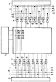
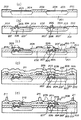
本発明の第1の実施形態を、図1を参照しつつ詳細に説明する。図1は本実施形態に用いる液晶表示装置に用いられる液晶パネルの周辺回路部付近の説明図の一例である。図において、2は水平のシフトレジスタである。8は図上、上部に液晶パネル自体を配置した信号線、41−44はアナログビデオ入力線で本実施形態は4相で入力している。また、6はアナログビデオ入力線41−44を信号線8へ伝達するためのアナログスイッチで、本実施形態の例ではCMOSトランスファーゲートであるが、これに限定されないのは言うまでもない。また、51,52,53,54はアナログビデオ入力線41−44とアナログスイッチ6を接続する垂直配線で、52はアナログビデオ入力線41,42,43をジャンプしてアナログスイッチ6のドレインに接続されている。53は同様にアナログビデオ入力線41をジャンプしてアナログスイッチのドレインに接続されている。54は同様にアナログビデオ入力線41,42をジャンプしてアナログスイッチ6のドレインに接続されている。それに対して51はアナログビデオ入力線をジャンプせずアナログスイッチ6と接続することが可能である。
【0027】
ここで、本実施形態ではアナログビデオ入力線41−44とアナログスイッチ6との接続距離が最も大きいアナログビデオ入力線はアナログビデオ入力線44であって垂直配線52に対応し、一方最も小さいのはアナログビデオ入力線41であり、垂直配線51に対応する。図1上左から垂直配線の長さを示すと1:4:2:3となり、順序正しく並べていない。この場合、順次の垂直配線に対して接続距離に対応した各抵抗値が異なる等から、画質のばらつきを見にくくする効果がある。本実施形態では4相アナログビデオ入力でXGAパネルに適応した場合であるが、許される1画素への書き込み時間はおよそ51nsと短い。この時上記ジャンプによる垂直配線材の寄生する信号線容量Cと抵抗RによるディレイCRは、本実施形態ではポリシリコン配線を用いており、アナログビデオ入力線41−44とアナログスイッチ6との接続距離が最短の51垂直配線でポリシリコン抵抗がR=120Ω、信号線容量がC=6.0pF,で、CR=0.7ns,アナログビデオ入力線41−44とアナログスイッチ6の最長の52垂直配線でC=6.0pF,R=731Ωで、CR=4.4nsとそれぞれで大きく異なる。
【0028】
実際はアナログスイッチ6のオン抵抗も加味されるが、このディレイと抵抗値によって、信号線に書き込まれる電圧が各信号線によって異なってしまい、結局各画素に書き込まれる電圧がそれぞれ異なり、画質上のむらが生じてしまう。特にその電圧差が順序良く並んでいる場合は、人間の目には敏感に感じてしまい、画質的には見づらいものとなってしまう。一方、本実施形態のように、この電圧差が順序良く並んでいない場合は、人間の目の感度は鈍くなり、画質的に満足するものとなる。図1では一例としてアナログビデオ入力線41−44とアナログスイッチ6との接続距離の最短と最長が並んでいる形の例で示しており、この場合でも順序正しく並んでいる場合に比べて画質的に大きな効果があるが、この配列に特に限定されない。例えば奇数と偶数に分け、1→3→2→4等の例でもよく、4本の信号線の組以外でも、複数本の信号線の場合でも、まずは最短と最長の接続距離を持たせることで、バラツキを目立たせなくできる。
【0029】
本実施形態ではXGAパネルで示したが、画素数が多くなればなるほど、この書き込み特性への要求は厳しく、画素書き込み電位のばらつきは大きくなる。アナログビデオ入力線を増加すれば、書き込み時間は余裕ができるが、ジャンプ距離が伸びるため、アナログビデオ入力線とアナログスイッチとの接続距離による画素書き込み電位のばらつきは大きくなる。アナログビデオ入力線とアナログスイッチとの接続距離に関しては、CR(容量×抵抗)として画像表示特性に影響を及ぼすので、液晶への印加電圧によらず、本質的な問題であるといえる。また本実施形態ではアナログビデオ入力線とアナログスイッチとの接続はPoly−Si材料を使用している。これは一例であり、他のW等のポリサイド材料、メタルでも特に問題はないことは言うまでもない。例えば、メタルではAL,ALSiCu,AlGeCu,AlCu,AlC以外にCr,Au,Ag等の材料を使用することが可能である。このような材料を使用することにより、抵抗値が低く、配線がアナログビデオ入力線を超える場合においてもCRで決められるディレイが小さくなり、画素への書き込みが安定に、ばらつきが少なく行える。
【0030】
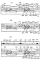
[第2の実施形態]
本発明の第2の実施形態を図2を参照しつつ詳細に説明する。図2は本実施形態に用いる液晶表示装置に用いられる液晶パネルの周辺回路部付近の説明図の一例である。図において、1は基板上に形成された液晶パネル、2は水平のシフトレジスタ、3は垂直のシフトレジスタである。また、8はアナログビデオ信号線の一体総称、41−48はアナログビデオ入力線で、本実施形態は上下4相、全8相で入力している。また、6はアナログビデオ入力線8を信号線へ伝達するためのアナログスイッチで、本実施形態の例ではCMOSトランスファーゲートであるが、これに限定されないのは言うまでもない。さらに、51−58はアナログビデオ入力線とアナログスイッチを接続する垂直配線で、51−54は第1の実施形態の部分と同様である。この上下の水平シフトレジスタでアナログスイッチ6を介してドライブされる液晶画素は、図のように、上下で1ライン毎に相互にドライブされる。この部分の4本の対として、左からアナログビデオ入力線とアナログスイッチとの接続距離垂直配線の長さを示すと、1,4,2,3となり、順序正しく並べていない。
【0031】
こうすることにより、画質のばらつきを見にくくなる効果がある。さらに本実施形態では、55−58で示される上部水平シフトレジスタ用の配線で示す、アナログビデオ入力線とアナログスイッチとの接続距離は左から短い順に4,2,3,1となっており、上下で順序が一つずれて異なることに大きな特徴がある。こうすることによって、例えば図2で示すような同じ画素ラインで画素A,C,E,G,…に書き込まれる電圧が異なり、縦筋になり難くなる。8つの画素でそれぞれかかれる電圧差が多少あったとしても、人間の目の感度は区別できずに鈍くなり、画質的に満足するものとなる。さらに第1の実施形態の発明と組み合わせるとさらに効果が上がることは言うまでもない。本実施形態ではXGAパネルで示したが、画素数が多くなればなるほど、この書き込み特性への要求は厳しく、画素書き込み電位のばらつきは大きくなるので、本発明の方法は有効になる。
【0032】
さらに、図3は本実施形態に用いる液晶表示装置に用いられる液晶パネルの周辺回路部付近の説明図の一例である。図において、101−103はアナログビデオ入力線41−44間にレイアウトされた電源である。本実施形態では全てグラウンドに固定された基準電位の電源ラインであるが、各アナログビデオ入力線41−44間に基準電位を配置することで寄生容量を減少することができ、電源ラインに限定されることなく、ある一定電位に固定された配線ならば問題はない。さらには、電圧が変化する配線であっても、アナログビデオ入力線の電圧が変化しない、例えばブランキング期間に変化するような配線であっても同様に構わない。このようにアナログビデオ入力線間に固定電位の配線をレイアウトすることによって、アナログビデオ入力線の電圧変化が隣のアナログビデオ入力線同士で擾乱を受けることを防ぐことができ、安定したアナログビデオ入力電圧を実現できた。
【0033】
従って、信号線を通して画素に書き込まれる電圧も安定し、良好な表示特性を示す液晶表示装置が実現した。さらに本実施形態ではアナログビデオ入力線間に、ある一定電位に固定された配線を有する構造であるが、アナログビデオ入力線外側にも同様なある一定電位に固定された配線があってもよく、そうすると他クロックからの容量結合による電圧変化もシールドできるために好ましいことは言うまでもない。
【0034】
[第3の実施形態]
本発明の第3の実施形態を図4を参照しつつ詳細に説明する。図4は本発明を用いた液晶表示装置に用いられる液晶パネルの周辺回路部付近の説明図の一例である。本実施形態では、1は画素スイッチのTFT(Thin Film Transistor)及び液晶を有する画素部である。また、2は水平のシフトレジスタ、3は垂直のシフトレジスタである。8は信号線、9は駆動線、41−43はアナログビデオ入力線で、本実施形態はアナログビデオ信号を3相で入力している。6は水平シフトレジスタ2からのオンオフ信号でアナログビデオ入力線41−43を信号線8へ伝達するためのアナログスイッチで、本実施形態の例ではCMOSトランスファーゲートであるが、これに限定されないのは言うまでもない。
【0035】
また、51,52,53はアナログビデオ入力線41−43とアナログスイッチ6を接続する垂直配線で、52はアナログビデオ入力線41をジャンプしてアナログスイッチ6のドレインに接続されている。53は同様にアナログビデオ入力線41及び42をジャンプしてアナログスイッチ6のドレインに接続されている。それに対して51はアナログビデオ入力線をジャンプせずアナログスイッチ6と接続することが可能である。さらに、7はアナログビデオ入力線の容量を均一にする目的でそれぞれ51,52に付加的に接続されている付加配線である。本実施形態では3相アナログビデオ入力でXGAパネルに適応した場合であるが、許される1画素への書き込み時間はおよそ38nsと短い。
【0036】
この時、付加配線の存在で、アナログビデオ入力線容量はアナログヒデオ入力線41と43でそれぞれ最大値で75.3pF,75.5pFとほぼ均一に設計でき、良好な表示特性の液晶表示装置が実現できた。一方付加配線7が存在しない場合はそれぞれ、アナログビデオ入力線容量は60.9pF,67.5pFと10%ほどアナログビデオ入力線容量が異なってしまう。このような状況で、書き込みを行うと各画素間での電圧が異なり、表示として、むら、もしくは筋のような画像劣化となって現れてしまう。本実施形態ではXGAパネルで示したが、画素数が多くなればなるほど、この書き込み特性への要求は厳しく、ばらつきは大きくなる。アナログビデオ入力線を増加すれば、書き込み時間は余裕ができるが、ジャンプ距離が伸びるため、各アナログビデオ入力線容量の容量差は大きくなる。
【0037】
特に、アナログビデオ入力線容量に関しては、CR(容量×抵抗)として画像表示特性に影響を及ぼすので、液晶への印加電圧によらず、本質的な問題であるといえる。またさらに第1,第2の実施形態の発明と組み合わせるとさらに効果が上がることは言うまでもない。
【0038】
また、図5に本実施形態の他の構成例を示す。図5においては、図4とはビデオ入力線41〜43から配線順ではなく、アナログビデオ入力線41−43とアナログスイッチ6との接続距離の最短と最長が並んでいる形の例であり、且つスイッチ6までの各配線には最長の配線と同一長となるように付加配線7が施されており、この場合でも順序正しく並んでいる場合に比べて、画質的に大きな効果がある。なお、図上、この配列に特に限定されないのは勿論である。
【0039】
[第4の実施形態]
上述のアナログビデオ入力線と液晶パネル間のアナログビデオ信号用配線を用いた液晶装置について、説明する。
【0040】
以下に、本発明の実施形態を複数の液晶パネルを挙げて記述するが、それぞれの形態に限定されるものではない。相互の形態の技術を組み合わせることによって効果が増大することはいうまでもない。また、液晶パネルの構造は、半導体基板を用いたもので記述しているが、必ずしも半導体基板に限定されるものはなく、通常の透明基板上に以下に記述する構造体を形成してもいいし、本実施形態で述べる反射型液晶表示装置に限らず、透過型液晶表示装置でも構わないのはいうまでもない。また、以下に記述する液晶パネルは、すべてMOSFETやTFT型であるが、ダイオード型などの2端子型であってもいい。さらに、以下に記述する液晶パネルは、家庭用テレビはもちろん、プロジェクタ、ヘッドマウントディスプレイ、3次元映像ゲーム機器、ラップトップコンピュータ、電子手帳、テレビ会議システム、カーナビゲーション、飛行機のパネルなどの表示装置として有効である。
【0041】
本発明の液晶パネル部の断面を図6に示す。図において、301は半導体基板、302,302′はそれぞれp型及びn型ウェル、303,303′,303″はトランジスタのソース領域、304はゲート領域、305,305′,305″はドレイン領域である。
【0042】
図6に示すように、表示領域のトランジスタは、20〜35Vという高耐圧が印加されるため、ゲート304に対して、自己整合的にソース、ドレイン層が形成されず、オフセットをもたせ、その間にソース領域303′,ドレイン領域305′に示す如く、pウェル中の低濃度のn− 層,nウェル中の低濃度のp− 層が設けられる。ちなみにオフセット量は0.5〜2.0μmが好適である。一方、周辺回路の一部の回路部が図9の左側に示されているが、周辺部の一部の回路は、ゲートに自己整合的にソース、ドレイン層が形成されている。
【0043】
ここでは、ソース、ドレインのオフセットについて述べたが、それらの有無だけでなく、オフセット量をそれぞれの耐圧に応じて変化させたり、ゲート長の最適化が有効である。これは、周辺回路の一部は、ロジック系回路であり、この部分は、一般に1.5〜5V系駆動でよいため、トランジスタサイズの縮小及び、トランジスタの駆動力向上のため、上記自己整合構造が設けられている。本基板301は、p型半導体からなり、基板は、最低電位(通常は、基準電位の接地電位)であり、n型ウェルは、表示領域の場合、画素に印加する電圧すなわち20〜35Vがかかり、一方、周辺回路のロジック部は、ロジック駆動電圧1.5〜5Vが印加される。この構造により、それぞれ電圧に応じた最適なデバイスを構成でき、チップサイズの縮小のみならず、駆動スピードの向上による高画素表示が実現可能になる。
【0044】
また、図6において、306はフィールド酸化膜、310はデータ配線につながるソース電極、311は画素電極につながるドレイン電極、312は反射鏡を兼ねる画素電極、307は表示領域、周辺領域を覆う遮光層で、Ti,TiN,W,Mo等が適している。図6に示すように、上記遮光層307は、表示領域では、画素電極312とドレイン電極311との接続部を除いて覆っているが、周辺画素領域では、一部ビデオ線、クロック線等、配線容量が重くなる領域は、上記遮光層307をのぞき、照明光の光が混入し、回路の誤動作を起こす場合は画素電極312の層を覆う設計になっていて転送可能な工夫がなされている。さらに、308は遮光層307の下部の絶縁層で、P−SiO層318上にSOGにより平坦化処理を施し、そのP−SiO層318をさらに、P−SiO層308でカバーし、絶縁層308の安定性を確保した。SOGによる平坦化以外に、P−TEOS(Phospho−Tetraetoxy−Silane)膜を形成し、さらにP−SiO層318をカバーした後、絶縁層308をCMP処理し、平坦化する方法を用いても良いことは言うまでもない。
【0045】
また、309は反射電極312と遮光層307との間に設けられた絶縁層で、この絶縁層309を介して反射電極312の電荷保持容量となっている。大容量形成のために、SiO2 以外に、高誘電率のP−SiN、Ta2 O5 、やSiO2 との積層膜等が有効である。遮光層307に用いるTi,TiN,Mo,W等の平坦なメタル上に設ける事により、絶縁層309は、500〜5000オングストローム程度の膜厚が好適である。
【0046】
さらに、313は反射防止用膜、314は液晶材料、315は共通透明電極、316は対向基板、317,317′は高濃度不純物領域、319は表示領域、320は反射防止膜である。
【0047】
図6に示すように、トランジスタ下部に形成されたウェル302,302’と同一極性の高濃度不純物層317,317′は、ウェル302,302’の周辺部及び内容に形成されており、高振幅な信号がソースに印加されても、ウェル電位は、低抵抗層で所望の電位に固定されているため、安定しており、高品質な画像表示が実現できた。さらにn型ウェル302’とp型ウェル302との間には、フィールド酸化膜を介して上記p+型、n+型の高濃度不純物層317,317′が設けられており、通常MOSトランジスタの時に使用されるフィールド酸化膜直下のチャネルストップ層を不要にしている。
【0048】
これらのp+型、n+型高濃度不純物層317,317′は、ソース、ドレイン層形成プロセスで同時にできるので作製プロセスにおけるマスク枚数、工数が削減され、低コスト化が図れた。
【0049】
次に、313は共通透明電極315と対向基板316との間に設けられた反射防止用膜で、界面の液晶の屈折率を考慮して、界面反射率が軽減されるように構成される。その場合、対向基板316と、透過電極315の屈折率よりも小さい絶縁膜が好適である。
【0050】
次に、本発明の平面図を図7に示す。図において、321は水平シフトレジスタ、322は垂直シフトレジスタ、323はnチャンネルMOSFET、324はpチャンネルMOSFET、325は保持容量、326は液晶層、327は信号転送スイッチ、328はリセットスイッチ、329はリセットパルス入力端子、330はリセット電源端子、331は映像信号の入力端子である。半導体基板301は図7ではp型になっているが、n型でもよい。
【0051】
ウェル領域302’は、半導体基板301と反対の導電型にする。このため、図7では、ウェル領域302はp型になっている。p型のウェル領域302及びn型のウェル領域302′は、半導体基板301よりも高濃度に不純物が注入されていることが望ましく、半導体基板301の不純物濃度が1014〜1015(cm−3)のとき、ウェル領域302の不純物濃度は1015〜1017(cm−3)が望ましい。
【0052】
図6において、ソース電極310は、表示用信号が送られてくるデータ配線に、ドレイン電極311は画素電極312に接続する。これらの電極310,311には、通常Al,AlSi,AlSiCu,AlGeCu,AlCu配線を用いる。これらの電極310,311の下部と半導体との接触面に、TiとTiNからなるバイアメタル層を用いると、コンタクトが安定に実現できる。またコンタクト抵抗も低減できる。また、第1,第2の実施形態で説明した配線についても画素同士のドライブ遅延が発生しない構造とすることは勿論である。さらに、画素電極312は、表面が平坦で、高反射材が望ましく、通常の配線用金属であるAl,AlSi,AlSiCu,AlGeCu,AlC以外にCr,Au,Agなどの材料を使用することが可能である。また、平坦性の向上のため、下地絶縁層309や画素電極312の表面をケミカルメカニカルポリッシング(CMP)法によって処理している。
【0053】
図7における保持容量325は、画素電極312と共通透明電極315の間の信号を保持するための容量である。ウェル領域302には、基板電位を印加する。本実施形態では、各行のトランスミッションゲート構成を、上から1行目は上がnチャンネルMOSFET323で、下がpチャンネルMOSFET324、2行目は上がpチャンネルMOSFET324で、下がnチャンネルMOSFET323とするように、隣り合う行で順序を入れ換える構成にしている。以上のように、ストライプ型ウェルで表示領域の周辺で電源線とコンタクトしているだけでなく、表示領域にも、細い電源ラインを設けコンタクトをとっている。
【0054】
この時、ウェルの抵抗の安定化がカギになる。したがって、p型基板であれば、nウェルの表示領域内部でのコンタクト面積又はコンタクト数をpウェルのコンタクトより増強する構成を採用した。pウェルは、p型基板で一定電位がとられているため、基板が低抵抗体としての役割を演ずる。したがって、島状になるnウェルのソース、ドレインへの信号の入出力による振られの影響が大きくなりやすいが、それを上部の配線層からのコンタクトを増強することで防止できた。これにより、安定した高品位な表示が実現できた。
【0055】
映像信号(ビデオ信号、パルス変調されたデジタル信号など)は、映像信号入力端子331から入力され、水平シフトレジスタ321からのパルスに応じて信号転送スイッチ327を開閉し、各データ配線に出力する。垂直シフトレジスタ322からは、選択した行のnチャンネルMOSFET323のゲートへはハイパルス、pチャンネルMOSFETのゲートへはローパルスを印加する。
【0056】
以上のように、画素部のスイッチは、単結晶のCMOSトランスミッションゲートで構成されており、画素電極へ書き込む信号が、MOSFETのしきい値に依存せず、ソースへの信号をフルに書き込める利点を有する。
【0057】
又、スイッチが、単結晶トランジスタから成り立っており、polysi−TFTの結晶粒界での不安定な振まい等がなく、バラツキのない高信頼性な高速駆動が実現できる。
【0058】
次にパネル周辺回路の構成について、図8を用いて説明する。図8において、337は液晶素子の表示領域、332はレベルシフター回路、333はビデオ信号サンプリングスイッチ、334は水平シフトレジスタ、335はビデオ信号入力端子、336は垂直シフトレジスタである。
【0059】
ここでの水平、垂直SR334,336は、走査方向は選択スイッチにより双方向可能なものとなっており、光学系の配置等の変更に対して、パネルの変更なしに対応でき、製品の異なるシリーズにも同一パネルが使用でき、低コスト化が図れるメリットがある。又、図8においては、ビデオ信号サンプリングスイッチ333は、片側極性の1トランジスタ構成のものを記述したが、これに限らず、CMOSトランスミッションゲート構成にすることにより入力ビデオ線をすべてを信号線に書き込むことができることは、言うまでもない。勿論、この部分に、第1乃至第3の実施形態で用いた回路構成(レイアウト)を用いることで、良質な画質を得ることができる。
【0060】
又、CMOSトランスミッションゲート構成にした時、nMOSゲートとpMOSゲート面積や、ゲートとソース・ドレインとの重なり容量の違いにより、ビデオ信号に振られが生じる課題がある。これにはそれぞれの極性のサンプリングスイッチのMOSFETのゲート量の約1/2のゲート量のMOSFETのソースとドレインとを信号線にそれぞれ接続し、逆相パルスで印加することにより振られが防止でき、きわめて良好なビデオ信号が信号線に書き込まれた。これにより、さらに高品位の表示が可能になった。
【0061】
次に、ビデオ信号と、サンプリングパルスの同期を正確にとる方法について、図9を用いて説明する。このためには、サンプリングパルスのdelay量を変化させる必要がある。342はパルスdelay用インバータ、343はどのdelay用インバータを選択するかを決めるスイッチ、344はdelay量が制御された出力、345は容量であり、M1〜M11は各CMOS構成のドライバで、outBは入力に対する逆相出力、outは同相出力であり、346は保護回路である。
【0062】
また、SEL1(SEL1B)からSEL3(SEL3B)の組み合わせにより、delay用インバータ342を何個通過するかを選択できる。
【0063】
この同期回路をパネルに内蔵していることにより、パネル外部からのパルスのdelay量が、R.G.B3板パネルのとき、治具等の関係で対称性がくずれても、上記選択スイッチで調整でき、R,G,Bのパルス位相高域による位置ずれがない良好な表示画像が得られた。又、パネル内部に温度測定ダイオードを内蔵させ、その出力によりdelay量をテーブルから参照し温度補正することも有効である事は言うまでもない。
【0064】
次に、液晶材との関係について説明する。図6では、平坦な対向基板構造のものを示したが、共通電極基板316は、共通透明電極315の界面反射を防ぐため、凹凸を形成し、その表面に共通透明電極315を設けている。また、共通電極基板316の反対側には、反射防止膜320を設けている。これらの凹凸形状の形成のために、微少な粒径の砥粒により砂ずり研磨をおこなう方式も高コントラスト化に有効である。
【0065】
また、液晶材料としては、ポリマー・ネットワーク液晶PNLCを用いた。ただし、ポリマー・ネットワーク液晶として、PDLCなどを用いてもいい。ポリマー・ネットワーク液晶PNLCは、重合相分離法によって作製される。液晶と重合性モノマーやオリゴマーで溶液をつくり、通常の方法でセル中に注入した後、UV重合によって液晶と高分子を相分離させ、液晶中に網目状に高分子を形成する。PNLCは多くの液晶(70〜90wt%)を含有している。
【0066】
PNLCにおいては、屈折率の異方性(Δn)の高いネマチック液晶を用いると光散乱が強くない、誘電異方性(Δε)の大きいネマチック液晶を用いると、低電圧で駆動が可能となる。ポリマー・ネットワークの大きさ、すなわち網目の中心間距離が1〜1.5(μm)の場合、光散乱は高コントラストを得るのに十分強くなる。
【0067】
次に、シール構造と、パネル構造との関係について、図10を用いて説明する。図10において、351はシール部、352は電極パッド、353はクロックバッファー回路である。不図示のアンプ部は、パネル電気検査時の出力アンプとして使用するものである。また、対向基板の電位をとる不図示のAgペースト部があり、また、356は液晶素子による表示部、357は水平・垂直シフトレジスタ(H,VSR)等の周辺回路部である。シール部351は表示部356の四方周辺に、半導体基板301上に画素電極312を設けたものと、共通電極315を備えたガラス基板との張り合わせのための圧着材や接着剤の接触領域を示し、シール部351で張り合わせた後に、表示部356とシフトレジスタ部357に液晶を封入する。
【0068】
図10に示すように、本実施形態では、シールの内部にも、外部にも、total chip sizeが小さくなるように、回路が設けられている。本実施形態では、パッドの引き出しをパネルの片辺側の1つに集中させているが、長辺側の両辺でも又、一辺でなく多辺からのとり出しも可能で、高速クロックをとり扱うときに有効である。
【0069】
さらに、本発明のパネルは、Si基板等の半導体基板を用いているため、プロジェクタのように強力な光が照射され、基板の側壁にも光があたると、基板電位が変動し、パネルの誤動作を引き起こす可能性がある。したがって、パネルの側壁及び、パネル上面の表示領域の周辺回路部は、遮光できる基板ホルダーとなっており、又、Si基板の裏面は、熱伝導率の高い接着剤を介して熱伝導率の高いCu等のメタルが接続されたホルダー構造となっている。
【0070】
次に本発明のポイントである反射電極構造及びその作製方法について述べる。本発明の完全平坦化反射電極構造は、メタルをパターニングしてから、研磨する通常の方法とは異なり、電極パターンのところにあらかじめ、溝のエッチングをしておき、そこにメタルを成膜し、電極パターンが成形されない領域上のメタルを研磨でとり除くとともに、電極パターン上のメタルも平坦化する新規な方法である。しかも、配線の幅が配線以外の領域よりも極めて広く、従来のエッチング装置の常識では、下記問題が発生し、本発明の構造体は作製できない。
【0071】
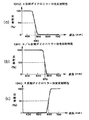
すなわち、エッチングすると、エッチング中にポリマーが堆積し、パターニングができなくなる。そこで、酸化膜系エッチング(CF4 /CHF3 系)において、条件を変えてみた(図11)。図11(a)に示すtotal圧力(従来)1.7torr時と、(b)に示すtotal圧力(今回)1.0torr時とした場合を示す。
【0072】
図11(a)の条件で、デポジション性のガスCHF3 をへらすと、たしかにポリマーの堆積は、減少するが、レジストに近いパターンと遠いパターンでの寸法の違い(ローディング効果)がきわめて大きくなり、使用できない事がわかる。
【0073】
図11(b)では、ローディング効果おさえるため、徐々に圧力を下げていき、1torr以下になるとローディング効果がかなり抑制され、かつCHF3 をゼロにし、CF4 のみによるエッチングが有効であることを見出した。
【0074】
さらに、画素電極領域は、ほとんどレジストが存在せず、周辺部にはレジストでしめられている。構造体を形成するのは難しく、構造として、画素電極と同等の空き電極とその形状を表示領域の周辺部まで設ける事が有効であることがわかった。
【0075】
本構造にすることにより、従来あった表示部と周辺部もしくはシール部との段差もなくなり、ギャップ精度が高くなり、面内均一圧が高くなるだけでなく、注入時のムラもへり、高品位の画質が歩留りよくできる効果が得られた。
【0076】
次に本発明の反射型液晶パネルを組み込む光学システムについて図12を用いて説明する。図12において、371はハロゲンランプ等の光源、372は光源像をしぼり込む集光レンズ、373,375は平面状の凸型フレネルレンズ、374はR,G,Bに分解する色分解光学素子で、ダイクロイックミラー、回折格子等が有効である。
【0077】
また、376はR,G,B光に分離されたそれぞれの光をR,G,B3パネルに導くそれぞれのミラー、377は集光ビームを反射型液晶パネルに平行光で照明するための視野レンズ、378はR,G,B毎の上述の反射型液晶素子、379の位置にしぼりがある。また、380は複数のレンズを組み合わせて拡大する投射レンズである。また、381はスクリーンで、通常、投射光を平行光へ変換するフレネルレンズと上下、左右に広視野角として表示するレンチキュラレンズの2板より構成されると明瞭な高コントラストで明るい画像を得ることができる。図12の構成では、1色の液晶パネルのみ記載されているが、色分解光学素子374からしぼり部379の間は3色それぞれに分離されており、3板パネルが配置されている。又、反射型液晶装置パネル表面にマイクロレンズアレーを設け、異なる入射光を異なる画素領域に照射させる配置をとることにより、3板のみならず、単板構成でも可能であることは言うまでもない。液晶素子の液晶層に電圧が印加され、各画素で正反射した光は、379に示すしぼり部を透過し、スクリーン上に投射される。
【0078】
一方、電圧が印加されずに、液晶層が散乱体となっている時、反射型液晶素子へ入射した光は、等方的に散乱し、379に示す絞り部の開口を見込む角度の中の散乱光以外は、投射レンズに入らない。これにより黒を表示する。以上の光学系からわかるように、偏光板が不要で、しかも画素電極の全面が信号光が高反射率で投射レンズにはいるため、従来よりも2−3倍明るい表示が実現できた。上述の実施形態でも述べたように、対向基板表面、界面には、反射防止対策が施されており、ノイズ光成分も極めて少なく、高コントラスト表示が実現できた。又、パネルサイズが小さくできるため、すべての光学素子(レンズ、ミラーetc.)が小型化され、低コスト、軽量化が達成された。
【0079】
又、光源の色ムラ、輝度ムラ、変動は、光源と光学系との間にインテグレタ(はえの目レンズ型ロッド型)を挿入することにより、スクリーン上での色ムラ、輝度ムラは、解決できた。
【0080】
上記液晶パネル以外の周辺電気回路について、図13を用いて説明する。図において、385は電源で、主にランプ用電源とパネルや信号処理回路駆動用システム電源に分離される。386はプラグ、387はランプ温度検出器で、ランプの温度の異常があれば、制御ボード388によりランプを停止させる等の制御を行う。これは、ランプに限らず、389のフィルタ安全スイッチでも同様に制御される。たとえば、高温ランプハウスボックスを開けようとした場合、ボックスがあかなくなるような安全上の対策が施されている。390はスピーカー、391は音声ボードで、要求に応じて3Dサウンド、サラウンドサウンド等のプロセッサも内蔵できる。392は拡張ボード1で、ビデオ信号用S端子、ビデオ信号用コンポジット映像、音声等の外部装置396からの入力端子及びどの信号を選択するかの選択スイッチ395、チューナ394からなり、デコーダ393を介して拡張ボード2へ信号が送られる。一方、拡張ボード2は、おもに、別系列からのビデオやコンピュータのDsub15ピン端子を有し、デコーダ393からのビデオ信号と切り換えるスイッチ450を介して、A/Dコンバータ451でディジタル信号に変換される。
【0081】
また、453は主にビデオRAM等のメモリとCPUとからなるメインボードである。A/Dコンバータ451でA/D変換したNTSC信号は、一端メモリに蓄積され、高画素数へうまく割りあてるために、液晶素子数にマッチしていない空き素子の不足の信号を補間して作成したり、液晶表示素子に適したγ変換エッジ階調、ブライト調整バイアス調整等の信号処理を行う。NTSC信号でなく、コンピュータ信号も、たとえばVGAの信号がくれば、高解像度のXGAパネルの場合、その解像度変換処理も行う。一画像データだけでなく、複数の画像データのNTSC信号にコンピュータ信号を合成させる等の処理もこのメインボード453で行う。メインボード453の出力はシリアル・パラレル変換され、ノイズの影響を受けにくい形態でヘッドボード454に充られる。このヘッドボード454で、再度パラレル/シリアル変換後、D/A変換し、パネルのビデオ線数に応じて分割され、ドライブアンプを介して、B,G,R色の液晶パネル455,456,457へ信号を書き込む。452はリモコン操作パネルで、コンピュータ画面も、TVと同様の感覚で、簡単操作可能となっている。また、液晶パネル455,456,457の夫々は、各色の色フィルタを備えた同一の液晶装置構成であり、その水平・垂直走査回路は第1〜第3の実施形態で説明したものを適用する。各液晶装置は以上の説明のように、必ずしも高解像度がない画像も処理により高品位画像化になるため、本発明の表示結果は、きわめてきれいな画像表示が可能である。
【0082】
[第5の実施形態]
図14に本発明の液晶表示装置を用いた前面及び背面投写型液晶表示装置光学系の構成図を示す。本図はその上面図を表す図14(a)、正面図を表す図14(b)、側面図を表す図14(c)から成っている。同図において、1301はスクリーンに投射する投影レンズ、1302はマイクロレンズ付液晶パネル、1303は偏光ビームスプリッター(PBS)、1340はR(赤色光)反射ダイクロイックミラー、1341はB/G(青色&緑色光)反射ダイクロイックミラー、1342はB(青色光)反射ダイクロイックミラー、1343は全色光を反射する高反射ミラー、1350はフレネルレンズ、1351は凸レンズ、1306はロッド型インテグレーター、1307は楕円リフレクター、1308はメタルハライド、UHP等のアークランプである。
【0083】
ここで、R(赤色光)反射ダイクロイックミラー1340、B/G(青色&緑色光)反射ダイクロイックミラー1341、B(青色光)反射ダイクロイックミラー1342はそれぞれ図15に示したような分光反射特性を有している。そしてこれらのダイクロイックミラーは高反射ミラー1343とともに、図16の斜視図に示したように3次元的に配置されており、後述するように白色照明光をRGBに色分解するとともに、液晶パネル1302に対して各原色光が、3次元的に異なる方向から該液晶パネル1302を照明するようにしている。
【0084】
ここで、光束の進行過程に従って説明すると、まず光源のランプ1308からの出射光束は白色光であり、楕円リフレクター1307によりその前方のインテグレータ1306の入り口に集光され、このインテグレーター1306内を反射を繰り返しながら進行するにつれて光束の空間的強度分布が均一化される。そしてインテグレーター1306を出射した光束は凸レンズ1351とフレネルレンズ1350とにより、x軸−方向(図14(b)の正面図基準)に平行光束化され、まずB反射ダイクロイックミラー1342に至る。このB反射ダイクロイックミラー1342ではB光(青色光)のみが反射され、z軸−方向つまり下側(図14(b)の正面図基準)にz軸に対して所定の角度でR反射ダイクロイックミラー1340に向かう。
【0085】
一方、B光以外の色光(R/G光)はこのB反射ダイクロイックミラー1342を通過し、高反射ミラー1343により直角にz軸−方向(下側)に反射され、やはりR反射ダイクロイックミラー1340に向かう。ここで、B反射ダイクロイックミラー1342と高反射ミラー1343は共に図14(a)の正面図を基にして言えば、インテグレーター1306からの光束(x軸−方向)をz軸−方向(下側)に反射するように配置しており、高反射ミラー1343はy軸方向を回転軸にx−y平面に対して丁度45°の傾きとなっている。それに対してB反射ダイクロイックミラー1342はやはりy軸方向を回転軸にx−y平面に対して、この45°よりも浅い角度に設定されている。
【0086】
従って、高反射ミラー1343で反射されたR/G光はz軸−方向に直角に反射されるのに対して、B反射ダイクロイックミラー1342で反射されたB光はz軸に対して所定の角度(x−z面内チルト)で下方向に向かう。ここで、B光とR/G光の液晶パネル1302上の照明範囲を一致させるため、各色光の主光線は液晶パネル1302上で交差するように、高反射ミラー1343とB反射ダイクロイックミラー1342のシフト量およびチルト量が選択されている。
【0087】
次に、前述のように下方向(z軸−方向)に向かったR/G/B光はR反射ダイクロイックミラー1340とB/G反射ダイクロイックミラー1341に向かうが、これらはB反射ダイクロイックミラー1342と高反射ミラー1343の下側に位置し、まず、B/G反射ダイクロイックミラー1341はx軸を回転軸にx−z面に対して45°傾いて配置されており、R反射ダイクロイックミラー1340はやはりx軸方向を回転軸にx−z平面に対してこの45°よりも浅い角度に設定されている。従ってこれらに入射するR/G/B光のうち、まずB/G光はR反射ダイクロイックミラー1340を通過して、B/G反射ダイクロイックミラー1341により直角にy軸+方向に反射され、PBS1303を通じて偏光化された後、x−z面に水平に配置された液晶パネル1302を照明する。このうちB光は前述したように(図14(a)、図14(b)参照)、x軸に対して所定の角度(x−z面内チルト)で進行しているため、B/G反射ダイクロイックミラー1341による反射後は、y軸に対して所定の角度(x−y面内チルト)を維持し、その角度を入射角(x−y面方向)として該液晶パネル1302を照明する。
【0088】
G光についてはB/G反射ダイクロイックミラー1341により直角に反射し、y軸+方向に進み、PBS1303を通じて偏光化された後、入射角0°つまり垂直に該液晶パネル1302を照明する。またR光については、前述のようにB/G反射ダイクロイックミラー1341の手前に配置されたR反射ダイクロイックミラー1340によりR反射ダイクロイックミラー1340にてy軸+方向に反射されるが、図14(c)(側面図)に示したようにy軸に対して所定の角度(y−z面内チルト)でy軸+方向に進み、PBS1303を通じて偏光化された後、該液晶パネル1302をこのy軸に対する角度を入射角(y−z面方向)として照明する。また、前述と同様にRGB各色光の液晶パネル1302上の照明範囲を一致させるため、各色光の主光線は液晶パネル1302上で交差するように、B/G反射ダイクロイックミラー1341とR反射ダイクロイックミラー1340のシフト量およびチルト量が選択されている。
【0089】
さらに、図15(a)に示したようにB反射ダイクロイックミラー1341のカット波長は480nm、図15(b)に示したようにB/G反射ダイクロイックミラー1341のカット波長は570nm、図15(c)に示したようにR反射ダイクロイックミラー1340のカット波長は600nmであるから、不要な橙色光はB/G反射ダイクロイックミラー1341を透過して捨てられる。これにより最適な色バランスを得ることができる。
【0090】
そして後述するように液晶パネル1302にて各RGB光は反射&偏光変調され、PBS1303に戻り、PBS1303のPBS面1303aにてx軸+方向に反射する光束が画像光となり、投影レンズ1301を通じて、スクリーン(不図示)に拡大投影される。ところで、該液晶パネル1302を照明する各RGB光は入射角が異なるため、そこから反射されてくる各RGB光もその出射角を異にしているが、投影レンズ1301としてはこれらを全て取り込むに十分な大きさのレンズ径及び開口のものを用いている。ただし、投影レンズ1301に入射する光束の傾きは、各色光がマイクロレンズを2回通過することにより平行化され、液晶パネル1302への入射光の傾きを維持している。
【0091】
ところが、図28に示したように従来例の透過型では、液晶パネルを出射した光束はマイクロレンズの集光作用分も加わってより大きく広がってしまうので、この光束を取り込むための投影レンズはさらに大きな開口数が求められ、高価なレンズとなっていた。しかし、本例では液晶パネル2からの光束の広がりはこのように比較的小さくなるので、より小さな開口数の投影レンズでもスクリーン上で十分に明るい投影画像を得ることができ、より安価な投影レンズを用いることが可能になる。また、図29に示す縦方向に同一色が並ぶストライプタイプの表示方式の例を本実施形態に用いることも可能であるが、後述するように、マイクロレンズを用いた液晶パネルの場合は好ましくない。
【0092】
次に、ここで用いる本発明液晶パネル1302について説明する。図17に該液晶パネル1302の拡大断面模式図(図16のy−z面に対応)を示す。図において、1321はマイクロレンズ基板、1322はマイクロレンズ、1323はシートガラス、1324は透明対向電極、1325は液晶層、1326は画素電極、1327はアクティブマトリックス駆動回路部、1328はシリコン半導体基板である。マイクロレンズ1322は、いわゆるイオン交換法によりガラス基板(アルカリ系ガラス)1321の表面上に形成されており、画素電極1326のピッチの倍のピッチで2次元的アレイ構造を成している。
【0093】
液晶層1325は反射型に適応したいわゆるDAP,HAN等のECBモードのネマチック液晶を採用しており、不図示の配向層により所定の配向が維持されている。第4の実施形態と比べると電圧値が低く、画素電極1326の電位の精度はさらに重要になってくるため、本発明の回路、構成は有効であり、単板で画素数も多く、従ってビデオ線の本数も多いため、第1乃至第3の実施形態の構成は非常に有効となる。画素電極1326はAlから成り、反射鏡を兼ねており、表面性を良くして反射率を向上させるため、パターニング後の最終工程でいわゆるCMP処理を施している(詳しくは後述する)。
【0094】
アクティブマトリックス駆動回路部1327はいわゆるシリコン半導体基板1328上に設けられた半導体回路であり、上記画素電極1326をアクティブマトリックス駆動するものであり、該回路マトリックスの周辺部には、不図示のゲート線ドライバー(垂直レジスター等)や信号線ドライバー(水平レジスター等)が設けられている(詳しくは後述する)。これらの周辺ドライバーおよびアクティブマトリックス駆動回路はRGBの各原色映像信号を所定の各RGB画素に書き込むように構成されており、該各画素電極1326はカラーフィルターは有さないものの、前記アクティブマトリックス駆動回路にて書き込まれる原色映像信号により各RGB画素として区別され、後述する所定のRGB画素配列を形成している。
【0095】
ここで、液晶パネル1302に対して照明するG光について見てみると、前述したようにG光はPBS1303により偏光化されたのち該液晶パネル1302に対して垂直に入射する。この光線のうち1つのマイクロレンズ1322aに入射する光線例を図中の矢印G(in/out)に示す。ここに図示されたように該G光線はマイクロレンズ1322により集光され、G画素電極1326g上を照明する。そしてAlより成る該画素電極1326gにより反射され、再び同じマイクロレンズ1322aを通じてパネル外に出射していく。このように液晶層1325を往復通過する際、該G光線(偏光)は画素電極1326gに印加される信号電圧により対向電極1324との間に形成される電界による液晶の動作により変調を受けて、該液晶パネルを出射し、PBS1303に戻る。
【0096】
ここで、その変調度合いによりPBS面1303aにて反射され、投影レンズ1301に向かう光量が変化し、各画素のいわゆる濃淡階調表示がなされることになる。一方、上述したように図中断面(y−z面)内の斜め方向から入射してくるR光については、やはりPBS1303により偏光されたのち、例えばマイクロレンズ1322bに入射するR光線に注目すると、図中の矢印R(in)で示したように、該マイクロレンズ1322bにより集光され、その真下よりも左側にシフトした位置にあるR画素電極1326r上を照明する。そして該画素電極1326rにより反射され、図示したように今度は隣(−z方向)のマイクロレンズ1322aを通じて、パネル外に出射していく(R(out))。
【0097】
この際、該R光線(偏光)はやはり画素電極1326rに印加される信号電圧により対向電極1324との間に形成される画像信号に応じた電界による液晶の動作により変調を受けて、該液晶パネルを出射し、PBS1303に戻る。そして、その後のプロセスは前述のG光の場合と全く同じように、画像光を投影レンズ1301から投影される。ところで、図17の描写では画素電極1326g上と画素電極1326r上の各G光とR光の色光が1部重なり干渉しているようになっているが、これは模式的に液晶層の厚さを拡大誇張して描いているためであり、実際には該液晶層の厚さは1〜5μであり、シートガラス1323の50〜100μに比べて非常に薄く、画素サイズに関係なくこのような干渉は起こらない。
【0098】
次に、図18に本例での色分解・色合成の原理説明図を示す。ここで、図18(a)は液晶パネル1302の上面模式図、図18(b)、図18(c)はそれぞれ該液晶パネル上面模式図に対するA−A′(x方向)断面模式図、B−B′(z方向)断面模式図である。ここで、マイクロレンズ1322は、図18(a)の一点鎖線に示すように、G光を中心として両隣接する2色画素の半分ずつに対して1個が対応している。このうち図18(c)はy−z断面を表す上記図17に対応するものであり、各マイクロレンズ1322に入射するG光とR光の入出射の様子を表している。これから判るように各G画素電極は各マイクロレンズの中心の真下に配置され、各R画素電極は各マイクロレンズ間境界の真下に配置されている。従ってR光の入射角はそのtanθが画素ピッチ(B&R画素)とマイクロレンズ・画素電極間距離の比に等しくなるように設定するのが好ましい。
【0099】
一方、図18(b)は該液晶パネル1302のx−y断面に対応するものである。このx−y断面については、B画素電極とG画素電極とが図18(c)と同様に交互に配置されており、やはり各G画素電極は各マイクロレンズ中心の真下に配置され、各B画素電極は各マイクロレンズ間境界の真下に配置されている。
【0100】
ところで該液晶パネルを照明するB光については、前述したようにPBS1303による偏光化後、図中断面(x−y面)の斜め方向から入射してくるため、R光の場合と全く同様に、各マイクロレンズ1322から入射したB光線は、図示したようにB画素電極1326bにより反射され、入射したマイクロレンズ1322に対して、x方向に隣り合うマイクロレンズ1322から出射する。B画素電極1326b上の液晶による変調や液晶パネルからのB出射光の投影については、前述のG光およびR光と同様である。
【0101】
また、各B画素電極1326bは各マイクロレンズ間境界の真下に配置されており、B光の液晶パネルに対する入射角についても、R光と同様にそのtanθが画素ピッチ(G&B画素)とマイクロレンズ・画素電極間距離の比に等しくなるように設定するのが好ましい。ところで、本例液晶パネルでは以上述べたように各RGB画素の並びがz方向に対してはRGRGRG…の並びに、x方向に対してはBGBGBG…の並びとなっているが、図18(a)はその平面的な並びを示している。このように各画素サイズは縦横共にマイクロレンズの約半分になっており、画素ピッチはx−z両方向ともにマイクロレンズのそれの半分になっている。また、G画素は平面的にもマイクロレンズ中心の真下に位置し、R画素はz方向のG画素間かつマイクロレンズ境界に位置し、B画素はx方向のG画素間かつマイクロレンズ境界に位置している。また、1つのマイクロレンズ単位の形状は矩形(画素の2倍サイズ)となっている。
【0102】
図19に本液晶パネルの部分拡大上面図を示す。ここで図中の破線格子1329は1つの絵素を構成するRGB画素のまとまりを示している。つまり、図17のアクティブマトリックス駆動回路部1327により各RGB画素が駆動される際、破線格子1329で示されるRGB画素ユニットは同一画素位置に対応したRGB映像信号にて駆動される。ここでR画素電極1326r、G画素電極1326g、B画素電極1326bから成る1つの絵素に注目してみると、まずR画素電極1326rは矢印r1で示されるようにマイクロレンズ1322bから前述したように斜めに入射するR光で照明され、そのR反射光は矢印r−2で示すようにマイクロレンズ1322aを通じて出射する。B画素電極1326bは矢印b1で示されるようにマイクロレンズ1322cから前述したように斜めに入射するB光で照明され、そのB反射光は矢印b2で示すようにやはりマイクロレンズ1322aを通じて出射する。またG画素電極1326gは正面後面矢印g12で示されるように、マイクロレンズ1322aから前述したように垂直(紙面奥へ向かう方向)に入射するG光で照明され、そのG反射光は同じマイクロレンズ1322aを通じて垂直に(紙面手前に出てくる方向)出射する。
【0103】
このように、本液晶パネルにおいては、1つの絵素を構成するRGB画素ユニットについて、各原色照明光の入射照明位置は異なるものの、それらの出射については、同じマイクロレンズ(この場合は1322a)から行われる。そしてこのことはその他の全ての絵素(RGB画素ユニット)についても成り立っている。
【0104】
従って、図20に示すように本液晶パネルからの全出射光をPBS1303および投影レンズ1301を通じて、スクリーン1309に投写するに際して、液晶パネル1302内のマイクロレンズ位置がスクリーン1309上に結像投影されるように光学調整すると、その投影画像は図22に示すようなマイクロレンズの格子内に各絵素を構成する該RGB画素ユニットからの出射光が混色した状態つまり同画素混色した状態の絵素を構成単位としたものとなる。そして、前述した図29による従来例のようないわゆるRGBモザイクが無い、質感の高い良好なカラー画像表示が可能となる。
【0105】
アクティブマトリックス駆動回路部1327は各画素電極1326の下に存在するため、図17の回路断面図上では絵素を構成する各RGB画素は単純に横並びに描かれているが、各画素FETのドレインは、図19に示したような2次元的配列の各RGB画素電極1326に接続している。
【0106】
ところで、本投写型液晶表示装置の駆動回路系についてその全体ブロック図を図21に示す。ここで、1310はパネルドライバーであり、RGB映像信号を極性反転し、かつ所定の電圧増幅をした液晶駆動信号を形成するとともに、対向電極1324の駆動信号、各種タイミング信号等を形成している。1312はインターフェースであり、各種映像及び制御伝送信号を標準映像信号等にデコードしている。また、1311はデコーダーであり、インターフェース1312からの標準映像信号をRGB原色映像信号及び同期信号に、即ち液晶パネル1302に対応した画像信号にデコード・変換している。1314はバラストである点灯回路であり、楕円リフレクター1307内のアークランプ1308を駆動点灯する。1315は電源回路であり、各回路ブロックに対して電源を供給している。1313は不図示の操作部を内在したコントローラーであり、上記各回路ブロックを総合的にコントロールするものである。このように本投写型液晶表示装置は、その駆動回路系は単板式プロジェクターとしては、ごく一般的なものであり、特に駆動回路系に負担を掛けることなく、前述したようなRGBモザイクの無い良好な質感のカラー画像を表示することができるものである。
【0107】
ところで図23に本実施形態における液晶パネルの別形態の部分拡大上面図を示す。ここでは、マイクロレンズ1322の1つは、画素R,G,Bの3つに対応して配されている。また、マイクロレンズ1322の中心真下位置にB画素電極1326bを配列し、それに対し左右方向にG画素1326gが交互に並ぶように、上下方向にR画素1326rが交互に並ぶように配列している。このように配列しても、絵素を構成するRGB画素ユニットからの反射光が1つの共通マイクロレンズから出射するように、B光を垂直入射、R/G光を斜め入射(同角度異方向)とすることにより、前例と全く同様な効果を得ることができる。また、さらにマイクロレンズ1322の中心真下位置にR画素を配列しその他の色画素を左右または上下方向にR画素に対してG,B画素を交互に並ぶようにしても良い。
【0108】
[第6の実施形態]
図24に本発明に係わる液晶パネルの第6の実施形態を示す。同図は本液晶パネル1320の部分拡大断面図である。前記第5の実施形態との相違点を述べると、まず対向ガラス基板としてシートガラス1323を用いており、マイクロレンズ1220については、シートガラス1323上に熱可塑性樹脂を用いたいわゆるリフロー法により形成している。さらに、非画素部にスペーサー柱1251を感光性樹脂のフォトリソグラフィーにて形成している。該液晶パネル1320の部分上面図を図25(a)に示す。
【0109】
この図24,図25から判るようにスペーサー柱1251は所定の画素のピッチでマイクロレンズ1220の角隅部の非画素領域に形成されている。このスペーサー柱1251を通るA−A′断面図を図25(b)に示す。このスペーサー柱1251の形成密度については10〜100画素ピッチでマトリックス状に設けるのが好ましく、シートガラス1323の平面性と液晶の注入性というスペーサー柱数に対して相反するパラメーターを共に満足するように設定する必要がある。また本実施形態では金属膜パターンによる遮光層1221を設けており、各マイクロレンズ境界部分からの漏れ光の進入を防止している。これにより、このような漏れ光による投影画像の彩度低下(各原色画像光の混色による)やコントラスト低下が防止される。従って本液晶パネル1320を用いて、本実施形態の如き液晶パネルを備えた投写型表示装置を構成することにより、さらにメリハリのある良好な画質が得られるようになる。
【0110】
上記第4乃至第6の実施形態で液晶パネルや投写型表示装置について説明したが、第1乃至第3の実施形態で示した液晶画素のドライブ用配線について、複数の信号線、例えばR,G,B各色用の入力アナログ信号線から水平・垂直シフトレジスタから各画素への配線線長や配線容量を一致させることで、正確な画像、高品位な画像を得ることができることは、容易に構成できる。
【0111】
【発明の効果】
以上説明したように、本発明によればアナログビデオ入力を複数有する液晶表示装置において、該半導体装置内にはアナログビデオ入力線が半導体装置の片側に3本以上有し、且つアナログビデオ入力線と画素アレイの間にはアナログビデオ信号を所望の信号線に伝達させるためのアナログスイッチを有し、該アナログビデオ入力線と該アナログスイッチとの接続距離の大小を順序正しくしない事によって、多少の画素電位のばらつきがあったとしても、良質な画質を得ることができる、液晶表示装置を提供することができた。
【0112】
アナログビデオ入力線が半導体装置の両側に各2本以上有する場合はさらに、該アナログビデオ入力線と該アナログスイッチとの接続距離の大小の順番が両側で異なることによって、多少の画素電位のばらつきがあったとしても、良質な画質を得ることができる、液晶表示装置を提供することができた。またアナログビデオ入力線と該アナログスイッチとの接続距離はそれぞれ複数のアナログビデオ入力線に対応して異なっていても、配線自体の長さを等しくすることで、画素電位を安定的に固定し、液晶にかかる電圧を精密に制御でき、上記の組み合わせでさらに良質な画質を得ることができる、液晶表示装置を提供することができた。
【0113】
さらに、本発明に関わる投写型液晶表示装置においては、マイクロレンズ付反射型液晶パネルとそれぞれ異なる方向から各原色光を照明する光学系等を用いて、1つの絵素を構成する1組のR,G,B画素からの液晶による変調後の反射光が同一のマイクロレンズを通じて出射するようにしたことにより、RGBモザイクの無い質感の高い良好なカラー画像投写表示が可能となる。
【0114】
また、各画素からの光束はマイクロレンズを2回通過してほぼ並行化されるので、開口数の小さい安価な投影レンズを用いてもスクリーン上で明るい投影画像を得ることが可能になる。
【図面の簡単な説明】
【図1】本発明の第1実施形態を表す概略的回路図である。
【図2】本発明の第2実施形態を表す概略的回路図である。
【図3】本発明の第2実施形態で使用した概略的回路図である。
【図4】本発明の第3実施形態を表す概略的回路図である。
【図5】本発明の第3実施形態を表す概略的回路図である。
【図6】本発明によるCMPにより製造される液晶素子の断面図である。
【図7】本発明による液晶装置の概略的回路図である。
【図8】本発明による液晶装置のブロック図である。
【図9】本発明による液晶装置の入力部のディレイ回路を含む回路図である。
【図10】本発明による液晶装置の液晶パネルの概念図である。
【図11】本発明による液晶装置の製造上のエッチング処理の良否を判断するグラフである。
【図12】本発明による液晶装置を用いた液晶プロジェクターの概念図である。
【図13】本発明による液晶プロジェクターの内部を示す回路ブロック図である。
【図14】本発明による投写型液晶表示装置の光学系の実施形態を示す全体構成図である。
【図15】本発明による投写型液晶表示装置の光学系に用いたダイクロイックミラーの分光反射特性図である。
【図16】本発明による投写型液晶表示装置の光学系の色分解照明部の斜視図である。
【図17】本発明による液晶パネルの一実施形態の断面図である。
【図18】本発明による液晶パネルの色分解・色合成の原理説明図である。
【図19】本発明による一実施形態の液晶パネルの部分拡大上面図である。
【図20】本発明による投写型液晶表示装置の投影光学系を示す部分構成図である。
【図21】本発明による投写型液晶表示装置の駆動回路系を示すブロック図である。
【図22】本発明による投写型液晶表示装置のスクリーン上投影像の部分拡大図である。
【図23】本発明による一実施形態の液晶パネルの部分拡大上面図である。
【図24】本発明による一実施形態の液晶パネルの部分拡大上面図である。
【図25】本発明による一実施形態の液晶パネルの部分拡大上面図と断面図である。
【図26】液晶装置の液晶パネルの製造工程上の断面図である。
【図27】液晶装置の液晶パネルの製造工程上の断面図である。
【図28】マイクロレンズ付き透過型液晶パネルの部分拡大断面図である。
【図29】マイクロレンズ付き透過型液晶パネルを用いた投写型液晶表示装置のスクリーン上投影像の部分拡大図である。
【符号の説明】
1 画素領域
2 水平シフトレジスタ
3 垂直シフトレジスタ
41〜48 アナログビデオ入力線
6 アナログスイッチ
7 付加配線
8 信号線
51〜54 配線
101〜103 電源
301 半導体基板
302,302’ p型及びn型ウェル
303,303’ ソース領域
304 ゲート領域
305,305’ ドレイン領域
306 LOCOS絶縁層
307 遮光層
308 PSG
309 プラズマSiN
310 ソース電極
311 連結電極
312 反射電極&画素電極
313 反射防止膜
314 液晶層
315 共通透明電極
316 対向電極
317,317’ 高濃度不純物領域
319 表示領域
320 反射防止膜
321,322 シフトレジスタ
323 nMOS
324 pMOS
325 保持容量
327 信号転送スイッチ
328 リセットスイッチ
329 リセットパルス入力端子
330 リセット電源端子
331 映像信号入力端子
332 昇圧レベルシフター
342 パルスdelay用インバータ
343 スイッチ
344 出力
345 容量
346 保護回路
351 シール部
352 電極パッド
353 クロックバッファー
371 光源
372 集光レンズ
373,375 フレネルレンズ
374 色分解光学素子
376 ミラー
377 視野レンズ
378 液晶装置
379 絞り部
380 投影レンズ
381 スクリーン
385 電源
386 プラグ
387 ランプ温度検出
388 制御ボード
389 フィルタ安全スイッチ
453 メインボード
454 液晶パネルドライブヘッドボード
455,456,457 液晶装置
1220 マイクロレンズ(リフロー熱ダレ式)
1251 スペーサー柱
1252 周辺シール部
1301 投影レンズ
1302 マイクロレンズ付液晶パネル
1303 偏光ビームスプリッター(PBS)
1306 ロッド型インテグレータ
1307 楕円リフレクター
1308 アークランプ
1309 スクリーン
1310 パネルドライバー
1311 デコーダー
1312 インターフェース回路
1314 バラスト(アークランプ点灯回路)
1320 マイクロレンズ付液晶パネル
1321 マイクロレンズガラス基板
1322 マイクロレンズ(インデックス分布式)
1323 シートガラス
1324 対向透明電極
1325 液晶
1326 画素電極
1327 アクティブマトリックス駆動回路部
1328 シリコン半導体基板
1329 基本絵素単位
1340 R反射ダイクロイックミラー
1341 B/G反射ダイクロイックミラー
1342 B反射ダイクロイックミラー
1343 高反射ミラー
1350 フレネルレンズ(第2コンデンサーレンズ)
1351 第1コンデンサーレンズ[0001]
BACKGROUND OF THE INVENTION
The present invention Liquid crystal display device for displaying images, characters, etc. using liquid crystal About.
[0002]
[Prior art]
With the recent information communication era, the need to display information is increasing more and more. At such times, the importance of display devices that communicate with image information is increasing. Among them, the liquid crystal display device is attracting attention because of its thinness and low power consumption, and has grown into a key industry that follows the semiconductor industry. The liquid crystal display device is currently mainly used in a notebook-size personal computer having a 12-inch size. In the future, it is considered that a liquid crystal display device having a larger screen size will be used not only as a personal computer but also as a workstation or a home television. However, as the screen size increases, not only does the manufacturing apparatus become expensive, but electrically strict characteristics are required to drive a large screen. For this reason, as the screen size increases, the manufacturing cost increases rapidly, for example, in proportion to the second power of the size.
[0003]
Therefore, recently, a front or back projection (projection) method in which a small liquid crystal display panel is produced and a liquid crystal image is optically enlarged and displayed has been attracting attention. This is because the size can be reduced, the characteristics can be improved, and the cost can be reduced at the same time as the scaling rule that improves the performance and cost as the semiconductor becomes finer. From these points, when the liquid crystal display panel is a TFT type, a TFT having a small size and sufficient driving force is required, and the TFT is also shifting from one using amorphous Si to one using polycrystalline Si. An image signal of a resolution level such as the NTSC standard used for a normal television does not require a very high speed processing.
[0004]
Therefore, not only the TFT but also a peripheral drive circuit such as a shift register or a decoder can be manufactured from polycrystalline Si, and a liquid crystal display device in which the display area and the peripheral drive circuit are integrated can be obtained. However, even in polycrystalline Si, it does not reach single crystal Si, but is displayed in a high-definition television having a resolution level higher than that of the NTSC standard, an XGA (eXtended Graphics Array) or SXGA (Super eXtended Graphics Array) class. If it is going to implement | achieve, a shift register etc. must be divided and arranged in multiple. In this case, noise called ghost is generated in the display area corresponding to the division joint, and a countermeasure for solving the problem is desired in this field.
[0005]
On the other hand, a display device using a single crystal Si substrate, which has a much higher driving force than a display device having an integral structure of polycrystalline Si, has attracted attention. In this case, since the driving power of the transistors of the peripheral driving circuit is satisfactory, it is not necessary to perform the divided driving as described above. For this reason, problems such as noise can be solved.
[0006]
Whether these are polycrystalline Si or single crystal Si, the TFT drain and the reflective electrode are connected, and a liquid crystal is sandwiched between the reflective electrode and the transparent common electrode to form a reflective liquid crystal element. A reflective liquid crystal device in which a horizontal / vertical shift register for scanning the liquid crystal element is formed on a semiconductor substrate can be provided.
[0007]
[Problems to be solved by the invention]
The present applicant has filed Japanese Patent Application No. 7-186473 for a method of manufacturing a reflective liquid crystal device using the polycrystalline Si and single crystal Si as a semiconductor substrate. The application includes the following objects, solutions and examples.
[0008]
For that purpose, when light is incident on the pixel electrode of a conventional liquid crystal pixel, the incident light is scattered in all directions by the surface irregularities, and the light reflection efficiency becomes very small. In the alignment film rubbing process, it causes alignment failure, resulting in liquid crystal alignment failure, the image quality of the display image is deteriorated due to the decrease in contrast, and the groove portion between each pixel electrode is not rubbed. At the same time as the cause of alignment failure, along with the surface irregularities, a horizontal electric field is generated between the pixel electrodes, causing bright lines. The generation of the bright line significantly deteriorates the contrast of the displayed image and lowers the image quality. Therefore, the object of the present application is to solve the above problems, eliminate the unevenness on the surface of the pixel electrode, and cause the alignment defect and irregular reflection caused by the unevenness. It is an object to provide a liquid crystal display device and a method for manufacturing the same, which can prevent display and display images with high image quality.
[0009]
As a means for solving the problem, the liquid crystal display device of the present application is an active matrix liquid crystal display device in which a liquid crystal is sandwiched between an active matrix substrate in which a switching transistor is arranged for each pixel and a counter electrode substrate. The surface of all the pixel electrodes is coplanar and parallel to the active matrix substrate, and at least a part of the side wall of each pixel electrode is in contact with the insulator. In the present application, since the pixel electrode surface is formed by polishing by using chemical mechanical polishing (hereinafter referred to as “CMP”), the pixel electrode surface is formed into a mirror-like surface at the same time. All pixel electrode surfaces can be formed on the same plane. Furthermore, the pixel electrode layer is formed on the insulating layer, or the insulating layer is formed on the pixel electrode layer on which the hole is formed, and the polishing process is performed, so that the insulating layer is more favorable between the pixel electrodes. It is buried and completely uneven. Therefore, irregular reflection and alignment failure caused by the unevenness are prevented, and high-quality image display is possible.
[0010]
Further, as an example thereof, description will be given with reference to FIGS. 26 and 27. FIG. As a first embodiment, a reflective liquid crystal display device will be described. The manufacturing process of the active matrix substrate and the sectional view of the liquid crystal element are shown in FIGS. Hereinafter, this embodiment will be described in detail in order. Although FIG. 26 and FIG. 27 show the pixel portion, a peripheral drive circuit such as a shift register for driving the switching transistor of the pixel portion can be formed on the same substrate simultaneously with the pixel portion formation step. .
[0011]
Impurity concentration is 10 15 cm -3 The following n-type
[0012]
Then phosphorus 10 20 cm -3 After the
[0013]
Next, a PSG (phosphosilicate glass: oxide film doped with phosphorus) 208 as an interlayer film was formed on the entire surface of the
[0014]
A
[0015]
Using the plasma SiN210 as a dry etching stopper layer, the
[0016]
A
[0017]
The surface of the
[0018]
The active matrix substrate formed by the above steps further forms an
[0019]
Hereinafter, a method for driving the reflective liquid crystal element of this example will be briefly described. A signal potential is applied to the
[0020]
As apparent from FIG. 27H, the active matrix substrate of this example is formed on the surface of the
[0021]
However, in the liquid crystal display device of the above application, it is not easy to make the pixel potentials completely coincide with each other. That is, due to various factors such as a difference in circuit constants until writing to each pixel and process variations within a chip, some variation occurs even in adjacent pixels. Especially when the video signal is divided and given, the difference in the small time constant of each video signal wiring affects the image quality itself, that is, the subtle difference in pixel potential is As it feels very sensitive. The important thing is not to design the circuit so that each pixel potential has the same characteristics as possible, but also on a circuit that does not deteriorate the image quality even if there is some variation in each pixel electrode potential. It is a conclusion obtained as a result of diligent efforts by the inventors.
[0022]
Accordingly, the present invention provides a liquid crystal display device in which the pixel potential is stably fixed as much as possible, the voltage applied to the liquid crystal can be precisely controlled, and even if there is some variation in the pixel potential, a high quality image can be obtained. The purpose is to provide.
[0023]
[Solving the problem in order to means】
The present invention has the above object. Achievement To do A liquid crystal display device that divides an analog video signal into three or more analog video signal lines and applies the same to a liquid crystal panel, wherein the liquid crystal panel includes a liquid crystal pixel and a switching transistor for driving the liquid crystal pixel in a horizontal direction and a vertical direction. The horizontal switching transistors are commonly connected by gate lines, the vertical switching transistors are commonly connected by vertical wiring, and a potential for turning on the horizontal switching transistors is gated. An active matrix circuit that drives a liquid crystal pixel connected to a switching transistor on the row by applying a line to the row, and the three or more analog video signal lines are each analog A switch on the selected row connected to the vertical wiring via a switch Connection distance in the vertical wiring between the analog switch on the vertical lines connecting the transistor and the analog video input line, in the liquid crystal adjacent pixels in the horizontal direction on the selected row, the Connection distance is not sorted , It is characterized by that.
[0026]
DETAILED DESCRIPTION OF THE INVENTION
[First Embodiment]
A first embodiment of the present invention will be described in detail with reference to FIG. FIG. 1 is an example of an explanatory view in the vicinity of a peripheral circuit portion of a liquid crystal panel used in the liquid crystal display device used in this embodiment. In the figure, 2 is a horizontal shift register. 8 is a signal line in which the liquid crystal panel itself is arranged in the upper part of the figure, 41-44 are analog video input lines, and in this embodiment, they are input in four phases.
[0027]
Here, in this embodiment, the analog video input line having the longest connection distance between the analog
[0028]
Actually, the on-resistance of the
[0029]
In the present embodiment, an XGA panel is shown. However, as the number of pixels increases, the requirement for the writing characteristics becomes more severe, and the variation in pixel writing potential increases. If the number of analog video input lines is increased, the writing time can be afforded, but the jump distance is extended, so that the variation in the pixel writing potential due to the connection distance between the analog video input line and the analog switch increases. Since the connection distance between the analog video input line and the analog switch affects the image display characteristics as CR (capacitance × resistance), it can be said that this is an essential problem regardless of the voltage applied to the liquid crystal. In the present embodiment, a Poly-Si material is used for connection between the analog video input line and the analog switch. This is merely an example, and it goes without saying that there is no particular problem with other polycide materials such as W and metal. For example, in the case of metal, it is possible to use materials such as Cr, Au, and Ag in addition to AL, ALSiCu, AlGeCu, AlCu, and AlC. By using such a material, even when the resistance value is low and the wiring exceeds the analog video input line, the delay determined by CR becomes small, and writing to the pixel can be performed stably and with little variation.
[0030]
[Second Embodiment]
A second embodiment of the present invention will be described in detail with reference to FIG. FIG. 2 is an example of an explanatory view in the vicinity of a peripheral circuit portion of a liquid crystal panel used in the liquid crystal display device used in this embodiment. In the figure, 1 is a liquid crystal panel formed on a substrate, 2 is a horizontal shift register, and 3 is a vertical shift register.
[0031]
This has the effect of making it difficult to see variations in image quality. Furthermore, in this embodiment, the connection distance between the analog video input line and the analog switch, indicated by the wiring for the upper horizontal shift register indicated by 55-58, is 4, 2, 3, 1 in order from the left, The main feature is that the order is different by one up and down. By doing so, for example, the voltages written to the pixels A, C, E, G,... In the same pixel line as shown in FIG. Even if there are some voltage differences applied to each of the eight pixels, the sensitivity of the human eye is indistinguishable and becomes dull, and the image quality is satisfactory. Further, it goes without saying that the effect is further improved when combined with the invention of the first embodiment. In the present embodiment, the XGA panel is shown. However, as the number of pixels increases, the requirement for the write characteristics becomes more severe, and the variation in pixel write potential becomes larger. Therefore, the method of the present invention is effective.
[0032]
Furthermore, FIG. 3 is an example of an explanatory view in the vicinity of a peripheral circuit portion of a liquid crystal panel used in the liquid crystal display device used in this embodiment. In the figure, 101-103 is a power source laid out between the analog video input lines 41-44. In this embodiment, the power source line is a reference potential that is fixed to the ground. However, by arranging the reference potential between the analog video input lines 41-44, the parasitic capacitance can be reduced, and the power source line is limited to the power source line. There is no problem if the wiring is fixed at a certain constant potential. Furthermore, even if the wiring changes in voltage, the wiring in which the voltage of the analog video input line does not change, for example, changes in the blanking period may be used. By laying out a fixed-potential wiring between analog video input lines in this way, it is possible to prevent the change in voltage of the analog video input line from being disturbed between adjacent analog video input lines, and stable analog video input The voltage could be realized.
[0033]
Therefore, the voltage written to the pixel through the signal line is stabilized, and a liquid crystal display device having good display characteristics is realized. Furthermore, in this embodiment, the analog video input line has a structure having wiring fixed at a certain constant potential, but there may be a similar wiring fixed at a certain potential outside the analog video input line, In this case, it is needless to say that voltage changes due to capacitive coupling from other clocks can be shielded.
[0034]
[Third Embodiment]
A third embodiment of the present invention will be described in detail with reference to FIG. FIG. 4 is an example of an explanatory view in the vicinity of a peripheral circuit portion of a liquid crystal panel used in a liquid crystal display device using the present invention. In the present embodiment, reference numeral 1 denotes a pixel unit having a TFT (Thin Film Transistor) of a pixel switch and a liquid crystal.
[0035]
51, 52 and 53 connect the analog video input lines 41-43 and the
[0036]
At this time, due to the presence of the additional wiring, the analog video input line capacitance can be designed to be almost uniform with the analog
[0037]
In particular, the analog video input line capacitance is an essential problem regardless of the voltage applied to the liquid crystal because it affects the image display characteristics as CR (capacitance × resistance). Furthermore, it goes without saying that the effect is further improved when combined with the inventions of the first and second embodiments.
[0038]
FIG. 5 shows another configuration example of the present embodiment. In FIG. 5, FIG. 4 is an example in which the shortest and longest connection distances between the analog video input lines 41-43 and the
[0039]
[Fourth Embodiment]
A liquid crystal device using the above-described analog video signal wiring between the analog video input line and the liquid crystal panel will be described.
[0040]
Hereinafter, embodiments of the present invention will be described with reference to a plurality of liquid crystal panels, but the present invention is not limited to these embodiments. It goes without saying that the effect is increased by combining the technologies of each other. The structure of the liquid crystal panel is described using a semiconductor substrate. However, the structure is not necessarily limited to the semiconductor substrate, and the structure described below may be formed on a normal transparent substrate. Needless to say, the present invention is not limited to the reflective liquid crystal display device, and may be a transmissive liquid crystal display device. The liquid crystal panels described below are all of the MOSFET and TFT type, but may be a two-terminal type such as a diode type. Furthermore, the liquid crystal panels described below can be used as display devices for home TVs, projectors, head mounted displays, 3D video game machines, laptop computers, electronic notebooks, video conference systems, car navigation systems, airplane panels, etc. It is valid.
[0041]
A cross section of the liquid crystal panel of the present invention is shown in FIG. In the figure, 301 is a semiconductor substrate, 302 and 302 'are p-type and n-type wells, 303, 303' and 303 "are transistor source regions, 304 is a gate region, 305, 305 'and 305" are drain regions. is there.
[0042]
As shown in FIG. 6, since a high breakdown voltage of 20 to 35 V is applied to the transistor in the display region, the source and drain layers are not formed in a self-aligned manner with respect to the
[0043]
Although the source and drain offsets have been described here, it is effective to change not only the presence / absence of them but also the offset amount according to the respective breakdown voltage, or optimization of the gate length. This is because a part of the peripheral circuit is a logic system circuit, and this part may generally be driven by 1.5 to 5 V, so that the self-aligned structure is used to reduce the transistor size and improve the driving power of the transistor. Is provided. The
[0044]
In FIG. 6, 306 is a field oxide film, 310 is a source electrode connected to the data wiring, 311 is a drain electrode connected to the pixel electrode, 312 is a pixel electrode serving also as a reflecting mirror, 307 is a light shielding layer covering the display area and the peripheral area. Thus, Ti, TiN, W, Mo, etc. are suitable. As shown in FIG. 6, the
[0045]
[0046]
Further, 313 is an antireflection film, 314 is a liquid crystal material, 315 is a common transparent electrode, 316 is a counter substrate, 317 and 317 'are high-concentration impurity regions, 319 is a display region, and 320 is an antireflection film.
[0047]
As shown in FIG. 6, high-concentration impurity layers 317 and 317 ′ having the same polarity as the
[0048]
These p + Type, n + Since the high-concentration impurity layers 317 and 317 ′ can be formed simultaneously in the source and drain layer forming process, the number of masks and man-hours in the manufacturing process can be reduced, and the cost can be reduced.
[0049]
Next, reference numeral 313 denotes an antireflection film provided between the common
[0050]
Next, a plan view of the present invention is shown in FIG. In the figure, 321 is a horizontal shift register, 322 is a vertical shift register, 323 is an n-channel MOSFET, 324 is a p-channel MOSFET, 325 is a holding capacitor, 326 is a liquid crystal layer, 327 is a signal transfer switch, 328 is a reset switch, 329 is A reset pulse input terminal, 330 is a reset power supply terminal, and 331 is a video signal input terminal. Although the
[0051]
The
[0052]
In FIG. 6, the
[0053]
A
[0054]
At this time, stabilization of the resistance of the well is the key. Therefore, in the case of a p-type substrate, a configuration is adopted in which the contact area or the number of contacts inside the n-well display region is increased as compared with the p-well contact. Since the p-well has a constant potential on the p-type substrate, the substrate plays a role as a low resistance body. Therefore, the influence of fluctuation due to input / output of signals to the source and drain of the island-like n-well is likely to increase, but this can be prevented by increasing the contact from the upper wiring layer. As a result, stable and high-quality display was realized.
[0055]
A video signal (a video signal, a pulse-modulated digital signal, or the like) is input from a video
[0056]
As described above, the switch of the pixel portion is composed of a single crystal CMOS transmission gate, and the signal written to the pixel electrode does not depend on the threshold value of the MOSFET, and the advantage that the signal to the source can be written completely. Have.
[0057]
In addition, since the switch is formed of a single crystal transistor, there is no unstable behavior at the crystal grain boundary of the polysi-TFT, and high-speed driving with high reliability without variation can be realized.
[0058]
Next, the configuration of the panel peripheral circuit will be described with reference to FIG. In FIG. 8, 337 is a display area of the liquid crystal element, 332 is a level shifter circuit, 333 is a video signal sampling switch, 334 is a horizontal shift register, 335 is a video signal input terminal, and 336 is a vertical shift register.
[0059]
The horizontal and
[0060]
Further, when the CMOS transmission gate configuration is adopted, there is a problem that the video signal is shaken due to the difference in the nMOS gate and pMOS gate area and the overlap capacitance between the gate and the source / drain. This can be prevented by connecting the source and drain of a MOSFET whose gate amount is about ½ of the gate amount of the MOSFET of each polarity sampling switch to the signal line and applying it with a reverse-phase pulse. A very good video signal was written on the signal line. As a result, even higher quality display is possible.
[0061]
Next, a method for accurately synchronizing the video signal and the sampling pulse will be described with reference to FIG. For this purpose, it is necessary to change the delay amount of the sampling pulse. 342 is an inverter for pulse delay, 343 is a switch for determining which delay inverter is selected, 344 is an output whose delay amount is controlled, 345 is a capacitor, M1 to M11 are drivers of each CMOS configuration, and outB is An anti-phase output with respect to the input, out is an in-phase output, and 346 is a protection circuit.
[0062]
Further, it is possible to select how
[0063]
Since this synchronization circuit is built in the panel, the delay amount of the pulse from the outside of the panel is R.D. G. In the case of the B3 plate panel, even if the symmetry is lost due to the jig or the like, it can be adjusted by the selection switch, and a good display image without a positional shift due to the R, G, B pulse phase high region is obtained. Needless to say, it is also effective to incorporate a temperature measuring diode inside the panel and refer to the delay amount from the table to correct the temperature.
[0064]
Next, the relationship with the liquid crystal material will be described. Although FIG. 6 shows a flat counter substrate structure, the
[0065]
As the liquid crystal material, polymer network liquid crystal PNLC was used. However, PDLC or the like may be used as the polymer network liquid crystal. The polymer network liquid crystal PNLC is produced by a polymerization phase separation method. A solution is made of liquid crystal and a polymerizable monomer or oligomer, and injected into the cell by a normal method. Then, the liquid crystal and the polymer are phase-separated by UV polymerization to form a polymer in a network form in the liquid crystal. PNLC contains many liquid crystals (70-90 wt%).
[0066]
In PNLC, if nematic liquid crystal having a high refractive index anisotropy (Δn) is used, light scattering is not strong, and if nematic liquid crystal having a large dielectric anisotropy (Δε) is used, driving can be performed at a low voltage. When the size of the polymer network, that is, the distance between the centers of the meshes is 1 to 1.5 (μm), the light scattering is strong enough to obtain high contrast.
[0067]
Next, the relationship between the seal structure and the panel structure will be described with reference to FIG. In FIG. 10,
[0068]
As shown in FIG. 10, in this embodiment, a circuit is provided so that the total chip size is reduced both inside and outside the seal. In this embodiment, the pad drawer is concentrated on one side of the panel, but it is possible to take out from both sides of the long side, not from one side but from multiple sides, and handle a high-speed clock. Sometimes effective.
[0069]
Furthermore, since the panel of the present invention uses a semiconductor substrate such as a Si substrate, if the substrate is irradiated with strong light like the projector and light is also applied to the side wall of the substrate, the substrate potential fluctuates and the panel malfunctions. May cause. Therefore, the side wall of the panel and the peripheral circuit portion of the display area on the upper surface of the panel serve as a substrate holder capable of shielding light, and the back surface of the Si substrate has a high thermal conductivity through an adhesive having a high thermal conductivity. It has a holder structure to which a metal such as Cu is connected.
[0070]
Next, a reflective electrode structure and a manufacturing method thereof which are the points of the present invention will be described. Unlike the usual method of polishing after patterning the metal, the completely flattened reflective electrode structure of the present invention previously etched the groove at the electrode pattern, deposited the metal there, This is a novel method in which the metal on the region where the electrode pattern is not formed is removed by polishing and the metal on the electrode pattern is flattened. Moreover, the width of the wiring is much wider than the area other than the wiring, and the conventional problems of the conventional etching apparatus cause the following problems, and the structure of the present invention cannot be manufactured.
[0071]
That is, when etching is performed, a polymer is deposited during etching, and patterning cannot be performed. Therefore, oxide film etching (CF 4 / CHF 3 In the system), the conditions were changed (FIG. 11). FIG. 11A shows the case where the total pressure (conventional) is 1.7 torr and the case where the total pressure (current) is 1.0 torr shown in FIG.
[0072]
The deposition gas CHF under the conditions of FIG. 3 However, it can be seen that the deposition of the polymer decreases, but the dimensional difference (loading effect) between the pattern close to the resist and the pattern far from the resist becomes very large and cannot be used.
[0073]
In FIG. 11 (b), in order to suppress the loading effect, the pressure is gradually reduced, and when the pressure is 1 torr or less, the loading effect is considerably suppressed, and CHF 3 To zero, CF 4 It has been found that etching by only is effective.
[0074]
Further, the pixel electrode region has almost no resist, and the peripheral portion is covered with the resist. It was difficult to form a structure, and it was found effective to provide a blank electrode equivalent to the pixel electrode and its shape up to the periphery of the display area.
[0075]
By adopting this structure, there is no step between the conventional display part and the peripheral part or the seal part, the gap accuracy is increased, the in-plane uniform pressure is increased, and unevenness at the time of injection is reduced, resulting in high quality. The image quality can be improved.
[0076]
Next, an optical system incorporating the reflective liquid crystal panel of the present invention will be described with reference to FIG. In FIG. 12, 371 is a light source such as a halogen lamp, 372 is a condensing lens that squeezes the light source image, 373 and 375 are planar convex Fresnel lenses, and 374 is a color separation optical element that decomposes into R, G, and B. A dichroic mirror, a diffraction grating, etc. are effective.
[0077]
Reference numeral 376 denotes a mirror for guiding each light separated into R, G, and B light to the R, G, and B3 panels. Reference numeral 377 denotes a field lens for illuminating the reflected beam on the reflective liquid crystal panel with parallel light. Reference numeral 378 indicates the position of the above-described reflective
[0078]
On the other hand, when no voltage is applied and the liquid crystal layer is a scatterer, the light incident on the reflective liquid crystal element is scattered isotropically, and the angle within the angle at which the aperture of the aperture shown in 379 is viewed Except for scattered light, it does not enter the projection lens. As a result, black is displayed. As can be seen from the above optical system, a polarizing plate is not necessary, and the entire surface of the pixel electrode has a high reflectance of signal light, so that a display that is 2-3 times brighter than before can be realized. As described in the above embodiment, anti-reflection measures are taken on the surface and interface of the counter substrate, the noise light component is extremely small, and a high contrast display can be realized. Further, since the panel size can be reduced, all the optical elements (lenses, mirrors etc.) are miniaturized, and low cost and light weight are achieved.
[0079]
In addition, color unevenness, brightness unevenness, and fluctuations of the light source can be solved by inserting an integrator (a fly-eye lens rod type) between the light source and the optical system. did it.
[0080]
A peripheral electric circuit other than the liquid crystal panel will be described with reference to FIG. In the figure,
[0081]
A
[0082]
[Fifth Embodiment]
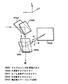
FIG. 14 shows a configuration diagram of a front and rear projection type liquid crystal display device optical system using the liquid crystal display device of the present invention. This figure consists of FIG. 14 (a) representing the top view, FIG. 14 (b) representing the front view, and FIG. 14 (c) representing the side view. In the figure, 1301 is a projection lens that projects on a screen, 1302 is a liquid crystal panel with a microlens, 1303 is a polarizing beam splitter (PBS), 1340 is an R (red light) reflecting dichroic mirror, and 1341 is B / G (blue and green). Light) reflective dichroic mirror, 1342 is a B (blue light) reflective dichroic mirror, 1343 is a highly reflective mirror that reflects all color light, 1350 is a Fresnel lens, 1351 is a convex lens, 1306 is a rod integrator, 1307 is an elliptical reflector, 1308 is These are arc lamps such as metal halide and UHP.
[0083]
Here, the R (red light) reflecting
[0084]
Here, to explain in accordance with the progress of the luminous flux, first, the luminous flux emitted from the
[0085]
On the other hand, color light other than B light (R / G light) passes through the B reflection
[0086]
Accordingly, the R / G light reflected by the
[0087]
Next, as described above, the R / G / B light directed downward (z-axis direction) is directed to the R reflection
[0088]
The G light is reflected at right angles by the B / G reflecting
[0089]
Further, the cut wavelength of the B reflection
[0090]
As will be described later, each RGB light is reflected and polarization-modulated by the
[0091]
However, as shown in FIG. 28, in the transmissive type of the conventional example, the light beam emitted from the liquid crystal panel is further expanded due to the condensing action of the microlens, so that a projection lens for taking in this light beam is further provided. A large numerical aperture was required, resulting in an expensive lens. However, in this example, since the spread of the light flux from the
[0092]
Next, the
[0093]
The
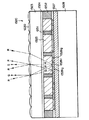
[0094]
The active matrix
[0095]
Here, looking at the G light that illuminates the
[0096]
Here, depending on the degree of modulation, the amount of light reflected by the
[0097]
At this time, the R light (polarized light) is also modulated by the operation of the liquid crystal by the electric field corresponding to the image signal formed between the
[0098]
Next, FIG. 18 is a diagram for explaining the principle of color separation and color synthesis in this example. Here, FIG. 18A is a schematic top view of the
[0099]
On the other hand, FIG. 18B corresponds to the xy section of the
[0100]
By the way, the B light for illuminating the liquid crystal panel is incident from an oblique direction of the cross section (xy plane) in the figure after being polarized by the
[0101]
Also, each B pixel electrode 1326b is arranged directly below the boundary between the microlenses, and the incident angle of the B light with respect to the liquid crystal panel is tanθ is the pixel pitch (G & B pixel) and the microlens It is preferably set to be equal to the ratio of the distance between the pixel electrodes. By the way, in the present liquid crystal panel, as described above, the RGB pixels are arranged in the order of RGRRGRG... In the z direction and BGBGBG... In the x direction. Indicates the planar arrangement. Thus, each pixel size is about half of the microlens both vertically and horizontally, and the pixel pitch is half that of the microlens in both the xz directions. In addition, the G pixel is located directly below the center of the microlens in plan view, the R pixel is located between the G pixels in the z direction and at the microlens boundary, and the B pixel is located between the G pixels in the x direction and at the microlens boundary. doing. In addition, the shape of one microlens unit is a rectangle (twice the size of a pixel).
[0102]
FIG. 19 shows a partially enlarged top view of the present liquid crystal panel. Here, a broken-
[0103]
Thus, in this liquid crystal panel, although the incident illumination positions of the primary color illumination lights are different for the RGB pixel units constituting one picture element, their emission is from the same microlens (in this case, 1322a). Done. This is also true for all other picture elements (RGB pixel units).
[0104]
Accordingly, as shown in FIG. 20, when all the emitted light from the liquid crystal panel is projected onto the
[0105]
Since the active matrix
[0106]
Incidentally, FIG. 21 shows an overall block diagram of the drive circuit system of the projection type liquid crystal display device. Here,
[0107]
FIG. 23 shows a partially enlarged top view of another form of the liquid crystal panel in the present embodiment. Here, one of the
[0108]
[Sixth Embodiment]
FIG. 24 shows a sixth embodiment of a liquid crystal panel according to the present invention. This figure is a partially enlarged sectional view of the present
[0109]
As can be seen from FIGS. 24 and 25, the
[0110]
Although the liquid crystal panel and the projection display device have been described in the fourth to sixth embodiments, a plurality of signal lines, for example, R, G, etc., are used for the drive lines of the liquid crystal pixels shown in the first to third embodiments. It is easy to obtain an accurate image and a high-quality image by matching the wiring line length and wiring capacity from the horizontal / vertical shift register to each pixel from the input analog signal line for each color. it can.
[0111]
【The invention's effect】
As described above, according to the present invention, in a liquid crystal display device having a plurality of analog video inputs, the semiconductor device has three or more analog video input lines on one side of the semiconductor device, and the analog video input lines An analog switch for transmitting an analog video signal to a desired signal line is provided between the pixel arrays, and the number of connection distances between the analog video input line and the analog switch is not adjusted in order. It was possible to provide a liquid crystal display device that can obtain high-quality image quality even when there are variations in potential.
[0112]
In the case where there are two or more analog video input lines on each side of the semiconductor device, the order of the connection distance between the analog video input line and the analog switch is different on both sides, so that there is some variation in pixel potential. Even if there was, a liquid crystal display device capable of obtaining a high quality image could be provided. In addition, even if the connection distance between the analog video input line and the analog switch is different corresponding to each of the plurality of analog video input lines, by making the length of the wiring itself equal, the pixel potential can be stably fixed, It was possible to provide a liquid crystal display device capable of precisely controlling the voltage applied to the liquid crystal and obtaining a higher quality image with the above combination.
[0113]
Furthermore, in the projection-type liquid crystal display device according to the present invention, a set of Rs constituting one picture element using an optical system or the like that illuminates each primary color light from different directions from the reflective liquid crystal panel with microlenses. Since the reflected light modulated by the liquid crystal from the G, B pixels is emitted through the same microlens, a good color image projection display with high texture without RGB mosaic becomes possible.
[0114]
Further, since the light flux from each pixel passes through the microlens twice and is substantially parallelized, a bright projection image can be obtained on the screen even if an inexpensive projection lens having a small numerical aperture is used.
[Brief description of the drawings]
FIG. 1 is a schematic circuit diagram showing a first embodiment of the present invention.
FIG. 2 is a schematic circuit diagram showing a second embodiment of the present invention.
FIG. 3 is a schematic circuit diagram used in a second embodiment of the present invention.
FIG. 4 is a schematic circuit diagram showing a third embodiment of the present invention.
FIG. 5 is a schematic circuit diagram showing a third embodiment of the present invention.
FIG. 6 is a cross-sectional view of a liquid crystal device manufactured by CMP according to the present invention.
FIG. 7 is a schematic circuit diagram of a liquid crystal device according to the present invention.
FIG. 8 is a block diagram of a liquid crystal device according to the present invention.
FIG. 9 is a circuit diagram including a delay circuit of an input unit of the liquid crystal device according to the present invention.
FIG. 10 is a conceptual diagram of a liquid crystal panel of a liquid crystal device according to the present invention.
FIG. 11 is a graph for judging whether the etching process in manufacturing the liquid crystal device according to the present invention is good or bad.
FIG. 12 is a conceptual diagram of a liquid crystal projector using a liquid crystal device according to the present invention.
FIG. 13 is a circuit block diagram showing the inside of a liquid crystal projector according to the present invention.
FIG. 14 is an overall configuration diagram showing an embodiment of an optical system of a projection type liquid crystal display device according to the present invention.
FIG. 15 is a spectral reflection characteristic diagram of a dichroic mirror used in the optical system of the projection type liquid crystal display device according to the present invention.
FIG. 16 is a perspective view of a color separation illumination unit of an optical system of a projection type liquid crystal display device according to the present invention.
FIG. 17 is a cross-sectional view of an embodiment of a liquid crystal panel according to the present invention.
FIG. 18 is a diagram illustrating the principle of color separation / color synthesis of a liquid crystal panel according to the present invention.
FIG. 19 is a partially enlarged top view of a liquid crystal panel according to an embodiment of the present invention.
FIG. 20 is a partial configuration diagram showing a projection optical system of a projection type liquid crystal display device according to the present invention.
FIG. 21 is a block diagram showing a drive circuit system of a projection type liquid crystal display device according to the present invention.
FIG. 22 is a partially enlarged view of a projected image on a screen of the projection type liquid crystal display device according to the present invention.
FIG. 23 is a partially enlarged top view of a liquid crystal panel according to an embodiment of the present invention.
FIG. 24 is a partially enlarged top view of a liquid crystal panel according to an embodiment of the present invention.
FIG. 25 is a partially enlarged top view and a sectional view of a liquid crystal panel according to an embodiment of the present invention.
FIG. 26 is a cross-sectional view showing the manufacturing process of the liquid crystal panel of the liquid crystal device.
FIG. 27 is a cross-sectional view showing the manufacturing process of the liquid crystal panel of the liquid crystal device.
FIG. 28 is a partially enlarged cross-sectional view of a transmissive liquid crystal panel with a microlens.
FIG. 29 is a partially enlarged view of a projected image on a screen of a projection liquid crystal display device using a transmissive liquid crystal panel with a microlens.
[Explanation of symbols]
1 pixel area
2 Horizontal shift register
3 Vertical shift register
41-48 analog video input line
6 Analog switch
7 Additional wiring
8 signal lines
51-54 wiring
101-103 power supply
301 Semiconductor substrate
302, 302 'p-type and n-type wells
303, 303 'source region
304 Gate area
305, 305 'drain region
306 LOCOS insulation layer
307 light shielding layer
308 PSG
309 Plasma SiN
310 Source electrode
311 Connecting electrode
312 Reflective electrode & pixel electrode
313 Antireflection film
314 Liquid crystal layer
315 Common transparent electrode
316 Counter electrode
317, 317 'high concentration impurity region
319 display area
320 Anti-reflective coating
321,322 Shift register
323 nMOS
324 pMOS
325 Retention capacity
327 Signal transfer switch
328 Reset switch
329 Reset pulse input terminal
330 Reset power supply terminal
331 Video signal input terminal
332 Boost Level Shifter
342 Inverter for pulse delay
343 switch
344 output
345 capacity
346 Protection circuit
351 Seal part
352 electrode pad
353 clock buffer
371 light source
372 condenser lens
373,375 Fresnel lens
374 Color separation optical element
376 mirror
377 Field lens
378 Liquid crystal device
379 Aperture
380 projection lens
381 screen
385 power supply
386 plug
387 Lamp temperature detection
388 Control board
389 Filter safety switch
453 main board
454 LCD panel drive headboard
455, 456, 457 Liquid crystal device
1220 micro lens (reflow heat sag type)
1251 Spacer column
1252 peripheral seal
1301 Projection lens
1302 Liquid crystal panel with micro lens
1303 Polarization beam splitter (PBS)
1306 Rod integrator
1307 Elliptical reflector
1308 Arc lamp
1309 screen
1310 Panel driver
1311 Decoder
1312 Interface circuit
1314 Ballast (Arclamp lighting circuit)
1320 Liquid Crystal Panel with Microlens
1321 Microlens glass substrate
1322 Microlens (index distribution formula)
1323 sheet glass
1324 Opposite transparent electrode
1325 liquid crystal
1326 pixel electrode
1327 Active matrix drive circuit section
1328 Silicon semiconductor substrate
1329 Basic picture element units
1340 R reflective dichroic mirror
1341 B / G Reflective Dichroic Mirror
1342 B Reflective Dichroic Mirror
1343 High reflection mirror
1350 Fresnel lens (second condenser lens)
1351 First condenser lens
Claims (1)
前記液晶パネルは、液晶画素及び該液晶画素を駆動するためのスイッチングトランジスタを水平方向及び垂直方向からなるマトリクス形状で配置し、該水平方向のスイッチングトランジスタをゲート線で共通接続し、該垂直方向のスイッチングトランジスタを垂直配線で共通接続し、水平方向のスイッチングトランジスタをオン状態にする電位をゲート線に印加して、行を選択し、該行上のスイッチングトランジスタに接続した液晶画素を駆動するアクテイブマトリクス回路を有し、
前記3本以上のアナログビデオ信号線は、各々1本毎に、アナログスイッチを介して、前記垂直配線に接続され、
前記選択された行上のスイッチングトランジスタを接続している垂直配線上の前記アナログスイッチと前記アナログビデオ入力線との間の垂直配線の接続距離は、前記選択された行上の水平方向で隣合う液晶画素において、該接続距離の大小がソートされていない、ことを特徴とする液晶表示装置。 A liquid crystal display device that divides an analog video signal into three or more analog video signal lines and applies it to a liquid crystal panel,
In the liquid crystal panel, liquid crystal pixels and switching transistors for driving the liquid crystal pixels are arranged in a matrix shape composed of a horizontal direction and a vertical direction, the horizontal direction switching transistors are connected in common by a gate line, and the vertical direction An active matrix for driving a liquid crystal pixel connected to a switching transistor on a row by connecting a switching transistor in common with a vertical wiring, applying a potential for turning on a horizontal switching transistor to a gate line, selecting a row Have a circuit,
Each of the three or more analog video signal lines is connected to the vertical wiring via an analog switch for each one.
The vertical wiring connection distance between the analog switch on the vertical wiring connecting the switching transistors on the selected row and the analog video input line is adjacent in the horizontal direction on the selected row. in the liquid crystal pixel, the magnitude of the connection distance is not sorted, a liquid crystal display device, characterized in that.
Priority Applications (1)
| Application Number | Priority Date | Filing Date | Title |
|---|---|---|---|
| JP29247097A JP3630945B2 (en) | 1997-10-24 | 1997-10-24 | Liquid crystal display |
Applications Claiming Priority (1)
| Application Number | Priority Date | Filing Date | Title |
|---|---|---|---|
| JP29247097A JP3630945B2 (en) | 1997-10-24 | 1997-10-24 | Liquid crystal display |
Publications (2)
| Publication Number | Publication Date |
|---|---|
| JPH11125805A JPH11125805A (en) | 1999-05-11 |
| JP3630945B2 true JP3630945B2 (en) | 2005-03-23 |
Family
ID=17782237
Family Applications (1)
| Application Number | Title | Priority Date | Filing Date |
|---|---|---|---|
| JP29247097A Expired - Fee Related JP3630945B2 (en) | 1997-10-24 | 1997-10-24 | Liquid crystal display |
Country Status (1)
| Country | Link |
|---|---|
| JP (1) | JP3630945B2 (en) |
Families Citing this family (2)
| Publication number | Priority date | Publication date | Assignee | Title |
|---|---|---|---|---|
| TW567363B (en) | 1999-05-14 | 2003-12-21 | Seiko Epson Corp | Method for driving electrooptical device, drive circuit, electrooptical device, and electronic device |
| GB0014074D0 (en) * | 2000-06-10 | 2000-08-02 | Koninkl Philips Electronics Nv | Active matrix array devices |
-
1997
- 1997-10-24 JP JP29247097A patent/JP3630945B2/en not_active Expired - Fee Related
Also Published As
| Publication number | Publication date |
|---|---|
| JPH11125805A (en) | 1999-05-11 |
Similar Documents
| Publication | Publication Date | Title |
|---|---|---|
| JP3445121B2 (en) | Matrix substrate, liquid crystal display device and projector using the same | |
| JP3571887B2 (en) | Active matrix substrate and liquid crystal device | |
| JP3188411B2 (en) | Pixel electrode substrate for reflective liquid crystal device, liquid crystal device using the pixel electrode substrate, and display device using the liquid crystal device | |
| US6127998A (en) | Matrix substrate, liquid-crystal device incorporating the matrix substrate, and display device incorporating the liquid-crystal device | |
| KR100325924B1 (en) | Matrix substrates, liquid crystal devices using this matrix substrate, and display devices using this liquid crystal device | |
| JP3249077B2 (en) | Matrix substrate and liquid crystal device | |
| US6809790B2 (en) | Matrix substrate, liquid crystal display device using it, and method for producing the matrix substrate | |
| JPH10254370A (en) | Display panel and projection type display device using it | |
| JP3249079B2 (en) | Matrix substrate, liquid crystal display and projection type liquid crystal display | |
| JP3279234B2 (en) | Method for manufacturing semiconductor device | |
| JPH11125834A (en) | Matrix substrate and liquid crystal display device and projection type liquid crystal display device | |
| JPH11126051A (en) | Matrix substrate and liquid crystal display device, and projection type liquid crystal display device using them | |
| JP3630945B2 (en) | Liquid crystal display | |
| JPH11133457A (en) | Matrix substrate, display device, its manufacture and projection liquid crystal display device | |
| JP3230659B2 (en) | Semiconductor device, display device substrate, liquid crystal device using the display device substrate, projection type liquid crystal display device, and display device | |
| JP3199311B2 (en) | Display device substrate, liquid crystal device using the substrate, display device, projection type liquid crystal display device, and method for manufacturing display device substrate | |
| JP3423592B2 (en) | Display substrate, method of manufacturing the same, liquid crystal display device, and projection type liquid crystal display device | |
| JP3423593B2 (en) | Liquid crystal display device, manufacturing method thereof, display device substrate, and projection type liquid crystal display device | |
| JPH11126035A (en) | Display device, liquid crystal display device and liquid crystal projector using the same | |
| JP2001147426A (en) | Pixel electrode substrate and reflection type liquid crystal device using the same | |
| JP2000180884A (en) | Liquid crystal display device | |
| JPH11135497A (en) | Layer insulation film and manufacture of display device | |
| JP2000330124A (en) | Production of electrode substrate and liquid crystal device | |
| JPH11133456A (en) | Matrix substrate, liquid crystal display device, display device and liquid crystal projector device using the same | |
| JPH11135502A (en) | Wiring for semiconductor device, semiconductor device therewith, and manufacture thereof |
Legal Events
| Date | Code | Title | Description |
|---|---|---|---|
| A977 | Report on retrieval |
Free format text: JAPANESE INTERMEDIATE CODE: A971007 Effective date: 20040331 |
|
| A131 | Notification of reasons for refusal |
Free format text: JAPANESE INTERMEDIATE CODE: A131 Effective date: 20040805 |
|
| A521 | Written amendment |
Free format text: JAPANESE INTERMEDIATE CODE: A523 Effective date: 20040901 |
|
| TRDD | Decision of grant or rejection written | ||
| A01 | Written decision to grant a patent or to grant a registration (utility model) |
Free format text: JAPANESE INTERMEDIATE CODE: A01 Effective date: 20041207 |
|
| A61 | First payment of annual fees (during grant procedure) |
Free format text: JAPANESE INTERMEDIATE CODE: A61 Effective date: 20041215 |
|
| R150 | Certificate of patent or registration of utility model |
Free format text: JAPANESE INTERMEDIATE CODE: R150 |
|
| FPAY | Renewal fee payment (event date is renewal date of database) |
Free format text: PAYMENT UNTIL: 20081224 Year of fee payment: 4 |
|
| FPAY | Renewal fee payment (event date is renewal date of database) |
Free format text: PAYMENT UNTIL: 20081224 Year of fee payment: 4 |
|
| FPAY | Renewal fee payment (event date is renewal date of database) |
Free format text: PAYMENT UNTIL: 20091224 Year of fee payment: 5 |
|
| FPAY | Renewal fee payment (event date is renewal date of database) |
Free format text: PAYMENT UNTIL: 20091224 Year of fee payment: 5 |
|
| FPAY | Renewal fee payment (event date is renewal date of database) |
Free format text: PAYMENT UNTIL: 20101224 Year of fee payment: 6 |
|
| FPAY | Renewal fee payment (event date is renewal date of database) |
Free format text: PAYMENT UNTIL: 20111224 Year of fee payment: 7 |
|
| LAPS | Cancellation because of no payment of annual fees |