JP3626933B2 - Manufacturing method of substrate mounting table - Google Patents
Manufacturing method of substrate mounting table Download PDFInfo
- Publication number
- JP3626933B2 JP3626933B2 JP2001393918A JP2001393918A JP3626933B2 JP 3626933 B2 JP3626933 B2 JP 3626933B2 JP 2001393918 A JP2001393918 A JP 2001393918A JP 2001393918 A JP2001393918 A JP 2001393918A JP 3626933 B2 JP3626933 B2 JP 3626933B2
- Authority
- JP
- Japan
- Prior art keywords
- substrate
- dielectric material
- material film
- susceptor
- mounting table
- Prior art date
- Legal status (The legal status is an assumption and is not a legal conclusion. Google has not performed a legal analysis and makes no representation as to the accuracy of the status listed.)
- Expired - Lifetime
Links
Images


Classifications
-
- G—PHYSICS
- G02—OPTICS
- G02F—OPTICAL DEVICES OR ARRANGEMENTS FOR THE CONTROL OF LIGHT BY MODIFICATION OF THE OPTICAL PROPERTIES OF THE MEDIA OF THE ELEMENTS INVOLVED THEREIN; NON-LINEAR OPTICS; FREQUENCY-CHANGING OF LIGHT; OPTICAL LOGIC ELEMENTS; OPTICAL ANALOGUE/DIGITAL CONVERTERS
- G02F1/00—Devices or arrangements for the control of the intensity, colour, phase, polarisation or direction of light arriving from an independent light source, e.g. switching, gating or modulating; Non-linear optics
- G02F1/01—Devices or arrangements for the control of the intensity, colour, phase, polarisation or direction of light arriving from an independent light source, e.g. switching, gating or modulating; Non-linear optics for the control of the intensity, phase, polarisation or colour
- G02F1/13—Devices or arrangements for the control of the intensity, colour, phase, polarisation or direction of light arriving from an independent light source, e.g. switching, gating or modulating; Non-linear optics for the control of the intensity, phase, polarisation or colour based on liquid crystals, e.g. single liquid crystal display cells
-
- H—ELECTRICITY
- H01—ELECTRIC ELEMENTS
- H01J—ELECTRIC DISCHARGE TUBES OR DISCHARGE LAMPS
- H01J37/00—Discharge tubes with provision for introducing objects or material to be exposed to the discharge, e.g. for the purpose of examination or processing thereof
- H01J37/32—Gas-filled discharge tubes
- H01J37/32009—Arrangements for generation of plasma specially adapted for examination or treatment of objects, e.g. plasma sources
- H01J37/32082—Radio frequency generated discharge
-
- C—CHEMISTRY; METALLURGY
- C23—COATING METALLIC MATERIAL; COATING MATERIAL WITH METALLIC MATERIAL; CHEMICAL SURFACE TREATMENT; DIFFUSION TREATMENT OF METALLIC MATERIAL; COATING BY VACUUM EVAPORATION, BY SPUTTERING, BY ION IMPLANTATION OR BY CHEMICAL VAPOUR DEPOSITION, IN GENERAL; INHIBITING CORROSION OF METALLIC MATERIAL OR INCRUSTATION IN GENERAL
- C23C—COATING METALLIC MATERIAL; COATING MATERIAL WITH METALLIC MATERIAL; SURFACE TREATMENT OF METALLIC MATERIAL BY DIFFUSION INTO THE SURFACE, BY CHEMICAL CONVERSION OR SUBSTITUTION; COATING BY VACUUM EVAPORATION, BY SPUTTERING, BY ION IMPLANTATION OR BY CHEMICAL VAPOUR DEPOSITION, IN GENERAL
- C23C16/00—Chemical coating by decomposition of gaseous compounds, without leaving reaction products of surface material in the coating, i.e. chemical vapour deposition [CVD] processes
- C23C16/44—Chemical coating by decomposition of gaseous compounds, without leaving reaction products of surface material in the coating, i.e. chemical vapour deposition [CVD] processes characterised by the method of coating
- C23C16/458—Chemical coating by decomposition of gaseous compounds, without leaving reaction products of surface material in the coating, i.e. chemical vapour deposition [CVD] processes characterised by the method of coating characterised by the method used for supporting substrates in the reaction chamber
- C23C16/4581—Chemical coating by decomposition of gaseous compounds, without leaving reaction products of surface material in the coating, i.e. chemical vapour deposition [CVD] processes characterised by the method of coating characterised by the method used for supporting substrates in the reaction chamber characterised by material of construction or surface finish of the means for supporting the substrate
-
- H—ELECTRICITY
- H01—ELECTRIC ELEMENTS
- H01J—ELECTRIC DISCHARGE TUBES OR DISCHARGE LAMPS
- H01J2237/00—Discharge tubes exposing object to beam, e.g. for analysis treatment, etching, imaging
- H01J2237/02—Details
- H01J2237/022—Avoiding or removing foreign or contaminating particles, debris or deposits on sample or tube
-
- Y—GENERAL TAGGING OF NEW TECHNOLOGICAL DEVELOPMENTS; GENERAL TAGGING OF CROSS-SECTIONAL TECHNOLOGIES SPANNING OVER SEVERAL SECTIONS OF THE IPC; TECHNICAL SUBJECTS COVERED BY FORMER USPC CROSS-REFERENCE ART COLLECTIONS [XRACs] AND DIGESTS
- Y10—TECHNICAL SUBJECTS COVERED BY FORMER USPC
- Y10T—TECHNICAL SUBJECTS COVERED BY FORMER US CLASSIFICATION
- Y10T279/00—Chucks or sockets
- Y10T279/23—Chucks or sockets with magnetic or electrostatic means
Landscapes
- Chemical & Material Sciences (AREA)
- Physics & Mathematics (AREA)
- Engineering & Computer Science (AREA)
- Materials Engineering (AREA)
- Analytical Chemistry (AREA)
- Mechanical Engineering (AREA)
- Metallurgy (AREA)
- Organic Chemistry (AREA)
- General Chemical & Material Sciences (AREA)
- Plasma & Fusion (AREA)
- Chemical Kinetics & Catalysis (AREA)
- Nonlinear Science (AREA)
- Crystallography & Structural Chemistry (AREA)
- General Physics & Mathematics (AREA)
- Optics & Photonics (AREA)
- Container, Conveyance, Adherence, Positioning, Of Wafer (AREA)
- Drying Of Semiconductors (AREA)
Description
【0001】
【発明が属する技術分野】
本発明は、液晶表示装置(LCD)用のガラス基板等の基板を載置する基板載置台の製造方法に関する。
【0002】
【従来の技術】
例えば、LCD製造プロセスにおいては、被処理基板であるガラス製のLCD基板に対して、ドライエッチングやスパッタリング、CVD(化学気相成長)等のプラズマ処理が多用されている。
【0003】
このようなプラズマ処理においては、例えば、チャンバー内に一対の平行平板電極(上部および下部電極)を配置し、下部電極として機能するサセプタ(載置台)に被処理基板を載置し、処理ガスをチャンバー内に導入するとともに、電極の少なくとも一方に高周波を印加して電極間に高周波電界を形成し、この高周波電界により処理ガスのプラズマを形成して被処理基板に対してプラズマ処理を施す。この際、被処理基板はサセプタ表面に面接触するようになっている。
【0004】
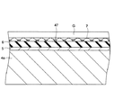
ところが、サセプタの表面は、実際には緩曲面となっているため、基板とサセプタとの間には部分的に微少な隙間ができている。一方、プラズマ処理を繰り返し行うことによりサセプタ上に付着物が蓄積する。
この際、図8に示すように、付着物47は被処理基板Gとサセプタ50との隙間を埋めるように蓄積する。このため、被処理基板G裏面にサセプタ50が接触する部分と付着物47が接触する部分とができて、これらの部分間で熱伝導性や導電性が異なってしまい、被処理基板Gにエッチングむら(被処理基板Gにおいてエッチングレートの高い部分と低い部分とが混在することをいう)が生じることがある。また、このような付着物47の存在によりサセプタ50に載置された被処理基板Gがサセプタ50に吸着されてしまうこともある。
【0005】
そのため、たとえば、特開昭59−172237号公報に開示されたプラズマ処理装置においては、サセプタ(試料ステージ)に複数のたとえば円錐状の突起部を設けている。しかし、この公報の第2図によれば、ステージ22と突起物23は一体物になっている。金属の機械加工により、このような均一な突起物を作成することは、技術的に困難であり、コスト・時間もかかる。
【0006】
また、特開昭60−261377号公報に開示された静電チャックおよびその製造方法においては、静電電極を覆う焼成セラミック絶縁層の表面に凸状パターンが形成されている。
【0007】
また、特開平8−70034号公報に開示された静電力低減のためのパターン付きサセプタにおいては、サセプタ表面にフォトエッチングにより凹凸パターンを形成して、静電力(固着力)を低減し、プラズマ処理後にサセプタからウエハを容易に分離できるようにしている。
【0008】
また、特開平10−340896号公報に開示されたプラズマCVD装置用サセプタおよびその製造方法においては、アルミニウム又はアルミニウム合金製のサセプタの表面をショットブラスト処理して凹凸部を形成し、さらに化学研磨、電解研磨、又はバフ研磨によって凸部の急峻な突起部を除去している。
【0009】
しかし、これら従来技術はいずれも凸部の頂上は平らであるため、プラズマ処理によって発生した埃が堆積しやすいという欠点がある。
【0010】
【発明が解決しようとする課題】
そこで、本発明は、基板載置台の表面に付着物が蓄積することによって生じるエッチングむら等の処理むらを防止し、基板が基板載置台に吸着されてしまうこと等の不都合が生じ難い基板載置台の製造方法を提供することを課題としている。
【0011】
【課題を解決するための手段】
上記の課題を解決するため、本発明の第1の観点では、基板に処理を施す際に基板を載置する基板載置台の製造方法であって、基材表面に誘電性材料膜を形成する工程と、前記誘電性材料膜の上に、複数の開口を有する開口板を、前記開口板の開口部以外の面積より小さい面積を有するとともに前記開口板の開口に対応する部分に存在しない中間部材を介して前記誘電性材料膜から浮かせた状態で設け、前記開口板を介してセラミックスを溶射してセラミックスからなる複数の凸部を形成する工程とを含むことを特徴とする基板載置台の製造方法を提供する。
【0012】
本発明の第2の観点では、基板に処理を施す際に基板を載置する基板載置台の製造方法であって、基材上に第1の誘電性材料膜を形成する工程と、前記第1の誘電性材料膜上に導電層を形成する工程と、前記導電層上に第2の誘電性材料膜を形成する工程と、前記第2の誘電性材料膜上に、複数の開口を有する開口板を、前記開口板の開口部以外の面積より小さい面積を有するとともに前記開口板の開口に対応する部分に存在しない中間部材を介して前記第2の誘電性材料膜から浮かせた状態で設け、前記開口板を介してセラミックスを溶射してセラミックスからなる複数の凸部を形成する工程とを含むことを特徴とする基板載置台の製造方法を提供する。
【0018】
以上のような構成によれば、誘電性材料膜の上にセラミックスからなる凸部を形成するので、これら凸部がスペーサーの役割をはたし、基板載置台上に付着物が蓄積しても付着物が被処理基板に接触し難くなる。また、凸部を溶射で形成することにより、基板載置台において、セラミックスからなる複数の凸部を容易にかつ一様に分布させることができ、このような効果が高まる。そして、溶射により凸部を形成する際に、誘電性材料膜の上に、複数の開口を有する開口板を、前記開口板の開口部以外の面積より小さい面積を有するとともに前記開口板の開口に対応する部分に存在しない中間部材を介して前記誘電性材料膜から浮かせた状態で設け、前記開口板を介してセラミックスを溶射してセラミックスからなる凸部を形成することにより、凸部を、上部が曲面のみからなり、一様に分布したものとすることが可能となる。このように、凸部の上部が曲面のみからなるものとすることで基板と点接触させることができ、付着物が付着しにくくなるとともに、凸部に尖った箇所が存在しない状態となるので突起が削れてパーティクルの原因となることがない。したがって、被処理基板裏面に基板載置台が接触する部分と付着物が接触する部分とができることに起因したエッチングむらや、被処理基板が基板載置台に吸着されること等の不都合が生じることを防止することができる。また、表面に、その外縁に沿って、上記凸部の高さ以上の高さを有する台部を設けたので、基板裏面に熱伝導媒体を供給した場合に、熱伝導媒体が基板載置台以外の領域に拡散することを抑制することができる。そして、さらに凸部の高さを50〜100μmとすることにより、凸部の強度や処理効率を低下させずに付着物による悪影響を十分に防止することができ、上記効果を一層高めることができる。
【0019】
【発明の実施の形態】
以下、添付図面を参照して本発明の実施の形態について説明する。
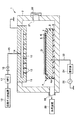
図1は、本発明の一実施形態に係る基板載置台としてのサセプタが設けられた処理装置の一例であるプラズマエッチング装置を示す断面図である。図1に示すように、本発明の一実施形態の基板載置台であるサセプタ4は、基材4aと、基材4aの上に設けられた誘電性材料膜6と、誘電性材料膜6の上に設けられた凸部7とを有する。
【0020】
凸部7は、誘電体材料膜6の上の基板G載置領域に一様に分布して形成されており、基板Gはこの凸部7上に載置されるようになっている。これにより凸部7はサセプタ4と基板Gとの間を離隔するスペーサーとして機能し、サセプタ4上に付着した付着物が基板Gに悪影響を及ぼすことが防止される。この凸部7は、その高さが50〜100μmであることが好ましい。サセプタ4上に付着する付着物の量を考慮すると、凸部7の高さを50μm以上とすることで付着物が基板Gに悪影響を及ぼすことを十分に防止することができるからである。一方、高さが100μmを超えると凸部7の強度が低下したり、基板Gのエッチングレートが低下するといった問題や、後述するように凸部7を溶射で形成する場合に溶射時間が長くなるという不都合もある。また、凸部7の径は0.5〜1mmであることが好ましく、その間隔は0.5〜30mmとすること、さらには5〜10mmとすることが好ましい。配列パターンには特に制限はなく、例えば千鳥格子配列であってもよい。
【0021】
凸部7は、少なくともその上部を曲面形状や半球状に形成して、基板Gと点接触させることが好ましい。これにより、凸部7と基板Gとの接触部分に付着物が極めて付着し難くすることができる。一方、凸部7の形状を円柱または角柱とした場合には、上面が平面であり、この上面に付着物が付着しやすくなる欠点がある。
【0022】
凸部7は一般的に耐久性および耐食性が高い材料として知られているセラミックスで構成されている。凸部7を構成するセラミックスは特に限定されるものではなく、典型的にはAl2O3、Zr2O3、Si3N4等の絶縁材料を挙げることができるが、SiCのようにある程度導電性を有するものであってもよい。凸部7は溶射により形成される。
【0023】
誘電性材料膜6は、誘電性材料からなっていればその材料は問わず、また高絶縁性材料のみならず電荷の移動を許容する程度の導電性を有するものを含む。このような誘電性材料膜6は、耐久性および耐食性の観点からセラミックスで構成することが好ましい。この際のセラミックスは特に限定されるものではなく、凸部7の場合と同様、典型的にはAl2O3、Zr2O3、Si3N4等の絶縁材料を挙げることができるが、SiCのようにある程度導電性を有するものであってもよい。このような誘電体材料膜6は溶射により形成してもよい。また、溶射した後、研磨用によって表面を平滑化してもよい。
【0024】
基材4aは、誘電体材料膜6を支持するものであり、例えばアルミニウム等の金属やカーボンのような導電体で構成されている。
【0025】
次に、誘電性材料膜6上に凸部7を溶射によって形成する方法について説明する。
凸部7は機械加工やエッチング等の他の方法でも形成することも考えられるが、この場合には技術的、コスト的に問題がある。そこで、本実施形態では以下のような方法を採用する。
【0026】
図2に示すように、まず、複数の円形開口を有する開口板66を誘電性材料膜6上に非接触に位置させる。そのためには、中間部材65を誘電性材料膜6上に載せ、さらにその上に開口板66を載せる。すなわち、開口板66と誘電性材料膜6との間に中間部材65を置き、開口板66を浮かせる。中間部材65の材料は金属または耐熱性の樹脂等が好適である。また、接着層付耐熱性樹脂シートであれば誘電性材料膜6に接着することができて好都合である。中間部材65は、開口板66の開口部以外の面積より小さい面積を有するとともに開口板66の開口に対応する部分に存在しない。開口板66は、たとえば、板厚0.3mm程度の金属板、具体的にはステンレス板を使用する。この開口板66を介して溶射し、開口に対応する部分に凸部7を形成する。これにより、比較的容易に凸部7を形成することができる。また、このように複数の開口を有するマスク部材を介して溶射することにより、凸部7の上部の形状を曲面形状にすることができる。これは、溶射の際に開口の周辺部が障壁となりセラミックスの拡散が妨げられるためと考えられる。
【0027】
このようにすることにより、溶射によって形成される凸部を所望の形状に制御することができる。溶射後は、開口板66および中間部材65は取りはずす。
【0028】
また、凸部7をセラミックスの溶射で形成する際に、気孔が形成される場合があるが、その場合には凸部7を形成した後に封孔処理を施す。誘電性材料膜6を溶射により形成する際も同様である。
【0029】
また、誘電性材料膜6の材質と凸部7の材質が同一であれば、両者は強固に結合するので好適である。しかし、処理中の温度範囲で両者の結合が十分であれば、両者の材質は異なっていてもよい。なお、凸部7および誘電性材料膜6を同一の材料で構成する場合には、これらを溶射により連続して形成することができる。
【0030】
また、基材4aと誘電性材料膜6の間に層5が設けられている。層5は、熱膨張係数が基材4aと誘電性材料膜6との中間の値を示す材料からなり、基材4aと誘電性材料膜6との熱膨張差を緩和する機能を有している。また、基材4aと誘電性材料膜6との接合を強化するために設けてもよい。なお、層5は必須なものではなく、サセプタ4のサイズが小さい場合や温度の変化量が小さい場合や基材4aと誘電性材料膜6との接合が強固な場合には層5を省いてもよい。また、層5は1つに限らず2つ以上設けてもよい。
【0031】
この層5は、基材4aをアルミニウムで構成し、誘電性材料膜6をセラミックスで構成する場合には、例えばニッケルおよびアルミニウムの合金で構成することができる。なお、層5の形成方法は問わない。
【0032】
サセプタ4においては、エッチングプロセスを繰り返すことにより、図3に示すように、基材4a上に形成された誘電性材料膜6の表面には基板Gからエッチングされた物質等の付着物47が蓄積するが、本実施形態においては、凸部7がスペーサーの役割をはたし、サセプタ4上に付着物が蓄積しても付着物が基板Gに接触し難く、これにより基板Gにサセプタ4と接触する部分および付着物47と接触する部分ができてエッチングむらが生じたり、基板Gがサセプタ4に吸着されるといった不都合が防止される。
【0033】
次に、再び図1を参照して、上述した構成のサセプタ4を用いた本発明の処理装置について説明する。この処理装置1は、LCDガラス基板の所定の処理を行う装置の断面図であり、容量結合型平行平板プラズマエッチング装置を例として構成されている。ただし、本発明の処理装置はプラズマエッチング装置にのみ限定されるものではない。
【0034】
このプラズマエッチング装置1は、例えば表面がアルマイト処理(陽極酸化処理)されたアルミニウムからなる角筒形状に成形されたチャンバー2を有している。このチャンバー2内の底部には絶縁材からなる角柱状の絶縁板3が設けられており、さらにこの絶縁板3の上には、被処理基板であるLCDガラス基板Gを載置するための前述したサセプタ4が設けられている。また、サセプタ4の基材4aの外周および上面の層5および誘電性材料膜6が設けられていない周縁には、絶縁部材8が設けられている。
【0035】
サセプタ4には、高周波電力を供給するための給電線23が接続されており、この給電線23には整合器24および高周波電源25が接続されている。高周波電源25からは例えば13.56MHzの高周波電力がサセプタ4に供給される。
【0036】
前記サセプタ4の上方には、このサセプタ4と平行に対向して上部電極として機能するシャワーヘッド11が設けられている。シャワーヘッド11はチャンバー2の上部に支持されており、内部に内部空間12を有するとともに、サセプタ4との対向面に処理ガスを吐出する複数の吐出孔13が形成されている。このシャワーヘッド11は接地されており、サセプタ4とともに一対の平行平板電極を構成している。
【0037】
シャワーヘッド11の上面にはガス導入口14が設けられ、このガス導入口14には、処理ガス供給管15が接続されており、この処理ガス供給管15には、バルブ16、およびマスフローコントローラ17を介して、処理ガス供給源18が接続されている。処理ガス供給源18からは、エッチングのための処理ガスが供給される。処理ガスとしては、ハロゲン系のガス、O2ガス、Arガス等、通常この分野で用いられるガスを用いることができる。
【0038】
前記チャンバー2の側壁底部には排気管19が接続されており、この排気管19には排気装置20が接続されている。排気装置20はターボ分子ポンプなどの真空ポンプを備えており、これによりチャンバー2内を所定の減圧雰囲気まで真空引き可能なように構成されている。また、チャンバー2の側壁には基板搬入出口21と、この基板搬入出口21を開閉するゲートバルブ22とが設けられており、このゲートバルブ22を開にした状態で基板Gが隣接するロードロック室(図示せず)との間で搬送されるようになっている。
【0039】
次に、このように構成されるプラズマエッチング装置1における処理動作について説明する。
まず、被処理体である基板Gは、ゲートバルブ22が開放された後、図示しないロードロック室から基板搬入出口21を介してチャンバー2内へと搬入され、サセプタ4上に形成された誘電性材料膜6の凸部7上に載置される。この場合に、基板Gの受け渡しはサセプタ4の内部を挿通しサセプタ4から突出可能に設けられたリフターピン(図示せず)を介して行われる。その後、ゲートバルブ22が閉じられ、排気装置20によって、チャンバー2内が所定の真空度まで真空引きされる。
【0040】
その後、バルブ16が開放されて、処理ガス供給源18から処理ガスがマスフローコントローラ17によってその流量が調整されつつ、処理ガス供給管15、ガス導入口14を通ってシャワーヘッド11の内部空間12へ導入され、さらに吐出孔13を通って基板Gに対して均一に吐出され、チャンバー2内の圧力が所定の値に維持される。
【0041】
この状態で高周波電源25から整合器24を介して高周波電力がサセプタ4に印加され、これにより、下部電極としてのサセプタ4と上部電極としてのシャワーヘッド11との間に高周波電界が生じ、処理ガスが解離してプラズマ化し、これにより基板Gにエッチング処理が施される。
【0042】
このようにしてエッチング処理を施した後、高周波電源25からの高周波電力の印加を停止し、チャンバー2内の圧力が所定の圧力まで昇圧され、ゲートバルブ22が開放され、基板Gが基板搬入出口21を介してチャンバー2内から図示しないロードロック室へ搬出されることにより基板Gのエッチング処理は終了する。
【0043】
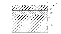
上述したサセプタ(基板載置台)4には静電チャックを設けてもよい。この場合には、図4に示すように、サセプタの基材4a上に第1の誘電性材料膜31、静電電極層として機能する導電層32、第2の誘電性材料膜6′、凸部7′をこの順に積層してサセプタ4′を構成すればよい。
【0044】
静電チャック部の第1の誘電性材料膜31、導電層32、第2の誘電性材料膜6′を形成する方法は問わないが、すべて溶射によって形成してもよい。また、一部または全部の層を研磨等により平滑化してもよい。
【0045】
凸部7′は上述の凸部7と同様、セラミックスで構成されており、そのセラミックスは特に限定されるものではなく、典型的にはAl2O3、Zr2O3、Si3N4等の絶縁材料を挙げることができるが、SiCのようにある程度導電性を有するものであってもよい。第1の誘電性材料膜31と第2の誘電性材料膜6′は、上記誘電性材料膜6と同様、誘電性材料からなっていればその材料は問わず、また高絶縁材料のみならず電荷の移動を許容する程度の導電性を有するものを含み、耐久性および耐食性の観点からセラミックスで構成することが好ましい。この際のセラミックスは特に限定されるものではなく、典型的にはAl2O3、Zr2O3、Si3N4等の絶縁材料を挙げることができるが、SiCのようにある程度導電性を有するものであってもよい。また、第1の誘電性材料膜31と第2の誘電性材料膜6′は同じ材質であってもよい。また、基材4aと第1の誘電性材料膜31との間や第2の誘電性材料膜6′と凸部7′との間に1以上の中間層を設けることもできる。この中間層の機能は、前記層5と同様である。
【0046】
凸部7′は第2の誘電性材料膜6′の基板G載置領域に一様に分布しており、基板Gはこの凸部7′上に吸着されるようになっている。この第2の誘電性材料膜6′と凸部7′の形状およびその形成方法は、上記誘電性材料膜6および凸部7について既に説明したものと同様である。なお、このような構造をとらなくても、図1に示すサセプタ4の基材4aを静電チャックの静電電極とすることにより静電チャックとして機能させることができる。
【0047】
このように、静電チャックにより基板Gを静電吸着するとともに、温調しながら、基板Gの処理、例えばエッチング処理を行う。そしてエッチング処理を繰り返すことにより、静電チャック上に形成された表層部6表面に付着物が蓄積するが、本実施形態においても、凸部7′がスペーサーの役割をはたすため、付着物が基板Gに接触し難い。したがって、基板Gにサセプタと接触する部分および付着物と接触する部分ができてエッチングむらが生じたり、静電チャックによる静電吸着を解除した後も基板Gがサセプタに固着されるといった不都合が防止される。
【0048】
次に、他の実施形態について説明する。
図5の(a)、(b)に示すサセプタ100は、 基材4aと、前記基材4a上に形成した層5と、前記層5上に形成した誘電性材料膜6と、誘電性材料膜6上の凸部7とを備えており、基材4aを貫通して、基材4aの表面の周縁部に吹出口を有する複数の伝熱媒体流路99が形成されている。これによって、凸部間の空間に熱伝導媒体たとえばヘリウムガスを充満させて基板を一様に冷却することができ、基板の温度を一様にすることができるので、エッチング等のプラズマ処理も基板前面にわたって一様となる。また、エッジ付近に台部101が設けられており、この台部101によって、熱伝導媒体がサセプタ以外の領域に拡散することを抑制することができる。この台部101の表面の高さは、前記凸部7の高さ以上である。
【0049】
図6の(a)、(b)に示すサセプタ100′は、台部101に溝部102を設け、この溝部102に伝熱媒体流路99の吹出口が設けられているものである。この溝部102によっても、熱伝導媒体がサセプタ以外の領域に拡散することを抑制することができる。
【0050】
なお、図5および図6のサセプタにおいても、上述したように静電チャックを設けることができる。
【0051】
図7に示すサセプタ100″は、図示するように平面形状が矩形状であり、複数の凸部7は直交格子を構成し、前記直交格子のひとつの軸Yが前記矩形のひとつの辺Xとなす角度θが0°を超え45°以下としてある。ここにいう直交格子とは、単位格子(基本格子)が矩形であるような格子である。ガラス基板等の矩形の基板には、半導体回路パターンが露光され、エッチングによってその半導体回路パターン等が現像される。この半導体回路パターン等においては、矩形の各辺に平行にソースライン、ゲートラインその他が配列されているため、サセプタの各凸部が特定のパターンと重なると、その凸部で基板との接触の異常のため、熱伝導や電界が変動し、エッチングむらを生じる虞がある。このサセプタ100″は、このようなエッチングむらを抑制するためのものである。また、このようにエッチングむらを抑制する観点からは、このような直交格子ではなく、凸部7が不規則に配置されているものであってもよい。このようなエッチングむらを抑制するサセプタに図5または図6の構成を採用することもできる。
【0052】
以上のヘリウムガス等の伝熱媒体を吹き出すための伝熱媒体流路99を有する図5から図7のサセプタを備えた処理装置は、基材4aを貫通してヘリウム等の伝熱媒体流路99は例えばヘリウム源に接続されている以外の点は図1に示した処理装置と同様である。
【0053】
なお、本発明は以上説明した実施形態に限定されるものではない。例えば、本発明の処理装置については、下部電極に高周波電力を印加するRIEタイプの容量結合型平行平板プラズマエッチング装置を例示して説明したが、エッチング装置に限らず、アッシング、CVD成膜等の他のプラズマ処理装置に適用することができるし、上部電極に高周波電力を供給するタイプであっても、また容量結合型に限らず誘導結合型であってもよい。また、被処理基板はLCDガラス基板Gに限られず半導体ウエハであってもよい。
【0054】
【発明の効果】
以上説明したように、本発明によれば、誘電性材料膜の上に、複数の開口を有する開口板を載置し、開口板を介してセラミックスを溶射して凸部を形成するので、基板載置台において、セラミックスからなる複数の凸部を容易にかつ一様に分布させることができ、これら凸部がスペーサーの役割をはたし、前記載置台上に付着物が蓄積しても付着物が被処理基板に接触し難くなる。したがって、被処理基板裏面に前記載置台が接触する部分と付着物が接触する部分とができることに起因したエッチングむらや、被処理基板が前記載置台に吸着されること等の不都合が生じることを防止することができる。
【図面の簡単な説明】
【図1】本発明の一実施形態に係る基板載置台としてのサセプタが設けられた処理装置の一例であるプラズマエッチング装置を示す断面図。
【図2】図1の装置に設けられたサセプタの凸部の形成方法を説明するための断面図。
【図3】本発明のサセプタ(基板載置台)に付着物が付着した状態を示す断面図。
【図4】静電チャックを設けた他の実施形態に係るサセプタを示す断面図。
【図5】さらに他の実施形態に係るサセプタを示す断面図および部分平面図
【図6】別の実施形態に係るサセプタを示す断面図および部分平面図
【図7】また別の実施形態に係るサセプタを示す平面図
【図8】従来のサセプタ上に付着物が付着した状態を示す断面図
【符号の説明】
1 処理装置(プラズマエッチング装置)
2 チャンバー(処理室)
3 絶縁板
4,100,100′,100″ サセプタ
5 層
6 誘電性材料膜
6′ 第2の誘電性材料膜
7,7′ 凸部
11 シャワーヘッド(ガス供給手段)
20 排気装置
31 第1の誘電性材料膜
32 導電層
25 高周波電源(プラズマ生成手段)
65 中間部材
66 開口板
99 伝熱媒体流路
101 台部
102 溝部[0001]
[Technical field to which the invention belongs]
The present invention relates to a method for manufacturing a substrate mounting table on which a substrate such as a glass substrate for a liquid crystal display device (LCD) is mounted.
[0002]
[Prior art]
For example, in an LCD manufacturing process, plasma processing such as dry etching, sputtering, and CVD (chemical vapor deposition) is frequently used for a glass LCD substrate as a substrate to be processed.
[0003]
In such plasma processing, for example, a pair of parallel plate electrodes (upper and lower electrodes) are disposed in a chamber, a substrate to be processed is mounted on a susceptor (mounting table) that functions as a lower electrode, and a processing gas is supplied. While being introduced into the chamber, a high frequency electric field is applied to at least one of the electrodes to form a high frequency electric field between the electrodes, a plasma of a processing gas is formed by the high frequency electric field, and the substrate to be processed is subjected to plasma processing. At this time, the substrate to be processed comes into surface contact with the susceptor surface.
[0004]
However, since the surface of the susceptor is actually a gently curved surface, a small gap is partially formed between the substrate and the susceptor. On the other hand, deposits accumulate on the susceptor by repeatedly performing the plasma treatment.
At this time, as shown in FIG. 8, the
[0005]
Therefore, for example, in a plasma processing apparatus disclosed in Japanese Patent Application Laid-Open No. 59-172237, a plurality of, for example, conical protrusions are provided on the susceptor (sample stage). However, according to FIG. 2 of this publication, the
[0006]
Further, in the electrostatic chuck and the manufacturing method thereof disclosed in JP-A-60-261377, a convex pattern is formed on the surface of the fired ceramic insulating layer covering the electrostatic electrode.
[0007]
In the susceptor with a pattern for reducing electrostatic force disclosed in JP-A-8-70034, a concavo-convex pattern is formed on the surface of the susceptor by photoetching to reduce electrostatic force (adhesion force), and plasma treatment. The wafer can be easily separated from the susceptor later.
[0008]
Further, in the susceptor for plasma CVD apparatus and the manufacturing method thereof disclosed in Japanese Patent Application Laid-Open No. 10-340896, the surface of the susceptor made of aluminum or aluminum alloy is shot blasted to form an uneven portion, and further subjected to chemical polishing, The sharp protrusions of the convex portions are removed by electrolytic polishing or buffing.
[0009]
However, all of these conventional techniques have a drawback that dust generated by plasma processing is likely to accumulate because the top of the convex portion is flat.
[0010]
[Problems to be solved by the invention]
Therefore, the present invention prevents processing unevenness such as etching unevenness caused by accumulation of deposits on the surface of the substrate mounting table, and is unlikely to cause inconvenience such as adsorption of the substrate to the substrate mounting table. It is an object to provide a manufacturing method.
[0011]
[Means for Solving the Problems]
In order to solve the above problems, in the first aspect of the present invention,A substrate mounting table manufacturing method for mounting a substrate when processing the substrate,Forming a dielectric material film on the surface of the substrate; and an aperture plate having a plurality of openings on the dielectric material film.And provided in a state of being floated from the dielectric material film through an intermediate member having an area smaller than the area other than the opening of the opening plate and not present in a portion corresponding to the opening of the opening plate.And a step of spraying ceramics through the aperture plate to form a plurality of convex portions made of ceramics.
[0012]
In a second aspect of the present invention,A substrate mounting table manufacturing method for mounting a substrate when processing the substrate,Forming a first dielectric material film on a substrate; forming a conductive layer on the first dielectric material film; and forming a second dielectric material film on the conductive layer. And an aperture plate having a plurality of apertures on the second dielectric material filmAnd provided in a state of being floated from the second dielectric material film via an intermediate member having an area smaller than the area other than the opening of the opening plate and not present in a portion corresponding to the opening of the opening plate.And a step of spraying ceramics through the aperture plate to form a plurality of convex portions made of ceramics.
[0018]
According to the above configuration, since the convex portions made of ceramics are formed on the dielectric material film, these convex portions serve as spacers, and even if deposits accumulate on the substrate mounting table. The deposits are difficult to contact the substrate to be processed. Also, spray the convex partsoBy forming, a plurality of convex portions made of ceramics can be easily and uniformly distributed on the substrate mounting table, and this effect is enhanced.Then, when forming the convex portion by thermal spraying, an opening plate having a plurality of openings is formed on the dielectric material film and has an area smaller than the area other than the opening portion of the opening plate, and the opening of the opening plate. Provided in a state of floating from the dielectric material film through an intermediate member that does not exist in the corresponding part, and spraying ceramics through the aperture plate to form a convex part made of ceramics, Can be made of only curved surfaces and distributed uniformly. In this way, the upper part of the convex part is made of only a curved surface, so that it is possible to make point contact with the substrate, and it becomes difficult for the adhering matter to adhere, and there is no pointed point on the convex part, so that the protrusion Will not scrape and cause particles.Therefore, there may be inconveniences such as etching unevenness caused by the formation of a portion where the substrate mounting table contacts the back surface of the substrate to be processed and a portion where deposits come in contact, or the substrate to be processed is attracted to the substrate mounting table. Can be prevented. In addition, since a base portion having a height equal to or higher than the height of the convex portion is provided on the front surface along the outer edge thereof, when the heat conductive medium is supplied to the back surface of the substrate, the heat conductive medium is other than the substrate mounting table. It is possible to suppress diffusion into the region.And by making the height of a convex part into 50-100 micrometers further, the bad influence by a deposit | attachment can fully be prevented, without reducing the intensity | strength and processing efficiency of a convex part, and the said effect can be heightened further. .
[0019]
DETAILED DESCRIPTION OF THE INVENTION
Hereinafter, embodiments of the present invention will be described with reference to the accompanying drawings.
FIG. 1 is a cross-sectional view showing a plasma etching apparatus as an example of a processing apparatus provided with a susceptor as a substrate mounting table according to an embodiment of the present invention. As shown in FIG. 1, a
[0020]
The
[0021]
It is preferable that the
[0022]
The
[0023]
The
[0024]
The
[0025]
Next, a method for forming the
The
[0026]
As shown in FIG. 2, first, an opening
[0027]
By doing in this way, the convex part formed by thermal spraying can be controlled to a desired shape. After spraying, the
[0028]
Moreover, when forming the
[0029]
Moreover, if the material of the
[0030]
A
[0031]
This
[0032]
In the
[0033]
Next, the processing apparatus of the present invention using the
[0034]
This plasma etching apparatus 1 has a
[0035]
A
[0036]
Above the
[0037]
A
[0038]
An
[0039]
Next, the processing operation in the plasma etching apparatus 1 configured as described above will be described.
First, the substrate G, which is an object to be processed, is loaded into the
[0040]
Thereafter, the
[0041]
In this state, high-frequency power is applied from the high-frequency power source 25 to the
[0042]
After performing the etching process in this manner, the application of the high frequency power from the high frequency power supply 25 is stopped, the pressure in the
[0043]
The susceptor (substrate mounting table) 4 described above may be provided with an electrostatic chuck. In this case, as shown in FIG. 4, a first
[0044]
The method for forming the first
[0045]
The
[0046]
The
[0047]
As described above, the substrate G is electrostatically attracted by the electrostatic chuck, and the substrate G is processed, for example, etched while the temperature is controlled. By repeating the etching process, deposits accumulate on the surface of the
[0048]
Next, another embodiment will be described.
A
[0049]
A
[0050]
5 and 6 can also be provided with an electrostatic chuck as described above.
[0051]
The
[0052]
The processing apparatus including the susceptor of FIGS. 5 to 7 having the heat transfer
[0053]
The present invention is not limited to the embodiment described above. For example, the processing apparatus of the present invention has been described by exemplifying an RIE type capacitively coupled parallel plate plasma etching apparatus that applies high-frequency power to the lower electrode. However, the processing apparatus is not limited to the etching apparatus, and ashing, CVD film formation, etc. The present invention can be applied to other plasma processing apparatuses, and may be a type that supplies high-frequency power to the upper electrode, and is not limited to a capacitive coupling type but may be an inductive coupling type. Further, the substrate to be processed is not limited to the LCD glass substrate G and may be a semiconductor wafer.
[0054]
【The invention's effect】
As described above, according to the present invention, an opening plate having a plurality of openings is placed on a dielectric material film, and ceramics are sprayed through the opening plate to form a convex portion. In the mounting table, a plurality of convex portions made of ceramics can be easily and uniformly distributed, and these convex portions serve as spacers, and even if the deposits accumulate on the mounting table, the deposits Becomes difficult to contact the substrate to be processed. Therefore, inconveniences such as etching unevenness due to the fact that a part where the mounting table contacts the back surface of the substrate to be processed and a part where deposits come into contact with each other and the substrate to be processed are adsorbed by the mounting table occur. Can be prevented.
[Brief description of the drawings]
FIG. 1 is a cross-sectional view showing a plasma etching apparatus as an example of a processing apparatus provided with a susceptor as a substrate mounting table according to an embodiment of the present invention.
FIG. 2 is a cross-sectional view for explaining a method of forming a convex portion of a susceptor provided in the apparatus of FIG.
FIG. 3 is a cross-sectional view showing a state in which a deposit is attached to the susceptor (substrate mounting table) of the present invention.
FIG. 4 is a cross-sectional view showing a susceptor according to another embodiment provided with an electrostatic chuck.
FIG. 5 is a cross-sectional view and a partial plan view showing a susceptor according to still another embodiment.
FIG. 6 is a sectional view and a partial plan view showing a susceptor according to another embodiment.
FIG. 7 is a plan view showing a susceptor according to another embodiment.
FIG. 8 is a cross-sectional view showing a state in which deposits adhere to a conventional susceptor
[Explanation of symbols]
1 Processing equipment (plasma etching equipment)
2 Chamber (Processing room)
3 Insulation plate
4,100,100 ', 100 "susceptor
5 layers
6 Dielectric material film
6 'second dielectric material film
7,7 'convex part
11 Shower head (gas supply means)
20 Exhaust device
31 First dielectric material film
32 Conductive layer
25 High frequency power supply (plasma generating means)
65 Intermediate member
66 Opening plate
99 Heat transfer medium flow path
101 base
102 groove
Claims (6)
基材表面に誘電性材料膜を形成する工程と、
前記誘電性材料膜の上に、複数の開口を有する開口板を、前記開口板の開口部以外の面積より小さい面積を有するとともに前記開口板の開口に対応する部分に存在しない中間部材を介して前記誘電性材料膜から浮かせた状態で設け、前記開口板を介してセラミックスを溶射してセラミックスからなる複数の凸部を形成する工程と
を含むことを特徴とする基板載置台の製造方法。A substrate mounting table manufacturing method for mounting a substrate when processing the substrate,
Forming a dielectric material film on the substrate surface;
An opening plate having a plurality of openings is formed on the dielectric material film through an intermediate member having an area smaller than the area other than the opening of the opening plate and not present in a portion corresponding to the opening of the opening plate. And a step of spraying ceramics through the opening plate to form a plurality of convex portions made of ceramics.
基材上に第1の誘電性材料膜を形成する工程と、
前記第1の誘電性材料膜上に導電層を形成する工程と、
前記導電層上に第2の誘電性材料膜を形成する工程と、
前記第2の誘電性材料膜上に、複数の開口を有する開口板を、前記開口板の開口部以外の面積より小さい面積を有するとともに前記開口板の開口に対応する部分に存在しない中間部材を介して前記第2の誘電性材料膜から浮かせた状態で設け、前記開口板を介してセラミックスを溶射してセラミックスからなる複数の凸部を形成する工程と
を含むことを特徴とする基板載置台の製造方法。A substrate mounting table manufacturing method for mounting a substrate when processing the substrate,
Forming a first dielectric material film on a substrate;
Forming a conductive layer on the first dielectric material film;
Forming a second dielectric material film on the conductive layer;
On the second dielectric material film, an opening plate having a plurality of openings, an intermediate member having an area smaller than an area other than the openings of the opening plate and not present in a portion corresponding to the opening of the opening plate And a step of spraying ceramics through the aperture plate to form a plurality of convex portions made of ceramics. Manufacturing method.
Priority Applications (5)
| Application Number | Priority Date | Filing Date | Title |
|---|---|---|---|
| JP2001393918A JP3626933B2 (en) | 2001-02-08 | 2001-12-26 | Manufacturing method of substrate mounting table |
| KR1020020007113A KR20020066198A (en) | 2001-02-08 | 2002-02-07 | Substrate supporting table, method for manufacturing the same and processing system |
| US10/067,506 US20020134511A1 (en) | 2001-02-08 | 2002-02-07 | Substrate supporting table,method for producing same, and processing system |
| TW091102269A TW548691B (en) | 2001-02-08 | 2002-02-07 | Substrate supporting table, method for manufacturing the same and processing apparatus |
| US11/032,138 US20050120962A1 (en) | 2001-02-08 | 2005-01-11 | Substrate supporting table, method for producing same, and processing system |
Applications Claiming Priority (3)
| Application Number | Priority Date | Filing Date | Title |
|---|---|---|---|
| JP2001-32712 | 2001-02-08 | ||
| JP2001032712 | 2001-02-08 | ||
| JP2001393918A JP3626933B2 (en) | 2001-02-08 | 2001-12-26 | Manufacturing method of substrate mounting table |
Related Child Applications (2)
| Application Number | Title | Priority Date | Filing Date |
|---|---|---|---|
| JP2004121463A Division JP4126286B2 (en) | 2001-02-08 | 2004-04-16 | Processing equipment |
| JP2004287124A Division JP2005033221A (en) | 2001-02-08 | 2004-09-30 | Substrate mounting stand and processor |
Publications (3)
| Publication Number | Publication Date |
|---|---|
| JP2002313898A JP2002313898A (en) | 2002-10-25 |
| JP2002313898A5 JP2002313898A5 (en) | 2004-10-28 |
| JP3626933B2 true JP3626933B2 (en) | 2005-03-09 |
Family
ID=26609147
Family Applications (1)
| Application Number | Title | Priority Date | Filing Date |
|---|---|---|---|
| JP2001393918A Expired - Lifetime JP3626933B2 (en) | 2001-02-08 | 2001-12-26 | Manufacturing method of substrate mounting table |
Country Status (4)
| Country | Link |
|---|---|
| US (2) | US20020134511A1 (en) |
| JP (1) | JP3626933B2 (en) |
| KR (1) | KR20020066198A (en) |
| TW (1) | TW548691B (en) |
Families Citing this family (354)
| Publication number | Priority date | Publication date | Assignee | Title |
|---|---|---|---|---|
| JP4472372B2 (en) * | 2003-02-03 | 2010-06-02 | 株式会社オクテック | Plasma processing apparatus and electrode plate for plasma processing apparatus |
| JP4128469B2 (en) * | 2003-02-25 | 2008-07-30 | 株式会社日立ハイテクノロジーズ | Plasma processing equipment |
| US7198276B2 (en) * | 2003-10-24 | 2007-04-03 | International Business Machines Corporation | Adaptive electrostatic pin chuck |
| KR100666039B1 (en) | 2003-12-05 | 2007-01-10 | 동경 엘렉트론 주식회사 | Electrostatic chuck |
| US7050147B2 (en) * | 2004-07-08 | 2006-05-23 | Asml Netherlands B.V. | Method of adjusting a height of protrusions on a support surface of a support table, a lithographic projection apparatus, and a support table for supporting an article in a lithographic apparatus |
| US7244311B2 (en) * | 2004-10-13 | 2007-07-17 | Lam Research Corporation | Heat transfer system for improved semiconductor processing uniformity |
| KR100707861B1 (en) * | 2004-12-28 | 2007-04-18 | 효창산업 주식회사 | The glass rest of cassette for LCD glass |
| JP4657824B2 (en) * | 2005-06-17 | 2011-03-23 | 東京エレクトロン株式会社 | Substrate mounting table, substrate processing apparatus, and method for manufacturing substrate mounting table |
| JP5059450B2 (en) * | 2007-03-06 | 2012-10-24 | 東京エレクトロン株式会社 | Substrate mounting table and substrate processing apparatus |
| US20100108108A1 (en) * | 2007-03-22 | 2010-05-06 | Tokyo Electron Limited | Substrate mounting table, substrate processing apparatus and method for treating surface of substrate mounting table |
| JP2008297615A (en) * | 2007-06-01 | 2008-12-11 | Tokyo Electron Ltd | Substrate mounting mechanism and substrate treatment apparatus equipped with the substrate mounting mechanism |
| KR101016582B1 (en) * | 2007-08-21 | 2011-02-22 | 주식회사 코미코 | Mask for forming a thermal sprayed protrusion, method for forming a thermal sprayed protrusion using the mask and method for manufacturing a substrate supporting apparatus using the mask |
| US10378106B2 (en) | 2008-11-14 | 2019-08-13 | Asm Ip Holding B.V. | Method of forming insulation film by modified PEALD |
| US9394608B2 (en) | 2009-04-06 | 2016-07-19 | Asm America, Inc. | Semiconductor processing reactor and components thereof |
| JP4672784B2 (en) * | 2009-05-21 | 2011-04-20 | 大日本印刷株式会社 | Exposure machine and chuck stage for exposure machine |
| US8802201B2 (en) | 2009-08-14 | 2014-08-12 | Asm America, Inc. | Systems and methods for thin-film deposition of metal oxides using excited nitrogen-oxygen species |
| JP5195711B2 (en) * | 2009-10-13 | 2013-05-15 | 東京エレクトロン株式会社 | Substrate cooling device, substrate cooling method, and storage medium |
| JP5570900B2 (en) * | 2010-07-26 | 2014-08-13 | 東京エレクトロン株式会社 | Method for forming resin protrusion layer on substrate mounting surface and resin protrusion layer transfer member |
| JP5869899B2 (en) * | 2011-04-01 | 2016-02-24 | 株式会社日立国際電気 | Substrate processing apparatus, semiconductor device manufacturing method, substrate processing method, and susceptor cover |
| US9312155B2 (en) | 2011-06-06 | 2016-04-12 | Asm Japan K.K. | High-throughput semiconductor-processing apparatus equipped with multiple dual-chamber modules |
| US9793148B2 (en) | 2011-06-22 | 2017-10-17 | Asm Japan K.K. | Method for positioning wafers in multiple wafer transport |
| US10364496B2 (en) | 2011-06-27 | 2019-07-30 | Asm Ip Holding B.V. | Dual section module having shared and unshared mass flow controllers |
| US10854498B2 (en) * | 2011-07-15 | 2020-12-01 | Asm Ip Holding B.V. | Wafer-supporting device and method for producing same |
| US20130023129A1 (en) | 2011-07-20 | 2013-01-24 | Asm America, Inc. | Pressure transmitter for a semiconductor processing environment |
| US9017481B1 (en) | 2011-10-28 | 2015-04-28 | Asm America, Inc. | Process feed management for semiconductor substrate processing |
| KR20130107001A (en) * | 2012-03-21 | 2013-10-01 | 엘지이노텍 주식회사 | Apparatus for deposition |
| KR101974386B1 (en) * | 2012-03-21 | 2019-05-03 | 주식회사 미코 | Electrode static chuck |
| US8946830B2 (en) | 2012-04-04 | 2015-02-03 | Asm Ip Holdings B.V. | Metal oxide protective layer for a semiconductor device |
| JP5664592B2 (en) | 2012-04-26 | 2015-02-04 | 信越半導体株式会社 | Manufacturing method of bonded wafer |
| JP5390657B2 (en) * | 2012-05-02 | 2014-01-15 | 東京エレクトロン株式会社 | Substrate mounting table and substrate processing apparatus |
| US9558931B2 (en) | 2012-07-27 | 2017-01-31 | Asm Ip Holding B.V. | System and method for gas-phase sulfur passivation of a semiconductor surface |
| US9659799B2 (en) | 2012-08-28 | 2017-05-23 | Asm Ip Holding B.V. | Systems and methods for dynamic semiconductor process scheduling |
| US9021985B2 (en) | 2012-09-12 | 2015-05-05 | Asm Ip Holdings B.V. | Process gas management for an inductively-coupled plasma deposition reactor |
| US9324811B2 (en) | 2012-09-26 | 2016-04-26 | Asm Ip Holding B.V. | Structures and devices including a tensile-stressed silicon arsenic layer and methods of forming same |
| US10714315B2 (en) | 2012-10-12 | 2020-07-14 | Asm Ip Holdings B.V. | Semiconductor reaction chamber showerhead |
| US9640416B2 (en) | 2012-12-26 | 2017-05-02 | Asm Ip Holding B.V. | Single-and dual-chamber module-attachable wafer-handling chamber |
| US20160376700A1 (en) | 2013-02-01 | 2016-12-29 | Asm Ip Holding B.V. | System for treatment of deposition reactor |
| CN103149751B (en) * | 2013-02-19 | 2015-09-16 | 北京京东方光电科技有限公司 | A kind of lower electrode and preparation method thereof |
| US9589770B2 (en) | 2013-03-08 | 2017-03-07 | Asm Ip Holding B.V. | Method and systems for in-situ formation of intermediate reactive species |
| US9484191B2 (en) | 2013-03-08 | 2016-11-01 | Asm Ip Holding B.V. | Pulsed remote plasma method and system |
| CN103247362B (en) * | 2013-04-17 | 2016-02-03 | 隆科电子(惠阳)有限公司 | Base metal combination electrode of a kind of electronic ceramic component and preparation method thereof |
| CN103269556A (en) * | 2013-05-14 | 2013-08-28 | 哈尔滨工业大学 | Large-area atmosphere plasma even discharge electrode |
| US8993054B2 (en) | 2013-07-12 | 2015-03-31 | Asm Ip Holding B.V. | Method and system to reduce outgassing in a reaction chamber |
| US9018111B2 (en) | 2013-07-22 | 2015-04-28 | Asm Ip Holding B.V. | Semiconductor reaction chamber with plasma capabilities |
| US9793115B2 (en) | 2013-08-14 | 2017-10-17 | Asm Ip Holding B.V. | Structures and devices including germanium-tin films and methods of forming same |
| US9240412B2 (en) | 2013-09-27 | 2016-01-19 | Asm Ip Holding B.V. | Semiconductor structure and device and methods of forming same using selective epitaxial process |
| US9556516B2 (en) | 2013-10-09 | 2017-01-31 | ASM IP Holding B.V | Method for forming Ti-containing film by PEALD using TDMAT or TDEAT |
| US10179947B2 (en) | 2013-11-26 | 2019-01-15 | Asm Ip Holding B.V. | Method for forming conformal nitrided, oxidized, or carbonized dielectric film by atomic layer deposition |
| US10683571B2 (en) | 2014-02-25 | 2020-06-16 | Asm Ip Holding B.V. | Gas supply manifold and method of supplying gases to chamber using same |
| US9447498B2 (en) | 2014-03-18 | 2016-09-20 | Asm Ip Holding B.V. | Method for performing uniform processing in gas system-sharing multiple reaction chambers |
| US10167557B2 (en) | 2014-03-18 | 2019-01-01 | Asm Ip Holding B.V. | Gas distribution system, reactor including the system, and methods of using the same |
| US11015245B2 (en) | 2014-03-19 | 2021-05-25 | Asm Ip Holding B.V. | Gas-phase reactor and system having exhaust plenum and components thereof |
| US9404587B2 (en) | 2014-04-24 | 2016-08-02 | ASM IP Holding B.V | Lockout tagout for semiconductor vacuum valve |
| US10858737B2 (en) | 2014-07-28 | 2020-12-08 | Asm Ip Holding B.V. | Showerhead assembly and components thereof |
| US9543180B2 (en) | 2014-08-01 | 2017-01-10 | Asm Ip Holding B.V. | Apparatus and method for transporting wafers between wafer carrier and process tool under vacuum |
| US9890456B2 (en) | 2014-08-21 | 2018-02-13 | Asm Ip Holding B.V. | Method and system for in situ formation of gas-phase compounds |
| US9657845B2 (en) | 2014-10-07 | 2017-05-23 | Asm Ip Holding B.V. | Variable conductance gas distribution apparatus and method |
| US10941490B2 (en) | 2014-10-07 | 2021-03-09 | Asm Ip Holding B.V. | Multiple temperature range susceptor, assembly, reactor and system including the susceptor, and methods of using the same |
| KR102300403B1 (en) | 2014-11-19 | 2021-09-09 | 에이에스엠 아이피 홀딩 비.브이. | Method of depositing thin film |
| KR102263121B1 (en) | 2014-12-22 | 2021-06-09 | 에이에스엠 아이피 홀딩 비.브이. | Semiconductor device and manufacuring method thereof |
| US9478415B2 (en) | 2015-02-13 | 2016-10-25 | Asm Ip Holding B.V. | Method for forming film having low resistance and shallow junction depth |
| US10529542B2 (en) | 2015-03-11 | 2020-01-07 | Asm Ip Holdings B.V. | Cross-flow reactor and method |
| US10276355B2 (en) | 2015-03-12 | 2019-04-30 | Asm Ip Holding B.V. | Multi-zone reactor, system including the reactor, and method of using the same |
| US10458018B2 (en) | 2015-06-26 | 2019-10-29 | Asm Ip Holding B.V. | Structures including metal carbide material, devices including the structures, and methods of forming same |
| US10600673B2 (en) | 2015-07-07 | 2020-03-24 | Asm Ip Holding B.V. | Magnetic susceptor to baseplate seal |
| US9899291B2 (en) | 2015-07-13 | 2018-02-20 | Asm Ip Holding B.V. | Method for protecting layer by forming hydrocarbon-based extremely thin film |
| US10043661B2 (en) | 2015-07-13 | 2018-08-07 | Asm Ip Holding B.V. | Method for protecting layer by forming hydrocarbon-based extremely thin film |
| US10083836B2 (en) | 2015-07-24 | 2018-09-25 | Asm Ip Holding B.V. | Formation of boron-doped titanium metal films with high work function |
| US10087525B2 (en) | 2015-08-04 | 2018-10-02 | Asm Ip Holding B.V. | Variable gap hard stop design |
| US9647114B2 (en) | 2015-08-14 | 2017-05-09 | Asm Ip Holding B.V. | Methods of forming highly p-type doped germanium tin films and structures and devices including the films |
| US9711345B2 (en) | 2015-08-25 | 2017-07-18 | Asm Ip Holding B.V. | Method for forming aluminum nitride-based film by PEALD |
| US9960072B2 (en) | 2015-09-29 | 2018-05-01 | Asm Ip Holding B.V. | Variable adjustment for precise matching of multiple chamber cavity housings |
| US9909214B2 (en) | 2015-10-15 | 2018-03-06 | Asm Ip Holding B.V. | Method for depositing dielectric film in trenches by PEALD |
| US10211308B2 (en) | 2015-10-21 | 2019-02-19 | Asm Ip Holding B.V. | NbMC layers |
| US10322384B2 (en) | 2015-11-09 | 2019-06-18 | Asm Ip Holding B.V. | Counter flow mixer for process chamber |
| US9455138B1 (en) | 2015-11-10 | 2016-09-27 | Asm Ip Holding B.V. | Method for forming dielectric film in trenches by PEALD using H-containing gas |
| US10020218B2 (en) | 2015-11-17 | 2018-07-10 | Applied Materials, Inc. | Substrate support assembly with deposited surface features |
| US9905420B2 (en) | 2015-12-01 | 2018-02-27 | Asm Ip Holding B.V. | Methods of forming silicon germanium tin films and structures and devices including the films |
| US9607837B1 (en) | 2015-12-21 | 2017-03-28 | Asm Ip Holding B.V. | Method for forming silicon oxide cap layer for solid state diffusion process |
| US9735024B2 (en) | 2015-12-28 | 2017-08-15 | Asm Ip Holding B.V. | Method of atomic layer etching using functional group-containing fluorocarbon |
| US9627221B1 (en) | 2015-12-28 | 2017-04-18 | Asm Ip Holding B.V. | Continuous process incorporating atomic layer etching |
| US11139308B2 (en) | 2015-12-29 | 2021-10-05 | Asm Ip Holding B.V. | Atomic layer deposition of III-V compounds to form V-NAND devices |
| US9754779B1 (en) | 2016-02-19 | 2017-09-05 | Asm Ip Holding B.V. | Method for forming silicon nitride film selectively on sidewalls or flat surfaces of trenches |
| US10529554B2 (en) | 2016-02-19 | 2020-01-07 | Asm Ip Holding B.V. | Method for forming silicon nitride film selectively on sidewalls or flat surfaces of trenches |
| US10468251B2 (en) | 2016-02-19 | 2019-11-05 | Asm Ip Holding B.V. | Method for forming spacers using silicon nitride film for spacer-defined multiple patterning |
| US10501866B2 (en) | 2016-03-09 | 2019-12-10 | Asm Ip Holding B.V. | Gas distribution apparatus for improved film uniformity in an epitaxial system |
| US10343920B2 (en) | 2016-03-18 | 2019-07-09 | Asm Ip Holding B.V. | Aligned carbon nanotubes |
| US9892913B2 (en) | 2016-03-24 | 2018-02-13 | Asm Ip Holding B.V. | Radial and thickness control via biased multi-port injection settings |
| US10865475B2 (en) | 2016-04-21 | 2020-12-15 | Asm Ip Holding B.V. | Deposition of metal borides and silicides |
| US10087522B2 (en) | 2016-04-21 | 2018-10-02 | Asm Ip Holding B.V. | Deposition of metal borides |
| US10190213B2 (en) | 2016-04-21 | 2019-01-29 | Asm Ip Holding B.V. | Deposition of metal borides |
| US10367080B2 (en) | 2016-05-02 | 2019-07-30 | Asm Ip Holding B.V. | Method of forming a germanium oxynitride film |
| US10032628B2 (en) | 2016-05-02 | 2018-07-24 | Asm Ip Holding B.V. | Source/drain performance through conformal solid state doping |
| KR102592471B1 (en) | 2016-05-17 | 2023-10-20 | 에이에스엠 아이피 홀딩 비.브이. | Method of forming metal interconnection and method of fabricating semiconductor device using the same |
| US11453943B2 (en) | 2016-05-25 | 2022-09-27 | Asm Ip Holding B.V. | Method for forming carbon-containing silicon/metal oxide or nitride film by ALD using silicon precursor and hydrocarbon precursor |
| US11823940B2 (en) | 2016-06-01 | 2023-11-21 | Applied Matierals, Inc. | Electrostatic chuck and manufacturing method therefor |
| US10388509B2 (en) | 2016-06-28 | 2019-08-20 | Asm Ip Holding B.V. | Formation of epitaxial layers via dislocation filtering |
| JP6703907B2 (en) * | 2016-06-30 | 2020-06-03 | 新光電気工業株式会社 | Electrostatic chuck and method of manufacturing electrostatic chuck |
| US10612137B2 (en) | 2016-07-08 | 2020-04-07 | Asm Ip Holdings B.V. | Organic reactants for atomic layer deposition |
| US9859151B1 (en) | 2016-07-08 | 2018-01-02 | Asm Ip Holding B.V. | Selective film deposition method to form air gaps |
| US9793135B1 (en) | 2016-07-14 | 2017-10-17 | ASM IP Holding B.V | Method of cyclic dry etching using etchant film |
| US10714385B2 (en) | 2016-07-19 | 2020-07-14 | Asm Ip Holding B.V. | Selective deposition of tungsten |
| KR102354490B1 (en) | 2016-07-27 | 2022-01-21 | 에이에스엠 아이피 홀딩 비.브이. | Method of processing a substrate |
| KR102532607B1 (en) | 2016-07-28 | 2023-05-15 | 에이에스엠 아이피 홀딩 비.브이. | Substrate processing apparatus and method of operating the same |
| US9812320B1 (en) | 2016-07-28 | 2017-11-07 | Asm Ip Holding B.V. | Method and apparatus for filling a gap |
| US10395919B2 (en) | 2016-07-28 | 2019-08-27 | Asm Ip Holding B.V. | Method and apparatus for filling a gap |
| US9887082B1 (en) | 2016-07-28 | 2018-02-06 | Asm Ip Holding B.V. | Method and apparatus for filling a gap |
| US10177025B2 (en) | 2016-07-28 | 2019-01-08 | Asm Ip Holding B.V. | Method and apparatus for filling a gap |
| US10090316B2 (en) | 2016-09-01 | 2018-10-02 | Asm Ip Holding B.V. | 3D stacked multilayer semiconductor memory using doped select transistor channel |
| US10410943B2 (en) | 2016-10-13 | 2019-09-10 | Asm Ip Holding B.V. | Method for passivating a surface of a semiconductor and related systems |
| US10643826B2 (en) | 2016-10-26 | 2020-05-05 | Asm Ip Holdings B.V. | Methods for thermally calibrating reaction chambers |
| US11532757B2 (en) | 2016-10-27 | 2022-12-20 | Asm Ip Holding B.V. | Deposition of charge trapping layers |
| US10229833B2 (en) | 2016-11-01 | 2019-03-12 | Asm Ip Holding B.V. | Methods for forming a transition metal nitride film on a substrate by atomic layer deposition and related semiconductor device structures |
| US10643904B2 (en) | 2016-11-01 | 2020-05-05 | Asm Ip Holdings B.V. | Methods for forming a semiconductor device and related semiconductor device structures |
| US10435790B2 (en) | 2016-11-01 | 2019-10-08 | Asm Ip Holding B.V. | Method of subatmospheric plasma-enhanced ALD using capacitively coupled electrodes with narrow gap |
| US10714350B2 (en) | 2016-11-01 | 2020-07-14 | ASM IP Holdings, B.V. | Methods for forming a transition metal niobium nitride film on a substrate by atomic layer deposition and related semiconductor device structures |
| US10134757B2 (en) | 2016-11-07 | 2018-11-20 | Asm Ip Holding B.V. | Method of processing a substrate and a device manufactured by using the method |
| KR102546317B1 (en) | 2016-11-15 | 2023-06-21 | 에이에스엠 아이피 홀딩 비.브이. | Gas supply unit and substrate processing apparatus including the same |
| US10340135B2 (en) | 2016-11-28 | 2019-07-02 | Asm Ip Holding B.V. | Method of topologically restricted plasma-enhanced cyclic deposition of silicon or metal nitride |
| KR20180068582A (en) | 2016-12-14 | 2018-06-22 | 에이에스엠 아이피 홀딩 비.브이. | Substrate processing apparatus |
| US11447861B2 (en) | 2016-12-15 | 2022-09-20 | Asm Ip Holding B.V. | Sequential infiltration synthesis apparatus and a method of forming a patterned structure |
| US11581186B2 (en) | 2016-12-15 | 2023-02-14 | Asm Ip Holding B.V. | Sequential infiltration synthesis apparatus |
| US9916980B1 (en) | 2016-12-15 | 2018-03-13 | Asm Ip Holding B.V. | Method of forming a structure on a substrate |
| KR20180070971A (en) | 2016-12-19 | 2018-06-27 | 에이에스엠 아이피 홀딩 비.브이. | Substrate processing apparatus |
| US10269558B2 (en) | 2016-12-22 | 2019-04-23 | Asm Ip Holding B.V. | Method of forming a structure on a substrate |
| US10867788B2 (en) | 2016-12-28 | 2020-12-15 | Asm Ip Holding B.V. | Method of forming a structure on a substrate |
| US11390950B2 (en) | 2017-01-10 | 2022-07-19 | Asm Ip Holding B.V. | Reactor system and method to reduce residue buildup during a film deposition process |
| US10655221B2 (en) | 2017-02-09 | 2020-05-19 | Asm Ip Holding B.V. | Method for depositing oxide film by thermal ALD and PEALD |
| US10468261B2 (en) | 2017-02-15 | 2019-11-05 | Asm Ip Holding B.V. | Methods for forming a metallic film on a substrate by cyclical deposition and related semiconductor device structures |
| TWI612613B (en) * | 2017-03-10 | 2018-01-21 | 台灣積體電路製造股份有限公司 | Electrostatic chuck and method of producing the same |
| US10529563B2 (en) | 2017-03-29 | 2020-01-07 | Asm Ip Holdings B.V. | Method for forming doped metal oxide films on a substrate by cyclical deposition and related semiconductor device structures |
| US10283353B2 (en) | 2017-03-29 | 2019-05-07 | Asm Ip Holding B.V. | Method of reforming insulating film deposited on substrate with recess pattern |
| US10103040B1 (en) | 2017-03-31 | 2018-10-16 | Asm Ip Holding B.V. | Apparatus and method for manufacturing a semiconductor device |
| USD830981S1 (en) | 2017-04-07 | 2018-10-16 | Asm Ip Holding B.V. | Susceptor for semiconductor substrate processing apparatus |
| KR102457289B1 (en) | 2017-04-25 | 2022-10-21 | 에이에스엠 아이피 홀딩 비.브이. | Method for depositing a thin film and manufacturing a semiconductor device |
| US10446393B2 (en) | 2017-05-08 | 2019-10-15 | Asm Ip Holding B.V. | Methods for forming silicon-containing epitaxial layers and related semiconductor device structures |
| US10892156B2 (en) | 2017-05-08 | 2021-01-12 | Asm Ip Holding B.V. | Methods for forming a silicon nitride film on a substrate and related semiconductor device structures |
| US10770286B2 (en) | 2017-05-08 | 2020-09-08 | Asm Ip Holdings B.V. | Methods for selectively forming a silicon nitride film on a substrate and related semiconductor device structures |
| US10504742B2 (en) | 2017-05-31 | 2019-12-10 | Asm Ip Holding B.V. | Method of atomic layer etching using hydrogen plasma |
| US10886123B2 (en) | 2017-06-02 | 2021-01-05 | Asm Ip Holding B.V. | Methods for forming low temperature semiconductor layers and related semiconductor device structures |
| US11306395B2 (en) | 2017-06-28 | 2022-04-19 | Asm Ip Holding B.V. | Methods for depositing a transition metal nitride film on a substrate by atomic layer deposition and related deposition apparatus |
| US10685834B2 (en) | 2017-07-05 | 2020-06-16 | Asm Ip Holdings B.V. | Methods for forming a silicon germanium tin layer and related semiconductor device structures |
| KR20190009245A (en) | 2017-07-18 | 2019-01-28 | 에이에스엠 아이피 홀딩 비.브이. | Methods for forming a semiconductor device structure and related semiconductor device structures |
| US11374112B2 (en) | 2017-07-19 | 2022-06-28 | Asm Ip Holding B.V. | Method for depositing a group IV semiconductor and related semiconductor device structures |
| US10541333B2 (en) | 2017-07-19 | 2020-01-21 | Asm Ip Holding B.V. | Method for depositing a group IV semiconductor and related semiconductor device structures |
| US11018002B2 (en) | 2017-07-19 | 2021-05-25 | Asm Ip Holding B.V. | Method for selectively depositing a Group IV semiconductor and related semiconductor device structures |
| US10312055B2 (en) | 2017-07-26 | 2019-06-04 | Asm Ip Holding B.V. | Method of depositing film by PEALD using negative bias |
| US10590535B2 (en) | 2017-07-26 | 2020-03-17 | Asm Ip Holdings B.V. | Chemical treatment, deposition and/or infiltration apparatus and method for using the same |
| US10605530B2 (en) | 2017-07-26 | 2020-03-31 | Asm Ip Holding B.V. | Assembly of a liner and a flange for a vertical furnace as well as the liner and the vertical furnace |
| US10692741B2 (en) | 2017-08-08 | 2020-06-23 | Asm Ip Holdings B.V. | Radiation shield |
| US10770336B2 (en) | 2017-08-08 | 2020-09-08 | Asm Ip Holding B.V. | Substrate lift mechanism and reactor including same |
| US11139191B2 (en) | 2017-08-09 | 2021-10-05 | Asm Ip Holding B.V. | Storage apparatus for storing cassettes for substrates and processing apparatus equipped therewith |
| US10249524B2 (en) | 2017-08-09 | 2019-04-02 | Asm Ip Holding B.V. | Cassette holder assembly for a substrate cassette and holding member for use in such assembly |
| US11769682B2 (en) | 2017-08-09 | 2023-09-26 | Asm Ip Holding B.V. | Storage apparatus for storing cassettes for substrates and processing apparatus equipped therewith |
| US10236177B1 (en) | 2017-08-22 | 2019-03-19 | ASM IP Holding B.V.. | Methods for depositing a doped germanium tin semiconductor and related semiconductor device structures |
| USD900036S1 (en) | 2017-08-24 | 2020-10-27 | Asm Ip Holding B.V. | Heater electrical connector and adapter |
| US11830730B2 (en) | 2017-08-29 | 2023-11-28 | Asm Ip Holding B.V. | Layer forming method and apparatus |
| US11295980B2 (en) | 2017-08-30 | 2022-04-05 | Asm Ip Holding B.V. | Methods for depositing a molybdenum metal film over a dielectric surface of a substrate by a cyclical deposition process and related semiconductor device structures |
| KR102491945B1 (en) | 2017-08-30 | 2023-01-26 | 에이에스엠 아이피 홀딩 비.브이. | Substrate processing apparatus |
| US11056344B2 (en) | 2017-08-30 | 2021-07-06 | Asm Ip Holding B.V. | Layer forming method |
| US10607895B2 (en) | 2017-09-18 | 2020-03-31 | Asm Ip Holdings B.V. | Method for forming a semiconductor device structure comprising a gate fill metal |
| KR102630301B1 (en) | 2017-09-21 | 2024-01-29 | 에이에스엠 아이피 홀딩 비.브이. | Method of sequential infiltration synthesis treatment of infiltrateable material and structures and devices formed using same |
| US10844484B2 (en) | 2017-09-22 | 2020-11-24 | Asm Ip Holding B.V. | Apparatus for dispensing a vapor phase reactant to a reaction chamber and related methods |
| US10658205B2 (en) | 2017-09-28 | 2020-05-19 | Asm Ip Holdings B.V. | Chemical dispensing apparatus and methods for dispensing a chemical to a reaction chamber |
| US10403504B2 (en) | 2017-10-05 | 2019-09-03 | Asm Ip Holding B.V. | Method for selectively depositing a metallic film on a substrate |
| US10319588B2 (en) | 2017-10-10 | 2019-06-11 | Asm Ip Holding B.V. | Method for depositing a metal chalcogenide on a substrate by cyclical deposition |
| US10923344B2 (en) | 2017-10-30 | 2021-02-16 | Asm Ip Holding B.V. | Methods for forming a semiconductor structure and related semiconductor structures |
| KR102443047B1 (en) | 2017-11-16 | 2022-09-14 | 에이에스엠 아이피 홀딩 비.브이. | Method of processing a substrate and a device manufactured by the same |
| US10910262B2 (en) | 2017-11-16 | 2021-02-02 | Asm Ip Holding B.V. | Method of selectively depositing a capping layer structure on a semiconductor device structure |
| US11022879B2 (en) | 2017-11-24 | 2021-06-01 | Asm Ip Holding B.V. | Method of forming an enhanced unexposed photoresist layer |
| US11639811B2 (en) | 2017-11-27 | 2023-05-02 | Asm Ip Holding B.V. | Apparatus including a clean mini environment |
| KR102597978B1 (en) | 2017-11-27 | 2023-11-06 | 에이에스엠 아이피 홀딩 비.브이. | Storage device for storing wafer cassettes for use with batch furnaces |
| US10290508B1 (en) | 2017-12-05 | 2019-05-14 | Asm Ip Holding B.V. | Method for forming vertical spacers for spacer-defined patterning |
| US10872771B2 (en) | 2018-01-16 | 2020-12-22 | Asm Ip Holding B. V. | Method for depositing a material film on a substrate within a reaction chamber by a cyclical deposition process and related device structures |
| TW202325889A (en) | 2018-01-19 | 2023-07-01 | 荷蘭商Asm 智慧財產控股公司 | Deposition method |
| US11482412B2 (en) | 2018-01-19 | 2022-10-25 | Asm Ip Holding B.V. | Method for depositing a gap-fill layer by plasma-assisted deposition |
| USD903477S1 (en) | 2018-01-24 | 2020-12-01 | Asm Ip Holdings B.V. | Metal clamp |
| US11018047B2 (en) | 2018-01-25 | 2021-05-25 | Asm Ip Holding B.V. | Hybrid lift pin |
| USD880437S1 (en) | 2018-02-01 | 2020-04-07 | Asm Ip Holding B.V. | Gas supply plate for semiconductor manufacturing apparatus |
| US10535516B2 (en) | 2018-02-01 | 2020-01-14 | Asm Ip Holdings B.V. | Method for depositing a semiconductor structure on a surface of a substrate and related semiconductor structures |
| US11081345B2 (en) | 2018-02-06 | 2021-08-03 | Asm Ip Holding B.V. | Method of post-deposition treatment for silicon oxide film |
| WO2019158960A1 (en) | 2018-02-14 | 2019-08-22 | Asm Ip Holding B.V. | A method for depositing a ruthenium-containing film on a substrate by a cyclical deposition process |
| US10896820B2 (en) | 2018-02-14 | 2021-01-19 | Asm Ip Holding B.V. | Method for depositing a ruthenium-containing film on a substrate by a cyclical deposition process |
| US10731249B2 (en) | 2018-02-15 | 2020-08-04 | Asm Ip Holding B.V. | Method of forming a transition metal containing film on a substrate by a cyclical deposition process, a method for supplying a transition metal halide compound to a reaction chamber, and related vapor deposition apparatus |
| KR102636427B1 (en) | 2018-02-20 | 2024-02-13 | 에이에스엠 아이피 홀딩 비.브이. | Substrate processing method and apparatus |
| US10658181B2 (en) | 2018-02-20 | 2020-05-19 | Asm Ip Holding B.V. | Method of spacer-defined direct patterning in semiconductor fabrication |
| US10975470B2 (en) | 2018-02-23 | 2021-04-13 | Asm Ip Holding B.V. | Apparatus for detecting or monitoring for a chemical precursor in a high temperature environment |
| US11473195B2 (en) | 2018-03-01 | 2022-10-18 | Asm Ip Holding B.V. | Semiconductor processing apparatus and a method for processing a substrate |
| US11629406B2 (en) | 2018-03-09 | 2023-04-18 | Asm Ip Holding B.V. | Semiconductor processing apparatus comprising one or more pyrometers for measuring a temperature of a substrate during transfer of the substrate |
| US11114283B2 (en) | 2018-03-16 | 2021-09-07 | Asm Ip Holding B.V. | Reactor, system including the reactor, and methods of manufacturing and using same |
| KR102646467B1 (en) | 2018-03-27 | 2024-03-11 | 에이에스엠 아이피 홀딩 비.브이. | Method of forming an electrode on a substrate and a semiconductor device structure including an electrode |
| US11088002B2 (en) | 2018-03-29 | 2021-08-10 | Asm Ip Holding B.V. | Substrate rack and a substrate processing system and method |
| US10510536B2 (en) | 2018-03-29 | 2019-12-17 | Asm Ip Holding B.V. | Method of depositing a co-doped polysilicon film on a surface of a substrate within a reaction chamber |
| US11230766B2 (en) | 2018-03-29 | 2022-01-25 | Asm Ip Holding B.V. | Substrate processing apparatus and method |
| KR102501472B1 (en) | 2018-03-30 | 2023-02-20 | 에이에스엠 아이피 홀딩 비.브이. | Substrate processing method |
| TWI811348B (en) | 2018-05-08 | 2023-08-11 | 荷蘭商Asm 智慧財產控股公司 | Methods for depositing an oxide film on a substrate by a cyclical deposition process and related device structures |
| TWI816783B (en) | 2018-05-11 | 2023-10-01 | 荷蘭商Asm 智慧財產控股公司 | Methods for forming a doped metal carbide film on a substrate and related semiconductor device structures |
| KR102596988B1 (en) | 2018-05-28 | 2023-10-31 | 에이에스엠 아이피 홀딩 비.브이. | Method of processing a substrate and a device manufactured by the same |
| US11718913B2 (en) | 2018-06-04 | 2023-08-08 | Asm Ip Holding B.V. | Gas distribution system and reactor system including same |
| US11270899B2 (en) | 2018-06-04 | 2022-03-08 | Asm Ip Holding B.V. | Wafer handling chamber with moisture reduction |
| US11286562B2 (en) | 2018-06-08 | 2022-03-29 | Asm Ip Holding B.V. | Gas-phase chemical reactor and method of using same |
| US10797133B2 (en) | 2018-06-21 | 2020-10-06 | Asm Ip Holding B.V. | Method for depositing a phosphorus doped silicon arsenide film and related semiconductor device structures |
| KR102568797B1 (en) | 2018-06-21 | 2023-08-21 | 에이에스엠 아이피 홀딩 비.브이. | Substrate processing system |
| JP2021529254A (en) | 2018-06-27 | 2021-10-28 | エーエスエム・アイピー・ホールディング・ベー・フェー | Periodic deposition methods for forming metal-containing materials and films and structures containing metal-containing materials |
| CN112292477A (en) | 2018-06-27 | 2021-01-29 | Asm Ip私人控股有限公司 | Cyclic deposition methods for forming metal-containing materials and films and structures containing metal-containing materials |
| US10612136B2 (en) | 2018-06-29 | 2020-04-07 | ASM IP Holding, B.V. | Temperature-controlled flange and reactor system including same |
| KR20200002519A (en) | 2018-06-29 | 2020-01-08 | 에이에스엠 아이피 홀딩 비.브이. | Method for depositing a thin film and manufacturing a semiconductor device |
| US10755922B2 (en) | 2018-07-03 | 2020-08-25 | Asm Ip Holding B.V. | Method for depositing silicon-free carbon-containing film as gap-fill layer by pulse plasma-assisted deposition |
| US10388513B1 (en) | 2018-07-03 | 2019-08-20 | Asm Ip Holding B.V. | Method for depositing silicon-free carbon-containing film as gap-fill layer by pulse plasma-assisted deposition |
| US10767789B2 (en) | 2018-07-16 | 2020-09-08 | Asm Ip Holding B.V. | Diaphragm valves, valve components, and methods for forming valve components |
| US10483099B1 (en) | 2018-07-26 | 2019-11-19 | Asm Ip Holding B.V. | Method for forming thermally stable organosilicon polymer film |
| US11053591B2 (en) | 2018-08-06 | 2021-07-06 | Asm Ip Holding B.V. | Multi-port gas injection system and reactor system including same |
| US10883175B2 (en) | 2018-08-09 | 2021-01-05 | Asm Ip Holding B.V. | Vertical furnace for processing substrates and a liner for use therein |
| US10829852B2 (en) | 2018-08-16 | 2020-11-10 | Asm Ip Holding B.V. | Gas distribution device for a wafer processing apparatus |
| US11430674B2 (en) | 2018-08-22 | 2022-08-30 | Asm Ip Holding B.V. | Sensor array, apparatus for dispensing a vapor phase reactant to a reaction chamber and related methods |
| US11024523B2 (en) | 2018-09-11 | 2021-06-01 | Asm Ip Holding B.V. | Substrate processing apparatus and method |
| KR20200030162A (en) | 2018-09-11 | 2020-03-20 | 에이에스엠 아이피 홀딩 비.브이. | Method for deposition of a thin film |
| US11049751B2 (en) | 2018-09-14 | 2021-06-29 | Asm Ip Holding B.V. | Cassette supply system to store and handle cassettes and processing apparatus equipped therewith |
| CN110970344A (en) | 2018-10-01 | 2020-04-07 | Asm Ip控股有限公司 | Substrate holding apparatus, system including the same, and method of using the same |
| US11232963B2 (en) | 2018-10-03 | 2022-01-25 | Asm Ip Holding B.V. | Substrate processing apparatus and method |
| KR102592699B1 (en) | 2018-10-08 | 2023-10-23 | 에이에스엠 아이피 홀딩 비.브이. | Substrate support unit and apparatuses for depositing thin film and processing the substrate including the same |
| US10847365B2 (en) | 2018-10-11 | 2020-11-24 | Asm Ip Holding B.V. | Method of forming conformal silicon carbide film by cyclic CVD |
| US10811256B2 (en) | 2018-10-16 | 2020-10-20 | Asm Ip Holding B.V. | Method for etching a carbon-containing feature |
| KR102605121B1 (en) | 2018-10-19 | 2023-11-23 | 에이에스엠 아이피 홀딩 비.브이. | Substrate processing apparatus and substrate processing method |
| KR102546322B1 (en) | 2018-10-19 | 2023-06-21 | 에이에스엠 아이피 홀딩 비.브이. | Substrate processing apparatus and substrate processing method |
| USD948463S1 (en) | 2018-10-24 | 2022-04-12 | Asm Ip Holding B.V. | Susceptor for semiconductor substrate supporting apparatus |
| US10381219B1 (en) | 2018-10-25 | 2019-08-13 | Asm Ip Holding B.V. | Methods for forming a silicon nitride film |
| US11087997B2 (en) | 2018-10-31 | 2021-08-10 | Asm Ip Holding B.V. | Substrate processing apparatus for processing substrates |
| KR20200051105A (en) | 2018-11-02 | 2020-05-13 | 에이에스엠 아이피 홀딩 비.브이. | Substrate support unit and substrate processing apparatus including the same |
| US11572620B2 (en) | 2018-11-06 | 2023-02-07 | Asm Ip Holding B.V. | Methods for selectively depositing an amorphous silicon film on a substrate |
| US11031242B2 (en) | 2018-11-07 | 2021-06-08 | Asm Ip Holding B.V. | Methods for depositing a boron doped silicon germanium film |
| US10818758B2 (en) | 2018-11-16 | 2020-10-27 | Asm Ip Holding B.V. | Methods for forming a metal silicate film on a substrate in a reaction chamber and related semiconductor device structures |
| US10847366B2 (en) | 2018-11-16 | 2020-11-24 | Asm Ip Holding B.V. | Methods for depositing a transition metal chalcogenide film on a substrate by a cyclical deposition process |
| US10559458B1 (en) | 2018-11-26 | 2020-02-11 | Asm Ip Holding B.V. | Method of forming oxynitride film |
| US11217444B2 (en) | 2018-11-30 | 2022-01-04 | Asm Ip Holding B.V. | Method for forming an ultraviolet radiation responsive metal oxide-containing film |
| KR102636428B1 (en) | 2018-12-04 | 2024-02-13 | 에이에스엠 아이피 홀딩 비.브이. | A method for cleaning a substrate processing apparatus |
| US11158513B2 (en) | 2018-12-13 | 2021-10-26 | Asm Ip Holding B.V. | Methods for forming a rhenium-containing film on a substrate by a cyclical deposition process and related semiconductor device structures |
| JP2020096183A (en) | 2018-12-14 | 2020-06-18 | エーエスエム・アイピー・ホールディング・ベー・フェー | Method of forming device structure using selective deposition of gallium nitride, and system for the same |
| TWI813840B (en) * | 2018-12-27 | 2023-09-01 | 日商巴川製紙所股份有限公司 | Electrostatic chuck device |
| TWI819180B (en) | 2019-01-17 | 2023-10-21 | 荷蘭商Asm 智慧財產控股公司 | Methods of forming a transition metal containing film on a substrate by a cyclical deposition process |
| KR20200091543A (en) | 2019-01-22 | 2020-07-31 | 에이에스엠 아이피 홀딩 비.브이. | Semiconductor processing device |
| CN111524788B (en) | 2019-02-01 | 2023-11-24 | Asm Ip私人控股有限公司 | Method for topologically selective film formation of silicon oxide |
| JP2020136677A (en) | 2019-02-20 | 2020-08-31 | エーエスエム・アイピー・ホールディング・ベー・フェー | Periodic accumulation method for filing concave part formed inside front surface of base material, and device |
| KR102626263B1 (en) | 2019-02-20 | 2024-01-16 | 에이에스엠 아이피 홀딩 비.브이. | Cyclical deposition method including treatment step and apparatus for same |
| KR102638425B1 (en) | 2019-02-20 | 2024-02-21 | 에이에스엠 아이피 홀딩 비.브이. | Method and apparatus for filling a recess formed within a substrate surface |
| US11482533B2 (en) | 2019-02-20 | 2022-10-25 | Asm Ip Holding B.V. | Apparatus and methods for plug fill deposition in 3-D NAND applications |
| JP2020133004A (en) | 2019-02-22 | 2020-08-31 | エーエスエム・アイピー・ホールディング・ベー・フェー | Base material processing apparatus and method for processing base material |
| US11742198B2 (en) | 2019-03-08 | 2023-08-29 | Asm Ip Holding B.V. | Structure including SiOCN layer and method of forming same |
| KR20200108242A (en) | 2019-03-08 | 2020-09-17 | 에이에스엠 아이피 홀딩 비.브이. | Method for Selective Deposition of Silicon Nitride Layer and Structure Including Selectively-Deposited Silicon Nitride Layer |
| KR20200108243A (en) | 2019-03-08 | 2020-09-17 | 에이에스엠 아이피 홀딩 비.브이. | Structure Including SiOC Layer and Method of Forming Same |
| JP2020167398A (en) | 2019-03-28 | 2020-10-08 | エーエスエム・アイピー・ホールディング・ベー・フェー | Door opener and substrate processing apparatus provided therewith |
| KR20200116855A (en) | 2019-04-01 | 2020-10-13 | 에이에스엠 아이피 홀딩 비.브이. | Method of manufacturing semiconductor device |
| US11447864B2 (en) | 2019-04-19 | 2022-09-20 | Asm Ip Holding B.V. | Layer forming method and apparatus |
| KR20200125453A (en) | 2019-04-24 | 2020-11-04 | 에이에스엠 아이피 홀딩 비.브이. | Gas-phase reactor system and method of using same |
| KR20200130118A (en) | 2019-05-07 | 2020-11-18 | 에이에스엠 아이피 홀딩 비.브이. | Method for Reforming Amorphous Carbon Polymer Film |
| KR20200130121A (en) | 2019-05-07 | 2020-11-18 | 에이에스엠 아이피 홀딩 비.브이. | Chemical source vessel with dip tube |
| KR20200130652A (en) | 2019-05-10 | 2020-11-19 | 에이에스엠 아이피 홀딩 비.브이. | Method of depositing material onto a surface and structure formed according to the method |
| JP2020188255A (en) | 2019-05-16 | 2020-11-19 | エーエスエム アイピー ホールディング ビー.ブイ. | Wafer boat handling device, vertical batch furnace, and method |
| USD975665S1 (en) | 2019-05-17 | 2023-01-17 | Asm Ip Holding B.V. | Susceptor shaft |
| USD947913S1 (en) | 2019-05-17 | 2022-04-05 | Asm Ip Holding B.V. | Susceptor shaft |
| USD935572S1 (en) | 2019-05-24 | 2021-11-09 | Asm Ip Holding B.V. | Gas channel plate |
| USD922229S1 (en) | 2019-06-05 | 2021-06-15 | Asm Ip Holding B.V. | Device for controlling a temperature of a gas supply unit |
| KR20200141002A (en) | 2019-06-06 | 2020-12-17 | 에이에스엠 아이피 홀딩 비.브이. | Method of using a gas-phase reactor system including analyzing exhausted gas |
| KR20200143254A (en) | 2019-06-11 | 2020-12-23 | 에이에스엠 아이피 홀딩 비.브이. | Method of forming an electronic structure using an reforming gas, system for performing the method, and structure formed using the method |
| USD944946S1 (en) | 2019-06-14 | 2022-03-01 | Asm Ip Holding B.V. | Shower plate |
| USD931978S1 (en) | 2019-06-27 | 2021-09-28 | Asm Ip Holding B.V. | Showerhead vacuum transport |
| KR20210005515A (en) | 2019-07-03 | 2021-01-14 | 에이에스엠 아이피 홀딩 비.브이. | Temperature control assembly for substrate processing apparatus and method of using same |
| JP2021015791A (en) | 2019-07-09 | 2021-02-12 | エーエスエム アイピー ホールディング ビー.ブイ. | Plasma device and substrate processing method using coaxial waveguide |
| CN112216646A (en) | 2019-07-10 | 2021-01-12 | Asm Ip私人控股有限公司 | Substrate supporting assembly and substrate processing device comprising same |
| KR20210010307A (en) | 2019-07-16 | 2021-01-27 | 에이에스엠 아이피 홀딩 비.브이. | Substrate processing apparatus |
| KR20210010820A (en) | 2019-07-17 | 2021-01-28 | 에이에스엠 아이피 홀딩 비.브이. | Methods of forming silicon germanium structures |
| KR20210010816A (en) | 2019-07-17 | 2021-01-28 | 에이에스엠 아이피 홀딩 비.브이. | Radical assist ignition plasma system and method |
| US11643724B2 (en) | 2019-07-18 | 2023-05-09 | Asm Ip Holding B.V. | Method of forming structures using a neutral beam |
| CN112242296A (en) | 2019-07-19 | 2021-01-19 | Asm Ip私人控股有限公司 | Method of forming topologically controlled amorphous carbon polymer films |
| TW202113936A (en) | 2019-07-29 | 2021-04-01 | 荷蘭商Asm Ip私人控股有限公司 | Methods for selective deposition utilizing n-type dopants and/or alternative dopants to achieve high dopant incorporation |
| CN112309899A (en) | 2019-07-30 | 2021-02-02 | Asm Ip私人控股有限公司 | Substrate processing apparatus |
| CN112309900A (en) | 2019-07-30 | 2021-02-02 | Asm Ip私人控股有限公司 | Substrate processing apparatus |
| US11587814B2 (en) | 2019-07-31 | 2023-02-21 | Asm Ip Holding B.V. | Vertical batch furnace assembly |
| US11227782B2 (en) | 2019-07-31 | 2022-01-18 | Asm Ip Holding B.V. | Vertical batch furnace assembly |
| US11587815B2 (en) | 2019-07-31 | 2023-02-21 | Asm Ip Holding B.V. | Vertical batch furnace assembly |
| CN112323048B (en) | 2019-08-05 | 2024-02-09 | Asm Ip私人控股有限公司 | Liquid level sensor for chemical source container |
| USD965044S1 (en) | 2019-08-19 | 2022-09-27 | Asm Ip Holding B.V. | Susceptor shaft |
| USD965524S1 (en) | 2019-08-19 | 2022-10-04 | Asm Ip Holding B.V. | Susceptor support |
| JP2021031769A (en) | 2019-08-21 | 2021-03-01 | エーエスエム アイピー ホールディング ビー.ブイ. | Production apparatus of mixed gas of film deposition raw material and film deposition apparatus |
| USD930782S1 (en) | 2019-08-22 | 2021-09-14 | Asm Ip Holding B.V. | Gas distributor |
| USD949319S1 (en) | 2019-08-22 | 2022-04-19 | Asm Ip Holding B.V. | Exhaust duct |
| KR20210024423A (en) | 2019-08-22 | 2021-03-05 | 에이에스엠 아이피 홀딩 비.브이. | Method for forming a structure with a hole |
| USD979506S1 (en) | 2019-08-22 | 2023-02-28 | Asm Ip Holding B.V. | Insulator |
| USD940837S1 (en) | 2019-08-22 | 2022-01-11 | Asm Ip Holding B.V. | Electrode |
| KR20210024420A (en) | 2019-08-23 | 2021-03-05 | 에이에스엠 아이피 홀딩 비.브이. | Method for depositing silicon oxide film having improved quality by peald using bis(diethylamino)silane |
| US11286558B2 (en) | 2019-08-23 | 2022-03-29 | Asm Ip Holding B.V. | Methods for depositing a molybdenum nitride film on a surface of a substrate by a cyclical deposition process and related semiconductor device structures including a molybdenum nitride film |
| KR20210029090A (en) | 2019-09-04 | 2021-03-15 | 에이에스엠 아이피 홀딩 비.브이. | Methods for selective deposition using a sacrificial capping layer |
| KR20210029663A (en) | 2019-09-05 | 2021-03-16 | 에이에스엠 아이피 홀딩 비.브이. | Substrate processing apparatus |
| US11562901B2 (en) | 2019-09-25 | 2023-01-24 | Asm Ip Holding B.V. | Substrate processing method |
| CN112593212B (en) | 2019-10-02 | 2023-12-22 | Asm Ip私人控股有限公司 | Method for forming topologically selective silicon oxide film by cyclic plasma enhanced deposition process |
| TW202129060A (en) | 2019-10-08 | 2021-08-01 | 荷蘭商Asm Ip控股公司 | Substrate processing device, and substrate processing method |
| TW202115273A (en) | 2019-10-10 | 2021-04-16 | 荷蘭商Asm Ip私人控股有限公司 | Method of forming a photoresist underlayer and structure including same |
| KR20210045930A (en) | 2019-10-16 | 2021-04-27 | 에이에스엠 아이피 홀딩 비.브이. | Method of Topology-Selective Film Formation of Silicon Oxide |
| US11637014B2 (en) | 2019-10-17 | 2023-04-25 | Asm Ip Holding B.V. | Methods for selective deposition of doped semiconductor material |
| KR20210047808A (en) | 2019-10-21 | 2021-04-30 | 에이에스엠 아이피 홀딩 비.브이. | Apparatus and methods for selectively etching films |
| US11646205B2 (en) | 2019-10-29 | 2023-05-09 | Asm Ip Holding B.V. | Methods of selectively forming n-type doped material on a surface, systems for selectively forming n-type doped material, and structures formed using same |
| KR20210054983A (en) | 2019-11-05 | 2021-05-14 | 에이에스엠 아이피 홀딩 비.브이. | Structures with doped semiconductor layers and methods and systems for forming same |
| US11501968B2 (en) | 2019-11-15 | 2022-11-15 | Asm Ip Holding B.V. | Method for providing a semiconductor device with silicon filled gaps |
| KR20210062561A (en) | 2019-11-20 | 2021-05-31 | 에이에스엠 아이피 홀딩 비.브이. | Method of depositing carbon-containing material on a surface of a substrate, structure formed using the method, and system for forming the structure |
| US11450529B2 (en) | 2019-11-26 | 2022-09-20 | Asm Ip Holding B.V. | Methods for selectively forming a target film on a substrate comprising a first dielectric surface and a second metallic surface |
| CN112951697A (en) | 2019-11-26 | 2021-06-11 | Asm Ip私人控股有限公司 | Substrate processing apparatus |
| CN112885693A (en) | 2019-11-29 | 2021-06-01 | Asm Ip私人控股有限公司 | Substrate processing apparatus |
| CN112885692A (en) | 2019-11-29 | 2021-06-01 | Asm Ip私人控股有限公司 | Substrate processing apparatus |
| JP2021090042A (en) | 2019-12-02 | 2021-06-10 | エーエスエム アイピー ホールディング ビー.ブイ. | Substrate processing apparatus and substrate processing method |
| KR20210070898A (en) | 2019-12-04 | 2021-06-15 | 에이에스엠 아이피 홀딩 비.브이. | Substrate processing apparatus |
| JP2021097227A (en) | 2019-12-17 | 2021-06-24 | エーエスエム・アイピー・ホールディング・ベー・フェー | Method of forming vanadium nitride layer and structure including vanadium nitride layer |
| US11527403B2 (en) | 2019-12-19 | 2022-12-13 | Asm Ip Holding B.V. | Methods for filling a gap feature on a substrate surface and related semiconductor structures |
| JP2021109175A (en) | 2020-01-06 | 2021-08-02 | エーエスエム・アイピー・ホールディング・ベー・フェー | Gas supply assembly, components thereof, and reactor system including the same |
| KR20210095050A (en) | 2020-01-20 | 2021-07-30 | 에이에스엠 아이피 홀딩 비.브이. | Method of forming thin film and method of modifying surface of thin film |
| TW202130846A (en) | 2020-02-03 | 2021-08-16 | 荷蘭商Asm Ip私人控股有限公司 | Method of forming structures including a vanadium or indium layer |
| TW202146882A (en) | 2020-02-04 | 2021-12-16 | 荷蘭商Asm Ip私人控股有限公司 | Method of verifying an article, apparatus for verifying an article, and system for verifying a reaction chamber |
| US11776846B2 (en) | 2020-02-07 | 2023-10-03 | Asm Ip Holding B.V. | Methods for depositing gap filling fluids and related systems and devices |
| US11781243B2 (en) | 2020-02-17 | 2023-10-10 | Asm Ip Holding B.V. | Method for depositing low temperature phosphorous-doped silicon |
| TW202203344A (en) | 2020-02-28 | 2022-01-16 | 荷蘭商Asm Ip控股公司 | System dedicated for parts cleaning |
| US11876356B2 (en) | 2020-03-11 | 2024-01-16 | Asm Ip Holding B.V. | Lockout tagout assembly and system and method of using same |
| KR20210116240A (en) | 2020-03-11 | 2021-09-27 | 에이에스엠 아이피 홀딩 비.브이. | Substrate handling device with adjustable joints |
| CN113394086A (en) | 2020-03-12 | 2021-09-14 | Asm Ip私人控股有限公司 | Method for producing a layer structure having a target topological profile |
| KR20210124042A (en) | 2020-04-02 | 2021-10-14 | 에이에스엠 아이피 홀딩 비.브이. | Thin film forming method |
| TW202146689A (en) | 2020-04-03 | 2021-12-16 | 荷蘭商Asm Ip控股公司 | Method for forming barrier layer and method for manufacturing semiconductor device |
| TW202145344A (en) | 2020-04-08 | 2021-12-01 | 荷蘭商Asm Ip私人控股有限公司 | Apparatus and methods for selectively etching silcon oxide films |
| US11821078B2 (en) | 2020-04-15 | 2023-11-21 | Asm Ip Holding B.V. | Method for forming precoat film and method for forming silicon-containing film |
| KR20210132600A (en) | 2020-04-24 | 2021-11-04 | 에이에스엠 아이피 홀딩 비.브이. | Methods and systems for depositing a layer comprising vanadium, nitrogen, and a further element |
| TW202146831A (en) | 2020-04-24 | 2021-12-16 | 荷蘭商Asm Ip私人控股有限公司 | Vertical batch furnace assembly, and method for cooling vertical batch furnace |
| CN113555279A (en) | 2020-04-24 | 2021-10-26 | Asm Ip私人控股有限公司 | Method of forming vanadium nitride-containing layers and structures including the same |
| KR20210134226A (en) | 2020-04-29 | 2021-11-09 | 에이에스엠 아이피 홀딩 비.브이. | Solid source precursor vessel |
| KR20210134869A (en) | 2020-05-01 | 2021-11-11 | 에이에스엠 아이피 홀딩 비.브이. | Fast FOUP swapping with a FOUP handler |
| KR20210141379A (en) | 2020-05-13 | 2021-11-23 | 에이에스엠 아이피 홀딩 비.브이. | Laser alignment fixture for a reactor system |
| TW202147383A (en) | 2020-05-19 | 2021-12-16 | 荷蘭商Asm Ip私人控股有限公司 | Substrate processing apparatus |
| KR20210145078A (en) | 2020-05-21 | 2021-12-01 | 에이에스엠 아이피 홀딩 비.브이. | Structures including multiple carbon layers and methods of forming and using same |
| KR20210145080A (en) | 2020-05-22 | 2021-12-01 | 에이에스엠 아이피 홀딩 비.브이. | Apparatus for depositing thin films using hydrogen peroxide |
| TW202201602A (en) | 2020-05-29 | 2022-01-01 | 荷蘭商Asm Ip私人控股有限公司 | Substrate processing device |
| TW202218133A (en) | 2020-06-24 | 2022-05-01 | 荷蘭商Asm Ip私人控股有限公司 | Method for forming a layer provided with silicon |
| TW202217953A (en) | 2020-06-30 | 2022-05-01 | 荷蘭商Asm Ip私人控股有限公司 | Substrate processing method |
| KR20220010438A (en) | 2020-07-17 | 2022-01-25 | 에이에스엠 아이피 홀딩 비.브이. | Structures and methods for use in photolithography |
| TW202204662A (en) | 2020-07-20 | 2022-02-01 | 荷蘭商Asm Ip私人控股有限公司 | Method and system for depositing molybdenum layers |
| TW202212623A (en) | 2020-08-26 | 2022-04-01 | 荷蘭商Asm Ip私人控股有限公司 | Method of forming metal silicon oxide layer and metal silicon oxynitride layer, semiconductor structure, and system |
| USD990534S1 (en) | 2020-09-11 | 2023-06-27 | Asm Ip Holding B.V. | Weighted lift pin |
| USD1012873S1 (en) | 2020-09-24 | 2024-01-30 | Asm Ip Holding B.V. | Electrode for semiconductor processing apparatus |
| TW202229613A (en) | 2020-10-14 | 2022-08-01 | 荷蘭商Asm Ip私人控股有限公司 | Method of depositing material on stepped structure |
| TW202217037A (en) | 2020-10-22 | 2022-05-01 | 荷蘭商Asm Ip私人控股有限公司 | Method of depositing vanadium metal, structure, device and a deposition assembly |
| TW202223136A (en) | 2020-10-28 | 2022-06-16 | 荷蘭商Asm Ip私人控股有限公司 | Method for forming layer on substrate, and semiconductor processing system |
| KR20220076343A (en) | 2020-11-30 | 2022-06-08 | 에이에스엠 아이피 홀딩 비.브이. | an injector configured for arrangement within a reaction chamber of a substrate processing apparatus |
| US11946137B2 (en) | 2020-12-16 | 2024-04-02 | Asm Ip Holding B.V. | Runout and wobble measurement fixtures |
| TW202231903A (en) | 2020-12-22 | 2022-08-16 | 荷蘭商Asm Ip私人控股有限公司 | Transition metal deposition method, transition metal layer, and deposition assembly for depositing transition metal on substrate |
| USD981973S1 (en) | 2021-05-11 | 2023-03-28 | Asm Ip Holding B.V. | Reactor wall for substrate processing apparatus |
| USD980814S1 (en) | 2021-05-11 | 2023-03-14 | Asm Ip Holding B.V. | Gas distributor for substrate processing apparatus |
| USD980813S1 (en) | 2021-05-11 | 2023-03-14 | Asm Ip Holding B.V. | Gas flow control plate for substrate processing apparatus |
| USD1023959S1 (en) | 2021-05-11 | 2024-04-23 | Asm Ip Holding B.V. | Electrode for substrate processing apparatus |
| USD990441S1 (en) | 2021-09-07 | 2023-06-27 | Asm Ip Holding B.V. | Gas flow control plate |
Family Cites Families (21)
| Publication number | Priority date | Publication date | Assignee | Title |
|---|---|---|---|---|
| JPH0719831B2 (en) * | 1986-10-13 | 1995-03-06 | 日本電信電話株式会社 | Electrostatic check |
| JPH0562940A (en) * | 1991-09-03 | 1993-03-12 | Sony Corp | Dry etching device for rectangular substrate |
| EP0635870A1 (en) * | 1993-07-20 | 1995-01-25 | Applied Materials, Inc. | An electrostatic chuck having a grooved surface |
| KR100264445B1 (en) * | 1993-10-04 | 2000-11-01 | 히가시 데쓰로 | Plasma treatment equipment |
| US5571366A (en) * | 1993-10-20 | 1996-11-05 | Tokyo Electron Limited | Plasma processing apparatus |
| JPH07153825A (en) * | 1993-11-29 | 1995-06-16 | Toto Ltd | Electrostatic chuck and treatment method of body to be attracted which uses said chuck |
| US5885469B1 (en) * | 1996-11-05 | 2000-08-08 | Applied Materials Inc | Topographical structure of an electrostatic chuck and method of fabricating same |
| US5531835A (en) * | 1994-05-18 | 1996-07-02 | Applied Materials, Inc. | Patterned susceptor to reduce electrostatic force in a CVD chamber |
| JPH08148955A (en) * | 1994-11-18 | 1996-06-07 | Matsushita Electric Ind Co Ltd | Piezoelectric vibrator and manufacture therefor |
| JP3457477B2 (en) * | 1995-09-06 | 2003-10-20 | 日本碍子株式会社 | Electrostatic chuck |
| JPH09213777A (en) * | 1996-01-31 | 1997-08-15 | Kyocera Corp | Electrostatic chuck |
| US5810933A (en) * | 1996-02-16 | 1998-09-22 | Novellus Systems, Inc. | Wafer cooling device |
| US5656093A (en) * | 1996-03-08 | 1997-08-12 | Applied Materials, Inc. | Wafer spacing mask for a substrate support chuck and method of fabricating same |
| US5761023A (en) * | 1996-04-25 | 1998-06-02 | Applied Materials, Inc. | Substrate support with pressure zones having reduced contact area and temperature feedback |
| US5764471A (en) * | 1996-05-08 | 1998-06-09 | Applied Materials, Inc. | Method and apparatus for balancing an electrostatic force produced by an electrostatic chuck |
| JP3911787B2 (en) * | 1996-09-19 | 2007-05-09 | 株式会社日立製作所 | Sample processing apparatus and sample processing method |
| US5903428A (en) * | 1997-09-25 | 1999-05-11 | Applied Materials, Inc. | Hybrid Johnsen-Rahbek electrostatic chuck having highly resistive mesas separating the chuck from a wafer supported thereupon and method of fabricating same |
| JPH11168134A (en) * | 1997-12-03 | 1999-06-22 | Shin Etsu Chem Co Ltd | Electrostatic attracting device and manufacture thereof |
| JP2000021962A (en) * | 1998-07-03 | 2000-01-21 | Hitachi Ltd | Electrostatic chuck device |
| JP3983387B2 (en) * | 1998-09-29 | 2007-09-26 | 日本碍子株式会社 | Electrostatic chuck |
| US6320736B1 (en) * | 1999-05-17 | 2001-11-20 | Applied Materials, Inc. | Chuck having pressurized zones of heat transfer gas |
-
2001
- 2001-12-26 JP JP2001393918A patent/JP3626933B2/en not_active Expired - Lifetime
-
2002
- 2002-02-07 KR KR1020020007113A patent/KR20020066198A/en active Search and Examination
- 2002-02-07 TW TW091102269A patent/TW548691B/en not_active IP Right Cessation
- 2002-02-07 US US10/067,506 patent/US20020134511A1/en not_active Abandoned
-
2005
- 2005-01-11 US US11/032,138 patent/US20050120962A1/en not_active Abandoned
Also Published As
| Publication number | Publication date |
|---|---|
| US20050120962A1 (en) | 2005-06-09 |
| KR20020066198A (en) | 2002-08-14 |
| TW548691B (en) | 2003-08-21 |
| US20020134511A1 (en) | 2002-09-26 |
| JP2002313898A (en) | 2002-10-25 |
Similar Documents
| Publication | Publication Date | Title |
|---|---|---|
| JP3626933B2 (en) | Manufacturing method of substrate mounting table | |
| JP2005033221A (en) | Substrate mounting stand and processor | |
| JP2002313898A5 (en) | ||
| JP4657824B2 (en) | Substrate mounting table, substrate processing apparatus, and method for manufacturing substrate mounting table | |
| TWI434369B (en) | A substrate stage and a substrate processing device | |
| TWI411036B (en) | Shower head and substrate processing device | |
| US7331307B2 (en) | Thermally sprayed member, electrode and plasma processing apparatus using the electrode | |
| US20070283891A1 (en) | Table for supporting substrate, and vacuum-processing equipment | |
| JP5612300B2 (en) | Substrate mounting table, manufacturing method thereof, and substrate processing apparatus | |
| US20080194113A1 (en) | Methods and apparatus for semiconductor etching including an electro static chuck | |
| JP2007266342A (en) | Mounting stand and vacuum processor | |
| TWI533396B (en) | Plasma processing apparatus | |
| JP4493863B2 (en) | Plasma processing apparatus, cleaning method thereof, and electrostatic chuck static elimination method | |
| KR100948984B1 (en) | Substrate mounting table and method for manufacturing same, substrate processing apparatus, and fluid supply mechanism | |
| JP6469985B2 (en) | Plasma processing equipment | |
| JP4126286B2 (en) | Processing equipment | |
| JP4602528B2 (en) | Plasma processing equipment | |
| JP5390657B2 (en) | Substrate mounting table and substrate processing apparatus | |
| JP4129152B2 (en) | Substrate mounting member and substrate processing apparatus using the same | |
| JP4033730B2 (en) | Substrate mounting table for plasma processing apparatus, plasma processing apparatus, and base for plasma processing apparatus | |
| JP4684403B2 (en) | Plasma processing equipment | |
| TW202030799A (en) | Plasma treatment device | |
| KR20050102378A (en) | Electrostatic chuck structure in semiconductor fabrication equipment |
Legal Events
| Date | Code | Title | Description |
|---|---|---|---|
| A975 | Report on accelerated examination |
Free format text: JAPANESE INTERMEDIATE CODE: A971005 Effective date: 20040114 |
|
| A131 | Notification of reasons for refusal |
Free format text: JAPANESE INTERMEDIATE CODE: A131 Effective date: 20040217 |
|
| A521 | Request for written amendment filed |
Free format text: JAPANESE INTERMEDIATE CODE: A523 Effective date: 20040416 |
|
| A02 | Decision of refusal |
Free format text: JAPANESE INTERMEDIATE CODE: A02 Effective date: 20040831 |
|
| A521 | Request for written amendment filed |
Free format text: JAPANESE INTERMEDIATE CODE: A523 Effective date: 20040930 |
|
| A911 | Transfer to examiner for re-examination before appeal (zenchi) |
Free format text: JAPANESE INTERMEDIATE CODE: A911 Effective date: 20041007 |
|
| TRDD | Decision of grant or rejection written | ||
| A01 | Written decision to grant a patent or to grant a registration (utility model) |
Free format text: JAPANESE INTERMEDIATE CODE: A01 Effective date: 20041116 |
|
| A61 | First payment of annual fees (during grant procedure) |
Free format text: JAPANESE INTERMEDIATE CODE: A61 Effective date: 20041206 |
|
| R150 | Certificate of patent or registration of utility model |
Ref document number: 3626933 Country of ref document: JP Free format text: JAPANESE INTERMEDIATE CODE: R150 |
|
| FPAY | Renewal fee payment (event date is renewal date of database) |
Free format text: PAYMENT UNTIL: 20101210 Year of fee payment: 6 |
|
| R250 | Receipt of annual fees |
Free format text: JAPANESE INTERMEDIATE CODE: R250 |
|
| FPAY | Renewal fee payment (event date is renewal date of database) |
Free format text: PAYMENT UNTIL: 20101210 Year of fee payment: 6 |
|
| FPAY | Renewal fee payment (event date is renewal date of database) |
Free format text: PAYMENT UNTIL: 20131210 Year of fee payment: 9 |
|
| R250 | Receipt of annual fees |
Free format text: JAPANESE INTERMEDIATE CODE: R250 |
|
| R250 | Receipt of annual fees |
Free format text: JAPANESE INTERMEDIATE CODE: R250 |
|
| R250 | Receipt of annual fees |
Free format text: JAPANESE INTERMEDIATE CODE: R250 |
|
| R250 | Receipt of annual fees |
Free format text: JAPANESE INTERMEDIATE CODE: R250 |
|
| R250 | Receipt of annual fees |
Free format text: JAPANESE INTERMEDIATE CODE: R250 |
|
| R250 | Receipt of annual fees |
Free format text: JAPANESE INTERMEDIATE CODE: R250 |
|
| EXPY | Cancellation because of completion of term |