JP3617397B2 - Dielectric line waveguide converter, dielectric line connection structure, primary radiator, oscillator, and transmitter - Google Patents
Dielectric line waveguide converter, dielectric line connection structure, primary radiator, oscillator, and transmitter Download PDFInfo
- Publication number
- JP3617397B2 JP3617397B2 JP35992999A JP35992999A JP3617397B2 JP 3617397 B2 JP3617397 B2 JP 3617397B2 JP 35992999 A JP35992999 A JP 35992999A JP 35992999 A JP35992999 A JP 35992999A JP 3617397 B2 JP3617397 B2 JP 3617397B2
- Authority
- JP
- Japan
- Prior art keywords
- waveguide
- dielectric
- dielectric line
- line
- oscillator
- Prior art date
- Legal status (The legal status is an assumption and is not a legal conclusion. Google has not performed a legal analysis and makes no representation as to the accuracy of the status listed.)
- Expired - Fee Related
Links
Images


Landscapes
- Waveguide Connection Structure (AREA)
- Waveguide Switches, Polarizers, And Phase Shifters (AREA)
- Waveguide Aerials (AREA)
- Control Of Motors That Do Not Use Commutators (AREA)
Description
【0001】
【発明の属する技術分野】
この発明は、非放射性誘電体線路(以下、単に「誘電体線路」という。)と導波管との線路変換器、複数の誘電体線路同士の接続構造、誘電体線路と導波管を用いた1次放射器、発振器およびそれらを用いた送信装置に関するものである。
【0002】
【従来の技術】
マイクロ波帯やミリ波帯における高周波回路の線路として誘電体線路や導波管が用いられているが、両線路が混在する場合に誘電体線路と導波管との線路変換器が必要となる。そこで、従来は例えば(1) 特願平6−205424号に示されているように、誘電体線路の誘電体ストリップの先端をテーパー状にすると共に、導波管の端部をホーン状に広げて、誘電体線路と導波管との線路変換部を構成していた。
【0003】
また、多数の誘電体線路を用いて回路を構成する場合に、同一平面上で誘電体ストリップを配置するだけでなく、或る平面から他の平面へ信号の伝搬を行う構造が要求される。そこで、従来は(2) 特開平8−181502号に示されているように、複数の誘電体線路を重層立体交差させるべき交差点で導体板に孔を設け、誘電体ストリップをその孔に臨む位置で切断開放し、その開放端に対向して電波反射物を配置するようにしていた。
【0004】
また、ミリ波帯やマイクロ波帯の電磁波を送受波するアンテナ装置として、誘電体ストリップの端部に近接して、その延長線上に誘電体共振器を配置し、誘電体ストリップおよび誘電体共振器を挟む一方の導体板にスロットを形成することによって1次放射器を構成し、誘電体共振器の軸方向に誘電体レンズを配置したアンテナ装置が(3) 特開平8−316727号に示されている。
【0005】
【発明が解決しようとする課題】
ところが、(1) の誘電体線路導波管変換器の構造では、その線路変換部の誘電体ストリップの端面と、誘電体線路および導波管の金属部分を特殊な形状に加工する必要があった。また、誘電体線路と導波管の電磁波伝搬方向が直線状となるので回路設計上の自由度が低く、回路全体が大型化する場合があった。しかも、導波管としては矩形導波管を用いることになり、円形導波管に直接線路変換を行うことはできなかった。
【0006】
(2) の多段立体交差構造では、立体交差部に電波反射物を設けなければならず構造上複雑となり、製造が困難であった。
【0007】
さらに、(3) の誘電体線路を用いた1次放射器においては、誘電体共振器の特性上、1次放射器として用いることのできる周波数帯域が狭いという問題があった。
【0008】
この発明の目的は、上述の各種問題点を解消した誘電体線路導波管変換器、誘電体線路接続構造、1次放射器、発振器およびこれらを用いた送信装置を提供することにある。
【0009】
【課題を解決するための手段】
この発明の誘電体線路導波管変換器は、導波管の電磁波伝搬方向に対して略垂直方向に、当該導波管内に誘電体線路の誘電体の端部を一定量挿入して構成する。
この構造によれば、誘電体線路の誘電体部分の端部から軸方向への放射構造を用いていないため、不要な放射がなく、誘電体線路と導波管との線路変換を低損失で行うことができる。また、誘電体線路と導波管との電磁波伝搬方向が直交関係にあるので、回路構成上の設計上の自由度が高まり、全体に小型化を図ることができる。
【0011】
また、この発明の誘電体線路導波管変換器は、上記誘電体線路の平行導体面の一方を前記導波管の端面に連続させる。この構造により、誘電体線路と導波管との整合が容易にとれるようになる。
【0012】
また誘電体線路と導波管との線路変換部において、導波管の断面形状を部分的に異ならせる。このことによって、両線路の整合が容易にとれるようになる。
【0013】
この発明の誘電体線路接続構造は、上記誘電体線路導波管変換器における誘電体線路を複数個設けると共に、それぞれの誘電体ストリップの一部を上記導波管に挿入することによって構成する。すなわち各誘電体線路と導波管とによって誘電体線路導波管変換器を構成するので、複数の誘電体線路は導波管を介して接続されることになる。そのため、導波管に対する誘電体線路の誘電体ストリップの挿入位置(高さ)および方向を変えることによって、誘電体線路の多層化および伝搬方向の変換を容易に行えるようになる。
【0014】
この発明の1次放射器は、上記誘電体線路導波管変換器または誘電体線路接続構造における導波管の一方の端部を開口させて、その端面を開口面とする1次放射器を構成する。この構造により、誘電体線路を伝搬路とする1次放射器を容易に構成することができ、しかも広帯域特性を得ることができる。
【0015】
この発明の発振器は、上記導波管内に発振素子と結合導体とを備え、該結合導体が発振素子の発振出力信号を導出するとともに導波管の共振モードに結合していることを特徴としている。この構造により、発振素子の発振出力信号が導波管の共振モードを介して誘電体線路の伝搬モードに変換される。そのため、誘電体線路を介して発振信号を容易に伝送できるようになる。
【0016】
この発明の送信装置は、上記誘電体線路と導波管による1次放射器を設けたアンテナ装置とそのアンテナ装置に対する送信信号を発生する発振器とを備えて構成する。また、上記誘電体線路と導波管による発振器とその発振器の出力信号を送信するアンテナ装置とを設けて構成する。これにより、小型、低損失、および広帯域の送信装置が得られる。
【0017】
【発明の実施の形態】
この発明の第1の実施形態に係る誘電体線路導波管変換器の構成を図1〜図3を参照して説明する。
図1は誘電体線路導波管変換器の主要部の斜視図、図2は同変換器の構成を示す図であり(A)は上面図、(B)は(A)におけるB−B部分の断面図、(C)は(A)におけるC−C部分の断面図である。図2において1,2はそれぞれ導体板であり、誘電体ストリップ3をこの上下2つの導体板1,2の間に挟み込むように配置している。この誘電体ストリップ3と導体板1,2とによって非放射性誘電体線路(以下「NRDガイド」という。)を構成している。導体板1には内径φa、長さLの円筒状の孔を形成している。導体板2には誘電体ストリップ3の高さ寸法と同じ深さで内径がφaの凹部を形成している。導体板1,2を重ねた状態で、導体板1の孔と導体板2の凹部とによって円形の空洞導波管4を構成している。
【0018】
図1は上記空洞導波管4の内面とNRDガイドの誘電体ストリップ3との位置関係を示している。上記の構成により、図における上面を開口面とする円形空洞導波管の内部にNRDガイドの誘電体ストリップの端部が一定量挿入された構造となる。
【0019】
上記円形空洞導波管の内径φaは周波数帯に応じて規格化された値を用いる。例えば76GHz帯では、φa=2.8mmとする。図2の(B)に示す誘電体ストリップ3の導波管内部への挿入量Eは0.9mmとする。また誘電体ストリップ3の上面から導波管4の開口面までの長さLは1.0mmである。この長さLは導波管4の管内波長をλgとした時、(λg/4)・n(nは1以上の整数)とする。これにより導波管4の開口面から1/4波長分戻った、誘電体ストリップ3の上面が等価的に短絡面となり、NRDガイドの上部導体板の端部が導波管内で不連続となるのが解消されて、NRDガイドと導波管との整合が容易となる。
【0020】
図1において実線の矢印は電界分布、それに直交する破線は磁界分布をそれぞれ示している。上記NRDガイドの基本モードはLSM01モードであり、図1に示すように誘電体ストリップの電磁波伝搬方向に、上下の導体板に対して垂直方向に磁界が向くモードとなる。一方の円形空洞導波管の基本モードは円形TE11モードであり、図1に示すように、誘電体線路のLSM01モードの磁界と円形空洞導波管の円形TE11モードの磁界の向きが揃う方向に電磁界が分布することになる。このように誘電体線路のLSM01モードと円形空洞導波管のTE11モードとが電磁界結合して線路変換が行われる。
【0021】
図3はこの条件でNRDガイドからみた反射特性を示している。このように、誘電体ストリップの挿入量を適宜定めることによって、所定の周波数帯で低反射特性の下で誘電体線路と導波管との線路変換が行える。
【0022】
なお、図1および図2に示した構造では、誘電体ストリップ3を、導波管4内においてその一方の端面に接するように配置したが、設計によっては誘電体ストリップを導波管の端面から浮かせてもよい。
【0023】
次に整合調整手段を有する誘電体線路導波管変換器の例を図4および図5を参照して説明する。図4の(A)に示す例では、NRDガイドの誘電体ストリップ3の上部付近で、円形TE11モードの電界の向きに内径が狭くなるように導波管の内部に整合用突出部5を設ける。これにより、整合用突出部5を設けた部分のインピーダンスはNRDガイドのインピーダンスと導波管のインピーダンスとの中間値とすることができ、NRDガイドのインピーダンスと導波管4のインピーダンスとの整合を容易に図ることができる。
図4の(B)に示す例では、上記整合用突出部として、導波管内部への挿入量の調節可能なネジ6を設けたものである。このネジ6の調整によって最適な整合状態に調整可能となる。
【0024】
以上に示した各例では、導波管内へ挿入する誘電体ストリップの先端が、電磁波伝搬方向に垂直な面を成す形状としたが、他の形状であってもよい。図5は誘電体線路導波管変換器の平面図であるが、(A)に示すように、誘電体ストリップ3の先端をテーパー状の先細り形状にしたり、(B)に示すように、半円筒面形状にしてもよい。この誘電体ストリップ3の先端形状によって、導波管との整合を調整することができる。
【0025】
次に、第3の実施形態に係る誘電体線路導波管変換器の構成を図6に示す。図6の(A)は導波管の内壁面とNRDガイドの誘電体ストリップとの配置関係を示す斜視図、(B)は導波管の開口面側からみた平面図である。図1および図2に示した誘電体線路導波管変換器と異なり、導波管4部分を矩形空洞導波管としている。この導波管4の電磁波伝搬方向はNRDガイドの電磁波伝搬方向に対し垂直方向(図6の(A)において上面方向)である。この矩形導波管4の寸法a,bは、用いる周波数帯に応じて規格化された寸法に設計すればよい。図6において実線の矢印は電界分布、それに直交する破線は磁界分布をそれぞれ示している。NRDガイドの基本モードはLSM01モードであり、矩形導波管の基本モードは矩形TE10モードである。この例では、NRDガイドのLSM01モードの磁界の向きに沿って矩形TE10モードの磁界が向き、短辺方向に電界が向く。
【0026】
このように矩形空洞導波管を用いる場合も、導波管4内部への誘電体ストリップ3の挿入量と、誘電体ストリップ3の上面から導波管4の開口面までの長さ(高さ)とによってNRDガイドと導波管との整合を図る。また、第1の実施形態の場合と同様に、導波管4の内部に、その電界方向の幅を狭める整合用突出部を設けることによってNRDガイドと導波管との整合調整を行うようにしてもよい。
【0027】
次に第4の実施形態に係る誘電体線路接続構造を図7および図8を参照して説明する。
図7は2つの誘電体線路のそれぞれの誘電体ストリップ部分を通る断面図である。3a,3bはそれぞれ導体板1,2の間に挟み込むように配置した誘電体ストリップであり、これにより2つのNRDガイドを構成している。また、導体板1,2で囲まれる部分には円筒形状の空間部を設けていて、その空間部を円形空洞導波管4としている。この導波管4部分に2つの誘電体ストリップ3a,3bの端部を所定量だけ挿入している。この導波管とNRDガイドとの関係は図1に示した誘電体線路導波管変換器と同様であり、導波管部分を共用して2つの誘電体線路導波管変換器を組み合わせたものと等価である。但し、この場合一方の誘電体ストリップ3aから他方の誘電体ストリップ3bまでの距離Lは、誘電体ストリップ3aの図における上面と誘電体ストリップ3bの図における下面を等価的に接地電位として、導波管を介しての2つのNRDガイドの整合をとるように定める。この構造によって、異なった2つの層の間でNRDガイド同士を接続する。
【0028】
図8は、図7においてφa=2.8mm、L=1.1mm、H=1.8mm、E=0.4mmとし、上記2つのNRDガイドを入出力ポートとしてその2つのポート間の反射特性S11と透過特性S21を求めたものである。この例では、70〜75GHzの広帯域に亘って低い挿入損失特性が得られ、73GHz帯で最も反射損失が小さくなる。このようにして、所定の周波数帯で低反射低挿入損失の下で2つのNRDガイド同士を接続できるようになる。
【0029】
次に第5の実施形態に係る誘電体線路接続構造を図9および図10を参照して説明する。
図9は図7に示したと同じく、各誘電体ストリップ部分を通る断面図である。この例では、1つの導波管4部分に3つのNRDガイドの誘電体ストリップ3a,3b,3cをそれぞれ所定量だけ挿入している。この構造により2つの層で3つのNRDガイドを互いに接続した構造となる。図10は図9においてφa=2.8mm、L=1.1mm、H=1.8mm、E=0.4mmとし、上記3つのNRDガイドをそれぞれポートとして、S11,S21,S31のそれぞれの特性を示している。この例では78GHz帯でポート#1からみた反射が少なく且つポート#2およびポート#3への低挿入損失特性が得られる。
【0030】
図11および図12は第6の実施形態に係る誘電体線路接続構造およびその特性を示す図である。図11は図9に示したと同じく、各誘電体ストリップ部分を通る断面図である。この例では、1つの導波管4部分に3つのNRDガイドの誘電体ストリップ3a,3b,3cをそれぞれ所定量だけ挿入している。但し図9と異なり、3つの誘電体ストリップの位置(層)はそれぞれ異なっている。この構造により、3つの層で3つのNRDガイドを互いに接続した構造となる。図12は図10においてφa=2.8mm、L1=4.8mm、L2=1.1mm、H=1.8mm、E=0.4mmとし、上記3つのNRDガイドをそれぞれポートとして、S11,S21,S31のそれぞれの特性を示している。この例では75GHz帯でポート#1からみた反射が少なく、且つポート#1からポート#2への挿入損失が最も小さくなる。ポート#1からポート#3への挿入損失は、不整合によって、挿入損失が若干大きくなっているが、使用目的によっては充分に利用可能である。
【0031】
図7、図9、図11では、断面図として各誘電体ストリップの位置関係を示したが、平面的には図13に示すような配置関係とすることができる。図13の(A)では、2つの誘電体ストリップ3a,3bを平面図上で同一ラインに配置している。(B)の例では誘電体ストリップ3aと3bの互いの軸の交差角をθとして、電磁波伝搬方向をθだけ変換させる。また(C)の例では、3つの誘電体ストリップを互いに所定の角度関係に配置している。この(C)に示す導波管は円形TE11モードではなく、TE01モードを利用する。この円形TE01モードは電磁界分布が導波管の中心を中心とする回転対称形であるため、2つの誘電体ストリップの成す角度に関わらず一定の特性で接続できるようになる。
【0032】
次に第7の実施形態に係る誘電体線路接続構造を図14に示す。この例は円形空洞導波管4部分を上下2分割すると共に、そのフランジ部分にベアリングを設けてロータリジョイント構造としたものである。このような構造によれば、誘電体ストリップ3a,3bによる2つのNRDガイドの交差角θを360°自由に変えることが可能となる。なお、印加電圧によって電磁波の偏波面が回転するポーラライザを導波管4の内部に設け、上記交差角θに応じて、ポーラライザへの印加電圧を制御すれば、θに関わらず誘電体ストリップ3a,3bによる2つのNRDガイドのLSM01モードと導波管の円形TE11モードとを常に最適に結合させて、常に低挿入損失特性を得ることができる。
【0033】
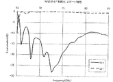
次に、1次放射器の構成例を図15および図16を参照して説明する。図15は誘電体ストリップ3を長手方向に通る断面図である。この誘電体ストリップ3によるNRDガイドと導波管4部分の構成は図1および図2に示した誘電体線路導波管変換器と基本的に同一である。ここで導波管4は、図における上面を開口面とするホーンアンテナを構成している。図中の円形のパターンはその概略放射パターンを示している。図16は上記放射パターンの実測例を示したものである。このように、円形空洞導波管の一端を開口した構造により、半値角の比較的広いビームが形成される。
【0034】
図17は他の1次放射器の構成を示す断面図である。この例では、導波管部分の開口面にテーパー部を設けている。この構造により、一般に放射パターンは軸方向に長く、軸に垂直な方向に短くなる。そして、その放射パターンは上記テーパー部の傾きと長さによって制御することができる。このことにより、半値角の比較的狭い、高利得のアンテナ装置を構成することができる。
【0035】
図18はさらに他の1次放射器の構成を示す断面図である。この例では、導波管の開口部付近に誘電体ロッド7を設けている。この構成によれば、誘電体ロッドアンテナとして作用し、誘電体ロッド7の長さと先端部のテーパー形状によって放射パターンが定まる。この構造によれば、図17に示した構造よりさらに指向性を鋭くすることができる。
【0036】
以上に示した各例では、簡単な構造で小型の1次放射器を構成することができる。また従来のように誘電体共振器に結合させてスロットから放射させるようにしたものではないので、広帯域特性を得ることができる。
【0037】
図19は上記各種1次放射器を用いたアンテナ装置の構成を示す断面図である。図19において10は1次放射器、11は誘電体レンズである。誘電体レンズ11は1次放射器10の同軸上に設けている。この構造により、指向性をさらに高めて高利得を得ることができる。
【0038】
次に、偏波制御を行った1次放射器の例を図20に示す。図20の(A)は開口面からみた上面図、(B)は正面図である。円形空洞導波管とNRDガイドとの関係は図1,図2または図15に示したものと同様であるが、この例では、誘電体ストリップ3の軸方向に対し平面図における交差角が約45°となる方向に、導波管内部を突出させ、これを縮退分離素子8として設けている。この縮退素子8は、縮退関係にある2つのモードを生じさせて、電界と磁界の位相に差を持たせる。これにより円偏波(楕円偏波を含む)の電磁波の放射を行う。したがって、NRDガイドからLSM01モードの送信信号が伝搬されれば、円偏波の電磁波が放射される。また、円偏波の電磁波が入射した場合、アンテナの可逆定理により、受信信号がLSM01モードでNRDガイドを伝搬することになる。
【0039】
図21は偏波制御を行う他の1次放射器の構成を示す図である。この例では、導波管4の内部にポーラライザ12を設けている。このポーザライザ12は偏波面を所定角度旋回させるものであり、誘電体ストリップ3の向きによって定まる円形空洞導波管の円形TE11モードの偏波面がポーラライザ12によって旋回されて放射される。入射波はポーラライザ12により旋回されてNRDガイドのLSM01モードに結合する。
【0040】
図22は更に他の偏波制御を行う1次放射器の構成を示す図である。図22の(A)は放射面からみた上面図、(B)は断面図である。この例では、導波管4の開口面にスロット板13を設けている。スロット板13にはスロット14を形成している。このスロット14からはスロット14の短軸方向を電界の向きとする電磁波が放射されるので、スロット14の向き(傾き)を定めることによって、偏波面の向きを定めることができる。
【0041】
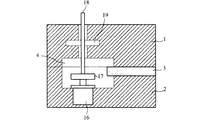
次に、誘電体線路導波管変換器を用いた発振器の例を図23に示す。図23において1,2は導体板であり、NRDガイドの上下の平行導体面および導波管4を構成する。ここでは導波管4は円形空洞共振器として用いる。誘電体ストリップ3の上下面は平行導体面の間に挟み込むように配置している。この図は、上下の導体板1,2および誘電体ストリップ3の軸方向に通る面での断面図であるので、NRDガイドの電磁波非伝搬領域は現れていないが、誘電体ストリップ3の両脇部分には空間部を設けていて、誘電体ストリップ3を電磁波伝搬領域とし、その両脇部分を電磁波非伝搬領域としている。導体板2にはガンダイオード16を取り付けていて、一方の端子を導体板2に接地し、他方の端子を突出させている。17は円板状の結合導体であり、ガンダイオード16の突出端子に取り付けている。また、18はガンダイオード16に対するバイアス電圧供給路であり、低誘電率の誘電体を介して、導体板1に設けた孔を通して取り付けている。この孔の途中部分には半径が管内波長の1/4の奇数倍の関係にある空洞部を設けて、これをトラップ19としている。
【0042】
この構成によって、ガンダイオード16の発振出力信号は結合導体17に導出され、結合導体17は導波管4による空洞共振器の共振モードを励振する。この空洞共振器の共振モードがNRDガイドのLSM01モードと結合して、そのモードで発振信号が伝搬されることになる。
【0043】
図24は他の発振器の構成を示す断面図である。図23と異なり、この図では、誘電体ストリップ3の端面が見える方向での断面図であり、空洞共振器としての導波管4の内部に温度補償用の誘電体20を設けている。この誘電体20の誘電率によって、導波管4による空洞共振器内の実効誘電率が定まるため、空洞共振器の共振周波数は温度補償用誘電体20の誘電率の変化によって変化する。したがって、ガンダイオード16の発振周波数の温度特性が安定するように、温度補償用誘電体20の誘電率温度特性を定めればよい。
【0044】
図25は更に他の発振器の構成を示す図であり、(A)は断面図、(B)は導波管内部の上面図である。この例では、空洞共振器としての導波管4の内部に回路基板21を配置している。この回路基板21には電極23と可変リアクタンス素子22およびこの可変リアクタンス素子22に対して制御電圧を供給する制御電圧供給路24を形成している。この制御電圧供給路24の途中にはスタブを設けていて、発振信号が制御電圧供給部側に回り込まないようにしている。電極23は結合導体17と電磁界結合するため、結局ガンダイオード16に対して可変リアクタンス素子のリアクタンス成分が装荷されたこととなる。したがって、可変リアクタンス素子22に対する制御電圧によってガンダイオード16の発振周波数を制御することができる。
【0045】
次に、ミリ波レーダに用いる送受波モジュールの例を図26に示す。図26においてVCOは図25に示した発振周波数可変のオシレータである。またアンテナは上記各種1次放射器のいずれかと誘電体レンズとにより構成する。図26においてVCOの出力信号はアイソレータ→カップラ→サーキュレータの経路でアンテナから送信され、アンテナで受信した信号がサーキュレータを介してミキサに供給される。またミキサはこの受信信号RXとカップラで分配したローカル信号Loとをミキシングして、送信信号と受信信号の周波数差を中間周波信号IFとして出力する。図外の制御回路はVCOの発振信号を変調すると共に、IF信号からターゲットまでの距離と相対速度を求める。
【0046】
次に、他の誘電体線路導波管変換器の例を図27を参照して説明する。
図27は誘電体線路導波管変換器の主要部の斜視図である。DWGで示す部分は導電性管内に誘電体を装荷(充填)した誘電体線路(DWG)である。4は円形の空洞導波管である。
【0047】
図27において実線の矢印は電界分布、それに直交する破線は磁界分布をそれぞれ示している。上記DWGの基本モードはTE01モードであり、図27に示すように、この誘電体線路の電磁波伝搬方向に、上下の導体面に対して垂直方向に磁界が向くモードとなる。一方の円形空洞導波管の基本モードは円形TE11モードであり、図27に示すように、DWGのTE01モードの磁界と円形空洞導波管の円形TE11モードの磁界の向きが揃う方向に電磁界が分布することになる。このように誘電体線路のTE01モードと円形空洞導波管のTE11モードとが電磁界結合して線路変換が行われる。
【0048】
図28は、図27に示した誘電体線路導波管変換器で用いたDWGの分散曲線と、図1に示した誘電体線路導波管変換器で用いたNRDガイドの分散曲線との比較例を示したものである。この図の(B)に示すように、NRDガイドでは、使用周波数帯である60GHz帯において平行平板モードが遮断されず、導波管との変換部付近では、主たる伝搬モードとして用いるLSM01モードから、スプリアスモードである平行平板モードに変換されて、平行平板モードが発生し易くなる。これに対して、図の(A)に示すように、DWGでは、使用周波数帯である60GHz帯においては、平行平板モードの位相定数βが0になる遮断周波数が、使用周波数帯である60GHzより高いため、使用周波数帯で平行平板モードは遮断され、平行平板モードの影響を受けない。
【0049】
次に、ミリ波レーダモジュールの構成例を図29〜図31を基に説明する。 図29は上部の導体板を取り除いた状態での上面図である。このミリ波レーダモジュールは、大別してオシレータ、アイソレータ、方向性結合器、サーキュレータ、ミキサ、1次放射器の各ユニットからなる。オシレータはガンダイオードによりミリ波信号を発生する。アイソレータは図に示すように3つの誘電体ストリップをポートとするサーキュレータの1つのポートに終端器を接続することによって構成している。すなわちオシレータからのミリ波信号を方向性結合器側へ伝搬させ、方向性結合器からの反射信号を終端器へ導くようにしている。方向性結合器はNRDガイドによる4つのポートを備え、所定の電力分配比で、ポート#1からの入力信号をポート#3とポート#4へ分配する。ポート#3からの信号はサーキュレータを経て0dBカプラへ出力される。
【0050】
この0dBカプラは、可動部が図に示す矢印方向に変位しても、可動部側に設けた誘電体ストリップと、固定部側の誘電体ストリップとの間が、常に略0dBの挿入損失で結合する結合器である。この0dBカプラの固定部側と可動部側の誘電体ストリップは、それぞれ上下の導体板で挟まれてNRDガイドを構成している。また、可動部側のNRDガイドはDWGに線路変換し、そのDWGと円形空洞導波管とで、図27に示したものと同様の誘電体線路導波管変換器を構成している。
上記円形空洞導波管の前方には、その軸方向に所定距離離れた位置に誘電体レンズを設けている。したがって、可動部の図に示す矢印方向に変位によって、アンテナの指向方向が変化する。
【0051】
サーキュレータからの送信信号はアンテナから所定指向方向のターゲットに向けて送波される。アンテナで受けたターゲットからの反射信号はサーキュレータを介してミキサに受信信号として入力される。一方、方向性結合器のポート#4からの信号がローカル信号としてミキサに入力され、ミキサは受信信号とローカル信号とをミキシングする。オシレータの信号がたとえば時間的に2値の周波数f1,f2をとる場合、2経路の経路差により生じる時間差に応じたf1−f2の周波数成分を持つIF信号が得られる。このIF信号を信号処理することによりターゲットまでの測距を行う。
図29に示したミリ波レーダモジュールのブロック図は図26に示したものと同様である。
【0052】
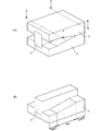
図30は上記NRDガイドとDWGとの線路変換部の構造を示している。(A)は主要部の全体の斜視図、(B)は(A)の上部の導体板を取り除いた状態での斜視図である。図30において1,2はそれぞれ導体板、3は誘電体ストリップである。図に示すように、上下の導体板1,2の間に誘電体ストリップ3を配置することによってNRDガイド、DWGおよびその間のTRで示す線路変換部を構成している。
【0053】
誘電体ストリップ3の高さおよび幅方向の寸法はNRDガイド、DWGおよび線路変換部TRのいずれにおいても一定である。NRDガイド部分において、上下の導体板の対向面(導体面)の間隔を誘電体ストリップ3の高さ寸法より狭い所定寸法に形成している。これによりLSM01モードの単一モードを伝搬するNRDガイドを構成している。DWG部分では、上下の導体板1,2を重ねた状態すなわち対向面の間隔がほぼ0となるようにしている。これにより誘電体装荷線路を構成している。
【0054】
線路変換部TRでは、上下の導体板1,2の対向面の間隔がNRDガイド部分からDWG部分にかけてテーパー状となるように、導体板の間隔を順次変化させている。この構造により線路変換部TRの入出力部分および途中での反射を低減し、線路変換器としての反射特性を良好に保っている。
【0055】
図31はミリ波レーダモジュールの1次放射器の反射特性を示す図、図32は上記1次放射器と誘電体レンズによるアンテナの利得特性を示す図であり、(A)は図29に示した構成による特性、(B)は図29に示した可動部の誘電体線路をNRDガイドで構成したときの特性をそれぞれ示している。このように、DWGを導波管モードに変換する1次放射器を用いれば、平行平板モードによる悪影響を受けないので、アンテナ利得の周期的な減衰がなく、良好なアンテナ特性を得ることができる。
【0056】
なお、各実施形態では導波管部分を空洞導波管として構成したが、この部分を空気以外の誘電体を充填した導波管としてもよい。
【0057】
また、各実施形態では、導波管の内部に誘電体線路の誘電体部分を所定量挿入した例を示したが、必ずしも「挿入」状態になくてもよく、導波管の内部にNRDガイドやDWG等の誘電体線路の誘電体部分が近接するように配置してもよい。
【0058】
【発明の効果】
請求項1に係る発明によれば、誘電体線路の誘電体ストリップ端部から軸方向への放射構造を用いていないため、不要な放射がなく、誘電体線路と導波管との線路変換を低損失で行うことができる。また、誘電体線路と導波管との電磁波伝搬方向が直交関係にあるので、回路構成上の設計上の自由度が高まり、全体に小型化を図ることができる。
【0060】
請求項2に係る発明によれば、誘電体線路の平行導体面の一方が前記導波管の端面に連続するため、誘電体線路と導波管とを容易に整合させることができる。
【0061】
請求項3に係る発明によれば、誘電体線路と導波管とを容易に整合させることができる。
【0062】
請求項4に係る発明によれば、各誘電体線路と導波管とによって誘電体線路導波管変換器を構成するので、複数の誘電体線路は導波管を介して接続されることになる。そのため、導波管に対する誘電体線路の誘電体ストリップの挿入位置(高さ)および方向を変えることによって、誘電体線路の多層化および伝搬方向の変換を容易に行えるようになる。
【0063】
請求項5に係る発明によれば、誘電体線路を伝搬路とする1次放射器を容易に構成することができ、しかも広帯域特性を得ることができる。
【0064】
請求項6に係る発明によれば、発振素子の発振出力信号が導波管の共振モードを介して誘電体線路の伝搬モードに変換される。そのため、誘電体線路を介して発振信号を容易に伝送できるようになる。
【0065】
請求項7,8に係る発明によれば、小型、低損失、および広帯域の送信装置が得られる。
【図面の簡単な説明】
【図1】誘電体線路導波管変換器の主要部の構成を示す斜視図
【図2】同誘電体線路導波管変換器の構成を示す図
【図3】同誘電体線路導波管変換器の特性図
【図4】整合調整手段を備えた誘電体線路導波管変換器の構成を示す図
【図5】整合調整を行った誘電体線路導波管変換器の構成を示す図
【図6】矩形導波管を用いた誘電体線路導波管変換器の主要部の構成を示す斜視図
【図7】誘電体線路接続構造の例を示す断面図
【図8】同誘電体線路接続構造の特性図
【図9】3ポートの誘電体線路接続構造の例を示す断面図
【図10】同誘電体線路接続構造の特性図
【図11】3ポートの誘電体線路接続構造の他の例を示す断面図
【図12】同誘電体線路接続構造の特性図
【図13】誘電体線路接続構造の平面図
【図14】入出力ポートの角度関係を可変とした誘電体線路接続構造の例を示す断面図
【図15】1次放射器の構成を示す断面図
【図16】図15に示す1次放射器の放射パターンを示す図
【図17】他の1次放射器の構成を示す断面図
【図18】更に他の1次放射器の構成を示す断面図
【図19】1次放射器を用いたアンテナ装置の構成を示す断面図
【図20】偏波制御手段を設けた1次放射器の構成を示す図
【図21】偏波制御手段を設けた1次放射器の構成を示す図
【図22】偏波制御手段を設けた1次放射器の構成を示す図
【図23】発振器の構成を示す断面図
【図24】発振器の構成を示す断面図
【図25】発振器の構成を示す断面図および上面図
【図26】送受波モジュールの構成を示すブロック図
【図27】誘電体線路導波管変換器の主要部の構成を示す斜視図
【図28】同変換器で用いる誘電体装荷線路DWGと、比較例としてのNRDガイドとの分散曲線を示す図
【図29】ミリ波レーダモジュールの構成を示す図
【図30】同ミリ波レーダモジュールで用いる線路変換部の構造を示す斜視図
【図31】同ミリ波レーダモジュールの1次放射器の反射特性と、その比較例を示す図
【図32】同ミリ波レーダモジュールのアンテナ利得特性と、その比較例を示す図
【符号の説明】
1,2−導体板
3−誘電体ストリップ
4−導波管
5−整合用突出部
6−ネジ
7−誘電体ロッド
8−縮退分離素子
10−1次放射器
11−誘電体レンズ
12−ポーラライザ
13−スロット板
14−スロット
16−ガンダイオード
17−結合導体
18−バイアス電圧供給路
19−トラップ
20−誘電体
21−回路基板
22−可変リアクタンス素子
23−電極
24−制御電圧供給路
NRD−非放射性誘電体線路
DWG−誘電体装荷線路[0001]
BACKGROUND OF THE INVENTION
This invention Non-radioactive Dielectric line (Hereafter, it is simply called “dielectric line”.) The present invention relates to a line converter between a waveguide and a waveguide, a connection structure between a plurality of dielectric lines, a primary radiator using a dielectric line and a waveguide, an oscillator, and a transmission device using them.
[0002]
[Prior art]
Dielectric lines and waveguides are used as high-frequency circuit lines in the microwave band and millimeter wave band. When both lines are mixed, a line converter between the dielectric line and the waveguide is required. . Therefore, conventionally, for example, as shown in (1) Japanese Patent Application No. 6-205424, the tip of the dielectric strip of the dielectric line is tapered, and the end of the waveguide is widened in a horn shape. Thus, a line conversion unit between the dielectric line and the waveguide is formed.
[0003]
Further, when a circuit is configured using a large number of dielectric lines, not only a dielectric strip is arranged on the same plane, but also a structure for transmitting a signal from one plane to another plane is required. Therefore, in the prior art, as shown in (2) Japanese Patent Laid-Open No. 8-181502, a hole is formed in a conductor plate at an intersection where a plurality of dielectric lines should be crossed in layers, and a position where the dielectric strip faces the hole The radio wave reflector is arranged so as to face the open end.
[0004]
In addition, as an antenna device for transmitting and receiving electromagnetic waves in the millimeter wave band and microwave band, a dielectric resonator is disposed on the extension line in the vicinity of the end of the dielectric strip, and the dielectric strip and the dielectric resonator. (3) Japanese Patent Laid-Open No. 8-316727 shows an antenna device in which a primary radiator is formed by forming a slot in one conductor plate that sandwiches a substrate, and a dielectric lens is arranged in the axial direction of the dielectric resonator. ing.
[0005]
[Problems to be solved by the invention]
However, in the structure of the dielectric line waveguide converter of (1), the end face of the dielectric strip of the line conversion part and the metal part of the dielectric line and the waveguide need to be processed into a special shape. It was. Further, since the electromagnetic wave propagation directions of the dielectric line and the waveguide are linear, the degree of freedom in circuit design is low, and the entire circuit may be enlarged. In addition, a rectangular waveguide is used as the waveguide, and line conversion cannot be performed directly on the circular waveguide.
[0006]
In the multistage three-dimensional intersection structure of (2), a radio wave reflector must be provided at the three-dimensional intersection, which is complicated in structure and difficult to manufacture.
[0007]
Further, the primary radiator using the dielectric line of (3) has a problem that the frequency band that can be used as the primary radiator is narrow due to the characteristics of the dielectric resonator.
[0008]
An object of the present invention is to provide a dielectric line waveguide converter, a dielectric line connection structure, a primary radiator, an oscillator, and a transmission device using these, which have solved the above-mentioned various problems.
[0009]
[Means for Solving the Problems]
The dielectric line waveguide converter according to the present invention is configured so that the dielectric of the dielectric line in the waveguide is substantially perpendicular to the electromagnetic wave propagation direction of the waveguide. Insert a certain amount of the end Constitute.
According to this structure, since the radiation structure from the end of the dielectric portion of the dielectric line to the axial direction is not used, there is no unnecessary radiation, and line conversion between the dielectric line and the waveguide can be performed with low loss. It can be carried out. Further, since the electromagnetic wave propagation directions between the dielectric line and the waveguide are orthogonal, the degree of freedom in designing the circuit configuration is increased, and the overall size can be reduced.
[0011]
In the dielectric line waveguide converter of the present invention, one of the parallel conductor surfaces of the dielectric line is made continuous with the end face of the waveguide. With this structure, the dielectric line and the waveguide can be easily matched.
[0012]
Further, in the line conversion portion between the dielectric line and the waveguide, the cross-sectional shape of the waveguide is partially changed. This makes it easy to match both lines.
[0013]
The dielectric line connection structure of the present invention is configured by providing a plurality of dielectric lines in the dielectric line waveguide converter and inserting a part of each dielectric strip into the waveguide. That is, since each dielectric line and the waveguide constitute a dielectric line waveguide converter, a plurality of dielectric lines are connected via the waveguide. Therefore, by changing the insertion position (height) and direction of the dielectric strip of the dielectric line with respect to the waveguide, it becomes possible to easily make the dielectric line multilayer and change the propagation direction.
[0014]
A primary radiator according to the present invention includes a primary radiator having an opening at one end of the waveguide in the dielectric line waveguide converter or the dielectric line connection structure and having the end face as an opening surface. Constitute. With this structure, it is possible to easily configure a primary radiator having a dielectric line as a propagation path, and to obtain broadband characteristics.
[0015]
The oscillator according to the present invention includes an oscillation element in the waveguide. And a coupling conductor for deriving an oscillation output signal of the oscillation element and coupling to a resonance mode of the waveguide. . With this structure, the oscillation output signal of the oscillation element is converted into the propagation mode of the dielectric line via the resonance mode of the waveguide. Therefore, the oscillation signal can be easily transmitted through the dielectric line.
[0016]
A transmitting apparatus according to the present invention includes an antenna device provided with the dielectric radiator and a primary radiator made of a waveguide, and an oscillator that generates a transmission signal for the antenna device. In addition, the oscillator includes a dielectric line and a waveguide, and an antenna device that transmits an output signal of the oscillator is provided. As a result, a small-sized, low-loss, and wide-band transmission device can be obtained.
[0017]
DETAILED DESCRIPTION OF THE INVENTION
The configuration of the dielectric waveguide converter according to the first embodiment of the present invention will be described with reference to FIGS.
FIG. 1 is a perspective view of a main part of a dielectric line waveguide converter, FIG. 2 is a diagram showing a configuration of the converter, (A) is a top view, and (B) is a BB portion in (A). (C) is sectional drawing of CC part in (A). In FIG. 2,
[0018]
FIG. 1 shows the positional relationship between the inner surface of the
[0019]
As the inner diameter φa of the circular cavity waveguide, a value normalized according to the frequency band is used. For example, in the 76 GHz band, φa = 2.8 mm. An insertion amount E of the
[0020]
In FIG. 1, solid arrows indicate electric field distributions, and broken lines perpendicular thereto indicate magnetic field distributions. The basic mode of the NRD guide is the LSM01 mode, which is a mode in which the magnetic field is directed in the direction of electromagnetic wave propagation of the dielectric strip in the direction perpendicular to the upper and lower conductor plates as shown in FIG. The fundamental mode of one of the circular cavity waveguides is the circular TE11 mode. As shown in FIG. 1, the direction of the magnetic field of the LSM01 mode of the dielectric line and that of the circular TE11 mode of the circular cavity waveguide are aligned. The electromagnetic field will be distributed. In this way, the LSM01 mode of the dielectric line and the TE11 mode of the circular cavity waveguide are electromagnetically coupled to perform line conversion.
[0021]
FIG. 3 shows the reflection characteristics viewed from the NRD guide under these conditions. Thus, by appropriately determining the amount of insertion of the dielectric strip, line conversion between the dielectric line and the waveguide can be performed with a low reflection characteristic in a predetermined frequency band.
[0022]
In the structure shown in FIGS. 1 and 2, the
[0023]
Next, an example of a dielectric line waveguide converter having matching adjusting means will be described with reference to FIGS. In the example shown in FIG. 4A, an
In the example shown in FIG. 4B, a screw 6 capable of adjusting the amount of insertion into the waveguide is provided as the alignment protrusion. Adjustment of the screw 6 makes it possible to adjust to an optimum alignment state.
[0024]
In each of the examples described above, the tip of the dielectric strip inserted into the waveguide has a shape perpendicular to the electromagnetic wave propagation direction. However, other shapes may be used. FIG. 5 is a plan view of the dielectric line waveguide converter. As shown in FIG. 5A, the tip of the
[0025]
Next, FIG. 6 shows a configuration of a dielectric line waveguide converter according to the third embodiment. FIG. 6A is a perspective view showing the positional relationship between the inner wall surface of the waveguide and the dielectric strip of the NRD guide, and FIG. 6B is a plan view seen from the opening surface side of the waveguide. Unlike the dielectric line waveguide converter shown in FIGS. 1 and 2, the
[0026]
Even when the rectangular hollow waveguide is used as described above, the insertion amount of the
[0027]
Next, a dielectric line connection structure according to a fourth embodiment will be described with reference to FIGS.
FIG. 7 is a cross-sectional view through the respective dielectric strip portions of the two dielectric lines.
[0028]
FIG. 8 shows the reflection characteristics between the two ports in FIG. 7 with φa = 2.8 mm, L = 1.1 mm, H = 1.8 mm, E = 0.4 mm, and using the two NRD guides as input / output ports. S11 and transmission characteristics S21 are obtained. In this example, a low insertion loss characteristic is obtained over a wide band of 70 to 75 GHz, and the reflection loss is the smallest in the 73 GHz band. In this way, two NRD guides can be connected to each other with low reflection and low insertion loss in a predetermined frequency band.
[0029]
Next, a dielectric line connection structure according to a fifth embodiment will be described with reference to FIGS.
FIG. 9 is a cross-sectional view through each dielectric strip portion as shown in FIG. In this example, three NRD guide
[0030]
FIG. 11 and FIG. 12 are diagrams showing a dielectric line connection structure and its characteristics according to the sixth embodiment. FIG. 11 is a cross-sectional view passing through each dielectric strip portion as shown in FIG. In this example, three NRD guide
[0031]
7, 9, and 11, the positional relationship between the dielectric strips is shown as a cross-sectional view. However, the planar relationship may be as shown in FIG. In FIG. 13A, two
[0032]
Next, a dielectric line connection structure according to a seventh embodiment is shown in FIG. In this example, the circular
[0033]
Next, a configuration example of the primary radiator will be described with reference to FIGS. 15 and 16. FIG. 15 is a sectional view passing through the
[0034]
FIG. 17 is a cross-sectional view showing the configuration of another primary radiator. In this example, a tapered portion is provided on the opening surface of the waveguide portion. With this structure, the radiation pattern is generally long in the axial direction and short in the direction perpendicular to the axis. The radiation pattern can be controlled by the inclination and length of the tapered portion. As a result, a high gain antenna apparatus having a relatively narrow half-value angle can be configured.
[0035]
FIG. 18 is a sectional view showing the configuration of still another primary radiator. In this example, a dielectric rod 7 is provided near the opening of the waveguide. According to this configuration, it acts as a dielectric rod antenna, and the radiation pattern is determined by the length of the dielectric rod 7 and the tapered shape of the tip. According to this structure, the directivity can be made sharper than the structure shown in FIG.
[0036]
In each example shown above, a small primary radiator can be configured with a simple structure. Further, since it is not coupled to a dielectric resonator and radiated from a slot as in the prior art, a wide band characteristic can be obtained.
[0037]
FIG. 19 is a cross-sectional view showing a configuration of an antenna device using the various primary radiators. In FIG. 19, 10 is a primary radiator and 11 is a dielectric lens. The
[0038]
Next, FIG. 20 shows an example of a primary radiator that performs polarization control. 20A is a top view seen from the opening surface, and FIG. 20B is a front view. The relationship between the circular cavity waveguide and the NRD guide is the same as that shown in FIG. 1, FIG. 2 or FIG. 15, but in this example, the crossing angle in the plan view with respect to the axial direction of the
[0039]
FIG. 21 is a diagram showing the configuration of another primary radiator that performs polarization control. In this example, a
[0040]
FIG. 22 is a diagram showing a configuration of a primary radiator that performs another polarization control. 22A is a top view seen from the radiation surface, and FIG. 22B is a cross-sectional view. In this example, a
[0041]
Next, FIG. 23 shows an example of an oscillator using a dielectric line waveguide converter. In FIG. 23,
[0042]
With this configuration, the oscillation output signal of the
[0043]
FIG. 24 is a cross-sectional view showing the configuration of another oscillator. Unlike FIG. 23, this figure is a cross-sectional view in a direction in which the end face of the
[0044]
FIG. 25 is a diagram showing the configuration of still another oscillator, in which (A) is a cross-sectional view and (B) is a top view inside the waveguide. In this example, the
[0045]
Next, FIG. 26 shows an example of a transmission / reception module used for the millimeter wave radar. In FIG. 26, VCO is an oscillator with variable oscillation frequency shown in FIG. The antenna is composed of any one of the various primary radiators and a dielectric lens. In FIG. 26, the output signal of the VCO is transmitted from the antenna through the path of isolator → coupler → circulator, and the signal received by the antenna is supplied to the mixer via the circulator. The mixer mixes the reception signal RX and the local signal Lo distributed by the coupler, and outputs the frequency difference between the transmission signal and the reception signal as an intermediate frequency signal IF. A control circuit (not shown) modulates the oscillation signal of the VCO and determines the distance and relative speed from the IF signal to the target.
[0046]
Next, an example of another dielectric line waveguide converter will be described with reference to FIG.
FIG. 27 is a perspective view of the main part of the dielectric waveguide converter. A portion indicated by DWG is a dielectric line (DWG) in which a dielectric is loaded (filled) in a conductive tube. 4 is a circular cavity waveguide.
[0047]
In FIG. 27, solid arrows indicate electric field distributions, and broken lines perpendicular to the electric field distributions indicate magnetic field distributions. The basic mode of the DWG is a TE01 mode, and as shown in FIG. 27, a magnetic field is directed in a direction perpendicular to the upper and lower conductor surfaces in the electromagnetic wave propagation direction of the dielectric line. The fundamental mode of one circular cavity waveguide is a circular TE11 mode. As shown in FIG. 27, the electromagnetic field is in a direction in which the directions of the magnetic field of the TE01 mode of the DWG and the magnetic field of the circular TE11 mode of the circular cavity waveguide are aligned. Will be distributed. In this way, the TE01 mode of the dielectric line and the TE11 mode of the circular cavity waveguide are electromagnetically coupled to perform line conversion.
[0048]
28 is a comparison between the dispersion curve of the DWG used in the dielectric line waveguide converter shown in FIG. 27 and the dispersion curve of the NRD guide used in the dielectric line waveguide converter shown in FIG. An example is shown. As shown in (B) of this figure, in the NRD guide, the parallel plate mode is not cut off in the used frequency band of 60 GHz, and from the LSM01 mode used as the main propagation mode in the vicinity of the conversion section with the waveguide, The parallel plate mode, which is a spurious mode, is easily converted to the parallel plate mode. On the other hand, as shown in (A) of the figure, in the DWG, in the 60 GHz band that is the use frequency band, the cut-off frequency at which the phase constant β of the parallel plate mode is 0 is lower than the use frequency band of 60 GHz. Since it is high, the parallel plate mode is cut off in the operating frequency band and is not affected by the parallel plate mode.
[0049]
Next, a configuration example of the millimeter wave radar module will be described with reference to FIGS. FIG. 29 is a top view with the upper conductor plate removed. This millimeter wave radar module is roughly composed of units of an oscillator, an isolator, a directional coupler, a circulator, a mixer, and a primary radiator. The oscillator generates a millimeter wave signal by a Gunn diode. As shown in the figure, the isolator is configured by connecting a terminator to one port of a circulator having three dielectric strips as ports. That is, the millimeter wave signal from the oscillator is propagated to the directional coupler side, and the reflected signal from the directional coupler is guided to the terminator. The directional coupler has four ports by the NRD guide, and distributes the input signal from the
[0050]
In this 0 dB coupler, even when the movable part is displaced in the direction of the arrow shown in the figure, the dielectric strip provided on the movable part side and the dielectric strip on the fixed part side are always coupled with an insertion loss of approximately 0 dB. It is a coupler. The fixed strip side and movable portion side dielectric strips of this 0 dB coupler are sandwiched between upper and lower conductor plates to form an NRD guide. Further, the NRD guide on the movable portion side converts the line to DWG, and the DWG and the circular cavity waveguide constitute a dielectric line waveguide converter similar to that shown in FIG.
A dielectric lens is provided in front of the circular cavity waveguide at a position separated by a predetermined distance in the axial direction. Therefore, the directivity direction of the antenna changes due to the displacement in the arrow direction shown in the drawing of the movable part.
[0051]
A transmission signal from the circulator is transmitted from the antenna toward a target in a predetermined directivity direction. The reflected signal from the target received by the antenna is input as a received signal to the mixer via the circulator. On the other hand, a signal from
The block diagram of the millimeter wave radar module shown in FIG. 29 is the same as that shown in FIG.
[0052]
FIG. 30 shows the structure of the line conversion unit between the NRD guide and the DWG. (A) is a perspective view of the whole main part, (B) is a perspective view in the state which removed the upper conductor board of (A). In FIG. 30, 1 and 2 are conductor plates, and 3 is a dielectric strip. As shown in the figure, by arranging the
[0053]
The dimensions of the
[0054]
In the line conversion unit TR, the interval between the conductor plates is sequentially changed so that the interval between the opposing surfaces of the upper and
[0055]
FIG. 31 is a diagram showing the reflection characteristics of the primary radiator of the millimeter wave radar module, FIG. 32 is a diagram showing the gain characteristics of the antenna by the primary radiator and the dielectric lens, and (A) is shown in FIG. (B) shows the characteristics when the dielectric line of the movable part shown in FIG. 29 is configured with an NRD guide. As described above, if the primary radiator that converts the DWG into the waveguide mode is used, since it is not adversely affected by the parallel plate mode, the antenna gain is not periodically attenuated, and good antenna characteristics can be obtained. .
[0056]
In each embodiment, the waveguide portion is configured as a hollow waveguide, but this portion may be a waveguide filled with a dielectric other than air.
[0057]
In each embodiment, an example in which a predetermined amount of the dielectric portion of the dielectric line is inserted into the waveguide has been described. However, the NRD guide may not necessarily be in the “insertion” state. Or a dielectric part of a dielectric line such as DWG may be arranged close to each other.
[0058]
【The invention's effect】
According to the first aspect of the present invention, since the radiation structure from the end of the dielectric strip of the dielectric line to the axial direction is not used, there is no unnecessary radiation, and the line conversion between the dielectric line and the waveguide is performed. Can be done with low loss. Further, since the electromagnetic wave propagation directions between the dielectric line and the waveguide are orthogonal, the degree of freedom in designing the circuit configuration is increased, and the overall size can be reduced.
[0060]
[0061]
[0062]
[0063]
[0064]
Claim 6 According to the invention, the oscillation output signal of the oscillation element is converted into the propagation mode of the dielectric line through the resonance mode of the waveguide. Therefore, the oscillation signal can be easily transmitted through the dielectric line.
[0065]
[Brief description of the drawings]
FIG. 1 is a perspective view showing a configuration of a main part of a dielectric line waveguide converter.
FIG. 2 is a diagram showing a configuration of the dielectric line waveguide converter
FIG. 3 is a characteristic diagram of the dielectric line waveguide converter.
FIG. 4 is a diagram showing a configuration of a dielectric line waveguide converter provided with matching adjustment means.
FIG. 5 is a diagram showing the configuration of a dielectric line waveguide converter that has been adjusted for matching;
FIG. 6 is a perspective view showing a configuration of a main part of a dielectric line waveguide converter using a rectangular waveguide.
FIG. 7 is a cross-sectional view showing an example of a dielectric line connection structure
FIG. 8 is a characteristic diagram of the dielectric line connection structure.
FIG. 9 is a sectional view showing an example of a 3-port dielectric line connection structure;
FIG. 10 is a characteristic diagram of the dielectric line connection structure.
FIG. 11 is a sectional view showing another example of a 3-port dielectric line connection structure;
FIG. 12 is a characteristic diagram of the dielectric line connection structure.
FIG. 13 is a plan view of a dielectric line connection structure.
FIG. 14 is a cross-sectional view showing an example of a dielectric line connection structure in which the angular relationship of input / output ports is variable
FIG. 15 is a cross-sectional view showing the configuration of a primary radiator
16 is a view showing a radiation pattern of the primary radiator shown in FIG.
FIG. 17 is a cross-sectional view showing the configuration of another primary radiator
FIG. 18 is a cross-sectional view showing the configuration of still another primary radiator.
FIG. 19 is a cross-sectional view illustrating a configuration of an antenna device using a primary radiator.
FIG. 20 is a diagram showing a configuration of a primary radiator provided with polarization control means.
FIG. 21 is a diagram showing a configuration of a primary radiator provided with polarization control means.
FIG. 22 is a diagram showing a configuration of a primary radiator provided with polarization control means.
FIG. 23 is a cross-sectional view showing a configuration of an oscillator.
FIG. 24 is a cross-sectional view showing the configuration of an oscillator
FIG. 25 is a cross-sectional view and a top view showing the configuration of the oscillator.
FIG. 26 is a block diagram showing a configuration of a transmission / reception module.
FIG. 27 is a perspective view showing a configuration of a main part of a dielectric line waveguide converter.
FIG. 28 is a diagram showing a dispersion curve of a dielectric loaded line DWG used in the converter and an NRD guide as a comparative example;
FIG. 29 is a diagram showing the configuration of a millimeter wave radar module
FIG. 30 is a perspective view showing a structure of a line converter used in the millimeter wave radar module.
FIG. 31 is a diagram showing a reflection characteristic of a primary radiator of the millimeter wave radar module and a comparative example thereof.
FIG. 32 is a diagram showing antenna gain characteristics of the millimeter-wave radar module and a comparative example thereof
[Explanation of symbols]
1,2-conductor plate
3-dielectric strip
4-waveguide
5-Alignment protrusion
6-screw
7-Dielectric rod
8-degenerate separation element
10-1 primary radiator
11-dielectric lens
12-Polarizer
13-slot plate
14-slot
16-Gun diode
17-Coupling conductor
18-Bias voltage supply path
19-trap
20-dielectric
21-circuit board
22-Variable reactance element
23-electrode
24-Control voltage supply path
NRD-Non-radiative dielectric line
DWG-dielectric loading line
Claims (8)
導波管の電磁波伝搬方向に対して略垂直方向に、当該導波管内に前記非放射性誘電体線路の誘電体の端部を一定量挿入して成る非放射性誘電体線路導波管変換器。A line converter between a non-radiative dielectric line and a waveguide,
In a direction substantially perpendicular to the electromagnetic wave propagation direction of the waveguide, a nonradiative dielectric waveguide converter comprising an end portion of the dielectric of said to said waveguide nonradiative dielectric waveguide is inserted a predetermined amount.
Priority Applications (1)
| Application Number | Priority Date | Filing Date | Title |
|---|---|---|---|
| JP35992999A JP3617397B2 (en) | 1998-12-25 | 1999-12-17 | Dielectric line waveguide converter, dielectric line connection structure, primary radiator, oscillator, and transmitter |
Applications Claiming Priority (3)
| Application Number | Priority Date | Filing Date | Title |
|---|---|---|---|
| JP36993298 | 1998-12-25 | ||
| JP10-369932 | 1998-12-25 | ||
| JP35992999A JP3617397B2 (en) | 1998-12-25 | 1999-12-17 | Dielectric line waveguide converter, dielectric line connection structure, primary radiator, oscillator, and transmitter |
Related Child Applications (1)
| Application Number | Title | Priority Date | Filing Date |
|---|---|---|---|
| JP2003394467A Division JP2004120792A (en) | 1998-12-25 | 2003-11-25 | Waveguide conversion structure, waveguide connection structure, primary radiator, oscillator and transmission apparatus |
Publications (2)
| Publication Number | Publication Date |
|---|---|
| JP2000244210A JP2000244210A (en) | 2000-09-08 |
| JP3617397B2 true JP3617397B2 (en) | 2005-02-02 |
Family
ID=26581039
Family Applications (1)
| Application Number | Title | Priority Date | Filing Date |
|---|---|---|---|
| JP35992999A Expired - Fee Related JP3617397B2 (en) | 1998-12-25 | 1999-12-17 | Dielectric line waveguide converter, dielectric line connection structure, primary radiator, oscillator, and transmitter |
Country Status (1)
| Country | Link |
|---|---|
| JP (1) | JP3617397B2 (en) |
Families Citing this family (3)
| Publication number | Priority date | Publication date | Assignee | Title |
|---|---|---|---|---|
| KR100815154B1 (en) * | 2007-02-27 | 2008-03-19 | 한국전자통신연구원 | Multiband antenna feeder for satellite communications organized waveguide |
| JP2011254418A (en) * | 2010-06-04 | 2011-12-15 | Toko Inc | Connection structure of cavity waveguide and dielectric waveguide |
| JP6446331B2 (en) | 2015-06-08 | 2018-12-26 | 日立オートモティブシステムズ株式会社 | Sensor with flat beam generating antenna |
Family Cites Families (8)
| Publication number | Priority date | Publication date | Assignee | Title |
|---|---|---|---|---|
| JPS6157701U (en) * | 1984-09-19 | 1986-04-18 | ||
| JPH02199903A (en) * | 1989-01-27 | 1990-08-08 | Chubu Nippon Hoso Kk | Dielectric transmission line |
| KR960036200A (en) * | 1995-03-31 | 1996-10-28 | 배순훈 | Structure of Planar Antenna for Dual Polarization Reception |
| JP3412353B2 (en) * | 1995-08-31 | 2003-06-03 | 株式会社村田製作所 | Jig for measuring characteristics of non-radiative dielectric line component and method for measuring characteristics of non-radiative dielectric line component |
| JP3442920B2 (en) * | 1995-11-17 | 2003-09-02 | 株式会社日立国際電気 | NRD guide circularly polarized antenna |
| JPH11308021A (en) * | 1998-04-23 | 1999-11-05 | Nec Corp | Connection structure for high frequency package |
| JP3723687B2 (en) * | 1998-06-29 | 2005-12-07 | 京セラ株式会社 | Connection structure between NRD guide and dielectric waveguide |
| JP3899187B2 (en) * | 1998-06-30 | 2007-03-28 | 新日本無線株式会社 | Non-radioactive dielectric guide circuit |
-
1999
- 1999-12-17 JP JP35992999A patent/JP3617397B2/en not_active Expired - Fee Related
Also Published As
| Publication number | Publication date |
|---|---|
| JP2000244210A (en) | 2000-09-08 |
Similar Documents
| Publication | Publication Date | Title |
|---|---|---|
| CA2292064C (en) | Line transition device between dielectric waveguide and waveguide, and oscillator and transmitter using the same | |
| US7642979B2 (en) | Wave-guide-notch antenna | |
| EP0871239B1 (en) | Antenna device and radar module | |
| JP3473576B2 (en) | Antenna device and transmitting / receiving device | |
| US7212087B2 (en) | Twisted waveguide and wireless device | |
| JP3186622B2 (en) | Antenna device and transmitting / receiving device | |
| EP0817394B1 (en) | Transmitter-receiver | |
| EP0996189A2 (en) | Dielectric line converter, dielectric line unit, directional coupler, high-frequency circuit module, and transmitter-receiver | |
| US6133887A (en) | Antenna device, and transmitting/receiving unit | |
| CA2256283C (en) | Non radiative dielectric waveguide having a portion for line conversion between different types of non radiative dielectric waveguides | |
| EP0969545B1 (en) | Directional coupler, antenna device, and transceiver | |
| JP3617397B2 (en) | Dielectric line waveguide converter, dielectric line connection structure, primary radiator, oscillator, and transmitter | |
| JP2004120792A (en) | Waveguide conversion structure, waveguide connection structure, primary radiator, oscillator and transmission apparatus | |
| JP3485054B2 (en) | Different type non-radiative dielectric line converter structure and device | |
| JP3259637B2 (en) | Transceiver | |
| US5216433A (en) | Polarimetric antenna | |
| KR102565090B1 (en) | Ridge-waveguide slot antenna | |
| JP2000134031A (en) | Antenna system, antenna using same and transmitter- receiver | |
| JPH1065413A (en) | Dielectric line type directional coupler |
Legal Events
| Date | Code | Title | Description |
|---|---|---|---|
| A131 | Notification of reasons for refusal |
Free format text: JAPANESE INTERMEDIATE CODE: A131 Effective date: 20040727 |
|
| A521 | Written amendment |
Free format text: JAPANESE INTERMEDIATE CODE: A523 Effective date: 20040915 |
|
| TRDD | Decision of grant or rejection written | ||
| A01 | Written decision to grant a patent or to grant a registration (utility model) |
Free format text: JAPANESE INTERMEDIATE CODE: A01 Effective date: 20041019 |
|
| A61 | First payment of annual fees (during grant procedure) |
Free format text: JAPANESE INTERMEDIATE CODE: A61 Effective date: 20041101 |
|
| R150 | Certificate of patent or registration of utility model |
Free format text: JAPANESE INTERMEDIATE CODE: R150 |
|
| FPAY | Renewal fee payment (event date is renewal date of database) |
Free format text: PAYMENT UNTIL: 20071119 Year of fee payment: 3 |
|
| FPAY | Renewal fee payment (event date is renewal date of database) |
Free format text: PAYMENT UNTIL: 20081119 Year of fee payment: 4 |
|
| FPAY | Renewal fee payment (event date is renewal date of database) |
Free format text: PAYMENT UNTIL: 20091119 Year of fee payment: 5 |
|
| FPAY | Renewal fee payment (event date is renewal date of database) |
Free format text: PAYMENT UNTIL: 20101119 Year of fee payment: 6 |
|
| FPAY | Renewal fee payment (event date is renewal date of database) |
Free format text: PAYMENT UNTIL: 20101119 Year of fee payment: 6 |
|
| FPAY | Renewal fee payment (event date is renewal date of database) |
Free format text: PAYMENT UNTIL: 20111119 Year of fee payment: 7 |
|
| FPAY | Renewal fee payment (event date is renewal date of database) |
Free format text: PAYMENT UNTIL: 20111119 Year of fee payment: 7 |
|
| FPAY | Renewal fee payment (event date is renewal date of database) |
Free format text: PAYMENT UNTIL: 20121119 Year of fee payment: 8 |
|
| FPAY | Renewal fee payment (event date is renewal date of database) |
Free format text: PAYMENT UNTIL: 20121119 Year of fee payment: 8 |
|
| FPAY | Renewal fee payment (event date is renewal date of database) |
Free format text: PAYMENT UNTIL: 20131119 Year of fee payment: 9 |
|
| LAPS | Cancellation because of no payment of annual fees |