JP3611511B2 - Matrix type display device, image data display method, and portable information terminal device - Google Patents
Matrix type display device, image data display method, and portable information terminal device Download PDFInfo
- Publication number
- JP3611511B2 JP3611511B2 JP2000293760A JP2000293760A JP3611511B2 JP 3611511 B2 JP3611511 B2 JP 3611511B2 JP 2000293760 A JP2000293760 A JP 2000293760A JP 2000293760 A JP2000293760 A JP 2000293760A JP 3611511 B2 JP3611511 B2 JP 3611511B2
- Authority
- JP
- Japan
- Prior art keywords
- signal
- image data
- frame
- synchronization signal
- read
- Prior art date
- Legal status (The legal status is an assumption and is not a legal conclusion. Google has not performed a legal analysis and makes no representation as to the accuracy of the status listed.)
- Expired - Fee Related
Links
Images


Classifications
-
- G—PHYSICS
- G09—EDUCATION; CRYPTOGRAPHY; DISPLAY; ADVERTISING; SEALS
- G09G—ARRANGEMENTS OR CIRCUITS FOR CONTROL OF INDICATING DEVICES USING STATIC MEANS TO PRESENT VARIABLE INFORMATION
- G09G5/00—Control arrangements or circuits for visual indicators common to cathode-ray tube indicators and other visual indicators
- G09G5/36—Control arrangements or circuits for visual indicators common to cathode-ray tube indicators and other visual indicators characterised by the display of a graphic pattern, e.g. using an all-points-addressable [APA] memory
- G09G5/39—Control of the bit-mapped memory
- G09G5/393—Arrangements for updating the contents of the bit-mapped memory
-
- G—PHYSICS
- G09—EDUCATION; CRYPTOGRAPHY; DISPLAY; ADVERTISING; SEALS
- G09G—ARRANGEMENTS OR CIRCUITS FOR CONTROL OF INDICATING DEVICES USING STATIC MEANS TO PRESENT VARIABLE INFORMATION
- G09G5/00—Control arrangements or circuits for visual indicators common to cathode-ray tube indicators and other visual indicators
- G09G5/003—Details of a display terminal, the details relating to the control arrangement of the display terminal and to the interfaces thereto
- G09G5/006—Details of the interface to the display terminal
-
- G—PHYSICS
- G09—EDUCATION; CRYPTOGRAPHY; DISPLAY; ADVERTISING; SEALS
- G09G—ARRANGEMENTS OR CIRCUITS FOR CONTROL OF INDICATING DEVICES USING STATIC MEANS TO PRESENT VARIABLE INFORMATION
- G09G2320/00—Control of display operating conditions
- G09G2320/02—Improving the quality of display appearance
- G09G2320/0261—Improving the quality of display appearance in the context of movement of objects on the screen or movement of the observer relative to the screen
-
- G—PHYSICS
- G09—EDUCATION; CRYPTOGRAPHY; DISPLAY; ADVERTISING; SEALS
- G09G—ARRANGEMENTS OR CIRCUITS FOR CONTROL OF INDICATING DEVICES USING STATIC MEANS TO PRESENT VARIABLE INFORMATION
- G09G5/00—Control arrangements or circuits for visual indicators common to cathode-ray tube indicators and other visual indicators
- G09G5/18—Timing circuits for raster scan displays
Landscapes
- Engineering & Computer Science (AREA)
- Physics & Mathematics (AREA)
- Computer Hardware Design (AREA)
- General Physics & Mathematics (AREA)
- Theoretical Computer Science (AREA)
- Control Of Indicators Other Than Cathode Ray Tubes (AREA)
- Control Of El Displays (AREA)
- Controls And Circuits For Display Device (AREA)
- Liquid Crystal Display Device Control (AREA)
- Transforming Electric Information Into Light Information (AREA)
Description
【0001】
【発明の属する技術分野】
本発明は、マトリクス状に配列された交点に画素部が設けられたマトリクス型液晶パネルやマトリクス型蛍光表示パネル等の表示パネルを用いて画像を表示させる際の表示装置に係わり、特に、動画像を表示する携帯電話装置等の携帯情報端末装置の表示部に用いられるマトリクス型表示装置に関する。
【0002】
【従来の技術】
従来から、形態電話装置や携帯情報端末装置等の可搬型情報処理装置には、マトリクス型の液晶等を用いた表示装置が使用されている。
例えば、近年の携帯電話では、その基本的な要求事項として、所謂待ち受け画面を表示した状態で数百時間のバッテリー駆動時間を確保することが要求される。そのため、携帯電話に使用されるマトリクス型表示装置には、静止画表示時の画像データ転送を必要無くして電力消費を少なくするために、画像データの入力バッファ的な役割となるグラフィックスメモリとは別に、液晶表示パネルを駆動するための回路にフレームメモリが内蔵されることが多くなっている。つまり、静止画表示時には、液晶表示パネルを駆動するための回路にデータを転送して電力消費してしまうことがないようにしており、そのように構成された低消費電力の液晶マトリクス型表示装置が近年の携帯電話に数多く用いられている。
【0003】
従来の携帯電話用の液晶表示パネルとしては、上記したようにフレームメモリを内蔵させ、さらに低消費電力で低コストのSTN液晶パネルが用いられることが多かった。しかし、今後はIMT−2000規格に対応する動画配信のサービスが始まると共に、TV電話機能が付加されると予想される。その場合には、動画表示が必要になり、従来のSTN(超ねじれ復屈折型)液晶パネルでは、応答速度が不足するため、動画表示対応の携帯電話用の表示パネルに切り換えられると予想される。具体的には、応答速度が速く、画質の良いTFT(Thin Film Transistor)液晶パネルやMIM(Metal Insulator Metal)液晶パネルなどのアクティブマトリクス型液晶パネルが主に用いられると予想される。
【0004】
一般的に、今後の使用が予想されるアクティブマトリクス型液晶パネルは、従来から用いられたSTN液晶パネルほど低消費電力ではない。しかし、近年では携帯電話として使用可能レベルまで低消費電力化されたものが開発されている。
【0005】
一方、応答速度の比較的遅いとされて今後の使用が微妙となるSTN液晶パネルについても、応答速度を速めて動画表示を可能にする高速応答STN液晶パネルが開発されている。
また、応答速度が液晶パネルより遙かに速く、画素部分自体を発光させる方式で表示する有機EL表示パネルは、自発光型の表示パネルであるため、バックライトやフロントライト等の照明が不要となって消費電力もそれほど多くならない。従って、有機EL表示パネルは、バックライト等の照明の分の薄型軽量化が可能になるため、携帯電話用の表示パネルとして適していると考えられる。
【0006】
上記した各表示パネルの一般的な応答速度としては、携帯電話に従来から用いられているSTN液晶パネルで、300〜500mSec程度であり、TFT等のアクティブマトリクス型液晶パネルで30〜50mSec程度であり、高速応答型のSTN液晶パネルで70〜80mSec程度であり、有機ELパネルは数μSec程度のオーダーである。
【0007】
図9は、従来のフレームメモリ内蔵のマトリクス型表示装置の構成を示すブロック図である。
図9のマトリクス型表示装置9では、70は、入力する画像データのタイミング等を制御する入力制御部であり、80は、入力された画像データを表示する表示パネルモジュール部である。
入力制御部70は、入力する画像データを少なくともフレーム単位で一時的に記憶できるグラフィックスメモリ11と、アドレスバス、データバス、および制御線等を備えるマイクロプロセッサ等から構成され、入力した画像データをグラフィックスメモリ11に書込む際の制御を行うデータ書込み制御部12と、グラフィックスメモリ11に一時記憶された画像データを読み出して表示パネルモジュール部80に転送するデータ読出制御回路13を有している。
【0008】
表示パネルモジュール部80は、入力制御部70から転送されてきた画像データを少なくともフレーム単位で記憶できるフレームメモリ21と、複数の信号線が縦列に平行配線され、複数の走査線が横列に平行配線されることによりマトリクス状に配列された交点に画素部が設けられている表示パネル22と、表示パネル22に画像を表示するための基準となるクロック信号を発生し、そのクロック信号に基づいて、フレームメモリ21から画像データを読み出し、表示パネル22の信号線を駆動するための制御信号を発生すると共に、表示パネル22のフレーム同期信号およびライン同期信号を発生する信号電極駆動回路23と、フレーム同期信号およびライン同期信号に基づいて、表示パネル22の走査線を駆動するための制御信号を発生する走査電極駆動回路24を有している。また、表示パネル22は、例えば、液晶表示素子がマトリクス状に配置された液晶表示パネルである。
【0009】
外部からマトリクス型表示装置9に入力してグラフィックメモリ11に書き込まれる画像データがGD1であり、グラフィックスメモリ11から読み出されてフレームメモリ21に転送される画像データがGD2であり、フレームメモリ21から読み出されて信号電極駆動回路23に入力する画像データがGD3である。また、信号電極駆動回路23から走査電極駆動回路24に出力されるフレーム同期信号がFSであり、同様に信号電極駆動回路23から走査電極駆動回路24に出力されるライン同期信号がLSであり、同様に信号電極駆動回路23からフレームメモリ21の記憶内容を読み出すために出力される読出制御信号がRCである。
【0010】
マトリクス型表示装置9の動作については、図9に加えて、図10の画像データのタイミングチャートを参照して以下に説明する。
通信機能等により外部からマトリクス型表示装置9の入力制御部70に入力した画像データGD1は、データ書込制御回路12により制御されて一旦グラフィックスメモリ11に記憶される。図10(a)に示したように、グラフィックスメモリ11への画像データGD1の記憶処理がタイミングt1で終了すると、図10(b)に示したように、t1のタイミングですぐにデータ読出制御回路13によってその画像データGD1は読み出され、画像データGD2としてフレームメモリ21に転送される。
【0011】
一方、表示パネルモジュール部80では、信号電極駆動回路23により、図10(c)に示したように、独自に発生されたクロック信号に基づくリフレッシュサイクルで、フレームメモリ21に記憶された画像データGD2が、画像データGD3として周期的に読み出されて、信号電極駆動回路23に入力される。信号電極駆動回路23では、独自のクロックに基づいて、フレームメモリ21に向けて読み出し制御信号RCを生成して送出し、マトリクス型表示パネル22の各信号電極に対する制御信号を生成して送出すると共に、フレーム同期信号FSおよびライン同期信号LSを生成して走査電極駆動回路24に送出する。走査電極駆動回路24では、フレーム同期信号FSおよびライン同期信号LSに基づいて、マトリクス型表示パネル22の走査電極に対する制御信号を生成して送出する。
【0012】
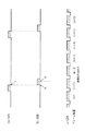
図11(a)〜(c)は、マトリクス型表示装置9のマトリクス型表示パネル22上で、左端から右端に向かって移動する太い縦線を示した図である。
なお、図10(c)に示した表示パネル22のフレーム周波数は、一般的には毎秒60フレーム程度であり、グラフィックスメモリ11からフレームメモリ21へのデータ転送の頻度の数倍である。また、画像データGD2のデータ転送は、マトリクス型表示パネル22へフレームメモリ21から読み出す画像データGD3とは非同期に行われる。図10(c)に示したように、フレームメモリ21から読み出された1フレーム毎の画像データGD3を、早い方から順に(n)フレーム目、(n+1)フレーム目、(n+2)フレーム目とすると、まず、(n)フレーム目の縦線100aの画像は、図11(a)のように縦に連続して表示される。
【0013】
次に、画像データGD2とGD3は同期していないので、図10(c)の(n+1)フレーム目のタイミングt2では、読み出される画像データ信号GD3に、書込む画像データ信号GD2が追いつき、その後で追い越してしまう。すると、図11(b)に示したように、(n+1)フレーム目の縦線100bの画像は、垂直走査方向のタイミングt2から下が、新たに書込みまれた縦線101aとなり、縦線が連続しないで段差ができてしまう。この縦線の段差は、図11(c)に示した(n+2)フレーム目では、新たに書込みまれた縦線101bのみとなり、段差は無くなる。
【0014】
このように、図9に示した従来のマトリクス型表示装置9では、マトリクス型表示パネル22のフレーム周期と非同期に画像データGD2がグラフィックスメモリ11からフレームメモリ21に転送されるため、表示パネル22に表示される画像の1フレームの途中で次の1フレームの画像に切り替わる事態が発生する。
【0015】
このような事態は、マトリクス型表示パネル22として応答速度の遅い従来からのSTN液晶パネルを使用している場合にも発生する。しかし、従来のSTN液晶パネルの場合には、液晶の応答速度が表示パネルにおける1フレームの画像データ転送速度と比較して十分大きいため、動きのある動画像を表示させようとして1フレーム毎の映像データを転送しても液晶側の応答が間に合わず十分な表示ができなくなるという問題があり、そのため、液晶表示パネルの1フレームを表示する途中で次の画像が転送されることにより画像に縦の段差が発生しても、その前に表示できなくなっていることが多かったため、比較的目に付きにくく放置されていた。
【0016】
【発明が解決しようとする課題】
しかしながら、上記したように動画像を表示させるために、例えば、アクティブマトリクス型液晶パネル、高速応答STNパネル、あるいは、有機ELパネル等の応答速度の比較的速い表示パネルを携帯電話装置へ使用した場合には、図11(b)に示した横方向に動きのある画像データの映像について、応答性の点では問題無くなることから、1フレームの途中で次の画像に切り替わり、画像に縦の段差が発生するという問題が顕在化してしまう。その結果、表示される動画像の品位が著しく損われてしまう。従って、応答速度が比較的速い表示パネルを携帯電話等に使用する場合には、画像に縦の段差が発生するという問題が放置できない問題となる。
【0017】
本発明は、以上のような問題点を解決するためになされたものであって、動画像の品位を損なわず、なめらかな動画像を表示できる携帯情報端末装置用のマトリクス型表示装置を提供することを目的とする。
【0018】
【課題を解決するための手段】
この発明に係るマトリクス型表示装置は、
外部から入力される画像データをフレーム単位で記憶可能なグラフィックスメモリと、
外部から入力される画像データのフレーム毎の当該グラフィックスメモリへの書込完了時に書込完了信号を出力するメモリデータ書込制御回路と、
書込完了信号とフレーム同期信号とに基づいて、読出開始信号を出力する同期化回路と、
読出開始信号に基づいて、グラフィックスメモリに記憶された画像データをフレーム単位で読み出すデータ読出制御回路と、
グラフィックスメモリから読み出された画像データをフレーム単位で記憶するフレームメモリと、
自回路内で発生するクロック信号に基づいて、前記フレームメモリに記憶された画像データを読み出すと共に、複数の信号線を駆動するための制御信号を出力し、かつ、フレーム同期信号を出力する信号電極駆動回路と、
フレーム同期信号に基づいて、複数の走査線を駆動するための制御信号を出力する走査電極駆動回路と、
複数の信号線と、信号線と直交する方向に配線された複数の走査線との交点に画素部が設けられた表示パネルと
を備えることとしたものである。
【0028】
【発明の実施の形態】
以下、本発明にかかわるマトリクス型表示装置を、その実施の一形態を示す図面に基づき具体的に説明する。なお、以下の各図において、図9〜図11を用いて上記に説明した従来のマトリクス型表示装置9と同一の機能を有するものには、同一符号を付して示して重複する説明を省略する。
【0029】
実施の形態1.
図1は本発明の実施の形態1であるマトリクス型表示装置を示す図である。
図1のマトリクス型表示装置1と図9のマトリクス型表示装置9との主な相違点は、表示パネルモジュール部20内の信号電極駆動回路23から出力されるフレーム同期信号FSに同期させて、読み出し開始信号をデータ読出制御回路13に対して出力する同期化回路14を、入力制御部10内に備える点である。また、上記した同期化回路14の追加に伴い、データ書込み制御部12は、同期化回路14に書込完了信号WEを出力できるようになっており、信号電極駆動回路23は、フレーム同期信号を走査電極駆動回路24に出力すると共に同期化回路14にも出力できるようになっている。他の構成に付いては、図11に示した従来のマトリクス型表示装置9と同一であるので説明を省略する。
【0030】
図2は、図1の表示パネルモジュール部20内の信号電極駆動回路23の内部構成を示すブロック図である。
信号電極駆動回路23内において、41は、マトリクス表示パネル22に画像を表示させるための基準となるクロック信号(基準信号)SSを発生する発振回路である。42は、基準信号SSに基づいて、フレームメモリ21に読み出し制御信号RCを出力し、操作電極駆動回路24にフレーム同期信号FSおよびライン同期信号LSを出力し、後述するデコーダ回路43に画像データをデコードするための同期信号を出力する表示制御回路である。なお、フレーム同期信号FSについては、表示制御回路42から同期化回路14へも出力される。43は、表示制御回路42からの同期信号および画像データのコーディングルールに基づいてコード化された画像データGD3を画像表示可能な画像データに変換(デコード)するデコーダ回路である。44は、デコードされた画像データGD3に基づいて、マトリクス型表示パネル22の各信号電極に電圧を印加して駆動する表示パネル駆動回路である。
【0031】
図3は、図1のフレームメモリ21のアドレス構成を示す図である。
図3に示すように、マトリクス型表示装置1における水平ドット数N/垂直ライン数Mのフレームメモリ21においては、データ読出制御回路13が、グラフィックスメモリ11から読み出された1画面分の画像データを、フレームメモリ21のアドレス0からアドレスN×M−1まで順次書きこむ。さらに詳しくは、データ読出制御回路13が、最初の1ライン目の画像データをアドレス0からアドレスN−1まで書込みみ、次に、2ライン目の画像データをアドレスNからアドレスN×2−1まで書き込む。同様にして各ラインの画像データを書込みみ、最終ラインであるMライン目の画像データをアドレスN×(M−1)からアドレスN×M−1まで書き込んで1画面の書込みを終了する。
【0032】
なお、フレームメモリ21に一旦書き込まれてから読み出されるデータとしては、画像データに限らず、例えば、文字等を構成するデータでも良い。また、フレームメモリ21のデータ転送速度としては、IMT−2000規格対応の動画対応の携帯電話においては、データ通信速度等の制約により当面は毎秒15画面程度までの転送速度が想定されている。しかし、この転送速度に付いては、将来的には毎秒30画面程度まで上がっていくことが予想される。
【0033】
次に、マトリクス型表示装置1の動作について、図1〜3に加えて、図4のタイミングチャートを参照して以下に説明する。
通信機能等により外部からマトリクス型表示装置1の入力制御部10に入力した画像データGD1は、データ書込制御回路12により制御されて一旦グラフィックスメモリ11に記憶される。図4(a)に示したように、グラフィックスメモリ11への画像データGD1の記憶処理がタイミングt1で終了すると、図4(b)に示したように、t1のタイミングで、データ書込制御回路12から書込完了信号WEが同期化回路14に送出される。この書込完了信号WEが入力することにより、同期化回路14はリセットされて、以下の動作を実施する。
【0034】
同期化回路14では、図4(d)に示したフレーム同期信号FSであって、書込完了信号WEを受信した後の最初のものが入力されるのを待ち、その入力するタイミングt3に同期させて読み出し開始信号RKをデータ読出制御回路13に送出する。すると、データ読出制御回路13によってグラフィックメモリ11に一時記憶された画像データGD1は、タイミングt3で読み出され、画像データGD2としてフレームメモリ21に転送される。
【0035】
一方、表示パネルモジュール部20では、信号電極駆動回路23により、図4(e)に示したように、発振回路41によって発生された基準信号41(クロック信号)に基づくリフレッシュサイクルで、フレームメモリ21に記憶された画像データGD2が、画像データGD3として周期的に読み出されて、信号電極駆動回路23に入力される。フレームメモリ21から読み出された1フレーム毎の画像データGD3を、早い方から順に(n)フレーム目、(n+1)フレーム目、(n+2)フレーム目、以後同様に数値nを漸増させた順番とする。なお、nは正の整数である。
【0036】
信号電極駆動回路23内の表示制御回路42では、基準信号41に基づいて、フレームメモリ21に向けて読み出し制御信号RCを生成して送出し、デコーダ回路43にデコード用の同期信号を送出すると共に、フレーム同期信号FSおよびライン同期信号LSを生成して走査電極駆動回路24に送出する。デコーダ回路43は、表示制御回路42からの同期信号と画像データのコーディングルールに基づいて、入力した画像データGD3をマトリクス型表示パネル22で画像表示可能な画像データにデコードする。表示パネル駆動回路44は、デコードされた画像データからマトリクス型表示パネル22の各信号電極に対する制御信号を生成して送出する。走査電極駆動回路24では、フレーム同期信号FSおよびライン同期信号LSに基づいて、マトリクス型表示パネル22の走査電極に対する制御信号を生成して送出する。
【0037】
図4(c)および図4(e)を参照してわかるように、フレームメモリ21に記憶された(n+2)番目の画像データを読出すためのフレーム同期信号FSの送出タイミングt3に同期させて、データ読出制御回路13によりグラフィックスメモリ11からフレームメモリ21への次の画像データGD2の転送が行われる。また、画像データGD3は、フレーム同期信号FSから遅延時間DT1だけ遅れて出力される。従って、フレームメモリ21に記憶された(n+2)番目の画像データをGD3として読出す時には、新規に転送されて記憶された画像データGD2をGD3として読み出すことになり、画像データ読み出し中に新規に転送された画像データに切り替わることが無くなる。
【0038】
図5(a)〜(c)は、マトリクス型表示装置1のマトリクス型表示パネル22上で、左端から右端に向かって移動する太い縦線を示した図である。
図4(e)に示したように、フレームメモリ21から読み出された1フレーム毎の画像データGD3を、早い方から順に(n)フレーム目、(n+1)フレーム目、(n+2)フレーム目とすると、まず、(n)フレーム目の縦線100aの画像は、図5(a)のように縦に連続して表示される。
【0039】
次に、画像データGD2はフレーム同期信号FSと同期し、画像データGD3の(n+2)番目の画像データはフレーム同期信号FSにDT1だけ遅延したタイミングt4に同期して読み出される。また、フレーム同期信号FSのタイミングt3は、画像データGD3の出力が開始されるタイミングt4よりDT1だけ先行するだけであるので、図4(e)の(n+1)フレーム目では、転送中の画像データGD2に切り替わることはない。従って、図5(b)に示したように、(n+1)フレーム目の縦線100bの画像は、図5(a)に示した(n)フレーム目の縦線100aの画像と同様になり、縦線が連続して段差ができなくなる。次の、図5(c)に示した(n+2)フレーム目は、新たに書込みまれた縦線101bのみが表示され、従来と同様に段差は発生しない。
【0040】
このように、本実施の形態1のマトリクス型表示装置1では、マトリクス型表示パネル22のフレーム周期と同期されて画像データGD2がグラフィックスメモリ11からフレームメモリ21に転送されるため、フレームメモリ21への画像データGD2の転送処理と、フレームメモリ21から信号電極駆動回路23への画像データGD3の読み出し処理が同一アドレスに一致しないようになり、マトリクス型表示パネル22に表示される画像の1フレームの途中で次の1フレームの画像に切り替わらなくなるようにデータ転送を制御することから、動画像を表示させたときに、1画面の上部と下部の画像内容が時間的にずれる事態が発生しなくなり、なめらかな映像を表示することができる。
【0041】
実施の形態2.
実施の形態1では、グラフィックスメモリ11からフレームメモリ21への画像データGD2の転送開始タイミングを、フレーム同期信号FSに同期させることにより、フレームメモリ21から読み出される画像データGD3の途中で画像が新規書込みされた画像に切り替わらないようにしたが、信号電極駆動回路23により、フレーム同期信号FSに基づいてフレームメモリ21から画像データGD3を読み出す際には遅延時間DT1が発生する。例えば、その遅延時間DT1が長くなると、図4(e)の(n+1)フレーム目の画像データGD3の読み出し終了タイミングと、画像データGD2の転送終了タイミングが近づき、画像データGD2の転送終了タイミングが画像データGD3の読み出し終了タイミングを追い越してしまう場合には、再び、マトリクス型表示パネル22に表示される画像の1フレームの途中で、次の1フレームの画像に切り替わる可能性が出てくる。
そこで、以下に説明する実施の形態2では、マトリクス型表示装置のフレーム同期信号FSから画像データGD3の読み出しまでの遅延時間DT1が長くなりすぎないようにした。
【0042】
図6は本発明の実施の形態2のマトリクス型表示装置の構成を示すブロック図である。
図6のマトリクス型表示装置2と図1のマトリクス型表示装置1との主な相違点は、信号電極駆動回路23から送出されたフレーム同期信号FSを、任意の1フレームの画像データGD3の読み出し終了タイミングt5に同期するように所定時間だけ遅延させて読み出し同期信号RSとして出力する遅延回路30を備える点である。他の構成に付いては、図1に示した実施の形態1のマトリクス型表示装置1と同一であるので説明を省略する。
【0043】
次に、マトリクス型表示装置2の動作について、図6に加えて、図7のタイミングチャートを参照して以下に説明する。
図7(a)、(b)、(d)および(f)は、夫々図4(a)、(b)、(d)および(e)に対応する同信号であるので説明を省略する。図7(e)は、遅延回路30によりフレーム同期信号FSを、(n+1)フレームの画像データGD3の読み出し終了タイミングt5に同期するように所定時間DT2だけ遅延させた読み出し同期信号RSを示すものである。図7(c)は、読み出し同期信号RSに同期させて転送される画像データGD2を示すものである。
【0044】
フレーム同期信号FSから(n+2)フレームの画像データGD3の読み出し開始タイミングt4までの遅延時間DT1が長くなりすぎることをなくすために、フレーム同期信号FSを直接に同期化回路14に入力させずに、遅延回路30で遅延させた読み出し同期信号RSを同期化回路14に入力させるようにしたので、遅延時間DT1が遅延回路30の遅延時間DT2分だけ短縮された遅延時間DT3となる。また、読み出し同期信号RSは、(n+1)フレームの画像データGD3の読み出し終了タイミングt5に同期して発生されるので、マトリクス型表示パネル22に表示される画像の1フレームの途中で次の1フレームの画像に切り替わる事態を無くすことができる。
【0045】
このように本実施の形態2では、フレーム同期信号FSを遅延させた読み出し同期信号RSを出力する遅延回路30を同期化回路14のフレーム同期信号入力部の前段に追加することにより、例えば、30〜50mSec程度の応答速度であるTFT等のアクティブマトリクス型液晶パネル、70〜80mSec程度の応答速度である高速応答型のSTN液晶パネル、数μSec程度の応答速度である有機ELパネルの夫々に対するように異なる応答速度を有するマトリクス型表示パネルの夫々に対して、遅延時間が長くなりすぎない最適な遅延量を遅延回路30で設定して読み出し同期信号RSとして出力できるようにしたので、マトリクス型表示パネルの種類を問わず、信号電極駆動回路23からのフレーム同期信号FSが画像データGD2の転送タイミングとして適切でない場合にも、なめらかな動画像を表示させることができる。
【0046】
実施の形態3.
実施の形態2では、フレーム同期信号FSが入力され、その信号FSを画像データGD3の読み出し終了タイミングt5に同期するように最適に遅延させた読み出し同期信号RSとして出力する遅延回路30を、同期化回路14のフレーム同期信号入力部の前段に追加することにより、マトリクス型表示パネル22に表示される画像の1フレームの途中で次の1フレームの画像に切り替わる事態を無くしていたが、遅延回路30で用いられるクロック信号は、信号電極駆動回路23内部のクロック信号(基準信号SS)と同一であるとは限らなかった。
基準信号SSと遅延回路30で用いられるクロック信号とが異なる場合には、夫々の発振回路のばらつきにより、読み出し同期信号RSを最適な遅延量に設定できない場合があった。
そこで、以下に説明する実施の形態3では、読み出し同期信号RSが信号電極駆動回路23内部のクロック信号(基準信号SS)と同期するようにして、発振回路のばらつきの影響を受けないようにした。
【0047】
図8は、本発明の実施の形態3のマトリクス型表示装置の構成を示すブロック図である。
図8のマトリクス型表示装置3と図2のマトリクス型表示装置2との主な相違点は、遅延回路31に信号電極駆動回路23から送出されたフレーム同期信号FSに加えてライン同期信号LSが入力される点である。本実施の形態2では、ライン同期信号LSを遅延回路31のクロック信号として利用するようにした。他の構成に付いては、図6に示した実施の形態2のマトリクス型表示装置2と同一であるので説明を省略する。
【0048】
次に、マトリクス型表示装置3の動作について、図8に加えて、実施の形態2の図7のタイミングチャートを参照して以下に説明する。
基準信号SSと遅延回路30で用いられるクロック信号とが異なる場合には、例えば、図7(e)の読み出し同期信号RSが、図7(f)の(n+1)フレームの画像データGD3の読み出し終了タイミングt5と一致しなくなる。すると、読み出し同期信号RSに同期させて転送される画像データGD2も画像データGD3の読み出し終了タイミングt5と一致しなくなるので、再び、マトリクス型表示パネル22に表示される画像の1フレームの途中で次の1フレームの画像に切り替わる事態が発生する可能性が出てくる。
【0049】
ところで、信号電極駆動回路23から送出されたフレーム同期信号FSとライン同期信号LSは、図2に示したように同じ発振回路41からの基準信号SSに基づいて生成されるので、発振回路毎にばらつきが発生しても、フレーム同期信号FSとライン同期信号LS間の同期がばらつくことはない。
【0050】
そのため、本実施の形態3では、図8に示したようにライン同期信号LSを遅延回路31のクロック信号として入力するように構成している。こうすることにより、予め設定されたライン同期信号LSのパルス数だけフレーム同期信号FSを遅延させた信号を、読み出し同期信号RSとして遅延回路31から出力できるようになる。この場合には、読み出し同期信号RSがフレーム同期信号FSから遅延する量はばらつかないので、(n+1)フレームの画像データGD3の読み出し終了タイミングt5と、読み出し同期信号RSに同期させて転送される画像データGD2とを確実に同期させることができる。従って、マトリクス型表示パネル22に表示される画像の1フレームの途中で次の1フレームの画像に切り替わる事態を無くすことができる。
【0051】
このように本実施の形態3では、遅延回路31にフレーム同期信号FSに加えてライン同期信号LSを入力させ、ライン同期信号LSをクロックとしてフレーム同期信号FSを遅延させることにより読み出し同期信号RSを出力するようにし、発振回路等のばらつきにより読み出し同期信号RSの発生タイミングがばらつかず、最適な遅延量を有する読み出し同期信号RSを出力することができるようにして、フレーム同期信号FSから一定の位相量だけ遅延させた最適な遅延量の読み出し同期信号RSを設定できるようにしたので、例えば、上記したアクティブマトリクス型液晶パネル、高速応答型のSTN液晶パネル、有機ELパネル等のマトリクス型表示パネルの種類を問わず、発振回路の周波数ドリフト等が発生しやすい状況であっても発振回路のばらつきに影響されず、安定したなめらかな動画像を表示させることができる。
【0052】
また、上記の各実施形態のマトリクス型表示パネルが液晶パネルである場合には、透過型、反射型、あるいは、反射半透過型に分類することができる。透過型の液晶パネルは、画像表示内容を視認するためにバックライト等の内部照明が必要であり、バックライトには電力が必要となるので、低消費電力が要望される携帯電話等の携帯情報端末装置では使用することが難しい。それに対して反射型は、背面側の全面に反射板を設けることにより外部からの光の反射光により画像表示内容を視認できることから、バックライトの電力が不要であるので、低消費電力が要望される携帯電話等の携帯情報端末装置に向いている。また、反射半透過型は、背面側に網点状等の半透過型の反射板を設けることにより外部からの光の反射光と内部照明の双方により画像表示内容を視認できることから、反射型と同様にバックライトの電力が不要であり、さらに、外部が暗い場合のみ内部照明を用いて視認することができるので、低消費電力が要望される携帯電話等の携帯情報端末装置に向いていることに加え、暗い場所での視認性も向上するので使い勝手をよくすることができる。
【0053】
また、マトリクス型表示パネルとしてアクティブマトリクス型の液晶表示パネルを用いた場合、従来の応答速度が遅いSTN型の液晶表示パネルに比べて、応答速度と周囲に対する表示部のコントラストが向上するので、動きの激しい動画像あるいは高速に移動する動画像を表示する場合であっても、安定したなめらかな動画像を表示させることができることに加えて、視認性を向上させることができる。
【0054】
また、マトリクス型表示パネルとして高速応答型STN液晶表示パネルを用いた場合、従来の応答速度が遅いSTN型の液晶表示パネルに比べて、応答速度が向上するので、低消費電力と低コストを維持したままで、動きの激しい動画像あるいは高速に移動する動画像を表示する場合であっても、安定したなめらかな動画像を表示させることができる。
【0055】
また、マトリクス型表示パネルとして有機蛍光表示パネルを用いた場合、アクティブマトリクス型の液晶表示パネルと同様に、従来の応答速度が遅いSTN型の液晶表示パネルに比べて、応答速度が向上する。また、有機蛍光表示パネルの場合には、表示部自体が発光することにより周囲に対する表示部のコントラストが向上するので、安定したなめらかな動画像を表示させることができることに加えて、視認性を液晶よりもさらに向上させることができので画質をさらに向上させ、バックライトが不要であるので薄型化することができる。
【0056】
また、マトリクス型表示パネルとしてアクティブマトリクス型の有機蛍光表示パネルを用いた場合、動きの激しい動画像あるいは高速に移動する動画像を表示する場合であっても、安定したなめらかな動画像を表示させることができ、視認性を液晶よりもさらに向上させることができるので画質をさらに向上させ、薄型化することができる。
【0057】
【発明の効果】
本発明は、以上説明したように構成されているので、以下に示すような効果を奏する。
すなわち、マトリクス型表示パネルのフレーム周期と同期されて画像データがグラフィックスメモリからフレームメモリに転送されるため、フレームメモリへの画像データの転送処理と、フレームメモリから信号電極駆動回路への画像データの読み出し処理が同一アドレスに一致しないようになり、マトリクス型表示パネルに表示される画像の1フレームの途中で次の1フレームの画像に切り替わらなくなるようにデータ転送を制御するので、動画像を表示させたときに、1画面の上部と下部の画像内容が時間的にずれる事態が発生しなくなり、なめらかな映像を表示することができる。
【図面の簡単な説明】
【図1】本発明の実施の形態1のマトリクス型表示装置の構成を示すブロック図である。
【図2】図1の信号電極駆動回路の内部構成を示すブロック図である。
【図3】図1のフレームメモリのアドレス構成を示す図である。
【図4】(a)〜(e)は図1のマトリクス型表示装置のタイミングチャートである。
【図5】(a)〜(c)はマトリクス型表示パネル上で左端から右端に向かって移動する太い縦線を示した図である。
【図6】本発明の実施の形態2のマトリクス型表示装置の構成を示すブロック図である。
【図7】(a)〜(f)は図6のマトリクス型表示装置のタイミングチャートである。
【図8】本発明の実施の形態3のマトリクス型表示装置の構成を示すブロック図である。
【図9】従来のフレームメモリ内蔵のマトリクス型表示装置の構成を示すブロック図である。
【図10】(a)〜(c)は従来のマトリクス型表示装置のタイミングチャートである。
【図11】(a)〜(c)は従来のマトリクス型表示パネル上で左端から右端に向かって移動する太い縦線を示した図である。
【符号の説明】
1 マトリクス型表示装置、 10 入力制御部、 11 グラフィックスメモリ、 12 データ書込制御回路、 13 データ読出制御回路、 14 同期化回路、 20 表示パネルモジュール、 21 フレームメモリ、 22 マトリクス型表示パネル、 23 信号電極駆動回路、 24 走査電極駆動回路、 GD1、GD2、GD3 画像データ、 FS フレーム同期信号、 LS ライン同期信号、 RC 読み出し制御信号、 RK 読み出し開始信号、
WE 書込完了信号。[0001]
BACKGROUND OF THE INVENTION
The present invention relates to a display device for displaying an image using a display panel such as a matrix type liquid crystal panel or a matrix type fluorescent display panel in which pixel portions are provided at intersections arranged in a matrix, and in particular, a moving image. The present invention relates to a matrix type display device used in a display unit of a portable information terminal device such as a mobile phone device that displays a message.
[0002]
[Prior art]
2. Description of the Related Art Conventionally, display devices using a matrix type liquid crystal or the like have been used for portable information processing devices such as mobile phone devices and portable information terminal devices.
For example, in recent mobile phones, as a basic requirement, it is required to secure a battery driving time of several hundred hours with a so-called standby screen displayed. For this reason, the matrix display device used in a mobile phone does not require image data transfer during still image display and reduces power consumption. In addition, a frame memory is often built in a circuit for driving a liquid crystal display panel. In other words, at the time of still image display, data is transferred to a circuit for driving a liquid crystal display panel so that power is not consumed, and a low power consumption liquid crystal matrix type display device configured as such Has been used in many mobile phones in recent years.
[0003]
As a conventional liquid crystal display panel for a mobile phone, a STN liquid crystal panel having a built-in frame memory as described above and further reducing power consumption and cost is often used. However, in the future, it is expected that a video delivery function corresponding to the IMT-2000 standard will start and a TV phone function will be added. In that case, it is necessary to display a moving image, and the conventional STN (super twisted birefringence type) liquid crystal panel is insufficient in response speed, so it is expected to be switched to a display panel for a mobile phone that supports moving image display. . Specifically, it is expected that active matrix liquid crystal panels such as TFT (Thin Film Transistor) liquid crystal panels and MIM (Metal Insulator Metal) liquid crystal panels with high response speed and high image quality are mainly used.
[0004]
In general, an active matrix liquid crystal panel that is expected to be used in the future is not as low in power consumption as an STN liquid crystal panel used in the past. In recent years, however, mobile phones that have been reduced in power consumption to a usable level have been developed.
[0005]
On the other hand, a high-speed response STN liquid crystal panel that can display a moving image by increasing the response speed has been developed for an STN liquid crystal panel that is assumed to have a relatively low response speed and will be used in the future.
In addition, the organic EL display panel that displays the pixel part itself with a method of emitting light is much faster than the liquid crystal panel and is a self-luminous display panel. Therefore, there is no need for illumination such as a backlight or a front light. The power consumption is not so much. Therefore, the organic EL display panel can be reduced in thickness and weight by illumination such as a backlight, and thus is considered suitable as a display panel for a mobile phone.
[0006]
The general response speed of each display panel described above is about 300 to 500 mSec for STN liquid crystal panels conventionally used in mobile phones, and about 30 to 50 mSec for active matrix liquid crystal panels such as TFTs. The high-speed response type STN liquid crystal panel is about 70 to 80 mSec, and the organic EL panel is about several μSec.
[0007]
FIG. 9 is a block diagram showing the configuration of a conventional matrix display device with a built-in frame memory.
In the matrix type display device 9 shown in FIG. 9,
The
[0008]
The display
[0009]
The image data that is input to the matrix display device 9 from the outside and written to the
[0010]
The operation of the matrix display device 9 will be described below with reference to the timing chart of image data in FIG. 10 in addition to FIG.
Image data GD1 externally input to the
[0011]
On the other hand, in the display
[0012]
11A to 11C are diagrams showing thick vertical lines moving from the left end toward the right end on the
The frame frequency of the
[0013]
Next, since the image data GD2 and GD3 are not synchronized, the image data signal GD2 to be written catches up with the image data signal GD3 to be read at the timing t2 of the (n + 1) frame in FIG. Overtake. Then, as shown in FIG. 11B, the image of the
[0014]
As described above, in the conventional matrix display device 9 shown in FIG. 9, the image data GD2 is transferred from the
[0015]
Such a situation also occurs when a conventional STN liquid crystal panel having a slow response speed is used as the matrix
[0016]
[Problems to be solved by the invention]
However, in order to display a moving image as described above, for example, when a display panel having a relatively high response speed such as an active matrix liquid crystal panel, a high-speed response STN panel, or an organic EL panel is used for a mobile phone device. 11 (b), there is no problem in terms of responsiveness with respect to the video of the image data moving in the horizontal direction, so that the next image is switched in the middle of one frame, and there is a vertical step in the image. The problem of occurring becomes obvious. As a result, the quality of the displayed moving image is significantly impaired. Therefore, when a display panel having a relatively high response speed is used for a mobile phone or the like, the problem that a vertical step occurs in the image cannot be left unattended.
[0017]
The present invention has been made to solve the above problems, and provides a matrix type display device for a portable information terminal device that can display a smooth moving image without deteriorating the quality of the moving image. For the purpose.
[0018]
[Means for Solving the Problems]
A matrix type display device according to the present invention provides:
A graphics memory capable of storing image data input from outside in units of frames;
A memory data write control circuit for outputting a write completion signal upon completion of writing to the graphics memory for each frame of image data input from the outside;
A synchronization circuit that outputs a read start signal based on the write completion signal and the frame synchronization signal;
Based on the read start signal, the image data stored in the graphics memory In frames A data read control circuit for reading; and
A frame memory for storing image data read from the graphics memory in units of frames;
A signal electrode that reads out image data stored in the frame memory based on a clock signal generated in its own circuit, outputs a control signal for driving a plurality of signal lines, and outputs a frame synchronization signal A drive circuit;
A scan electrode drive circuit that outputs a control signal for driving a plurality of scan lines based on the frame synchronization signal;
A display panel in which a pixel portion is provided at an intersection of a plurality of signal lines and a plurality of scanning lines wired in a direction orthogonal to the signal lines;
It is supposed to be equipped with.
[0028]
DETAILED DESCRIPTION OF THE INVENTION
Hereinafter, a matrix display device according to the present invention will be specifically described with reference to the drawings showing an embodiment thereof. In addition, in each figure below, what has the same function as the conventional matrix type display apparatus 9 demonstrated above using FIGS. 9-11 is attached | subjected, and the overlapping description is abbreviate | omitted. To do.
[0029]
FIG. 1 is a diagram showing a matrix display device according to
The main difference between the matrix
[0030]
FIG. 2 is a block diagram showing an internal configuration of the signal
In the signal
[0031]
FIG. 3 is a diagram showing an address configuration of the
As shown in FIG. 3, in the
[0032]
Note that the data read once written in the
[0033]
Next, the operation of the
Image data GD1 externally input to the
[0034]
The
[0035]
On the other hand, in the display
[0036]
The
[0037]
As can be seen with reference to FIG. 4C and FIG. 4E, in synchronization with the transmission timing t3 of the frame synchronization signal FS for reading the (n + 2) -th image data stored in the
[0038]
FIGS. 5A to 5C are diagrams showing thick vertical lines that move from the left end toward the right end on the
As shown in FIG. 4 (e), the image data GD3 for each frame read from the
[0039]
Next, the image data GD2 is synchronized with the frame synchronization signal FS, and the (n + 2) th image data of the image data GD3 is read in synchronization with the timing t4 delayed by DT1 from the frame synchronization signal FS. Further, since the timing t3 of the frame synchronization signal FS only precedes the timing t4 when the output of the image data GD3 is started by DT1, the image data being transferred is transmitted at the (n + 1) th frame in FIG. There is no switch to GD2. Therefore, as shown in FIG. 5B, the image of the
[0040]
As described above, in the matrix
[0041]
In the first embodiment, by synchronizing the transfer start timing of the image data GD2 from the
Therefore, in the second embodiment described below, the delay time DT1 from the frame synchronization signal FS of the matrix display device to the reading of the image data GD3 is prevented from becoming too long.
[0042]
FIG. 6 is a block diagram showing the configuration of the matrix type display device according to the second embodiment of the present invention.
The main difference between the matrix
[0043]
Next, the operation of the
7 (a), (b), (d), and (f) are the same signals corresponding to FIGS. 4 (a), (b), (d), and (e), respectively, and thus description thereof is omitted. FIG. 7E shows a read synchronization signal RS obtained by delaying the frame synchronization signal FS by the
[0044]
In order to prevent the delay time DT1 from the frame synchronization signal FS to the read start timing t4 of the image data GD3 of the (n + 2) frame, the frame synchronization signal FS is not directly input to the
[0045]
As described above, in the second embodiment, the
[0046]
In the second embodiment, the frame synchronization signal FS is input, and the
When the reference signal SS and the clock signal used in the
Therefore, in the third embodiment described below, the readout synchronization signal RS is synchronized with the clock signal (reference signal SS) in the signal
[0047]
FIG. 8 is a block diagram showing the configuration of the matrix type display device according to the third embodiment of the present invention.
The main difference between the
[0048]
Next, the operation of the
When the reference signal SS and the clock signal used in the
[0049]
Incidentally, the frame synchronization signal FS and the line synchronization signal LS sent from the signal
[0050]
Therefore, in the third embodiment, the line synchronization signal LS is input as a clock signal of the
[0051]
As described above, in the third embodiment, the line synchronization signal LS is input to the
[0052]
Further, when the matrix type display panel of each of the above embodiments is a liquid crystal panel, it can be classified into a transmission type, a reflection type, or a reflection transflective type. The transmissive liquid crystal panel requires internal lighting such as a backlight to visually recognize the image display contents. Since the backlight requires power, portable information such as a mobile phone that requires low power consumption is required. It is difficult to use with a terminal device. On the other hand, the reflective type is provided with a reflector on the entire back surface, so that the image display contents can be visually recognized by the reflected light from the outside. It is suitable for portable information terminal devices such as mobile phones. In addition, the reflective transflective type is provided with a semi-transmissive reflector such as a halftone dot on the back side so that the image display content can be visually recognized by both reflected light from the outside and internal illumination. Similarly, it does not require backlight power, and can be viewed using internal lighting only when the outside is dark, so it is suitable for portable information terminal devices such as mobile phones that require low power consumption. In addition, the visibility in dark places is improved, so it is easy to use.
[0053]
Also, when an active matrix type liquid crystal display panel is used as the matrix type display panel, the response speed and the contrast of the display unit with respect to the surroundings are improved as compared with the conventional STN type liquid crystal display panel having a low response speed. Even when displaying a moving image that is intense or moving at high speed, in addition to being able to display a stable and smooth moving image, it is possible to improve visibility.
[0054]
In addition, when a high-speed response type STN liquid crystal display panel is used as the matrix type display panel, the response speed is improved as compared with the conventional STN type liquid crystal display panel having a low response speed, so that low power consumption and low cost are maintained. Even when a moving image with intense movement or a moving image that moves at high speed is displayed as it is, a stable and smooth moving image can be displayed.
[0055]
In addition, when an organic fluorescent display panel is used as the matrix type display panel, the response speed is improved as compared with the conventional STN type liquid crystal display panel having a low response speed, similar to the active matrix type liquid crystal display panel. In addition, in the case of an organic fluorescent display panel, the display unit itself emits light, thereby improving the contrast of the display unit with respect to the surroundings. In addition to being able to display a stable and smooth moving image, the visibility is liquid crystal Therefore, the image quality can be further improved, and the backlight can be reduced, so that the thickness can be reduced.
[0056]
In addition, when an active matrix organic fluorescent display panel is used as the matrix display panel, a stable and smooth moving image is displayed even when a moving image with high motion or a moving image moving at high speed is displayed. In addition, since the visibility can be further improved as compared with the liquid crystal, the image quality can be further improved and the thickness can be reduced.
[0057]
【The invention's effect】
Since the present invention is configured as described above, the following effects can be obtained.
That is, Since the image data is transferred from the graphics memory to the frame memory in synchronization with the frame period of the matrix display panel, the image data is transferred to the frame memory and the image data is read from the frame memory to the signal electrode drive circuit. Data transfer is controlled so that processing does not match the same address, and the image is not switched to the next one frame in the middle of one frame of the image displayed on the matrix display panel. , Dynamic When an image is displayed, a situation in which the image contents at the top and bottom of one screen are not shifted in time does not occur, and a smooth video can be displayed.
[Brief description of the drawings]
FIG. 1 is a block diagram illustrating a configuration of a matrix display device according to a first embodiment of the present invention.
2 is a block diagram showing an internal configuration of a signal electrode drive circuit of FIG. 1. FIG.
FIG. 3 is a diagram illustrating an address configuration of the frame memory of FIG. 1;
4A to 4E are timing charts of the matrix display device of FIG.
FIGS. 5A to 5C are diagrams showing thick vertical lines that move from the left end toward the right end on the matrix type display panel; FIGS.
FIG. 6 is a block diagram showing a configuration of a matrix display device according to a second embodiment of the present invention.
7A to 7F are timing charts of the matrix display device of FIG.
FIG. 8 is a block diagram showing a configuration of a matrix display device according to a third embodiment of the present invention.
FIG. 9 is a block diagram showing the configuration of a conventional matrix display device with a built-in frame memory.
FIGS. 10A to 10C are timing charts of a conventional matrix display device.
FIGS. 11A to 11C are diagrams showing thick vertical lines moving from the left end toward the right end on a conventional matrix display panel. FIGS.
[Explanation of symbols]
DESCRIPTION OF
WE Write complete signal.
Claims (7)
前記外部から入力される画像データのフレーム毎の当該グラフィックスメモリへの書込完了時に書込完了信号を出力するメモリデータ書込制御回路と、
前記書込完了信号とフレーム同期信号とに基づいて、読出開始信号を出力する同期化回路と、
前記読出開始信号に基づいて、前記グラフィックスメモリに記憶された画像データをフレーム単位で読み出すデータ読出制御回路と、
前記グラフィックスメモリから読み出された画像データをフレーム単位で記憶するフレームメモリと、
自回路内で発生するクロック信号に基づいて、前記フレームメモリに記憶された画像データを読み出すと共に、複数の信号線を駆動するための制御信号を出力し、かつ、前記フレーム同期信号を出力する信号電極駆動回路と、
前記フレーム同期信号に基づいて、複数の走査線を駆動するための制御信号を出力する走査電極駆動回路と、
前記複数の信号線と、当該信号線と直交する方向に配線された上記複数の走査線との交点に画素部が設けられた表示パネルと
を備えるマトリクス型表示装置。A graphics memory capable of storing image data input from the outside in units of frames;
A memory data write control circuit that outputs a write completion signal when writing to the graphics memory for each frame of image data input from the outside is completed;
A synchronization circuit that outputs a read start signal based on the write completion signal and the frame synchronization signal;
A data read control circuit for reading out image data stored in the graphics memory in units of frames based on the read start signal;
A frame memory for storing image data read from the graphics memory in units of frames;
A signal that reads out image data stored in the frame memory based on a clock signal generated in its own circuit, outputs a control signal for driving a plurality of signal lines, and outputs the frame synchronization signal An electrode drive circuit;
A scan electrode drive circuit that outputs a control signal for driving a plurality of scan lines based on the frame synchronization signal;
A matrix display device comprising: a plurality of signal lines; and a display panel provided with a pixel portion at intersections of the plurality of scanning lines wired in a direction orthogonal to the signal lines.
同期化回路は、書込完了信号と当該読出同期信号とに基づいて、読出開始信号を出力する
ことを特徴とする請求項1に記載のマトリクス型表示装置。A delay circuit for outputting a read synchronization signal obtained by delaying the frame synchronization signal by a predetermined amount;
2. The matrix type display device according to claim 1, wherein the synchronization circuit outputs a read start signal based on the write completion signal and the read synchronization signal.
走査電極駆動回路は、当該ライン同期信号とフレーム同期信号とに基づいて、複数の走査線を駆動するための制御信号を出力し、
遅延回路は、前記ライン同期信号に基づいて、前記フレーム同期信号の遅延量を設定する
ことを特徴とする請求項2に記載のマトリクス型表示装置。The signal electrode drive circuit further outputs a line synchronization signal based on the clock signal generated in its own circuit,
The scan electrode drive circuit outputs a control signal for driving a plurality of scan lines based on the line synchronization signal and the frame synchronization signal,
3. The matrix display device according to claim 2, wherein the delay circuit sets a delay amount of the frame synchronization signal based on the line synchronization signal.
を特徴とする請求項1から3のいずれか1項に記載のマトリクス型表示装置。4. The synchronization circuit according to claim 1, wherein the synchronization circuit outputs a read start signal when a frame synchronization signal or a read synchronization signal is input for the first time after receiving a write completion signal. The matrix type display device described in 1.
書込完了信号出力後において、
初めてフレーム同期信号が入力されるタイミングから、
当該タイミングにおいてフレームメモリに記憶されていたフレームの画像データを、当該フレームメモリから読み出す処理の完了後のタイミングまでの期間であること
を特徴とする請求項2から4のいずれか1項に記載のマトリクス型表示装置。The delay amount of the read sync signal is
After the write completion signal is output,
From the timing when the frame sync signal is input for the first time,
Image data of a frame stored in the frame memory in the timing, according to claims 2, characterized in that a period from the timing after the completion of the process of reading from the frame memory in any one of 4 Matrix type display device.
上記外部から入力される画像データのフレーム毎の書込完了時に書込完了信号を出力する書込完了ステップと、
上記書込完了信号とフレーム同期信号とに基づいて、読出開始信号を出力する読出開始ステップと、
上記読出開始信号に基づいて、第1の記憶ステップで記憶された画像データをフレーム単位で読み出す読み出しステップと、
上記読み出しステップにて読み出された画像データをフレーム単位で記憶する第2の記憶ステップと、
クロック信号を発生し、当該クロック信号に基づいて、前記第2の記憶ステップで記憶された画像データを読み出すと共に、複数の信号線を駆動するための制御信号を出力し、かつ、上記フレーム同期信号を出力する信号電極駆動ステップと、
上記フレーム同期信号に基づいて、複数の走査線を駆動するための制御信号を出力する走査電極駆動ステップと、
前記複数の信号線と、当該信号線と直交する方向に配線された上記複数の走査線との交点に画素部が設けられた表示パネルに前記信号電極駆動ステップにて読み出された画像データを表示する表示ステップと
を備える画像データ表示方法。A first storage step of storing image data input from outside in units of frames;
A writing completion step of outputting a writing completion signal when writing of each frame of image data input from the outside is completed;
A read start step for outputting a read start signal based on the write completion signal and the frame synchronization signal;
A readout step of reading out the image data stored in the first storage step in units of frames based on the readout start signal;
A second storage step for storing the image data read in the reading step in units of frames;
Generating a clock signal, reading out the image data stored in the second storage step based on the clock signal, outputting a control signal for driving a plurality of signal lines, and the frame synchronization signal A signal electrode driving step for outputting
A scanning electrode driving step for outputting a control signal for driving a plurality of scanning lines based on the frame synchronization signal;
The image data read in the signal electrode driving step is displayed on a display panel in which a pixel portion is provided at an intersection of the plurality of signal lines and the plurality of scanning lines wired in a direction orthogonal to the signal lines. An image data display method comprising: a display step for displaying.
Priority Applications (5)
| Application Number | Priority Date | Filing Date | Title |
|---|---|---|---|
| JP2000293760A JP3611511B2 (en) | 2000-09-27 | 2000-09-27 | Matrix type display device, image data display method, and portable information terminal device |
| DE60105365T DE60105365T2 (en) | 2000-09-27 | 2001-09-24 | Matrix display device |
| EP01308110A EP1193671B1 (en) | 2000-09-27 | 2001-09-24 | Matrix-type display device |
| US09/962,166 US6700571B2 (en) | 2000-09-27 | 2001-09-26 | Matrix-type display device |
| CNB011411015A CN1157703C (en) | 2000-09-27 | 2001-09-27 | Array display device |
Applications Claiming Priority (1)
| Application Number | Priority Date | Filing Date | Title |
|---|---|---|---|
| JP2000293760A JP3611511B2 (en) | 2000-09-27 | 2000-09-27 | Matrix type display device, image data display method, and portable information terminal device |
Publications (3)
| Publication Number | Publication Date |
|---|---|
| JP2002108268A JP2002108268A (en) | 2002-04-10 |
| JP2002108268A5 JP2002108268A5 (en) | 2004-10-28 |
| JP3611511B2 true JP3611511B2 (en) | 2005-01-19 |
Family
ID=18776494
Family Applications (1)
| Application Number | Title | Priority Date | Filing Date |
|---|---|---|---|
| JP2000293760A Expired - Fee Related JP3611511B2 (en) | 2000-09-27 | 2000-09-27 | Matrix type display device, image data display method, and portable information terminal device |
Country Status (5)
| Country | Link |
|---|---|
| US (1) | US6700571B2 (en) |
| EP (1) | EP1193671B1 (en) |
| JP (1) | JP3611511B2 (en) |
| CN (1) | CN1157703C (en) |
| DE (1) | DE60105365T2 (en) |
Families Citing this family (24)
| Publication number | Priority date | Publication date | Assignee | Title |
|---|---|---|---|---|
| FI115802B (en) * | 2000-12-04 | 2005-07-15 | Nokia Corp | Refresh the photo frames on the memory display |
| US7009604B2 (en) * | 2002-07-19 | 2006-03-07 | Sun Microsystems, Inc. | Frame detector for use in graphics systems |
| KR100490420B1 (en) * | 2002-12-26 | 2005-05-17 | 삼성전자주식회사 | Apparatus and method for generating programmable drive signal in display panel |
| JP2004226522A (en) * | 2003-01-21 | 2004-08-12 | Hitachi Displays Ltd | Display device and driving method therefor |
| US7643023B2 (en) | 2003-02-25 | 2010-01-05 | Mitsubishi Electric Corporation | Matrix type display device and display method thereof |
| JP4393106B2 (en) * | 2003-05-14 | 2010-01-06 | シャープ株式会社 | Display drive device, display device, and portable electronic device |
| KR100580177B1 (en) * | 2003-09-22 | 2006-05-15 | 삼성전자주식회사 | Display synchronization signal generation apparatus in the digital receiver, decoder and method thereof |
| CN100524451C (en) | 2004-01-28 | 2009-08-05 | Nxp股份有限公司 | Displaying method and system on a matrix display |
| JP2006030389A (en) * | 2004-07-13 | 2006-02-02 | Alpine Electronics Inc | Information processor, system, display method, and program |
| KR100582402B1 (en) * | 2004-09-10 | 2006-05-22 | 매그나칩 반도체 유한회사 | Method and TDC panel driver for timing control to erase flickers on the display panel |
| JP2006174363A (en) * | 2004-12-20 | 2006-06-29 | Nec Electronics Corp | Frame synchronizer, optical disk drive, information recording/reproducing device, and signal synchronizing method |
| DE102006003531A1 (en) * | 2006-01-24 | 2007-08-02 | Schott Ag | Transporting, homogenizing and/or conditioning glass melt comprises adjusting residence time of melt in transporting and/or conditioning device using section of wall of device |
| JP2007248965A (en) * | 2006-03-17 | 2007-09-27 | Yazaki Corp | Graphic display device and graphic display method |
| KR100805610B1 (en) * | 2006-08-30 | 2008-02-20 | 삼성에스디아이 주식회사 | Organic light emitting display device and driving method thereof |
| JP2008216362A (en) * | 2007-02-28 | 2008-09-18 | Optrex Corp | Driving device for display apparatus |
| JP5242076B2 (en) * | 2007-04-13 | 2013-07-24 | グローバル・オーエルイーディー・テクノロジー・リミテッド・ライアビリティ・カンパニー | Active matrix display device |
| JP5407137B2 (en) * | 2007-11-22 | 2014-02-05 | 日亜化学工業株式会社 | Lighting device, lighting unit |
| JP5399163B2 (en) * | 2009-08-07 | 2014-01-29 | グローバル・オーエルイーディー・テクノロジー・リミテッド・ライアビリティ・カンパニー | Display device |
| JP5508836B2 (en) * | 2009-12-24 | 2014-06-04 | 株式会社メガチップス | Setting control apparatus and operation method of setting control apparatus |
| JP5606746B2 (en) * | 2010-01-27 | 2014-10-15 | 京セラ株式会社 | Mobile terminal device |
| KR101861723B1 (en) * | 2011-12-20 | 2018-05-30 | 삼성전자주식회사 | Devices and method of adjusting synchronization signal preventing tearing and flicker |
| JP2014052548A (en) * | 2012-09-07 | 2014-03-20 | Sharp Corp | Memory controller, portable terminal, memory control program and computer readable recording medium |
| KR102456654B1 (en) | 2014-11-26 | 2022-10-18 | 가부시키가이샤 한도오따이 에네루기 켄큐쇼 | Display device and electronic device |
| CN114281295B (en) * | 2020-09-18 | 2024-03-15 | 西安诺瓦星云科技股份有限公司 | Image processing method and device and LED display screen system |
Family Cites Families (11)
| Publication number | Priority date | Publication date | Assignee | Title |
|---|---|---|---|---|
| US5095301A (en) * | 1985-11-06 | 1992-03-10 | Texas Instruments Incorporated | Graphics processing apparatus having color expand operation for drawing color graphics from monochrome data |
| EP0525986B1 (en) * | 1991-07-26 | 1996-11-13 | Sun Microsystems, Inc. | Apparatus for fast copying between frame buffers in a double buffered output display system |
| US5519449A (en) * | 1991-09-17 | 1996-05-21 | Hitachi, Ltd. | Image composing and displaying method and apparatus for displaying a composite image of video signals and computer graphics |
| JP3582082B2 (en) | 1992-07-07 | 2004-10-27 | セイコーエプソン株式会社 | Matrix display device, matrix display control device, and matrix display drive device |
| JPH06282643A (en) * | 1993-03-29 | 1994-10-07 | Matsushita Electric Ind Co Ltd | Picture synthesizing effect device |
| US5446496A (en) * | 1994-03-31 | 1995-08-29 | Hewlett-Packard Company | Frame rate conversion with asynchronous pixel clocks |
| AU3548095A (en) * | 1994-08-31 | 1996-03-22 | S3 Incorporated | Apparatus for correction of video tearing |
| JP3307807B2 (en) * | 1995-09-29 | 2002-07-24 | 三洋電機株式会社 | Video signal processing device |
| JPH1195728A (en) | 1997-09-25 | 1999-04-09 | Hitachi Ltd | Liquid crystal display controller |
| JP3811251B2 (en) | 1997-04-24 | 2006-08-16 | 旭硝子株式会社 | Driving device for liquid crystal display device |
| KR100613438B1 (en) * | 1999-11-17 | 2006-08-18 | 엘지.필립스 엘시디 주식회사 | Transflective liquid crystal display device and method for fabricating the same |
-
2000
- 2000-09-27 JP JP2000293760A patent/JP3611511B2/en not_active Expired - Fee Related
-
2001
- 2001-09-24 EP EP01308110A patent/EP1193671B1/en not_active Expired - Lifetime
- 2001-09-24 DE DE60105365T patent/DE60105365T2/en not_active Expired - Lifetime
- 2001-09-26 US US09/962,166 patent/US6700571B2/en not_active Expired - Lifetime
- 2001-09-27 CN CNB011411015A patent/CN1157703C/en not_active Expired - Fee Related
Also Published As
| Publication number | Publication date |
|---|---|
| CN1157703C (en) | 2004-07-14 |
| EP1193671A3 (en) | 2003-04-23 |
| US6700571B2 (en) | 2004-03-02 |
| EP1193671A2 (en) | 2002-04-03 |
| EP1193671B1 (en) | 2004-09-08 |
| JP2002108268A (en) | 2002-04-10 |
| CN1347069A (en) | 2002-05-01 |
| DE60105365D1 (en) | 2004-10-14 |
| DE60105365T2 (en) | 2005-09-29 |
| US20020041277A1 (en) | 2002-04-11 |
Similar Documents
| Publication | Publication Date | Title |
|---|---|---|
| JP3611511B2 (en) | Matrix type display device, image data display method, and portable information terminal device | |
| KR100445285B1 (en) | Display device | |
| KR100454993B1 (en) | Driver with built-in RAM, display unit with the driver, and electronic device | |
| JP3485229B2 (en) | Display device | |
| US7567092B2 (en) | Liquid crystal display driver including test pattern generating circuit | |
| JP3578141B2 (en) | Display driver, display unit and electronic device | |
| US7969427B2 (en) | Control device for display panel and display apparatus having same | |
| JP3674488B2 (en) | Display control method, display controller, display unit, and electronic device | |
| CN101046941B (en) | Apparatus and method for driving liquid crystal display device | |
| KR20040073948A (en) | Device for driving display apparatus | |
| JP2001202066A (en) | Image display device and its driving method | |
| EP0918278A1 (en) | Circuit for simultaneous driving of liquid crystal display panel and television | |
| US20160232831A1 (en) | Display device | |
| CN113314068A (en) | Display panel driving method and driving device thereof, and display device | |
| JP4910499B2 (en) | Display driver, electro-optical device, electronic apparatus, and driving method | |
| JP2006251820A (en) | Image display device and electronic apparatus using the same | |
| JP2003108091A (en) | Driver circuit and display device | |
| CN112785980B (en) | Display driving device and method and OLED display device | |
| JPH11136643A (en) | Video signal scanning correction circuit | |
| JP2003302945A (en) | Display device | |
| JP2003108092A (en) | Driver circuit and display device | |
| JP2003101901A (en) | Display unit having ram built-in driver ic and electronic equipment using the same | |
| JP3020513B2 (en) | Liquid crystal display device and image display method | |
| KR960042513A (en) | Dual Panel Dual Drive Graphic Control Unit for Simultaneous Control of CRT and LCD | |
| JPH11212530A (en) | Display control circuit |
Legal Events
| Date | Code | Title | Description |
|---|---|---|---|
| A131 | Notification of reasons for refusal |
Free format text: JAPANESE INTERMEDIATE CODE: A131 Effective date: 20040113 |
|
| A521 | Request for written amendment filed |
Free format text: JAPANESE INTERMEDIATE CODE: A523 Effective date: 20040310 |
|
| A131 | Notification of reasons for refusal |
Free format text: JAPANESE INTERMEDIATE CODE: A131 Effective date: 20040518 |
|
| A521 | Request for written amendment filed |
Free format text: JAPANESE INTERMEDIATE CODE: A523 Effective date: 20040715 |
|
| TRDD | Decision of grant or rejection written | ||
| A01 | Written decision to grant a patent or to grant a registration (utility model) |
Free format text: JAPANESE INTERMEDIATE CODE: A01 Effective date: 20041019 |
|
| A61 | First payment of annual fees (during grant procedure) |
Free format text: JAPANESE INTERMEDIATE CODE: A61 Effective date: 20041019 |
|
| R150 | Certificate of patent or registration of utility model |
Free format text: JAPANESE INTERMEDIATE CODE: R150 |
|
| FPAY | Renewal fee payment (event date is renewal date of database) |
Free format text: PAYMENT UNTIL: 20071029 Year of fee payment: 3 |
|
| FPAY | Renewal fee payment (event date is renewal date of database) |
Free format text: PAYMENT UNTIL: 20081029 Year of fee payment: 4 |
|
| FPAY | Renewal fee payment (event date is renewal date of database) |
Free format text: PAYMENT UNTIL: 20091029 Year of fee payment: 5 |
|
| FPAY | Renewal fee payment (event date is renewal date of database) |
Free format text: PAYMENT UNTIL: 20091029 Year of fee payment: 5 |
|
| FPAY | Renewal fee payment (event date is renewal date of database) |
Free format text: PAYMENT UNTIL: 20101029 Year of fee payment: 6 |
|
| FPAY | Renewal fee payment (event date is renewal date of database) |
Free format text: PAYMENT UNTIL: 20111029 Year of fee payment: 7 |
|
| FPAY | Renewal fee payment (event date is renewal date of database) |
Free format text: PAYMENT UNTIL: 20121029 Year of fee payment: 8 |
|
| FPAY | Renewal fee payment (event date is renewal date of database) |
Free format text: PAYMENT UNTIL: 20131029 Year of fee payment: 9 |
|
| R250 | Receipt of annual fees |
Free format text: JAPANESE INTERMEDIATE CODE: R250 |
|
| R250 | Receipt of annual fees |
Free format text: JAPANESE INTERMEDIATE CODE: R250 |
|
| R250 | Receipt of annual fees |
Free format text: JAPANESE INTERMEDIATE CODE: R250 |
|
| LAPS | Cancellation because of no payment of annual fees |