JP3610080B2 - Arm-mounted radio - Google Patents
Arm-mounted radio Download PDFInfo
- Publication number
- JP3610080B2 JP3610080B2 JP14521593A JP14521593A JP3610080B2 JP 3610080 B2 JP3610080 B2 JP 3610080B2 JP 14521593 A JP14521593 A JP 14521593A JP 14521593 A JP14521593 A JP 14521593A JP 3610080 B2 JP3610080 B2 JP 3610080B2
- Authority
- JP
- Japan
- Prior art keywords
- circuit
- frequency
- reception
- local oscillation
- signal
- Prior art date
- Legal status (The legal status is an assumption and is not a legal conclusion. Google has not performed a legal analysis and makes no representation as to the accuracy of the status listed.)
- Expired - Fee Related
Links
Images


Description
【0001】
【産業上の利用分野】
本発明は腕装着型無線機の特に局部発振回路に関する。
【0002】
【従来の技術】
従来から、小型携帯無線機の局部発振回路に用いる共振素子としては、固定周波数の場合は、水晶振動子、複数周波数の場合は、PLL(Phase Lock Loop)を使用したVCO(電圧制御発振器)が用いられている。双方とも高安定の発振特性がえられ、多用されている。
【0003】
腕装着型無線機においても、固定周波数で使用される選択呼び出し受信機が製品化されている。これらの局部発振回路に用いられる共振素子は、水晶振動子である。
【0004】
また、表面弾性波素子(SAWデバイス)はRFフィルタなど、狭帯域で不要信号を減衰させるための素子として広く使用されている。
【0005】
【発明が解決しようとする課題】
水晶振動子を用いた局部発振回路の発振周波数は、水晶の基本振動モードと低消費電力化の関係などから、3〜5次オーバトーン振動が一般に用いられ、この周波数が基本周波数となり、これを回路で逓倍化し、目的の出力信号を得ている。
【0006】
このため、逓倍回路部での不要な発振信号が発生する。不要発振は、受信機に対するスプリアス妨害(不要信号妨害)となって現れ、無線機の特性を悪化させてしまう恐れがある。
【0007】
従来から、これらの不要発振は、狭帯域のバンドパスフィルタで抑圧していたが、無線機の小型化によるスペース的な制約により、フィルタなどの大型部品が入らなくなってきており、スプリアス特性は犠牲にされてきたという問題点があった。
【0008】
一方で、SAWデバイスはその狭帯域性を利用して、共振子として使用される可能性がある。
【0009】
【課題を解決するための手段】
上記課題を解決するため、本発明の腕装着型無線機は、所定の選択性を有するアンテナ素子と、無線送受信回路部とを含み。前記無線送受信回路部は、局部発振回路と周波数変換回路とを備え、前記周波数変換回路は、前記局部発振回路の出力信号を用いて送受信信号を直接変換方式により周波数変換させており、前記局部発振回路は、表面弾性波素子からなる局部発振素子と、周波数が高くなると利得が低下する領域で使用され、該局部発振素子の発振信号を帰還増幅して前記送受信信号の周波数とほぼ一致する周波数を有する前記出力信号として出力する帰還増幅手段と、端子部を介して前記出力信号を前記周波数変換回路に伝達する結合コンデンサと、を有し、前記アンテナ素子の長さは、前記無線送受信回路部の容量成分と共働して、受信周波数の成分を選択的に通過させるのに十分な共振カーブ特性を有すべく設定されており、
前記無線送受信回路部及び前記波形整形回路への電源供給を制御する電源制御回路と、
信号受信している時間に限り前記無線送受信回路部及び前記波形整形回路へ前記電源制御回路に電源を供給させる制御部と、を備えた、ことを特徴とする。
【0012】
本発明は、腕装着型無線機のような超小型の無線機においても、スプリアス妨害特性を飛躍的に改善する回路構成を提供するものである。
【0013】
【実施例】
以下、実施例により本発明の詳細を示す。
【0014】
図1は、本発明の腕装着型無線機の局部発振回路部を示す回路図である。表面弾性波素子(SAW共振子)1は、本発明の特徴的な部分である。SAW共振子は、従来の水晶振動子に比較して、数百MHzにおいてリアクタンス分がインダクティブでかつゼロ近傍になり、付近での損失が非常に小さいという特徴がある。さらに、高Qであり局部発振素子として用いることができる。
【0015】
図1において、可変コンデンサ2は発振周波数を調整するための素子である。本回路は、コルピッツ型発振回路であるが、コンデンサ4、5、7は、共振回路を構成するために信号に帰還をかけるための素子である。トランジスタ3は、帰還信号を増幅させるための素子である。抵抗6、8、9はトランジスタ3にバイアスを印加させるための素子である。端子14は、直流電圧を印加する端子である。コンデンサ12は、出力信号を混合回路16に伝達するための結合コンデンサである。端子13は、混合回路16に接続する端子である。トランジスタ3の非線形性を利用した逓倍発振方式を利用しないので、素子数を減らすことができる。図2に従来の水晶振動子を用いた局部発振回路を示すが、これと比較するとその差がはっきりわかる。図2において、インダクタが、3個存在するがこれらを総て省略することができる。インダクタは、いわゆるコイルであり、他の素子に比べその体積が大きく装置の小型化をむずかしくしているが、これらを省略できることは小型化に非常に有利である。図2のインダクタ10、22とコンデンサ11、23がそれぞれ構成する共振回路25、26は、逓倍出力信号のうち、混合回路において使用する出力信号を抜き出すバンドパスフィルタである。例えば、基本発振周波数が90MHzとすると、逓倍出力は、これの整数倍の周波数が総て現れる。実際には、トランジスタ3の周波数特性により整数が大きい周波数ほど出力レベルは小さくなる。混合回路にて必要な出力を270MHzとすると、基本発振の3倍、即ち3次逓倍の出力だけをフィルタで抜き出すことになる。一般に出力が高周波になるにつれ、インダクタ10、22のQが低下するので、フィルタの次数を多段として選択性を高めている。しかし、次数が高くなることはそれだけ素子数が多くなることを意味し、損失の増加も考慮しなければならない。装置の小型化においても不利である。一方、次数が小さいと不要な逓倍発振出力が減衰しにくいため、混合回路に多くの逓倍出力が入る。これが、スプリアス妨害の原因となる。
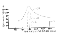
【0016】
図3に、本発明の局部発振回路のスプリアス妨害発生図を、図4に、従来の局部発振回路のスプリアス妨害発生図を示す。本発明の局部発振回路による逓倍出力は、270MHzが基本発振出力31となり、2次逓倍出力32は540MHzとなる。これが、本発明の局部発振回路特徴である。また、図示していないが、受信機の受信する回線周波数は、270MHzの近傍にある。妨害レベル33は出力31近傍に発生するが、これらはスーパーヘテロダイン受信機の場合、周波数変換後に中間周波数そのものに落ち込んでくる妨害は、急峻なRFフィルタで、また、回線周波数から数10KHz離れている妨害は、周波数変換後の中間周波数フィルタで減衰させることになる。
【0017】
近年は、直接変換方式が開発されており、これは、回線周波数を直接ベースバンド信号に変換するもので、中間周波数が無い。また局部発振信号は回線周波数とほぼ一致しているため、先に述べた中間周波数に落ち込む妨害はスーパーヘテロダイン方式に比べると大幅に減る。一部残る妨害は、局部発振回路からの不要逓倍出力に一致したものだけになる。この方式の場合、前述の不要逓倍出力が全く無ければ、スプリアス妨害はRFフィルタなしでも飛躍的に改善されるわけである。
【0018】
図3において、2次逓倍出力32があるがそのレベルは小さく、トランジスタ3の周波数特性が一般には周波数が高くなると利得が低下する領域で使用しているため、妨害を殆ど受けない。また、バンドパスフィルタ特性30を加味すればさらに耐妨害特性が向上する。バンドパスフィルタは図2でいう共振回路25、26をいう。
【0019】
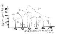
図4において、従来の水晶発振回路では、270MHzは、3次逓倍出力41となり、これが混合回路にて使用されるが、その他の不要逓倍出力42も混合回路に入る。バンドパスフィルタ特性30を図3と同じとすると、特に2、4次逓倍出力の減衰が不足し、スプリアス妨害レベル43が現われる。その耐妨害比は40dBしかない。スプリアス妨害特性は、アンテナからの外来妨害のレベルでも決まるので、従来は、アンテナの選択性やRFフィルタで、レベル43を減衰させていた。しかし、さらなる装置の小型化により、RFフィルタを挿入する余地が減り、またアンテナの選択性も大きくはないのが現状である。
【0020】
本発明を利用することにより、直接変換方式を使用した無線機には、RFフィルタ、あるいはインダクタなどの大型部品を省略でき、小型化をさらに進めることができる。これは腕装着型無線機にとって大きな利点を有するものである。
【0021】
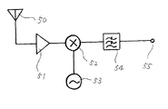
図5は、本発明の腕装着型無線機のRF回路部ブロック図である。アンテナ50で受信した信号を高周波増幅回路51で増幅し、混合回路52で局部発振回路53からの必要な逓倍出力信号と混合され、IF信号に変換する。中間周波フィルタ54は、受信周波数近傍のチャンネル選択度特性を向上させるためのものである。そして、端子55以降に、検波回路やデータデコーダ回路が続く。詳しくは、図7で説明する。
【0022】
従来は、スプリアス妨害特性を向上させるため、高周波増幅回路51の次にRFフィルタが挿入されていた。しかし、本発明の局部発振回路を使用すれば、RFフィルタを省略できる。特に、直接変換方式を使用した無線機は、スプリアス妨害の一つである、イメージ妨害が原理的に発生しないため、非常に有効である。
【0023】
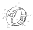
図6に、本発明の腕装着型無線機の外観図を示す。腕に取り付けるために尾錠金具61を用い、バンド長さを変えるための位置決め棒62が、穴部63に差し込まれている。余ったバンドは、バンド留め65で留められている。本体66には表示部67とボタンスイッチ68があり、受信情報や時刻情報を確認したり変更することができる。この形態は、普通の腕時計にも用いられている。バンド64a、bの内部には、アンテナが組み込まれており回線周波数を受信する。
【0024】
図7は本発明の腕装着型無線機の回路ブロック図である。本実施例の無線機は、先に説明したアンテナ101と、送受信無線部102と、波形整形回路103が備えられている。また、上記の無線部102と波形整形回路103への電源供給を制御する電源制御回路104と、この回路104を制御する制御部105が備えられている。本実施例の無線機はさらに、この制御部105にて比較される固有呼出番号が記載されているP−ROM(プログラマブル、リードオンリーメモリ)106と、固定呼出番号に付随する伝達情報が記載されるRAM(ランダムアクセスメモリ)109と、情報が表示されるLCD(液晶表示器)112を制御するLCD駆動回路110と、この駆動回路110の制御に使用されるクロック信号が発振される発振回路111とが設置されている。そして、電源制御回路104、制御部105、RAM109、LCD駆動回路110及び発振回路111により、メッセージ処理部114が構成されている。このメッセージ処理部114で処理されたメッセージを表示するLCD112と、メッセージの記憶されていることを伝達するための警報駆動回路107およびブザー、LED或はバイブレーターなどの警報装置108が設置されている。そして、この無線機を操作するための外部操作部113が設けられている。
【0025】
このような構成において、所定の回線周波数で送信されている信号は、アンテナ101を介し、無線部102で復調される。そして、波形整形回路103で矩形波に変換される。この無線部102と、波形整形回路103に対しては、電源制御回路104により制御部105の制御に基づき、信号を受信している時間に限り電源が供給される。
【0026】
制御部105は、上記の電源供給を管理するためのバッテリーセイビングタイミング信号を発生し、電源供給回路104を制御すると共に、受信信号とのビット同期、フレーム同期を行う。さらに、P−ROM106に記録されている固有呼出番号と、波形整形回路103から供給される矩形波化された受信信号との比較が誤り制御付きで行われ、記憶されている固有呼出番号が、呼び出されたか否かの判定が行われる。また、水晶などの基準信号源である発振回路111からの信号を計測する計測機能も有している。
【0027】
そして、呼出が確認されると、固有呼出番号に続きメッセージデータが受信され、RAM109に記憶される。そして、警報駆動回路107を介して、警報装置108により、使用者に呼出があったことを知らせる。RAM109に記憶されているメッセージは、スイッチ類から成る外部操作部113を操作することにより、制御部105を介してLCD駆動回路110に送られ、LCD112によって表示される。このLCD駆動回路110には発振回路111からのクロック信号が送られる。
【0028】
本発明の腕装着型無線機は、以上のような構成をとる。
【0029】
【発明の効果】
以上述べたように本発明の腕装着型無線機は、局部阪神回路部の共振素子として表面弾性波素子を使用し、直接変換方式を採用しているため、スーパーヘテロダイン受信機などと比較して、中間周波数に落ち込む妨害を大幅に減少させることができる。また、中間周波数に落ち込む妨害として、一部残る妨害は、局部発振回路からの不要逓倍出力に一致したものとなるが、帰還増幅手段を周波数が高くなると利得が低下する領域で使用するとともに、アンテナ素子の長さは、無線送受信回路部の容量成分と共働して、受信周波数の成分を選択的に通過させるのに十分な共振カーブ特性を有すべく設定されているので、スプリアス妨害の影響を低減することができる。
従って、耐妨害特性を向上させるために、RFフィルタやインダクタなどの大型部品を用いる必要が無いので、無線機本体を飛躍的に小型化することができるとともに、インダクタを用いる必要がないので異常発振が発生せず、SAW共振子による発振が最初からなされて、選択性が良く保たれる。
また、無線送受信回路部及び波形整形回路への電源供給を制御する電源制御回路と、信号受信している時間に限り前記無線送受信回路部及び前記波形整形回路へ電源制御回路に電源を供給させる制御部と、を備えているので、電力消費量を低減できる。
【図面の簡単な説明】
【図1】本発明の腕装着型無線機の局部発振回路部を示す回路図である。
【図2】従来の水晶振動子を用いた局部発振回路図である。
【図3】本発明の局部発振回路のスプリアス妨害発生図である。
【図4】従来の局部発振回路のスプリアス妨害発生図である。
【図5】本発明の腕装着型無線機のRF回路部ブロック図である。
【図6】本発明の腕装着型無線機の外観図を示す。
【図7】本発明の腕装着型無線機の回路ブロック図である。
【符号の説明】
1 表面弾性波素子
2 可変コンデンサ
3 トランジスタ
4、5、7 コンデンサ
6、8、9 抵抗
10 インダクタ
11 コンデンサ
12 結合コンデンサ
13、14 端子
15 グランド
16 混合回路
20 水晶振動子
21、22 インダクタ
23 コンデンサ
24 端子
25、26 共振回路
30 バンドパスフィルタ特性
31 基本発振出力
32 2次逓倍出力
33 妨害レベル
41 3次逓倍出力
42 不要逓倍出力
43 スプリアス妨害レベル
50 アンテナ
51 高周波増幅回路
52 混合回路
53 局部発振回路
54 中間周波フィルタ
55 端子
61 尾錠金具
62 位置決め棒
63 穴部
64a,b バンド
65 バンド留め
66 本体
67 表示部
68 ボタンスイッチ
101 アンテナ
102 送受信無線部
103 波形整形回路
104 電源制御回路
105 制御部
106 P−ROM
107 警報駆動回路
108 警報装置
109 RAM
110 駆動回路
111 発振回路
112 LCD
113 外部操作部
114 メッセージ処理部[0001]
[Industrial application fields]
The present invention relates to a local oscillating circuit of an arm-mounted radio.
[0002]
[Prior art]
Conventionally, as a resonant element used for a local oscillation circuit of a small portable radio, a VCO (voltage controlled oscillator) using a crystal resonator for a fixed frequency and a PLL (Phase Lock Loop) for a plurality of frequencies is used. It is used. Both have highly stable oscillation characteristics and are widely used.
[0003]
Even in the wrist-worn radio, a selective call receiver used at a fixed frequency has been commercialized. A resonant element used in these local oscillation circuits is a crystal resonator.
[0004]
A surface acoustic wave element (SAW device) is widely used as an element for attenuating unnecessary signals in a narrow band, such as an RF filter.
[0005]
[Problems to be solved by the invention]
The oscillation frequency of the local oscillation circuit using a crystal resonator is generally 3rd to 5th order overtone vibration due to the relationship between the fundamental vibration mode of the crystal and low power consumption, and this frequency becomes the fundamental frequency. Multiply by the circuit to obtain the desired output signal.
[0006]
For this reason, an unnecessary oscillation signal is generated in the multiplier circuit section. Unwanted oscillation appears as spurious interference (unnecessary signal interference) to the receiver, which may deteriorate the characteristics of the radio.
[0007]
Conventionally, these unnecessary oscillations have been suppressed by narrow-band bandpass filters, but large parts such as filters can no longer be introduced due to space limitations due to the miniaturization of radios, and spurious characteristics are sacrificed. There was a problem that has been made.
[0008]
On the other hand, the SAW device may be used as a resonator by utilizing the narrow band property.
[0009]
[Means for Solving the Problems]
In order to solve the above problems, an arm-mounted radio device according to the present invention includes an antenna element having a predetermined selectivity and a radio transmission / reception circuit unit. The wireless transmission / reception circuit unit includes a local oscillation circuit and a frequency conversion circuit, and the frequency conversion circuit frequency-converts a transmission / reception signal by a direct conversion method using an output signal of the local oscillation circuit, and the local oscillation circuit The circuit is used in a local oscillation element composed of a surface acoustic wave element, and in a region where the gain decreases as the frequency increases, and the oscillation signal of the local oscillation element is feedback-amplified to obtain a frequency substantially equal to the frequency of the transmission / reception signal. Feedback amplifier means for outputting as the output signal, and a coupling capacitor for transmitting the output signal to the frequency conversion circuit via a terminal portion, and the length of the antenna element is that of the wireless transmission / reception circuit portion It is set to have a resonance curve characteristic sufficient to selectively pass the received frequency component in cooperation with the capacitive component,
A power supply control circuit for controlling power supply to the wireless transmission / reception circuit unit and the waveform shaping circuit;
And a control unit that supplies power to the power control circuit to the radio transmission / reception circuit unit and the waveform shaping circuit only during a time during which a signal is received.
[0012]
The present invention provides a circuit configuration that dramatically improves spurious interference characteristics even in an ultra-small radio such as an arm-mounted radio.
[0013]
【Example】
Hereinafter, details of the present invention will be described by way of examples.
[0014]
FIG. 1 is a circuit diagram showing a local oscillation circuit unit of an arm-mounted radio device according to the present invention. A surface acoustic wave element (SAW resonator) 1 is a characteristic part of the present invention. The SAW resonator is characterized in that the reactance is inductive and close to zero at several hundred MHz compared to a conventional crystal resonator, and the loss in the vicinity is very small. Furthermore, it has a high Q and can be used as a local oscillation element.
[0015]
In FIG. 1, a variable capacitor 2 is an element for adjusting the oscillation frequency. Although this circuit is a Colpitts type oscillation circuit, the
[0016]
FIG. 3 shows a spurious interference generation diagram of the local oscillation circuit of the present invention, and FIG. 4 shows a spurious interference generation diagram of the conventional local oscillation circuit. As for the multiplication output by the local oscillation circuit of the present invention, 270 MHz becomes the
[0017]
In recent years, a direct conversion method has been developed, which directly converts a line frequency into a baseband signal and has no intermediate frequency. In addition, since the local oscillation signal substantially matches the line frequency, the above-described disturbance falling to the intermediate frequency is greatly reduced compared to the superheterodyne system. The only remaining interference is the one that matches the unwanted multiplied output from the local oscillator circuit. In the case of this method, if there is no unnecessary multiplication output as described above, spurious interference can be drastically improved without an RF filter.
[0018]
In FIG. 3, there is a secondary multiplied
[0019]
In FIG. 4, in the conventional crystal oscillation circuit, 270 MHz becomes the third-order multiplied
[0020]
By utilizing the present invention, large parts such as an RF filter or an inductor can be omitted from a radio device using the direct conversion method, and further miniaturization can be promoted. This has a great advantage for an arm-mounted radio.
[0021]
FIG. 5 is a block diagram of the RF circuit unit of the wrist-worn radio according to the present invention. The signal received by the
[0022]
Conventionally, an RF filter has been inserted after the high-
[0023]
FIG. 6 shows an external view of the wrist-worn radio of the present invention. A buckle fitting 61 is used to attach to the arm, and a positioning rod 62 for changing the band length is inserted into the hole 63. The surplus band is fastened with a band clamp 65. The main body 66 includes a display unit 67 and a
[0024]
FIG. 7 is a circuit block diagram of the wrist-worn radio of the present invention. The wireless device of this embodiment includes the
[0025]
In such a configuration, a signal transmitted at a predetermined line frequency is demodulated by the
[0026]
The
[0027]
When the call is confirmed, message data is received following the unique call number and stored in the
[0028]
The arm-mounted radio device of the present invention has the above configuration.
[0029]
【The invention's effect】
As described above, the wrist-worn radio of the present invention uses a surface acoustic wave element as a resonance element of the local Hanshin circuit section and adopts a direct conversion method, so compared with a superheterodyne receiver or the like. The interference that falls to the intermediate frequency can be greatly reduced. In addition, as interference that falls to the intermediate frequency, part of the interference that remains is the same as the unnecessary multiplied output from the local oscillation circuit, but the feedback amplification means is used in a region where the gain decreases as the frequency increases, and the antenna The element length is set to have a resonance curve characteristic sufficient to selectively pass the reception frequency component in cooperation with the capacitance component of the radio transmission / reception circuit unit. Can be reduced.
Therefore, since it is not necessary to use large parts such as an RF filter and an inductor in order to improve the anti-jamming characteristics, it is possible to drastically reduce the size of the radio main body and abnormal oscillation because there is no need to use an inductor. Oscillation does not occur, and oscillation by the SAW resonator is performed from the beginning, and the selectivity is maintained well.
Also, a power control circuit that controls power supply to the wireless transmission / reception circuit unit and the waveform shaping circuit, and a control for supplying power to the power transmission control circuit to the wireless transmission / reception circuit unit and the waveform shaping circuit only during the time of signal reception. Power consumption can be reduced.
[Brief description of the drawings]
FIG. 1 is a circuit diagram showing a local oscillation circuit unit of a wrist-worn radio according to the present invention.
FIG. 2 is a local oscillation circuit diagram using a conventional crystal resonator.
FIG. 3 is a spurious interference generation diagram of the local oscillation circuit of the present invention.
FIG. 4 is a spurious interference generation diagram of a conventional local oscillation circuit.
FIG. 5 is a block diagram of the RF circuit unit of the wrist-worn radio according to the present invention.
FIG. 6 is an external view of an arm-mounted radio device according to the present invention.
FIG. 7 is a circuit block diagram of the wrist-worn radio of the present invention.
[Explanation of symbols]
DESCRIPTION OF SYMBOLS 1 Surface acoustic wave element 2 Variable capacitor 3
107
110
113
Claims (1)
前記無線送受信回路部は、局部発振回路と周波数変換回路とを備え、
前記周波数変換回路は、前記局部発振回路の出力信号を用いて送受信信号を直接変換方式により周波数変換させており、
前記局部発振回路は、表面弾性波素子からなる局部発振素子と、周波数が高くなると利得が低下する領域で使用され、該局部発振素子の発振信号を帰還増幅して前記送受信信号の周波数とほぼ一致する周波数を有する前記出力信号として出力する帰還増幅手段と、前記出力信号を前記周波数変換回路に伝達する結合コンデンサと、を有し、
前記アンテナ素子の長さは、前記無線送受信回路部の容量成分と共働して、受信周波数の成分を選択的に通過させるのに十分な共振カーブ特性を有すべく設定されており、
前記無線送受信回路部及び前記波形整形回路への電源供給を制御する電源制御回路と、
前記電源制御回路により、信号受信している時間に限り前記無線送受信回路部及び前記波形整形回路へ電源を供給させる制御部と、を備えた、
ことを特徴とする腕装着型無線機器。In an arm-mounted radio including an antenna element having a predetermined selectivity, a radio transmission / reception circuit unit, and a waveform shaping circuit,
The wireless transmission / reception circuit unit includes a local oscillation circuit and a frequency conversion circuit,
The frequency conversion circuit frequency-converts a transmission / reception signal by a direct conversion method using an output signal of the local oscillation circuit,
The local oscillation circuit is used in a region where a gain decreases as the frequency increases, and a local oscillation element made of a surface acoustic wave element. Feedback amplification means for outputting as the output signal having a frequency to be coupled, and a coupling capacitor for transmitting the output signal to the frequency conversion circuit,
The length of the antenna element is set to have a resonance curve characteristic sufficient to selectively pass the component of the reception frequency in cooperation with the capacitance component of the wireless transmission / reception circuit unit,
A power supply control circuit for controlling power supply to the wireless transmission / reception circuit unit and the waveform shaping circuit;
The power supply control circuit includes a control unit that supplies power to the wireless transmission / reception circuit unit and the waveform shaping circuit only during the time of signal reception.
An arm-mounted wireless device characterized by that.
Priority Applications (1)
| Application Number | Priority Date | Filing Date | Title |
|---|---|---|---|
| JP14521593A JP3610080B2 (en) | 1993-06-16 | 1993-06-16 | Arm-mounted radio |
Applications Claiming Priority (1)
| Application Number | Priority Date | Filing Date | Title |
|---|---|---|---|
| JP14521593A JP3610080B2 (en) | 1993-06-16 | 1993-06-16 | Arm-mounted radio |
Publications (2)
| Publication Number | Publication Date |
|---|---|
| JPH077455A JPH077455A (en) | 1995-01-10 |
| JP3610080B2 true JP3610080B2 (en) | 2005-01-12 |
Family
ID=15380038
Family Applications (1)
| Application Number | Title | Priority Date | Filing Date |
|---|---|---|---|
| JP14521593A Expired - Fee Related JP3610080B2 (en) | 1993-06-16 | 1993-06-16 | Arm-mounted radio |
Country Status (1)
| Country | Link |
|---|---|
| JP (1) | JP3610080B2 (en) |
-
1993
- 1993-06-16 JP JP14521593A patent/JP3610080B2/en not_active Expired - Fee Related
Also Published As
| Publication number | Publication date |
|---|---|
| JPH077455A (en) | 1995-01-10 |
Similar Documents
| Publication | Publication Date | Title |
|---|---|---|
| JPS63290414A (en) | Automobile telephone set | |
| JP2001237640A (en) | Voltage controlled oscillator and communication equipment | |
| JP2516850B2 (en) | Mechanical resonant oscillator circuit | |
| JP3610080B2 (en) | Arm-mounted radio | |
| JPH04134913A (en) | Crystal oscillator | |
| JP3893932B2 (en) | Voltage controlled oscillator | |
| JPWO2006106860A1 (en) | Television tuner | |
| JPS63131728A (en) | Double superheterodyne system radio equipment | |
| KR970011588B1 (en) | Voltage controlled oscillator | |
| JPH0799475A (en) | Data communication equipment | |
| WO2006127817A2 (en) | Oscillator coupling to reduce spurious signals in receiver circuits | |
| JPS6014526A (en) | All-band double heterodyne am receiver | |
| JPH0685697A (en) | Radio transmitter | |
| JPH0669155B2 (en) | Small transceiver | |
| KR100499746B1 (en) | Radio Frequency communication module | |
| JPS60214123A (en) | Antenna common use device | |
| JP2002043843A (en) | Voltage-controlled oscillator and communication apparatus using the same | |
| KR950004839Y1 (en) | Wireless calling receiver | |
| JPS6148239A (en) | Am receiver | |
| JPH03204205A (en) | Integrated circuit device | |
| KR0125414Y1 (en) | Codeless telephone down converter | |
| Ash | Optimal application of SAW devices in spread spectrum and other RF systems | |
| JP2001284964A (en) | Oscillator | |
| JPS61234128A (en) | Amplitude modulation receiver | |
| JPH0654326U (en) | Transmitter |
Legal Events
| Date | Code | Title | Description |
|---|---|---|---|
| A521 | Written amendment |
Free format text: JAPANESE INTERMEDIATE CODE: A523 Effective date: 20040722 |
|
| A61 | First payment of annual fees (during grant procedure) |
Free format text: JAPANESE INTERMEDIATE CODE: A61 Effective date: 20041018 |
|
| R150 | Certificate of patent or registration of utility model |
Free format text: JAPANESE INTERMEDIATE CODE: R150 |
|
| FPAY | Renewal fee payment (event date is renewal date of database) |
Free format text: PAYMENT UNTIL: 20081022 Year of fee payment: 4 |
|
| FPAY | Renewal fee payment (event date is renewal date of database) |
Free format text: PAYMENT UNTIL: 20091022 Year of fee payment: 5 |
|
| FPAY | Renewal fee payment (event date is renewal date of database) |
Free format text: PAYMENT UNTIL: 20101022 Year of fee payment: 6 |
|
| FPAY | Renewal fee payment (event date is renewal date of database) |
Free format text: PAYMENT UNTIL: 20101022 Year of fee payment: 6 |
|
| FPAY | Renewal fee payment (event date is renewal date of database) |
Free format text: PAYMENT UNTIL: 20111022 Year of fee payment: 7 |
|
| FPAY | Renewal fee payment (event date is renewal date of database) |
Free format text: PAYMENT UNTIL: 20121022 Year of fee payment: 8 |
|
| LAPS | Cancellation because of no payment of annual fees |