JP3608874B2 - Ultrasonic probe - Google Patents
Ultrasonic probe Download PDFInfo
- Publication number
- JP3608874B2 JP3608874B2 JP14468096A JP14468096A JP3608874B2 JP 3608874 B2 JP3608874 B2 JP 3608874B2 JP 14468096 A JP14468096 A JP 14468096A JP 14468096 A JP14468096 A JP 14468096A JP 3608874 B2 JP3608874 B2 JP 3608874B2
- Authority
- JP
- Japan
- Prior art keywords
- ultrasonic
- ultrasonic transducer
- layer
- piezoelectric
- piezoelectric element
- Prior art date
- Legal status (The legal status is an assumption and is not a legal conclusion. Google has not performed a legal analysis and makes no representation as to the accuracy of the status listed.)
- Expired - Lifetime
Links
Images


Landscapes
- Ultra Sonic Daignosis Equipment (AREA)
- Transducers For Ultrasonic Waves (AREA)
- Investigating Or Analyzing Materials By The Use Of Ultrasonic Waves (AREA)
Description
【0001】
【発明の属する技術分野】
本発明は、超音波診断装置等において超音波を打ち出すと共にその反射波を受信する超音波探触子に関し、特に所定の厚さの板状に形成された圧電素子を複数層積層して成る超音波振動子の反りの発生を少なくして仕上がりの寸法サイズを高精度とすることができる超音波探触子に関する。
【0002】
【従来の技術】
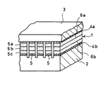
従来のこの種の超音波探触子は、図7に示すように、超音波を打ち出すと共にその反射波を受信する超音波振動子1と、この超音波振動子1の背面に設けられその背面から出る超音波が再び振動子面に戻ってこないようにするバッキング材2と、上記超音波振動子1の前面に設けられ該超音波振動子1の音響インピーダンスと生体の音響インピーダンスとの整合をとる音響整合層3とを有して成っていた。なお、上記超音波振動子1の上面及び下面には、それぞれ外部電極4a,4bが設けられており、両電極4a,4b間に電圧を印加することにより、圧電材料から成る超音波振動子1をその厚さ方向に伸縮させるようになっている。また、図7においては、超音波振動子1は所定のピッチ幅で短冊形に切断されており、この短冊形の多数の振動子素子5,5,…をアレイ状に配列したものを示している。
【0003】
上記多数の振動子素子5,5,…をアレイ状に配列した超音波振動子1を例えば電子セクタ走査用探触子に用いる場合、各振動子素子5,5,…のピッチ幅は、得られる超音波画像のアーチファクトの原因となるグレイティングローブの発生を避けるためにできるだけ小さくする必要がある。しかし、上記各振動子素子5,5,…のピッチ幅を小さくすると、1素子当たりの圧電材料のサイズは小さくなり、その結果電気的容量が小さくなる一方、電気的インピーダンスは大きくなる。また、多数の振動子素子5,5,…を二次元方向にアレイ状に配列した超音波振動子1を用いた二次元アレイ探触子の場合は、1素子当たりの圧電材料のサイズはさらに小さくなる。このような、電気的容量の低下及び電気的インピーダンスの増大は、超音波診断装置本体側の送波回路系との電気的整合が悪く、また超音波診断装置本体と接続するケーブルの容量の影響を受けて電気的整合が悪く、超音波探触子としてのS/Nを劣化させるものであった。
【0004】
これに対し、上記超音波振動子1の1素子当たりの電気的容量の低下及び電気的インピーダンスの増大を抑える方策として、図8に示すように、超音波振動子1を構成する圧電材料を薄く形成し、これを複数層たとえば3層積層し(5a,5b,5c)、各層の間に内部電極6a,6bを挿入した構造のものがある。この場合、3層の積層構造では、上面の外部電極4aを2層目の内部電極6bに接続し、下面の外部電極4bを1層目の内部電極6aに接続して、積層方向に交互に逆向きに分極した構造とされている。このようにすると、3層に積層された圧電素子5a,5b,5cが音響的には直列となり、電気的には並列接続となる。この結果、図7に示す単層の超音波振動子1と図8に示す3層の超音波振動子1とが同じ厚さの場合には、両者の共振周波数は等しくなるが、一般にn層積層の圧電材料では1層当たりの厚さが1/nで面積がn倍になるため、電気的容量はn2倍、電気的インピーダンスは1/n2となる。
【0005】
そして、このような複数層積層構造の超音波振動子1の製造方法としては、複数層積層した圧電素子5a,5b,5cと各層間に挿入された内部電極6a,6bとを同時に焼成することにより一体化する一体焼成積層法が用いられていた。
【0006】
【発明が解決しようとする課題】
しかし、このような従来の複数層積層構造の超音波振動子1においては、複数層積層した圧電素子5a,5b,5cと各層間に挿入された内部電極6a,6bとを同時に焼成することにより、焼成後に超音波振動子1の反りが発生すると共に、その反りの程度がばらつき、且つ厚みのばらつきが発生し、高精度の寸法サイズの超音波振動子1を製造するのが難しかった。特に、1層当たりの圧電材料の厚さが増すほど上記の問題点が顕著となるものであった。このことから、従来の超音波探触子としては、単一共振周波数の振動モードが得られないことがあり、超音波診断装置として画質のよい超音波画像が得られないことがあった。
【0007】
そこで、本発明は、このような問題点に対処し、所定の厚さの板状に形成された圧電素子を複数層積層して成る超音波振動子の反りの発生を少なくして仕上がりの寸法サイズを高精度とすることができる超音波探触子を提供することを目的とする。
【0008】
【課題を解決するための手段】
上記目的を達成するために、本発明による超音波探触子は、超音波を打ち出すと共にその反射波を受信する超音波振動子と、この超音波振動子の背面に設けられその背面からの超音波の戻りを防止するバッキング材と、上記超音波振動子の前面に設けられ該超音波振動子の音響インピーダンスと生体の音響インピーダンスとの整合をとる音響整合層とを有して成る超音波探触子において、上記超音波振動子は、所定の厚さの板状に形成された圧電素子を複数層積層し、この積層された圧電素子の全体の上面及び下面に外部電極を形成し、上記圧電素子の各層の境目には平板状の内部電極をそれぞれ形成し、かつ上記圧電素子の各層の厚み内には一又は複数の平板状の変形防止材を挿入した構造としたものである。
【0009】
また、上記圧電素子の各層の厚み内に挿入された平板状の変形防止材は、平板状の内部電極と熱膨張率が同一又は同等の材料から成るものとする。
【0010】
さらに、上記圧電素子の各層の厚み内に挿入された平板状の変形防止材は、導電材料又は絶縁材料から成るものとする。
【0013】
【発明の実施の形態】
以下、本発明の実施の形態を添付図面に基づいて詳細に説明する。
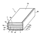
図1は本発明による超音波探触子の実施の形態を示す一部断面斜視図である。この超音波探触子は、超音波診断装置等において超音波を打ち出すと共にその反射波を受信するもので、図1に示すように、超音波振動子1と、バッキング材2と、音響整合層3とから成る。
【0014】
上記超音波振動子1は、超音波を打ち出すと共にその反射波を受信するもので、電気エネルギーと超音波エネルギーとを変換する圧電材料で構成されている。この圧電材料としては、例えばジルコン・チタン酸鉛(PZT)系の圧電セラミックス又はチタン酸鉛(PbTiO3)系の圧電セラミックスなどがある。PZT系の圧電セラミックスは、電気エネルギーと超音波エネルギーとの変換効率を表わす電気機械結合係数が大きいことと、誘電率が大きく電気回路系との電気的インピーダンス整合がとりやすいという特徴がある。また、PbTiO3系の圧電セラミックスは、横効果の振動結合が著しく弱いことから、不要振動が激減し、純粋に厚み縦振動のみの理想に近い送受波特性が得られる点に特徴がある。
【0015】
バッキング材2は、上記超音波振動子1の背面に設けられその背面から出る超音波が再び振動子面に戻ってこないようにするもので、超音波の減衰の大きい材料を使用している。また、音響整合層3は、上記超音波振動子1の前面に設けられ該超音波振動子1の音響インピーダンスと生体の音響インピーダンスとの整合をとるもので、これにより超音波振動子1の振動が効率よく生体に伝播できるようになる。なお、この音響整合層3は、2層設けてもよい。また、図1では省略しているが、上記音響整合層3のさらに前面に音響レンズを設けてもよい。
【0016】
なお、上記超音波振動子1の上面及び下面には、それぞれ外部電極4a,4bが設けられており、両電極4a,4b間に電圧を印加することにより、圧電材料から成る超音波振動子1をその厚さ方向に伸縮させて超音波を発生させるようになっている。また、図1においては、超音波振動子1は所定のピッチ幅で短冊形に切断されており、この短冊形の多数の振動子素子5,5,…をアレイ状に配列したものを示している。
【0017】
ここで、本発明においては、上記超音波振動子1は、図2に示すように、所定の厚さの板状に形成された圧電素子5a,5b,5cを複数層積層し、この複数層積層された圧電素子5a〜5cの全体の上面及び下面に外部電極4a,4bを形成すると共に、各層の境目には平板状の内部電極6a,6bをそれぞれ形成し、かつ上記圧電素子5a,5b,5cの各層の厚み内には一又は複数の平板状の変形防止材7,7,…が等間隔で挿入されている。
【0018】
すなわち、例えば1層の厚さが0.21mm程度の圧電素子5a,5b,5cを3層積層し、各層5a,5b,5cの境目には平板状の内部電極6a,6bをそれぞれ形成し、かつ各圧電素子5a,5b,5cの厚み内には例えば0.07mm間隔で2枚の平板状の変形防止材7,7,…が挿入されている。従って、図2の例による超音波振動子1は、例えば0.07mmの厚さの圧電素子を9枚積層して、全体で約0.63mmの厚さになる。そして、上記変形防止材7,7,…は、内部電極6a,6bと同一の材料でできており、その内部電極6a,6bと熱膨張率が同一の導電材料から成る。
【0019】
このような状態で、上記上面の外部電極4a及び下面の外部電極4bをそれぞれ1層おきに異なる内部電極6a,6bに対し接続すると共に、各層内の平板状の変形防止材7,7,…とは絶縁する。すなわち、上面の外部電極4aと連続する一方の側部電極8aを設け、この側部電極8aの一部を2層目の内部電極6bに接続し、下面の外部電極4bと連続する他方の側部電極8bを設け、この側部電極8bの一部を1層目の内部電極6aに接続する。このとき、一方の側部電極8aは、2層目の内部電極6bに接続する部分以外は絶縁物が充填されるなどして他の内部電極6a及び変形防止材7,7,…とは絶縁されている。また、他方の側部電極8bは、1層目の内部電極6aに接続する部分以外は絶縁物が充填されるなどして他の内部電極6b及び変形防止材7,7,…とは絶縁されている。これにより、上面の外部電極4aは2層目の内部電極6bにのみ接続され、下面の外部電極4bは1層目の内部電極6aにのみ接続される。この結果、3層に積層された圧電素子5a,5b,5cが音響的には直列となり、電気的には並列接続となる。
【0020】
そして、この状態で上記複数層積層された圧電素子5a〜5cの全体を積層方向に交互に逆向きに分極した構造とする。すなわち、上面の外部電極4aと下面の外部電極4bとの間に直流高電界を印加して分極処理を行い、圧電素子5a〜5cの各層を分極し、圧電性を付与する。これにより、本発明に係る超音波振動子1が構成される。この場合、各層の圧電素子5a,5b,5c内に挿入された変形防止材7,7,…の存在により、複数層積層された圧電素子5a〜5cの全体を焼成する際の反りの発生を少なくし、仕上がりの寸法サイズを高精度とすることができる。なお、図2においては、音響整合層3を2層(3a,3b)設けた場合を示している。また、上記変形防止材7を、内部電極6a,6bと熱膨張率が同一の材料から成るものとしたことにより、複数層積層された圧電素子5a,5b,5cの全体を焼成する際の反りの発生をさらに少なくし、仕上がりの寸法サイズをさらに高精度とすることができる。
【0021】
なお、図1及び図2においては、超音波振動子1は、圧電素子を3層(5a,5b,5c)積層したものとしたが、本発明はこれに限らず、2層以上の複数層であれば何層でもよい。また、各層の圧電素子5a,5b,5c内に挿入する変形防止材7,7,…も2枚に限らず、何枚であってもよい。さらに、上記変形防止材7は、内部電極6a,6bと熱膨張率が同一の材料から成るものとしたが、これに限らず、略同等の熱膨張率の材料から成るものであってもよい。さらにまた、上記変形防止材7は、内部電極6a,6bと熱膨張率が同一又は同等の材料から成るものであるならば、導電材料又は絶縁材料のどちらであってもよい。変形防止材7が絶縁材料であるならば、上述の説明において、側部電極8a,8bの内側面と上記変形防止材7の端部との間に絶縁物を充填する必要はない。
【0022】
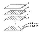
次に、上記超音波探触子の製造方法について、図3及び図4を参照して説明する。まず、図3において、圧電材料を用いて所定の厚さで平板状の圧電素子片9,9,…を形成する。すなわち、圧電材料としてPZT系又はPbTiO3系の圧電セラミックス粉末を用い、これに有機バインダを加え、ドクターブレード法と呼ばれる製法により所定の厚さで平板状の圧電素子片9を作製する。このとき、その厚さは以後の圧着焼成工程での収縮を考慮し、焼成後に研磨しなくても所定の厚さ、例えば厚さ0.07mmとなるように設定すればよい。
【0023】
次に、上記圧電素子片9の片面に図2に示す内部電極6a,6bとなる導電ペースト10を印刷塗布し、この導電ペースト10を印刷塗布した複数枚の圧電素子片9,9,…を積層して加熱圧着する。すなわち、導電ペースト10として銀パラジウム等の材料を用い、この銀パラジウム等をスクリーン印刷等により、圧電素子片9の表面全体に塗布する。このとき、一番上に位置する圧電素子片9の表面には上記の導電ペースト10を印刷塗布しない。そして、上記導電ペースト10を印刷塗布した圧電素子片9,9,…を乾燥した後、例えば9枚の圧電素子片9を積層し、金型中で加熱圧着する。
【0024】
次に、この加熱圧着された圧電素子片9,9,…の積層体を所定温度で焼成する。このとき、徐々に昇温しながら圧電素子片9中の有機バインダを除去し、さらに例えば1150℃で5時間焼成する。そして、この焼成後に、圧電素子片9,9,…の積層体の外形を所望の寸法に加工する。
【0025】
次に、上記複数層積層された圧電素子片9,9,…の全体の上面及び下面に外部電極4a,4b用の導電ペーストを焼き付け、上記上面の外部電極4a及び下面の外部電極4bをそれぞれ同数の複数層おきに異なる内部電極6a,6b用の導電ペーストに対し接続すると共に、その他の導電ペーストとは絶縁する。なお、上記外部電極4a,4bは導電材料を蒸着又はメッキ等により形成してもよい。そして、この実施例では図4に示すように、図3において9枚の圧電素子片9を積層したもののうち、下から数えて3枚目と6枚目の圧電素子片9の片面に塗布された導電ペーストはそれぞれ内部電極6b,6aとし、それ以外の圧電素子片9の片面に塗布された導電ペーストは総て変形防止材7としている。
【0026】
そして、上面の外部電極4aと連続する一方の側部電極8aを焼付け等により設け、この側部電極8aの一部を一方の内部電極6bに接続し、また下面の外部電極4bと連続する他方の側部電極8bを焼付け等により設け、この側部電極8bの一部を他方の内部電極6aに接続する。このとき、一方の側部電極8aは、上記内部電極6bに接続する部分以外は絶縁物が充填されるなどして他の内部電極6a及び変形防止材7,7,…とは絶縁されている。また、他方の側部電極8bは、上記内部電極6aに接続する部分以外は絶縁物が充填されるなどして他の内部電極6b及び変形防止材7,7,…とは絶縁されている。これにより、上面の外部電極4aは一方の内部電極6bにのみ接続され、下面の外部電極4bは他方の内部電極6aにのみ接続される。この結果、上記内部電極6a,6bを境にして3層に積層された圧電素子5a,5b,5cが音響的には直列となり、電気的には並列接続となる。
【0027】
その後、上記上面の外部電極4aと下面の外部電極4bとの間に直流高電界を印加して上記複数層積層された圧電素子片9,9,…の全体を分極処理して圧電性を付与し、超音波振動子1を構成する。この場合、各層の圧電素子5a,5b,5c内に挿入された変形防止材7,7,…の存在により、複数層積層された圧電素子5a〜5cの全体を焼成する際に反りの発生を少なくし、仕上がりの寸法サイズを高精度とすることができる。このように作製された超音波振動子1は、例えば上記内部電極6a,6bを境にして3層に積層された圧電素子5a,5b,5cの厚さがそれぞれ0.21mmとなり、全体の厚さが0.63mmとなる3層の積層構造の超音波振動子と等価となる。
【0028】
その後、図2に示すように、上記超音波振動子1の背面側にその背面から出る超音波が再び振動子面に戻ってこないようにするバッキング材2を設けると共に、上記超音波振動子1の前面側には該超音波振動子1の音響インピーダンスと生体の音響インピーダンスとの整合をとる音響整合層3a,3bを設ける。これにより、本発明の超音波探触子が製造される。
【0029】
なお、上記超音波探触子の製造工程において、図4に示すように超音波振動子1が作製されたところで、該超音波振動子1を所定のピッチ幅p,p,…で短冊形に切断してアレイ状に形成してもよい。この場合は、多数の振動子素子をアレイ状に配列した電子走査型の超音波探触子を製造することができる。
【0030】
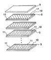
図5及び図6は超音波探触子の製造方法の他の例を示す説明図である。この例による製造方法は、基本的には図3及び図4に示す製造方法と同一であるが、圧電材料を用いて所定の厚さで平板状の圧電素子片9,9,…を形成した後、上記圧電素子片9の片面に図2に示す内部電極6a,6bとなる導電ペースト10を印刷塗布する際に、その両側辺部に導電ペースト10の塗布されていない絶縁部分11を形成したものである。なお、このとき、実際に図2に示す内部電極6a,6bとなる導電ペースト10を印刷塗布する際は、外部電極8a,8bと接続する側には絶縁部分11を形成しないようにする。
【0031】
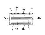
このような状態で、図6に示すように、9層の圧電素子片を積層すると共に内部電極6a,6b及び変形防止材7,7,…を形成し、かつ上面及び下面に外部電極4a,4bを形成し、さらに両側面に側部電極8a,8bを形成する。そして、上面の外部電極4aと連続する側部電極8aを一方の内部電極6bに接続し、下面の外部電極4bと連続する側部電極8bを他方の内部電極6aに接続する。このように製造することにより、図4において側部電極8a,8bの内側面と9層の圧電素子片の側端部との間に絶縁物を充填することを要せず、製造工程を簡略化できる。
【0032】
【発明の効果】
本発明による超音波探触子は以上のように構成されたので、その超音波振動子を、所定の厚さの板状に形成された圧電素子を複数層積層し、この積層された圧電素子の全体の上面及び下面に外部電極を形成し、上記圧電素子の各層の境目には平板状の内部電極をそれぞれ形成し、かつ上記圧電素子の各層の厚み内には一又は複数の平板状の変形防止材を挿入した構造としたことにより、上記変形防止材の挿入によって複数層積層された1層当たりの厚さを実質的に薄くできると共にその変形防止材の存在により、上記複数層積層された圧電素子の全体を焼成する際の反りの発生を少なくし、仕上がりの寸法サイズを高精度とすることができる。従って、本発明による超音波探触子によれば、単一共振周波数の振動モードが得られ、超音波診断装置として画質のよい超音波画像を得ることができる。
【図面の簡単な説明】
【図1】本発明による超音波探触子の実施の形態を示す一部断面斜視図である。
【図2】図1のA−A線断面図である。
【図3】上記超音波探触子の製造方法の工程の一部を示す斜視説明図である。
【図4】上記超音波探触子の製造方法で作製した超音波振動子を示す斜視説明図である。
【図5】他の例による超音波探触子の製造方法の工程の一部を示す斜視説明図である。
【図6】上記超音波探触子の製造方法で作製した超音波振動子を示す断面説明図である。
【図7】従来の超音波探触子を示す一部断面斜視図である。
【図8】従来の複数層積層構造の超音波振動子を有する超音波探触子を示す一部断面斜視図である。
【符号の説明】
1…超音波振動子
2…バッキング材
3,3a,3b…音響整合層
4a,4b…外部電極
5…振動子素子
5a,5b,5c…圧電素子
6a,6b…内部電極
7…変形防止材
8a,8b…側部電極
9…圧電素子片
10…導電ペースト
11…絶縁部分[0001]
BACKGROUND OF THE INVENTION
The present invention relates to an ultrasonic probe that emits ultrasonic waves and receives reflected waves in an ultrasonic diagnostic apparatus or the like, and more particularly, an ultrasonic probe formed by laminating a plurality of piezoelectric elements formed in a plate shape with a predetermined thickness. with less warping of wave oscillator relates dimension size of the finished ultrasonic feeler element, which may be a high precision.
[0002]
[Prior art]
As shown in FIG. 7, a conventional ultrasonic probe of this type includes an
[0003]
When the
[0004]
On the other hand, as a measure for suppressing a decrease in electrical capacity per element of the
[0005]
And as a manufacturing method of the ultrasonic transducer |
[0006]
[Problems to be solved by the invention]
However, in such a conventional
[0007]
Accordingly, the present invention addresses such problems and reduces the occurrence of warpage of an ultrasonic transducer formed by laminating a plurality of piezoelectric elements formed in a plate shape with a predetermined thickness to achieve a finished size. and an object thereof is to provide an ultrasonic feeler element which can be the size and precision.
[0008]
[Means for Solving the Problems]
To achieve the above object, the ultrasonic probe according to the present invention, an ultrasonic transducer for receiving the reflected wave with hammer out ultrasonic waves, from the back is provided on a back surface of the ultrasonic transducer ultrasonic An ultrasonic probe comprising a backing material for preventing the return of acoustic waves, and an acoustic matching layer provided on the front surface of the ultrasonic transducer for matching the acoustic impedance of the ultrasonic transducer with that of a living body. in probe, the ultrasonic transducer, the piezoelectric elements formed in a predetermined thickness of the plate-like multiple layers laminated, the external electrodes are formed on the upper surface and the lower surface of the whole product layer have been piezoelectric elements this , the boundary of each layer of the piezoelectric element plate-shaped inner electrodes are respectively formed, and is within the thickness of each layer of the piezoelectric element obtained by a structure in which insert one or more plate-like deformation preventing member is there.
[0009]
The flat plate-shaped deformation preventing material inserted within the thickness of each layer of the piezoelectric element is made of a material having the same or equivalent thermal expansion coefficient as the flat plate-like internal electrode.
[0010]
Furthermore, the flat plate-shaped deformation preventing material inserted within the thickness of each layer of the piezoelectric element is made of a conductive material or an insulating material.
[0013]
DETAILED DESCRIPTION OF THE INVENTION
Hereinafter, embodiments of the present invention will be described in detail with reference to the accompanying drawings.
FIG. 1 is a partial cross-sectional perspective view showing an embodiment of an ultrasonic probe according to the present invention. The ultrasonic probe emits ultrasonic waves and receives reflected waves in an ultrasonic diagnostic apparatus or the like. As shown in FIG. 1, the
[0014]
The
[0015]
The
[0016]
[0017]
Here, in the present invention, as shown in FIG. 2, the
[0018]
That is, for example, three layers of
[0019]
In this state, the
[0020]
In this state, the whole of the
[0021]
In FIGS. 1 and 2, the
[0022]
Next, manufacturing method of the ultrasonic probe will be described with reference to FIGS. First, in FIG. 3, flat
[0023]
Next, a
[0024]
Next, the laminated body of the
[0025]
Next, a conductive paste for the
[0026]
Then, one
[0027]
Thereafter, a high direct current electric field is applied between the
[0028]
After that, as shown in FIG. 2, a
[0029]
In the manufacturing process of the ultrasonic probe, when the
[0030]
5 and 6 are explanatory views showing another example of a method for manufacturing an ultrasonic probe. The manufacturing method according to this example is basically the same as the manufacturing method shown in FIGS. 3 and 4, but the plate-shaped
[0031]
In this state, as shown in FIG. 6, nine piezoelectric element pieces are laminated and the
[0032]
【The invention's effect】
Since the ultrasonic probe according to the present invention configured as described above, the ultrasonic vibrator, a piezoelectric element formed in a predetermined thickness of the plate-like multiple layers laminated, is the product layer of this the external electrodes are formed on the upper surface and the lower surface of the whole of the piezoelectric element, above the boundary of each layer of the piezoelectric element are respectively formed a flat internal electrodes, and one or more flat plates in the thickness of each layer of the piezoelectric element by the Jo deformation prevention material was changed to insert the structure, the presence of the deformation preventing member with a thickness of 1 per layers of a plurality of layers stacked by the insertion of the deformation preventing member can be substantially thinner, the more It is possible to reduce the occurrence of warpage when firing the entire layered piezoelectric element, and to make the finished dimension size highly accurate. Therefore, according to the ultrasonic probe of the present invention, a vibration mode having a single resonance frequency can be obtained, and an ultrasonic image with good image quality can be obtained as an ultrasonic diagnostic apparatus.
[Brief description of the drawings]
FIG. 1 is a partial sectional perspective view showing an embodiment of an ultrasonic probe according to the present invention.
FIG. 2 is a cross-sectional view taken along line AA in FIG.
FIG. 3 is a perspective explanatory view showing a part of the steps of the method for manufacturing the ultrasonic probe.
FIG. 4 is an explanatory perspective view showing an ultrasonic transducer manufactured by the method for manufacturing an ultrasonic probe.
FIG. 5 is a perspective explanatory view showing a part of a process of a method of manufacturing an ultrasonic probe according to another example.
FIG. 6 is an explanatory cross-sectional view showing an ultrasonic transducer manufactured by the above-described ultrasonic probe manufacturing method.
FIG. 7 is a partial cross-sectional perspective view showing a conventional ultrasonic probe.
FIG. 8 is a partial cross-sectional perspective view showing an ultrasonic probe having a conventional ultrasonic transducer having a multilayer structure.
[Explanation of symbols]
DESCRIPTION OF
Claims (1)
上記超音波振動子は、所定の厚さの板状に形成された圧電素子を複数層積層し、この積層された圧電素子の全体の上面及び下面に外部電極を形成し、上記圧電素子の各層の境目には平板状の内部電極をそれぞれ形成し、かつ上記圧電素子の各層の厚み内には一又は複数の平板状の変形防止材を挿入した構造としたことを特徴とする超音波探触子。An ultrasonic transducer that emits ultrasonic waves and receives the reflected waves, a backing material provided on the back surface of the ultrasonic transducer to prevent the return of ultrasonic waves from the back surface, and a front surface of the ultrasonic transducer In an ultrasonic probe comprising an acoustic matching layer provided to match the acoustic impedance of the ultrasonic transducer and the acoustic impedance of a living body,
The ultrasonic transducer, the piezoelectric elements formed in a predetermined thickness of the plate-like multiple layers laminated, to form external electrodes on the upper and lower surfaces of the whole product layer have been piezoelectric elements this, the piezoelectric element ultra of the boundary of each layer a planar internal electrodes are respectively formed, and is characterized in that a structure in which insert one or more plate-like deformation preventing material in the thickness of each layer of the piezoelectric element Sonic probe.
Priority Applications (1)
| Application Number | Priority Date | Filing Date | Title |
|---|---|---|---|
| JP14468096A JP3608874B2 (en) | 1996-06-06 | 1996-06-06 | Ultrasonic probe |
Applications Claiming Priority (1)
| Application Number | Priority Date | Filing Date | Title |
|---|---|---|---|
| JP14468096A JP3608874B2 (en) | 1996-06-06 | 1996-06-06 | Ultrasonic probe |
Publications (2)
| Publication Number | Publication Date |
|---|---|
| JPH09327096A JPH09327096A (en) | 1997-12-16 |
| JP3608874B2 true JP3608874B2 (en) | 2005-01-12 |
Family
ID=15367765
Family Applications (1)
| Application Number | Title | Priority Date | Filing Date |
|---|---|---|---|
| JP14468096A Expired - Lifetime JP3608874B2 (en) | 1996-06-06 | 1996-06-06 | Ultrasonic probe |
Country Status (1)
| Country | Link |
|---|---|
| JP (1) | JP3608874B2 (en) |
Families Citing this family (2)
| Publication number | Priority date | Publication date | Assignee | Title |
|---|---|---|---|---|
| TW432731B (en) | 1998-12-01 | 2001-05-01 | Murata Manufacturing Co | Multilayer piezoelectric part |
| CN105409144B (en) * | 2013-05-24 | 2019-05-03 | 富士胶片索诺声公司 | High frequency ultrasound probe |
-
1996
- 1996-06-06 JP JP14468096A patent/JP3608874B2/en not_active Expired - Lifetime
Also Published As
| Publication number | Publication date |
|---|---|
| JPH09327096A (en) | 1997-12-16 |
Similar Documents
| Publication | Publication Date | Title |
|---|---|---|
| US6467140B2 (en) | Method of making composite piezoelectric transducer arrays | |
| CN1046058C (en) | Ultrasonic transducer array and manufacturing method thereof | |
| US4424465A (en) | Piezoelectric vibration transducer | |
| US6868594B2 (en) | Method for making a transducer | |
| JP4778003B2 (en) | Multilayer ultrasonic transducer and manufacturing method thereof | |
| JP4012721B2 (en) | Multilayer piezoelectric structure with uniform electric field | |
| JP2005151560A (en) | Method of manufacturing multilayer ceramic acoustic transducer | |
| JPS60236600A (en) | Piezoelectric supersonic wave converter | |
| JP2004056352A (en) | Ultrasonic transducer | |
| JP3608874B2 (en) | Ultrasonic probe | |
| JP2001276067A (en) | Ultrasonic probe, method for manufacturing the same and ultrasonic diagnostic device | |
| JP3906126B2 (en) | Ultrasonic transducer and manufacturing method thereof | |
| JP3880218B2 (en) | Ultrasonic probe | |
| JP2003318457A (en) | Multilayer piezoelectric oscillator and its producing method | |
| JP2000143335A (en) | Ceramic material, ultrasonic probe, piezoelectric oscillator and their production | |
| JP3280677B2 (en) | Ultrasonic probe and manufacturing method thereof | |
| EP3237121B1 (en) | Method for making integrated multi-element acoustic transducers | |
| JP3934200B2 (en) | Ultrasonic probe | |
| JP2003061193A (en) | Layered piezoelectric vibrator and method for transmitting/receiving ultrasonic wave employing the same | |
| JPH07108037B2 (en) | Ultrasonic probe | |
| JPH07108038B2 (en) | Ultrasonic probe | |
| JP3589063B2 (en) | Ultrasonic probe | |
| JP4516327B2 (en) | Manufacturing method of laminated structure | |
| JPS6410998B2 (en) | ||
| JP2009194226A (en) | Multilayer piezoelectric device and manufacturing method for the same |
Legal Events
| Date | Code | Title | Description |
|---|---|---|---|
| A977 | Report on retrieval |
Free format text: JAPANESE INTERMEDIATE CODE: A971007 Effective date: 20040901 |
|
| TRDD | Decision of grant or rejection written | ||
| A01 | Written decision to grant a patent or to grant a registration (utility model) |
Free format text: JAPANESE INTERMEDIATE CODE: A01 Effective date: 20040914 |
|
| A61 | First payment of annual fees (during grant procedure) |
Free format text: JAPANESE INTERMEDIATE CODE: A61 Effective date: 20041012 |
|
| R150 | Certificate of patent or registration of utility model |
Free format text: JAPANESE INTERMEDIATE CODE: R150 |
|
| FPAY | Renewal fee payment (event date is renewal date of database) |
Free format text: PAYMENT UNTIL: 20091022 Year of fee payment: 5 |
|
| FPAY | Renewal fee payment (event date is renewal date of database) |
Free format text: PAYMENT UNTIL: 20091022 Year of fee payment: 5 |
|
| FPAY | Renewal fee payment (event date is renewal date of database) |
Free format text: PAYMENT UNTIL: 20101022 Year of fee payment: 6 |
|
| FPAY | Renewal fee payment (event date is renewal date of database) |
Free format text: PAYMENT UNTIL: 20101022 Year of fee payment: 6 |
|
| FPAY | Renewal fee payment (event date is renewal date of database) |
Free format text: PAYMENT UNTIL: 20111022 Year of fee payment: 7 |
|
| FPAY | Renewal fee payment (event date is renewal date of database) |
Free format text: PAYMENT UNTIL: 20111022 Year of fee payment: 7 |
|
| FPAY | Renewal fee payment (event date is renewal date of database) |
Free format text: PAYMENT UNTIL: 20121022 Year of fee payment: 8 |
|
| FPAY | Renewal fee payment (event date is renewal date of database) |
Free format text: PAYMENT UNTIL: 20121022 Year of fee payment: 8 |
|
| FPAY | Renewal fee payment (event date is renewal date of database) |
Free format text: PAYMENT UNTIL: 20131022 Year of fee payment: 9 |
|
| EXPY | Cancellation because of completion of term |