JP3581607B2 - Send / receive switch - Google Patents
Send / receive switch Download PDFInfo
- Publication number
- JP3581607B2 JP3581607B2 JP27042499A JP27042499A JP3581607B2 JP 3581607 B2 JP3581607 B2 JP 3581607B2 JP 27042499 A JP27042499 A JP 27042499A JP 27042499 A JP27042499 A JP 27042499A JP 3581607 B2 JP3581607 B2 JP 3581607B2
- Authority
- JP
- Japan
- Prior art keywords
- diode
- terminal
- control terminal
- transmission
- reception
- Prior art date
- Legal status (The legal status is an assumption and is not a legal conclusion. Google has not performed a legal analysis and makes no representation as to the accuracy of the status listed.)
- Expired - Fee Related
Links
Images


Classifications
-
- H—ELECTRICITY
- H04—ELECTRIC COMMUNICATION TECHNIQUE
- H04B—TRANSMISSION
- H04B1/00—Details of transmission systems, not covered by a single one of groups H04B3/00 - H04B13/00; Details of transmission systems not characterised by the medium used for transmission
- H04B1/38—Transceivers, i.e. devices in which transmitter and receiver form a structural unit and in which at least one part is used for functions of transmitting and receiving
- H04B1/40—Circuits
- H04B1/44—Transmit/receive switching
- H04B1/48—Transmit/receive switching in circuits for connecting transmitter and receiver to a common transmission path, e.g. by energy of transmitter
Description
【0001】
【発明の属する技術分野】
本発明は、無線機、携帯端末機などの高周波回路において、信号の伝送線路を切り替えるために使用される送受切替スイッチに関する。
【0002】
【従来の技術】
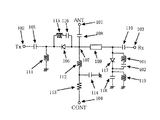
図10は、従来の技術による送受切替スイッチ(詳細は特許公報第2822824号を参照)の構成を示す図である。
【0003】
図に示すように、従来の送受切替スイッチにおいて、送信回路Txはコンデンサ701を介して、第1のダイオード702のアノードに接続され、第1のダイオード702のアノードは、チョークコイルとして働く第1のストリップライン703およびコンデンサ704を介して接地される。さらに、第1のストリップライン703とコンデンサ704の中間点は抵抗705を関して第1のコントロール端子706に接続される。また、第1のダイオード702のカソードはコンデンサ707を介してアンテナANTに接続される。アンテナANTには第2のストリップライン708が接続され、第2のストリップライン708はコンデンサ709を介して受信回路Rxに接続される。また、第2のストリップライン708とコンデンサ709の中間点は第2のダイオード710とコンデンサ711との直列回路を介して接地される。
【0004】
さらに、第1のダイオード702に並列にインダクタ712とコンデンサ713の直列回路が接続され、第1のダイオード702に、つまりインダクタ712とコンデンサ713の直列回路に並列に抵抗714が接続される。さらに、第2のダイオード710に並列に別の抵抗715が接続され、この抵抗715は抵抗716を介して第2のコントロール端子717に接続される。したがって、第2のコントロール端子717は第2のダイオード710のカソード側に接続される。
【0005】
このような構成を有する、従来の技術による送受切替スイッチの動作を以下に説明する。
【0006】
この送受切替スイッチにおいて送信を行う場合、第1のコントロール端子706に正の電圧が印加され、第1、及び第2のダイオード702、710に順方向の電圧が印加されON状態となり、送信回路Txからの送信信号はアンテナANTから送信される。一方、第2のストリップライン708が第2のダイオード710により接地されて共振し、そのインピーダンスが無限大となるため、送信信号は受信回路Rxには伝達されない。
【0007】
次に、この送受切替スイッチにおいて受信を行う場合、第1のコントロール端子706の電圧印加が停止され、第2のコントロール端子717に正の電圧が印加される。第2のコントロール端子717に加えられた電圧は抵抗714、715などで分圧され、第1、及び第2のダイオード702、710に逆方向の電圧として印加されるため、第1、及び第2のダイオード702、710は確実にOFF状態となり、受信回路Rxに受信信号が伝達される。
【0008】
ところで、上記の受信の動作において、ダイオードにはキャパシタンス分が存在するため、受信信号が送信回路Tに漏れる場合がある。これに対し、この送受切替スイッチは、第1のダイオード702のキャパシタンス分とインダクタ712とで並列共振回路を形成することにより、送信回路TxとアンテナANTとの間のアイソレーションを良好にするとともに、第2のコントロール端子717に正の電圧を印加することにより、確実に第1のダイオード702をOFF状態とするようにしている。そのため、第1のダイオード702のキャパシタンス分にばらつきが発生せず、安定した共振周波数を得ることができ、送信回路TxとアンテナANTとの間のアイソレーションを確実なものにすることができ、アンテナANTと受信回路Rxとの間の挿入損失を小さくすることができる。
【0009】
【発明が解決しようとする課題】
従来の送受切替スイッチの構成および動作は以上のようなものであるが、しかしながら、このような従来の送受切替スイッチにおいては、受信時において、抵抗分圧を用いることで、第2のコントロール端子717から第1のダイオード702にも逆バイアス電圧を印加するようにしている。
【0010】
このため、受信の損失への寄与が大きい第2のダイオード710に十分な逆バイアス電圧が与えられず、受信の損失が大きくなってしまうという課題があった。
【0011】
本発明は、従来のこのような課題を解決するものであり、受信時におけるダイオードへ十分な逆バイアス電圧を与えることのできる構成とすることにより、送信の特性を保持したままで、受信の損失を少なくできる送受切替スイッチを提供することを目的とする。
【0012】
【課題を解決するための手段】
上記の目的を達成するために、第1の本発明(請求項1に対応)はアンテナと接続されるアンテナ端子と、送信回路と接続される送信端子と、受信回路と接続される受信端子と、電圧を印加するための一つのコントロール端子と、前記送信端子側にカソードが接続され、前記アンテナ端子側、及び前記コントロール端子側にアノードが接続される第1のダイオードと、前記アンテナ端子と前記受信端子との間に接続されるストリップ線路と、前記ストリップ線路と前記受信端子との間にアノードが接続され、カソードが接地される第2のダイオードとにより構成され、前記一つのコントロール端子と前記接地との間に、前記第1及び第2のダイオードが前記一つのコントロール端子から並列に直流的に接続され、前記一つのコントロール端子から前記第1のダイオードおよび前記第2のダイオードに同時にバイアス電圧を与えることにより、両方をオン、または両方をオフにする電圧が供給されることを特徴とする送受切替スイッチである。
【0013】
また、第2の本発明(請求項2に対応)は、送信時には、前記コントロール端子には正の前記バイアス電圧が印加され、また受信時には、前記コントロール端子に負の前記バイアス電圧が印加されることを特徴とする上記本発明である。
【0014】
また、第3の本発明(請求項5に対応)は、アンテナと接続されるアンテナ端子と、送信回路と接続される送信端子と、受信回路と接続される受信端子と、
電圧を印加するための第1のコントロール端子と、電圧を印加するための第2のコントロール端子と、前記アンテナ端子側、及び前記第1のコントロール端子側にアノードが接続され前記送信端子側、及び前記第2のコントロール端子にカソードが接続される第1のダイオードと、前記アンテナ端子と前記受信端子の間に接続されるストリッブ線路と、前記ストリップ線路と前記受信端子との間にアノードが接続され、カソードが前記第2のコントロール端子に接続される第2のダイオードとにより構成され、前記第1のコントロール端子と前記第2のコントロール端子との間に、前記第1及び第2のダイオードが並列に直流的に接続され、前記第1のコントロール端子に印加される電圧と前記第2のコントロール端子に印加される電圧との差により同時にバイアス電圧を与えることにより、前記第1のダイオード及び前記第2のダイオードの両方をオン、または両方をオフにする電圧が供給されることを特徴とする送受切替スイッチである。
【0015】
また、第4の本発明(請求項6に対応)は、送信時には、前記第1のコントロール端子に正の電圧が印加されるとともに、前記第2のコントロール端子に電圧が印加されないかあるいは負の前記バイアス電圧が印加され、受信時には、前記第1のコントロール端子に電圧が印加されないか、あるいは負の電圧が印加されるとともに、前記第2のコントロール端子に正の前記バイアス電圧が印加されることを特徴とする上記本発明である。
【0017】
また、第5の本発明(請求項8に対応)は、前記コントロール端子に印加される負の前記バイアス電圧は、前記第2のダイオードのQ値を、負の前記バイアス電圧を印加しないとき、あるいは零電圧のときのQ値に比べ1.5倍程度以上とするよう設定されていることを特徴とする上記本発明である。
【0018】
また、第6の本発明(請求項9に対応)はアンテナと接続されるアンテナ端子と、 送信回路と接続される送信端子と、受信回路と接続される受信端子と、
電圧を印加するための一つのコントロール端子と、前記送信端子側にアノードが接続され、前記アンテナ端子側、及び前記一つのコントロール端子側にカソードが接続される第1のダイオードと、前記アンテナ端子と前記受信端子との間に接続されるストリップ線路と、前記ストリップ線路と前記受信端子との間にカソードが接続され、アノードが接地される第2のダイオードとにより構成され、前記一つのコントロール端子と前記接地との間に、前記第1及び第2のダイオードが前記一つのコントロール端子から並列に直流的に接続され、前記一つのコントロール端子から前記第1のダイオード及び前記第2のダイオードに同時にバイアス電圧を与えることにより、両方をオン、または両方をオフにする電圧が供給されることを特徴とする送受切替スイッチである。
【0019】
また、第7の本発明(請求項10に対応)は、送信時には、前記コントロール端子には負の前記バイアス電圧が印加され、また受信時には、前記コントロール端子に正の前記バイアス電圧が印加されることを特徴とする上記本発明である。
【0020】
また、第8の本発明(請求項13に対応)は、アンテナと接続されるアンテナ端子と、送信回路と接続される送信端子と、受信回路と接続される受信端子と、
電圧を印加するための第1のコントロール端子と、電圧を印加するための第2のコントロール端子と、前記アンテナ端子側、及び前記第1のコントロール端子側にカソードが接続され前記送信端子側、及び前記第2のコントロール端子にアノードが接続される第1のダイオードと、前記アンテナ端子と前記受信端子の間に接続されるストリップ線路と、前記ストリップ線路と前記受信端子との間にカソードが接続され、アノードが前記第2のコントロール端子に接続される第2のダイオードとにより構成され、前記第1のコントロール端子と前記第2のコントロール端子との間に、前記第1及び第2のダイオードが並列に直流的に接続され、前記第1のコントロール端子に印加される電圧と前記第2のコントロール端子に印加される電圧との差により同時にバイアス電圧を与えることにより、前記第1のダイオード及び前記第2のダイオードの両方をオン、または両方をオフにする電圧が供給されることを特徴とする送受切替スイッチである。
【0021】
また、第9の本発明(請求項14に対応)は、送信時には、前記第1のコントロール端子に負の前記バイアス電圧が印加されるとともに、前記第2のコントロール端子に電圧が印加されないかあるいは正の前記バイアス電圧が印加され、受信時には、前記第1のコントロール端子に電圧が印加されないか、あるいは正の前記バイアス電圧が印加されるとともに、前記第2のコントロール端子に負の前記バイアス電圧が印加されることを特徴とする上記本発明である。
【0023】
また、第10の本発明(請求項16に対応)は、前記コントロール端子に印加される正の前記バイアス電圧は、前記第2のダイオードのQ値を、正の前記バイアス電圧を印加しないとき、あるいは零電圧のときのQ値に比べ1.5倍程度以上とするよう設定されていることを特徴とする上記本発明である。
【0024】
以上のような本発明の送受切替スイッチは、アンテナ端子と受信端子との間を接地するダイオードに十分な逆バイアス電圧を与えることを特徴とする。
【0025】
【発明の実施の形態】
以下、本発明における送受切替スイッチの実施の形態について、図面を参照しながら説明する。
(第1の実施の形態)
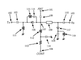
図1は、本発明における第1の実施の形態の送受切替スイッチを示す図である。図において、送受切替スイッチは、アンテナ端子101はアンテナANTに接続され、送信端子102は送信回路Txに接続され、受信端子103は受信回路Rxに接続され、コントロール端子104は切替制御を行うコントロール回路CONTに接続される。送信端子102はコンデンサ105を介して第1のダイオード106のカソードに接続され、第1のダイオード106のアノードは、接続点107、コンデンサ108を介してアンテナ端子101に接続される。また、アンテナ端子101は、コンデンサ108、接続点107、ストリップ線路109、コンデンサ110を介して受信端子103に接続される。また、第1のダイオード106のカソードは、インダクタ111を介して接地される。第1のダイオード106のアノードは接続点107、インダクタ112、抵抗113を介してコントロール端子104に接続され、インダクタ112と抵抗113の中間にはコンデンサ114を介して接地される。
【0026】
さらに、第1のダイオード106に並列にインダクタ115とコンデンサ116の直列回路が接続される。また、ストリップ線路109とコンデンサ110の中間には第2のダイオード117のアノードが接続され、第2のダイオード117のカソードはコンデンサ118、及びインダクタ119を並列に介して接地されている。
【0027】
以上のような構成を有する本実施の形態の送受切替スイッチの動作について、以下、説明を行う。
【0028】
はじめに、送信回路に接続する動作を説明する。送受切替スイッチにおいて、送信回路TxとアンテナANTを接続する場合、コントロール回路CONTからコントロール端子104に第1、及び第2のダイオード106、117を動作させる正の電圧が与えられる。このときコントロール端子104から与えられた正の電圧はコンデンサ105、108、110、114、116、118により直流カットされ、第1のダイオード106、インダクタ111、112、抵抗113を含む回路、及び第2のダイオード117、ストリップ線路109、インダクタ112、119、抵抗113を含む回路のみ正の電圧が与えられ、第1、及び第2のダイオード106、117はON状態となる。
【0029】
上記の状態において、第1のダイオード106がONとなることにより、送信端子102とアンテナ端子101間のインピーダンスが低くなり接続される。このとき、第1のダイオード106のカソードはインダクタ111を介して接地されているが、送信周波数において十分高いインピーダンスとすることにより、インダクタ111がチョークコイルとして働くため、高周波的には接地の影響がない状態となる。
【0030】
また、第2のダイオード117がONとなることにより、ストリップ線路109は高周波的に接地されて共振するため、接続点107から受信端子103側を見たインピーダンスが非常に大きくなり、受信回路Rxには送信端子102からの信号は伝達されない。
【0031】
ところで、送信時においては第1と第2のダイオード106、117はON状態となるが、このときこれらのダイオードにはインダクタンス成分が存在し、接続点107から受信回路Rxを見たインピーダンスが十分大きくできない。
【0032】
そこで本実施の形態では、第2のダイオード117のカソードをコンデンサ118を介して接地することにより、第2のダイオード117のインダクタンス成分とコンデンサ118とで直列共振回路を形成し、接続点107から受信回路Rxを見たインピーダンスが十分大きくなるようにした。これにより、送信回路Txからの信号が受信回路Rxに漏れることなく、送信回路TxとアンテナANTの挿入損失を小さくできる。
【0033】
次に、受信回路に接続する動作を説明する。送受切替スイッチにおいて、アンテナANTと受信回路Rxを接続する場合、コントロール回路CONTからコントロール端子104に第1、及び第2のダイオード106、117をOFFとする負の電圧が与えられ、第1、及び第2のダイオード106、117はOFF状態となる。
【0034】
上記の状態において、第1のダイオード106をOFFにすることにより、アンテナ端子101から送信端子102への経路がカットされるとともに、さらに第2のダイオード117がOFFとなることにより、受信端子103とアンテナ端子101間のインピーダンスが低くなり、両者は接続される。
【0035】
このとき、第1、及び第2のダイオード106、117にはキャパシタンス成分が存在するため、アンテナANTからの受信信号が送信回路Txに漏れる場合、さらに、第2のダイオード117が並列に接続されていることによる受信の挿入損失の増加につながる場合がある。
【0036】
しかしながら、本実施の形態の送受切替スイッチにおいては、第1のダイオード106と並列にインダクタ115が接続されているため、第1のダイオード106のキャパシタンス成分とインダクタ115で並列共振回路が形成され、接続点107から送信回路側を見たインピーダンスは非常に大きくなり、アンテナANTからの受信信号は送信回路Txに漏れることなく受信回路Rxに伝達される。
【0037】
さらに、第2のダイオード117に関しては、第1のダイオード106と並列に接続されており、コントロール端子104からの負の電圧が分圧することなく印加されるため、十分な逆バイアス電圧が与えられているので、第2のダイオード117での損失を最小限に抑え、受信の挿入損失を改善することができる。
【0038】
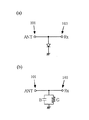
ここで、第2のダイオード117の動作について詳細な説明を行う。第2のダイオードのみについて考えると、図2(a)に示すように、受信時には第2のダイオード117が並列に接地されている構成となり、その等価回路は、簡易的にコンダクタンスGとサセプタンスBにより図2(b)のように表せる。
【0039】
この第2のダイオードに逆バイアス電圧を与えることにより、そのインピーダンスは逆バイアス電圧の大きさによって変化する、すなわち第2のダイオードのQ値が変化する。この場合、Q値はQ=B/Gで表される。
【0040】
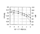
また図3に示すのは、2GHz帯の周波数における第2のダイオードに与える逆バイアス電圧の大きさとQ値、及びアンテナ端子101と受信端子103間の損失との関係である。図3において、横軸は逆バイアス電圧、縦軸はQ値、及び損失である。逆バイアス電圧が大きいほど第2のダイオード117のQ値はおおきくなり、また、アンテナ端子101と受信端子103間の損失は小さくなっている。すなわち、逆バイアス電圧が大きいほど受信時の損失は改善できる。図3においては、第2のダイオード117における零電圧時のQ値の1.5倍程度となる−1.5Vの逆バイアス電圧を与えることによりアンテナ端子101と受信端子103間損失がおおよそ0.1dB改善されている。
【0041】
次に、図4に、本発明における第1の実施の形態の送受切替スイッチの第2の構成例を示す。図に示すように、本実施の形態の送受切替スイッチの第2の構成例は、上述した第1の構成例と比較して、第1および第2のダイオードの極性がそれぞれ反転している点において異なる。すなわち、図に示すように、送受切替スイッチにおいて、送信端子102はコンデンサ105を介して第1のダイオード106のアノードに接続され、第1のダイオード106のカソードは、接続点107、コンデンサ108を介してアンテナ端子101に接続される。また、第1のダイオード106のアノードは、インダクタ111を介して接地される。第1のダイオード106のカソードは接続点107、インダクタ112、抵抗113を介してコントロール端子104に接続され、インダクタ112と抵抗113の中間にはコンデンサ114を介して接地される。
【0042】
このような構成を有する本実施の形態の第2の構成例の動作は、以下の通りである。すなわち、送信回路TxとアンテナANTを接続する場合は、コントロール回路CONTからコントロール端子104に第1、及び第2のダイオード106、117を動作させる負の電圧が与えられ、第1のダイオード106がONとなることにより、送信端子102とアンテナ端子101間のインピーダンスが低くなり接続される。また、この場合も上述第1例と同様、第2のダイオード117がONとなることにより、ストリップ線路109は高周波的に接地されて共振するため、接続点107から受信端子103側を見たインピーダンスが非常に大きくなり、受信回路Rxには送信端子102からの信号は伝達されない。
【0043】
次に、アンテナANTと受信回路Rxを接続する場合、コントロール回路CONTからコントロール端子104に第1、及び第2のダイオード106、117をOFFとする正の電圧が与えられ、第2のダイオード117がOFFとなることにより、受信端子103とアンテナ端子101間のインピーダンスが低くなり、両者は接続される。さらに、上述第1例と同様、第2のダイオード117は第1のダイオード106と並列に接続されており、コントロール端子104からの正の電圧が分圧することなく印加されるため、十分な逆バイアス電圧が与えられているので、第2のダイオード117での損失を最小限に抑え、受信の挿入損失を改善することができる。
【0044】
このように、本発明における第1の実施の形態の送受切替スイッチは、アンテナと接続されるアンテナ端子と、送信回路と接続される送信端子と、受信回路と接続される受信端子と、前記送信端子側にカソードが接続され前記アンテナ端子側、及びコントロール端子側にアノードが接続される第1のダイオードと、前記アンテナ端子と前記受信端子の間に接続されるストリップ線路と、前記ストリップ線路と前記受信端子との間にアノードが接続されカソードが接地される第2のダイオードとにより構成され、第1、及び第2のダイオード106、117に与えられる逆バイアス電圧を大きくすることができ、それにより、受信時の損失を改善できるものである。
【0045】
なお、本発明の第1の実施の形態で示した図3の特性は、使用するダイオードにより異なるものであり、逆バイアス電圧の大きさ、及び改善量は本実施例の値とは異なるが、逆バイアス電圧を与えてQ値を大きくすることによる受信時の低損失化の効果に関しては同様である。
【0046】
また、ストリップ線路は送信周波数に関して、波長λの1/4の長さが理想的であり、分布定数回路、あるいは集中定数回路により構成されていてもかまわない。また、インダクタ111、112、115、119はコイル、もしくはストリップ線路により形成されてもかまわないが、これらのインダクタに関しては、損失を考慮するとQ値の高いものを用いるのが望ましい。
【0047】
また、第1のダイオード106に並列に接続されるインダクタ115には、インダクタ115を介して直接電流が流れることを防ぐためにコンデンサ116が直列に接続されているが、これらの値は、第1のダイオード106のキャパシタンス成分と、インダクタ115とコンデンサ116の直列回路との並列共振を与える値に設定すればよい。
【0048】
また、第2のダイオード117のカソード(第2の構成例ではアノード)はコンデンサ118とインダクタ119を介して並列に接地されているが、このインダクタ119は第2のダイオード117の直流電流経路を確保するものであり、これらの値は、第2のダイオード117がON状態にある場合は、第2のダイオード117のインダクタンス成分と、コンデンサ118とインダクタ119の並列回路の直列共振を与える値に設定すればよい。
【0049】
また、図5に示すように、第2のダイオード117のアノードとカソードとをインダクタ401、コンデンサ402を介して接続してもよい。この場合は、受信時、すなわち第2のダイオード117のOFF状態のキャパシタンス成分と、インダクタ401とコンデンサ402との直列回路とにより並列共振回路が形成され、さらなる低損失化の効果が実現できるものである。
(第2の実施の形態)
図6は、本発明における第2の実施の形態の送受切替スイッチを示す図である。
【0050】
図6において、送受切替スイッチは、アンテナ端子101はアンテナANTに接続され、送信端子102は送信回路Txに接続され、受信端子103は受信回路Rxに接続され、第1のコントロール端子501は切替制御を行うコントロール回路CONT1に接続され、第2のコントロール端子502は切替制御を行うコントロール回路CONT2に接続される。送信端子102はコンデンサ105を介して第1のダイオード106のカソードに接続され、第1のダイオード106のアノードは、接続点107、コンデンサ108を介してアンテナ端子101に接続される。また、アンテナ端子101は、コンデンサ108、接続点107、ストリップ線路109、コンデンサ110を介して受信端子103に接続される。また、第1のダイオード106のカソードは、インダクタ503、抵抗504を介して第2のコントロール端子502に接続され、インダクタ503と抵抗504の中間にはコンデンサ505を介して接地される。第1のダイオード106のアノードは接続点107、インダクタ112、抵抗113を介して第1のコントロール端子501に接続され、インダクタ112と抵抗113の中間にはコンデンサ114を介して接地される。
【0051】
さらに、第1のダイオード106に並列にインダクタ115とコンデンサ116の直列回路が接続される。また、ストリップ線路109とコンデンサ110の中間には第2のダイオード117のアノードが接続され、第2のダイオード117のカソードはインダクタ506、抵抗507を介して第2のコントロール端子502に接続され、インダクタ506と抵抗507の中間にはコンデンサ508を介して接地されている。
【0052】
以上のような構成を有する本実施の形態の送受切替スイッチの動作について、以下、説明を行う。
【0053】
はじめに、送信回路に接続する動作を説明する。送受切替スイッチにおいて、送信回路TxとアンテナANTを接続する場合、第1のコントロール回路CONT1から第1のコントロール端子501には、第1、及び第2のダイオード106、117を動作させる正の電圧が与えられ、また、第2のコントロール回路CONT2から第2のコントロール端子502には電圧が停止、あるいは零電圧、もしくは負の電圧が与えられる。
【0054】
このとき、第1のコントロール端子501から与えられた正の電圧は、コンデンサ105、108、110、114、116、505、508により直流カットされ、第1のダイオード106、インダクタ112、503、抵抗113、504を含む回路、及び第2のダイオード117、ストリップ線路109、インダクタ112、506、抵抗113、507を含む回路のみ正の電圧が与えられ、第1、及び第2のダイオード106、117はON状態となる。
【0055】
上記の状態において、第1のダイオード106がONとなることにより、送信端子102とアンテナ端子101間のインピーダンスが低くなり接続される。このとき、第1のダイオード106のカソードはインダクタ503を介して第2のコントロール端子502に接続されているが、送信周波数において十分高いインピーダンスとすることにより、インダクタ503はチョークコイルとして働くため、高周波的には送信端子102とアンテナ端子101との経路には影響がない状態となる。
【0056】
また、第2のダイオード117がONとなることにより、ストリップ線路109は高周波的に接地されて共振するため、接続点107から受信端子103側を見たインピーダンスが非常に大きくなり、受信回路Rxには送信端子102からの信号は伝達されない。
【0057】
ところで、送信時においては第1と第2のダイオード106、117はON状態となるが、このときこれらのダイオードにはインダクタンス成分が存在し、接続点107から受信回路Rxを見たインピーダンスが十分大きくできない。
【0058】
そこで本実施の形態では、第2のダイオード117のカソードをコンデンサ508を介して接地することにより、第2のダイオード117のインダクタンス成分とコンデンサ508とで直列共振回路を形成し、接続点107から受信回路Rxを見たインピーダンスが十分大きくなるようにした。これにより、送信回路Txからの信号が受信回路Rxに漏れることなく、送信回路TxとアンテナANTの挿入損失を小さくできる。
【0059】
次に、受信回路に接続する動作を説明する。送受切替スイッチにおいて、アンテナANTと受信回路Rxを接続する場合、第1のコントロール回路CONT1から第1のコントロール端子501に第1、及び第2のダイオード106、117をOFFとする負の電圧が与えられ、また、第2のコントロール回路CONT2から第2のコントロール端子502には電圧が停止、あるいは零電圧、もしくは正の電圧が与えられ、第1、及び第2のダイオード106、117はOFF状態となる。
【0060】
上記の状態において、第1のダイオード106をOFFにすることにより、アンテナ端子101から送信端子102への経路がカットされるとともに、さらに第2のダイオード117がOFFとなることにより、受信端子103とアンテナ端子101間のインピーダンスが低くなり、両者は接続される。
【0061】
このとき、第1、及び第2のダイオード106、117にはキャパシタンス成分が存在するため、アンテナANTからの受信信号が送信回路Txに漏れる場合、さらに、第2のダイオード117が並列に接続されていることによる受信時の挿入損失の増加につながる。
【0062】
しかしながら、本実施の形態の送受切替スイッチにおいては、第1のダイオード106と並列にインダクタ115が接続されているため、第1のダイオード106のキャパシタンス成分とインダクタ115で並列共振回路が形成され、接続点107から送信回路側を見たインピーダンスは非常に大きくなり、アンテナANTからの受信信号は送信回路Txに漏れることなく受信回路Rxに伝達される。
【0063】
さらには、第2のダイオード117に関しては、第1のダイオード106と並列に接続されており、コントロール端子501からの負の電圧が分圧することなく印加されるため、十分な逆バイアス電圧が与えられているので、第2のダイオード117での損失を最小限に抑え、受信の挿入損失を改善することができる。
【0064】
以上説明した、本発明の第2の実施の形態の動作および効果は第1の実施の形態と同様であるが、本発明の第2の実施の形態において、第1の実施の形態と異なるのは、第1、及び第2のダイオード106,107のカソード側が第2のコントロール端子502に接続されている点である。これにより、受信時には、第1のコントロール端子501の電圧を停止、もしくは零電圧とし、第2のコントロール端子502の電圧を正の電圧とすることにより、第1の実施の形態とは異なり、負の電圧を用いることなく、第2のダイオード117に十分な逆バイアス電圧を与えることができる。
【0065】
なお、本実施の形態も、第1の実施の形態の第2構成例と同様、第2構成例として、第1および第2のダイオードの極性をそれぞれ反転させたものを用いることができる。
【0066】
図7は、本発明の第2の実施の形態の第2構成例を示す図である。図に示すように、送受切替スイッチにおいて、送信端子102はコンデンサ105を介して第1のダイオード106のアノードに接続され、第1のダイオード106のカソードは、接続点107、コンデンサ108を介してアンテナ端子101に接続される。また、第1のダイオード106のアノードは、インダクタ503、抵抗504を介して第2のコントロール端子502に接続され、インダクタ503と抵抗504の中間にはコンデンサ505を介して接地される。第1のダイオード106のカソードは接続点107、インダクタ112、抵抗113を介して第1のコントロール端子501に接続され、インダクタ112と抵抗113の中間にはコンデンサ114を介して接地される。
【0067】
さらに、ストリップ線路109とコンデンサ110の中間には第2のダイオード117のカソードが接続され、第2のダイオード117のアノードはインダクタ506、抵抗507を介して第2のコントロール端子502に接続され、インダクタ506と抵抗507の中間にはコンデンサ508を介して接地されている。
【0068】
このような構成を有する本発明の第2の実施の形態の第2構成例の動作は、送信回路Txと接続する場合は、第1のコントロール回路CONT1から第1のコントロール端子501には、第1、及び第2のダイオード106、117を動作させる負の電圧を与えるとともに、第2のコントロール回路CONT2から第2のコントロール端子502には電圧が停止、あるいは零電圧、もしくは正の電圧が与えることにより動作が行われ、また、受信回路Rxと接続する場合は、第1のコントロール回路CONT1から第1のコントロール端子501に第1、及び第2のダイオード106、117をOFFとする正の電圧が与えられ、また、第2のコントロール回路CONT2から第2のコントロール端子502には電圧が停止、あるいは零電圧、もしくは負の電圧が与えられることにより動作が行われ、いずれの場合においても、上述の第1構成例と同様の作用、効果を奏する。
(第3の実施の形態)
図8は、本発明における第3の実施の形態の送受切替スイッチを示す図である。
【0069】
図において、送受切替スイッチは、アンテナ端子101はアンテナANTに接続され、送信端子102は送信回路Txに接続され、受信端子103は受信回路Rxに接続され、コントロール端子104は切替制御を行うコントロール回路CONTに接続される。送信端子102はコンデンサ105を介して第1のダイオード106のアノードに接続され、第1のダイオード106のカソードは、接続点107、コンデンサ108を介してアンテナ端子101に接続される。また、アンテナ端子101は、コンデンサ108、接続点107、ストリップ線路109、コンデンサ110を介して受信端子103に接続される。また、第1のダイオード106のアノードはインダクタ601、抵抗602を介してコントロール端子104に接続され、インダクタ601と抵抗602の中間にはコンデンサ603を介して接地される。さらに、第1のダイオード106に並列にインダクタ115とコンデンサ116の直列回路が接続される。
【0070】
また、ストリップ線路109とコンデンサ110の中間には第2のダイオード117のアノードが接続され、第2のダイオード117のカソードはコンデンサ118、及びインダクタ119を並列に介して接地されている。
【0071】
以上のような構成を有する本実施の形態の送受切替スイッチの動作について、以下、説明を行う。
【0072】
はじめに、送信回路に接続する動作を説明する。送受切替スイッチにおいて、送信回路TxとアンテナANTを接続する場合、コントロール回路CONTからコントロール端子104に第1、及び第2のダイオード106、117を動作させる正の電圧が与えられる。
【0073】
このとき、コントロール端子104から与えられた正の電圧はコンデンサ105、108、110、116、118、603により直流カットされ、第1、及び第2のダイオード106、117、インダクタ601、119、抵抗602、ストリップ線路109を含む回路のみ正の電圧が与えられ、第1、及び第2のダイオード106、117はON状態となる。
【0074】
上記の状態において、第1のダイオード106がONとなることにより、送信端子102とアンテナ端子101間のインピーダンスが低くなり接続される。このとき、第1のダイオード106のアノードはインダクタ601を介してコントロール端子104に接続されているが、送信周波数において十分高いインピーダンスとすることにより、インダクタ601はチョークコイルとして働くため、高周波的には送信端子102とアンテナ端子101との経路には影響がない状態となる。
【0075】
また、第2のダイオード117がONとなることによりストリップ線路109は高周波的に接地されて共振するため、接続点107から受信端子103側を見たインピーダンスが非常に大きくなり、受信回路Rxには送信端子102からの信号は伝達されない。
【0076】
ところで、送信時においては第1と第2のダイオード106、117はON状態となるが、このときこれらのダイオードにはインダクタンス成分が存在し、接続点107から受信回路Rxを見たインピーダンスが十分大きくできない。
【0077】
そこで本実施の形態では、第2のダイオード117のカソードをコンデンサ118を介して接地することにより、第2のダイオード117のインダクタンス成分とコンデンサ118とで直列共振回路を形成し、接続点107から受信回路Rxを見たインピーダンスが十分大きくなるようにした。これにより、送信回路Txからの信号が受信回路Rxに漏れることなく、送信回路TxとアンテナANTの挿入損失を小さくできる。
【0078】
次に、受信回路に接続する動作を説明する。送受切替スイッチにおいて、アンテナANTと受信回路Rxを接続する場合、コントロール回路CONTからコントロール端子104に第1、及び第2のダイオード106、117をOFFとする負の電圧が与えられ、第1、及び第2のダイオード106、117はOFF状態となり、特に、第1のダイオード106をOFFにすることにより、アンテナ端子101から送信端子102への経路がカットされるとともに、さらに第2のダイオード117がOFFとなることにより、受信端子103とアンテナ端子101間のインピーダンスが低くなり、両者は接続される。
【0079】
このとき、第1、及び第2のダイオード106、117にはキャパシタンス成分が存在するため、アンテナANTからの受信信号が送信回路Txに漏れる場合、さらに、第2のダイオード117が並列に接続されていることによる受信時の挿入損失の増加につながる場合がある。
【0080】
しかしながら、本実施の形態の送受切替スイッチにおいては、第1または第2の実施の形態と同様、第1のダイオード106と並列にインダクタ115が接続されているため、第1のダイオード106のキャパシタンス成分とインダクタ115で並列共振回路が形成され、接続点107から送信回路側を見たインピーダンスは非常に大きくなり、アンテナANTからの受信信号は送信回路Txに漏れることなく受信回路Rxに伝達される。
【0081】
ここで、本実施の形態において、第1の実施の形態と異なるのは、第1の実施の形態においては第1、及び第2のダイオード106、117はコントロール端子104に並列に接続される構成となっているが、第3の実施の形態においては第1、及び第2のダイオード106、117はコントロール端子104に直列に接続される構成となっている。この場合、受信時に第2のダイオード117に与えられる逆バイアス電圧は第1のダイオード106と第2のダイオード117との直列接続により分圧となるが、第2のダイオード117に逆バイアスを与えることにより、第2のダイオード117のQ値を向上して受信時の損失を改善するという効果は第1の実施の形態と同様である。
【0082】
したがって、第2のダイオード117に関しては、十分な逆バイアス電圧が与えられているため、第2のダイオード117での損失を最小限に抑え、受信の挿入損失を改善することができる。
【0083】
なお、本実施の形態も、第1および第2の実施の形態のそれぞれの第2構成例と同様、第2構成例として、第1および第2のダイオードの極性をそれぞれ反転させたものを用いることができる。
【0084】
図9は、本発明の第3の実施の形態の第2構成例を示す図である。図に示すように、送受切替スイッチにおいて、送信端子102はコンデンサ105を介して第1のダイオード106のカソードに接続され、第1のダイオード106のアノードは、接続点107、コンデンサ108を介してアンテナ端子101に接続される。また、第1のダイオード106のカソードはインダクタ601、抵抗602を介してコントロール端子104に接続される。また、ストリップ線路109とコンデンサ110の中間には第2のダイオード117のカソードが接続され、第2のダイオード117のアノードはコンデンサ118、及びインダクタ119を並列に介して接地されている。
【0085】
このような構成を有する本発明の第3の実施の形態の第2構成例の動作は、送信回路Txと接続する場合は、コントロール回路CONTからコントロール端子104に第1、及び第2のダイオード106、117を動作させる負の電圧が与えられて接続動作が行われ、受信回路Rxと接続する場合は、コントロール回路CONTからコントロール端子104に第1、及び第2のダイオード106、117をOFFとする正の電圧が与えられ、第1のダイオード106をOFFにすることにより、アンテナ端子101から送信端子102への経路がカットされるとともに、さらに第2のダイオード117がOFFとなることにより、受信端子103とアンテナ端子101間のインピーダンスが低くなり、両者は接続される。送信回路Tx、受信回路Rxいずれの回路と接続する場合の動作でも、上述の第1構成例と同様の作用、効果を奏する。
【0086】
なお、本発明の第1および第3の実施の形態においては、特にスイッチ切替のためのコントロール端子を一つとしたことで、従来例よりも構成を単純化して、回路を小型化できる効果がある。
【0087】
以上の構成とすることにより、本発明の送受切替スイッチは、受信時におけるダイオードへ十分なバイアス電圧を与えることのできる構成とすることにより、送信の特性を保持したままで、受信の損失を少なくできる送受切替スイッチを提供することを目的とする。
【0088】
以上説明したように本発明の送受切替スイッチは、アンテナと接続されるアンテナ端子と、送信回路と接続される送信端子と、受信回路と接続される受信端子と、前記送信端子側にカソードが接続され前記アンテナ端子側、及びコントロール端子側にアノードが接続される第1のダイオードと、前記アンテナ端子と前記受信端子の間に接続されるストリップ線路と、前記ストリップ線路と前記受信端子との間にアノードが接続されカソードが接地される第2のダイオードとにより構成され、受信時におけるダイオードへ十分な逆バイアス電圧を与え、第2のダイオードのQ値を向上させることにより、第2のダイオードが並列接続されることによる受信時の損失を改善することができる。
【0089】
【発明の効果】
以上述べたところから明らかなように本発明は、送受切替スイッチにおいて、送信時の特性を保持したままで、受信時の挿入損失を改善できるという効果がある。
【図面の簡単な説明】
【図1】本発明における第1の実施の形態の送受切替スイッチの構成図
【図2】(a)ダイオードの並列接地の図
(b)ダイオードのOFF時における並列接地の簡易等価回路図
【図3】OFF時のダイオードのQ値、及び並列接地時の損失と逆バイアス電圧特性を示す図
【図4】本発明における第1の実施の形態の送受切替スイッチの第2例の構成図
【図5】本発明における第1の実施の形態の送受切替スイッチの構成の別の形態図
【図6】本発明における第2の実施の形態の送受切替スイッチの構成図
【図7】本発明における第1の実施の形態の送受切替スイッチの第2例の構成図
【図8】本発明における第3の実施の形態の送受切替スイッチの構成図
【図9】本発明における第3の実施の形態の送受切替スイッチの第2例の構成図
【図10】従来の送受切替スイッチの構成図
【符号の説明】
101 アンテナ端子
102 送信端子
103 受信端子
104 コントロール端子
105、108、110、114、116、118、402、505、508、603、701、704、707、709、711、713 コンデンサ
106、702 第1のダイオード
107 接続点
109 ストリップ線路
111、112、115、119、401、503、506、601、712
インダクタ
113、504、507、602、705、714、715、716 抵抗
117、710 第2のダイオード
501、706 第1のコントロール端子
502、717 第2のコントロール端子
703 第1のストリップライン
708 第2のストリップライン[0001]
TECHNICAL FIELD OF THE INVENTION
The present invention relates to a transmission / reception switch used for switching a signal transmission line in a high-frequency circuit such as a wireless device or a portable terminal device.
[0002]
[Prior art]
FIG. 10 is a diagram showing a configuration of a transmission / reception changeover switch according to a conventional technique (for details, see Japanese Patent Publication No. 2822824).
[0003]
As shown in the figure, in the conventional transmission / reception changeover switch, the transmission circuit Tx is connected to the anode of the
[0004]
Further, a series circuit of an
[0005]
The operation of the conventional transmission / reception changeover switch having such a configuration will be described below.
[0006]
When transmission is performed by the transmission / reception switch, a positive voltage is applied to the
[0007]
Next, when receiving is performed by the transmission / reception switch, the application of the voltage to the
[0008]
By the way, in the above-described reception operation, a reception signal may leak to the transmission circuit T because a diode has a capacitance component. On the other hand, this transmission / reception changeover switch improves the isolation between the transmission circuit Tx and the antenna ANT by forming a parallel resonance circuit with the capacitance of the
[0009]
[Problems to be solved by the invention]
The configuration and operation of the conventional transmission / reception changeover switch are as described above. However, in such a conventional transmission / reception changeover switch, the
[0010]
Therefore, there is a problem that a sufficient reverse bias voltage is not applied to the
[0011]
The present invention is to solve such a conventional problem. By adopting a configuration capable of applying a sufficient reverse bias voltage to a diode at the time of reception, loss of reception can be maintained while maintaining transmission characteristics. It is an object of the present invention to provide a transmission / reception switch capable of reducing the number of transmission / reception.
[0012]
[Means for Solving the Problems]
In order to achieve the above object, a first aspect of the present invention (corresponding to claim 1) includes an antenna terminal connected to an antenna, a transmission terminal connected to a transmission circuit, and a reception terminal connected to a reception circuit. For applying voltage One A control terminal, a cathode connected to the transmission terminal side, a first diode connected to the antenna terminal side and an anode connected to the control terminal side, and a first diode connected between the antenna terminal and the reception terminal. An anode is connected between the strip line and the reception terminal, and a second diode is connected to the cathode and the cathode is grounded; Between the one control terminal and the ground, Wherein the first and second diodes are One DC connection from the control terminal in parallel Continued And said One A first terminal and a second diode from a control terminal By applying a bias voltage to A transmission / reception changeover switch to which a voltage for turning on both or turning off both is supplied.
[0013]
According to a second aspect of the present invention (corresponding to claim 2), at the time of transmission, a positive The bias Voltage is applied, and during reception, a negative signal is applied to the control terminal. The bias The present invention is characterized in that a voltage is applied.
[0014]
In a third aspect of the present invention (corresponding to claim 5), an antenna terminal connected to an antenna, a transmission terminal connected to a transmission circuit, a reception terminal connected to a reception circuit,
A first control terminal for applying a voltage, a second control terminal for applying a voltage, the antenna terminal side, and an anode connected to the first control terminal side, the transmission terminal side; A first diode having a cathode connected to the second control terminal; a strip line connected between the antenna terminal and the reception terminal; and an anode connected between the strip line and the reception terminal. And a second diode having a cathode connected to the second control terminal, The first and second diodes are connected in parallel between the first control terminal and the second control terminal in a DC manner, The difference between the voltage applied to the first control terminal and the voltage applied to the second control terminal By applying a bias voltage at the same time , The first diode as well as Turn both of the second diodes on or both off Voltage is supplied This is a transmission / reception switch.
[0015]
Further, in the fourth invention (corresponding to claim 6), at the time of transmission, a positive voltage is applied to the first control terminal and no voltage is applied to the second control terminal or a negative voltage is applied to the second control terminal. The bias A voltage is applied, and at the time of reception, no voltage is applied to the first control terminal or a negative voltage is applied and a positive voltage is applied to the second control terminal. The bias The present invention is characterized in that a voltage is applied.
[0017]
According to a fifth aspect of the present invention (corresponding to claim 8), a negative voltage applied to the control terminal is provided. The bias The voltage changes the Q value of the second diode by a negative value. The bias The present invention is characterized in that it is set to be about 1.5 times or more the Q value when no voltage is applied or at zero voltage.
[0018]
According to a sixth aspect of the present invention (corresponding to claim 9), an antenna terminal connected to an antenna, a transmission terminal connected to a transmission circuit, a reception terminal connected to a reception circuit,
For applying voltage One An anode is connected to the control terminal and the transmission terminal side, the antenna terminal side, and the One A first diode having a cathode connected to the control terminal side, a strip line connected between the antenna terminal and the reception terminal, a cathode connected between the strip line and the reception terminal, and an anode And a second diode grounded, Between the one control terminal and the ground, Wherein the first and second diodes are One DC connection from the control terminal in parallel Continued And said One Control terminal to said first diode as well as The second diode By applying a bias voltage to A transmission / reception changeover switch to which a voltage for turning on both or turning off both is supplied.
[0019]
According to a seventh aspect of the present invention (corresponding to claim 10), at the time of transmission, the control terminal has a negative voltage. The bias Voltage is applied, and during reception, a positive The bias The present invention is characterized in that a voltage is applied.
[0020]
An eighth aspect of the present invention (corresponding to claim 13) includes an antenna terminal connected to an antenna, a transmission terminal connected to a transmission circuit, a reception terminal connected to a reception circuit,
A first control terminal for applying a voltage, a second control terminal for applying a voltage, the antenna terminal side, and a cathode connected to the first control terminal side, the transmission terminal side; A first diode having an anode connected to the second control terminal, a stripline connected between the antenna terminal and the reception terminal, and a cathode connected between the stripline and the reception terminal. A second diode having an anode connected to the second control terminal, The first and second diodes are connected in parallel between the first control terminal and the second control terminal in a DC manner, The difference between the voltage applied to the first control terminal and the voltage applied to the second control terminal By applying a bias voltage at the same time , The first diode as well as Turn both of the second diodes on or both off Voltage is supplied This is a transmission / reception switch.
[0021]
According to a ninth aspect of the present invention (corresponding to claim 14), at the time of transmission, a negative The bias While a voltage is applied, no voltage is applied to the second control terminal or a positive The bias A voltage is applied, and at the time of reception, no voltage is applied to the first control terminal or a positive The bias A voltage is applied and a negative voltage is applied to the second control terminal. The bias The present invention is characterized in that a voltage is applied.
[0023]
According to a tenth aspect of the present invention (corresponding to claim 16), a positive voltage applied to the control terminal is provided. The bias The voltage changes the Q value of the second diode to a positive value. The bias The present invention is characterized in that it is set to be about 1.5 times or more the Q value when no voltage is applied or at zero voltage.
[0024]
The transmission / reception switch of the present invention as described above is characterized in that a sufficient reverse bias voltage is applied to a diode that grounds between an antenna terminal and a reception terminal.
[0025]
BEST MODE FOR CARRYING OUT THE INVENTION
Hereinafter, embodiments of a transmission / reception switch according to the present invention will be described with reference to the drawings.
(First Embodiment)
FIG. 1 is a diagram showing a transmission / reception switch according to the first embodiment of the present invention. In the figure, an
[0026]
Further, a series circuit of an
[0027]
The operation of the transmission / reception switch of the present embodiment having the above configuration will be described below.
[0028]
First, an operation of connecting to the transmission circuit will be described. When the transmission circuit Tx is connected to the antenna ANT in the transmission / reception switch, a positive voltage for operating the first and
[0029]
In the above state, when the
[0030]
In addition, when the
[0031]
By the way, at the time of transmission, the first and
[0032]
Therefore, in the present embodiment, the cathode of the
[0033]
Next, an operation of connecting to the receiving circuit will be described. In the transmission / reception switch, when the antenna ANT is connected to the reception circuit Rx, a negative voltage for turning off the first and
[0034]
In the above state, turning off the
[0035]
At this time, since a capacitance component exists in the first and
[0036]
However, in the transmission / reception switch of the present embodiment, since the
[0037]
Further, the
[0038]
Here, the operation of the
[0039]
By applying a reverse bias voltage to the second diode, its impedance changes according to the magnitude of the reverse bias voltage, that is, the Q value of the second diode changes. In this case, the Q value is represented by Q = B / G.
[0040]
FIG. 3 shows the relationship between the magnitude of the reverse bias voltage applied to the second diode and the Q value at a frequency in the 2 GHz band, and the loss between the
[0041]
Next, FIG. 4 shows a second configuration example of the transmission / reception switch according to the first embodiment of the present invention. As shown in the figure, the second configuration example of the transmission / reception switch according to the present embodiment is different from the first configuration example in that the polarities of the first and second diodes are inverted. In. That is, as shown in the figure, in the transmission / reception changeover switch, the
[0042]
The operation of the second configuration example of the present embodiment having such a configuration is as follows. That is, when the transmission circuit Tx is connected to the antenna ANT, a negative voltage for operating the first and
[0043]
Next, when connecting the antenna ANT and the receiving circuit Rx, a positive voltage for turning off the first and
[0044]
As described above, the transmission / reception switch according to the first embodiment of the present invention includes the antenna terminal connected to the antenna, the transmission terminal connected to the transmission circuit, the reception terminal connected to the reception circuit, and the transmission terminal. A first diode having a cathode connected to a terminal side and an anode connected to the antenna terminal side and the control terminal side; a strip line connected between the antenna terminal and the reception terminal; A second diode whose anode is connected to the receiving terminal and whose cathode is grounded, the reverse bias voltage applied to the first and
[0045]
Note that the characteristics of FIG. 3 shown in the first embodiment of the present invention are different depending on the diode used, and the magnitude of the reverse bias voltage and the amount of improvement are different from the values of the present embodiment. The same applies to the effect of reducing the loss at the time of reception by increasing the Q value by applying a reverse bias voltage.
[0046]
The strip line is ideally の 長 the wavelength λ of the transmission frequency, and may be constituted by a distributed constant circuit or a lumped constant circuit. Further, the
[0047]
A
[0048]
The cathode (anode in the second configuration example) of the
[0049]
Further, as shown in FIG. 5, the anode and the cathode of the
(Second embodiment)
FIG. 6 is a diagram showing a transmission / reception switch according to the second embodiment of the present invention.
[0050]
In FIG. In the transmission / reception switch, the
[0051]
Further, a series circuit of an
[0052]
The operation of the transmission / reception switch of the present embodiment having the above configuration will be described below.
[0053]
First, an operation of connecting to the transmission circuit will be described. In the transmission / reception switch, when the transmission circuit Tx and the antenna ANT are connected, a positive voltage for operating the first and
[0054]
At this time, the positive voltage supplied from the
[0055]
In the above state, when the
[0056]
In addition, when the
[0057]
By the way, at the time of transmission, the first and
[0058]
Therefore, in the present embodiment, the cathode of the
[0059]
Next, an operation of connecting to the receiving circuit will be described. In the transmission / reception switch, when the antenna ANT and the reception circuit Rx are connected, a negative voltage that turns off the first and
[0060]
In the above state, turning off the
[0061]
At this time, since a capacitance component exists in the first and
[0062]
However, in the transmission / reception switch of the present embodiment, since the
[0063]
Furthermore, the
[0064]
The operation and effects of the second embodiment of the present invention described above are the same as those of the first embodiment, but differ from the first embodiment in the second embodiment of the present invention. Is that the cathode sides of the first and
[0065]
In this embodiment, as in the second configuration example of the first embodiment, as the second configuration example, a configuration in which the polarities of the first and second diodes are inverted can be used.
[0066]
FIG. 7 is a diagram illustrating a second configuration example according to the second embodiment of this invention. As shown in the figure, in the transmission / reception changeover switch, the
[0067]
Further, a cathode of a
[0068]
The operation of the second configuration example of the second embodiment of the present invention having such a configuration is as follows. When connected to the transmission circuit Tx, the first control circuit CONT1 sends the first control terminal 501 A negative voltage for operating the first and
(Third embodiment)
FIG. 8 is a diagram illustrating a transmission / reception switch according to the third embodiment of the present invention.
[0069]
In the figure, an
[0070]
An anode of a
[0071]
The operation of the transmission / reception switch of the present embodiment having the above configuration will be described below.
[0072]
First, an operation of connecting to the transmission circuit will be described. When the transmission circuit Tx is connected to the antenna ANT in the transmission / reception switch, a positive voltage for operating the first and
[0073]
At this time, the positive voltage applied from the
[0074]
In the above state, when the
[0075]
When the
[0076]
By the way, at the time of transmission, the first and
[0077]
Therefore, in the present embodiment, the cathode of the
[0078]
Next, an operation of connecting to the receiving circuit will be described. In the transmission / reception switch, when the antenna ANT is connected to the reception circuit Rx, a negative voltage for turning off the first and
[0079]
At this time, since a capacitance component exists in the first and
[0080]
However, in the transmission / reception switch of this embodiment, the
[0081]
Here, this embodiment is different from the first embodiment in that the first and
[0082]
Therefore, since a sufficient reverse bias voltage is applied to the
[0083]
In this embodiment, as in the second configuration example of each of the first and second embodiments, as the second configuration example, a configuration in which the polarities of the first and second diodes are respectively inverted is used. be able to.
[0084]
FIG. 9 is a diagram illustrating a second configuration example according to the third embodiment of this invention. As shown in the figure, in the transmission / reception switch, the
[0085]
The operation of the second configuration example of the third embodiment of the present invention having such a configuration is as follows. When the transmission circuit Tx is connected, the first and
[0086]
In the first and third embodiments of the present invention, in particular, since there is only one control terminal for switching, there is an effect that the configuration can be simplified and the circuit can be downsized as compared with the conventional example. .
[0087]
With the above configuration, the transmission / reception changeover switch of the present invention has a configuration capable of applying a sufficient bias voltage to the diode at the time of reception, thereby reducing the reception loss while maintaining the transmission characteristics. It is an object of the present invention to provide a transmission / reception changeover switch that can be used.
[0088]
As described above, the transmission / reception switch of the present invention includes an antenna terminal connected to an antenna, a transmission terminal connected to a transmission circuit, a reception terminal connected to a reception circuit, and a cathode connected to the transmission terminal side. A first diode having an anode connected to the antenna terminal side and the control terminal side, a strip line connected between the antenna terminal and the reception terminal, and a strip line connected between the strip line and the reception terminal. A second diode having an anode connected and a cathode grounded, providing a sufficient reverse bias voltage to the diode at the time of reception, and improving the Q value of the second diode, whereby the second diode is connected in parallel. Loss at the time of reception due to connection can be improved.
[0089]
【The invention's effect】
As is apparent from the above description, the present invention has an effect that the transmission / reception switch can improve the insertion loss at the time of reception while maintaining the characteristics at the time of transmission.
[Brief description of the drawings]
FIG. 1 is a configuration diagram of a transmission / reception switch according to a first embodiment of the present invention;
FIG. 2 (a) Diagram of parallel grounding of diodes
(B) Simple equivalent circuit diagram of parallel grounding when the diode is OFF
FIG. 3 is a diagram showing a Q value of a diode at OFF, a loss at parallel grounding, and a reverse bias voltage characteristic.
FIG. 4 is a configuration diagram of a second example of the transmission / reception switch according to the first embodiment of the present invention;
FIG. 5 is another configuration diagram of the configuration of the transmission / reception switch according to the first embodiment of the present invention;
FIG. 6 is a configuration diagram of a transmission / reception switch according to a second embodiment of the present invention;
FIG. 7 is a configuration diagram of a second example of the transmission / reception switch according to the first embodiment of the present invention;
FIG. 8 is a configuration diagram of a transmission / reception switch according to a third embodiment of the present invention;
FIG. 9 is a configuration diagram of a second example of the transmission / reception switch according to the third embodiment of the present invention;
FIG. 10 is a configuration diagram of a conventional transmission / reception changeover switch;
[Explanation of symbols]
101 antenna terminal
102 Transmission terminal
103 receiving terminal
104 control terminal
105, 108, 110, 114, 116, 118, 402, 505, 508, 603, 701, 704, 707, 709, 711, 713 Capacitor
106, 702 First diode
107 connection point
109 Strip Line
111, 112, 115, 119, 401, 503, 506, 601, 712
Inductor
113, 504, 507, 602, 705, 714, 715, 716 Resistance
117, 710 Second diode
501, 706 First control terminal
502, 717 Second control terminal
703 First Stripline
708 Second stripline
Claims (18)
送信回路と接続される送信端子と、
受信回路と接続される受信端子と、
電圧を印加するための一つのコントロール端子と、
前記送信端子側にカソードが接続され、前記アンテナ端子側、及び前記コントロール端子側にアノードが接続される第1のダイオードと、
前記アンテナ端子と前記受信端子との間に接続されるストリップ線路と、
前記ストリップ線路と前記受信端子との間にアノードが接続され、カソードが接地される第2のダイオードとにより構成され、
前記一つのコントロール端子と前記接地との間に、前記第1及び第2のダイオードが前記一つのコントロール端子から並列に直流的に接続され、
前記一つのコントロール端子から前記第1のダイオードおよび前記第2のダイオードに同時にバイアス電圧を与えることにより、両方をオン、または両方をオフにする電圧が供給されることを特徴とする送受切替スイッチ。An antenna terminal connected to the antenna;
A transmission terminal connected to the transmission circuit;
A receiving terminal connected to the receiving circuit;
One control terminal for applying voltage,
A first diode having a cathode connected to the transmission terminal side and an anode connected to the antenna terminal side and the control terminal side;
A strip line connected between the antenna terminal and the reception terminal,
An anode is connected between the strip line and the reception terminal, and a second diode is connected to the cathode, and
Between the ground and the one control terminal, said first and second diodes are galvanically are connected in parallel from the one control terminal,
A transmission / reception switch, wherein a voltage for turning on or turning off both is supplied by simultaneously applying a bias voltage to the first diode and the second diode from the one control terminal.
送信回路と接続される送信端子と、
受信回路と接続される受信端子と、
電圧を印加するための第1のコントロール端子と、
電圧を印加するための第2のコントロール端子と、
前記アンテナ端子側、及び前記第1のコントロール端子側にアノードが接続され前記送信端子側、及び前記第2のコントロール端子にカソードが接続される第1のダイオードと、
前記アンテナ端子と前記受信端子の間に接続されるストリッブ線路と、
前記ストリップ線路と前記受信端子との間にアノードが接続され、カソードが前記第2のコントロール端子に接続される第2のダイオードとにより構成され、
前記第1のコントロール端子と前記第2のコントロール端子との間に、前記第1及び第2のダイオードが並列に直流的に接続され、
前記第1のコントロール端子に印加される電圧と前記第2のコントロール端子に印加される電圧との差により同時にバイアス電圧を与えることにより、前記第1のダイオード及び前記第2のダイオードの両方をオン、または両方をオフにする電圧が供給されることを特徴とする送受切替スイッチ。An antenna terminal connected to the antenna;
A transmission terminal connected to the transmission circuit;
A receiving terminal connected to the receiving circuit;
A first control terminal for applying a voltage;
A second control terminal for applying a voltage;
A first diode having an anode connected to the antenna terminal side and the first control terminal side, and a cathode connected to the transmission terminal side and the second control terminal;
A strip line connected between the antenna terminal and the reception terminal;
An anode is connected between the stripline and the reception terminal, and a cathode is configured by a second diode connected to the second control terminal,
The first and second diodes are connected in parallel between the first control terminal and the second control terminal in a DC manner,
By simultaneously applying a bias voltage based on the difference between the voltage applied to the first control terminal and the voltage applied to the second control terminal, both the first diode and the second diode are turned on. , Or a voltage that turns off both of them.
送信回路と接続される送信端子と、
受信回路と接続される受信端子と、
電圧を印加するための一つのコントロール端子と、
前記送信端子側にアノードが接続され、前記アンテナ端子側、及び前記一つのコントロール端子側にカソードが接続される第1のダイオードと、
前記アンテナ端子と前記受信端子との間に接続されるストリップ線路と、
前記ストリップ線路と前記受信端子との間にカソードが接続され、アノードが接地される第2のダイオードとにより構成され、
前記一つのコントロール端子と前記接地との間に、前記第1及び第2のダイオードが前記一つのコントロール端子から並列に直流的に接続され、
前記一つのコントロール端子から前記第1のダイオード及び前記第2のダイオードに同時にバイアス電圧を与えることにより、両方をオン、または両方をオフにする電圧が供給されることを特徴とする送受切替スイッチ。An antenna terminal connected to the antenna;
A transmission terminal connected to the transmission circuit;
A receiving terminal connected to the receiving circuit;
One control terminal for applying voltage,
An anode connected to the transmission terminal side, a first diode connected to the antenna terminal side, and a cathode connected to the one control terminal side;
A strip line connected between the antenna terminal and the reception terminal,
A cathode is connected between the stripline and the reception terminal, and a second diode whose anode is grounded is constituted by:
Between the ground and the one control terminal, said first and second diodes are galvanically are connected in parallel from the one control terminal,
A transmission / reception switch, wherein a voltage for turning on or turning off both is supplied by simultaneously applying a bias voltage to the first diode and the second diode from the one control terminal.
送信回路と接続される送信端子と、
受信回路と接続される受信端子と、
電圧を印加するための第1のコントロール端子と、
電圧を印加するための第2のコントロール端子と、
前記アンテナ端子側、及び前記第1のコントロール端子側にカソードが接続され前記送信端子側、及び前記第2のコントロール端子にアノードが接続される第1のダイオードと、
前記アンテナ端子と前記受信端子の間に接続されるストリップ線路と、
前記ストリップ線路と前記受信端子との間にカソードが接続され、アノードが前記第2のコントロール端子に接続される第2のダイオードとにより構成され、
前記第1のコントロール端子と前記第2のコントロール端子との間に、前記第1及び第2のダイオードが並列に直流的に接続され、
前記第1のコントロール端子に印加される電圧と前記第2のコントロール端子に印加される電圧との差により同時にバイアス電圧を与えることにより、前記第1のダイオード及び前記第2のダイオードの両方をオン、または両方をオフにする電圧が供給されることを特徴とする送受切替スイッチ。An antenna terminal connected to the antenna;
A transmission terminal connected to the transmission circuit;
A receiving terminal connected to the receiving circuit;
A first control terminal for applying a voltage;
A second control terminal for applying a voltage;
A first diode having a cathode connected to the antenna terminal side and the first control terminal side and an anode connected to the transmission terminal side and the second control terminal;
A strip line connected between the antenna terminal and the reception terminal;
A cathode is connected between the stripline and the reception terminal, and an anode is configured by a second diode connected to the second control terminal,
The first and second diodes are connected in parallel between the first control terminal and the second control terminal in a DC manner,
By simultaneously applying a bias voltage based on the difference between the voltage applied to the first control terminal and the voltage applied to the second control terminal, both the first diode and the second diode are turned on. , Or a voltage that turns off both of them.
Priority Applications (5)
| Application Number | Priority Date | Filing Date | Title |
|---|---|---|---|
| JP27042499A JP3581607B2 (en) | 1999-09-24 | 1999-09-24 | Send / receive switch |
| EP04023589A EP1492245B1 (en) | 1999-09-24 | 2000-09-21 | Transmitting-receiving switch |
| DE2000637147 DE60037147T2 (en) | 1999-09-24 | 2000-09-21 | Transmit-receive switch |
| EP20000120663 EP1087538B1 (en) | 1999-09-24 | 2000-09-21 | Transmitting-receiving switch |
| DE2000621036 DE60021036T2 (en) | 1999-09-24 | 2000-09-21 | Transmit-receive switch |
Applications Claiming Priority (1)
| Application Number | Priority Date | Filing Date | Title |
|---|---|---|---|
| JP27042499A JP3581607B2 (en) | 1999-09-24 | 1999-09-24 | Send / receive switch |
Publications (2)
| Publication Number | Publication Date |
|---|---|
| JP2001094461A JP2001094461A (en) | 2001-04-06 |
| JP3581607B2 true JP3581607B2 (en) | 2004-10-27 |
Family
ID=17486091
Family Applications (1)
| Application Number | Title | Priority Date | Filing Date |
|---|---|---|---|
| JP27042499A Expired - Fee Related JP3581607B2 (en) | 1999-09-24 | 1999-09-24 | Send / receive switch |
Country Status (3)
| Country | Link |
|---|---|
| EP (2) | EP1492245B1 (en) |
| JP (1) | JP3581607B2 (en) |
| DE (2) | DE60037147T2 (en) |
Cited By (1)
| Publication number | Priority date | Publication date | Assignee | Title |
|---|---|---|---|---|
| JP2011171922A (en) * | 2010-02-17 | 2011-09-01 | Mitsubishi Electric Corp | High-frequency switch circuit |
Families Citing this family (7)
| Publication number | Priority date | Publication date | Assignee | Title |
|---|---|---|---|---|
| ATE370553T1 (en) * | 2003-08-15 | 2007-09-15 | Tdk Corp | ANTENNA SWITCHING DEVICE |
| US7400862B2 (en) * | 2004-10-25 | 2008-07-15 | Skyworks Solutions, Inc. | Transmit-receive switch architecture providing pre-transmit isolation |
| KR100699200B1 (en) * | 2004-11-26 | 2007-03-27 | (주)이노알에스 | The device and method for switching a high speed and low loss time division duplex sender and receiver network |
| GB2449818B (en) * | 2006-04-05 | 2011-11-16 | Murata Manufacturing Co | Low-voltage control high-frequency switch and composite high-frequency component |
| US7719141B2 (en) | 2006-11-16 | 2010-05-18 | Star Rf, Inc. | Electronic switch network |
| WO2008063534A2 (en) * | 2006-11-16 | 2008-05-29 | Star Rf, Inc. | Electronic switch network |
| WO2011062278A1 (en) * | 2009-11-19 | 2011-05-26 | マスプロ電工株式会社 | Electronic circuit |
Family Cites Families (2)
| Publication number | Priority date | Publication date | Assignee | Title |
|---|---|---|---|---|
| JP2874496B2 (en) * | 1992-12-26 | 1999-03-24 | 株式会社村田製作所 | High frequency switch |
| DE19610760A1 (en) * | 1996-03-19 | 1997-09-25 | Telefunken Microelectron | Transceiver switch with semiconductors |
-
1999
- 1999-09-24 JP JP27042499A patent/JP3581607B2/en not_active Expired - Fee Related
-
2000
- 2000-09-21 EP EP04023589A patent/EP1492245B1/en not_active Expired - Lifetime
- 2000-09-21 DE DE2000637147 patent/DE60037147T2/en not_active Expired - Fee Related
- 2000-09-21 DE DE2000621036 patent/DE60021036T2/en not_active Expired - Lifetime
- 2000-09-21 EP EP20000120663 patent/EP1087538B1/en not_active Expired - Lifetime
Cited By (1)
| Publication number | Priority date | Publication date | Assignee | Title |
|---|---|---|---|---|
| JP2011171922A (en) * | 2010-02-17 | 2011-09-01 | Mitsubishi Electric Corp | High-frequency switch circuit |
Also Published As
| Publication number | Publication date |
|---|---|
| DE60021036T2 (en) | 2005-12-29 |
| DE60021036D1 (en) | 2005-08-04 |
| EP1087538A2 (en) | 2001-03-28 |
| DE60037147D1 (en) | 2007-12-27 |
| EP1492245B1 (en) | 2007-11-14 |
| JP2001094461A (en) | 2001-04-06 |
| EP1087538B1 (en) | 2005-06-29 |
| DE60037147T2 (en) | 2008-02-28 |
| EP1087538A3 (en) | 2003-01-02 |
| EP1492245A1 (en) | 2004-12-29 |
Similar Documents
| Publication | Publication Date | Title |
|---|---|---|
| US6847829B2 (en) | Multiband high-frequency switch | |
| CN103026635B (en) | High isolation switch with notch filter | |
| US5507011A (en) | High-frequency switch including strip line and two switching diodes | |
| US6697605B1 (en) | High-frequency circuit apparatus and communication apparatus | |
| EP0982796A2 (en) | Antenna impedance adjuster | |
| JPH08330996A (en) | Antenna multicoupler | |
| JP2003087002A (en) | High-frequency switch | |
| JP2005065277A (en) | Switching circuit | |
| JPH10308602A (en) | High frequency switch circuit | |
| EP0964477A1 (en) | Antenna sharing device for dual frequency band | |
| CN111525917A (en) | Broadband single-pole single-throw switch and single-pole multi-throw switch based on transformer | |
| JP3454163B2 (en) | Variable frequency filter, antenna duplexer and communication device | |
| JP3581607B2 (en) | Send / receive switch | |
| US6448868B2 (en) | High-frequency switch | |
| JP2010521830A (en) | RF switch and device comprising RF switch | |
| CN107104286A (en) | A kind of antenna-matching circuit, device and communication equipment | |
| JP3288227B2 (en) | Antenna shared circuit | |
| JPH1056301A (en) | High frequency switch | |
| JPH06197043A (en) | High frequency switch | |
| JP2874497B2 (en) | High frequency switch | |
| JP2822824B2 (en) | High frequency switch | |
| JP2001217602A (en) | High-frequency switching circuit | |
| JPH11205206A (en) | Radio equipment and antenna | |
| JP2001016130A (en) | High frequency switch | |
| JP2876924B2 (en) | High frequency switch |
Legal Events
| Date | Code | Title | Description |
|---|---|---|---|
| A521 | Written amendment |
Free format text: JAPANESE INTERMEDIATE CODE: A523 Effective date: 20040611 |
|
| A61 | First payment of annual fees (during grant procedure) |
Free format text: JAPANESE INTERMEDIATE CODE: A61 Effective date: 20040723 |
|
| R150 | Certificate of patent or registration of utility model |
Free format text: JAPANESE INTERMEDIATE CODE: R150 |
|
| FPAY | Renewal fee payment (event date is renewal date of database) |
Free format text: PAYMENT UNTIL: 20070730 Year of fee payment: 3 |
|
| FPAY | Renewal fee payment (event date is renewal date of database) |
Free format text: PAYMENT UNTIL: 20080730 Year of fee payment: 4 |
|
| FPAY | Renewal fee payment (event date is renewal date of database) |
Free format text: PAYMENT UNTIL: 20090730 Year of fee payment: 5 |
|
| FPAY | Renewal fee payment (event date is renewal date of database) |
Free format text: PAYMENT UNTIL: 20090730 Year of fee payment: 5 |
|
| FPAY | Renewal fee payment (event date is renewal date of database) |
Free format text: PAYMENT UNTIL: 20100730 Year of fee payment: 6 |
|
| FPAY | Renewal fee payment (event date is renewal date of database) |
Free format text: PAYMENT UNTIL: 20110730 Year of fee payment: 7 |
|
| FPAY | Renewal fee payment (event date is renewal date of database) |
Free format text: PAYMENT UNTIL: 20110730 Year of fee payment: 7 |
|
| FPAY | Renewal fee payment (event date is renewal date of database) |
Free format text: PAYMENT UNTIL: 20120730 Year of fee payment: 8 |
|
| FPAY | Renewal fee payment (event date is renewal date of database) |
Free format text: PAYMENT UNTIL: 20120730 Year of fee payment: 8 |
|
| FPAY | Renewal fee payment (event date is renewal date of database) |
Free format text: PAYMENT UNTIL: 20130730 Year of fee payment: 9 |
|
| LAPS | Cancellation because of no payment of annual fees |