JP3556026B2 - Multi-wavelength optical amplifier that amplifies multiple wavelength signals at once - Google Patents
Multi-wavelength optical amplifier that amplifies multiple wavelength signals at once Download PDFInfo
- Publication number
- JP3556026B2 JP3556026B2 JP28118295A JP28118295A JP3556026B2 JP 3556026 B2 JP3556026 B2 JP 3556026B2 JP 28118295 A JP28118295 A JP 28118295A JP 28118295 A JP28118295 A JP 28118295A JP 3556026 B2 JP3556026 B2 JP 3556026B2
- Authority
- JP
- Japan
- Prior art keywords
- erbium
- doped
- optical amplifier
- glass
- material layer
- Prior art date
- Legal status (The legal status is an assumption and is not a legal conclusion. Google has not performed a legal analysis and makes no representation as to the accuracy of the status listed.)
- Expired - Fee Related
Links
Images


Classifications
-
- H—ELECTRICITY
- H01—ELECTRIC ELEMENTS
- H01S—DEVICES USING THE PROCESS OF LIGHT AMPLIFICATION BY STIMULATED EMISSION OF RADIATION [LASER] TO AMPLIFY OR GENERATE LIGHT; DEVICES USING STIMULATED EMISSION OF ELECTROMAGNETIC RADIATION IN WAVE RANGES OTHER THAN OPTICAL
- H01S3/00—Lasers, i.e. devices using stimulated emission of electromagnetic radiation in the infrared, visible or ultraviolet wave range
- H01S3/05—Construction or shape of optical resonators; Accommodation of active medium therein; Shape of active medium
- H01S3/06—Construction or shape of active medium
- H01S3/063—Waveguide lasers, i.e. whereby the dimensions of the waveguide are of the order of the light wavelength
- H01S3/067—Fibre lasers
- H01S3/06708—Constructional details of the fibre, e.g. compositions, cross-section, shape or tapering
- H01S3/0672—Non-uniform radial doping
-
- H—ELECTRICITY
- H01—ELECTRIC ELEMENTS
- H01S—DEVICES USING THE PROCESS OF LIGHT AMPLIFICATION BY STIMULATED EMISSION OF RADIATION [LASER] TO AMPLIFY OR GENERATE LIGHT; DEVICES USING STIMULATED EMISSION OF ELECTROMAGNETIC RADIATION IN WAVE RANGES OTHER THAN OPTICAL
- H01S3/00—Lasers, i.e. devices using stimulated emission of electromagnetic radiation in the infrared, visible or ultraviolet wave range
- H01S3/05—Construction or shape of optical resonators; Accommodation of active medium therein; Shape of active medium
- H01S3/06—Construction or shape of active medium
- H01S3/063—Waveguide lasers, i.e. whereby the dimensions of the waveguide are of the order of the light wavelength
- H01S3/067—Fibre lasers
- H01S3/06708—Constructional details of the fibre, e.g. compositions, cross-section, shape or tapering
- H01S3/06729—Peculiar transverse fibre profile
-
- H—ELECTRICITY
- H01—ELECTRIC ELEMENTS
- H01S—DEVICES USING THE PROCESS OF LIGHT AMPLIFICATION BY STIMULATED EMISSION OF RADIATION [LASER] TO AMPLIFY OR GENERATE LIGHT; DEVICES USING STIMULATED EMISSION OF ELECTROMAGNETIC RADIATION IN WAVE RANGES OTHER THAN OPTICAL
- H01S3/00—Lasers, i.e. devices using stimulated emission of electromagnetic radiation in the infrared, visible or ultraviolet wave range
- H01S3/09—Processes or apparatus for excitation, e.g. pumping
- H01S3/091—Processes or apparatus for excitation, e.g. pumping using optical pumping
- H01S3/094—Processes or apparatus for excitation, e.g. pumping using optical pumping by coherent light
- H01S3/094003—Processes or apparatus for excitation, e.g. pumping using optical pumping by coherent light the pumped medium being a fibre
-
- H—ELECTRICITY
- H01—ELECTRIC ELEMENTS
- H01S—DEVICES USING THE PROCESS OF LIGHT AMPLIFICATION BY STIMULATED EMISSION OF RADIATION [LASER] TO AMPLIFY OR GENERATE LIGHT; DEVICES USING STIMULATED EMISSION OF ELECTROMAGNETIC RADIATION IN WAVE RANGES OTHER THAN OPTICAL
- H01S3/00—Lasers, i.e. devices using stimulated emission of electromagnetic radiation in the infrared, visible or ultraviolet wave range
- H01S3/09—Processes or apparatus for excitation, e.g. pumping
- H01S3/091—Processes or apparatus for excitation, e.g. pumping using optical pumping
- H01S3/094—Processes or apparatus for excitation, e.g. pumping using optical pumping by coherent light
- H01S3/094096—Multi-wavelength pumping
-
- H—ELECTRICITY
- H01—ELECTRIC ELEMENTS
- H01S—DEVICES USING THE PROCESS OF LIGHT AMPLIFICATION BY STIMULATED EMISSION OF RADIATION [LASER] TO AMPLIFY OR GENERATE LIGHT; DEVICES USING STIMULATED EMISSION OF ELECTROMAGNETIC RADIATION IN WAVE RANGES OTHER THAN OPTICAL
- H01S3/00—Lasers, i.e. devices using stimulated emission of electromagnetic radiation in the infrared, visible or ultraviolet wave range
- H01S3/10—Controlling the intensity, frequency, phase, polarisation or direction of the emitted radiation, e.g. switching, gating, modulating or demodulating
- H01S3/13—Stabilisation of laser output parameters, e.g. frequency or amplitude
- H01S3/131—Stabilisation of laser output parameters, e.g. frequency or amplitude by controlling the active medium, e.g. by controlling the processes or apparatus for excitation
- H01S3/1312—Stabilisation of laser output parameters, e.g. frequency or amplitude by controlling the active medium, e.g. by controlling the processes or apparatus for excitation by controlling the optical pumping
Description
【0001】
【発明の属する技術分野】
本発明は、エルビウム(Er)をドープした光ファイバによる光増幅器、特に複数の波長信号を一括して増幅する多波長一括光増幅器に関する。
【0002】
【従来の技術】
エルビウム(Er)をドープした光ファイバによる光増幅器が光通信に採用され、更に近年光通信システムの大容量化に対応として、複数波長の信号を一括して増幅することの開発が進められている。かかる複数波長の信号を一括して増幅により、エルビウムドープファイバを用いた光増幅器を単一で済ませることが可能であり、経済的利点が大きい。
【0003】
しかし、このような多波長一括光増幅器に対する課題として個々の信号光出力の利得制御性がある。利得制御の手法として先に本発明者等により0.98μmと1.48μmの2波長励起の方法が提案されている(例えば、電子通信学会予稿集論文「0.98μmと1.48μm帯両波長励起によるEDFAの多波長一括増幅特性」95年3月10日発行)。
【0004】
かかる論文の図3は、本発明者等により測定した0.98μmと1.48μmの2波長励起におけるそれぞれの励起光パワと総出力の関係を示している。これを図10に拡大して示すと、図10において、横軸に0.98μm帯励起光パワ、縦軸に1.48μm帯励起光パワを示し、2つの信号光出力の和としての総出力がプロットされている。
【0005】
図において、例として0.98μm帯励起光パワを12.5mW、1.48μm帯励起光パワを22.5mWとする時、総出力11dBmが得られる。図10は、この様な関係を測定してプロットしたものである。
【0006】
一方、多波長一括増幅器において、それぞれの波長に対し、利得が一定即ち、複数波長間で利得差がないことが望ましい。図10において、ΔG=0は、0.98μmと1.48μmの2波長間で利得差が無い点をプロットして得られる特性線である。
【0007】
したがって、図10において、利得差ΔG=0の線上で0.98μm帯励起光パワを22mWから50mWまで変化させることにより、光出力を12.5dBmから13.7dBmまで約1dBmの範囲で制御できることが読み取れる。
【0008】
【発明が解決しようとする課題】
しかし、近年更に、利得の制御範囲を拡大できる、例えば6dBm程度の範囲を利得制御できるシステムの提供が望まれている。
【0009】
このような要求に対して、先に本発明者等が提案した方式では、必ずしも未だ十分ではない。したがって、本発明の目的は、1dBm以上のより大きい範囲での利得制御を可能とする多波長信号を一括増幅する光増幅器を提供することにある。
【0010】
【課題を解決するための手段】
かかる本発明の課題を解決する光増幅器は、基本構成として第一にエルビウムドープファイバを用いた複数波長の光信号を一括して増幅する光増幅器であって、エルビウムドープファイバがその断面方向において、エルビウムがドープされているガラス材料として複数種類で構成され、同時に励起波長帯も複数種類である。
【0011】
あるいは、エルビウムドープファイバがその断面方向において、エルビウムの吸収及び放射の波長特性が異なる複数のドープ領域を有し、同時に励起波長帯も複数種類である。
【0012】
かかる構成は、従来例においては、エルビウムがドープされているガラス材料が均一であることに起因し、利得制御の範囲が大きくとれないという本発明者の認識に基づき、エルビウムがドープされているガラス材料を少なくとも2種類以上とし、あるいは、エルビウムの異なる濃度のドープ領域を複数有するようにし、且つ励起波長帯も複数種類とするものであり、これにより、制御範囲を大きくすることを可能としたものである。
【0013】
即ち、エルビウムがドープされているガラス材料として複数種類又は、複数のドープ領域を有し、それらのドープ濃度を異ならしめることにより、ガラス材料が均一であることを回避して利得制御の範囲を大きくしている。
【0014】
【発明の実施の形態】
以下本発明の実施の形態を図にしたがって、説明する。尚、図において同一及び類似のものには、同一の参照番号及び記号を付して説明する。ここで本発明の実施の形態を説明するに当たって、先ず従来の光増幅器の特性を検討しながら本発明の原理について説明する。
【0015】
光増幅器の利得の波長特性は、マクロ的に見ると図2に示されるように、エルビウムドープファイバの励起率で決まる。ここで励起率は、次のように定義される。
【0016】
即ち、ドープされているエルビウムが励起光の注入に対し、エネルギ順位N1 からそれより高いエネルギ順位N2 移る場合は、励起光の吸収が行われる。一方、エネルギ順位N2 にあるエルビウム電子が、励起光によりエネルギ順位N1 に落ちる時は、光の放射が行われる。したがって、エネルギ順位N2 にある量N2 に対するエネルギ順位N1 及びエネルギ順位N2 にある量の和(N1 +N2 )との比を励起率と呼んでいる。
【0017】
したがって、エルビウムドープファイバの励起率が一定であれば、これに対応して図2に示すように利得が決められてしますことが知られている。
【0018】
これに対し、本発明者は、図3の(A)〜(C)に例示するように、エルビウムドープファイバのガラス材料により吸収及び放射の断面積特性(励起光の吸収、放射の割合が、吸収及び放射の断面積に対応する)が異なる、これにより励起率が同じであっても利得の波長依存性が異なることに注目した。
【0019】
図3(A)〜C)は、それぞれGe02 −SiO2 ガラス、Al2 O3 −Ge02 −SiO2 ガラス、Al2 O3 −SiO2 ガラスの吸収及び放射の断面積特性を示している。
【0020】
図1は、本発明者による上記の認識に基づく、本発明の複数波長光信号を一括して増幅する光増幅器の原理構成図である。
【0021】
図1において、(1)はエルビウムドープファイバ1の断面を示す図であり、コア30を含む光導波部10とその周囲に形成されるクラッド部20を有する。
【0022】
図1(2)は、光導波部10の拡大図であり、その中心部にエルビウムがドープされたガラス材Iの層とその周囲のリング部のエルビウムがドープされたガラス材IIの層を有する。更に、ガラス材IIの層の外周の層IIIは、エルビウムがドープされいない、例えばシリカガラスで形成される。
【0023】
上記のガラス材Iとガラス材IIは異なる材料で形成される。即ち、図3について説明したような、それぞれ励起光の吸収/放射特性の異なるエルビウムがドープされたガラス材が選択される。
【0024】
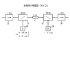
更に、本発明にしたがう多波長一括光増幅器は、図1に示す原理構成のエルビウムドープファイバを用い、図4の原理図に示されるように、エルビウムドープファイバに供給される複数種(図4では2種)の波長帯の励起光の光パワーを独立して制御可能に構成される。
【0025】
即ち、図4において、1は図1に示すエルビウムドープファイバ、21、26はアイソレータ、22、24は波長多重化部、23は0.98μmまたは0.51μmの励起光の発生部、25は1.48μmの励起光の発生部である。
【0026】
第一の波長多重化部22で0.98μmあるいは0.5μmの励起光を前方向にエルビウムドープファイバ1に送り、第二の波長多重化部24で1.48μmの励起光を後方向にエルビウムドープファイバ1に送りドープされたエルビウムを励起する。
【0027】
更に後に実施例において説明するようにエルビウムドープファイバ1において波長帯によりモードフィールド径が異なる。例えば0.98μm帯波長あるいは0.5μm帯波長は、1.48μm帯波長と比較して小さいため、0.98μmあるいは0.5μmは中心部のエルビウムドープ層(ガラス材Iの層)を選択的に励起可能である。これに対し、1.48μm帯波長は、外周のリング部のエルビウムドープ層(ガラス材IIの層)を選択的に励起可能である。
【0028】
これにより、中心部とリング部で励起率を独立に制御することができより広範囲の利得制御が可能となる。
【0029】
【実施例】
実施例1
図5に本発明の第一の実施例としてのエルビウムドープファイバ1の光導波部分10の断面構造を示す。図5において、破線円40内が図1に示す光導波部分10である。図5において、本実施例では、中心部領域41にGeO2 −SiO2 のガラス材層が配置されている。42はリング状に配置されるAl2 O3 −SiO2 のガラス材層である。
【0030】
これらガラス材層41及び42にはエルビウムがドープされている。光導波部分10の他の部分はシリカガラスで構成され、中心部のコア部を生成する領域には、不純物としてGeがドープされている。
【0031】
尚、上記のように、GeO2 −SiO2 を中心部のガラス材層41とし、Al2 O3 −SiO2 を、リング部のガラス材層42としているのは、次の理由に基づく。
【0032】
図5に示されるように、屈折率分布の0.98μm帯励起光のモードフィールド43は、1.48μm帯励起光のモードフィールド44より狭い。したがって、0.98μm帯励起光は中心部のエルビウムドープのガラス材層41対して、選択的に励起が可能であり、1.48μm帯励起光は、リング状のエルビウムドープのガラス材層42に対して選択的に励起が可能である。
【0033】
したがって、図5のエルビウムドープファイバを利用して構成される光増幅器は、図4の原理構成図において、エルビウムドープファイバ1を図5に示す構成とし、更に励起光発生器23から0.98μm帯励起光を前方向に供給し、励起光発生器25から1.48μm帯励起光を後方向に供給することにより、それぞれの励起光パワをガラス材層41及び42に対して、独立して制御が可能である。
【0034】
図6は、上記図5の実施例の効果を説明する図である。図6は横軸に信号光入力、縦軸に光出力とし、2つの波長帯励起光による利得差が無い(ΔG=0)時の最小利得と最大利得の関係を示すグラフである。
【0035】
図6において、(I)は導波部の中心部のみエルビウムをドープした一種類ののガラス材層からなる従来のエルビウムドープファイバを用いた光増幅器の特性である。この特性(I)は、−9〜−6dBmの信号光入力に対し、利得制御幅は、先に図10において説明したように約1dBmである。
【0036】
これに対し、本発明の図5にエルビウムドープファイバ1を用い、図4のように構成された光増幅器では、−12〜−6dBmの信号光入力に対し、4〜7.5dBm(平均約5.8dBm)の利得制御幅を得ることが出来る。
【0037】
実施例2
図5において、中心部のエルビウムをドープしたガラス材料層41をGeO2 −SiO2 からAl2 O2 −GeO2 −SiO2 に変え、1.55μm付近での利得をより広帯域とした例である。尚、光増幅器としての全体構成は実施例1と同様である。広帯域となるのは、図3において、図3(A)、図3(B)との比較によりGeO2 −SiO2 の例に対し、Al2 O2 −GeO2 −SiO2 の方が、吸収/放射断面積の帯域が広がっているためである。
【0038】
実施例3
図7は、本発明の一実施例として、本発明にしたがう実施例1のエルビウムドープファイバを用いた光増幅器50に、Al2 O3 −GeO2 −SiO2 ガラスにエルビウムをドープしたエルビウムドープファイバを用いた従来の光増幅器51を縦続したものである。
【0039】
かかる実施例では、エルビウムドープのGeO2 −SiO2 ガラス、エルビウムドープのGeO2 −Al2 O3 −SiO2 ガラス及びエルビウムドープのAl−Siガラスの3つのエルビウムドープ層の吸収/放射断面積をすべて利得制御に使うようにすることが出来る。
【0040】
実施例4
また、図示省略するが、上記図5に示す例と同様にして実施例2の光増幅器とGe−Siガラスにエルビウムをドープしたエルビウムドープファイバを用いた光増幅器を縦続して構成することが可能である。この場合にも、エルビウムドープGe−Siガラス、エルビウムドープGeO2 −SiO2 ガラス及びエルビウムドープAl2 O2 −GeO2 −SiO2 ガラスの吸収/放射断面積を使うようにすることが出来る。
【0041】
実施例5
図8、図9は、0.5μm、0.98μm、1.48μm帯励起光の3つのモードフィールドの差を利用し、それぞれのモードフィールドの差が大きいところで、ガラス材料を変えてエルビウムをドープしたファイバを適用する光増幅器の実施例である。
【0042】
即ち、図8にオイテ、光導波部10の断面図の60〜62は、それぞれ異なるガラス材料にエルビウムがドープされた領域である。更に、63〜65は、それぞれ0.5μm、0.98μm、1.48μm帯の屈折率分布のモードフィールドである。
【0043】
図9は図8のエルビウムドープファイバを利用する光増幅器の構成であり、他の実施例構成と異なる点は、カプラ26と励起光発生器27、28を有し、励起光発生器27、28からのそれぞれ0.5μm帯波長及び0.98μm帯波長のの励起光を混合し、波長分割変調器22を通して前方向に、エルビウムドープファイバ1に対して供給する構成である。
【0044】
尚、0.5μm帯波長の励起光を発生する励起光発生器28は、レーザダイオード単体による構成とせずに、倍波共振レーザSHG(1.064μmのYAGレーザ出力を倍波長にする装置)により構成することも可能である。
【0045】
尚、かかる実施例2〜5の場合も、図示は省略するが実施例1における図6に示した従来装置との比較における利得制御幅が大きくなると言う本発明の効果は同様である。
【0046】
【発明の効果】
以上、図に従い本発明の実施例を説明したように、従来の方法では利得制御範囲として1dB程度でしかなかったが、本発明の適用により大きな範囲の利得制御が可能である。
【0047】
また、上記実施例では、異なるエルビウムがドープされたガラス材料を二種以上使用することにより利得を一定に制御することを説明した。しかし、本発明はこれに限られない。即ち、本発明者によりエルビウムのドープ濃度に比例して励起光の吸収及び放射断面積が大きくなることが実験により確かめられている。
【0048】
したがって、ガラス材料を変える代わりにエルビウムのドープ量を変えることによっても同様に利得制御の範囲を大きくすることが可能である。
【図面の簡単な説明】
【図1】本発明の原理を説明するエルビウムドープファイバの断面構成例である。
【図2】励起率の変化による利得の依存性変化を説明する図である。
【図3】ガラス材料による励起光の吸収・放射特性の相違を説明する図である。
【図4】本発明の原理を説明するエルビウムドープファイバを用いた光増幅器の構成例である。
【図5】第1の実施例における光導波部分の断面構造を示す図である。
【図6】本発明の効果を説明する図である。
【図7】本発明の第3の実施例の構成図である。
【図8】本発明の第5の実施例におけるエルビウムドープファイバの光導波部分の断面構成を示す図である。
【図9】図8のエルビウムドープファイバを用いた光増幅器の構成例である。
【図10】0.98μmと1.48μmの2波長励起におけるそれぞれの励起光パワと総出力の関係である。
【符号の説明】
1 エルビウムドープファイバ
10 光導波部
21、26 アイソレータ
22、24 波長多重変調器
23、25 励起光発生部[0001]
TECHNICAL FIELD OF THE INVENTION
The present invention relates to an optical amplifier using an optical fiber doped with erbium (Er), and more particularly to a multi-wavelength collective optical amplifier that collectively amplifies a plurality of wavelength signals.
[0002]
[Prior art]
An optical amplifier using an optical fiber doped with erbium (Er) has been adopted for optical communication, and in recent years, in order to cope with an increase in the capacity of an optical communication system, development of collectively amplifying signals of a plurality of wavelengths has been advanced. . By collectively amplifying such signals of a plurality of wavelengths, it is possible to use only a single optical amplifier using an erbium-doped fiber, which has a great economic advantage.
[0003]
However, as a problem with such a multi-wavelength collective optical amplifier, there is gain controllability of each signal light output. As a gain control method, the present inventors have previously proposed a method of two-wavelength pumping of 0.98 μm and 1.48 μm (for example, a paper in the IEICE Preprints, “0.98 μm and 1.48 μm band wavelengths”). Multi-Wavelength Amplification Characteristics of EDFA by Excitation ”, issued March 10, 1995).
[0004]
FIG. 3 of this paper shows the relationship between the respective excitation light powers and the total output in two-wavelength excitation of 0.98 μm and 1.48 μm measured by the present inventors. FIG. 10 is an enlarged view of FIG. 10. In FIG. 10, the horizontal axis represents 0.98 μm band pumping light power, and the vertical axis represents 1.48 μm band pumping light power, and the total output as the sum of two signal light outputs. Is plotted.
[0005]
In the figure, when the power of the pumping light in the 0.98 μm band is 12.5 mW and the power of the pumping light in the 1.48 μm band is 22.5 mW, a total output of 11 dBm is obtained. FIG. 10 is a graph in which such a relationship is measured and plotted.
[0006]
On the other hand, in the multi-wavelength batch amplifier, it is desirable that the gain is constant for each wavelength, that is, there is no gain difference between a plurality of wavelengths. In FIG. 10, ΔG = 0 is a characteristic line obtained by plotting a point where there is no gain difference between two wavelengths of 0.98 μm and 1.48 μm.
[0007]
Therefore, in FIG. 10, the optical output can be controlled in the range of about 1 dBm from 12.5 dBm to 13.7 dBm by changing the 0.98 μm band pumping light power from 22 mW to 50 mW on the line of gain difference ΔG = 0. Can be read.
[0008]
[Problems to be solved by the invention]
However, in recent years, it has been desired to provide a system capable of further expanding the gain control range, for example, gain control over a range of about 6 dBm.
[0009]
In order to meet such a demand, the method proposed by the present inventors is not always sufficient. SUMMARY OF THE INVENTION Accordingly, an object of the present invention is to provide an optical amplifier that collectively amplifies a multi-wavelength signal that enables gain control in a larger range of 1 dBm or more.
[0010]
[Means for Solving the Problems]
The optical amplifier that solves the problem of the present invention is an optical amplifier that amplifies optical signals of a plurality of wavelengths collectively using an erbium-doped fiber as a basic configuration, and the erbium-doped fiber has a cross section in the cross-sectional direction. The erbium-doped glass material is composed of a plurality of types, and simultaneously has a plurality of types of excitation wavelength bands.
[0011]
Alternatively, the erbium-doped fiber has a plurality of doped regions having different wavelength characteristics of erbium absorption and emission in the cross-sectional direction, and at the same time, a plurality of types of excitation wavelength bands.
[0012]
Such a configuration is based on the inventor's recognition that, in the conventional example, the glass material doped with erbium is uniform, and the range of gain control cannot be made large. At least two types of materials, or a plurality of doped regions having different concentrations of erbium, and a plurality of types of excitation wavelength bands are also provided, thereby enabling a large control range. It is.
[0013]
That is, as a glass material doped with erbium, a plurality of types or a plurality of doped regions are provided, and by changing the doping concentrations thereof, the glass material is prevented from being uniform and the range of gain control is increased. are doing.
[0014]
BEST MODE FOR CARRYING OUT THE INVENTION
Hereinafter, embodiments of the present invention will be described with reference to the drawings. In the drawings, the same and similar components will be described with the same reference numerals and symbols. Here, in describing the embodiments of the present invention, first, the principle of the present invention will be described while examining the characteristics of a conventional optical amplifier.
[0015]
The wavelength characteristic of the gain of the optical amplifier is macroscopically determined by the pumping rate of the erbium-doped fiber as shown in FIG. Here, the excitation rate is defined as follows.
[0016]
That is, when the doped erbium shifts from the energy order N1 to the higher energy order N2 with respect to the injection of the excitation light, the excitation light is absorbed. On the other hand, when erbium electrons in the energy rank N2 fall to the energy rank N1 due to the excitation light, light is emitted. Therefore, the ratio of the energy rank N1 and the sum of the quantities in the energy rank N2 to the quantity N2 in the energy rank N2 (N1 + N2) is called the excitation rate.
[0017]
Therefore, it is known that if the excitation rate of the erbium-doped fiber is constant, the gain is determined correspondingly to this as shown in FIG.
[0018]
On the other hand, the present inventor has shown that the glass material of the erbium-doped fiber makes the absorption and emission cross-sectional area characteristics (the ratio of the absorption and emission of the excitation light: (Corresponding to the absorption and emission cross-sections), which resulted in a different wavelength dependence of gain for the same excitation rate.
[0019]
3A to 3C show absorption and emission cross-sectional area characteristics of Ge02-SiO2 glass, Al2O3-Ge02-SiO2 glass, and Al2O3-SiO2 glass, respectively.
[0020]
FIG. 1 is a principle configuration diagram of an optical amplifier for amplifying a plurality of wavelength optical signals of the present invention collectively based on the above recognition by the present inventors.
[0021]
In FIG. 1, (1) is a view showing a cross section of the erbium-doped
[0022]
FIG. 1 (2) is an enlarged view of the
[0023]
The glass material I and the glass material II are formed of different materials. That is, a glass material doped with erbium having different excitation light absorption / emission characteristics as described with reference to FIG. 3 is selected.
[0024]
Further, the multi-wavelength collective optical amplifier according to the present invention uses an erbium-doped fiber having the principle configuration shown in FIG. 1, and as shown in the principle diagram of FIG. 4, a plurality of types supplied to the erbium-doped fiber (FIG. The optical power of the excitation light in the two types of wavelength bands can be controlled independently.
[0025]
That is, in FIG. 4, 1 is the erbium-doped fiber shown in FIG. 1, 21 and 26 are isolators, 22 and 24 are wavelength multiplexing units, 23 is a 0.98 μm or 0.51 μm excitation light generating unit, and 25 is 1 .48 μm excitation light generation section.
[0026]
The first wavelength multiplexing unit 22 sends the pump light of 0.98 μm or 0.5 μm forward to the erbium-doped
[0027]
Further, as described later in the embodiments, the mode field diameter of the erbium-doped
[0028]
As a result, the excitation rate can be independently controlled in the center portion and the ring portion, and gain control over a wider range is possible.
[0029]
【Example】
Example 1
FIG. 5 shows a cross-sectional structure of an
[0030]
These glass material layers 41 and 42 are doped with erbium. The other portion of the
[0031]
As described above, the reason why GeO 2 —SiO 2 is used as the
[0032]
As shown in FIG. 5, the
[0033]
Therefore, the optical amplifier using the erbium-doped fiber of FIG. 5 has the configuration shown in FIG. 4 in which the erbium-doped
[0034]
FIG. 6 is a diagram for explaining the effect of the embodiment of FIG. FIG. 6 is a graph showing the relationship between the minimum gain and the maximum gain when there is no gain difference between two wavelength band pump lights (ΔG = 0), with the signal light input on the horizontal axis and the optical output on the vertical axis.
[0035]
In FIG. 6, (I) shows the characteristics of an optical amplifier using a conventional erbium-doped fiber composed of one type of glass material layer doped with erbium only at the center of the waveguide. In the characteristic (I), the gain control width is about 1 dBm for the signal light input of -9 to -6 dBm as described above with reference to FIG.
[0036]
On the other hand, in the optical amplifier configured as shown in FIG. 4 using the erbium-doped
[0037]
Example 2
FIG. 5 shows an example in which the
[0038]
Example 3
FIG. 7 shows an erbium-doped fiber in which Al 2 O 3 -GeO 2 -SiO 2 glass is doped with erbium in an
[0039]
In such embodiments, GeO 2 -SiO 2 glass of the erbium-doped, the absorption / emission cross section of GeO 2 -Al 2 O 3 -
[0040]
Example 4
Although not shown, it is possible to cascade the optical amplifier of the second embodiment and an optical amplifier using an erbium-doped fiber in which Ge-Si glass is doped with erbium in the same manner as in the example shown in FIG. It is. Also in this case, an erbium-doped Ge-Si glass, erbium doped GeO 2 -SiO 2 glass and erbium-doped Al 2 O 2 -GeO 2 -
[0041]
Example 5
FIGS. 8 and 9 use the difference between the three mode fields of the 0.5 μm, 0.98 μm, and 1.48 μm band excitation light, and change the glass material to dope erbium where the difference between the respective mode fields is large. 1 is an embodiment of an optical amplifier to which a modified fiber is applied.
[0042]
That is, 60 to 62 in the cross-sectional view of the
[0043]
FIG. 9 shows a configuration of an optical amplifier using the erbium-doped fiber of FIG. 8, which is different from the configuration of the other embodiment in that it has a coupler 26 and pumping
[0044]
The pumping
[0045]
In the case of the second to fifth embodiments as well, although not shown, the effect of the present invention that the gain control width in the first embodiment is larger than that of the conventional device shown in FIG. 6 is the same.
[0046]
【The invention's effect】
As described above, the gain control range of the conventional method is only about 1 dB as described in the embodiment of the present invention with reference to the drawings. However, by applying the present invention, a large range of gain control is possible.
[0047]
Further, in the above-described embodiment, it has been described that the gain is controlled to be constant by using two or more kinds of glass materials doped with different erbium. However, the present invention is not limited to this. That is, the present inventor has confirmed by experiment that the absorption and emission cross sections of the excitation light increase in proportion to the erbium doping concentration.
[0048]
Accordingly, the range of gain control can be similarly increased by changing the erbium doping amount instead of changing the glass material.
[Brief description of the drawings]
FIG. 1 is a cross-sectional configuration example of an erbium-doped fiber for explaining the principle of the present invention.
FIG. 2 is a diagram for explaining a change in gain dependency due to a change in excitation rate.
FIG. 3 is a diagram illustrating a difference in absorption / emission characteristics of excitation light between glass materials.
FIG. 4 is a configuration example of an optical amplifier using an erbium-doped fiber for explaining the principle of the present invention.
FIG. 5 is a diagram showing a cross-sectional structure of an optical waveguide portion in the first embodiment.
FIG. 6 is a diagram illustrating the effect of the present invention.
FIG. 7 is a configuration diagram of a third embodiment of the present invention.
FIG. 8 is a diagram showing a cross-sectional configuration of an optical waveguide portion of an erbium-doped fiber according to a fifth embodiment of the present invention.
9 is a configuration example of an optical amplifier using the erbium-doped fiber of FIG.
FIG. 10 shows the relationship between the respective pumping light powers and the total output in two-wavelength pumping at 0.98 μm and 1.48 μm.
[Explanation of symbols]
DESCRIPTION OF
Claims (5)
前記エルビウムドープファイバの光導波部を、エルビウムとゲルマニウムがドープされた中心部を成す第1のガラス材料層と、前記第1のガラス材料層の外側にエルビウムとアルミニウムがドープされた第2のガラス材料層で形成し、
それぞれ0.98μm、1.48μmの励起波長帯の第1、第2の励起光を出力する励起光源を有し、
前記励起光源より出力される第1、第2の励起光を、それぞれ独立に励起光パワーを制御可能に、前記エルビウムドープファイバに供給する ように構成されたことを特徴とする光増幅器。An optical amplifier that collectively amplifies optical signals of a plurality of wavelengths using an erbium-doped fiber,
The optical waveguide portion of the erbium-doped fiber is formed by a first glass material layer forming a central portion doped with erbium and germanium, and a second glass doped with erbium and aluminum outside the first glass material layer. Formed with a material layer,
An excitation light source that outputs first and second excitation lights in an excitation wavelength band of 0.98 μm and 1.48 μm, respectively;
An optical amplifier, wherein the first and second pumping lights output from the pumping light source are supplied to the erbium-doped fiber such that the pumping light power can be controlled independently of each other .
前記ゲルマニウムがドープされた中心部を成す第1のガラス材料層をGeO2−SiO2ガラスとし、前記アルミニウムがドープされた第2のガラス材料層をAl2O3−SiO2ガラスとしたことを特徴とする光増幅器。The optical amplifier according to claim 1 ,
The first glass material layer forming the central portion doped with germanium is made of GeO 2 —SiO 2 glass, and the second glass material layer doped with aluminum is made of Al 2 O 3 —SiO 2 glass. Characteristic optical amplifier.
前記ゲルマニウムがドープされた中心部を成す第1のガラス材料層をGeO2−Al2O3−SiO2ガラスとし、前記アルミニウムがドープされた第2のガラス材料層をAl2O3−SiO2ガラスとしたことを特徴とする光増幅器。The optical amplifier according to claim 1 ,
The first glass material layer forming the central portion doped with germanium is GeO 2 —Al 2 O 3 —SiO 2 glass, and the second glass material layer doped with aluminum is Al 2 O 3 —SiO 2 An optical amplifier characterized by being made of glass.
前記第1の光増幅器は、前記エルビウムドープファイバの光導波部が、エルビウムとゲルマニウムがドープされた中心部を成す第1のガラス材料層と、前記第1のガラス材料層の外側にエルビウムとアルミニウムがドープされた第2のガラス材料層で形成し、それぞれ0.98μm、1.48μmの励起波長帯の第1、第2の励起光を出力する励起光源を有し、前記励起光源より出力される第1、第2の励起光を、それぞれ独立に励起光パワーを制御可能に、前記エルビウムドープファイバに供給するように構成し、前記ゲルマニウムがドープされた中心部を 成す第1のガラス材料層をGeO 2 −SiO 2 ガラスとし、前記アルミニウムがドープされた第2のガラス材料層をAl 2 O 3 −SiO 2 ガラスとする光増幅器であって、
前記第2の光増幅器は、Al2O3−GeO2−SiO2ガラスのエルビウムドープファイバによる光増幅器である
ことを特徴とする光増幅器。 A first optical amplifier and a second optical amplifier, each having an erbium-doped fiber, connected in tandem;
In the first optical amplifier, the optical waveguide portion of the erbium-doped fiber may include a first glass material layer forming a central portion doped with erbium and germanium, and erbium and aluminum outside the first glass material layer. And a pumping light source that outputs first and second pumping light in a pumping wavelength band of 0.98 μm and 1.48 μm, respectively. A first glass material layer forming a central portion doped with germanium, wherein the first and second pump lights are supplied to the erbium-doped fiber so that the pump light power can be controlled independently of each other. Is a GeO 2 —SiO 2 glass, and the aluminum-doped second glass material layer is an Al 2 O 3 —SiO 2 glass,
It said second optical amplifier, Al 2 O 3 -GeO 2 -SiO 2 glass of the erbium-doped fiber optical amplifier according to claim <br/> is an optical amplifier according to.
前記第1の光増幅器は、前記エルビウムドープファイバの光導波部が、エルビウムとゲルマニウムがドープされた中心部を成す第1のガラス材料層と、前記第1のガラス材料層の外側にエルビウムとアルミニウムがドープされた第2のガラス材料層で形成され、それぞれ0.98μm、1.48μmの励起波長帯の第1、第2の励起光を出力する第1、第2の励起光源を有し、前記第1、第2の励起光源より出力される第1、第2の励起光を、それぞれ独立に励起光パワーを制御可能に、前記エルビウムドープファイバに供給するように構成され、前記ゲルマニウムがドープされた中心部を成す第1のガラス材料層をGeO 2 −Al 2 O 3 −SiO 2 ガラスとし、前記アルミニウムがドープされた第2のガラス材料層をAl 2 O 3 −SiO 2 ガラスとする光増幅器であって、
前記第2の光増幅器は、GeO2−SiO2ガラスのエルビウムドープファイバによる光増幅器である
ことを特徴とする光増幅器。 A first optical amplifier and a second optical amplifier, each having an erbium-doped fiber, connected in tandem;
In the first optical amplifier, the optical waveguide portion of the erbium-doped fiber may include a first glass material layer forming a central portion doped with erbium and germanium, and erbium and aluminum outside the first glass material layer. Is formed of a second glass material layer doped with, and has first and second excitation light sources that output first and second excitation light in an excitation wavelength band of 0.98 μm and 1.48 μm, respectively. The first and second pump lights output from the first and second pump light sources are supplied to the erbium-doped fiber so that the pump light power can be controlled independently, and the germanium is doped. has been the first glass material layer forming the center portion and GeO 2 -Al 2 O 3 -SiO 2 glass, the second glass material layer in which the aluminum-doped Al 2 O 3 -S An optical amplifier as O 2 glass,
Said second optical amplifier, an optical amplifier according to claim <br/> is an optical amplifier according to GeO 2 -SiO 2 erbium-doped fiber glass.
Priority Applications (5)
| Application Number | Priority Date | Filing Date | Title |
|---|---|---|---|
| JP28118295A JP3556026B2 (en) | 1995-10-30 | 1995-10-30 | Multi-wavelength optical amplifier that amplifies multiple wavelength signals at once |
| GB9622278A GB2306763B (en) | 1995-10-30 | 1996-10-25 | Optical amplifier for wavelength division multiplexed signals |
| US08/736,733 US5861973A (en) | 1995-10-30 | 1996-10-25 | Optical amplifier for collectively amplifying optical signals having a plurality of multiplexed wavelengths |
| FR9613236A FR2740620B1 (en) | 1995-10-30 | 1996-10-30 | OPTICAL AMPLIFIER, AND ASSEMBLY COMPRISING SAME |
| GBGB9923183.9A GB9923183D0 (en) | 1995-10-30 | 1999-09-30 | Optical amplifier for wavelength division multiplexed signals |
Applications Claiming Priority (1)
| Application Number | Priority Date | Filing Date | Title |
|---|---|---|---|
| JP28118295A JP3556026B2 (en) | 1995-10-30 | 1995-10-30 | Multi-wavelength optical amplifier that amplifies multiple wavelength signals at once |
Publications (2)
| Publication Number | Publication Date |
|---|---|
| JPH09129948A JPH09129948A (en) | 1997-05-16 |
| JP3556026B2 true JP3556026B2 (en) | 2004-08-18 |
Family
ID=17635493
Family Applications (1)
| Application Number | Title | Priority Date | Filing Date |
|---|---|---|---|
| JP28118295A Expired - Fee Related JP3556026B2 (en) | 1995-10-30 | 1995-10-30 | Multi-wavelength optical amplifier that amplifies multiple wavelength signals at once |
Country Status (4)
| Country | Link |
|---|---|
| US (1) | US5861973A (en) |
| JP (1) | JP3556026B2 (en) |
| FR (1) | FR2740620B1 (en) |
| GB (2) | GB2306763B (en) |
Families Citing this family (22)
| Publication number | Priority date | Publication date | Assignee | Title |
|---|---|---|---|---|
| GB2335074B (en) * | 1996-12-04 | 2002-02-13 | Univ Southampton | Optical Amplifier |
| US5926600A (en) * | 1997-05-22 | 1999-07-20 | Litton Systems, Inc. | Optical fiber for reducing optical signal reflections |
| JPH11121839A (en) * | 1997-10-17 | 1999-04-30 | Fujitsu Ltd | Optical amplification fiber and optical fiber amplifier |
| JP2000252559A (en) * | 1999-03-01 | 2000-09-14 | Nec Corp | Double clad fiber and optical fiber amplifier |
| KR100326119B1 (en) | 1999-06-23 | 2002-03-07 | 윤종용 | L-band optical fiber amplifier by use of seed beam |
| KR100334809B1 (en) | 1999-07-21 | 2002-05-02 | 윤종용 | Broad band light source by use of seed beam |
| KR100334789B1 (en) * | 1999-07-22 | 2002-05-02 | 윤종용 | Wide band light source for testing optic elements using feedback loop |
| JP4269453B2 (en) * | 1999-12-10 | 2009-05-27 | 住友電気工業株式会社 | Optical fiber for optical amplification and optical fiber amplifier |
| GB2363675B (en) | 2000-01-19 | 2004-05-26 | Advantest Corp | Wideband optical amplifier and wideband variable wavelength optical source |
| WO2001069734A1 (en) * | 2000-03-10 | 2001-09-20 | Corning Incorporated | Optical fiber with absorbing overclad glass layer |
| US6487006B1 (en) * | 2000-05-12 | 2002-11-26 | Jds Uniphase Inc. | Simultaneous single mode and multi-mode propagation of signals in a double clad optical fiber |
| US6377396B1 (en) | 2000-09-26 | 2002-04-23 | Onetta, Inc. | Optical amplifiers with variable optical attenuation for use in fiber-optic communications systems |
| US6417961B1 (en) | 2000-10-10 | 2002-07-09 | Onetta, Inc. | Optical amplifiers with dispersion compensation |
| US6687049B1 (en) | 2001-07-03 | 2004-02-03 | Onetta, Inc. | Optical amplifiers with stable output power under low input power conditions |
| ATE251352T1 (en) * | 2001-07-23 | 2003-10-15 | Cit Alcatel | OPTICAL FIBER AMPLIFIER AND COMMUNICATIONS SYSTEM USING THE SAME |
| US6577789B1 (en) | 2001-09-26 | 2003-06-10 | Onetta, Inc. | Double-pass optical amplifiers and optical network equipment |
| US20030099450A1 (en) * | 2001-11-28 | 2003-05-29 | Huailiang Wei | Profile for limited mode fiber |
| US7346258B2 (en) | 2002-07-09 | 2008-03-18 | Fujikura Ltd. | Optical fiber and optical fiber coupler, erbium-doped optical fiber amplifier, and optical waveguide using the same |
| EP1865582B1 (en) * | 2005-03-30 | 2017-09-06 | Fujitsu Limited | Optical fibre amplifier |
| JP5566568B2 (en) * | 2007-03-27 | 2014-08-06 | ピーエスフォー ルクスコ エスエイアールエル | Power supply voltage generation circuit |
| CN111129927A (en) * | 2019-12-30 | 2020-05-08 | 大族激光科技产业集团股份有限公司 | Fiber laser and laser emitting device |
| CN112142319B (en) * | 2020-11-26 | 2021-03-16 | 武汉光谷航天三江激光产业技术研究院有限公司 | Axial absorption gradient optical fiber, preparation method thereof and optical fiber laser |
Family Cites Families (15)
| Publication number | Priority date | Publication date | Assignee | Title |
|---|---|---|---|---|
| DE4002369A1 (en) * | 1990-01-27 | 1991-08-01 | Standard Elektrik Lorenz Ag | Multistage fibre=optic amplifier - provides constant amplification over large range of wavelengths using selective directional coupler and pump light source |
| JP2856501B2 (en) * | 1990-04-27 | 1999-02-10 | 株式会社東芝 | Optical fiber amplifier |
| US5155621A (en) * | 1990-07-31 | 1992-10-13 | Fujitsu Limited | Optical fiber amplifier |
| US5058976A (en) * | 1990-08-03 | 1991-10-22 | At&T Bell Laboratories | System comprising Er-doped optical fiber |
| US5140456A (en) * | 1991-04-08 | 1992-08-18 | General Instrument Corporation | Low noise high power optical fiber amplifier |
| FR2674965B1 (en) * | 1991-04-08 | 1993-12-31 | Alcatel Nv | OPTICAL AMPLIFIER WITH FIBER OPTIC DOPED WITH ERBIUM. |
| DK168180B1 (en) * | 1991-07-19 | 1994-02-21 | Lycom As | Method of amplifying an optical signal, optical amplifier for practicing the method, and using such an optical amplifier as a light source |
| DE4208858A1 (en) * | 1992-03-19 | 1993-09-23 | Sel Alcatel Ag | FIBER OPTICAL AMPLIFIER WITH CONTROL OF THE PUMP LIGHT WAVELENGTH |
| JP3259105B2 (en) * | 1992-08-19 | 2002-02-25 | 富士通株式会社 | Optical fiber amplifier |
| JPH06318754A (en) * | 1993-05-10 | 1994-11-15 | Matsushita Electric Ind Co Ltd | Optical fiber amplifier and light signal transmission system |
| JP2636152B2 (en) * | 1993-11-24 | 1997-07-30 | 住友電気工業株式会社 | Optical fiber amplifier and optical communication system |
| JP3244579B2 (en) * | 1993-12-17 | 2002-01-07 | 富士通株式会社 | Optical fiber amplifier |
| FR2715017B1 (en) * | 1994-01-13 | 1996-02-16 | Alcatel Nv | Transmission method and optical link with spectral multiplexing with amplification. |
| JP3379052B2 (en) * | 1994-09-26 | 2003-02-17 | 富士通株式会社 | WDM optical amplifier, WDM transmission system, and WDM transmission method |
| JP3301275B2 (en) * | 1994-09-27 | 2002-07-15 | 日本電信電話株式会社 | Optical fiber amplifier |
-
1995
- 1995-10-30 JP JP28118295A patent/JP3556026B2/en not_active Expired - Fee Related
-
1996
- 1996-10-25 US US08/736,733 patent/US5861973A/en not_active Expired - Fee Related
- 1996-10-25 GB GB9622278A patent/GB2306763B/en not_active Expired - Fee Related
- 1996-10-30 FR FR9613236A patent/FR2740620B1/en not_active Expired - Fee Related
-
1999
- 1999-09-30 GB GBGB9923183.9A patent/GB9923183D0/en not_active Ceased
Also Published As
| Publication number | Publication date |
|---|---|
| FR2740620B1 (en) | 1999-08-06 |
| GB9923183D0 (en) | 1999-12-01 |
| GB9622278D0 (en) | 1996-12-18 |
| GB2306763A (en) | 1997-05-07 |
| JPH09129948A (en) | 1997-05-16 |
| GB2306763B (en) | 1999-12-01 |
| FR2740620A1 (en) | 1997-04-30 |
| US5861973A (en) | 1999-01-19 |
Similar Documents
| Publication | Publication Date | Title |
|---|---|---|
| JP3556026B2 (en) | Multi-wavelength optical amplifier that amplifies multiple wavelength signals at once | |
| JP3247292B2 (en) | Optical communication system | |
| US6836607B2 (en) | Cladding-pumped 3-level fiber laser/amplifier | |
| JP3291578B2 (en) | Fiber amplifier | |
| US5287216A (en) | Fiber amplifier with multiple pumps | |
| US5497265A (en) | High-power signals optical generator for telecommunication systems | |
| US6353499B2 (en) | Optical fiber amplifier with oscillating pump energy | |
| CN101288211A (en) | Optical fibre laser | |
| JPH10190112A (en) | Optical amplifier | |
| KR100353974B1 (en) | Lasers, optical amplifiers, and amplification methods | |
| JPH11121839A (en) | Optical amplification fiber and optical fiber amplifier | |
| JP3621220B2 (en) | Optical amplifier and optical waveguide structure | |
| CA2173662C (en) | Rare earth element-doped optical fiber amplifier | |
| JPH0563259A (en) | Optical fiber amplifier | |
| JP4134511B2 (en) | Rare earth element doped optical fiber and optical device using the same | |
| US20080130100A1 (en) | High-efficiency, high-reliability fiber amplifier using engineered passband of photonic bandgap optical fiber | |
| JP2960674B2 (en) | Optical fiber for amplification | |
| US5638204A (en) | Optical power amplifier with Al2 O3 and erbium doped active fiber | |
| JP2693662B2 (en) | Optical amplifier | |
| JP2003031879A (en) | Optical device, optical fiber used therefor, pulse generator, optical amplifier, and fiber laser | |
| JPH10242548A (en) | Er added multicore fiber and light amplifier using the same | |
| JP4075113B2 (en) | Optical fiber amplifier and erbium-doped optical fiber | |
| CN210577001U (en) | Optical fiber laser | |
| US20030117699A1 (en) | Use of photonic band gap structures in optical amplifiers | |
| JPH09265021A (en) | Multifiber core, optical amplifier formed by using the same, optical amplifier repeater formed by using the optical amplifier and optical amplifier distributor |
Legal Events
| Date | Code | Title | Description |
|---|---|---|---|
| TRDD | Decision of grant or rejection written | ||
| A01 | Written decision to grant a patent or to grant a registration (utility model) |
Free format text: JAPANESE INTERMEDIATE CODE: A01 Effective date: 20040511 |
|
| A61 | First payment of annual fees (during grant procedure) |
Free format text: JAPANESE INTERMEDIATE CODE: A61 Effective date: 20040511 |
|
| R150 | Certificate of patent or registration of utility model |
Free format text: JAPANESE INTERMEDIATE CODE: R150 |
|
| LAPS | Cancellation because of no payment of annual fees |