JP3552623B2 - Composite material and heat sink for semiconductor device using the same - Google Patents
Composite material and heat sink for semiconductor device using the same Download PDFInfo
- Publication number
- JP3552623B2 JP3552623B2 JP37268399A JP37268399A JP3552623B2 JP 3552623 B2 JP3552623 B2 JP 3552623B2 JP 37268399 A JP37268399 A JP 37268399A JP 37268399 A JP37268399 A JP 37268399A JP 3552623 B2 JP3552623 B2 JP 3552623B2
- Authority
- JP
- Japan
- Prior art keywords
- composite material
- heat sink
- copper
- module
- thermal conductivity
- Prior art date
- Legal status (The legal status is an assumption and is not a legal conclusion. Google has not performed a legal analysis and makes no representation as to the accuracy of the status listed.)
- Expired - Fee Related
Links
Images


Classifications
-
- H—ELECTRICITY
- H01—ELECTRIC ELEMENTS
- H01L—SEMICONDUCTOR DEVICES NOT COVERED BY CLASS H10
- H01L2224/00—Indexing scheme for arrangements for connecting or disconnecting semiconductor or solid-state bodies and methods related thereto as covered by H01L24/00
- H01L2224/01—Means for bonding being attached to, or being formed on, the surface to be connected, e.g. chip-to-package, die-attach, "first-level" interconnects; Manufacturing methods related thereto
- H01L2224/42—Wire connectors; Manufacturing methods related thereto
- H01L2224/44—Structure, shape, material or disposition of the wire connectors prior to the connecting process
- H01L2224/45—Structure, shape, material or disposition of the wire connectors prior to the connecting process of an individual wire connector
- H01L2224/45001—Core members of the connector
- H01L2224/45099—Material
- H01L2224/451—Material with a principal constituent of the material being a metal or a metalloid, e.g. boron (B), silicon (Si), germanium (Ge), arsenic (As), antimony (Sb), tellurium (Te) and polonium (Po), and alloys thereof
- H01L2224/45117—Material with a principal constituent of the material being a metal or a metalloid, e.g. boron (B), silicon (Si), germanium (Ge), arsenic (As), antimony (Sb), tellurium (Te) and polonium (Po), and alloys thereof the principal constituent melting at a temperature of greater than or equal to 400°C and less than 950°C
- H01L2224/45124—Aluminium (Al) as principal constituent
-
- H—ELECTRICITY
- H01—ELECTRIC ELEMENTS
- H01L—SEMICONDUCTOR DEVICES NOT COVERED BY CLASS H10
- H01L2224/00—Indexing scheme for arrangements for connecting or disconnecting semiconductor or solid-state bodies and methods related thereto as covered by H01L24/00
- H01L2224/01—Means for bonding being attached to, or being formed on, the surface to be connected, e.g. chip-to-package, die-attach, "first-level" interconnects; Manufacturing methods related thereto
- H01L2224/42—Wire connectors; Manufacturing methods related thereto
- H01L2224/44—Structure, shape, material or disposition of the wire connectors prior to the connecting process
- H01L2224/45—Structure, shape, material or disposition of the wire connectors prior to the connecting process of an individual wire connector
- H01L2224/45001—Core members of the connector
- H01L2224/45099—Material
- H01L2224/451—Material with a principal constituent of the material being a metal or a metalloid, e.g. boron (B), silicon (Si), germanium (Ge), arsenic (As), antimony (Sb), tellurium (Te) and polonium (Po), and alloys thereof
- H01L2224/45138—Material with a principal constituent of the material being a metal or a metalloid, e.g. boron (B), silicon (Si), germanium (Ge), arsenic (As), antimony (Sb), tellurium (Te) and polonium (Po), and alloys thereof the principal constituent melting at a temperature of greater than or equal to 950°C and less than 1550°C
- H01L2224/45144—Gold (Au) as principal constituent
-
- H—ELECTRICITY
- H01—ELECTRIC ELEMENTS
- H01L—SEMICONDUCTOR DEVICES NOT COVERED BY CLASS H10
- H01L2224/00—Indexing scheme for arrangements for connecting or disconnecting semiconductor or solid-state bodies and methods related thereto as covered by H01L24/00
- H01L2224/01—Means for bonding being attached to, or being formed on, the surface to be connected, e.g. chip-to-package, die-attach, "first-level" interconnects; Manufacturing methods related thereto
- H01L2224/42—Wire connectors; Manufacturing methods related thereto
- H01L2224/47—Structure, shape, material or disposition of the wire connectors after the connecting process
- H01L2224/48—Structure, shape, material or disposition of the wire connectors after the connecting process of an individual wire connector
- H01L2224/484—Connecting portions
- H01L2224/4847—Connecting portions the connecting portion on the bonding area of the semiconductor or solid-state body being a wedge bond
- H01L2224/48472—Connecting portions the connecting portion on the bonding area of the semiconductor or solid-state body being a wedge bond the other connecting portion not on the bonding area also being a wedge bond, i.e. wedge-to-wedge
-
- H—ELECTRICITY
- H01—ELECTRIC ELEMENTS
- H01L—SEMICONDUCTOR DEVICES NOT COVERED BY CLASS H10
- H01L2224/00—Indexing scheme for arrangements for connecting or disconnecting semiconductor or solid-state bodies and methods related thereto as covered by H01L24/00
- H01L2224/01—Means for bonding being attached to, or being formed on, the surface to be connected, e.g. chip-to-package, die-attach, "first-level" interconnects; Manufacturing methods related thereto
- H01L2224/42—Wire connectors; Manufacturing methods related thereto
- H01L2224/47—Structure, shape, material or disposition of the wire connectors after the connecting process
- H01L2224/49—Structure, shape, material or disposition of the wire connectors after the connecting process of a plurality of wire connectors
- H01L2224/491—Disposition
- H01L2224/49105—Connecting at different heights
- H01L2224/49109—Connecting at different heights outside the semiconductor or solid-state body
-
- H—ELECTRICITY
- H01—ELECTRIC ELEMENTS
- H01L—SEMICONDUCTOR DEVICES NOT COVERED BY CLASS H10
- H01L2924/00—Indexing scheme for arrangements or methods for connecting or disconnecting semiconductor or solid-state bodies as covered by H01L24/00
- H01L2924/013—Alloys
- H01L2924/0132—Binary Alloys
- H01L2924/01322—Eutectic Alloys, i.e. obtained by a liquid transforming into two solid phases
-
- H—ELECTRICITY
- H01—ELECTRIC ELEMENTS
- H01L—SEMICONDUCTOR DEVICES NOT COVERED BY CLASS H10
- H01L2924/00—Indexing scheme for arrangements or methods for connecting or disconnecting semiconductor or solid-state bodies as covered by H01L24/00
- H01L2924/10—Details of semiconductor or other solid state devices to be connected
- H01L2924/11—Device type
- H01L2924/13—Discrete devices, e.g. 3 terminal devices
- H01L2924/1301—Thyristor
-
- H—ELECTRICITY
- H01—ELECTRIC ELEMENTS
- H01L—SEMICONDUCTOR DEVICES NOT COVERED BY CLASS H10
- H01L2924/00—Indexing scheme for arrangements or methods for connecting or disconnecting semiconductor or solid-state bodies as covered by H01L24/00
- H01L2924/10—Details of semiconductor or other solid state devices to be connected
- H01L2924/11—Device type
- H01L2924/13—Discrete devices, e.g. 3 terminal devices
- H01L2924/1304—Transistor
- H01L2924/1305—Bipolar Junction Transistor [BJT]
- H01L2924/13055—Insulated gate bipolar transistor [IGBT]
-
- H—ELECTRICITY
- H01—ELECTRIC ELEMENTS
- H01L—SEMICONDUCTOR DEVICES NOT COVERED BY CLASS H10
- H01L2924/00—Indexing scheme for arrangements or methods for connecting or disconnecting semiconductor or solid-state bodies as covered by H01L24/00
- H01L2924/10—Details of semiconductor or other solid state devices to be connected
- H01L2924/11—Device type
- H01L2924/13—Discrete devices, e.g. 3 terminal devices
- H01L2924/1304—Transistor
- H01L2924/1306—Field-effect transistor [FET]
- H01L2924/13091—Metal-Oxide-Semiconductor Field-Effect Transistor [MOSFET]
Landscapes
- Cooling Or The Like Of Semiconductors Or Solid State Devices (AREA)
- Manufacture Of Alloys Or Alloy Compounds (AREA)
Description
【0001】
【発明の属する技術分野】
本発明は、低熱膨張性と高熱伝導性を有する銅複合材料及びそれを用いた放熱板と半導体装置に関する。
【0002】
【従来の技術】
電子デバイスによる電力やエネルギーの変換,制御に関連した技術、特にオン,オフモードで用いられる電力用電子デバイスとその応用技術としての電力変換システムがパワーエレクトロニクスである。
【0003】
電力変換のため、各種のオン,オフ機能を持つ電力用半導体素子が用いられている。この半導体素子としては、pn接合体を内蔵し、一方向のみの導電性をもつ整流ダイオードをはじめ、種々のpn接合の組合せ構造により、サイリスタ,バイボーラトランジスタ,MOSFET等が実用化され、更には絶縁ゲート型バイポーラトランジスタ(IGBT)やゲート信号によりターンオフ機能を併せもつゲートターンオフサイリスタ(GTO)も開発されている。
【0004】
これらの電力用半導体素子は、通電により発熱し、その高容量化,高速化に伴い発熱量も増大する傾向にある。発熱に起因する半導体素子の特性劣化,短寿命化を防止するためには、放熱部を設け、半導体素子及びその近傍での温度上昇を抑制する必要がある。銅は、熱伝導率が393W/m・kと大きく、かつ低価格であるため、放熱部材として一般に用いられている。しかし、電力用半導体素子を備える半導体装置の放熱部材は、熱膨張率が4.2×10−6/℃ のSiと接合されるため、熱膨張率がこれに近い放熱部材が望まれる。銅は熱膨張率が17×10−6/℃と大きいため、半導体素子との半田接合性は好ましくなく、MoやWといった熱膨張率がSiと近い材料を放熱部材として用いたり、半導体素子と放熱部材の間に設けたりしている。
【0005】
一方、電子回路を一つの半導体チップ上に集積させた集積回路(IC)は、その機能に応じてメモリー,ロジック,マイクロプロセッサ等に分類される。これらは電力用半導体素子に対し、電子用半導体素子と呼ばれる。これらの半導体素子の集積度や演算速度は年々増加し、それに伴い発熱量も増大している。ところで、一般に電子用半導体素子は、外気から遮断して故障や劣化を防止する目的で、パッケージ内に収納されている。この多くは、半導体素子がセラミックスにダイボンディングされ、密封されているセラミックスパッケージ及び樹脂で封止されているプラスチックパッケージである。また、高信頼性,高速化に対応するために、複数個の半導体装置を一つの基板上に搭載したマルチチップモジュール (MCM)も製造されている。
【0006】
プラスチックパッケージは、リードフレームと半導体素子の端子がボンディングワイヤにより接続され、これを樹脂で封止する構造になっている。近年は、半導体素子の発熱量の増大に伴い、リードフレームに熱放散性を持たせたパッケージや熱放散のための放熱板を搭載するパッケージも出現している。熱放散のためには、熱伝導率の大きい銅系のリードフレームや放熱板が多用されているが、
Siとの熱膨張差による不具合が懸念されている。
【0007】
一方、セラミックスパッケージは、配線がプリントされたセラミック基板上に半導体素子が搭載され、金属やセラミックスのキャップで密封する構造を持つ。さらに、セラミック基板にはCu−MoやCu−Wの複合材料あるいはコバール合金などが接合され、放熱板としてして用いられているが、それぞれの材料において低熱膨張化あるいは高熱伝導化とともに加工性の向上,低コストが要求されている。
【0008】
MCMはSi,金属、あるいはセラミックスの基板上に形成された薄膜配線に複数個の半導体素子をベアチップで搭載し、これをセラミックスパッケージに入れ、リッドで封止する構造を持つ。放熱性が要求される場合には、パッケージに放熱板や放熱フィンを設置する。金属製の基板材料として、銅やアルミニウムが使用されており、これらは熱伝導度が高いという長所を持つが、熱膨張係数が大きく半導体素子との整合性が悪い。このため、低信頼性MCMの基板にはSiや窒化アルミニウム(AlN)が用いられている。また、放熱板はセラミックスパッケージと接合されるため、熱膨張率の点でパッケージ材料と整合性が良く、熱伝導率が大きな材料が望まれている。
【0009】
【発明が解決しようとする課題】
以上のように、半導体素子を搭載した半導体装置は、いずれもその動作において熱を発生し、蓄熱されると半導体素子の機能を損ねる恐れがある。このため、発生する熱を外部に放散するための熱伝導性に優れた放熱板が必要となる。放熱板は、直接あるいは絶縁層を介して半導体素子と接合されるため、熱伝導性だけでなく、熱膨張の点でも半導体素子との整合性が要求される。
【0010】
現在用いられている半導体素子は、主にSi及びGaAsである。これらの熱膨張係数は、それぞれ2.6×10⁻⁶〜3.6×10⁻⁶/℃,5.7×10−6〜6.9×10−6/℃である。これらに近い熱膨張係数をもつ放熱板材料には、従来よりAlN,SiC,Mo,W,Cu−W等が知られているが、これらは単一材料であるため、熱伝達係数と熱伝導率を任意にコントロールする事は困難であるとともに、加工性に乏しくコストが高いという問題がある。
【0011】
最近になって、放熱板材料としてAl−SiCが提案されている。これはAlとSiCの複合材であり、両成分の比率を変えることによって熱伝達係数及び熱伝導率を広範囲にコントロールできるが、加工性が非常に悪く、コストが高いという問題がある。特開平8−78578号公報にはCu−Mo焼結合金、特開平9− 181220 号公報にはCu−W−Ni凝結合金、特開平9−209058号公報にはCu−SiC焼結合金、特開平9−15773号公報にはAl−SiCが提案されている。これらの従来公知の粉末冶金法による複合材は、両成分の比率を変えることによって熱膨張率及び熱伝導率を広範囲にコントロールできるが、強度や塑性加工性が低く、薄板の製造が困難であり、さらに粉末製造に関わるコスト高,製造工程の増加等の問題がある。
【0012】
本発明は、低熱膨張・高熱伝導性で、かつ塑性加工性に優れた複合材料及びそれを用いた半導体装置とその放熱板を提供することを目的とする。
【0013】
【課題を解決するための手段】
本発明者らは、種々検討を重ねた結果、高熱伝導性のCuと低熱膨張性のCu2Oを複合化して、かつCu2O を棒状として一方向に配向させて分散させることにより、上記問題点を解決できることを見いだした。
【0014】
本発明は、銅と酸化銅を有する複合材料であって、前記酸化銅は好ましくはアイランド状に分散し、かつ該アイランドの50%以上がアスペクト比が3以上で、その長手方向が一方向に配向することを特徴とする複合材料にある。
【0015】
本発明は、銅と酸化銅を有する複合材料において、前記酸化銅は10〜55体積%でアイランド状に分散し、該アイランドの50%以上がアスペクト比が3〜20で、かつ60%以上のアイランドの長手方向が一方向に配向することを特徴とする複合材料にある。
【0016】
本発明は、銅と酸化銅を有する複合材料において、前記酸化銅は10〜55体積%でアイランド状に分散し、該アイランドの50%以上がアスペクト比が3〜20で、かつ60%以上のアイランドの長手方向が一方向に配向し、さらに室温から300℃の線膨張係数が5×10⁻⁶〜17×10−6/℃で熱伝導率が100〜380W/m・Kであることを特徴とする複合材料にある。
【0017】
本発明は、銅と酸化銅を有する複合材料において、前記酸化銅は10〜55体積%でアイランド状に分散し、該アイランドの50%以上がアスペクト比が3〜20で、かつ60%以上のアイランドの長手方向が一方向に配向し、さらに室温から300℃の線膨張係数が好ましくは5×10⁻⁶〜17×10−6/℃及び熱伝導率が100〜380W/m・Kであり、また配向方向の熱伝導率が配向方向に直角方向の熱伝導率より高く、その比が1.05〜2.5倍で、その差が好ましくは5〜120W/m・Kでかつ配向方向の室温から300℃における線膨張係数が配向方向に直角方向の線膨張係数よりも大で、好ましくは1.1〜2.0倍であることを特徴とする複合材料にある。
【0018】
本発明は、前記複合材料において、銅中に共晶酸化銅が分散することを特徴とする複合材料にある。また前記複合材料において、その表面に厚さ50μm以下の銅層を有することを特徴とする複合材料にある。
【0019】
本発明は、前記複合材料よりなることを特徴とする半導体装置用放熱板にある。また前記半導体装置用放熱板において、表面にAu,Ni,Pd,Cr,Al,Sn,Sn−Pbのうち少なくとも一つのめっき層を有することを特徴とする半導体装置用放熱板にある。
【0020】
本発明は、放熱板上に搭載された絶縁基板及び該絶縁基板上に搭載された半導体素子を有する半導体装置において、前記放熱板は前述に記載の放熱板よりなることを特徴とする。
【0021】
本発明は、放熱板上に搭載された半導体素子と、前記放熱板に接続されたリードフレームと、該リードフレームと半導体素子とを電気的に接続する金属ワイヤとを備え、前記半導体素子を樹脂封止した半導体装置において、前記放熱板は前述に記載の放熱板よりなることを特徴とする。
【0022】
本発明は、放熱板上に搭載された半導体素子と、前記放熱板に接続されたリードフレームと、該リードフレームと半導体素子とを電気的に接続する金属ワイヤとを備え、前記半導体素子を樹脂封止するとともに、前記放熱板の少なくとも前記素子の接合面に対して反対の面側かが開放されている半導体装置において、前記放熱板は前述に記載の放熱板よりなることを特徴とする。
【0023】
本発明は、放熱板上に搭載された半導体素子と、外部配線接続用ピンを有し、中央部に前記素子を収納する開放空間を有するセラミックス多層配線基板と、前記素子と基板の端子とを電気的に接続する金属ワイヤとを備え、前記素子を前記空間に設置するように前記放熱板と前記基板とを接合するとともに前記基板をリッドによって接合し前記素子を大気より遮断する半導体装置において、前記放熱板は前述に記載の放熱板よりなることを特徴とする。
【0024】
本発明は、放熱板上に搭載された半導体素子と、外部配線接続用端子を有し、中央部に前記素子を収納する凹部を有するセラミックス多層配線基板と、前記素子と基板の端子とを電気的に接続する金属ワイヤとを備え、前記素子を前記凹部に設置するように前記放熱板と前記基板の凹部とを接合するとともに前記基板をリッドによって接合し前記素子を大気より遮断する半導体装置において、前記放熱板は前述に記載の放熱板よりなることを特徴とする。
【0025】
本発明は、放熱板上に熱伝導性樹脂によって接合された半導体素子と、セラミックス絶縁基板に接合されたリードフレームと、前記素子とリードフレームとを電気的に接続するTABとを備え、前記放熱板と絶縁基板とを接合し前記素子を大気より遮断するとともに前記素子と絶縁基板との間に熱伝導性樹脂弾性体を介在させた半導体装置において、前記放熱板は前述に記載の放熱板よりなることを特徴とする。
【0026】
本発明は、第1の放熱板上に金属によって接合された半導体素子と、接地板が接合された第2の放熱板の前記接地板上に前記第1の放熱板を搭載し、前記素子の端子に電気的に接続したTABとを備え、前記素子を樹脂封止した半導体装置において、前記放熱板は前述に記載の放熱板よりなることを特徴とする。
【0027】
第一酸化銅の体積分率は10〜55体積%の間で目的とする熱伝導率と線膨張係数にあわせて選択すればよい。また第一酸化銅の形状は一つ一つが独立して存在し、かつ棒状アイランドであり、そのアスペクト比は5以上であればよい。望ましくは、アスペクト比は5〜20程度がよい。さらに80%以上のアイランドの長手方向は一方向に配向していることが望ましく、その配向性のばらつきは
10°以内であることがよい。このように銅中に単純に第一酸化銅を分散させるのではなく、その分布形態を制御することにより、熱伝導率と線膨張係数のバランスに優れた複合材料を提供できる。室温から300℃の線膨張係数及び熱伝導率を含有量と加工率によって制御可能であり、また分布形態の制御により配向方向の熱伝導率と配向方向に直角方向の熱伝導率との違いを目的に応じて酸化銅の配向方向の配置を定めることができる。さらに本発明に係わる複合材料は、前記に加えて銅中に共晶酸化銅が分散してもよく、またその表面に厚さ50μm以下の銅層を有してもよい。
【0028】
本発明に係る複合材料は、銅及び酸化銅からなる原料を粉末冶金法もしくは鋳造法で作製した後、熱間で塑性加工し、最後に焼鈍することにより作製される。塑性加工は押出し,圧延,鍛造,スエージング等の方法で断面減少率で50%以上の塑性加工を施すのが好ましい。相対密度は100%とするものである。
【0029】
また本発明に係わる放熱板は、前記複合材料から板厚方向が第一酸化銅の配向方向に平行となるように切出せばよい。これにより放熱板の板厚方向の熱伝導率はそれに直角な方向よりも大きく、かつ放熱板の面内の線膨張係数はそれに直角な方向よりも小さくなる。したがって放熱板は熱放散性が向上し、かつ絶縁基板もしくはチップとの線膨張係数の整合性が向上し、モジュールの高信頼性化が図れる。
【0030】
【発明の実施の形態】
(実施例1)
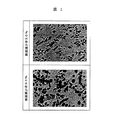
Cuインゴットを大気中にて溶解した後、30体積%の酸化銅(Cu2O)を添加し溶解した。これを金型鋳造した後、温度900℃で押出しを行った。加工度は断面減少率で50〜90%まで行った。1パス毎の断面減少率は5%とし、割れを防止した。断面減少率が大きくなるに連れて、表1に示す様に線膨張係数及び熱伝導率には異方性が生じる。表1に記したL方向とは、延伸方向であり、C方向とは、L方向と垂直な方向を示し、以下同様の表現を用いる。図1にL方向に平行な断面のミクロ組織と断面減少率の関係を示す。また図2にC方向に平行な断面のミクロ組織と断面減少率の関係を示す。50%が100倍,90%が50倍である。断面減少率が大きくなるに連れて、個々の酸化銅は微細になるとともに、アスペクト比はほとんどが3以上で、大きくなり、またその配向方向は延伸方向に近づいていく。図1に示す90%のものの棒径は20μm以下で、1〜10μmがほとんどである。長さは100μm以上のものが15個であった。この視野は710×480μmである。断面減少率が高くなるにつれて、配向はより顕著となり、L方向の熱伝導率が高くなるが、逆にC方向のそれが低くなり、L方向の線膨張係数が大きくなり、逆にC方向のそれは小さくなる。その結果、L方向の熱伝導率は351W/m・Kまで上昇し、C方向との比率が1.05以上で、最大1.77であった。一方、線膨張係数はC方向で10.4×10−6/℃となった。
【0031】
【表1】

(実施例2)
表2にCu−40vol.%Cu2O 組成の線膨張係数と熱伝導率の値を示す。まずCu粉と酸化銅粉を混合した後、冷間プレスして、これを950℃×3時間焼結した後、温度950℃でスエージングを行った。加工度は断面減少率で90%まで行った。図3にL方向に平行な断面の100倍のミクロ組織を示す。その結果、L方向の熱伝導率はC方向のそれより1.75 倍と高く、267W/m・Kまで上昇した。一方、線膨張係数はL方向は大きいがC方向で7.8×10−6/℃と小さくなった。酸化銅の塊となっているものは50μm以下であり、その95%以上は20μm以下である。
【0033】
【表2】
(実施例3)
表3にCu−50vol.%Cu2O 組成の線膨張係数と熱伝導率の値を示す。作製方法は実施例2と同様とした。加工度は断面減少率で90%まで行った。図4にL方向に平行な断面の100倍のミクロ組織を示す。その結果、L方向の熱伝導率はC方向のそれより2.22 倍と高く、218W/m・Kまで上昇した。一方、線膨張係数はC方向で6.1×10−6/℃ となった。酸化銅の塊は100μm以下の大きさであり、塊のほとんどは20μm以下である。
【0035】
【表3】
(実施例4)
実施例3の素材の延伸方向に垂直な面で切出した複合材料の表面をCuめっきした後、Ni電解めっきした放熱板を得た。このとき放熱板の板厚方向と前記酸化銅の長手方向の配向方向とは平行である。このとき放熱板の板厚方向の熱伝導率は267W/m・K、面内の線膨張係数は7.8×10−6/℃ である。本放熱板は、表面にCuめっきによるCu層があるため、モジュールとしてチップを積層した場合、チップからの熱流は、いったん放熱板の面内でCuめっき層全体に広がり、その後板厚方向に拡散する。
【0037】
以後、本発明の銅複合材料を放熱板とした実施例について述べるが、その組織配向はすべて放熱板の板厚方向がL方向のもので、かつCuめっき層を有するものである。
【0038】
(実施例5)
本発明の銅複合材料を、パワー半導体素子の内、IGBT(Insulated Gate Bipolar Transistor;以下IGBTと略す)モジュールの放熱板(ベース板)に適用した実施例を述べる。
【0039】
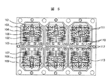
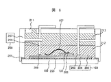
図5はモジュール内部の平面図、図6はモジュールの一部の断面図を示す。
【0040】
IGBT素子1014個とダイオード素子1022個は半田201により銅箔202,203を図示していない銀ろう材でAlN板204に接合したAlN基板103に接続される。AlN基板103上にはエミッタ配線104とコレクタ配線105,ゲート配線106の領域が形成されており、IGBT素子101とダイオード素子102は、コレクタ配線105領域に半田付けされる。各素子からは、金属ワイヤ107によってエミッタ配線104に接続される。また、ゲート配線106領域上には抵抗素子108が配置され、IGBT素子101のゲートパッドから金属ワイヤ107によって抵抗素子108に接続される。半導体素子を搭載したAlN基板103の6基板は、半田206によって本発明の係るCu−Cu2O 合金からなるベース材109に接続される。各絶縁基板間は、端子206と樹脂性のケース207が一体になったケースブロック208の端子206とAlN基板103を半田209によって配線する。また、ケース207とベース109はシリコーンゴム系接着剤210によって接続される。ケースブロック208からの端子接続は、主端子が各AlN基板103上でエミッタ端子接続位置110,エミッタセンス端子接続位置111,コレクタ接続端子位置112が各々2箇所、ゲート端子接続位置113が1箇所で接続される。次に、樹脂注入口を持ったケース蓋211から端子全面が被覆されるようシリコーンゲル212を注入し、その後熱硬化型エポキシ樹脂213を全面に注入してモジュールを完成させる。ベース材109は、酸化銅の長手方向がその平板面と平行に図5の左右に配向しているのが好ましい。
【0041】
表4に一般的に使用されるベース材と、本発明のCu−Cu2O 合金材でCu−40体積%Cu2Oの熱膨張係数と熱伝導率を示す。Cu−Cu2Oベース材料を用いた半導体素子は、一般的に使用されるCuベースのモジュールに比べて熱膨張係数が小さく、AlN基板103とベース109を接続する半田209の信頼性を向上させることができる。その一方で、過酷な使用環境下で半田106の信頼性を向上させるために使用されるMoやAl−SiCベースは、Cu−Cu2Oベースを用いた半導体素子に比べて熱膨張係数は小さいが、熱伝導率も小さく、モジュールの熱抵抗が大きくなる問題が生じる。本実施例のCu−Cu2O ベースを搭載したモジュールでは、信頼性(熱疲労試験寿命)はCuベースに比べ5倍以上、熱抵抗は同じベース厚さのモジュールで、Moベースに比べて0.8 倍以下にすることができる。
【0042】
【表4】
これらの効果により、モジュールの構造や他の部材の選択の幅を拡げることが可能となる。例えば、図5の実施例では、Cu−Cu2O 合金ベース材はMoベース材に比べて熱伝導率が大きい、言い換えれば熱拡がり性が向上するため,動作時の半導体素子端部と中央部の温度差を小さく抑えられる効果があり、半導体素子を従来モジュールに比べ約1.2 倍に大きくしている。これにより、従来素子では同じ電流量を確保するために、IGBTで30個使用していた構造を24で設計が可能になり、モジュールサイズを小型化することができた。さらに、AlNより熱伝導率が約20%小さいアルミナ基板を絶縁基板に使用することが可能になる。アルミナはAlNに比べ抗折強度が強く、基板サイズを大きくすることができる。また、アルミナ板は熱膨張係数がAlN板に比べ大きく、ベース材料との熱膨張差を小さくできるので、モジュール自身の反り量も小さくすることができる。アルミナ基板の使用により、基板の許容サイズを大きくできるので、1枚当りの搭載できる半導体素子数を多くすることができる。つまり、各絶縁板毎に必須な絶縁確保用の面積や基板間の面積を減らすことができ、モジュールサイズを小さくすることが可能である。
【0044】
図7は、本実施例のモジュール製造過程の模式図を示す。(a)Cu−Cu2O ベース109は、表面がNiめっきされ、ほぼ平坦な状態で入荷される。(b)半導体素子101を半田102により接合したAlN基板103を半田205により接合する。この時ベース109の熱膨張係数が半導体素子とAlN基板の複合体より大きいので、半田の冷却過程でモジュール裏面が凹の形状で反る。(c)ケースブロック208を熱硬化型の接着剤で組立てる工程で、半田接合完了の複合体301に比べケースの熱膨張係数が大きいため、接着剤の冷却過程でモジュール裏面がほぼ平坦になる。(d)モジュール内部にシリコーンゲル212,熱硬化型エポキシ樹脂213を充填すると、樹脂の熱膨張係数が大きいためモジュール裏面が凸の形状で反る。
【0045】
図8に、各工程での裏面反り量の実測結果を示す。本発明のCu−Cu2O ベースを使用すると、反り量は従来のMoベースを使用したモジュールに比べると、約1/3に抑えることができる。また、Cuベースの結果は図示していないが、AlN基板との膨張係数差が大きく(b)の工程で裏面が凹の方向で反り量が大きく、モジュール完成後でも裏面が凹で100μm以上の反りが発生する。本発明のCu−Cu2O べースではモジュールの反り量を小さくすることができるのでモジュールの大型化が可能になる。また、組立工程での反り量と同じく、モジュール実働時の温度変化による反りの変化量も小さいので、モジュールと冷却フィンの間に塗布するグリースの流失をおさえることができる。
【0046】
図9に、本発明のモジュールを適用した電力変換装置の一実施例を示す。パワー半導体装置501は、ヒートシンク511上に放熱性グリース510をはさんで締め付けボルト512により実装され、2レベルインバータを構成した例を示す。一般的にモジュール501は、中間点(B点)を一本の中間点配線503で配線できるように左右を反転させて実装する。コレクタ側配線502とエミッタ側配線504は各々u,v,w相を配線して電源電圧509を供給する。信号線は各IGBTモジュール501〜ゲート配線505,エミッタ補助配線506,コレクタ補助配線507によって構成する。508は負荷である。
【0047】
図10及び図11に、モジュールを実装した場合の締め付け前及び後のモジュール裏面の反り量(グリース厚さ)を示し、(a)が本発明、(b)が従来法のものである。従来知られているAl−SiCベースのモジュールの場合、裏面の凸量が約100μmであるが、モジュールをグリースを塗布して締め付けると、締め付け時にグリースに押されて変形し、逆にモジュールの裏面が凹の状態に変形して中央部でのグリース厚さが厚くなり、接触抵抗が大きくなる。これに対して、本発明のCu−Cu2O ベースの場合、初期の裏面の反り量が約50μmであるが、ベース材の剛性が大きいので、グリースを塗布して締め付けた後のモジュール中央部のグリース厚さを約50μmに抑えられ、従来のAl−SiCベースに比べて半減させることができた。さらにモジュール内でのグリース厚さのばらつきも小さくすることができる。実装時のグリースに押されて変形する問題は、Cu−Cu2O 合金よりも剛性の小さなCuベースモジュールの実装時にも当然発生する問題となり、本発明のCu−Cu2O 合金で対策できる。
【0048】
図に示すように、本発明のCu−Cu2O 合金ベースは従来の高信頼性モジュールで適用されていたMoあるいはAl−SiC等のベース材に比べ熱抵抗,接触熱抵抗を小さくすることができることを説明した。それにより、図9に示すようにモジュールを細密の状態で実装できた。さらに、冷却フィンの冷却効率を下げることができるので電力変換装置の実装面積,体積を小さくすることができる。また、グリース厚さを薄くできる事から、冷却フィンの平坦度の許容範囲を大きく設定できるので、大型フィンでの電力変換装置の組立も可能になる。また、強制空冷等の補助冷却機能をなくすこともでき、この点でも小型化,低騒音化を図ることができる。
【0049】
(実施例6)
実施例1〜4に記載の本発明の銅複合材料を放熱板として図12及び図13に示すICを搭載したプラスチックパッケージに適用した。図12は放熱板内蔵型であり、図13は放熱板露出型である。
【0050】
放熱板は、モールド樹脂の熱膨張係数を考慮して、室温から300℃における熱膨張係数が9×10⁻⁶〜14×10−6/℃の範囲となるように、Cu−20〜55体積%Cu2O の範囲内で組成を変えて作製し、機械加工及びNiめっき処理を施して供した。
【0051】
図12でパッケージ構造を説明する。リードフレーム31は、絶縁性ポリイミドテープ32を介して本発明の銅複合材料からなるNiめっきされた放熱板33と接着されている。IC34は放熱板33とはんだにて接合されている。また、Auワイヤ35でIC上のAl電極とリードフレームが接続されている。これらは、リードフレームの一部を除き、エポキシ樹脂,粒径0.5 〜100μmが90重量%以上である球形シリカ製フィラー全体に対して70〜90重量%、および硬化剤を主成分とするモールド樹脂36で封止されている。この樹脂にシリコーンをエポキシ樹脂に対し1〜15重量%含むことが好ましい。図13に示した放熱板露出型のパッケージは、放熱板33がモールド樹脂の外部に露出している点が図12と異なる。
【0052】
上記のようにして実装されたパッケージについて、反りや放熱板とモールド樹脂との接合部分でのクラックの有無を観察した。その結果、モールド樹脂と放熱板との熱膨張差が0.5 ×10⁻⁶/℃以下であれば問題がなく、組成的にはCu−20〜35体積%Cu2O が熱伝導率も200W/m・kと高く、好適であった。放熱板33及びリードフレーム31はいずれも加工方向が図の左右に対応しており、酸化銅が図の左右の方向に伸びたものが好ましい。
【0053】
(実施例7)
図14及び図15は、実施例1〜4に記載の本発明の銅複合材料を放熱板として用い、ICを搭載したセラミックスパッケージの断面図を示す。まず、図14について説明する。IC41はポリイミド系樹脂にてNiめっきされた放熱板42に接合されている。さらに、放熱板42とAl2O3製のパッケージ43は半田により接合されている。パッケージにはCuによる配線がなされ、かつ配線基板との接続用にピン44が設けられている。IC上のAl電極とパッケージの配線とは、Alワイヤ45で接続されている。これらを封止するために、コバール製のウエルドリング46をパッケージにAgろうで接合し、さらにウエルドリングとコバール製のリッド47をローラー電極を用いて溶接した。図15は、図14のセラミックスパッケージに放熱フィン48を接続したパッケージである。放熱板42及び放熱フィン48のいずれも加工方向が図の上下方向であり、酸化銅が上下に伸びたものが好ましい。
【0054】
(実施例8)
図16及び図17は、TAB(Tape Automated Bonding)技術を適用し、かつ実施例1〜4に記載の本発明の銅複合材料を放熱板に使用したパッケージについて説明する。
【0055】
まず、図16のパッケージについて説明する。IC51は熱伝導性樹脂52を介してNiめっきされた本発明に係る放熱板53を接合されている。ICの端子にはAuバンプ54が形成され、TAB55と接続されており、さらにTABは薄膜配線56を経由してリードフレーム57と接続されている。ICはSiゴム58を挿んで、Al2O3製のセラミック基板59,フレーム60、およびシーリングガラス61で密封されている。
【0056】
図17は、樹脂で封止したパッケージである。IC65は、Au−Si合金66により、Niめっきされた本発明に係る放熱板67と接合されており、さらに、熱伝導性樹脂68により銅接地板69及びNiめっきされた本発明に係る放熱板70と接続されている。一方、ICの端子は、Auバンプ71でTAB72と接続され、樹脂73にて封止されている。ここで、リードフレーム及び放熱板の一部は、封止樹脂の外部に露出している。また、TABはエポキシ系Agペースト74で銅接地板に固定されている。放熱板53,70はいずれも酸化銅の加工方向が図面の左右,上下及び奥行方向にいずれも対応できるものである。
【0057】
(実施例9)
図18は、実施例1〜4に記載の本発明の銅複合材料を放熱板に適用したMCMの実施例を示す。IC81はAuワイヤ82を用いて、Niめっきされた本発明に係る放熱板83の上に形成された薄膜配線84に接続され、さらに、AuワイヤでAlN製のパッケージ85上に形成されている配線に接続され、外部端子86として取り出されている。IC部は、42合金製のリッド87とパッケージのWメタライズ層の間にAu−Sn製のプリフォーム88を挿んで接合し、密封されている。
【0058】
放熱板83の酸化銅の長手方向は図の上下方向に配向させるのが好ましい。
【0059】
【発明の効果】
本発明によれば、高熱伝導性を有するCu相と低熱膨張性を有するCu2O 相からなる複合組織を有しており、塑性加工によって伸ばされたCu2O 相の方向性を要求する熱膨張係数及び熱伝導率の目的に合わせて制御可能であるため、半導体装置用放熱板として顕著な効果が達成される。
【図面の簡単な説明】
【図1】本発明の実施例1に係る試料No.1のミクロ組織を示す光学顕微鏡写真。
【図2】本発明の実施例1に係る試料No.1のミクロ組織を示す光学顕微鏡写真。
【図3】本発明の実施例2に係る試料No.4のミクロ組織を示す光学顕微鏡写真。
【図4】本発明の実施例3に係る試料No.5のミクロ組織を示す光学顕微鏡写真。
【図5】本発明の実施例5に係るIGBTモジュールの平面図。
【図6】本発明の実施例5に係るIGBTモジュールの断面図。
【図7】本発明の実施例5に係るIGBTモジュールの製造工程の模式図。
【図8】本発明の実施例5に係るIGBTモジュールの各製造工程でのベース反り量。
【図9】本発明の実施例5に係るIGBTモジュールを実装した電力変換装置の平面図及び断面図。
【図10】本発明の実施例5に係るIGBTモジュールを実装した電力変換装置のモジュールの実装前における反り量。
【図11】本発明の実施例5に係るIGBTモジュールを実装した電力変換装置のモジュールの実装後における反り量。
【図12】本発明の実施例6に係る放熱板内蔵型プラスチックパッケージの断面図。
【図13】本発明の実施例6に係る放熱板露出型プラスチックパッケージの断面図。
【図14】本発明の実施例7に係るセラミックパッケージの断面図。
【図15】本発明の実施例7に係る放熱フィン付きセラミックパッケージの断面図。
【図16】本発明の実施例8に係る半導体装置の断面図。
【図17】本発明の実施例8に係る半導体装置の断面図。
【図18】本発明の実施例9に係るMCMの断面図。
【符号の説明】
21…IGBT素子、22…ダイオード、23…コレクタ電極、24…ゲート電極、25…エミッタ電極、26…AlN製絶縁板、27,33,42,53,67,70…放熱板、31,57…リードフレーム、32…絶縁性ポリイミドテープ、34,41,51,65,81…IC、35,82…Auワイヤー、36…モールド樹脂、43,85…パッケージ、44…ピン、45…Alワイヤ、46…ウエルドリング、47,87…リッド、48…放熱フィン、52,68…熱伝導性樹脂、54…Auバンプ、55…TAB、56,84…薄膜配線、58…Siゴム、59…セラミック基板、60…フレーム、61…シーリングガラス、66…Au−Si合金、69…銅接地板、71…Auバンプ、72…TAB、73…樹脂、74…エポキシ系Agペースト、83…放熱基板、86…外部端子、88…プリフォーム、101…IGBT素子、102…ダイオード素子、103…AlN基板、104…エミッタ配線、105…コレクタ配線、106,505…ゲート配線、107…金属ワイヤ、108…抵抗素子、109…底面金属基板、110…エミッタ端子接続位置、111…エミッタセンス端子接続位置、112…コレクタ端子接続位置、113…ゲート端子接続位置、201,205,209…半田、202…半導体素子側銅箔、203…ベース側銅箔、204…AlN板、206…端子、207…ケース、208…ケースブロック、210…シリコンゴム系接着剤、211…ケース蓋、212…シリコンゲル、213…熱硬化型エポキシ樹脂、301…半導体素子からベース材まで接続した複合体、501…パワー半導体装置、502…コレクタ側配線、503…中間点配線、504…エミッタ側配線、506…エミッタ補助配線、507…コレクタ補助配線、508…負荷(モーター)、509…電源、510…放熱性グリース、511…ヒートシンク、512…モジュール締め付けボルト。[0001]
TECHNICAL FIELD OF THE INVENTION
The present invention relates to a copper composite material having low thermal expansion and high thermal conductivity, and a heat sink and a semiconductor device using the same.
[0002]
[Prior art]
Power electronics is a technology related to conversion and control of power and energy by an electronic device, in particular, a power electronic device used in an on / off mode and a power conversion system as an application technology thereof.
[0003]
For power conversion, various power semiconductor devices having various on / off functions have been used. As this semiconductor device, a rectifier diode having a built-in pn junction and having conductivity in only one direction, and a thyristor, a bipolar transistor, a MOSFET, etc. are put into practical use by various combinations of pn junctions. An insulated gate bipolar transistor (IGBT) and a gate turn-off thyristor (GTO) having a turn-off function by a gate signal have also been developed.
[0004]
These power semiconductor elements generate heat when energized, and the amount of heat generated tends to increase as their capacity and speed increase. In order to prevent the deterioration of the characteristics of the semiconductor element and the shortening of the life of the semiconductor element due to the heat generation, it is necessary to provide a heat radiating section to suppress the temperature rise in the semiconductor element and its vicinity. Copper is generally used as a heat dissipating member because it has a large thermal conductivity of 393 W / m · k and is inexpensive. However, the heat dissipation member of the semiconductor device having the power semiconductor element has a thermal expansion coefficient of 4.2 × 10 -6 Therefore, a heat dissipating member having a coefficient of thermal expansion close to this is desired. Copper has a coefficient of thermal expansion of 17 × 10 -6 / ° C., the solder bonding property with the semiconductor element is not preferable, and a material such as Mo or W having a thermal expansion coefficient close to that of Si is used as the heat radiating member, or provided between the semiconductor element and the heat radiating member.
[0005]
On the other hand, integrated circuits (ICs) in which electronic circuits are integrated on one semiconductor chip are classified into memories, logics, microprocessors, and the like according to their functions. These are called electronic semiconductor elements as opposed to power semiconductor elements. The degree of integration and the operation speed of these semiconductor elements are increasing year by year, and accordingly, the amount of heat generated is also increasing. By the way, electronic semiconductor elements are generally housed in a package for the purpose of shutting it off from the outside air and preventing failure or deterioration. Many of these are a ceramic package in which a semiconductor element is die-bonded to ceramics and hermetically sealed, and a plastic package which is sealed with resin. In addition, a multi-chip module (MCM) in which a plurality of semiconductor devices are mounted on one substrate has been manufactured in order to support high reliability and high speed.
[0006]
The plastic package has a structure in which a lead frame and a terminal of a semiconductor element are connected by a bonding wire, and this is sealed with a resin. In recent years, with an increase in the amount of heat generated by a semiconductor element, a package in which a lead frame has heat dissipation properties and a package in which a heat radiating plate for heat dissipation is mounted have appeared. For heat dissipation, copper-based lead frames and heat sinks with large thermal conductivity are often used,
There is a concern about a defect due to a difference in thermal expansion from Si.
[0007]
On the other hand, the ceramic package has a structure in which a semiconductor element is mounted on a ceramic substrate on which wiring is printed and sealed with a metal or ceramic cap. Furthermore, a composite material of Cu-Mo or Cu-W or a Kovar alloy is bonded to the ceramic substrate and used as a heat sink, but each material has a low thermal expansion or high thermal conductivity and a workability. Improvement and low cost are required.
[0008]
The MCM has a structure in which a plurality of semiconductor elements are mounted as bare chips on a thin film wiring formed on a substrate made of Si, metal, or ceramics, placed in a ceramics package, and sealed with a lid. If heat dissipation is required, a heatsink or heatsink is installed on the package. Copper or aluminum is used as a metal substrate material, which has the advantage of high thermal conductivity, but has a large coefficient of thermal expansion and poor compatibility with semiconductor elements. For this reason, Si or aluminum nitride (AlN) is used for the substrate of the low-reliability MCM. Further, since the heat radiating plate is bonded to the ceramic package, a material having good compatibility with the package material in terms of thermal expansion coefficient and having high thermal conductivity is desired.
[0009]
[Problems to be solved by the invention]
As described above, any semiconductor device on which a semiconductor element is mounted generates heat in its operation, and if the heat is stored, the function of the semiconductor element may be impaired. For this reason, a heat radiating plate having excellent thermal conductivity for dissipating generated heat to the outside is required. Since the heat sink is bonded to the semiconductor element directly or via an insulating layer, the heat sink needs to be consistent with the semiconductor element not only in terms of thermal conductivity but also in terms of thermal expansion.
[0010]
Currently used semiconductor elements are mainly Si and GaAs. Their thermal expansion coefficients are 2.6 × 10 -6 ~ 3.6 × 10 -6 / ° C, 5.7 × 10 -6 ~ 6.9 × 10 -6 / ° C. AlN, SiC, Mo, W, Cu-W, and the like are conventionally known as heat dissipating plate materials having a thermal expansion coefficient close to these, but since these are single materials, the heat transfer coefficient and heat conduction It is difficult to arbitrarily control the rate, and there is a problem that workability is poor and cost is high.
[0011]
Recently, Al-SiC has been proposed as a heat sink material. This is a composite material of Al and SiC. The heat transfer coefficient and the heat conductivity can be controlled in a wide range by changing the ratio of both components, but there is a problem that the workability is very poor and the cost is high. JP-A-8-78578 discloses a Cu-Mo sintered alloy, JP-A-9-181220 discloses a Cu-W-Ni cohesive gold, JP-A-9-209958 discloses a Cu-SiC sintered alloy. Japanese Patent Application Laid-Open No. 9-15773 proposes Al-SiC. These conventionally known powder metallurgy composite materials can control the thermal expansion coefficient and the thermal conductivity over a wide range by changing the ratio of both components, but have low strength and plastic workability, and it is difficult to manufacture thin plates. Further, there are problems such as an increase in cost related to powder production and an increase in the number of production steps.
[0012]
An object of the present invention is to provide a composite material having low thermal expansion, high thermal conductivity, and excellent plastic workability, a semiconductor device using the same, and a heat sink for the same.
[0013]
[Means for Solving the Problems]
The present inventors have made various studies and found that Cu having high thermal conductivity and Cu having low thermal expansion 2 Compound O and Cu 2 It has been found that the above problems can be solved by dispersing
[0014]
The present invention is a composite material having copper and copper oxide, wherein the copper oxide is preferably dispersed in an island shape, and 50% or more of the islands have an aspect ratio of 3 or more and the longitudinal direction is one direction. A composite material characterized by being oriented.
[0015]
The present invention provides a composite material having copper and copper oxide, wherein the copper oxide is dispersed in an island form at 10 to 55% by volume, and 50% or more of the island has an aspect ratio of 3 to 20 and 60% or more. The composite material is characterized in that the longitudinal directions of the islands are oriented in one direction.
[0016]
The present invention provides a composite material having copper and copper oxide, wherein the copper oxide is dispersed in an island form at 10 to 55% by volume, and 50% or more of the island has an aspect ratio of 3 to 20 and 60% or more. The longitudinal direction of the island is oriented in one direction, and the linear expansion coefficient from room temperature to 300 ° C. is 5 × 10 -6 ~ 17 × 10 -6 The composite material is characterized by having a thermal conductivity of 100 to 380 W / m · K at / C.
[0017]
The present invention provides a composite material having copper and copper oxide, wherein the copper oxide is dispersed in an island form at 10 to 55% by volume, and 50% or more of the island has an aspect ratio of 3 to 20 and 60% or more. The longitudinal direction of the island is oriented in one direction, and the linear expansion coefficient from room temperature to 300 ° C. is preferably 5 × 10 -6 ~ 17 × 10 -6 / ° C and the thermal conductivity is 100 to 380 W / m · K, and the thermal conductivity in the orientation direction is higher than the thermal conductivity in the direction perpendicular to the orientation direction, and the ratio is 1.05 to 2.5 times, The difference is preferably 5 to 120 W / m · K, and the linear expansion coefficient from room temperature to 300 ° C. in the orientation direction is larger than the linear expansion coefficient in the direction perpendicular to the orientation direction, preferably 1.1 to 2.0 times. Wherein the composite material is:
[0018]
The present invention is the composite material, wherein eutectic copper oxide is dispersed in copper in the composite material. Further, the composite material has a copper layer having a thickness of 50 μm or less on a surface thereof.
[0019]
The present invention resides in a heat sink for a semiconductor device, comprising the composite material. Further, in the heat sink for semiconductor device, the heat sink for semiconductor device has at least one plating layer of Au, Ni, Pd, Cr, Al, Sn, and Sn-Pb on a surface.
[0020]
According to the present invention, in a semiconductor device having an insulating substrate mounted on a radiator plate and a semiconductor element mounted on the insulating substrate, the radiator plate includes the radiator plate described above.
[0021]
The present invention includes a semiconductor element mounted on a heat sink, a lead frame connected to the heat sink, and a metal wire for electrically connecting the lead frame and the semiconductor element. In a sealed semiconductor device, the radiator plate is formed of the radiator plate described above.
[0022]
The present invention includes a semiconductor element mounted on a heat sink, a lead frame connected to the heat sink, and a metal wire for electrically connecting the lead frame and the semiconductor element. In a semiconductor device which is sealed and is open at least on the side opposite to the bonding surface of the element of the heat radiating plate, the heat radiating plate comprises the heat radiating plate described above.
[0023]
The present invention provides a ceramic multilayer wiring board having a semiconductor element mounted on a heat sink, an external wiring connection pin, and having an open space for accommodating the element in the center, and a terminal of the element and the substrate. A semiconductor device comprising: a metal wire that is electrically connected; joining the radiator plate and the substrate so as to place the element in the space; and joining the substrate with a lid to block the element from the atmosphere. The radiator plate is formed of the radiator plate described above.
[0024]
The present invention provides a ceramic multilayer wiring board having a semiconductor element mounted on a heat sink, a terminal for external wiring connection, and a concave portion for accommodating the element in the center, and electrically connecting the element and the terminal of the substrate. A semiconductor wire for connecting the heat radiating plate and the recess of the substrate so as to place the element in the recess, and joining the substrate by a lid to shield the element from the atmosphere. The radiator plate comprises the radiator plate described above.
[0025]
The present invention includes a semiconductor element joined on a heat sink by a thermally conductive resin, a lead frame joined to a ceramic insulating substrate, and a TAB for electrically connecting the element and the lead frame. In a semiconductor device in which a board and an insulating substrate are joined and the element is shielded from the atmosphere, and a thermally conductive resin elastic body is interposed between the element and the insulating substrate, the heat radiating plate is formed from the heat radiating plate described above. It is characterized by becoming.
[0026]
According to the present invention, a semiconductor element bonded to a first heat sink with a metal, and the first heat sink is mounted on the ground plate of a second heat sink joined to a ground plate; In a semiconductor device including a TAB electrically connected to a terminal and the element sealed with a resin, the radiator plate includes the radiator plate described above.
[0027]
The volume fraction of cuprous oxide may be selected from 10 to 55% by volume in accordance with the desired thermal conductivity and linear expansion coefficient. In addition, the shape of the cuprous oxide is a rod-like island that exists independently of each other and has an aspect ratio of 5 or more. Desirably, the aspect ratio is about 5 to 20. Furthermore, it is desirable that the longitudinal direction of 80% or more of the islands is oriented in one direction, and the variation in the orientation is
It is preferable that it is within 10 °. As described above, by controlling the distribution form of copper oxide rather than simply dispersing it in copper, a composite material having an excellent balance between thermal conductivity and coefficient of linear expansion can be provided. The coefficient of linear expansion and the thermal conductivity from room temperature to 300 ° C can be controlled by the content and the processing rate, and the difference between the thermal conductivity in the orientation direction and the thermal conductivity in the direction perpendicular to the orientation direction can be controlled by controlling the distribution form. The arrangement of the copper oxide in the orientation direction can be determined according to the purpose. Further, in addition to the above, the composite material according to the present invention may have eutectic copper oxide dispersed in copper, and may have a copper layer having a thickness of 50 μm or less on its surface.
[0028]
The composite material according to the present invention is produced by producing a raw material composed of copper and copper oxide by powder metallurgy or casting, then performing plastic working with heat, and finally annealing. The plastic working is preferably performed by a method such as extrusion, rolling, forging, swaging or the like with a reduction in area of 50% or more. The relative density is set to 100%.
[0029]
Further, the heat radiating plate according to the present invention may be cut out from the composite material so that the plate thickness direction is parallel to the orientation direction of the cuprous oxide. As a result, the heat conductivity of the heat sink in the thickness direction is larger than the direction perpendicular thereto, and the coefficient of linear expansion in the plane of the heat sink is smaller than the direction perpendicular thereto. Therefore, the heat radiating plate has improved heat dissipation, and the matching of the linear expansion coefficient with the insulating substrate or the chip is improved, so that the reliability of the module can be improved.
[0030]
BEST MODE FOR CARRYING OUT THE INVENTION
(Example 1)
After dissolving the Cu ingot in the air, 30% by volume of copper oxide (Cu 2 O) was added and dissolved. After casting this in a mold, it was extruded at a temperature of 900 ° C. The working degree was reduced to 50 to 90% in terms of a reduction in area. The cross-sectional reduction rate for each pass was 5% to prevent cracking. As shown in Table 1, anisotropy occurs in the linear expansion coefficient and the thermal conductivity as the cross-sectional reduction rate increases. The L direction described in Table 1 is a stretching direction, and the C direction indicates a direction perpendicular to the L direction, and the same expression is used hereinafter. FIG. 1 shows the relationship between the microstructure of the cross section parallel to the L direction and the reduction rate of the cross section. FIG. 2 shows the relationship between the microstructure of the cross section parallel to the C direction and the cross-sectional reduction rate. 50% is 100 times and 90% is 50 times. As the cross-sectional reduction rate increases, the individual copper oxides become finer, the aspect ratio increases to almost 3 or more, and the orientation direction approaches the stretching direction. The rod diameter of the 90% rod shown in FIG. 1 is 20 μm or less, and most is 1 to 10 μm. The length was 15 pieces having a length of 100 μm or more. This field of view is 710 × 480 μm. As the cross-sectional reduction rate increases, the orientation becomes more remarkable, and the thermal conductivity in the L direction increases. However, the thermal conductivity in the C direction decreases, the coefficient of linear expansion in the L direction increases, and It gets smaller. As a result, the thermal conductivity in the L direction increased to 351 W / m · K, and the ratio to the C direction was 1.05 or more, and was a maximum of 1.77. On the other hand, the coefficient of linear expansion is 10.4 × 10 -6 / ° C.
[0031]
[Table 1]
(Example 2)
Table 2 shows Cu-40 vol. % Cu 2 The values of the linear expansion coefficient and the thermal conductivity of the
[0033]
[Table 2]
(Example 3)
Table 3 shows Cu-50 vol. % Cu 2 The values of the linear expansion coefficient and the thermal conductivity of the
[0035]
[Table 3]
(Example 4)
After the surface of the composite material cut in a plane perpendicular to the stretching direction of the material of Example 3 was plated with Cu, a heat sink having Ni electrolytic plating was obtained. At this time, the thickness direction of the heat sink and the orientation direction of the copper oxide in the longitudinal direction are parallel. At this time, the thermal conductivity of the heat sink in the thickness direction is 267 W / m · K, and the in-plane linear expansion coefficient is 7.8 × 10 -6 / ° C. Since this heat sink has a Cu layer by Cu plating on the surface, when chips are stacked as a module, the heat flow from the chip once spreads over the entire Cu plating layer in the plane of the heat sink, and then diffuses in the plate thickness direction I do.
[0037]
Hereinafter, an example in which the copper composite material of the present invention is used as a heat radiating plate will be described. The texture orientation of the heat radiating plate is such that the thickness direction of the heat radiating plate is the L direction and a Cu plating layer is provided.
[0038]
(Example 5)
The copper composite material of the present invention is used as an IGBT ( I nsulated G ate B ipolar T An embodiment in which the present invention is applied to a radiator (base plate) of a module will be described.
[0039]
FIG. 5 is a plan view of the inside of the module, and FIG. 6 is a sectional view of a part of the module.
[0040]
The 1014 IGBT elements and 1022 diode elements are connected by
[0041]
Table 4 shows commonly used base materials and Cu-Cu of the present invention. 2 O-40 alloy with Cu-40% by volume Cu 2 The thermal expansion coefficient and thermal conductivity of O are shown. Cu-Cu 2 A semiconductor element using an O-based material has a smaller coefficient of thermal expansion than a generally used Cu-based module, and can improve the reliability of the
[0042]
[Table 4]
With these effects, it is possible to expand the range of selection of the module structure and other members. For example, in the embodiment of FIG. 2 Since the
[0044]
FIG. 7 is a schematic view of a module manufacturing process according to the present embodiment. (A) Cu-Cu 2
[0045]
FIG. 8 shows the measurement results of the back surface warpage amount in each step. Cu-Cu of the present invention 2 When the O base is used, the amount of warpage can be suppressed to about 3 as compared with the module using the conventional Mo base. Although the results for the Cu base are not shown, the difference in expansion coefficient from the AlN substrate is large, and the amount of warpage is large in the direction in which the back surface is concave in the step (b). Warpage occurs. Cu-Cu of the present invention 2 With the O base, the amount of warpage of the module can be reduced, so that the module can be made larger. In addition, since the amount of change in the warpage due to the temperature change during the actual operation of the module is small, as in the amount of warpage in the assembly process, the grease applied between the module and the cooling fins can be suppressed from flowing out.
[0046]
FIG. 9 shows an embodiment of a power converter to which the module of the present invention is applied. The
[0047]
FIGS. 10 and 11 show the amount of warpage (grease thickness) on the back surface of the module before and after fastening when the module is mounted. FIG. 10A shows the present invention, and FIG. 10B shows the conventional method. In the case of a conventionally known Al-SiC-based module, the convexity of the back surface is about 100 μm. However, when the module is coated with grease and tightened, the module is deformed by being pressed by the grease during tightening, and conversely, the back surface of the module is Is deformed into a concave state, the grease thickness at the central portion is increased, and the contact resistance is increased. In contrast, the Cu-Cu of the present invention 2 In the case of O-base, the initial back surface warpage is about 50 μm, but the rigidity of the base material is large, so the grease thickness at the center of the module after grease is applied and tightened can be reduced to about 50 μm. Was able to be reduced by half as compared with the Al-SiC base. Further, the variation of the grease thickness in the module can be reduced. The problem of deformation due to being pressed by grease during mounting is Cu-Cu 2 The problem naturally occurs when a Cu-based module having a lower rigidity than the
[0048]
As shown in FIG. 2 It has been described that the
[0049]
(Example 6)
The copper composite material of the present invention described in Examples 1 to 4 was applied to a plastic package on which an IC shown in FIGS. 12 and 13 was mounted as a heat sink. FIG. 12 shows a heat sink built-in type, and FIG. 13 shows a heat sink exposed type.
[0050]
The heat sink has a thermal expansion coefficient of 9 × 10 from room temperature to 300 ° C. in consideration of the thermal expansion coefficient of the mold resin. -6 ~ 14 × 10 -6 / 20 to 55% by volume Cu 2 It was prepared by changing the composition within the range of
[0051]
FIG. 12 illustrates the package structure. The
[0052]
With respect to the package mounted as described above, the presence or absence of warpage and cracks at the joint between the heat sink and the mold resin was observed. As a result, the difference in thermal expansion between the mold resin and the heat sink is 0.5 × 10 -6 / ° C or lower, there is no problem, and the composition is Cu-20 to 35% by volume Cu 2 O 2 was also suitable because of its high thermal conductivity of 200 W / mk. Each of the
[0053]
(Example 7)
FIGS. 14 and 15 are cross-sectional views of a ceramic package having an IC mounted thereon using the copper composite material of the present invention described in Examples 1 to 4 as a heat sink. First, FIG. 14 will be described. The IC 41 is joined to a radiator plate 42 plated with Ni using a polyimide resin. Further, the heat sink 42 and the Al 2 O 3 Package 43 is joined by solder. The package is wired with Cu and provided with
[0054]
(Example 8)
16 and 17 illustrate a package to which a TAB (Tape Automated Bonding) technique is applied and the copper composite material of the present invention described in Examples 1 to 4 is used for a heat sink.
[0055]
First, the package of FIG. 16 will be described. The
[0056]
FIG. 17 shows a package sealed with a resin. The
[0057]
(Example 9)
FIG. 18 shows an example of an MCM in which the copper composite material of the present invention described in Examples 1 to 4 is applied to a heat sink. The
[0058]
It is preferable that the longitudinal direction of the copper oxide of the
[0059]
【The invention's effect】
According to the present invention, Cu phase having high thermal conductivity and Cu phase having low thermal expansion 2 Cu having a composite structure composed of
[Brief description of the drawings]
FIG. 1 shows a sample No. 1 according to Example 1 of the present invention. An optical microscope photograph showing the microstructure of Example 1.
FIG. 2 shows a sample No. 1 according to the first embodiment of the present invention. An optical microscope photograph showing the microstructure of Example 1.
FIG. 3 shows a sample No. 2 according to the second embodiment of the present invention. 4 is an optical microscope photograph showing the microstructure of Example 4.
FIG. 4 shows a sample No. 3 according to a third embodiment of the present invention. 5 is an optical micrograph showing the microstructure of FIG.
FIG. 5 is a plan view of an IGBT module according to
FIG. 6 is a sectional view of an IGBT module according to a fifth embodiment of the present invention.
FIG. 7 is a schematic diagram of a manufacturing process of an IGBT module according to
FIG. 8 shows the amount of base warpage in each manufacturing process of the IGBT module according to
FIG. 9 is a plan view and a cross-sectional view of a power conversion device mounted with an IGBT module according to a fifth embodiment of the present invention.
FIG. 10 shows the amount of warpage of a power converter in which an IGBT module according to a fifth embodiment of the present invention is mounted before mounting the module.
FIG. 11 shows the amount of warpage after mounting the module of the power converter in which the IGBT module according to the fifth embodiment of the present invention is mounted.
FIG. 12 is a sectional view of a plastic package with a built-in heat sink according to a sixth embodiment of the present invention.
FIG. 13 is a cross-sectional view of a heat sink exposed plastic package according to a sixth embodiment of the present invention.
FIG. 14 is a sectional view of a ceramic package according to a seventh embodiment of the present invention.
FIG. 15 is a cross-sectional view of a ceramic package with heat radiation fins according to
FIG. 16 is a sectional view of a semiconductor device according to an eighth embodiment of the present invention.
FIG. 17 is a sectional view of a semiconductor device according to an eighth embodiment of the present invention.
FIG. 18 is a sectional view of an MCM according to a ninth embodiment of the present invention.
[Explanation of symbols]
21 IGBT element, 22 diode, 23 collector electrode, 24 gate electrode, 25 emitter electrode, 26 AlN insulating plate, 27, 33, 42, 53, 67, 70 heat sink, 31, 57 Lead frame, 32: insulating polyimide tape, 34, 41, 51, 65, 81: IC, 35, 82: Au wire, 36: mold resin, 43, 85: package, 44: pin, 45: Al wire, 46 ... weld ring, 47,87 ... lid, 48 ... radiation fin, 52,68 ... thermally conductive resin, 54 ... Au bump, 55 ... TAB, 56,84 ... thin film wiring, 58 ... Si rubber, 59 ... ceramic substrate, Reference numeral 60: frame, 61: sealing glass, 66: Au-Si alloy, 69: copper ground plate, 71: Au bump, 72: TAB, 73: resin, 74: epo Si-based Ag paste, 83: heat dissipation substrate, 86: external terminal, 88: preform, 101: IGBT element, 102: diode element, 103: AlN substrate, 104: emitter wiring, 105: collector wiring, 106, 505: gate Wiring, 107: metal wire, 108: resistance element, 109: bottom metal substrate, 110: emitter terminal connection position, 111: emitter sense terminal connection position, 112: collector terminal connection position, 113: gate terminal connection position, 201, 205 209: solder, 202: semiconductor element side copper foil, 203: base side copper foil, 204: AlN plate, 206: terminal, 207: case, 208: case block, 210: silicone rubber adhesive, 211: case lid , 212: Silicon gel, 213: Thermosetting epoxy resin, 301: From semiconductor element Composite connected to base material, 501: power semiconductor device, 502: collector-side wiring, 503: midpoint wiring, 504: emitter-side wiring, 506: emitter auxiliary wiring, 507: collector auxiliary wiring, 508: load (motor ), 509 power supply, 510 heat radiation grease, 511 heat sink, 512 module bolts.
Claims (8)
Priority Applications (1)
| Application Number | Priority Date | Filing Date | Title |
|---|---|---|---|
| JP37268399A JP3552623B2 (en) | 1999-12-28 | 1999-12-28 | Composite material and heat sink for semiconductor device using the same |
Applications Claiming Priority (1)
| Application Number | Priority Date | Filing Date | Title |
|---|---|---|---|
| JP37268399A JP3552623B2 (en) | 1999-12-28 | 1999-12-28 | Composite material and heat sink for semiconductor device using the same |
Related Child Applications (1)
| Application Number | Title | Priority Date | Filing Date |
|---|---|---|---|
| JP2003142825A Division JP4277582B2 (en) | 2003-05-21 | 2003-05-21 | Semiconductor device |
Publications (2)
| Publication Number | Publication Date |
|---|---|
| JP2001189408A JP2001189408A (en) | 2001-07-10 |
| JP3552623B2 true JP3552623B2 (en) | 2004-08-11 |
Family
ID=18500879
Family Applications (1)
| Application Number | Title | Priority Date | Filing Date |
|---|---|---|---|
| JP37268399A Expired - Fee Related JP3552623B2 (en) | 1999-12-28 | 1999-12-28 | Composite material and heat sink for semiconductor device using the same |
Country Status (1)
| Country | Link |
|---|---|
| JP (1) | JP3552623B2 (en) |
Families Citing this family (1)
| Publication number | Priority date | Publication date | Assignee | Title |
|---|---|---|---|---|
| JP4848539B2 (en) | 2001-08-23 | 2011-12-28 | Dowaメタルテック株式会社 | Heat sink, power semiconductor module, IC package |
-
1999
- 1999-12-28 JP JP37268399A patent/JP3552623B2/en not_active Expired - Fee Related
Also Published As
| Publication number | Publication date |
|---|---|
| JP2001189408A (en) | 2001-07-10 |
Similar Documents
| Publication | Publication Date | Title |
|---|---|---|
| JP3690171B2 (en) | Composite material and its production method and application | |
| US10002821B1 (en) | Semiconductor chip package comprising semiconductor chip and leadframe disposed between two substrates | |
| US10510640B2 (en) | Semiconductor device and method for manufacturing semiconductor device | |
| US7208819B2 (en) | Power module package having improved heat dissipating capability | |
| JP3690278B2 (en) | Composite materials and their uses | |
| US8120153B1 (en) | High-temperature, wirebondless, injection-molded, ultra-compact hybrid power module | |
| CN108735692B (en) | Semiconductor device with a semiconductor device having a plurality of semiconductor chips | |
| US6833617B2 (en) | Composite material including copper and cuprous oxide and application thereof | |
| JP5023604B2 (en) | Semiconductor device | |
| JP2001217363A (en) | Semiconductor device and its heat sink | |
| JP2021111765A (en) | Semiconductor device | |
| JP4277582B2 (en) | Semiconductor device | |
| JP3552623B2 (en) | Composite material and heat sink for semiconductor device using the same | |
| JP2003092383A (en) | Power semiconductor device and its heat sink | |
| WO2023136264A1 (en) | Resin-sealed semiconductor apparatus | |
| JP3938113B2 (en) | Composite materials and their uses | |
| JP3736251B2 (en) | Composite material and method for producing the same | |
| JP2004003023A (en) | Composite material, method for manufacturing the same, and application of the same | |
| US11450623B2 (en) | Semiconductor device | |
| JP2000313905A (en) | Composite material and its various uses | |
| JP2023141693A (en) | Semiconductor device | |
| JP2001210769A (en) | Semiconductor device | |
| JP2023017320A (en) | Semiconductor device | |
| CN116072640A (en) | Low-inductance power module and manufacturing method thereof | |
| JP2000313904A (en) | Composite material, its manufacture and semiconductor device |
Legal Events
| Date | Code | Title | Description |
|---|---|---|---|
| TRDD | Decision of grant or rejection written | ||
| A01 | Written decision to grant a patent or to grant a registration (utility model) |
Free format text: JAPANESE INTERMEDIATE CODE: A01 Effective date: 20040413 |
|
| A61 | First payment of annual fees (during grant procedure) |
Free format text: JAPANESE INTERMEDIATE CODE: A61 Effective date: 20040426 |
|
| FPAY | Renewal fee payment (event date is renewal date of database) |
Free format text: PAYMENT UNTIL: 20080514 Year of fee payment: 4 |
|
| FPAY | Renewal fee payment (event date is renewal date of database) |
Free format text: PAYMENT UNTIL: 20080514 Year of fee payment: 4 |
|
| FPAY | Renewal fee payment (event date is renewal date of database) |
Free format text: PAYMENT UNTIL: 20090514 Year of fee payment: 5 |
|
| FPAY | Renewal fee payment (event date is renewal date of database) |
Free format text: PAYMENT UNTIL: 20100514 Year of fee payment: 6 |
|
| FPAY | Renewal fee payment (event date is renewal date of database) |
Free format text: PAYMENT UNTIL: 20110514 Year of fee payment: 7 |
|
| FPAY | Renewal fee payment (event date is renewal date of database) |
Free format text: PAYMENT UNTIL: 20110514 Year of fee payment: 7 |
|
| FPAY | Renewal fee payment (event date is renewal date of database) |
Free format text: PAYMENT UNTIL: 20120514 Year of fee payment: 8 |
|
| FPAY | Renewal fee payment (event date is renewal date of database) |
Free format text: PAYMENT UNTIL: 20120514 Year of fee payment: 8 |
|
| FPAY | Renewal fee payment (event date is renewal date of database) |
Free format text: PAYMENT UNTIL: 20130514 Year of fee payment: 9 |
|
| FPAY | Renewal fee payment (event date is renewal date of database) |
Free format text: PAYMENT UNTIL: 20130514 Year of fee payment: 9 |
|
| LAPS | Cancellation because of no payment of annual fees |