JP3552374B2 - Signal output device and optical sensor - Google Patents
Signal output device and optical sensor Download PDFInfo
- Publication number
- JP3552374B2 JP3552374B2 JP31318495A JP31318495A JP3552374B2 JP 3552374 B2 JP3552374 B2 JP 3552374B2 JP 31318495 A JP31318495 A JP 31318495A JP 31318495 A JP31318495 A JP 31318495A JP 3552374 B2 JP3552374 B2 JP 3552374B2
- Authority
- JP
- Japan
- Prior art keywords
- light
- light emitting
- light receiving
- sensor
- head
- Prior art date
- Legal status (The legal status is an assumption and is not a legal conclusion. Google has not performed a legal analysis and makes no representation as to the accuracy of the status listed.)
- Expired - Fee Related
Links
- 230000003287 optical effect Effects 0.000 title claims description 57
- 239000013307 optical fiber Substances 0.000 claims description 72
- 238000001514 detection method Methods 0.000 claims description 4
- 239000000835 fiber Substances 0.000 description 33
- 239000011159 matrix material Substances 0.000 description 28
- 230000007423 decrease Effects 0.000 description 10
- 238000010586 diagram Methods 0.000 description 8
- 101100445488 Neurospora crassa (strain ATCC 24698 / 74-OR23-1A / CBS 708.71 / DSM 1257 / FGSC 987) ptr-2 gene Proteins 0.000 description 7
- 238000009429 electrical wiring Methods 0.000 description 5
- WABPQHHGFIMREM-UHFFFAOYSA-N lead(0) Chemical group [Pb] WABPQHHGFIMREM-UHFFFAOYSA-N 0.000 description 5
- 230000005540 biological transmission Effects 0.000 description 4
- 239000000758 substrate Substances 0.000 description 4
- 239000004925 Acrylic resin Substances 0.000 description 3
- 229920000178 Acrylic resin Polymers 0.000 description 3
- 101100215778 Neurospora crassa (strain ATCC 24698 / 74-OR23-1A / CBS 708.71 / DSM 1257 / FGSC 987) ptr-1 gene Proteins 0.000 description 3
- 230000000694 effects Effects 0.000 description 3
- 238000007689 inspection Methods 0.000 description 3
- 238000012423 maintenance Methods 0.000 description 3
- 230000004048 modification Effects 0.000 description 3
- 238000012986 modification Methods 0.000 description 3
- 229920003002 synthetic resin Polymers 0.000 description 3
- 239000000057 synthetic resin Substances 0.000 description 3
- 230000000994 depressogenic effect Effects 0.000 description 2
- 230000002123 temporal effect Effects 0.000 description 2
- 230000000903 blocking effect Effects 0.000 description 1
- 239000011248 coating agent Substances 0.000 description 1
- 238000000576 coating method Methods 0.000 description 1
- 238000000034 method Methods 0.000 description 1
- 239000011347 resin Substances 0.000 description 1
- 229920005989 resin Polymers 0.000 description 1
- 230000000630 rising effect Effects 0.000 description 1
Images


Classifications
-
- G—PHYSICS
- G10—MUSICAL INSTRUMENTS; ACOUSTICS
- G10H—ELECTROPHONIC MUSICAL INSTRUMENTS; INSTRUMENTS IN WHICH THE TONES ARE GENERATED BY ELECTROMECHANICAL MEANS OR ELECTRONIC GENERATORS, OR IN WHICH THE TONES ARE SYNTHESISED FROM A DATA STORE
- G10H1/00—Details of electrophonic musical instruments
- G10H1/32—Constructional details
- G10H1/34—Switch arrangements, e.g. keyboards or mechanical switches specially adapted for electrophonic musical instruments
-
- G—PHYSICS
- G01—MEASURING; TESTING
- G01V—GEOPHYSICS; GRAVITATIONAL MEASUREMENTS; DETECTING MASSES OR OBJECTS; TAGS
- G01V8/00—Prospecting or detecting by optical means
- G01V8/10—Detecting, e.g. by using light barriers
- G01V8/20—Detecting, e.g. by using light barriers using multiple transmitters or receivers
- G01V8/22—Detecting, e.g. by using light barriers using multiple transmitters or receivers using reflectors
-
- G—PHYSICS
- G01—MEASURING; TESTING
- G01D—MEASURING NOT SPECIALLY ADAPTED FOR A SPECIFIC VARIABLE; ARRANGEMENTS FOR MEASURING TWO OR MORE VARIABLES NOT COVERED IN A SINGLE OTHER SUBCLASS; TARIFF METERING APPARATUS; MEASURING OR TESTING NOT OTHERWISE PROVIDED FOR
- G01D5/00—Mechanical means for transferring the output of a sensing member; Means for converting the output of a sensing member to another variable where the form or nature of the sensing member does not constrain the means for converting; Transducers not specially adapted for a specific variable
- G01D5/26—Mechanical means for transferring the output of a sensing member; Means for converting the output of a sensing member to another variable where the form or nature of the sensing member does not constrain the means for converting; Transducers not specially adapted for a specific variable characterised by optical transfer means, i.e. using infrared, visible, or ultraviolet light
- G01D5/32—Mechanical means for transferring the output of a sensing member; Means for converting the output of a sensing member to another variable where the form or nature of the sensing member does not constrain the means for converting; Transducers not specially adapted for a specific variable characterised by optical transfer means, i.e. using infrared, visible, or ultraviolet light with attenuation or whole or partial obturation of beams of light
- G01D5/34—Mechanical means for transferring the output of a sensing member; Means for converting the output of a sensing member to another variable where the form or nature of the sensing member does not constrain the means for converting; Transducers not specially adapted for a specific variable characterised by optical transfer means, i.e. using infrared, visible, or ultraviolet light with attenuation or whole or partial obturation of beams of light the beams of light being detected by photocells
-
- G—PHYSICS
- G10—MUSICAL INSTRUMENTS; ACOUSTICS
- G10H—ELECTROPHONIC MUSICAL INSTRUMENTS; INSTRUMENTS IN WHICH THE TONES ARE GENERATED BY ELECTROMECHANICAL MEANS OR ELECTRONIC GENERATORS, OR IN WHICH THE TONES ARE SYNTHESISED FROM A DATA STORE
- G10H1/00—Details of electrophonic musical instruments
- G10H1/02—Means for controlling the tone frequencies, e.g. attack or decay; Means for producing special musical effects, e.g. vibratos or glissandos
- G10H1/04—Means for controlling the tone frequencies, e.g. attack or decay; Means for producing special musical effects, e.g. vibratos or glissandos by additional modulation
- G10H1/053—Means for controlling the tone frequencies, e.g. attack or decay; Means for producing special musical effects, e.g. vibratos or glissandos by additional modulation during execution only
- G10H1/055—Means for controlling the tone frequencies, e.g. attack or decay; Means for producing special musical effects, e.g. vibratos or glissandos by additional modulation during execution only by switches with variable impedance elements
- G10H1/0553—Means for controlling the tone frequencies, e.g. attack or decay; Means for producing special musical effects, e.g. vibratos or glissandos by additional modulation during execution only by switches with variable impedance elements using optical or light-responsive means
-
- G—PHYSICS
- G10—MUSICAL INSTRUMENTS; ACOUSTICS
- G10H—ELECTROPHONIC MUSICAL INSTRUMENTS; INSTRUMENTS IN WHICH THE TONES ARE GENERATED BY ELECTROMECHANICAL MEANS OR ELECTRONIC GENERATORS, OR IN WHICH THE TONES ARE SYNTHESISED FROM A DATA STORE
- G10H3/00—Instruments in which the tones are generated by electromechanical means
- G10H3/12—Instruments in which the tones are generated by electromechanical means using mechanical resonant generators, e.g. strings or percussive instruments, the tones of which are picked up by electromechanical transducers, the electrical signals being further manipulated or amplified and subsequently converted to sound by a loudspeaker or equivalent instrument
- G10H3/14—Instruments in which the tones are generated by electromechanical means using mechanical resonant generators, e.g. strings or percussive instruments, the tones of which are picked up by electromechanical transducers, the electrical signals being further manipulated or amplified and subsequently converted to sound by a loudspeaker or equivalent instrument using mechanically actuated vibrators with pick-up means
- G10H3/18—Instruments in which the tones are generated by electromechanical means using mechanical resonant generators, e.g. strings or percussive instruments, the tones of which are picked up by electromechanical transducers, the electrical signals being further manipulated or amplified and subsequently converted to sound by a loudspeaker or equivalent instrument using mechanically actuated vibrators with pick-up means using a string, e.g. electric guitar
- G10H3/181—Details of pick-up assemblies
Landscapes
- Physics & Mathematics (AREA)
- Engineering & Computer Science (AREA)
- Acoustics & Sound (AREA)
- Multimedia (AREA)
- General Physics & Mathematics (AREA)
- Life Sciences & Earth Sciences (AREA)
- General Life Sciences & Earth Sciences (AREA)
- Geophysics (AREA)
- Length Measuring Devices By Optical Means (AREA)
- Electrophonic Musical Instruments (AREA)
- Switches Operated By Changes In Physical Conditions (AREA)
Description
【0001】
【発明の属する技術分野】
この発明は、例えば鍵盤楽器における鍵やハンマの動作を検出して信号を出力する信号出力装置およびこれに用いる光センサに関する。
【0002】
【従来の技術】
従来より自動演奏ピアノや消音演奏ピアノなどの鍵盤楽器が提供されており、このような鍵盤楽器では、演奏中の鍵やハンマの動作を検出して信号を出力する演奏情報出力装置を備えている。そして、演奏情報出力装置が出力する信号は、自動演奏ピアノでは、再生演奏時に鍵を駆動するための演奏データとしてフロッピイディスク等の記録手段に記録され、消音演奏ピアノでは、スピーカやヘッドホンから楽音を電子的に発生させるために用いられる。
【0003】
従来、上記のような演奏情報出力装置としては、図13および図14に示すように、鍵1を回動自在に支持する棚板2の上面に機械式スイッチ3(または4)を各鍵1毎に配置したものが知られている。図13に示す機械式スイッチ3は、ゴム接点と呼ばれるもので、内部が中空とされた本体3aの内部に接点3b,3bを配置し、鍵1が押下されると本体3aが上下方向に圧縮されて接点3b,3bが接触して電気的信号を出力するようになっている。
また、図14に示す機械式スイッチ4はリーフスイッチと呼ばれるもので、鍵1が押下されると上側の接点4aが撓んで下側の接点4bに接触して電気的信号を出力するようになっている。
【0004】
また、上記のような機械式スイッチに代えて光センサを用いたキーセンサも供給されている。図15は、フォトインタラプタ5を用いてキーセンサを構成した例であって演奏者側から見た図である。フォトインタラプタ5は、正面視コ字状をなす本体の相対向する壁部の一方にLED5aを収容し、他方の壁部にLED5aが発するビームを受光するフォトトランジスタ5bを収納したものである。一方、鍵1の下面には、シャッタ1aが取り付けられており、鍵1が押下されることによりシャッタ1aがビームを横断する。これによって、フォトトランジスタ5bが出力する電流に変化が生じ、この電流の変化が信号として出力されるようになっている。
【0005】
さらに、図16は本出願人によって開発されたファイバセンサを用いたキーセンサを示す図である。このファイバセンサは、図15に示すものと同様のシャッタ1aに対して交互に配置されたセンサヘッド6と、センサヘッド6に挿入された光ファイバ7とを備えている。センサヘッド6の2つの角部にはプリズム6aと凸レンズ6bとが形成され、プリズム6bは光ファイバ7の光軸に対して45゜傾斜させられている。また、光ファイバ7の自由端の端面はLEDとフォトトランジスタ(図示略)にそれぞれ対向させられている。
【0006】
この構成のもとに、光ファイバ7の端面から出射されたビームは、プリズム6aにおいて内面反射して凸レンズ6bへ向かい、凸レンズ6bから出射する際に屈折してほぼ平行光となる。また、隣接するセンサヘッド6へ向かうビームはその凸レンズ6bに入射して収束させられ、プリズム6aで内面反射して光ファイバ7の端面に入射する。そして、押鍵によりシャッタ1aが図中紙面と直交する方向へ移動すると、シャッタ1aがビームを横断し、これによって、フォトトランジスタbが出力する電流に変化が生じて信号として出力されるようになっている。
【0007】
以上が従来の演奏情報出力装置のうち鍵の操作を検出するキーセンサの構成であり、演奏情報出力装置は、いずれの機械式スイッチや光センサからの信号を受信したかにより当該押鍵に係る鍵を検出するようになっている。
ところで、ピアノには鍵が88個あるため、全ての光センサ等の出力を各キーセンサ毎に設けた受信用ポートから個別に入力するようにすると、受信用ポートが88個必要となって装置が極めて複雑となる。そこで、従来においては、光センサ等への入力系統と出力系統を分けてマトリクススイッチを構成してキースキャンを行うようにしている。
【0008】
図17は、図13または図14に示す機械式スイッチ3または4(以下、スイッチと略称する)によってマトリクススイッチを構成した例を示す図である。図17のマトリクススイッチを構成する横線は、各スイッチの一方の端子が接続された入力回路を示し、縦線は他方の端子が接続された出力回路を示す。また、横線と縦線との交差部に鍵の鍵盤番号を付して各鍵盤番号に対応するスイッチの配置を示している。
【0009】
ここで、ピアノの音は鍵盤番号#1から#12までが(A)の音から(G#)の音までであり、これらの音をひとまとめにして1オクターブと称すると、ピアノでは8オクターブの音まである。図17に示したマトリクススイッチでは、同じオクターブに属するスイッチを縦線に沿って配置して示し、同じ音の種類(A,A#,…,G#)に属するスイッチを横線に沿って配置して示している。なお、12種類の音に対して8オクターブとすると、全部で96個の音が存在することになるが、実際には、ピアノの8オクターブでは(A)から(C)までの4つの音だけであり、ピアノの鍵盤番号は#88までである。よって、図17には、鍵盤番号#88のスイッチまで記載した。また、説明の便宜上、同じ種類の音に属することを指す際に、ノートナンバーa(A)、ノートナンバーb(A#)(ノートナンバーa〜ノートナンバーl)などと称することにする。
【0010】
さて、このキーセンサは、マトリクススイッチの横線で示される入力回路にキースキャン信号を出力する送信部Trと、縦線で示される出力回路から信号が入力される受信部Reとを備えている。キースキャン信号は、一定の極めて短い周期を持ったパルス電流であり、ノートナンバーaに属する入力回路からノートナンバーlに属する入力回路まで重複することなく順番に繰り返し出力される。
今、鍵盤番号#3の鍵が押下されたとすると、この鍵に設けられたスイッチが押されて導通状態となる。そして、スイッチが導通している間に、キースキャン信号のうちノートナンバーcの入力端子に対して出力するものが巡ってくると、その瞬間に、その信号が1オクターブに属する出力回路から受信部Reに入力される。そして、受信部Reは、ノートナンバーcの入力端子への出力タイミングで1オクターブの出力端子から信号が入力されたことにより、押下された鍵が鍵盤番号#3のものであることを検出する。
このように、この演奏情報出力装置では、受信部Reが信号を入力したタイミングが示すノートナンバーと、信号を入力した出力端子が示すオクターブとによって押下された鍵を検出することができる。また、スイッチが導通状態になるタイミングと、受信部Reに信号が入力されるタイミングにずれが生じるが、そのずれは極めて短時間であるため何ら支障は生じない。
【0011】
次に、図18は図15に示すフォトインタラプタによってマトリクススイッチを構成した例を示す。この図に示すマトリクススイッチは、図17のスイッチをフォトインタラプタ5に代えたものであり、キースキャンの動作も図17に示すものと同じである。
また、図19は、図16に示すファイバセンサ6によってマトリクススイッチを構成した例であって、直線状に配置されたファイバセンサ6を1オクターブ毎に行を変えてマトリクス状に配置した状態を示す。この例では、送信部にLEDがノートナンバーaからノートナンバーlまで12個設けられ、受信部にフォトトランジスタPTrが1オクターブから8オクターブまで8個設けられている。なお、ファイバセンサどうしの中間に付した数字は、これらファイバセンサによって検出される鍵の鍵盤番号を示す。
【0012】
図19に示すように、各ファイバセンサの受光側の光ファイバは、オクターブ毎に束ねられてそれらの端面を受信部のフォトトランジスタPTrに対向させている。各オクターブには、12個のノートナンバーが存在するから、各フォトトランジスタRTrにはそれぞれ12本の光ファイバの端面が対向している。ただし、鍵盤番号は#88までであるため、8オクターブに属するフォトトランジスタRTrに対向する光ファイバは4本である。
また、各ファイバセンサの発光側の光ファイバは、ノートナンバー毎に束ねられて送信部のLEDにそれらの端面を対向させている。鍵盤番号は1オクターブから8オクターブまであるから、各LEDにはそれぞれ8本の光ファイバの端面が対向している。ただし、鍵盤番号は#88までであるため、ノートナンバーeからノートナンバーlまでに属するLEDに対向する光ファイバはそれぞれ7本である。
【0013】
このキーセンサでは、送信部のLEDからキースキャン信号が出力される。キースキャン信号は、一定の極めて短い周期を持った光パルスであり、ノートナンバーaに属するLEDからノートナンバーlに属するLEDまで重複することなく順番に繰り返し出力される。1つのLEDから光パルスが発せられると、この光パルスは8つの発行側の光ファイバを伝達して各ファイバセンサに送られる。そして、隣接するファイバセンサに送られた光パルスのビームは、受光側の光ファイバを伝達して1オクターブから8オクターブまでに属する各フォトトランジスタPTrに受光され、各フォトトランジスタPTrは受けた光の量に対応する電流を発生する。
【0014】
今、鍵盤番号#2の鍵が押下されたとすると、この鍵に設けられたシャッタ1aが2つのファイバセンサ6,6の間に移動する。そして、シャッタ1aがビームの光路上に位置している間に、キースキャン信号のうちノートナンバーbの発光側光ファイバに対して出力するものが巡ってくると、1オクターブに属するフォトトランジスタPTrに受光されるべきビームがシャッタ1aによって遮られ、このフォトトランジスタPTrが出力する電流が小さくなる。そして、受信部は、ノートナンバーbの発行側光ファイバへの出力タイミングで、1オクターブに属するフォトトランジスタPTrの出力電流が所定の閾値を下回ったことにより、押下された鍵が鍵盤番号#2のものであることを検出する。
【0015】
このように、このキーセンサでは、特定のフォトトランジスタPTrの出力電流が所定の閾値を下回ったタイミングが示すノートナンバーと、当該フォトトランジスタが属するオクターブとによって押下された鍵を検出することができる。また、上記のようなキーセンサをシャッタの進行方向に沿って2列配置することにより、シャッタが最初のビームを遮った時刻と次のビームを遮った時刻から、押鍵速度を算出するようにしたものも提供されている。
【0016】
【発明が解決しようとする課題】
しかしながら、上記のようなファイバセンサを用いてキースキャンを行うキーセンサにおいても、以下のような改善点があった。
▲1▼ファイバセンサが88個必要であるため発行側と受光側とでそれぞれ88本もの光ファイバを必要とし、特に、キーセンサを2列配置した構成では、光ファイバの本数が倍になる。このため、ファイバセンサ等の組付け作業に多くの労力を必要とし、保守点検作業も煩雑となる。もちろん、機械式スイッチを用いてキースキャンを行う演奏情報出力装置においても、配線作業や保守点検作業が煩雑になるという同じ課題がある。
▲2▼ファイバセンサのプリズムは光を内面反射する構成であるため、入射した光のうち臨界角以内の角度で入射したものだけを反射する。上記構成のファイバセンサでは、光ファイバから発せられた光が拡大しながらプリズムに達するため、光の一部が臨界角を越える入射角でプリズムに入射する。よって、光の一部しか使用されないために効率が悪いという欠点がある。
【0017】
よって、本発明は上述した事情に鑑みてなされたもので、光ファイバや電気配線の数を大幅に低減することができる信号出力装置を提供することを目的としている。また、本発明は、光を有効に使用することができる光センサを提供することも目的としている。
【課題を解決するための手段】
【0018】
請求項1に記載の信号出力装置は、発光手段から出射したビームを受光手段に入射させる光路を有しており、上記発光手段と上記受光手段との間にある光路を移動体が遮ったか否かを検出し、該検出に応じた信号を出力する信号出力装置において、上記発光手段に光を発生させるための信号を出力する送信部と、上記受光手段が受光した光を信号として受信する受信部とを設け、上記発光手段は、1つの発光部から2つの移動体に対して光を出射し、上記受光手段は、2つの発光手段から出射された光を1つの受光部で受光し、上記発光手段と上記受光手段とを複数交互に配設するとともに、1つの発光手段から出射された2つの光を異なる受光手段で受光するように配設し、上記送信部は、複数の発光手段について各々異なるタイミングで発光させるようにしたことを特徴としている。
【0019】
請求項2に記載の光センサは、発光部と、該発光部と離間した位置に設けられた受光部と、上記発光部から出射された光を上記受光部に入射させる光路上に並設され、光を透過する複数のセンサヘッドとを備え、該センサヘッド間の光路を移動体が遮ったか否かを検出する光センサであって、上記センサヘッドは、光を透過する部材によって略矩形状に形成されており、両隣に設けられたセンサヘッドと対向する2つの側面と、上記発光部または上記受光部と対向する1の面と、上記1の面と対向する面をV字状に切り欠いて形成された1対の反射面とを有し、上記発光部から出射され、上記1の面の側から入射された光を上記1対の反射面により内面反射させて上記2つの側面から両隣のセンサヘッドに向けて出射する一方、両隣のセンサヘッドの側面から出射され、上記2つの側面から各々入射された光を上記1対の反射面により内面反射させて上記1の面の側に出射し、上記受光部に入射させることを特徴としている。
【0020】
請求項3に記載の光センサは、請求項2において、前記1対の反射面が、前記発光部から発せられた光を両側へほぼ均等に内面反射させることを特徴としている。
【0021】
請求項4に記載の光センサは、請求項2または3において、前記センサヘッドに、前記一対の反射面の境界部へ向けて光を出射する発光素子か、または、センサヘッドの両側から入射して上記1対の反射面で内面反射した光を受光する受光素子を設けたことを特徴としている。
【0022】
請求項5に記載の光センサは、請求項2または3において、前記センサヘッドに、前記一対の反射面の境界部へ向けて光を出射するか、または、センサヘッドの両側から入射して上記1対の反射面で内面反射した光を受光する光ファイバの端部を設けたことを特徴としている。
【0023】
請求項6に記載の光センサは、発光手段と受光手段とを互いに離間して交互に設け、前記発光手段に、電流が供給されることによりその両隣に配置された受光手段へ向けて光を発する一対の発光素子を設け、上記受光手段に、その両隣に配置された上記発光手段からの光を受けることにより電気的信号を出力する一対の受光素子を設けたことを特徴としている。
【0024】
請求項1に記載の信号出力装置にあっては、発光手段は1つの発光部から2つの移動体に対して光を出射し、受光手段は2つの発光手段から出射された光を1つの受光部で受光するが、1つの発光手段から出射された2つの光を異なる受光手段で受光するように発光手段と受光手段を配設するとともに、複数の発光手段を各々異なるタイミングで発光させるようにした。これにより、発光手段から受光手段へ向かう光が遮られたタイミングによって当該光を発した発光手段が特定されるとともに、そのタイミングで受光可能な複数の受光手段のうち実際に受光した受光手段が何れであるかによって受光手段が特定できる。
【0025】
また、請求項2に記載の光センサにあっては、発光部から発せられた光がほぼV字状をなして隣接する反射部で両側へ振り分けるように内面反射するから、1つの発光部の光を2つの方向へ出射させることができる。また、2つの発光部から入射した光を1つの受光部へ受光させることができる。よって、この光センサを請求項1に記載の構成に用いることにより、光ファイバや電気配線の数を大幅に低減した演奏情報出力装置を構成することができる。
また、請求項3に記載の光センサにあっては、発光部から発せられた光の光軸は反射部どうしの二等分線にほぼ一致するから、各反射部へ入射する光の入射角が小さい。よって、反射部どうしのなす角度を適宜設定することにより、反射部へ入射する光の入射角を臨界角以下にして全反射させることができるので、光を有効に使用することができる。
【0026】
さらに、請求項6に記載の光センサにあっても、一対の発光素子が発する光を両側に向かわせることができ、また、両側の発光素子が発する光を一対の受光素子で受けることができるので、請求項1に記載の構成に用いることにより、光ファイバや電気配線の数を大幅に低減した演奏情報出力装置を構成することができる。
【0027】
【発明の実施の形態】
(1)第1の実施の形態
A.キーセンサの構成
以下、図1ないし図4を参照して本発明の第1の実施の形態について説明する。
図1は実施の形態のキーセンサ(演奏情報出力装置)を示す下面図であり、このキーセンサは、自動演奏ピアノや消音演奏ピアノなどの鍵盤楽器の鍵盤の下側に取り付けられるようになっている。図1において符号10は長尺の板状をなすフレームであり、その長手方向を鍵盤楽器の幅方向へ向けて配置される。フレーム10には、複数のスリット11,…が各鍵1の位置に形成されている。そして、押鍵が行われると鍵1の演奏者側の端部が下降し、鍵1の下面に取り付けたシャッタ1aがスリット11内に挿入されるようになっている。
【0028】
フレーム10にはセンサヘッド20がスリット11,11の中央に位置して固定されている。センサヘッド20は、アクリル樹脂などの透明な合成樹脂で外観略矩形状に形成されている。センサヘッド20の一側は90゜をなすV字状に切り込まれ、その両側には平面視三角形状のプリズム21,21が形成されている。また、センサヘッド20のスリット11側の側部には、凸球面状をなすレンズ22が形成されている。プリズム21,21の傾斜面(反射部)の交差部は、レンズ22の直径線上に位置している。さらに、センサヘッド20の他側中央部には、光ファイバ25が挿入されている。光ファイバ25は、アクリル樹脂などの透明な合成樹脂で形成された直径0.5mm程度の1本の線材で構成され、その光軸は、傾斜面21a,21aの二等分線とほぼ一致している。
【0029】
各光ファイバ25の自由端の端面は、LEDとフォトトランジスタPTr(図3参照)とに交互に対向させられている。これにより、LEDが発する光は、光ファイバ25を伝達してセンサヘッド20の内部へ出射する(以下、このセンサヘッド20を発光ヘッド20aと称する)。そして、出射した光は、発光ヘッド20aのプリズム21で内面反射してレンズ22へ向かい、平行なビームとなってレンズ22から出射する。このビームは、隣接するセンサヘッド20(以下、このセンサヘッド20を受光ヘッド20bと称する)のレンズ22に入射し、レンズ22で収束させられつつプリズム21で反射して光ファイバ25の端面に入射する。入射した光は光ファイバ25を伝達してフォトトランジスタPTrに受光され、フォトトランジスタPTrは受光した光の量に対応する電流を出力する。
【0030】
このように、この実施の形態のキーセンサでは、発光ヘッド20aと受光ヘッド20bが交互に配置され、1つの受光ヘッド20bによってその両側の鍵1の押鍵を検出するようになっている。そのために、光ファイバ25によりマトリクススイッチを構成してキースキャンを行うように構成されている。以下、マトリクススイッチの構成について図3および図4を参照して説明する。
【0031】
B.マトリクススイッチの構成
図3に示すように、このキーセンサは、図中aからlまでの符号を付した12個のLEDを有する送信部と、1から8までの符号を付した8個のフォトトランジスタPTrを有する受信部とを備えている。なお、以下の説明においてLEDまたはフォトトランジスタPTrのいずれかを特定して指す場合には、「LEDa」、「PTr1」というようにグループを示す添字を付して説明する。また、発光ヘッド20aおよび受光ヘッド20bのいずれかを特定して指す場合には、「発光ヘッド20a1」というように、その右隣に配置された鍵の鍵盤番号を添えて説明する。
【0032】
各LEDには、4個または3個の発光ヘッド20aの光ファイバが束ねられてそれらの端面が対向させられている。すなわち、LEDaには、2オクターブづつ離れた4つの発光ヘッド20a1,20a25,20a49,20a73の光ファイバが接続されている。また、LEDbには、2オクターブづつ離れた4つの発光ヘッド20a3,20a27,20a51,20a75の光ファイバが接続されている。表1は、図4に示す発光ヘッド20aの接続状態をまとめたものである。なお、図4の○印は発光ヘッド20a、●印は受光ヘッド20bを示し、発光ヘッド20aと受光ヘッド20bの間の数字は、そこに配置された鍵の鍵盤番号を示す。また、鍵の個数は88であるため、発光ヘッドは45個、受光ヘッドは44個となっている。また、最も右端に位置する発光ヘッド20aの番号を89としたが、鍵盤番号#89は存在しない。
【0033】
【表1】

表1から判るように、LEDには2オクターブ飛びで発光ヘッド20aの光ファイバが接続され、次のLEDには、前者に対して2つづつずれた発光ヘッド20aの光ファイバが接続されている。また、LEDaからLEDiまでは、それぞれ4つの発光ヘッド20aの光ファイバが接続され、LEDjからLEDlまでは、発光ヘッド20aが#89までであることから、それぞれ3つの発光ヘッド20aの光ファイバが接続されている。したがって、前述のように、発光ヘッド20aの光ファイバは全部で45本となっている。
【0035】
次に、受光ヘッド20bの光ファイバの接続について説明する。各フォトトランジスタPTrには、6個または4個の受光ヘッド20bの光ファイバが束ねられてそれらの端面が対向させられている。すなわち、フォトトランジスタPTr1には、鍵盤番号で4づつ離れた6つの受光ヘッド20b2,20b6,20b10,20b14,20b18,20b22の光ファイバが接続されている。また、フォトトランジスタPTr2には、鍵盤番号で4づつ離れた6つの受光ヘッド20b4,20b8,20b12,20b16,20b20,20b24の光ファイバが接続されている。表2は、図4に示す受光ヘッド20bの接続状態をまとめたものである。
【0036】
【表2】
表2から判るように、フォトトランジスタPTrには4つ飛びで受光ヘッド20bの光ファイバが接続され、次のフォトトランジスタPTrには、前者に対して2つづつずれた受光ヘッド20bの光ファイバが接続されている。また、フォトトランジスタPTr1からPTr6までは、それぞれ6つの受光ヘッド20bの光ファイバが接続され、フォトトランジスタPTr7およびPTr8は、それぞれ4つの受光ヘッド20bの光ファイバが接続されている。したがって、前述のように、受光ヘッド20bの光ファイバは全部で44本となっている。
【0038】
C.実施の形態の動作
▲1▼センサヘッドの作用
まず、送信部のLEDからキースキャン信号が出力される。キースキャン信号は、一定の極めて短い周期を持った光パルスであり、LEDaからLEDlまで間断なく順番に繰り返し出力される。この光パルスは、図1に示すように、光ファイバ25を伝わって発光ヘッド20a内に出射される。ここで、光ファイバ25から出射された光は、発光ヘッド20a内で拡大しながらプリズム21,21へ入射し、プリズム21,21の傾斜面21a,21aで内面反射してほぼ均等に左右へ振り分けられる。傾斜面21a,21aで内面反射した光はその後も拡大を続けるが、レンズ22から出射する際に屈折してほぼ平行なビームとなる。このビームの断面は、図2にドットで示すように略半円状をなしている。なお、ビームの断面が完全な半円状をなしていないのは、光ファイバ25の光軸から半径方向へ離れた箇所から出射した光が、傾斜面21a,21aの境界の近傍でレンズ22の直径線よりも外側へ、すなわち、図1のレンズ22の中心線よりも下側へ向けて反射するからである。
【0039】
次に、発光ヘッド20aのレンズ22から出射したビームは、両隣の受光ヘッド20bのレンズ22,22に入射し、その際に屈折して収束しながらプリズム21の傾斜面21aで内面反射する。そして、内面反射した光は収束しながら光ファイバ25の端面に入射し、光ファイバを伝わってフォトトランジスタPTrに受光される。これにより、フォトトランジスタPTrは、受光した光の量に対応する電流を発生する。
【0040】
ここで、鍵1が押下されると、その鍵1に設けられたシャッタ1aがスリット11に挿入され、発光ヘッド20aから受光ヘッド20bへ向かうビームの光路に進入してくる。一方、ビームは極めて短い周期で断続的に発生させられるから、シャッタ1aが光路に進入すると直ちにビームに干渉する。これにより、その受光ヘッド20bが接続されたフォトトランジスタPTrが受光する光の量が減少し、フォトトランジスタPTrが出力する電流が減少する。そして、フォトトランジスタPTrが発生する電流が所定の閾値を下回ることにより、キーセンサは押鍵を検出する。
【0041】
▲2▼キースキャンの動作
次に、このキーセンサにおけるキースキャンの動作について図4を参照して説明する。なお、以下の説明において、特定の鍵盤番号の鍵を指すときは、鍵#1というように鍵盤番号を添えて説明する。
送信部のLEDa〜lは、その順番で極めて短い周期で間断なく光パルス信号の出力を繰り返す。1つのLEDa〜lが光パルス信号を出力すると、その光は表1に示す発光ヘッド20aに伝達され、発光ヘッド20aからその両隣の受光ヘッド20b,20bに光ビームが出射される。
今、鍵#3が押下されたとすると、そのシャッタ1aは発光ヘッド20a3と受光ヘッド20b4の間を通過してビームに干渉する。これにより、受光ヘッド20b4が接続されたフォトトランジスタPTr2が受光する光の量が減少し、フォトトランジスタPTr2は信号を出力する。
【0042】
鍵#3が押下されることにより、LEDbが光パルスを発したタイミングでフォトトランジスタPTr2が信号を出力するから、まず、表1に示す発光ヘッド20a3〜75が特定される。次に、フォトトランジスタPTr2が信号を出力したことにより、表2に示す受光ヘッド4〜24が特定される。ここで、隣接する一対の発光ヘッド20aおよび受光ヘッド20b間のビームが遮られることにより、フォトトランジスタPTr2が信号を出力したのであるから、表1および表2により隣接したものを探すと、発光ヘッド20a3と受光ヘッド20b4しか存在しない。これにより、発光ヘッド20a3と受光ヘッド20b4の間の鍵#3が特定され、キーセンサは、鍵#3による押鍵がなされたことを示すキーコードとともに、フォトトランジスタPTr2が信号を出力したタイミングで例えばキーオン信号を出力する。
【0043】
上記構成のキーセンサにおいては、上述したようなキースキャンを行うことにより、各センサヘッド20に接続する光ファイバ25が1本であっても全ての鍵を別個に検出することができる。したがって、光ファイバ25の本数が従来の半分となり、キーセンサの組立作業や保守点検作業を大幅に低減することができる。
また、光ファイバ25の光軸に線対称となるようにプリズム21,21を形成しているので、光ファイバ25から発した光が均等に両側へ振り分けられるとともに、両隣の発光ヘッド20aから受光したビームが光ファイバ25へ収束させられる。したがって、上述のようなキースキャン方式が可能になるとともに、光のプリズム21への入射角が臨界角よりも小さい48゜以下となるので、光が全反射し、よって、光を有効に利用することができる。
【0044】
(2)第2の実施の形態
A.第2の実施の形態の構成
次に、図5および図6を参照して本発明の第2の実施の形態について説明する。第2の実施の形態は、光ファイバをセンサヘッドに対して離間して設けたファイバサポートに取り付けた点のみが前記実施の形態と異なっている。そこで、以下の説明においては、前記実施の形態と同等の構成要素には同符号を付してその説明を省略する。
図において符号30はセンサヘッドである。センサヘッド30はアクリル樹脂などの透明な合成樹脂で外観略矩形状に形成されている。センサヘッド30の一側は90゜をなすV字状に切り込まれ、その両側には平面視三角形状のプリズム31,31が形成されている。また、センサヘッド30の他側には、凸球面状をなすレンズ32が形成されている。
【0045】
次に、フレーム10には、各センサヘッド30から離間した発行側ファイバサポート40と、受光側ファイバサポート50が交互に配置されている。発光側ファイバサポート40は矩形状をなす本体41の一側に、半円柱状をなすレンズ42を形成して構成されている。発行側ファイバサポート40の本体41の他側には、光ファイバ25が挿入され、光ファイバ25の端面はレンズ42に臨んでいる。
【0046】
また、受光側ファイバサポート50は矩形状をなす本体51の一側に、凸球面状をなすレンズ52を形成して構成されている。受光側ファイバサポート50の本体51の他側には、光ファイバ25が挿入され、光ファイバ25の端面はレンズ52に臨んでいる。なお、以下においては、発光側ファイバーサポート40に対向するセンサヘッド30を発光ヘッド30aと称し、受光側ファイバーサポート50に対向するセンサヘッド30を受光ヘッド30aと称して説明する。また、各光ファイバ25は図3および図4に示すように送信部と受信部に接続されており、上述したと同じキースキャンが行われるようになっている。
【0047】
B.第2の実施の形態の動作
光ファイバ25から発せられた光は、発行側ファイバサポート40のレンズ42によって縦横が異なる出射角で屈折させられる。すなわち、レンズ42から出射した光は、縦方向については大きな広がりをもって拡大するが、横方向については内側へ向けて屈折させられるため、広がりは小さい。その結果、レンズ42を出射した光の横断面は縦長のほぼ楕円形をなす。そして、発行側ファイバサポート40と発光ヘッド30aとの距離、および発光ヘッド30aの正面視形状(矩形状)を適宜選定することにより、光が発光ヘッド30aに入射するときの断面に発光ヘッド30aがほぼ内接するようになっている。したがって、発光ヘッド30aに入射する光の横断面は、楕円形の4側がカットされた矩形状をなすことになる。
【0048】
発光ヘッド30aに入射した光は、レンズ32で屈折してほぼ平行光となってプリズム31へ向かう。そして、光は、プリズム31で内面反射(この場合も全反射である)することにより左右に均等に振り分けられ、発光ヘッド30aの両側面から平行なビームとなって出射する。図6のドットで示す部分は、発光ヘッド30aから出射するビームの横断面であり、縦長の矩形状をなしている。このビームは、受光ヘッド30bに入射するとプリズム31で内面反射し、レンズ32で収束させられて発光側ファイバサポート50のレンズ52に入射する。そして、レンズ52でさらに収束させられて光ファイバ25の端面に入射する。
【0049】
上記構成の光センサにあっては、鍵が押下されてシャッタ1aがビームの光路に進入すると、前述したと同様に間欠的に発生するビームにシャッタ1aが干渉する。これにより、受光側ファイバサポート50の光ファイバ25が接続されたフォトトランジスタの受光量が低下し、フォトトランジスタが出力する電流が受光量に応じて低下する。このビームの後に次のビームが発せられる間隔は極めて短いから、実質的にはビームは連続して発せられるのと同じである。したがって、下降するシャッタ1aにより、フォトトランジスタが受光する光の量が連続的に減少してゆく。
【0050】
このように、シャッタ1aがビームの光路中を横断しているときは、フォトトランジスタが受光する光の量が連続的に減少し、フォトトランジスタの出力電流がその都度減少してゆく。したがって、このキーセンサでは、フォトトランジスタの出力電流の時間的変化に基づいて、シャッタ1aすなわち鍵1の位置の時間的変化を求めることができ、これにより押鍵速度を求めることができる。
特に、この実施の形態では、発光側ファイバサポート40のレンズ42によって光の断面形状が縦長の楕円形とされ、しかも、発光ヘッド30aに達するまでに大きく拡大させられるから、ビームの縦方向長さを充分に確保して上昇端から下降端までの鍵の動きの全域にわたって鍵の動作を精密に検出することができる。しかも、ビームが矩形状であるため鍵の移動量に対するフォトトランジスタの出力信号が線形となるから、出力信号の取扱を容易にすることができる。
【0051】
(3)第3の実施の形態
A.光センサの構成
次に、図7を参照して本発明の第3の実施の形態について説明する。第3の実施の形態は、光センサをフォトインタラプタと同等に構成したことを特徴としている。図7に示すように、発光ヘッド60は外観略矩形状をなし、その一側は90゜をなすV字状に切り込まれて両側に平面視三角形状のプリズム61,61が形成されている。また、発光ヘッド60の左右の側部には、凸球面状をなすレンズ62が形成されている。発光ヘッド60のプリズム61,61と反対側の側部には、発光素子64を有する基体63が埋設されている。基体63の一側には円錐状の反射面63aが形成され、反射面63aの底部に発光素子64が固定されている。なお、図中符号65は発光素子64に接続されたリード線である。
【0052】
次に、受光ヘッド70は、発光ヘッド60と同等に形成されたプリズム71,71およびレンズ72を有している。受光ヘッド70のプリズム71,71と反対側の側部には、フォトトランジスタ等の受光素子74を有する基体73が埋設されている。受光素子73の一側には円錐状の集光面73aが形成され、反射面73aの底部に受光素子74が固定されている。なお、図中符号75は受光素子74に接続されたリード線である。
【0053】
上記のように構成された発光ヘッド60および受光ヘッド70は、図1に示すものと同様にフレームに交互に配置される。なお、このような構成の発光ヘッド60および受光ヘッド70の本体は、可視光カットフィルター付の樹脂で形成した方が外乱光の影響を防止する上で望ましい。また、各発光ヘッド60と受光ヘッド70のリード線65,75は、マトリクススイッチを構成するように配線される。なお、マトリクススイッチについては後に詳述する。そして、リード線65から電流を供給することにより発光素子64が発光し、発せられた光の大部分はプリズム61,61へ直接向かい、光の一部は反射面63aに反射してからプリズム61,61へ向かう。そして、プリズム61,61で内面反射した光はレンズ62,62へ向かい、レンズ62から出射する際に屈折してほぼ平行なビームとなる。
【0054】
発光ヘッド60から出射したビームは、受光ヘッド70のレンズ72に入射して屈折し、収束しながらプリズム71で内面反射して受光素子74に収束する。このとき、受光素子74は、プリズム71から直接入射した光のみならず、集光面73aで反射された光も受光する。受光素子74は、受けた光の量に対応する強さの電流を発生する。そして、シャッタ1aによってビームが遮られると、受光素子74が発生する電流に変化が生じ、この電流の変化が信号としてリード線75から出力される。
【0055】
このような光センサにおいても前述した実施の形態における光センサと同等の作用、効果を奏する。特に、この光センサにおいては、発光ヘッド60に発光素子64を内蔵し、受光ヘッド70に受光素子74を内蔵しているから、光の減衰が少なく光りをさらに効率よく利用することができるとともに、マトリクススイッチの配線をプリント基板で構成することができるので、組立作業をさらに簡略化することができる。
【0056】
次に、図8は図7に示す発光ヘッド60の変更例を示すものであり、この発光ヘッド60aは、図7に示すレンズ62を有していない点においてのみ発光ヘッド60と異なっている。このような発光ヘッド60aでは、レンズを有していないため、発光ヘッド60aから出射される際に拡大方向に屈折されるとともに、プリズム61で反射した光が発光ヘッド60aから出射した後も拡大するから、図9に示すような黒色の光を通さないケーシング80に収納することが望ましい。ケーシング80は正面視コ字状をなし、フレーム10に一定間隔で配列される。ケーシング80の直立した一側には、発光ヘッド60aが内蔵され、他側には、図8に示す発光ヘッド60aの発光素子64を受光素子に代えた受光ヘッド60bが内蔵されている。
【0057】
発光ヘッド60aの側方には、図10(C)に示すように、ケーシング80の壁部の一部を除去したスリット80aが形成されており、発光ヘッド60aが発する光に絞りをかけるようになっている。また、受光ヘッド60bの側方にもスリット80aが形成され、スリット80aの開口面積に対応する一定の量の光が受光ヘッド60bに受光されるようになっている。そして、押鍵によりシャッタ1aが下降して受光ヘッド60bが受けるビームが遮られると、受光素子が発生する電流が低下し、この電流の変化が信号として出力される。
【0058】
なお、図10(A)に示すように、ケーシングに図7に示す発光ヘッド60と受光ヘッド70とを内蔵することもできる。この場合、発光ヘッド60から発せられる光は平行なビームであるので、図10(B)に示すように、ケーシング80の側部を開放することもできる。
また、図11に示すように、ケーシング80にLED90とフォトトランジスタ95を内蔵することもできる。LED90は、基板91の両面に、図7に示すものと同等の発光素子92を有する基体93,93を配置し、基体93の周囲にレンズ94を形成して構成されている。また、2つの発光素子92,92は、一対のリード線91a,91aに接続されている。これにより、リード線91aに電流を供給すると、この電流が2つの発光素子92,92に供給されて発光素子92,92が発光し、その光がレンズ94で内側に屈折されて一定方向に絞られて出射する。
【0059】
また、フォトトランジスタ95は、LED90と同様に、基板96の両面に、受光素子97を有する基体98,98を配置し、基体98の周囲にレンズ99を形成して構成されている。また、2つの受光素子97,97は、一対のリード線96a,96aに接続されている。これにより、LED90が発した光を受光素子97が受けると、受光素子97は受けた光の量に対応する電流を発生する。そして、ケーシング80のスリット80aによって絞られた光路をシャッタが遮ると、受光素子97が受ける光の量が変化し、これにより、受光素子97が発生する電流に変化が生じて信号として出力される。
【0060】
B.マトリクススイッチの構成
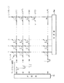
次に、図12を参照して図7ないし図11に示す光センサによって構成したマトリクススイッチについて説明する。図12では、光センサをフォトインタラプタを示すシンボルで表し、シンボル中の○印は発光ヘッド、これに対向する矩形部分を受光ヘッドとした。また、光センサは実際には図9に示すように直線状に並べられているが、マトリクススイッチとして表現するために、縦線と横線に掛け渡すように斜めに配置して示した。そのため、発光ヘッドは4つの方向の2つに対してビームを出射し、受光ヘッドは4つの方向の2つからビームを受けるように記載した。
【0061】
また、図12のマトリクスを構成する横線は、各光センサの発光ヘッドのリード線の一方が接続された入力回路を示し、縦線は受光ヘッドのリード線が接続された出力回路を示す。なお、発光ヘッドの他方のリード線は接地され、受光ヘッドの他方のリード線は光電流を供給する電源に接続されている。また、横線と縦線との交差部に鍵盤番号を付し、交差部から突出した斜めの線によって当該鍵盤番号に対応するシャッタを示した。また、特定の発光ヘッドまたは受光ヘッドを指す場合には、発光ヘッド3というように、その右隣に位置するシャッタに対応する鍵盤番号を付して説明する。
【0062】
図12に示すように、このキーセンサは、マトリクスの横線で示される出力回路a〜l(12個)にキースキャン信号を出力する送信部Trと、縦線で示される入力回路1〜8から押鍵を示す信号が入力される受信部Reとを備えている。キースキャン信号は、一定の極めて短い周期を持ったパルス電流であり、出力回路aから出力回路lまで間断なく順番に繰り返し出力される。
【0063】
各出力回路a〜lには、4個または3個の発光ヘッドのリード線が接続されている。すなわち、出力回路aには、2オクターブづつ離れた4つの発光ヘッド1,25,49,73のリード線が接続されている。また、出力回路bには、2オクターブづつ離れた4つの発光ヘッド3,27,51,75のリード線が接続されている。このように、発光ヘッドは2オクターブづつ飛んで出力回路a〜lに接続され、表1に示すものと同一の結線が構成されている。なお、入力回路aからiまでは、それぞれ4つの発光ヘッドのリード線が接続され、入力回路jからlまでは、それぞれ3つの発光ヘッドのリード線が接続されている。
【0064】
次に、各入力回路1〜8には、6個または4個の受光ヘッド20のリード線が接続されている。すなわち、入力回路1には、鍵盤番号で4づつ離れた6つの受光ヘッド2,6,10,14,18,22のリード線が接続されている。また、入力回路2には、鍵盤番号で4づつ離れた6つの受光ヘッド4,8,12,16,20,24のリード線が接続されている。このように、発光ヘッドは、鍵盤番号で4つ飛びで入力回路1〜8に接続され、表2に示すものと同一の結線が構成されている。
以上のように、このキーセンサのマトリクススイッチは、図4に示す第1の実施の形態のマトリクススイッチと同じ結線により構成されており、第1の実施の形態と同等に動作する。
【0065】
(4)変更例
▲1▼図10に示すケーシング80に、図1、図7および図8に示す発光ヘッドおよび受光ヘッドを収容して使用することができる。
▲2▼図11に示すLED95とフォトトランジスタ95をケーシング80に内蔵しないで用いることができる。
▲3▼図5に示すファイバサポートに、図7または図8に示す基体63または73を埋設することができる。
▲4▼シャッタ1aにスリットを形成してビームを2点検出式に構成することができる。すなわち、シャッタ1aの縁部がビームを遮った後に、スリットをビームが通過し、その後、スリットの縁部がビームを再び遮るように構成することができ、これにより、2回目にビームが遮られる時刻と1回目にビームが遮られる時刻から押鍵速度を算出することができる。
▲5▼ビームをシャッタの進行方向に沿って2列設けることができる。そのために、上記構成の光センサを2列設けることができ、発光ヘッドに光ファイバの端部や発光素子などの発光部を2つ設けるとともに、受光ヘッドに光ファイバの端部やフォトトランジスタなどの受光部を2つ設けることができる。さらに、この場合にも、シャッタにスリットを形成して4点検出式に構成することができる。
▲6▼プリズムは光を内面反射するように構成したが、その傾斜面に反射被膜をコーティングすることにより、入射角によらず光を全反射させるように構成することができる。
▲7▼上述した実施形態における発光手段(発光ヘッド)あるいは受光手段(受光ヘッド)のうちの何れか一方において、従来技術に示す構成を採用するようにしても、部品点数を削減できるという効果は得られる。
▲8▼上述した実施形態においては、12×8のマトリクススイッチを構成したが、行の数および列の数は如何なる値でもよく、1つの発光手段から出射された2つの光を異なる受光手段で受光するようにさえすれば、複数の発光手段と複数の受光手段とを複数の鍵にどのように割り付けるかは任意に変更可能である。
▲9▼本発明は、鍵の動作を検出するキーセンサのみならず、ハンマの動作を検出するハンマセンサにも適用することができる。たとえば、ハンマシャンクあるいはキャッチャシャンクにシャッタを取り付け、押鍵に応じて回動するシャッタがビームを遮るように構成することができる。加えて、楽器に限らず他分野にも適用可能である。
【0066】
【発明の効果】
以上説明したようにこの発明の情報出力装置においては、1つの発光手段とその両側に配置した受光手段によって2つの対象物を検出することができるので、光ファイバや電気配線の数を大幅に低減することができる(請求項1)。
また、請求項1に記載の構成に用いることにより、光ファイバや電気配線の数を大幅に低減した演奏情報出力装置を構成することができる(請求項2,5)、さらに、光を有効に使用することができる(請求項3)。
【図面の簡単な説明】
【図1】本発明の第1の実施の形態のキーセンサを示す下面図である。
【図2】図1のII−II線断面図である。
【図3】第1の実施の形態における光ファイバの接続状態を示す図である。
【図4】本発明のキーマトリクスを説明するための図である。
【図5】本発明の第2の実施の形態のキーセンサを示す平面図である。
【図6】図5のVI−VI線断面図である。
【図7】本発明の第3の実施の形態である光センサを示す平面図である。
【図8】図7に示す発光ヘッドの変更例を示す平面図である。
【図9】図7に示す光センサをケーシングに収容して配列した状態を示す正面図である。
【図10】(A)はケーシングの内部を示す断面図、(B)はその側面図、(C)はケーシングの他の例を示す側面図である。
【図11】図10(A)に示す光センサの変更例を示す断面図である。
【図12】図7ないし図11のずれかに示す光センサでマトリクススイッチを構成した結線状態を示す図である。
【図13】従来の機械式スイッチを示す側面図である。
【図14】従来の機械式スイッチの他の例を示す側面図である。
【図15】従来のフォトインタラプタを用いた光センサを示す正面図である。
【図16】従来のファイバセンサを用いた光センサを示す平面図である。
【図17】従来の機械式スイッチでマトリクススイッチを構成した場合の結線状態を示す図である。
【図18】従来のフォトインタラプタでマトリクススイッチを構成した場合の結線状態を示す図である。
【図19】従来のファイバセンサでマトリクススイッチを構成した場合の結線状態を示す図である。
【符号の説明】
1…鍵、1a…シャッタ(対象物)、20…センサヘッド、
20a…発光ヘッド(発光手段)、20b…受光ヘッド(受光手段)、
25…光ファイバ、21a…傾斜面(反射部)、64…発光素子、
74…受光素子、90…LED(発光素子)、
95…フォトトランジスタ(受光素子)。[0001]
TECHNICAL FIELD OF THE INVENTION
The present invention detects a key or a hammer operation in a keyboard instrument and outputs a signal. signal The present invention relates to an output device and an optical sensor used for the output device.
[0002]
[Prior art]
2. Description of the Related Art Conventionally, keyboard instruments such as an automatic performance piano and a silence performance piano have been provided, and such a keyboard instrument includes a performance information output device that detects an operation of a key or a hammer during performance and outputs a signal. . The signal output from the performance information output device is recorded on a recording means such as a floppy disk or the like as performance data for driving a key during a playback performance in an automatic performance piano. Is used electronically.
[0003]
Conventionally, as a performance information output device as described above, as shown in FIGS. 13 and 14, a mechanical switch 3 (or 4) is provided on an upper surface of a
Further, the
[0004]
Further, a key sensor using an optical sensor instead of the mechanical switch as described above is also supplied. FIG. 15 is an example in which a key sensor is configured using the
[0005]
FIG. 16 is a diagram showing a key sensor using a fiber sensor developed by the present applicant. This fiber sensor includes
[0006]
With this configuration, the beam emitted from the end face of the
[0007]
The above is the configuration of the key sensor that detects the operation of the key in the conventional performance information output device. The performance information output device determines the key related to the key depression by determining which mechanical switch or optical sensor has received the signal. Is detected.
By the way, since a piano has 88 keys, if the outputs of all the optical sensors and the like are individually input from the reception ports provided for each key sensor, 88 reception ports are required, and the device becomes difficult. It becomes extremely complicated. Therefore, conventionally, a key switch is performed by configuring a matrix switch by dividing an input system and an output system to an optical sensor or the like.
[0008]
FIG. 17 is a diagram illustrating an example in which a matrix switch is configured by the
[0009]
Here,
[0010]
The key sensor includes a transmission unit Tr that outputs a key scan signal to an input circuit indicated by a horizontal line of the matrix switch, and a reception unit Re that receives a signal from an output circuit indicated by a vertical line. The key scan signal is a pulse current having a certain extremely short cycle, and is repeatedly output in order from the input circuit belonging to the note number a to the input circuit belonging to the note number l without duplication.
Now, assuming that the key of the
As described above, the performance information output device can detect the key pressed by the note number indicated by the timing at which the signal is input to the reception unit Re and the octave indicated by the output terminal to which the signal is input. In addition, there is a difference between the timing at which the switch is turned on and the timing at which a signal is input to the receiving unit Re. However, since the difference is extremely short, no problem occurs.
[0011]
Next, FIG. 18 shows an example in which a matrix switch is configured by the photo interrupter shown in FIG. The matrix switch shown in this figure is obtained by replacing the switch shown in FIG. 17 with the
FIG. 19 shows an example in which a matrix switch is constituted by the
[0012]
As shown in FIG. 19, the optical fibers on the light receiving side of each fiber sensor are bundled for each octave, and their end faces face the phototransistor PTr of the receiving unit. Since there are 12 note numbers in each octave, the end faces of 12 optical fibers face each phototransistor RTr. However, since the keyboard number is up to # 88, there are four optical fibers facing the phototransistor RTr belonging to eight octaves.
The optical fibers on the light emitting side of each fiber sensor are bundled for each note number, and their end faces are opposed to the LED of the transmitting unit. Since the keyboard numbers range from one octave to eight octaves, the end faces of eight optical fibers face each LED. However, since the keyboard number is up to # 88, there are seven optical fibers facing the LEDs belonging to the note numbers e to l, respectively.
[0013]
In this key sensor, a key scan signal is output from the LED of the transmission unit. The key scan signal is a light pulse having a certain extremely short period, and is repeatedly output in order from the LED belonging to the note number a to the LED belonging to the note number l without overlapping. When a light pulse is emitted from one LED, the light pulse is transmitted to each of the fiber sensors through the eight optical fibers on the emitting side. Then, the light pulse beam transmitted to the adjacent fiber sensor is transmitted through the optical fiber on the light receiving side and received by each phototransistor PTr belonging to 1 octave to 8 octaves, and each phototransistor PTr receives the light of the received light. Generates a current corresponding to the quantity.
[0014]
Now, assuming that the key of the
[0015]
As described above, the key sensor can detect the key pressed by the note number indicated by the timing when the output current of the specific phototransistor PTr falls below the predetermined threshold value and the octave to which the phototransistor belongs. Further, by arranging the key sensors as described above in two rows along the traveling direction of the shutter, the key pressing speed is calculated from the time when the shutter interrupts the first beam and the time when the next beam is interrupted. Things are also provided.
[0016]
[Problems to be solved by the invention]
However, the key sensor that performs the key scan using the above fiber sensor also has the following improvements.
{Circle around (1)} Since 88 fiber sensors are required, as many as 88 optical fibers are required on the issuing side and the light receiving side, respectively. Particularly, in a configuration in which key sensors are arranged in two rows, the number of optical fibers is doubled. For this reason, a large amount of labor is required for assembling the fiber sensor and the like, and the maintenance and inspection work is also complicated. Of course, a performance information output device that performs a key scan using a mechanical switch also has the same problem that the wiring work and the maintenance and inspection work are complicated.
{Circle over (2)} Since the prism of the fiber sensor is configured to internally reflect light, it reflects only light incident at an angle within the critical angle among incident light. In the fiber sensor having the above configuration, the light emitted from the optical fiber reaches the prism while expanding, so that a part of the light enters the prism at an incident angle exceeding the critical angle. Therefore, there is a disadvantage that efficiency is poor because only a part of the light is used.
[0017]
Therefore, the present invention has been made in view of the above circumstances, and can significantly reduce the number of optical fibers and electrical wiring. signal It is intended to provide an output device. Another object of the present invention is to provide an optical sensor that can effectively use light.
[Means for Solving the Problems]
[0018]
[0019]
The optical sensor according to
[0020]
The optical sensor according to
[0021]
According to a fourth aspect of the present invention, in the optical sensor according to the second or third aspect, the pair of reflections is provided on the sensor head. surface Light-emitting element that emits light toward the boundary of One pair Reflection surface And a light receiving element for receiving the light internally reflected by the light emitting element is provided.
[0022]
According to a fifth aspect of the present invention, in the optical sensor according to the second or third aspect, the pair of reflections is provided on the sensor head. surface Emit light toward the boundary of One pair Reflection surface And an end portion of an optical fiber for receiving the light reflected internally.
[0023]
The light sensor according to
[0024]
[0025]
Further, in the optical sensor according to the second aspect, the light emitted from the light emitting portion is substantially V-shaped and is internally reflected so as to be distributed to both sides by the adjacent reflecting portion, so that one light emitting portion Light can be emitted in two directions. Further, light incident from two light emitting units can be received by one light receiving unit. Therefore, by using this optical sensor in the configuration of the first aspect, it is possible to configure a performance information output device in which the number of optical fibers and electrical wirings is significantly reduced.
In the optical sensor according to the third aspect, since the optical axis of the light emitted from the light emitting section substantially coincides with the bisector of the reflecting sections, the angle of incidence of the light incident on each reflecting section. Is small. Therefore, by appropriately setting the angle formed between the reflection portions, the light incident on the reflection portion can be totally reflected by setting the incident angle of the light to the critical angle or less, and thus the light can be used effectively.
[0026]
Furthermore, in the optical sensor according to the sixth aspect, the light emitted from the pair of light emitting elements can be directed to both sides, and the light emitted from the light emitting elements on both sides can be received by the pair of light receiving elements. Therefore, by using the configuration of the first aspect, it is possible to configure a performance information output device in which the number of optical fibers and electrical wirings is significantly reduced.
[0027]
BEST MODE FOR CARRYING OUT THE INVENTION
(1) First embodiment
A. Key sensor configuration
Hereinafter, a first embodiment of the present invention will be described with reference to FIGS.
FIG. 1 is a bottom view showing a key sensor (performance information output device) according to the embodiment. This key sensor is designed to be attached to the lower side of a keyboard of a keyboard instrument such as an automatic performance piano or a silence performance piano. In FIG. 1,
[0028]
A
[0029]
The end surface of the free end of each
[0030]
As described above, in the key sensor according to the present embodiment, the light emitting heads 20a and the light receiving heads 20b are alternately arranged, and the pressing of the
[0031]
B. Configuration of matrix switch
As shown in FIG. 3, this key sensor is composed of a transmitting section having twelve LEDs labeled a to l in the figure and a receiving section having eight phototransistors PTr labeled 1 to 8. Section. In the following description, when any one of the LED and the phototransistor PTr is specified and indicated, a description will be given with a subscript indicating a group such as “LEDa” or “PTr1”. In addition, when any one of the light emitting head 20a and the
[0032]
Optical fibers of four or three light emitting heads 20a are bundled with each LED, and their end faces are opposed to each other. That is, the optical fibers of the four light emitting heads 20a1, 20a25, 20a49, and 20a73 separated by two octaves are connected to the LEDa. The optical fibers of four light emitting heads 20a3, 20a27, 20a51, and 20a75 separated by two octaves are connected to LEDb. Table 1 summarizes the connection state of the light emitting head 20a shown in FIG. In FIG. 4, the circles indicate the light emitting heads 20a and the black circles indicate the light receiving heads 20b, and the numbers between the light emitting heads 20a and the light receiving heads 20b indicate the keyboard numbers of the keys arranged there. Since the number of keys is 88, the number of light emitting heads is 45 and the number of light receiving heads is 44. Although the number of the light emitting head 20a located at the rightmost end is 89, the keyboard number # 89 does not exist.
[0033]
[Table 1]
As can be seen from Table 1, the LED is connected to the optical fiber of the light emitting head 20a every two octaves, and the next LED is connected to the optical fiber of the light emitting head 20a which is shifted by two from the former. . Further, from LEDa to LEDi, the optical fibers of four light emitting heads 20a are respectively connected, and from LEDj to LED1, the optical fibers of three light emitting heads 20a are connected since the light emitting head 20a is # 89. Have been. Therefore, as described above, the light emitting head 20a has a total of 45 optical fibers.
[0035]
Next, the connection of the optical fiber of the
[0036]
[Table 2]
As can be seen from Table 2, the phototransistor PTr is connected to the optical fiber of the
[0038]
C. Operation of the embodiment
(1) Function of sensor head
First, a key scan signal is output from the LED of the transmission unit. The key scan signal is a light pulse having a certain extremely short period, and is repeatedly output without interruption from LEDa to LEDl. The light pulse is transmitted through the
[0039]
Next, the beam emitted from the
[0040]
Here, when the
[0041]
(2) Key scan operation
Next, a key scanning operation of the key sensor will be described with reference to FIG. In the following description, when referring to a key having a specific keyboard number, the description will be made with a keyboard number such as
The LEDs a to l of the transmitter repeat the output of the optical pulse signal without interruption in an extremely short cycle in that order. When one of the LEDs a to l outputs a light pulse signal, the light is transmitted to the light emitting head 20a shown in Table 1, and a light beam is emitted from the light emitting head 20a to the light receiving heads 20b, 20b on both sides thereof.
If the
[0042]
When the
[0043]
In the key sensor having the above configuration, by performing the key scan as described above, all keys can be separately detected even if only one
Further, since the
[0044]
(2) Second embodiment
A. Configuration of Second Embodiment
Next, a second embodiment of the present invention will be described with reference to FIGS. The second embodiment differs from the first embodiment only in that an optical fiber is attached to a fiber support provided at a distance from the sensor head. Therefore, in the following description, the same reference numerals are given to the same components as those in the above-described embodiment, and the description is omitted.
In the figure,
[0045]
Next, on the
[0046]
The light-receiving
[0047]
B. Operation of the second embodiment
The light emitted from the
[0048]
The light incident on the light emitting head 30a is refracted by the
[0049]
In the optical sensor having the above configuration, when the key is pressed and the shutter 1a enters the optical path of the beam, the shutter 1a interferes with the intermittently generated beam as described above. As a result, the amount of light received by the phototransistor to which the
[0050]
Thus, when the shutter 1a is traversing the optical path of the beam, the amount of light received by the phototransistor continuously decreases, and the output current of the phototransistor decreases each time. Therefore, with this key sensor, it is possible to determine the temporal change of the position of the shutter 1a, that is, the
In particular, in this embodiment, the cross-sectional shape of the light is made into a vertically long elliptical shape by the
[0051]
(3) Third embodiment
A. Optical sensor configuration
Next, a third embodiment of the present invention will be described with reference to FIG. The third embodiment is characterized in that the optical sensor is configured to be equivalent to a photo interrupter. As shown in FIG. 7, the
[0052]
Next, the
[0053]
The
[0054]
The beam emitted from the
[0055]
Such an optical sensor has the same operation and effect as the optical sensor according to the above-described embodiment. In particular, in this optical sensor, since the
[0056]
Next, FIG. 8 shows a modified example of the
[0057]
As shown in FIG. 10C, a
[0058]
As shown in FIG. 10A, the
Further, as shown in FIG. 11, an
[0059]
Similarly to the
[0060]
B. Configuration of matrix switch
Next, a matrix switch constituted by the optical sensors shown in FIGS. 7 to 11 will be described with reference to FIG. In FIG. 12, the optical sensor is represented by a symbol indicating a photointerrupter, and a circle in the symbol represents a light emitting head, and a rectangular portion opposed to the light receiving head represents a light receiving head. Although the optical sensors are actually arranged in a straight line as shown in FIG. 9, they are shown diagonally so as to cross over a vertical line and a horizontal line in order to represent a matrix switch. Therefore, it has been described that the light emitting head emits beams in two directions in four directions, and the light receiving head receives beams in two directions in four directions.
[0061]
In addition, the horizontal lines forming the matrix in FIG. 12 indicate input circuits to which one of the leads of the light emitting head of each optical sensor is connected, and the vertical lines indicate the output circuits to which the leads of the light receiving head are connected. The other lead of the light emitting head is grounded, and the other lead of the light receiving head is connected to a power supply for supplying a photocurrent. In addition, a keyboard number is assigned to an intersection between the horizontal line and the vertical line, and a shutter corresponding to the keyboard number is indicated by an oblique line protruding from the intersection. When a specific light emitting head or light receiving head is indicated, a key number corresponding to a shutter located on the right side of the
[0062]
As shown in FIG. 12, this key sensor receives a signal from a transmitting unit Tr that outputs a key scan signal to output circuits a to l (12) indicated by horizontal lines of a matrix and
[0063]
To each of the output circuits a to l, lead wires of four or three light emitting heads are connected. That is, the output circuit a is connected to the lead wires of the four
[0064]
Next, to each of the
As described above, the matrix switch of the key sensor has the same connection as the matrix switch of the first embodiment shown in FIG. 4, and operates in the same manner as the first embodiment.
[0065]
(4) Modification example
{Circle around (1)} The light emitting head and the light receiving head shown in FIGS. 1, 7 and 8 can be accommodated and used in a
(2) The
(3) The
{Circle around (4)} A slit can be formed in the shutter 1a to form a two-point detection type beam. That is, the beam may pass through the slit after the edge of the shutter 1a blocks the beam, and then the edge of the slit may block the beam again, thereby blocking the beam a second time. The key pressing speed can be calculated from the time and the time when the beam is interrupted for the first time.
{Circle around (5)} Two beams can be provided along the traveling direction of the shutter. For this purpose, two rows of optical sensors having the above configuration can be provided. The light emitting head is provided with two light emitting portions such as an end of an optical fiber and a light emitting element, and the light receiving head is provided with an end of an optical fiber and a phototransistor. Two light receiving units can be provided. Further, also in this case, a slit can be formed in the shutter so that the shutter can be configured as a four-point detection type.
{Circle around (6)} Although the prism is configured to internally reflect light, the prism may be configured to totally reflect light regardless of the incident angle by coating the inclined surface with a reflective film.
{Circle around (7)} Either one of the light emitting means (light emitting head) and the light receiving means (light receiving head) in the above-described embodiment adopts the configuration shown in the prior art, but the effect of reducing the number of parts is still small. can get.
(8) In the above-described embodiment, a 12 × 8 matrix switch is configured. However, the number of rows and the number of columns may be any value, and two lights emitted from one light emitting unit may be received by different light receiving units. As long as light is received, how the plurality of light emitting means and the plurality of light receiving means are assigned to the plurality of keys can be arbitrarily changed.
(9) The present invention can be applied not only to a key sensor for detecting a key operation but also to a hammer sensor for detecting a hammer operation. For example, a shutter can be attached to a hammer shank or a catcher shank, so that a shutter that rotates in response to a key depression can block the beam. In addition, it is applicable not only to musical instruments but also to other fields.
[0066]
【The invention's effect】
As described above, in the information output apparatus of the present invention, two objects can be detected by one light emitting means and the light receiving means arranged on both sides thereof, so that the number of optical fibers and electrical wiring is greatly reduced. (Claim 1).
Also, by using the configuration of the first aspect, it is possible to configure a performance information output device in which the number of optical fibers and electrical wirings is significantly reduced (
[Brief description of the drawings]
FIG. 1 is a bottom view showing a key sensor according to a first embodiment of the present invention.
FIG. 2 is a sectional view taken along line II-II of FIG.
FIG. 3 is a diagram illustrating a connection state of optical fibers according to the first embodiment.
FIG. 4 is a diagram for explaining a key matrix of the present invention.
FIG. 5 is a plan view showing a key sensor according to a second embodiment of the present invention.
FIG. 6 is a sectional view taken along line VI-VI of FIG. 5;
FIG. 7 is a plan view showing an optical sensor according to a third embodiment of the present invention.
FIG. 8 is a plan view showing a modification of the light emitting head shown in FIG.
9 is a front view showing a state where the optical sensors shown in FIG. 7 are housed in a casing and arranged.
10A is a sectional view showing the inside of a casing, FIG. 10B is a side view thereof, and FIG. 10C is a side view showing another example of the casing.
FIG. 11 is a cross-sectional view showing a modification of the optical sensor shown in FIG.
FIG. 12 is a diagram showing a connection state in which a matrix switch is formed by the optical sensors shown in FIGS. 7 to 11;
FIG. 13 is a side view showing a conventional mechanical switch.
FIG. 14 is a side view showing another example of the conventional mechanical switch.
FIG. 15 is a front view showing a photosensor using a conventional photointerrupter.
FIG. 16 is a plan view showing an optical sensor using a conventional fiber sensor.
FIG. 17 is a diagram illustrating a connection state when a matrix switch is configured by a conventional mechanical switch.
FIG. 18 is a diagram illustrating a connection state when a matrix switch is configured by a conventional photo interrupter.
FIG. 19 is a diagram illustrating a connection state when a matrix switch is configured by a conventional fiber sensor.
[Explanation of symbols]
DESCRIPTION OF
20a: light emitting head (light emitting means), 20b: light receiving head (light receiving means),
25: optical fiber, 21a: inclined surface (reflection portion), 64: light emitting element,
74: light receiving element, 90: LED (light emitting element),
95 ... Phototransistor (light receiving element).
Claims (6)
上記発光手段に光を発生させるための信号を出力する送信部と、上記受光手段が受光した光を信号として受信する受信部とを設け、
上記発光手段は、1つの発光部から2つの移動体に対して光を出射し、
上記受光手段は、2つの発光手段から出射された光を1つの受光部で受光し、
上記発光手段と上記受光手段とを複数交互に配設するとともに、1つの発光手段から出射された2つの光を異なる受光手段で受光するように配設し、
上記送信部は、複数の発光手段について各々異なるタイミングで発光させるようにしたことを特徴とする信号出力装置。A light path for causing a beam emitted from the light emitting means to be incident on the light receiving means ; detecting whether or not a moving body blocks an optical path between the light emitting means and the light receiving means; and a signal corresponding to the detection. In a signal output device that outputs
A transmitting unit that outputs a signal for generating light to the light emitting unit, and a receiving unit that receives the light received by the light receiving unit as a signal,
The light emitting means emits light from one light emitting unit to two moving bodies,
The light receiving means receives light emitted from the two light emitting means by one light receiving unit,
A plurality of the light emitting means and the light receiving means are arranged alternately, and two light emitted from one light emitting means are arranged to be received by different light receiving means,
The signal output device, wherein the transmitting unit causes the plurality of light emitting units to emit light at different timings.
上記センサヘッドは、
光を透過する部材によって略矩形状に形成されており、
両隣に設けられたセンサヘッドと対向する2つの側面と、
上記発光部または上記受光部と対向する1の面と、
上記1の面と対向する面をV字状に切り欠いて形成された1対の反射面とを有し、
上記発光部から出射され、上記1の面の側から入射された光を上記1対の反射面により内面反射させて上記2つの側面から両隣のセンサヘッドに向けて出射する一方、両隣のセンサヘッドの側面から出射され、上記2つの側面から各々入射された光を上記1対の反射面により内面反射させて上記1の面の側に出射し、上記受光部に入射させる
ことを特徴とする光センサ。 A light emitting unit, a light receiving portion provided at a position spaced a light emitting portion, the light emitted from the light emitting portion is arranged on an optical path to be incident on the light receiving portion, and a plurality of sensor heads that transmit light An optical sensor for detecting whether or not a moving body has blocked an optical path between the sensor heads,
The sensor head is
It is formed in a substantially rectangular shape by a member that transmits light,
Two side faces facing the sensor head provided on both sides,
A surface facing the light emitting unit or the light receiving unit;
A pair of reflecting surfaces formed by cutting out a surface facing the first surface in a V-shape,
The light emitted from the light emitting portion and incident from the side of the first surface is internally reflected by the pair of reflecting surfaces and emitted from the two side surfaces toward the sensor heads on both sides, while the sensor heads on both sides are provided. The light emitted from the two side surfaces and incident from the two side surfaces is internally reflected by the pair of reflecting surfaces, emitted to the one surface side, and made incident on the light receiving unit.
Light sensor, wherein a call.
Priority Applications (6)
| Application Number | Priority Date | Filing Date | Title |
|---|---|---|---|
| JP31318495A JP3552374B2 (en) | 1995-11-30 | 1995-11-30 | Signal output device and optical sensor |
| TW085114171A TW321761B (en) | 1995-11-30 | 1996-11-19 | |
| US08/754,253 US5909028A (en) | 1995-11-30 | 1996-11-20 | Position transducer and positional information processing system using the same |
| CNB961213655A CN1184612C (en) | 1995-11-30 | 1996-11-30 | Position sensor and information process system using it |
| KR1019960060322A KR100200562B1 (en) | 1995-11-30 | 1996-11-30 | Position transducer and positional information processing system using the same |
| DE19649928A DE19649928C2 (en) | 1995-11-30 | 1996-12-02 | position transducer |
Applications Claiming Priority (1)
| Application Number | Priority Date | Filing Date | Title |
|---|---|---|---|
| JP31318495A JP3552374B2 (en) | 1995-11-30 | 1995-11-30 | Signal output device and optical sensor |
Publications (2)
| Publication Number | Publication Date |
|---|---|
| JPH09152871A JPH09152871A (en) | 1997-06-10 |
| JP3552374B2 true JP3552374B2 (en) | 2004-08-11 |
Family
ID=18038118
Family Applications (1)
| Application Number | Title | Priority Date | Filing Date |
|---|---|---|---|
| JP31318495A Expired - Fee Related JP3552374B2 (en) | 1995-11-30 | 1995-11-30 | Signal output device and optical sensor |
Country Status (6)
| Country | Link |
|---|---|
| US (1) | US5909028A (en) |
| JP (1) | JP3552374B2 (en) |
| KR (1) | KR100200562B1 (en) |
| CN (1) | CN1184612C (en) |
| DE (1) | DE19649928C2 (en) |
| TW (1) | TW321761B (en) |
Families Citing this family (29)
| Publication number | Priority date | Publication date | Assignee | Title |
|---|---|---|---|---|
| AU6419798A (en) * | 1997-03-19 | 1998-10-12 | Omron Corporation | Transmitting photoelectric sensor array |
| DE19835884A1 (en) * | 1998-08-07 | 2000-02-10 | Sick Ag | Light curtain |
| JP4081908B2 (en) * | 1998-09-18 | 2008-04-30 | ヤマハ株式会社 | Operational amplifier offset voltage compensator |
| JP3997657B2 (en) * | 1999-07-21 | 2007-10-24 | ヤマハ株式会社 | Automatic playing device for keyboard instruments |
| JP2001083965A (en) * | 1999-09-16 | 2001-03-30 | Namco Ltd | Plucked string type electronic instrument |
| KR100798048B1 (en) * | 2000-03-08 | 2008-01-24 | 기븐 이미징 리미티드 | A capsule for in vivo imaging |
| JP4595193B2 (en) * | 2000-11-17 | 2010-12-08 | ヤマハ株式会社 | Hammer detection device |
| JP4221896B2 (en) * | 2000-11-30 | 2009-02-12 | ヤマハ株式会社 | Optical fiber sensor |
| JP4374803B2 (en) * | 2001-06-26 | 2009-12-02 | ヤマハ株式会社 | Optical sensor |
| JP3820936B2 (en) * | 2001-07-31 | 2006-09-13 | ヤマハ株式会社 | Key sensor, key sensor detection board and keyboard instrument |
| JP3922085B2 (en) | 2002-04-25 | 2007-05-30 | ヤマハ株式会社 | Optical fiber bundle holding structure |
| JP3849570B2 (en) * | 2002-04-25 | 2006-11-22 | ヤマハ株式会社 | Motion detection parts |
| JP3979168B2 (en) * | 2002-04-26 | 2007-09-19 | ヤマハ株式会社 | Light emitting part structure in a key depression detection device for a keyboard instrument |
| US7417624B2 (en) * | 2003-02-14 | 2008-08-26 | Duff Michael J | Zero-force key activation keyboard with dynamic individual key illumination |
| JP4284650B2 (en) | 2003-09-18 | 2009-06-24 | ヤマハ株式会社 | Optical detector |
| JP4360172B2 (en) * | 2003-10-09 | 2009-11-11 | ヤマハ株式会社 | Optical fiber holding member |
| JP4129798B2 (en) * | 2004-01-06 | 2008-08-06 | ヤマハ株式会社 | Optical detector |
| JP4552227B2 (en) | 2005-01-24 | 2010-09-29 | ヤマハ株式会社 | Position detection device |
| JP5209287B2 (en) * | 2007-12-13 | 2013-06-12 | ローランド株式会社 | Electronic musical instrument operation position detection device |
| US7825312B2 (en) * | 2008-02-27 | 2010-11-02 | Steinway Musical Instruments, Inc. | Pianos playable in acoustic and silent modes |
| US8148620B2 (en) * | 2009-04-24 | 2012-04-03 | Steinway Musical Instruments, Inc. | Hammer stoppers and use thereof in pianos playable in acoustic and silent modes |
| US8541673B2 (en) | 2009-04-24 | 2013-09-24 | Steinway Musical Instruments, Inc. | Hammer stoppers for pianos having acoustic and silent modes |
| WO2014009466A2 (en) * | 2012-07-11 | 2014-01-16 | Tyco Electronics Raychem Bvba | Presence detection using leds in rfid physical layer management system |
| US20150122112A1 (en) * | 2013-11-03 | 2015-05-07 | Miselu Inc. | Sensing key press activation |
| JP6729939B2 (en) * | 2014-08-23 | 2020-07-29 | ムン キ イ, | Line division optical module and electronic keyboard using the same |
| JP6524940B2 (en) * | 2016-03-01 | 2019-06-05 | ヤマハ株式会社 | Detection device and program |
| JP7073620B2 (en) * | 2016-10-31 | 2022-05-24 | ヤマハ株式会社 | Actuator drive control device |
| US10482859B1 (en) * | 2018-09-13 | 2019-11-19 | Jammy Instruments Ltd. | Optical sensor and electric stringed musical instrument with digital interface (MIDI) equipped with optical sensor |
| CN115206272A (en) * | 2022-02-22 | 2022-10-18 | 蒋恩良 | Electronic keyboard musical instrument |
Family Cites Families (13)
| Publication number | Priority date | Publication date | Assignee | Title |
|---|---|---|---|---|
| DE2526001A1 (en) * | 1975-06-11 | 1976-12-23 | Precitec Gmbh | Optical object tracking system - uses set of corresponding lamps and photocells in two planes between which object moves |
| US4114144A (en) * | 1976-08-12 | 1978-09-12 | Imed Corporation | Automatic air-in-line fluid detector |
| DD131295B1 (en) * | 1976-12-22 | 1980-08-06 | Alfred Trappe | MULTI-CHANNEL, REDUNDANT LIGHTING DEVICE FOR FILL LEVEL OR POSITION CHECK |
| US4351221A (en) * | 1979-06-15 | 1982-09-28 | Teledyne Industries, Incorporated | Player piano recording system |
| FR2596222B1 (en) * | 1986-03-19 | 1992-02-07 | Souloumiac Alain | IMPROVEMENT OF OPTICAL KEYBOARDS |
| US4836636A (en) * | 1986-11-13 | 1989-06-06 | The Furukawa Electric Co., Ltd. | Optical switch and optical keyboard utilizing the same |
| US4935621A (en) * | 1987-10-30 | 1990-06-19 | Pikulski Joseph L | Optical switch with collimating lenses, antifreeze and/or index matching fluid for control of electrical equipment |
| DE68929035T2 (en) * | 1988-01-29 | 2000-03-23 | Yamaha Corp | Automatic piano with determination of the velocity |
| US5001339A (en) * | 1989-03-27 | 1991-03-19 | Gulbransen, Inc. | Opto-electronic sensing method and device for an acoustic piano |
| DE9100575U1 (en) * | 1991-01-22 | 1992-02-20 | Siemens Ag, 8000 Muenchen, De | |
| US5374775A (en) * | 1992-06-09 | 1994-12-20 | Yamaha Corporation | Keyboard instrument for selectively producing mechanical sounds and synthetic sounds without any mechanical vibrations on music wires |
| US5384459A (en) * | 1993-06-01 | 1995-01-24 | Motorola, Inc. | Illuminated switch and keypad assembly having a light gradient and a light conductive elastomeric assembly |
| JP3610648B2 (en) * | 1995-11-30 | 2005-01-19 | ヤマハ株式会社 | Optical sensor |
-
1995
- 1995-11-30 JP JP31318495A patent/JP3552374B2/en not_active Expired - Fee Related
-
1996
- 1996-11-19 TW TW085114171A patent/TW321761B/zh not_active IP Right Cessation
- 1996-11-20 US US08/754,253 patent/US5909028A/en not_active Expired - Lifetime
- 1996-11-30 KR KR1019960060322A patent/KR100200562B1/en not_active IP Right Cessation
- 1996-11-30 CN CNB961213655A patent/CN1184612C/en not_active Expired - Lifetime
- 1996-12-02 DE DE19649928A patent/DE19649928C2/en not_active Expired - Lifetime
Also Published As
| Publication number | Publication date |
|---|---|
| DE19649928C2 (en) | 2003-04-30 |
| TW321761B (en) | 1997-12-01 |
| JPH09152871A (en) | 1997-06-10 |
| KR970029318A (en) | 1997-06-26 |
| US5909028A (en) | 1999-06-01 |
| DE19649928A1 (en) | 1997-06-05 |
| CN1184612C (en) | 2005-01-12 |
| KR100200562B1 (en) | 1999-06-15 |
| CN1159636A (en) | 1997-09-17 |
Similar Documents
| Publication | Publication Date | Title |
|---|---|---|
| JP3552374B2 (en) | Signal output device and optical sensor | |
| US4736662A (en) | Optical sensor for sensing displacement speed or displacement of a moveable element in musical instrument | |
| KR100907592B1 (en) | Optical transducer systems, optical modulators, and instruments using them for monitoring moving parts | |
| NL7920157A (en) | PHOTO-OPTICAL KEYBOARD. | |
| US5804816A (en) | Position transducer having optical beam generator for covering wide detectable range | |
| US4583733A (en) | Baseball bat swing measuring device | |
| JP3555117B2 (en) | Key sensor | |
| US6815603B2 (en) | Unbreakable and economical optical sensor array and keyboard musical instrument using the same | |
| CN1194335C (en) | Optical fibre sensor installed easily and music instrument using it | |
| JP3922085B2 (en) | Optical fiber bundle holding structure | |
| CN1607574B (en) | Optical transducer having optical modulator in the vicinity of rotational axis of moving object and musical instrument using the same | |
| JP3849570B2 (en) | Motion detection parts | |
| EP1587059A1 (en) | Keyboard musical instrument having sensor unit exactly located by means of plural locators | |
| JPS60231278A (en) | Optical reader | |
| JP3496374B2 (en) | Optical fiber sensor connector | |
| JPH09185374A (en) | Information output device | |
| EP0193556A1 (en) | Optical keyboard | |
| EP0089239B1 (en) | Fiber wrap keyboard and switch | |
| JPH0326470Y2 (en) | ||
| SU943775A1 (en) | Device for reading data from punch-cards | |
| JPS6220553B2 (en) | ||
| JPH0677025B2 (en) | Moving object recognition sensor | |
| JP3194673B2 (en) | Optical touch panel and input coordinate detection method using the same | |
| JPS59500637A (en) | optical keyboard | |
| JPH066399Y2 (en) | Performance information sensor for automatic piano |
Legal Events
| Date | Code | Title | Description |
|---|---|---|---|
| A131 | Notification of reasons for refusal |
Free format text: JAPANESE INTERMEDIATE CODE: A131 Effective date: 20040120 |
|
| A521 | Written amendment |
Free format text: JAPANESE INTERMEDIATE CODE: A523 Effective date: 20040318 |
|
| TRDD | Decision of grant or rejection written | ||
| A01 | Written decision to grant a patent or to grant a registration (utility model) |
Free format text: JAPANESE INTERMEDIATE CODE: A01 Effective date: 20040413 |
|
| A61 | First payment of annual fees (during grant procedure) |
Free format text: JAPANESE INTERMEDIATE CODE: A61 Effective date: 20040426 |
|
| R150 | Certificate of patent or registration of utility model |
Free format text: JAPANESE INTERMEDIATE CODE: R150 |
|
| S531 | Written request for registration of change of domicile |
Free format text: JAPANESE INTERMEDIATE CODE: R313532 |
|
| R350 | Written notification of registration of transfer |
Free format text: JAPANESE INTERMEDIATE CODE: R350 |
|
| FPAY | Renewal fee payment (event date is renewal date of database) |
Free format text: PAYMENT UNTIL: 20090514 Year of fee payment: 5 |
|
| FPAY | Renewal fee payment (event date is renewal date of database) |
Free format text: PAYMENT UNTIL: 20100514 Year of fee payment: 6 |
|
| FPAY | Renewal fee payment (event date is renewal date of database) |
Free format text: PAYMENT UNTIL: 20110514 Year of fee payment: 7 |
|
| FPAY | Renewal fee payment (event date is renewal date of database) |
Free format text: PAYMENT UNTIL: 20130514 Year of fee payment: 9 |
|
| FPAY | Renewal fee payment (event date is renewal date of database) |
Free format text: PAYMENT UNTIL: 20140514 Year of fee payment: 10 |
|
| LAPS | Cancellation because of no payment of annual fees |